object oriented system analysis and design chapter 5 : … microprocessor 8086 is a 16-bit cpu...
TRANSCRIPT

Microprocessors Chapter 4 : Microprocessor System
Compiled by: Er. Hari Aryal Email: [email protected] Reference: R. S. Gaonkar & D, V. Hall | 1
Chapter-4 Microprocessor System
A microcomputer consists of a set of components or modules of three basic types CPU memory
and I/O units which communicate with each other.
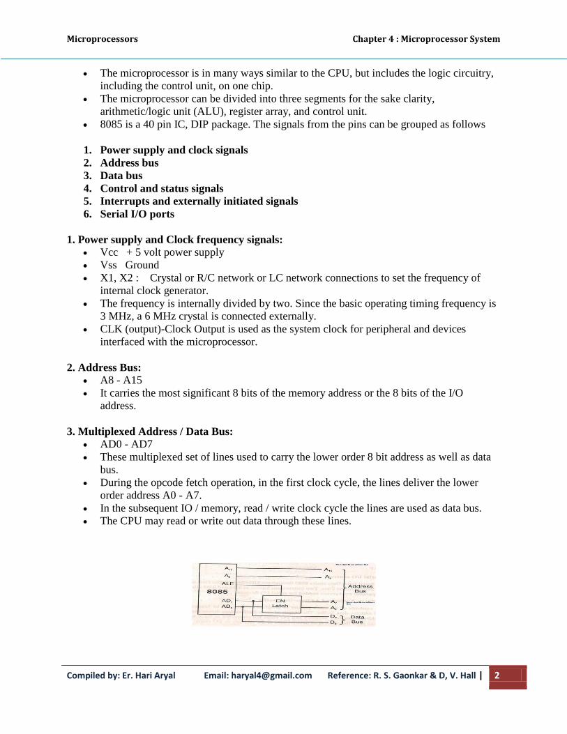
PIN Configuration of 8085
Fig (a) - Pin Diagram of 8085 & Fig(b) - logical schematic of Pin diagram
The microprocessor is a clock-driven semiconductor device consisting of electronic logic
circuits manufactured by using either a large-scale integration (LSI) or very-large-scale
integration (VLSI) technique.
The microprocessor is capable of performing various computing functions and making
decisions to change the sequence of program execution.
In large computers, a CPU implemented on one or more circuit boards performs these
computing functions.
Microprocessors Chapter 4 : Microprocessor System
Compiled by: Er. Hari Aryal Email: [email protected] Reference: R. S. Gaonkar & D, V. Hall | 2
The microprocessor is in many ways similar to the CPU, but includes the logic circuitry,
including the control unit, on one chip.
The microprocessor can be divided into three segments for the sake clarity,
arithmetic/logic unit (ALU), register array, and control unit.
8085 is a 40 pin IC, DIP package. The signals from the pins can be grouped as follows
1. Power supply and clock signals
2. Address bus
3. Data bus
4. Control and status signals
5. Interrupts and externally initiated signals
6. Serial I/O ports
1. Power supply and Clock frequency signals: Vcc + 5 volt power supply
Vss Ground
X1, X2 : Crystal or R/C network or LC network connections to set the frequency of
internal clock generator.
The frequency is internally divided by two. Since the basic operating timing frequency is
3 MHz, a 6 MHz crystal is connected externally.
CLK (output)-Clock Output is used as the system clock for peripheral and devices
interfaced with the microprocessor.
2. Address Bus:
A8 - A15
It carries the most significant 8 bits of the memory address or the 8 bits of the I/O
address.
3. Multiplexed Address / Data Bus:
AD0 - AD7
These multiplexed set of lines used to carry the lower order 8 bit address as well as data
bus.
During the opcode fetch operation, in the first clock cycle, the lines deliver the lower
order address A0 - A7.
In the subsequent IO / memory, read / write clock cycle the lines are used as data bus.
The CPU may read or write out data through these lines.
Microprocessors Chapter 4 : Microprocessor System
Compiled by: Er. Hari Aryal Email: [email protected] Reference: R. S. Gaonkar & D, V. Hall | 3
4. Control and Status signals:
These signals include two control signals (RD & WR) three status signals (IO/M, S1 and So) to
identify the nature of the operation and one special signal (ALE) ti indicate the beginning of the
operations.
ALE (output) - Address Latch Enable.
o This signal helps to capture the lower order address presented on the multiplexed
address / data bus. When it is the pulse, 8085 begins an operation. It generates AD0 - AD7 as the separate set of address lines A0 –A7.
RD (active low) - Read memory or IO device.
o This indicates that the selected memory location or I/O device is to be read and
that the data bus is ready for accepting data from the memory or I/O device.
WR (active low) - Write memory or IO device.
o This indicates that the data on the data bus is to be written into the selected
memory location or I/O device.
IO/M (output) - Select memory or an IO device.
o This status signal indicates that the read / write operation relates to whether the
memory or I/O device.
o It goes high to indicate an I/O operation.
o It goes low for memory operations.
5. Status Signals:
It is used to know the type of current operation of the microprocessor.
6. Interrupts and Externally initiated operations: They are the signals initiated by an external device to request the microprocessor to do a
particular task or work.
There are five hardware interrupts called,
On receipt of an interrupt, the microprocessor acknowledges the interrupt by the active
low INTA (Interrupt Acknowledge) signal.

Microprocessors Chapter 4 : Microprocessor System
Compiled by: Er. Hari Aryal Email: [email protected] Reference: R. S. Gaonkar & D, V. Hall | 4
Hold (Input)
This indicates peripheral controller requesting the bus.
HLDA (Output)
This indicates the acknowledgement for the Hold request.
READY (Input)
It is used to delay the microprocessor read and write cycles until a slow responding
peripheral is ready to send or accept data.
Memory and I/O devices will have slower response compared to microprocessors.
Before completing the present job such a slow peripheral may not be able to handle
further data or control signal from CPU.
The processor sets the READY signal after completing the present job to access the data.
The microprocessor enters into WAIT state while the READY pin is disabled.
Reset In (input, active low) This signal is used to reset the microprocessor.
The program counter inside the microprocessor is set to zero.
The buses are tri-stated.
Reset Out (Output) It indicates CPU is being reset.
Used to reset all the connected devices when the microprocessor is reset.
7. Single Bit Serial I/O ports: SID (input) - Serial input data line
SOD (output) - Serial output data line
These signals are used for serial communication.
Microprocessors Chapter 4 : Microprocessor System
Compiled by: Er. Hari Aryal Email: [email protected] Reference: R. S. Gaonkar & D, V. Hall | 5
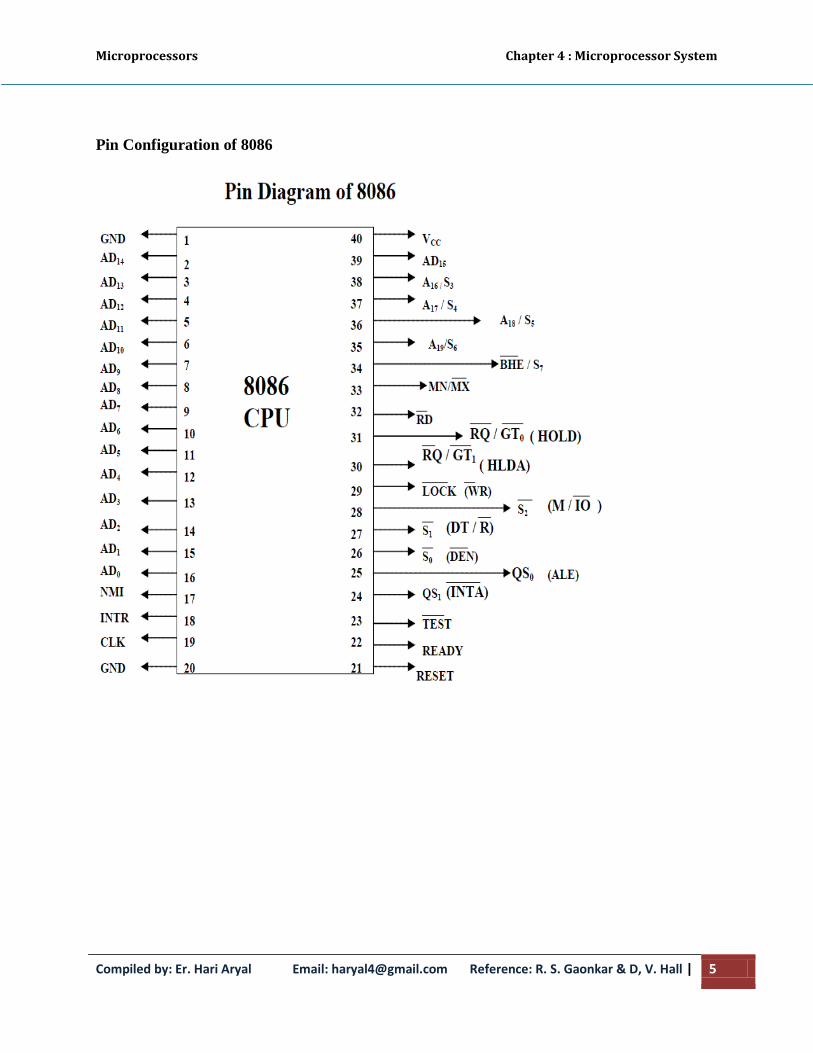
Pin Configuration of 8086
Microprocessors Chapter 4 : Microprocessor System
Compiled by: Er. Hari Aryal Email: [email protected] Reference: R. S. Gaonkar & D, V. Hall | 6
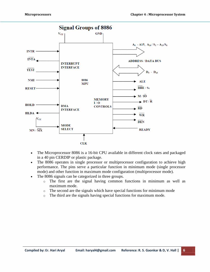
The Microprocessor 8086 is a 16-bit CPU available in different clock rates and packaged
in a 40 pin CERDIP or plastic package.
The 8086 operates in single processor or multiprocessor configuration to achieve high
performance. The pins serve a particular function in minimum mode (single processor
mode) and other function in maximum mode configuration (multiprocessor mode).
The 8086 signals can be categorized in three groups.
o The first are the signal having common functions in minimum as well as
maximum mode.
o The second are the signals which have special functions for minimum mode
o The third are the signals having special functions for maximum mode.
Microprocessors Chapter 4 : Microprocessor System
Compiled by: Er. Hari Aryal Email: [email protected] Reference: R. S. Gaonkar & D, V. Hall | 7
The following signal descriptions are common for both modes.
AD15-AD0 : These are the time multiplexed memory I/O address and data lines.
A19/S6,A18/S5,A17/S4,A16/S3 : These are the time multiplexed address and status
lines. The address bits are separated from the status bit using latches controlled by the
ALE signal.
BHE/S7 : The bus high enable is used to indicate the transfer of data over the higher
order ( D15-D8 ) data bus.
RD – Read : This signal on low indicates the peripheral that the processor is performing
memory or I/O read operation.
READY : This is the acknowledgement from the slow device or memory that they have
completed the data transfer.
INTR-Interrupt Request : This is to determine the availability of the request from
external devices. If any interrupt request is pending, the processor enters the interrupt
acknowledge cycle.
TEST : This input is examined by a ‘WAIT’ instruction. If the TEST pin goes low,
execution will continue, else the processor remains in an idle state.
CLK- Clock Input : The clock input provides the basic timing for processor operation
and bus control activity.
The following pin functions are for the minimum mode operation of 8086.
M/IO – Memory/IO : When it is low, it indicates the CPU is having an I/O operation,
and when it is high, it indicates that the CPU is having a memory operation.
INTA – Interrupt Acknowledge: This signal is used for interrupt acknowledge i.e.
when it goes low; the processor has accepted the interrupt.
ALE – Address Latch Enable: This output signal indicates the availability of the valid
address on the address/data lines.
DT/R – Data Transmit/Receive: This output is used to decide the direction of data flow
through the trans-receivers (bidirectional buffers). When the processor sends out data,
this signal is high and when the processor is receiving data, this signal is low.
DEN – Data Enable: This signal indicates the availability of valid data over the
address/data lines. It is used to enable the trans-receivers (bidirectional buffers) to
separate the data from the multiplexed address/data signal.
HOLD, HLDA- Acknowledge: When the HOLD line goes high, it indicates to the
processor that another master is requesting the bus access. The processor, after receiving
the HOLD request, issues the hold acknowledge signal on.
Microprocessors Chapter 4 : Microprocessor System
Compiled by: Er. Hari Aryal Email: [email protected] Reference: R. S. Gaonkar & D, V. Hall | 8
The following pin functions are applicable for maximum mode operation of 8086.
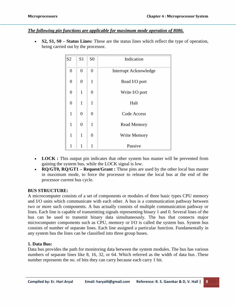
S2, S1, S0 – Status Lines: These are the status lines which reflect the type of operation,
being carried out by the processor.
S2 S1 S0 Indication
0
0
0
0
1
1
1
1
0
0
1
1
0
0
1
1
0
1
0
1
0
1
0
1
Interrupt Acknowledge
Read I/O port
Write I/O port
Halt
Code Access
Read Memory
Write Memory
Passive
LOCK : This output pin indicates that other system bus master will be prevented from
gaining the system bus, while the LOCK signal is low.
RQ/GT0, RQ/GT1 – Request/Grant : These pins are used by the other local bus master
in maximum mode, to force the processor to release the local bus at the end of the
processor current bus cycle.
BUS STRUCTURE:
A microcomputer consists of a set of components or modules of three basic types CPU memory
and I/O units which communicate with each other. A bus is a communication pathway between
two or more such components. A bus actually consists of multiple communication pathway or
lines. Each line is capable of transmitting signals representing binary 1 and 0. Several lines of the
bus can be used to transmit binary data simultaneously. The bus that connects major
microcomputer components such as CPU, memory or I/O is called the system bus. System bus
consists of number of separate lines. Each line assigned a particular function. Fundamentally in
any system bus the lines can be classified into three group buses.
1. Data Bus:
Data bus provides the path for monitoring data between the system modules. The bus has various
numbers of separate lines like 8, 16, 32, or 64. Which referred as the width of data bus .These
number represents the no. of bits they can carry because each carry 1 bit.
Microprocessors Chapter 4 : Microprocessor System
Compiled by: Er. Hari Aryal Email: [email protected] Reference: R. S. Gaonkar & D, V. Hall | 9
2. Address Bus:
Each Lines of address bus are used to designate the source or destination of the data on data bus.
For example, if the CPU requires reading a word (8, 16, 32) bits of data from memory, it puts the
address of desired word on address bus. The address bus is also used to address I/O ports. Bus
width determines the total memory the up can handle.
3. Control Bus:
The control bus is a group of lines used to control the access to control signals and the use of the
data and address bus. The control signals transmit both command and timing information
between the system modules. The timing signals indicate the validity of data and address
information, where as command signals specify operations to be performed. Some of the control
signals are:
Memory Write (MEMW): It causes data on the bus to be loaded in to the address location.
Memory Read (MEMR): It causes data from the addressed location to be placed on the data bus.
I/O Write (IOW): It causes the data on the bus to be output to the addressed I/O port.
I/O Read (IOR): It causes the data from the addressed I/O port to be placed on the bus.
Transfer Acknowledge: This signal indicates that data have been accepted from or placed on
the bus.
Bus Request: It is used to indicate that a module wants to gain control of the bus.
Bus Grant: It indicates that a requesting module has been granted for the control of bus.
Interrupt Request: It indicates that an interrupt has been pending.
Interrupt Acknowledge: it indicates that the pending interrupt has been recognized.
Bus Types
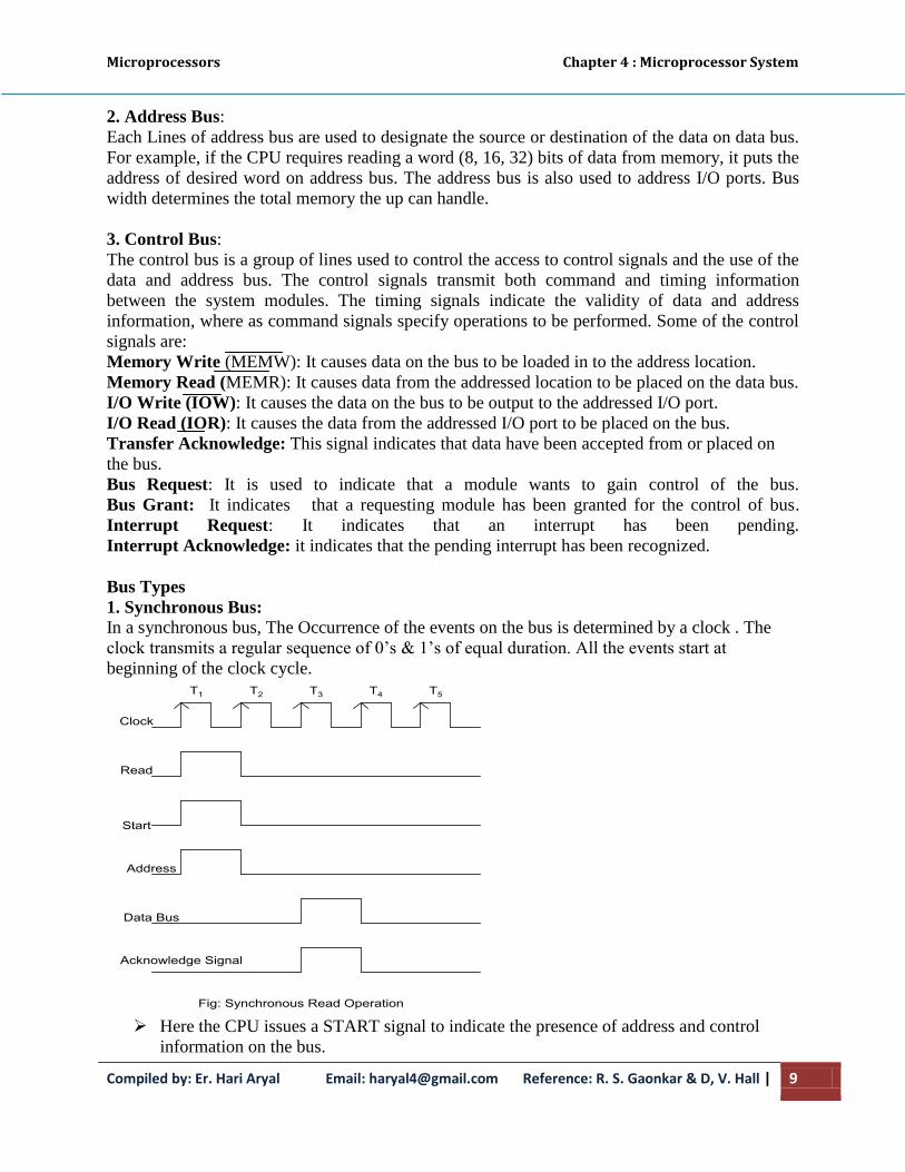
1. Synchronous Bus: In a synchronous bus, The Occurrence of the events on the bus is determined by a clock . The
clock transmits a regular sequence of 0’s & 1’s of equal duration. All the events start at
beginning of the clock cycle.
Here the CPU issues a START signal to indicate the presence of address and control
information on the bus.
Microprocessors Chapter 4 : Microprocessor System
Compiled by: Er. Hari Aryal Email: [email protected] Reference: R. S. Gaonkar & D, V. Hall | 10
Then it issues the memory read signal and places the memory address on the address bus.
The addressed memory module recognizes the address and after a delay of one clock
cycle it places the data and acknowledgment signal on the buses.
In synchronous bus, all devices are tied to a fixed rate, and hence the system can not take
advantage of device performance but it is easy to implement.
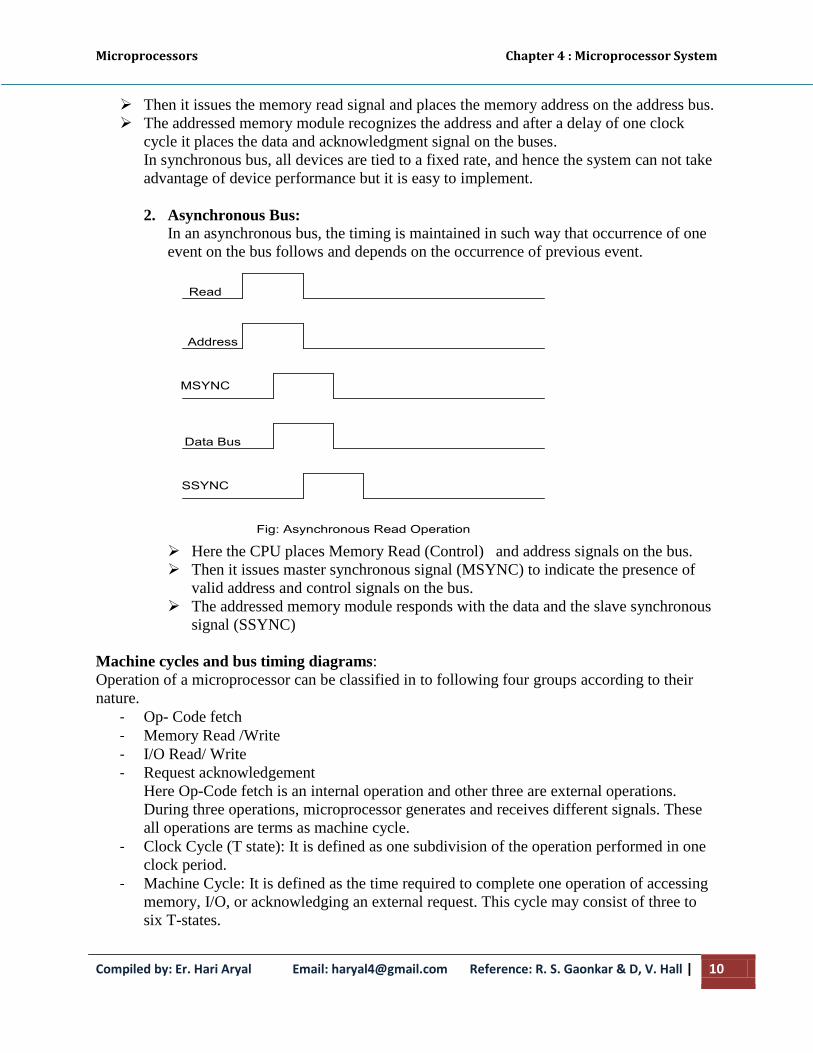
2. Asynchronous Bus:
In an asynchronous bus, the timing is maintained in such way that occurrence of one
event on the bus follows and depends on the occurrence of previous event.
Here the CPU places Memory Read (Control) and address signals on the bus.
Then it issues master synchronous signal (MSYNC) to indicate the presence of
valid address and control signals on the bus.
The addressed memory module responds with the data and the slave synchronous
signal (SSYNC)
Machine cycles and bus timing diagrams:
Operation of a microprocessor can be classified in to following four groups according to their
nature.
- Op- Code fetch
- Memory Read /Write
- I/O Read/ Write
- Request acknowledgement
Here Op-Code fetch is an internal operation and other three are external operations.
During three operations, microprocessor generates and receives different signals. These
all operations are terms as machine cycle.
- Clock Cycle (T state): It is defined as one subdivision of the operation performed in one
clock period.
- Machine Cycle: It is defined as the time required to complete one operation of accessing
memory, I/O, or acknowledging an external request. This cycle may consist of three to
six T-states.
Microprocessors Chapter 4 : Microprocessor System
Compiled by: Er. Hari Aryal Email: [email protected] Reference: R. S. Gaonkar & D, V. Hall | 11
- Instruction Cycle: It is defined as the time required completing the execution of an
instruction. The 8085 instruction cycle consists of one to six machine cycles or one to six
operations.
Op-Code fetch Machine Cycle
The first operation in any instruction is Op-Code fetch, The microprocessor needs to get(fetch)
this machine code from the memory register where it is stored before the microprocessor can
begin to execute the instruction.
Let’s consider the instruction MOV C, A stored at memory location 2005H. The Op-Code for the
instruction is 4FH and Op-Code fetch cycle is of 4 clock cycles.
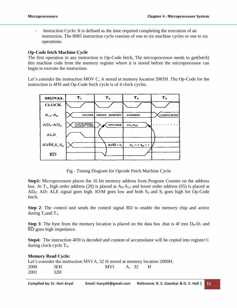
Fig - Timing Diagram for Opcode Fetch Machine Cycle
Step1: Microprocessor places the 16 bit memory address from Program Counter on the address
bus. At T1, high order address (20) is placed at A8-A15 and lower order address (05) is placed at
AD0- AD7 ALE signal goes high. IO/M goes low and both S0 and Sl goes high for Op-Code
fetch.
Step 2: The control unit sends the control signal RD to enable the memory chip and active
during T2and T3.
Step 3: The byte from the memory location is placed on the data bus .that is 4f into D0-D7 and
RD goes high impedance.
Step4: The instruction 4FH is decoded and content of accumulator will be copied into register C
during clock cycle T4.
Memory Read Cycle: Let’s consider the instruction MVI A, 32 H stored at memory location 2000H.
2000 3EH MVI A, 32 H
2001 32H

Microprocessors Chapter 4 : Microprocessor System
Compiled by: Er. Hari Aryal Email: [email protected] Reference: R. S. Gaonkar & D, V. Hall | 12
Here two machine cycles are presented, first is Op-Code fetch which consists of 4 clock cycles
and second is memory read consist of 4 clock cycle.
Fig - Timing Diagram for Memory Read Machine Cycle
Step 1 : First machine cycle (Op-Code fetch ) is identical for timing diagram of Op-Code fetch
cycle.
Step 2: After completion of Op-Code fetch cycle, 8085 places the address 2001 on the address
bus and increments PC to 2002H. ALE is asserted high IO/M =0, S1=1, S0=0 for memory read
cycle. When RD =0, memory places the data byte 32H on the dada bus.
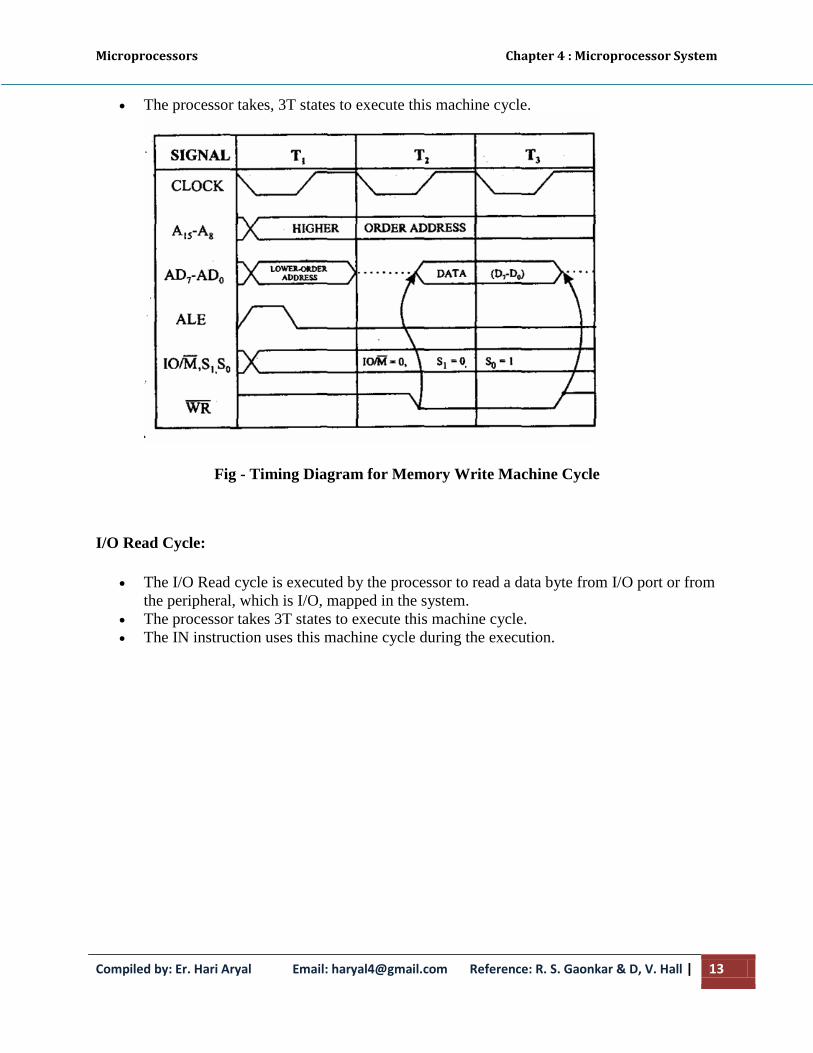
Memory Write Machine:
The memory write machine cycle is executed by the processor to write a data byte in a
memory location.
Microprocessors Chapter 4 : Microprocessor System
Compiled by: Er. Hari Aryal Email: [email protected] Reference: R. S. Gaonkar & D, V. Hall | 13
The processor takes, 3T states to execute this machine cycle.
Fig - Timing Diagram for Memory Write Machine Cycle
I/O Read Cycle:
The I/O Read cycle is executed by the processor to read a data byte from I/O port or from
the peripheral, which is I/O, mapped in the system.
The processor takes 3T states to execute this machine cycle.
The IN instruction uses this machine cycle during the execution.
Microprocessors Chapter 4 : Microprocessor System
Compiled by: Er. Hari Aryal Email: [email protected] Reference: R. S. Gaonkar & D, V. Hall | 14
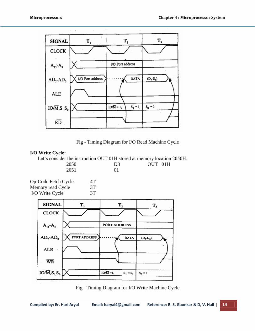
Fig - Timing Diagram for I/O Read Machine Cycle
I/O Write Cycle:
Let’s consider the instruction OUT 01H stored at memory location 2050H.
2050 D3 OUT 01H
2051 01
Op-Code Fetch Cycle 4T
Memory read Cycle 3T
I/O Write Cycle 3T
Fig - Timing Diagram for I/O Write Machine Cycle
Microprocessors Chapter 4 : Microprocessor System
Compiled by: Er. Hari Aryal Email: [email protected] Reference: R. S. Gaonkar & D, V. Hall | 15
Step 1: In Machine Cycle M1, the microprocessor sends RD control signal which is combined
with IO/ M to generate the MEMR signal and processor fetches instruction code D3 using the
data bus.
Step 2: In 2nd
Machine Cycle M2, the 8085 microprocessor places the next address 2051 on the
address bus and gets the device address 01H via data bus.
Step 3: In machine Cycle M3, the 8085 places device address 01H on low order as well as high
order address bus. IO/ M goes high for IO and accumulator content are placed on Data bus which
are to be written into the selected output port.
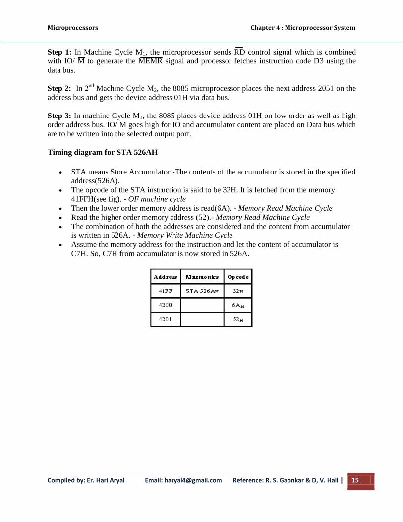
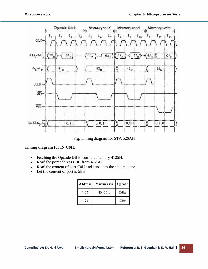
Timing diagram for STA 526AH
STA means Store Accumulator -The contents of the accumulator is stored in the specified
address(526A).
The opcode of the STA instruction is said to be 32H. It is fetched from the memory
41FFH(see fig). - OF machine cycle
Then the lower order memory address is read(6A). - Memory Read Machine Cycle
Read the higher order memory address (52).- Memory Read Machine Cycle
The combination of both the addresses are considered and the content from accumulator
is written in 526A. - Memory Write Machine Cycle
Assume the memory address for the instruction and let the content of accumulator is
C7H. So, C7H from accumulator is now stored in 526A.
Microprocessors Chapter 4 : Microprocessor System
Compiled by: Er. Hari Aryal Email: [email protected] Reference: R. S. Gaonkar & D, V. Hall | 16
Fig. Timing diagram for STA 526AH
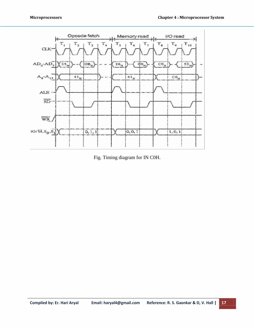
Timing diagram for IN C0H.
Fetching the Opcode DBH from the memory 4125H.
Read the port address C0H from 4126H.
Read the content of port C0H and send it to the accumulator.
Let the content of port is 5EH.
Microprocessors Chapter 4 : Microprocessor System
Compiled by: Er. Hari Aryal Email: [email protected] Reference: R. S. Gaonkar & D, V. Hall | 17
Fig. Timing diagram for IN C0H.

Microprocessors Chapter 4 : Microprocessor System
Compiled by: Er. Hari Aryal Email: [email protected] Reference: R. S. Gaonkar & D, V. Hall | 18
Timing diagram for MVI B, 43H.
Fetching the Opcode 06H from the memory 2000H. (OF machine cycle)
Read (move) the data 43H from memory 2001H. (memory read)
Timing diagram for INR M
Fetching the Opcode 34H from the memory 4105H. (OF cycle)
Let the memory address (M) be 4250H. (MR cycle -To read Memory address and data)
Let the content of that memory is 12H.
Increment the memory content from 12H to 13H. (MW machine cycle)

Microprocessors Chapter 4 : Microprocessor System
Compiled by: Er. Hari Aryal Email: [email protected] Reference: R. S. Gaonkar & D, V. Hall | 19
Read and write bus timing of 8086 microprocessor
• The working of the minimum mode configuration system can be better described in terms
of the timing diagrams rather than qualitatively describing the operations.
• The op-code fetch and read cycles are similar. Hence the timing diagram can be
categorized in two parts, the first is the timing diagram for read cycle and the second is
the timing diagram for write cycle.
• The read cycle begins in T1 with the assertion of address latch enable (ALE) signal and
also M / IO signal. During the negative going edge of this signal, the valid address is
latched on the local bus.
• The BHE and A0 signals address low, high or both bytes. From T1 to T4 , the M/IO
signal indicates a memory or I/O operation.
• At T2, the address is removed from the local bus and is sent to the output. The bus is then
tri-stated. The read (RD) control signal is also activated in T2.
• The read (RD) signal causes the address device to enable its data bus drivers. After RD
goes low, the valid data is available on the data bus.
• The addressed device will drive the READY line high. When the processor returns the
read signal to high level, the addressed device will again tristate its bus drivers

Microprocessors Chapter 4 : Microprocessor System
Compiled by: Er. Hari Aryal Email: [email protected] Reference: R. S. Gaonkar & D, V. Hall | 20
Write cycle timing diagram for minimum mode operation
• A write cycle also begins with the assertion of ALE and the emission of the address. The
M/IO signal is again asserted to indicate a memory or I/O operation. In T2, after sending
the address in T1, the processor sends the data to be written to the addressed location.
• The data remains on the bus until middle of T4 state. The WR becomes active at the
beginning of T2 (unlike RD is somewhat delayed in T2 to provide time for floating).
• The BHE and A0 signals are used to select the proper byte or bytes of memory or I/O
word to be read or write.
• The M/IO, RD and WR signals indicate the type of data transfer as specified in table
below.
Microprocessors Chapter 4 : Microprocessor System
Compiled by: Er. Hari Aryal Email: [email protected] Reference: R. S. Gaonkar & D, V. Hall | 21
Memory Read Timing Diagram in Maximum Mode of 8086

Microprocessors Chapter 4 : Microprocessor System
Compiled by: Er. Hari Aryal Email: [email protected] Reference: R. S. Gaonkar & D, V. Hall | 22
Memory Write Timing in Maximum mode of 8086
Memory devices:
Microprocessors Chapter 4 : Microprocessor System
Compiled by: Er. Hari Aryal Email: [email protected] Reference: R. S. Gaonkar & D, V. Hall | 23
Memory is an essential component of the microcomputer system. It is used to store both
instructions and data. It is used to store both instructions and data. Memory is made up of
registers and the number of bits stored in a register is called memory word .Memory word is
identified by an address .If microprocessor uses 16 bit address , then there will be maximum of
216
= 65536 memory addresses ranging from 0000H to FFFFH.
There are various types of memory which can be classified in to two main groups i.e. Primary
memory and Secondary memory.
1. Primary Memory:
It is the memory used by microprocessor to execute programs. The microprocessor can access
only those items that are stored in this memory. Hence, all data and program must be within
primary memory prior to its execution. Primary memory is much larger than processer memory
that is included in the microprocessor chip.
Primary memory is divided in to two groups.
i. R/W Memory (RAM )
Microprocessor can read for and write into this memory .This memory is used for
information that are likely to be altered such as writing program or receiving data. This
memory is volatile i.e. the content will be lost if the power is turned off and commonly
known as RAM, RAM are basically of two types.
A. Static RAM (SRAM)
This memory is made up of flip flops and it stores bit as voltage. A single flip flop
stores binary data either 1 or 0. Each flip flop is called storage cell. Each cell
requires six transistors. Therefore, the memory chip has low density but high
speed. This memory is more expensive and consumes more power.
B. Dynamic RAM (DRAM)
This memory is made up of MOS transistor gates and it stores the bit as charge.
The advantage of DRAM are it has high density, low power consumption and
cheaper than SRAM. But the bit information leaks therefore needs to be rewritten
again every few milliseconds. It is called refreshing the memory and requires extra
circuitry to do this. It is slower than SRAM.
Read Only Memory (ROM):
ROM contains a permanent pattern of data that cannot be changed. It is non volatile that
is no power source is required to maintain the bit values in memory. ROM are basically
of 5 types.
A. Masked ROM: A bit pattern is permanently recorded by the manufactures during
production.
B. Programmable ROM: In this ROM, a bit pattern may be written into only once and
the writing process is performed electrically. That may be performed by a supplier or
customer.
C. Erasable PROM (EPROM):
This memory stores a bit in the form of charge by using EPROM programmer which
applies high voltage to charge the gate .Information can be erased by exposing ultra
Microprocessors Chapter 4 : Microprocessor System
Compiled by: Er. Hari Aryal Email: [email protected] Reference: R. S. Gaonkar & D, V. Hall | 24
violet radiation. It is reusable. The disadvantages are :(i) it must be taken out off circuit
to erase it (ii). The entire chip must be erased (iii) the erasing process takes 15 to 20
minutes.
D. Electrically Erasable PROM(EEPROM):
It is functionally same as EPROM except that information can be altered by using
electrical signal at the register level rather than erasing all the information. It is
expensive compared to EPROM and flash and can be erased in 10 ms.
E. Flash Memory:
It is variation of EPROM. The difference is that EPROM can be erased in register
level but flash memory must be erased in register level but flash memory must be
erased in its entirety or at block level.
2. Secondary memory
The devices that provide backup storage are called secondary memory. It includes
serial access type such as magnetic disks and random access type such as magnetic
disks. It is nonvolatile memory.
Performance of memory:
1. Access time (ta):
Read access time: It is the average time required to read the unit of information
from memory.
Write access time: It is the average time required to write the unit of information
on memory.
Access rate (ra) = /ta
2. Cycle time (tc):
It is the average time that lapses between two successive read operation .
Cycle rate (rc)= bandwidth = 1/tc
Access modes of memory:
1. Random access: In random access mode, the ta is independent of the
location from which the data is accessed like MOS memory.
2. Sequential access: In that mode, the ta is dependent of the location form
which the data is accessed like magnetic type.
3. Semi random-access: the semi random access combines these two. for
eg. In magnetic disk, any track can be accessed at random. But the access within the
truck must be in serial fashion.
The Memory Hierarchy
Capacity, cost and speed of different types of memory play a vital role while designing a
memory system for computers.
If the memory has larger capacity, more application will get space to run smoothly.
It's better to have fastest memory as far as possible to achieve a greater performance.
Moreover for the practical system, the cost should be reasonable.
There is a tradeoff between these three characteristics cost, capacity and access time. One
cannot achieve all these quantities in same memory module because
Microprocessors Chapter 4 : Microprocessor System
Compiled by: Er. Hari Aryal Email: [email protected] Reference: R. S. Gaonkar & D, V. Hall | 25
If capacity increases, access time increases (slower) and due to which cost per bit
decreases.
If access time decreases (faster), capacity decreases and due to which cost per bit
increases.
The designer tries to increase capacity because cost per bit decreases and the more
application program can be accommodated. But at the same time, access time increases
and hence decreases the performance.
So the best idea will be to use memory hierarchy.
Memory Hierarchy is to obtain the highest possible access speed while minimizing the
total cost of the memory system.
Not all accumulated information is needed by the CPU at the same time.
Therefore, it is more economical to use low-cost storage devices to serve as a backup for
storing the information that is not currently used by CPU
The memory unit that directly communicate with CPU is called the main memory
Devices that provide backup storage are called auxiliary memory
The memory hierarchy system consists of all storage devices employed in a computer
system from the slow by high-capacity auxiliary memory to a relatively faster main
memory, to an even smaller and faster cache memory
The main memory occupies a central position by being able to communicate directly with
the CPU and with auxiliary memory devices through an I/O processor
A special very-high-speed memory called cache is used to increase the speed of
processing by making current programs and data available to the CPU at a rapid rate
CPU logic is usually faster than main memory access time, with the result that processing
speed is limited primarily by the speed of main memory
The cache is used for storing segments of programs currently being executed in the CPU
and temporary data frequently needed in the present calculations
The memory hierarchy system consists of all storage devices employed in a computer
system from slow but high capacity auxiliary memory to a relatively faster cache memory
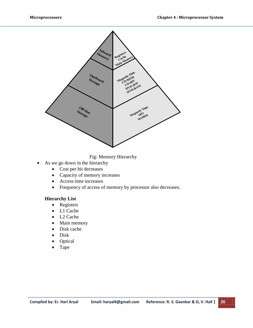
accessible to high speed processing logic. The figure below illustrates memory hierarchy.
Microprocessors Chapter 4 : Microprocessor System
Compiled by: Er. Hari Aryal Email: [email protected] Reference: R. S. Gaonkar & D, V. Hall | 26
Fig: Memory Hierarchy
As we go down in the hierarchy
Cost per bit decreases
Capacity of memory increases
Access time increases
Frequency of access of memory by processor also decreases.
Hierarchy List
Registers
L1 Cache
L2 Cache
Main memory
Disk cache
Disk
Optical
Tape
Microprocessors Chapter 4 : Microprocessor System
Compiled by: Er. Hari Aryal Email: [email protected] Reference: R. S. Gaonkar & D, V. Hall | 27
Address decoding:
Microprocessor is connected with memory and I/O devices via common address
and data bus. Only one device can send data at a time and other devices can only receive
that data. If more than one device sends data at the same time, the data gets garbled. In
order to avoid this situation, ensuring that the proper device gets addressed at proper
time, the technique called address decoding is used.
In address decoding method, all devices like memory blocks, I/O units etc. are
assigned with a specific address. The address of the device is determined from the way in
which the address lines are used to derive a special device selection signal k/a chip select
(CS). If the microprocessor has to write or to read from a device, the CS signal to that
block should be enabled and the address decoding circuit must ensure that CS signal to
other devices are not activated.
Depending upon the no. of address lines used to generate chip select signal for the
device, the address decoding is classified as:
1. I/O mapped I/O
In this method, a device is identified with an 8 bit address and operated by I/O related
functions IN and OUT for that IO/M =1. Since only 8bit address is used, at most 256
bytes can be identified uniquely. Generally low order address bits A0-A7 are used and
upper bits A8-A15 are considered don’t care. Usually I/O mapped I/O is used to map
devices like 8255A, 8251A etc.
2. Memory mapped I/O
In this method , a device is identified with 16 bit address and enabled memory related
functions such as STA , LDA for which IO/M =0, here chip select signal of each
device is derived from 16 bit address lines thus total addressing capability is 64K
bytes . Usually memory mapped I/O is used to map memories like RAM, ROM etc.
Depending on the address that are allocated to the device the address decoding are
categorized in the following two groups.
Microprocessors Chapter 4 : Microprocessor System
Compiled by: Er. Hari Aryal Email: [email protected] Reference: R. S. Gaonkar & D, V. Hall | 28
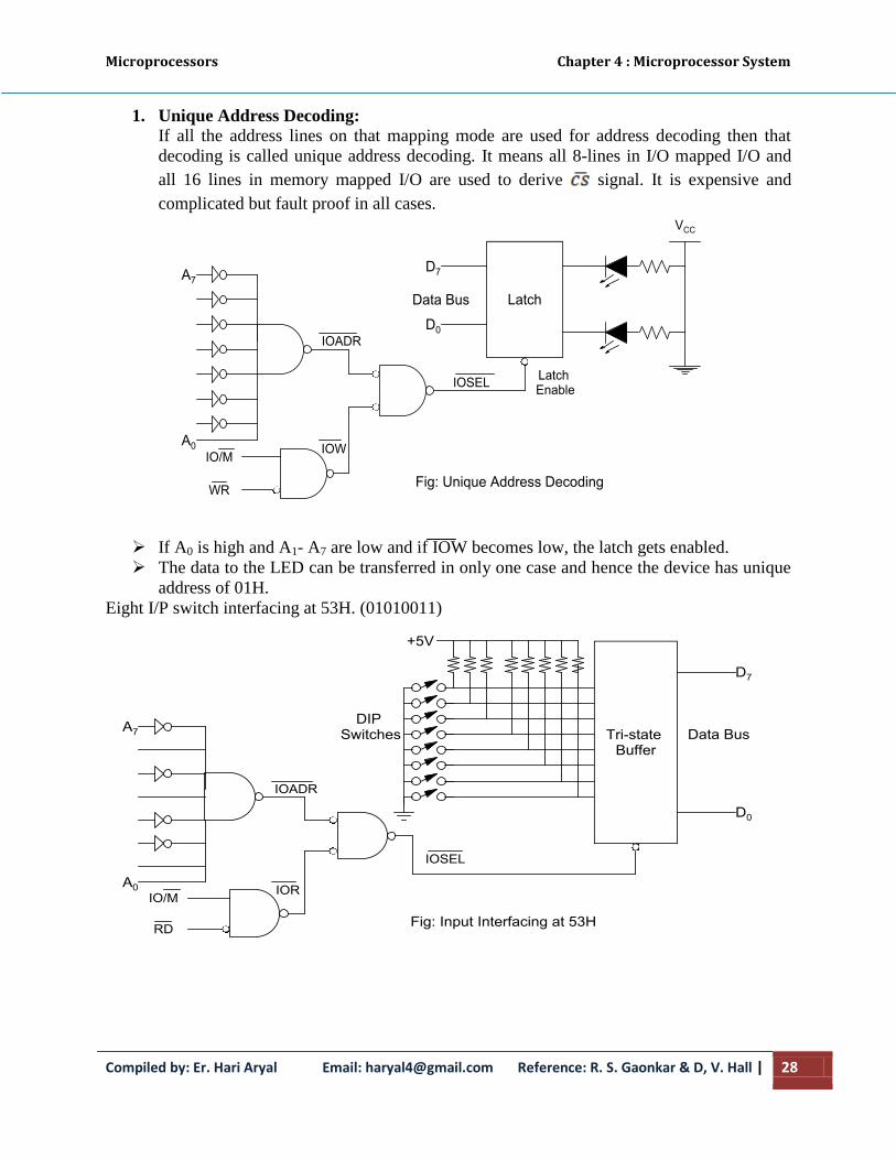
1. Unique Address Decoding:
If all the address lines on that mapping mode are used for address decoding then that
decoding is called unique address decoding. It means all 8-lines in I/O mapped I/O and
all 16 lines in memory mapped I/O are used to derive signal. It is expensive and
complicated but fault proof in all cases.
If A0 is high and A1- A7 are low and if IOW becomes low, the latch gets enabled.
The data to the LED can be transferred in only one case and hence the device has unique
address of 01H.
Eight I/P switch interfacing at 53H. (01010011)
Microprocessors Chapter 4 : Microprocessor System
Compiled by: Er. Hari Aryal Email: [email protected] Reference: R. S. Gaonkar & D, V. Hall | 29
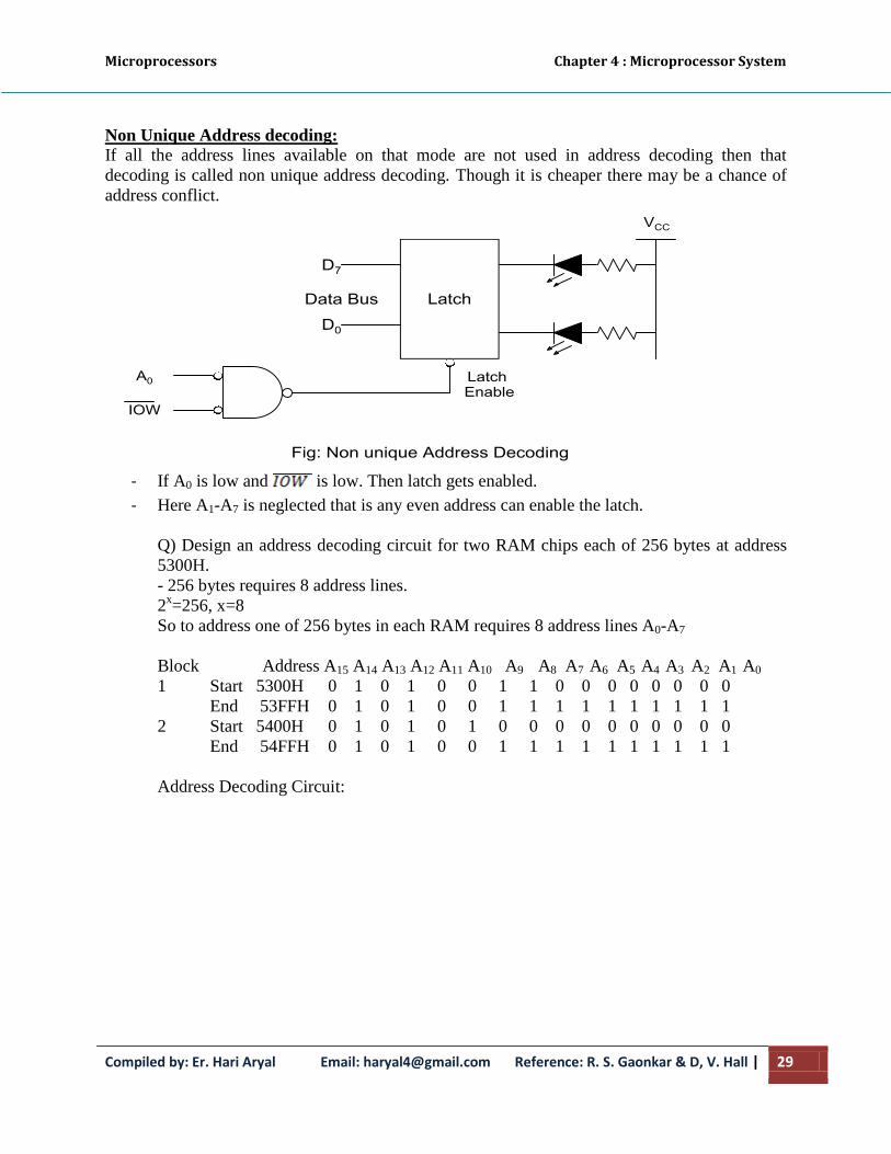
Non Unique Address decoding:
If all the address lines available on that mode are not used in address decoding then that
decoding is called non unique address decoding. Though it is cheaper there may be a chance of
address conflict.
- If A0 is low and is low. Then latch gets enabled.
- Here A1-A7 is neglected that is any even address can enable the latch.
Q) Design an address decoding circuit for two RAM chips each of 256 bytes at address
5300H.
- 256 bytes requires 8 address lines.
2x=256, x=8
So to address one of 256 bytes in each RAM requires 8 address lines A0-A7
Block Address A15 A14 A13 A12 A11 A10 A9 A8 A7 A6 A5 A4 A3 A2 A1 A0
1 Start 5300H 0 1 0 1 0 0 1 1 0 0 0 0 0 0 0 0
End 53FFH 0 1 0 1 0 0 1 1 1 1 1 1 1 1 1 1
2 Start 5400H 0 1 0 1 0 1 0 0 0 0 0 0 0 0 0 0
End 54FFH 0 1 0 1 0 0 1 1 1 1 1 1 1 1 1 1
Address Decoding Circuit:
Microprocessors Chapter 4 : Microprocessor System
Compiled by: Er. Hari Aryal Email: [email protected] Reference: R. S. Gaonkar & D, V. Hall | 30
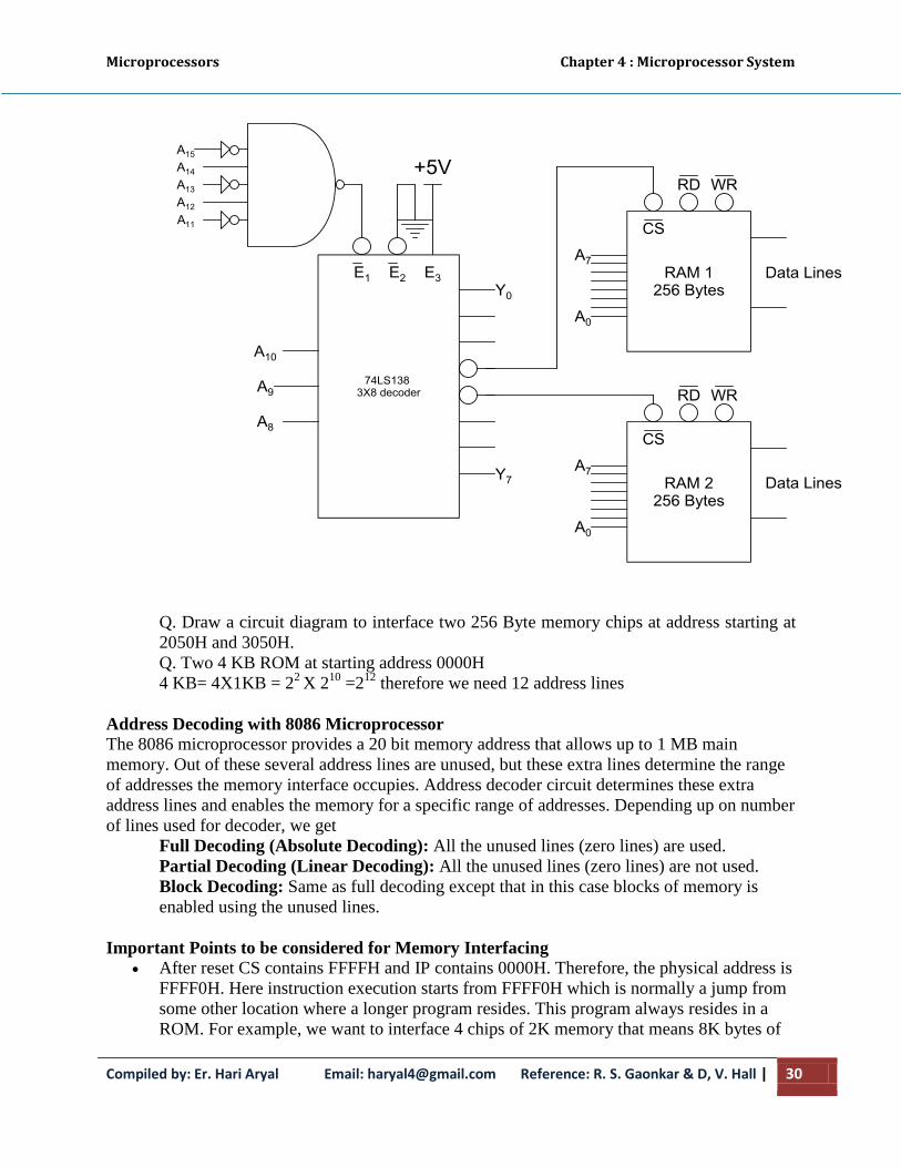
Q. Draw a circuit diagram to interface two 256 Byte memory chips at address starting at
2050H and 3050H.
Q. Two 4 KB ROM at starting address 0000H
4 KB= 4X1KB = 22
X 210
=212
therefore we need 12 address lines
Address Decoding with 8086 Microprocessor
The 8086 microprocessor provides a 20 bit memory address that allows up to 1 MB main
memory. Out of these several address lines are unused, but these extra lines determine the range
of addresses the memory interface occupies. Address decoder circuit determines these extra
address lines and enables the memory for a specific range of addresses. Depending up on number
of lines used for decoder, we get
Full Decoding (Absolute Decoding): All the unused lines (zero lines) are used.
Partial Decoding (Linear Decoding): All the unused lines (zero lines) are not used.
Block Decoding: Same as full decoding except that in this case blocks of memory is
enabled using the unused lines.
Important Points to be considered for Memory Interfacing
After reset CS contains FFFFH and IP contains 0000H. Therefore, the physical address is
FFFF0H. Here instruction execution starts from FFFF0H which is normally a jump from
some other location where a longer program resides. This program always resides in a
ROM. For example, we want to interface 4 chips of 2K memory that means 8K bytes of
Microprocessors Chapter 4 : Microprocessor System
Compiled by: Er. Hari Aryal Email: [email protected] Reference: R. S. Gaonkar & D, V. Hall | 31
memory requires 13 address lines A0 to A12. So, 8K means 01FFFH bytes, therefore
EPROM address starts from FFFFFH – 01FFFH = FE000H.
Since ROMs and EPROMs are read-only devices, A0 and BHE’ are not required to be
part of the chip enable/select decoding. The 8086 address lines must be connected to the
ROM/EPROM chip starting with A1 and higher to all the address lines of the
ROM/EPROM chips. The 8086 unused address lines can be used as chip enable/select
decoding.
Since static RAMs are read/write memories, both A0 and BHE’ must be included in the
chip select/enable decoding of the devices and write timing must be considered in the
compatibility analysis.
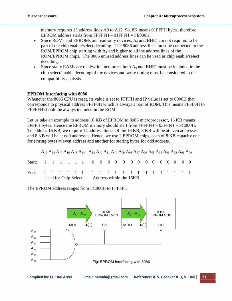
EPROM Interfacing with 8086
Whenever the 8086 CPU is reset, its value is set to FFFFH and IP value is set to 0000H that
corresponds to physical address FFFF0H which is always a part of ROM. This means FFFF0H to
FFFFFH should be always included in the ROM.
Let us take an example to address 16 KB of EPROM to 8086 microprocessor, 16 KB means
3FFFH bytes. Hence the EPROM memory should start from FFFFFH – 03FFFH = FC000H.
To address 16 KB, we require 14 address lines. Of the 16 KB, 8 KB will be at even addresses
and 8 KB will be at odd addresses. Hence, we use 2 EPROM chips, each of 8 KB capacity one
for storing bytes at even address and another for storing bytes for odd address.
A19 A18 A17 A16 A15 A14 A13 A12 A11 A10 A09 A08 A07 A06 A05 A04 A03 A02 A01 A00
Start: 1 1 1 1 1 1 0 0 0 0 0 0 0 0 0 0 0 0 0 0
End: 1 1 1 1 1 1 1 1 1 1 1 1 1 1 1 1 1 1 1 1
Used for Chip Select Address within the 16KB
The EPROM address ranges from FC000H to FFFFFH
Microprocessors Chapter 4 : Microprocessor System
Compiled by: Er. Hari Aryal Email: [email protected] Reference: R. S. Gaonkar & D, V. Hall | 32
A0 and BHE’ is not used for interfacing of EPROM. Both the 8 KB EPROM chips are selected
whenever any address in the range FC000H – FFFFFH comes on the address bus.
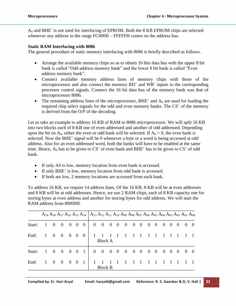
Static RAM Interfacing with 8086
The general procedure of static memory interfacing with 8086 is briefly described as follows.
Arrange the available memory chips so as to obtain 16 bits data bus with the upper 8 bit
bank is called “Odd address memory bank” and the lower 8 bit bank is called “Even
address memory bank”.
Connect available memory address lines of memory chips with those of the
microprocessor and also connect the memory RD’ and WR’ inputs to the corresponding
processor control signals. Connect the 16 bit data bus of the memory bank was that of
microprocessor 8086.
The remaining address lines of the microprocessor, BHE’ and A0 are used for loading the
required chip select signals for the odd and even memory banks. The CS’ of the memory
is derived from the O/P of the decoding.
Let us take an example to address 16 KB of RAM to 8086 microprocessor. We will split 16 KB
into two blocks each of 8 KB one of even addressed and another of odd addressed. Depending
upon the bit on A0, either the even or odd bank will be selected. If A0 = 0, the even bank is
selected. Now the BHE’ signal will be 0 whenever a byte or a word is being accessed at odd
address. Also for an even addressed word, both the banks will have to be enabled at the same
time. Hence, A0 has to be given to CS’ of even bank and BHE’ has to be given to CS’ of odd
bank.
If only A0 is low, memory location from even bank is accessed.
If only BHE’ is low, memory location from odd bank is accessed.
If both are low, 2 memory locations are accessed from each bank.
To address 16 KB, we require 14 address lines. Of the 16 KB, 8 KB will be at even addresses
and 8 KB will be at odd addresses. Hence, we use 2 RAM chips, each of 8 KB capacity one for
storing bytes at even address and another for storing bytes for odd address. We will start the
RAM address from 80000H.
A19 A18 A17 A16 A15 A14 A13 A12 A11 A10 A09 A08 A07 A06 A05 A04 A03 A02 A01 A00
Start: 1 0 0 0 0 0 0 0 0 0 0 0 0 0 0 0 0 0 0 0
End: 1 0 0 0 0 0 1 1 1 1 1 1 1 1 1 1 1 1 1 1
Block A
Start: 1 0 0 0 0 1 0 0 0 0 0 0 0 0 0 0 0 0 0 0
End: 1 0 0 0 0 1 1 1 1 1 1 1 1 1 1 1 1 1 1 1
Block B
Microprocessors Chapter 4 : Microprocessor System
Compiled by: Er. Hari Aryal Email: [email protected] Reference: R. S. Gaonkar & D, V. Hall | 33
As a good and efficient interfacing practice, the address map of the system should be continuous
as far as possible i.e. these should be no windows and no feedback space should be allowed. A
memory location should have a single address corresponding to it i.e. absolute decoding should
be preferred.
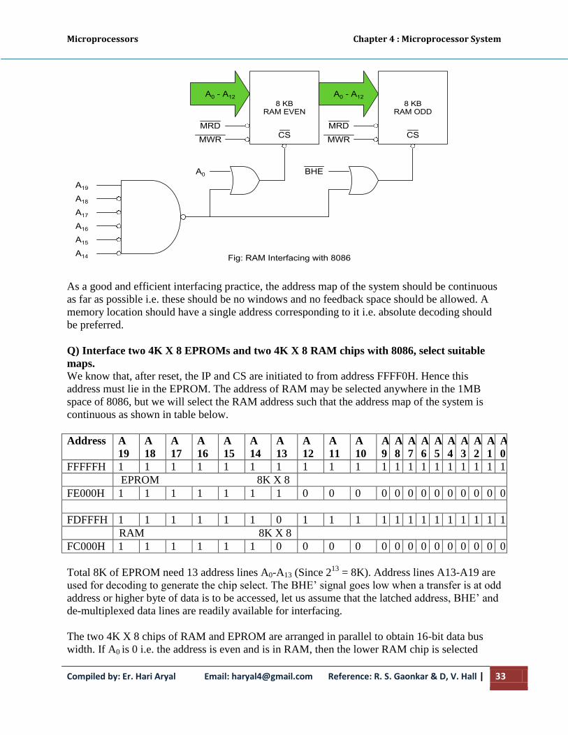
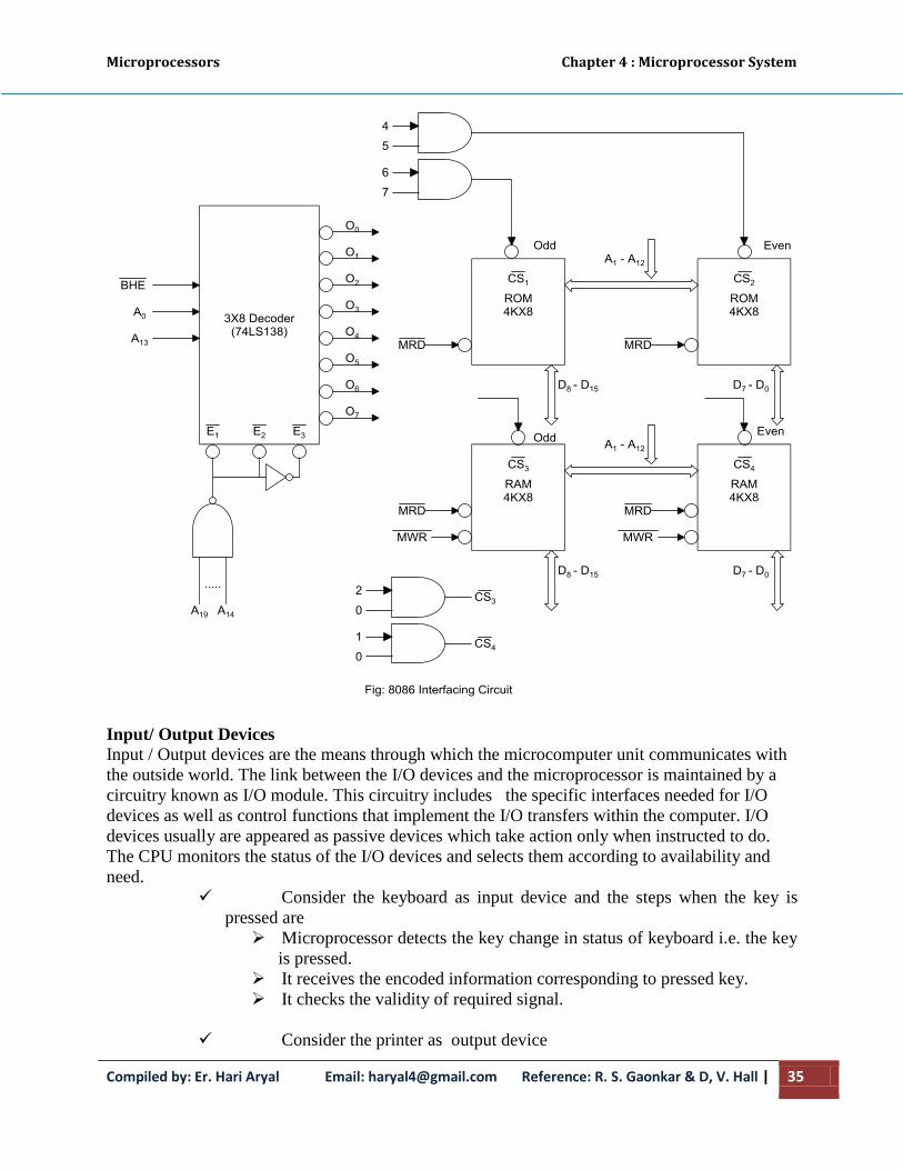
Q) Interface two 4K X 8 EPROMs and two 4K X 8 RAM chips with 8086, select suitable
maps.
We know that, after reset, the IP and CS are initiated to from address FFFF0H. Hence this
address must lie in the EPROM. The address of RAM may be selected anywhere in the 1MB
space of 8086, but we will select the RAM address such that the address map of the system is
continuous as shown in table below.
Address A
19
A
18
A
17
A
16
A
15
A
14
A
13
A
12
A
11
A
10
A
9
A
8
A
7
A
6
A
5
A
4
A
3
A
2
A
1
A
0
FFFFFH 1 1 1 1 1 1 1 1 1 1 1 1 1 1 1 1 1 1 1 1
EPROM 8K X 8
FE000H 1 1 1 1 1 1 1 0 0 0 0 0 0 0 0 0 0 0 0 0
FDFFFH 1 1 1 1 1 1 0 1 1 1 1 1 1 1 1 1 1 1 1 1
RAM 8K X 8
FC000H 1 1 1 1 1 1 0 0 0 0 0 0 0 0 0 0 0 0 0 0
Total 8K of EPROM need 13 address lines A0-A13 (Since 213
= 8K). Address lines A13-A19 are
used for decoding to generate the chip select. The BHE’ signal goes low when a transfer is at odd
address or higher byte of data is to be accessed, let us assume that the latched address, BHE’ and
de-multiplexed data lines are readily available for interfacing.
The two 4K X 8 chips of RAM and EPROM are arranged in parallel to obtain 16-bit data bus
width. If A0 is 0 i.e. the address is even and is in RAM, then the lower RAM chip is selected
Microprocessors Chapter 4 : Microprocessor System
Compiled by: Er. Hari Aryal Email: [email protected] Reference: R. S. Gaonkar & D, V. Hall | 34
indicating 8-bit transfer at even address. If A0 is 1 i.e. the address is odd and is in RAM, the
BHE’ goes low, the upper RAM chip is selected further indicating that the 8 bit transfer is at an
odd address. If the selected addresses are in ROM, the respective ROM chips are selected. If at a
time A0 and BHE’ both are zero, both the RAM or ROM chips are selected i.e. the data transfer
is of 16 bits. The selection of chips takes place as shown in table below.
Decoder I/P
Address / BHE’
A2 A1 A0 Selection /
Comment A13 A0 BHE’
Word transfer on
D0-D15
0 0 0 Even and Odd
address in RAM
Byte transfer on
D0-D7
0 0 1 Only even
address in RAM
Byte transfer on
D8-D15
0 1 0 Only odd address
in RAM
Word transfer on
D0-D15
1 0 0 Even and Odd
address in ROM
Byte transfer on
D0-D7
1 0 1 Only even
address in ROM
Byte transfer on
D8-D15
1 1 0 Only odd address
in ROM
Microprocessors Chapter 4 : Microprocessor System
Compiled by: Er. Hari Aryal Email: [email protected] Reference: R. S. Gaonkar & D, V. Hall | 35
Input/ Output Devices
Input / Output devices are the means through which the microcomputer unit communicates with
the outside world. The link between the I/O devices and the microprocessor is maintained by a
circuitry known as I/O module. This circuitry includes the specific interfaces needed for I/O
devices as well as control functions that implement the I/O transfers within the computer. I/O
devices usually are appeared as passive devices which take action only when instructed to do.
The CPU monitors the status of the I/O devices and selects them according to availability and
need.
Consider the keyboard as input device and the steps when the key is
pressed are
Microprocessor detects the key change in status of keyboard i.e. the key
is pressed.
It receives the encoded information corresponding to pressed key.
It checks the validity of required signal.
Consider the printer as output device
Microprocessors Chapter 4 : Microprocessor System
Compiled by: Er. Hari Aryal Email: [email protected] Reference: R. S. Gaonkar & D, V. Hall | 36
Here microprocessor checks ideal condition of printer, if ideal then
sends the data to be printed and required command for that.
For interfacing of typical microprocessor to I/O devices such as keyboard, CRT, printer
etc. All need I/O interface circuits which are of mainly two types.
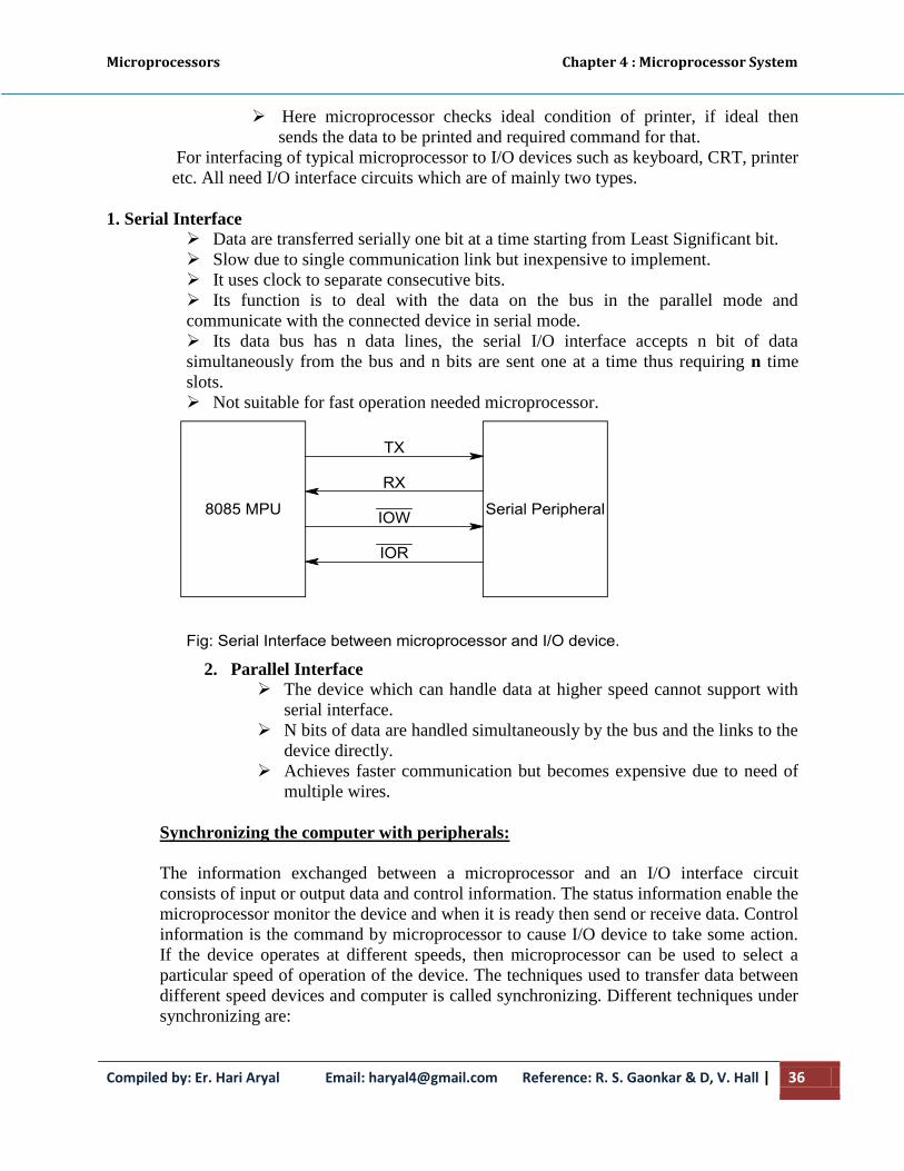
1. Serial Interface
Data are transferred serially one bit at a time starting from Least Significant bit.
Slow due to single communication link but inexpensive to implement.
It uses clock to separate consecutive bits.
Its function is to deal with the data on the bus in the parallel mode and
communicate with the connected device in serial mode.
Its data bus has n data lines, the serial I/O interface accepts n bit of data
simultaneously from the bus and n bits are sent one at a time thus requiring n time
slots.
Not suitable for fast operation needed microprocessor.
2. Parallel Interface
The device which can handle data at higher speed cannot support with
serial interface.
N bits of data are handled simultaneously by the bus and the links to the
device directly.
Achieves faster communication but becomes expensive due to need of
multiple wires.
Synchronizing the computer with peripherals:
The information exchanged between a microprocessor and an I/O interface circuit
consists of input or output data and control information. The status information enable the
microprocessor monitor the device and when it is ready then send or receive data. Control
information is the command by microprocessor to cause I/O device to take some action.
If the device operates at different speeds, then microprocessor can be used to select a
particular speed of operation of the device. The techniques used to transfer data between
different speed devices and computer is called synchronizing. Different techniques under
synchronizing are:

Microprocessors Chapter 4 : Microprocessor System
Compiled by: Er. Hari Aryal Email: [email protected] Reference: R. S. Gaonkar & D, V. Hall | 37
1) Simple I/O
For simple I/O, the buffer switch and latch switches i. e. LED are always connected to
the input and output ports. The devices are always ready to send or receive data.
Here cross line indicate the time for new valid data.
2) Wait Interface( Simple strobe I/O)
In this technique, MP need to wait until the device is ready for the operation.
Consider a simple keyboard consisting of 8 switches connected to a MP through a
parallel interface CKT (Tri-state buffer). The switch is of dip switches. In order to use
this keyboard as an input device the MP should be able to detect that a key has been
activated. This can be done by observing that all the bits are in required order. The
processor should repeatedly read the state of input port until it finds the right order of
bits i.e. at least 1 bit of 8 bits should be 0.
Consider the tri-state A/D converter
- Used to convert analog to digital data which can be read by I/O unit of MP
- When SOC appears 1, I/O unit should ready for reading binary data/digital data.
- When EOC’s status is 1, then I/O unit should stop to read data.
- Strobe signal indicates the time at which data is being activated to transmit.
Microprocessors Chapter 4 : Microprocessor System
Compiled by: Er. Hari Aryal Email: [email protected] Reference: R. S. Gaonkar & D, V. Hall | 38
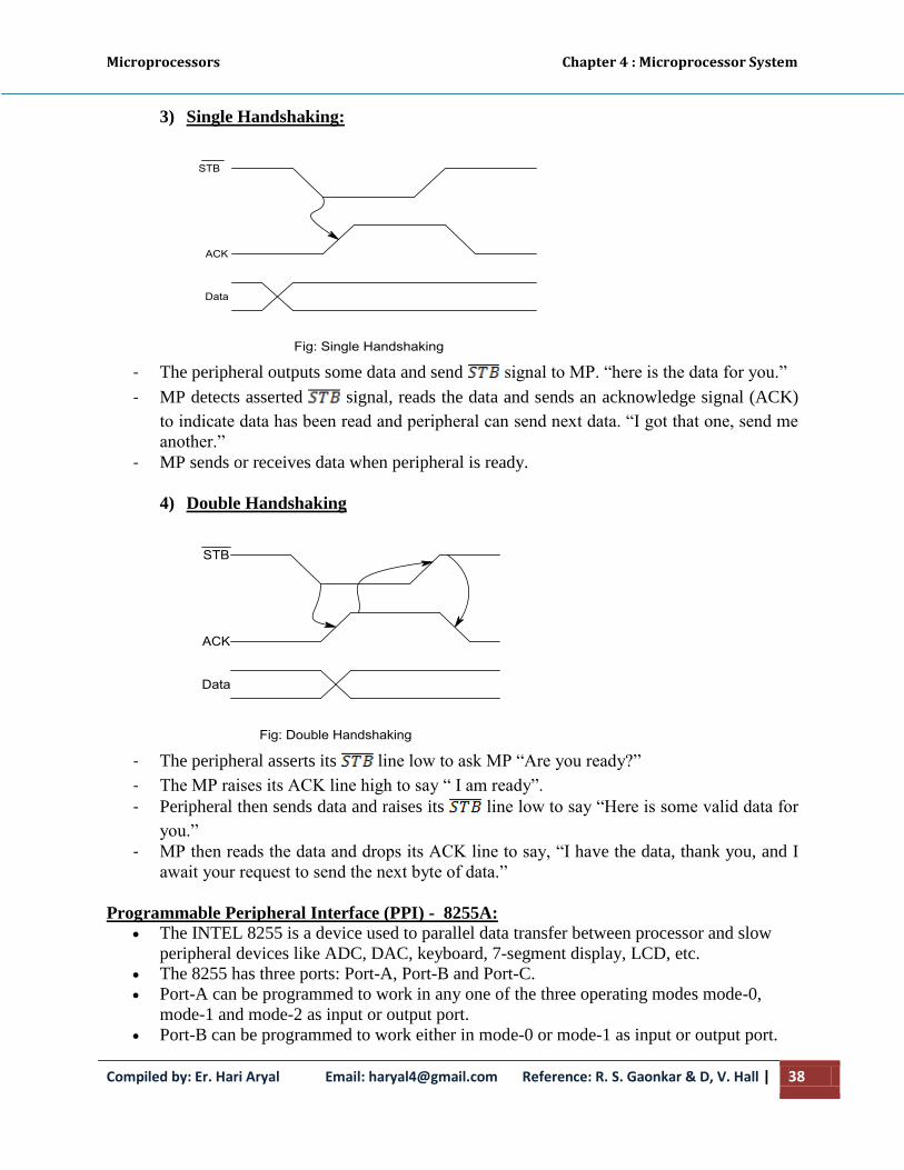
3) Single Handshaking:
- The peripheral outputs some data and send signal to MP. “here is the data for you.”
- MP detects asserted signal, reads the data and sends an acknowledge signal (ACK)
to indicate data has been read and peripheral can send next data. “I got that one, send me
another.”
- MP sends or receives data when peripheral is ready.
4) Double Handshaking
- The peripheral asserts its line low to ask MP “Are you ready?”
- The MP raises its ACK line high to say “ I am ready”.
- Peripheral then sends data and raises its line low to say “Here is some valid data for
you.”
- MP then reads the data and drops its ACK line to say, “I have the data, thank you, and I
await your request to send the next byte of data.”
Programmable Peripheral Interface (PPI) - 8255A:
The INTEL 8255 is a device used to parallel data transfer between processor and slow
peripheral devices like ADC, DAC, keyboard, 7-segment display, LCD, etc.
The 8255 has three ports: Port-A, Port-B and Port-C.
Port-A can be programmed to work in any one of the three operating modes mode-0,
mode-1 and mode-2 as input or output port.
Port-B can be programmed to work either in mode-0 or mode-1 as input or output port.

Microprocessors Chapter 4 : Microprocessor System
Compiled by: Er. Hari Aryal Email: [email protected] Reference: R. S. Gaonkar & D, V. Hall | 39
Port-C (8-pins) has different assignments depending on the mode of port-A and port-B.
If port-A and B are programmed in mode-0, then the port-C can perform any one of the
following functions.
As 8-bit parallel port in mode-0 for input or output.
As two numbers of 4-bit parallel ports in mode-0 for input or output.
The individual pins of port-C can be set or reset for various control
applications.
If port-A is programmed in mode- 1/mode-2 and port-B is programmed in mode-1 then
some of the pins of port-C are used for handshake signals and the remaining pins can be
used as input/ output lines or individually set/reset for control application.
Fig2: Internal Block Diagram of 8255
Key Features of Mode-0,Mode-1 and Mode-2
Mode 0: Ports A and B operate as either inputs or outputs and Port C is divided
into two 4-bit groups either of which can be operated as inputs or outputs
Mode 1: Same as Mode 0 but Port C is used for handshaking and control
Mode 2: Port A is bidirectional (both input and output) and Port C is used for
handshaking. Port B is not used.
The read/write control logic requires six control signals. These signals are given below.
1. RD (low): This control signal enables the read operation. When this signal is low,
the microprocessor reads data from a selected I/O port of the 8255A.
2. WR (low): This control signal enables the write operation. When this signal goes
low, the microprocessor writes into a selected I/O port or the control register.
Microprocessors Chapter 4 : Microprocessor System
Compiled by: Er. Hari Aryal Email: [email protected] Reference: R. S. Gaonkar & D, V. Hall | 40
3. RESET: This is an active high signal. It clears the control register and set all ports
in the input mode.
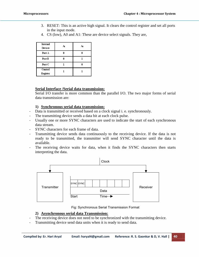
4. CS (low), A0 and A1: These are device select signals. They are,
Serial Interface /Serial data transmission:
Serial I/O transfer is more common than the parallel I/O. The two major forms of serial
data transmission are:
1) Synchronous serial data transmission:
- Data is transmitted or received based on a clock signal i. e. synchronously.
- The transmitting device sends a data bit at each clock pulse.
- Usually one or more SYNC characters are used to indicate the start of each synchronous
data stream.
- SYNC characters for each frame of data.
- Transmitting device sends data continuously to the receiving device. If the data is not
ready to be transmitted, the transmitter will send SYNC character until the data is
available.
- The receiving device waits for data, when it finds the SYNC characters then starts
interpreting the data.
2) Asynchronous serial data Transmission:
- The receiving device does not need to be synchronized with the transmitting device.
- Transmitting device send data units when it is ready to send data.

Microprocessors Chapter 4 : Microprocessor System
Compiled by: Er. Hari Aryal Email: [email protected] Reference: R. S. Gaonkar & D, V. Hall | 41
- Each data unit must contain start and stop bits for indicating beginning and the end of
data unit. And also one parity bit to identify odd or even parity data.
- For e.g. To send ASCII character (7 bit)
- We need: 1 start bit: beginning of data
1 stop bit: End of data
1 Parity bit: even or odd parity
7 or 8 bit character: actual data transferred
Synchronous vs. Asynchronous Data Transmission
Asynchronous Communication
Simple interface (limited data rate, typically < 64 kbps)
Used for connecting: Printer, Terminal, Modem, home connections to the Internet
No clock sent (Tx & Rx have own clocks)
Requires start and stop bits which provides byte timing and increases overhead
Parity often used to validate correct reception.
Independent transmit & receive clocks
Synchronous Communication
Clock sent with data (more configuration options).
Synchronised transmit & receive clocks.
More complex interface (high data rates supported up to ~ 10 Gbps)
Used for: Connections between computer and telephony networks.
Universal Synchronous Asynchronous Receiver Transmitter (USART) – 5251A The 8251A is a programmable serial communication interface chip designed for
synchronous and asynchronous serial data communication.
It supports the serial transmission of data.
The functional block diagram of 825 1A consists five sections. They are:
Read/Write control logic
Transmitter
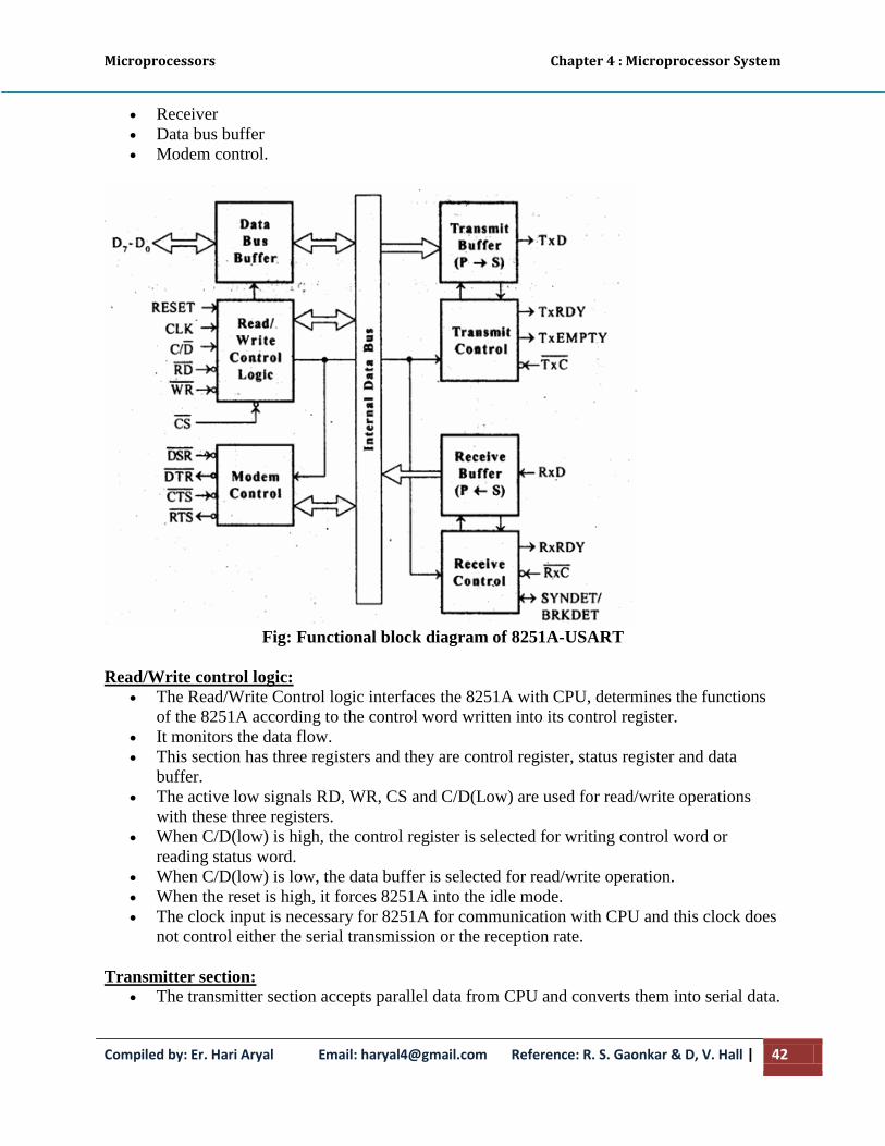
Microprocessors Chapter 4 : Microprocessor System
Compiled by: Er. Hari Aryal Email: [email protected] Reference: R. S. Gaonkar & D, V. Hall | 42
Receiver
Data bus buffer
Modem control.
Fig: Functional block diagram of 8251A-USART
Read/Write control logic:
The Read/Write Control logic interfaces the 8251A with CPU, determines the functions
of the 8251A according to the control word written into its control register.
It monitors the data flow.
This section has three registers and they are control register, status register and data
buffer.
The active low signals RD, WR, CS and C/D(Low) are used for read/write operations
with these three registers.
When C/D(low) is high, the control register is selected for writing control word or
reading status word.
When C/D(low) is low, the data buffer is selected for read/write operation.
When the reset is high, it forces 8251A into the idle mode.
The clock input is necessary for 8251A for communication with CPU and this clock does
not control either the serial transmission or the reception rate.
Transmitter section:
The transmitter section accepts parallel data from CPU and converts them into serial data.

Microprocessors Chapter 4 : Microprocessor System
Compiled by: Er. Hari Aryal Email: [email protected] Reference: R. S. Gaonkar & D, V. Hall | 43
The transmitter section is double buffered, i.e., it has a buffer register to hold an 8-bit
parallel data and another register called output register to convert the parallel data into
serial bits.
When output register is empty, the data is transferred from buffer to output register. Now
the processor can again load another data in buffer register.
If buffer register is empty, then TxRDY is goes to high.
If output register is empty then TxEMPTY goes to high.
The clock signal, TxC (low) controls the rate at which the bits are transmitted by the
USART.
The clock frequency can be 1,16 or 64 times the baud rate.
Receiver Section:
The receiver section accepts serial data and convert them into parallel data.
The receiver section is double buffered, i.e., it has an input register to receive serial data
and convert to parallel, and a buffer register to hold the parallel data.
When the RxD line goes low, the control logic assumes it as a START bit, waits for half
a bit time and samples the line again.
If the line is still low, then the input register accepts the following bits, forms a character
and loads it into the buffer register.
The CPU reads the parallel data from the buffer register.
When the input register loads a parallel data to buffer register, the RxRDY line goes high.
The clock signal RxC (low) controls the rate at which bits are received by the USART.
During asynchronous mode, the signal SYNDET/BRKDET will indicate the break in the
data transmission.
During synchronous mode, the signal SYNDET/BRKDET will indicate the reception of
synchronous character.
MODEM Control:
The MODEM control unit allows to interface a MODEM to 8251A and to establish data
communication through MODEM over telephone lines.
This unit takes care of handshake signals for MODEM interface.
Baud rate /Bit rate
The difference between Bit and Baud rate is complicated and intertwining. Both are dependent
and inter-related.
Bit Rate is how many data bits are transmitted per second.
A baud Rate is the number of times per second a signal in a communications channel changes.
Bit rates measure the number of data bits (that is 0′s and 1′s) transmitted in one second in a
communication channel. A figure of 2400 bits per second means 2400 zeros or ones can be
transmitted in one second, hence the abbreviation “bps.” Individual characters (for example
letters or numbers) that are also referred to as bytes are composed of several bits.
A baud rate is the number of times a signal in a communications channel changes state or varies.
For example, a 2400 baud rate means that the channel can change states up to 2400 times per

Microprocessors Chapter 4 : Microprocessor System
Compiled by: Er. Hari Aryal Email: [email protected] Reference: R. S. Gaonkar & D, V. Hall | 44
second. The term “change state” means that it can change from 0 to 1 or from 1 to 0 up to X (in
this case, 2400) times per second. It also refers to the actual state of the connection, such as
voltage, frequency, or phase level).
The main difference between the two is that one change of state can transmit one bit, or slightly
more or less than one bit, that depends on the modulation technique used. So the bit rate (bps)
and baud rate (baud per second) have this connection:
If signal is changing every 10/3 ns then,
Baud rate = 1/10/3ns = 3/10*109 = 3*10
8
= 300 mbd
Note:
- If 1 frame of data is coded with 1 bit then band rate and bit rate are same.
- Sometimes frame of data are coded with two of three bits then baud rate and bit rate are
not same.
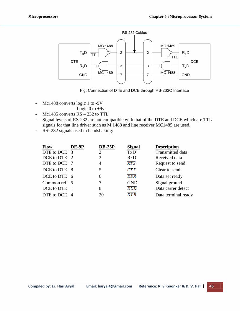
RS -232
- Serial transmission of data is used as an efficient means for transmitting digital
information across long distances, the existing communication lines usually the telephone
lines can be used to transfer information which saves a lot of hardware.
- RS-232C is an interface developed to standardize the interface between data terminal
equipment (DTE) and data communication equipment (DCE) employing serial binary
data exchange. Modem and other devices used to send serial data are called data
communication equipment (DCE). The computers or terminals that are sending or
receiving the data are called data terminal.
- Equipment (DTE) RS- 232C is the interface standard developed by electronic industries
Association (EIA) in response to the need for the signal and handshake standards
between the DTE and DCE.
- It uses 25 pins (DB – 25P) or 9 Pins (DE – 9P) standard where 9 pin standard does not
use all signals i. e. data, control, timing and ground.
- It describes the voltage levels, impendence levels, rise and fall times, maximum bit rate
and maximum capacitance for all signal lines.
- It also specifies that DTE connector should be male and DCE connector should be
female.
- It can send 20kBd for a distance of 50 ft.
- The voltage level for RS-232 are:
o A logic high or 1 , 3V to -15V
o A logic low or 0, +3v to +15v
Normally ±12V voltage levels are used
Microprocessors Chapter 4 : Microprocessor System
Compiled by: Er. Hari Aryal Email: [email protected] Reference: R. S. Gaonkar & D, V. Hall | 45
- Mc1488 converts logic 1 to -9V
Logic 0 to +9v
- Mc1485 converts RS – 232 to TTL
- Signal levels of RS-232 are not compatible with that of the DTE and DCE which are TTL
signals for that line driver such as M 1488 and line receiver MC1485 are used.
- RS- 232 signals used in handshaking:
Flow DE-9P DB-25P Signal Description DTE to DCE 3 2 TxD Transmitted data
DCE to DTE 2 3 RxD Received data
DTE to DCE 7 4 Request to send
DCE to DTE 8 5 Clear to send
DCE to DTE 6 6 Data set ready
Common ref 5 7 GND Signal ground
DCE to DTE 1 8 Data carrer detect
DTE to DCE 4 20 Data terminal ready
Microprocessors Chapter 4 : Microprocessor System
Compiled by: Er. Hari Aryal Email: [email protected] Reference: R. S. Gaonkar & D, V. Hall | 46
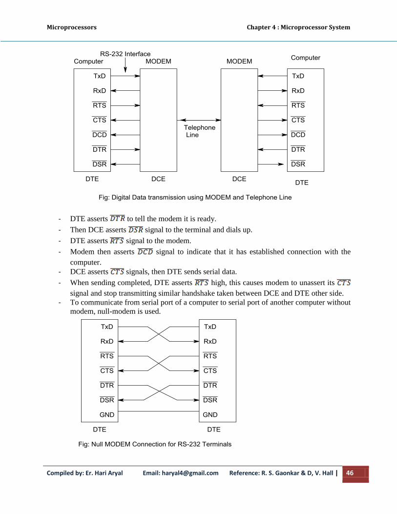
- DTE asserts to tell the modem it is ready.
- Then DCE asserts signal to the terminal and dials up.
- DTE asserts signal to the modem.
- Modem then asserts signal to indicate that it has established connection with the
computer.
- DCE asserts signals, then DTE sends serial data.
- When sending completed, DTE asserts high, this causes modem to unassert its
signal and stop transmitting similar handshake taken between DCE and DTE other side.
- To communicate from serial port of a computer to serial port of another computer without
modem, null-modem is used.
Microprocessors Chapter 4 : Microprocessor System
Compiled by: Er. Hari Aryal Email: [email protected] Reference: R. S. Gaonkar & D, V. Hall | 47
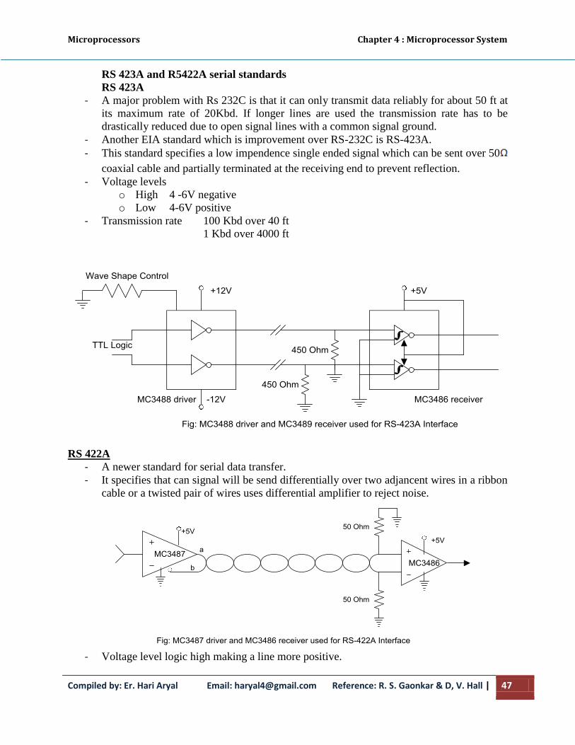
RS 423A and R5422A serial standards
RS 423A
- A major problem with Rs 232C is that it can only transmit data reliably for about 50 ft at
its maximum rate of 20Kbd. If longer lines are used the transmission rate has to be
drastically reduced due to open signal lines with a common signal ground.
- Another EIA standard which is improvement over RS-232C is RS-423A.
- This standard specifies a low impendence single ended signal which can be sent over 50
coaxial cable and partially terminated at the receiving end to prevent reflection.
- Voltage levels
o High 4 -6V negative
o Low 4-6V positive
- Transmission rate 100 Kbd over 40 ft
1 Kbd over 4000 ft
RS 422A
- A newer standard for serial data transfer.
- It specifies that can signal will be send differentially over two adjancent wires in a ribbon
cable or a twisted pair of wires uses differential amplifier to reject noise.
- Voltage level logic high making a line more positive.
Microprocessors Chapter 4 : Microprocessor System
Compiled by: Er. Hari Aryal Email: [email protected] Reference: R. S. Gaonkar & D, V. Hall | 48
- Logic low making a line lines must.
- The voltage difference between the two lines must be greater than 0.4V but less than
12V.
- The mc3487 driver provides a differential voltage of about 2V.
- The center or common mode voltage on the lines must be between -7v and +7v
- Transmission rate is 10000 KBd for 40 FT
- 100 KBD for 4000 ft.
- The high data transfer is because of differential lline functions as a fully terminated
transmission line.
- Mc 3486 receiver only responds to the differential voltage eliminating noise.
Introduction to Direct Memory Access (DMA) & DMA Controllers
During any given bus cycle, one of the system components connected to the system bus is given
control of the bus. This component is said to be the master during that cycle and the component
it is communicating with is said to be the slave. The CPU with its bus control logic is normally
the master, but other specially designed components can gain control of the bus by sending a bus
request to the CPU. After the current bus cycle is completed the CPU will return a bus grant
signal and the component sending the request will become the master.
Taking control of the bus for a bus cycle is called cycle stealing. Just like the bus control logic, a
master must be capable of placing addresses on the address bus and directing the bus activity
during a bus cycle. The components capable of becoming masters are processors (and their bus
control logic) and DMA controllers. Sometimes a DMA controller is associated with a single
interface, but they are often designed to accommodate more than one interface.
This is a process where data is transferred between two peripherals directly without the
involvement of the microprocessor. This process employs the HOLD pin on the microprocessor.
The external DMA controller sends a signal on the HOLD pin to the microprocessor. The
microprocessor completes the current operation and sends a signal on HLDA and stops using the
buses. Once the DMA controller is done, it turns off the HOLD signal and the microprocessor
takes back control of the buses.
Basic DMA operation
The direct memory access (DMA) technique provides direct access to the memory while
the microprocessor is temporarily disabled.
A DMA controller temporarily borrows the address bus, data bus, and control bus from
the microprocessor and transfers the data bytes directly between an I/O port and a series
of memory locations.
The DMA transfer is also used to do high-speed memory-to memory transfers.
Two control signals are used to request and acknowledge a DMA transfer in the
microprocessor-based system.
The HOLD signal is a bus request signal which asks the microprocessor to release control
of the buses after the current bus cycle.
Microprocessors Chapter 4 : Microprocessor System
Compiled by: Er. Hari Aryal Email: [email protected] Reference: R. S. Gaonkar & D, V. Hall | 49
The HLDA signal is a bus grant signal which indicates that the microprocessor has
indeed released control of its buses by placing the buses at their high-impedance states.
The HOLD input has a higher priority than the INTR or NMI interrupt inputs.
DMA Data Transfer scheme
Data transfer from I/O device to memory or vice-versa is controlled by a DMA
controller.
This scheme is employed when large amount of data is to be transferred.
The DMA requests the control of buses through the HOLD signal and the MPU
acknowledges the request through HLDA signal and releases the control of buses to
DMA.
It’s a faster scheme and hence used for high speed printers.
Block (Burst) mode of data transfer
In this scheme the I/O device withdraws the DMA request only after all the data bytes have been
transferred.
Cycle stealing technique
In this scheme the bytes are divided into several parts and after transferring every part the control
of buses is given back to MPU and later stolen back when MPU does not need it.
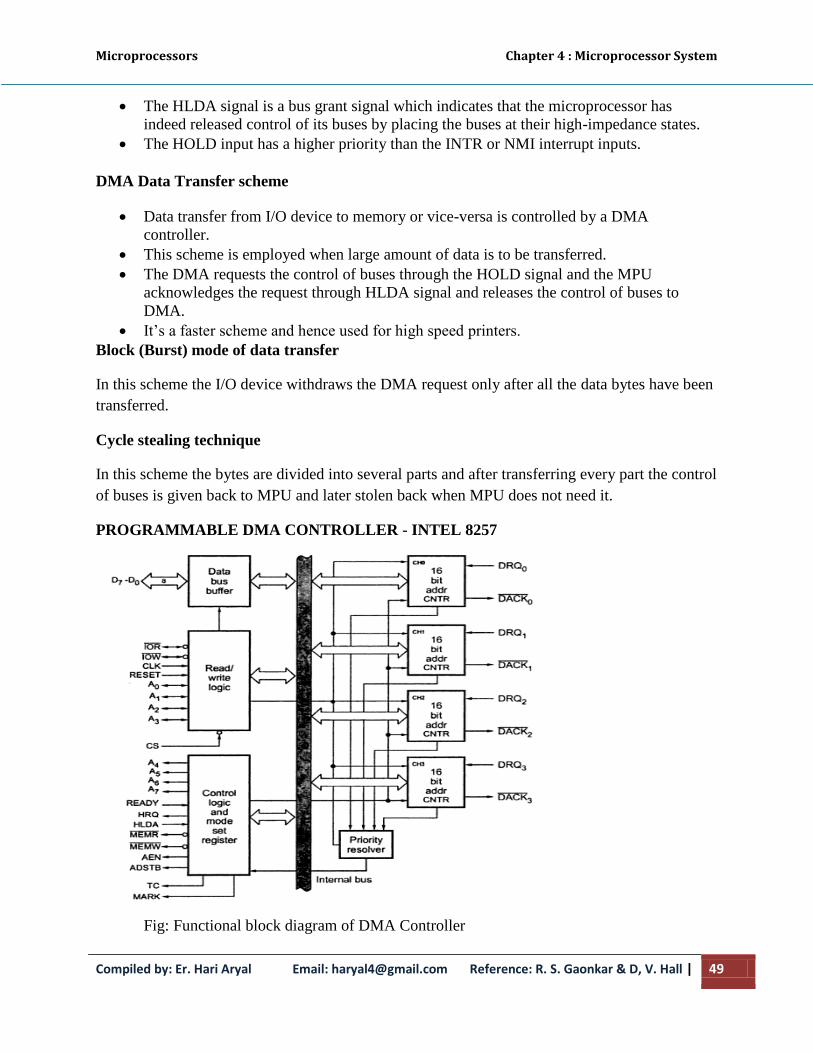
PROGRAMMABLE DMA CONTROLLER - INTEL 8257
Fig: Functional block diagram of DMA Controller

Microprocessors Chapter 4 : Microprocessor System
Compiled by: Er. Hari Aryal Email: [email protected] Reference: R. S. Gaonkar & D, V. Hall | 50
It is a device to transfer the data directly between IO device and memory without through the
CPU. So it performs a high-speed data transfer between memory and I/O device.
The features of 8257 is,
The 8257 has four channels and so it can be used to provide DMA to four I/O devices.
Each channel can be independently programmable to transfer up to 64kb of data by
DMA.
Each channel can be independently perform read transfer, write transfer and verify
transfer.
The functional blocks of 8257 as shown in the above figure are data bus buffer, read/write logic,
control logic, priority resolver and four numbers of DMA channels.
Operation of 8257 DMA Controller
Each channel of 8257 has two programmable 16-bit registers named as address register
and count register.
Address register is used to store the starting address of memory location for DMA data
transfer.
The address in the address register is automatically incremented after every
read/write/verify transfer.
The count register is used to count the number of byte or word transferred by DMA.
In read transfer the data is transferred from memory to I/O device.
In write transfer the data is transferred from I/O device to memory.
Verification operations generate the DMA addresses without generating the DMA
memory and I/O control signals.
The 8257 has two eight bit registers called mode set register and status register.