oceanographic instrument simulator - mbari instrument simulator a.y. chen, b. benson, m. mitchell,...
TRANSCRIPT
Oceanographic Instrument Simulator A.Y. Chen, B. Benson, M. Mitchell, R. Bae,V. Prodanov
Electrical and Computer Engineering Department California Polytechnic State University
San Luis Obispo, CA. 93410 [email protected]
C. D. Kecy Monterey Bay Aquarium Research Institute
7700 Sandholdt Road Moss Landing, CA. 95039
Abstract—The Monterey Bay Aquarium Research Institute (MBARI) established the Free Ocean Carbon Enrichment (FOCE) experiment to study the long term effects of decreased ocean pH levels by developing in-situ platforms [1]. Deep FOCE (dpFOCE) was the first platform, which was deployed in 890 meters of water in Monterey Bay. After the conclusion of dpFOCE, MBARI developed an open source shallow water FOCE (swFOCE) platform to facilitate worldwide shallow water experiments on FOCE [1][2]. A shallow water platform can be more ubiquitous than a deep-water platform as shallow water instruments are less expensive (as it does not have to be designed to withstand the pressure at deep ocean depths) and more easily deployed (they can be deployed right along the coast).
The swFOCE experiment is an open source platform, and MBARI has made the plans available online to anyone interested in studying shallow water carbon enrichment. The Oceanographic instrument simulator (OIS), described in this paper provides the means for MBARI engineers to test the swFOCE platform without attaching the numerous and expensive oceanographic instruments. The Oceanographic Instrument Simulator simulates the various scientific instruments that could be deployed in an actual experiment.
Keywords—oceanographic; engineering; sensor; MBARI; open source; simulator
I. INTRODUCTION As atmospheric CO2 is rising, so is carbon sequestration
in the ocean. The increase in CO2 in our world’s oceans will change its biological composition. In order to better monitor the effect of rising atmospheric CO2 in the ocean, scientists and engineers at the Monterey Bay Aquarium Research Institute (MBARI) have been monitoring the ocean through the Free Ocean Carbon Enrichment (FOCE) experiment. Their first platform, Deep FOCE (dpFOCE) was deployed at 890 meters in Monterey Bay for 17 months from May 2011 to October 2012[1]. After the dpFOCE, shallow-water FOCE (swFOCE) was established as an open source platform to facilitate worldwide shallow water experiments on FOCE. A shallow water platform can be more ubiquitous than a deep-water platform as shallow water instruments are less expensive and more easily deployed.
When an open source platform is made available, it is also useful to make available an inexpensive means to test the platform to insure its operability and functionality. The Oceanographic Instrument Simulator (OIS), the topic of this paper, was designed to give test engineers the ability to test
the functionality of swFOCE without the need for having the actual expensive oceanographic instruments connected to the system. The OIS simulates up to four oceanographic instruments by providing an equivalent electrical load and data stream as the real instrument. Thus, scientists and engineers can connect the OIS to the swFOCE, configure the OIS to simulate the oceanographic instruments they plan to deploy, and test the system to ensure 1. that the power limits of the system are not exceeded and 2. that the data from the ‘sensor’ accurately flows through the various modules of the system.
The rest of this paper is organized as follows: In section 2, we present the block diagram of the swFOCE platform and describe its purpose. In section 3, we describe the hardware and software design of oceanographic instrument simulator (OIS). In section 4, we describe the different tests we preformed to illustrate proper functionality of the OIS including electronic load oscillation testing, thermal testing and parallel testing. We present the power budget in section 5 and conclude in section 6.
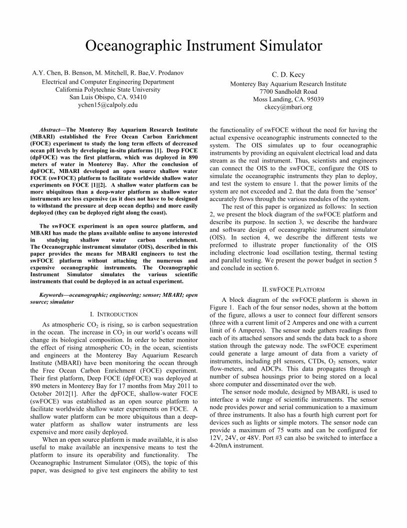
II. SWFOCE PLATFORM A block diagram of the swFOCE platform is shown in
Figure 1. Each of the four sensor nodes, shown at the bottom of the figure, allows a user to connect four different sensors (three with a current limit of 2 Amperes and one with a current limit of 6 Amperes). The sensor node gathers readings from each of its attached sensors and sends the data back to a shore station through the gateway node. The swFOCE experiment could generate a large amount of data from a variety of instruments, including pH sensors, CTDs, O2 sensors, water flow-meters, and ADCPs. This data propagates through a number of subsea housings prior to being stored on a local shore computer and disseminated over the web.
The sensor node module, designed by MBARI, is used to interface a wide range of scientific instruments. The sensor node provides power and serial communication to a maximum of three instruments. It also has a fourth high current port for devices such as lights or simple motors. The sensor node can provide a maximum of 75 watts and can be configured for 12V, 24V, or 48V. Port #3 can also be switched to interface a 4-20mA instrument.
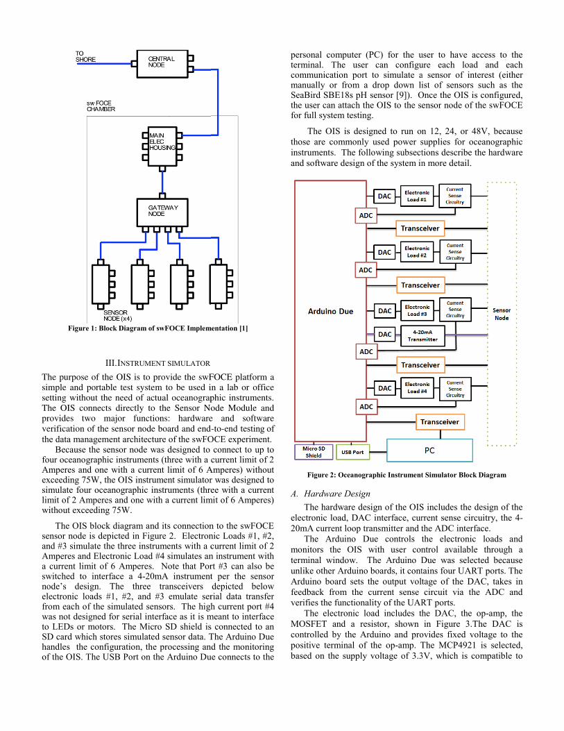
Figure 1: Block Diagram of swFOCE Implem
III. INSTRUMENT SIMULATOR The purpose of the OIS is to provide the swFsimple and portable test system to be used isetting without the need of actual oceanograpThe OIS connects directly to the Sensor Noprovides two major functions: hardwareverification of the sensor node board and endthe data management architecture of the swFO
Because the sensor node was designed to four oceanographic instruments (three with a cAmperes and one with a current limit of 6 Aexceeding 75W, the OIS instrument simulatorsimulate four oceanographic instruments (threlimit of 2 Amperes and one with a current limwithout exceeding 75W.
The OIS block diagram and its connectionsensor node is depicted in Figure 2. Electronand #3 simulate the three instruments with a cAmperes and Electronic Load #4 simulates ana current limit of 6 Amperes. Note that Porswitched to interface a 4-20mA instrumentnode’s design. The three transceivers electronic loads #1, #2, and #3 emulate serfrom each of the simulated sensors. The highwas not designed for serial interface as it is mto LEDs or motors. The Micro SD shield isSD card which stores simulated sensor data. Thandles the configuration, the processing anof the OIS. The USB Port on the Arduino Du
mentation [1]
FOCE platform a in a lab or office phic instruments. ode Module and e and software -to-end testing of
OCE experiment. connect to up to
current limit of 2 Amperes) without r was designed to ee with a current
mit of 6 Amperes)
n to the swFOCE nic Loads #1, #2, current limit of 2 n instrument with rt #3 can also be t per the sensor depicted below rial data transfer h current port #4
meant to interface s connected to an The Arduino Due nd the monitoring ue connects to the
personal computer (PC) for the uterminal. The user can configucommunication port to simulate amanually or from a drop down liSeaBird SBE18s pH sensor [9]). Othe user can attach the OIS to the sefor full system testing.
The OIS is designed to run onthose are commonly used power sinstruments. The following subsectand software design of the system in
Figure 2: Oceanographic Instrument
A. Hardware Design The hardware design of the OIS
electronic load, DAC interface, cur20mA current loop transmitter and t
The Arduino Due controls tmonitors the OIS with user conterminal window. The Arduino Dunlike other Arduino boards, it contArduino board sets the output voltfeedback from the current sense verifies the functionality of the UAR
The electronic load includes thMOSFET and a resistor, shown controlled by the Arduino and propositive terminal of the op-amp. Tbased on the supply voltage of 3.3
user to have access to the ure each load and each a sensor of interest (either ist of sensors such as the
Once the OIS is configured, ensor node of the swFOCE
n 12, 24, or 48V, because supplies for oceanographic tions describe the hardware n more detail.
t Simulator Block Diagram
S includes the design of the rrent sense circuitry, the 4-the ADC interface. the electronic loads and ntrol available through a Due was selected because tains four UART ports. The tage of the DAC, takes in circuit via the ADC and
RT ports. he DAC, the op-amp, the in Figure 3.The DAC is
ovides fixed voltage to the The MCP4921 is selected, 3V, which is compatible to

the output voltage from the Arduino Due. The DAC controlled programmable current sink circuit is shown in Figure 3. The op-amp creates a negative feedback loop from the gate of the MOSFET via the resistor then back to the negative terminal of the op-amp. Depending upon the input voltage from the DAC, the current conducted by the MOSFET and resistor varies. The output voltage from the Arduino goes up to 3.3V; therefore the range of the DAC output is set to vary from 0V to 3V. To sink in 0A to 2A, a resistor with value 1.5Ω is selected. The op-amp and the 1.5Ω sense resistor form an integral control that forces the MOSFET’s current to be exactly Vin/1.5Ω. This value assumes stable loop and op-amp with zero offset. LM358 was chosen for its ground-sensing capabilities [3] and the MOSFET FDP050AN06A0 for its large current and power dissipation capabilities [4].
Figure 3: DAC Controlled Electronic Load Schematic
The current sense circuit, as shown in Figure 4, is used to monitor the output current and shut down the circuit should the current exceed 75W. The LT1999 is selected due to simplicity. To increase the resolution of the current sense circuit, the offset of the VREF is set at 1V. The current sense circuit can sense voltages ranging from 1-3Vdue to the offset of the VREF. The LT1999 chip has an offset of 2.5V at VREF, shown in Figure 5. In order to lower the VREF, an additional 52.3k resistor is added to lower the VREF to 1V. Due to the range of the ADC on the Arduino Due, we were able to sense voltages from 1V to 3V.
Figure 4: Circuit Sense Circuit Schematic
Figure 5: LT1999 Block Diagram [8]
A single 4-20mA current loop transmitter is designed for OIS at load #3 to communicate with 4-20mA instruments on the Sensor Node. The 4-20ma current loop transmitter, XTR117 [7], shown in Figure 6, from Texas Instrument is selected due to the simplicity of the design. According to the datasheet, the chip is built around Eq. (1). Since the output of the DAC was originally range from 0V to 3V, Eq. (1) is used to calculate the resistance of 15k.
(1)
Figure 6: 4-20mA Transmitter Loop Schematic [7]
B. Software Design The software for the OIS is a terminal based program that
allows the user to configure and run the simulator. The main menu screen for the terminal program is shown in Figure 7. Option 1 allows the user to specify the sensor node’s DC-DC converter’s voltage (12, 24, or 48V). Option 2 allows the user to configure each port with a desired electronic load and data stream to simulate the desired sensor and Option 3 allows the user to check any ports that have already been configured. Option 4 can test each individual port’s electronic load and Option 5 can test each port’s serial communication. Option 6 can run or stop individual ports. Option 7 is currently used for
testing individual commands to simulate tsensor. In the future, these commands will into Option 5 for testing the serial communica
Figure 7: Main Menu Screen Figure 8 shows the software design in mo
illustrating the sub menus/selections that appemain menu option is pressed.
Figure 8: Software System Diagram
When all ports have been configured andthe OIS is connected to the sensor node, the Oto any serial commands sent from the sensosoftware program streams simulated data acurrent consumption on all active ports to enexceed the system's maximum power, 75W. an example of the OIS responding to thecommand of “gethd" directed toward the SBThe OIS interprets the command and responappropriate information (in this case, hinformation) which is stored on the OIS’ SD c
Figure 9: Data Format for pH Sensor
the SBE18s pH be incorporated
ation.
ore detail -ear after each
[2]
d are running and OIS will respond r node. The OIS
and monitors the nsure they do not
Figure 9 shows e sensor node’s
BE18s pH sensor. ds back with the
hardware device card.
r [2]
IV. TEST
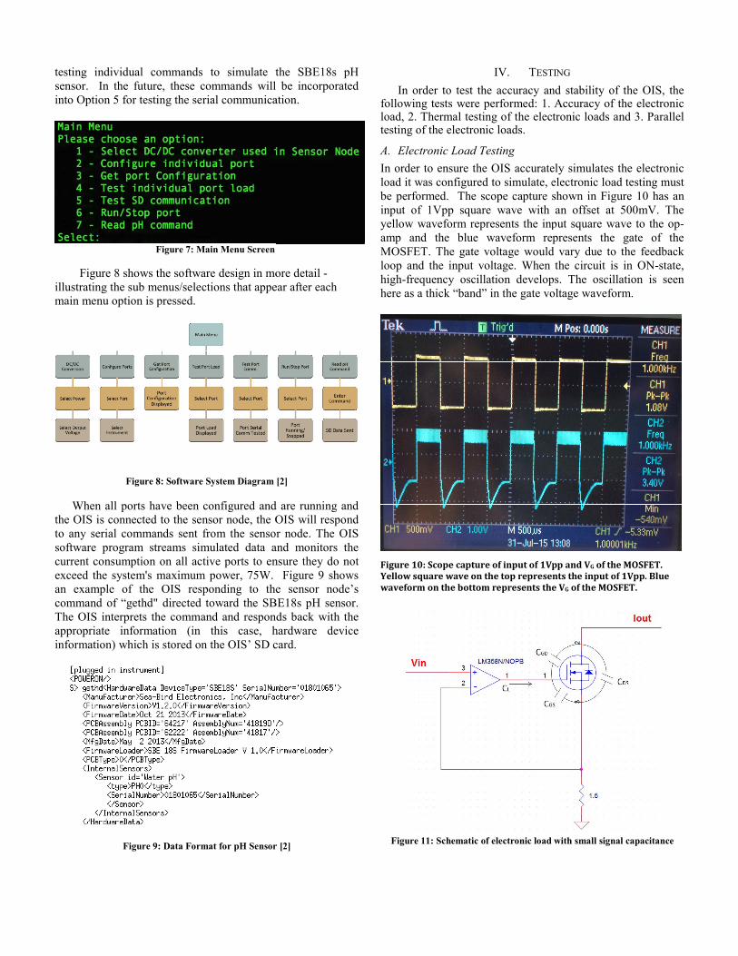
In order to test the accuracy anfollowing tests were performed: 1. load, 2. Thermal testing of the electesting of the electronic loads. A. Electronic Load Testing In order to ensure the OIS accurateload it was configured to simulate, ebe performed. The scope capture input of 1Vpp square wave with yellow waveform represents the inpamp and the blue waveform reMOSFET. The gate voltage wouldloop and the input voltage. When high-frequency oscillation develophere as a thick “band” in the gate vo
Figure 10: Scope capture of input of 1VpYellow square wave on the top represewaveform on the bottom represents the
Figure 11: Schematic of electronic load
TING nd stability of the OIS, the Accuracy of the electronic tronic loads and 3. Parallel
ely simulates the electronic electronic load testing must shown in Figure 10 has an an offset at 500mV. The
put square wave to the op-presents the gate of the
d vary due to the feedback the circuit is in ON-state,
ps. The oscillation is seen oltage waveform.
pp and VG of the MOSFET. nts the input of 1Vpp. Blue e VG of the MOSFET.
with small signal capacitance
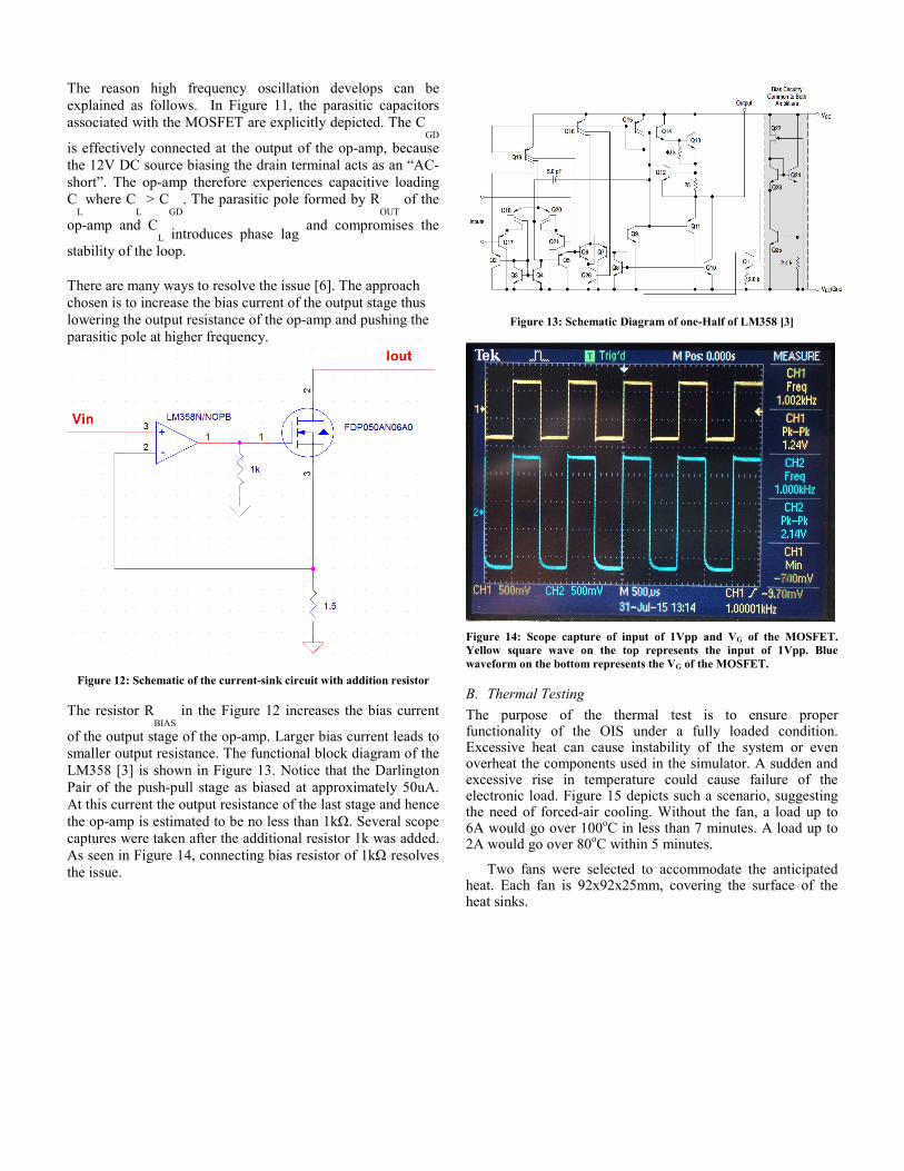
The reason high frequency oscillation develops can be explained as follows. In Figure 11, the parasitic capacitors associated with the MOSFET are explicitly depicted. The C
GD is effectively connected at the output of the op-amp, because the 12V DC source biasing the drain terminal acts as an “AC-short”. The op-amp therefore experiences capacitive loading C
L where C
L > CGD
. The parasitic pole formed by ROUT of the
op-amp and CL introduces phase lag and compromises the
stability of the loop.
There are many ways to resolve the issue [6]. The approach chosen is to increase the bias current of the output stage thus lowering the output resistance of the op-amp and pushing the parasitic pole at higher frequency.
Figure 12: Schematic of the current-sink circuit with addition resistor
The resistor RBIAS
in the Figure 12 increases the bias current
of the output stage of the op-amp. Larger bias current leads to smaller output resistance. The functional block diagram of the LM358 [3] is shown in Figure 13. Notice that the Darlington Pair of the push-pull stage as biased at approximately 50uA. At this current the output resistance of the last stage and hence the op-amp is estimated to be no less than 1kΩ. Several scope captures were taken after the additional resistor 1k was added. As seen in Figure 14, connecting bias resistor of 1kΩ resolves the issue.
Figure 13: Schematic Diagram of one-Half of LM358 [3]
Figure 14: Scope capture of input of 1Vpp and VG of the MOSFET. Yellow square wave on the top represents the input of 1Vpp. Blue waveform on the bottom represents the VG of the MOSFET.
B. Thermal Testing The purpose of the thermal test is to ensure proper functionality of the OIS under a fully loaded condition. Excessive heat can cause instability of the system or even overheat the components used in the simulator. A sudden and excessive rise in temperature could cause failure of the electronic load. Figure 15 depicts such a scenario, suggesting the need of forced-air cooling. Without the fan, a load up to 6A would go over 100oC in less than 7 minutes. A load up to 2A would go over 80oC within 5 minutes.
Two fans were selected to accommodate the anticipated heat. Each fan is 92x92x25mm, covering the surface of the heat sinks.

Figure 15: Thermal Test without Fa
With the fan on, as shown in Figure 16, would remain around 45oC over a long periodthe necessary stability of the entire system.
Figure 16: Thermal Test with Fan
C. Parallel Testing The purpose of the OIS is to sim
oceanographic sensors simultaneously, thus pmultiple sensors is necessary to insure the system. As shown in Figure 17, Figure 18, anparallel testing result demonstrates the accurThe expected current is the current the user wOIS and the output current is the current thathe power supply. To ensure the system does power rating, three loads of 2A and the sintested separately. Figure 17, Figure 18 and that the overall OIS system remains linear anall loads are running.
an
a load up to 6A d, thus providing
n
mulate multiple parallel testing of
accuracy of the nd Figure 19, the racy of the OIS.
would input to the at is displayed on
not exceed 75W ngle 6A load are
Figure 19 show nd accurate when
Figure 17: Single l
Figure 18: Parallel testing for thre
Figure 19: Parallel testin
V. POWER BU
The following is the estimated powOIS will be supplied with 3.3V andand supplied with 12V from an(Hewlett Packard 6028A DC Pow200W). The estimated powerexperimental power supply, showshown in Figure 12 would increasethe op-amps.
load test
ee loads at the same time
ng for Load #4
DGET wer budget for the OIS. The d 5V from the Arduino Due n external power supply wer Supply 0-60V/0-10A, r budget matched the
wn in Table 1. The RBIAS the power consumption of
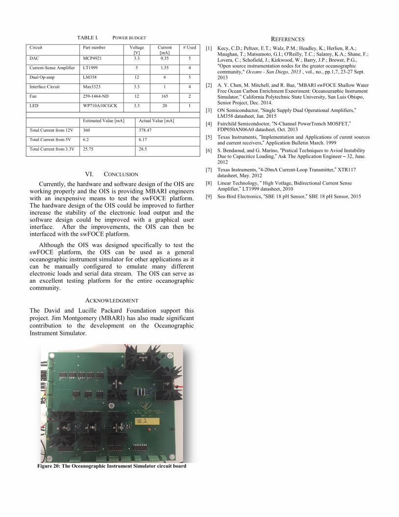
TABLE I. POWER BUDGET
Circuit Part number Voltage [V]
DAC MCP4921 3.3
Current-Sense Amplifier LT1999 5
Dual Op-amp LM358 12
Interface Circuit Max3323 3.3
Fan 259-1464-ND 12
LED WP710A10CGCK 3.3
Estimated Value [mA] Actua
Total Current from 12V 360 378.4
Total Current from 5V 6.2 6.17
Total Current from 3.3V 25.75 28.5
VI. CONCLUSION Currently, the hardware and software desig
working properly and the OIS is providing Mwith an inexpensive means to test the swThe hardware design of the OIS could be impincrease the stability of the electronic loadsoftware design could be improved with ainterface. After the improvements, the Ointerfaced with the swFOCE platform.
Although the OIS was designed specifiswFOCE platform, the OIS can be usedoceanographic instrument simulator for other can be manually configured to emulate electronic loads and serial data stream. The Oan excellent testing platform for the entircommunity.
ACKNOWLEDGMENT The David and Lucille Packard Foundatiproject. Jim Montgomery (MBARI) has also contribution to the development on the Instrument Simulator.
Figure 20: The Oceanographic Instrument Simulat
Current [mA]
# Used
0.35 5
1.55 4
6 5
1 4
165 2
20 1
al Value [mA]
7
gn of the OIS are MBARI engineers wFOCE platform.
proved to further d output and the a graphical user
OIS can then be
cally to test the d as a general applications as it many different
OIS can serve as e oceanographic
ion support this made significant
Oceanographic
tor circuit board
REFERENC
[1] Kecy, C.D.; Peltzer, E.T.; Walz, P.M.; Maughan, T.; Matsumoto, G.I.; O'ReillLovera, C.; Schofield, J.; Kirkwood, W"Open source instrumentation nodes focommunity," Oceans - San Diego, 2012013
[2] A. Y. Chen, M. Mitchell, and R. Bae, “Free Ocean Carbon Enrichment ExperiSimulator,” California Polytechnic StatSenior Project, Dec. 2014.
[3] ON Semiconductor, “Single Supply DuLM358 datasheet, Jan. 2015
[4] Fairchild Semicondoctor, “N-Channel PFDP050AN06A0 datasheet, Oct. 2013
[5] Texas Instruments, “Implementation anand current receivers,” Application Bul
[6] S. Bendaoud, and G. Marino, “Pratical Due to Capacitice Loading,” Ask The A2012
[7] Texas Instruments, “4-20mA Current-Ldatasheet, May. 2012
[8] Linear Technology, “ High Votlage, BiAmplifier,” LT1999 datasheet, 2010
[9] Sea-Bird Electronics, “SBE 18 pH Sens
ES Headley, K.; Herlien, R.A.;
ly, T.C.; Salamy, K.A.; Shane, F.; W.; Barry, J.P.; Brewer, P.G., or the greater oceanographic 3 , vol., no., pp.1,7, 23-27 Sept.
MBARI swFOCE Shallow Water iment: Oceanographic Instrument te University, San Luis Obispo,
ual Operational Amplifiers,”
PowerTrench MOSFET,”
nd Applications of curent sources lletin March. 1999 Techniques to Aviod Instability
Application Engineer – 32, June.
Loop Transmitter,” XTR117
directional Current Sense
sor,” SBE 18 pH Sensor, 2015