old company name in catalogs and other documents sheets/renesas/cmos-9hd_famil… · old company...
TRANSCRIPT
To our customers,
Old Company Name in Catalogs and Other Documents
On April 1st, 2010, NEC Electronics Corporation merged with Renesas Technology
Corporation, and Renesas Electronics Corporation took over all the business of both companies. Therefore, although the old company name remains in this document, it is a valid Renesas Electronics document. We appreciate your understanding.
Renesas Electronics website: http://www.renesas.com
April 1st, 2010 Renesas Electronics Corporation
Issued by: Renesas Electronics Corporation (http://www.renesas.com)
Send any inquiries to http://www.renesas.com/inquiry.

Notice 1. All information included in this document is current as of the date this document is issued. Such information, however, is
subject to change without any prior notice. Before purchasing or using any Renesas Electronics products listed herein, please confirm the latest product information with a Renesas Electronics sales office. Also, please pay regular and careful attention to additional and different information to be disclosed by Renesas Electronics such as that disclosed through our website.
2. Renesas Electronics does not assume any liability for infringement of patents, copyrights, or other intellectual property rights of third parties by or arising from the use of Renesas Electronics products or technical information described in this document. No license, express, implied or otherwise, is granted hereby under any patents, copyrights or other intellectual property rights of Renesas Electronics or others.
3. You should not alter, modify, copy, or otherwise misappropriate any Renesas Electronics product, whether in whole or in part. 4. Descriptions of circuits, software and other related information in this document are provided only to illustrate the operation of
semiconductor products and application examples. You are fully responsible for the incorporation of these circuits, software, and information in the design of your equipment. Renesas Electronics assumes no responsibility for any losses incurred by you or third parties arising from the use of these circuits, software, or information.
5. When exporting the products or technology described in this document, you should comply with the applicable export control laws and regulations and follow the procedures required by such laws and regulations. You should not use Renesas Electronics products or the technology described in this document for any purpose relating to military applications or use by the military, including but not limited to the development of weapons of mass destruction. Renesas Electronics products and technology may not be used for or incorporated into any products or systems whose manufacture, use, or sale is prohibited under any applicable domestic or foreign laws or regulations.
6. Renesas Electronics has used reasonable care in preparing the information included in this document, but Renesas Electronics does not warrant that such information is error free. Renesas Electronics assumes no liability whatsoever for any damages incurred by you resulting from errors in or omissions from the information included herein.
7. Renesas Electronics products are classified according to the following three quality grades: “Standard”, “High Quality”, and “Specific”. The recommended applications for each Renesas Electronics product depends on the product’s quality grade, as indicated below. You must check the quality grade of each Renesas Electronics product before using it in a particular application. You may not use any Renesas Electronics product for any application categorized as “Specific” without the prior written consent of Renesas Electronics. Further, you may not use any Renesas Electronics product for any application for which it is not intended without the prior written consent of Renesas Electronics. Renesas Electronics shall not be in any way liable for any damages or losses incurred by you or third parties arising from the use of any Renesas Electronics product for an application categorized as “Specific” or for which the product is not intended where you have failed to obtain the prior written consent of Renesas Electronics. The quality grade of each Renesas Electronics product is “Standard” unless otherwise expressly specified in a Renesas Electronics data sheets or data books, etc.
“Standard”: Computers; office equipment; communications equipment; test and measurement equipment; audio and visual equipment; home electronic appliances; machine tools; personal electronic equipment; and industrial robots.
“High Quality”: Transportation equipment (automobiles, trains, ships, etc.); traffic control systems; anti-disaster systems; anti-crime systems; safety equipment; and medical equipment not specifically designed for life support.
“Specific”: Aircraft; aerospace equipment; submersible repeaters; nuclear reactor control systems; medical equipment or systems for life support (e.g. artificial life support devices or systems), surgical implantations, or healthcare intervention (e.g. excision, etc.), and any other applications or purposes that pose a direct threat to human life.
8. You should use the Renesas Electronics products described in this document within the range specified by Renesas Electronics, especially with respect to the maximum rating, operating supply voltage range, movement power voltage range, heat radiation characteristics, installation and other product characteristics. Renesas Electronics shall have no liability for malfunctions or damages arising out of the use of Renesas Electronics products beyond such specified ranges.
9. Although Renesas Electronics endeavors to improve the quality and reliability of its products, semiconductor products have specific characteristics such as the occurrence of failure at a certain rate and malfunctions under certain use conditions. Further, Renesas Electronics products are not subject to radiation resistance design. Please be sure to implement safety measures to guard them against the possibility of physical injury, and injury or damage caused by fire in the event of the failure of a Renesas Electronics product, such as safety design for hardware and software including but not limited to redundancy, fire control and malfunction prevention, appropriate treatment for aging degradation or any other appropriate measures. Because the evaluation of microcomputer software alone is very difficult, please evaluate the safety of the final products or system manufactured by you.
10. Please contact a Renesas Electronics sales office for details as to environmental matters such as the environmental compatibility of each Renesas Electronics product. Please use Renesas Electronics products in compliance with all applicable laws and regulations that regulate the inclusion or use of controlled substances, including without limitation, the EU RoHS Directive. Renesas Electronics assumes no liability for damages or losses occurring as a result of your noncompliance with applicable laws and regulations.
11. This document may not be reproduced or duplicated, in any form, in whole or in part, without prior written consent of Renesas Electronics.
12. Please contact a Renesas Electronics sales office if you have any questions regarding the information contained in this document or Renesas Electronics products, or if you have any other inquiries.
(Note 1) “Renesas Electronics” as used in this document means Renesas Electronics Corporation and also includes its majority-owned subsidiaries.
(Note 2) “Renesas Electronics product(s)” means any product developed or manufactured by or for Renesas Electronics.
Second-generation highly integrated 0.35 µm CMOS gate array
Considerable cost reduction
Second-generation highly integra
Considerable cost reduction
CMOS-9HD Family0.35 µm CMOS Gate Array
NewProducts

2 Pamphlet A12852EJ3V0PF00
CMOS-9
1.0
0.4
CMOS-9HD
CMOS-8L CMOS-9HD
53k gates
30k gates
FEATURES
The CMOS-9HD Family is a channel-less type gate array that uses the 0.35-µm leading-edge process and realizes 960,000
usable gates. This family is adaptable for both high-speed and low-power consumption systems. Currently supporting a
3.3-V supply voltage, it is expected that the future lineup will be able to support a supply voltage of 2.5 V.
High Integration/Low Power Consumption• Maximum of 960,000 usable gates integrated
• Improved cell structure, higher density
• Lower power consumption (a further 30% reduction from CMOS-9)
In Pursuit of Lower Cost• Enhanced cost competitiveness through chip-size shrinkage
• Fewer gate masters leading to further cost reduction
(Example) Comparison with CMOS-8L
Although the 30k-gate CMOS-8L and the 53k-gate CMOS-9HD are similar in terms of price, because the
cell density is higher in the CMOS-9HD, for an area of 30k integrated gates or more, the CMOS-9HD is
the more cost-competitive choice.
Note that the applicable-package pin-count range differs depending on the chip size, even if the gate
scale is identical.
Cell size comparison (1 cell)
CMOS-9: NEC's conventional 0.35-µm gate array
Chip size comparison
CMOS-8L: NEC's conventional 0.5-µm gate array

3Pamphlet A12852EJ3V0PF00
Ultra High-Speed Operation• tPD = 131 ps (2-input NAND, fanout = 1, standard wiring length)
• tPD = 107 ps (2-input NAND (power gate), fanout = 1, standard wiring length)
• tPD = 229 ps (input buffer, fanout = 1, standard wiring length)
• tPD = 222 ps (input buffer, standard load)
• tPD = 1396 ps (output buffer, CL = 50 pF)
Provision of Function Block Enabling High Speed/High Integration• Including high speed and low power, compatible with CMOS-8L Family
• Scan path block
• Driver for clock tree synthesis
• Asynchronous single-port RAM (45 types)
• Asynchronous dual-port RAM (45 types)
• Asynchronous compiled single-port RAM
• Synchronous/asynchronous compiled dual-port RAM
Abundance of Peripheral Blocks• LVTTL/TTL 5-V withstand voltage interface buffer • Low-noise buffer
• LVTTL interface buffer with fail safe function • Buffers with on-chip pull-up resistors (5 kΩ, 50 kΩ)
• High drive capacity buffer (IOL = 24 mA) • Buffers with on-chip pull-down resistors (50 kΩ)
• PCI • Digital PLL (33 to 80 MHz)
• GTL+ • Digital PLL (multiple)
Power Consumption• 0.524 µW/MHz/cell (Internal gates, VDD = 3.3 V)
Support of Variety of Pin Count Packages• 100- to 304-pin plastic QFP (fine-pitch)
• 160-pin, 208-pin plastic QFP (fine-pitch, with heat spreader)
• 48- to 120-pin plastic TQFP
• 144-pin plastic LQFP
• 225- to 352-pin plastic BGA
• 108- to 304-pin plastic FBGA
• 256- to 696-pin tape BGA (with heat spreader)
4 Pamphlet A12852EJ3V0PF00
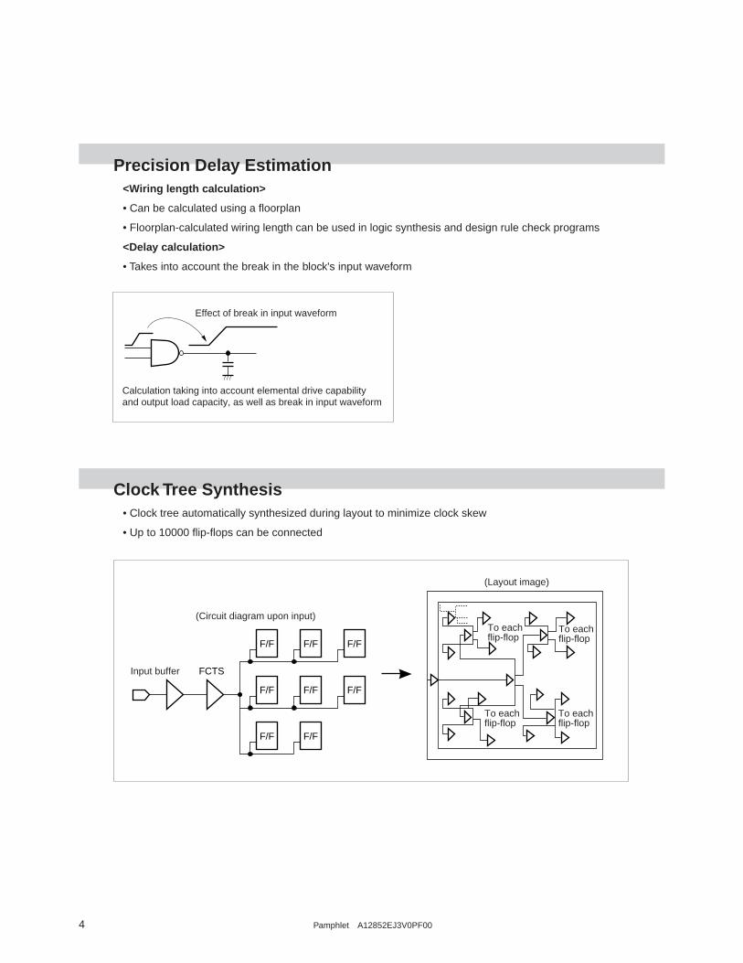
Effect of break in input waveform
Calculation taking into account elemental drive capabilityand output load capacity, as well as break in input waveform
(Circuit diagram upon input)
(Layout image)
Input buffer FCTS
F/F F/F F/F
To eachflip-flop
To eachflip-flop
To eachflip-flop
To eachflip-flop
F/F F/F F/F
F/F F/F
Precision Delay Estimation<Wiring length calculation>
• Can be calculated using a floorplan
• Floorplan-calculated wiring length can be used in logic synthesis and design rule check programs
<Delay calculation>
• Takes into account the break in the block's input waveform
Clock Tree Synthesis• Clock tree automatically synthesized during layout to minimize clock skew
• Up to 10000 flip-flops can be connected

5Pamphlet A12852EJ3V0PF00
Multifarious Function Block Mounting CapabilityThe function blocks ensure functional compatibility with conventional products and facilitate transfer or appropriation
of existing design data.
Note Standard interface recommended by Intel Corp. (PCI = Peripheral Component Interconnect)
Applications (Supported Fields)All fields from large-scale high-speed processing systems to small and medium scale general applications are
covered.
• Multimedia market
PC, AV, moving picture processing, 3D, etc.
• Communications market
High-speed communication, cellular terminals, etc.
• OA, industrial, and other applications.
Memory block
RAMSoft macroCompiled RAM macroROM macro
CPU peripheral block
Serial interface unitParallel interface unitInterrupt controller, etc.
Logic
CounterShift registerFlip-flops, etc.Digital PLL (33 to 80 MHz)Digital PLL (Multiple)
Interface block
GTL+PCINote
5-V withstand voltage/LVTTL bufferLow-noise buffer3-state buffer
Open-drain bufferLVTTL interface buffer with fail safe functionHigh drive capacity buffer (IOL = 24 mA)Buffers with pull-up resistors (5 kΩ, 50 kΩ)Buffers with pull-down resistors (50 kΩ)

6 Pamphlet A12852EJ3V0PF00
PRODUCT OUTLINE
List of Product Types
3-layer wiring
Part Number µPD65943 µPD65944 µPD65945 µPD65946 µPD65948 µPD65949 µPD65951 µPD65954 µPD65956 µPD65958
Number of signals 156 180 200 252 308 364 416 496 572 692
Number of pads 172 196 216 268 324 380 436 516 588 708
Number of integrated gates 75740 100602 128338 202630 312684 437136 585390 835664 1096452 1615646
Number of usable gates 53018 70421 89836 141841 218879 262281 321964 459615 603048 807823
Remark The actual number of usable signal lines depends on the package and the number of power supply and GND pins used.
4-layer wiring
Part Number µPD65961 µPD65964 µPD65966 µPD65968 µPD65969 µPD65970 µPD65971
Number of signals – – – – – – –
Number of pads 436 516 588 708 764 820 876
Number of integrated gates 585390 835664 1096452 1615646 1904700 2196592 2509284
Number of usable gates 380503 54318 712693 969387 1142820 1317955 1505570
Remark The actual number of usable signal lines depends on the package and the number of power supply and GND pins used.
7Pamphlet A12852EJ3V0PF00
List of Packages
3-layer wiring
Package Pins µPD65943 µPD65944 µPD65945 µPD65946 µPD65948
Plastic QFP (fine-pitch) 100
120 – – – –
144
160
176 –
208 – –
240 – – –
304 – – – –
Plastic QFP (fine-pitch)Note 160 – – – – –
208 – – – – –
Plastic TQFP 48 – – – –
64 – – – –
80 –
100 – – –
120 – –
Plastic LQFP 144 – – – –
Plastic BGA 225 – – –
256 – – – –
272 – – – –
313 – – – – –
352 – – – – –
Plastic FBGA 108
144
160
176 –
208 – – – – –
240 – – – – –
304 – – – – –
Plastic BGA (advanced) 672 – – – – –
Tape BGANote 256 – – –
352 – – – – –
420 – – – – –
500 – – – – –
576 – – – – –
696 – – – – –
Note With heat spreaderRemark : Supported, – : Not supported, Blank : Under consideration
(1/2)
8 Pamphlet A12852EJ3V0PF00
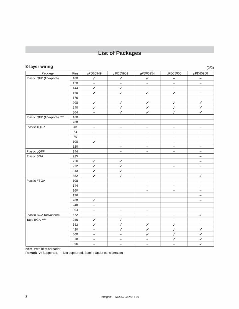
List of Packages
3-layer wiring
Package Pins µPD65949 µPD65951 µPD65954 µPD65956 µPD65958
Plastic QFP (fine-pitch) 100 – –
120 – – – – –
144 – – –
160 –
176 –
208
240
304 –
Plastic QFP (fine-pitch) Note 160
208
Plastic TQFP 48 – – – – –
64 – – – – –
80 – – – – –
100 – – – –
120 – – – –
Plastic LQFP 144 – – – –
Plastic BGA 225 –
256 –
272 – –
313
352
Plastic FBGA 108 – – – – –
144 – – –
160 – – –
176 –
208 –
240 –
304 – – –
Plastic BGA (advanced) 672 – – – –
Tape BGA Note 256 – –
352 –
420 –
500 – –
576 – – –
696 – – – –
Note With heat spreaderRemark : Supported, – : Not supported, Blank : Under consideration
(2/2)

9Pamphlet A12852EJ3V0PF00
List of Packages
4-layer wiring
Package Pins µPD65961 µPD65964 µPD65966 µPD65968 µPD65969
Plastic QFP (fine-pitch)Note 160 – – – – –
208
Tape BGANote 256 – – – – –
352 –
420
500 –
576 – –
696 – –
Plastic BGA (advanced) 672 – – –
Note With heat spreaderRemark – : Not supported, Blank : Under consideration
(1/2)
4-layer wiring
Package Pins µPD65970 µPD65971
Plastic QFP (fine-pitch)Note 160 – –
208
Tape BGANote 256 – –
352
420
500
576
696
Plastic BGA (advanced) 672
Note With heat spreaderRemark – : Not supported, Blank : Under consideration
(2/2)

10 Pamphlet A12852EJ3V0PF00
ELECTRICAL SPECIFICATIONS
Absolute Maximum Ratings
Parameter Symbol Conditions Ratings Unit
Supply voltage VDD –0.5 to +4.6 V
Input voltage
LVTTL interface buffer VI VI < VDD + 0.5 V –0.5 to +4.6 V
LVTTL interface buffer VI VI < VDD + 0.5 V –0.5 to +4.6 V
with fail safe function
TTL 5-V withstand voltage interface buffer VI VI < VDD + 3.0 V –0.5 to +6.6 V
Output voltage
LVTTL output buffer VO VO < VDD + 0.5 V –0.5 to +4.6 V
TTL 5-V output buffer VO VO < VDD + 3.0 V –0.5 to +6.6 V
5-V output buffer for CMOS VO VO < VDD + 3.0 V –0.5 to +6.6 V
Input/output voltage VI/VO Normal I/O pin –0.5 to VDD + 0.5 V
Output currentNote IO IOL = 1 mA (FV0A) 3 mA
IOL = 2 mA (FV0B) 7 mA
IOL = 3 mA (FO09) 10 mA
IOL = 6 mA (FO04) 20 mA
IOL = 9 mA (FO01) 30 mA
IOL = 12 mA (FO02) 40 mA
IOL = 18 mA (FO03) 60 mA
IOL = 24 mA (FO06) 75 mA
Operating ambient temperature TA –40 to +85 °C
Storage temperature Tstg –65 to +150 °CNote Output current: Indicates the maximum value of the current that is allowed to flow directly through this output pin.Remark With the exception of the buffer with fail safe function, be sure to input voltage to the I/O pins only after the supply voltage has
been fixed.
11Pamphlet A12852EJ3V0PF00
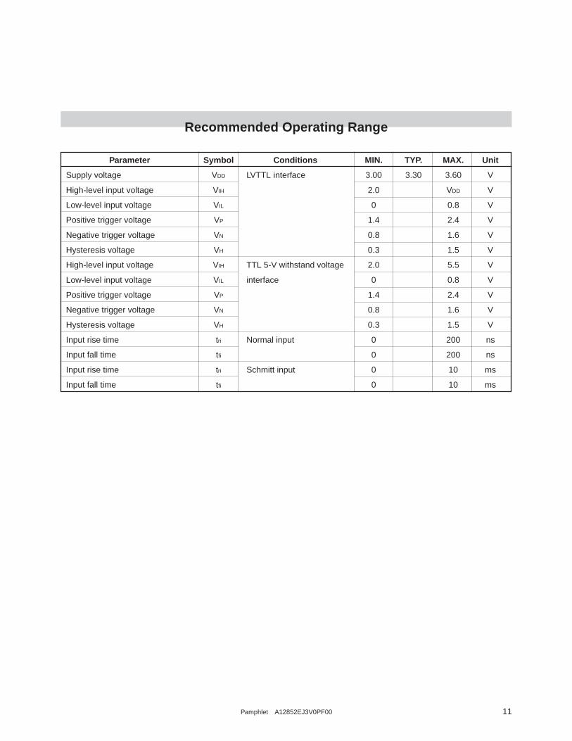
Recommended Operating Range
Parameter Symbol Conditions MIN. TYP. MAX. Unit
Supply voltage VDD LVTTL interface 3.00 3.30 3.60 V
High-level input voltage VIH 2.0 VDD V
Low-level input voltage VIL 0 0.8 V
Positive trigger voltage VP 1.4 2.4 V
Negative trigger voltage VN 0.8 1.6 V
Hysteresis voltage VH 0.3 1.5 V
High-level input voltage VIH TTL 5-V withstand voltage 2.0 5.5 V
Low-level input voltage VIL interface 0 0.8 V
Positive trigger voltage VP 1.4 2.4 V
Negative trigger voltage VN 0.8 1.6 V
Hysteresis voltage VH 0.3 1.5 V
Input rise time tri Normal input 0 200 ns
Input fall time tfi 0 200 ns
Input rise time tri Schmitt input 0 10 ms
Input fall time tfi 0 10 ms

12 Pamphlet A12852EJ3V0PF00
DC Characteristics (V DD = 3.3 V ±0.3 V)(1/3)
Parameter Symbol Conditions MIN. TYP. MAX. Unit
Static current consumptionNote 1
µPD65943, µPD65944, IDDS VI = VDD or GND 2.0 300 µA
µPD65945, µPD65946,
µPD65948, µPD65949,
µPD65951, µPD65954, IDDS VI = VDD or GND 0 400 µA
µPD65956
µPD65958 IDDS VI = VDD or GND 4.0 800 µA
Off-state output currentNote 2
LVTTL output IOZ VO = VDD or GND ±10 µA
TTL 5-V withstand voltage output IOZ VO = VDD or GND ±10 µA
5-V withstand voltage for CMOS IOZ VO = VDD or GND ±10 µA
Output current flowNote 3 IR VPU = 5.5 V, RPU =2 kΩ, 0.1 µA
5-V output for CMOS VO = 3.0 V
Output short-circuit currentNote 4 IOS VO = GND –250 mA
Input leakage current
Normal input II VI = VDD or GND ±1.0 µA
With pull-up resistor (50 kΩ) II VI = GND –28 –83 –190 µA
With pull-up resistor (5 kΩ) II VI = GND –280 –700 –1900 µA
With pull-down resistor (50 kΩ) II VI = VDD 28 83 190 µA
Pull-up resistor 50 kΩ RPU 18.9 39.8 107.1 kΩ
Pull-up resistor 5 kΩ RPU 1.9 4.7 10.7 kΩ
Pull-down resistor 50 kΩ RPD 18.9 39.8 107.1 kΩNotes 1. When using I/O blocks (etc.) with pull-up/pull-down resistors incorporated, the static current consumption increases.
2. Because there is a bias toward the 5-V protection circuit in the TTL 5-V withstand voltage and 5-V withstand voltage for CMOS 3-state or I/O buffers, the output-off state current increases slightly.
3. When the LSI supply current is pulled up to a higher voltage in the CMOS output buffer, a current that flows from the output pin toinside the LSI is generated.
4. The output short-circuit time is less than 1 second and for 1 LSI pin only.Remarks 1. The + and – symbols attached to the current values in the table indicate the direction of the current. The symbol is + when the
current is flowing into the device, and - when flowing out of the device.2. Blanks in the table indicate that the values are undergoing evaluation.

13Pamphlet A12852EJ3V0PF00
DC Characteristics (V DD = 3.3 V ±0.3 V)(2/3)
Parameter Symbol Conditions MIN. TYP. MAX. Unit
Low-level output current
3 mA buffer (FO09) IOL LVTTL output type 3.00 mA
6 mA buffer (FO04) IOL VOL = 0.4 V 6.00 mA
9 mA buffer (FO01) IOL 9.00 mA
12 mA buffer (FO02) IOL 12.00 mA
18 mA buffer (FO03) IOL 18.00 mA
24 mA buffer (FO06) IOL 24.00 mA
1 mA buffer (FV0A) IOL TTL 5-V withstand voltage 1.00 mA
2 mA buffer (FV0B) IOL output type 2.00 mA
3 mA buffer (FV09) IOL VOL = 0.4 V 3.00 mA
6 mA buffer (FV04) IOL 6.00 mA
9 mA buffer (FV01) IOL 9.00 mA
12 mA buffer (FV02) IOL 12.00 mA
18 mA buffer (FV03) IOL 18.00 mA
24 mA buffer (FV06) IOL 24.00 mA
3 mA buffer (FY09) IOL 5-V withstand voltage output 3.00 mA
6 mA buffer (FY04) IOL for CMOS type 6.00 mA
9 mA buffer (FY01) IOL VOL = 0.4 V 9.00 mA
12 mA buffer (FY02) IOL 12.00 mA
18 mA buffer (FY03) IOL 18.00 mA
24 mA buffer (FY06) IOL 24.00 mA
14 Pamphlet A12852EJ3V0PF00
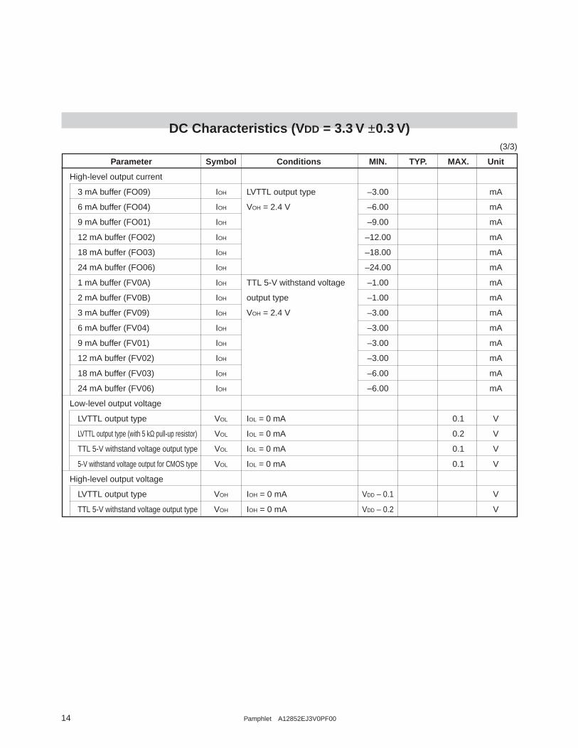
DC Characteristics (V DD = 3.3 V ±0.3 V)(3/3)
Parameter Symbol Conditions MIN. TYP. MAX. Unit
High-level output current
3 mA buffer (FO09) IOH LVTTL output type –3.00 mA
6 mA buffer (FO04) IOH VOH = 2.4 V –6.00 mA
9 mA buffer (FO01) IOH –9.00 mA
12 mA buffer (FO02) IOH –12.00 mA
18 mA buffer (FO03) IOH –18.00 mA
24 mA buffer (FO06) IOH –24.00 mA
1 mA buffer (FV0A) IOH TTL 5-V withstand voltage –1.00 mA
2 mA buffer (FV0B) IOH output type –1.00 mA
3 mA buffer (FV09) IOH VOH = 2.4 V –3.00 mA
6 mA buffer (FV04) IOH –3.00 mA
9 mA buffer (FV01) IOH –3.00 mA
12 mA buffer (FV02) IOH –3.00 mA
18 mA buffer (FV03) IOH –6.00 mA
24 mA buffer (FV06) IOH –6.00 mA
Low-level output voltage
LVTTL output type VOL IOL = 0 mA 0.1 V
LVTTL output type (with 5 kΩ pull-up resistor) VOL IOL = 0 mA 0.2 V
TTL 5-V withstand voltage output type VOL IOL = 0 mA 0.1 V
5-V withstand voltage output for CMOS type VOL IOL = 0 mA 0.1 V
High-level output voltage
LVTTL output type VOH IOH = 0 mA VDD – 0.1 V
TTL 5-V withstand voltage output type VOH IOH = 0 mA VDD – 0.2 V

15Pamphlet A12852EJ3V0PF00
AC Characteristics
The values in the table below refer to when the supply voltage of the internal gate array block is 3.3 V.
Parameter Symbol Conditions MIN. TYP. MAX. Unit
Toggle frequency ftog Internal toggle F/F (fanout = 2) 670 MHz
Propagation delay time tPD Internal gates Fanout = 1, wiring length 0 mm 94 ps
Fanout = 1, standard wiring length 131 ps
Standard load 108 ps
Fanout = 1, standard wiring length 107 ps
Standard load 94 ps
Input buffers Fanout = 1, standard wiring length 229 ps
Standard load 222 ps
Output buffer (FO01) CL = 15 pF 1396 ps
Output rise time tr Output buffer (FO01) CL = 15 pF 2391 ps
Output fall time tf Output buffer (FO01) CL = 15 pF 1872 ps
Remark Standard load: Fanout = 2, wiring length 0 mm
Internal gates,power gates,2NAND
16 Pamphlet A12852EJ3V0PF00
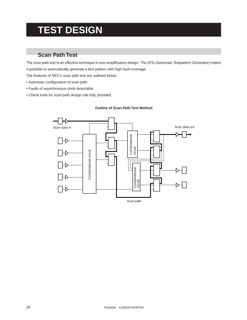
Scan data in Scan data out
Scan path
Com
bina
tiona
l circ
uit
Com
bina
tiona
l ci
rcui
tC
ombi
natio
nal
circ
uit
TEST DESIGN
Scan Path TestThe scan path test is an effective technique in test simplification design. The ATG (Automatic Testpattern Generator) makes
it possible to automatically generate a test pattern with high fault coverage.
The features of NEC's scan path test are outlined below.
• Automatic configuration of scan path
• Faults of asynchronous clock detectable
• Check tools for scan path design rule fully provided
Outline of Scan Path Test Method
17Pamphlet A12852EJ3V0PF00
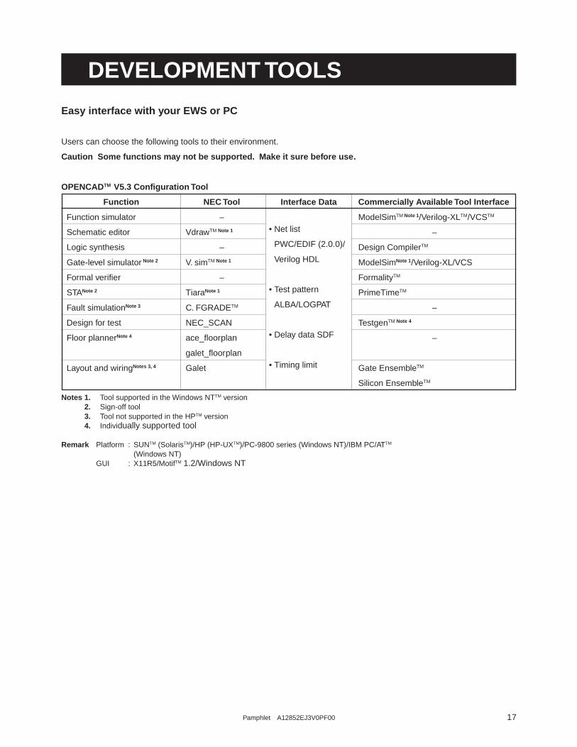
DEVELOPMENT TOOLS
Easy interface with your EWS or PC
Users can choose the following tools to their environment.
Caution Some functions may not be supported. Make it sure before use.
OPENCADTM V5.3 Configuration Tool
Function NEC Tool Interface Data Commercially Available Tool Interface
Function simulator – ModelSimTM Note 1/Verilog-XLTM/VCSTM
Schematic editor VdrawTM Note 1 –
Logic synthesis – Design CompilerTM
Gate-level simulator Note 2 V. simTM Note 1 ModelSimNote 1/Verilog-XL/VCS
Formal verifier – FormalityTM
STANote 2 TiaraNote 1 PrimeTimeTM
Fault simulationNote 3 C. FGRADETM –
Design for test NEC_SCAN TestgenTM Note 4
Floor plannerNote 4 ace_floorplan –
galet_floorplan
Layout and wiringNotes 3, 4 Galet Gate EnsembleTM
Silicon EnsembleTM
Notes 1. Tool supported in the Windows NTTM version2. Sign-off tool3. Tool not supported in the HPTM version4. Individually supported tool
Remark Platform : SUNTM (SolarisTM)/HP (HP-UXTM)/PC-9800 series (Windows NT)/IBM PC/ATTM
(Windows NT)GUI : X11R5/MotifTM 1.2/Windows NT
• Net list
PWC/EDIF (2.0.0)/
Verilog HDL
• Test pattern
ALBA/LOGPAT
• Delay data SDF
• Timing limit
18 Pamphlet A12852EJ3V0PF00
OPENCAD, Vdraw, V. sim and C. FGRADE are trademarks of NEC Corporation.
Verilog-XL, Gate Ensemble and Silicon Ensemble are trademarks of Cadence Design Systems, Inc.
ModelSim is a trademark of Model Technology Inc.
VCS, Design Compiler, Formality, PrimeTime and Testgen are trademarks of Synopsys, Inc.
Windows NT is either registered trademark or trademark of Microsoft Corporation in the United States and/or other coun-
tries.
HP and HP-UX are trademarks of Hewlett-Packard Co.
SUN and Solaris are trademarks of SUN Microsystems, Inc.
PC/AT is a trademark of IBM Corporation.
Motif is a trademark of Open Software Foundation, Inc. (OSF).
19Pamphlet A12852EJ3V0PF00
The export of this product from Japan is regulated by the Japanese government. To export this product may be prohibitedwithout governmental license, the need for which must be judged by the customer. The export or re-export of this productfrom a country other than Japan may also be prohibited without a license from that country. Please call an NEC salesrepresentative.
M8E 00. 4
The information in this document is current as of April, 2000. The information is subject to change without notice. For actual design-in, refer to the latest publications of NEC's data sheets or data books, etc., for the most up-to-date specifications of NEC semiconductor products. Not all products and/or types are available in every country. Please check with an NEC sales representative for availability and additional information.No part of this document may be copied or reproduced in any form or by any means without prior written consent of NEC. NEC assumes no responsibility for any errors that may appear in this document.NEC does not assume any liability for infringement of patents, copyrights or other intellectual property rights of third parties by or arising from the use of NEC semiconductor products listed in this document or any other liability arising from the use of such products. No license, express, implied or otherwise, is granted under any patents, copyrights or other intellectual property rights of NEC or others.Descriptions of circuits, software and other related information in this document are provided for illustrative purposes in semiconductor product operation and application examples. The incorporation of these circuits, software and information in the design of customer's equipment shall be done under the full responsibility of customer. NEC assumes no responsibility for any losses incurred by customers or third parties arising from the use of these circuits, software and information.While NEC endeavours to enhance the quality, reliability and safety of NEC semiconductor products, customers agree and acknowledge that the possibility of defects thereof cannot be eliminated entirely. To minimize risks of damage to property or injury (including death) to persons arising from defects in NEC semiconductor products, customers must incorporate sufficient safety measures in their design, such as redundancy, fire-containment, and anti-failure features.NEC semiconductor products are classified into the following three quality grades:"Standard", "Special" and "Specific". The "Specific" quality grade applies only to semiconductor products developed based on a customer-designated "quality assurance program" for a specific application. The recommended applications of a semiconductor product depend on its quality grade, as indicated below. Customers must check the quality grade of each semiconductor product before using it in a particular application. "Standard": Computers, office equipment, communications equipment, test and measurement equipment, audio
and visual equipment, home electronic appliances, machine tools, personal electronic equipmentand industrial robots
"Special": Transportation equipment (automobiles, trains, ships, etc.), traffic control systems, anti-disastersystems, anti-crime systems, safety equipment and medical equipment (not specifically designedfor life support)
"Specific": Aircraft, aerospace equipment, submersible repeaters, nuclear reactor control systems, lifesupport systems and medical equipment for life support, etc.
The quality grade of NEC semiconductor products is "Standard" unless otherwise expressly specified in NEC's data sheets or data books, etc. If customers wish to use NEC semiconductor products in applications not intended by NEC, they must contact an NEC sales representative in advance to determine NEC's willingness to support a given application.(Note)(1) "NEC" as used in this statement means NEC Corporation and also includes its majority-owned subsidiaries.(2) "NEC semiconductor products" means any semiconductor product developed or manufactured by or for@NEC (as defined above).
•
•
•
•
•
•
© NEC Corporation 1997
Document No. A12852EJ3V0PF00(3rd edition)
Date Published June 2000 N CP(K)
Printed in Japan
For further information, please contact:
G99. 11
NEC CorporationNEC Building7-1, Shiba 5-chome, Minato-kuTokyo 108-8001, JapanTel: 03-3454-1111http://www.ic.nec.co.jp/
[North & South America]
NEC Electronics Inc.2880 Scott Blvd.Santa Clara, CA 95050-2554, U.S.A.Tel: 408-588-6000
800-366-9782Fax: 408-588-6130
800-729-9288http://www.necel.com/
NEC do Brasil S.A.Electron Devices DivisionRodovia Presidente Dutra, Km 21407210-902-Guarulhos-SP BrasilTel: 55-11-6465-6810Fax: 55-11-6465-6829
[Europe]
NEC Electronics (Germany) GmbHKanzlerstr. 2,40472 DüsseldorfGermanyTel: 0211-650302Fax: 0211-6503490http://www.nec.de/
Munich OfficeArabellastr. 1781925 München, GermanyTel: 089-921003-0Fax: 089-92100315
Stuttgart OfficeIndustriestr. 370507 Stuttgart, GermanyTel: 0711-99010-0Fax: 0711-99010-19
Hannover OfficePodbielskistr. 164D-30177 Hannover, GermanyTel: 0511-33402-0Fax: 0511-33402-34
Benelux OfficeBoschdijk 187a5612 HB Eindhoven,The NetherlandsTel: 040-2445845Fax: 040-2444580
Scandinavia OfficeP.O. Box 13418322 Taeby, SwedenTel: 08-6380820Fax: 08-6380388
NEC Electronics (UK) LimitedCygnus House, Sunrise Park Way,Milton Keynes, MK14 6NP, U.K.Tel: 01908-691-133Fax: 01908-670-290
NEC Electronics (France) S.A.9, rue Paul Dautier-BP 18778142 Velizy-Villacoublay CédexFranceTel: 01-30-67-58-00Fax: 01-30675899
Madrid OfficeJuan Esplandiu, 1528007 Madrid, SpainTel: 91-504-2787Fax: 91-504-2860
NEC Electronics Italiana s.r.l.Via Fabio Filzi, 25/A,20124 Milano, ItalyTel: 02-667541Fax: 02-66754299
[Asia & Oceania]
NEC Electronics Hong Kong Limited12/F., Cityplaza 4,12 Taikoo Wan Road, Hong KongTel: 2886-9318Fax: 2886-9022/9044
Seoul Branch10F, ILSONG Bldg., 157-37,Samsung-Dong, Kangnam-KuSeoul, the Republic of KoreaTel: 02-528-0303Fax: 02-528-4411
NEC Electronics Taiwan Ltd.7F, No. 363 Fu Shing North RoadTaipei, Taiwan, R. O. C.Tel: 02-2719-2377Fax: 02-2719-5951
NEC Electronics Singapore Pte. Ltd.101 Thomson Road #04-01/05United Square, Singapore 307591Tel: 65-253-8311Fax: 65-250-3583