on the design of a photonic network-on-chipluca/research/shacham_nocs07.pdf ·...
TRANSCRIPT

On the Design of a Photonic Network-on-Chip
Assaf ShachamColumbia University
Dept. of Electrical Engineering500 W 120th St.,
New York, NY [email protected]
Keren BergmanColumbia University
Dept. of Electrical Engineering500 W 120th St.,
New York, NY [email protected]
Luca P. CarloniColumbia University
Dept. of Computer Science1214 Amsterdam Ave.,New York, NY [email protected]
Abstract
Recent remarkable advances in nanoscale silicon-photonic integrated circuitry specifically compatible withCMOS fabrication have generated new opportunities forleveraging the unique capabilities of optical technologiesin the on-chip communications infrastructure. Based onthese nano-photonic building blocks, we consider a pho-tonic network-on-chip architecture designed to exploit theenormous transmission bandwidths, low latencies, and lowpower dissipation enabled by data exchange in the opti-cal domain. The novel architectural approach employs abroadband photonic circuit-switched network driven in adistributed fashion by an electronic overlay control networkwhich is also used for independent exchange of short mes-sages. We address the critical network design issues forinsertion in chip multiprocessors (CMP) applications, in-cluding topology, routing algorithms, path-setup and tear-down procedures, and deadlock avoidance. Simulationsshow that this class of photonic networks-on-chip offers asignificant leap in the performance for CMP intrachip com-munication systems delivering low-latencies and ultra-highthroughputs per core while consuming minimal power.
1. Introduction
A major design paradigm shift is currently impactinghigh-performance microprocessors as critical technologiesare simultaneously converging on fundamental performancelimits. Essentially, the scaling in transistor speeds and in-tegration densities can no longer drive the expected con-gruent multiples in computation performance [14]. Ac-celerated local processing frequencies have clearly reacheda point of diminishing returns: further increases in speedlead to tighter bounds on the logic coherently accessed on-chip [3, 13] and the associated power dissipation is exac-erbated in an exponential fashion [2, 22]. Evidence of this
trend is unmistakable as practically every commercial man-ufacturer of high-performance processors is currently intro-ducing products based on multi-core architectures: AMDOpteron, Intel Montecito, Sun Niagara, and IBM Cell andPower5. These systems aim to optimize performance perwatt by operating multiple parallel processors at lower clockfrequencies.
Clearly, within the next few years, performance gainswill come from increases in the number of processor coresper chip [14, 22], leading to the emergence of a key bottle-neck: the global intrachip communications infrastructure.Perhaps the most daunting challenge to future systems isto realize the enormous bandwidths capacities and stringentlatency requirements when interconnecting a large numberof processing cores in a power efficient fashion.
Low latency, high data-rate, on-chip interconnection net-works have therefore become a key to relieving one ofthe main bottlenecks to CMP system performance. Sig-nificant research activity has recently focused on intra-chip global communication using packet-switched micro-networks [1,6,10,11,19]. These so-called networks-on-chip(NoC) are made of carefully-engineered links and representa shared medium that is highly scalable and can provideenough bandwidth to replace many traditional bus-basedand/or point-to-point links. However, with a fixed upperlimit to the total chip power dissipation, and the communi-cations infrastructure emerging as a major power consumer,performance-per-watt is becoming the most critical designmetric for the scaling of NoCs and CMPs. It is not clear howelectronic NoCs will continue to satisfy future communica-tion bandwidths and latency requirements within the powerdissipation budget.
Photonic interconnection networks offer a potentiallydisruptive technology solution with fundamentally lowpower dissipation that remains independent of capacitywhile providing ultra-high throughputs and minimal accesslatencies. One of the main drivers for considering photonicNoCs is the expected reduction in power expended on in-

trachip communications. The key power saving rises fromthe fact that once a photonic path is established, the dataare transmitted end to end without the need for repeating,regeneration or buffering. In electronic NoCs, on the otherhand, messages are buffered, regenerated and then transmit-ted on the inter-router links several times en route to theirdestination. In previous work [27] we provided a detailedpower analysis of a photonic NoC, and compared it to anelectronic NoC designed to provide the same bandwidth tothe same number of cores. The compelling conclusion ofthe study was that the power expended on intrachip com-munications can be reduced by two orders of magnitudewhen high-bandwidth communications is required amongthe cores.
In this paper we explore the design and performance ofan optical NoC that can capitalize on the enormous capac-ity, transparency, low latency, and fundamentally low powerconsumption of photonics. The construction of this opticalNoC is based on remarkable advances made over the pastseveral years in silicon photonics that have yielded unprece-dented control over device optical properties. Fabricationcapabilities and integration with commercial CMOS chipmanufacturing that are now available open new exciting op-portunities [8].
The optical NoC building blocks are nanoscale photonicintegrated circuits (PICs) that employ optical microcavities,particularly those based on ring resonator structures shapedfrom photonic waveguides which can easily be fabricatedon conventional silicon and silicon-on-insulator (SOI) sub-strates. This new class of small footprint PICs can realizeextremely high interconnection bandwidths which consumeless power and introduce less latency than their contempo-rary bulk counterparts. Compatibility with existing CMOSfabrication systems and the juxtaposition with silicon elec-tronics enable direct driving, controllability, and the inte-gration of these optical networks with processor cores andother silicon-based systems. By using photonic NoCs weexploit the unique advantages in terms of bandwidth, la-tency, and energy that have made photonics ubiquitous inlong-haul transmission systems for on-chip interconnectionnetworks.
High speed optical modulators, capable of performingswitching operations, have been realized using these ringresonator structures [29, 30] (see Fig. 1) or the free carrierplasma dispersion effect in Mach-Zhender geometries [21].The integration of modulators, waveguides and photodetec-tors with CMOS integrated circuits for off-chip communi-cation has been reported and recently became commerciallyavailable [8]. On the receiver side, SiGe-based photode-tectors and optical receivers were fabricated with reportedhigh efficiencies [9]. Finally, low-loss waveguide technol-ogy with crossovers and a fairly aggressive turn radii hasmade some remarkable recent advances and the enabling
Figure 1. A silicon ring resonator [30] (left)and a 10 Gb/s eye-diagram from a siliconmodulator [8] (right)
technologies are currently available [4, 15].For the first time, the integration of a fully functional
photonic system on a VLSI electronic die can be realisti-cally envisioned, and, in particular, the photonic elementsnecessary to build a complete photonic NoC (dense waveg-uides, switches, modulators, and detectors) are now viablefor integration on a single silicon chip. Fig. 1 shows pub-lished examples of some of the silicon electro-optic devicesmentioned above.
In this paper we present a novel architecture for a pho-tonic network-on-chip, and discuss its advantages while ad-dressing critical design challenges. Network topology, rout-ing algorithms, and flow control are discussed in detail. Wedeveloped an event-driven network simulator to quantita-tively evaluate design aspects such as deadlock avoidanceand recovery, path diversity and flow control. The con-clusion of the quantitative study demonstrates the poten-tial performance leap offered by the integration of a pho-tonic micro-network within high-performance multi-coresystems.
2 Architecture Overview
The photonic NoC architecture employs a hybrid de-sign, synergistically combining an optical network for bulkmessage transmission and an electronic network, with thesame topology, for distributed control and short messageexchange.
While photonic technology offers unique advantages interms of energy and bandwidth, two necessary functions forpacket switching, namely buffering and processing, are verydifficult to implement. Electronic NoCs which have manyadvantages in flexibility and abundant functionality tend toconsume high power which scales up with the transmittedbandwidth [22]. The hybrid approach deals with this prob-lem by employing two layers:
1. A photonic interconnection network, comprised of sil-icon broadband photonic switches interconnected bywaveguides, is used to transmit high bandwidth mes-sages.
2. An electronic control network, topologically identicalto the photonic network, is used to control the pho-tonic network and for the exchange of short controlmessages.
Every photonic message transmitted is preceded by an elec-tronic control packet (a path-setup packet) which is routedin the electronic network, acquiring and setting-up a pho-tonic path for the message. Buffering of messages is im-possible in the photonic network, as there are no photonicequivalents for storage elements (e.g. flip-flops, registers,RAM). Hence, buffering, if necessary, only takes place forthe electronic packets during the path-setup phase. The pho-tonic messages are transmitted without buffering once thepath has been acquired. This approach has many similaritieswith optical circuit switching, a technique used to establishlong lasting connections between nodes in the optical inter-net core.
The main advantage of using photonic paths relies on aproperty of the photonic medium, known as bit-rate trans-parency [25]. Unlike routers based on CMOS technologythat must switch with every bit of the transmitted data, lead-ing to a dynamic power dissipation that scales with the bitrate [22], photonic switches switch on and off once per mes-sage, and their energy dissipation does not depend on the bitrate. This property facilitates the transmission of very highbandwidth messages while avoiding the power cost that istypically associated with them in traditional electronic net-works. Another attractive feature of optical communica-tions results from the low loss in optical waveguides: at thechip scale, the power dissipated on a photonic link is com-pletely independent of the transmission distance. Energydissipation remains essentially the same whether a messagetravels between two cores that are 2 mm or 2 cm apart. Fur-thermore, low loss off-chip interconnects such as opticalfibers enable the seamless scaling of the optical commu-nications infrastructure to multi-chip systems.
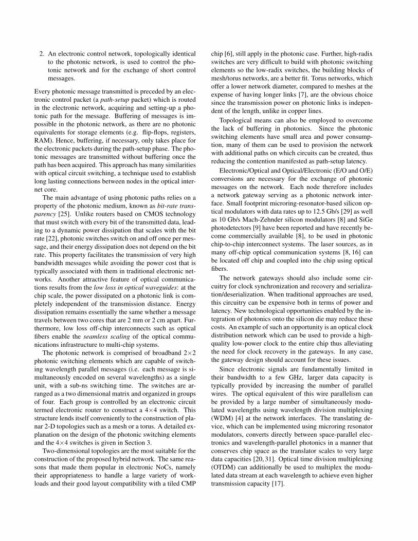
The photonic network is comprised of broadband 2×2photonic switching elements which are capable of switch-ing wavelength parallel messages (i.e. each message is si-multaneously encoded on several wavelengths) as a singleunit, with a sub-ns switching time. The switches are ar-ranged as a two dimensional matrix and organized in groupsof four. Each group is controlled by an electronic circuittermed electronic router to construct a 4×4 switch. Thisstructure lends itself conveniently to the construction of pla-nar 2-D topologies such as a mesh or a torus. A detailed ex-planation on the design of the photonic switching elementsand the 4×4 switches is given in Section 3.
Two-dimensional topologies are the most suitable for theconstruction of the proposed hybrid network. The same rea-sons that made them popular in electronic NoCs, namelytheir appropriateness to handle a large variety of work-loads and their good layout compatibility with a tiled CMP
chip [6], still apply in the photonic case. Further, high-radixswitches are very difficult to build with photonic switchingelements so the low-radix switches, the building blocks ofmesh/torus networks, are a better fit. Torus networks, whichoffer a lower network diameter, compared to meshes at theexpense of having longer links [7], are the obvious choicesince the transmission power on photonic links is indepen-dent of the length, unlike in copper lines.
Topological means can also be employed to overcomethe lack of buffering in photonics. Since the photonicswitching elements have small area and power consump-tion, many of them can be used to provision the networkwith additional paths on which circuits can be created, thusreducing the contention manifested as path-setup latency.
Electronic/Optical and Optical/Electronic (E/O and O/E)conversions are necessary for the exchange of photonicmessages on the network. Each node therefore includesa network gateway serving as a photonic network inter-face. Small footprint microring-resonator-based silicon op-tical modulators with data rates up to 12.5 Gb/s [29] as wellas 10 Gb/s Mach-Zehnder silicon modulators [8] and SiGephotodetectors [9] have been reported and have recently be-come commercially available [8], to be used in photonicchip-to-chip interconnect systems. The laser sources, as inmany off-chip optical communication systems [8, 16] canbe located off chip and coupled into the chip using opticalfibers.
The network gateways should also include some cir-cuitry for clock synchronization and recovery and serializa-tion/deserialization. When traditional approaches are used,this circuitry can be expensive both in terms of power andlatency. New technological opportunities enabled by the in-tegration of photonics onto the silicon die may reduce thesecosts. An example of such an opportunity is an optical clockdistribution network which can be used to provide a high-quality low-power clock to the entire chip thus alleviatingthe need for clock recovery in the gateways. In any case,the gateway design should account for these issues.
Since electronic signals are fundamentally limited intheir bandwidth to a few GHz, larger data capacity istypically provided by increasing the number of parallelwires. The optical equivalent of this wire parallelism canbe provided by a large number of simultaneously modu-lated wavelengths using wavelength division multiplexing(WDM) [4] at the network interfaces. The translating de-vice, which can be implemented using microring resonatormodulators, converts directly between space-parallel elec-tronics and wavelength-parallel photonics in a manner thatconserves chip space as the translator scales to very largedata capacities [20, 31]. Optical time division multiplexing(OTDM) can additionally be used to multiplex the modu-lated data stream at each wavelength to achieve even highertransmission capacity [17].

The energy dissipated in these large parallel structures isnot small, but it is still smaller then the energy consumedby the wide busses and buffers currently used in NoCs:the network gateway interface and corresponding E/O andO/E conversions occur once per node in the proposed sys-tem, compared to multiple ports at each router in electronicequivalent NoCs [27].
The employment of 4×4 switches places a unique con-straint on the placement of the gateways. Since the photonicswitches do not have a fifth port for injection/ejection thegateways require specially designed access point to permitinjection and ejection of messages without interfering withpass-through traffic. The gateway placement policy and thedesign of access points will be described in Subsection 3.2.
2.1 Life of a Packet on the Photonic NoC
Finally, to illustrate the operation of the proposed NoCwe describe the typical chain of events in the transmissionof a message between two terminals. In this example, awrite operation takes place from a processor in node A to amemory address located at node B. Both are arbitrary nodesconnected through the photonic NoC.
As soon as the write address is known, possibly evenbefore the contents of the message are ready, a path-setuppacket is sent on the electronic control network. The packetincludes information on the destination address of node B,and perhaps additional control information such as priority,flow id, or other. The control packet is routed in the elec-tronic network, reserving the photonic switches along thepath for the photonic message which will follow it. At ev-ery router in the path, a next-hop decision is made accordingto the routing algorithm used in the network.
When the path-setup packet reaches the destination nodeB, the photonic path is reserved and is ready to route themessage. Since the photonic path is completely bidirec-tional a fast light pulse can then be transmitted onto thewaveguide, in the opposite direction (from the destinationnode B to the source node A), signaling to the source thatthe path is open (using a technique presented similar toRef. [26]). The photonic message transmission then beginsand the message follows the path from switch to switch untilit reaches its destination. Since special hardware and addi-tional complexity are required to transmit and extract thecounter-directional light pulses, an alternative approach canbe used: This approach is based on transmitting the messagewhen the path is assumed to be ready according to the max-imum expected path reservation latency. While this schemedoes not utilize the network resources as well as the firstone, it requires less hardware resources.
After the message transmission is completed a path-teardown packet is finally sent to release the path for usageby other messages. Once the photonic message has been
Figure 2. Photonic switching element: (a)OFF state: a passive waveguide crossover.(b) ON state: light is coupled into rings andforced to turn
received and checked for errors, a small acknowledgementpacket may be sent on the electronic control network, tosupport guaranteed-delivery protocols.
In the case where a path-setup packet is dropped in therouter due to congestion, a path-blocked packet is sent inthe reverse direction, backtracking the path traveled by thepath-setup packet. The path-blocked packet releases the re-served switches and notifies the node attempting transmis-sion that its request was not served.
3 Network Design
In this section we describe in detail the proposed imple-mentation of the photonic network and its electronic controllayer, touching some key implementation issues.
3.1 Building Blocks
The fundamental building block of the photonic net-work is a broadband photonic switching element (PSE),based on a ring-resonator structure. The switch is, inessence, a waveguide intersection, positioned between tworing resonators (Fig. 2). The rings have a certain reso-nance frequency, derived from material and structural prop-erties. In the OFF state, when the resonant frequency of therings is different from the wavelength (or wavelengths) onwhich the optical data stream is modulated, the light passesthrough the waveguide intersection uninterrupted, as if it isa passive waveguide crossover (Fig. 2a). When the switchis turned ON, by the injection of electrical current into p-ncontacts surrounding the rings, the resonance of the ringsshifts such that the transmitted light, now in resonance, iscoupled into the rings making a right angle turn (Fig. 2b),thus creating a switching action.
Photonic switching elements and modulators based onthe forementioned effect have been realized in silicon anda switching time of 30 ps has been experimentally demon-strated [29]. Their merit lies mainly in their extremely smallfootprint, approximately 12µm ring diameter and their low
Figure 3. 4×4 switch. Four photonic switch-ing elements (PSE) controlled by an elec-tronic router (ER).
power consumption: less than 0.5 mW, when ON. Whenthe switches are OFF, they act as passive devices and con-sume nearly no power. Ring-resonator based switches ex-hibit good crosstalk properties (> 20 dB), and a low in-sertion loss, approximately 1.5 dB [28]. These switchesare typically narrow-band, but advanced research efforts arenow undergoing to fabricate wideband structures capable ofswitching several wavelengths simultaneously, each modu-lated at tens of Gb/s. It is also reasonable to assume that theloss figures can be improved with advances in fabricationtechniques.
The PSEs are interconnected by silicon waveguides, car-rying the photonic signals, and are organized in groupsof four. Each quadruplet, controlled by an electronic cir-cuit termed an electronic router, forms a 4×4 switch (Fig.3). The 4×4 switches are, therefore, interconnected by theinter-PSE waveguides and by metal lines connecting theelectronic routers. Control packets (e.g. path-setup) are re-ceived in the electronic router, processed and sent to theirnext hop, while the PSEs are switched ON and OFF ac-cordingly. Once a packet completes its journey through asequence of electronic routers, a chain of PSEs is ready toroute the optical message. Owing to the small footprint ofthe PSEs and the simplicity of the electronic router, whichonly handles small control packets, the 4×4 switch can havea very small area. Based on the size of the microring res-onator devices [29], and the minimal logic required to im-plement the electronic router, we estimate this area at 70 µm× 70 µm.
A keen observer will notice that the 4× 4 switch in Fig.3 is blocking. For example, a message routed from Southto East will block message requests from West to South andfrom East to North. In general, every message which makesa wide turn (i.e. a turn involving 3 PSEs) may block twoother message requests that attempt to make wide turns.Messages that make narrow turns (e.g. South to West)
and messages that are routed straight through do not blockother messages and cannot be blocked. To limit the block-ing problem U-turns within the switches are forbidden. Theblocking relationships between messages are summarizedin Table 1.
Table 1. Inter-message blocking relationshipsin the 4×4 photonic switch
Current Blocked Blockedmessage message I message II
North→West East→North West→SouthWest→South North→West South→EastEast→North South→East North→WestSouth→East West→South East→North
Being nonblocking is an important requirement from anatomic switch in an interconnection network. Nonblock-ing switches offer improved performance and simplify net-work management and routing. However, constructing anonblocking 4 × 4 switch with the given photonic buildingblocks requires an exceedingly complex structure. This willhave a negative impact on the area and, more importantly,the optical signal integrity, as each PSE hop can introduceadditional loss and crosstalk. The design choice is, there-fore, to use the blocking switch, because of its compactness,and bear its blocking properties in mind when designing thetopology and a routing algorithm.
It is worth mentioning that different PSE groupingschemes can be used, where the directions of the waveg-uides are flipped, causing the blocking properties to slightlychange. One possible scheme is to group the PSEs as amirror-image of the current grouping scheme, where the di-rections of all waveguides are flipped. The analysis of thiscase is identical to the original grouping scheme. In yet an-other scheme, the direction of only one pair of waveguidesis flipped (either the vertical or the horizontal). In this caseeach turning message may block one other message.
A related constraint, resulting from the switch structure,concerns the local injection/ejection port. Typically, 2-Dmesh/torus NoCs use 5×5 switches, where one port is ded-icated for local injection and ejection of packets. A 5×5switch, while very simple to implement as an electronictransistor-based crossbar, is quite difficult to construct us-ing 2×2 photonic switching elements. The injection andejection of packets is, therefore, done through one of the4 existing ports, thus blocking it for through traffic. Thisdesign decision places constraints on the topology, as de-scribed in the next subsection.

Figure 4. A 4-ary 2-D folded torus network(thick lines and dark ovals), access points(thin lines and light ovals), and 16 gateways(rectangles). One access point is shaded andenlarged.
3.2 Topology
The topology of choice in our design reflects the charac-teristics of the entire system - a chip multiprocessor (CMP),where a number of homogeneous processing cores are in-tegrated as tiles on a single die. The communication re-quirements of a CMP are best served by a 2-D regulartopology such as a mesh or a torus [24]. These topologiesmatch well the planar, regular layout of the CMP and theapplication-based nature of the traffic - any program run-ning on the CMP may generate a different traffic pattern [7].As mentioned above, a regular 2-D topology requires 5×5switches which are overly complex to implement using pho-tonic technology. We therefore use a folded torus topologyas a base and augment it with access points for the gate-ways. An example of a 4×4 folded torus network, with theaugmenting access points appears in Fig. 4.
The access points for the gateways are designed withtwo goals in mind: (1) to facilitate injection and ejectionwithout interference with the through traffic on the torus,and (2) to avoid blocking between injected and ejected traf-fic which may be caused by the switches internal blocking.Injection-ejection blocking can be detrimental to the perfor-mance and may also cause deadlocks. The access points aredesigned such that gateways (i.e. the optical transmittersand receivers) are directly connected to a 4×4 switch (thegateway switch), through its West port (see Fig. 4). We as-sume, without loss of generality, that all the gateways areconnected to the same port in their respective switches.
To avoid internal blocking a set of injection-ejectionrules must be followed: injected messages make a turn atthe gateway switch, according to their destination, and thenenter the torus network through an injection switch. Mes-sages are ejected from the torus network when they arrive
Figure 5. Example of a deadlock-avoidingpath on the augmented folded torus network.
to the ejection switch associated with their final destina-tion. The ejection switches are located on the network, atthe same row as the gateway switch, and this is the placewhere the ejecting messages turn. Finally, ejected messagespass through the gateway switch without making turns. Anexample of a path with the different kinds of switches isillustrated in Fig. 5.
Since torus networks are edge-symmetric [7], injectioncan be done at any port of the gateway switch, as long asthe structure of the access point is rotated accordingly. Anexplanation on how this structure reduces contentions andavoids deadlocks is provided in Section 5.
The design of the access points contributes to a largerswitch count in the network, as every access point requires 3additional switches. However, each switch has rather smallfootprint and power dissipation, thus making the overallpenalty minimal compared to the global power savings en-abled by the photonic design [27].
A network designer may take advantage of the smallfootprint to improve the performance by increasing path di-versity. Whenever the path-setup packet faces contentionit is buffered in the electronic router until the blocking iscleared. The torus network can be augmented with addi-tional paths, without changing the number of access points,so that the probability of blocking is lowered and the path-setup latency is, accordingly, reduced. Owing to the smallfootprint of the switches, the simplicity of the routers, andthe fact that the PSEs only consume power when they causemessages to turn, the power and area cost of adding parallelpaths is not large. The latency penalty that results from theincreased hop-count should be balanced against the latencyreduction achieved by mitigating contention. This study isperformed in Section 7.
3.3 Routing
Dimension order routing is a simple routing algorithmfor mesh and torus networks. It requires minimal logic in

the routers and, being an oblivious algorithm, it does notrequire the routers to maintain a state or exchange addi-tional information between them. We use XY dimensionorder routing on the torus network, with a slight modifi-cation required to accommodate the injection/ejection rulesdescribed in Subsection 3.1 above.
Each message is encoded with 3 addresses: 2 intermedi-ate addresses and a final address, encapsulated within oneanother. The first intermediate address directs the messageto the injection switch on torus network, thus causing themessage to make the turn at the gateway switch, as requiredby the injection rules (see Fig. 5). The message is thenrouted on the torus, using plain XY dimension order rout-ing, to the second intermediate address, the ejection switch(in the final destinations row, but one column away fromit). Only then the final address is decapsulated and the mes-sage is forwarded to the destination gateway, where it ar-rives without having to turn, according to the ejection rules.The address encapsulation mechanism relieves the routersfrom processing system-scale considerations when settingup a path and preserves the simplicity of dimension orderrouting in the torus network.
When the torus network is path-diversified [7], (orpath-multiplied, where several parallel lanes exist in eachrow/column), the address encapsulation mechanism can beused to take advantage of the path diversity while preservingthe simplicity and obliviousness of dimension order routing.The encoding of the intermediate addresses can be donewith the goal of balancing the load between parallel lanes,thus reducing the contention. According to this method thefirst intermediate address will be an injection switch on oneof the lanes, as chosen by the gateway. The ejection, amongthe several parallel lanes, is also chosen by the gateway andencoded on the second intermediate address. The final ad-dress, of course, does not change. The selection of inter-mediate addresses is equivalent to choosing, at random, oneamong several torus sub-networks thus balancing the loadamong them.
In Section 7 we use the load-balancing approach whenevaluating the effect of path diversity. Alternative interme-diate address selection methods can be used such as restrict-ing one lane to high priority traffic or allocating lanes tosources or designated flows.
3.4 Flow Control
The flow control technique in the network greatly differsfrom common NoC flow control methods. The dissimilar-ity stems from the fundamental differences between elec-tronic and photonic technologies and mainly from the factthat memory elements (such as flip-flops and SRAM) can-not be used to buffer messages or even to delay them whileprocessing is done. Electronic control packets are, there-
Figure 6. Qualitative timing diagram of a suc-cessful message setup (left) and a blockedsetup request (right)
fore, exchanged to acquire photonic paths, and the data areonly transmitted, with a very high bandwidth, once the pathhas been acquired.
The path acquisition procedure requires the path-setuppacket to travel a number of electronic routers and undergosome processing in each hop. Additionally, the packet mayexperience blocking at certain points in its path further con-tributing to the setup latency. Once the path is acquired,the transmission latency of the optical data is very shortand depends only on the group velocity of light in a sili-con waveguide: approximately 6.6× 10⁷ m/s, or 300 ps fora 2-cm path crossing a chip [15]. The network can, there-fore, be perceived as a fast circuit-switched network, wherethe path-setup latency is much longer than the transmissionlatency. On the other hand, path-setup latency is still on theorder of nanoseconds, a very short time compared to typicalmillisecond-setup-time circuit-switched networks. Hence,it can still be considered fast and can emulate packet switch-ing traffic when packets are fairly large. The timing diagramin Fig. 6 illustrates the timing discrepancy.
The decision regarding the minimal size of the data unitexchanged on the photonic network must, therefore, takeinto account the path-setup latency. Exchange of smallpackets, such as memory read requests or cache-coherencysnoop messages, for example, is clearly inefficient. The ex-change of memory pages or long cache lines, instead, canutilize the photonic network much better. A good exam-ple is represented by the IBM/Toshiba/Sony Cell Broad-band Engine processor where the bulk of the interconnec-tion network traffic is made of DMA transactions [18]. Forother applications, long lasting connections can be set upbetween processors that are expected to communicate fre-quently, providing a high-bandwidth link with minimal la-tency and low power consumption on which packets of anysize can be transmitted.
The hybrid network architecture addresses the smallpackets exchange problem elegantly. Control messages thatcarry no data and are of a very small size, such as read re-
quests, write acknowledgments, or cache snoops, can be ex-changed on the control network which is, in essence, a low-bandwidth electronic NoC. These control messages are notexpected to present a challenge for the control network be-cause of their small size and will not require large resourcesin terms of additional circuitry or power.
Further, some applications, such as cryptanalysis for ex-ample, are characterized with exchange of very small datamessages without any locality that can be exploited forgrouping or speculative fetching. A CMP featuring the pro-posed hybrid architecture can utilize the electronic controlnetwork to exchange these massages at a reasonable perfor-mance.
In any case, it is of interest to study the optimal photonicmessage size in a given implementation of the network.This depends on the network size, on the latency of theindividual components (routers, photonic links, electroniclinks, etc.), and on the bandwidth of the gateways. Whileone would want to minimize the setup overhead by usinglarge messages, their size should be kept small enough toallow for good flexibility and link utilization. In Section 6we analyze the optimal message size for the proposed net-work using an event-driven simulation model.
4 Simulation Setup
A key stage in the development of the ideas presentedabove is their functional validation using simulation. Thecorrectness of the distributed path-setup procedure and therouting algorithm, for example, must be verified in a soft-ware environment that models accurately the network archi-tecture. A quantitative performance study, using a varietyof traffic loads, should also be carried out to evaluate algo-rithms, topologies and flow control techniques. This perfor-mance study also requires an accurate simulation model.
We developed POINTS (Photonic On-chip Interconnec-tion Network Traffic Simulator), an event-driven simula-tor based on OMNeT++ [23]. OMNeT++ is an opensource simulation environment that provides good supportfor modular structures, message-based communications be-tween modules, and accurate modeling of physical layerfactors such as delay, bandwidth and error rate.
The implemented model is highly parameterized to allowfor a broad exploration of the design space. For the studyin this paper the following design point is chosen: The sys-tem is a 36-core chip multiprocessor (CMP), organized in a6×6 planar layout, built in a future 22 nm CMOS processtechnology. The chip size is assumed to be 20 mm along itsedge, so each core is 3.3 mm× 3.3 mm in size. The networkis a 6×6 folded-torus network augmented with 36 gatewayaccess points (Fig. 4 presents a similar, albeit smaller, net-work), so it uses 144 switches, organized as 12×12. Theelectronic routers, each located at a center of a switch, are
spaced by 1.67 mm and the PSEs (576 are used) are spacedby 0.83 mm.
The area and spacing considerations dictate the timingparameters of the network, as modeled in simulation. Weassume a propagation velocity of 15.4 ps/mm in a siliconwaveguide for the photonic signals [26] and 131 ps/mm inan optimally repeatered wire at 22 nm for the electronic sig-nals traveling between electronic routers [12]. The inter-PSE delay and inter-router delay are, therefore, 13 ps and220 ps respectively. The PSE setup time is assumed to be1 ns and the router processing latency is 600 ps, or 3 cyclesof a 5GHz clock.
Message injection processes in NoC simulation modelsare typically Bernoulli or modulated-Bernoulli processes,which work well with packet-switched slotted network.Since our architecture resembles circuit-switching morethan packet- switching, we model the inter-message gap asan exponential random variable with a parameter µIMG. Inthe simulation reported in this paper we use uniform traf-fic. While this traffic pattern does not necessarily model theactual loads presented to the network in a CMP, it serveswell as an initial measurement technique to demonstrate thecapacity of the network and as a reference to use in futuremeasurements.
In the following sections we describe three simulation-based studies performed using POINTS.
5 Dealing With Deadlock
Deadlock in torus networks has been studied exten-sively. When dimension order routing is used, no channel-dependency cycles are formed between dimensions, sodeadlock involving messages traveling in different dimen-sions cannot occur [7]. Virtual channel flow control hasbeen shown to be successful in eliminate intra-dimensiondeadlocks [5] and make dimension order routing deadlockfree. Both these proofs assume that each router in the torusnetwork is internally nonblocking.
As mentioned in Section 3, this is not the case in ournetwork. Area and technology constraints lead us to usea 4×4 switch which has some internal blocking betweenmessages. We recall that every wide turn in the switchmay block two other wide turns. Messages that make nar-row turns and messages that pass straight through do notblock other messages and cannot be blocked, and U-turnsare forbidden. Therefore, we must evaluate the topology,find when deadlocks may occur, and develop solutions toavoid them. The injection-ejection are explained in Section3 and illustrated in Fig. 5. They include the separation ofinjection and ejection to different switches so that turns thatmay block other messages cannot occur in the same switch.To prove this we inspect each of the 3 switches comprisingthe access point:

Figure 7. Gateway (a), injection (b), and ejec-tion (c) switches. All possible message-pathsare marked to demonstrate that no blockinginteractions occur
• Gateway switch: Injected messages are required tomake a turn towards the injection switches. Ejectedmessages arrive from the ejection message and passstraight through. Therefore, blocking cannot happen.
• Injection switch: messages already traveling on thetorus network do not turn to the injection paths, so noblocking interactions exist between them and the in-jected messages.
• Ejection Switch: messages may arrive only from thetorus network and they either turn for ejection or con-tinue straight through. Since no messages arrive fromthe gateway switch, none of the blocking interactionsmay happen.
In Fig. 7 the three switches are shown with all the possiblepaths marked on them. The reader is invited to verify thatnone of the internal blocking scenarios, listed in Table 1,occur.
Even though injection-ejection blockings are completelyavoided, and so are the associated performance penalty andpossible deadlocks, the problem of intra-dimensional block-ing of dimension order routing still remains. The acceptedsolution for this problem is virtual channel flow control [5]where the channel dependencies are removed by splittingthe physical channel to several virtual channels that com-pete with each other for router bandwidth. This approach isdifficult to implement in a circuit-switched network wherethe channel bandwidth cannot be divided between severalcircuits.
Hence, in our network we solve the intra-dimensionaldeadlock problem using path-setup timeouts. When a path-setup packet is sent, the gateway sets a timer to a pre-defined time. When the timer expires, a terminate-on-timeout packet is sent following the path-setup packet. Thetimeout packet follows the path acquired by the path-setuppacket until it reaches the router where it is blocked. At thatrouter, the path-setup packet is removed from the queue anda path-blocked packet is sent on the reverse path, notify-ing the routers that the packet was terminated and the path
should be freed. If a deadlock has occurred, the system re-covers from it at that point. While this method suffers fromsome inefficiency because paths and gateway injection portsare blocked for some time until they are terminated withouttransmitting, it guarantees deadlock-recovery.
In another possible scenario, the path-setup packet is notdeadlocked but merely delayed and it reaches its destina-tion while the timeout packet is en-route. In these casesthe timeout packet reaches the destination gateway whereit is ignored and discarded, and the path is acquired as ifthe timeout had not expired. This procedure has been testedin extensive simulations and has shown to be effective inresolving deadlocks.
6 Optimizing Message Size
In order to maintain the network efficiency as well as itsflexibility and link utilization the message duration shouldbe carefully picked. If too large messages are used, then linkutilization is compromised as well as latency when mes-sages are queued in the gateway for a long time while otherlong messages are transmitted. On the other hand, if mes-sages are too small, then the relative overhead of the path-setup latency becomes too large and efficiency is degraded.
Of course, there is no technical reason preventing usfrom granting full freedom in message-sizing to each node,but this may cause starvation and unfairness. In this sectionwe study the optimal size with respect to the overhead in-curred in the path-setup process under the assumption thatit is constant across all messages.
We define the overhead ratio as:
ρ =Tpath−reservation
Tmessage−duration
where Tpath−reservation is the time between the trans-mission of the path-setup packet and the transmission ofthe path-teardown packet, and Tmessage−duration is thetime during which actual transmission takes place, corre-sponding to the size of the message (see Fig. 6). Thesmaller the value of ρ, the higher the network efficiency.In Fig. 8 we plot ρ as a function of the path length andTmessage−duration, for a completely unloaded network. Inthis simulation messages of different sizes, addressed to alldestination in the network, are injected at node (0,0), whileall the other nodes do not transmit. No generality is lostwhen we inject from only a single node because of the edge-symmetry of the torus network.
The optimal message size is the smallest size which doesnot exceed a certain overhead ratio. As an arbitrary limit foran unloaded network we set the maximum allowed over-head to 20%. The maximum allowed overhead ratio is,therefore, ρ=1.25. In Fig. 8, where the 20% overhead lineappears as a dashed line, we can see that the limit is met by

Figure 8. Overhead ratio as a function ofpath-length and message duration in a un-loaded 12×12 torus network
messages with duration larger than 50 ns, for the longestpath (13 hops). We therefore pick 50 ns to be the mes-sage duration in the network and use this duration in therest of the simulations. It is worth mentioning that thanksto the huge bandwidth that can be transmitted in the pho-tonic waveguides and the broadband switches (see Section2), the amount of data that can be transmitted in 50 ns can bemore than 2 KBytes, supporting the exchange of full mem-ory pages or large DMA transactions.
Naturally the overhead will be larger when the networkbecomes loaded with traffic from other nodes, as path acqui-sition is expected to take longer due to blocking. To evalu-ate the effect of congestion on the message setup overheadwe transmit 50-ns messages, from all nodes, with uniformlydistributed addresses. The load on the network is managedby controlling the distribution parameter of the exponen-tially distributed inter-message gap (µIMG). The load of-fered (α) to the network is then given as:
α =Tmessage−duration
Tmessage−duration + 1µIMG
At the limit of constant transmission by all sources( 1µIMG
→ 0) the offered load approaches 1, and when theinter-message gap is very large ( 1
µIMG→ ∞) the offered
load approaches zero. The results of the congestion experi-ment are shown in Fig. 9.
Fig. 9 reveals that the overhead in a loaded network, evenlightly loaded, is larger, as was expected. The overheadratio rises quickly to a value of 3 (or a path-setup latencyof 100 ns) for loads exceeding a 0.6 value. Clearly the in-creased congestion and its detrimental effects on the latencymust be dealt with. Adaptive routing algorithms, which useinformation about the availability of adjacent paths whenmaking a routing decision, can be used to locate alterna-
Figure 9. Overhead ratio for different path-lengths in an unloaded network
tive paths for messages and reduce the blocking probability.Another technique is to increase the path diversity by aug-menting the network with parallel lines. This approach isconsidered in the next section.
7 Increasing Path Diversity
One of the advantages of packet-switching networks liesin the statistical multiplexing of packets across channelsand its extensive usage of buffers. These allow for distri-bution of loads across space and time. In a photonic circuit-switched network, there is no statistical multiplexing andbuffering is impractical. Additional paths, however, can beprovisioned, over which the load can be distributed usingeither random load-balancing techniques, or adaptive algo-rithms that use current information on the network load.
The topology chosen for the proposed network, a torus,can be easily augmented with additional parallel paths thatprovide path-diversity and facilitate this distribution of theload. The performance metric used to evaluate the improve-ment gained by adding the paths is again the path-setupoverhead ratio, which is derived directly from the path-setup latency. Similarly to the previous experiment, we setTmessage−duration at 50 ns. TIMG is exponentially dis-tributed with a parameter µIMG which is, again, varied tocontrol the offered load. Network with path diversity val-ues of 1-4 are simulated, where a value of 1 represents thebaseline 6×6 torus with 36 access points and a value of 4represents a 24×24 torus, also with 36 access points. Natu-rally, path diversity has overheads in terms of hardware andincreased zero-load latency as a result of the larger networkdiameter. Table 2 lists the numbers of switches requiredto implement each of the networks simulated. If we assumethat the area of the 4×4 switch is about 5000 µm2 then, the-oretically, more than 80000 such switches can be integratedin the photonic layer of a 400 mm2 die. The power dissi-
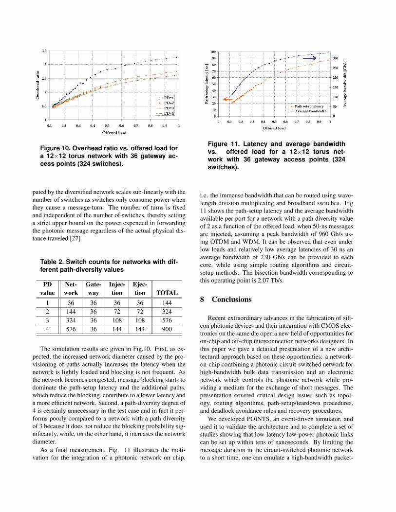
Figure 10. Overhead ratio vs. offered load fora 12×12 torus network with 36 gateway ac-cess points (324 switches).
pated by the diversified network scales sub-linearly with thenumber of switches as switches only consume power whenthey cause a message-turn. The number of turns is fixedand independent of the number of switches, thereby settinga strict upper bound on the power expended in forwardingthe photonic message regardless of the actual physical dis-tance traveled [27].
Table 2. Switch counts for networks with dif-ferent path-diversity values
PD Net- Gate- Injec- Ejec-value work way tion tion TOTAL
1 36 36 36 36 1442 144 36 72 72 3243 324 36 108 108 5764 576 36 144 144 900
The simulation results are given in Fig.10. First, as ex-pected, the increased network diameter caused by the pro-visioning of paths actually increases the latency when thenetwork is lightly loaded and blocking is not frequent. Asthe network becomes congested, message blocking starts todominate the path-setup latency and the additional paths,which reduce the blocking, contribute to a lower latency anda more efficient network. Second, a path-diversity degree of4 is certainly unnecessary in the test case and in fact it per-forms poorly compared to a network with a path diversityof 3 because it does not reduce the blocking probability sig-nificantly, while, on the other hand, it increases the networkdiameter.
As a final measurement, Fig. 11 illustrates the moti-vation for the integration of a photonic network on chip,
Figure 11. Latency and average bandwidthvs. offered load for a 12×12 torus net-work with 36 gateway access points (324switches).
i.e. the immense bandwidth that can be routed using wave-length division multiplexing and broadband switches. Fig11 shows the path-setup latency and the average bandwidthavailable per port for a network with a path diversity valueof 2 as a function of the offered load, when 50-ns messagesare injected, assuming a peak bandwidth of 960 Gb/s us-ing OTDM and WDM. It can be observed that even underlow loads and relatively low average latencies of 30 ns anaverage bandwidth of 230 Gb/s can be provided to eachcore, while using simple routing algorithms and circuit-setup methods. The bisection bandwidth corresponding tothis operating point is 2.07 Tb/s.
8 Conclusions
Recent extraordinary advances in the fabrication of sili-con photonic devices and their integration with CMOS elec-tronics on the same die open a new field of opportunities foron-chip and off-chip interconnection networks designers. Inthis paper we gave a detailed presentation of a new archi-tectural approach based on these opportunities: a network-on-chip combining a photonic circuit-switched network forhigh-bandwidth bulk data transmission and an electronicnetwork which controls the photonic network while pro-viding a medium for the exchange of short messages. Thepresentation covered critical design issues such as topol-ogy, routing algorithms, path-setup/teardown procedures,and deadlock avoidance rules and recovery procedures.
We developed POINTS, an event-driven simulator, andused it to validate the architecture and to complete a set ofstudies showing that low-latency low-power photonic linkscan be set up within tens of nanoseconds. By limiting themessage duration in the circuit-switched photonic networkto a short time, one can emulate a high-bandwidth packet-

switched network, with an average bandwidth on the orderof hundreds of Gb/s per core.
While the exchange of data at such bandwidths leads toexceedingly high power dissipation in electronic NoCs, in aphotonic NoC, end-to-end paths are formed across a chainof low-power transparent switching elements. Power con-sumed in routing the high-bandwidth messages can there-fore be dramatically reduced. Photonic NoCs can present atrue leap in the sheer performance of intrachip interconnec-tion networks and, more importantly, in their performanceper watt.
References
[1] L. Benini and G. D. Micheli. Networks on chip: A new SoCparadigm. IEEE Computer, 49(2/3):70–71, Jan. 2002.
[2] R. W. Brodersen, M. A. Horowitz, D. Markovic, B. Nikolic,and V. Stojanovic. Methods for true power minimization. InIntl. Conf. on Computer-Aided Design, pages 35–42, Nov.2002.
[3] L. P. Carloni and A. L. Sangiovanni-Vincentelli. Copingwith latency in SoC design. IEEE Micro, 22(5):24–35,Sept./Oct. 2002.
[4] X. Chen, B. G. Lee, X. Liu, B. A. Small, I.-W. Hsieh,K. Bergman, J. Richard M. Osgood, and Y. A. Vlasov.Demonstration of 300 Gbps error-free transmission ofWDM data stream in silicon nanowires. In Conference onLasers and Electro-Optics (CLEO’07), May 2007.
[5] W. J. Dally and C. L. Seitz. Deadlock-free message routingin multiprocessor interconnection networks. IEEE Trans.Comput., 36(5):547–553, May 1987.
[6] W. J. Dally and B. Towles. Route packets, not wires: On-chip interconnection networks. In Design Automation Conf.,pages 684–689, June 2001.
[7] W. J. Dally and B. Towles. Principles and Practices of In-terconnection Networks. Morgan Kaufmann, San Francisco,CA, 2004.
[8] C. Gunn. CMOS photonics for high-speed interconnects.IEEE Micro, 26(2):58–66, Mar./Apr. 2006.
[9] A. Gupta, S. P. Levitan, L. Selavo, and D. M. Chiarulli.High-speed optoelectronics receivers in SiGe. In 17th Intl.Conf. on VLSI Design, pages 957–960, Jan. 2004.
[10] A. Hemani, A. Jantsch, S. Kumar, A. Postula, J. Oberg,M. Millberg, and D. Lindqvist. Network on chip: An ar-chitecture for billion transistor era. In 18th IEEE NorChipConference, Nov. 2000.
[11] S. Heo and K. Asanovic. Replacing global wires with anon-chip network: a power analysis. In Intl. Symp. on LowPower Elect. and Design (ISLPED 2005), pages 369–374,Aug. 2005.
[12] R. Ho. Wire scaling and trends. a presentation at MTODARPA meeting, Aug. 2006.
[13] R. Ho, K. W. Mai, and M. A. Horowitz. The future of wires.Proc. IEEE, 89(4):490–504, Apr. 2001.
[14] M. A. Horowitz, E. Alon, D. Patil, S. Naffziger, R. Kumar,and K. Bernstein. Scaling, power, and the future of CMOS.In IEEE Intl. Electron Devices Meeting, Dec. 2005.
[15] I.-W. Hsieh, X. Chen, J. I. Dadap, N. C. Panoiu, J. RichardM. Osgood, S. J. McNab, and Y. A. Vlasov. Ultrafast-pulse self-phase modulation and third-order dispersion in siphotonic wire-waveguides. Optics Express, 14(25):12380–12387, Dec. 2006.
[16] L. A. Johansson, Z. Hu, D. J. Blumenthal, L. A. Coldren,Y. A. Akulova, and G. A. Fish. 40-GHz dual-mode-lockedwidely tunable sampled-grating DBR laser. IEEE Photon.Technol. Lett., 17(2):285–287, Feb. 2005.
[17] S. Kawanishi, H. Takara, K. Uchiyama, I. Shake, andK. Mori. 3 Tbit/s (160 Gbit/s×19 channel) optical TDMand WDM transmission experiment. Electronic Letters,35(10):826–827, 13 May 1999.
[18] M. Kistler, M. Perrone, and F. Petrini. Cell multiproces-sor communication network: Built for speed. IEEE Micro,26(3):10–23, May/June 2006.
[19] R. Kumar, V. Zyuban, and D. M. Tullsen. Interconnec-tions in multi-core architectures: Understanding mecha-nism, overheads, scaling. In ISCA ’05: 32nd annual inter-national symposium on Computer architecture, June 2005.
[20] B. G. Lee, B. A. Small, Q. Xu, M. Lipson, and K. Bergman.Demonstrated 4×4 Gbps silicon photonic integrated parallelelectronic to WDM interface. In Optical Fiber Communica-tions Conf. (OFC), Mar. 2007.
[21] L. Liao, D. Samara-Rubio, M. Morse, A. Liu, D. Hodge,D. Rubin, U. D. Keil, and T. Franck. High speed sili-con mach-zehnder modulator. Optics Express, 13(8):3129–3135, 18 Apr. 2005.
[22] T. Mudge. Power: A first-class architectural design con-straint. IEEE Computer, 34(4):52–58, 2001.
[23] OMNeT++ discrete event simulation system. available on-line at http://www.omnetpp.org/.
[24] T. M. Pinkston and J. Shin. Trends toward on-chip net-worked microsystems. Intl. J. High Performance Computingand Networking, 3(1):3–18, 2001.
[25] R. Ramaswami and K. N. Sivarajan. Optical Networks: APractical Perspective. Morgan Kaufmann, San Francisco,CA, second edition, 2002.
[26] A. Shacham and K. Bergman. Building ultra low latencyinterconnection networks using photonic integration. IEEEMicro, Mar./Apr. 2007. to be published.
[27] A. Shacham, K. Bergman, and L. P. Carloni. MaximizingGFLOPS-per-Watt: High-bandwidth, low power photonicon-chip networks. In P=ac2 Conference, pages 12–21, Oct.2006.
[28] F. Xia, L. Sekaric, and Y. A. Vlasov. Ultracompact opticalbuffers on a silicon chip. Nature Photonics, 1:65–71, Jan.2007.
[29] Q. Xu, S. Manipatruni, B. Schmidt, J. Shakya, and M. Lip-son. 12.5 Gbit/s carrier-injection-based silicon microringsilicon modulators. Optics Express, 15(2):430–436, 22 Jan.2007.
[30] Q. Xu, B. Schmidt, S. Pradhan, and M. Lipson. Micrometre-scale silicon electro-optic modulator. Nature, 435:325–327,19 May 2005.
[31] Q. Xu, B. Schmidt, J. Shakya, and M. Lipson. Cascaded sil-icon micro-ring modulators for WDM optical interconnec-tion. Optics Express, 14(20):9430–9435, 02 Oct. 2006.