optical and physical properties of solgel-derived geo_2:sio_2 films in photonic applications
TRANSCRIPT

Optical and physical properties of solgel-derivedGeO2:SiO2 films in photonic applications
Charles K. F. Ho,1 Rajni,1 H. S. Djie,1,2 Kantisara Pita,1 Nam Quoc Ngo,1,* and T. Osipowicz3
1Photonics Research Centre, School of Electrical and Electronic Engineering, Nanyang Technological University,50 Nanyang Avenue, Singapore 639798
2Department of Electrical and Computer Engineering, Lehigh University, Bethlehem, Pennsylvania, USA3Centre of Ion Beam Applications, Department of Physics, National University of Singapore, Singapore 117542
*Corresponding author: [email protected]
Received 7 December 2006; accepted 13 February 2007;posted 7 March 2007 (Doc. ID 77735); published 20 June 2007
The functionality of optical components relies heavily on the composition-dependent properties of ger-manosilicate materials, which include the refractive index, photosensitivity, and microstructural prop-erties. Recent studies and parallel developments are presented of germanosilicate films with compositionx of Ge content (i.e., xGeO2:�1 � x�SiO2) that were synthesized by the solgel process for various integratedphotonic applications undertaken. The following novel aspects are discussed with respect to the effect ofcomposition of the glassy films �0.05 � x � 0.40�: determination of spectral optical properties, UVimprinting of optical waveguides with relatively large index change ��n�, and quantum-well intermixingenhancement observed in InGaAs�P��InP quantum-well optical devices. The implications of the resultsare discussed. © 2007 Optical Society of America
OCIS codes: 160.6060, 130.3130, 130.0250, 130.5990, 310.6860, 230.5590.
1. Introduction
Ever since the deployment of optical fibers in the1980s, the germanosilicate glass has been the materialof choice for many devices operating within the tele-communication window. Soon after, photosensitivityin such glass was discovered, enabling the fabricationof devices such as fiber gratings, waveguide gratings,and recently the direct writing of optical devices [1,2].Besides the ability to change the refractive index (RI)by either varying the composition of the germanosili-cate or the dosage of UV exposure, the change in phys-ical properties and microstructure can be exploited insome photonic applications. In this paper, we presentour work on three aspects of germanosilicate films:spectral properties (viz., optical dispersion), UV pho-tosensitivity leading to UV imprinting of opticalwaveguides, and porous germanosilicate films as anencapsulant layer for quantum-well intermixing (QWI).
With a higher electronic polarizability in GeO2, itsaddition into a SiO2 matrix is to raise the RI to
achieve index guiding of near-infrared lightwaves.The relatively high RI of the core region affords stron-ger optical confinement, hence, reducing bend lossand device size [3–5]. Despite the number of priorstudies of GeO2:SiO2 films [6–9] reports to date lackthe spectroscopic details about the RI, which arevaluable in the light of the foreseeable expansion inthe telecommunication window (in the range of �1.2to 1.7 �m). Advances in metrology have enabled pre-cise determinations of the optical constants of filmsby spectroscopic ellipsometry ��10�3� [10]. Compre-hensive characterization has been performed on theprecise physical microstructure of the film samples,which allows an accurate determination of the dis-persion (i.e., the spectral change of RI with wave-length) for different compositions [11]. The Sellmeierdispersion model was effectively used to describe theoptical dispersion properties of the GeO2:SiO2 filmsfor a range of wavelengths from 210 to 1700 nm.
The UV-induced RI change (photosensitivity) of thecore layer presents an alternative technique with twoattractive advantages in the fabrication of opticalwaveguide based devices. First, waveguiding devices
0003-6935/07/204397-10$15.00/0© 2007 Optical Society of America
10 July 2007 � Vol. 46, No. 20 � APPLIED OPTICS 4397

can be defined without the need to do lithography andetching where sidewall roughness adversely affectsthe performance of the waveguides. Secondly, post-fabrication adjustments of complex devices are pos-sible to remedy for fabrication imperfections [12–15].For large-scale device integration, one desirable at-tribute of direct-writing techniques is to achieve highpermanent RI change (cf. RI contrast). Photosensitiv-ity, in this context, refers to the photo-induced chem-ical modification of the inorganic glass, which resultsin a change in the RI, �n. Although the exact mech-anisms that cause such change in the RI are still thesubject of debates at presence, many studies haveshown that such photosensitivity is, in fact, associ-ated with nonstoichiometric defects [16–20], whichincrease with the concentration of germanium [21–23]. Photosensitivity in optical fibers and, hence, fiberBragg gratings have traditionally been restricted tovalues of �n � 10�4 [24,25]. On the other hand, pla-nar optical waveguides provide a platform that has asubstantially higher level of flexibility in terms ofcomposition of the core. Recent works have reportedachievements in the range of �n � 10�3 [24,26] fab-ricated by deposition methods such as vapour axialdeposition and chemical vapor deposition (CVD) withadditional UV-sensitization processes of hydrogenand thermal treatments. Recently, we demonstratedthat an increase in RI up to 0.0098 has been achievedwhen our solgel derived germanosilicate films of ap-proximately �200 nm in thickness were exposed toUV light. Such an increase in RI was attributed to thecreation of an oxygen deficient center without em-ploying any sensitization technique [27].
In another application dealing with photonic inte-gration, we exploited the composition-dependent mi-crostructural properties of the germanosilicate films.The technique of QWI [28] allows reliable and low-cost modifications of QW bandgap energy on the as-grown wafer. QWI has been found to be a moremanufacturing-friendly process over the traditionalgrowth–regrowth and selective-area growth processto achieve photonic integration because of its abilityto selectively fine-tune the QW bandgap in differentregions within the same epitaxial layer structure,through the interdiffusion between the QW and theadjacent barrier material [28,29]. The mechanismsthat afford QWI involve the creation of disordering inthe top barrier layer and subsequently the thermallyactivated interlayer diffusion of the created defectsand constituents of the QW layers (i.e., Group III andV ions) leading to a change in the energy profileacross the QW. Certainly, the QWs can tolerate onlya suitable annealing temperature to promote the in-termixing while retaining the crystalline quality. Ahigh annealing temperature may cause the severesurface out-diffusion and dopant redistribution, whichmay contribute to the significant intrinsic waveguideloss due to free carrier absorption [29]. Compared withalternative techniques (e.g., laser-induced disordering,plasma-induced disordering, and impurity-induceddisordering) [28] dielectric cap-induced disordering
can be seen to be commercially attractive in large-scaleproduction as it involves the deposition of a dielectriclayer, which can be applied to large areas. In addition,device integration can be implemented economicallyby simple schemes involving area-selective bandgapmodification [30,31]. The key to this process is theability to tailor the dielectric properties to spatiallycontrol the interdiffusion rate in the QW. Hence thesolgel process is expected to provide added values as alow-cost alternative of QWI techniques. While priorreports have shown the enhancement of QWI by theuse of silica-based solgel caps on GaAs-based QWswith a very restrictive amount of doping of phorpho-rous [32,33] ��5 mol. %�, our results [34] distinctlydemonstrate the modification of excitonic emission inInP-based QWs using a highly doped solgel-silica cap.We discuss the effect of germanosilicate encapsulantlayer (i.e., the dielectric cap) on the trimming of thebandgap energy of InGaAs(P)�InP QW laser struc-ture.
2. Experimental Procedures
The raw materials of the solgel process incorporateprecursors (tetraethoxysilane, 98% and germaniumisopropoxide, 99.99%), which are readily soluble incommon solvents. The details of the process are de-scribed in Fig. 1. Tetraethoxysilane (TEOS) was pre-hydrolyzed in a mixture (Sol-S) of ethanol and acidified(HCl) water of pH 1; the molar ratio of each componentin the respective order was 1:4:2. Ge isopropoxide wasdiluted in anhydrous isopropanol at a molar ratio of 1:4in a stock solution (Sol-G) in a N2-purged glovebox(relative humidity �30%). An appropriate volumewas later extracted from Sol-G and added to the Sol-Sto become the Sol-SG for a desired composition ofxGeO2:�1 � x�SiO2 for 0.05 � x � 0.40. After a periodof ageing ��1–4 h� under rigorous mechanical agita-tion, the Sol-SG, was then spin coated on the desiredsubstrate (silicon or III-V) depending on the intendedapplications. The dilution step was only used asneeded to ensure that the solution remain clear dur-ing the ageing period. This spin-coating process wasperformed in a N2-purged glovebox. The dried gelfilms were typically subjected to thermal treatmentby a rapid thermal processor (RTP) for annealingperiods for 20 s with a ramp rate of �25 °C�s or by anelectric furnace with air ambient for annealing peri-ods �10 min at temperature �1000 °C.
A. Thin Films for the Determination of the SpectralProperties
In the study of spectro-optical properties, thin films(thickness of �200 nm) of single coating were depos-ited at 1000 rpm on Si (100) substrates. The filmswere annealed in an electric furnace for 10 to 15 minat temperatures of 1000 °C to 1100 °C. The fabrica-tion of planar waveguides followed closely the methodproposed by Syms et al. [35,36]. Each coating wasdeposited at �2000 rpm. The dispersion properties ofgermanosilicate films were determined by the use ofa variable angle spectroscopic ellipsometry (VASE)from J. A. Woollam, in a reflection mode at 60° and
4398 APPLIED OPTICS � Vol. 46, No. 20 � 10 July 2007

75° angles of incidence. The WVASE2.0 software wasused to analyze the data from 210 to 1700 nm. Thedetails of the measurements can be found in an ear-lier publication [11].
B. Ultraviolet-Imprinted Channel Waveguides
Multiple cycles of spin coating were required toachieve a suitable thickness of �3 �m at a composi-tion of x � 0.20 on a Si wafer with 10 �m thermaloxide. The RTP was used to anneal the sample at900 °C in flowing O2 gas after every coating cycle. Aconsolidation step was carried out in the electric fur-nace at 1000 °C for over 30 min. To form channelwaveguides and devices by direct UV writing tech-nique, the solgel-derived core germanosilicate layerwas radiated using a KrF excimer laser �248 nm� for�10 min at 450 mJ�pulse (beam size 24 � 12 mm2)and 10 Hz. The required RI contrast was realized bythe use of a photomask in contact with the surface ofthe sample. Channel waveguides were characterizedby taking a near-field image of the optical output bylaunching 1.55 �m lightwaves via a single-mode fiber(SMF) in a butt-couple configuration. The image wasviewed with a 40� objective lens and recorded by aCCD camera using the BEAMProfile analysis soft-ware.
C. Solgel-Derived Encapsulant-Induced Quantum-WellIntermixing
The encapsulant porous GeO2:SiO2 was spin coatedat 2500 rpm on substrates that contained the QWs.The lattice-matched InGaAs�InGaAsP QW laserstructure was grown by metalorganic vapor phase
epitaxy on (100)-oriented InP substrates as reportedearlier [37]. The active region consists of five periodsof 55 Å In0.53Ga0.47As QWs with 120 Å InGaAsP bar-riers. Prior to the annealing using a RTP in flowingN2 ambient for 2 min, the solgel capped samples wereprebaked on a hot plate at 160 °C for 5 min to evap-orate the residual solvent. QWI was activated by anannealing step at 630 °C for 2 min under flowing N2gas with a GaAs proximity cap. Photoluminescence(PL) at 77 K was performed on the QW samples toassess the degree of bandgap shift and linewidthbroadening (viz., the extent of QWI) using an Nd:YAGlaser �1.064 �m� as an excitation source.
3. Results and Discussions
A. Spectral Properties of Germanosilicate Films
To ensure an accurate reproduction of the opticalconstants from spectroscopic ellipsometry (SE) anal-ysis, a rigorous characterization of the physicalstructure of the samples after annealing has beenperformed. In brief, the IR absorption spectra showeda high degree of random mixing between the germa-nium and silicon oxides and low OH content, andRutherford backscattering (RBS) measurements re-vealed stoichiometric (i.e., O��Ge � Si� 2) binaryoxide films were achieved [Fig. 2(a)]. Using theRUMP simulation, the areal atomic density of thefilm was determined from the RBS spectra. Combin-ing with the thickness derived from the SE data, thedensity of the films was found. In Fig. 2(b) the densityof the samples is in good agreement with the linearapproximation calculated from the density of pure
Fig. 1. Process flow of the fabrication of thick films involved in this work. The synthesis of porous or dense single-layer thin filmessentially follows the same chemical mixing and spin coating procedures.
10 July 2007 � Vol. 46, No. 20 � APPLIED OPTICS 4399

SiO2 and GeO2 (i.e., 2.202 and 3.604 g�cm3, respec-tively [7]) and the density values as determined byHuang et al. [7]. In an attempt to reduce the noise ofthe measurement data and to avoid possible correla-tion between the parameters of the dispersion modeland others involved in the SE analysis, a multi-sample and multiangle measurement strategy wasadopted [11,38,39] for a spectral range of 210–1700 nm.
Assuming negligible absorption (as validated byUV-VIS spectra down to 190 nm), the Sellmeier dis-persion formula [38] was used to model the dispersionof the germanosilicate films. The Sellmeier disper-sion formula is expressed as
n2 0 �a�2
�2 � b2 � c�2, (1)
where 0, a, b, c are the adjustable characteristicSellmeier parameters. The SE model incorporatingthe Sellmeier dispersion formula shows good fits(mean-square error below 3) to the measured SEdata. The resulting composition-dependent RI isclearly demonstrated in Fig. 2. Such a linear trend istypical of many silica-based materials [40], and theincrease in RI with x as a result of an increase inpolarizability and density can be explained by theLorentz–Lorenz relationship [7,41]. A comparisonwith results from prior works at selected wavelengthsillustrates the fidelity of the Sellmeier dispersionand that the density of the germanosilicate films fab-ricated using our solgel process is comparable toglasses formed by CVD [Bellman et al. [9], RI at1550 nm, n(NIR)]. The Sellmeier dispersion relationsrepresenting the measured compositions are plottedin Fig. 3. The linear variation of RI with composition
(x) noted in Fig. 2(c) allows an interpolation of thedispersion relationships forming a 3D data plot [11].These data sets can then be used to predict values(either composition or RI) at a given wavelength.
In optical communications, the material dispersioncoefficient, DMAT, is defined as
DMAT ��
c�2n
��2, (2)
where c refers to the speed of light in vacuum. TheSellmeier dispersion relationships determined from
Fig. 2. (a) Stoichiometry of solgel synthesized xGeO2:�1 � x�SiO2 films determined by RBS. (b) Density of the films calculated using theareal atomic density from RBS and the thickness deduced from the SE analysis. (c) Linearity of the variation in RIs with composition. Thedashed line represents the linear regression of the n(He–Ne) data from this work. RIs for the various important wavelengths are shown(see text).
Fig. 3. Sellmeier dispersion for the selected compositions, 0 � x� 0.4. Inset shows the zero-dispersion wavelengths for the differ-ent compositions.
4400 APPLIED OPTICS � Vol. 46, No. 20 � 10 July 2007

the SE analysis can be used to calculate DMAT for eachcomposition (x) by substituting Eq. (1) into Eq. (2).Setting DMAT 0, the zero-dispersion wavelength isshown to increase with x (inset of Fig. 3). We thenconclude that the material dispersion is sensitive tothe Ge content within the optical communicationwindow, and the zero-dispersion wavelength can betailored by selecting a specific x value.
B. Photosensitivity and Direct Writing of OpticalWaveguides
Although laser-written waveguides in SiO2 havebeen reported [42], the incorporation of GeO2 willenhance the achievable increase in the change ofan UV-induced RI, �n [23]. A �n of 2.3 � 10�3 wasachieved in a planar waveguide (core-layer thicknessof �3 �m) with low loss �0.5 dB�cm as character-ized by the prism-coupled configuration [27]. Asingle-mode optical signal can be seen quite clearlyfrom the figure for a 6 mm long channel waveguideFig. 4(a).
The effectiveness of the optical guiding ability can beseen through the intensity profiles of the near-fieldimage. The measured profiles along the X and Y axesare shown respectively as X expt and Y expt in Fig.4(b). A profile of a Gaussian approximation of the fun-damental mode, using the value of �n as measured bythe prism coupler, is presented (X Gmode) as a com-parison. The asymmetry of the Y expt profile can beunderstood from the inherent air-GeO:SiO2-SiO2structure. The slight asymmetry of the X expt curvecould possibly be attributable to the imperfections inthe UV irradiation setup leading to nonuniform irra-diance and�or nonpolished end face of the waveguide,causing wavefront distortion at the waveguide out-put. Without guiding (i.e., planar waveguide withoutUV exposure), the lightwaves launched from theSMF after a propagation length of 500 �m in thewaveguide would experience diffraction, causing
broadening of the beam profile as shown by X Gdiff inFig. 4(c) along the X axis. The theoretical intensityprofiles were calculated according to expressionsgiven in a prior report [43]. From the comparison ofX expt, X Gmode, and X Gdiff, the achieved �n andeffectiveness of the direct-writing technique can beascertained. This is made possible owing to the abil-ity to induce relatively high �n by the UV radiation toconfine the lightwaves. In most cases, the values of�n are relatively small, of the order of 10�5–10�4
[44,45], which are inadequate for strong confinementof the lightwaves. The change in refractive index isnormally explained in terms of a number of photo-chemical reactions involving oxygen-deficient defectssuch as the neutral oxygen monovacancy (NOMV)and Ge2� [44,45]. The defects are shown schemati-cally in Fig. 5.
Sakoh et al. [26] reported a RI change of approxi-mately 10�3 involving highly photosensitive Ge2� cen-ters [(Fig. 5(c)]. Our work has shown that �n of ashigh as 9.8 � 10�3 for films of thickness �200 nm canbe achieved by the combination of UV radiation andthe solgel spin-coating process, yielding pure inor-ganic films [27]. This relatively high value of �n isexplained in terms of the creation of oxygen relateddefects [27].
C. Quantum-Well Intermixing Using GermanosilicateEncapsulant Layer
The annealed bare sample of an incomplete laserstructure used in this study, shown in Fig. 6(a), ex-hibits only a small bandgap blueshift of �12 nm. Theincomplete structure refers to the full laser structureafter subsequent removal of highly doped InGaAscontact layers above the QW region. Figure 6(a) alsoshows that a change in the PL peak wavelength isaffected by the compositions of the germanosilicatecap layer. Evidently, the solgel cap enhances the in-termixing rate in QWs. At Ge content of x � 0.1, the
Fig. 4. (a) Near-field image of the optical output of a direct-written channel waveguide. Aperture of the mask is 5 �m. (b) Normalizedintensity profiles of the measured beam profile across the X axis (X expt) and Y axis (Y expt); the theoretical profile derived from theGaussian field approximation (X-Gmode); the abscissa is in units of micrometers. (c) Comparison between the Gaussian approximation ofintensity profile with guiding (X Gmode) and without guiding (X Gdiff) in X.
10 July 2007 � Vol. 46, No. 20 � APPLIED OPTICS 4401
PL peak shift remains constant at �16 nm. Beyondthis there is nearly a linear increase in the PL shiftup to x � 0.30.
We further perform the intermixing study on thecomplete QW laser structure to demonstrate the post-growth bandgap tuning using the solgel cap. Bare(uncapped) samples and samples capped by e-beam-evaporated SiO2 (EBSi) were also annealed for com-parison. In Fig. 6(b), we obtain four distinguished PLspectra from bare samples and capped samples withthe EBSi and Ge-doped solgels (x 0.00 and 0.16).The PL peaks for EBSi, uncapped, x 0 and 0.16 arerespectively 1456, 1436, 1408, and 1392 nm. This re-sult highlights the spatial bandgap selectivity using acombination of dielectric caps. The control sample
and the intermixed sample �x 0.16� exhibit a com-parable PL linewidth ��40 meV� while the as-grownPL has a linewidth of 44 meV. The negligibly smalllinewidth broadening infers the retention of the op-tical quality after intermixing. The overall blueshiftsin the complete laser structure are enhanced whencompared to the incomplete structure. The presenceof Ga atoms from the InGaAs contact layer below thesolgel cap is responsible for the increase in the degreeof intermixing from the complete laser structure.
It has been known that porosity and thermal ex-pansion of the cap are two important parameters forthe dielectric layer in dielectric cap-induced disorder-ing [33]. From the curves of (iii) and (iv), the solgelcaps exhibit an enhancement in the degree of inter-
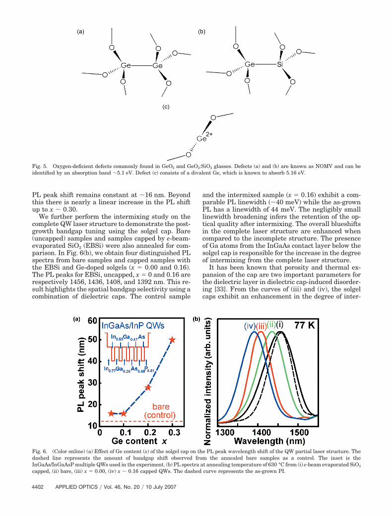
Fig. 5. Oxygen-deficient defects commonly found in GeO2 and GeO2:SiO2 glasses. Defects (a) and (b) are known as NOMV and can beidentified by an absorption band �5.1 eV. Defect (c) consists of a divalent Ge, which is known to absorb 5.16 eV.
Fig. 6. (Color online) (a) Effect of Ge content (x) of the solgel cap on the PL peak wavelength shift of the QW partial laser structure. Thedashed line represents the amount of bandgap shift observed from the annealed bare samples as a control. The inset is theInGaAs/InGaAsP multiple QWs used in the experiment. (b) PL spectra at annealing temperature of 630 °C from (i) e-beam evaporated SiO2
capped, (ii) bare, (iii) x 0.00, (iv) x � 0.16 capped QWs. The dashed curve represents the as-grown PI.
4402 APPLIED OPTICS � Vol. 46, No. 20 � 10 July 2007

mixing when compared to the EBSi film due to theporous nature as observed earlier in our FTIR andellipsometry results [46]. Figure 7 summarizes therelationship of porosity and the Ge content in thesolgel films with the annealing treatments. The in-corporation of Ge into the films gives a reduction inthe porosity of films. This contradicts the intermixingenhancement results in the x � 0.16 caps if the po-rosity is the dominant effect in the solgel cap-inducedintermixing. We identify that there is a substantialincrease in the thermal expansion with the additionof Ge into the films [7]. Compressive stress is knownto favor the transformation of vacancy defects intoantisites [33,47], hence the degree of intermixing isreduced. Such compressive stress in the semiconduc-
tor QWs exists because of the large difference in thecoefficients of the semiconductor material ��10�6�and the solgel glass ��10�7�. Considering the magni-tude of change in the cap porosity and the thermalexpansion as a result of the increase in Ge content, anestimate can be obtained from the above references tobe ��4.4% � 6.8%��6.8% � 100� � �35.3% (see Fig. 7)and ��2.4 � 0.5��0.5 � 100� � 380% [7], respectively.Although the relative effect of the above two param-eters for the current material system is not known,the change in the thermal expansion is likely to bethe dominating factor that enables the control of theQWI via vacancy diffusion by the addition of Ge.
To further substantiate the vacancy outdiffusionrole in the QWI enhancement at various Ge content,we carried out a similar intermixing process to theGaAs�AlGaAs multiwidth QWs structure. The struc-ture was chosen for two main reasons. First, the in-termixing in this structure is solely governed by thegroup III atomic interdiffusion from the effective Gavacancy injection. Second, the structure permits thedepth-resolved intermixing degree by measuring thechange in the individual PL peak after intermixing[48]. We compare the GaAs�AlGaAs QW intermixingwith x 0.10 and x 0.40 at relatively low annealingtemperatures for GaAs-based QWI in Fig. 8. Notethat the typical QWI process temperature for theGaAs�AlGaAs system is above 850 °C. At this an-nealing condition, there is no effect on the thermalshift under control samples. Figure 8(a) shows theinsignificant QWI effect in the x � 0.1 cap at RTA of650 °C, which is similar to the previous case in theInGaAsP QWs. In ths case of x � 0.4 cap, the QWIeffect is greatly pronounced, and the PL spectra hasbeen blueshifted for all four QWs. The signal corre-sponding to the narrowest well, QWI, is not clearlyresolved after annealing, implying that the well has
Fig. 7. Porosity–Ge map demonstrating both the effect of anneal-ing temperature and Ge content on the film porosity; dashed linesrepresent a fit-by-eye guide for the data points at each annealingtemperature [47].
Fig. 8. (Color online) Photoluminescence at 77 K from (i) as-grown, (ii) control (annealed bare), and (iii) solgel capped samples: with (a)x 0.1 and (b) x 0.40 to the intermixing in the GaAs�Al0.2Ga0.8As multiwidth QWs (QW1, 3 nm; QW2, 5 nm; QW3, 6 nm; andQW4, 8 nm). The annealing was performed at 650 °C for 2 min.
10 July 2007 � Vol. 46, No. 20 � APPLIED OPTICS 4403

been totally intermixed or dissolved to the surround-ing AlGaAs barrier. The result further validates therole of efficient creation of beneficial vacancies viastress relaxation in the Ge-added solgel that leads tothe pronounced degree of intermixing.
The activation energy and diffusion coefficient cor-respond to the energy associated with the motion andformation of defects during the dielectric cap anneal-ing process. The annealing temperature-dependentbandgap shift can be used to deduce the diffusioncoefficients (assumed to be independent of defectconcentration), DQW, and to extract the activation en-ergy, EA [49]. Figure 9(a) summarizes the relation-ship of annealing temperature and bandgap shift forcaps of x 0.00 and 0.16 from the InGaAs-InP QWsusing Ge-dopant. For completion, we also include theexperimental data of solgel cap-induced intermixingon GaAs substrate by Lee et al. [50]. As shown inFigure 9(b), the experimental data are linearly fittedover 1000�T to the Arrhenius equation DQW � exp��EA�kT�, where T and EA refer to the annealing tem-perature and the activation energy, respectively. Thisyields the extracted EA 1.7 0.5 eV for both cases,which is significantly lower than the common InP-based and GaAs-based QWI processes [51,52]. Nearlyidentical EA intuitively implies that the discrepancyin interdiffusion behavior between x � 0.16 andx 0.00 is only attributed to the difference in thenumber of beneficial vacancies that involve in theQWI, which is in good agreement with the experi-mental data of the GaAs�AlGaAs QW intermixingearlier. This result further corroborates postulationthat the compressive stress reduces the effective va-cancy responsible for intermixing enhancement inthe Ge-added film. Therefore the enhancement ofQWI by the increased doping of the Ge content can beascribed to the large magnitude of change in the ther-
mal expansion leading to the retention of vacanciesthat drives QWI.
Understanding that stress, rather than porosity,has a dominant affect in the QWI in the abovescheme, some inferences can be made about the se-lection of the suitable process that takes advantage ofthe QWI control using the GeO2:SiO2 solgel caps inimplementing spatial-selective QWI on semiconduc-tor platforms. Pepin et al. [31] and Deenapanray et al.[53] have shown that by depositing a Si3N4 layer atopof a patterned or nonpatterned encapsulant SiO2layer, QWI was univocally suppressed while a singlelayer SiO2 typically enhances QWI. This unexpectedobservation was attributed to the fact that the near-surface stress distribution in the semiconductor wasdrastically modified (i.e., reversed). Therefore theQWI performance of spatial areas, which are under-neath any multiple layer of varying GeO2:SiO2 solgelfilms may deviate from the results found in thepresent work. On the contrary, if the cap porosity wasthe more dominant factor in the QWI process, thenthe above stress-induced QWI deviation is unlikely tooccur. As a foresight, there are a number of low-costprocesses that are well suited to implement the aboveQWI scheme. Such process as printing, which in-volves the simultaneous deposition of multiple solu-tions, may open up new opportunities for low-costphotonic integration.
4. Conclusion
Optical constants have been modeled by the Sellmeierdispersion for films with compositions of x � 0.400over a broad spectral range of 210 to 1700 nm. TheRI-composition-wavelength 3D dataset enables self-consistent prediction of values with two known pa-rameter values. Further work is ongoing in anattempt to parameterize the Sellmeier values with
Fig. 9. (Color online) (a) PL peak wavelength shift versus the annealing temperature of an InGaAs�InP QW laser structure. (b) Diffusioncoefficient of QW �DQW� deduced from the experimental data as a function of the inversed annealing temperature for doped and undopedsolgel caps in our present work (InP substrate) and Lee et al. [51] (GaAs substrate). A representative best linear fit is shown for both datasets, whose slopes correspond to the activation energy.
4404 APPLIED OPTICS � Vol. 46, No. 20 � 10 July 2007

the composition of the germanosilicate films. Theo-retically, pure GeO2 is a better candidate than ger-manosilicate for the various applications in planarlightwave circuits and direct writing. However, ger-manosilicate �x � 0.600� or GeO2 is known to behygroscopic, and special chemical treatment is re-quired for handling the solgel chemistry with a highcontent of germanium precursors. Thus work involv-ing germanosilicate of x � 0.40 is beyond the scope ofthis article. Motivated by the possibility of the UVimprinting of waveguide devices (with appreciable RIcontrast, �n) and the commercial attractiveness ofthe solgel process, work has been done to improve thequality (uniformity and spin-coating artifacts) of ger-manosilicate films in the view of complex large-areadevices and large-scale integration. Results will bereported elsewhere. Besides the low-cost aspects ofthe solgel process, the unique and adjustable proper-ties of solgel derived films of germanosilicate glass(viz., porosity and thermal expansion) afford tunabil-ity of the bandgap energy in QW structures via QWIfor III–V platforms (such as InGaAs(P)�InP) thathave inherently low thermal stability.
This work was funded in part by the Agency forScience, Technology and Research (A*STAR) in Sin-gapore under the Optical Networking Focused Inter-ests Group (ONFIG) project. C. K. F. Ho and Rajniacknowledge the Research Scholarship provided byNanyang Technological University.
References1. K. O. Hill and G. Meltz, “Fiber Bragg grating technology fun-
damentals and overview,” J. Lightwave Technol. 15, 1263–1276 (1997).
2. Rajni, K. Pita, S. F. Yu, S. C. Tjin, and C. H. Kam, “Fabricationof inorganic GeO2:SiO2 channel waveguides by ultraviolet im-printing technique,” Appl. Phys. Lett. 89, 071105 (2006).
3. R. R. A. Syms and J. R. Cozens, Optical Guided Waves andDevices (McGraw-Hill, 1992).
4. F. Ladouceur and J. D. Love, Silica-Based Buried ChannelWaveguides and Devices, Optical and Quantum ElectronicsSeries (Chapman & Hall, 1996).
5. C. R. Pollock and M. Lipson, Integrated Photonics (KluwerAcademic, 2003).
6. K. Susa, I. Matsuyama, S. Satoh, and T. Suganuma, “Sol-gelderived Ge-doped silica glass for optical fiber application. I.Preparation of gel and glass and their characterization,” J.Non-Cryst. Solids 119, 21–28 (1990).
7. Y. Y. Huang, A. Sarkar, and P. C. Schultz, “Relationship be-tween composition, density and refractive index for germaniasilica glasses,” J. Non-Cryst. Solids 27, 29–37 (1978).
8. D.-G. Chen, B. G. Potter, and J. H. Simmons, “GeO2-SiO2 thinfilms for planar waveguide applications,” J. Non-Cryst. Solids178, 135–147 (1994).
9. R. A. Bellman, G. Bourdon, G. Alibert, A. Beguin, E. Guiot,L. B. Simpson, P. Lehuede, L. Guiziou, and E. LeGuen,“Ultralow loss high delta silica germania planar waveguides,”J. Electrochem. Soc. 151, G541–G547 (2004).
10. A. B. Djurisic, Y. Chan, and E. H. Li, “Progress in the room-temperature optical functions of semiconductors,” Mater. Sci.Eng., R. 38, 237–293 (2002).
11. C. K. F. Ho, K. Pita, N. Q. Ngo, and C. H. Kam, “Opticalfunctions of (x)GeO2:(1 � x)SiO2 films determined by multi-
sample and multiangle spectroscopic ellipsometry,” Opt. Ex-press 13, 1049–1054 (2005).
12. M. Abe, K. Takada, T. Tanaka, M. Itoh, T. Kitoh, and Y.Hibino, “Reduction in dispersion of silica-based AWG usingphotosensitive phase trimming technique,” Electron. Lett. 38,1673–1675 (2002).
13. J. Gehler and F. Knappe, “Crosstalk reduction of arrayedwaveguide gratings by UV trimming of individual waveguideswithout H2-loading,” in Optical Fiber Communication Confer-ence, Vol. 37 of OSA Trends in Optics and Photonics Series(Optical Society of America, 2000), paper WM9.
14. K. Takada and M. Abe, “UV trimming of AWG devices,” inBragg Gratings Photosensitivity and Poling in Glass Wave-guides, Vol. 93 in OSA Trends in Optics and Photonics Series(Optical Society of America, 2003), pp. 175–177.
15. D. A. Zauner, J. Hubner, K. J. Malone, and M. Kristensen, “UVtrimming of arrayed-waveguide grating wavelength divisiondemultiplexers,” Electron. Lett. 34, 780–781 (1998).
16. Q. Y. Zhang, K. Pita, C. K. F. Ho, N. Q. Ngo, L. P. Zuo, and S.Takahashi, “Low optical loss germanosilicate planar wave-guides by low-pressure inductively coupled plasma-enhancedchemical vapor deposition,” Chem. Phys. Lett. 368, 183–188(2003).
17. M. Takahashi, A. Sakoh, Y. Tokuda, T. Yoko, J. Nishii,H. Nishiyama, and I. Miyamoto, “Photochemical process ofdivalent germanium responsible for photorefractive indexchange in GeO2-SiO2 glasses,” J. Non-Cryst. Solids 345–346,323–327 (2004).
18. M. Takahashi, K. Ichii, Y. Tokuda, T. Uchino, T. Yoko, J.Nishii, and T. Fujiwara, “Photochemical reaction of divalent-germanium center in germanosilicate glasses under intensenear-ultraviolet laser excitation: Origin of 5.7 eV band and siteselective excitation of divalent-germanium center,” J. Appl.Phys. 92, 3442–3446 (2002).
19. J. Nishii, “Permanent index changes in Ge-SiO2 glasses byexcimer laser irradiation,” Mater. Sci. Eng. B 54, 1–10 (1998).
20. S. Agnello, R. Boscaino, F. La Mattina, S. Grandi, and A.Magistris, “Hydrogen-related paramagnetic centers in Ge-doped sol-gel silica induced by �-ray irradiation,” J. Sol-GelSci. Technol. 37, 63–68 (2006).
21. J. Nishii, H. Yamanaka, H. Hosono, and H. Kawazoe, “Char-acteristics of 5-eV absorption band in sputter deposited GeO2-SiO2 thin glass films,” Appl. Phys. Lett. 64, 282–284 (1994).
22. H. Hosono, Y. Abe, D. L. Kinser, R. A. Weeks, K. Muta, and H.Kawazoe, “Nature and origin of the 5-eV band in GeO2:SiO2
glasses,” Phys. Rev. B 46, 11445–11451 (1992).23. K. D. Simmons, G. I. Stegeman, B. G. Potter, Jr., and J. H.
Simmons, “Photosensitivity in germano-silicate sol-gel thinfilms,” J. Non-Cryst. Solids 179, 254–259 (1994).
24. M. Fokine and W. Margulis, “Large increase in photosensitiv-ity through massive hydroxyl formation,” Opt. Lett. 25, 302–304 (2000).
25. M. G. Sceats, G. R. Atkins, and S. B. Poole, “Photolytic indexchanges in optical fibers,” Annu. Rev. Mater. Sci. 23, 381–410(1993).
26. A. Sakoh, M. Takahashi, T. Yoko, J. Nishii, H. Nishiyama, andI. Miyamoto, “Photochemical process of divalent germaniumresponsible for photorefractive index change in GeO2-SiO2
glasses,” Opt. Express 11, 2679–2688 (2003).27. Rajni, K. Pita, S. C. Tjin, S. F. Yu, and C. H. Kam, “Enhanced
photosensitivity in sol-gel derived 20GeO2:80SiO2 thin films,”Appl. Phys. A 82, 535–541 (2006).
28. J. H. Marsh, “Quantum well intermixing,” Semicond. Sci.Technol. 8, 1136–1155 (1993).
29. E. H. Li, ed., Semiconductor Quantum Wells Intermixing, Op-toelectronic Properties of Semiconductors and Superlattices,Vol. 8 (Gordon & Breach, 2000), p. 695.
30. A. M. Kan’an, P. LiKamWa, Mitra-Dutta, and J. Pamulapati,
10 July 2007 � Vol. 46, No. 20 � APPLIED OPTICS 4405

“Area-selective disordering of multiple quantum well struc-tures and its applications to all-optical devices,” J. Appl. Phys.80, 3179–3183 (1996).
31. A. Pepin, C. Vieu, M. Schneider, H. Launois, and Y. Nissim,“Evidence of stress dependence in SiO2�Si3N4 encapsulation-based layer disordering of GaAs�AlGaAs quantum well het-erostructures,” J. Vac. Sci. Technol. B 15, 142–153 (1997).
32. P. Cusumano, B. S. Ooi, A. S. Helmy, S. G. Ayling, A. C. Bryce,J. H. Marsh, B. Voegele, and M. J. Rose, “Suppression of quan-tum well intermixing in GaAs�AlGaAs laser structures usingphosphorus-doped SiO2 encapsulant layer,” J. Appl. Phys. 81,2445–2447 (1997).
33. P. N. K. Deenapanray, B. Gong, R. N. Lamb, A. Martin, L. Fu,H. H. Tan, and C. Jagadish, “Impurity-free disordering mech-anisms in GaAs-based structures using doped spin-on silicalayers,” Appl. Phys. Lett. 80, 4351–4353 (2002).
34. H. S. Djie, C. K. F. Ho, T. Mei, and B. S. Ooi, “Quantum wellintermixing enhancement using Ge-doped sol-gel derived SiO2
encapsulant layer in InGaAs�InP laser structure,” Appl. Phys.Lett. 86, 081106 (2005).
35. R. R. A. Syms, “Stress in thick sol-gel phosphosilicate glassfilms formed on Si substrates,” J. Non-Cryst. Solids 167, 16–20(1994).
36. R. R. A. Syms and A. S. Holmes, “Deposition of thick silica-titania sol-gel films on Si substrates,” J. Non-Cryst. Solids 170,223–233 (1994).
37. H. S. Lim, V. Aimez, B. S. Ooi, J. Beauvais, and J. Beerens, “Anovel fabrication technique for multiple-wavelength photonic-integrated devices in InGaAs-InGaAsP laser heterostruc-tures,” Photon. Technol. Lett. 14, 594–596 (2002).
38. C. M. Herzinger, B. Johs, W. A. McGahan, J. A. Woollam, andW. Paulson, “Ellipsometric determination of optical constantsfor silicon and thermally grown silicon dioxide via a multi-sample, multiwavelength, multiangle investigation,” J. Appl.Phys. 83, 3323–3336 (1998).
39. C. M. Herzinger, B. Johs, W. A. McGahan, and W. Paulson, “Amultisample, multiwavelength, multiangle investigation ofthe interface layer between silicon and thermally grown silicondioxide,” Thin Solid Films 313, 281–285 (1998).
40. H. Scholze, Glass: Nature, Structure, and Properties (Springer-Verlag, 1991).
41. M. Born and E. Wolf, Principles of Optics, 2nd ed. (PergamonPress, 1964).
42. T. Pertsch, U. Peschel, F. Lederer, J. Burghoff, M. Will, S.Nolte, and A. Tunnermann, “Discrete diffraction in two-dimensional arrays of coupled waveguides in silica,” Opt. Lett.29, 468–470 (2004).
43. J. Zhou, N. Q. Ngo, K. Pita, C. H. Kam, P. V. Ramana, andM. K. Iyer, “Determining the minimum number of arrayedwaveguides and the optimal orientation angle of slab for thedesign of arrayed waveguide gratings,” Opt. Commun. 226,181–189 (2003).
44. Q. Y. Zhang, K. Pita, S. C. Tjin, C. H. Kam, L. P. Zuo, and S.Takahashi, “Laser-induced ultraviolet absorption and refrac-tive index changes in Ge-B-SiO2 planar waveguides by induc-tively coupled plasma-enhanced chemical vapor deposition,”Chem. Phys. Lett. 379, 534–538 (2003).
45. M. Essid, J. Albert, J. L. Brebner, and K. Awazu, “Correla-tion between oxygen-deficient center concentration and KrFexcimer laser induced defects in thermally annealed Ge-doped optical fiber preforms,” J. Non-Cryst. Solids 246,39–45 (1999).
46. C. K. F. Ho, H. S. Djie, K. Pita, N. Q. Ngo, and C. H. Kam,“Sintering and porosity control of (x)GeO2:(1 � x)SiO2 sol-gelderived films for optoelectronic applications,” Electrochem.Solid-State Lett. 7, 96–98 (2004).
47. S. Doshi, P. N. K. Deenapanray, H. H. Tan, and C. Jagadish,“Towards a better understanding of the operative mechanismsunderlying impurity-free disordering of GaAs: Effect of stress,”J. Vac. Sci. Technol. B 21, 198–203 (2003).
48. H. S. Djie, T. Mei, J. Arokiaraj, and D. Nie, “Single step quan-tum well intermixing with multiple band gap control for III-Vcompound semiconductors,” J. Appl. Phys. 96, 3282–3285(2004).
49. H. S. Djie, S. L. Ng, O. Gunawan, P. Dowd, V. Aimez,J. Beauvais, and J. Beerens, “Analysis of strain-inducedpolarisation-insensitive integrated waveguides fabricated us-ing ion-implantation-induced intermixing,” IEE Proc. Opto-electron. 149, 138–144 (2002).
50. L. H. Lee, B. S. Ooi, Y. Lam, Y. C. Chan, and C. H. Kam,“Quantum well intermixing in GaAs-AlGaAs laser structureusing sol-gel SiO2 dielectric cap,” Proc. SPIE 3547, 319–323(1998).
51. S. S. Rao, W. P. Gillin, and K. P. Homewood, “Interdiffusion ofthe group-III sublattice in In-Ga-As-P�In-Ga-As-P and In-Ga-As�In-Ga-As heterostructures,” Phys. Rev. B 50, 8071–8073(1994).
52. O. M. Khreis, W. P. Gillin, and K. P. Homewood, “Interdiffu-sion: a probe of vacancy diffusion in III-V materials,” Phys.Rev. B 55, 15813–15818 (1997).
53. P. N. K. Deenapanray, A. Martin, and C. Jagadish, “Defectengineering in annealed n-type GaAs epilayers using SiO2�Si3N4 stacking layers,” Appl. Phys. Lett. 79, 2561–2563(2001).
4406 APPLIED OPTICS � Vol. 46, No. 20 � 10 July 2007