optical backplanes with 3d integrated photonics? · dotted line from krishnamoorthy, et al.,...
TRANSCRIPT
© Copyright 2012 Xilinx .
Ephrem Wu Sr. Director, Xilinx Hot Chips 24, August 2012
Optical Backplanes with 3D Integrated Photonics?

© Copyright 2012 Xilinx .
Overview
1 Electrical vs. Optical Backplanes
2 Optical vs. Optical Backplanes
3 Chip Stacking: a Means to an End

© Copyright 2012 Xilinx .
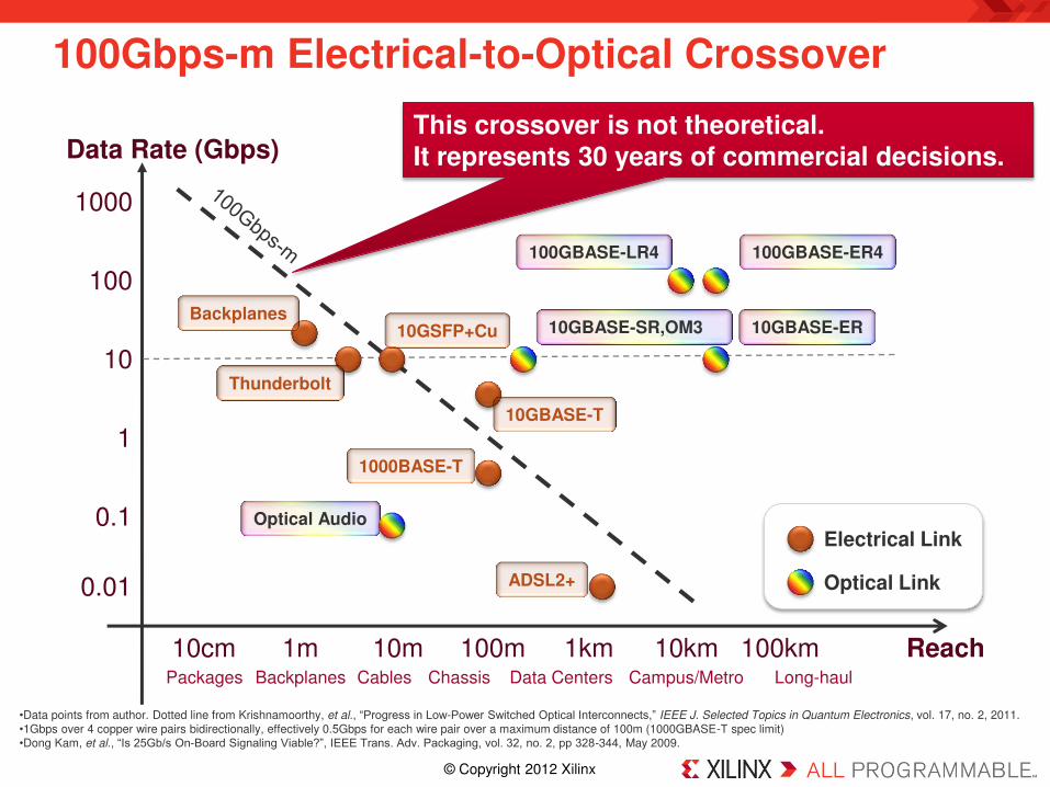
100Gbps-m Electrical-to-Optical Crossover
Reach
Data Rate (Gbps)
0.01
0.1
1
10
100
1000
1m 10m 100m 1km 10km 10cm 100km
ADSL2+
1000BASE-T
Backplanes Packages Cables Chassis Data Centers Campus/Metro Long-haul
Thunderbolt
10GBASE-T
Electrical Link
Backplanes 10GSFP+Cu
•Data points from author. Dotted line from Krishnamoorthy, et al., “Progress in Low-Power Switched Optical Interconnects,” IEEE J. Selected Topics in Quantum Electronics, vol. 17, no. 2, 2011. •1Gbps over 4 copper wire pairs bidirectionally, effectively 0.5Gbps for each wire pair over a maximum distance of 100m (1000GBASE-T spec limit) •Dong Kam, et al., “Is 25Gb/s On-Board Signaling Viable?”, IEEE Trans. Adv. Packaging, vol. 32, no. 2, pp 328-344, May 2009.
© Copyright 2012 Xilinx .
100Gbps-m Electrical-to-Optical Crossover
Reach
Data Rate (Gbps)
0.01
0.1
1
10
100
1000
1m 10m 100m 1km 10km 10cm 100km
ADSL2+
1000BASE-T
Backplanes Packages Cables Chassis Data Centers Campus/Metro Long-haul
Thunderbolt
10GBASE-SR,OM3
100GBASE-ER4
10GBASE-ER
10GBASE-T
Optical Audio
Electrical Link
Optical Link
Backplanes
100GBASE-LR4
10GSFP+Cu
This crossover is not theoretical. It represents 30 years of commercial decisions.
•Data points from author. Dotted line from Krishnamoorthy, et al., “Progress in Low-Power Switched Optical Interconnects,” IEEE J. Selected Topics in Quantum Electronics, vol. 17, no. 2, 2011. •1Gbps over 4 copper wire pairs bidirectionally, effectively 0.5Gbps for each wire pair over a maximum distance of 100m (1000GBASE-T spec limit) •Dong Kam, et al., “Is 25Gb/s On-Board Signaling Viable?”, IEEE Trans. Adv. Packaging, vol. 32, no. 2, pp 328-344, May 2009.
© Copyright 2012 Xilinx .
1
10
100
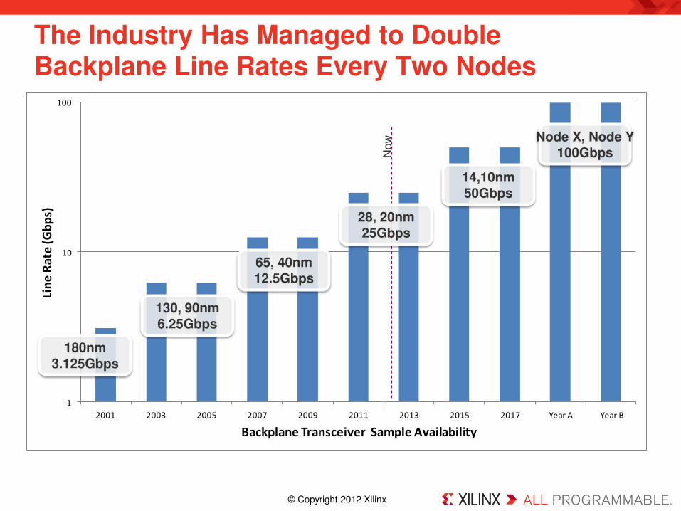
2001 2003 2005 2007 2009 2011 2013 2015 2017 Year A Year B
Lin
e R
ate
(G
bp
s)
Backplane Transceiver Sample Availability
The Industry Has Managed to Double Backplane Line Rates Every Two Nodes
180nm 3.125Gbps
130, 90nm 6.25Gbps
65, 40nm 12.5Gbps
14,10nm 50Gbps
Now
Node X, Node Y 100Gbps
28, 20nm 25Gbps

© Copyright 2012 Xilinx .
1
10
100
2001 2003 2005 2007 2009 2011 2013 2015 2017 Year A Year B
Lin
e R
ate
(G
bp
s)
Backplane Transceiver Sample Availability
The Industry Has Managed to Double Backplane Line Rates Every Two Nodes
180nm 3.125Gbps
130, 90nm 6.25Gbps
65, 40nm 12.5Gbps
14,10nm 50Gbps
Now
Node X, Node Y 100Gbps
1. Package Pin-Out Crisis Parallel-to-Serial IOs
28, 20nm 25Gbps

© Copyright 2012 Xilinx .
1
10
100
2001 2003 2005 2007 2009 2011 2013 2015 2017 Year A Year B
Lin
e R
ate
(G
bp
s)
Backplane Transceiver Sample Availability
The Industry Has Managed to Double Backplane Line Rates Every Two Nodes
180nm 3.125Gbps
130, 90nm 6.25Gbps
65, 40nm 12.5Gbps
14,10nm 50Gbps
Now
Node X, Node Y 100Gbps
2. Smaller BPs, cabled BPs, active connectors, non-NRZ signaling, etc?
1. Package Pin-Out Crisis Parallel-to-Serial IOs
28, 20nm 25Gbps

© Copyright 2012 Xilinx .
1
10
100
2001 2003 2005 2007 2009 2011 2013 2015 2017 Year A Year B
Lin
e R
ate
(G
bp
s)
Backplane Transceiver Sample Availability
The Industry Has Managed to Double Backplane Line Rates Every Two Nodes
180nm 3.125Gbps
130, 90nm 6.25Gbps
65, 40nm 12.5Gbps
14,10nm 50Gbps
Now
Node X, Node Y 100Gbps
2. Smaller e- BPs, cabled BPs, active connectors, non-NRZ signaling, etc?
1. Package Pin-Out Crisis Parallel-to-Serial IOs
28, 20nm 25Gbps
3. BPs hit 100Gbps-m crossover near end of decade?

© Copyright 2012 Xilinx .
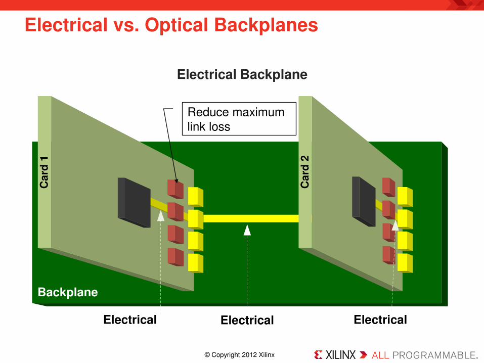
Electrical vs. Optical Backplanes C
ard
1
Ca
rd 2
Backplane
ElectricalElectrical
Electrical Backplane
© Copyright 2012 Xilinx .
Electrical vs. Optical Backplanes C
ard
1
Ca
rd 2
Backplane
ElectricalElectrical Electrical
Electrical Backplane
Reduce maximum
link loss
© Copyright 2012 Xilinx .
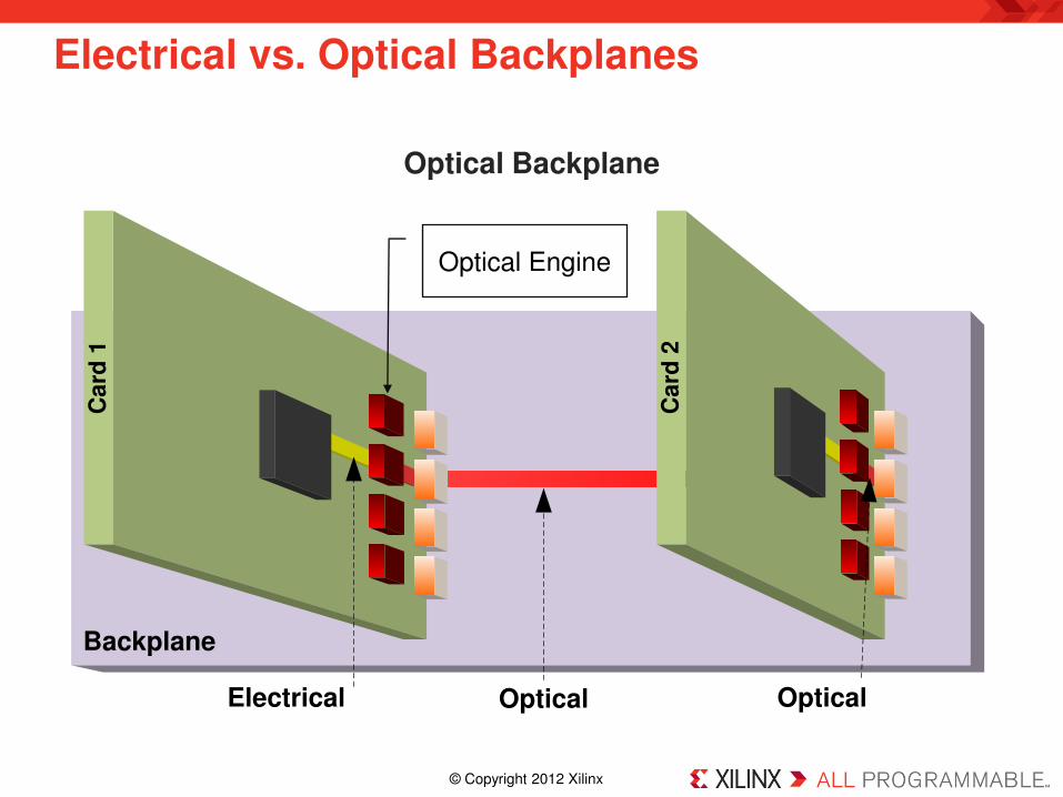
Electrical vs. Optical Backplanes C
ard
1
OpticalC
ard
2Backplane
Electrical Optical
Optical Backplane
Optical Engine
© Copyright 2012 Xilinx .
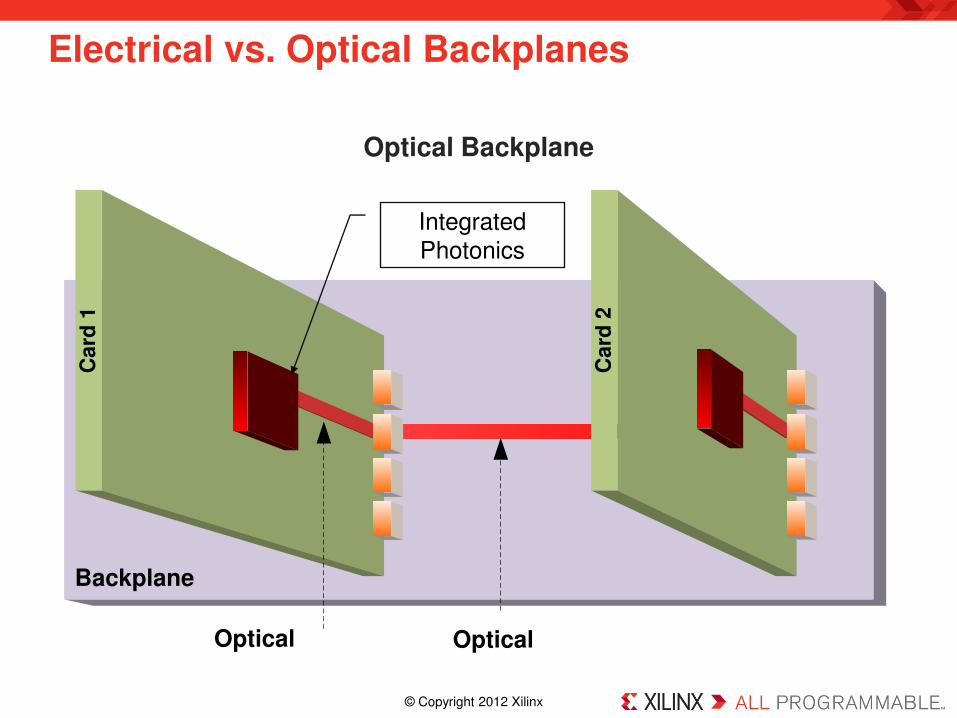
Electrical vs. Optical Backplanes
Optical Backplane
Ca
rd 1
Ca
rd 2
Backplane
OpticalOptical
Integrated
Photonics

© Copyright 2012 Xilinx .
Optical vs. Optical Backplanes (MMF vs. SMF) VCSELs: the Incumbent at 10 Gb/s
10Gb/s VCSELs over OM3 MMF
0.10.3 1 2 3 10
Reach (km)
Short
ReachLong
Reach

© Copyright 2012 Xilinx .
Optical vs. Optical Backplanes Challengers at 25 Gb/s
25Gb/s VCSELs over OM4 MMF
10Gb/s VCSELs over OM3 MMF
25Gb/s Si or InP Photonics over SMF for Warehouse Data Centers
0.10.3 1 2 3 10
Reach (km)
Short
ReachMedium Reach
(Not yet standard)
Long
Reach

© Copyright 2012 Xilinx .
Optical vs. Optical Backplanes Options in Stacked Photonics
VCSELs Co-Packaged with Logic
Lo
gic
Pa
ck
ag
e
Logic IC(Expensive
to cool)
VCSEL,PD,
Driver,AmpICs
Si or InP Photonics Co-Packaged with Logic
Lo
gic
Pa
ck
ag
e
Logic IC(100°C OK)
“Laserless” Photonic
ICs(100°C OK)
Optical
Power
Supply
MMF
MMF
SMF
SMF
VCSELs: Laser is Thermal Bottleneck 70°C 850nm MMF to 90°C 1550nm SMF?
Off-Package Optical Power Supply Evict thermal bottleneck (laser) from package.
Which technology will scale better?

© Copyright 2012 Xilinx .
Stacking Photonics Who faces up and who faces down?
PCB with Waveguides
Organic Carrier Organic Carrier
Passive Silicon Interposer with TSVs and Holes
CMOS TXVCSEL PD
CMOS RX
Lens Arrays
F. Doany, et. al., “Dense 24 TX + 24 RX Fiber-Coupled Optical Module Based on a Holey CMOS Transceiver IC,” 60th Electronic Components and Technology Conference, pp. 248-255, 2010. F. Doany, et. al., “300-Gb/s 24-Channel Bidirectional Si Carrier Transceiver Optochip for Board-Level Interconnects,” 58th Electronic Components and Technology Conference, pp. 238-243, 2008. Diagrams redrawn by Xilinx based on papers.
Connector
VCSEL PD
100u
m
Organic Carrier
90nm CMOS “Holey”RX + TX Chip
Lens Arrays
• Photonics up for fiber attach • Electronics down and with optical vias (holes)
• Photonics down for PWB • Electronics down • Si interposer with holes

© Copyright 2012 Xilinx .
Integrated-Photonics Interface Standards Standard applies to all compliant optical modules,
regardless of underlying photonics
In-Package, Decoupled from PhotonicsInterface Tied to Underlying Photonics
FP
GA
Pa
ck
ag
e
Optical Module
Se
ria
lize
r
FP
GA
De-
Se
rializ
er
OE
EO
OR
X
OT
X
FP
GA
Pa
ck
ag
e
FPGA ICPhotonic
IC(s)
Se
ria
lize
r
FP
GA
De
-S
eria
lize
r
EO
OT
X
OR
X
OE
FP
GA
Pa
ck
ag
e
FPGA ICPhotonic IC(s)
OE
Se
ria
lize
r
FP
GA
De
-S
eria
lize
r
EO
OT
X
OR
X
SMF or MMF
SMF or MMF
Example Today: CEI-28G-VSR
Common electrical inter-IC
signaling standard
© Copyright 2012 Xilinx .
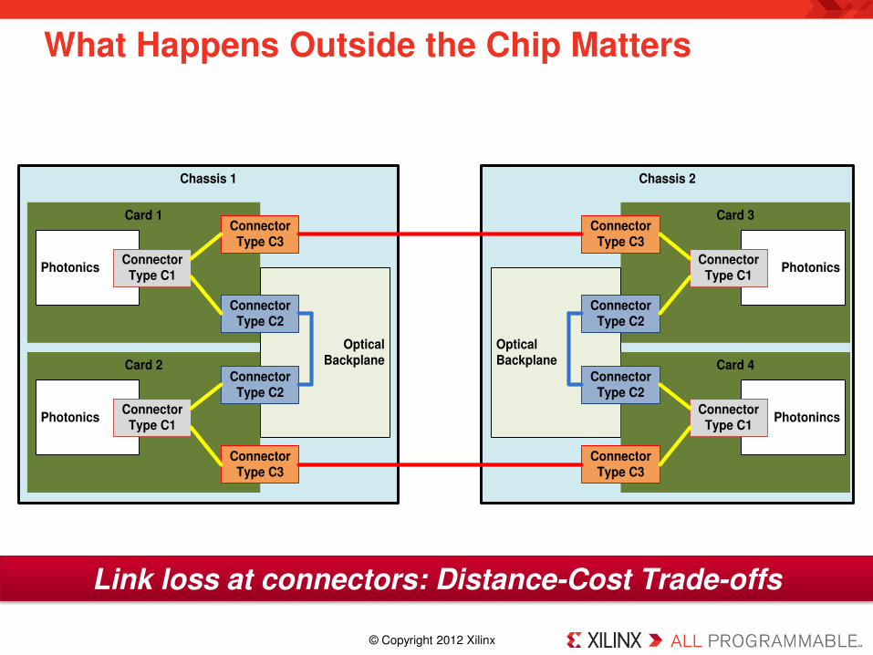
What Happens Outside the Chip Matters
Chassis 1
Card 1
PhotonicsConnectorType C1
OpticalBackplane
ConnectorType C2
ConnectorType C3
Card 2
PhotonicsConnectorType C1
ConnectorType C3
ConnectorType C2
Chassis 2
Card 3
PhotonicsConnectorType C1
OpticalBackplane
ConnectorType C2
ConnectorType C3
Card 4
PhotonincsConnectorType C1
ConnectorType C3
ConnectorType C2
Link loss at connectors: Distance-Cost Trade-offs

© Copyright 2012 Xilinx .
Opto-Electronics Supply Chain Needed
Package Substrate
28nm FPGA & Interposer
Bump, Die separation
CoC/CoWoS, & Assembly
Final Test of Packaged Part
IBIDEN
FPGA, Interposer, & Package Design
Opto-Electronics Design
[Names Here]
Opto-Electronics OSAT
[Names Here]
Xilinx Stacked-Silicon Supply Chain

© Copyright 2012 Xilinx .
Summary
1 Electrical vs. Optical Backplanes Mainstream backplanes to reach crossover near end of decade
2 Optical vs. Optical Backplanes Choice of VCSELs, InP, and Si Photonics impacts costs & scalability
3 Chip-stacking is just a means to an end Electrical-to-optical migration: focus on systems and supply chain