optics of nanostructures: science, technology, applications sergey v. gaponenko
DESCRIPTION
Optics of Nanostructures: Science, Technology, Applications Sergey V. Gaponenko. Institute of Molecular and Atomic Physics National Academy of Sciencs of Belarus. Institute of Molecular and Atomic Physics. Established in 1992 (separated from th e Inst. Physics) - PowerPoint PPT PresentationTRANSCRIPT

Optics of Nanostructures:Optics of Nanostructures:Science, Technology, Science, Technology,
ApplicationsApplications
Sergey V. GaponenkoSergey V. Gaponenko
Institute of Molecular and Atomic Institute of Molecular and Atomic PhysicsPhysics
National Academy of Sciencs of National Academy of Sciencs of BelarusBelarus

Institute of Molecular and Institute of Molecular and Atomic PhysicsAtomic Physics
Established in 1992 (separated from the Inst. Physics)
Staff: 160 total (30 Dr. of Sci, 70 Ph.D)
Research topics:• Plasma physics and atomic spectroscopy• Molecular spectroscopy• Photobiophysics• Physics of nanostructures
12 research laboratories
Journal of Applied Spectroscopy publisher (since 1964)

Basic PrinciplesBasic Principles
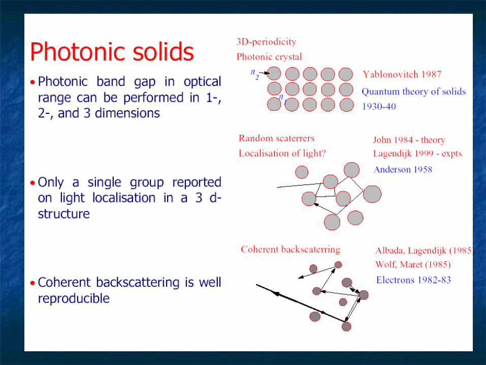
Photonic crystal ideologyPhotonic crystal ideology
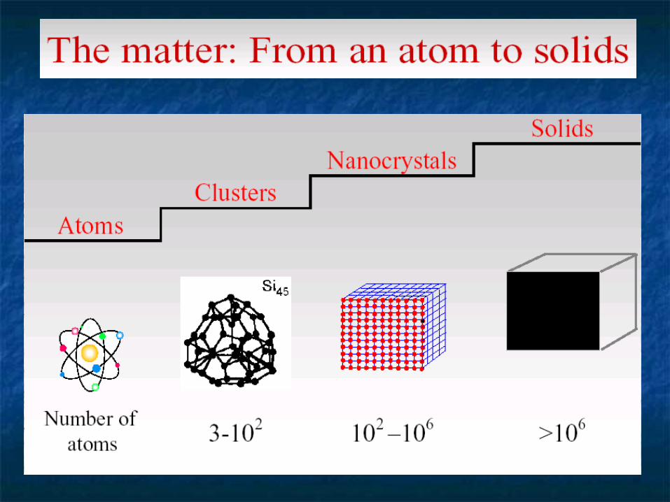
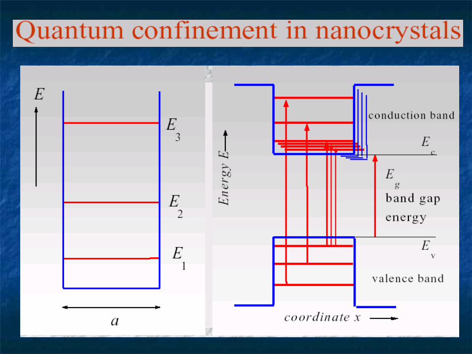
Quantum size effects in Quantum size effects in semiconductor nanocrystalssemiconductor nanocrystals
Surface enhanced optical processesSurface enhanced optical processes

Photonic crystalsPhotonic crystals


Nanoporous alumina Nanoporous alumina developed at BSUIRdeveloped at BSUIR
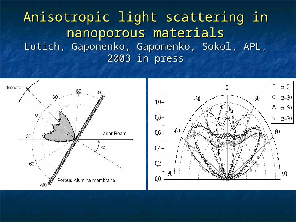
Anisotropic light scattering in Anisotropic light scattering in nanoporous materialsnanoporous materials
Lutich, Gaponenko, Gaponenko, Sokol, APL, 2003 Lutich, Gaponenko, Gaponenko, Sokol, APL, 2003 in pressin press

Quantum size effects in Quantum size effects in semiconductor semiconductor nanocrystalsnanocrystals


Absorption
Lum
ines
cenc
e in
tens
ity (a
.u.)
Abs
orpt
ion
(lg I
0/I)
Wavelength (nm)400 600 800
0
1
2
3
4
5
Luminescence
CdS:Mn nanocrystals

Light convertor for Si photodetectorsLight convertor for Si photodetectorsMain advantage versus organic luminophores:Main advantage versus organic luminophores:
high photostabilityhigh photostability
300 350 400 450 500 550 600 650 700 750 8000.0
0.5
1.0
1.5
2.0
Si-photodetector withUV sensitive coating
Photo
curr
ent (A
)
Wavelength (nm)
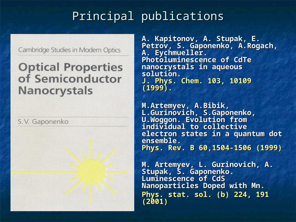
Principal publicationsPrincipal publications
A. Kapitonov, A. Stupak, E. Petrov, A. Kapitonov, A. Stupak, E. Petrov, S. Gaponenko, A.Rogach, A. S. Gaponenko, A.Rogach, A. Eychmueller. Photoluminescence Eychmueller. Photoluminescence of CdTe nanocrystals in aqueous of CdTe nanocrystals in aqueous solution. solution. J. Phys. Chem. 103, 10109 (1999).J. Phys. Chem. 103, 10109 (1999).
M.Artemyev, A.Bibik, L.Gurinovich, M.Artemyev, A.Bibik, L.Gurinovich, S.Gaponenko, U.Woggon. Evolution S.Gaponenko, U.Woggon. Evolution from individual to collective from individual to collective electron states in a quantum dot electron states in a quantum dot ensemble. ensemble. Phys. Rev. B 60,1504-1506 (1999)Phys. Rev. B 60,1504-1506 (1999)
M. Artemyev, L. Gurinovich, A. M. Artemyev, L. Gurinovich, A. Stupak, S. GaponenkoStupak, S. Gaponenko. . Luminescence of CdS Luminescence of CdS Nanoparticles Doped with MnNanoparticles Doped with Mn. . PPhys. stat. sol. (b) 224, 191 (2001)hys. stat. sol. (b) 224, 191 (2001)


Surface enhanced optical Surface enhanced optical processes processes
Enhanced Raman scattering Enhanced Raman scattering
Enhanced PhotoluminescenceEnhanced Photoluminescence

Malashkevich et al, in pressMalashkevich et al, in press
400 500 600 700
5000
10000
15000
20000
25000
30000
Eu luminescence enhancement
in presence of silver colloids
Wavelength (Nanometers)
Inte
nsi
ty
1
2
3
7% мол. Eu2O
3
1 - no Ag.
2 - 0,5 % AgNO3.
3 - 5 % AgNO3.


High-sensitive SERS molecular High-sensitive SERS molecular analysysanalysys
Gaponenko, Gaiduk, Kulakovich et al. JETP Lett. 2001, 74, 324.

Basic TechnologiesBasic Technologies
Electrochemical etchingElectrochemical etching
Colloidal chemistryColloidal chemistry
Sol-gel processesSol-gel processes
High-energy plasma flow High-energy plasma flow processesprocesses

Nanoporous aluminaNanoporous aluminaBSUIRBSUIR

CdSe nanocrystalsCdSe nanocrystals ССdTedTe nanocrystalsnanocrystals Gaponenko et al. Gaponenko et al. Gaponenko et al. Gaponenko et al.
J. Appl. Phys. 1995, J. Appl. Phys. 1995, JETP lett. 1998JETP lett. 1998
In cooperation with Belarussian Sate University

Colloidal crystalsColloidal crystalsPetrov, Bogomolov, Kalosha, Gaponenko, PRL Petrov, Bogomolov, Kalosha, Gaponenko, PRL
19981998cooperation with Russian Academy of Sciences
and Inst. Powder Metallurgy

Metal colloidsMetal colloids
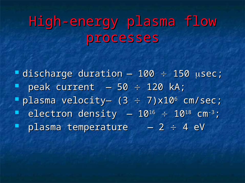
High-energy plasma flow High-energy plasma flow processesprocesses
discharge durationdischarge duration — 100 — 100 150 150
sec;sec; peak currentpeak current — 50 — 50 120 kA; 120 kA; plasma velocityplasma velocity — (3 — (3 7)x10 7)x1066
cm/sec;cm/sec; electron densityelectron density — 10— 101616 10 101818 cm cm-3-3;; plasma temperatureplasma temperature — 2 — 2 4 eV 4 eV
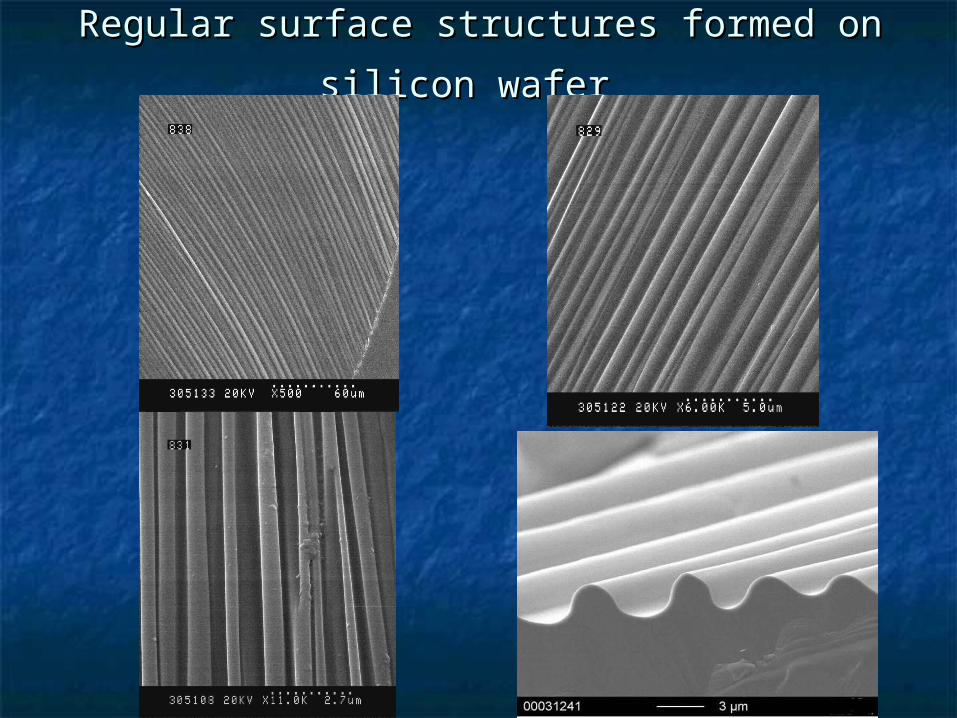
Regular surface structures formed on silicon Regular surface structures formed on silicon
waferwafer

TasksTasks
• Novel luminophores and efficient light Novel luminophores and efficient light emitting devicesemitting devices
• Spectral transformers for silicon solar cells Spectral transformers for silicon solar cells and photodetectorsand photodetectors
• Ultrasensitive chemical analysisUltrasensitive chemical analysis
• Si surface processingSi surface processing

Optical data coding and security Optical data coding and security systemssystems

Spectral portraits of numbersSpectral portraits of numbers

Current projectsCurrent projects National program “Electronics”National program “Electronics” National program “Nanotechnologies”National program “Nanotechnologies” National program “Plasma dynamics”National program “Plasma dynamics” National Basic Res. Fnd. Projects (5)National Basic Res. Fnd. Projects (5) International INTAS projects (2 projects)International INTAS projects (2 projects) NATO for Peace projectNATO for Peace project Int. Sci. Techn. Center projectInt. Sci. Techn. Center project Volkswagen Shiftung projectVolkswagen Shiftung project Cooperaton agreement with Swiss Sherer InstituteCooperaton agreement with Swiss Sherer Institute European network of excellence “Nanophotonics”European network of excellence “Nanophotonics”