organic light emitting diodes (oleds) for general illumination
TRANSCRIPT
Organic Light Emitting Diodes (OLEDs) for General Illumination Update 2002
AA NN OO II DD AA TT EE CC HH NN OO LL OO GG YY RR OO AA DD MM AA PP
Date August, 2002
Sponsored by: Optoelectronics Industry Development Association (OIDA)
Department of Energy – Office of Building Technology, State and Community Programs
Edited by: Milan Stolka, Consultant
Published by:
1133 Connecticut Avenue, NW #600 Washington, DC 20036 Ph: 202-785-4426 ♦ Fax: 202-785-4428 Web: http://www.OIDA.org OIDA Member Use Only
2002 OIDA Optoelectronics Industry Development Association
All data contained in this report is proprietary to OIDA and may not be distributed in either original or reproduced form to anyone outside the client’s internal organization within five years of the report
date without prior written permission of OIDA.
Published by: Optoelectronics Industry Development Association
1133 Connecticut Ave., NW Suite 600 Washington, DC 20036-4380
Ph: (202) 785-4426; Fax: (202) 785-4428 Internet: http://www.oida.org
OIDA OLEDs Update 2002 1
The US Department of Energy's Office of Building Technology (BT) is facilitating a public-private partnership to develop a series of technology roadmaps. The roadmaps identify key goals and strategies for improvements in buildings and equipment. The roadmap, or plan, is a fundamental component of the BT strategic plan and will help to align government resources with the high priority needs identified by industry and OIDA. One such priority need at BT is the reduction of energy consumed for general illumination. Roadmaps such as this will guide cooperation among public and private researchers, lighting companies, private and state universities and State and federal offices. This roadmap effort, co-sponsored by the US Department of Energy's Office of Building Technology and OIDA and executed by OIDA (Optoelectronic Industry Development Association), has produced a research plan for organic light emitting diodes, in addressing the general illumination market.
The latest study at the US Department of Energy (1) shows that 7.2 Quads (quadrillions of British Thermal Units - BTUs) were consumed in 2001 to provide lighting to commercial, residential and industrial buildings and stationary fixtures in the USA. This represents about 20% of all the electricity produced in the United States. This level of consumption, which is steadily increasing due to the raising affluence of our society, is not sustainable.
It is now accepted that there is a need to develop viable methodologies to conserve 50% of the electric lighting load by the year 2010. This cannot be achieved only by energy conservation, advanced electronic controls and more efficient lighting fixtures. The main enabler of the energy conservation effort will be new lighting technologies such as SSL (Solid State Lighting), specifically Light Emitting
Diodes (LEDs) and Organic Light Emitting Diodes (OLEDs).
SSL have the promise of replacing the existing light sources, and at the same time
* contribute to the reduction of energy consumption,
* positively affect the greenhouse effect by reducing the emission of CO2,
* create new industry and new jobs.
OLEDs will eventually displace area (distri-buted) sources such as fluorescent lamps, but in many applications also incandescent lamps. OLEDs will also create new lighting possibilities by enabling large area illumination sources, panels, ceilings, walls, partitions, fabrics etc.
OLEDs have all the attributes to effectively compete with incandescent and fluorescent lighting, because they will
* be much more energy efficient,
* generate pleasing white light with high CRI (Color Rendition Index),
* enable "designer color" on demand,
* provide new design opportunities for architects.
There are still many technical obstacles that have to be overcome before OLEDs become a viable alternative to fluorescent and incan-descent lighting. It has been the intent of OIDA and the DOE to develop a technology roadmap for OLEDs, which would identify the critical roadblocks and suggest pathways for overcoming those roadblocks. The OIDA road-mapping effort was first reviewed in the OIDA and the Department of Energy co-sponsored OLED workshop, which was held on Nov. 30 and Dec. 1, 2000 in Berkeley, CA, and then in another workshop held on April 5, 2002 at the
1. Executive Summary
OIDA OLEDs Update 2002 2
same location. Both workshops were attended by key technical experts on OLEDs.
These workshops had several objectives:
* To reach the industry consensus on the application of OLEDs in Solid State Lighting,
* To enumerate the technologies that need to be developed and improved to support the goal that OLEDs become the source of light for general illumination
* To identify and examine major technical problems and roadblocks standing in the way for OLEDs to become a technology of choice for general lighting and provide the basis for developing a technology roadmap to achieve this goal.
* To identify long-term research issues.
The conclusions of the workshops, the outline of the major research areas, and recommendations are included in Section 5.
It is the opinion of the OLED experts and workshops participants that no fundamental obstacles now exist that would prevent OLEDs from achieving the above goal. In view of the recent progress in improving the device efficiency and useful life, all participants share the optimism that the goal will be achieved.
However, many incremental advances and breakthroughs must be made in the technology. These advances, which can overcome what can be called “incremental roadblocks”, will be
made only if substantial research is carried out to enhance the understanding of the function of OLEDs and of the processes that cause their instability. Also, many novel high performance robust materials have to be synthesized, and the device architecture has to be optimized. The lack of commercially available specialty materials is an obstacle.
Although the OLED experts had different outlooks, it was a general consensus that without a meaningful industry / government / academia collaboration and a substantial infusion of funds it would take 12 – 15 years before the commercialization of OLEDs for general lighting could be considered in the USA. In that case, it is generally believed that the Pacific Basin, where the effort is already supported by the governments, would be ahead of the US and take the leadership role. However, with appropriate incentives, financial stimulation, enhancement of the intellectual property, and within the properly formulated framework of collaboration between the government, industry and academia, OLEDs could be developed within 5-8 years for the use in general lighting, and the US leadership in this area could be assured.
OIDA OLEDs Update 2002 3
Table of Contents
1. Executive Summary 1
2. Introduction 5 2.1 Background 7 2.2 Devices 8 2.3 Materials 9 2.4 White Light from OLEDs 9 2.5 Challenges and Critical Issues 9
3. OLED Applications and Markets 10 3.1 Overview of Application 10 3.2 Applications of OLEDs (No Breakthrough Required) 11 3.3 Applications Convertible to OLEDs (Require Breakthroughs) 12 3.4 New Applications that Could be Enabled by OLEDs 12 3.5 Factors Affecting Penetration into the General Lighting Market 12
4. Performance and Cost Goals for OLEDs 13 4.1 Performance Goals 14 4.2 Cost Goals 15
5. Technological Challenges and OIDA Technology Roadmap 16 5.1 Technical Issues 17 5.1.1 Device Architecture 17 5.1.2 Operational Lifetime 20 5.1.3 Device Efficiency 25 5.1.4 White Color OLEDs 30 5.1.5 Shelf Life 41 5.1.6 Current Distribution Over Large Areas 43 5.1.7 Electrodes 43 5.2 Manufacturing Issues 45 5.2.1 Synthesis of Materials 45 5.2.2 Large Area Coating and Deposition 46 5.2.3 Plastic Substrates 47 5.3 Summary: Technology Roadblocks. Integration 48 5.4 OLED Workshops Conclusions and Recommendations 49 5.4.1 Current Status of OLEDs 50
OIDA OLEDs Update 2002 4
5.4.2 Strategy for making OLEDs the Technology of Choice for General Lighting 52 5.4.3 Long-Term Research and Development Issues 53 5.4.4 Goals and Milestones 54 5.4.5 List of Attendees at the OIDA Solid State Lighting Workshops 61
6 Acknowledgement 67
Appendix A: References 68
Appendix B: Glossary of Terms 71
Appendix C: White Color OLEDs (by Yoshi Ohno) 72
OIDA OLEDs Update 2002 5
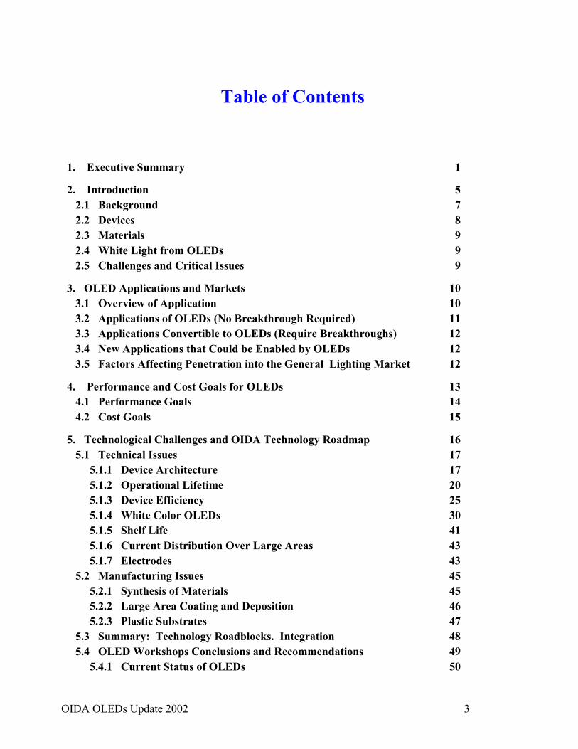
Of all countries, USA is by far the largest consumer of energy. In 2001, about 36 Quads of electricity was produced in the US at a cost of $252 billion. 20% of that energy, which represents 7.2 Quads, was used for lighting at a cost of about $50 billion (1). The existing sources of light are inefficient. At present, only about 30% of the energy consumed for general illumination is used to generate light; the rest is wasted as heat. Incandescent lamps, light bulbs, consume 45% of all the lighting energy and yet produce only 14% of light, measured in lumens. About 90% of the energy goes to the production of heat. Fluorescent lamps are about four times more energy efficient, but still, a significant fraction of the used energy is wasted. Other sources of light, halogen lamps, high intensity discharge lamps, have only a limited use and are not much more efficient than the fluorescent lamps. Not much progress has been made in the energy efficiency of all the conventional sources of light within the past 30 - 50 years. These sources have reached the technological maturity, and little can be done to make them more
efficient. Therefore, new lighting technologies are desirable and necessary.
One of the new lighting technologies which emerged within the past two decades and has the potential of becoming more energy-efficient then the existing light sources, is the Solid State Lighting technology of Organic Light Emitting Diodes (OLEDs).
The available data about OLEDs and technical projections indicate that the amount of energy needed to generate the same amount of light can be eventually reduced by up to 50%. If the consumption of electric energy used for lighting is reduced by the desired 50%, the savings to the society would amount to approximately $25B per year (1). In addition to the savings, less consumed energy would amount to less produced energy and, consequently, less pollution of water and air. According to the latest estimates, the use of electricity may be reduced by 50% by the year 2020, sparing the atmosphere some 45 million tons of carbon emissions annually. The potential savings also depends on how quickly
Tera-Lumen Hours / Annum
0 5000 10000 15000 20000
Commercial
Industrial
Residential
Stationary* Incandescent
Fluorescent
High IntensityDischarge
2001 Estimate: 7.2 quads
2. Introduction
Fig. 1. Annual light production by source: All building sectors (1)
OIDA OLEDs Update 2002 6
and to what extend these developments occur (2). This study also indicates that it is primarily the price breakthrough that will facilitate the market penetration of the new sources of light. In other words, even though the technological advances may lead to significant reduction of energy, the market will not accept SSL unless the cost is reduced as well. If SSL achieves a price breakthrough, far more energy will be saved.
Today, incandescent light bulbs dominate the residential and light industrial lighting market where the initial cost and aesthetics are the key drivers. Fluorescent lamps are used in the commercial sector where the combined cost of the lighting fixtures and the consumed energy is the principal driver.
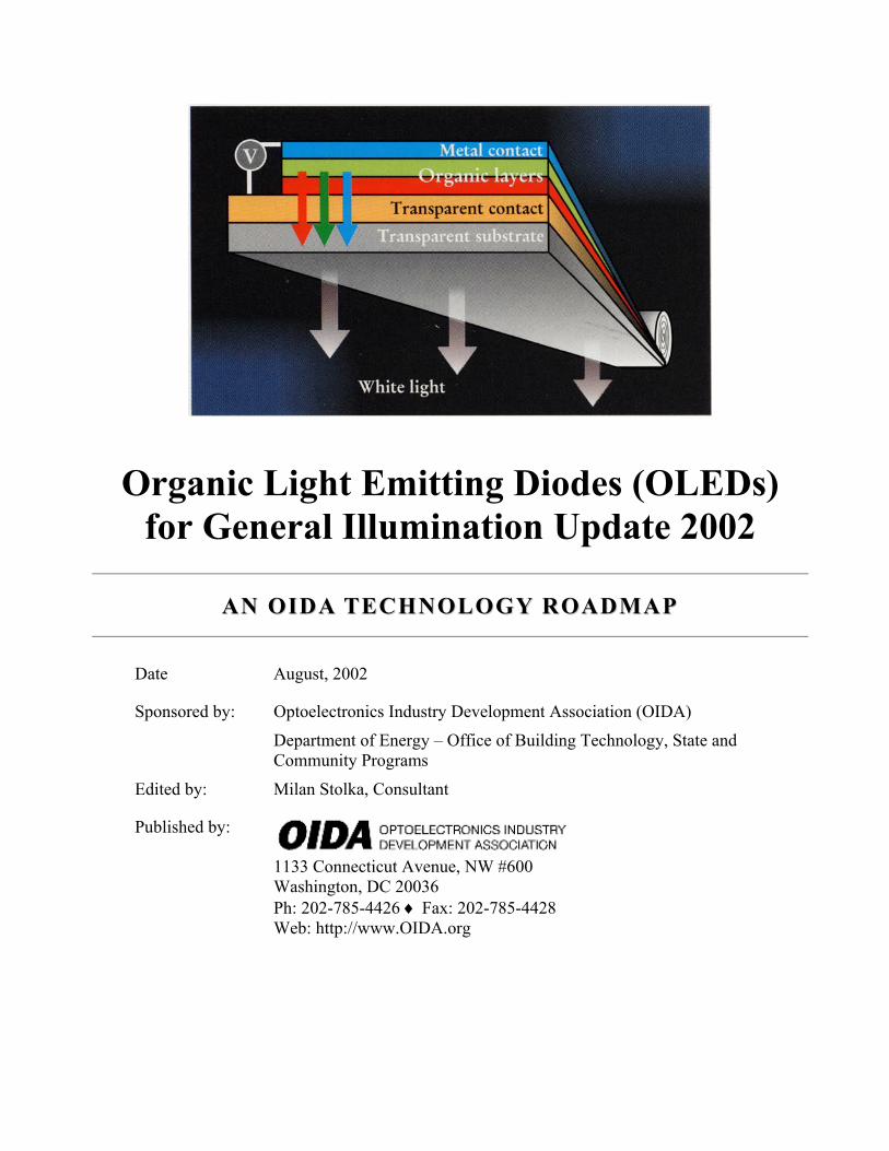
OLEDs are unconventional, large area thin-film, nearly two-dimensional devices. They are distributed (diffused) light sources, distinctly different from point sources such as light bulbs. Also, OLEDs will operate at very low voltages, of the order of 3 - 5 V. Therefore, the introduction of OLEDs as sources of light for general lighting applications will cause a major paradigm shift in the lighting industry. Not only a new lighting infrastructure will be required, but also many new jobs will be created. While significant research is still needed, OLEDs will soon achieve the efficiency to compete directly with incandescent sources (light bulbs).
Experimental OLEDs are already more energy-efficient than incandescent lamps. The luminous efficiency of light bulbs is about 13 - 20 lm/W but the latest experimental green-emitting OLEDs already have luminous efficiency of 76 lm/W, albeit at low luminances(3). The development is on track for OLEDs to effectively compete even with fluorescent lamps, which have the luminous efficiency of 50 - 100 lm/W.
One big advantage of OLEDs is the ability to tune the light emission to any desired color, and
any shade of color or intensity, including white. Achieving the high color rendition index (CRI) near 100 (the ability to simulate the most pleasing white color, sunlight), is already within the reach of OLEDs. Another advantage of OLEDs is that they are current-driven devices, where brightness can be varied over a very wide dynamic range and they operate uniformly, without flicker. All this has created a great deal of optimism that OLEDs will be accepted and welcome by the general public - as long as they are inexpensive.
Yet another advantage of OLEDs is that they could be deposited on any substrate: glass, ceramics, metal, thin plastic sheets, fabrics, flexible and conformable substrates, etc., and therefore, could be fabricated in any shape and design. This will open new architectural and design possibilities. Freedom to produce sources of any shape or color will create radically new illumination culture.
In a nutshell, OLEDs have a potential of being large area, white-light sources that are
* bright, power-efficient and long lived, emitting pleasing white light
* ultra-thin, light weight, rugged, and conformable
* inexpensive
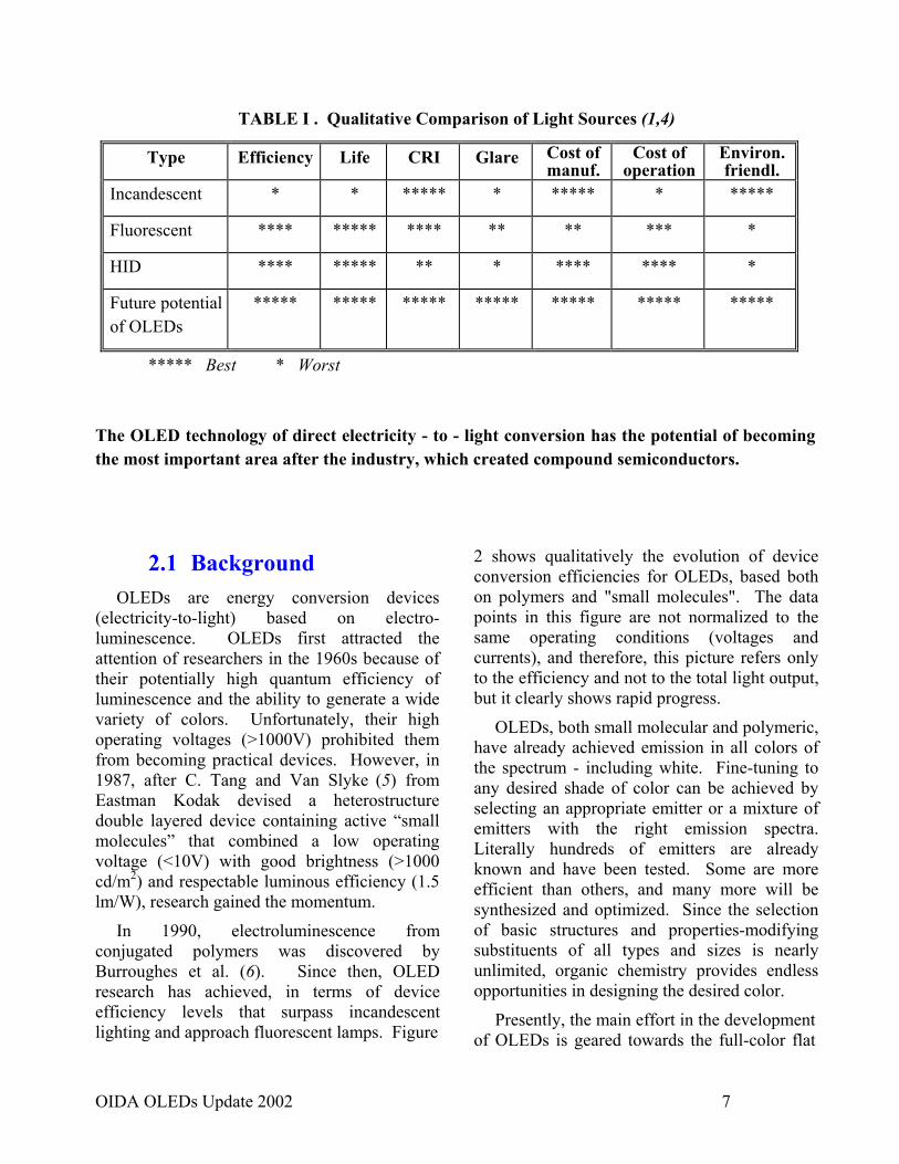
As the Table I indicates, OLEDs will have a number of advantages over the existing light sources.
This qualitative comparison is based on the assumption that the development of OLEDs will be successful. Monumental challenges, however, still exist to reach the goal. Over the next 5 years, the lighting market will grow to about $40B/y. Based on the novel features, OLEDs may soon capture 10% of that market. As the efficiency and cost approach the targets of fluorescent lamps, 50% of the market may be captured in 10-12 years.
OIDA OLEDs Update 2002 7
TABLE I . Qualitative Comparison of Light Sources (1,4)
Type Efficiency Life CRI Glare Cost of manuf.
Cost of operation
Environ. friendl.
Incandescent * * ***** * ***** * *****
Fluorescent **** ***** **** ** ** *** *
HID **** ***** ** * **** **** *
Future potential of OLEDs
***** ***** ***** ***** ***** ***** *****
***** Best * Worst
The OLED technology of direct electricity - to - light conversion has the potential of becoming the most important area after the industry, which created compound semiconductors.
2.1 Background OLEDs are energy conversion devices
(electricity-to-light) based on electro-luminescence. OLEDs first attracted the attention of researchers in the 1960s because of their potentially high quantum efficiency of luminescence and the ability to generate a wide variety of colors. Unfortunately, their high operating voltages (>1000V) prohibited them from becoming practical devices. However, in 1987, after C. Tang and Van Slyke (5) from Eastman Kodak devised a heterostructure double layered device containing active “small molecules” that combined a low operating voltage (<10V) with good brightness (>1000 cd/m2) and respectable luminous efficiency (1.5 lm/W), research gained the momentum.
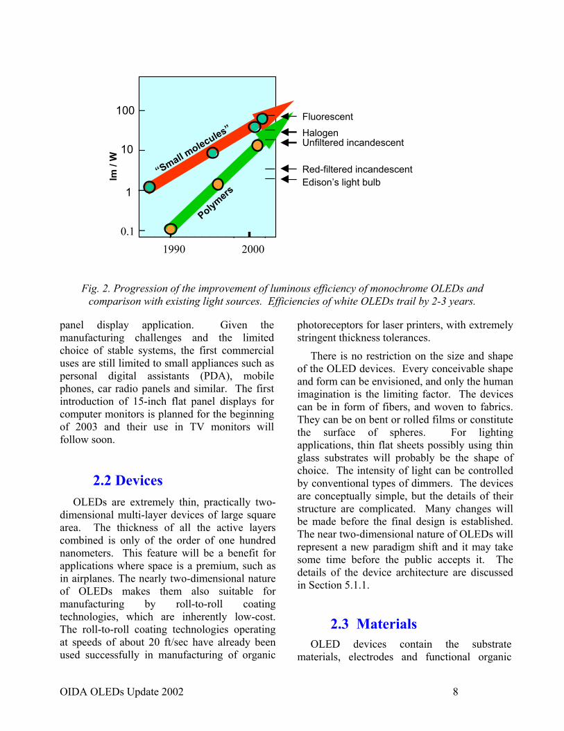
In 1990, electroluminescence from conjugated polymers was discovered by Burroughes et al. (6). Since then, OLED research has achieved, in terms of device efficiency levels that surpass incandescent lighting and approach fluorescent lamps. Figure
2 shows qualitatively the evolution of device conversion efficiencies for OLEDs, based both on polymers and "small molecules". The data points in this figure are not normalized to the same operating conditions (voltages and currents), and therefore, this picture refers only to the efficiency and not to the total light output, but it clearly shows rapid progress.
OLEDs, both small molecular and polymeric, have already achieved emission in all colors of the spectrum - including white. Fine-tuning to any desired shade of color can be achieved by selecting an appropriate emitter or a mixture of emitters with the right emission spectra. Literally hundreds of emitters are already known and have been tested. Some are more efficient than others, and many more will be synthesized and optimized. Since the selection of basic structures and properties-modifying substituents of all types and sizes is nearly unlimited, organic chemistry provides endless opportunities in designing the desired color.
Presently, the main effort in the development of OLEDs is geared towards the full-color flat
OIDA OLEDs Update 2002 8
panel display application. Given the manufacturing challenges and the limited choice of stable systems, the first commercial uses are still limited to small appliances such as personal digital assistants (PDA), mobile phones, car radio panels and similar. The first introduction of 15-inch flat panel displays for computer monitors is planned for the beginning of 2003 and their use in TV monitors will follow soon.
2.2 Devices OLEDs are extremely thin, practically two-
dimensional multi-layer devices of large square area. The thickness of all the active layers combined is only of the order of one hundred nanometers. This feature will be a benefit for applications where space is a premium, such as in airplanes. The nearly two-dimensional nature of OLEDs makes them also suitable for manufacturing by roll-to-roll coating technologies, which are inherently low-cost. The roll-to-roll coating technologies operating at speeds of about 20 ft/sec have already been used successfully in manufacturing of organic
photoreceptors for laser printers, with extremely stringent thickness tolerances.
There is no restriction on the size and shape of the OLED devices. Every conceivable shape and form can be envisioned, and only the human imagination is the limiting factor. The devices can be in form of fibers, and woven to fabrics. They can be on bent or rolled films or constitute the surface of spheres. For lighting applications, thin flat sheets possibly using thin glass substrates will probably be the shape of choice. The intensity of light can be controlled by conventional types of dimmers. The devices are conceptually simple, but the details of their structure are complicated. Many changes will be made before the final design is established. The near two-dimensional nature of OLEDs will represent a new paradigm shift and it may take some time before the public accepts it. The details of the device architecture are discussed in Section 5.1.1.
2.3 Materials OLED devices contain the substrate
materials, electrodes and functional organic
Red-filtered incandescent
Unfiltered incandescent
0.1
1
10
100lm
/ W
Fluorescent
Halogen
Edison’s light bulb
1990 2000
Polymers
“Small molecules”
Fig. 2. Progression of the improvement of luminous efficiency of monochrome OLEDs and comparison with existing light sources. Efficiencies of white OLEDs trail by 2-3 years.
OIDA OLEDs Update 2002 9
substances. All are environmentally safe. Two types of electrodes are used. An extremely thin layer of indium - tin oxide (extremely thin, because it has to be optically transparent), is used as anode. Low work-function metals such as Mg, Li, and their alloys with Ag, and in some cases Al, are now used as cathodes. Several types of organic materials are used in the functional layers: Polymers or small molecules that transport injected charges to the recombination zone, fluorescent or recently introduced more efficient phosphorescent dopants that emit light, and charge-injection modifying compounds, such as conducting polymers near the anode or salts such as LiF or CsF etc near the cathode. The charge transporting polymers are typically polyconjugated, such as derivatives of polyphenylene vinylene. The small molecules are substituted aromatic amines for hole transport and a variety of polynuclear aromatic complexes with high electron affinity for electron transport. In some cases, the charge transporting polymers or small molecules themselves assume the role of emitters. These materials can be deposited in many separate layers or mixed into one or several layers. Organic chemistry offers an endless variety of structures, and therefore, the choices of charge transporters, emitters and other dopants are virtually unlimited.
Polymeric OLEDs have the advantage that the active layers can be deposited from solution, while in "small molecule" OLEDs, the active layers are typically deposited by vapor deposition techniques. The chemical nature of the OLED materials and the performance and stability issues are discussed in Section 5.1.
2.4 White Light from OLEDs OLEDs are uniquely suitable as sources of
white light. The structure of light emitting fluorescence or phosphorescence additives can be tailored to emit any desired color (see section 5.1). Mixing light from two or more sources
(dopants or layers) gives light whose color is determined by the weighted average of the CIE coordinates of these sources. Given the enormous variety of known and yet-to-be synthesized dopants, both fluorescent and phosphorescent, with broad emission spectra of choice, practically any shade of white or any "temperature" of white light can be generated in OLEDs. Many devices have already been made in the laboratory scale and tested and some of them almost perfectly simulate the sunlight. The methods of generating white light are described in Sections 5.1.4. and 5.1.5.
2.5 Challenges and Critical Issues Even though remarkable progress has been
made, OLEDs still face great challenges before commercialization as white-light sources can be even considered. OLEDs have already achieved power conversion efficiencies close to those needed for energy efficient operation, but only for the green and red light, and with insufficient luminances. Other colors are still far beyond. The peak brightness can be greater than several hundreds of thousands cd/m2, but these devices degrade very quickly. The operating voltages can be as low as the desired 2.6 - 4 V but the luminances are still too low under those voltages. For white light and the desired luminance, the passing electric currents are still too high, and the power conversion efficiencies are low. The useful lifetime of white-light emitting devices with the desired luminance needs to be increased by more than one order of magnitude. The surface area of the largest devices made to date is only of the order of a couple of square inches, while the illumination panels will have to cover several square feet. The uniformity of these devices is far worse than desired, etc., etc.
The technological issues facing OLEDs can be summarized into the four main categories:
Operational life
Power conversion efficiency
OIDA OLEDs Update 2002 10
Cost of manufacturing
The lack of infrastructure
Specifically, to effectively compete with, and eventually displace fluorescent lighting, these challenges are:
(1) Efficacy improvement to obtain 120 lm/W for white light for a 1000 lm white source and useful life 20,000 hrs (2) Cost of manufacturing so as to be
lower than for traditional light sources (3) Development of new infrastructure including powering of high current-low voltage distributed sources, new industries and technologies that are enabled by attributes of OLED SSL.
Recent advances, which will be discussed in the following sections, created a great deal of optimism in the OLED community. None of these challenges is insurmountable.
3.1 Overview of Applications
We have only begun to imagine what OLED technology can create in the way of products, applications, job creation and new markets. The technology will not only improve existing methods of illumination but will create entirely new lighting product possibilities. OLEDs will create new markets where distributed sources of light can be applied, or are even desirable. Incandescent lights now dominate the residential market, primarily because incandescent lighting is almost natural white and, therefore, it offers near perfect color rendition demanded by the general population. The pleasing, near white color emitted by incandescent light is enabled by the high temperature of the filaments. Also, from the consumer point of view, the low "first cost" is attractive. To a typical consumer, the total cost of light is not important. On the other hand, cost conscious commercial establishments use more energy-efficient fluorescent lamps.
OLEDs have the potential to make an inroad into both markets.
First, OLEDs will offer an unparalleled capability to tune the output color to virtually any shade or tint the customer may ever
demand, including white with near-perfect color rendition. This feature will attract the "quality conscious" customer, primarily for residential applications.
Second, OLEDs will ultimately be so energy efficient that they will attract the "cost-conscious" customers in the commercial applications, where fluorescent lighting is now predominant. In both markets OLEDs will offer lower cost of ownership and will offer many other advantages over the existing light sources, such as new fixture design opportunities.
The focus of the OLED industry is now on the application in displays. The first application other than in displays will probably be back-lighting - (such as in LC displays), and, on a larger scale, for location maps in shopping malls, advertizing signs, etc. Light weight, thinness, and flexibility will allow different mounting options, which in turn will motivate a shift from the conventional light bulbs.
In traditional lighting, OLEDs will have a difficult time competing for the next 7-10 years. However, in non-traditional applications, OLEDs will have a clear performance edge. Example: Owners of upscale houses are willing to spend more than $1,000 for a light fixture with < $20 for bulbs. If OLED "wallpaper" is
3 OLED Applications and Markets
OIDA OLEDs Update 2002 11
available for the same cost, with a dimmer and color selector (for mood lighting), it will command a premium price. At $1,000 for 200 sq. feet of OLED wallpaper ($5 per sq. ft.) - more than wallpaper but cheaper than wallpaper + the light fixture. Half of the $5 will go for installation, which leaves $2.50 for materials. With the advancement of roll-to-roll coating of the OLED devices, this number is attainable.
One can envision that commercial buildings can be lighted by ceiling or wall panels of OLED materials, by partitions, new types of large area fixtures, etc. The desired luminances will vary according the application. For example, fixtures designed to replace the existing fluorescent lamps with the same square area will have to have luminances of the order of 2,500 cd/m2 but if larger areas are preferred, the desired luminances could be less. If a larger portion of the ceiling is covered by a light source, the luminances can be as low as 800 - 850 cd/m2. In situations where glare is undesirable, the maximum luminance will have to be about 850 cd/m2. Distributed light source will not produce shadows.
The focus on displays to some extend slows down the development of OLEDs for general lighting, because the development priorities are different. Under these circumstances, it is believed that without a meaningful industry / government / academia collaboration and a substantial infusion of funds it would take 12 – 15 years before the commercialization of OLEDs for general lighting could take place in the USA. Considering that in Japan the development of OLEDs for general illumination is already sponsored by the government it is generally accepted that Japan and possibly Europe would take the leadership role and get far ahead of the US. However, with appropriate incentives, financial stimulation and within the properly formulated framework of industry / government / academia collaboration, the OLEDs could be developed within 5-9 years for the use in general lighting, and the US leadership could be assured.
The key assumption is that a government - industry - academia partnership will overcome the existing technological roadblocks, and private resources would then be allocated to finding and selling to customers on a worldwide basis. Other assumptions are: the technology development will continue, the pace of development will increase, working prototype devices will be soon demonstrated, and the level of awareness about OLEDs will grow.
3.2 Applications of OLEDs (No Breakthrough Required)
Readily achieved by OLEDs (2002 - 2005
Monochrome applications
* Small monochrome displays for hand held electronic devices (cell phones, PDAs, digital cameras, GPS devices etc.). Already in the marketplace.
* Niche applications such as head-mounted displays.
Two or multicolor applications * Car electronics (radios, GPS displays, maps, warning lights, etc.)
* Instrument electronics, heads-up instru-mentation for aircraft and automobiles.
* Rugged PDAs, wrist-mounted, etc. Some are already on the market.
Full color application * LCD backlights (white light)
* Small full color displays. To be introduced within a year.
* Full color, high-resolution, personal communicators
OIDA OLEDs Update 2002 12
Nearly-readily achieved by OLEDs (2005 - 2010)
Large displays * Wall-hanging TV monitors
* Large screen computer monitors
3.3 Applications Convertible to OLEDs (Breakthroughs
Required) General white applications (to replace incandescent / halogen)
General white applications (to replace fluorescent) * Lighting panels for illumination of residential and commercial buildings
* Lighting panels for advertising boards, large signs, etc.
* Ultra-lightweight, wall-size television monitors
* Office windows, walls and partitions that double as computer screens
* Color-changing lighting panels and light walls for home and office, etc.
Large displays, "smart panels"
3.4 New Applications that Could be Enabled by OLEDs
Applications benefiting from programmable performance (intensity, color, direction)
Applications capitalizing on integration with displays, vehicles, architecture military equipment, etc.
Smart lights
3.5 Factors Affecting Penetration Into the General
Lighting Market
Accelerating factors * Large area coatings (low cost). Light source can be shaped to product.
* Any type of substrates from rigid such as metal, plastic, glass, ceramic, etc., to flexible (plastic films, rolls, loops, foils, filaments, fabrics, etc.).
* High luminous efficiency (eventually).
* Unlimited choices of color for different applications and types of lighting.
* Variable pixel size from displays to large areas. No upper limit to pixel size.
* Low voltage operation.
* Fast switching speed for "intelligent" lighting.
* Light weight.
* Ruggedness, vibration resistance.
* Thin film light sources (almost "two dimensional")
* Allows the use of polarizers.
* Large area (distributed) lighting, low glare.
* Low cost of manufacturing.
Inhibiting factors - major improvements required
* Short operational and shelf life, stability at high brightness levels.
* Low device efficiency.
* Device complexity - may affect the cost of manufacturing .
* Uniformity of large area lighting sources.
* Nonexistent infrastructure
OIDA OLEDs Update 2002 13
* High electric currents.
* Customer response (subjective factors).
Impact / Benefits * Enormous energy saving for the society.
* Environmental impact associated with the reduction of the need for electricity (less air pollution, depletion of non-renewable sources of energy, less greenhouse effect).
* Creation of new lighting (fixture) industry. New methods of power distribution and conduits. New jobs created.
* New architectural designs enabled (lower ceilings, contour lighting, wall / ceiling panel lighting, space saving in airplanes, and tall buildings, etc.).
* Quality of lighting improved.
4.1 Performance Goals (4,7) For white light in display applications the
industry would like to see the CIE coordinates 0.32, 0.32. White color (an equivalent to T=6300K) with these coordinates is already within the reach of both polymeric and small-molecular OLEDs (see section 5). For certain limited applications, the existing numbers are already adequate. The existing devices, however, are far from meeting the life and efficacy requirements.
However, getting the CIE coordinates, which are specified for display applications may not necessarily be acceptable for general lighting applications. It is essential that the CRI (color rendition index) exceeds 70. The current OLED technology already offers the CRI in the range of 50 - 90, so that alone does not appear to be a problem. However, CRI is not the only figure of merit. To produce the most pleasing white color, the OLED devices will have to have the spectral power distribution (SPD) approaching that of sunlight. To get the lumen output equivalent to a typical four-lamp fluorescent fixture (32 W with 70% fixture
efficiency), the brightness of 2,000 cd/m2 is needed, assuming that the light source area is the same, approx. 1.2 m2. The need for brightness diminishes as the area of the source increases, which mitigates the brightness requirements for OLEDs. To eliminate the glare problem in rooms with typical height of the ceiling, the large area lighting fixtures should not be brighter than about 850 cd/m2. Of course, this value should not be treated as a hard number since in many applications greater or lower luminances may be desirable.
In order to compete with the fluorescent lighting market, the efficacy of OLED sources should be 120 lm/W, which is ~40% better than the best achieved current value. To achieve the needed 120 lm/W, the OLED source must have an electrical to optical power conversion efficiency of 34%. To effectively penetrate into the fluorescent lighting market and begin displacing it, the efficacy of 200 lm/W is desirable. This would mean an external device conversion efficiency of 57% - which is achievable.
4 Performance and Cost Goals for OLEDs
OIDA OLEDs Update 2002 14
The luminous efficiency of incandescent sources is typically only 13 - 20 lm/W while that of fluorescent lamps is up to 90 lm/W. The latest experimental OLEDs have already achieved the luminous efficiency of nearly 80 lm/W but only for green color, at a relatively low luminance, and at higher than desirable voltages. For other colors, including white, the conversion efficiencies are still much lower, especially at the required luminous intensities. It is expected that OLEDs will begin to displace incandescent lights in some applications when the efficiency of white sources will exceed 10 lm/W. The aggressive projections are that by 2005 the efficiency of white-light OLEDs will exceed 15 lm/W and by 2008, >50 lm/W, with the desired lifetimes and luminances, and therefore, may begin to displace some fluorescent lamps. By 2015 the luminous efficiency will exceed 100 lm/W and OLEDs will begin to replace indoor and outdoor lights.
To achieve parity with the current fluorescent lighting technology, the lifetime greater than 20,000 hrs is required. Lifetime is now defined as an average number of hours of operation in which the initial light intensity drops to 50%. This is all assuming that all colors, which form white will age with the same rate. Even a minor change in color due to differential aging of the emitters will be highly objectionable. It is estimated that only a 20% drop in luminance would be tolerable to the general public, but even this number may be too high. If, for example a new panel is placed next to an aged panel, the customer would object to any perceived difference in luminance and color. Therefore, the definition of useful life has yet to be established. 20% / 20,000 hrs is the first level target.
Lifetimes of the latest white OLEDs at 850 cd/m2 are still unacceptably short - much less than 1000 hrs with a 20% decrease in luminance - even though green OLEDs display longer lives, nearly 10,000 hrs. (UDC). The rated average life of incandescent lamps (typical light bulbs) is only 750 - 2,500 hrs while the useful
life of fluorescent lamps is about 20,000 hrs. In view of the rates of progress in improving the operational lifetimes and efficiencies of OLEDs, it is safe to assume that the parity with fluorescent lamps will be achieved in the laboratory scale in five to eight years for comparable luminances.
If an algorithm is built into the devices that would automatically adjust the driving voltage to maintain the light output, the lifetime requirements on the OLED device itself may not be as stringent. This control mechanism will, of course, carry a cost penalty.
For white light applications it is also essential that the quality of white does not change with aging. This means that all the color components that constitute the white light must age at the same rate. This has already been achieved in some cases.
The issues of operational stability and aging are discussed in Section 5.1.2 and the device efficiency in Section 5.1.3.
The advent of electrophosphorescent devices (see Section 5) has greatly improved the outlook for applications of OLED by raising the internal quantum efficiency from 25% to near 100%. Improving photon extraction has not yet been a priority in OLEDs and so the external quantum efficiencies of OLEDs are still limited. However, in view of the momentous increases in the efficiencies of inorganic LEDs due to improvements in photon extraction, it is reasonable to expect that similar advancements in the extraction efficiencies of OLEDs will be achieved in the near future. Although high OLED efficiencies can be obtained at turn on voltages below 10 V, the maximum brightness is usually achieved between 10 - 20 V, which is too high. Since the power conversion efficiency scales inversely with the driving voltage (at a constant current density or luminous output), there is a need to reduce the driving voltage to the lowest possible value. Researchers believe that 4 - 4.5 V is achievable as a good compromise, for all colors.
OIDA OLEDs Update 2002 15
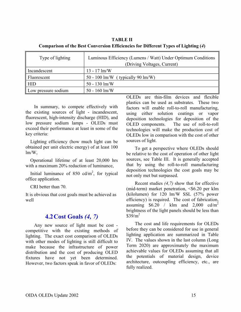
TABLE II Comparison of the Best Conversion Efficiencies for Different Types of Lighting (4)
Type of lighting Luminous Efficiency (Lumens / Watt) Under Optimum Conditions (Driving Voltages, Current)
Incandescent 13 - 17 lm/W Fluorescent 50 - 100 lm/W ( typically 90 lm/W) HID 50 - 130 lm/W Low pressure sodium 50 - 160 lm/W
In summary, to compete effectively with the existing sources of light - incandescent, fluorescent, high-intensity discharge (HID), and low pressure sodium lamps - OLEDs must exceed their performance at least in some of the key criteria:
Lighting efficiency (how much light can be obtained per unit electric energy) of at least 100 lm/W,
Operational lifetime of at least 20,000 hrs with a maximum 20% reduction of luminance,
Initial luminance of 850 cd/m2, for typical office application.
CRI better than 70.
It is obvious that cost goals must be achieved as well
4.2 Cost Goals (4, 7) Any new source of light must be cost -
competitive with the existing methods of lighting. The exact cost comparison of OLEDs with other modes of lighting is still difficult to make because the infrastructure of power distribution and the cost of producing OLED fixtures have not yet been determined. However, two factors speak in favor of OLEDs:
OLEDs are thin-film devices and flexible plastics can be used as substrates. These two factors will enable roll-to-roll manufacturing, using either solution coatings or vapor deposition technologies for deposition of the OLED components. The use of roll-to-roll technologies will make the production cost of OLEDs low in comparison with the cost of other sources of light.
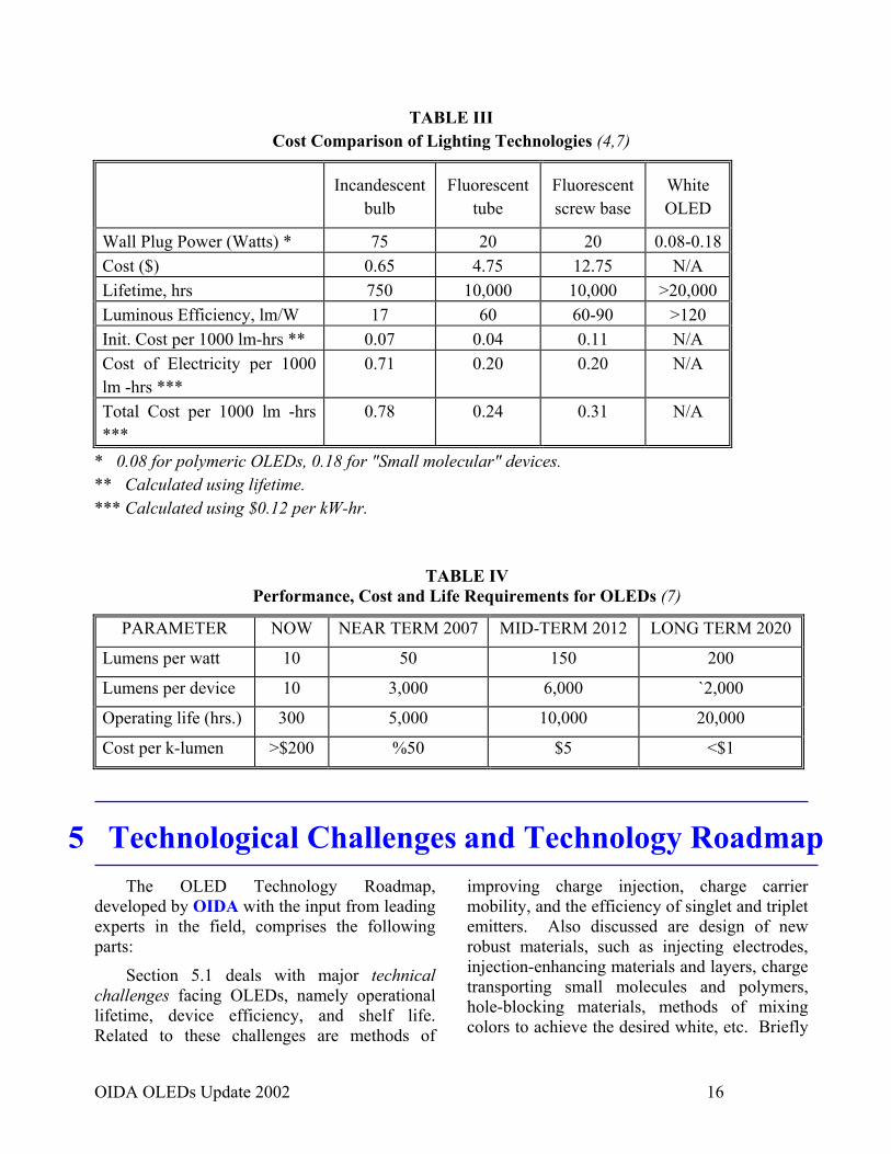
To get a perspective where OLEDs should be relative to the cost of operation of other light sources, see Table III. It is generally accepted that by using the roll-to-roll manufacturing deposition technologies the cost goals may be not only met but surpassed.
Recent studies (4,7) show that for effective (mid-term) market penetration, <$6.20 per klm (kilolumen) for 120 lm/W SSL (57% power efficiency) is required. The cost of fabrication, assuming $6.20 / klm and 2,000 cd/m2 brightness of the light panels should be less than $39/m2
The cost and life requirements for OLEDs before they can be considered for use in general lighting application are summarized in Table IV. The values shown in the last column (Long Term 2020) are approximately the maximum achievable values for OLEDs assuming that all the potentials of material design, device architecture, outcoupling efficiency, etc., are fully realized.
OIDA OLEDs Update 2002 16
TABLE III Cost Comparison of Lighting Technologies (4,7)
Incandescent
bulb Fluorescent
tube Fluorescent screw base
White OLED
Wall Plug Power (Watts) * 75 20 20 0.08-0.18Cost ($) 0.65 4.75 12.75 N/A Lifetime, hrs 750 10,000 10,000 >20,000 Luminous Efficiency, lm/W 17 60 60-90 >120 Init. Cost per 1000 lm-hrs ** 0.07 0.04 0.11 N/A Cost of Electricity per 1000 lm -hrs ***
0.71 0.20 0.20 N/A
Total Cost per 1000 lm -hrs ***
0.78 0.24 0.31 N/A
* 0.08 for polymeric OLEDs, 0.18 for "Small molecular" devices. ** Calculated using lifetime. *** Calculated using $0.12 per kW-hr.
TABLE IV
Performance, Cost and Life Requirements for OLEDs (7)
PARAMETER NOW NEAR TERM 2007 MID-TERM 2012 LONG TERM 2020
Lumens per watt 10 50 150 200
Lumens per device 10 3,000 6,000 `2,000
Operating life (hrs.) 300 5,000 10,000 20,000
Cost per k-lumen >$200 %50 $5 <$1
The OLED Technology Roadmap, developed by OIDA with the input from leading experts in the field, comprises the following parts:
Section 5.1 deals with major technical challenges facing OLEDs, namely operational lifetime, device efficiency, and shelf life. Related to these challenges are methods of
improving charge injection, charge carrier mobility, and the efficiency of singlet and triplet emitters. Also discussed are design of new robust materials, such as injecting electrodes, injection-enhancing materials and layers, charge transporting small molecules and polymers, hole-blocking materials, methods of mixing colors to achieve the desired white, etc. Briefly
5 Technological Challenges and Technology Roadmap
OIDA OLEDs Update 2002 17
discussed are also issues related to infrastructure, power supply and current distribution over large areas.
Section 5.2 deals with the manufacturing issues. While the roll-to-roll coating would be the most effective method of fabrication, many related issues have to be resolved such as differences in the methods of deposition of different materials and layers, protection against ambients (moisture and oxygen), and the availability of substrates.
Also, the conclusions of the Nov. 30 -Dec. 1, 2000 and April 5, 2002 workshops presented in Section 5 delineate the areas of research which has to be carried out to meet the efficiency and lifetime goals. These areas include the device photophysics to achieve higher efficiencies, understanding and control of the degradation processes which limit the device lifetime, materials research to design new better performing components, methods of protecting the device against the environment, etc.
The OIDA technology roadmap was developed jointly with the participants of the Nov. 30 through Dec. 1, 2000, and updated after the April 5, 2002 OLED workshops.
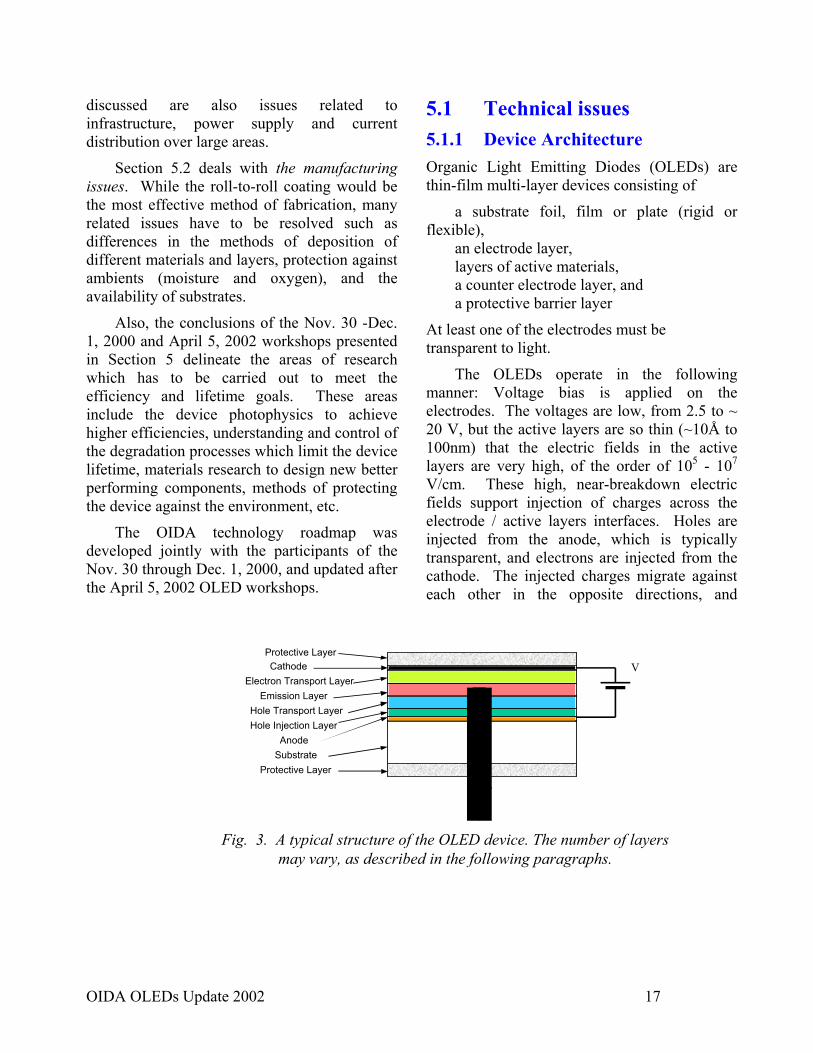
5.1 Technical issues 5.1.1 Device Architecture Organic Light Emitting Diodes (OLEDs) are thin-film multi-layer devices consisting of
a substrate foil, film or plate (rigid or flexible),
an electrode layer, layers of active materials, a counter electrode layer, and a protective barrier layer
At least one of the electrodes must be transparent to light.
The OLEDs operate in the following manner: Voltage bias is applied on the electrodes. The voltages are low, from 2.5 to ~ 20 V, but the active layers are so thin (~10Å to 100nm) that the electric fields in the active layers are very high, of the order of 105 - 107 V/cm. These high, near-breakdown electric fields support injection of charges across the electrode / active layers interfaces. Holes are injected from the anode, which is typically transparent, and electrons are injected from the cathode. The injected charges migrate against each other in the opposite directions, and
Protective LayerCathode
Electron Transport Layer
Hole Transport Layer
AnodeSubstrate
Protective Layer
Emission Layer
Hole Injection Layer
V
Fig. 3. A typical structure of the OLED device. The number of layers
may vary, as described in the following paragraphs.
OIDA OLEDs Update 2002 18
eventually meet and recombine. Recombination energy is released and the molecule or a polymer segment in which the recombination occurs, reaches an exited state. Excitons may migrate from molecule to molecule. Eventually, some molecules or a polymer segments release the energy as photons or heat. It is desirable that all the excess excitation energy is released as photons (light). The materials that are used to bring the charges to the recombination sites are usually, but not always, poor photon emitters (most of the excitation energy is released as heat). Therefore, suitable dopants are added, which first transfer the energy from the original excitons, and release the energy more efficiently as photons.
In OLEDs, approximately 25% of the excitons are in the singlet states and 75% in the triplet states (8). Emission of photons from the singlet states (fluorescence), in most cases facilitated by fluorescent dopants, was believed to be the only applicable form of energy release, thus limiting the internal quantum efficiency (IQE) of OLEDs to the maximum of 25%. Triplet states in organic materials were considered useless, since the energy of triplets was believed to dissipate non-radiatively, as heat. This low ratio of singlet states to the triplet states and, consequently, low device efficiency, would make the application of OLEDs as sources of light extremely difficult, if not unlikely. The utilization of the triplet states was virtually ignored until 1998 when researchers from University of Southern California, (USC) and Princeton University (PU) (9) demonstrated that by using phosphorescent dopants, the energy from all the triplet states could be harnessed as light (phosphorescence). The energy is transferred from the triplet excitons to the dopant molecules. However, not only excitons in the triplet states are utilized; these dopants, typically containing heavy atoms such as Ir or Pt, facilitate the forbidden "intersystem crossing" from the singlets to the triplet states, thus allowing for up to 100% IQE. In the recent
experiments, green- and red emitting phosphorescent OLEDs (PHOLEDS) show indeed nearly 100% IQE, and 19% external quantum efficiencies (EQE) (which, under the experimental conditions, translates to 40 lm/W).
This represents a quantum leap over the fluorescent systems (10, 11). The onset voltage, sometimes as low as 2.4 V is the voltage at which the current begins to flow and enough hole-electron pairs recombine to generate light visible by naked eye. The current and the corresponding light intensity increase with increasing the drive voltage.
Two types of materials are needed to bring the charges to the recombination sites: hole transport polymers or small molecules, and electron transport polymers or molecules. The energy mismatch between the electrode and the charge transport layer may require another layer to be sandwiched in between, to facilitate charge injection and thus to reduce the operating voltage. Some add a "buffer" layer, which may serve the same purpose (12).
Injection of holes is in most cases energetically easier than injection of electrons. This may result in the injection of excess of holes, which could drift to the cathode without meeting electrons. The excessive current would be wasteful and would heat the device. Usually, the electron transport layer acts as a hole blocker, but in some cases a hole-blocking layer is added between the electron and hole transport layers to prevent the escape of holes to the cathode. This has an additional benefit: the excess holes accumulate near the blocking layer and the resulting strong electric field across the cathode-electron transporter interface enhances injection of electrons to the system. This automatically balances the injection rates of both charge carriers, and maximizes recombination.
In some cases, exciton blocking layers are added to prevent excitons to reach the electrodes and decay non-radiatively. In other cases, a separate emission layer is sandwiched between
OIDA OLEDs Update 2002 19
the electron transport and hole transport layer. In white-color emitting devices there may be three separate emission layers, each emitting a different color. So today's devices may have a total of 7 - 9 layers - including electrodes, deposited by different techniques (sputtering, vapor deposition, solvent coating, etc). In spite of the large number of layers the total thickness of the device is typically less than 100 - 200 nm.
The deposition of all layers requires humidity- and oxygen-free conditions and all will require class 10 clean room. The cost consequence of such complexity is high. The deposition of each layer negatively impacts the manufacturing yield of the final device. The number of layers depends primarily on the type of materials used. It is still not clear how many layers will be ultimately needed to achieve the best performance.
Polymeric OLED devices Polymeric OLED devices have usually
fewer layers. The electroactive polymers may serve multiple functions: both electron and hole transport and light emission, even though dopant emitters can be used to tune the color. The electron transporting polymer and hole transporting polymer may be in one or two separate layers. In some cases, very thin layers of p-doped and n-doped semi-conducting polymers are sandwiched between the transport polymers and the cathode and anode, respectively, to facilitate charge injection. The active polymers and the injection layers are solution-coatable, but the electrodes are deposited by different techniques such as vapor deposition or ion sputtering, as in "small molecular" devices. To date, a large number of polymers have been synthesized and tested, and new structures are still emerging. The polymers have an extended chain of conjugated double bonds or aromatic rings, and pendant groups,
which determine the emission characteristics. The polymers are members of the polyphenylene vinylene family, polyfluorene homo- and copolymers and a new class of poly-spiro emitters (13).
"Small Molecular" OLED Devices
As the name indicates, the active components are "small" molecules. These small molecules are deposited by vapor deposition. Most "small molecules" would crystallize when deposited from solutions and crystallization would damage the device performance. Also, solution coating may result in uncontrollable mixing of layers. Most of the hole-transport small molecules contain one or several aromatic amine groups (a key pre-requisite for hole transport) and a variety of pendant substituents. These molecules have a low oxidation potential and must form stable cation-radicals.
Electron transport molecules are typically complexes of a metal such as aluminum (such as Alq3), boron, etc. with aromatic groups, bis-biphenyl anthracene, or, recently developed silacyclo-pentadienes (14, 15). These molecules have a relatively high electron affinity and must form stable anion-radicals. Some silacyclo-pentadiene may be unstable but new structures are being synthesized. The detailed description of the structures of charge transport materials is beyond the scope of this overview.
Also, there is a need to fabricate the devices with extremely uniform thicknesses of each layer. Nonuniformities may lead to localized surges of electric current, localized overheating, and gradual destruction of the device. The complexity makes the fabrication of OLEDs difficult and slows down testing of new materials.

OIDA OLEDs Update 2002 20
5.1.2 Operational Lifetime Insufficient lifetime presents special
challenges for OLEDs: high luminance levels, at least of the order of 850 cd/m2 with high conversion efficiency and sufficient operational stability (greater than 20,000 hrs of lifetime), must be achieved, and at these luminances, current OLEDs degrade rather quickly. The value of 850 cd/m2 was chosen as a first order goal because it is a luminance at which the viewer can still look comfortably into the light source, without glare. For many applications, either lower or higher luminances may be desirable. Currently, devices are much less efficient at these luminances than, for example, at 100 cd/m2.
At present, the OLED community defines the “end of life” as a point at which the luminance decays to 50% of the value at t = 0. This definition may be adequate for comparison purposes in research and development, but not for the general lighting applications. In displays, for example, the eye is sensitive to a 5% burn-in. Similar values are to be expected for distributed panel - like sources of illumination. Also, a customer should not be able to perceive the difference in light intensity and a shade of color between a new and an "aged" panel, if those two are placed next to each other. Therefore, for application to the
lighting industry, the definition of lifetime has yet to be developed.
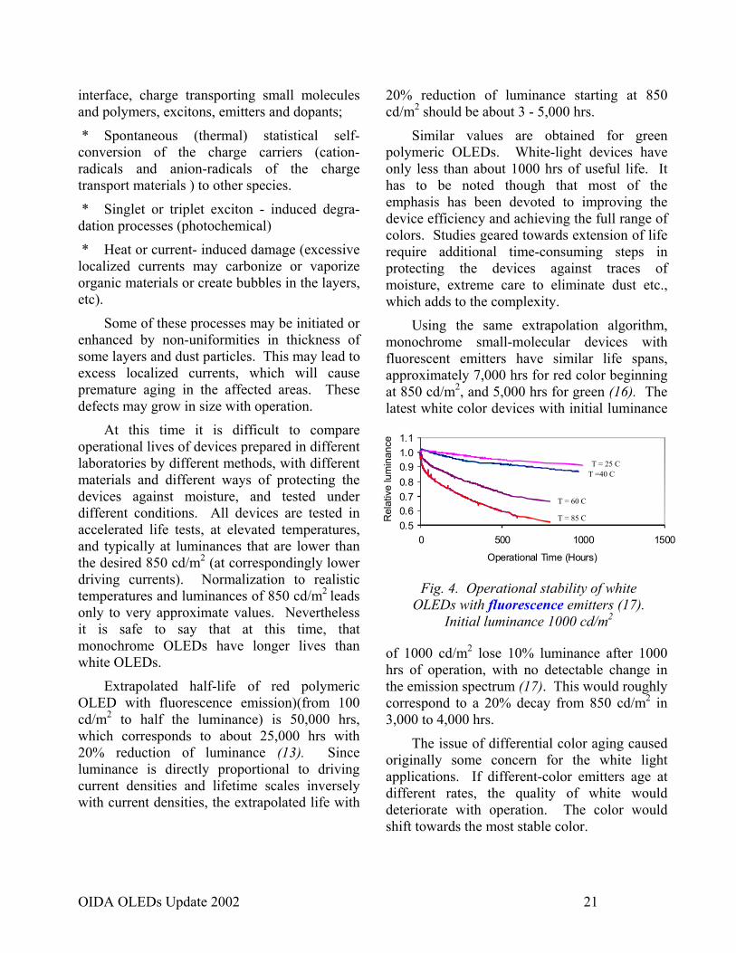
The OLED community generally agrees that the first level (somewhat arbitrary) target should be 20,000 hrs with a maximum 20% loss of luminance starting at 850 cd/m2.
The device luminance is directly proportional to the current density almost in the whole range of applicable currents. Experiments show that the lifetime is inversely proportional to the current density. In other words, the brighter the devices are, the shorter is their life. Degradation mechanisms leading to the decay of brightness are still not well understood. The degradation products from such thin films represent such tiny amounts of material that direct analytical study is conceptually difficult. Specific mechanisms are therefore not agreed upon. Also, there is no single cause that shortens the useful life of the OLED devices. Multiple degradation processes may occur simultaneously.
Among the factors that could reduce the device lifetime are:
* Chemical reactions of electrode materials, charge transporting small molecules and polymers, dopants and their excitons with the ambients (oxygen, CO2 and moisture)
* Electrochemical degradation (reduction or oxidation) involving the electrode-transport
Device Architecture - Summary:
There is a need to simplify the device architecture
* the number of layers should be reduced without compromising life and performance * simple, cost effective deposition processes must be developed * significant research in both the materials design and manufacturing technologies is needed to simplify the design of the device and the deposition processes * the uniformity requirements have to be quantified
OIDA OLEDs Update 2002 21
interface, charge transporting small molecules and polymers, excitons, emitters and dopants;
* Spontaneous (thermal) statistical self-conversion of the charge carriers (cation-radicals and anion-radicals of the charge transport materials ) to other species.
* Singlet or triplet exciton - induced degra-dation processes (photochemical)
* Heat or current- induced damage (excessive localized currents may carbonize or vaporize organic materials or create bubbles in the layers, etc).
Some of these processes may be initiated or enhanced by non-uniformities in thickness of some layers and dust particles. This may lead to excess localized currents, which will cause premature aging in the affected areas. These defects may grow in size with operation.
At this time it is difficult to compare operational lives of devices prepared in different laboratories by different methods, with different materials and different ways of protecting the devices against moisture, and tested under different conditions. All devices are tested in accelerated life tests, at elevated temperatures, and typically at luminances that are lower than the desired 850 cd/m2 (at correspondingly lower driving currents). Normalization to realistic temperatures and luminances of 850 cd/m2 leads only to very approximate values. Nevertheless it is safe to say that at this time, that monochrome OLEDs have longer lives than white OLEDs.
Extrapolated half-life of red polymeric OLED with fluorescence emission)(from 100 cd/m2 to half the luminance) is 50,000 hrs, which corresponds to about 25,000 hrs with 20% reduction of luminance (13). Since luminance is directly proportional to driving current densities and lifetime scales inversely with current densities, the extrapolated life with
20% reduction of luminance starting at 850 cd/m2 should be about 3 - 5,000 hrs.
Similar values are obtained for green polymeric OLEDs. White-light devices have only less than about 1000 hrs of useful life. It has to be noted though that most of the emphasis has been devoted to improving the device efficiency and achieving the full range of colors. Studies geared towards extension of life require additional time-consuming steps in protecting the devices against traces of moisture, extreme care to eliminate dust etc., which adds to the complexity.
Using the same extrapolation algorithm, monochrome small-molecular devices with fluorescent emitters have similar life spans, approximately 7,000 hrs for red color beginning at 850 cd/m2, and 5,000 hrs for green (16). The latest white color devices with initial luminance
of 1000 cd/m2 lose 10% luminance after 1000 hrs of operation, with no detectable change in the emission spectrum (17). This would roughly correspond to a 20% decay from 850 cd/m2 in 3,000 to 4,000 hrs.
The issue of differential color aging caused originally some concern for the white light applications. If different-color emitters age at different rates, the quality of white would deteriorate with operation. The color would shift towards the most stable color.
0.50.60.70.80.91.01.1
0 500 1000 1500
Operational Time (Hours)
Rel
ativ
e lu
min
ance
T = 25 CT =40 C
T = 60 C
T = 85 C
Fig. 4. Operational stability of white OLEDs with fluorescence emitters (17).
Initial luminance 1000 cd/m2
OIDA OLEDs Update 2002 22
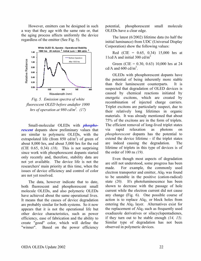
However, emitters can be designed in such a way that they age with the same rate or, that the aging process affects uniformly the device regardless of the emitter (See Fig. 5).
Small-molecular OLEDs with phospho-rescent dopants show preliminary values that are similar to polymeric OLEDs, with the extrapolated life (from 850 cd/m2) of green of about 8,000 hrs, and about 5,000 hrs for the red (CIE 0.65, 0.34) (18). This is not surprising since work with phosphorescent dopants started only recently and, therefore, stability data are not yet available. The device life is not the researchers' main priority at this time, when the issues of device efficiency and control of color are not yet resolved.
The data, however indicate that to date, both fluorescent and phosphorescent small molecule OLEDs, and also polymeric OLEDs have achieved about the same operational lives. It means that the causes of device degradation are probably similar for both systems. So it now appears that it is not the operational life but other device characteristics, such as power efficiency, ease of fabrication and the ability to create "good" color, which will define the "winner". Based on the power efficiency
potential, phosphorescent small molecule OLEDs have a clear edge.
The latest (6/2002) lifetime data (to half the initial luminance) from UDC (Universal Display Corporation) show the following values:
Red (CIE = 0.65, 0.34) 15,000 hrs at 11cd/A and initial 300 cd/m2
Green (CIE = 0.30, 0.63) 10,000 hrs at 24 cd/A and 600 cd/m2.
OLEDs with phosphorescent dopants have the potential of being inherently more stable than their luminescent counterparts. It is suspected that degradation of OLED devices is caused by chemical reactions initiated by energetic excitons, which are created by recombination of injected charge carriers. Triplet excitons are particularly suspect, due to their relatively long lifetimes in organic materials. It was already mentioned that about 75% of the excitons are in the form of triplets. The efficient removal of long-lived triplet states via rapid relaxation as photons on phosphorescent dopants has the potential to extend the device lifetime - if the triplet states are indeed causing the degradation. The lifetime of triplets in this type of devices is of the order of 100 ns (19).
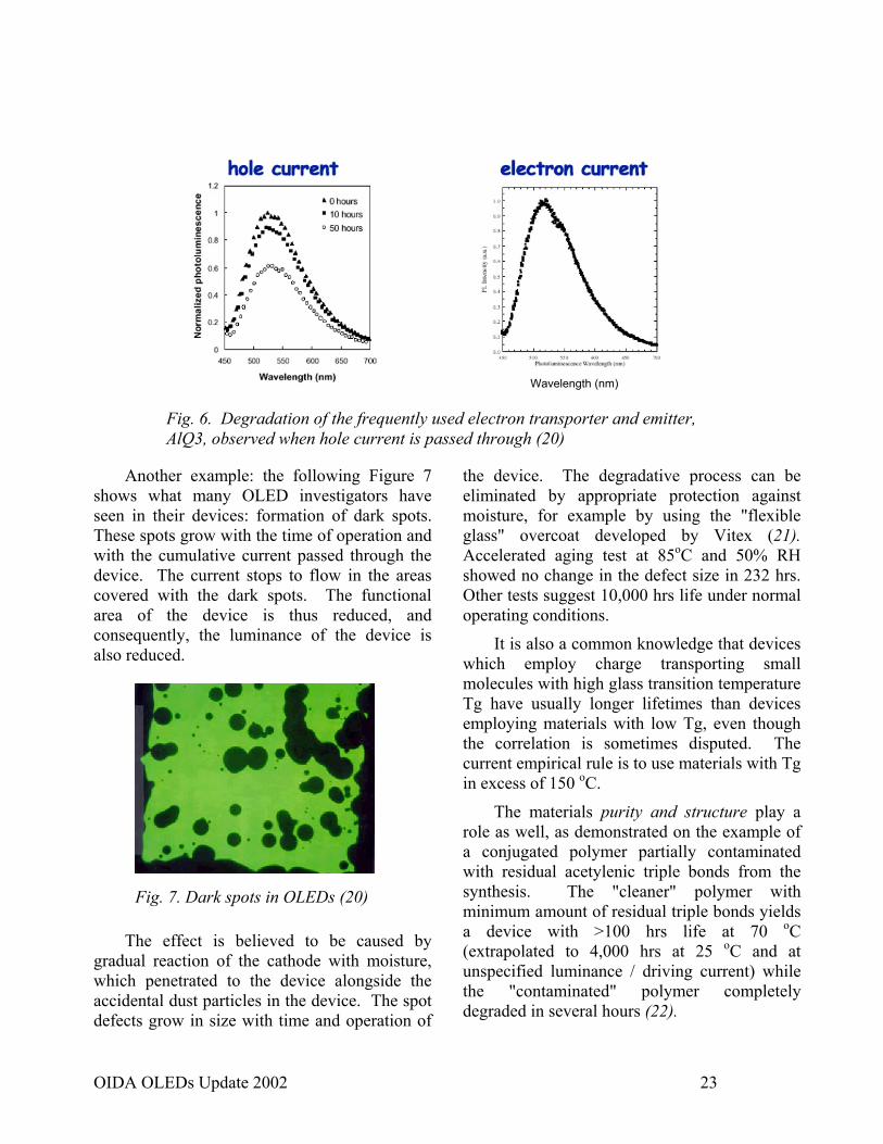
Even though most aspects of degradation are still not understood, some progress has been made. For example, the commonly used electron transporter and emitter, Alq3 was found to be unstable in the positive (cation-radical) state (20). It's photoluminescence has been shown to decrease with the passage of hole current while the electron current did not cause any change (Fig. 6). One possible course of action is to replace Alq3, or block holes from entering the Alq3 layer. Alternatives exist for the replacement of Alq3 such as frequently used oxadiazole derivatives or silacyclopentadienes, if they turn out to be stable enough (14, 15). Similar type of degradation has not been observed in polymeric devices.
White OLED EL Spectra - Operational Stability 1000 hrs 20 mA/cm 2 Initial Lum ~ 980 cd/m 2
0.00
0.20
0.40
0.60
0.80
1.00
1.20
1.40
0 500 600 700 800
Before Operation
After 100 0 hrs
Wavelength (nm)
Rel
ativ
e R
adia
nce
Fig. 5. Emission spectra of white fluorescent OLED before andafter 1000
hrs of operation at 980 cd/m2. (17)
OIDA OLEDs Update 2002 23
Another example: the following Figure 7 shows what many OLED investigators have seen in their devices: formation of dark spots. These spots grow with the time of operation and with the cumulative current passed through the device. The current stops to flow in the areas covered with the dark spots. The functional area of the device is thus reduced, and consequently, the luminance of the device is also reduced.
The effect is believed to be caused by gradual reaction of the cathode with moisture, which penetrated to the device alongside the accidental dust particles in the device. The spot defects grow in size with time and operation of
the device. The degradative process can be eliminated by appropriate protection against moisture, for example by using the "flexible glass" overcoat developed by Vitex (21). Accelerated aging test at 85oC and 50% RH showed no change in the defect size in 232 hrs. Other tests suggest 10,000 hrs life under normal operating conditions.
It is also a common knowledge that devices which employ charge transporting small molecules with high glass transition temperature Tg have usually longer lifetimes than devices employing materials with low Tg, even though the correlation is sometimes disputed. The current empirical rule is to use materials with Tg in excess of 150 oC.
The materials purity and structure play a role as well, as demonstrated on the example of a conjugated polymer partially contaminated with residual acetylenic triple bonds from the synthesis. The "cleaner" polymer with minimum amount of residual triple bonds yields a device with >100 hrs life at 70 oC (extrapolated to 4,000 hrs at 25 oC and at unspecified luminance / driving current) while the "contaminated" polymer completely degraded in several hours (22).
Fig. 6. Degradation of the frequently used electron transporter and emitter, AlQ3, observed when hole current is passed through (20)
Wavelength (nm)
Fig. 7. Dark spots in OLEDs (20)
OIDA OLEDs Update 2002 24
Other possible causes of degradation of OLEDs are variously attributed to electro-migration of cathodes due to localized short circuits, photodegradation in the presence of oxygen, possibly involving the triplet excitons, electrochemical reactions at the interfaces, and general instabilities of the molecules in the oxidized (cation-radical) or reduced (anion-radical) states. These short-comings will be mitigated by the appropriate design of the charge transport small molecules, by the treatments of electrodes and by the development of better encapsulation methods to prevent the access of oxygen and moisture.
At this time, it appears that the major cause of degradation is the presence of moisture. It also appears that the currently used plastic substrates of the Mylar type are so permeable to moisture and oxygen to the point that the devices are gradually destroyed by water molecules that diffuse through the layer. As the methods of encapsulation and fabrication under humidity-free and anaerobic conditions improve, the useful life of OLEDs is expected to increase considerably.
A new technique has already been developed to protect OLEDs on plastic substrates (23). It involves a deposition of a transparent flexible multi-layer organic-
inorganic thin film barrier on top of the plastic using a hybrid process of cryo-condensation and polymerization of an organic monomer precursor followed by vapor deposition of a nanoscale barrier layer. This multi-layer hybrid barrier restricts permeation of both oxygen and moisture to non-measurable levels while retaining flexibility and transparency of the substrate. Residual permeation is due to pinholes rather than bulk diffusion. At least 10,000 hrs. of useful life of OLEDs are projected using this method of encapsulation.
For small display devices, the lifetimes of all colors (> 5,000 hours at 100 cd/m2) are sufficient. For lighting applications, these values are inadequate. An extension of life of white by a factor of 20-50 from the current values is needed to reach parity with fluorescent lighting. In view of the recent progress with encapsulation and with better understanding of the degradation processes, this is achievable.
One of the major manufacturing problems will be maintaining the uniformity of the layers. Any localized reductions of the thickness will result in increased electric fields, larger currents, and potentially more damage. This will be a particularly challenging issue, given the dimension of the layers (the thicknesses are of the order of 2 - 40 nm).
Operational Lifetime - Summary:
Understanding of the following issues must be acquired to improve the operation life of OLEDs:
* Degradation mechanisms * Elucidation of the role of triplet and singlet excitons in the degradation processes * Effect of Tg and morphology of the active materials * The role of structural impurities in active polymers in polymeric OLEDs * The possibility of electrochemical reactions at the interfaces * The causes of physical defects (bubbles, "dark spots" etc.) * The methods of encapsulation and other means of protection against the ambients * Design of charge transport materials with stable cation- or anion-radicals
OIDA OLEDs Update 2002 25
5.1.3. Device Efficiency The efficiency of OLEDs can be
characterized by its quantum efficiency, power efficiency (lm/W), luminous efficiency (cd/A), sometimes called luminous yield.
The device quantum efficiency ηq has two parts: internal and external:
Internal quantum efficiency ηint or IQE, is the number of photons generated inside the device per number of injected hole - electron pairs. A large fraction of generated photons stays trapped and absorbed inside the device.
External quantum efficiency ηext or EQE, is the number of photons released from the device per number of injected hole - electron pairs.
Luminous (Power) efficiency ηp is the ratio of the lumen output to the input electrical watts (lm/W).
Luminous efficacy ην represents the ratio of the lumen output to the optical watts (radiative power) (24). The luminous efficiency and luminous efficacy of a device account for a spectral sensitivity of a human eye. Therefore, two devices with similar quantum efficiencies can have different luminous performance, depending on the spectrum of the emitted light. In the process of converting electrical power into optical power, losses are incurred due to non-radiative processes (thermal relaxation of excitons, internal reflection and absorption of photons). The luminous efficiency and luminous efficacy are related as
ηp = ην (Pin / Φ)
where Pin is input el. watts, and Φ is lumen output.
Candela (cd) is a unit of luminous intensity and defined as such a value that the luminous intensity of a full radiator at the solidification temperature of platinum is 60 candelas per square centimeter.
1 Lumen (lm) is a unit of luminous flux and is defined as the luminous flux emitted in a solid angle of one steradian by a uniform point source of intensity of 1 candela.
1 lm = 1 cd x steradian
One steradian (sr) is defined as the solid angle (Ω) subtended at the vertex by a spherical sector whose spherical part (S) of the surface is equal to the square of the radius of the sphere R:
Example: If a source of luminous intensity 1 cd radiates normally upon a spherical surface of area 1m2 at a distance of 1 m from the source, the luminous flux thus emitted is 1 lm.
Internal Quantum Efficiency
For OLEDs which use fluorescence emitters,
ηint = IQE = γ ηs Φf
where γ is the charge balance factor (a fraction of injected charges that produce excitons), ηs is the singlet excitation efficiency (the fraction of excitons that are formed as singlets), and Φf is the quantum efficiency of fluorescence (the fraction of energy released from the fluorescent material as light). Based on spin statistics, the singlet excitation efficiency ηs was believed to have a maximum value of 25%. In other words, only 25% of excitons were supposed to be singlets, which may be capable of relaxing the energy as photons. Until recently, this was thought to impose a 25% fundamental limit on
OIDA OLEDs Update 2002 26
the internal quantum efficiency of all OLEDs. However, recent studies seem to indicate that this “law” may no longer be valid; singlet excitation efficiencies higher than 25% have been identified in polymeric OLEDs (25) but only at very low temperatures. However, this finding has not yet been supported by higher OLED device efficiency.
The quantum efficiency of fluorescence Φf can approach unity, but only in dilute solutions. General problem is to maintain high Φf in solid state. In reality, few materials have Φf greater than 50% in OLEDs. Sometimes, greater efficiency of fluorescence in small- molecular devices is achieved by adding dopants, for example quinacridone to the host Alq3. Again, further progress can be expected in raising the efficiency of fluorescence. For example, recent study shows that a novel electron transporting material, which is also a good blue-green emitter, 1,2-bis(1-methyl-2,3,4,5-tetraphenyl-silacyclopentadienyl)ethane, exhibits solid state fluorescence with an absolute quantum yield of 97% (14). This shows that a rational molecular design can generate materials for fluorescent OLED devices with near 25 % IQE. However, this particular compound may be unstable; lifetime of OLEDs containing this new material has not yet been tested.
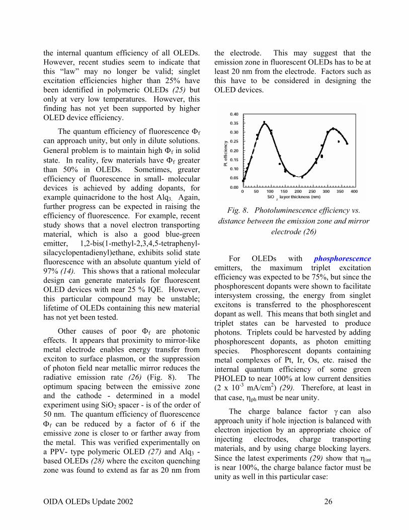
Other causes of poor Φf are photonic effects. It appears that proximity to mirror-like metal electrode enables energy transfer from exciton to surface plasmon, or the suppression of photon field near metallic mirror reduces the radiative emission rate (26) (Fig. 8). The optimum spacing between the emissive zone and the cathode - determined in a model experiment using SiO2 spacer - is of the order of 50 nm. The quantum efficiency of fluorescence Φf can be reduced by a factor of 6 if the emissive zone is closer to or farther away from the metal. This was verified experimentally on a PPV- type polymeric OLED (27) and Alq3 - based OLEDs (28) where the exciton quenching zone was found to extend as far as 20 nm from
the electrode. This may suggest that the emission zone in fluorescent OLEDs has to be at least 20 nm from the electrode. Factors such as this have to be considered in designing the OLED devices.
For OLEDs with phosphorescence emitters, the maximum triplet excitation efficiency was expected to be 75%, but since the phosphorescent dopants were shown to facilitate intersystem crossing, the energy from singlet excitons is transferred to the phosphorescent dopant as well. This means that both singlet and triplet states can be harvested to produce photons. Triplets could be harvested by adding phosphorescent dopants, as photon emitting species. Phosphorescent dopants containing metal complexes of Pt, Ir, Os, etc. raised the internal quantum efficiency of some green PHOLED to near 100% at low current densities (2 x 10⁻³ mA/cm2) (29). Therefore, at least in that case, ηph must be near unity.
The charge balance factor γ can also approach unity if hole injection is balanced with electron injection by an appropriate choice of injecting electrodes, charge transporting materials, and by using charge blocking layers. Since the latest experiments (29) show that ηint is near 100%, the charge balance factor must be unity as well in this particular case:
Fig. 8. Photoluminescence efficiency vs. distance between the emission zone and mirror
electrode (26)
OIDA OLEDs Update 2002 27
ηint = IQE = γ ηph Φp = γ = 100%
Among the fundamental phenomena that can also lead to a reduced internal efficiency are
* exciton-exciton quenching (30)
T1 + T1 S1 + So
* Polaron - exciton quenching (31)
S1 or T1 So
* Exciton dissociation (32)
S1 or T1 X+ + X-
Some of these exciton annihilation mechanisms are common to both fluorescent and phosphorescent systems. Understanding and control of these phenomena will lead to increased internal efficiencies.
The efficiency–vs.–current characteristics of phosphorescent organic light-emitting diodes (PHOLED ™ ) devices have been studied and compared to fluorescent polymer LEDs (POLED) and fluorescent small-molecule organic light-emitting diodes (SMOLED). Results show that (UDC) proprietary phosphorescent OLEDs (PHOLEDs™) have indeed significantly higher efficiency than polymeric OLEDs (PLEDs) and SMOLEDs with fluorescent emitters in both the low- and high-current regimes. (33)
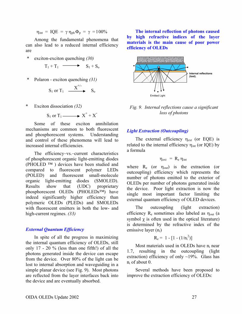
External Quantum Efficiency
In spite of all the progress in maximizing the internal quantum efficiency of OLEDs, still only 17 - 20 % (less than one fifth!) of all the photons generated inside the device can escape from the device. Over 80% of the light can be lost to internal absorption and waveguiding in a simple planar device (see Fig. 9). Most photons are reflected from the layer interfaces back into the device and are eventually absorbed.
The internal reflection of photons caused by high refractive indices of the layer materials is the main cause of poor power efficiency of OLEDs
Light Extraction (Outcoupling)
The external efficiency ηext (or EQE) is related to the internal efficiency ηint (or IQE) by a formula
ηext = Re ηint
where Re (or ηout) is the extraction (or outcoupling) efficiency which represents the number of photons emitted to the exterior of OLEDs per number of photons generated inside the device. Poor light extraction is now the single most important factor limiting the external quantum efficiency of OLED devices.
The outcoupling (light extraction) efficiency Re sometimes also labeled as ηout (a symbol χ is often used in the optical literature) is determined by the refractive index of the emissive layer (ni)
Re = 1 - [1 - (1/ni2)]
Most materials used in OLEDs have ni near 1.7, resulting in the outcoupling (light extraction) efficiency of only ~19%. Glass has ni of about 0.
Several methods have been proposed to improve the extraction efficiency of OLEDs:
X+/- Emitted Light
Internal reflections (lost).
Fig. 9. Internal reflections cause a significant loss of photons
OIDA OLEDs Update 2002 28
Surface texturing - gives the photons multiple opportunities to reflect and eventually find the escape cone. Even though the surface texturing experiments have begun only recently, a factor of 2 improvement in Re has already been achieved. (34).
Substrate modification by index matching. or using low-refractive index substrates. An improvement of Re (or ηout) by a factor of 2.5 has already been reported (35).
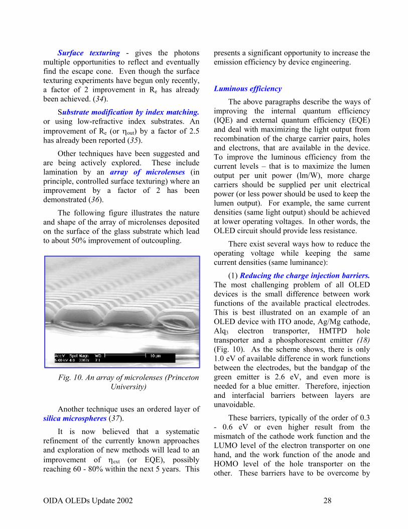
Other techniques have been suggested and are being actively explored. These include lamination by an array of microlenses (in principle, controlled surface texturing) where an improvement by a factor of 2 has been demonstrated (36).
The following figure illustrates the nature and shape of the array of microlenses deposited on the surface of the glass substrate which lead to about 50% improvement of outcoupling.
Fig. 10. An array of microlenses (Princeton University)
Another technique uses an ordered layer of silica microspheres (37).
It is now believed that a systematic refinement of the currently known approaches and exploration of new methods will lead to an improvement of ηext (or EQE), possibly reaching 60 - 80% within the next 5 years. This
presents a significant opportunity to increase the emission efficiency by device engineering.
Luminous efficiency The above paragraphs describe the ways of
improving the internal quantum efficiency (IQE) and external quantum efficiency (EQE) and deal with maximizing the light output from recombination of the charge carrier pairs, holes and electrons, that are available in the device. To improve the luminous efficiency from the current levels – that is to maximize the lumen output per unit power (lm/W), more charge carriers should be supplied per unit electrical power (or less power should be used to keep the lumen output). For example, the same current densities (same light output) should be achieved at lower operating voltages. In other words, the OLED circuit should provide less resistance.
There exist several ways how to reduce the operating voltage while keeping the same current densities (same luminance):
(1) Reducing the charge injection barriers. The most challenging problem of all OLED devices is the small difference between work functions of the available practical electrodes. This is best illustrated on an example of an OLED device with ITO anode, Ag/Mg cathode, Alq3 electron transporter, HMTPD hole transporter and a phosphorescent emitter (18) (Fig. 10). As the scheme shows, there is only 1.0 eV of available difference in work functions between the electrodes, but the bandgap of the green emitter is 2.6 eV, and even more is needed for a blue emitter. Therefore, injection and interfacial barriers between layers are unavoidable.
These barriers, typically of the order of 0.3 - 0.6 eV or even higher result from the mismatch of the cathode work function and the LUMO level of the electron transporter on one hand, and the work function of the anode and HOMO level of the hole transporter on the other. These barriers have to be overcome by
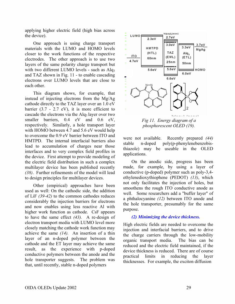
OIDA OLEDs Update 2002 29
applying higher electric field (high bias across the device).
One approach is using charge transport materials with the LUMO and HOMO levels closer to the work functions of the respective electrodes. The other approach is to use two layers of the same polarity charge transport but with two different LUMO levels - such as Alq3 and TAZ shown in Fig. 11 - to enable cascading electrons over LUMO levels that are close to each other.
This diagram shows, for example, that instead of injecting electrons from the Mg/Ag cathode directly to the TAZ layer over an 1.0 eV barrier (3.7 - 2.7 eV), it is more efficient to cascade the electrons via the Alq3 layer over two smaller barriers, 0.4 eV and 0.6 eV, respectively. Similarly, a hole transport layer with HOMO between 4.7 and 5.6 eV would help to overcome the 0.9 eV barrier between ITO and HMTPD. The internal interfacial barriers also lead to accumulation of charges near those interfaces and to very complex field profiles in the device. First attempt to provide modeling of the electric field distribution in such a complex multilayer device has been published recently (38). Further refinements of the model will lead to design principles for multilayer devices.
Other (empirical) approaches have been used as well: On the cathodic side, the addition of LiF (39-42) to the common cathodes reduces considerably the injection barriers for electrons and now enables using less reactive Al with higher work function as cathode. CsF appears to have the same effect (43). A re-design of electron transport media with LUMO level more closely matching the cathode work function may achieve the same (14). An insertion of a thin layer of an n-doped polymer between the cathode and the ET layer may achieve the same result, as the experience with p-doped conductive polymers between the anode and the hole transporter suggests. The problem was that, until recently, stable n-doped polymers
were not available. Recently prepared (44) stable n-doped poly(p-phenylenebenzobis-thiazole) may be useable in the OLED applications.
On the anodic side, progress has been made, for example, by using a layer of conductive (p-doped) polymer such as poly-3,4-ethylenedioxythiophene (PEDOT) (13), which not only facilitates the injection of holes, but smoothens the rough ITO conductive anode as well. Some researchers add a "buffer layer" of a phthalocyanine (12) between ITO anode and the hole transporter, presumably for the same purpose.
(2) Minimizing the device thickness. High electric fields are needed to overcome the injection and interfacial barriers, and to drive the charge carriers through the low-mobility organic transport media. The bias can be reduced and the electric field maintained, if the device thickness is reduced. There are of course practical limits in reducing the layer thicknesses. For example, the exciton diffusion
Fig 11. Energy diagram of a phosphorescent OLED (19).
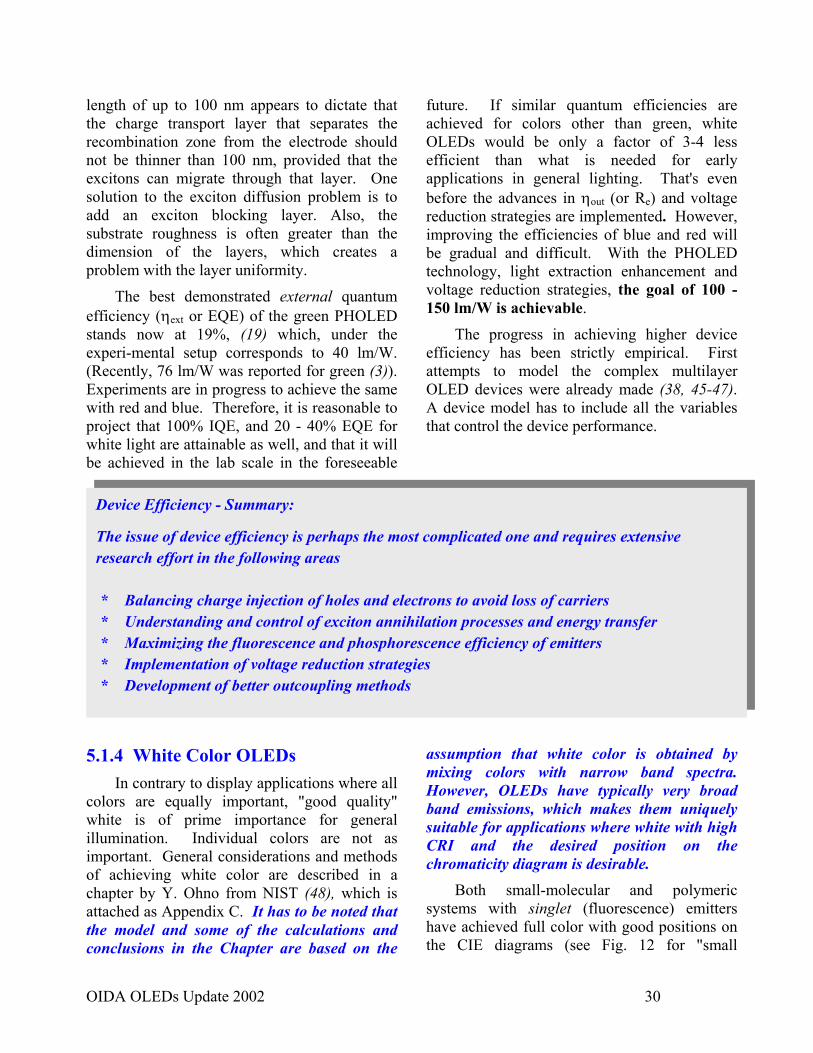
OIDA OLEDs Update 2002 30
length of up to 100 nm appears to dictate that the charge transport layer that separates the recombination zone from the electrode should not be thinner than 100 nm, provided that the excitons can migrate through that layer. One solution to the exciton diffusion problem is to add an exciton blocking layer. Also, the substrate roughness is often greater than the dimension of the layers, which creates a problem with the layer uniformity.
The best demonstrated external quantum efficiency (ηext or EQE) of the green PHOLED stands now at 19%, (19) which, under the experi-mental setup corresponds to 40 lm/W. (Recently, 76 lm/W was reported for green (3)). Experiments are in progress to achieve the same with red and blue. Therefore, it is reasonable to project that 100% IQE, and 20 - 40% EQE for white light are attainable as well, and that it will be achieved in the lab scale in the foreseeable
future. If similar quantum efficiencies are achieved for colors other than green, white OLEDs would be only a factor of 3-4 less efficient than what is needed for early applications in general lighting. That's even before the advances in ηout (or Re) and voltage reduction strategies are implemented. However, improving the efficiencies of blue and red will be gradual and difficult. With the PHOLED technology, light extraction enhancement and voltage reduction strategies, the goal of 100 - 150 lm/W is achievable.
The progress in achieving higher device efficiency has been strictly empirical. First attempts to model the complex multilayer OLED devices were already made (38, 45-47). A device model has to include all the variables that control the device performance.
5.1.4 White Color OLEDs In contrary to display applications where all
colors are equally important, "good quality" white is of prime importance for general illumination. Individual colors are not as important. General considerations and methods of achieving white color are described in a chapter by Y. Ohno from NIST (48), which is attached as Appendix C. It has to be noted that the model and some of the calculations and conclusions in the Chapter are based on the
assumption that white color is obtained by mixing colors with narrow band spectra. However, OLEDs have typically very broad band emissions, which makes them uniquely suitable for applications where white with high CRI and the desired position on the chromaticity diagram is desirable.
Both small-molecular and polymeric systems with singlet (fluorescence) emitters have achieved full color with good positions on the CIE diagrams (see Fig. 12 for "small
Device Efficiency - Summary:
The issue of device efficiency is perhaps the most complicated one and requires extensive research effort in the following areas * Balancing charge injection of holes and electrons to avoid loss of carriers * Understanding and control of exciton annihilation processes and energy transfer * Maximizing the fluorescence and phosphorescence efficiency of emitters * Implementation of voltage reduction strategies * Development of better outcoupling methods
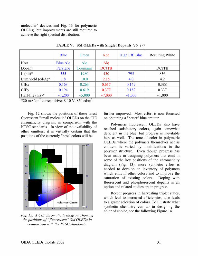
OIDA OLEDs Update 2002 31
molecular" devices and Fig. 13 for polymeric OLEDs), but improvements are still required to achieve the right spectral distribution.
TABLE V. SM OLEDs with Singlet Dopants (16, 17)
Blue Green Red High Eff. Blue Resulting White
Host Blue Alq Alq Alq Dopant Perylene Coumarin DCJTB DCJTB L (nit)* 355 1980 430 795 836 Lum.yield (cd/A)* 1.8 10.0 2.15 4.0 4.2 CIEx 0.163 0.263 0.617 0.149 0.388 CIEy 0.194 0.619 0.377 0.182 0.337 Half-life (hrs)* ~1,200 ~5,000 ~7,000 ~1,000 ~1,000 *20 mA/cm2 current drive; 8-10 V, 850 cd/m2.
Fig. 12 shows the positions of these latest fluorescent "small molecule" OLEDs on the CIE chromaticity diagram, in comparison with the NTSC standards. In view of the availability of other emitters, it is virtually certain that the positions of the currently "best" colors will be
further improved. Most effort is now focussed on obtaining a "better" blue emitter.
Polymeric fluorescent OLEDs also have reached satisfactory colors, again somewhat deficient in the blue, but progress is inevitable here as well. The tone of color in polymeric OLEDs where the polymers themselves act as emitters is varied by modifications in the polymer structure. Even though progress has been made in designing polymers that emit in some of the key positions of the chromaticity diagram (Fig. 13), more synthetic effort is needed to develop an inventory of polymers which emit in other colors and to improve the saturation of existing colors. Doping with fluorescent and phosphorescent dopants is an option and related studies are in progress.
Recent progress in harvesting triplet states, which lead to increased efficiencies, also leads to a grater selection of colors. To illustrate what synthetic chemistry can do in designing the color of choice, see the following Figure 14.
Fig. 12. A CIE chromaticity diagram showing the positions of “fluorescent” SM OLEDs in
comparison with the NTSC standards.
NTSC Green(0.21,0.71)
NTSC Red(0.67,0.33)
NTSC Blue(0.14,0.08
)
OELD Green(0.30,0.63)
OELD Blue(0.17,0.17)
OELD Red(0.65,0.34)
color coordinate
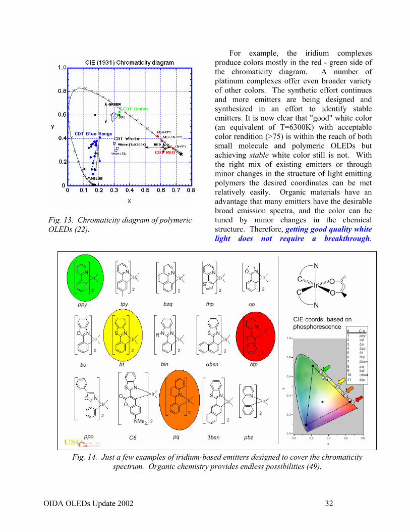
OIDA OLEDs Update 2002 32
For example, the iridium complexes produce colors mostly in the red - green side of the chromaticity diagram. A number of platinum complexes offer even broader variety of other colors. The synthetic effort continues and more emitters are being designed and synthesized in an effort to identify stable emitters. It is now clear that "good" white color (an equivalent of T=6300K) with acceptable color rendition (>75) is within the reach of both small molecule and polymeric OLEDs but achieving stable white color still is not. With the right mix of existing emitters or through minor changes in the structure of light emitting polymers the desired coordinates can be met relatively easily. Organic materials have an advantage that many emitters have the desirable broad emission spcctra, and the color can be tuned by minor changes in the chemical structure. Therefore, getting good quality white light does not require a breakthrough.
Fig. 13. Chromaticity diagram of polymeric OLEDs (22).
Fig. 14. Just a few examples of iridium-based emitters designed to cover the chromaticity spectrum. Organic chemistry provides endless possibilities (49).
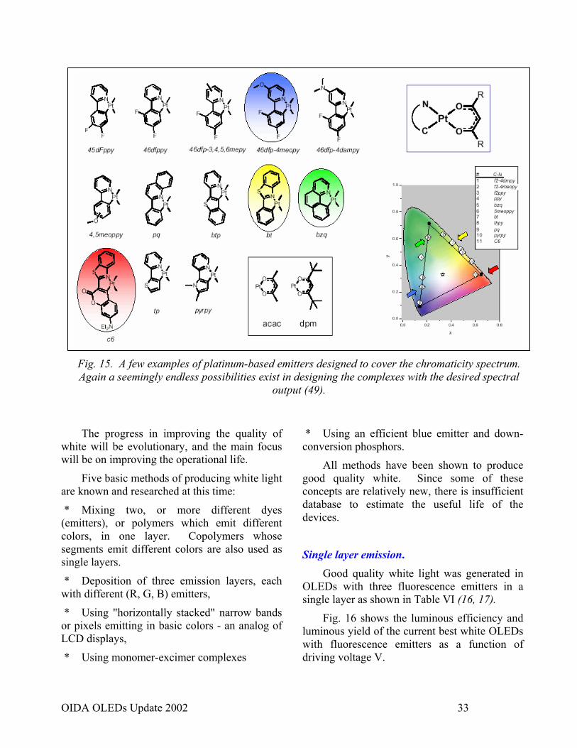
OIDA OLEDs Update 2002 33
The progress in improving the quality of white will be evolutionary, and the main focus will be on improving the operational life.
Five basic methods of producing white light are known and researched at this time:
* Mixing two, or more different dyes (emitters), or polymers which emit different colors, in one layer. Copolymers whose segments emit different colors are also used as single layers.
* Deposition of three emission layers, each with different (R, G, B) emitters,
* Using "horizontally stacked" narrow bands or pixels emitting in basic colors - an analog of LCD displays,
* Using monomer-excimer complexes
* Using an efficient blue emitter and down-conversion phosphors.
All methods have been shown to produce good quality white. Since some of these concepts are relatively new, there is insufficient database to estimate the useful life of the devices.
Single layer emission. Good quality white light was generated in
OLEDs with three fluorescence emitters in a single layer as shown in Table VI (16, 17).
Fig. 16 shows the luminous efficiency and luminous yield of the current best white OLEDs with fluorescence emitters as a function of driving voltage V.
Fig. 15. A few examples of platinum-based emitters designed to cover the chromaticity spectrum. Again a seemingly endless possibilities exist in designing the complexes with the desired spectral
output (49).
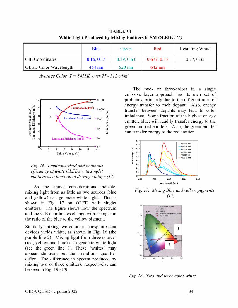
OIDA OLEDs Update 2002 34
TABLE VI White Light Produced by Mixing Emitters in SM OLEDs (16)
Blue Green Red Resulting White
CIE Coordinates 0.16, 0.15 0.29, 0.63 0.677, 0.33 0.27, 0.35
OLED Color Wavelength 454 nm 520 nm 642 nm
Average Color T = 8413K over 27 - 512 cd/m2
As the above considerations indicate, mixing light from as little as two sources (blue and yellow) can generate white light. This is shown in Fig. 17 on OLED with singlet emitters. The figure shows how the spectrum and the CIE coordinates change with changes in the ratio of the blue to the yellow pigment.
Similarly, mixing two colors in phosphorescent devices yields white, as shown in Fig. 16 (the purple line 2). Mixing light from three sources (red, yellow and blue) also generate white light (see the green line 3). These "whites" may appear identical, but their rendition qualities differ. The difference in spectra produced by mixing two or three emitters, respectively, can be seen in Fig. 19 (50).
The two- or three-colors in a single emissive layer approach has its own set of problems, primarily due to the different rates of energy transfer to each dopant. Also, energy transfer between dopants may lead to color imbalance. Some fraction of the highest-energy emitter, blue, will readily transfer energy to the green and red emitters. Also, the green emitter can transfer energy to the red emitter.
Fig. 17. Mixing Blue and yellow pigments (17)
0
2
4
6
8
10
12
0 2 4 6 8 10 12 14Drive Voltage (V)
Lum
inou
s Yie
ld (c
d/A
) L
umin
ous E
ffic
ienc
y (lm
/W)
0.1
1.0
10
100
1,000 .
10,000
Luminous Efficiency (lm/W)
Luminous Yield (cd/A)
Luminance (cd/m2)Lu
min
ance
(cd/
m2)
Fig. 16. Luminous yield and luminous efficiency of white OLEDs with singlet emitters as a function of driving voltage (17) 0.0
0.5
1.0
1.5
2.0
2.5
3.0
3.5
4.0
4.5
400 500 600 700 800Wavelength (nm)
Rad
ianc
e (a
.u.)
CIE 0.17, 0.25
CIE 0.25, 0.32
CIE 0.27, 0.34
CIE 0.33, 0.39CIE 038, 0.42
CIE 0.42, 0.44
2
3
Fig .18. Two-and three color white
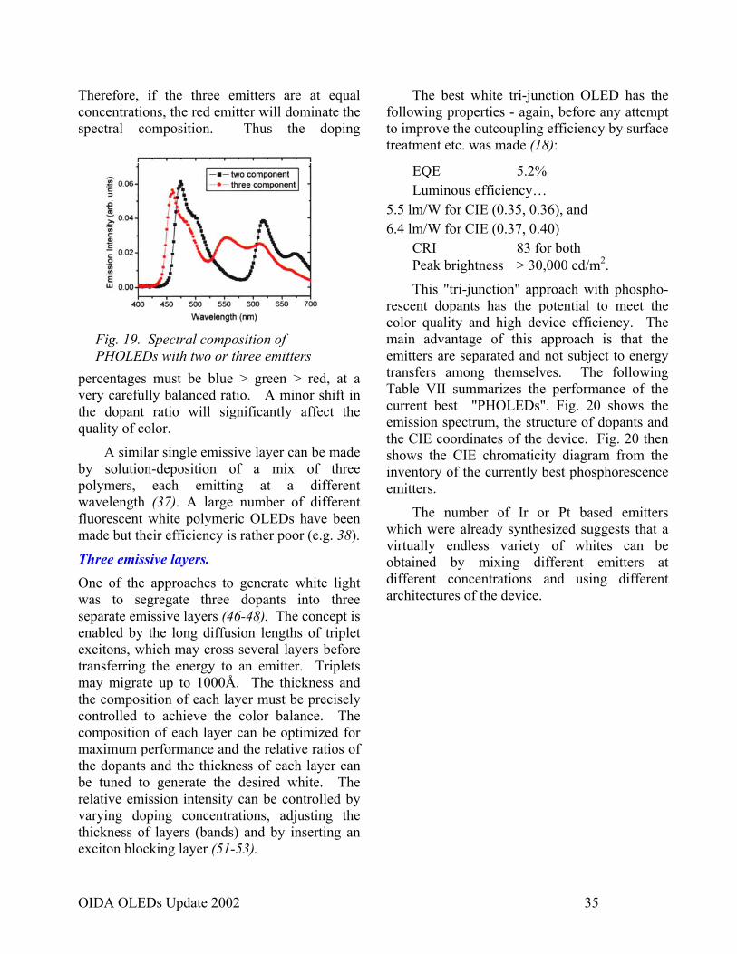
OIDA OLEDs Update 2002 35
Therefore, if the three emitters are at equal concentrations, the red emitter will dominate the spectral composition. Thus the doping
percentages must be blue > green > red, at a very carefully balanced ratio. A minor shift in the dopant ratio will significantly affect the quality of color.
A similar single emissive layer can be made by solution-deposition of a mix of three polymers, each emitting at a different wavelength (37). A large number of different fluorescent white polymeric OLEDs have been made but their efficiency is rather poor (e.g. 38).
Three emissive layers. One of the approaches to generate white light was to segregate three dopants into three separate emissive layers (46-48). The concept is enabled by the long diffusion lengths of triplet excitons, which may cross several layers before transferring the energy to an emitter. Triplets may migrate up to 1000Å. The thickness and the composition of each layer must be precisely controlled to achieve the color balance. The composition of each layer can be optimized for maximum performance and the relative ratios of the dopants and the thickness of each layer can be tuned to generate the desired white. The relative emission intensity can be controlled by varying doping concentrations, adjusting the thickness of layers (bands) and by inserting an exciton blocking layer (51-53).
The best white tri-junction OLED has the following properties - again, before any attempt to improve the outcoupling efficiency by surface treatment etc. was made (18):
EQE 5.2% Luminous efficiency… 5.5 lm/W for CIE (0.35, 0.36), and 6.4 lm/W for CIE (0.37, 0.40)
CRI 83 for both Peak brightness > 30,000 cd/m2.
This "tri-junction" approach with phospho-rescent dopants has the potential to meet the color quality and high device efficiency. The main advantage of this approach is that the emitters are separated and not subject to energy transfers among themselves. The following Table VII summarizes the performance of the current best "PHOLEDs". Fig. 20 shows the emission spectrum, the structure of dopants and the CIE coordinates of the device. Fig. 20 then shows the CIE chromaticity diagram from the inventory of the currently best phosphorescence emitters.
The number of Ir or Pt based emitters which were already synthesized suggests that a virtually endless variety of whites can be obtained by mixing different emitters at different concentrations and using different architectures of the device.
Fig. 19. Spectral composition of PHOLEDs with two or three emitters
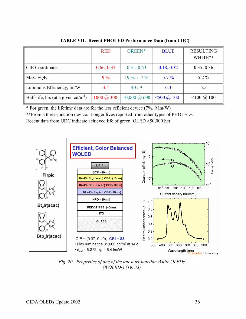
OIDA OLEDs Update 2002 36
TABLE VII. Recent PHOLED Performance Data (from UDC)
RED GREEN* BLUE RESULTING WHITE**
CIE Coordinates 0.66, 0.35 0.31, 0.63 0.18, 0.32 0.35, 0.36
Max. EQE 9 % 19 % / 7 % 5.7 % 5.2 %
Luminous Efficiency, lm/W 3.5 40 / 9 6.3 5.5
Half-life, hrs (at a given cd/m2) 1000 @ 300 10,000 @ 600 <500 @ 100 <100 @ 100
* For green, the lifetime data are for the less efficient device (7%, 9 lm/W) **From a three-junction device. Longer lives reported from other types of PHOLEDs. Recent data from UDC indicate achieved life of green OLED >50,000 hrs
Fig. 20 . Properties of one of the latest tri-junction White OLEDs (WOLEDs) (19, 33)
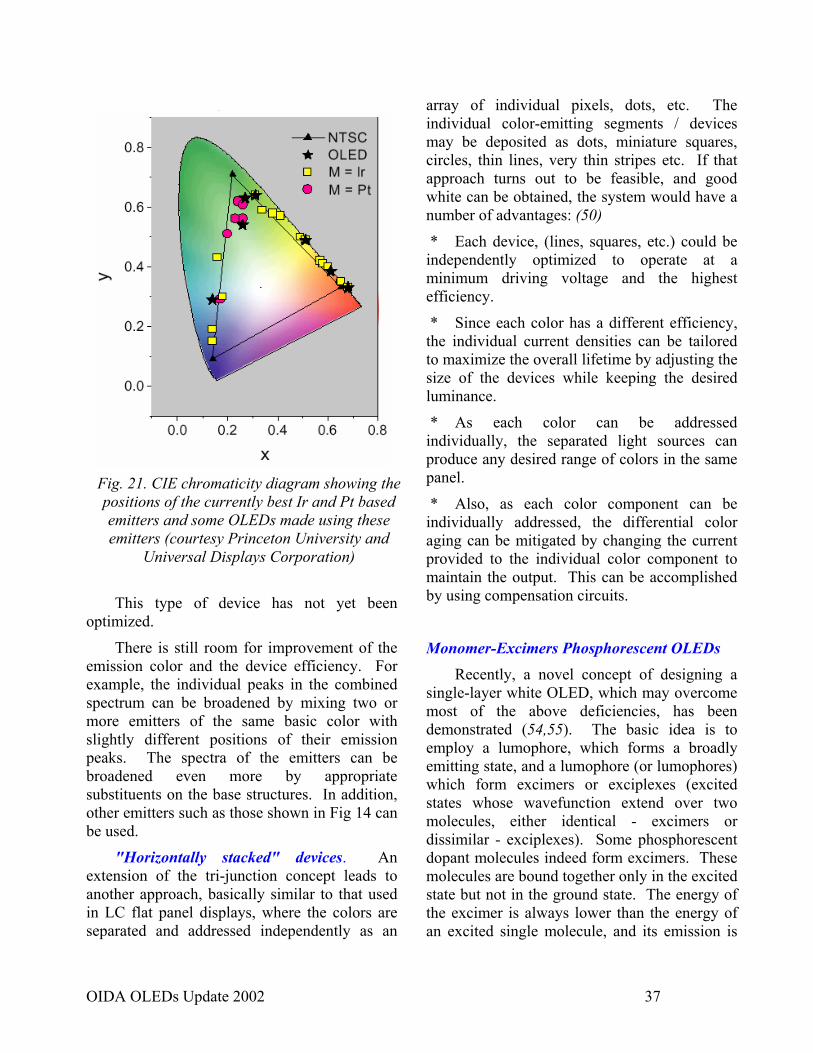
OIDA OLEDs Update 2002 37
This type of device has not yet been optimized.
There is still room for improvement of the emission color and the device efficiency. For example, the individual peaks in the combined spectrum can be broadened by mixing two or more emitters of the same basic color with slightly different positions of their emission peaks. The spectra of the emitters can be broadened even more by appropriate substituents on the base structures. In addition, other emitters such as those shown in Fig 14 can be used.
"Horizontally stacked" devices. An extension of the tri-junction concept leads to another approach, basically similar to that used in LC flat panel displays, where the colors are separated and addressed independently as an
array of individual pixels, dots, etc. The individual color-emitting segments / devices may be deposited as dots, miniature squares, circles, thin lines, very thin stripes etc. If that approach turns out to be feasible, and good white can be obtained, the system would have a number of advantages: (50)
* Each device, (lines, squares, etc.) could be independently optimized to operate at a minimum driving voltage and the highest efficiency.
* Since each color has a different efficiency, the individual current densities can be tailored to maximize the overall lifetime by adjusting the size of the devices while keeping the desired luminance.
* As each color can be addressed individually, the separated light sources can produce any desired range of colors in the same panel.
* Also, as each color component can be individually addressed, the differential color aging can be mitigated by changing the current provided to the individual color component to maintain the output. This can be accomplished by using compensation circuits.
Monomer-Excimers Phosphorescent OLEDs Recently, a novel concept of designing a
single-layer white OLED, which may overcome most of the above deficiencies, has been demonstrated (54,55). The basic idea is to employ a lumophore, which forms a broadly emitting state, and a lumophore (or lumophores) which form excimers or exciplexes (excited states whose wavefunction extend over two molecules, either identical - excimers or dissimilar - exciplexes). Some phosphorescent dopant molecules indeed form excimers. These molecules are bound together only in the excited state but not in the ground state. The energy of the excimer is always lower than the energy of an excited single molecule, and its emission is
Fig. 21. CIE chromaticity diagram showing the positions of the currently best Ir and Pt based emitters and some OLEDs made using these emitters (courtesy Princeton University and
Universal Displays Corporation)
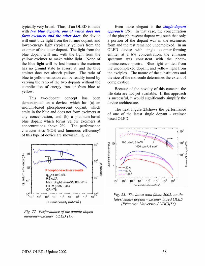
OIDA OLEDs Update 2002 38
typically very broad. Thus, if an OLED is made with two blue dopants, one of which does not form excimers and the other does, the device will emit blue light from the former dopant, and lower-energy light (typically yellow) from the excimer of the latter dopant. The light from the blue dopant will mix with the light from the yellow excimer to make white light. None of the blue light will be lost because the excimer has no ground state to absorb it, and the blue emitter does not absorb yellow. The ratio of blue to yellow emission can be readily tuned by varying the ratio of the two dopants without the complication of energy transfer from blue to yellow.
This two-dopant concept has been demonstrated on a device, which has (a) an iridium-based phosphorescent dopant, which emits in the blue and does not form excimers at any concentration, and (b) a platinum-based blue dopant which forms yellow excimers at concentrations above 2%. The performance characteristics (EQE and luminous efficiency) of this type of device are shown in Fig. 22.
Even more elegant is the single-dopant approach (19). In that case, the concentration of the phosphorescent dopant was such that only a portion of the dopant was in the excimeric form and the rest remained uncomplexed. In an OLED device with single excimer-forming emitter at a 6% concentration, the emission spectrum was consistent with the photo-luminescence spectra. Blue light emitted from the uncomplexed dopant, and yellow light from the exciplex. The nature of the substituents and the size of the molecule determines the extent of complexation.
Because of the novelty of this concept, the life data are not yet available. If this approach is successful, it would significantly simplify the device architecture.
The next Figure 23shows the performance of one of the latest single dopant - excimer based OLED:
Fig. 22. Performance of the double-doped monomer-excimer OLED (19)
Fig. 23. The latest data (June 2002) on the latest single dopant - excimer based OLED
(Princeton University / UDC)(56)
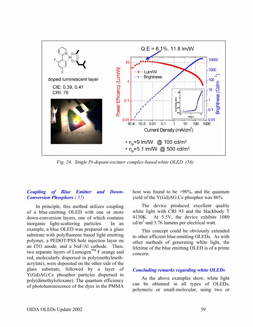
OIDA OLEDs Update 2002 39
Coupling of Blue Emitter and Down-Conversion Phosphors ( 57)
In principle, this method utilizes coupling of a blue-emitting OLED with one or more down-conversion layers, one of which contains inorganic light-scattering particles. In an example, a blue OLED was prepared on a glass substrate with polyfluorene based light emitting polymer, a PEDOT/PSS hole injection layer on an ITO anode, and a NaF/Al cathode. Then, two separate layers of LumogenTM F orange and red, molecularly dispersed in poly(methylmeth-acrylate), were deposited on the other side of the glass substrate, followed by a layer of Y(Gd)AG:Ce phosphor particles dispersed in poly(dimethylsiloxane). The quantum efficiency of photoluminescence of the dyes in the PMMA
host was found to be >98%, and the quantum yield of the Y(Gd)AG:Ce phosphor was 86%.
The device produced excellent quality white light with CRI 93 and the blackbody T 4130K. At 5.5V, the device exhibits 1080 cd/m2 and 3.76 lumens per electrical watt.
This concept could be obviously extended to other efficient blue-emitting OLEDs. As with other methods of generating white light, the lifetime of the blue emitting OLED is of a prime concern.
Concluding remarks regarding white OLEDs As the above examples show, white light
can be obtained in all types of OLEDs, polymeric or small-molecular, using two or
Fig. 24. Single Pt-dopant-excimer complex-based white OLED (56)
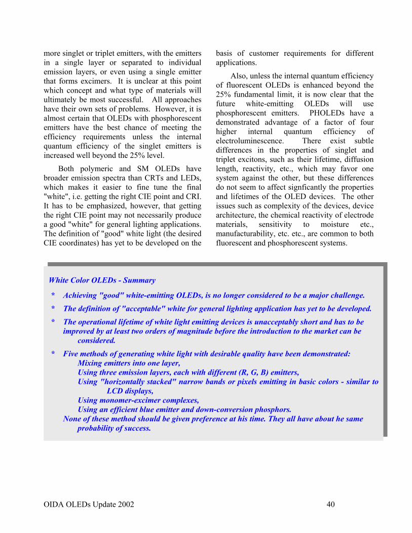
OIDA OLEDs Update 2002 40
more singlet or triplet emitters, with the emitters in a single layer or separated to individual emission layers, or even using a single emitter that forms excimers. It is unclear at this point which concept and what type of materials will ultimately be most successful. All approaches have their own sets of problems. However, it is almost certain that OLEDs with phosphorescent emitters have the best chance of meeting the efficiency requirements unless the internal quantum efficiency of the singlet emitters is increased well beyond the 25% level.
Both polymeric and SM OLEDs have broader emission spectra than CRTs and LEDs, which makes it easier to fine tune the final "white", i.e. getting the right CIE point and CRI. It has to be emphasized, however, that getting the right CIE point may not necessarily produce a good "white" for general lighting applications. The definition of "good" white light (the desired CIE coordinates) has yet to be developed on the
basis of customer requirements for different applications.
Also, unless the internal quantum efficiency of fluorescent OLEDs is enhanced beyond the 25% fundamental limit, it is now clear that the future white-emitting OLEDs will use phosphorescent emitters. PHOLEDs have a demonstrated advantage of a factor of four higher internal quantum efficiency of electroluminescence. There exist subtle differences in the properties of singlet and triplet excitons, such as their lifetime, diffusion length, reactivity, etc., which may favor one system against the other, but these differences do not seem to affect signficantly the properties and lifetimes of the OLED devices. The other issues such as complexity of the devices, device architecture, the chemical reactivity of electrode materials, sensitivity to moisture etc., manufacturability, etc. etc., are common to both fluorescent and phosphorescent systems.
White Color OLEDs - Summary
* Achieving "good" white-emitting OLEDs, is no longer considered to be a major challenge.
* The definition of "acceptable" white for general lighting application has yet to be developed.
* The operational lifetime of white light emitting devices is unacceptably short and has to be improved by at least two orders of magnitude before the introduction to the market can be considered.
* Five methods of generating white light with desirable quality have been demonstrated: Mixing emitters into one layer,
Using three emission layers, each with different (R, G, B) emitters, Using "horizontally stacked" narrow bands or pixels emitting in basic colors - similar to LCD displays, Using monomer-excimer complexes, Using an efficient blue emitter and down-conversion phosphors. None of these method should be given preference at his time. They all have about he same probability of success.
OIDA OLEDs Update 2002 41
5.1.5. Shelf Life Of importance is not only the operational
lifetime of the OLED device but also the shelf life under adverse conditions. It is now well known that the devices must be protected against the access of moisture and oxygen. At high temperatures, thermal expansion near the Tg may destroy devices at about that point, although excursions above Tg for a limited time may be survivable if the device is not operating.
The low work-function cathodes used in OLEDs are extremely reactive and must be protected. The metal-polymer interface is the weak link; degradation of this interface limits the device life even when it does not operate. Thus, packaging that would hermetically seal the devices will be required.
Rapid degradation of OLEDs is observed in the presence of even low concentrations of moisture. In most conventional OLED devices which are built on glass substrates this problem is addressed by encapsulating the devices using a glass lid sealed to the substrate by an adhesive - typically a UV curable epoxy resin. Desiccant is often added to the package to absorb residual moisture from the fabrication process and moisture diffusing through the epoxy seal. With plastic substrates, this method is not sufficient due to the high moisture permeability of the plastic itself.
Since the permeability of plastic substrates to oxygen and water vapor is orders of magnitude too high, novel barrier films or novel substrates will be required. Inorganic layers (or laminates of inorganic and organic layers) can provide sufficient barrier properties. Such inorganic layers must be pinhole free and robust. Brittle barrier layers would not withstand the flexing and stretching involved in a roll-to-roll process.
However, a new technique has already been developed to protect OLEDs on plastic substrates. It involves a deposition of a transparent flexible multi-layer organic-inorganic thin film barrier on top of the plastic using a hybrid process of cryo-condensation and polymerization of an organic monomer precursor followed by vapor deposition of nanoscale barrier layer. This multilayer hybrid barrier restricts permeation of both oxygen and moisture to non-measurable levels while retaining flexibility and transparency. Residual permeation is due to pinholes rather than bulk diffusion (58). At least 10,000 of useful life hrs of OLEDs are projected using this method of encapsulation.
To illustrate the need to examine every material component with respect to aging, results of an accelerated aging test are shown in Fig. 25. Two identical OLED devices were fabricated, except that the hole-transport molecules were different. The initial performance of the device with NPB (see the figure) severely decayed after the device had been exposed to elevated temperatures, while the device with the spiro-TAD molecule did not change (59). The effect is probably related to the difference in Tg:
Progress in designing stable systems has been largely empirical. Significant research is needed to obtain understanding of all the causes of OLED decay, including the effect of structural features. This has to include the development of analytical tools, particularly from selected disciplines in electrochemistry, photochemistry, and photophysics.
.
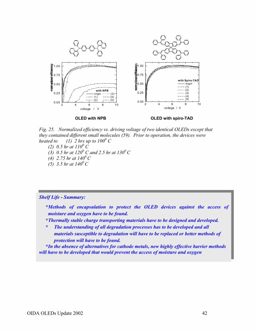
OIDA OLEDs Update 2002 42
2 4 6 8 100.00
0.25
0.50
0.75
1.00
with NPB virgin (3) (1) (4) (2) (5)
voltage / V
norm
aliz
ed e
ffici
ency
2 4 6 8 100.00
0.25
0.50
0.75
1.00
with Spiro-TAD virgin (1) (2) (3) (4) (5)
vo ltage / V
norm
aliz
ed e
ffici
ency
N N
OLED with NPB OLED with spiro-TAD Fig. 25. Normalized efficiency vs. driving voltage of two identical OLEDs except that they contained different small molecules (59). Prior to operation, the devices were heated to (1) 2 hrs up to 1000 C (2) 0.5 hr at 1100 C (3) 0.5 hr at 1200 C and 2.5 hr at 1300 C (4) 2.75 hr at 1400 C (5) 3.5 hr at 1400 C
Shelf Life - Summary:
* Methods of encapsulation to protect the OLED devices against the access of moisture and oxygen have to be found. * Thermally stable charge transporting materials have to be designed and developed. * The understanding of all degradation processes has to be developed and all
materials susceptible to degradation will have to be replaced or better methods of protection will have to be found.
* In the absence of alternatives for cathode metals, new highly effective barrier methods will have to be developed that would prevent the access of moisture and oxygen
OIDA OLEDs Update 2002 43
5.1.6. Current Distribution Over Large Areas
OLED devices operate at low voltages but with large currents. The impact of handling and distribution of large currents is not yet understood. Current distribution over large areas and connectors between the illumination panels and the circuitry are big challenges for OLED lighting. Also, the lighting industry will have to accept changes that must be made in the infrastructure in order to incorporate OLEDs.
The commonly used injecting electrode for OLEDs, indium-tin oxide (ITO) is not
conductive enough to deliver large currents to areas over several square inches. Alternatives are still not known. Significant effort is being expanded to replace ITO with conductive polymers etc., but the results are still inadequate. In displays, metal busbars are deposited along the edge of ITO lines to reduce power losses. However, for large single pixels or large general lighting panels this approach may not be practical. In the absence of ITO replacements, large light sources would have to be built up of smaller, matrixed "pixels", but this approach may not be economical.
5.1.7. Electrodes In order to get the light out of an OLED,
one of the electrodes has to be transparent. Indium-tin oxide (ITO) on a plastic substrate, which is now used as the transparent anode, has four basic problems:
Low conductivity (by about two orders of magnitude),
Needs to be cleaned and the work function has to be increased.
Is difficult to deposit, and brittle.
Granular surface may cause nonuniform- ities in the thickness of the active layers.
Commercially available substrates with the ITO layer have about 85% transmission. Inevitably, 15% of generated light is lost. It would be unreasonable to expect that 100% transparent conductors can ever be developed,
so about 10 - 15% loss of light due to absorption in the conductor has to be accepted as inevitable.
ITO-coated plastics, as received, have work function too low, about 4.7 eV but the value can be elevated by annealing (60) to over 150oC, but if the base material is plastic, there is a limit to which the temperature can be raised. Other methods include oxygen plasma treatment or acid treatment (61, 62). ITO must be cleaned before the use by chemical washing, scrubbing, ultra-sonification etc.
ITO is currently the only practical hole-injecting electrode material. In SM OLEDs is often coated with a more controlled conductive injection layer such as porphyrins, phthalocyanines, and charge transport media p-doped to become partially conductive. More recently, poly-3,4-ethylenedioxythiophene (PEDOT) has been used extensively. These materials effectively reduce the injection barrier between ITO and the hole-transport media. For polymeric devices, there is increased use of conducting polymers on ITO, such as
Current Distribution Over Large Areas - Summary:
The impact of handling large currents and low voltages is not understood. Major changes will have to be made in the lighting infrastructure to incorporate OLEDs
OIDA OLEDs Update 2002 44
polythiophene doped with polystyrene sulfonic acid, and also PEDOT. These polymers also make the surface much smoother than the original ITO surface.
Injection barriers for holes have also been reduced by insertion of an ultra-thin layer of metals such as Pt, Mn, Ni, Au, Pb, or Mg or other elements such as Ga, C, or Si between tha anode (ITO) and the hole transport layer (63).
Polyaniline has been also recently shown to be useful as a hole injection layer in OLEDs (64).
The current cost of the ITO-coated substrates is prohibitive, of the order of $200 per m2. Also, ITO is brittle and easily cracked and damaged. Large-scale web coating may reduce the cost of deposition, but ITO on plastic may not be a viable transparent anode material in high throughput roll-to-roll process, because the stresses would probably be too large. In addition to that, the conductivity of the ITO layers is lower than needed, by up to two orders of magnitude, particularly for large area distributed devices. The resistivity of the conductive layer should be less than about 50 Ω/sq, particularly for large areas.
Conducting polymer electrodes may offer a potential solution. Polymer OLEDs have been demonstrated using conducting polymers as anodes. There are several known candidates such as polyaniline, PEDOT, polypyrrole, etc. Sufficient transparency in the visible has been demonstrated. However, the conductivities of these materials in the form of optical quality thin films are still nearly two orders of magnitude too low for the lighting applications
(typically in the range of a few hundreds of S/cm). Some of this can be made up by using thicker films (surface resistance is then the only parameter). Unfortunately, thicker films tend to reduce transparency. This too can be improved. Oriented films are an opportunity. Orientation and the resulting improved structural order will lead to higher conductivity and to lower absorption (at least in the perpendicular polarization). Routes to oriented films of conducting polymer include self-assembly through the use of liquid crystalline materials (liquid crystalline conjugated polymers are known; liquid crystalline side chains can be used to induce order and orientation). The achievement of optical quality films of high conductivity metallic polymers is a major opportunity but also a difficult problem requiring a combination of synthesis and materials science.
Conductive poly(3,4-ethylenedioxythio-phene) (PEDOT) doped with poly(styrenesulfo-nate) was recently used as an anode in a functional OLED device without an indium tin oxide underlayer. (65).
Current cathode materials are limited to low-work function metals, such as Ca, Li, Mg or their alloys with Ag, although progress has been made recently by using LiF or CsF as dopants near the electrodes. These salts may enable the use of Al as an electrode. The combination of LiF and Al now appears to be the cathode material of choice. Even though both LiF and Al are less reactive to moisture than Na, Ca, Li etc., the LiF/Al combination may not alleviate the need to protect OLEDs against moisture.
Electrodes - Summary:
* There is a need for transparent anodes with conductivities greater than ITO * Cathode metals are chemically too reactive. Unconventional approaches are needed or alternatives have to be found. LiF/Al is currently the best cathode system.
OIDA OLEDs Update 2002 45
5.2. Manufacturing Issues
5.2.1. Synthesis of Materials. Pilot scale syntheses of active OLED
materials have not been carried out and large industrial scale syntheses of some compounds may never be needed. With 100 nm-thick films used for OLEDs and efficient deposition technology, approximately 10-7g of material would be used per m2 of an OLED panel. Therefore, 1 kg would coat up to 1010 m2 of OLED (about 10,000 square kilometers). Even allowing for a factor of 10 or so for deposition inefficiencies, this hardly represents a lucrative market for large chemical companies in spite of high value added and, therefore, no investment into the design of new more efficient OLED materials can be expected from large suppliers.
Research for novel OLED materials is and will be funded exclusively by either makers of OLED devices themselves - in cooperation with universities, or sub-contracted to makers of specialty chemicals. Sofar the burden of design, synthesis and qualification of the functional materials has been largely carried on the shoulders of few academic institutions (supported by small grants from a variety of sources), and to a small extend by industrial research groups with very limited budgets.
Purity of the functional materials has not been properly addressed. Most users assume that train or gradient sublimation increases purity to required levels. This may or may not be sufficient. Furthermore, small concentrations of impurities or molecular fragments may not be detectable by conventional techniques such as by mass spectroscopy, liquid chromatography analysis, etc. The elemental analysis may indeed show that the chemical is extremely pure, but undetectable traces of damaging impurities may escape detection. Conversely, impurities, which are damaging to inorganic semiconductors may be benign to organics. The experience with
organic photoreceptor materials suggests that the conventional analytical techniques are not sensitive enough to detect the critical impurities. Some impurities are benign but some may have to be reduced to below ppb (parts per billion) levels, mostly undetectable by the existing analytical techniques. New methodology to detect and analyze damaging impurities has to be developed. Functional specifications for many OLED components do not exist.
Manufacturing of all the chemicals used in small-molecule OLEDs is straightforward. All syntheses are done within 1-3 steps from commercially available materials, mostly with high yield and in short reaction times, without sub-zero temperature steps, and all can be carried out without vacuum techniques. Purification is relatively easy, mostly with column chromatography, which implies convenient pilot scale-up. Recrystallization and/or sublimation are also sometimes employed. For materials that are not very soluble or not very stable in solution, sublimation is more suitable.
Polymeric materials are inherently more difficult to synthesize and purify. Once an impurity is built into the polymer structure it cannot be removed except by a chemical treatment or a thermal conversion, where available. Any such treatment should be done without affecting the primary function of the polymer and the treatments are seldom 100% effective. In spite of these limitations, remarkable progress has been made in achieving the desired purity of polymers for OLEDs.
The "battle" between polymers and small molecules for the place in white OLEDs will continue for some time because neither system showed a clear advantage over the other. Phosphorescence emitters have not yet been used in combination with conjugated polymers and therefore little is known about the potential of increasing the internal quantum efficiency beyond what the polymeric OLEDs have achieved.
OIDA OLEDs Update 2002 46
5.2.2. Large-Area Coating and Depositions
On a lab scale, thermal evaporation and spin coating are used to build SM and polymeric OLED prototypes, respectively. These approaches are not useful for low cost, large area manufacturing. Roll-to-roll solution coating appears to be the only applicable low-cost technology. Vapor deposition technologies for web coatings exist, but will have to be adapted for the materials, desired layer thicknesses and uniformities needed for OLEDs. Conventional vacuum deposition can be used, but capital cost and materials wastage typically increase in quadrature with size. For high throughput, new ideas for roll-to-roll coating on flexible substrates are needed.
A key requirement for the fabrication of OLED displays is uniform film deposition over large areas as a consequence of the sensitivity of emission color and efficiency on film thickness. Conventional deposition using point sources is
unattractive. A novel extended linear evapo-ration source developed recently produces a film non-uniformity of less than 5% over a 300 - 400 mm substrate with a source to substrate separation of 120 mm. (66)
The demands on the thickness uniformity will be extremely high. Due to space charge limited conduction in most OLEDs, voltage variation scale with the third power of thickness, so uniformity is particularly important or current will sink through thin areas and lead to non-uniform aging or localized breakdowns. If charge traps are present in the materials due to the impurities, as has been demonstrated in many OLEDs, the thickness dependence becomes even higher.
No specifications for the device uniformity have yet been developed for lighting applications. Presently in the small-molecule technology it is thought that 5% thickness uniformity is adequate, but for large areas coatings it may not be sufficient.
Synthesis of Materials -Summary
* Extremely small amounts of active materials now used in OLEDs do not provide an incentive for suppliers to carry out research and development. Academic institutions have taken the early responsibility.
* Conventional analytical tools may not be sensitive enough to detect critical impurities. New analytical techniques and methods have to be developed
Large-Area Coating and Depositions - Summary
* Continuous web coating will be used to fabricate OLEDs for general lighting. It will present great challenges to maintain the desired uniformity of the device layers. The specifications still have to be developed.
* Methods of deposition of small molecules by continuous vapor deposition processes are being developed and tested.
OIDA OLEDs Update 2002 47
5.2.3 Plastic Substrates Even though glass substrates are used at the
present, OLEDs for general lighting will probably have to have plastic substrates, which will provide the needed flexibility and conformability, will have lower weight and thickness, and will enable roll-to-roll coating. Plastic is highly desirable for lightweight, rugged, conformable or flexible applications. However, no suitable plastic substrate is currently available. Biaxially oriented polyethylene terephthalate (PET) is widely used as the best available compromise but it cannot be heated over ~130 C. Quality control on rolls of PET is appallingly bad by thin film standards. Spikes >100 nm in size, long edges (non-uniform stretch), scratches, bubbles, needles of crystals of foreign material and other inclusions are plentiful. Lack of good quality substrate may seriously impede the development of plastic OLEDs. The substrates must have high chemical resistance to common coating solvents, scratch resistance, low oxygen permeability - below 10-5 cc.m2.day.atm and low water permeability (<1µg/ m2.day), or additional protective barrier films would have to be added
Higher Tg substrates under development include polyethersulphone and polynorbornene, the latter of which suffers from poor mechanical strength. All are expensive and available only in limited quantities.
Thin-glass / polymer systems with thicknesses ranging from 50 to 100 µm represent another possibility. They show excellent barrier properties, combined with a sufficient bending property needed to shape displays in various application (67). For OLED display applications, substrate materials must meet stringent requirements: Optical transmittance of 90% from 400 nm to 700 nm and 85% with ITO coating. The substrate must be stable under heat. The instabilities under heat would preclude all operations requiring higher deposition, conditioning, or drying temperatures. Thermal expansion should be <5 x 10⁻⁵ / oC with 5% variation. Thermal shrinkage, 0.1% after 200oC for 1 hr, with 5% variation. The specifications for general lighting purposes are expected to be similar.
The one OLED-related issue here besides the transparent conductor material itself is the surface roughness requirements. A common specification is surface R< 20 nm. Applied Films has recently developed a “smooth” ITO for OLEDs with claims of R< 10 nm.
Also, the polymeric substrate must be essentially free of low molecular materials. Ingredients that could leach out of the bulk and mix with the OLED active components could negatively affect the performance of OLEDs.
Plastic Substrates - Summary:
There is a need for a new OLED substrate polymer with
* High thermal resistance to at least 200oC - shrinkage or expansion free (see above) * Optical transmittance of 90% from 400 nm to 700 nm and 85% with ITO coating * Minimum surface roughness * Low oxygen permeability (<10-5 cc.m2 per day) * Low water permeability (<1 mg/m2 a day) * Virtual absence of defects (crystals, bubbles, filaments etc)
No commercial material meets all these requirements. Methods will have to be found to mitigate the defficiencies of present materials (Mylar TM etc.)
OIDA OLEDs Update 2002 48
5.3. Summary: Technology Roadblocks. Integration
From the above chapters one can list the individual challenges and technology roadblocks. The list is not complete because each challenge has a number of smaller challenges or is waiting for a solution of several problems. These are the major ones.
* The white OLED luminous efficiency must be increased more than 10 times.
* The operating life of white OLEDs is too short. It has to be increased more than 100 times.
* Light extraction from OLEDs is poor. A factor of 3 - 4 improvement is needed.
* The quality of white color is acceptable but still subject to improvements.
* The OLED devices are too complex (too many layers).
* There are no real alternatives to ITO. Existing alternatives are still unsatisfactory.
* There are no ideal alternatives to the cathode metals. The LiF/Al is the currently preferred combination.
* Barrier materials are still insufficient. Their effectiveness has to be improved.
* Substrate plastics tolerating high temperatures have not yet been identified.
* The impact of handling large currents is not understood.
* Manufacturing technology for large OLED devices has not been established.
From the above chapters it is clear that substantial progress is being made in each category of challenges to achieve the goal of making OLEDs a commercial source of light for general illumination. The analysis of the current technological obstacles also shows that none of them is insurmountable. So it is only a matter
of time and resources before the goal is achieved.
At this time, progress is being made on different fronts, in many competing (and also cooperating) laboratories, industrial, academic and governmental. The main reason why OLEDs have not yet reached the desired attributes (high power efficiency and long life, the best color, etc. at the same time) is that the latest findings and breakthroughs have not yet been integrated. For example, devices made to demonstrate high internal quantum efficiency have not been thoroughly protected against the access of moisture. Devices, in which the multilayer protective coatings were tested, were not designed for efficiency. The devices that showed near perfect color rendition and position on the chromaticity diagram were not constructed to achieve the optimum luminance and life, etc., etc.
Most devices have been built and tested with the only purpose to evaluate novel emitters, blocking layers, injection facilitators, charge transport media, electrodes materials, etc., and to verify fundamental photophysical parameters. These tests did not require the time-consuming protection against moisture. Not much progress has been made in increasing the extraction efficiency. The concepts are known, but their implementation represents additional steps in fabrication, which are often unnecessary at this time. The devices have not been optimized because the decision which materials and white-light generating concepts will be used has not yet been made.
The integration will eventually happen and will be supported by functional performance models. The model will eventually include all parameters that affect the device performance: Driving voltage; temperature, charge carrier mobilities of the hole and electron transporters; the HOMO and LUMO levels of all components; the work functions of electrodes; the thicknesses of each layer, the density of emitters, the exciton lifetimes etc. etc. Once the
OIDA OLEDs Update 2002 49
integration begins, we will see substantial improvements in power efficiency and life. It is quite natural that the integration of the "best-of-OLEDs" will happen in the industrial labs which will be ready to manufacture the devices.
Based on today's knowledge, OLEDs for general lighting will use phosphorescent emitters. However, the choice between polymers and "small molecules", the selection of the type of materials and the device architecture (the number and thicknesses of layers etc) cannot be made at his time. Both systems have an equal chance.
OLEDs are already commercialized in display applications. The field experience with the performance and stability of the devices will
accelerate the development of OLEDs for general lighting.
The half-life near 50,000 hrs has already been achieved, with well-encapsulated devices, even though only with green PHOLEDs and at lower than needed luminance. The external quantum efficiency of nearly 20%, which, under the particular conditions corresponded to 40 lm/W, has been demonstrated for green PHOLEDs, before any attempt was made to improve outcoupling. The outcoupling efficiency by a factor 2.5 has already been demonstrated. It is therefore safe to assume that the goals described above will be met as soon as all the breakthroughs and findings are integrated.
5.4 OLED Workshops Conclusions and Recommendation
OLEDs for SSL Workshop November 30 - December 1, 2000, Berkeley, CA OLEDs for SSL Update Workshop April 5, 2002, Berkeley, CA
Both workshops on OLED-based SSL for general illumination were attended by approximately 40 representatives from industry, universities, government laboratories, the US Department of Energy, and consultants. The main objective of the workshops was to identify and qualify roadblocks in the way of making OLEDs a technology aimed at replacing the fluorescent lighting, and to develop consensus on the course of action to achieve this ambitious goal.
A general agreement was reached that there are no fundamental obstacles for OLEDs to become a technology of choice for general lighting. However, there still exist a number of "incremental" roadblocks that have to be overcome, many of which may require inventions or major breakthroughs.
It was also agreed that most of these roadblocks are materials related. The rate of progress will depend on the success in designing and synthesis of novel high performance, stable materials components of OLED devices to replace those that are still deficient.
Part one (5.4.1) presents the current status of the OLED performance and development,
Part two (5.4.2) of the conclusions deals with the strategy for achieving stable energy-efficient OLED devices capable of competing with and eventually replacing fluorescent lights.
Part two (5.4.3) describes the long term research, development and manufacturing issues and presents recommendations.
OIDA OLEDs Update 2002 50
5.4.1 Current Status of OLEDs Power Efficiency of OLEDs
No fundamental insurmountable roadblocks in increasing the device efficiency to the desired levels have been identified. In fact, given recent improvements, it is recommended that the application for general lighting be pursued aggressively as soon as possible.
In summary, the current best luminous efficiency of phosphorescent white OLEDs is off the desired target by a factor of about 15. This estimate is based on the performance of the latest devices with phosphorescence emitters. This represents a substantial improvement over the situation about a year ago. The maximum internal quantum efficiency of green PHOLEDs at luminances near 100 cd/m2 is now near 100% and other colors are slowly approaching the same value. OLEDs with fluorescence emitters have much lower efficiencies, primarily due to the spin-statistics rule that only 25% of the charge recombinations lead to singlet excited states, and the low photoluminescence efficiency of the emitters. The photolumines-cence efficiency Φf can approach unity but only in dilute solutions. General problem is to maintain high Φf in solid state. Few materials have Φf greater than 50% in OLEDs. The peak power efficiency achieved to date for green is 76 lm/W.
However, the external efficiency ηext is still less than 20%. Over 80% of the light is lost to internal absorption and waveguiding in a simple planar device. The internal reflection of photons caused by high refractive indices of the layer materials is the main cause of poor extraction efficiency.
The external efficiency ηext is related to the internal efficiency by a formula
ηext = Re ηint
where Re is the coefficient of extraction. Obviously, there is a need to increase Re to the maximum possible value.
Even here, the optimism that the extraction efficiency can be improved is justified. For example, the extraction efficiency Re (the number of photons emitted to the exterior of OLEDs per number of photons generated inside the device) for isotropic (small molecular) systems has already been raised from about 18% to 35%, and in the case of polymeric emitters, to 45%. This was achieved by proper engineering the conductor (electrode) surface pattern. In these experiments it was shown that by changing the reflective pattern the photons could be redirected to reach the “escape cone” and leave the device. It is estimated that the extraction efficiency can be increased by as much as a factor of four to near 80% with appropriate patterning of the reflective cathode and the device surface.
Other ways of improving the luminous efficiency (lm/W) exist and are being explored. These include various voltage reduction strategies outlined in the text of the Roadmap. It is imperative that device modeling is initiated to optimize the device performance for maximum efficiency.
There was much discussion regarding the luminance level required. If the entire ceiling is emitting, a luminance level of 100 cd/m2 is necessary (this will give 100 cd/m2 at desk level if room is large). For a portion of the ceiling (such as in a common office), the needed luminance is near 1000 cd/m2. The lighting industry will not accept greater than about 850 cd/m2 for glare reasons and, for 850 cd/m2, approximately 12% of the ceiling area would be required for lighting. The value of optimal luminance will, of course, depend on the building / room architecture and intended use of the light source.
A luminance level of 850 cd/m2 was decided to be the first level target for efficiency and stability projections.
The short-term efficiency target is >100 lm/W. To achieve this target, a needed efficiency improvement of 2x, 3x and 4x for G,
OIDA OLEDs Update 2002 51
R, and B, respectively, is estimated. A 60 – 100 lm/W white light source was considered achievable by 2005 - 6.
Operational Life All device life testing is done in accelerated
tests at elevated temperatures and the data are extrapolated to realistic conditions. In some labs the life tests are carried out at 70o C a scaling factor of 40 is used. For example, if the device lasts 60 days, it is assumed that it would live 20,000 hrs at 25 o C, etc. This method involves some risks. Any excursion to high temperatures may induce structural changes that would not occur under realistic conditions.
For fluorescent white light OLEDs, the useful lifetime of 3 - 4,000 hrs from 850 cd/m2 with 20% decay is estimated using the algorithms described in Chapter 5.1.2. As discussed above, these relatively low values do not represent the possibilities of OLEDs because the overall integration has not yet been attempted. Lower lifetimes, of the order of 500 hrs have been demonstrated with phospho-rescent white OLEDs. Again, the difference is meaningless since extensive lifetime studies have not yet been done. Phosphorescent OLEDs are relatively new technology.
Short device life is still a major obstacle to commercialization of OLEDs for general lighting. Life testing is not a priority in display applications, where the current lifetimes are already close to the desired values. Consequently, there is no systematic highly focussed research going on that would address life as a main issue. It was felt that here lies a prime opportunity for the government / industry / academia collaboration.
Color It was concluded that using two dopants to
create the appropriate color is an easier proposition than trying to adjust the
concentration of three dopants. The two-dopant approach is viewed as a feasible one because most OLED emitters have very broad emission spectra. Finding the optimum spectra to mix to give the appropriate CIE and color rendition is important. No problems were envisioned with obtaining the appropriate spectra because of the infinite variations available for organic small molecules.
It is generally agreed that achieving the white with CRI > 70, CIE coordinates (0.32, 0.32) and the spectral output most resembling sunlight is not a major problem.
It was emphasized that a significant materials research is still needed to identify emitters with sufficient stability and the right emission spectra. In general, however, it was felt that achieving the white color with high rendition is achievable with no major roadblock, provided that significant research is carried out to support this activity.
Differential aging of different color emitters was originally viewed as a major problem. Uneven rates of degradation would result in color shifts and deterioration of the quality of white. However, an increased inventory of emitters made it possible to identify compounds that age with comparable rates. So differential aging is no longer viewed as a major problem. As more and more emitters are developed, the stability of white will be assured.
Cost Establishing a manufacturing platform or
process flow would impact the OLED development work and, obviously, the time to market. It is a misconception that technology development and manufacturing process development are separate issues that should be addressed sequentially or by different groups. A two-track approach to working on manu-facturing issues was proposed.
OIDA OLEDs Update 2002 52
* Develop OLED technology that meets the performance specification at acceptable cost. The cost target for near term goals is $20/m2. It is estimated that the present cost for OLED technology is $400/m2.
* Perform basic materials development work to simplify and reduce the manufacturing costs.
Addressing cost, the group emphasized that a factor of 10-20 decrease in cost from the best present day achievable is required to realistically sell OLEDs into the SSL market. It is believed that the manufacturing cost could be $50/m2 in 1003 and $20/m2 in 2006, under the assumption that the critical issues are addressed now.
The key issues to address are:
* organic deposition technology, and
* encapsulation when the devices are built on web and scaled up to 36” wide web running at 200’/min
Nonexistent Infrastructure The problem of driving the light fixtures
with high currents at low voltages has been raised at several occasions. However, this issue, although generally recognized as very important, was not discussed in any detail because few of the Workshop participants felt competent to address it.
Drive conditions were discussed. Clearly, constant current drive is better for operational stability and for dimming capability, however, no one could address the electronic complexities / cost regarding this issue.
The concept of a feedback loop to the lamp power controller was also discussed. This should not add significantly to the cost of the fixture and would extend the lifetime and maintain a constant luminance level over the fixture lifetime. With constant luminance, the electrical power will be lowest at the start of life and highest at the end.
Eventually, designers will incorporate the capabilities of new lighting capabilities into new fixture designs. However, OLED solid state lighting should be compatible with the existing fluorescent light formats so that these can be easily replaced by OLED fixtures. In other words, existing buildings must be easily retrofitted with OLED lighting.
A segmented lamp, with individually patterned emitters, may be a good format for adjusting the color balance (mood) of the lamp. Also may be able to provide a feedback loop to the power controller to maintain the color balance during lifetime.
5.4.2 Strategy for making OLEDs the Technology of Choice for General Lighting.
Achieving white light with the desired position on the CIE chromaticity diagram and with high color rendition index, CRI, is within the reach of both polymeric and SM OLEDs. Many emitters with the desirable emission spectra are already available and many more will be designed. The power efficiency requirement of at least 100 lm/W is also viewed as achievable, provided that a significant research and development program to design new stable materials is undertaken and the light extraction efficiency is improved.
OLEDs will be useable for general lighting after the following improvements and changes are made:
* The white light device efficiency is increased by at least a factor of 15. * The operational lifetime of white OLEDs is increased by approximately 100 times.
* Flexible plastic substrates, free of defects, which will allow high temperature deposition of the device components, are identified.
OIDA OLEDs Update 2002 53
.* Manufacturability of large area (distributed) light sources is established
* The issues of packaging and protection against ambients are resolved.
* The infrastructure for handling large electric currents (at low voltages) to drive OLEDs is in place.
It is agreed that these are the main areas of future development activities and each will require substantial investments in manpower, time and money.
It has to be noted that substantial progress has been already made in each of these individual areas but the improvements have not yet been integrated into one device.
There are two main groups of OLED devices, both operating on the same principle but using two different groups of materials: "Small molecule" (SM) OLEDs, and polymeric OLEDs (POLEDs). Both materials systems have achieved about the same level of stability, device efficiency, color design etc., and therefore, it is not advisable to prefer one of these two sets of materials to the other at this time.
SM OLEDs: This group appears to have achieved more attention because the synthesis and mainly purification of organic small molecules is easier and straightforward. However, the devices based on SMs are more complex than polymeric devices. They may have up to 10 layers not counting the substrate and the protective layers, which posses a significant manufacturing (and cost) challenge. In addition, the layers may be deposited by different techniques. The discovery that triplet states can be harvested in SM devices to produce photons and the use of monomer-excimer emitters gave this group a significant momentum.
POLEDs: The light emitting devices based on polymeric materials are typically simpler, with fewer layers. The polymers are deposited
by solution coatings, which is easier to scale up. In addition, the yield of singlet states was found to exceed 25%, which increased the chance of success of POLEDs. The use of phosphorescent emitters can also be considered. However, the synthesis and purification of the type of polymers used in light emitting devices is difficult. There appears to be only a minimum synthetic effort in place in the US. In spite of the lack of polymer synthetic activities in the USA it is reasonable to expect that POLEDs will continue to play an important role. European laboratories such as Cambridge Display Technologies have achieved a significant progress in the development of POLEDs and will be effectively competing with the SM devices in the US and Japan in display applications.
Conceivably, both materials groups can be combined in one type of devices. White color is achieved in both types of devices by mixing emitters or stacking layers with different emitters. White light of the desired T~6000K was generated in both groups of devices. Both have already achieved high CRI. New stable emitters have to be designed, synthesized and explored to achieve the desired operational life in both groups of devices.
5.4.3 Long-Term Research and Development Issues:
The research should focus on the following areas:
* Emitters, both triplet and singlet, and related photophysics,
* High mobility stable charge transport compounds with low injection barriers,
* Stable, highly conducting electrodes,
* Degradation mechanisms, device lifetime,
* Light extraction (outcoupling),
* Methods to get white light – optimum combination of emitters,
OIDA OLEDs Update 2002 54
* Device modeling to maximize performance,
* Large area designs,
* Protection against ambients,
* Low cost manufacturing,
* Packaging
Infrastructure and powering of OLED devices
A recommendation is made who should take the leadership role in each research category.
Emitters and Related Photophysics
Objective: to achieve 100% internal quantum efficiency of devices with all color emitters. To control the design of emitters to achieve any desired color in the chromaticity diagram
The recent development of high-efficiency phosphorescent emitters is an important breakthrough. The phosphorescent dopants increased the internal device efficiency to nearly 100% in the green. For other colors, however, the IQE still remains below 100%, for reasons that are not well understood. Recent development also pointed to the importance of excimers and exciplexes of phosphorescent emitters, particularly in an effort to design highly efficient white-emitting OLEDs. The use of singlet emitters, on the other hand, leads to less efficient devices, mainly because the population of singlet states appears to be limited to about 25% of all excitations, even though higher levels have been rumored. Also, luminescence yield of fluorescent emitters in solid state is typically far less than 100%. The issue of distribution of excitons between singlets and triplets has to be resolved. In multi-color devices leading to white-emitting OLEDs, the energy transfer between emitters has to be controlled or, if possible, eliminated.
This shows that basic understanding of related photophysical phenomena has to be enhanced, new efficient and stable emitters,
both singlet and triplet, have to be designed and synthesized, and the optimum conditions for emission identified. The knowledge and control of exciton diffusion length will be also helpful in developing the optimum device architecture. The research on understanding of related photophysical phenomena of emitters should be carried out in universities with an established expertise in photochemistry and photophysics. The development of new and stable emitters should be lead by industrial laboratories.
Charge Transport Materials (CT). Objective: To increase the rate of supply of charge carriers at lower voltages to the recombination zone by increasing the carrier mobility. To identify stable CT materials
Organic small molecules and polymers have typically low charge carrier mobilities. Hole mobilities in solid glasses of small molecules are only near 10-3 cm2/V.s. and in polymers, 10-5 to 10--8 cm2/V.s. Electron mobilities are even lower, on average by about two to three orders of magnitude. Even though the injection barriers for both holes and electrons are high, the injection-limited currents are proportional to the carrier mobilities. If the mobilities are increased, the voltage needed to overcome the injection barrier and keep the same current could be reduced. Low mobilities, especially for electrons thus cause the need for higher voltages to supply the carriers to the recombination zone and thus reduce the device efficiency.
Uneven rates of injection result in charge accumulation at interfaces between the charge transport layers, and consequently, to very high electric fields across some layers. This leads not only to the beneficial increase in charge injection of the slower-moving carrier but eventually to localized breakdowns due to uneven thicknesses and thus lead to degradation of the device. Therefore, it is desirable to identify materials, particularly electron
OIDA OLEDs Update 2002 55
transporting, with higher charge carrier mobilities. Also, the inventory of useful charge transporters has to be broadened to provide a better selection of HOMO and LUMO levels for minimizing the injection barriers. Industrial laboratories have been leaders in this area.
Stable, Highly Conductive Anodes and Cathodes
Objective: To identify highly conducting stable organic polymers as replacements for existing electrodes or at least to facilitate charge injection from electrodes.
Currently used anode, ITO, is expensive, brittle, too resistive to deliver current to large areas, and difficult to deposit. A novel conductive anode material is needed with high optical transmissivity, the desired work functions, high conductivity, stability and ease of deposition in uniform layers. "Synthetic metals" (conductive polymers) would be the best solution but the existing conductive polymers do not posses the desired conductivity, stability and transparency. Also, "synthetic metals" appear to be useful as injection- facilitating interfaces.
Similarly, the cathode metals (alloys of Ag with Li, Mg etc.) are too reactive, not only with the ambients but also with the adjacent device components, and have to be replaced, if at all possible. New metal systems including multilayer metals with a thin barrier layer, that are less reactive or conductive polymer systems with increased conductivity and high reflectivity need to be developed. The LiF/Al combination, which has been used in recent OLEDs, appears to be a good step forward.
The thin cathode and anode contacts even after material improvement target in this effort, are too resistive to distribute the high currents that will be inherent in large OLED panels. Interconnect structures must be designed that minimize the voltage losses associated with these high current levels. A second level, low
resistance power distribution structure needs to be developed that does not degrade performance and that is compatible with large panel manufacturing processes. Solving this problem will be a result of the collaborative effort of universities and the industry, driven by the latter.
Mechanism of Degradation
Objective: To develop understanding of pathways leading to photochemical and electrochemical changes in active materials and to develop means of preventing these reactions from occurring. To increase the lifetime of OLEDs
OLED devices can be bright at the onset of operation but the luminance decreases with time. The decay is faster at high luminances. There have been relatively few detailed studies of degradation mechanisms in both polymers and small molecules, and at interfaces between layers. Studies of the degradation mechanisms are important in determining the location of the problem and may lead to solutions. This may necessitate the development of more sensitive analytical methods.
Until the understanding of the principal degradation mechanisms is obtained, the OLED community will be working on a trial-and-error basis. Research in this area is urgently needed and should be encouraged. Major systematic studies of aging of all material components (substrates, electrodes, injection-modifying layers, charge transport molecules, emitters, dopants, exciton-blockers, etc.) are needed. This type of research would be best carried out in universities or national laboratories with an established expertise in electrochemistry and photochemistry.
Light Extraction, Outcoupling
Objective: to increase the OLED external quantum efficiency to about 60% - to increase the luminous efficiency of OLEDs.
OIDA OLEDs Update 2002 56
Industrial labs should assume the leading role of this research area, mainly because the area is closely related to manufacturing issues. Several techniques are being explored, each presenting a manufacturing challenge (applica-tion of index matching fluids, corrugated surfaces and interfaces, microcavities, micro-lenses, etc.). The current flat devices allow less than 20% of the generated light to escape. The rest is lost by internal absorption, waveguiding, etc. Innovative optical engineering approaches must be designed and implemented. Solving the light extraction problem is one of the major challenges facing the OLED community but the payoff would be high. Now, with the internal quantum efficiency of phosphorescent OLEDs near 100% and the external quantum efficiency approaching 20% (at least for some colors), a factor of 3 in enhancing the light extraction would be sufficient to make OLEDs competitive with other lighting technologies in terms of power conversion efficiency. The methods must be manufacturable at reasonably low cost. Industry lead with university and national laboratory support.
White Light
Objectives: Obtain white color OLEDs with the CIE coordinates (0.32, 0.32) and color rendition index >80
In a laboratory scale, an equivalent of (T=6,300K) with the CIE coordinates (0.32, 0.32) is within the reach of OLEDs, both small molecular and polymeric. However, the optimum methods of mixing colors have yet to be identified, and the decision how many colors have to be mixed to achieve the above coordinates with the desired CRI, has to be made. So far, white color with acceptable coordinates was achieved from as little as one single emitter up to three different emitters, not counting possible emission from the electron or hole transporters. New ideas have to be explored, such as a combination of three arrays of pixels of different color similar to LC
displays, with or without a diffuser, a blue or UV OLED with phosphors as a down convert or a multiplayer, stacked emitter with two or more color emissions. A key issue on all of these “white” light systems is color stability over time and operating conditions. Another OLED device structure issue is the method of interconnect individual OLED pixels or cells. The issue of white light quality will be best tackled by the collaborative effort of national laboratories (such as Lawrence Berkeley), academia and industry, while the structure of the white light device and interconnect schemes would be best addressed by industry with national laboratory support.
Device Modeling
Objective: To develop design principles for multi-layer, multi-component OLEDS with maximum performance.
Progress in the development of OLEDs has been largely empirical and so are the design principles. In view of the large number of parameters that determine the device performance, it is impossible to even estimate what the optimal device architecture ought to be (such as the number and thicknesses of the layers, dopant concentrations, etc). without a quantitative device model.
Following are some interdependent parameters that affect the device performance: work functions of the electrodes, the HOMO and LUMO levels of charge transport materials, (which together determine the height of the injection barrier), charge carrier mobilities, thicknesses of the layers, the applied voltage, the exciton diffusion lengths, the density of emitter sites, temperature, lifetimes of the excitons, triplet or singlet lifetimes, etc. The rational model has to include all these parameters. Models can be developed in any institution with mathematical skills, and the best approach appears to be a National laboratory lead with industry support.
OIDA OLEDs Update 2002 57
Large Area Design
Objective: to develop the methodology for designs of large area OLED device.
There are major challenges that need to be overcome to enable large area OLEDs. The reason for this is that a major practical failure mechanism for OLEDs are shorts caused by particles introduced in the manufacturing process. The chance of a short occurring increases exponentially as the device area increases. Hence novel large area designs need to be invented which either eliminate this failure mechanism or can tolerate it. Other challenges include power distribution – available device cathode and anode materials are too resistive to distribute the high currents that will be inherent in large OLED panels. Interconnect structures must be designed that minimize the voltage losses associated with these high current levels. A second level, low resistance power distribution structure needs to be developed that does not degrade performance and that is compatible with large panel manufacturing processes. Industry lead
Protection Against Ambients
Objective: To identify cost-effective methods of protecting OLED devices against the access of moisture, oxygen and CO2 to increase their shelf- and operational life.
The main degradation mechanisms in OLED devices are chemical reactions and electrochemical degradation of electrode materials, charge transporting molecules or polymers, dopants and excitons with ambients of moisture, oxygen and CO2. OLED devices must be protected from the access of moisture, oxygen and CO2. Since plastics films appear to be the leading candidate for the substrate enabling low-cost OLED manufacturing, selection of the film material and of the required coatings will be critical to performance and life.
Plastic film must stand up to the ambient conditions (heat, moisture, UV) and have minimal absorption of the emitted light. In addition, effective methods must be identified for complete protection of the sensitive OLED components against the access of moisture, oxygen and perhaps CO2. Research must be done to determine what level of moisture, oxygen and CO2 permeability is sufficient to meet the minimum life and performance targets.
A mixed organic/inorganic substrate should be investigated as an alternative approach to achieving the required permeability levels. Low cost methods of fabrication glass or glass/laminate substrates should be evaluated. Inorganic based panels will require the development or edge encapsulants to provide organic seals to meet permeability requirements
Plastic films must be identified or developed that meet the electrical, optical and mechanical requirement for OLEDD panels. Barrier coatings that are defect free over large areas, must be develop that can meet these permeability requirements. Deposition processes and equipment must be identified or developed that are compatible with large area panel or roll-to-roll manufacturing processes. The leading role belongs to industry with key support from the National laboratories.
Manufacturing Research.
Objective: to identify the optimum cost-effective methods for large scale manufacturing of OLEDs
Current OLED processes such as thermal evaporation, vacuum sputtering, spin coating and other deposition processes are not readily applicable to low cost web based manufacturing. Roll-to-roll coating is viewed as the most promising, low cost method of making OLED devices. Methods of incorporating evaporation / sublimation techniques need to be implemented in such a way that defects are not introduced into the structures. The experience
OIDA OLEDs Update 2002 58
acquired in the development and manufacturing of organic photoreceptors for electrostatic printers by roll-to-roll precision coatings could be applied in designing the manufacturing facilities for OLEDs. Alternative manufacturing methods such as large area panel processing need to be evaluated. These methods are more amendable to vacuum based processing and may provide a low cost, higher yield, more flexible manufacturing paradigm. The leading role belongs to the industry with national laboratory support from PNNL.
Packaging
Objective: To identify cost-effective packaging and interconnection methods OLED, to increase their shelf- and operational life.
The actual shape, configuration and interconnection of the lighting fixtures, including presentation to the customer must be developed. A thin, highly flexible OLED panel would require a more rigid structure to facilitate use in commercial or residential applications. Standards must be developed for the physical structure for OLED panels. This development will involve device makers, lighting companies, fixture designers, lighting engineers and building architects. The leading role belongs to the broader lighting industries with support from National laboratory and lighting research centers.
Infrastructure and Powering of OLED Devices.
Objective: To develop understanding of issues related to using light sources, which operate under d.c. conditions, low voltages and high currents
Even though this is not a purely scientific topic, forward thinking has to be initiated as soon as possible. The delivery of large currents at low voltages will necessitate major changes in the ways power is handled and distributed in
buildings and also how the OLED devices are connected to the power source. Industry wide device, voltage, current and power quality standards must be developed if OLED lighting is to readily incorporated in buildings by architects, engineers, designers and builders. As device performance is advanced in this effort, a broad based cross-section of the OLED lighting community must be impaneled to develop these standards. Electronic industry groups such as the National Electronic Manufacturers Association (NEMA) must be tasked with developing design standards, device specification and Energy Star targets for the power sources that will drive and control electronics that will be used to monitor and control OLED devices.
Based upon these standards, concepts must be developed for power and control devices and circuits with specifications for voltage levels, current levels, power quality, EMI, efficiency, and life cycle. In cooperation with the Lighting industry, the Underwriters Laboratory must establish electrical, fire and environmental safety standards for OLED devices, power sources and control circuitry. The leading role belongs to the industries which plan to manufacture the OLED lighting devices and should be handled in collaboration with the national laboratories such as LB Lighting Research Lab, Underwriters Laboratories and institutions such as RPI Lighting Institute.
5.4.4 Goals and Milestones. The following projections are based on the
realistic rate of progress in achieving the main performance goals. No differentiation has been made between "small molecule" OLEDs and polymeric OLEDs because both groups of materials are viewed as having the same chance of success, provided that phosphorescent emitters can be used also with polymers. Also, an assumption has been made that an effective
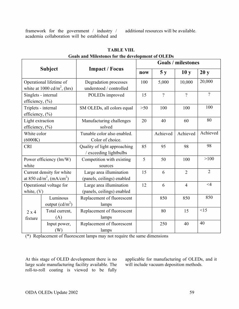
OIDA OLEDs Update 2002 59
framework for the government / industry / academia collaboration will be established and
additional resources will be available.
TABLE VIII. Goals and Milestones for the development of OLEDs
Goals / milestones Subject Impact / Focus now 5 y 10 y 20 y
Operational lifetime of white at 1000 cd/m2, (hrs)
Degradation processes understood / controlled
100 5,000 10,000 20,000
Singlets - internal efficiency, (%)
POLEDs improved 15 ? ? ?
Triplets - internal efficiency, (%)
SM OLEDs, all colors equal >50 100 100 100
Light extraction efficiency, (%)
Manufacturing challenges solved
20 40 60 80
White color (6000K)
Tunable color also enabled. Color of choice.
Achieved Achieved Achieved
CRI Quality of light approaching / exceeding lightbulbs
85 95 98 98
Power efficiency (lm/W) white
Competition with existing sources
5 50 100 >100
Current density for white at 850 cd/m2, (mA/cm2)
Large area illumination (panels, ceilings) enabled
15 6 2 2
Operational voltage for white, (V)
Large area illumination (panels, ceilings) enabled
12 6 4 <4
Luminous output (cd/m2)
Replacement of fluorescent lamps
850 850 850
Total current, (A)
Replacement of fluorescent lamps
80 15 <15 2 x 4 fixture
Input power, (W)
Replacement of fluorescent lamps
250 40 40
(*) Replacement of fluorescent lamps may not require the same dimensions
At this stage of OLED development there is no large scale manufacturing facility available. The roll-to-roll coating is viewed to be fully
applicable for manufacturing of OLEDs, and it will include vacuum deposition methods.
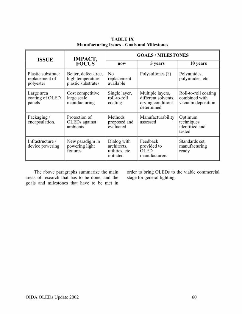
OIDA OLEDs Update 2002 60
TABLE IX Manufacturing Issues - Goals and Milestones
GOALS / MILESTONES ISSUE IMPACT,
FOCUS now 5 years 10 years
Plastic substrate: replacement of polyester
Better, defect-free, high temperature plastic substrates
No replacement available
Polysulfones (?) Polyamides, polyimides, etc.
Large area coating of OLED panels
Cost competitive large scale manufacturing
Single layer, roll-to-roll coating
Multiple layers, different solvents, drying conditions determined
Roll-to-roll coating combined with vacuum deposition
Packaging / encapsulation.
Protection of OLEDs against ambients
Methods proposed and evaluated
Manufacturability assessed
Optimum techniques identified and tested
Infrastructure / device powering
New paradigm in powering light fixtures
Dialog with architects, utilities, etc. initiated
Feedback provided to OLED manufacturers
Standards set, manufacturing ready
The above paragraphs summarize the main
areas of research that has to be done, and the goals and milestones that have to be met in
order to bring OLEDs to the viable commercial stage for general lighting.
OIDA OLEDs Update 2002 61
5.4.5 List of Attendees at the OIDA Solid State Lighting Workshops Nov. 30 - Dec. 1, 2000, Berkeley, CA
April 5, 2002, Berkeley, CA
(The following participants attended either the Nov. 30 - Dec. 1, 2000, or the April 5, 2002 Workshops or both.)
Kimberly Allen Stanford Resources Grat Oaks Blvd., Suite 200 San Jose, CA 95119 Ph: 408-360-8400 Fx: 408-360-8410 [email protected] Homer Antoniadis OSRAM OS 3870 North First Street San Jose, CA 95134 Ph: 408-456-4004 Fx:408-456-4305 [email protected] Norman Bardsley LLNL L-395, 7000 East Avenue Liovermore, CA 94551 Ph: 925-422-6008 Fx 925-422-8761 [email protected] Arpad Bergh OIDA 1133 Connecticut Avenue NW Washington, DC 20036-1023 Ph: 202-785-4426 Fx: 202-785-4428 [email protected] Jan Bernkopf Allen Technologies 900 E. Hamilton Ave, Suite 100 Campbell, CA 95008 Ph: 408-879-7326 Fx:408-879-7335
Dietrich Bertram Philips Research Weisshausstrasse 2 52066 Aachen Germany Ph; (+49) 241-6003-260 Fx: (+49) 241-6003-483 [email protected] James Brodrick DOE 1000Independence Ave, SW Washington, DC, 20585-0121 Ph: 202-586-1856 Fx: 202-586-4617 [email protected] Doug Brookman Public Solutions 5 Ingleside Avenue Baltimore, MD 21228 Ph: 410-719-8580 Fx410-719-0581 [email protected] Julie Brown Universal Display Corporation 375 Phillips Blvd Ewing, NJ 08618 Ph: 609-671-0980 Fx: 609-671-0995 [email protected]
OIDA OLEDs Update 2002 62
William Burgoyne Air Products & Chemicals 7201 Hamilton Blvd Allentown, PA 18195 Ph: 610-481-5718 Fx: 610-481-7719 [email protected] Paul Burrows Pacific NW Nat'l Lab 902 Batelle Blvd Richland, WA 99352 Ph: 509-375-5990 Fx: 509-375-3864 [email protected] Chips Chipalkatti OSRAM OS 100 Endicott Street Danvers, MA 01923 Phone: 978-750-2307 Fax: 978-750-2423 E-mail: [email protected] Nick Colaneri UNIAX 6780 Cortona Rd Santa Barbara, CA 93117 [email protected] George Craford LumiLeds Lighting 370 W. Trimble Rd San Jose, CA 94022 Ph: 408-435-6561 Fx: 408-435-5902 [email protected] Karl Drexler OSRAM OS 3870 North First St San Jose, CA 95134 Ph: 408-456-4029 Fx: 408-456-4305 [email protected] Anil Duggal General Electric 1 Research Circle, Room K1-4C25 Niskayuna, NY 12309 Ph: 518-387-7424 Fx: 518-385-5714 [email protected]
Raymond Fillion General Electric 1 Research Circle, CR&D, KWC 266 Niskayuna NY 12309 Ph: 518-387-6199 Fx: 518-387-5449 [email protected] Arthur Fischer Sandia National Labs Dept. 1123, MS 0601 PO Box 5800 Albuquerque, NM 87185-0601 Ph: 505-844-6543 Fx: 505-844-3211 E-mail: [email protected] Stephen Forrest Princeton University B210, Dept. of EE Princeton, NJ 08544-5263 Ph: 609-258-4532 Fx: 609-258-0119 [email protected] Jurrian Gerretsen Corning SP-FR-02-8 Corning, NY 14831 Ph: 607-974-0177 Fx: 607-974-0441 [email protected] Neil Greenham University of Cambridge Cavendish Laboratory CB3 0HE Cambridge England Ph: (+44) (0) 1223-766-301 Fx: (+44) (0) 1223-353-397 [email protected] Roland Haitz 25 Adair Lane Portola Valey, CA 94028 [email protected]
OIDA OLEDs Update 2002 63
Martin Hak AXTI 2019 Saturn Street Monterey Park, CA 91754 Ph: 650-315-6522 Fx: 801-697-7542 [email protected] Tukaram K. Hatwar Eastman Kodak Buiding 82B, 5th Floor, KP Rochester, NY 14650-2110 Ph: 716-477-8521 Fx: 716-477-6498 [email protected] Ian Hill Sarnoff 201 Washington Rd Princeton, NJ 08540 Ph: 609-734-2548 Fx: 609-734-2062 [email protected] Stewart Hough CDT 12920 Road 37 Madera, CA 93638 ph: 559-645-1034 Fx: 559-645-1035 [email protected] David Iams OIDA 1133 Connecticut Ave, NW Washington, DC 20036 Ph: 202-785-4426 Fx: 202-785-4428 [email protected] Ghassan Jabbour Univ. of Arizona Optical Sciences Center Tucson, AZ 85721-0094 Ph: 520-626-3295 Fx: 520-626-6219 [email protected] Steve Johnson LBNL 1 Cyclotron Rd, MS 90-3111 Berkeley, CA 94720 Ph: 510-486-4274 Fx: 510-486-4089 [email protected]
John Kerr LBNL 1 Cyclotron Rd, MS 62-203 Berkeley, CA 94720 Ph: 510-486-6279 Fx: 510-486-4995 [email protected] Thomas Kuech Univ. of Wisconsin 1415 Engineering Drive Madison, WI 53706 Ph: 608-263-2922 Fx: 608-265-4036 [email protected] Harriet Kung DOE-OBES 19901 Germantown Rd Germantown, MD 20874-1290 Ph: 301-903-1330 Fx: 301-903-9513 [email protected] David Lacey OSRAM OS 3870 North First Street San Jose, CA 95134 Ph: 408-456-4224 Fx:408-456-4305 [email protected] Qonnie Laughlin DOE FORS Bldg - Room 1J-018, MS 6A-116 Washington, DC Ph: 202-586-9632 Fx: 202-586-4617 [email protected] Eric Leonard Eastman Kodak Kodak Park, Bldg. 23 Rochester, NY 14652-4316 Ph: 585-477-1597 Fx: 585-477-2870 [email protected] Ron Lewis DOE 1000 Independence Ave, SW, Rm 1J018 Washington, DC 20585 Ph: 202-586-8423 Fx: 202-58 6-4617 [email protected]
OIDA OLEDs Update 2002 64
Heng Liu AXTI 2019 Saturn St Monterey Park, CA 91754 Ph: 323-278-0820 Fx: 323-278-0096 [email protected] Janice Mahon UDC 375 Phillips Blvd Ewing, NJ 08618 Ph: 609-671-0980 x206 Fx: 609-671-0995 [email protected] John McMahon Vitex Systems 1225 Tiros Way Sunnyvale, CA 94085 Ph: 510-848-8480 Fx: 253-423-9159 David Mentley Stanford Resources 2 Great Oaks Blvd., Suite 200 San Jose, CA 95119 Ph: 510-669-0521 Fx: 408-360-8410 [email protected] Alan Morrow Corning SP-FR-02-8 Corning, NY 14831 Ph: 607-974-3092 Fx: 607-974-3726 [email protected] Yoshi Ohno NIST 100 Bureau Dr. Gaithersburg, MD 20999-8442 Ph: 301-975-2321 Fx: 301-840-8551 [email protected] Raghu Padiyath 3M 3M Center, Bldg 201-15-23 St. Paul, MN 35144 Ph: 651-733-8952 Fx: 651-736-4430 [email protected]
Joe Paladino DOE - NETL 36 Collins Ferry Road Morgantown, WV 26507-0880 Ph: 304-285-4526 Fx: 304-285-4100 Mookkan Periyasamy DuPont I Technologies Experimental Station, Bldg 334/124 Willmington, DE 19880 Ph: 302-695-3433 Fx: 302-695-2341 [email protected] Edward Petrow Lincoln Technical Svcs. 60MacLeod Pond Rd Glenmoore, PA 19343 Ph: 610-321-2685 [email protected] Edward Pollock, Jr. DOE FORS Bldg - Room 1J-018, MS 6A-116 Washington, DC Ph: 202-586-9127 Fx: 202-586-4617 [email protected] Kathleen Richardson Schott Glass tech. 400 York Ave Duryes, PA 18642 Ph: 570-457-7485 x326 Fx: 570-457-3438 [email protected] Victor Roberts Lighting Research Center Rensselaer 21 Union St Troy, NY 12180-3352 Ph: 518-687-7188 Fx: 518-687-7120 [email protected] Charles Shank Director, LBNL 1 Cyclotron Rd, Mailstop 50A-4119 Berkeley, CA 94720 Ph: 510-486-5111 Fx: 510-486-6720 [email protected]
OIDA OLEDs Update 2002 65
Richard Silver Los Alamos Nat'l Lab MS D429 Los Alamos, NM 87545 Ph: 505-982-9109 Fx: 505-665-4292 [email protected] Jerry Simmons Sandia Nat'l Labs Dept. 1123, MS 0601 Albuquerque, NM 87185-0601 Ph: 505-844-8402 Fx: 505-844-3211 [email protected] Darryl Smith Los Alamos Natl Lab Electronics Research Group - MS D429 PO Box 1663 Los Alamos, NM 87545 Ph: 505-667-2056 Fx: 505-665-4036 E-mail: [email protected] Derrick Steinle Boeing Kennedy Space Center Capa Canaveral, FL 32815 Ph: 321-799-7237 Fx: 321-799-6834 [email protected] Frank Sterank LumiLeds Lighting 370 W. Trimble Rd, MS 91ML San Jose, CA 95131 Ph: 408-435-6636 Fx: 408-435-6039 [email protected] Milan Stolka Consultant 14 Park Circle Dr Fairport, NY 14450 Ph: 585-223-5309 Fx: 413-826-0259 [email protected]
John Talbot DOE FORS Bldg - Room 1M-048, MS 6A-116 Washington, DC Ph: 202-586-9455 [email protected] Ye Tao National Research Council - Canada M-50 Montreal Rd Ottawa, Ontario Canada K1A 0R6 Ph: 613-998-2485 Fx: 613-990-0202 [email protected] Paul Tivin AIXTRON 410 Tiogue Ave Coventry, RI 02816 Ph:401-828-7316 Fx: 401-828-1672 [email protected] Mark Thompson USC, L.J. Stabler Laboratory Los Angeles, CA 09989-0744 Ph: 213740-6402 Fx: 213-740-8594 [email protected] Yuan-Sheng Tyan Eastman Kodak 1999 Lake Ave Rochester, NY 14650-2017 Ph: 585-477-7884 Fx: 585-477-4545 [email protected] Jeffrey Tsao Sandia National Labs Dept. 1123, MS 0601 PO Box 5800 Albuquerque, NM 87185-0601 Ph: 505-844-7092 Fx: 505-844-3211 [email protected]
OIDA OLEDs Update 2002 66
Robert Jan Visser Vitex Systems 3047 Orchard Parkway San jose, CA 95134 Ph: 408-519-4437 Fx: 408-519-4470 [email protected] Steve Van Slyke Eastman Kodak B82 Research Laboratories 1999 Lake Avenue Rochester, NY 14650-2110 Ph; 585-722-1222 Fx: 585-477-6498 [email protected] Fred Welsh OIDA 1133 Connecticut Avenue NW Washington, DC 20036-1023 Ph: 202-785-4426 Fx: 202-785-4428 [email protected]
OIDA OLEDs Update 2002 67
6. Acknowledgements
This OLED roadmapping effort would not be possible without the financial support and active participation of the US Department of Energy's Office of Building Technology, State and Community Programs. The author is indebted to their support and help.
I express my gratitude to Arpad Bergh for his guidance and invaluable comments in drafting this Roadmap. I would also like to thank Alan Heeger, Homer Antoniadis, Ed Petrow, Chips Chipalkatti, Julie Brown, Anil Dugal, Steve Johnson, Mark Thompson, Steve Van Slyke, Ching Tang, T.K. Hatwar, John Ryan, Paul Burrows, Campbel Scott, Steve Forrest, Zoran Popovic, Ghassan Jabour and many other experts on OLEDs for helping me to put this overview together and for sending me all the data, comments, suggestions and advice, and for answering all the questions I had in the process. Sincere thanks are due also to Ed Petrow, Jim Broderick, Ray Fillion for critiquing the earlier version of the draft and changes they suggested. Special thanks are directed to Diane Burnes and David Iams for reminding me to stay on schedule.
OIDA OLEDs Update 2002 68
Appendix A: References.
1. J. R. Brodrick, OIDA OLED Workshop, April 5, 2002; Source: U.S. Lighting Market Characterization, Volume I – Lighting Inventory and Energy Consumption Estimate, Draft for Review, Arthur D. Little, Arlington, VA., March 5, 2002.
2. M. Kendall and M. Scholand, "Energy Savings Potential of Solid State Lighting in General lighting Applications" A.D.Little, Inc., Prepared for U.S. Department of Energy.
3. G. Jabbour, University of Arizona, OIDA OLED Workshop, April 5, 2002
4. A. Duggal, (General Electric), OIDA OLED Workshop Nov. 30, 2000
5. C. W. Tang, S. A. Van Slyke, C. H. Chen, Appl. Phys. Lett. 65, 3610 (1989).
6. J. H. Burroughes et al., Nature 347, 539 (1990).
7. R. Fillion (General Electric), OIDA OLED Workshop April 5, 2002
8. Ref. in M. A. Baldo et al., Nature 395, 151 (1998).
9. Baldo, D.F. O'Brien, Y. You, A. Shoustikov, S. Sibley, M. E. Thompson, and S.R. Forrest, Nature 395, 151 (1998).
10. S. Lamansky, J. Am. Chem. Soc. 123, 4304 (2001).
11. C. Adachi, et al., Appl. Phys. Lett., 78, 1622 (2001).
12. S.A. Van Slyke, C. H. Chen, and C. W. Tang, Appl. Phys. Lett., 69, 2160 (1996)
13. D. Lacey, OIDA OLED Workshop, April 5, 2002, ref. To Covion
14. H. Murata, Z. H. Kafafi, M. Uchida, Appl. Phys. Lett. 80, 189 (2002).
15. H. Murata, et al., Chem. Phys. Lett. 339, 161 (2001).
16. S.A. Van Slyke, (Eastman Kodak), OLED Workshop Nov. 30, 2000.
17. T.K. Hatwar (Eastman Kodak), OLED Workshop April5, 2002.
18. J. Brown, Universal Display Corporation - private communication
19 S.R. Forrest, Princeton University, OIDA OLED Workshop April 5, 2002
20. Z. D. Popovic, et. al., Xerox Research Centre of Canada, 2002.
21. J. Visser, OIDA OLED Workshop, April 5, 2002.
22. Covion, Advanced Materials 12, 42 (2000).
23. P. E. Burrows et al., MRS Spring Meeting, San Francisco, 2002.
24. S. Johnson, Draft review Chapter submitted to OIDA, July 2000
25 N. Greenham, OIDA OLED Workshop, April 5, 2002., MRS Spring Meeting, San Francisco, 2002.
OIDA OLEDs Update 2002 69
26. H. Becker, et al., Phys. Rev. B 56, 1893 (1997).
27. H.Becker et al., Synth. Met. 85, 1289 (1997).
28. M. Stossel et al., J. Appl. Phys 87, 4467 (2000)
29. S. Forrest, M. Thompson, MRS Spring Meeting, San Francisco, 2002, OIDA OLED Workshop, April 5, 2002.
30. Baldo et al., Phys. Rev. B62, 10967 (2000)
31. Young et al., Appl. Phys Lett. 80, 874 (2002)
32. Szmytkowski et al., Appl. Phys. Lett., 80, 1465 (2002)
33. R. C. Kwong, M. R. Nugent, T. Ngo, K. Rajan, L. Michalski, M. S. Weaver, T. X. Zhou, Y-J. Tung, R. Hewitt, M. Hack, J. J. Brown, Ewing, NJ., Meeting of the Society for Information Display, Boston, May 20-24, 2002, presentation 52.3
34. I. Schnitzer and E. Yablonovich, Appl. Phys. Lett., 63, 2174 (1993).
35. G. Gu et al., Opt. Lett. 22, 396 (1997).
36. C. Madigan et al., Appl. Phys. Lett. 76, 1650 (2000).
37. T. Yamasaki et al., Appl Phys. Lett. 76, 1243 (2000).
38. B. Ruhstaller, S.A.Carter, S.Barth, H.Riel, W.Riess, and J.C.Scott, J.Appl. Phys. 89, 4575 (2001).
39. L. S. Hung, C. W. Tang, M. G. Mason, App. Phys. Lett. 70, 152 (1997)
40. G. Jabbour et al., Appl Phys. Lett. 71, 1762 (1997).
41. W. Reiss et al., Syn. Met. 99, 213 (1999).
42. M. Stossel et al., Syn. Met. 111, 19 (2000).
43. G. E. Jabbour et al., Appl. Phys. Lett. 80, 2026 (2002).
44 M.D.Alexander and D.S.Dudis, MRS Spring Meeting, San Francisco, 2002.
45. G.G. Maliaras and J. C. Scott, J. Appl. Phys. 83, 5399 (1998)
46. Y. Shen, M. W. Klein, D. B. Jacobs, J. C. Scott, G. G. Maliaras, Phys. Rev. Lett. (2001), J. C. Scott, MRS Spring Meeting, San Francisco, 2002
47. J. C. Scott, G. G. Malliaras, J. R. Salem, P. J. Brock, L. Bozano, and S. A. Carter, Proceedings, SPIE Mtg. 1998.
48. Y. Ohno, NIST, OLED Workshop Nov. 30, 2000
49. J. Brooks and M. Thompson, MRS Spring Meeting, San Francisco, 2002
50. M. Thompson, private communication.
51. J. Kido, Science, 267, 1332,(1995)
52. P. E. Burrows, S. R. Forrest, S. P. Sibley, and M.E. Thompson, Appl. Phys. Lett., 69, 2959 (1996)
OIDA OLEDs Update 2002 70
53. Z. Chen, P. E. Burrows, V. Bulovic, S.R. Forrest, and M. E. Thompson, Science 276, 2009 (1997).
54. B. W. Andrade, M. E. Thompson, and S. R. Forrest, Advanced Mat. , Feb. 2002
55. B.W. D'Andrade, S.R. Forrest, J. Brooks, V. Adamovich, and M.Thompson, MRS Spring Meeting, San Francisco, 2002.
56. S.R Forrest, M. Pfeiffer, B. D. Andrade, M. A. Baldo, S. Moller, J. J. Brown, R. Kwong, M. E. Thompson, J. Brooks and V. Adamovich, Meeting of the Society for Information Display, Boston, May 20-24, 2002
57. A.R. Duggal, J.J. Shiang, C. M. Heller, D.F. Foust, Appl. Phys. Lett. 80, 3470 (2002)
58. P. E. Burrows et al., MRS Spring Meeting, San Francisco, 2002.
59. H. Becker, (Covion), presentation at the FPD Manufacturing Technology Conference, Feb. 2-3, 2000, San Jose, CA.
60. C. W. Tang, S. V. Slyke, Eastman Kodak Co., private communication.
61. C. C. Wu et al., Appl. Phys. Lett. 70, 1348 (1997)
62. F. Li et al., Appl. Phys. Lett. 70, 2741 (1997).
63. C. Qiu, H. Chen, Z. Xie, M. Wong, H-S. Kwok, Hong Kong University of Science and Technology, Clear Water Bay, Hong Kong, Meeting of the Society for Information Display, Boston, May 20-24, 2002, presentation 47.2
64. B. Wessling, B. Werner, J. Posdorfer ,Ormecon Chemie GmbH & Co. KG, Ammersbek, Germany H. Becker, S. Heun, H. Vestweber, Covion Organic Semiconductors GmbH, Frankfurt, Germany. Meeting of the Society for Information Display, Boston, May 20-24, 2002, presentation P-99
65. W. H. Kim, Z. H. Kafafi, Naval Research Laboratory, Washington, DC. Meeting of the Society for Information Display, Boston, May 20-24, 2002, presentation 37.1
66. S. A. Van Slyke, A. Pignata, D. Freeman, N. Redden Eastman Kodak Co., Rochester, NY, D. Waters, H. Kikuchi, T. Negishi Ulvac Japan, Ltd., Chicasaki, Japan, H. Kanno, Sanyo Electronics Co., Ltd., Gifu, Japan, Meeting of the Society for Information Display, Boston, May 20-24, 2002, presentation 27.2
67. A. Weber, S. Deutschbein, A. Plichta,Schott Displayglas, Mainz, Germany A. Habeck Schott Glas, Mainz, Germany. Meeting of the Society for Information Display, Boston, May 20-24, 2002, presentation 6.3.
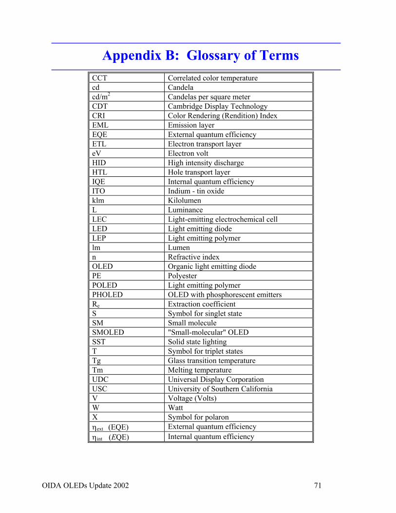
OIDA OLEDs Update 2002 71
Appendix B: Glossary of Terms
CCT Correlated color temperature cd Candela cd/m2 Candelas per square meter CDT Cambridge Display Technology CRI Color Rendering (Rendition) Index EML Emission layer EQE External quantum efficiency ETL Electron transport layer eV Electron volt HID High intensity discharge HTL Hole transport layer IQE Internal quantum efficiency ITO Indium - tin oxide klm Kilolumen L Luminance LEC Light-emitting electrochemical cell LED Light emitting diode LEP Light emitting polymer lm Lumen n Refractive index OLED Organic light emitting diode PE Polyester POLED Light emitting polymer PHOLED OLED with phosphorescent emitters Re Extraction coefficient S Symbol for singlet state SM Small molecule SMOLED "Small-molecular" OLED SST Solid state lighting T Symbol for triplet states Tg Glass transition temperature Tm Melting temperature UDC Universal Display Corporation USC University of Southern California V Voltage (Volts) W Watt X Symbol for polaron ηext (EQE) External quantum efficiency ηint (EQE) Internal quantum efficiency
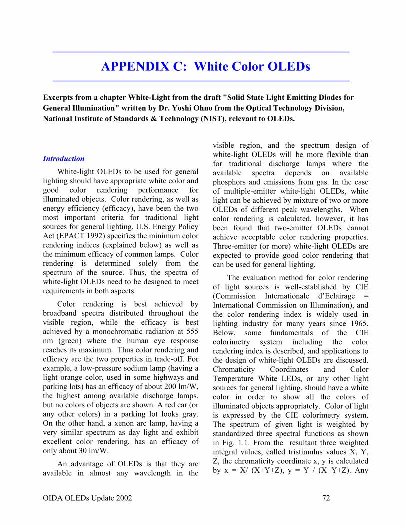
OIDA OLEDs Update 2002 72
APPENDIX C: White Color OLEDs
Excerpts from a chapter White-Light from the draft "Solid State Light Emitting Diodes for General Illumination" written by Dr. Yoshi Ohno from the Optical Technology Division, National Institute of Standards & Technology (NIST), relevant to OLEDs.
Introduction White-light OLEDs to be used for general
lighting should have appropriate white color and good color rendering performance for illuminated objects. Color rendering, as well as energy efficiency (efficacy), have been the two most important criteria for traditional light sources for general lighting. U.S. Energy Policy Act (EPACT 1992) specifies the minimum color rendering indices (explained below) as well as the minimum efficacy of common lamps. Color rendering is determined solely from the spectrum of the source. Thus, the spectra of white-light OLEDs need to be designed to meet requirements in both aspects.
Color rendering is best achieved by broadband spectra distributed throughout the visible region, while the efficacy is best achieved by a monochromatic radiation at 555 nm (green) where the human eye response reaches its maximum. Thus color rendering and efficacy are the two properties in trade-off. For example, a low-pressure sodium lamp (having a light orange color, used in some highways and parking lots) has an efficacy of about 200 lm/W, the highest among available discharge lamps, but no colors of objects are shown. A red car (or any other colors) in a parking lot looks gray. On the other hand, a xenon arc lamp, having a very similar spectrum as day light and exhibit excellent color rendering, has an efficacy of only about 30 lm/W.
An advantage of OLEDs is that they are available in almost any wavelength in the
visible region, and the spectrum design of white-light OLEDs will be more flexible than for traditional discharge lamps where the available spectra depends on available phosphors and emissions from gas. In the case of multiple-emitter white-light OLEDs, white light can be achieved by mixture of two or more OLEDs of different peak wavelengths. When color rendering is calculated, however, it has been found that two-emitter OLEDs cannot achieve acceptable color rendering properties. Three-emitter (or more) white-light OLEDs are expected to provide good color rendering that can be used for general lighting.
The evaluation method for color rendering of light sources is well-established by CIE (Commission Internationale d’Eclairage = International Commission on Illumination), and the color rendering index is widely used in lighting industry for many years since 1965. Below, some fundamentals of the CIE colorimetry system including the color rendering index is described, and applications to the design of white-light OLEDs are discussed. Chromaticity Coordinates and Color Temperature White LEDs, or any other light sources for general lighting, should have a white color in order to show all the colors of illuminated objects appropriately. Color of light is expressed by the CIE colorimetry system. The spectrum of given light is weighted by standardized three spectral functions as shown in Fig. 1.1. From the resultant three weighted integral values, called tristimulus values X, Y, Z, the chromaticity coordinate x, y is calculated by x = X/ (X+Y+Z), y = Y / (X+Y+Z). Any
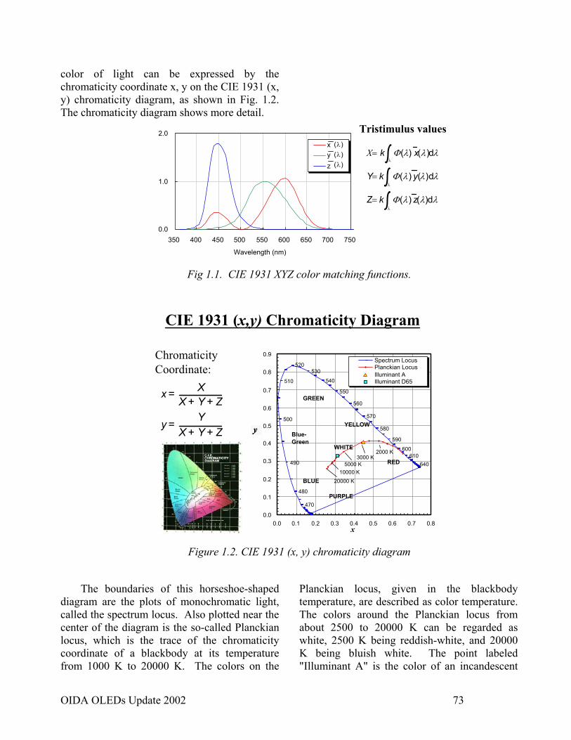
OIDA OLEDs Update 2002 73
color of light can be expressed by the chromaticity coordinate x, y on the CIE 1931 (x, y) chromaticity diagram, as shown in Fig. 1.2. The chromaticity diagram shows more detail.
0.0
1.0
2.0
350 400 450 500 550 600 650 700 750
Wavelength (nm)
x y z
(λ)(λ)
(λ) X= k Φ(λ) xλ
(λ)dλ
Y= k Φ(λ) yλ
(λ)dλ
Z= k Φ(λ) zλ
(λ)dλ
Tristimulus values
Fig 1.1. CIE 1931 XYZ color matching functions.
640610
600
590
580
570
560
550
540
530520
470
480
490
500
510
0.0
0.1
0.2
0.3
0.4
0.5
0.6
0.7
0.8
0.9
0.0 0.1 0.2 0.3 0.4 0.5 0.6 0.7 0.8x
Spectrum LocusPlanckian LocusIlluminant AIlluminant D65
2000 K3000 K
5000 K10000 K
20000 K
GREEN
Blue-Green
BLUE
YELLOW
WHITE
PURPLE
RED
CIE 1931 (x,y) Chromaticity Diagram
Chromaticity Coordinate:
x = X
X + Y + Z
y =Y
X + Y + Z
Figure 1.2. CIE 1931 (x, y) chromaticity diagram
The boundaries of this horseshoe-shaped diagram are the plots of monochromatic light, called the spectrum locus. Also plotted near the center of the diagram is the so-called Planckian locus, which is the trace of the chromaticity coordinate of a blackbody at its temperature from 1000 K to 20000 K. The colors on the
Planckian locus, given in the blackbody temperature, are described as color temperature. The colors around the Planckian locus from about 2500 to 20000 K can be regarded as white, 2500 K being reddish-white, and 20000 K being bluish white. The point labeled "Illuminant A" is the color of an incandescent
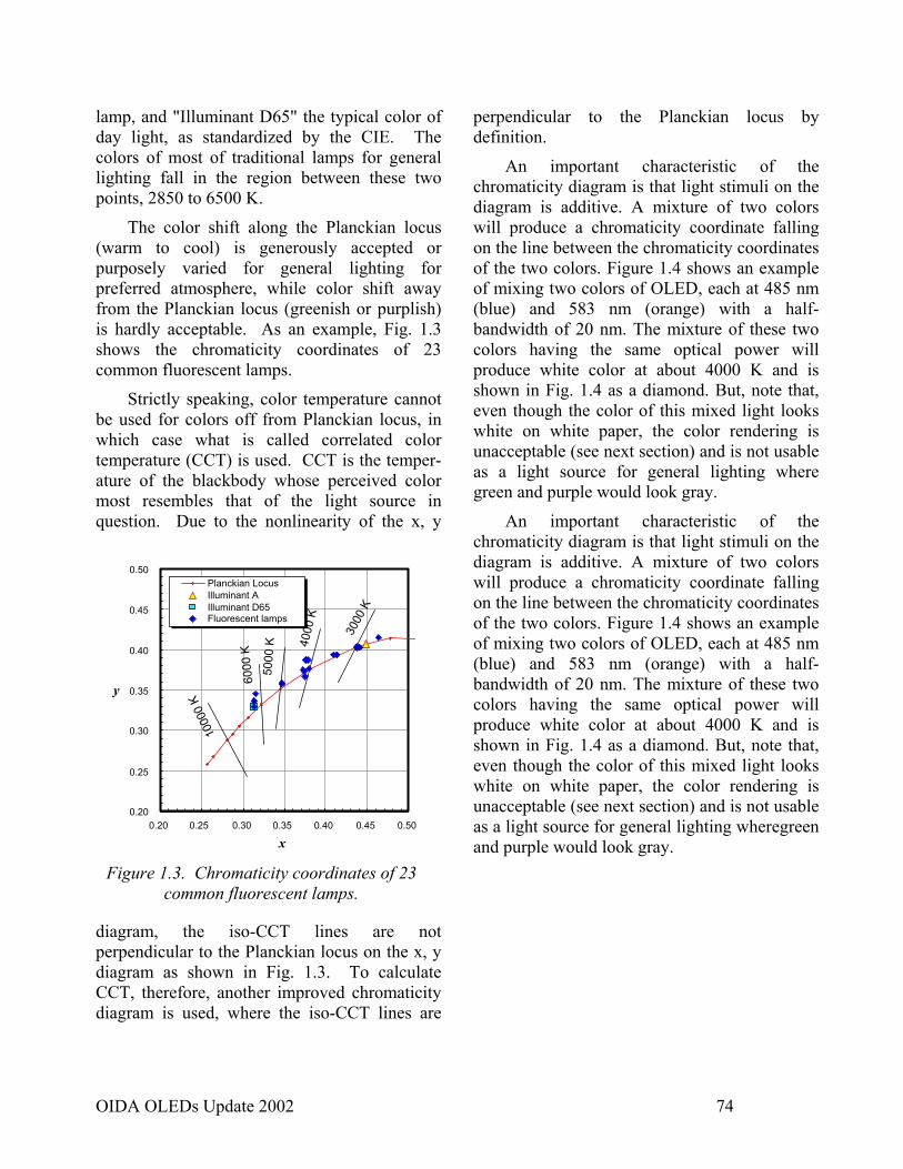
OIDA OLEDs Update 2002 74
lamp, and "Illuminant D65" the typical color of day light, as standardized by the CIE. The colors of most of traditional lamps for general lighting fall in the region between these two points, 2850 to 6500 K.
The color shift along the Planckian locus (warm to cool) is generously accepted or purposely varied for general lighting for preferred atmosphere, while color shift away from the Planckian locus (greenish or purplish) is hardly acceptable. As an example, Fig. 1.3 shows the chromaticity coordinates of 23 common fluorescent lamps.
Strictly speaking, color temperature cannot be used for colors off from Planckian locus, in which case what is called correlated color temperature (CCT) is used. CCT is the temper-ature of the blackbody whose perceived color most resembles that of the light source in question. Due to the nonlinearity of the x, y
diagram, the iso-CCT lines are not perpendicular to the Planckian locus on the x, y diagram as shown in Fig. 1.3. To calculate CCT, therefore, another improved chromaticity diagram is used, where the iso-CCT lines are
perpendicular to the Planckian locus by definition.
An important characteristic of the chromaticity diagram is that light stimuli on the diagram is additive. A mixture of two colors will produce a chromaticity coordinate falling on the line between the chromaticity coordinates of the two colors. Figure 1.4 shows an example of mixing two colors of OLED, each at 485 nm (blue) and 583 nm (orange) with a half- bandwidth of 20 nm. The mixture of these two colors having the same optical power will produce white color at about 4000 K and is shown in Fig. 1.4 as a diamond. But, note that, even though the color of this mixed light looks white on white paper, the color rendering is unacceptable (see next section) and is not usable as a light source for general lighting where green and purple would look gray.
An important characteristic of the chromaticity diagram is that light stimuli on the diagram is additive. A mixture of two colors will produce a chromaticity coordinate falling on the line between the chromaticity coordinates of the two colors. Figure 1.4 shows an example of mixing two colors of OLED, each at 485 nm (blue) and 583 nm (orange) with a half- bandwidth of 20 nm. The mixture of these two colors having the same optical power will produce white color at about 4000 K and is shown in Fig. 1.4 as a diamond. But, note that, even though the color of this mixed light looks white on white paper, the color rendering is unacceptable (see next section) and is not usable as a light source for general lighting wheregreen and purple would look gray.
0.20
0.25
0.30
0.35
0.40
0.45
0.50
0.20 0.25 0.30 0.35 0.40 0.45 0.50
x
y
Planckian LocusIlluminant AIlluminant D65Fluorescent lamps
3000
K
4000
K
5000
K
6000
K
1000
0 K
Figure 1.3. Chromaticity coordinates of 23 common fluorescent lamps.
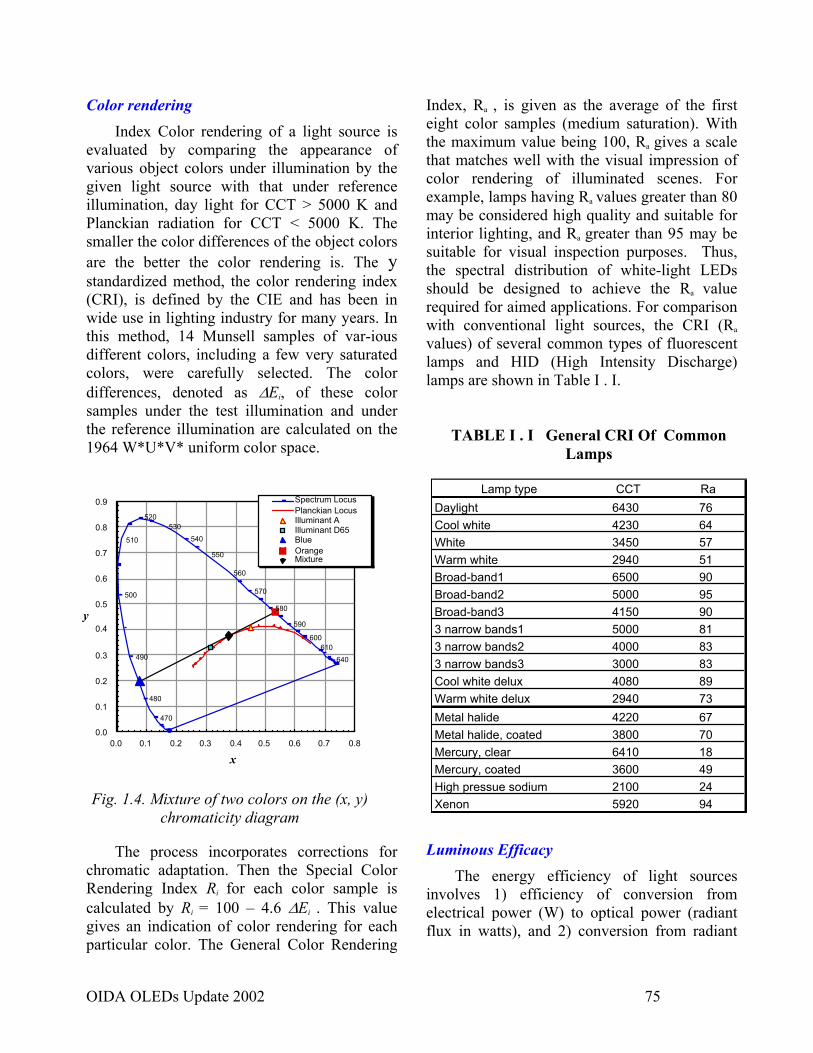
OIDA OLEDs Update 2002 75
Color rendering Index Color rendering of a light source is
evaluated by comparing the appearance of various object colors under illumination by the given light source with that under reference illumination, day light for CCT > 5000 K and Planckian radiation for CCT < 5000 K. The smaller the color differences of the object colors are the better the color rendering is. The y standardized method, the color rendering index (CRI), is defined by the CIE and has been in wide use in lighting industry for many years. In this method, 14 Munsell samples of var-ious different colors, including a few very saturated colors, were carefully selected. The color differences, denoted as ∆Ei, of these color samples under the test illumination and under the reference illumination are calculated on the 1964 W*U*V* uniform color space.
The process incorporates corrections for chromatic adaptation. Then the Special Color Rendering Index Ri for each color sample is calculated by Ri = 100 – 4.6 ∆Ei . This value gives an indication of color rendering for each particular color. The General Color Rendering
Index, Ra , is given as the average of the first eight color samples (medium saturation). With the maximum value being 100, Ra gives a scale that matches well with the visual impression of color rendering of illuminated scenes. For example, lamps having Ra values greater than 80 may be considered high quality and suitable for interior lighting, and Ra greater than 95 may be suitable for visual inspection purposes. Thus, the spectral distribution of white-light LEDs should be designed to achieve the Ra value required for aimed applications. For comparison with conventional light sources, the CRI (Ra values) of several common types of fluorescent lamps and HID (High Intensity Discharge) lamps are shown in Table I . I.
Luminous Efficacy
The energy efficiency of light sources involves 1) efficiency of conversion from electrical power (W) to optical power (radiant flux in watts), and 2) conversion from radiant
640
610600
590
580
570
560
550
540
530520
470
480
490
500
510
0.0
0.1
0.2
0.3
0.4
0.5
0.6
0.7
0.8
0.9
0.0 0.1 0.2 0.3 0.4 0.5 0.6 0.7 0.8
x
y
Spectrum LocusPlanckian LocusIlluminant AIlluminant D65BlueOrangeMixtureS
Fig. 1.4. Mixture of two colors on the (x, y) chromaticity diagram
Lamp type CCT RaDaylight 6430 76Cool white 4230 64White 3450 57Warm white 2940 51Broad-band1 6500 90Broad-band2 5000 95Broad-band3 4150 903 narrow bands1 5000 813 narrow bands2 4000 833 narrow bands3 3000 83Cool white delux 4080 89Warm white delux 2940 73Metal halide 4220 67Metal halide, coated 3800 70Mercury, clear 6410 18Mercury, coated 3600 49High pressue sodium 2100 24Xenon 5920 94
TABLE I . I General CRI Of Common Lamps
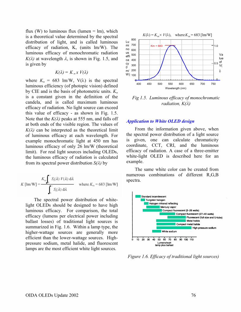
OIDA OLEDs Update 2002 76
flux (W) to luminous flux (lumen = lm), which is a theoretical value determined by the spectral distribution of light, and is called luminous efficacy of radiation, K, (units lm/W). The luminous efficacy of monochromatic radiation K(λ) at wavelength λ, is shown in Fig. 1.5, and is given by
K(λ) = K m x V(λ)
where Km = 683 lm/W, V(λ) is the spectral luminous efficiency (of photopic vision) defined by CIE and is the basis of photometric units. Km is a constant given in the definition of the candela, and is called maximum luminous efficacy of radiation. No light source can exceed this value of efficacy - as shown in Fig. 1.5. Note that the K(λ) peaks at 555 nm, and falls off at both ends of the visible region. The values of K(λ) can be interpreted as the theoretical limit of luminous efficacy at each wavelength. For example monochromatic light at 450 nm has luminous efficacy of only 26 lm/W (theoretical limit). For real light sources including OLEDs, the luminous efficacy of radiation is calculated from its spectral power distribution S(λ) by
The spectral power distribution of white-light OLEDs should be designed to have high luminous efficacy. For comparison, the total efficacy (lumens per electrical power including ballast losses) of traditional light sources is summarized in Fig. 1.6. Within a lamp type, the higher-wattage sources are generally more efficient than the lower-wattage sources. High-pressure sodium, metal halide, and fluorescent lamps are the most efficient white light sources.
Application to White OLED design From the information given above, when
the spectral power distribution of a light source is given, one can calculate chromaticity coordinate, CCT, CRI, and the luminous efficacy of radiation. A case of a three-emitter white-light OLED is described here for an example.
The same white color can be created from numerous combinations of different R,G,B spectra.
0
100
200
300
400
500
600
700
800
400 450 500 550 600 650 700 750Wavelength (nm)
1.0
0.5
0
Km = 683
K(λ) = Km × V (λ), whereKm = 683 [lm/W]
Luminousefficacy(lm/W)
ValueofV(λ)
Fig 1.5. Luminous efficacy of monochromatic radiation, K(λ)
Figure 1.6. Efficacy of traditional light sources)
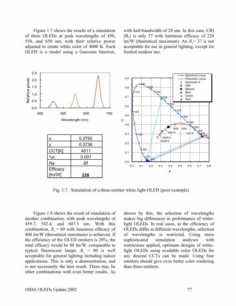
OIDA OLEDs Update 2002 77
Figure 1.7 shows the results of a simulation of three OLEDs at peak wavelengths of 450, 550, and 650 nm, with their relative power adjusted to create white color of 4000 K. Each OLED is a model using a Gaussian function,
with half-bandwidth of 20 nm. In this case, CRI (Ra) is only 37 with luminous efficacy of 228 lm/W (theoretical maximum). An Ra= 37 is not acceptable for use in general lighting, except for limited outdoor use.
Figure 1.8 shows the result of simulation of another combination, with peak wavelengths of 459.7, 542.4, and 607.3 nm. With this combination, Ra = 80 with luminous efficacy of 400 lm/W (theoretical maximum) is achieved. If the efficiency of the OLED emitters is 20%, the total efficacy would be 80 lm/W, comparable to typical fluorescent lamps. Ra = 80 is well acceptable for general lighting including indoor applications. This is only a demonstration, and is not necessarily the best result. There may be other combinations with even better results. As
shown by this, the selection of wavelengths makes big differences in performance of white-light OLEDs. In real cases, as the efficiency of OLEDs differ at different wavelengths, selection of wavelengths is restricted. Using more sophisticated simulation analyses with restrictions applied, optimum designs of white-light OLEDs using available color OLEDs for any desired CCTs can be made. Using four emitters should give even better color rendering than three emitters.
0.0
0.5
1.0
1.5
2.0
2.5
400 500 600 700
Wavelength (nm)
510
500
490
480
470
520530
540
550
560
570
580
590
600610
620
700640
0.0
0.1
0.2
0.3
0.4
0.5
0.6
0.7
0.8
0.9
0.0 0.1 0.2 0.3 0.4 0.5 0.6 0.7 0.8
x
y
Spectrum LocusPlanckian LocusIlluminant AD65MixtureBlueGreenRed
450
2000 3000 5000 K
10000 K20000 K
1000 K
x 0.3792y 0.3736CCT[K] 4011²uv 0.001Ra 37Efficacy [lm/W] 228
Fig. 1.7. Simulation of a three-emitter white light OLED (poor example)
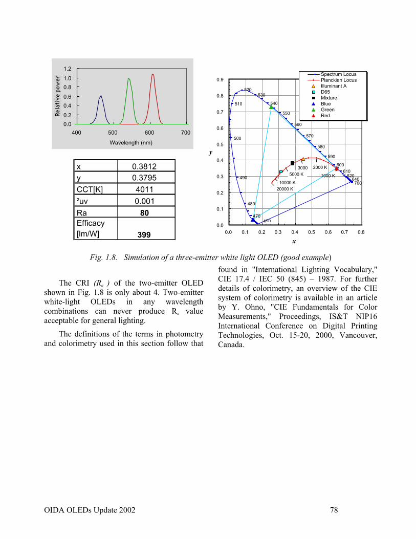
OIDA OLEDs Update 2002 78
The CRI (Ra ) of the two-emitter OLED shown in Fig. 1.8 is only about 4. Two-emitter white-light OLEDs in any wavelength combinations can never produce Ra value acceptable for general lighting.
The definitions of the terms in photometry and colorimetry used in this section follow that
found in "International Lighting Vocabulary," CIE 17.4 / IEC 50 (845) – 1987. For further details of colorimetry, an overview of the CIE system of colorimetry is available in an article by Y. Ohno, "CIE Fundamentals for Color Measurements," Proceedings, IS&T NIP16 International Conference on Digital Printing Technologies, Oct. 15-20, 2000, Vancouver, Canada.
0.00.2
0.40.6
0.81.0
1.2
400 500 600 700
Wavelength (nm)
640700
620610
600
590
580
570
560
550
540
530520
470
480
490
500
510
0.0
0.1
0.2
0.3
0.4
0.5
0.6
0.7
0.8
0.9
0.0 0.1 0.2 0.3 0.4 0.5 0.6 0.7 0.8
x
y
Spectrum LocusPlanckian LocusIlluminant AD65MixtureBlueGreenRed
450
2000 K3000 5000 K
20000 K
1000 K10000 K
x 0.3812y 0.3795CCT[K] 4011²uv 0.001Ra 80Efficacy [lm/W] 399
Fig. 1.8. Simulation of a three-emitter white light OLED (good example)