overvoltage & overcurrent protection ic & li+ charger ... · 1features applications...
TRANSCRIPT

1FEATURES
APPLICATIONS
DESCRIPTION
AC Adapter
VDC
GND1 Fm
1
2 7
5
4
6
8
bq24313bq24315
bq24080Charger IC
SYSTEM
IN OUT
VBAT
FAULT
CE
VS
S
ILIM
1 Fm
APPLICATION SCHEMATIC
bq24313bq24315
www.ti.com............................................................................................................................................... SLUS817A–MARCH 2008–REVISED NOVEMBER 2008
OVERVOLTAGE AND OVERCURRENT PROTECTION IC ANDLi+ CHARGER FRONT-END PROTECTION IC
• 5.5V LDO Mode Voltage Regulation23• Provides Protection for Three Variables: • Available in Space-Saving Small 8 Lead 2mm
×2mm SON– Input Overvoltage, with Rapid Response in< 1 µs
– User-Programmable Overcurrent with• Mobile Phones and Smart PhonesCurrent Limiting• PDAs– Battery Overvoltage• MP3 Players• 30V Maximum Input Voltage• Low-Power Handheld Devices• Supports up to 1.5A Input Current• Bluetooth™ Headsets
• Robust Against False Triggering Due toCurrent Transients
• Thermal Shutdown• Enable Input• Status Indication – Fault Condition
The bq24313 and bq24315 are highly integrated circuits designed to provide protection to Li-ion batteries fromfailures of the charging circuit. The IC continuously monitors the input voltage, the input current, and the batteryvoltage. The output acts as a linear regulator. The output is regulated to VO(REG) for inputs between VO(REG) andthe overvoltage threshold. If an input overvoltage condition occurs, the IC immediately removes power from thecharging circuit by turning off an internal switch. In the case of an overcurrent condition, it limits the systemcurrent at the threshold value, and if the overcurrent persists, switches the pass element OFF after a blankingperiod. Additionally, the IC also monitors its own die temperature and switches off if it exceeds 140°C. The inputovercurrent threshold is user-programmable.
The IC can be controlled by a processor and also provides status information about fault conditions to the host.
1
Please be aware that an important notice concerning availability, standard warranty, and use in critical applications of TexasInstruments semiconductor products and disclaimers thereto appears at the end of this data sheet.
2PowerPAD is a trademark of Texas Instruments.3Bluetooth is a trademark of Bluetooth SIG, Inc.
PRODUCTION DATA information is current as of publication date. Copyright © 2008, Texas Instruments IncorporatedProducts conform to specifications per the terms of the TexasInstruments standard warranty. Production processing does notnecessarily include testing of all parameters.
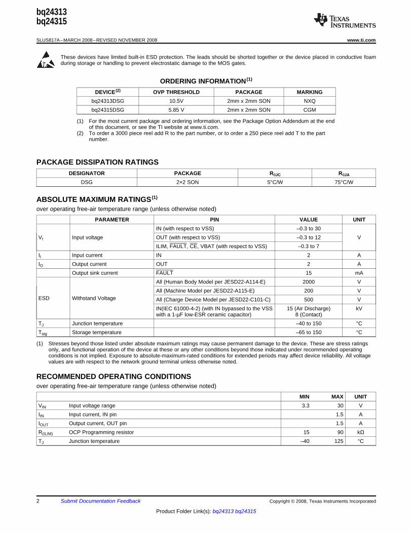
PACKAGE DISSIPATION RATINGS
ABSOLUTE MAXIMUM RATINGS (1)
RECOMMENDED OPERATING CONDITIONS
bq24313bq24315
SLUS817A–MARCH 2008–REVISED NOVEMBER 2008............................................................................................................................................... www.ti.com
These devices have limited built-in ESD protection. The leads should be shorted together or the device placed in conductive foamduring storage or handling to prevent electrostatic damage to the MOS gates.
ORDERING INFORMATION (1)
DEVICE (2) OVP THRESHOLD PACKAGE MARKINGbq24313DSG 10.5V 2mm x 2mm SON NXQbq24315DSG 5.85 V 2mm x 2mm SON CGM
(1) For the most current package and ordering information, see the Package Option Addendum at the endof this document, or see the TI website at www.ti.com.
(2) To order a 3000 piece reel add R to the part number, or to order a 250 piece reel add T to the partnumber.
DESIGNATOR PACKAGE RθJC RθJA
DSG 2×2 SON 5°C/W 75°C/W
over operating free-air temperature range (unless otherwise noted)
PARAMETER PIN VALUE UNITIN (with respect to VSS) –0.3 to 30
VI Input voltage OUT (with respect to VSS) –0.3 to 12 VILIM, FAULT, CE, VBAT (with respect to VSS) –0.3 to 7
II Input current IN 2 AIO Output current OUT 2 A
Output sink current FAULT 15 mAAll (Human Body Model per JESD22-A114-E) 2000 VAll (Machine Model per JESD22-A115-E) 200 V
ESD Withstand Voltage All (Charge Device Model per JESD22-C101-C) 500 VIN(IEC 61000-4-2) (with IN bypassed to the VSS 15 (Air Discharge) kVwith a 1-µF low-ESR ceramic capacitor) 8 (Contact)
TJ Junction temperature –40 to 150 °CTstg Storage temperature –65 to 150 °C
(1) Stresses beyond those listed under absolute maximum ratings may cause permanent damage to the device. These are stress ratingsonly, and functional operation of the device at these or any other conditions beyond those indicated under recommended operatingconditions is not implied. Exposure to absolute-maximum-rated conditions for extended periods may affect device reliability. All voltagevalues are with respect to the network ground terminal unless otherwise noted.
over operating free-air temperature range (unless otherwise noted)
MIN MAX UNITVIN Input voltage range 3.3 30 VIIN Input current, IN pin 1.5 AIOUT Output current, OUT pin 1.5 AR(ILIM) OCP Programming resistor 15 90 kΩTJ Junction temperature –40 125 °C
2 Submit Documentation Feedback Copyright © 2008, Texas Instruments Incorporated
Product Folder Link(s): bq24313 bq24315
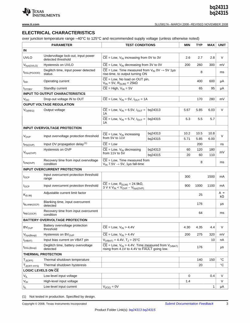
ELECTRICAL CHARACTERISTICS
bq24313bq24315
www.ti.com............................................................................................................................................... SLUS817A–MARCH 2008–REVISED NOVEMBER 2008
over junction temperature range –40°C to 125°C and recommended supply voltage (unless otherwise noted)
PARAMETER TEST CONDITIONS MIN TYP MAX UNITIN
Undervoltage lock-out, input powerUVLO CE = Low, VIN increasing from 0V to 3V 2.6 2.7 2.8 Vdetected thresholdVhys(UVLO) Hysteresis on UVLO CE = Low, VIN decreasing from 3V to 0V 200 260 300 mV
Deglitch time, input power detected CE = Low. Time measured from VIN 0V → 5V 1µstDGL(PGOOD) 8 msstatus rise-time, to output turning ONCE = Low, No load on OUT pin,IDD Operating current 400 600 µAVIN = 5V, R(ILIM) = 25kΩ
ISTDBY Standby current CE = High, VIN = 5V 65 95 µAINPUT TO OUTPUT CHARACTERISTICSVDO Drop-out voltage IN to OUT CE = Low, VIN = 5V, IOUT = 1A 170 280 mVOUPUT VOLTAGE REGULATIONVO(REG) Output voltage CE = Low, VIN = 6.5V, IOUT = bq24313 5.67 5.85 6.03 V
1ACE = Low, VIN = 5.7V, IOUT = bq24315 5.3 5.5 5.71A
INPUT OVERVOLTAGE PROTECTIONbq24313 10.2 10.5 10.8CE = Low, VIN increasingVOVP Input overvoltage protection threshold Vfrom 5V to 11V bq24315 5.71 5.85 6.00
tPD(OVP) Input OV propagation delay (1) CE = Low 200 nsHysteresis on OVP CE = Low, VIN decreasing bq24313 60 120 180
Vhys(OVP) mVfrom 11V to 5V bq24315 20 60 110Recovery time from input overvoltage CE = Low, Time measured fromtON(OVP) 8 mscondition VIN 7.5V → 5V, 1µs fall-time
INPUT OVERCURRENT PROTECTIONInput overcurrent protection thresholdIOCP 300 1500 mArange
CE = Low, R(ILIM) = 24.9kΩ,IOCP Input overcurrent protection threshold 900 1000 1100 mA3 V ≤ VIN < VOVP – Vhys(OVP)
Adjustable current limit factor A =K(ILIM) 25 kΩBlanking time, input overcurrenttBLANK(OCP) 176 µsdetectedRecovery time from input overcurrenttREC(OCP) 64 mscondition
BATTERY OVERVOLTAGE PROTECTIONBattery overvoltage protectionBVOVP CE = Low, VIN > 4.4V 4.30 4.35 4.4 Vthreshold
Vhys(Bovp) Hysteresis on BVOVP CE = Low, VIN > 4.4V 200 275 320 mVI(VBAT) Input bias current on VBAT pin V(VBAT) = 4.4V, TJ = 25°C 10 nA
Deglitch time, battery overvoltage CE = Low, VIN > 4.4V. Time measured from V(VBAT)tDGL(Bovp) 176 µsdetected rising from 4.1V to 4.4V to FAULT going low.THERMAL PROTECTIONTJ(OFF) Thermal shutdown temperature 140 150 °CTJ(OFF-HYS) Thermal shutdown hysteresis 20 °CLOGIC LEVELS ON CEVIL Low-level input voltage 0 0.4 VVIH High-level input voltage 1.4 VIIL Low-level input current V(/CE) = 0V 1 µA
(1) Not tested in production. Specified by design.
Copyright © 2008, Texas Instruments Incorporated Submit Documentation Feedback 3
Product Folder Link(s): bq24313 bq24315
bq24313bq24315
SLUS817A–MARCH 2008–REVISED NOVEMBER 2008............................................................................................................................................... www.ti.com
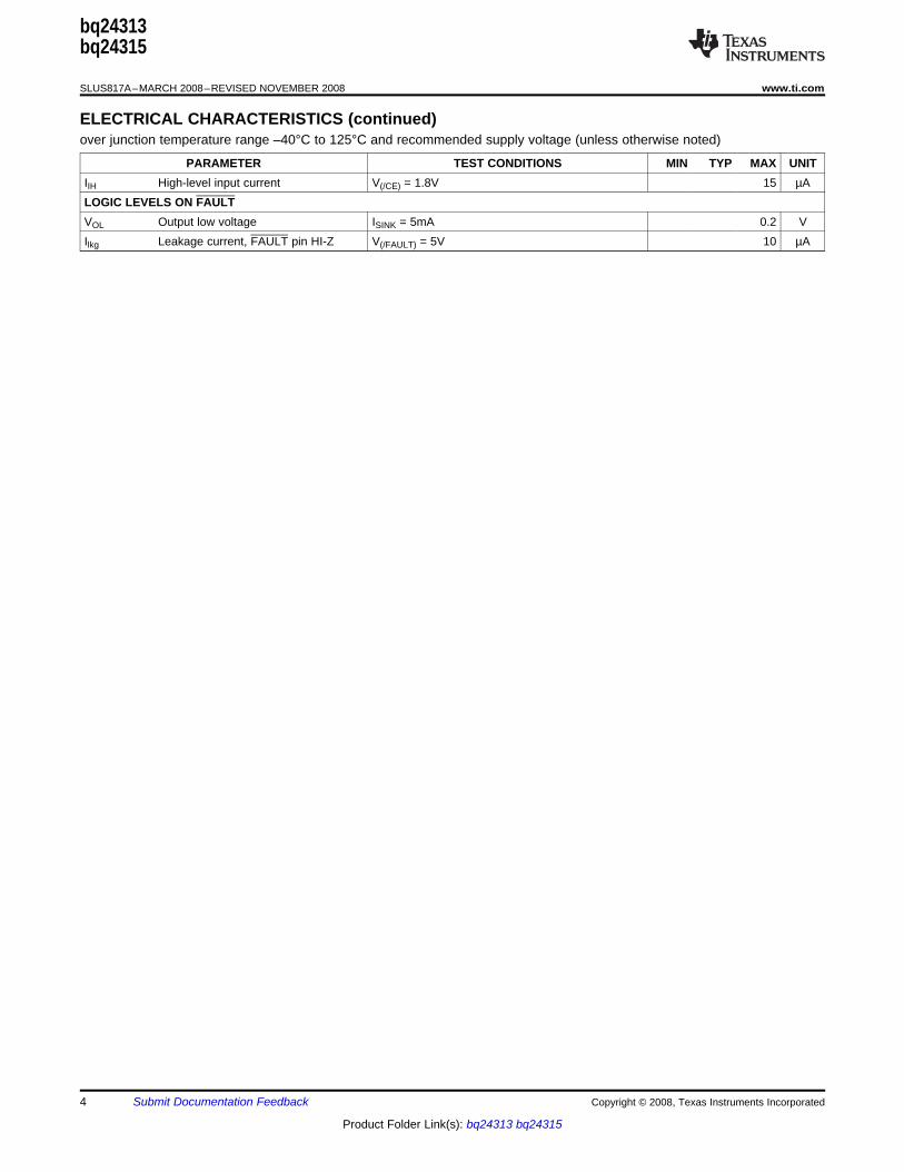
ELECTRICAL CHARACTERISTICS (continued)over junction temperature range –40°C to 125°C and recommended supply voltage (unless otherwise noted)
PARAMETER TEST CONDITIONS MIN TYP MAX UNITIIH High-level input current V(/CE) = 1.8V 15 µALOGIC LEVELS ON FAULTVOL Output low voltage ISINK = 5mA 0.2 VIlkg Leakage current, FAULT pin HI-Z V(/FAULT) = 5V 10 µA
4 Submit Documentation Feedback Copyright © 2008, Texas Instruments Incorporated
Product Folder Link(s): bq24313 bq24315

IN
OFF
Δ
Q1
OCP Comparator
Charge PumpBandgapBias Gen
ILIM
ILIMREF
OUT
CE
VBAT
COUNTERS,
CONTROL,
AND STATUS
THERMALSHUTDOWN
FAULT
VSS
OVP
UVLO
VIN
Current limitingloop
ILIMREF -
VBG
VISNS
VISNS
VBG
V
LoopO(REG)
tBLANK(OCP)
VBG
tDGL(PGOOD)
VIN
VBG VBG
tDGL(BOVP)
bq24313bq24315
www.ti.com............................................................................................................................................... SLUS817A–MARCH 2008–REVISED NOVEMBER 2008
Figure 1. Simplified Block Diagram
Copyright © 2008, Texas Instruments Incorporated Submit Documentation Feedback 5
Product Folder Link(s): bq24313 bq24315

TERMINAL FUNCTIONS
NC
VSS
FAULT
IN OUT
CE
1
2
3 6
8
7
4 5
VBAT
ILIM
bq24313bq24315
bq24313bq24315
SLUS817A–MARCH 2008–REVISED NOVEMBER 2008............................................................................................................................................... www.ti.com
TERMINALI/O DESCRIPTION
NAME DSGInput power. Connect IN to the external DC supply. Bypass IN to VSS with a 1µF ceramic capacitorIN 1 I (minimum).
VSS 2 – Ground terminalThis pin may have internal circuits used for test purposes. Do not make any external connection to thisNC 3 pin for normal operation.Open-drain, device status output. FAULT = Low indicates that the input FET Q1 is off due to input
FAULT 4 O overvoltage, input overcurrent, battery overvoltage, or thermal shutdown. FAULT is high impedanceduring normal operation. Connect a pullup resistor from FAULT to the desired logic level voltage rail.
5 I Chip enable active low input. Connect CE = High to disable the IC and turn the input FET off. ConnectCE CE = low for normal operation. CE is internally pulled down.VBAT 6 I Battery voltage sense input. Connect to the battery pack positive terminal through a resistor.
Input overcurrent threshold programming. Connect a resistor from ILIM to VSS to set the overcurrentILIM 7 I/O threshold.8 O Output terminal to the charging system. Connect OUT to the external load circuitry. Bypass OUT to VSSOUT with a 1µF ceramic capacitor (minimum).
There is an internal electrical connection between the exposed thermal pad and the VSS pin of thedevice. The thermal pad must be connected to the same potential as the VSS pin on the printed circuitThermal PAD – board. Do not use the thermal pad as the primary ground input for the device. The VSS pin must beconnected to ground at all times.
DSG Package(Top View)
6 Submit Documentation Feedback Copyright © 2008, Texas Instruments Incorporated
Product Folder Link(s): bq24313 bq24315

TYPICAL OPERATING PERFORMANCE
VIN
VOUT
IIN
5 V/div
200 mV/div
200 mA/div
t - Time - 2 ms/div
V = 0 V to 9 V,
t = 50 s
IN
r m
VIN
VOUT
IIN
2 V/div
2 V/div
200 mA/div
t - Time - 2 ms/div
R = 6.6OUT
W
VIN
VOUT
t - Time - 10 s/divm
5 V/div
2 V/div
V = 5 V to 12 V stepIN
VIN
VOUT
5 V/div
2 V/div
t - Time - 20 s/divm
V = 5 V to 12 V,
t = 20 s
IN
r m
5 V/div
1 V/div
500 mA/div
VIN
VOUT
IIN
t - Time - 200 ms/div
VFAULT
1 V/div
VIN
VOUT
2 V/div
2 V/div
t - Time - 4 ms/div
V = 7.5 V to 5 V,
t = 1.2 msIN
r
bq24313bq24315
www.ti.com............................................................................................................................................... SLUS817A–MARCH 2008–REVISED NOVEMBER 2008
Test conditions (unless otherwise noted) for typical operating performance: VIN = 5 V, CIN = 1 µF, COUT = 1 µF,R(ILIM) = 25 kΩ, RBAT = 100 kΩ, TA = 25°C, VPU = 3.3V (see Figure 22 for the Typical Application Circuit)
NORMAL POWER-ON SHOWING SOFT-START OVP AT POWER-ON
Figure 2. Figure 3.
OVP RESPONSE FOR INPUT STEP OVP RESPONSE FOR INPUT STEP
Figure 4. Figure 5.
OCP, POWERING UP INTO A SHORT CIRCUIT ONOUT,COUNTER COUNTS TO 15 BEFORE SWITCHING OFF
RECOVERY FROM OVP THE DEVICE
Figure 6. Figure 7.
Copyright © 2008, Texas Instruments Incorporated Submit Documentation Feedback 7
Product Folder Link(s): bq24313 bq24315

2 V/div
1 V/div
500 mA/div
VIN
VOUT
IIN
t - Time - 2 ms/div
VFAULT
VOUT
IIN
2 V/div
1 V/div
500 mA/div
t - Time - 40 s/divm
2 V/div
1 V/divV
BAT
VOUT
t - Time - 100 s/divm
VFAULT
1 V/div
2 V/div
2 V/div
200 mA/div
VOUT
t - Time - 4 ms/div
VBAT
VFAULT
2 V/div
2 V/div
VIN
t - Time - 40 ms/div
VOUT
2.4
2.45
2.5
2.55
2.6
2.65
2.7
2.75
-50 -30 -10 10 30 50 70 90 110 130
V IncreasingIN
V DecreasingIN
Temperature - C°
V, V
- V
UV
LO
HY
S-U
VL
O
bq24313bq24315
SLUS817A–MARCH 2008–REVISED NOVEMBER 2008............................................................................................................................................... www.ti.com
TYPICAL OPERATING PERFORMANCE (continued)
ROUT SWITCHES FROM 6.6Ω TO 3.3Ω,SHOWS CURRENTOCP, ZOOM-IN ON THE FIRST CYCLE OF FIGURE 7 LIMITING AND SOFT-STOP
Figure 8. Figure 9.
BAT-OVP, V(VBAT) STEPS FROM 4 V TO 4.5 V,SHOWS BAT-OVP, V(VBAT) CYCLES BETWEEN 4 V AND 4.5tDGL(BAT-OVP) AND SOFT STOP V,SHOWS BAT-OVP COUNTER
Figure 10. Figure 11.
UNDERVOLTAGE LOCKOUTINPUT VOLTAGE RAMP-UP / RAMP-DOWN vs
bq24313 FREE-AIR TEMPERATURE
Figure 12. Figure 13.
8 Submit Documentation Feedback Copyright © 2008, Texas Instruments Incorporated
Product Folder Link(s): bq24313 bq24315
100
120
140
160
180
200
220
240
260
280
0 50 100 150
V = 4 VIN
VD
O@
1A
- m
V
Temperature - C°
V = 5 VIN
10.3
10.35
10.4
10.45
10.5
10.55
-50 -30 -10 10 30 50 70 90 110 130Temperature °C
V,
V-
VO
VP
HY
S-O
VP
V DecreasingIN
V IncreasingIN
0
200
400
600
800
1000
1200
1400
1600
0 10 20 30 40 50 60 70 80 90 100
I-
mA
OC
P
R - kILIM
W
5.78
5.8
5.82
5.84
5.86
5.88
-50 -30 -10 10 30 50 70 90 110 130
V IncreasingIN
V DecreasingIN
Temperature - C°
V,
V-
VO
VP
HY
S-O
VP
bq24313bq24315
www.ti.com............................................................................................................................................... SLUS817A–MARCH 2008–REVISED NOVEMBER 2008
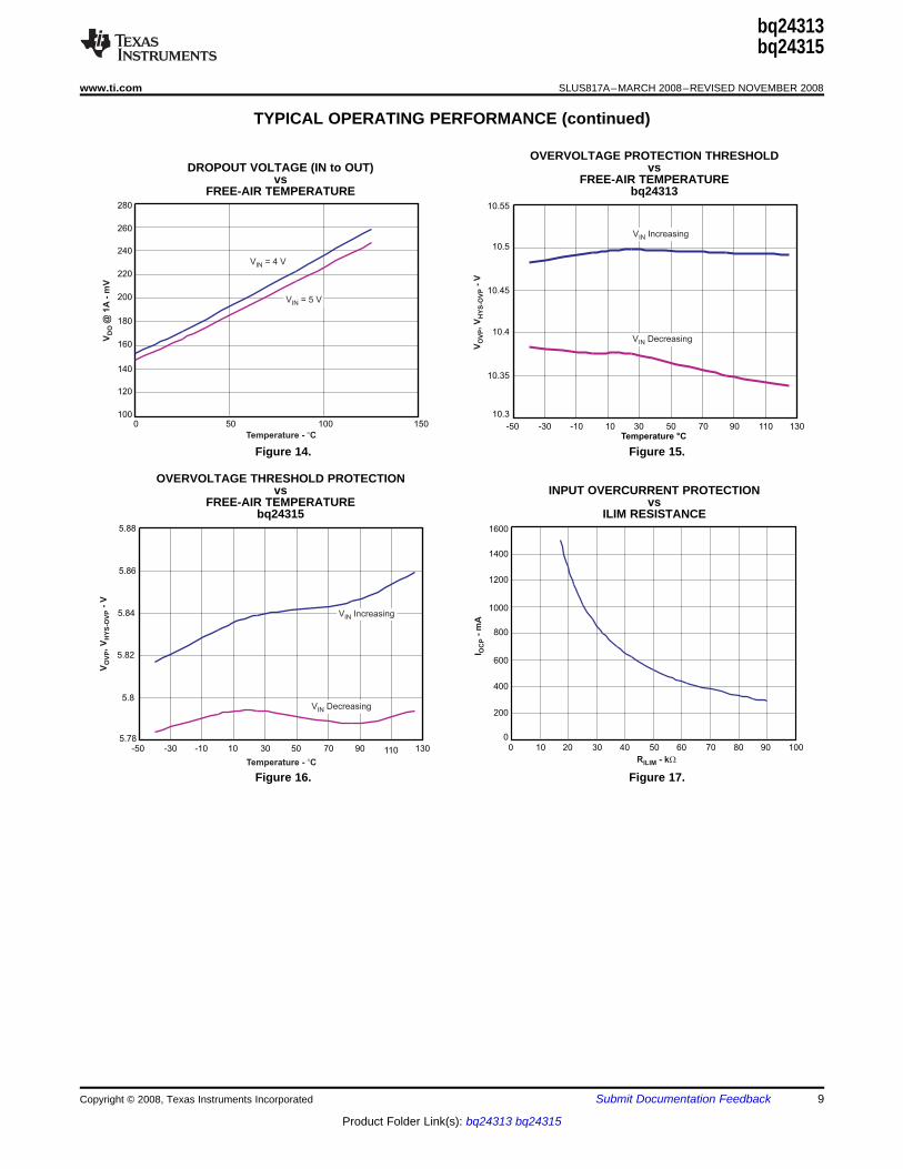
TYPICAL OPERATING PERFORMANCE (continued)
OVERVOLTAGE PROTECTION THRESHOLDDROPOUT VOLTAGE (IN to OUT) vs
vs FREE-AIR TEMPERATUREFREE-AIR TEMPERATURE bq24313
Figure 14. Figure 15.
OVERVOLTAGE THRESHOLD PROTECTIONvs INPUT OVERCURRENT PROTECTION
FREE-AIR TEMPERATURE vsbq24315 ILIM RESISTANCE
Figure 16. Figure 17.
Copyright © 2008, Texas Instruments Incorporated Submit Documentation Feedback 9
Product Folder Link(s): bq24313 bq24315

4.05
4.1
4.15
4.2
4.25
4.3
4.35
4.4
-50 -30 -10 10 30 50 70 90 110 130
BV (V Increasing)OVP VBAT
Bat-OVP Recovery (V Decreasing)VBAT
BV
- V
OV
P
Temperature - C°
975
976
977
978
979
980
981
982
983
984
985
-50 -30 -10 10 30 50 70 90 110 130
I-
mA
OC
P
Temperature - C°
0
100
200
300
400
500
600
700
800
900
0 5 10 15 20 25 30 35
I ( = Low)DD CE
I ( = High)STDBY CE
I, I
-A
DD
ST
DB
Ym
V - VIN
0
0.5
1
1.5
2
2.5
-50 -30 -10 10 30 50 70 90 110 130
Temperature - C°
I-
nA
VB
AT
bq24313bq24315
SLUS817A–MARCH 2008–REVISED NOVEMBER 2008............................................................................................................................................... www.ti.com
TYPICAL OPERATING PERFORMANCE (continued)
INPUT OVERCURRENT PROTECTION BATTERY OVERVOLTAGE PROTECTIONvs vs
FREE-AIR TEMPERATURE FREE-AIR TEMPERATURE
Figure 18. Figure 19.
LEAKAGE CURRENT (VBAT Pin) SUPPLY CURRENTvs vs
FREE-AIR TEMPERATURE INPUT VOLTAGE
Figure 20. Figure 21.
10 Submit Documentation Feedback Copyright © 2008, Texas Instruments Incorporated
Product Folder Link(s): bq24313 bq24315
TYPICAL APPLICATION CIRCUIT
AC Adapter
VDC
GND
CIN
1
7 2
5
4
6
8
bq24313bq24315
bq24080Charger IC
SYSTEM
IN OUT
VBAT
FAULT
CE
VS
S
ILIM
COUT
COUT
RBAT
RCE
HostController
RFAULT
VPU
RPU
1 Fm1 Fm
100 kW
47 kW
47 kW
47 kW
RILM
DETAILED FUNCTIONAL DESCRIPTION
POWER DOWN
POWER-ON RESET
OPERATION
bq24313bq24315
www.ti.com............................................................................................................................................... SLUS817A–MARCH 2008–REVISED NOVEMBER 2008
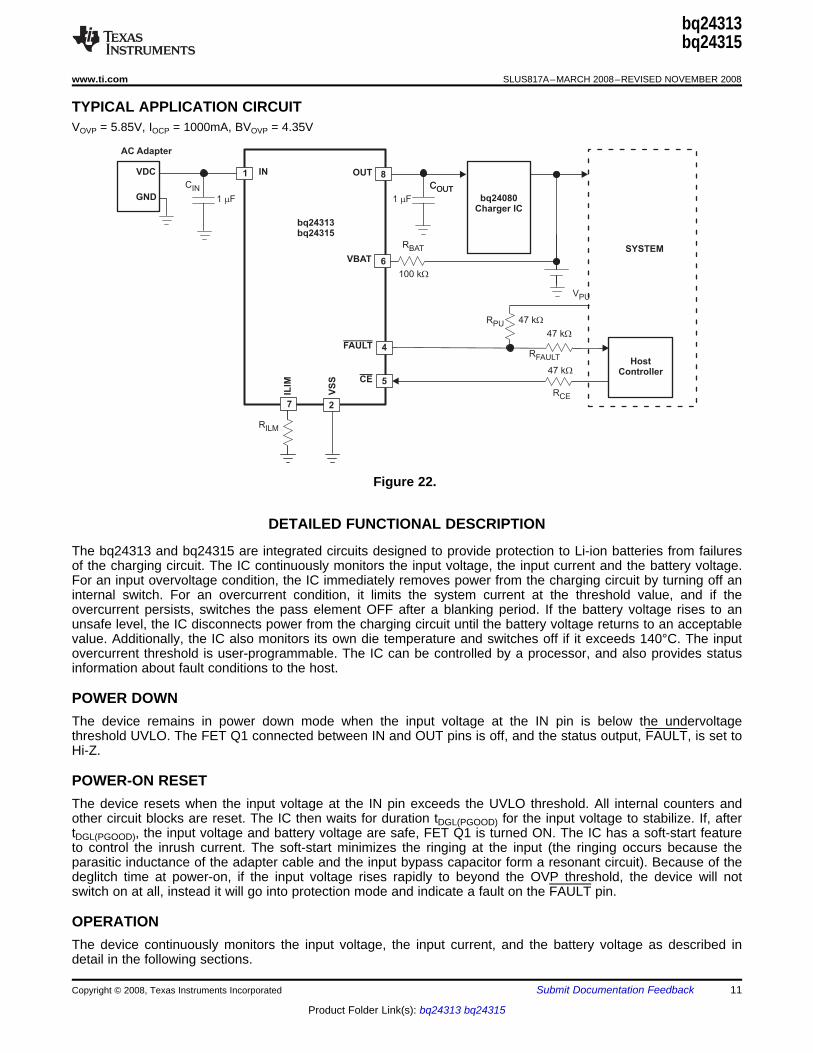
VOVP = 5.85V, IOCP = 1000mA, BVOVP = 4.35V
Figure 22.
The bq24313 and bq24315 are integrated circuits designed to provide protection to Li-ion batteries from failuresof the charging circuit. The IC continuously monitors the input voltage, the input current and the battery voltage.For an input overvoltage condition, the IC immediately removes power from the charging circuit by turning off aninternal switch. For an overcurrent condition, it limits the system current at the threshold value, and if theovercurrent persists, switches the pass element OFF after a blanking period. If the battery voltage rises to anunsafe level, the IC disconnects power from the charging circuit until the battery voltage returns to an acceptablevalue. Additionally, the IC also monitors its own die temperature and switches off if it exceeds 140°C. The inputovercurrent threshold is user-programmable. The IC can be controlled by a processor, and also provides statusinformation about fault conditions to the host.
The device remains in power down mode when the input voltage at the IN pin is below the undervoltagethreshold UVLO. The FET Q1 connected between IN and OUT pins is off, and the status output, FAULT, is set toHi-Z.
The device resets when the input voltage at the IN pin exceeds the UVLO threshold. All internal counters andother circuit blocks are reset. The IC then waits for duration tDGL(PGOOD) for the input voltage to stabilize. If, aftertDGL(PGOOD), the input voltage and battery voltage are safe, FET Q1 is turned ON. The IC has a soft-start featureto control the inrush current. The soft-start minimizes the ringing at the input (the ringing occurs because theparasitic inductance of the adapter cable and the input bypass capacitor form a resonant circuit). Because of thedeglitch time at power-on, if the input voltage rises rapidly to beyond the OVP threshold, the device will notswitch on at all, instead it will go into protection mode and indicate a fault on the FAULT pin.
The device continuously monitors the input voltage, the input current, and the battery voltage as described indetail in the following sections.
Copyright © 2008, Texas Instruments Incorporated Submit Documentation Feedback 11
Product Folder Link(s): bq24313 bq24315

Input Overvoltage Protection
Input Overcurrent Protection
Battery Overvoltage Protection
Thermal Protection
Enable Function
Fault Indication
bq24313bq24315
SLUS817A–MARCH 2008–REVISED NOVEMBER 2008............................................................................................................................................... www.ti.com
While the input voltage is less than VO(REG), the output voltage tracks the input voltage (less the drop due to theRDS(on) of Q1). When the input voltage is between VO(REG) and VOVP, the device functions as a linear regulatorand regulates the output voltage to 5.5V. If the input voltage rises above VOVP, the internal FET Q1 is turned off,removing power to the output. The response is rapid, with the FET turning off in less than a microsecond. TheFAULT pin is driven low. When the input voltage returns below VOVP – Vhys(OVP) (but is still above UVLO), theFET Q1 is turned on again after a deglitch time of tON(OVP) to ensure that the input supply has stabilized.
The overcurrent threshold is programmed by a resistor R(ILIM) connected from the ILIM pin to VSS. Figure 17shows the OCP threshold as a function of R(ILIM), and may be approximated by the following equation:IOCP = 25 ÷ R(ILIM) (current in A, resistance in kΩ)
If the load current tries to exceed the IOCP threshold, the device limits the current for a blanking duration oftBLANK(OCP). If the load current returns to less than IOCP before tBLANK(OCP) times out, the device continues tooperate. However, if the overcurrent situation persists for tBLANK(OCP), the FET Q1 is turned off for a duration oftREC(OCP), and the FAULT pin is driven low. The FET is then turned on again after tREC(OCP) and the current ismonitored all over again. Each time an OCP fault occurs, an internal counter is incremented. If 15 OCP faultsoccur in one charge cycle, the FET is turned off permanently. The counter is cleared either by removing andre-applying input power, or by disabling and re-enabling the device with the CE pin.
To prevent the input voltage from spiking up due to the inductance of the input cable, Q1 is turned off slowly,resulting in a “soft-stop”.
The battery overvoltage threshold BVOVP is internally set to 4.35V. If the battery voltage exceeds the BVOVPthreshold, the FET Q1 is turned off, and the FAULT pin is driven low. The FET is turned back on once the batteryvoltage drops to BVOVP – Vhys(Bovp). Each time a battery overvoltage fault occurs, an internal counter isincremented. If 15 such faults occur in one charge cycle, the FET is turned off permanently. The counter iscleared either by removing and re-applying input power, or by disabling and re-enabling the device with the CEpin. For a battery overvoltage fault, Q1 is gradually switched OFF.
If the junction temperature of the device exceeds TJ(OFF), the FET Q1 is turned off, and the FAULT pin is drivenlow. The FET is turned back on when the junction temperature falls below TJ(OFF) – TJ(OFF-HYS).
The IC has an enable pin which can be used to enable or disable the device. When the CE pin is driven high, theinternal FET is turned off. When the CE pin is low, the FET is turned on if other conditions are safe. The OCPcounter and the Bat-OVP counter are both reset when the device is disabled and re-enabled. The CE pin has aninternal pulldown resistor and can be left floating. Note that the FAULT pin functionality is also disabled when theCE pin is high.
The FAULT pin is an active-low open-drain output. It is in a high-impedance state when operating conditions aresafe, or when the device is disabled by setting CE high. With CE low, the FAULT pin goes low whenever any ofthese events occurs:• Input overvoltage• Input overcurrent• Battery overvoltage• IC Overtemperature
12 Submit Documentation Feedback Copyright © 2008, Texas Instruments Incorporated
Product Folder Link(s): bq24313 bq24315
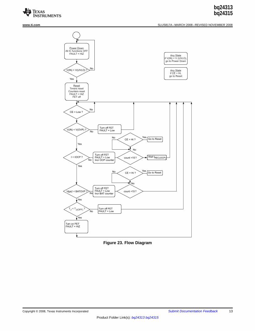
V(IN) > V(UVLO) ?No
CE = Low ?No
V(IN) < V(OVP) ?
Yes
No
Turn off FETFAULT = Low
I < IOCP ?
Yes
No
Wait tREC(OCP)
VBAT < BATOVP ?
Yes
No
Turn on FETFAULT = HiZ
Turn off FETFAULT = LowIncr OCP counter
count <15?
CE = Hi ?No
No
Go to ResetYes
Turn off FETFAULT = LowIncr BAT counter
count <15 ?
CE = Hi ? Go to ResetYes
No
No
Yes
Yes
NoTurn off FETFAULT = Low
Power DownAll IC functions OFF
FAULT = HiZ
ResetTimers reset
Counters resetFAULT = HiZ
FET off
T < T ?J J(OFF)
Any Stateif V(IN) < V (UVLO),go to Power Down
Any Stateif CE = Hi,
go to Reset
bq24313bq24315
www.ti.com............................................................................................................................................... SLUS817A–MARCH 2008–REVISED NOVEMBER 2008
Figure 23. Flow Diagram
Copyright © 2008, Texas Instruments Incorporated Submit Documentation Feedback 13
Product Folder Link(s): bq24313 bq24315
APPLICATION INFORMATION (WITH REFERENCE TO FIGURE 22)
Selection of RBAT
Selection of RCE, RFAULT, and RPU
Selection of Input and Output Bypass Capacitors
Powering Accessories
bq24313bq24315
SLUS817A–MARCH 2008–REVISED NOVEMBER 2008............................................................................................................................................... www.ti.com
It is strongly recommended that the battery not be tied directly to the VBAT pin of the device, as under somefailure modes of the IC, the voltage at the IN pin may appear on the VBAT pin. This voltage can be as high as30V, and applying 30V to the battery in case of the failure of the bq24315 can be hazardous. Connecting theVBAT pin through RBAT prevents a large current from flowing into the battery in case of a failure of the IC. In theinterests of safety, RBAT should have a high value. The problem with a large RBAT is that the voltage drop acrossthis resistor, due to the VBAT bias current I(VBAT), causes an error in the BVOVP threshold. This error is over andabove the tolerance on the nominal 4.35V BVOVP threshold.
Choosing RBAT in the range 100kΩ to 470kΩ is a good compromise. In the event of an IC failure, with RBAT equalto 100kΩ, the maximum current flowing into the battery would be (30V – 3V) ÷ 100kΩ = 246µA, which is lowenough to be absorbed by the bias currents of the system components. RBAT equal to 100kΩ results in aworst-case voltage drop of RBAT × I(VBAT) = 1mV. This is negligible to compared to the internal tolerance of 50mVon BVOVP threshold.
If the Bat-OVP function is not required, the VBAT pin should be connected to VSS.
The CE pin can be used to enable and disable the IC. If host control is not required, the CE pin can be tied toground or left un-connected, permanently enabling the device.
In applications where external control is required, the CE pin can be controlled by a host processor. As in thecase of the VBAT pin (see above), the CE pin should be connected to the host GPIO pin through as large aresistor as possible. The limitation on the resistor value is that the minimum VOH of the host GPIO pin less thedrop across the resistor should be greater than VIH of the bq24315 CE pin. The drop across the resistor is givenby RCE × IIH.
The FAULT pin is an open-drain output that goes low during OV, OC, battery-OV, and OT events. If theapplication does not require monitoring of the FAULT pin, it can be left unconnected. But if the FAULT pin has tobe monitored, it should be pulled high externally through RPU, and connected to the host through RFAULT. RFAULTprevents damage to the host controller if the bq24315 fails (see above). The resistors should be of high value, inpractice values between 22kΩ and 100kΩ should be sufficient.
The input capacitor CIN in Figure 22 is for decoupling, and serves an important purpose. Whenever there is astep change downwards in the system load current, the inductance of the input cable causes the input voltage tospike up. CIN prevents the input voltage from overshooting to dangerous levels. It is recommended that a ceramiccapacitor of at least 1µF be used at the input of the device. It should be located in close proximity to the IN pin.
COUT in Figure 22 is also important: If a fast (< 1µs rise time) overvoltage transient occurs at the input, thecurrent that charges COUT causes the device’s current-limiting loop to start, reducing the gate-drive to FET Q1.This results in improved performance for input overvoltage protection. COUT should also be a ceramic capacitor ofat least 1µF, located close to the OUT pin. COUT also serves as the input decoupling capacitor for the chargingcircuit downstream of the protection IC.
In some applications, the equipment that the protection IC resides in may be required to provide power to anaccessory (e.g. a cellphone may power a headset or an external memory card) through the same connector pinsthat are used by the adapter for charging. Figure 24 and Figure 25 illustrate typical charging andaccessory-powering scenarios:
14 Submit Documentation Feedback Copyright © 2008, Texas Instruments Incorporated
Product Folder Link(s): bq24313 bq24315

IN OUTCharger
Accessory
power supply
EN
DIS
Batterypack
to rest of
system
e.g.
cellphone
AC Adapterbq24313bq24315
IN OUTCharger
Accessory
power supply
EN
DIS Battery
pack
to rest of
system
e.g.
cellphone
bq24313bq24315
PCB Layout Guidelines:
bq24313bq24315
www.ti.com............................................................................................................................................... SLUS817A–MARCH 2008–REVISED NOVEMBER 2008
Figure 24. Charging - The Red Arrows Show the Direction of Current Flow
Figure 25. Powering an Accessory - The Red Arrows Show the Direction of Current Flow
In the second case, when power is being delivered to an accessory, the bq24313/bq24315 device is required tosupport current flow from the OUT pin to the IN pin.
If VOUT > UVLO + 0.7V, FET Q1 is turned on, and the reverse current does not flow through the diode butthrough Q1. Q1 remains ON as long as VOUT > UVLO – Vhys(UVLO) + RDS(on) × I(ACCESSORY). Within this voltagerange, the reverse current capability is the same as the forward capability, 1.5A. It should be noted that there isno overcurrent protection in this direction.
• This device is a protection device, and is meant to protect down-stream circuitry from hazardous voltages.Potentially, high voltages may be applied to this IC. It has to be ensured that the edge-to-edge clearances ofPCB traces satisfy the design rules for high voltages.
• The device uses SON packages with a PowerPAD™. For good thermal performance, the PowerPAD shouldbe thermally coupled with the PCB ground plane. In most applications, this will require a copper pad directlyunder the IC. This copper pad should be connected to the ground plane with an array of thermal vias.
• CIN and COUT should be located close to the IC. Other components like R(ILIM) and RBAT should also belocated close to the IC.
Copyright © 2008, Texas Instruments Incorporated Submit Documentation Feedback 15
Product Folder Link(s): bq24313 bq24315

PACKAGE OPTION ADDENDUM
www.ti.com 10-Jun-2014
Addendum-Page 1
PACKAGING INFORMATION
Orderable Device Status(1)
Package Type PackageDrawing
Pins PackageQty
Eco Plan(2)
Lead/Ball Finish(6)
MSL Peak Temp(3)
Op Temp (°C) Device Marking(4/5)
Samples
BQ24313DSGR ACTIVE WSON DSG 8 3000 Green (RoHS& no Sb/Br)
CU NIPDAU Level-2-260C-1 YEAR -40 to 125 NXQ
BQ24313DSGT ACTIVE WSON DSG 8 250 Green (RoHS& no Sb/Br)
CU NIPDAU Level-2-260C-1 YEAR -40 to 125 NXQ
BQ24315DSGR ACTIVE WSON DSG 8 3000 Green (RoHS& no Sb/Br)
CU NIPDAU Level-2-260C-1 YEAR -40 to 125 CGM
BQ24315DSGT ACTIVE WSON DSG 8 250 Green (RoHS& no Sb/Br)
CU NIPDAU Level-2-260C-1 YEAR -40 to 125 CGM
(1) The marketing status values are defined as follows:ACTIVE: Product device recommended for new designs.LIFEBUY: TI has announced that the device will be discontinued, and a lifetime-buy period is in effect.NRND: Not recommended for new designs. Device is in production to support existing customers, but TI does not recommend using this part in a new design.PREVIEW: Device has been announced but is not in production. Samples may or may not be available.OBSOLETE: TI has discontinued the production of the device.
(2) Eco Plan - The planned eco-friendly classification: Pb-Free (RoHS), Pb-Free (RoHS Exempt), or Green (RoHS & no Sb/Br) - please check http://www.ti.com/productcontent for the latest availabilityinformation and additional product content details.TBD: The Pb-Free/Green conversion plan has not been defined.Pb-Free (RoHS): TI's terms "Lead-Free" or "Pb-Free" mean semiconductor products that are compatible with the current RoHS requirements for all 6 substances, including the requirement thatlead not exceed 0.1% by weight in homogeneous materials. Where designed to be soldered at high temperatures, TI Pb-Free products are suitable for use in specified lead-free processes.Pb-Free (RoHS Exempt): This component has a RoHS exemption for either 1) lead-based flip-chip solder bumps used between the die and package, or 2) lead-based die adhesive used betweenthe die and leadframe. The component is otherwise considered Pb-Free (RoHS compatible) as defined above.Green (RoHS & no Sb/Br): TI defines "Green" to mean Pb-Free (RoHS compatible), and free of Bromine (Br) and Antimony (Sb) based flame retardants (Br or Sb do not exceed 0.1% by weightin homogeneous material)
(3) MSL, Peak Temp. - The Moisture Sensitivity Level rating according to the JEDEC industry standard classifications, and peak solder temperature.
(4) There may be additional marking, which relates to the logo, the lot trace code information, or the environmental category on the device.
(5) Multiple Device Markings will be inside parentheses. Only one Device Marking contained in parentheses and separated by a "~" will appear on a device. If a line is indented then it is a continuationof the previous line and the two combined represent the entire Device Marking for that device.
(6) Lead/Ball Finish - Orderable Devices may have multiple material finish options. Finish options are separated by a vertical ruled line. Lead/Ball Finish values may wrap to two lines if the finishvalue exceeds the maximum column width.

PACKAGE OPTION ADDENDUM
www.ti.com 10-Jun-2014
Addendum-Page 2
Important Information and Disclaimer:The information provided on this page represents TI's knowledge and belief as of the date that it is provided. TI bases its knowledge and belief on informationprovided by third parties, and makes no representation or warranty as to the accuracy of such information. Efforts are underway to better integrate information from third parties. TI has taken andcontinues to take reasonable steps to provide representative and accurate information but may not have conducted destructive testing or chemical analysis on incoming materials and chemicals.TI and TI suppliers consider certain information to be proprietary, and thus CAS numbers and other limited information may not be available for release.
In no event shall TI's liability arising out of such information exceed the total purchase price of the TI part(s) at issue in this document sold by TI to Customer on an annual basis.

TAPE AND REEL INFORMATION
*All dimensions are nominal
Device PackageType
PackageDrawing
Pins SPQ ReelDiameter
(mm)
ReelWidth
W1 (mm)
A0(mm)
B0(mm)
K0(mm)
P1(mm)
W(mm)
Pin1Quadrant
BQ24313DSGR WSON DSG 8 3000 180.0 8.4 2.2 2.2 1.2 4.0 8.0 Q2
BQ24313DSGR WSON DSG 8 3000 178.0 8.4 2.25 2.25 1.0 4.0 8.0 Q2
BQ24313DSGT WSON DSG 8 250 179.0 8.4 2.2 2.2 1.2 4.0 8.0 Q2
BQ24313DSGT WSON DSG 8 250 178.0 8.4 2.25 2.25 1.0 4.0 8.0 Q2
BQ24315DSGR WSON DSG 8 3000 178.0 8.4 2.25 2.25 1.0 4.0 8.0 Q2
BQ24315DSGT WSON DSG 8 250 178.0 8.4 2.25 2.25 1.0 4.0 8.0 Q2
PACKAGE MATERIALS INFORMATION
www.ti.com 1-Jun-2018
Pack Materials-Page 1

*All dimensions are nominal
Device Package Type Package Drawing Pins SPQ Length (mm) Width (mm) Height (mm)
BQ24313DSGR WSON DSG 8 3000 195.0 200.0 45.0
BQ24313DSGR WSON DSG 8 3000 205.0 200.0 33.0
BQ24313DSGT WSON DSG 8 250 195.0 200.0 45.0
BQ24313DSGT WSON DSG 8 250 205.0 200.0 33.0
BQ24315DSGR WSON DSG 8 3000 205.0 200.0 33.0
BQ24315DSGT WSON DSG 8 250 205.0 200.0 33.0
PACKAGE MATERIALS INFORMATION
www.ti.com 1-Jun-2018
Pack Materials-Page 2

www.ti.com
PACKAGE OUTLINE
C
SEE OPTIONALTERMINAL 8X 0.3
0.2
1.6 0.12X1.5
0.9 0.1
6X 0.5
8X 0.40.2
0.050.00
0.8 MAX
A 2.11.9
B
2.11.9
0.30.2
0.40.2
(0.2) TYP
WSON - 0.8 mm max heightDSG0008APLASTIC SMALL OUTLINE - NO LEAD
4218900/B 09/2017
PIN 1 INDEX AREA
SEATING PLANE
0.08 C
1
4 5
8
PIN 1 ID0.1 C A B0.05 C
THERMAL PADEXPOSED
9
NOTES: 1. All linear dimensions are in millimeters. Any dimensions in parenthesis are for reference only. Dimensioning and tolerancing per ASME Y14.5M. 2. This drawing is subject to change without notice. 3. The package thermal pad must be soldered to the printed circuit board for thermal and mechanical performance.
SCALE 5.500
OPTIONAL TERMINALTYPICAL

www.ti.com
EXAMPLE BOARD LAYOUT
0.07 MINALL AROUND
0.07 MAXALL AROUND
8X (0.25)
(1.6)
(1.9)
6X (0.5)
(0.9) ( 0.2) VIATYP
(0.55)
8X (0.5)
(R0.05) TYP
WSON - 0.8 mm max heightDSG0008APLASTIC SMALL OUTLINE - NO LEAD
4218900/B 09/2017
SYMM
1
45
8
LAND PATTERN EXAMPLESCALE:20X
SYMM 9
NOTES: (continued) 4. This package is designed to be soldered to a thermal pad on the board. For more information, see Texas Instruments literature number SLUA271 (www.ti.com/lit/slua271).5. Vias are optional depending on application, refer to device data sheet. If any vias are implemented, refer to their locations shown on this view. It is recommended that vias under paste be filled, plugged or tented.
SOLDER MASKOPENINGSOLDER MASK
METAL UNDER
SOLDER MASKDEFINED
METALSOLDER MASKOPENING
SOLDER MASK DETAILS
NON SOLDER MASKDEFINED
(PREFERRED)

www.ti.com
EXAMPLE STENCIL DESIGN
(R0.05) TYP
8X (0.25)
8X (0.5)
(0.9)
(0.7)
(1.9)
(0.45)
6X (0.5)
WSON - 0.8 mm max heightDSG0008APLASTIC SMALL OUTLINE - NO LEAD
4218900/B 09/2017
NOTES: (continued) 6. Laser cutting apertures with trapezoidal walls and rounded corners may offer better paste release. IPC-7525 may have alternate design recommendations.
SOLDER PASTE EXAMPLEBASED ON 0.125 mm THICK STENCIL
EXPOSED PAD 9:
87% PRINTED SOLDER COVERAGE BY AREA UNDER PACKAGESCALE:25X
SYMM
1
45
8
METAL
SYMM9

IMPORTANT NOTICE
Texas Instruments Incorporated (TI) reserves the right to make corrections, enhancements, improvements and other changes to itssemiconductor products and services per JESD46, latest issue, and to discontinue any product or service per JESD48, latest issue. Buyersshould obtain the latest relevant information before placing orders and should verify that such information is current and complete.TI’s published terms of sale for semiconductor products (http://www.ti.com/sc/docs/stdterms.htm) apply to the sale of packaged integratedcircuit products that TI has qualified and released to market. Additional terms may apply to the use or sale of other types of TI products andservices.Reproduction of significant portions of TI information in TI data sheets is permissible only if reproduction is without alteration and isaccompanied by all associated warranties, conditions, limitations, and notices. TI is not responsible or liable for such reproduceddocumentation. Information of third parties may be subject to additional restrictions. Resale of TI products or services with statementsdifferent from or beyond the parameters stated by TI for that product or service voids all express and any implied warranties for theassociated TI product or service and is an unfair and deceptive business practice. TI is not responsible or liable for any such statements.Buyers and others who are developing systems that incorporate TI products (collectively, “Designers”) understand and agree that Designersremain responsible for using their independent analysis, evaluation and judgment in designing their applications and that Designers havefull and exclusive responsibility to assure the safety of Designers' applications and compliance of their applications (and of all TI productsused in or for Designers’ applications) with all applicable regulations, laws and other applicable requirements. Designer represents that, withrespect to their applications, Designer has all the necessary expertise to create and implement safeguards that (1) anticipate dangerousconsequences of failures, (2) monitor failures and their consequences, and (3) lessen the likelihood of failures that might cause harm andtake appropriate actions. Designer agrees that prior to using or distributing any applications that include TI products, Designer willthoroughly test such applications and the functionality of such TI products as used in such applications.TI’s provision of technical, application or other design advice, quality characterization, reliability data or other services or information,including, but not limited to, reference designs and materials relating to evaluation modules, (collectively, “TI Resources”) are intended toassist designers who are developing applications that incorporate TI products; by downloading, accessing or using TI Resources in anyway, Designer (individually or, if Designer is acting on behalf of a company, Designer’s company) agrees to use any particular TI Resourcesolely for this purpose and subject to the terms of this Notice.TI’s provision of TI Resources does not expand or otherwise alter TI’s applicable published warranties or warranty disclaimers for TIproducts, and no additional obligations or liabilities arise from TI providing such TI Resources. TI reserves the right to make corrections,enhancements, improvements and other changes to its TI Resources. TI has not conducted any testing other than that specificallydescribed in the published documentation for a particular TI Resource.Designer is authorized to use, copy and modify any individual TI Resource only in connection with the development of applications thatinclude the TI product(s) identified in such TI Resource. NO OTHER LICENSE, EXPRESS OR IMPLIED, BY ESTOPPEL OR OTHERWISETO ANY OTHER TI INTELLECTUAL PROPERTY RIGHT, AND NO LICENSE TO ANY TECHNOLOGY OR INTELLECTUAL PROPERTYRIGHT OF TI OR ANY THIRD PARTY IS GRANTED HEREIN, including but not limited to any patent right, copyright, mask work right, orother intellectual property right relating to any combination, machine, or process in which TI products or services are used. Informationregarding or referencing third-party products or services does not constitute a license to use such products or services, or a warranty orendorsement thereof. Use of TI Resources may require a license from a third party under the patents or other intellectual property of thethird party, or a license from TI under the patents or other intellectual property of TI.TI RESOURCES ARE PROVIDED “AS IS” AND WITH ALL FAULTS. TI DISCLAIMS ALL OTHER WARRANTIES ORREPRESENTATIONS, EXPRESS OR IMPLIED, REGARDING RESOURCES OR USE THEREOF, INCLUDING BUT NOT LIMITED TOACCURACY OR COMPLETENESS, TITLE, ANY EPIDEMIC FAILURE WARRANTY AND ANY IMPLIED WARRANTIES OFMERCHANTABILITY, FITNESS FOR A PARTICULAR PURPOSE, AND NON-INFRINGEMENT OF ANY THIRD PARTY INTELLECTUALPROPERTY RIGHTS. TI SHALL NOT BE LIABLE FOR AND SHALL NOT DEFEND OR INDEMNIFY DESIGNER AGAINST ANY CLAIM,INCLUDING BUT NOT LIMITED TO ANY INFRINGEMENT CLAIM THAT RELATES TO OR IS BASED ON ANY COMBINATION OFPRODUCTS EVEN IF DESCRIBED IN TI RESOURCES OR OTHERWISE. IN NO EVENT SHALL TI BE LIABLE FOR ANY ACTUAL,DIRECT, SPECIAL, COLLATERAL, INDIRECT, PUNITIVE, INCIDENTAL, CONSEQUENTIAL OR EXEMPLARY DAMAGES INCONNECTION WITH OR ARISING OUT OF TI RESOURCES OR USE THEREOF, AND REGARDLESS OF WHETHER TI HAS BEENADVISED OF THE POSSIBILITY OF SUCH DAMAGES.Unless TI has explicitly designated an individual product as meeting the requirements of a particular industry standard (e.g., ISO/TS 16949and ISO 26262), TI is not responsible for any failure to meet such industry standard requirements.Where TI specifically promotes products as facilitating functional safety or as compliant with industry functional safety standards, suchproducts are intended to help enable customers to design and create their own applications that meet applicable functional safety standardsand requirements. Using products in an application does not by itself establish any safety features in the application. Designers mustensure compliance with safety-related requirements and standards applicable to their applications. Designer may not use any TI products inlife-critical medical equipment unless authorized officers of the parties have executed a special contract specifically governing such use.Life-critical medical equipment is medical equipment where failure of such equipment would cause serious bodily injury or death (e.g., lifesupport, pacemakers, defibrillators, heart pumps, neurostimulators, and implantables). Such equipment includes, without limitation, allmedical devices identified by the U.S. Food and Drug Administration as Class III devices and equivalent classifications outside the U.S.TI may expressly designate certain products as completing a particular qualification (e.g., Q100, Military Grade, or Enhanced Product).Designers agree that it has the necessary expertise to select the product with the appropriate qualification designation for their applicationsand that proper product selection is at Designers’ own risk. Designers are solely responsible for compliance with all legal and regulatoryrequirements in connection with such selection.Designer will fully indemnify TI and its representatives against any damages, costs, losses, and/or liabilities arising out of Designer’s non-compliance with the terms and provisions of this Notice.
Mailing Address: Texas Instruments, Post Office Box 655303, Dallas, Texas 75265Copyright © 2018, Texas Instruments Incorporated