paper formating guidelines - cs mantechcsmantech.org/oldsite/digests/2016/paper 5a.1... · web...
TRANSCRIPT

A Method for Yield and Scaling Characterization of FET Structures in an InGaP/GaAs Merged HBT-FET (BiFET) Technology
Andre G. Metzger, Jiang Li, Jiro Yota, Mike Sun, Ravi Ramanathan, Cristian Cismaru
Skyworks Solutions, Inc., 2427 Hillcrest Drive, Newbury Park, CA 91320e-mail: [email protected]
Keywords: GaAs, InGaP, HBT, MESFET, BiFET, Depletion Mode
AbstractA method for FET yield and scaling analysis of the
FET device in a merged FET-HBT GaAs process (BiFET) is described. Using the current-source configuration of a depletion mode FET, a number of devices were connected and stacked together in series and then this stack was replicated into multiple columns; this allows a yield and/or scaling test over a relatively large area. With just one landing of a DC probe, any single device in a 210 device set that has an IDSS that is out of spec will cause a failure that can be quickly identified and its location mapped. In a second type of analysis, a quick measure of device-to-device matching and scaling across a mix of individual and series devices are taken such that any discrepancies can be documented. The matching tests are performed either as a side-by-side comparisons or measured over multiple test points as device area is increased progressively. With the help of the new structures the root cause of a metal-semiconductor interface problem was quickly identified. After the process was optimized, the continued use of the structures and methods described provided confidence that high yield could be consistently reproduced lot after lot. It is believed that future BiFET technology iterations will be able to be qualified with fewer development lots and yield targets will be able to be met ahead of schedule.
INTRODUCTION
GaAs HBT technology holds a dominant presence in wireless handset power amplifiers. The integration of a FET in the conventional GaAs HBT process (BiFET) has provided an additional degree of freedom in the design of advanced bias, logic, and control circuitry. The FET that is formed in the upper layers of an HBT has a 1m upper T-gate created by a metal-semiconductor junction and the base-emitter P-N junction acts as the backgate (fig. 1,2). The device can be operated with the backgate grounded (fig. 3a) or with the backgate tied to gate (fig. 3b). With the gates tied together we obtain characteristics that are more advantageous for analog applications: higher Gm, higher IDSS, and a lower threshold voltage, Vt.
A FET is typically more sensitive to process variation than an HBT; in particular, IDSS can drop dramatically when
the (top) gate’s metal-semiconductor interface is not prepared properly prior to gate metal deposition. It is important that the metal stack used for the gate has a sufficiently thick diffusion barrier such that metals such as gold do not make their way into the semiconductor material after an annealing step and that no contaminants are present on the GaAs surface prior to metal deposition. For analog functions, we are also concerned with the subtleties of scaling. It is essential that the FET structure scales predictably with the gate’s width to length ratio and that Vt
and IDSS are always within a usable and expected range for any given device geometry.
Collector
Collector
CCollector
Sub Collector
Collector
Collector
Base
Collector
Sub-Collector
SI GaAs Substrate
BG
SG
DE
B B GaAs Channel
Emitter
GaAs Channel
FETHBT
Channel
Etch stop
Collector
Collector
CCollector
Sub Collector
Collector
Collector
Base
Collector
Sub-Collector
SI GaAs Substrate
BG
SG
DE
B B GaAs Channel
Emitter
GaAs Channel
FETHBT
Channel
Etch stop
Figure 1: Schematic cross section of Skyworks’ BiFET technology. S, D, G, and BG are the source, drain, gate, and backgate contacts of the FET and E, B, and C are emitter, base, and collector contacts of the HBT respectively.
Figure 2: SEM photograph of T-gate BiFET device with 1m gate length; two additional mask steps relative to the standard HBT process define the gate of the device.
GATE PROCESS ISSUES
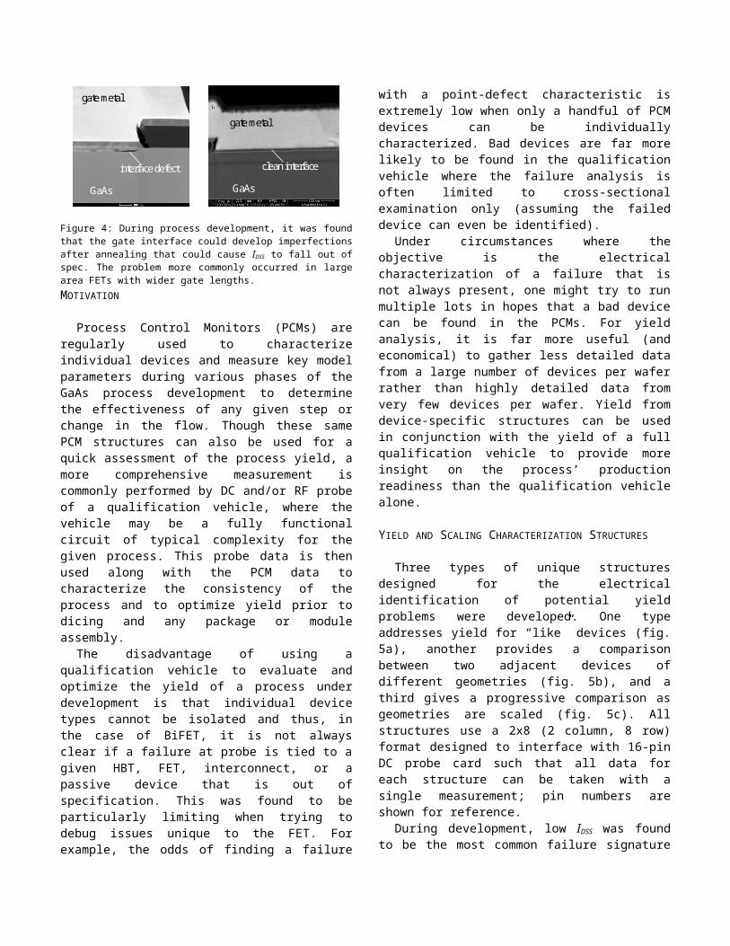
In the earlier stages of BiFET process development, a small percentage of individual devices with abnormally low IDSS were found. Subsequent analysis of the failed devices produced cross-sectional images with visible surface defects in the channel just underneath the gate metal (fig. 4). The

failure was not consistent from lot to lot or from site to site, but problematic enough that our 97% yield target for the new technology release was not being met.
To identify the root cause of the lower FET yield so the issue could be resolved, it was essential to understand the density of these surface defects and have the ability to locate even individual defects over a large surface area. This work focuses on the structures that were developed for the yield analysis and data analysis of those structures.
(a) (b)
(c)
Figure 3: (a) I-V curves of FETs with 1m gate length with backgate connected to source (b) 1m gate length FET with backgate connected to gate (c) statistical data of IDSS vs. Vt for 1m gate length FETs with backgate connected to source, as tracked over 28 completed process runs with 199 wafers and 2531 measured sites.
interface defect
gate metal
GaAs
clean interface
gate metal
GaAs
Figure 4: During process development, it was found that the gate interface could develop imperfections after annealing that could cause IDSS to fall out of spec. The problem more commonly occurred in large area FETs with wider gate lengths.MOTIVATION
Process Control Monitors (PCMs) are regularly used to characterize individual devices and measure key model parameters during various phases of the GaAs process development to determine the effectiveness of any given step or change in the flow. Though these same PCM structures can also be used for a quick assessment of the process yield, a more comprehensive measurement is commonly performed by DC and/or RF probe of a qualification vehicle, where the vehicle may be a fully functional circuit of typical complexity for the given process. This probe data is then used along with the PCM data to characterize the consistency of the process and to optimize yield prior to dicing and any package or module assembly.
The disadvantage of using a qualification vehicle to evaluate and optimize the yield of a process under development is that individual device types cannot be isolated and thus, in the case of BiFET, it is not always clear if a failure at probe is tied to a given HBT, FET, interconnect, or a passive device that is out of specification. This was found to be particularly limiting when trying to debug issues unique to the FET. For example, the odds of finding a failure with a point-defect characteristic is extremely low when only a handful of PCM devices can be individually characterized. Bad devices are far more likely to be found in the qualification vehicle where the failure analysis is often limited to cross-sectional examination only (assuming the failed device can even be identified).
Under circumstances where the objective is the electrical characterization of a failure that is not always present, one might try to run multiple lots in hopes that a bad device can be found in the PCMs. For yield analysis, it is far more useful (and economical) to gather less detailed data from a large number of devices per wafer rather than highly detailed data from very few devices per wafer. Yield from device-specific structures can be used in conjunction with the yield of a full qualification vehicle to provide more insight on the process’ production readiness than the qualification vehicle alone.
YIELD AND SCALING CHARACTERIZATION STRUCTURES
Three types of unique structures designed for the electrical identification of potential yield problems were developed. One type addresses yield for “like” devices (fig. 5a), another provides a comparison between two adjacent devices of different geometries (fig. 5b), and a third gives a progressive comparison as geometries are scaled (fig. 5c). All structures use a 2x8 (2 column, 8 row) format designed to interface with 16-pin DC probe card such that all data for each structure can be taken with a single measurement; pin numbers are shown for reference.
During development, low IDSS was found to be the most common failure signature related to metal-semiconductor interface issues. The most practical way to test for yield would be to lay out a number devices near to each other in
parallel, then measure and compare IDSS for each device individually; but this would be area inefficient. The yield structure of fig. 5a accomplishes the task in a much area efficient manner by using a parallel measurement of many series devices.
(a) (b)
(c)
Figure 5: (a) Yield structure “fetyield_3.4x30_15” featuring 15 identical devices in series over 14 columns. (b) Comparison structure “fetcompare_8” where one device is compared to 8 individual devices connected in series with same net gate length. (c) Scaling structure “fetyield_3.4xL_15” featuring series of like-devices in columns that are progressively compared to series of devices that gradually increase in size.
(a)
(b)
Figure 6: (a) Schematic and (b) Simulation of 15-device FET yield structure “fetyield_3.4x30_15” of Fig. 5a. In the test structure’s layout, IDSS from an individual device at the top of one of the stacks of 15 devices can be taken from the provided I/O. For ADS simulation, a separate device is pulled out so that currents can be compared simultaneously. The ADS simulation shows the individual device starting to break down above 14V.

Figure 7: VDS vs. ID of the 210 device FET yield structure of Fig. 5a. The measurement is repeated across the yield structure’s 14 columns of devices and results overlaid to give an indication of device yield and consistency over the test area. The individual device that can be measured individually in column 1 (at pins 1 and 16) is overlaid for comparison. VDS was set to 1V for the individual device and VDS was set to 15V for each of the 14 column measurements.
Measurement of the structure in fig. 5a will quickly identify any low IDSS failure(s) amongst a set of 210 devices drawn with identical geometries. The test circuit covers a large amount of surface area with active gate layer such that within this area surface defects under the gate metal are readily located. This large area increases the odds of finding a failure. In this case, a failure is defined as an IDSS
measurement that is out of the specification boundaries defined in fig. 3c. In the example shown, the yield of a device with a gate width of 3.4m and a length of 15m is determined for a given location. The same structure was recreated for various size devices so that yield data vs. device size could be gathered.
For a depletion mode device, IDSS can be measured using only two terminals and connecting the device in a current source configuration. In this case, one applies a bias to the drain when the gates and source are grounded; then, the current Id will remain approximately constant as Vds is varied (assuming the device stays within the saturation region on the low end of Vds and out of breakdown on the high end of Vds).
If we connect a number of current sources together in series, as shown in fig. 6a, the device with the lowest IDSS
will dictate the amount of current flowing through the entire column of devices. Thus, with just one measurement, the lowest IDSS of any given stack of devices is found. When multiple columns of like devices are placed in series and parallel sets as in fig. 5a, an IDSS yield measurement is performed over a given active area. The difference between the single device measurement and series device measurement is highlighted in fig. 7. The turn-on knee will be softer when multiple devices are connected in series but once all devices are in saturation, IDSS depends only on the device geometry, not on the number of series devices. Thus,
for a valid measurement, the voltage across the stack of devices must be high enough to ensure that all devices are operating in the saturated mode.
(a)
(b)
Figure 8: (a) Schematic and (b) measurement vs. simulation of the FET comparison structure “fetcompare_8” of fig. 5b. In the measurement shown Vd is swept from 0 to 7V while monitoring Id and is compared to model simulation.

The test circuits shown in fig. 5b and fig. 5c focus on a relative comparison of adjacent devices and on geometric scaling issues. A schematic of “fetcompare_8” of fig. 5b is shown in fig. 8a. In this case, 8 devices with gate width of 3.4m and a length of 1m connected in drain to source in series are compared to a single device gate width of 3.4m and a length of 8m. Again, the devices are connected in the current source configuration but in the case of the 8 devices in the left column, a common gate connection is used rather than the series of current sources used in the left column of the schematic of fig. 6a. If source and drain parasitic resistances are ignored, then the left and right side IDSS measurements should be identical within the boundaries of expected device-to-device mismatch. When the mismatch is out of a given tolerance range acceptable for analog circuit design, a failure is indicated. A certain amount of part-to-part variation is expected, but less so when comparing immediately adjacent devices.
The circuit of fig. 5c (“fetyield_3.4xL_15”) provides an alternate way to search for point failures, matching problems, and scaling problems. A measure of all three potential issues is taken in one reading. In this case, the devices are connected as per the schematic of fig. 6a; multiple current sources connected in series. By including multiple geometries into the same structure, results can be analyzed in a relative fashion such that a failure is indicated when IDSS does not scale progressively from column to column within the tolerance expected for adjacent devices. In addition, each column can have IDSS confirmed to be within the process boundaries defined in fig. 3c. In the example shown, the gate width is held constant at 3.4m and the gate length is increased in each of the columns stepping from left to right. The measurement is again taken with VDS=15V. The leftmost column with the most narrow gate length is expected to have the highest current. RESULTS
Data was compiled on a wafer-to-wafer basis as well as a lot-to-lot basis. A portion of the data taken near the end of the development cycle is shown in Table 1 after all metal-semiconductor surface problems had been resolved. A failure is indicated when either IDSS was out of spec or when matching was outside of our acceptance criteria. It should be noted that most of the failures shown were most likely wafer-edge related.
TABLE IANALYSIS SUMMARY FOR A GIVEN SET OF WAFERS TOWARDS THE END OF
YIELD OPTIMIZATIONStructure Pass Fail Percent pass
fetcompare_8 366 6 98.36%fetcompare_32 93 0 100.00%fetyield_3.4x30_15 366 6 98.36%fetyield_3.4xL_15 360 24 93.33%
CONCLUSIONS
In this work we have developed and demonstrated specialized yield, scaling, and matching structures to quickly identify problems in active FETs as part of our BiFET technology development. With the help of the new structures, metal-semiconductor interface defects were quickly identified allowing the process problem to be isolated and resolved. After the process was optimized, the same structures were used to show that the yield was greatly enhanced by the process improvements and ready for volume production. It is believed that with these circuits and methods, qualification of future technology iterations can be expedited and that ultimately, higher yields will be achievable in volume production.
ACKNOWLEDGEMENTS
The authors would like to thank Xiao-Ping Li of Skyworks Solutions for help with measurements and additionally thank everybody who contributed to the development and wafer processing of our BiFET technology.
REFERENCES
[1] M. Sun, P. Zampardi, J. Li, R. Ramanathan, A.G. Metzger, C. Cismaru, V. Ho, L. Rushing, K. S. Stevens, M. Chaplin, and R. E. Welser, “A High Yield Manufacturable BiFET Epitaxial Profile for High Volume Production”, 2006 International Conference on Compound Semiconductor Manufacturing Technology (MANTECH), session 9.1, April 24-27, 2006, Vancouver, BC, Canada..
[2] A. Metzger, P. Zampardi, R. Ramanathan, and K. Weller, “Drivers and Applications for an InGaP/GaAs Merged HBT_FET (BiFET) Technology”, Presented at IEEE Radio and Wireless Symposium, Jan. 14-20, 2006.
[3] P. Zampardi, C. Cismaru, J. Li, A. Metzger, H. Shen, M. Sun, L. Rushing, R. Ramanathan, J. Yota, S. Machuga, and K. Weller, “High-Volume Manufacturing Considerations for III-V Merged HBT-FET (BiFET Technologies)”, Technical Digest of the 2005 Compound Semiconductor Manufacturing Expo (CS-MAX), pp. 32-34, October/November 2005.
[4] C.E. Chang, Ph.D. thesis, “Novel Low Power HBT Technology”, University of California, San Diego, 1995.
[5] D. Cheskis, C.E. Chang, W.H. Ku, P.M. Asbeck, M.F. Chang, R.L. Pierson, and A. Sailer, “Co-integration of GaAlAs/GaAs HBTs and GaAs FETs with a Simple, Manufacturable Process”, IEEE Electron Devices Meeting, 13-16 Dec. 1992 Page(s): 91 – 9
ACRONYMSHBT: Heterojunction Bipolar TransistorFET: Field Effect Transistor BiFET: Bipolar / Field Effect TransistorPCM: Process Control Monitor
