partitioning and placement for buildable qca circuits · partitioning and placement for buildable...
TRANSCRIPT

Partitioning and Placement for BuildableQCA Circuits
SUNG KYU LIM, RAMPRASAD RAVICHANDRAN, and MIKE NIEMIERGeorgia Institute of Technology
Quantum-dot Cellular Automata (QCA) is a novel computing mechanism that can represent binaryinformation based on spatial distribution of an electron charge configuration in chemical molecules.In this article, we present the first partitioning and placement algorithm for automatic QCA layout.We identify several objectives and constraints that will enhance the buildability of QCA circuits.The results are intended to: (1) define what is computationally interesting and could actually bebuilt within a set of predefined constraints, (2) project what designs will be possible as additionalconstructs become realizable, and (3) provide a vehicle that we can use to compare QCA systemsto silicon-based systems.
Categories and Subject Descriptors: B.7.2 [Design Aid]: Placement and Routing
General Terms: Algorithms, Design
Additional Key Words and Phrases: Nanotechnology, quantum-dot cellular automata, partitioning,placement
1. INTRODUCTION
Nano technology and devices will have revolutionary impact on the computer-aided design (CAD) field. Similarly, CAD research at circuit, logic, and archi-tectural levels for nano devices can provide valuable feedback to nano researchand illuminate ways for developing new nano devices. It is time for CAD re-searchers to play an active role in nano research. One approach to computingat the nano-scale is the quantum-dot cellular automata (QCA) concept thatrepresents information in a binary fashion but replaces a current switch witha cell having a bistable charge configuration. QCA devices can be realized inmetal [Amlani et al. 1998] or with chemical molecules [Lieberman et al. 2002].A wealth of experiments have been conducted with metal-dot QCA, with in-dividual devices [Amlani et al. 1998], logic gates [Snider et al. 1999; Amlani
This research is partially supported by the National Science Foundation under NER-0404011.Authors’ addresses: S. K. Lim, School of Electrical and Computer Engineering, Georgia Instituteof Technology, 777 Atlantic Drive NW, Atlanta, GA 30332-0250; email: [email protected];R. Ravichandran and M. Niemier, College of Computing, Georgia Institute of Technology, Atlanta,GA.Permission to make digital or hard copies of part or all of this work for personal or classroom use isgranted without fee provided that copies are not made or distributed for profit or direct commercialadvantage and that copies show this notice on the first page or initial screen of a display alongwith the full citation. Copyrights for components of this work owned by others than ACM must behonored. Abstracting with credit is permitted. To copy otherwise, to republish, to post on servers,to redistribute to lists, or to use any component of this work in other works requires prior specificpermission and/or a fee. Permissions may be requested from Publications Dept., ACM, Inc., 1515Broadway, New York, NY 10036 USA, fax: +1 (212) 869-0481, or [email protected]© 2005 ACM 1550-4832/05/0400-0050 $5.00
ACM Journal on Emerging Technologies in Computing Systems, Vol. 1, No. 1, April 2005, Pages 50–72.

Partitioning and Placement for Buildable QCA Circuits • 51
et al. 1999], wires [Snider et al. 1999], latches [Kummamuru et al. 2002], andclocked devices [Kummamuru et al. 2002]. These advancements have been fol-lowed by various recent efforts in developing CAD tools for QCA-based circuitsand systems [Gergel et al. 2003; Bernstein 2003; Walus et al. 2004; J. Huang andLombardi 2004]. A recent work on ILP-based QCA circuit partitioning is pre-sented in Antonelli et al. [2004], where the authors partition individual gatesto timing zones so that the difference in clocking zone heights is minimized.
Our goal in this article is to explain how CAD can help research move fromsmall circuits to small systems of quantum-dot cellular automata (QCA) de-vices. We leverage our ties to physical scientists who are working to build realQCA devices. Based upon this interaction, a set of near-term buildability con-straints has evolved—essentially a list of logical constructs that are viewed asimplementable by physical scientists in the near-term. Until recently, most ofthe design optimizations have been done by hand. These initial attempts toautomate the process of removing a single, undesirable, and unimplementablefeature from a design were quite successful. We now intend to use CAD, espe-cially physical layout automation, to address all undesirable features of designthat could hinder movement toward a “buildability point” in QCA. The net re-sult should be an expanded subset of computationally interesting tasks thatcan be accomplished within the constraints of a given buildability point. CADwill also be used to project what is possible as the state-of-the-art in physicalscience expands.
In this article, we present the first partitioning and placement algorithm forautomatic QCA layout. The purpose of zone partitioning is to initially partitiona given circuit such that a single clock potential modulates the interdot barriersin all of the QCA cells within each zone. We then place these zones as well asindividual QCA cells in these zones during our placement step. We identifyseveral objectives and constraints that will enhance the buildability of QCAcircuits and use them in our optimization process. The results are intendedto: (1) define what is computationally interesting and could actually be builtwithin a set of predefined constraints, (2) project what designs will be possibleas additional constructs become realizable, and (3) provide a vehicle that wecan use to compare QCA systems to silicon-based systems.
2. PRELIMINARIES
This section briefly reviews the background of QCA devices and clockingschemes. Then, a detailed comparison between QCA and CMOS technologiesis provided. Lastly, we discuss the need for QCA CAD research, especially thephysical layout automation.
2.1 QCA Circuit Building Blocks
QCA circuits are built from the following components.
2.1.1 QCA Device. A high-level diagram of a “candidate” four-dot metalQCA cell appears in Figure 1(a) [Amlani et al. 1998]. It depicts four quantumdots that are positioned to form a square. Exactly two mobile electrons are
ACM Journal on Emerging Technologies in Computing Systems, Vol. 1, No. 1, April 2005.

52 • S. K. Lim et al.
Fig. 1. Illustration of QCA device, majority gate, and wires.
loaded into this cell and can move to different quantum dots by means of electrontunnelling. Coulombic repulsion will cause classical models of the electrons tooccupy only the corners of the QCA cell, resulting in two specific polarizations.These polarizations are configurations where electrons are as far apart fromone another as possible in an energetically minimal position, without escapingthe confines of the cell.
2.1.2 QCA Logic Gate. QCA’s logic functionality will be explained in termsof generic 4-dot cells. The fundamental QCA logical gate is the three-inputmajority gate. It consists of five cells and implements the logical equationAB+BC+AC as shown in Figure 1(b). Computation is performed by driv-ing the device cell to its lowest energy state which will occur when it as-sumes the polarization of the majority of the three input cells. Here, theelectrostatic repulsion between the electrons in the three input cells andthe electrons in the device cell will be at a minimum. As the majority func-tion can be reduced to the AND and OR function, and a means for sig-nal inversion is possible [Amlani et al. 1999], QCA’s logic set is functionallycomplete.
2.1.3 QCA Wire. One way of moving data from point A to point B in aQCA circuit is with a 90-degree wire. The wire is called “90-degrees” as thecells from which it is made up are oriented at a right angle. The wire is ahorizontal row of QCA cells, and a binary signal propagates from left-to-rightbecause of electrostatic interactions between adjacent cells. A QCA wire can alsobe comprised of cells rotated 45-degrees. Here, as a binary signal propagatesdown the length of the wire, it alternates between a binary 1 and a binary 0polarization. QCA wires possess the unique property that they are able to crossin the plane without the destruction of the value being transmitted on eitherwire as shown in Figure 1(c). This property holds only if the QCA wires are ofdifferent orientations (i.e. a 45-degree wire crossing a 90-degree wire [Snideret al. 1999]). However, it is most important at present that all layout is assumedto be two-dimensional.
2.1.4 QCA Clock. QCA’s clock was first characterized by Lent et al. [2000]as having 4 phases. During the first clock phase (switch), QCA cells begin asunpolarized with low interdot potential barriers. During this phase, barriersare raised, and the QCA cells become polarized according to the state of theirdrivers (i.e. their input cells). It is in this clock phase that actual switching (orcomputation) occurs. By the end of the clock phase, barriers are high enough to
ACM Journal on Emerging Technologies in Computing Systems, Vol. 1, No. 1, April 2005.

Partitioning and Placement for Buildable QCA Circuits • 53
suppress any electron tunnelling and cell states are fixed. During the secondclock phase (hold), barriers are held high so the outputs of the subarray that hasjust switched can be used as inputs to the next stage. In the third clock phase,(release), barriers are lowered and cells are allowed to relax to an unpolarizedstate. Finally, during the fourth clock phase (relax), cell barriers remain lowand cells stay in an unpolarized state [Tougaw and Lent 1994].
Individual QCA cells need not be clocked or timed separately. However, aphysical array of QCA cells can be divided into zones that offer the advantageof multiphase clocking and group pipelining. For each zone, a single potentialwould modulate the interdot barriers in all of the cells in a given zone. Such aclocking scheme allows one zone of QCA cells to perform a certain calculation,have its state frozen by the raising of interdot barriers, and then have the outputof that zone act as the input to a successor zone.
In a molecular implementation of QCA, the four phases of a clock signalwould most likely take the form of time-varying but repetitious voltagesapplied to silicon wires embedded underneath some substrate to which QCAcells were attached. Every fourth wire would receive the same voltage at thesame time [Hennessy and Lent 2001]. Neighboring wires see delayed formsof the same signal. The charge and discharge of the embedded silicon wireswill move the area of activity (i.e. computation or data movement) across themolecular layer of QCA cells with computation occurring at the leading edge ofthe applied electric field. Computation moves across the circuit in a continuous“wave” [Tougaw and Lent 1994].
2.2 QCA Wins
As QCA is being considered as an alternative to silicon-based computation, it isappropriate to enumerate what QCA’s “advantages” over silicon-based systemscould be (as well as its potential obstacles). We begin by listing obstacles toCMOS-based Moore’s Law design (Table I), their effects on silicon-based sys-tems, and how they will affect QCA.
Based on the information in Table I, it is apparent that QCA faces some ofthe same general problems as silicon-based systems (timing issues, lithographyresolutions, and testing), that QCA does not experience some of the problemsof silicon-based systems (quantum effects and tunnelling), and that silicon-based systems can address one problem better than QCA currently can (I/O).However, if the I/O problem is resolved, QCA can potentially offer significant“wins” with regard to reduced power dissipation and fabrication. Additionally,QCA can also offer orders of magnitude in potential density gains when com-pared to silicon-based systems. When examining the existing design of an ALUfor a simple processor [Niemier and Kogge 2001], one version is potentially1800 times more dense (assuming deterministic cell placement) than an end ofthe CMOS curve equivalent (0.022 micron process). If based on a more imple-mentable FPGA (whose logic cell is a single NAND gate), the ALU is no lessdense than a fully custom, end of the CMOS curve equivalent [Niemier andKogge 2004]. Clearly, realizable and potential QCA systems warrant furtherstudy.
ACM Journal on Emerging Technologies in Computing Systems, Vol. 1, No. 1, April 2005.

54 • S. K. Lim et al.
Table I. Comparing Characteristics of Silicon-Based Systems to QCA-Based Systems
Obstacle Effect on CMOS Circuits How it Relates to QCAQuantum
EffectsandTunneling
A gate that controls the flow ofelectrons in a transistor could allowthem to tunnel through smallbarriers—even if the device issupposed to be off [Packan 1999].
No effect; QCA devices are chargecontainers not current switches andactually leverage this property.
High powerdissipation
Chips could melt [Rabaey 1996; Meadand Conway 1980] unless problemsare overcome for which the SIAroadmap says “there are no knownsolutions”. 2014 projection: a chipwith 1010 devices dissipates 186Wof power.
1011 QCA devices with 10−12 switchingtimes dissipate 100W of power.QCA’s silicon-based clock will alsodissipate power. Still, clocking wiresshould move charge adiabatically[Hennessy and Lent 2001], greatlyreducing power consumption.
Slow wires Wires continue to dominate the overalldelay [Ho et al. 2001]. Also,projections show that for 60 nmfeature sizes, less than 10% of thechip is reachable in 1-clock cycle[Hamilton 1999].
The inherent pipelining caused by theclock make global communicationand signal broadcast difficult[Niemier 2003]. Problems aresimilar to silicon-based systems butfor different reasons.
Lithographyresolutions
Shorter wave lengths and largerapertures are needed to provide finerresolutions for decreased featuresizes.
QCA’s clock wiring is donelithographically which is subject tothe same constraints assilicon-based systems. However,closely spaced nano-wires could alsobe used [Lieberman et al. 2002].
Chip I/O I/O count continue to increase as thetechnology advances (Rent’s rule),but pin counts do not scale well.With more processing power, we willneed more I/O [Rabaey 1996].
I/O remains under investigation withone approach to include “stickyends” at the ends of certain DNAtiles in order to bind nano-particlesor nano-wires
Testing Even if designs are verified andsimulated, defects caused byimpurities in the manufacturingprocess, misalignment, brokeninterconnections, etc., can allcontribute to nonfunctional chips.Testing does not scale well [Rabaey1996].
We must find and route around defectscaused by self-assembly and/or findnew design methodologies to makecircuits robust. Defects forself-assembled systems could rangefrom 70% to 95%. Structures such asthicker wires could help.
Cost Fabrication facility cost doublesapproximately every 4.5 years[Rutten 2001], and could reach 200billion dollars in 2015.
Self-assembly could be much moreinexpensive.
2.3 Buildability Analysis via QCA CAD
One might argue that it would be premature to perform any systems-level studyof an emergent device while the physical characteristics of a device continue toevolve. However, it is important to note that many emergent, nano-scale devicesare targeted for computational systems—and to date, most system-level studieshave been proposed by physical scientists and usually end with a demonstra-tion of a functionally-complete logic set or a simple adder. Useful and efficientcomputation will involve much more than this, and, in general, it is important
ACM Journal on Emerging Technologies in Computing Systems, Vol. 1, No. 1, April 2005.

Partitioning and Placement for Buildable QCA Circuits • 55
to provide scientists with a better idea of how their devices should function.This coupling can only lead to an accelerated development of functional and in-teresting systems at the nano-scale. More specifically, with QCA, physicists arecurrently preparing to test the self-assembly process and its building blocks.Thus, our work can help provide the physicists with computationally interest-ing patterns—the real and eventual desired end result.
Our toolset will focus on the following undesirable design schematic charac-teristics associated with a near-to-midterm buildability point: large amountsof deterministic device placement, long wires, clock skew, and wire crossings.We will use CAD to: (1) identify logic gates and blocks that can be duplicatedto reduce wire crossings, (2) rearrange logic gates and nodes to reduce wirecrossings, (3) create shorter routing paths to logical gates (to reduce the risk ofclock skew and susceptibility to defects and errors), and (4) reduce the area of acircuit (making it easier to physically build). Some of these problems have beenindividually considered in existing work for silicon-based VLSI design. Someexamples include clock routing with skew minimization [Tsay 1993], logic du-plication with delay minimization [Enos et al. 1999], placement with wirelengthminimization [Kleinhans et al. 1991], and floorplanning with area minimiza-tion [Murata et al. 1995]. However, wire crossing rarely becomes an issue inCMOS circuits due to the availability of multiple routing layers and vias. At thispoint, QCA routing is restricted to planar, with a very limited number of wirecrossing permitted. Thus, wire crossing minimization is crucial in improvingthe buildability of QCA layouts.
2.4 CMOS vs QCA Placement
Although QCA and CMOS have considerable technological differences, CMOSVLSI placement algorithms [Dunlop and Kernighan 1985; Kernighan et al.1991; Sun and Sechen 1995] have been modified to satisfy the design con-straints imposed by QCA physical science. There are many reasons for usingthis approach. Notably, VLSI design automation algorithms work on graph-based circuits, and it has been found to be advantageous to represent QCAcircuits as graphs especially because, at present, only two-dimensional circuitshave been proposed and are seen as technically feasible. Existing algorithmscan be finetuned to meet QCA’s constraints and objectives. Additionally, phys-ical design issues for CMOS have been widely studied, optimized, and provento be NP-complete [Garey and Johnson 1979]. Thus, it makes sense to leveragethis existing body of knowledge and apply it to a new problem. Finally, becauseso few design automation tools and methodologies exist for QCA, using VLSIalgorithms as a base will allow us to compare and set standards for our placeand route methodologies.
More specifically, we note the following similarities and differences betweenCMOS and QCA placement.
—Similarity. In CMOS placement, in order to efficiently handle the designcomplexity, partitioning, floorplanning, and placement are performed in or-der (hierarchical approach). We use a similar approach in QCA placement:zone partitioning, zone placement, and cell placement. The objectives are
ACM Journal on Emerging Technologies in Computing Systems, Vol. 1, No. 1, April 2005.

56 • S. K. Lim et al.
common in both CMOS and QCA partitioning for the same purpose, namely,cut size and performance. The area, performance, congestion, and wirelengthobjectives are common in both CMOS and QCA placement.
—Difference. Two major sources of the difference between CMOS and QCAare QCA clocking and the QCA single-layer routing resource. Wire crossingminimization is critical in QCA placement since QCA layout needs to be donein a single layer, unlike the multilayer CMOS layout. Thus, node duplicationin CMOS targets area and performance, while QCA duplication focuses onwire crossing. In order to meet the QCA clocking requirement, we use k-layered bipartite graphs to represent the original and partitioned netlist.This, in turn, requires QCA partitioning to minimize area increase (afterthe bipartite graph construction). In addition, the length of all reconvergentpaths from the same partition should be balanced (discussed in detail later)and cyclic dependency is not allowed.
3. PROBLEM FORMULATION
In this section, we provide an overview of the placement process of QCA circuits.We then present the formulation of three problems related to QCA placement—zone partitioning, zone placement, and cell placement problem. Our recent workon zone partitioning and zone placement is available in Nguyen et al. [2003]and our work on cell placement in Ravichandran et al. [2004].
3.1 Overview of the Approach
QCA placement is divided into three steps: zone partitioning, zone placement,and cell placement. The purpose of zone partitioning is to decompose an inputcircuit such that a single potential modulates the inner-dot barriers in all ofthe QCA cells that are grouped within a clocking zone. Unless QCA cells aregrouped into zones to provide zone-level clock signals, each individual QCAcell will need to be clocked. The wiring required to clock each cell individuallywould easily overwhelm the simplicity won by the inherent local connectivityof QCA architecture. However, because the delay of the biggest partition alsodetermines the overall clock period, the size of each partition must also be de-termined carefully. In addition, four-phase clocking imposes a strict constrainton how to perform partitioning. The zone placement step takes as input a setof zones with each zone assigned a clocking label obtained from zone partition-ing. The output of zone placement is the best possible layout for arranging thezones on a two-dimensional chip area. Finally, cell placement visits each zoneto determine the location of each individual logic QCA cell, a cell used to buildmajority gates. An illustration of the QCA placement and routing step is shownin Figure 2.
3.2 Zone Partitioning Problem
A gate-level circuit is represented with a directed acyclic graph (DAG) G(V , E).Let P denote a partitioning of V into K nonoverlapping and nonempty blocks.Let G ′(V ′, E ′) be a graph derived from P , where V ′ is a set of logic blocks, andE ′ is a set of cut edges based on P . A directed edge e(x, y) is cut if x and y
ACM Journal on Emerging Technologies in Computing Systems, Vol. 1, No. 1, April 2005.

Partitioning and Placement for Buildable QCA Circuits • 57
Fig. 2. Overview of the QCA layout automation process. A logic and a wire block are shown. First,the input circuit is partitioned into logic and wire blocks (zone partitioning). Second, each blockis placed onto 2D-space while satisfying QCA timing constraints (zone placement). Third, QCAcells in each block is placed (QCA cell placement). Fourth, routing is performed to finish interblockinterconnect (global QCA routing) and intrablock interconnect (detailed QCA routing).
Fig. 3. Illustration of reconvergent path constraint: (a) All three reconvergent paths from S to Tare unbalanced. If S is in the switch phase, A, B, and T will be in relax, release, and hold phase.This puts C and T into relax and release, thereby causing a conflict at T . The bottom path forces Tto be in switch phase, causing more conflict. (b) Wire blocks W1, W2, and W3 are inserted to resolvethis QCA clocking inconsistency. (c) Some wire blocks are shared to minimize the area overhead.
belong to different blocks in P . Two paths p and q in G ′ are reconvergent if theydiverge from and reconverge to the same blocks as illustrated in Figure 3(a). Ifl (p)denotes the length of a reconvergent path p in G ′ then l (p) is defined to bethe number of cut edges along p. A formal definition of the zone partitioningproblem is as follows.
Definition 3.1. In zone partitioning, we seek a partitioning of logic gatesin the given netlist into a set of zones so that cutsize (= total number of cutnets) and wire block (= required during the subsequent zone placement) areminimized. The area of each partition needs to be bounded (area constraint),and cyclic dependency among partitions (acyclic constraint) should not exist.In addition, the length of all reconvergent paths should be balanced (clockingconstraint).
An illustration of reconvergent path constraint is shown in Figure 3. Cyclesmay exist among partitions as long as their lengths are in multiples of four dueto QCA clocking. However, it is hard to enforce this constraint while handlingother objectives and constraints. Therefore, we decide to prevent any cycles
ACM Journal on Emerging Technologies in Computing Systems, Vol. 1, No. 1, April 2005.

58 • S. K. Lim et al.
from forming at the partition level. In addition, it is difficult to maintain thereconvergent path constraint during the partitioning process. Therefore, weallow the reconvergent path constraint to be violated and perform a postprocessto add wire blocks to fix this problem. Since the addition of wire blocks causes theoverall area to increase, we minimize the amount of wire blocks that are neededto completely remove the reconvergent path problems during zone partitioning.
3.3 Zone Placement Problem
Assuming that all partitions (= zone) have the same area, placement of zonesbecomes a geometric embedding of the partitioned network onto a m × n grid,where each logic/wire block is assigned to a unique location in the grid. In thiscase, a bipartite graph exists for every pair of neighboring clocking levels. Wedefine the k-layered bipartite graph as follows.
Definition 3.2. A k-layered bipartite graph is a directed graph G(V , E) ifand only if (i) V is divided into k disjoint partitions, (ii) each partition p isassigned a level, denoted lev(p), and (iii) for every edge e = (x, y), lev( y) =lev(x) + 1.
Therefore, the zone placement problem is to embed a zone-level k-layeredbipartite graph onto an m × n grid so that all blocks in the same layer areplaced in the same row. All the I/O terminals are assumed to be located on thetop and bottom boundary of each block, and we may insert routing channelsbetween clocking levels for the subsequent routing. A formal definition of zoneplacement problem is as follows.
Definition 3.3. For zone placement, we seek to place the zones we obtainfrom zone partitioning onto a 2D space so that area, wire crossings, and wirelength are minimized. Each zone (= logic/wire block) is labeled with a clockinglevel (= longest path length from input zones), and all zones with the sameclocking level should be placed in the same row (clocking constraint). In ad-dition, all interzone wires need to connect two neighboring rows (neighboringconstraint).
3.4 Cell Placement Problem
The input to the cell placement is the zone placement result where all logic/wireblocks at the same clocking level are placed in the same row. Then the outputof cell placement is an arrangement of QCA cells in each logic block. The re-convergent path problem does not exist in cell placement—it is perfectly fineto have unbalanced reconvergent path lengths among the logic gates in eachlogic block. The reason is that correct output values will eventually be avail-able at the output terminals in each block if the clock period is longer than themaximum path delay in each block. We determine the clock period based on themaximum path delay among all logic/wire blocks.
Definition 3.4. In cell placement, we seek a placement of individual logicgates in the logic block so that area, wire crossing, and wirelength areminimized. The following set of constraints exists during QCA cell placement:
ACM Journal on Emerging Technologies in Computing Systems, Vol. 1, No. 1, April 2005.

Partitioning and Placement for Buildable QCA Circuits • 59
(1) the timing constraint—the signal propagation delay from the beginning ofa zone to the end of a zone should be less than a clock period established fromzone partitioning1 and the constraints of physical science (maximum zone de-lay) (i.e., we want to eliminate possible skew), (2) the terminal constraint—theI/O terminals are located on the top and bottom boundaries of each logic block,(3) the signal direction constraint—the signal flow among the logic QCA cellsneeds to be unidirectional, from the input to the output boundary for each zone.
The signal direction is caused by QCA’s clocking scheme where an electricfield E, created by the underlying CMOS wire, is propagating unidirectionallywithin each block. Thus, cell placement needs to be done in such a way as topropagate the logic outputs in the same direction as E. In order to balance thelength of intrazone wires, we construct a cell-level k-layered bipartite graph foreach zone and place this graph.
4. ZONE PARTITIONING ALGORITHM
This section presents our zone partitioning and wire block insertion algorithms.Our zone partitioning algorithm is an iterative improvement-based method,whereas our wire block insertion is based on the longest path computation.
4.1 Zone Partitioning
Let lev(p) denote the longest path length from the input partitions (partitionswith no incoming edges) to partition p, where the path length is the numberof partitions along the path. Then wire(e) denotes the total number of wireblocks to be inserted on an interpartition edge e to resolve the unbalancedreconvergent path problem (clocking constraint of the QCA zone partitioningproblem). Simply, wire(e) = lev( y) + lev(x) − 1 for e = (x, y), and the totalnumber of wiring blocks required without resource sharing is
∑wire(e). Thus,
our heuristic approach is to minimize the∑
wire(e) among all interzone edgeswhile maintaining acyclicity. Then, during postprocessing, any remaining clock-ing problems are fixed by inserting and sharing wire blocks. An illustration ofzone partitioning and wire block insertion is shown in Figure 4.
First, the cells are topologically sorted and evenly divided into a numberof partitions (p1, p2, . . . pk). The partitions are then level-numbered using abreadth-first search. Next, the acyclic FM partitioning algorithm [Cong andLim 2000] is performed on adjacent partitions pi and pi+1. Constraints thatmust be met during any cell move include area and acyclicity. The cell gain hastwo components: cutsize gain and wire block gain. The former indicates thereduction in the number of interpartition wires, whereas the latter indicatesthe reduction in the total number of wire blocks required. We then find the bestpartition based on a combined cost function for both cutsize and wire block gain.Multiple passes are performed on two partitions pi and pi+1 until there is nomore improvement on the cost. Then, this acyclic bipartitioning is performedon partitions pi+1 and pi+2, and so on.
1The longest path delay among all zones determines how fast we can change the global clock fromswitch to hold to release to relax state, that is, the clock rate.
ACM Journal on Emerging Technologies in Computing Systems, Vol. 1, No. 1, April 2005.

60 • S. K. Lim et al.
Fig. 4. Illustration of zone partitioning and wire block insertion: (a) directed graph model of aninput circuit, (b) zone partitioning under acyclicity and reconvergent path constraint, (c) wire blockinsertion where the numbers denote the longest path length. The dotted nodes indicate wire blocks.
Fig. 5. Illustration of clocking level update.
Movement of a single cell can possibly change lev(p), the level number of apartition p. Therefore, every time a cell move is made, we check to see if thiscell move affects the level number. There are two ways levels can change: aninterzone edge is newly introduced or completely removed. In Figure 5, cell a inFigure 5(a) is moved from partition A to B, thereby creating a new interparti-tion edge in 5(b). This, in turn, changes the level of all downstream partitions.In Figure 5(c), cell a in Figure 5(a) is moved from partition A to C, therebyremoving the interpartition edge between A and C 5(c).2 This again changesthe level of all downstream partitions. For updating the level, we maintain amaxparent for each p so that the level number of the parent of p is lev(p) − 1.lev(F ) is defined as the level number of the “from block” of a cell c, and lev(T )is defined as the level number of the “to block” of c. In the first case where anew interpartition edge is created, lev(T ) is updated if lev(F ) ≥ lev(T ) afterthe cell move. In this case, lev(T ) = lev(F ) + 1. Then, we recursively updatethe maxparent and levels of all downstream partitions. The maxparent forpartition C was changed from A to B in Figure 5(b), and lev(C) now becomeslev(B) + 1 = 2. This, in turn, requires the level number of all downstream nodesto change. In the second case, where an existing interpartition edge is removed,
2We assume that a is not the only cell in partition A. This is why the interpartition edge (A, C) stillexists after a moves to partition B.
ACM Journal on Emerging Technologies in Computing Systems, Vol. 1, No. 1, April 2005.

Partitioning and Placement for Buildable QCA Circuits • 61
the maxparent again needs to be updated. The maxparent for partition C waschanged from A to none in Figure 5(c), and lev(C) now becomes lev(C) = 0.
4.2 Wire Block Insertion
During the postprocessing, we fix any remaining clocking problems by insert-ing and sharing wire blocks, while satisfying wire capacity constraints. Theinput to this algorithm is the set of partitions and interpartition edges. First,a super-source node is inserted in the graph whose fan-out neighbors are theoriginal sources in the graph. This is done to ensure that all sources are in thesame clocking zone. Then the single-source longest path is computed for thegraph with the super-source node as the source, and every partition is assigneda clocking level based on its position in the longest path from the source. For agraph with E ′ interpartition edges, this algorithm runs in exactly O(E ′) iter-ations. In the algorithm’s next stage, any edge connecting partitions that areseparated by more than one clock phase is marked, and the edge is added to anarray of bins at every index where a clocking level is missing in the edge. Thefollowing algorithms perform wire block insertion.
wire_block_insertion}(G(V,E))lev(SUPER) = -1;Q.enque(SUPER);BFS-mark(G,SUPER);while (E not empty)
N = E.pop();S = lev(N.source);T = lev(N.sink);while (S + 1 < T$
S = S + 1;BIN[S] = (BIN[S],E);
BFS-mark(G,Q)N = Q.deque;S = set of fanout neighbors of N;while (S is not empty)
A = S.pop();if (LAST-PARENT(A) = N)
lev(A) = lev(N)+1$;Q.enque(A);
BFS-mark(G,Q);
The number of wire blocks in each bin is calculated based on a predeterminedcapacity for the wire blocks. This capacity is calculated based on the width ofeach cell in the grid. Then the interpartition edges are distributed among thewire blocks, filling one wire block to full capacity before filling the next. Itmight seem that a better solution would be to evenly distribute the edges to allthe wire blocks in the current level. This is not true because the wire blockswith the most number of feed-throughs are placed closer to the logical blocks
ACM Journal on Emerging Technologies in Computing Systems, Vol. 1, No. 1, April 2005.

62 • S. K. Lim et al.
Fig. 6. Illustration of zone placement and wire crossing minimization: (a) zone partitioning withwire block insertion, (b) zone placement, where a zone-level k-layered bipartite graph is embeddedonto a 2D space, (c) wire crossing minimization via block re-ordering.
in the next stage. This minimizes wirelength, and hence the number of wirecrossings.
5. ZONE PLACEMENT ALGORITHM
This section presents our zone placement algorithm. Our zone partitioning al-gorithm is an iterative improvement-based method, where the initial placementof a zone-level k-level-bipartite-graph is refined via block swap for wire crossingand wirelength reduction.
5.1 Placement of a K-Layered Bipartite Graph
The logical blocks (obtained from the partitioning stage) and the wire blocks(obtained from postprocessing) are placed on an m × n grid with a given aspectratio and skew. The individual zone dimensions and the column widths are keptconstant to ensure scalability and manufacturability of this design because oth-erwise clocking lines would have to be laid underneath the QCA circuits withgreat precision. The partitions are laid out on the grid with the cells belongingto the first clocking zone occupying the left-most cells of the first row of the grid,and the next level occupying the left-most cell of the next row, and so on, untilrow r. The next level of cells is placed again on row r to the right of the right-most placed cell among the r placed rows. The next level of cells is placed in rowr − 1, and the rest of the cells are placed in a similar fashion until the first rowis reached. This process is repeated until all cells are placed (thereby forminga snake-shape). The white nodes are white space that is introduced becauseof variations in the number of wire and logic blocks among the various clock-ing levels. The maximum wirelength between any two partitions in the griddetermines the clock frequency for the entire grid as all partitions are clockedseparately. For the first and last rows (where interpartition edges are betweenpartitions in two different columns), maximum wirelength was given more pri-ority as maximum wire length at these end zones can be twice as bad as themaximum wire length between partitions on the same column. An illustrationof zone placement and wire crossing minimization is shown in Figure 6.
ACM Journal on Emerging Technologies in Computing Systems, Vol. 1, No. 1, April 2005.

Partitioning and Placement for Buildable QCA Circuits • 63
5.2 Wire Crossing Minimization
During the next phase, blocks are reordered within each clocking level to min-imize interpartition wirelength and wire crossings. Two classes of solutionswere applied to minimize the these objectives: an analytical solution that uses aweighted barycenter method, and Simulated Annealing. The analytical methodonly considers wire crossings since there is a strong correlation between wire-length and number of wire crossings.
Analytical Solution. A widely used method for minimizing wire crossings(introduced by Sugiyama et al. [1981]) is to map the graph into a k-layer bi-partite graph. The vertices within a layer are then permuted to minimize wirecrossings. This method maps well to the problem as we need to only considerthe latter part of the problem (the clocking constraint yields us the k-layerbipartite graph). Still, even in a two-layer graph, minimizing wire crossings isNP-hard [Sugiyama et al. 1981]. Among many heuristics proposed, the barycen-ter heuristic [Sugiyama et al. 1981] has been found to be the best heuristic, ingeneral, for this class of problems. A modified version of the barycenter heuris-tic was used to accommodate for edge weights. The edge weights represent thenumber of interpartition edges that exist between the same pair of partitions.The heuristic can be summarized as follows:
barycenter(v) =∑
N [weight(n) × position(n)]∑
N weight(n),
where v is the vertex in the variable layer, n is the neighbor in the fixed layer,and N is the set of all neighbors in the fixed layer.
Simulated Annealing. A move is done by randomly choosing a level in thegraph and then swapping two randomly chosen partitions [p1, p2] in that levelin order to minimize the total wirelength and wire crossing. In our implemen-tation, the initial calculation of the wirelength takes O(n) and updating wirecrossing takes O(n3), where n is the number of nodes in a layer of the bipartitegraph. In our approach, we initially compute the wirelength and wire crossingand incrementally update these values after each move so that the update canbe done in O(m) time, where m is the number of neighbors for pi. This speed-upallows us to explore a greater number of candidate solutions and, as a result,obtain better quality solutions.
6. CELL PLACEMENT ALGORITHM
This section presents our cell placement algorithm which consists of feed-through insertion, row folding, and wire crossing and wirelength optimizationsteps. Figure 7 shows an illustration of cell placement as well as QCA routing.
6.1 Feed-Through Insertion
In order to satisfy the relative ordering and to satisfy the signal direction con-straint, the original graph G(V , E) is mapped into a k-layered bipartite graphG ′(V ′, E ′) which is obtained by insertion of feed-through gates, where V ′ is theunion of the original vertex set V and the set of feed-through gates, and E ′
is the corresponding edge set. The following algorithm performs feed-throughinsertion.
ACM Journal on Emerging Technologies in Computing Systems, Vol. 1, No. 1, April 2005.

64 • S. K. Lim et al.
Fig. 7. Illustration of cell placement, global routing, and detailed routing: (a) zone placementresult, (b) cell placement result where cells in each partition (= zone) again form a k-layeredbipartite-graph, (c) global routing, where interzone connections are made, (d) detailed routing,where intrazone connections are made.
feed-through_insertion(G(V,E))if (V is empty)
return;n = V.pop();if (n has no child with bigger level)
return;g = new feed-through;lev(g) = lev(n) + 1;for (each child c of n)
c.parent = g;g.child = c;
g.parent = n;n.child = g;add g into G;feed-through_insertion(G(V,E));
In this algorithm, we traverse through every vertex in the vertex set of thegraph. For a given vertex, if any of the outgoing edges terminate at a vertexwith topological order more than one level apart, a new feed-through vertex isadded to the vertex set. The parent of the feed-through is set to the currentvertex, and all children of the current vertex which have a topological orderdifference of more than one is set as the children of the feed-through. We donot need to specifically worry about the exact level difference between the feed-through and the child nodes since this feed-through insertion is a recursiveprocess. This algorithm runs in O(k|V ′|), where k is the maximum degree ofV ′. Figure 8 shows the graph before and after feed-through insertion. A trivialresult of this stage is that all short paths have a set of feed-throughs betweenthe last logical gate in the path and last row.
6.2 Row-Folding Algorithm
After the feed-through insertion stage, some rows may have more gates thanthe average number of gates per row. The row with the largest number of gatesdefines the width of the entire zone, and hence the width of the global column towhich the zone belongs. This increases the circuit area by a huge factor. Hence,
ACM Journal on Emerging Technologies in Computing Systems, Vol. 1, No. 1, April 2005.

Partitioning and Placement for Buildable QCA Circuits • 65
Fig. 8. Illustration of feed-through insertion where a cell-level k-layered bipartite-graph is formedvia feed-through nodes.
rows with a large number of cells are folded into two or more rows. This is doneby inserting feed-through gates in place of the logic gates and moving the gatesto the next row. Row-folding decreases the width of the row since feed-throughshave a lower width than the gate it replaces. A gate g is moved into the nextexisting row if it belongs to the row that needs to be folded, and all paths thatg belongs to contain at least one feed-through with a higher topological orderthan g . The reason for the feed-through condition is that g , along with all gatesbetween g and the feed-through, can be pushed to a higher row, and the feed-through can be deleted without violating the topological ordering constraint.The following algorithm performs row-folding.
row_folding(G,w)if (w is a feed-through)
return(TRUE);if (w.level = G.max_level)
return(FALSE);RETVAL = TRUE;k = w.out-degree;i = 0;while (RETVAL and i<k)
RETVAL = row_folding(G,w.CHILD(i));i = i + 1;
return(RETVAL);
This algorithm returns true if a node can be moved and false if a new row hasto be inserted. If this feed-through criterion is not met, and the row containingg has to be folded, then a new row is inserted and g is moved into that row.
The number of gates that need to be moved from a row that needs foldinginto a new row is given by the following trivial calculation. Let n be the numberof gates that need to be moved to the next row. Let m be the original number ofgates in the row, and let M be the maximum number of gates allowed in a row.Further, let a be the ratio of the width of a feed-through to the width of the gate.Since the width of a gate is always greater than the width of a feed-through,a < 1. For every gate that is moved to a new row, a feed-through has to beinserted in its original place. Hence, after moving n gates to the next row, thewidth of the original row will now be m − n + an, so n = (m − M )/(1 − a). Thiscalculation is repeated for the next row if n is itself greater than the constraint
ACM Journal on Emerging Technologies in Computing Systems, Vol. 1, No. 1, April 2005.

66 • S. K. Lim et al.
M . Our strategy is to fix the width of all zones in each “zone column” andlet the height of each zone grow from row-folding. Our related experimentsindicate that the degree of height increase is well balanced among the zonecolumns which enables us to maintain the initial aspect ratio given by the zoneplacement.
6.3 Wirelength and Wire Crossing Minimization
During the zone placement stage, a zone-level k-layered bipartite graph isformed via wire block insertion. This graph is then placed in such a way thatall zones at the same clocking level are placed in the same row. The samegraph transformation and placement is done during cell placement—a cell-levelk-layered bipartite graph is formed via feed-through insertion, and this graph isplaced in such a way that all cells of the same longest path length are placed inthe same row. In both cases, iterative improvement is performed to reduce thewire crossing and wirelength at the zone and cell level. We perform a barycenterheuristic to build the initial solution and perform block/cell swaps to improvethe solution quality.
To compute the net wirelength in a circuit, we traverse through every vertexand accumulate the difference between the column numbers of the vertex andall of its children. This runs in O(N ), where N is the number of vertices. But,during the first calculation, we store the sum of all outgoing wirelength inevery vertex. This enables us to incrementally update if the position of only onenode changes. A node cannot change its row number since, at this stage, thetopological level is fixed. If a node changes its position within a level, then itis enough to calculate the difference in position with respect to its neighborsalone. Hence, the subsequent wirelength calculation is reduced to O(K ) whereK is the node’s vertex degree.
Wire-crossing computation can be done with either the adjacency list or ma-trix, depending on the sparseness of the graph. We used the adjacency matrixto compute the number of wire crossings in a graph. In a graph, there is a wirecrossing between two layers v and u if vi talks to u j , and vx talks to uy , wherei, j , x, and y denote the relative positional ordering in the nodes, and either,i < x < j < y or i < x < y < j or x < i < y < j or x < i < j < y , without lossof generality. In terms of an adjacency matrix, this can be regarded as if eitherthe point (i, j ) is in the lower left submatrix of (x, y) or vice versa, there is acrosstalk. Hence, our solution is to count the number of such occurrences. If thiscounting is done unintelligently, it can be in the order of O(n4). Our algorithmto compute the number of wire crossings runs in O(n2).
Figure 9 shows an example of wire-crossing computation. The graph inFigure 9(a) can be represented by the adjacency matrix shown in Figure 9(b).The number of crossings in Figure 9(a) is 3. This can be obtained from thematrix by adding the product of every matrix element and the sum of its left-lower matrix elements. That is, the number of crossings is
∑(Aij × ∑ ∑
Axy),where i + 1 < x < n and 1 < y < j − 1. This formula gives a good intuitionof the process but is computationally very expensive. We now illustrate ourmethod to calculate wire crossing more efficiently. First, we take the row-wise
ACM Journal on Emerging Technologies in Computing Systems, Vol. 1, No. 1, April 2005.

Partitioning and Placement for Buildable QCA Circuits • 67
Fig. 9. Illustration of an incremental wire-crossing computation: (a) a bipartite graph with 3 wirecrossings, (b) adjacency matrix of (a), (c) row-wise sum of (b) from left to right, (d) column-wise sumof (c) from bottom to top. Each entry in (d) now represents the total sum of entries in lower-leftsubmatrix. Using (b) and (d), wire crossing is A2 × B1 + B3 × C2 = 3, where A2 and B3 are from(b) and B1 and C2 from (d).
sum of all entries as shown in Figure 9(c). Then we use this to compute thecolumn-wise sum as in 9(d). Finally, we multiply all the entries in the originalmatrix and the column-wise sum matrix to compute the total wire crossing—each entry (r, c) in the original matrix is multiplied by the entry (r + 1, c − 1)in the column-wise sum matrix as shown in 9(d). In the simulated annealingprocess, when we swap two nodes, it is identical to swapping the correspondingrows in the above matrices. Hence, it is enough if we just update the values ofthe rows in between the two rows that are being swapped. The pseudocode forthis incremental algorithm is as follows.
calc_wire_crossing(R_1, R_2, M)if (R_2<R_1)
return(calc\_wire\_crossing(R_2,R_1,M));sum = pos = neg = diff = j = 0;while (j < NumRows)
tmp = diff;i = R_2-1;while (i > R1)
sum = sum + M[i][j]*(pos-neg);diff = diff + M[i][j];i = i + 1;
sum = sum - M[R_1][j]*(tmp+neg);sum = sum + M[R_2][j]*(tmp+pos);pos = pos + M[i][j];neg = neg + M[R_2][j];
return(sum);
During cell placement, a move is done by randomly choosing a level in thegraph and then swapping two randomly chosen gates [g1, g2] in that level in or-der to minimize the total wirelength and wire crossing. In our implementation,the initial calculation of the wire length takes O(n) and updating wire crossingtakes O(n2), where n is the number of nodes in a layer of the bipartite graph.In our approach, we initially compute the wirelength and wire crossing andincrementally update these values after each move so that the update can bedone much faster as illustrated. This speed-up allows us to explore a greater
ACM Journal on Emerging Technologies in Computing Systems, Vol. 1, No. 1, April 2005.

68 • S. K. Lim et al.
Table II. QCA Zone Partitioning Results
Acyclic FM Zone PartitionerName Cut White Wire Cut White Wire
b14 2948 151 138 2566 168 127b15 4839 220 260 4119 144 256b17 16092 1565 1789 13869 1616 1710b20 6590 641 519 6033 642 518b21 6672 599 560 6141 622 557b22 9473 1146 1097 8518 1158 1098s13207 2708 143 138 1541 144 137s15850 3023 257 183 2029 254 181s35932 7371 875 1014 5361 734 1035s38417 9375 757 784 5868 775 773s38584 9940 1319 1155 7139 1307 1095s5378 1206 34 30 866 34 30s9234 1903 99 81 1419 104 76
Ave 6318 600 596 5036 592 584Ratio 1 1 1 0.8 0.99 0.98time 14646 14509
number of candidate solutions, and as a result, obtain better quality solutions.We set the initial temperature such that roughly 50% of the bad moves wereaccepted. The final temperature was chosen such that less than 5% of the moveswere accepted. We used three different cost functions. The first cost functiononly optimized based on the net wirelength. The second cost function evaluatedthe number of wire crossings, while the last cost function looked at a weightedcombination of both. The weights used were the ratio between the wirelengthand the number of wire crossings obtained in the analytical solution.
7. EXPERIMENTAL RESULTS
Our algorithms were implemented in C++/STL, compiled with gcc v2.96, runon a Pentium III 746MHz machine. The benchmark set consists of the sevenbiggest circuits from ISCAS89 and the five biggest circuits from ITC99 suitesdue to the availability of signal flow information.3
7.1 Zone Partitioning Results
Table II shows the zone partition results for our QCA placement. The numberof partitions is determined such that there are 100 ± 10 majority gates perpartition. We set the capacity of each wire block to 200 QCA cells. We compareacyclic FM [Cong and Lim 2000] and QCA zone partitioning in terms of cutsize,white space, and wire blocks needed after zone placement. With a QCA partition,we see a 20% improvement in cutsize at the cost of a 6% increase in run-time.A new algorithm was implemented to reduce the number of white spaces, by
3Several points prevent us from comparing our results to another recent QCA partitioning work,Antonelli et al. [2004]. First, the design objective is different—we focus more on wire crossingand skew minimization while Antonelli et al. [2004] focuses on area skew. Second, the authorsused randomly generated small-size circuits, whereas we use a standard set of benchmarks withmedium- to large-scale.
ACM Journal on Emerging Technologies in Computing Systems, Vol. 1, No. 1, April 2005.

Partitioning and Placement for Buildable QCA Circuits • 69
Table III. QCA Zone Placement Results
Analytical SA-BasedName Area Length Xing Length Xing
b14 20 × 17 81 67 23 67b15 20 × 24 59 90 34 90b17 69 × 52 3014 346 305 345b20 36 × 36 414 165 99 166b21 36 × 37 140 172 100 172b22 48 × 50 1091 230 188 230s13207 18 × 21 28 9 28 9s15850 24 × 23 81 16 11 14s35932 45 × 44 1313 64 78 68s38417 42 × 43 493 54 48 54s38584 55 × 48 1500 102 110 80s5378 10 × 10 3 10 2 9s9234 15 × 16 15 11 5 11
Ave 633 103 79 101Ratio 1 1 0.13 0.98time 23 661
taking into account terminal propagation [Dunlop and Kernighan 1985]. Ournew algorithm for reducing the number of white nodes involves moving wireblocks to balance the variation in the number of partitions per clocking level.Although our algorithm results in a 67% decrease in wire nodes and 66% de-crease in white nodes, there is a tradeoff in a resulting increase in the numberof wire crossings. Since wire crossings have been seen as a much more signif-icant problem, we choose to sacrifice an increase in area for a decrease in thenumber of wire crossings.
7.2 Zone Placement Results
Table III details our zone placement results where we report placement area,wirelength, and wire crossings for the benchmark circuits. We compare theanalytical solution to simulated annealing. Comparing simulated annealingto the analytical solution, we see an 87% decrease in wirelength and a slightincrease in wire crossings.
7.3 Cell Placement Results
Table IV shows our cell placement results where we report net wirelength andnumber of wire crossings for the circuits using our analytical solution and allthree flavors of our simulated annealing algorithm. We further tried simulatedannealing from an analytical start, and the results were identical to the an-alytical solution. We observe in general that the analytical solution is betterthan all three flavors of the Simulated Annealing methods except in terms ofwirelength in the case of the weighted Simulated Annealing process. But, thetradeoff in wire crossings makes the analytical solution more viable since wirecrossings pose a bigger barrier than wirelength in QCA architecture.
One interesting note is that, when comparing among the three flavors ofsimulated annealing, we find that simulated annealing with wire-crossing
ACM Journal on Emerging Technologies in Computing Systems, Vol. 1, No. 1, April 2005.
70 • S. K. Lim et al.
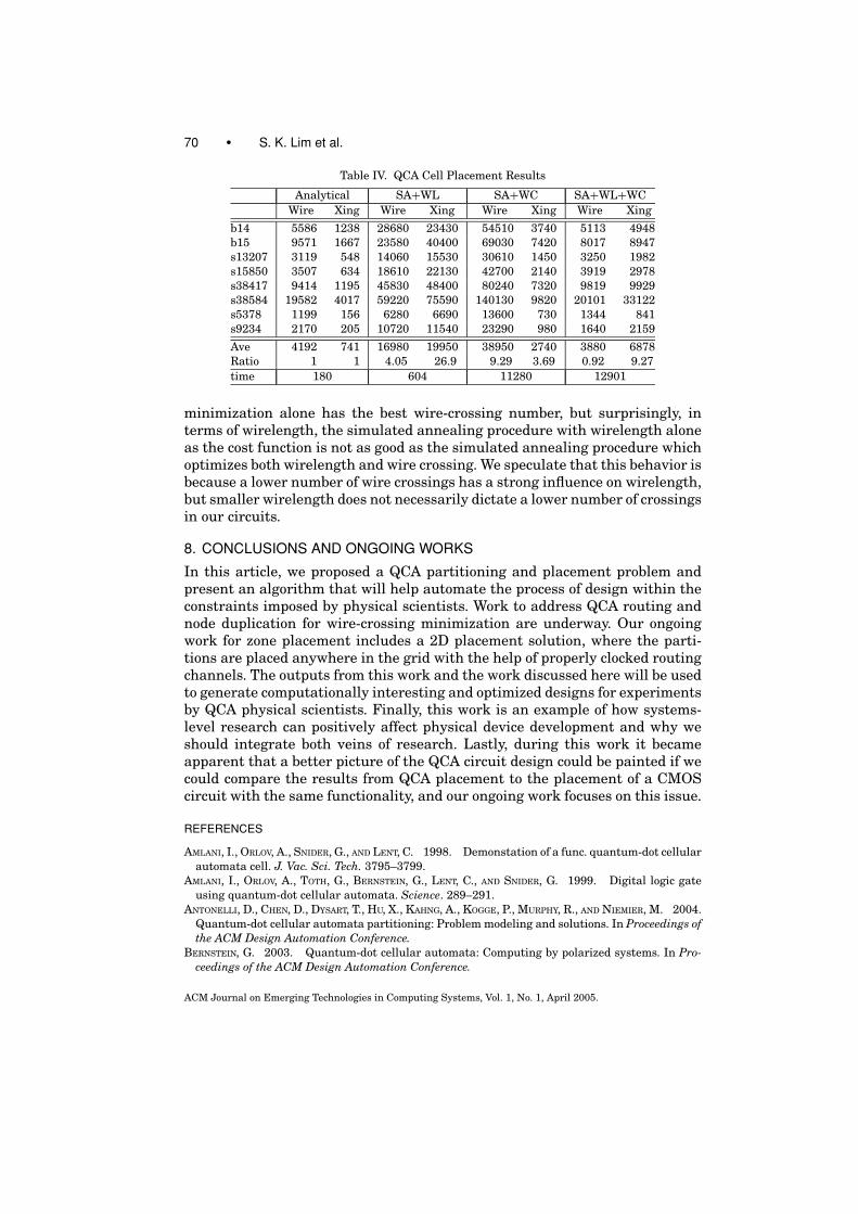
Table IV. QCA Cell Placement Results
Analytical SA+WL SA+WC SA+WL+WCWire Xing Wire Xing Wire Xing Wire Xing
b14 5586 1238 28680 23430 54510 3740 5113 4948b15 9571 1667 23580 40400 69030 7420 8017 8947s13207 3119 548 14060 15530 30610 1450 3250 1982s15850 3507 634 18610 22130 42700 2140 3919 2978s38417 9414 1195 45830 48400 80240 7320 9819 9929s38584 19582 4017 59220 75590 140130 9820 20101 33122s5378 1199 156 6280 6690 13600 730 1344 841s9234 2170 205 10720 11540 23290 980 1640 2159
Ave 4192 741 16980 19950 38950 2740 3880 6878Ratio 1 1 4.05 26.9 9.29 3.69 0.92 9.27time 180 604 11280 12901
minimization alone has the best wire-crossing number, but surprisingly, interms of wirelength, the simulated annealing procedure with wirelength aloneas the cost function is not as good as the simulated annealing procedure whichoptimizes both wirelength and wire crossing. We speculate that this behavior isbecause a lower number of wire crossings has a strong influence on wirelength,but smaller wirelength does not necessarily dictate a lower number of crossingsin our circuits.
8. CONCLUSIONS AND ONGOING WORKS
In this article, we proposed a QCA partitioning and placement problem andpresent an algorithm that will help automate the process of design within theconstraints imposed by physical scientists. Work to address QCA routing andnode duplication for wire-crossing minimization are underway. Our ongoingwork for zone placement includes a 2D placement solution, where the parti-tions are placed anywhere in the grid with the help of properly clocked routingchannels. The outputs from this work and the work discussed here will be usedto generate computationally interesting and optimized designs for experimentsby QCA physical scientists. Finally, this work is an example of how systems-level research can positively affect physical device development and why weshould integrate both veins of research. Lastly, during this work it becameapparent that a better picture of the QCA circuit design could be painted if wecould compare the results from QCA placement to the placement of a CMOScircuit with the same functionality, and our ongoing work focuses on this issue.
REFERENCES
AMLANI, I., ORLOV, A., SNIDER, G., AND LENT, C. 1998. Demonstation of a func. quantum-dot cellularautomata cell. J. Vac. Sci. Tech. 3795–3799.
AMLANI, I., ORLOV, A., TOTH, G., BERNSTEIN, G., LENT, C., AND SNIDER, G. 1999. Digital logic gateusing quantum-dot cellular automata. Science. 289–291.
ANTONELLI, D., CHEN, D., DYSART, T., HU, X., KAHNG, A., KOGGE, P., MURPHY, R., AND NIEMIER, M. 2004.Quantum-dot cellular automata partitioning: Problem modeling and solutions. In Proceedings ofthe ACM Design Automation Conference.
BERNSTEIN, G. 2003. Quantum-dot cellular automata: Computing by polarized systems. In Pro-ceedings of the ACM Design Automation Conference.
ACM Journal on Emerging Technologies in Computing Systems, Vol. 1, No. 1, April 2005.

Partitioning and Placement for Buildable QCA Circuits • 71
CONG, J. AND LIM, S. K. 2000. Performance driven multiway partitioning. In Proceedings of theAsia and South Pacific Design Automation Conference. 441–446.
DUNLOP, A. AND KERNIGHAN, B. 1985. A procedure for placement of standard-cell VLSI circuits.IEEE Trans. Comput.-Aid. Des. Integr. Circuits Syst. 92–98.
ENOS, M., HAUCK, S., AND SARRAFZADEH, M. 1999. Evaluation and optimization of replica-tion algorithms for logic bipartitioning. IEEE Trans. Comput.-Aid. Des. Integr. Circuits Syst.1237–1248.
GAREY, M. R. AND JOHNSON, D. S. 1979. Computers and Intractability: A Guide To the Theory ofNP-Completeness. Freeman, San Francisco, 209–210.
GERGEL, N., CRAFT, S., AND LACH, J. 2003. Modeling QCA for area minimization in logic synthesis.In Proceedings of the Great Lakes Symposum on VLSI. 60–63.
HAMILTON, S. 1999. Taking moore’s law into the next century. IEEE Comput. 43–48.HENNESSY, K. AND LENT, C. 2001. Clocking of molecular quantum-dot cellular automata. J. Vacuum
Science Tech. 1752–1755.HO, R., MAI, K., AND HOROWITZ, M. 2001. The future of wires. Proceedings of the IEEE.
490–504.HUANG, J., MOMENZADEH, M., TAHOORI, M. B., AND LOMBARDI, F. 2004. Design and characterization
of an and-or-inverter (AOI) gate for QCA implementation. In Proceedings of the Great LakesSymposum on VLSI.
KLEINHANS, J. M., SIGL, G., JOHANNES, F. M., AND ANTREICH, K. J. 1991. GORDIAN: VLSI placementby quadratic programming and slicing optimization. IEEE Trans. on Comput-Aided Des. Integr.Circuits Syst. 10, 3, 356–365.
KUMMAMURU, R., TIMLER, J., TOTH, G., LENT, C., RAMASUBRAMANIAM, R., ORLOV, A., AND BERNSTEIN,G. 2002. Power gain in a quantum-dot cellular automata latch. Applied Physics Letters.1332–1334.
LENI, C. S. 2002. Molecular electronics: Bypassing the transistor paradigm. Science, 1597–1599.LIEBERMAN, M., CHELLAMMA, S., VARUGHESE, B., WANG, Y., LENT, C., BERNSTEIN, G., SNIDER, G., AND
PEIRIS, F. 2002. Quantum-dot cellular automata at a molecular scale. Annals of the New YorkAcademy of Science. 225–239.
MEAD, C. AND CONWAY, L. 1980. Introduction to VLSI Systems. Addison-Wesley Publishing Co.MURATA, H., FUJIYOSHI, K., NAKATAKE, S., AND KAJITANI, Y. 1995. Rectangle packing based mod-
ule placement. In Proceedings of the IEEE International Conference on Computer-Aided Design.472–479.
NGUYEN, J., RAVICHANDRAN, R., LIM, S. K., AND NIEMIER, M. 2003. Global placement for quantum-dot cellular automata based circuits. Tech. Rep. GIT-CERCS-03-20, Georgia Institute ofTechnology.
NIEMIER, M. 2003. The effects of a new technology on the design, organization, and architecturesof computing systems. Ph.D. Dissertation, Univ. of Notre Dame.
NIEMIER, M. AND KOGGE, P. 2001. Exploring and exploiting wire-level pipelining in emergingtechnologies. In Proceedings of the Great Lakes Symposum on VLSI.
NIEMIER, M. AND KOGGE, P. 2004. The 4-diamond circuit: A minimally complex nano-scale com-putational building block in QCA. In IEEE Symposium on VLSI. 3–10.
PACKAN, P. 1999. Pushing the limits. Science, 2079–2081.RABAEY, J. M. 1996. Digital Integrated Circuits: A Design Perspective. Prentice Hall Electronics.RAVICHANDRAN, R., LADIWALA, N., NGUYEN, J., NIEMIER, M., AND LIM, S. K. 2004. Automatic cell
placement for quantum-dot cellular automata. In Proceedings of the Great Lakes Symposum onVLSI. 634–639.
RUTTEN, P. 2001. Is moore’s law infinite? The economics of Moore’s law. Kellog Tech Venture. 1–28.SNIDER, G., ORLOV, A., AMLANI, I., BERNSTEIN, G., LENT, C., MERZ, J., AND POROD, W. 1999. Quantum-
dot cellular automata: Line and majority gate logic. Jpn. J. Appl. Phys., 7227–7229.SUGIYAMA, K., TAGAWA, S., AND TODA, M. 1981. Methods for visual understanding of hierarchical
system structures. IEEE Trans. Syst. Man., Cybern. 109–125.SUN, W. J. AND SECHEN, C. 1995. Efficient and effective placement for very large circuits. IEEE
Trans. Comput.-Aided Des. Integr. Circuits Syst. 14, 3, 349–359.TOUGAW, P. AND LENT, C. 1994. Logical devices implemented using quantum cellular automata. J.
Appl. Phys. 1818.
ACM Journal on Emerging Technologies in Computing Systems, Vol. 1, No. 1, April 2005.

72 • S. K. Lim et al.
TSAY, R. S. 1993. An exact zero-skew clock routing algorithm. IEEE Trans. Comput.-Aided Des.Integr. Circuits Syst.
WALUS, K., DYSART, T., JULLIEN, G., AND BUDIMAN, R. 2004. QCADesigner: A rapid design and sim-ulation tool for quantum-dot cellular automata. IEEE Trans. Nanotech.
Received June 2004; revised September 2004; accepted November 2004
ACM Journal on Emerging Technologies in Computing Systems, Vol. 1, No. 1, April 2005.