pcb routing guidelines for signal integrity and power ... · [email protected]. 603-494-9277...
TRANSCRIPT

[email protected]. 603-494-9277www.cshconsulting.net 1
PCB Routing Guidelines for Signal Integrity
and Power Integrity
November 18, 2015
Presentation by Chris Heard
Orange County chapter meeting
[email protected]. 603-494-9277www.cshconsulting.net [email protected]. 603-494-9277www.cshconsulting.net
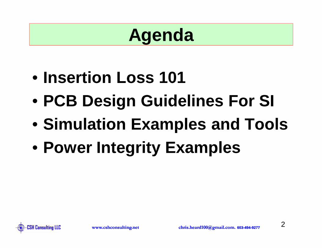
Agenda
• Insertion Loss 101• PCB Design Guidelines For SI• Simulation Examples and Tools• Power Integrity Examples

[email protected]. 603-494-9277www.cshconsulting.net [email protected]. 603-494-9277www.cshconsulting.net
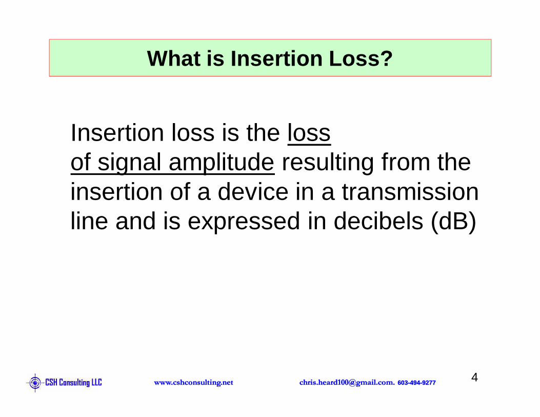
What is Insertion Loss?
Insertion loss is the loss of signal amplitude resulting from the insertion of a device in a transmission line and is expressed in decibels (dB)
[email protected]. 603-494-9277www.cshconsulting.net [email protected]. 603-494-9277www.cshconsulting.net
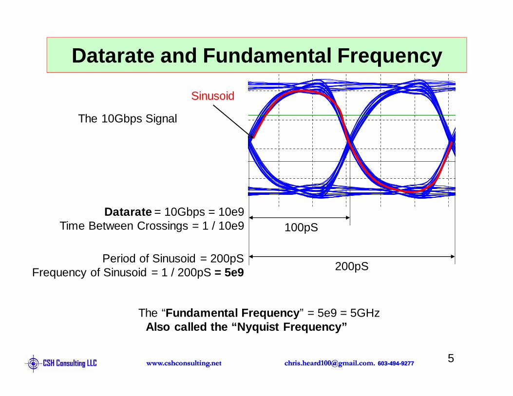
Datarate and Fundamental Frequency
200pS
The 10Gbps Signal
100pSDatarate = 10Gbps = 10e9
Time Between Crossings = 1 / 10e9
Period of Sinusoid = 200pSFrequency of Sinusoid = 1 / 200pS = 5e9
The “Fundamental Frequency ” = 5e9 = 5GHzAlso called the “Nyquist Frequency”
Sinusoid
[email protected]. 603-494-9277www.cshconsulting.net [email protected]. 603-494-9277www.cshconsulting.net
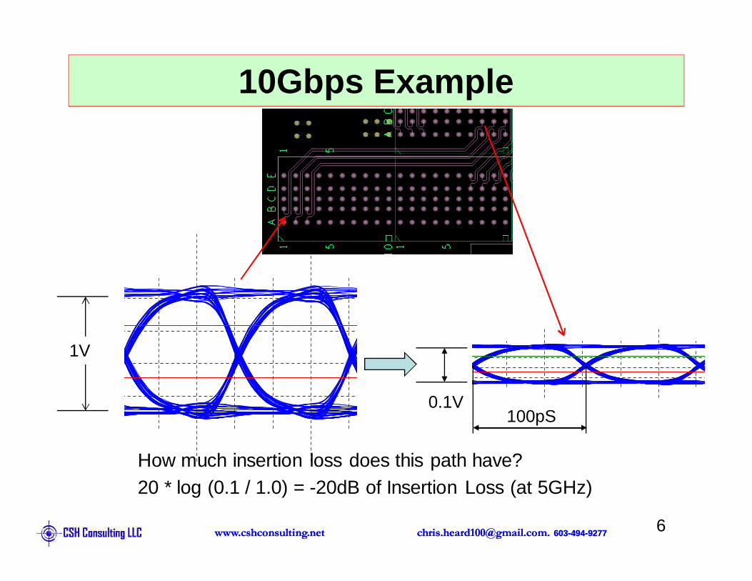
10Gbps Example
How much insertion loss does this path have?20 * log (0.1 / 1.0) = -20dB of Insertion Loss (at 5GHz)
1V
0.1V100pS

[email protected]. 603-494-9277www.cshconsulting.net [email protected]. 603-494-9277www.cshconsulting.net
Voltage vs Material in Volts
0.00
0.20
0.40
0.60
0.80
1.00
1.20
0.0 2.0 4.0 6.0 8.0 10.0 12.0 14.0 16.0 18.0 20.0 22.0 24.0 26.0 28.0 30.0 32.0 34.0 36.0 38.0 40.0
Volts
Frequency (GHz)
FR4 Hight Tg Nelco 4000-13 Megtron-6
FR4: 0.1VMeg6: 0.4V(4x better)
FR4
Nelco 4000-13
Megtron-6

[email protected]. 603-494-9277www.cshconsulting.net [email protected]. 603-494-9277www.cshconsulting.net
Loss vs Material in dB
-20.0 dB
5.0 GHz
-50
-45
-40
-35
-30
-25
-20
-15
-10
-5
0
0.0 2.0 4.0 6.0 8.0 10.0 12.0 14.0 16.0 18.0 20.0 22.0 24.0 26.0 28.0 30.0 32.0 34.0 36.0 38.0 40.0
Loss
(dB
)
Frequency (GHz)
Loss vs FrequencyFR4 High Tg Nelco 4000-13 Megtron-6
FR4: -20dBMeg6: -8dB(12dB better)
FR4 Nelco 4000-13
Megtron-6

[email protected]. 603-494-9277www.cshconsulting.net 10
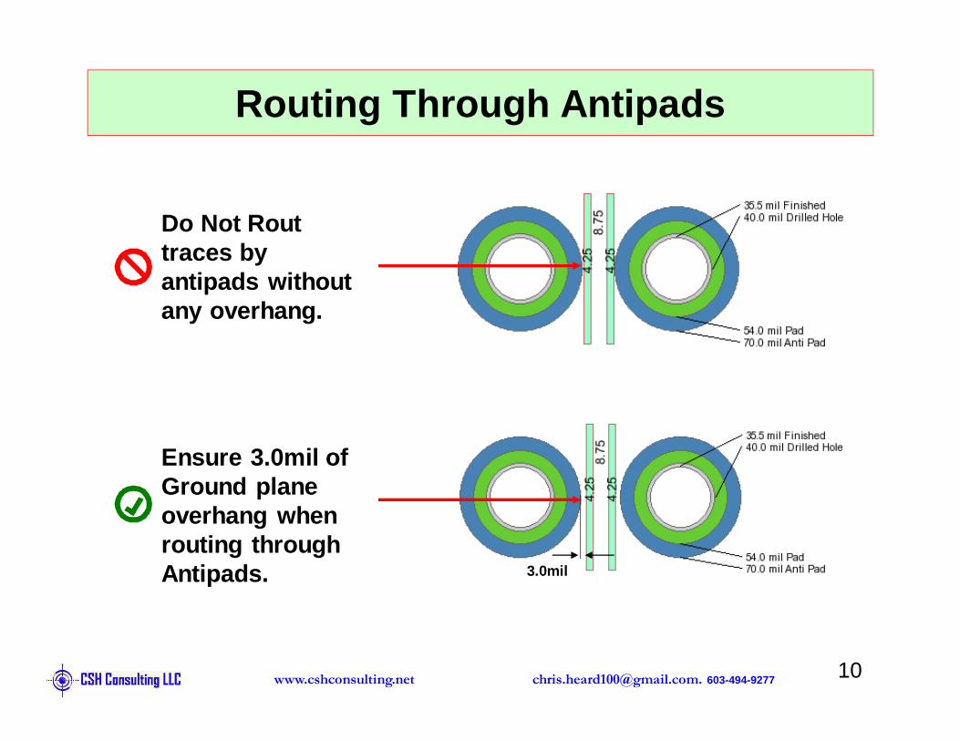
Routing Through Antipads
Do Not Rout traces by antipads without any overhang.
Ensure 3.0mil of Ground plane overhang when routing through Antipads. 3.0mil
[email protected]. 603-494-9277www.cshconsulting.net 11
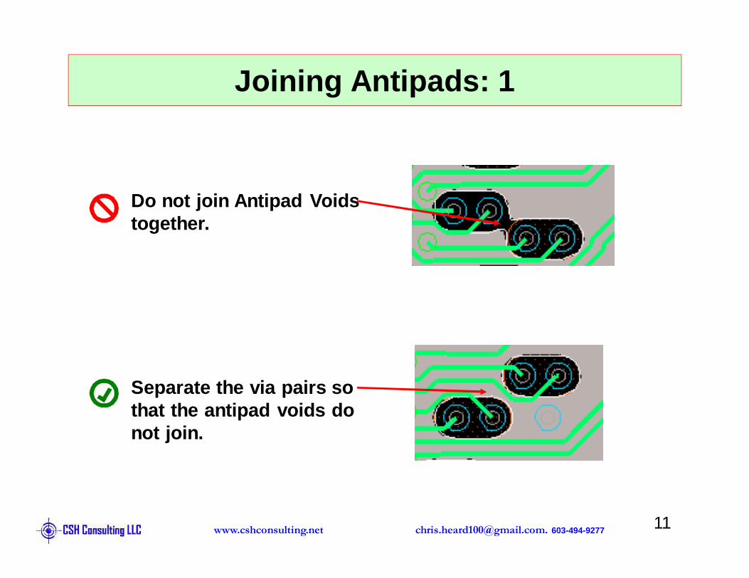
Joining Antipads: 1
Do not join Antipad Voids together.
Separate the via pairs so that the antipad voids do not join.

[email protected]. 603-494-9277www.cshconsulting.net 12
P N P
Joining Antipads: 2IPASS Connector
In this case the space between P and N signals is larger than the space to the next pair. This will increase crosstalk between pairs.
Arrange pins in a G-S-S-G format. Use the ground pins to achieve isolation between diff pairs.
[email protected]. 603-494-9277www.cshconsulting.net 13
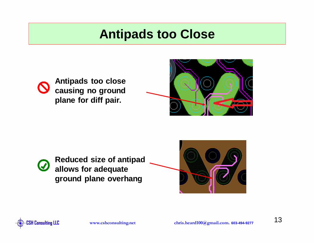
Antipads too Close
Antipads too close causing no ground plane for diff pair.
Reduced size of antipad allows for adequate ground plane overhang
[email protected]. 603-494-9277www.cshconsulting.net 14
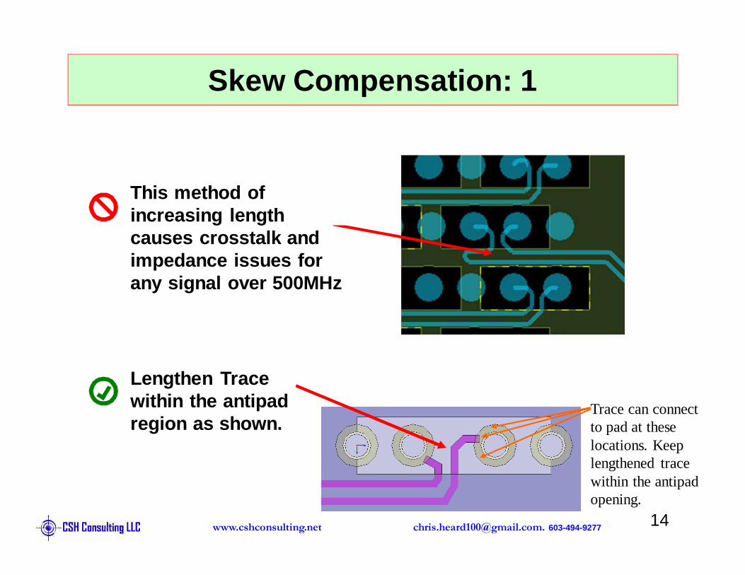
Skew Compensation: 1
This method of increasing length causes crosstalk and impedance issues for any signal over 500MHz
Lengthen Trace within the antipad region as shown.
Trace can connect to pad at these locations. Keep lengthened trace within the antipad opening.
[email protected]. 603-494-9277www.cshconsulting.net 15
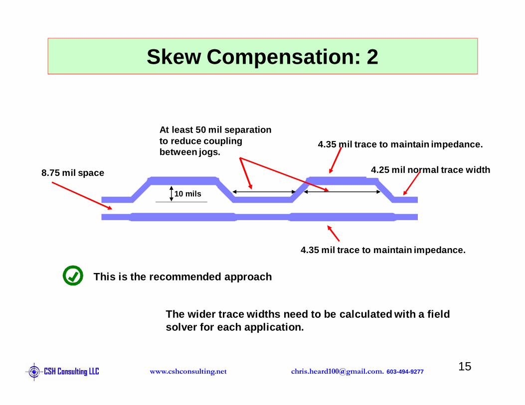
Skew Compensation: 2
At least 50 mil separation to reduce coupling between jogs.
4.35 mil trace to maintain impedance.
4.35 mil trace to maintain impedance.
4.25 mil normal trace width
10 mils
8.75 mil space
This is the recommended approach
The wider trace widths need to be calculated with a field solver for each application.
[email protected]. 603-494-9277www.cshconsulting.net 16
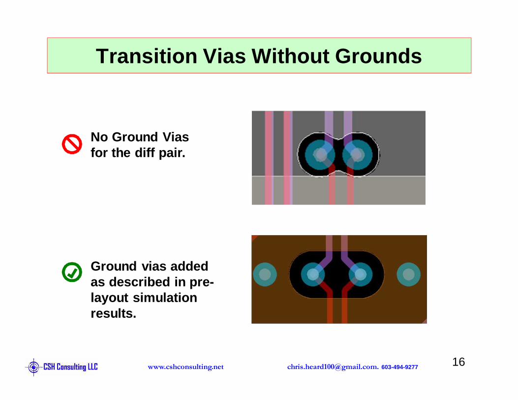
Transition Vias Without Grounds
No Ground Vias for the diff pair.
Ground vias added as described in pre-layout simulation results.
[email protected]. 603-494-9277www.cshconsulting.net 17
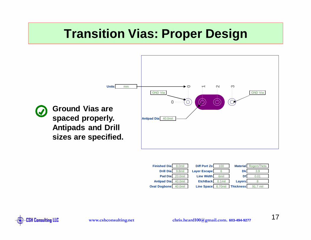
Transition Vias: Proper Design
0
0 1 2 3
Oval Dogbone 40.0mil
Antipad Dia 40.0mil
Pad Dia 20.0mil
Drill Dia 9.8mil
Finished Dia 8.0mil
Line Space 6.70mil
EtchBack 0.1mil
Line Width 6mil
Layer Escape 6
Diff Port Zo 100
Thickness 91.7 mil
Layers 8
Df 0.01
Dk 3.9
Material RogersTheta
Units mm
Antipad Dia 40.0mil
GND Via GND Via
Ground Vias are spaced properly. Antipads and Drill sizes are specified.
[email protected]. 603-494-9277www.cshconsulting.net 18
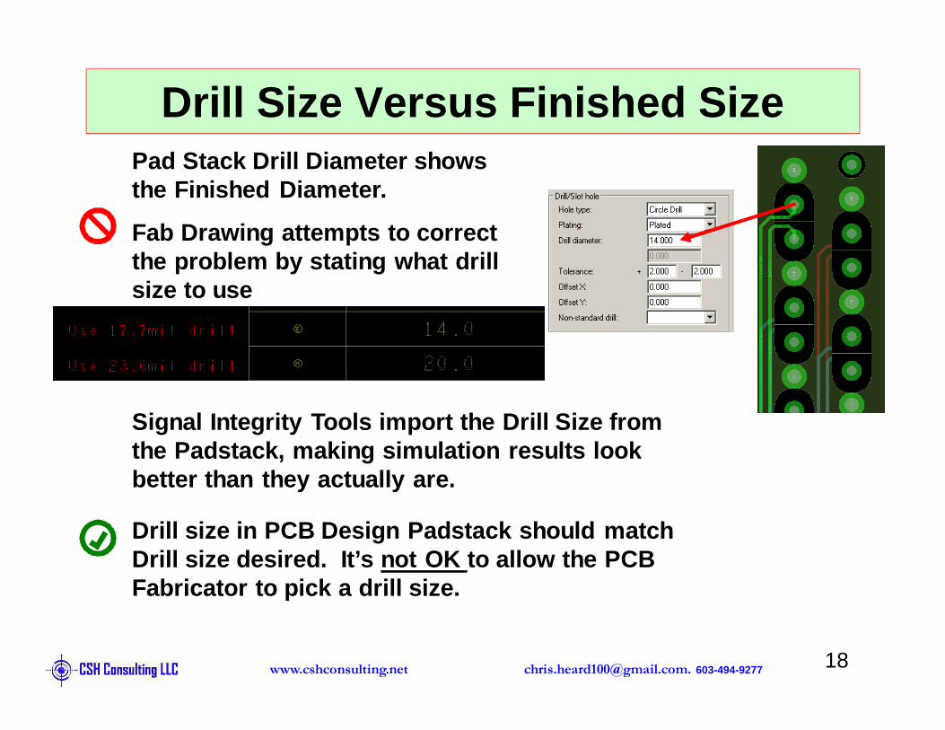
Drill Size Versus Finished SizePad Stack Drill Diameter shows the Finished Diameter.
Fab Drawing attempts to correct the problem by stating what drill size to use
Drill size in PCB Design Padstack should match Drill size desired. It’s not OK to allow the PCB Fabricator to pick a drill size.
Signal Integrity Tools import the Drill Size from the Padstack, making simulation results look better than they actually are.
[email protected]. 603-494-9277www.cshconsulting.net [email protected]. 603-494-9277www.cshconsulting.net
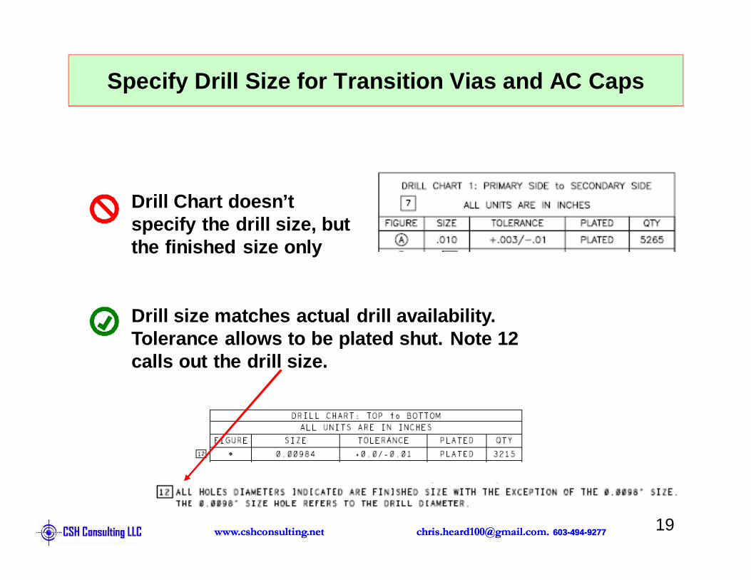
Specify Drill Size for Transition Vias and AC Caps
Drill Chart doesn’t specify the drill size, but the finished size only
Drill size matches actual drill availability. Tolerance allows to be plated shut. Note 12 calls out the drill size.
[email protected]. 603-494-9277www.cshconsulting.net 20
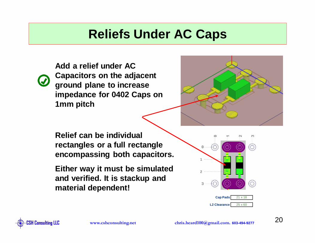
Reliefs Under AC Caps
Add a relief under AC Capacitors on the adjacent ground plane to increase impedance for 0402 Caps on 1mm pitch
Cap Pads 21 x 18
L2 Clearance 25 x 60
1
2
Relief can be individual rectangles or a full rectangle encompassing both capacitors.
Either way it must be simulated and verified. It is stackup and material dependent!
[email protected]. 603-494-9277www.cshconsulting.net 21
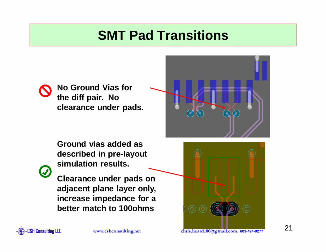
SMT Pad Transitions
No Ground Vias for the diff pair. No clearance under pads.
Ground vias added as described in pre-layout simulation results.
Clearance under pads on adjacent plane layer only, increase impedance for a better match to 100ohms
[email protected]. 603-494-9277www.cshconsulting.net 22
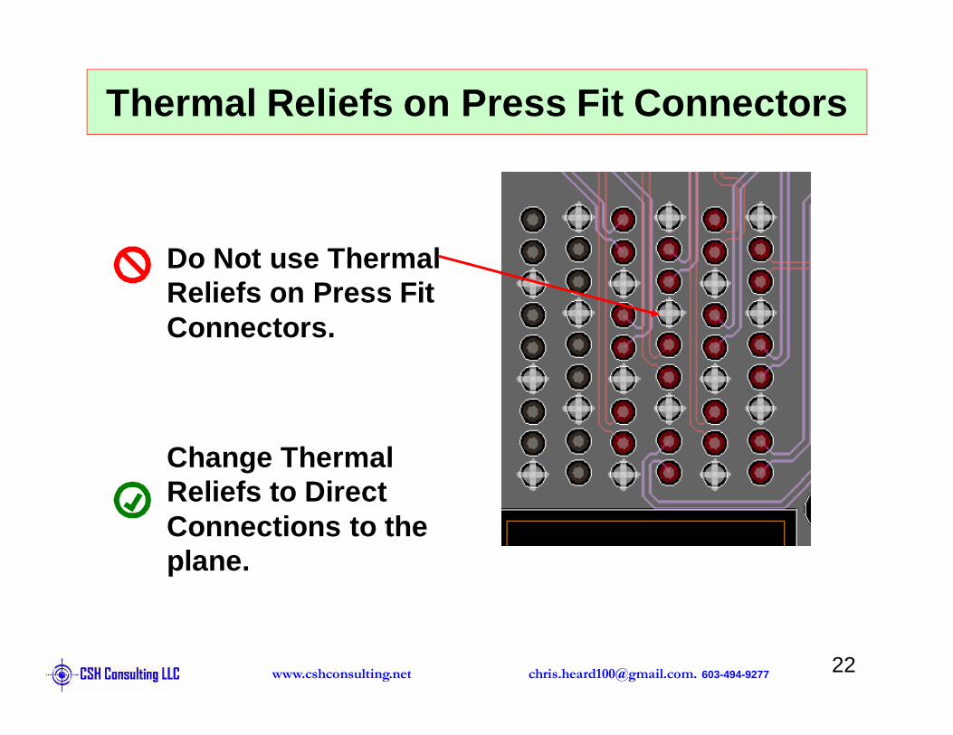
Thermal Reliefs on Press Fit Connectors
Do Not use Thermal Reliefs on Press Fit Connectors.
Change Thermal Reliefs to Direct Connections to the plane.

[email protected]. 603-494-9277www.cshconsulting.net 23
Rectangular or Oval Antipads on High Speed Connectors
Do Not use simple round antipads on high speed connectors
(Example: AirMax)
Change to rectangular or oval shape described in pre-layout simulation results.
[email protected]. 603-494-9277www.cshconsulting.net 24
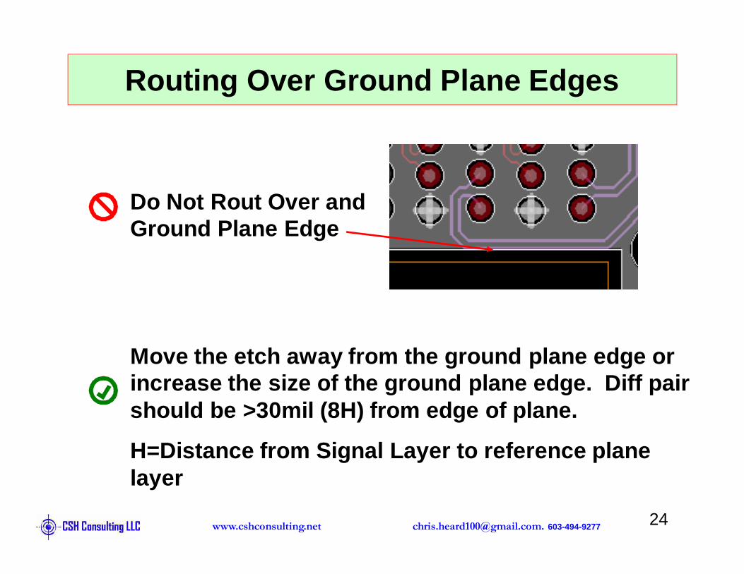
Routing Over Ground Plane Edges
Do Not Rout Over and Ground Plane Edge
Move the etch away from the ground plane edge or increase the size of the ground plane edge. Diff pa ir should be >30mil (8H) from edge of plane.
H=Distance from Signal Layer to reference plane layer
[email protected]. 603-494-9277www.cshconsulting.net 25
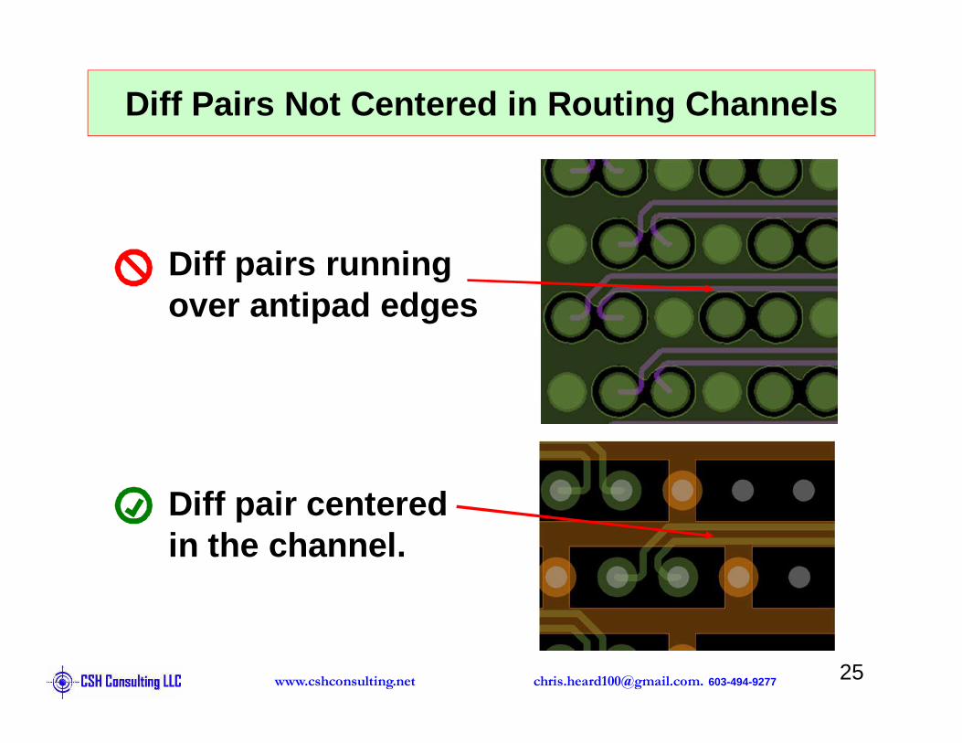
Diff Pairs Not Centered in Routing Channels
Diff pairs running over antipad edges
Diff pair centered in the channel.
[email protected]. 603-494-9277www.cshconsulting.net 26
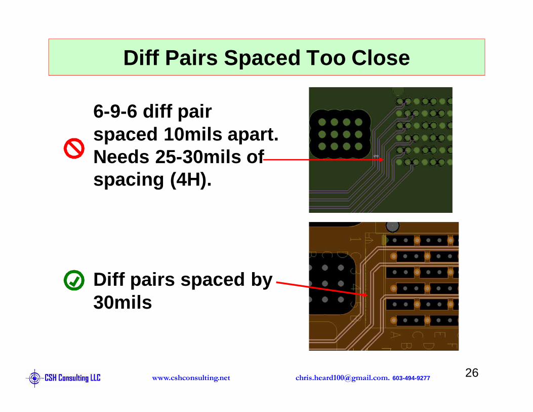
Diff Pairs Spaced Too Close
6-9-6 diff pair spaced 10mils apart. Needs 25-30mils of spacing (4H).
Diff pairs spaced by 30mils

[email protected]. 603-494-9277www.cshconsulting.net 27
Take Advantage of “Unused” Ground Planes
Move diff pairs up to adjacent channel to avoid the nearby Tx pair and to make use of a better ground reference.
Diff pairs moved away from nearby oval antipads to minimize coupling to other BGA signal pads.

[email protected]. 603-494-9277www.cshconsulting.net 28
Diff Pair Spacing on Top and Bottom Layers
Microstrip surface pairs are 12mil between P and N. Diff pairs are spaced 16mil apart. This causes lots of crosstalk.
They need to be 50-75mil apart! (10H)
Move diff pairs to inner layers and use closer spacing between P and N (8mil).
Or use 50-75mil spacing between pairs on the surface.
12.0mil
16.0mil

[email protected]. 603-494-9277www.cshconsulting.net 29
Splitting Up Diff Pairs: 1
Avoid separating diff pairs to get around vias.
Keep the pair coupled together at all times.
[email protected]. 603-494-9277www.cshconsulting.net 30
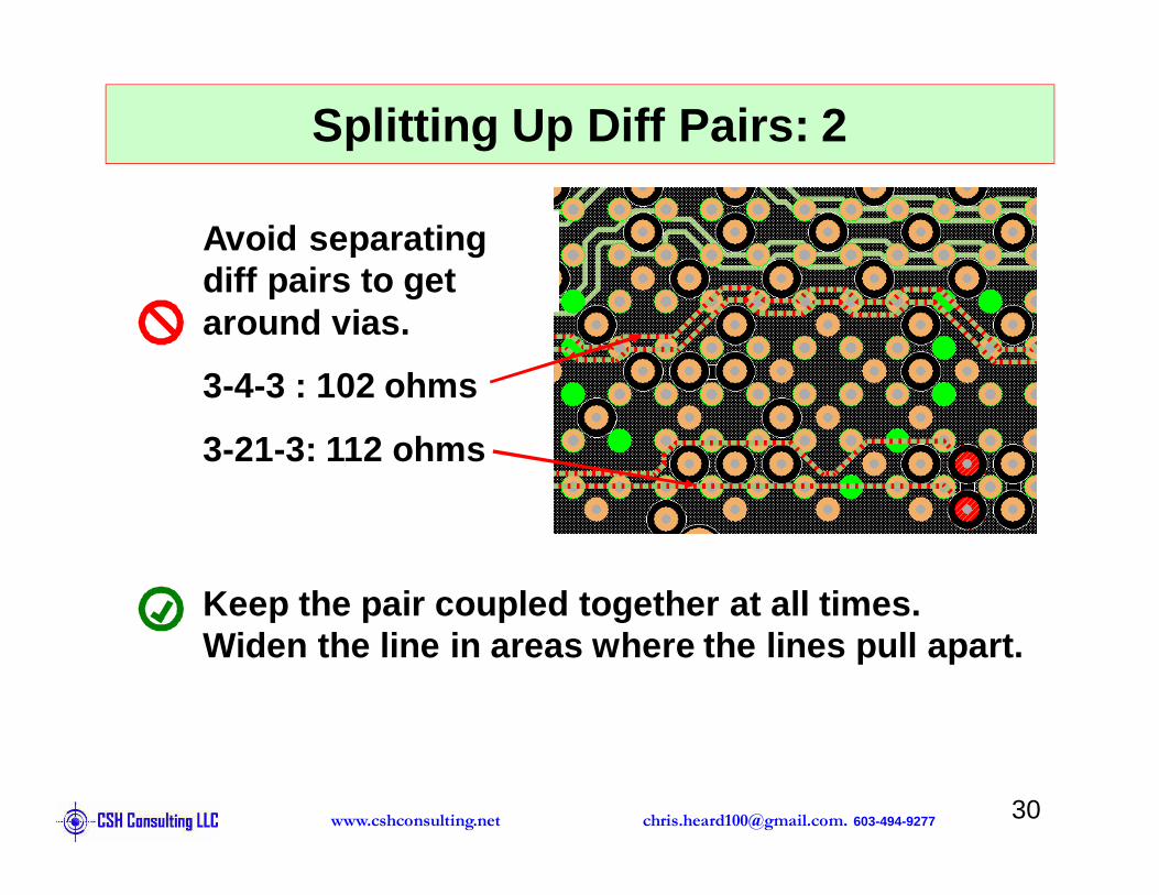
Splitting Up Diff Pairs: 2
Avoid separating diff pairs to get around vias.
3-4-3 : 102 ohms
3-21-3: 112 ohms
Keep the pair coupled together at all times. Widen the line in areas where the lines pull apart.

[email protected]. 603-494-9277www.cshconsulting.net 31
Serpentine Spacing
Serpentines are 13mils apart.
Diff pairs are 8.75mils apart.
This causes about 0.2% of crosstalk on to itself, which is too high.
Increase spacing to 17mils or more (4H)
H=Distance from Signal Layer to reference plane lay er
[email protected]. 603-494-9277www.cshconsulting.net 32
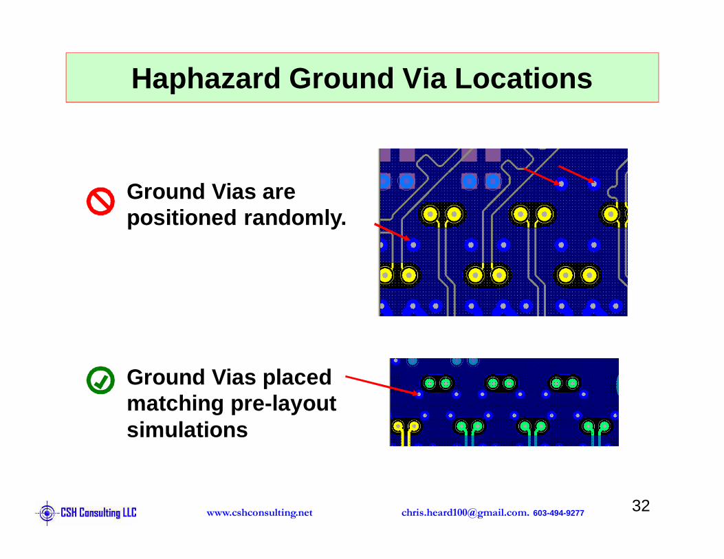
Haphazard Ground Via Locations
Ground Vias are positioned randomly.
Ground Vias placed matching pre-layout simulations
[email protected]. 603-494-9277www.cshconsulting.net 33
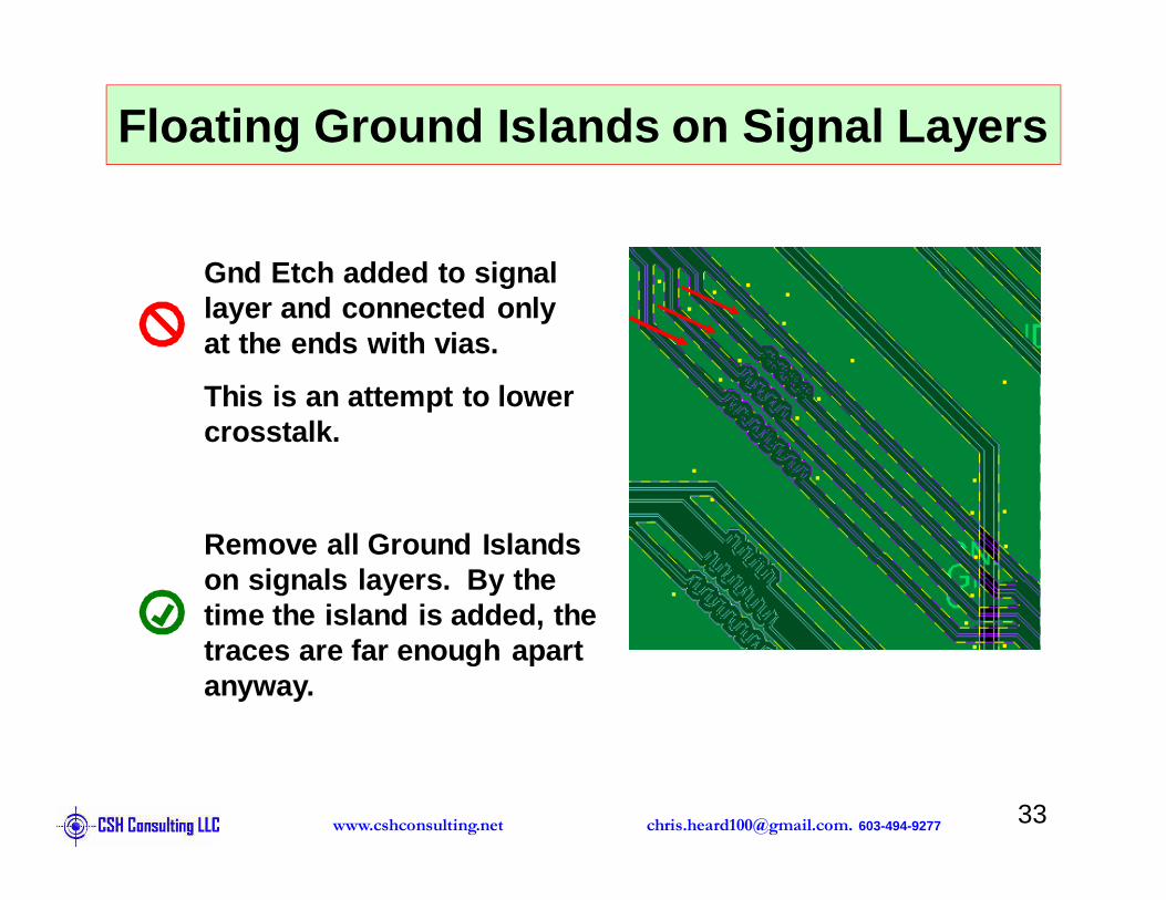
Floating Ground Islands on Signal Layers
Gnd Etch added to signal layer and connected only at the ends with vias.
This is an attempt to lower crosstalk.
Remove all Ground Islands on signals layers. By the time the island is added, the traces are far enough apart anyway.

[email protected]. 603-494-9277www.cshconsulting.net 34
Routing Over Splits: 1
Traces crossing over a split in the ground plane on an adjacent layer
Remove the split in the ground plane or move the traces to a layer that has a continuous plane.
[email protected]. 603-494-9277www.cshconsulting.net 35
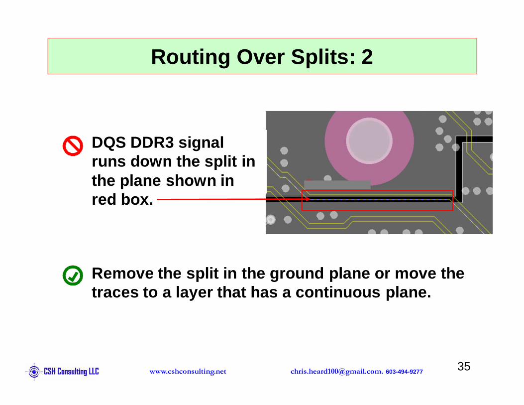
Routing Over Splits: 2
DQS DDR3 signal runs down the split in the plane shown in red box.
Remove the split in the ground plane or move the traces to a layer that has a continuous plane.
[email protected]. 603-494-9277www.cshconsulting.net 36
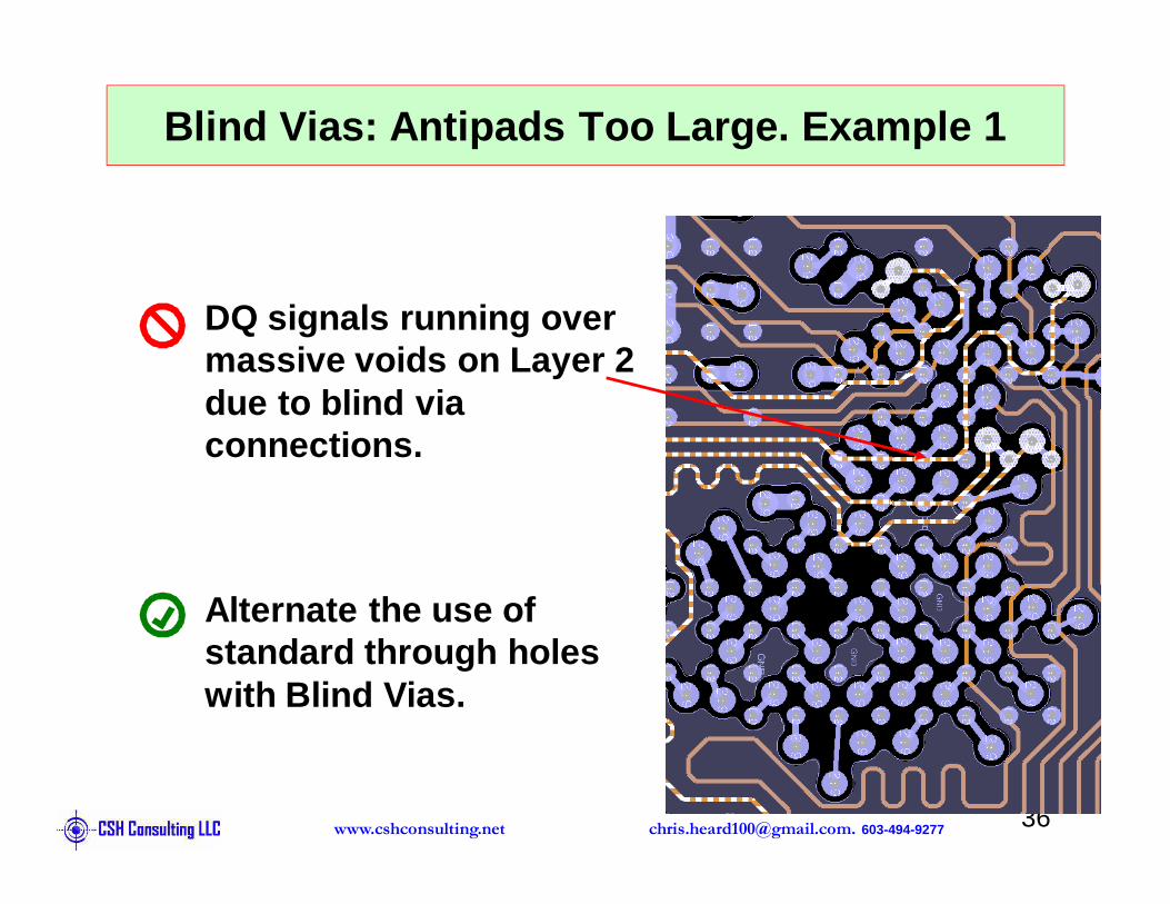
Blind Vias: Antipads Too Large. Example 1
DQ signals running over massive voids on Layer 2 due to blind via connections.
Alternate the use of standard through holes with Blind Vias.
[email protected]. 603-494-9277www.cshconsulting.net 37
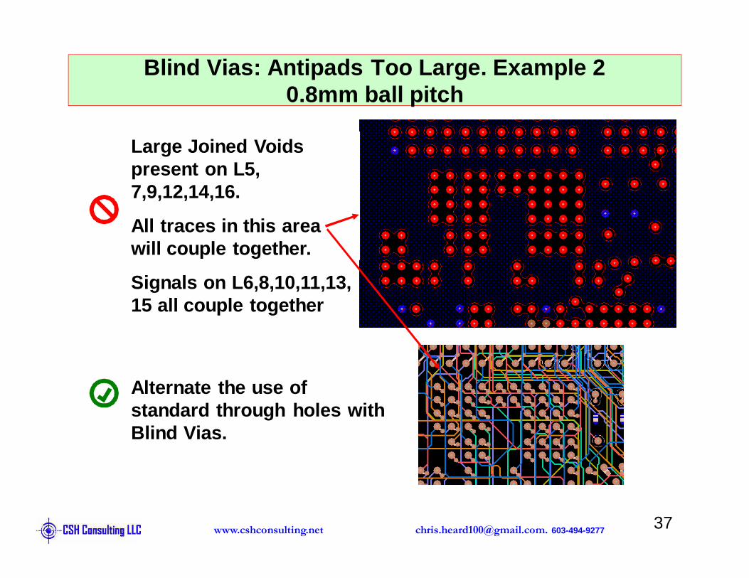
Blind Vias: Antipads Too Large. Example 20.8mm ball pitch
Large Joined Voids present on L5, 7,9,12,14,16.
All traces in this area will couple together.
Signals on L6,8,10,11,13, 15 all couple together
Alternate the use of standard through holes with Blind Vias.
[email protected]. 603-494-9277www.cshconsulting.net [email protected]. 603-494-9277www.cshconsulting.net
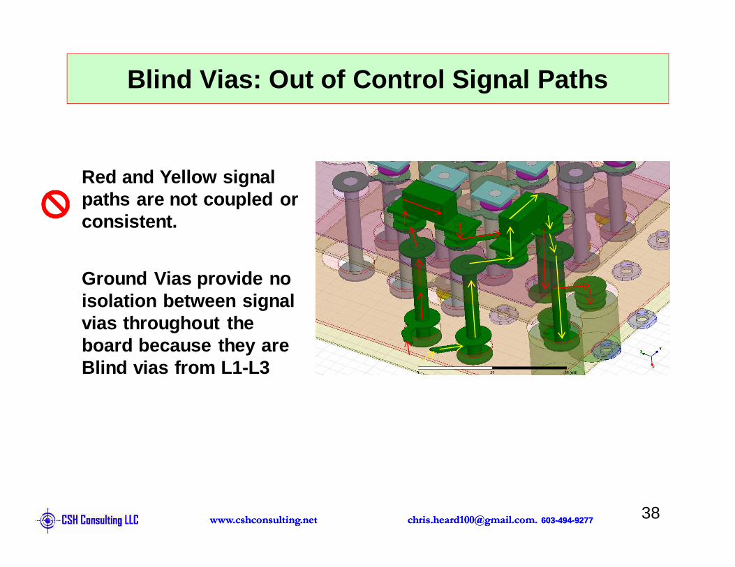
Blind Vias: Out of Control Signal Paths
Red and Yellow signal paths are not coupled or consistent.
Ground Vias provide no isolation between signal vias throughout the board because they are Blind vias from L1-L3
[email protected]. 603-494-9277www.cshconsulting.net 39
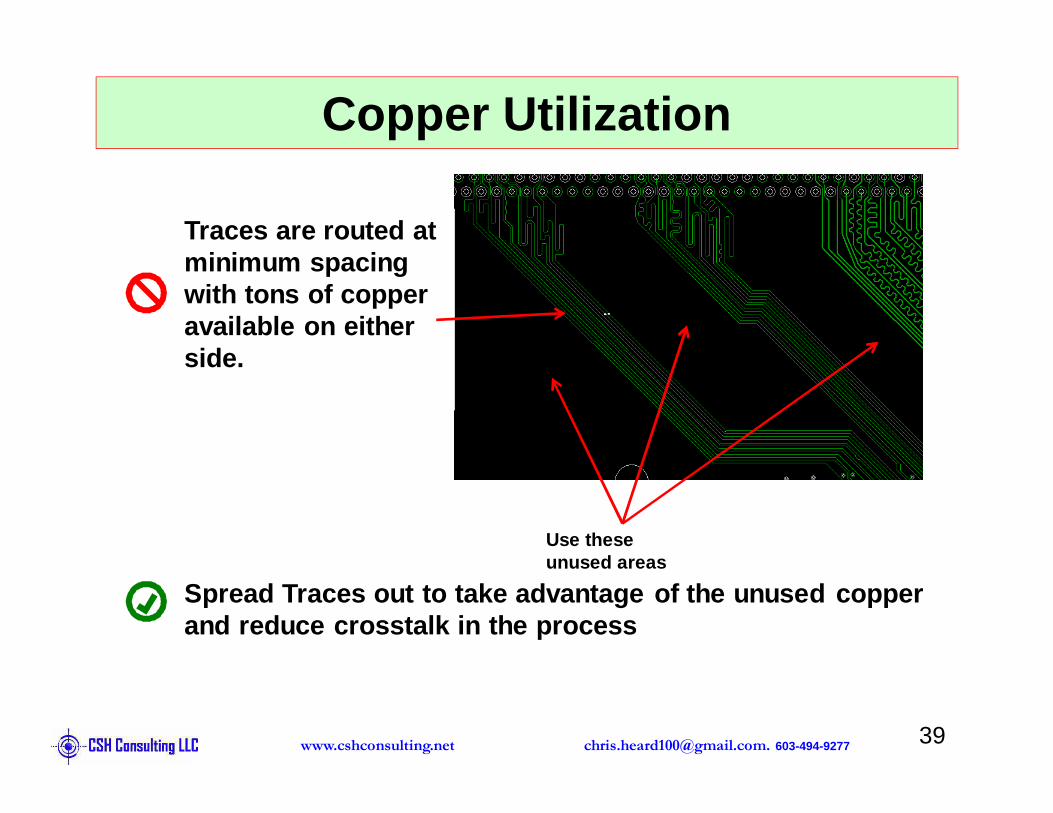
Copper Utilization
Traces are routed at minimum spacing with tons of copper available on either side.
Spread Traces out to take advantage of the unused c opper and reduce crosstalk in the process
Use these unused areas
[email protected]. 603-494-9277www.cshconsulting.net 40
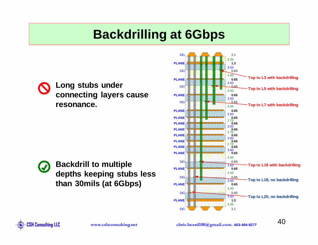
Backdrilling at 6Gbps
Long stubs under connecting layers cause resonance.
Backdrill to multiple depths keeping stubs less than 30mils (at 6Gbps)
SIG 2.13.35
PLANE 1.33.50
SIG 0.654.45
PLANE 0.653.50
SIG 0.654.45
PLANE 0.653.50
SIG 0.654.45
PLANE 0.653.50
PLANE 0.652.70
PLANE 0.653.00
PLANE 0.652.70
PLANE 0.653.00
PLANE 0.652.70
PLANE 0.653.00
PLANE 0.654.45
SIG 0.653.50
PLANE 0.654.45
SIG 0.653.50
PLANE 0.654.45
SIG 0.653.50
PLANE 1.33.35
SIG 2.1
Top to L3 with backdrilling
Top to L5 with backdrilling
Top to L7 with backdrilling
Top to L16 with backdrilling
Top to L18, no backdrilling
Top to L20, no backdrilling
[email protected]. 603-494-9277www.cshconsulting.net
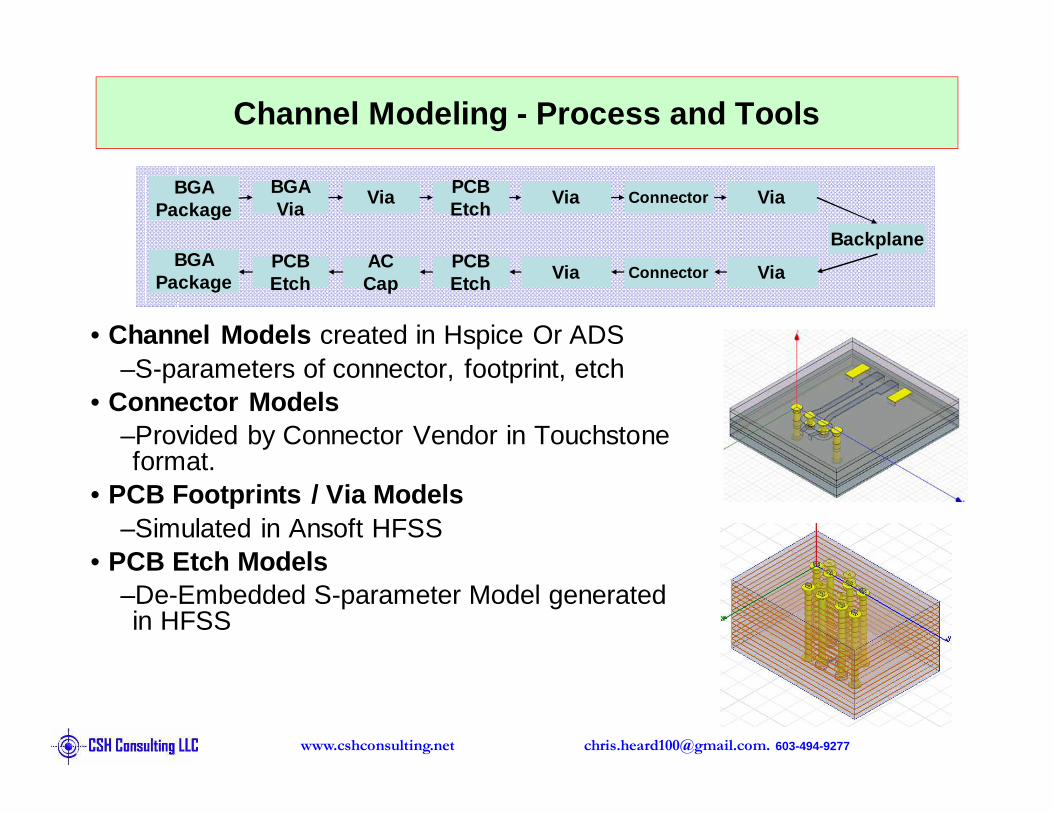
Channel Modeling - Process and Tools
• Channel Models created in Hspice Or ADS–S-parameters of connector, footprint, etch
• Connector Models–Provided by Connector Vendor in Touchstone format.
• PCB Footprints / Via Models–Simulated in Ansoft HFSS
• PCB Etch Models–De-Embedded S-parameter Model generated in HFSS
BGA Package
BGA Via
PCB Etch
Via Via Connector Via
BackplanePCB Etch
PCB Etch
AC Cap
Via ViaConnectorBGA
Package
[email protected]. 603-494-9277www.cshconsulting.net [email protected]. 603-494-9277www.cshconsulting.net
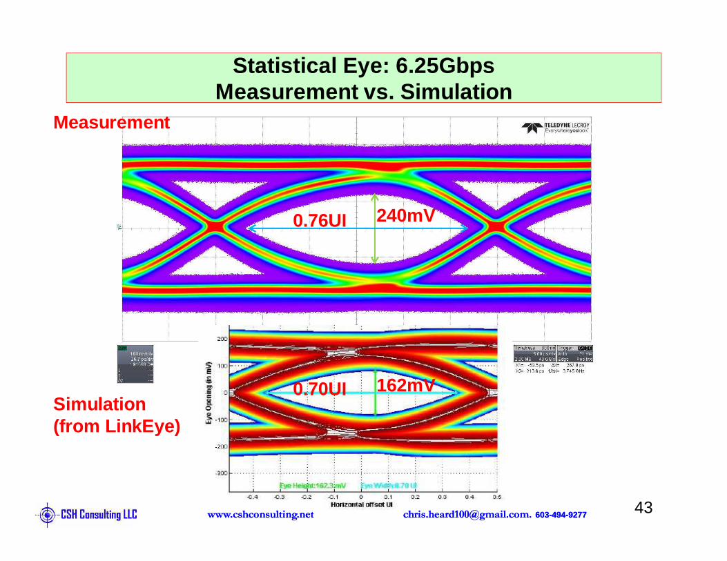
Statistical Eye: 6.25GbpsMeasurement vs. Simulation
Measurement
Simulation (from LinkEye)
240mV0.76UI
162mV0.70UI
[email protected]. 603-494-9277www.cshconsulting.net 44
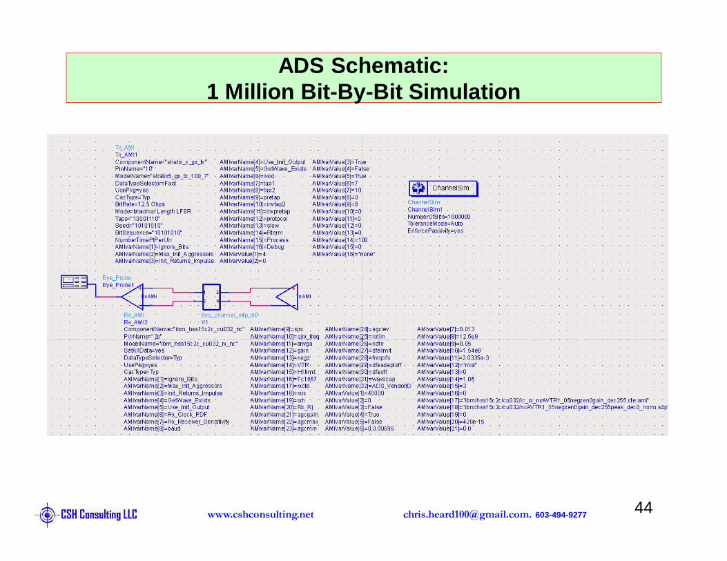
ADS Schematic:1 Million Bit-By-Bit Simulation
[email protected]. 603-494-9277www.cshconsulting.net 45
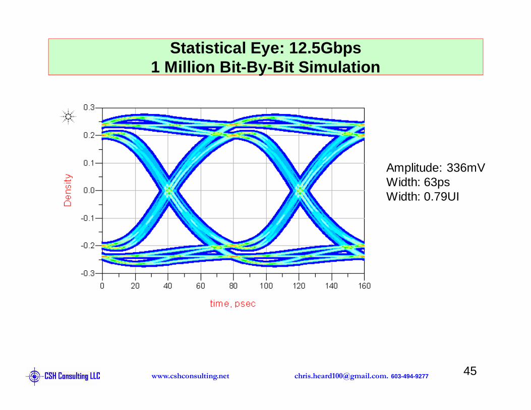
Statistical Eye: 12.5Gbps1 Million Bit-By-Bit Simulation
Amplitude: 336mVWidth: 63psWidth: 0.79UI
[email protected]. 603-494-9277www.cshconsulting.net 47
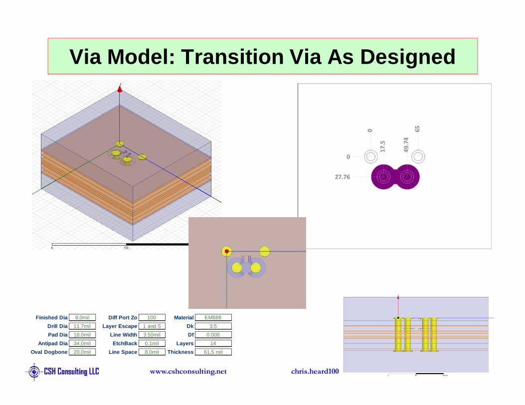
Via Model: Transition Via As Designed
Oval Dogbone 20.0mil
Antipad Dia 34.0mil
Pad Dia 18.0mil
Drill Dia 11.7mil
Finished Dia 8.0mil
Line Space 8.0mil
EtchBack 0.1mil
Line Width 3.50mil
Layer Escape 1 and 5
Diff Port Zo 100
Thickness 61.5 mil
Layers 14
Df 0.008
Dk 3.5
Material EM888
[email protected]. 603-494-9277www.cshconsulting.net 48
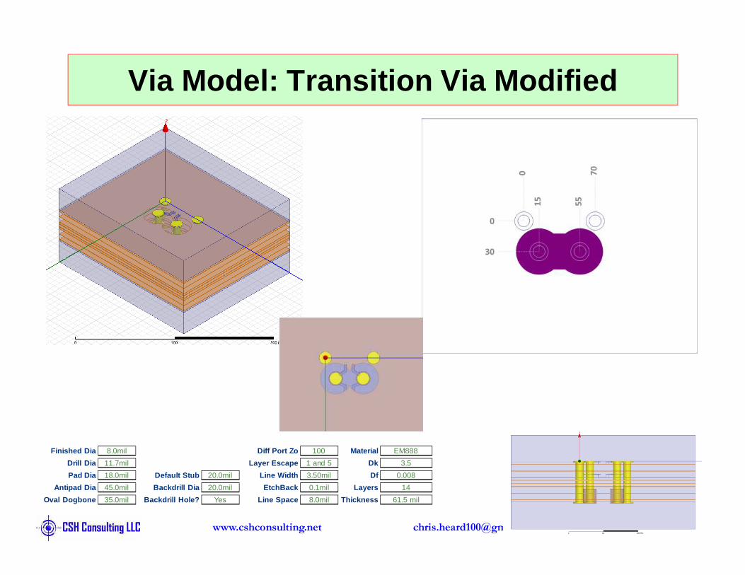
Via Model: Transition Via Modified
Oval Dogbone 35.0mil
Antipad Dia 45.0mil
Pad Dia 18.0mil
Drill Dia 11.7mil
Finished Dia 8.0mil
Backdrill Hole? Yes
Backdrill Dia 20.0mil
Default Stub 20.0mil
Line Space 8.0mil
EtchBack 0.1mil
Line Width 3.50mil
Layer Escape 1 and 5
Diff Port Zo 100
Thickness 61.5 mil
Layers 14
Df 0.008
Dk 3.5
Material EM888
[email protected]. 603-494-9277www.cshconsulting.net 49
0 2 4 6 8 10 12 14 16 18 20-40
-35
-30
-25
-20
-15
-10
-5
0Differential Insertion and Return Loss: SEB1-TransVia
Frequency (GHz)
Mag
nitu
de (
dB)
sdd12
sdd11
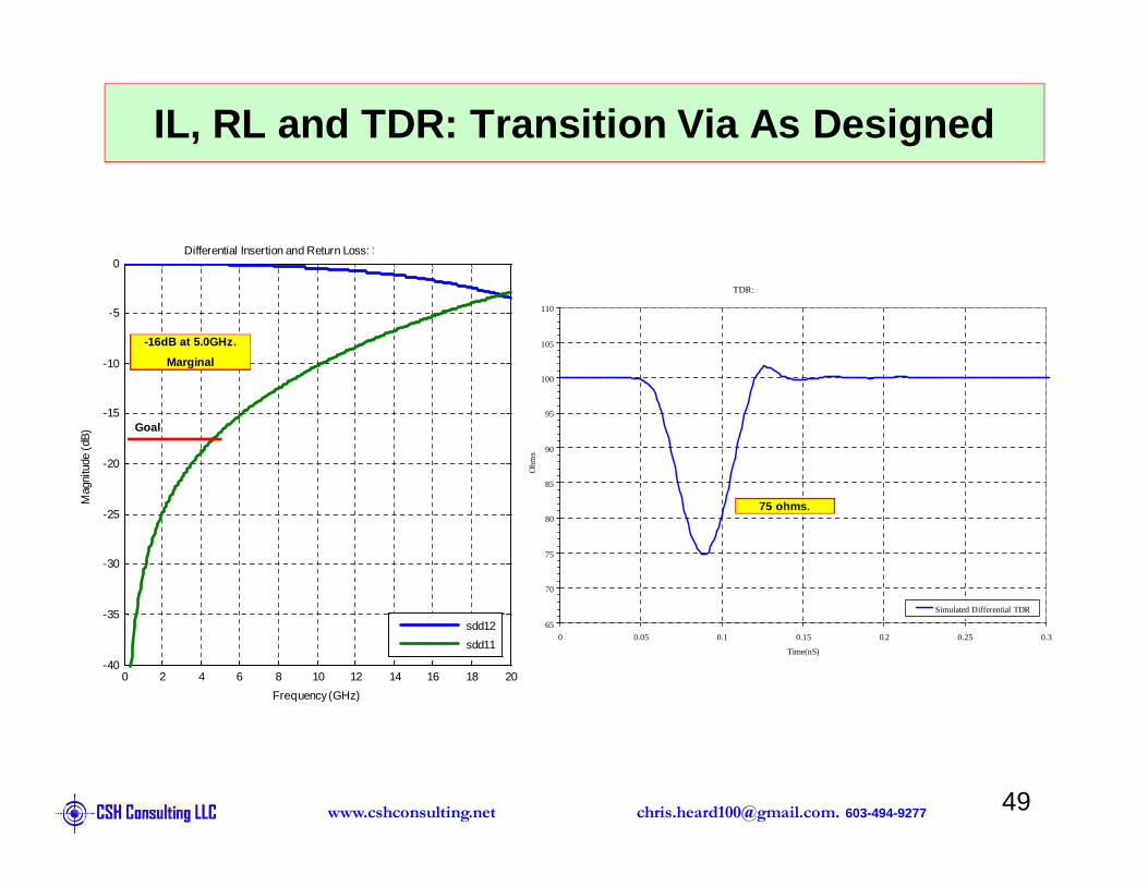
IL, RL and TDR: Transition Via As Designed
-16dB at 5.0GHz.
Marginal
TDR: SEB1-TransVia
65
70
75
80
85
90
95
100
105
110
0 0.05 0.1 0.15 0.2 0.25 0.3
Time(nS)
Simulated Differential TDR
Ohm
s
75 ohms.
Goal

[email protected]. 603-494-9277www.cshconsulting.net 50
0 2 4 6 8 10 12 14 16 18 20-40
-35
-30
-25
-20
-15
-10
-5
0Differential Insertion and Return Loss: SEB1-TransVia-R1
Frequency (GHz)
Mag
nitu
de (
dB)
sdd12
sdd11
IL, RL and TDR: Transition Via Modified
-38dB at 5.0GHz.
Excellent
TDR: SEB1-TransVia-R1
65
70
75
80
85
90
95
100
105
110
0 0.05 0.1 0.15 0.2 0.25 0.3
Time(nS)
Simulated Differential TDR
Ohm
s
95 ohms.Goal
[email protected]. 603-494-9277www.cshconsulting.net 51
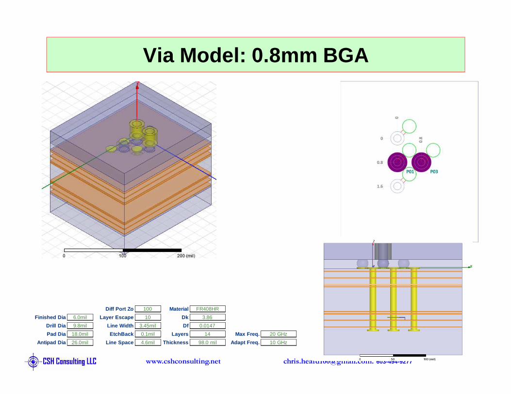
Via Model: 0.8mm BGA
Antipad Dia 26.0mil
Pad Dia 18.0mil
Drill Dia 9.8mil
Finished Dia 6.0mil
Line Space 4.6mil
EtchBack 0.1mil
Line Width 3.45mil
Layer Escape 10
Diff Port Zo 100
Thickness 98.0 mil
Layers 14
Df 0.0147
Dk 3.86
Material FR408HR
Adapt Freq. 10 GHz
Max Freq. 20 GHz
[email protected]. 603-494-9277www.cshconsulting.net 52
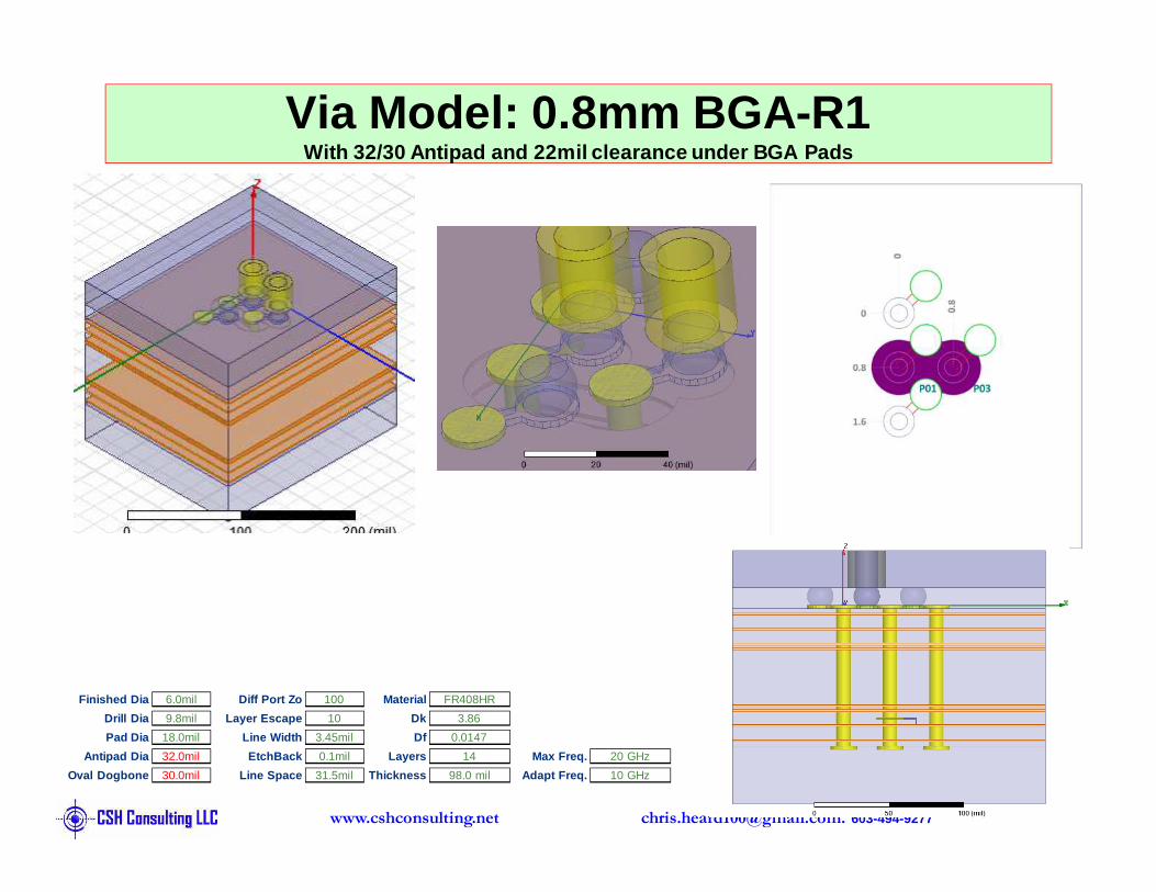
Via Model: 0.8mm BGA -R1With 32/30 Antipad and 22mil clearance under BGA Pa ds
Oval Dogbone 30.0mil
Antipad Dia 32.0mil
Pad Dia 18.0mil
Drill Dia 9.8mil
Finished Dia 6.0mil
Line Space 31.5mil
EtchBack 0.1mil
Line Width 3.45mil
Layer Escape 10
Diff Port Zo 100
Thickness 98.0 mil
Layers 14
Df 0.0147
Dk 3.86
Material FR408HR
Adapt Freq. 10 GHz
Max Freq. 20 GHz
[email protected]. 603-494-9277www.cshconsulting.net 53
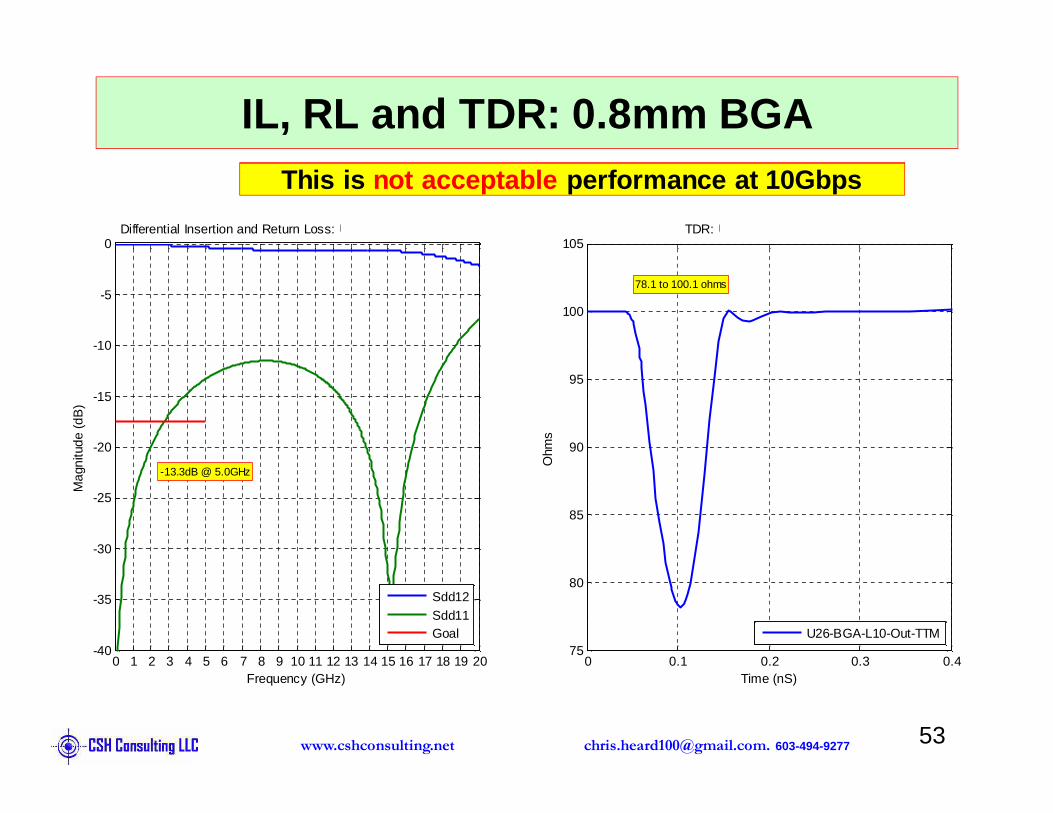
IL, RL and TDR: 0.8mm BGA
0 1 2 3 4 5 6 7 8 9 10 11 12 13 14 15 16 17 18 19 20-40
-35
-30
-25
-20
-15
-10
-5
0
Frequency (GHz)
Mag
nitu
de (
dB)
Differential Insertion and Return Loss: U26 BGA L10 Out TTM
-13.3dB @ 5.0GHz
Sdd12Sdd11Goal
0 0.1 0.2 0.3 0.475
80
85
90
95
100
105
Time (nS)
Ohm
s
78.1 to 100.1 ohms
TDR: U26-BGA-L10-Out-TTM
U26-BGA-L10-Out-TTM
This is not acceptable performance at 10Gbps
[email protected]. 603-494-9277www.cshconsulting.net 54
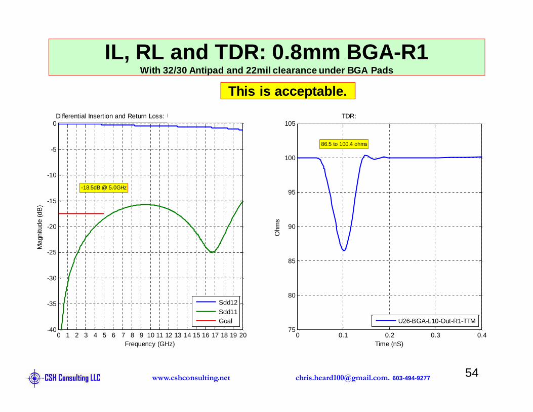
IL, RL and TDR: 0.8mm BGA -R1With 32/30 Antipad and 22mil clearance under BGA Pa ds
0 1 2 3 4 5 6 7 8 9 10 11 12 13 14 15 16 17 18 19 20-40
-35
-30
-25
-20
-15
-10
-5
0
Frequency (GHz)
Mag
nitu
de (
dB)
Differential Insertion and Return Loss: U26 BGA L10 Out R1 TTM
-18.5dB @ 5.0GHz
Sdd12Sdd11Goal
0 0.1 0.2 0.3 0.475
80
85
90
95
100
105
Time (nS)
Ohm
s
86.5 to 100.4 ohms
TDR: U26-BGA-L10-Out-R1-TTM
U26-BGA-L10-Out-R1-TTM
This is acceptable.
[email protected]. 603-494-9277www.cshconsulting.net 56
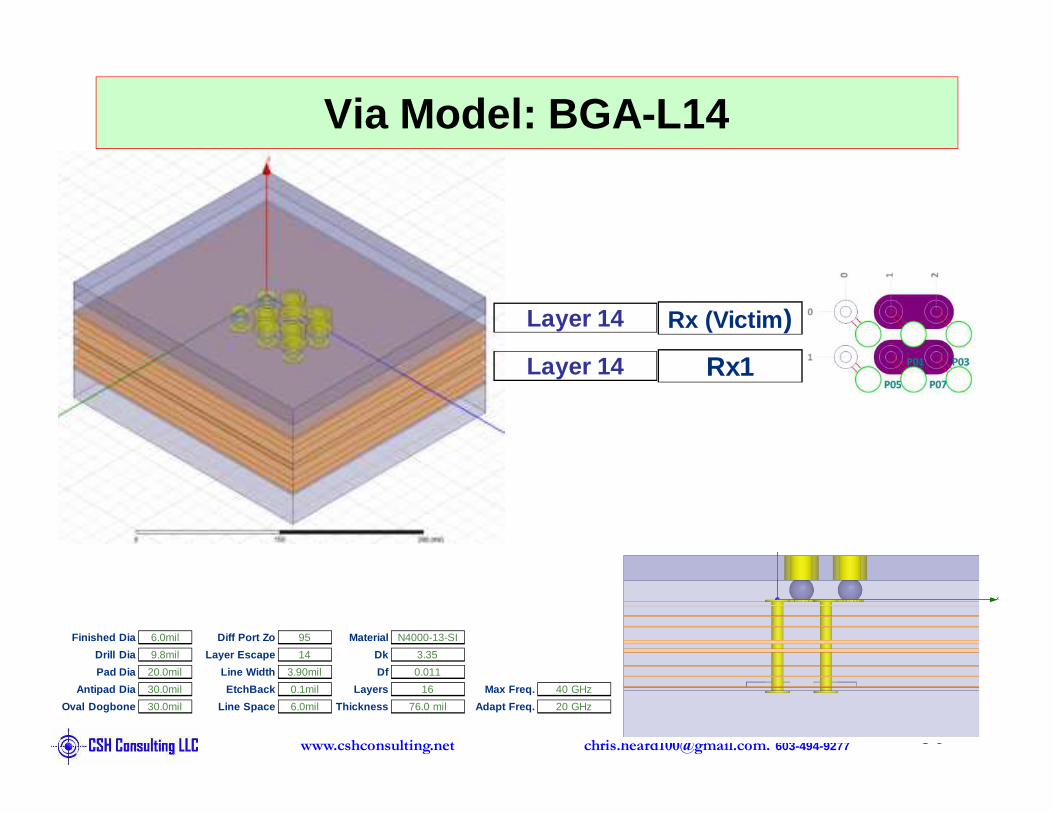
Via Model: BGA -L14
Oval Dogbone 30.0mil
Antipad Dia 30.0mil
Pad Dia 20.0mil
Drill Dia 9.8mil
Finished Dia 6.0mil
Line Space 6.0mil
EtchBack 0.1mil
Line Width 3.90mil
Layer Escape 14
Diff Port Zo 95
Thickness 76.0 mil
Layers 16
Df 0.011
Dk 3.35
Material N4000-13-SI
Adapt Freq. 20 GHz
Max Freq. 40 GHz
Rx (Victim )
Rx1Layer 14
Layer 14
[email protected]. 603-494-9277www.cshconsulting.net 57
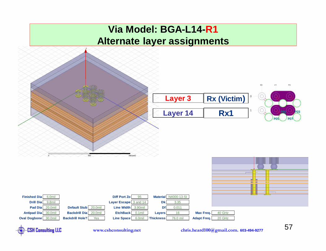
Via Model: BGA -L14-R1Alternate layer assignments
Oval Dogbone 30.0mil
Antipad Dia 30.0mil
Pad Dia 20.0mil
Drill Dia 9.8mil
Finished Dia 6.0mil
Backdrill Hole? Yes
Backdrill Dia 20.0mil
Default Stub 20.0mil
Line Space 6.0mil
EtchBack 0.1mil
Line Width 3.90mil
Layer Escape 3 and 14
Diff Port Zo 95
Thickness 76.0 mil
Layers 16
Df 0.011
Dk 3.35
Material N4000-13-SI
Adapt Freq. 20 GHz
Max Freq. 40 GHz
Rx (Victim )
Rx1Layer 14
Layer 3
[email protected]. 603-494-9277www.cshconsulting.net 58
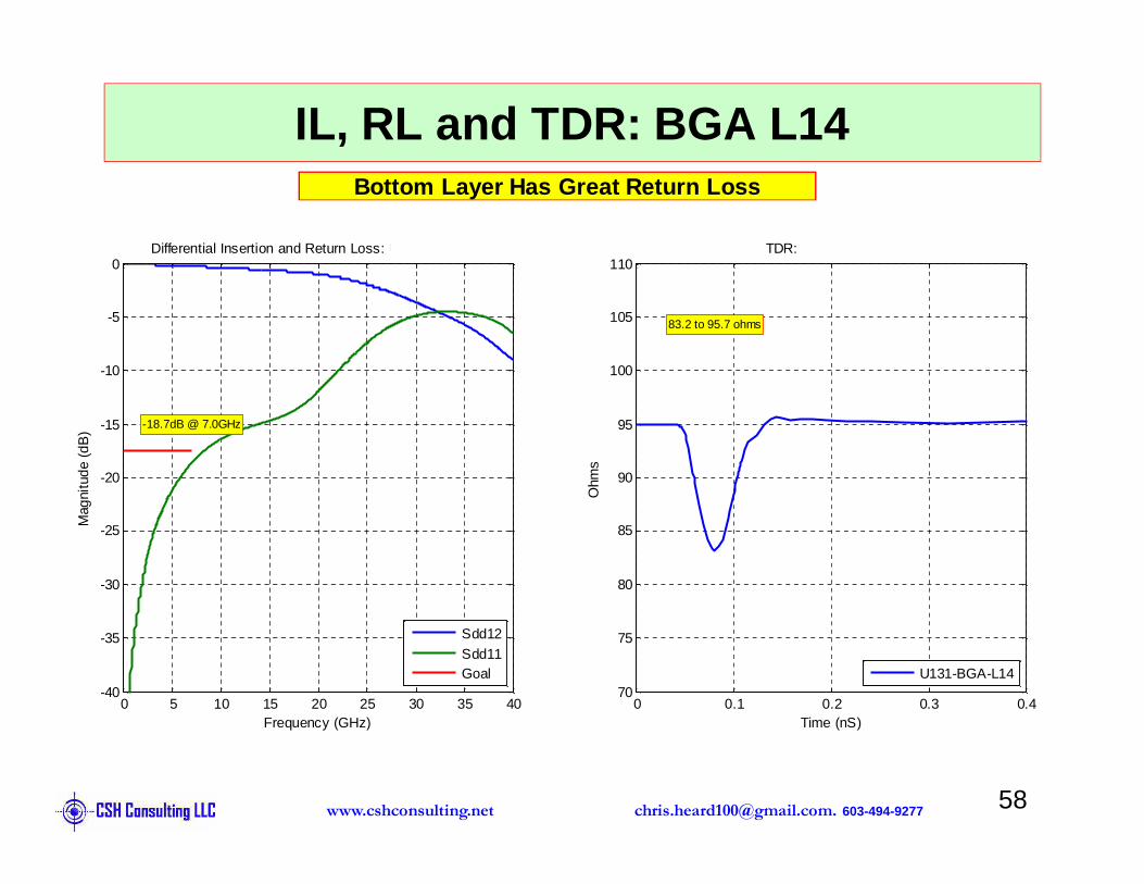
IL, RL and TDR: BGA L14
0 5 10 15 20 25 30 35 40-40
-35
-30
-25
-20
-15
-10
-5
0Differential Insertion and Return Loss: U131 BGA L14
-18.7dB @ 7.0GHz
Frequency (GHz)
Mag
nitu
de (
dB)
Sdd12Sdd11Goal
0 0.1 0.2 0.3 0.470
75
80
85
90
95
100
105
110
Time (nS)
Ohm
s
83.2 to 95.7 ohms
TDR: U131-BGA-L14
U131-BGA-L14
Bottom Layer Has Great Return Loss
[email protected]. 603-494-9277www.cshconsulting.net 59
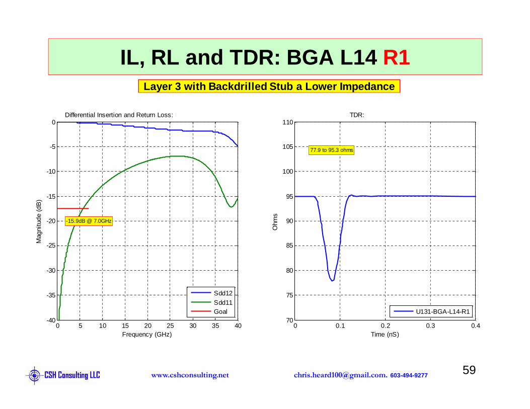
IL, RL and TDR: BGA L14 R1
0 5 10 15 20 25 30 35 40-40
-35
-30
-25
-20
-15
-10
-5
0Differential Insertion and Return Loss: U131 BGA L14 R1
-15.9dB @ 7.0GHz
Frequency (GHz)
Mag
nitu
de (
dB)
Sdd12Sdd11Goal
0 0.1 0.2 0.3 0.470
75
80
85
90
95
100
105
110
Time (nS)
Ohm
s
77.9 to 95.3 ohms
TDR: U131-BGA-L14-R1
U131-BGA-L14-R1
Layer 3 with Backdrilled Stub a Lower Impedance
[email protected]. 603-494-9277www.cshconsulting.net 60
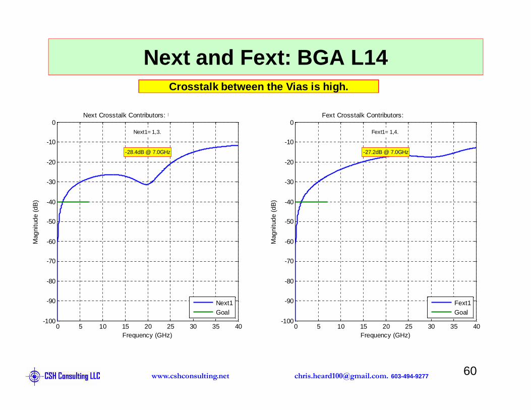
Next and Fext: BGA L14
0 5 10 15 20 25 30 35 40-100
-90
-80
-70
-60
-50
-40
-30
-20
-10
0Next Crosstalk Contributors: U131 BGA L14
-28.4dB @ 7.0GHz
Next1= 1,3.
Frequency (GHz)
Mag
nitu
de (
dB)
Next1Goal
0 5 10 15 20 25 30 35 40-100
-90
-80
-70
-60
-50
-40
-30
-20
-10
0Fext Crosstalk Contributors: U131 BGA L14
-27.2dB @ 7.0GHz
Fext1= 1,4.
Frequency (GHz)
Mag
nitu
de (
dB)
Fext1Goal
Crosstalk between the Vias is high.
[email protected]. 603-494-9277www.cshconsulting.net 61
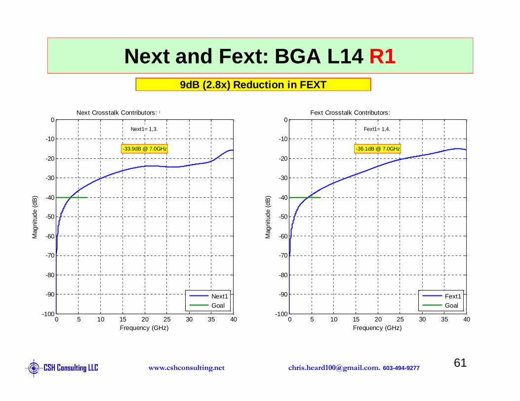
Next and Fext: BGA L14 R1
0 5 10 15 20 25 30 35 40-100
-90
-80
-70
-60
-50
-40
-30
-20
-10
0Next Crosstalk Contributors: U131 BGA L14 R1
-33.9dB @ 7.0GHz
Next1= 1,3.
Frequency (GHz)
Mag
nitu
de (
dB)
Next1Goal
0 5 10 15 20 25 30 35 40-100
-90
-80
-70
-60
-50
-40
-30
-20
-10
0Fext Crosstalk Contributors: U131 BGA L14 R1
-36.1dB @ 7.0GHz
Fext1= 1,4.
Frequency (GHz)
Mag
nitu
de (
dB)
Fext1Goal
9dB (2.8x) Reduction in FEXT
[email protected]. 603-494-9277www.cshconsulting.net 63
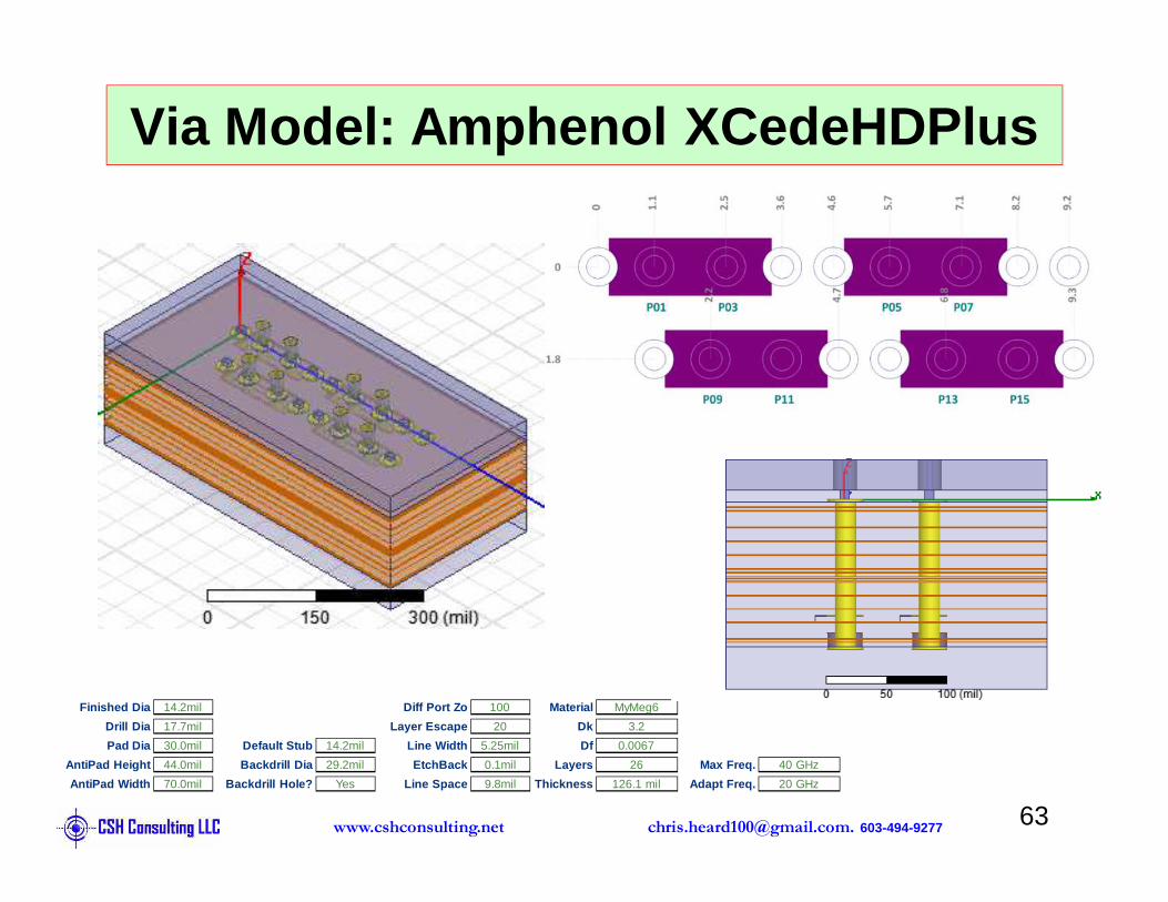
Via Model: Amphenol XCedeHDPlus
AntiPad Width 70.0mil
AntiPad Height 44.0mil
Pad Dia 30.0mil
Drill Dia 17.7mil
Finished Dia 14.2mil
Backdrill Hole? Yes
Backdrill Dia 29.2mil
Default Stub 14.2mil
Line Space 9.8mil
EtchBack 0.1mil
Line Width 5.25mil
Layer Escape 20
Diff Port Zo 100
Thickness 126.1 mil
Layers 26
Df 0.0067
Dk 3.2
Material MyMeg6
Adapt Freq. 20 GHz
Max Freq. 40 GHz
[email protected]. 603-494-9277www.cshconsulting.net 64
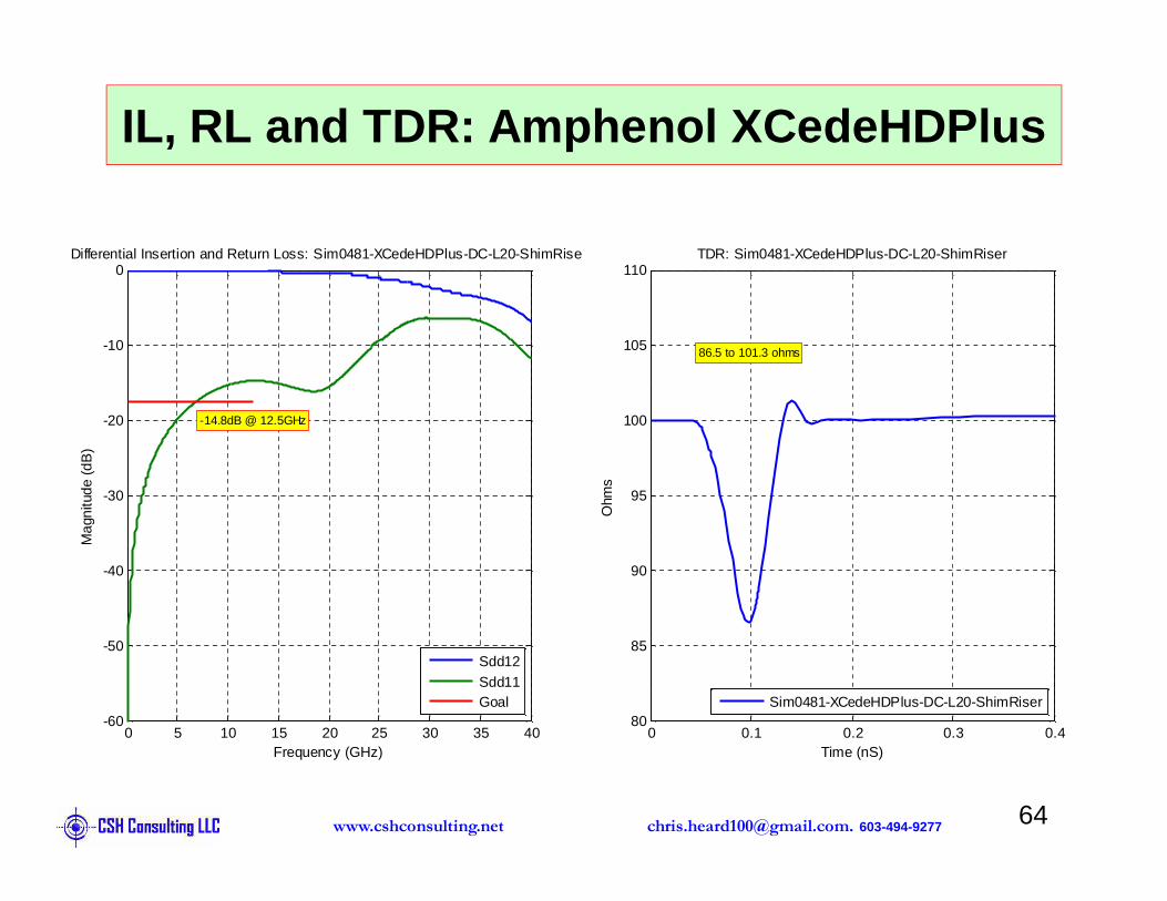
IL, RL and TDR: Amphenol XCedeHDPlus
0 5 10 15 20 25 30 35 40-60
-50
-40
-30
-20
-10
0Differential Insertion and Return Loss: Sim0481-XCedeHDPlus-DC-L20-ShimRiser
-14.8dB @ 12.5GHz
Frequency (GHz)
Mag
nitu
de (
dB)
Sdd12Sdd11Goal
0 0.1 0.2 0.3 0.480
85
90
95
100
105
110
Time (nS)
Ohm
s
86.5 to 101.3 ohms
TDR: Sim0481-XCedeHDPlus-DC-L20-ShimRiser
Sim0481-XCedeHDPlus-DC-L20-ShimRiser

[email protected]. 603-494-9277www.cshconsulting.net 65
Next and Fext: Amphenol XCedeHDPlus
0 5 10 15 20 25 30 35 40-100
-90
-80
-70
-60
-50
-40
-30
-20
-10
0Next Crosstalk Contributors: Sim0481-XCedeHDPlus-DC-L20-ShimRiser
-55.2dB @ 12.5GHz
Next1= 1,3. Next2= 1,7. Next3= 1,5. Next4= 3,5.
Frequency (GHz)
Mag
nitu
de (
dB)
Next1Next2
Next3Next4Goal
0 5 10 15 20 25 30 35 40-100
-90
-80
-70
-60
-50
-40
-30
-20
-10
0Fext Crosstalk Contributors: Sim0481-XCedeHDPlus-DC-L20-ShimRiser
-51.7dB @ 12.5GHz
Fext1= 1,4. Fext2= 1,8. Fext3= 1,6. Fext4= 3,6.
Frequency (GHz)
Mag
nitu
de (
dB)
Fext1Fext2
Fext3Fext4Goal
6.2x Lower than BGA Alternating Layer Example
[email protected]. 603-494-9277www.cshconsulting.net 66
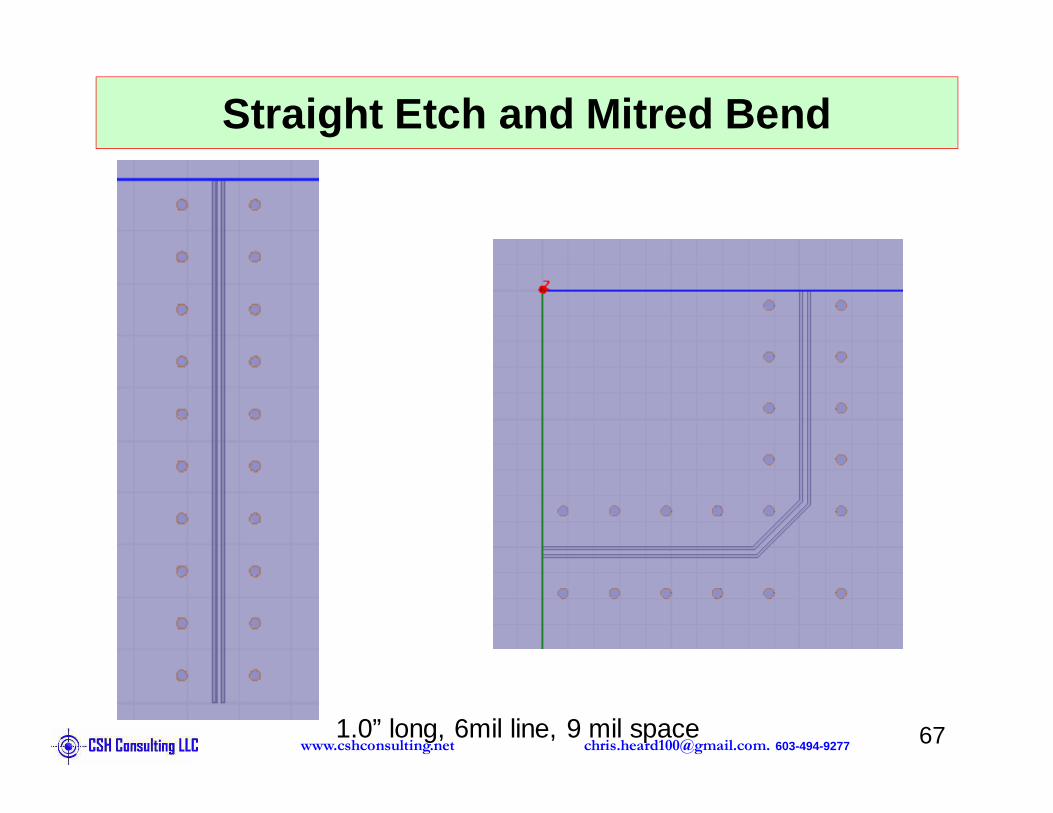
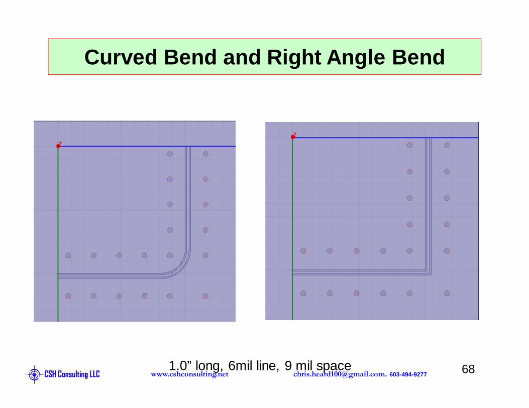
Etch Model Example: Mitre vs. Curved vs. Right Angle
[email protected]. 603-494-9277www.cshconsulting.net 67
Straight Etch and Mitred Bend
1.0” long, 6mil line, 9 mil space
[email protected]. 603-494-9277www.cshconsulting.net 68
Curved Bend and Right Angle Bend
1.0” long, 6mil line, 9 mil space
[email protected]. 603-494-9277www.cshconsulting.net
0 1 2 3 4 5 6 7 8 9 10 11 12 13 14 15 16 17 18 19 20-3
-2.75
-2.5
-2.25
-2
-1.75
-1.5
-1.25
-1
-0.75
-0.5
-0.25
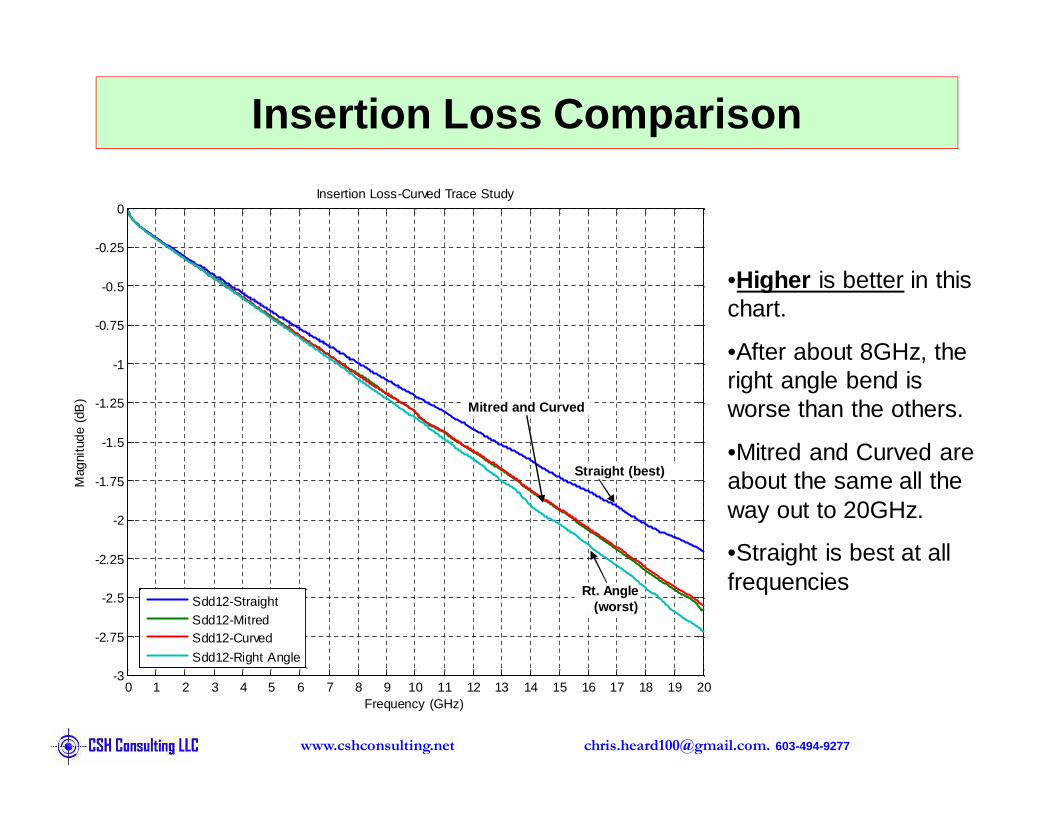
0Insertion Loss-Curved Trace Study
Frequency (GHz)
Mag
nitu
de (
dB)
Sdd12-StraightSdd12-MitredSdd12-Curved
Sdd12-Right Angle
Insertion Loss Comparison
Rt. Angle (worst)
Straight (best)
Mitred and Curved
•Higher is better in this chart.
•After about 8GHz, the right angle bend is worse than the others.
•Mitred and Curved are about the same all the way out to 20GHz.
•Straight is best at all frequencies
[email protected]. 603-494-9277www.cshconsulting.net [email protected]. 603-494-9277www.cshconsulting.net
0 1 2 3 4 5 6 7 8 9 10 11 12 13 14 15 16 17 18 19 20-40
-39
-38
-37
-36-35
-34
-33
-32
-31-30
-29
-28
-27
-26
-25-24
-23
-22
-21
-20-19
-18
-17
-16-15
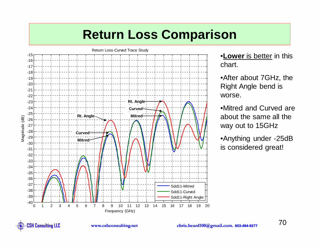
Return Loss-Curved Trace Study
Frequency (GHz)
Mag
nitu
de (
dB)
Sdd11-MitredSdd11-CurvedSdd11-Right Angle
Return Loss Comparison
Rt. Angle
Curved
Mitred
Rt. Angle
Curved
Mitred
•Lower is better in this chart.
•After about 7GHz, the Right Angle bend is worse.
•Mitred and Curved are about the same all the way out to 15GHz
•Anything under -25dB is considered great!
[email protected]. 603-494-9277www.cshconsulting.net [email protected]. 603-494-9277www.cshconsulting.net
0 0.1 0.2 0.3 0.4 0.5 0.697
98
99
100
101
102
103Time Domain Wave Form
Time (nS)
Ohm
s
Right Angle
MitredCurved
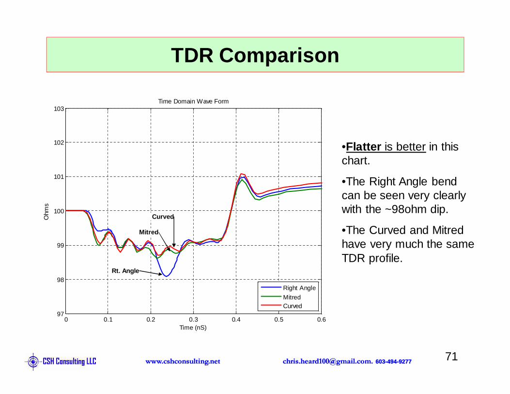
TDR Comparison
Rt. Angle
Curved
Mitred
•Flatter is better in this chart.
•The Right Angle bend can be seen very clearly with the ~98ohm dip.
•The Curved and Mitred have very much the same TDR profile.

[email protected]. 603-494-9277www.cshconsulting.net 73
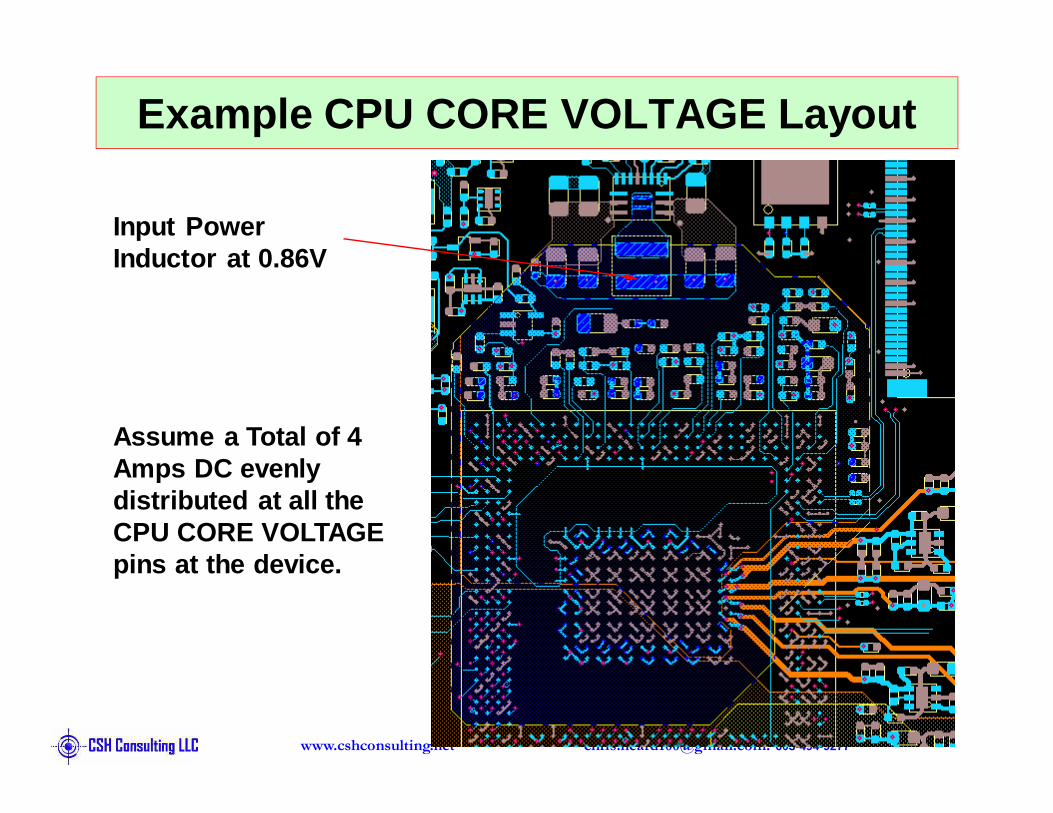
Example CPU CORE VOLTAGE Layout
Input Power Inductor at 0.86V
Assume a Total of 4 Amps DC evenly distributed at all the CPU CORE VOLTAGE pins at the device.
[email protected]. 603-494-9277www.cshconsulting.net 74
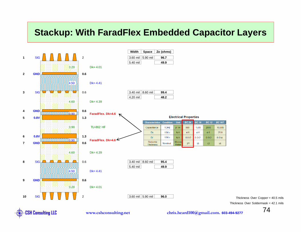
Stackup: With FaradFlex Embedded Capacitor Layers
Thickness Over Copper = 40.5 mils
Thickness Over Soldermask = 42.1 mils
1
Width Space Zo (ohms)
SIG 3.60 mil 5.90 mil 96.7
5.40 mil 49.9
2
3.20 Dk= 4.01
2 GND 0.6
4.50 Dk= 4.41
3 SIG 3.40 mil 8.60 mil 99.4
4.20 mil 48.2
0.6
4.60 Dk= 4.39
4 GND 0.60.90 FaradFlex. Dk=4.6
5 0.8V 1.3
3.90 TU-862 HF
6 0.8V 1.30.90
7 GND 0.6
4.60 Dk= 4.39
8 SIG 3.40 mil 8.60 mil 95.4
5.40 mil 49.9
0.6
4.50 Dk= 4.41
9 GND 0.6
3.20 Dk= 4.01
10 SIG 3.60 mil 5.90 mil 96.02
FaradFlex. Dk=4.6
[email protected]. 603-494-9277www.cshconsulting.net 75
Stackup: Without FaradFlex
Thickness Over Copper = 47.7 mils
Thickness Over Soldermask = 49.3 mils
1
Width Space Zo (ohms)
SIG 3.60 mil 5.90 mil 96.7
5.40 mil 49.9
2
3.20 Dk= 4.01
2 GND 0.6
4.50 Dk= 4.41
3 SIG 3.40 mil 8.60 mil 99.4
4.20 mil 48.2
0.6
4.60 Dk= 4.39
4 GND 0.6
4.50 Dk= 4.39
5 0.8V 1.3
3.90 TU-862 HF
6 0.8V 1.3
4.50 Dk= 4.39
7 GND 0.6
4.60 Dk= 4.39
8 SIG 3.40 mil 8.60 mil 95.4
5.40 mil 49.9
0.6
4.50 Dk= 4.41
9 GND 0.6
3.20 Dk= 4.01
10 SIG 3.60 mil 5.90 mil 96.02
[email protected]. 603-494-9277www.cshconsulting.net 76
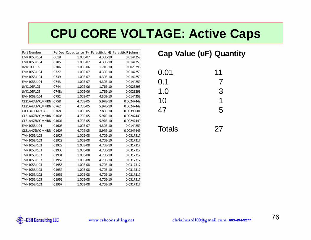
CPU CORE VOLTAGE: Active CapsCap Value (uF) Quantity
0.01 110.1 71.0 310 147 5
Totals 27
Part Number RefDes Capacitance (F) Parasitic L (H) Parasitic R (ohms)
EMK105BJ104 C618 1.00E-07 4.30E-10 0.0144259
EMK105BJ104 C705 1.00E-07 4.30E-10 0.0144259
JMK105F105 C706 1.00E-06 1.71E-10 0.0023298
EMK105BJ104 C727 1.00E-07 4.30E-10 0.0144259
EMK105BJ104 C739 1.00E-07 4.30E-10 0.0144259
EMK105BJ104 C743 1.00E-07 4.30E-10 0.0144259
JMK105F105 C744 1.00E-06 1.71E-10 0.0023298
JMK105F105 C748a 1.00E-06 1.71E-10 0.0023298
EMK105BJ104 C752 1.00E-07 4.30E-10 0.0144259
CL21A476MQMNRN C758 4.70E-05 5.97E-10 0.00247449
CL21A476MQMNRN C762 4.70E-05 5.97E-10 0.00247449
C0603C106K9PAC C768 1.00E-05 7.86E-10 0.00390001
CL21A476MQMNRN C1603 4.70E-05 5.97E-10 0.00247449
CL21A476MQMNRN C1604 4.70E-05 5.97E-10 0.00247449
EMK105BJ104 C1606 1.00E-07 4.30E-10 0.0144259
CL21A476MQMNRN C1607 4.70E-05 5.97E-10 0.00247449
TMK105BJ103 C1927 1.00E-08 4.70E-10 0.0317317
TMK105BJ103 C1928 1.00E-08 4.70E-10 0.0317317
TMK105BJ103 C1929 1.00E-08 4.70E-10 0.0317317
TMK105BJ103 C1930 1.00E-08 4.70E-10 0.0317317
TMK105BJ103 C1931 1.00E-08 4.70E-10 0.0317317
TMK105BJ103 C1952 1.00E-08 4.70E-10 0.0317317
TMK105BJ103 C1953 1.00E-08 4.70E-10 0.0317317
TMK105BJ103 C1954 1.00E-08 4.70E-10 0.0317317
TMK105BJ103 C1955 1.00E-08 4.70E-10 0.0317317
TMK105BJ103 C1956 1.00E-08 4.70E-10 0.0317317
TMK105BJ103 C1957 1.00E-08 4.70E-10 0.0317317

[email protected]. 603-494-9277www.cshconsulting.net 77
CPU CORE VOLTAGE Plane SI Wave Import
IC200 Port
Current Sinks& Caps
Voltage Source (0.86v,
0.001ohm) & Caps
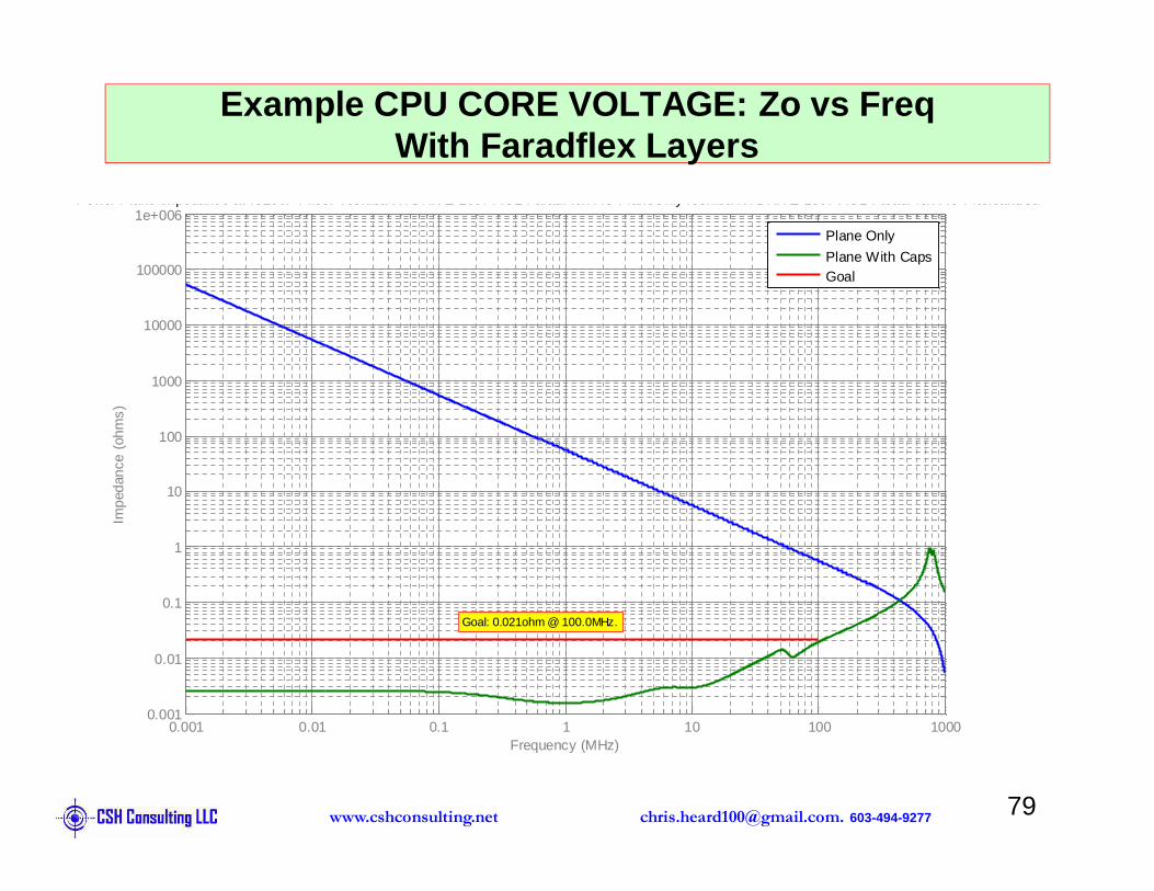
[email protected]. 603-494-9277www.cshconsulting.net 79
0.001 0.01 0.1 1 10 100 10000.001
0.01
0.1
1
10
100
1000
10000
100000
1e+006
Frequency (MHz)
Impe
danc
e (o
hms)
Power Plane Impedance at IC200. Files: Toshiba KVDRIVE 1007 AO1 FaradFlex AC PlaneOnlyToshiba KVDRIVE 1007 AO1 FaradFlex AC PlaneandCaps
Goal: 0.021ohm @ 100.0MHz.
Plane Only
Plane With CapsGoal
Example CPU CORE VOLTAGE: Zo vs Freq With Faradflex Layers
[email protected]. 603-494-9277www.cshconsulting.net 80
0.001 0.01 0.1 1 10 100 10000.001
0.01
0.1
1
10
100
1000
10000
100000
1e+006
Frequency (MHz)
Impe
danc
e (o
hms)
Goal: 0.021ohm @ 100.0MHz.
Plane Only
Plane With CapsGoal
Example CPU CORE VOLTAGE: Zo vs Freq With Faradflex Layers and No 0.01uF Caps
[email protected]. 603-494-9277www.cshconsulting.net 81
0.001 0.01 0.1 1 10 100 10000.001
0.01
0.1
1
10
100
1000
10000
100000
1e+006
Frequency (MHz)
Impe
danc
e (o
hms)
Goal: 0.021ohm @ 100.0MHz.
Plane Only
Plane With CapsGoal
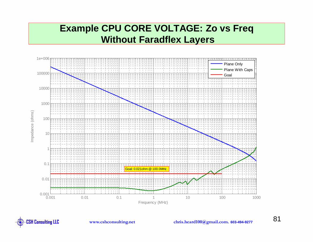
Example CPU CORE VOLTAGE: Zo vs Freq Without Faradflex Layers

[email protected]. 603-494-9277www.cshconsulting.net 83
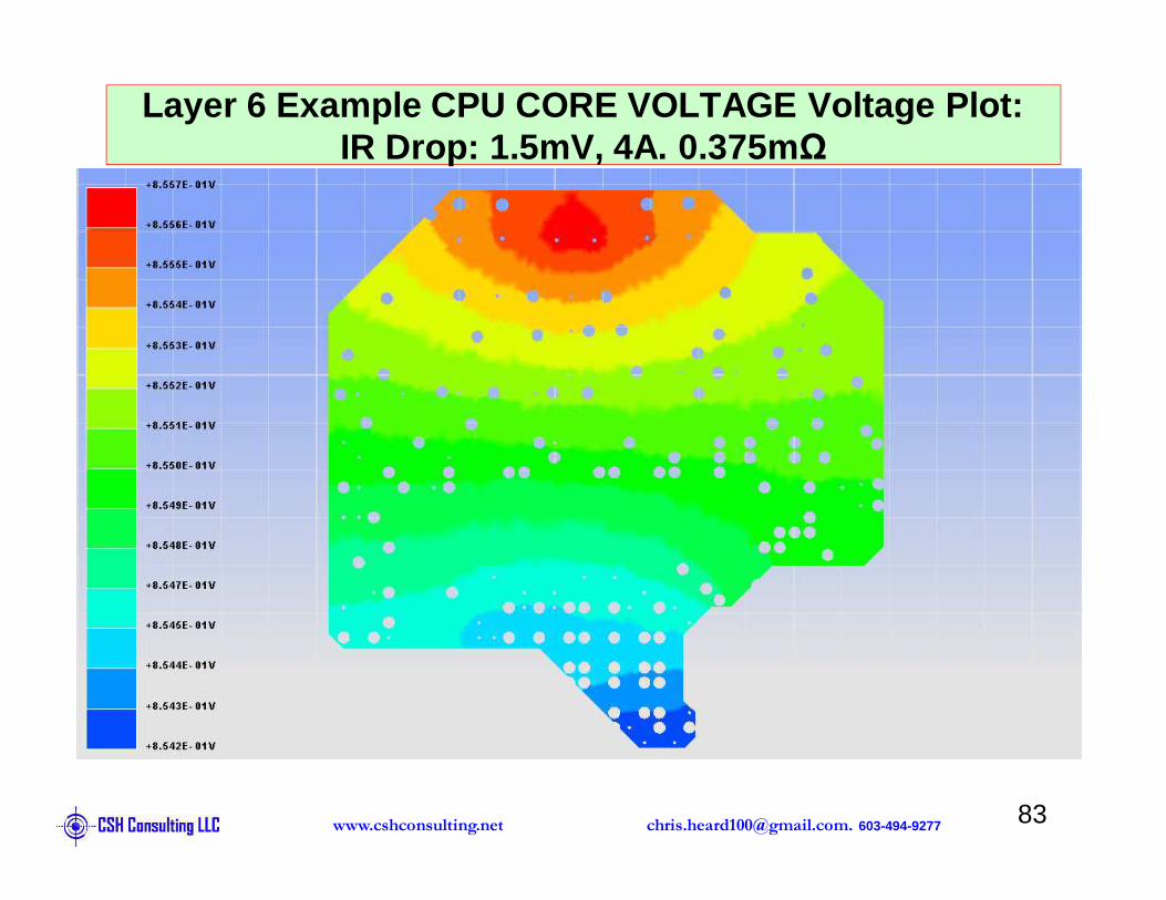
Layer 6 Example CPU CORE VOLTAGE Voltage Plot:IR Drop: 1.5mV, 4A. 0.375m Ω
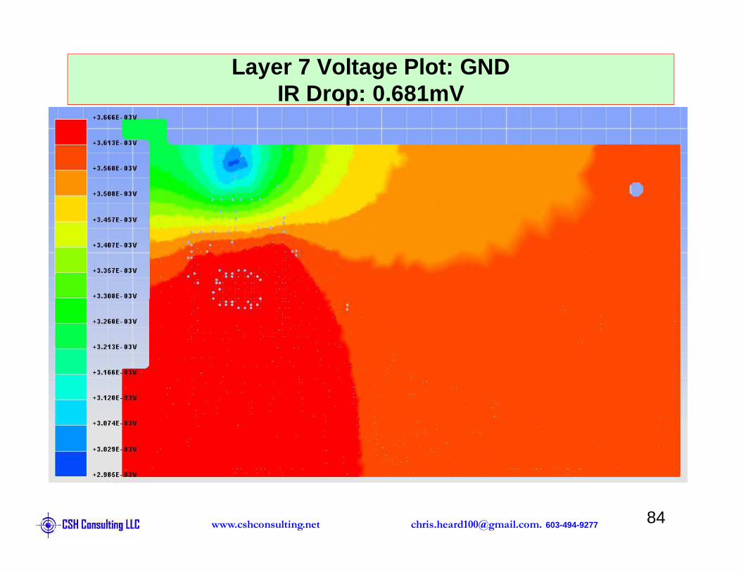

[email protected]. 603-494-9277www.cshconsulting.net [email protected]. 603-494-9277www.cshconsulting.net
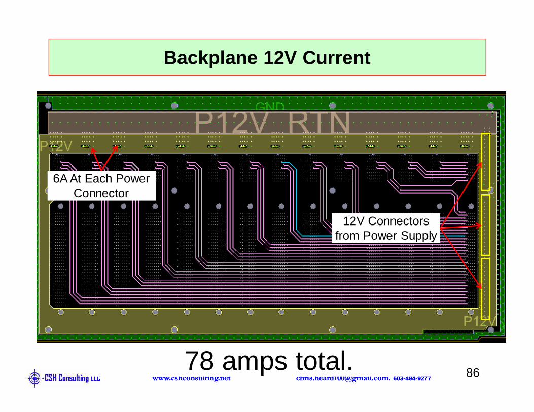
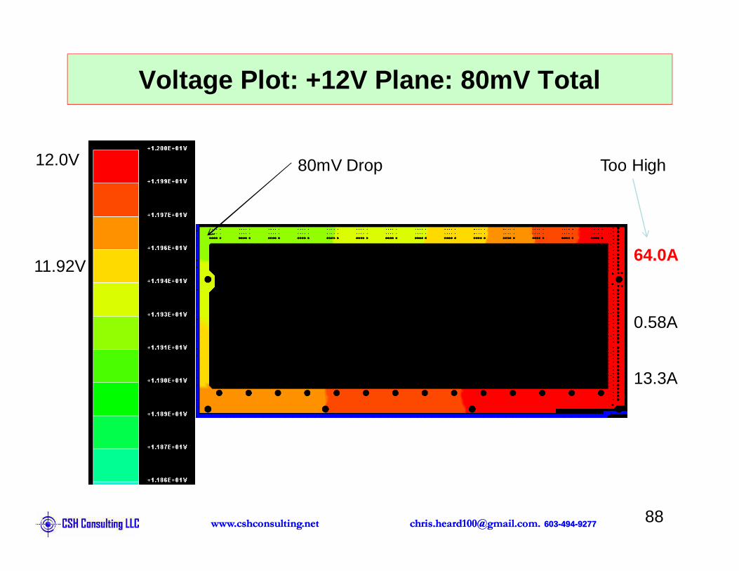
78 amps total.
Backplane 12V Current
6A At Each Power Connector
12V Connectors from Power Supply
[email protected]. 603-494-9277www.cshconsulting.net 87
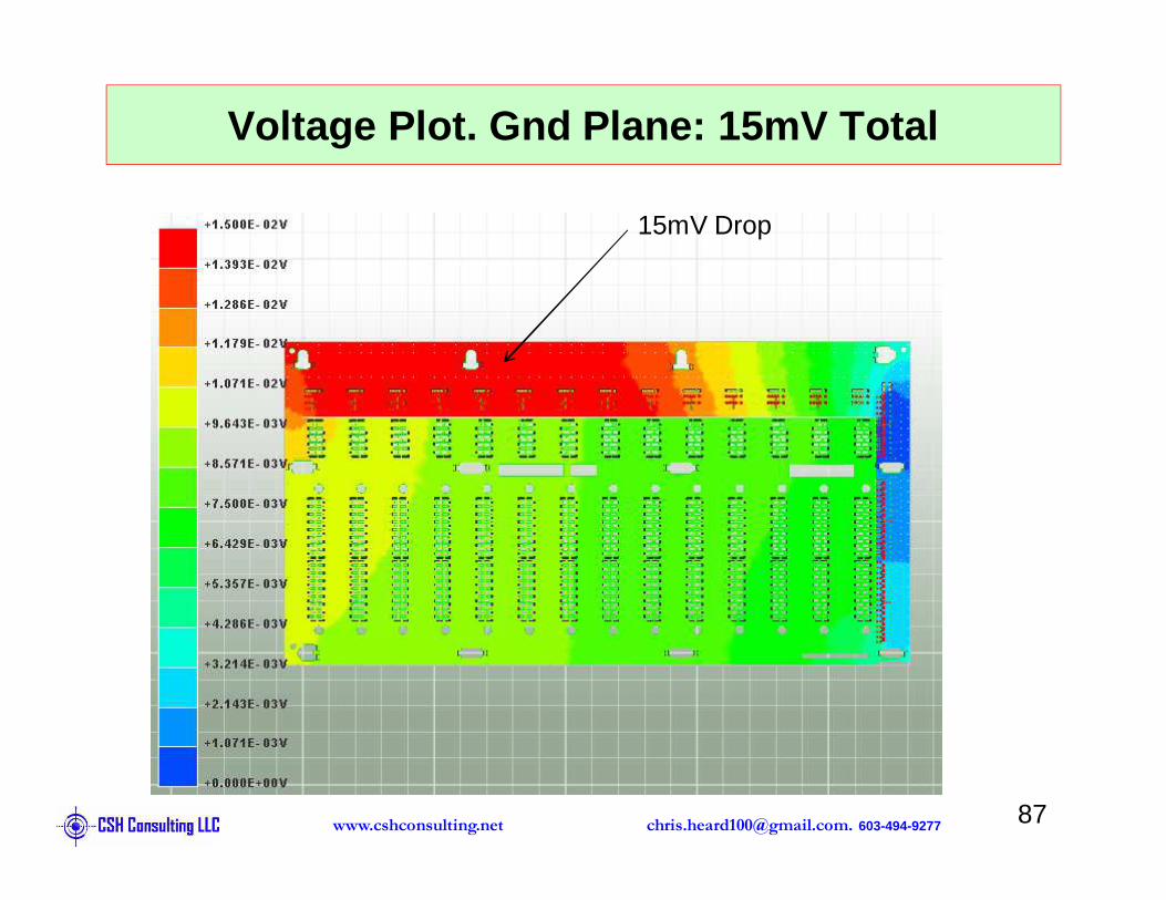
Voltage Plot. Gnd Plane: 15mV Total
15mV Drop
[email protected]. 603-494-9277www.cshconsulting.net [email protected]. 603-494-9277www.cshconsulting.net
Voltage Plot: +12V Plane: 80mV Total
80mV Drop
64.0A
0.58A
13.3A
12.0V
11.92V
Too High
[email protected]. 603-494-9277www.cshconsulting.net [email protected]. 603-494-9277www.cshconsulting.net
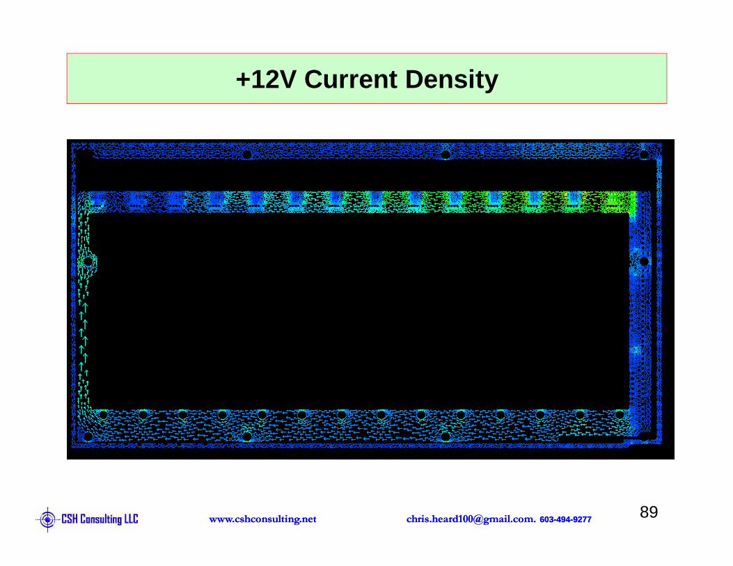
+12V Current Density