pcb trace impedance: impact of localized pcb copper density · plane on the layer 4 outerlayer....
TRANSCRIPT

PCB Trace Impedance: Impact of Localized PCB Copper Density
Gary A. Brist, Jeff Krieger, Dan Willis
Intel Corp
Hillsboro, OR
Abstract
Trace impedances are specified and controlled on PCBs as their nominal impedance value and variations are key factors in establishing
system I/O bus performance. PCB trace impedances are evaluated and controlled during manufacturing using impedance coupon
structures. An issue critical to many high performance I/O busses is that the actual bus impedance is shifted and the intra-bus variation
is larger than measured using the impedance coupons, leading to PCB motherboards being Out of Specification. Recent work has
shown that shifts in measured impedances across a PCB layer is correlated to localized changes in copper density within the PCB fabrication panel due to both the motherboard design and the PCB manufacture’s selection of fill pattern and impedance coupon
location. Managing the copper density across the fabrication panel through proper coupon design, placement, and copper fill pattern
selection is required to minimize impedance shifts between coupons and product. This paper highlights the impact of copper density on
PCB trace impedances and provides a BKM (Best Known Method) for managing copper density and designing impedance coupons to
minimize impedance shifts and variations that otherwise could lead to Out of Specification impedances on PCB motherboards.
Introduction
Copper density and copper density transitions drive changes in trace impedance by altering the dielectric thickness and electrical
properties of traces. The impact of copper density transitions have also been shown to extend to adjacent layers of the PCB. As a
result, localized copper density and copper density transitions must be managed within both the design and the fabrication panel.
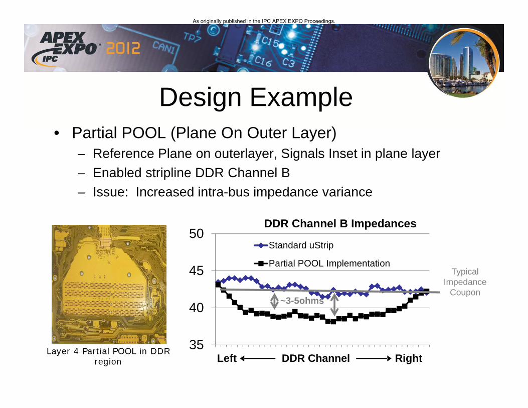
Recent desktop designs implemented a Partial POOL (Planes On Outer Layer) structure on the PCB motherboard for DDR bus Channel B to improve signal margins at equivalent bus lengths and routing rules. The Partial POOL structure as
implemented in a four layer PCB inset the DDR channel B routing into the Layer 3 plane and placed the DDR reference
plane on the Layer 4 outerlayer. This resulted in a localized region of low copper density on Layer 3. During the test board
builds, two issues were discovered within the Partial POOL DDR implementation. First, the trace impedances near the center
of the Partial POOL DDR region were notably lower than impedances at edge of the region as shown in Figure 1. Secondly,
a significant impedance offset was observed between the impedance coupons used by fabricators to select line widths and the
impedance values across the DDR Channels.
Figure Error! No text of specified style in document. - Intra-channel Impedance Variation across Multiple
Motherboards
Measured impedance of DDR data signals at the center of the Partial POOL DDR Channel B extended ~3-5 ohms lower than measured
DDR data signal impedances at edge of the routing channel. The measured decrease was significant in that the 3-5ohm increase in
intra-bus variation consumed roughly 50% of the allowable impedance tolerance for 40ohm +/-15% DDR signals. The measured
change in variation exceeded the modeled intra-bus variation and required Signal Integrity engineers to update simulation models for
the DDR channels. Conversely, measured impedances within the Layer 1 microstrip DDR Channel A generally followed trends
measured on previous platform builds and had both low intra channel impedance range and expected board to board variation.
Investigation across multiple OEM motherboards that implemented Partial POOL as well as internally purchased PCBs built at
different fabricators with various materials showed that all designs which implemented Partial POOL had a similar impedance profile
+5
0
– 5
+5
0
– 5
Ohms
Ohms
Standard uStrip
Partial POOL
Transition Center of Void Transition Region Region
Hi Z MB :
Hi Z MB :
Low Z MB
+5
0
– 5
+5
0
– 5
Standard (Layer 1)
Partial POOL (Layer 3)
Left DDR Channel Right
Transition Center of Void Transition Region Region
Hi Z MB :
Low Z MB
Hi Z MB :
Low Z MB
Coupon Impedances
Microstrip traces
Partial POOL traces
As originally published in the IPC APEX EXPO Proceedings.

within the Partial POOL region. Final analysis showed that copper density variations within the PCB fabrication panel corresponded to
changes in the dielectric thickness profile across the Partial POOL region and thus altered impedances.
Secondly, Impedance offset between the impedance coupon and the DDR channel induced an impedance shift as fabricators controlled
the line widths based on measurements from their standard coupon layouts. Figure 1 shows the measured impedances across the DDR
regions with the manufacturing coupons impedances for each panel highlighted by the rectangle on right of each impedance plot. The coupon impedances for Partial POOL DDR were closely matched to the impedances at the edge of the Partial POOL DDR region; but,
there was a marked offset to impedances at Center of Void. The Center of Void offset was of special concern as the DDR address,
control, clock and command traces were fully located at center of DDR region and were thus shifted toward the low impedance corner
with some individual traces out of specification. In addition, the impedances within Layer 1 microstrip DDR regions were also shifted
and measured slightly higher than the coupon. The differences between the impedance coupon and the DDR channel was found to
result from variations in the copper density across the manufacturing panel due to the motherboard layout, impedance coupon location
and design, and the fill pattern selected by PCB fabricator. During analysis, it was discovered that a high to low copper density
transition within the Layer 3 Partial POOL DDR region correlated to an increase in the nominal dielectric thickness between Layer 1
and Layer 2, resulting in the increased Layer 1 microstrip DDR bus impedance.
The result of the Partial POOL DDR implementation highlighted the impact of copper density variations on PCB dielectric thicknesses
and impedances. Signal Integrity Engineers need to evaluate designs for copper density variations and may need to account for higher variations in modeling and simulations. It was also found that local copper density variations on a single layer affect the impedances
and dielectric thicknesses on multiple layers. While the correlation between copper density and dielectric thickness variations can be
incorporated into electrical simulations, it is very important that proper design and procurement methods are followed to minimize
inherent impedance offsets within procured motherboards.
Copper Density Impact on Local Trace Embedding
The Partial POOL structure, as implemented in a four layer motherboard, utilized a portion of the Layer 3 PCB plane for
DDR memory signal routing as shown in Figure 2, and placed the reference plane for these signals on the Layer 4 external
PCB layer as shown in Figure 3. Layer 2 was a plane and Layer 1 used for signaling. The PCB core and prepreg material
selection for the Partial POOL design was the same as a traditional four layer microstrip PCB design which consisted of 1080
prepreg between Layer 1 and Layer 2, 49mil core between Layer 2 and Layer 3, and 1080 prepreg between Layer 3 and Layer 4. This maintained desired z-axis symmetry and uniform dielectric thicknesses for all microstrip IO interfaces in both
the traditional microstrip design and Partial POOL implementation.
Trace embedding within the Partial POOL region results from the redistribution of prepreg material around lower copper density signal
traces during lamination at high pressure and elevated temperature. In typical glass reinforced PCB dielectrics, local changes in
thickness correspond to changes in its glass to resin ratio which influence the localized dielectric properties. In traditional Layer 4
microstrip routing, the dielectric thickness between the Layer 4 signals and the Layer 3 reference plane is fairly consistent across the
DDR region. During the lamination process, the Layer 3 reference plane of a traditional design has a high copper density which is
uniform across the entire image and the Layer 4 copper is an un-etched copper layer. As a result, the prepreg dielectric between Layer 4
and Layer 3 is essentially laminated between two solid copper planes providing a uniform dielectric thickness for traditional Layer 4
microstrip routing. However, within a Partial POOL design Layer 3 has a high copper density except within the DDR routing region
where the copper density drops significantly. During lamination, the dielectric core of the PCB bends and the prepreg epoxy materials move to fill the void created by the low copper density, altering the dielectric thickness within the DDR region. The implementation of
Partial in the DDR subsection highlighted the dielectric and impedance impacts of copper density.
Figure 2 - Representative Layer 3 Artwork for DDR Partial POOL
Traces Typical Zo
Data/Cntrl 40 ohm
CMD/ADDR 32 ohm
CLK 62 ohm
As originally published in the IPC APEX EXPO Proceedings.
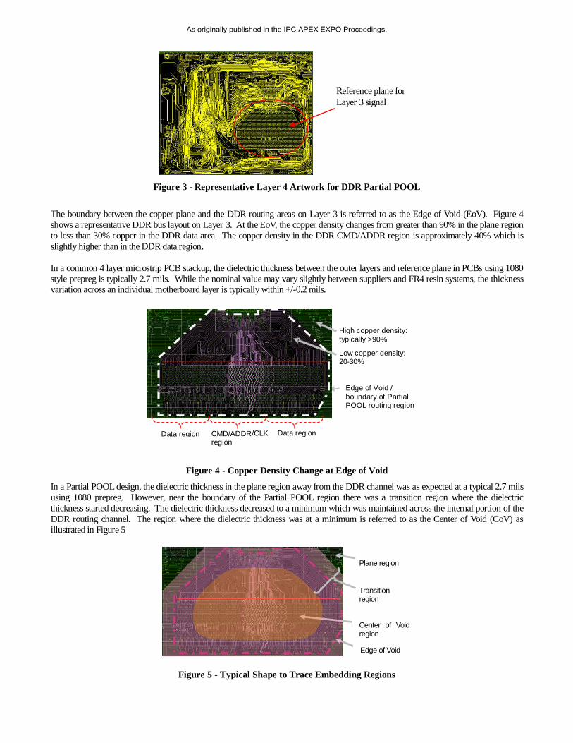
Figure 3 - Representative Layer 4 Artwork for DDR Partial POOL
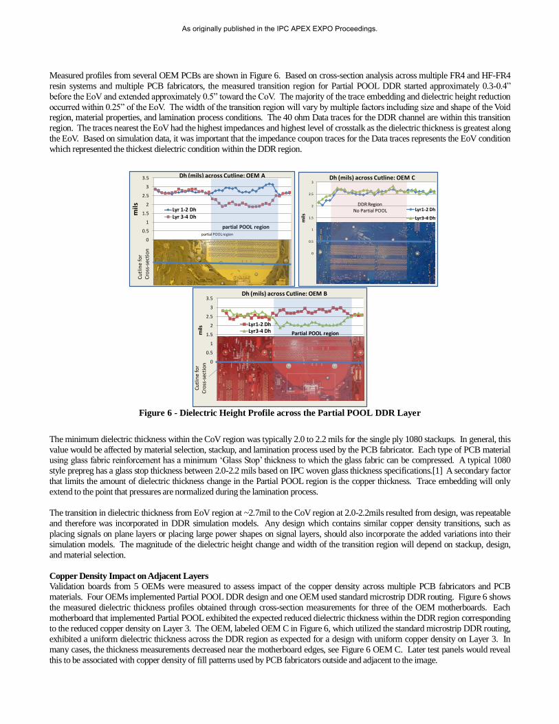
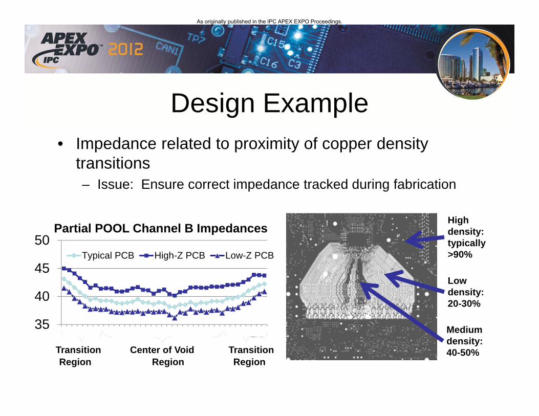
The boundary between the copper plane and the DDR routing areas on Layer 3 is referred to as the Edge of Void (EoV). Figure 4
shows a representative DDR bus layout on Layer 3. At the EoV, the copper density changes from greater than 90% in the plane region
to less than 30% copper in the DDR data area. The copper density in the DDR CMD/ADDR region is approximately 40% which is
slightly higher than in the DDR data region.
In a common 4 layer microstrip PCB stackup, the dielectric thickness between the outer layers and reference plane in PCBs using 1080
style prepreg is typically 2.7 mils. While the nominal value may vary slightly between suppliers and FR4 resin systems, the thickness variation across an individual motherboard layer is typically within +/-0.2 mils.
Figure 4 - Copper Density Change at Edge of Void
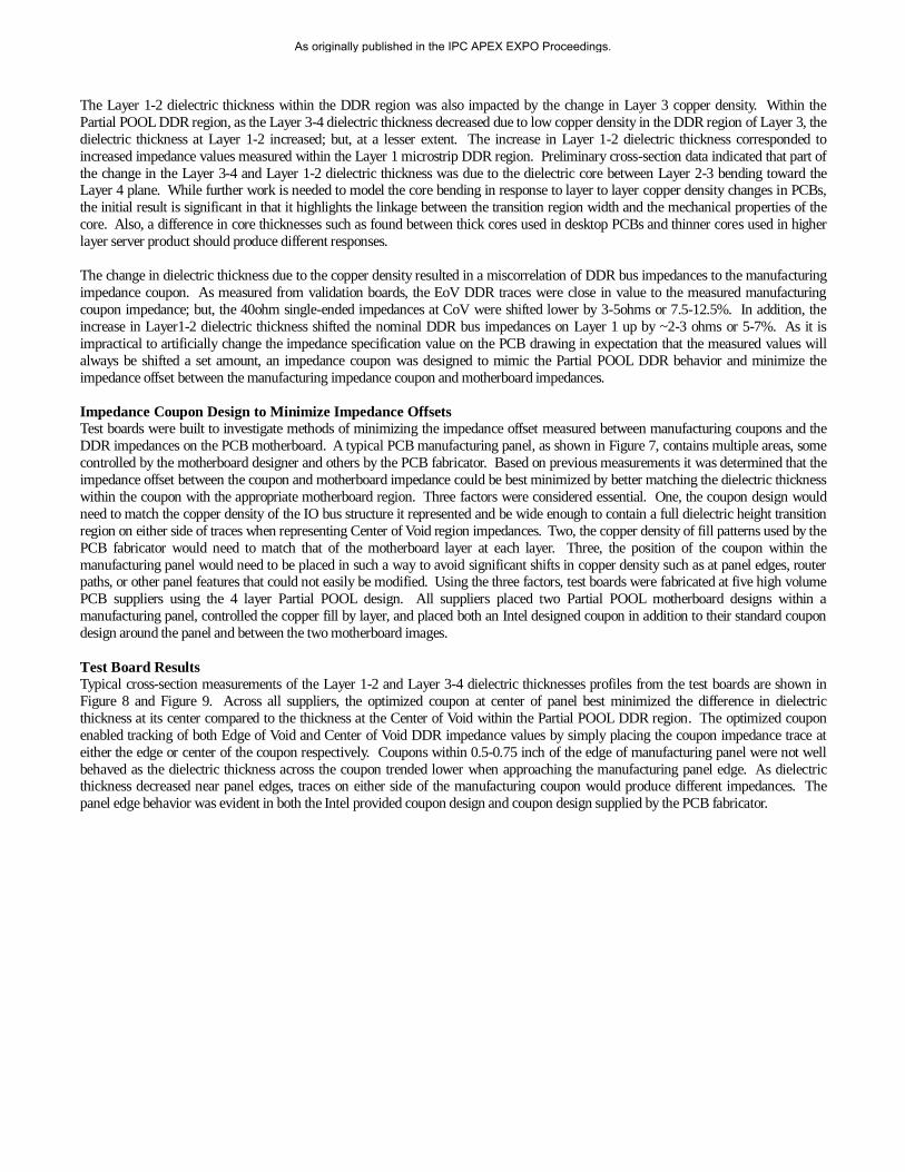
In a Partial POOL design, the dielectric thickness in the plane region away from the DDR channel was as expected at a typical 2.7 mils
using 1080 prepreg. However, near the boundary of the Partial POOL region there was a transition region where the dielectric
thickness started decreasing. The dielectric thickness decreased to a minimum which was maintained across the internal portion of the
DDR routing channel. The region where the dielectric thickness was at a minimum is referred to as the Center of Void (CoV) as
illustrated in Figure 5
Center of Void region
Plane region
Transition region
Edge of Void
Figure 5 - Typical Shape to Trace Embedding Regions
CMD/ADDR /CLK region
Data region Data region
High copper density: typically >90%
Low copper density: 20 - 30%
Edge of Void / boundary of Partial POOL routing region
Reference plane for
Layer 3 signal
As originally published in the IPC APEX EXPO Proceedings.
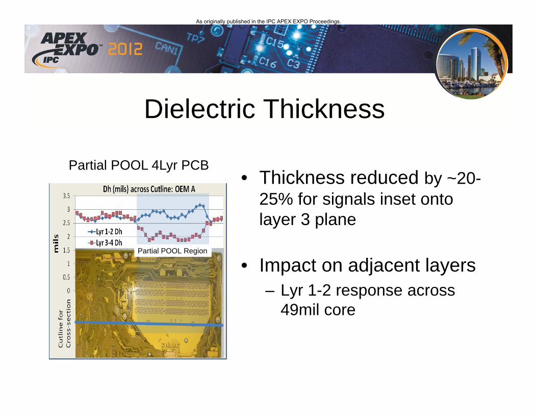
Measured profiles from several OEM PCBs are shown in Figure 6. Based on cross-section analysis across multiple FR4 and HF-FR4
resin systems and multiple PCB fabricators, the measured transition region for Partial POOL DDR started approximately 0.3-0.4”
before the EoV and extended approximately 0.5” toward the CoV. The majority of the trace embedding and dielectric height reduction
occurred within 0.25” of the EoV. The width of the transition region will vary by multiple factors including size and shape of the Void region, material properties, and lamination process conditions. The 40 ohm Data traces for the DDR channel are within this transition
region. The traces nearest the EoV had the highest impedances and highest level of crosstalk as the dielectric thickness is greatest along
the EoV. Based on simulation data, it was important that the impedance coupon traces for the Data traces represents the EoV condition
which represented the thickest dielectric condition within the DDR region.
Cu
tlin
e fo
r C
ross
-sec
tio
n
Dh (mils) across Cutline: OEM A
0
0.5
1
1.5
2
2.5
3
3.5
mil
s
Lyr 1-2 DhLyr 3-4 Dh
partial POOL region
partial POOL region
0
0.5
1
1.5
2
2.5
3
mil
s
Lyr1-2 Dh
Lyr3-4 Dh
Dh (mils) across Cutline: OEM C
DDR RegionNo Partial POOL
0
0.5
1
1.5
2
2.5
3
3.5
mils
Lyr1-2 DhLyr3-4 Dh
Cu
tlin
e fo
r C
ross
-sec
tio
n
Partial POOL region
Dh (mils) across Cutline: OEM B
Figure 6 - Dielectric Height Profile across the Partial POOL DDR Layer
The minimum dielectric thickness within the CoV region was typically 2.0 to 2.2 mils for the single ply 1080 stackups. In general, this
value would be affected by material selection, stackup, and lamination process used by the PCB fabricator. Each type of PCB material using glass fabric reinforcement has a minimum ‘Glass Stop’ thickness to which the glass fabric can be compressed. A typical 1080
style prepreg has a glass stop thickness between 2.0-2.2 mils based on IPC woven glass thickness specifications.[1] A secondary factor
that limits the amount of dielectric thickness change in the Partial POOL region is the copper thickness. Trace embedding will only
extend to the point that pressures are normalized during the lamination process.
The transition in dielectric thickness from EoV region at ~2.7mil to the CoV region at 2.0-2.2mils resulted from design, was repeatable
and therefore was incorporated in DDR simulation models. Any design which contains similar copper density transitions, such as
placing signals on plane layers or placing large power shapes on signal layers, should also incorporate the added variations into their
simulation models. The magnitude of the dielectric height change and width of the transition region will depend on stackup, design,
and material selection.
Copper Density Impact on Adjacent Layers
Validation boards from 5 OEMs were measured to assess impact of the copper density across multiple PCB fabricators and PCB
materials. Four OEMs implemented Partial POOL DDR design and one OEM used standard microstrip DDR routing. Figure 6 shows
the measured dielectric thickness profiles obtained through cross-section measurements for three of the OEM motherboards. Each
motherboard that implemented Partial POOL exhibited the expected reduced dielectric thickness within the DDR region corresponding
to the reduced copper density on Layer 3. The OEM, labeled OEM C in Figure 6, which utilized the standard microstrip DDR routing,
exhibited a uniform dielectric thickness across the DDR region as expected for a design with uniform copper density on Layer 3. In
many cases, the thickness measurements decreased near the motherboard edges, see Figure 6 OEM C. Later test panels would reveal
this to be associated with copper density of fill patterns used by PCB fabricators outside and adjacent to the image.
As originally published in the IPC APEX EXPO Proceedings.
The Layer 1-2 dielectric thickness within the DDR region was also impacted by the change in Layer 3 copper density. Within the
Partial POOL DDR region, as the Layer 3-4 dielectric thickness decreased due to low copper density in the DDR region of Layer 3, the
dielectric thickness at Layer 1-2 increased; but, at a lesser extent. The increase in Layer 1-2 dielectric thickness corresponded to
increased impedance values measured within the Layer 1 microstrip DDR region. Preliminary cross-section data indicated that part of
the change in the Layer 3-4 and Layer 1-2 dielectric thickness was due to the dielectric core between Layer 2-3 bending toward the Layer 4 plane. While further work is needed to model the core bending in response to layer to layer copper density changes in PCBs,
the initial result is significant in that it highlights the linkage between the transition region width and the mechanical properties of the
core. Also, a difference in core thicknesses such as found between thick cores used in desktop PCBs and thinner cores used in higher
layer server product should produce different responses.
The change in dielectric thickness due to the copper density resulted in a miscorrelation of DDR bus impedances to the manufacturing
impedance coupon. As measured from validation boards, the EoV DDR traces were close in value to the measured manufacturing
coupon impedance; but, the 40ohm single-ended impedances at CoV were shifted lower by 3-5ohms or 7.5-12.5%. In addition, the
increase in Layer1-2 dielectric thickness shifted the nominal DDR bus impedances on Layer 1 up by ~2-3 ohms or 5-7%. As it is
impractical to artificially change the impedance specification value on the PCB drawing in expectation that the measured values will
always be shifted a set amount, an impedance coupon was designed to mimic the Partial POOL DDR behavior and minimize the
impedance offset between the manufacturing impedance coupon and motherboard impedances.
Impedance Coupon Design to Minimize Impedance Offsets
Test boards were built to investigate methods of minimizing the impedance offset measured between manufacturing coupons and the
DDR impedances on the PCB motherboard. A typical PCB manufacturing panel, as shown in Figure 7, contains multiple areas, some
controlled by the motherboard designer and others by the PCB fabricator. Based on previous measurements it was determined that the
impedance offset between the coupon and motherboard impedance could be best minimized by better matching the dielectric thickness
within the coupon with the appropriate motherboard region. Three factors were considered essential. One, the coupon design would
need to match the copper density of the IO bus structure it represented and be wide enough to contain a full dielectric height transition
region on either side of traces when representing Center of Void region impedances. Two, the copper density of fill patterns used by the
PCB fabricator would need to match that of the motherboard layer at each layer. Three, the position of the coupon within the
manufacturing panel would need to be placed in such a way to avoid significant shifts in copper density such as at panel edges, router paths, or other panel features that could not easily be modified. Using the three factors, test boards were fabricated at five high volume
PCB suppliers using the 4 layer Partial POOL design. All suppliers placed two Partial POOL motherboard designs within a
manufacturing panel, controlled the copper fill by layer, and placed both an Intel designed coupon in addition to their standard coupon
design around the panel and between the two motherboard images.
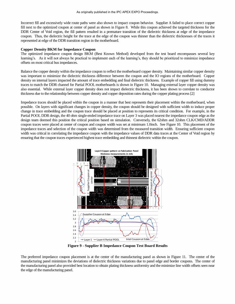
Test Board Results
Typical cross-section measurements of the Layer 1-2 and Layer 3-4 dielectric thicknesses profiles from the test boards are shown in
Figure 8 and Figure 9. Across all suppliers, the optimized coupon at center of panel best minimized the difference in dielectric
thickness at its center compared to the thickness at the Center of Void within the Partial POOL DDR region. The optimized coupon
enabled tracking of both Edge of Void and Center of Void DDR impedance values by simply placing the coupon impedance trace at
either the edge or center of the coupon respectively. Coupons within 0.5-0.75 inch of the edge of manufacturing panel were not well
behaved as the dielectric thickness across the coupon trended lower when approaching the manufacturing panel edge. As dielectric thickness decreased near panel edges, traces on either side of the manufacturing coupon would produce different impedances. The
panel edge behavior was evident in both the Intel provided coupon design and coupon design supplied by the PCB fabricator.
As originally published in the IPC APEX EXPO Proceedings.
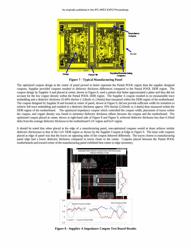
Figure 7 - Typical Manufacturing Panel
The optimized coupon design at the center of panel proved to better represent the Partial POOL region than the supplier designed
coupons. Supplier provided coupons resulted in dielectric thickness differences compared to the Partial POOL DDR region. The
coupon design by Supplier A and placed at center, shown in Figure 8, used a pattern that better approximated a plane and thus did not account for the low copper density within the Partial POOL DDR region. The Supplier A coupon resulted in no measureable trace
embedding and a dielectric thickness 35-40% thicker (~2.8mils vs 2.0mils) than measured within the DDR region of the motherboard.
The coupon designed by Supplier B and located at center of panel, shown in Figure 9, did not provide sufficient width for transition to
achieve full trace embedding and resulted in a dielectric thickness approx 10% thicker (2.65mils vs 2.4mils) than measured within the
DDR region of the motherboard. The optimized impedance coupon which controlled the coupon width, placement of traces within
the coupon, and copper density was found to minimize dielectric thickness offsets between the coupon and the motherboard. The
optimized coupon placed at center, shown at right-hand side of Figure 8 and Figure 9, achieved dielectric thickness less than 0.10mil
delta from the average dielectric thickness in the motherboard CoV region and EoV region.
It should be noted that when placed at the edge of a manufacturing panel, non-optimized coupons would at times achieve similar
dielectric thicknesses to that of the CoV DDR region as shown by the Supplier Coupon at Edge in Figure 9. The issue with coupons
placed at edge of panel was that the traces on opposing sides of the coupon behaved differently. The traces closest to manufacturing panel edge had a lower dielectric thickness compared to traces closer to the center. Coupons placed between the Partial POOL
motherboards and toward center of the manufacturing panel exhibited best center to edge symmetry.
0
0.51
1.52
2.53
3.5
12
34
56
78
91
01
11
21
31
41
51
61
71
81
92
0
Seri
es1
Seri
es2
1.5
2
2.5
3
3.5
Layer 1 Layer 4 Partial POOL
00.511.522.53
12
34
56
78
910
1112
1314
1516
1718
1920
2122
2324
2526
2728
2930
3132
3334
3536
3738
3940
41
Serie
s2
Serie
s3
Fabrication Panel thickness measurements from Cross-sectionDielectric Thickness in mils
Intel Coupon at EdgeSupplier Coupon at Edge
Sup
plie
r Co
up
on
at
cen
ter
Inte
l Co
up
on
at
cen
ter
Figure 8 - Supplier A Impedance Coupon Test Board Results
As originally published in the IPC APEX EXPO Proceedings.
Incorrect fill and excessively wide route paths were also shown to impact coupon behavior. Supplier A failed to place correct copper
fill next to the optimized coupon at center of panel as shown in Figure 8. While this coupon achieved the targeted thickness for the
DDR Center of Void region, the fill pattern resulted in a premature transition of the dielectric thickness at edge of the impedance
coupon. Thus, the dielectric height for the trace at the edge of the coupon was thinner than the dielectric thicknesses of the traces it
represented at edge of the DDR transition region in the motherboard.
Copper Density BKM for Impedance Coupon
The optimized impedance coupon design BKM (Best Known Method) developed from the test board encompasses several key
learning’s. As it will not always be practical to implement each of the learning’s, they should be prioritized to minimize impedance
offsets on most critical bus impedances.
Balance the copper density within the impedance coupon to reflect the motherboard copper density. Maintaining similar copper density
was important to minimize the dielectric thickness difference between the coupon and the IO regions of the motherboard. Copper
density on internal layers impacted the amount of trace embedding and final dielectric thickness. Example of copper fill using dummy
traces to match the DDR channel for Partial POOL motherboards is shown in Figure 10. Managing external layer copper density was
also essential. While external layer copper density does not impact dielectric thickness, it has been shown to correlate to conductor
thickness due to the relationship between copper density and copper deposition rates during the copper plating process [2]
Impedance traces should be placed within the coupon in a manner that best represents their placement within the motherboard, when
possible. On layers with significant changes in copper density, the coupon should be designed with sufficient width to induce proper
change in trace embedding and the coupon trace should be placed at position to represents its critical condition. For example, in the
Partial POOL DDR design, the 40 ohm single-ended impedance trace on Layer 3 was placed nearest the impedance coupon edge as the
design team deemed this position the critical position based on simulation. Conversely, the 62ohm and 32ohm CLK/CMD/ADDR
coupon traces were placed at center of coupon and coupon width was set at minimum 1.0inch. See Figure 10. This placement of the
impedance traces and selection of the coupon width was determined from the measured transition width. Ensuring sufficient coupon
width was critical in correlating the impedance coupon with the impedance values of DDR data traces at the Center of Void region by
ensuring that the coupon traces experienced highest trace embedding and thinnest dielectric within the coupon.
0
0.5 1
1.5 2
2.5 3
3.5 4
12
34
56
78
910
1112
1314
1516
1718
1920
Series1
Series2
0
0.51
1.52
2.53
3.54
13
57
91
11
31
51
71
92
12
32
52
72
9
Se
rie
s1
Se
rie
s2
Layer3 Copper pattern vs Fabrication Panel thickness measurements in mils
2
2.2
2.4
2.6
2.8
3
3.2
3.4
3.6
Layer 1 Layer 4 Partial POOL
Supplier Coupon at Edge
Intel Coupon at Edge
Sup
plie
r Co
up
on
at
cen
ter
Inte
l Co
up
on
at
cen
ter
Figure 9 - Supplier B Impedance Coupon Test Board Results
The preferred impedance coupon placement is at the center of the manufacturing panel as shown in Figure 11. The center of the manufacturing panel minimizes the deviations of dielectric thickness variations due to panel edge and border coupons. The center of
the manufacturing panel also provided best location to obtain plating thickness uniformity and the minimize line width offsets seen near
the edge of the manufacturing panel.
As originally published in the IPC APEX EXPO Proceedings.

Min 0.4”
40 ohm single-ended for DDR data Nearest Edge of Void
Min 0.4”
62 ohm differential CLK
32 ohm CMD/ADDR
Max 20 mil gap to copper fill Coupon edge
nearest board image
Edge of Void
Edge of
Void
Center
of Void
40 ohm SE for DDR Data, nearest Edge of Void
Dummy traces:
5 mil traces on
25 mil centers
CMD/ADDR and
CLK impedance traces
15-20 mil gap
either side of impedance trace
Figure 10 - Coupon Design for Partial POOL DDR
Impedance coupons should be placed along the edge of the manufacturing panel only if it is not possible to place the impedance
coupons at the center of the manufacturing panel. Placing an impedance coupon closer than 0.75” of manufacturing panel edge should
be avoided as the dielectric thickness close to the panel perimeter is often reduced during the lamination process and will not reflect the
dielectric thickness within the image. When placing the impedance coupon along an edge, it is preferred to select a location that
provides the greatest distance from any fabrication panel edges to minimize dielectric thickness variations. Typically, coupons placed
along the trailing-leading edges also exhibited additional plating variation as these edges were most often oriented at the top or the
bottom in the plating bath. Because of manufacturing and process differences between PCB suppliers, it is recommended that
motherboard designers consult with their specific PCB suppliers to determine the best location for the impedance coupons if the
coupons cannot be placed at or near the center of the manufacturing panel.
Figure 11 - BKM Placement of Impedance coupons
Fill pattern: Typical shape is 235x235 mil on
250 mil centers
Figure 12 - Representative Fill Patterns for Signal Layers and Plane Layers
Avoid gaps between the motherboard image and impedance coupon that significantly change the copper density. For example, to
maintain high copper density between the image and the impedance coupon on Layer 3 Partial POOL layer, the router gap was
minimized by placing the manufacturing coupon as close as possible to the motherboard image. Large gaps between the image and coupon should be avoided as the fill pattern combined with router gaps typically do not achieve proper copper density, see Figure 11.
Instruct the PCB fabricator to adjust fill patterns to match typical copper density for each layer. Signal Layers will typically have
copper density between 15-50% and plane layers have copper density between 80-90%. Many suppliers utilize a fill pattern that is
close to 50% copper and utilize that pattern for all layers. While this may be adequate for signal layers, the fill pattern for plane layers
should be modified to achieve 80-90% copper density. The Partial POOL testing used larger fill shapes at 235x235mils on 250mil
centers as shown in Figure 12 for plane layers.
Fill pattern: Typical shape is 100 mil circles on 125-150 mil centers
As originally published in the IPC APEX EXPO Proceedings.

Summary
Designers and Signal Integrity engineers need to be aware of copper density issues that impact the impedance and electrical properties
of critical signals. Designers need to understand that it is best to minimize copper density variations across a PCB layer and that large
variation in copper density will increase the magnitude of impedance variations within a design, lead to potential impedance shifts
away from targeted values, and potentially impact the electrical properties and impedances on other layers of the PCB. These issues have been demonstrated to occur when using plane layers for IO routing such as Partial POOL designs and are expected to also occur
when using large fill shapes for power delivery on signal layers. While not measured as part of this work, the dielectric constant and
dielectric loss properties are also be impacted by changes in copper density as any change in the dielectric height with the same glass
fabric changes the glass to resin ratio and hence changes the electrical properties.
Minimizing impedance offsets within fabricated PCB motherboards requires not only good design practices; but also requires
management of the impedance coupon design and the fill patterns used by the PCB fabricator. Traditionally, PCB fabricators design
impedance coupons, select coupon placement, and add fill patterns without consideration for how these influence electrical variations
or represent the location of critical signals within the design. The method provided in this paper is a good starting point when working
with PCB fabricators and minimizing copper density issues affecting the correlation between impedance coupons and the motherboard
impedances. Signal Integrity engineers still need to manage and include the added variations due to changes in copper density within
simulation models.
Additional work is required to generate models that predict the extent to which copper density alters the PCB dielectric properties of
thickness, dielectric constant, and dielectric loss. As shown in this paper, copper density on one layer affects multiple layers.
Surprisingly, the local change in copper density within the Partial POOL design resulted in distortion of very thick cores, additional
effort is also needed to quantify the width and magnitude of the transition region in alternate PCB constructions such as higher layer
server product that utilize thinner dielectric cores.
References
[1] IPC-4412, “Specification for Finished Fabric Woven from ‘E’ Glass for Printed Boards”, June 2002 [2] Coombs, Clyde F., “Printed Circuits Handbook Sixth Edition”, 2008
As originally published in the IPC APEX EXPO Proceedings.

PCB Trace Impedance: Impact of Localized PCB
Copper Density
Gary Brist Intel Corp
As originally published in the IPC APEX EXPO Proceedings.

Purpose• Describe copper density impact on PCB
trace impedances
• Highlight design considerations related to copper density
As originally published in the IPC APEX EXPO Proceedings.

Agenda• Design Example: Partial POOL PCB
• PCB structural behavior affecting impedance
• Impedance coupon considerations
• Call to Action
As originally published in the IPC APEX EXPO Proceedings.
Design Example• Partial POOL (Plane On Outer Layer)
– Reference Plane on outerlayer, Signals Inset in plane layer– Enabled stripline DDR Channel B– Issue: Increased intra-bus impedance variance
Layer 4 Partial POOL in DDR region Left DDR Channel Right
35
40
45
50Standard uStrip
Partial POOL Implementation
~3-5ohms
Typical Impedance
Coupon
DDR Channel B Impedances
As originally published in the IPC APEX EXPO Proceedings.
35
40
45
50Typical PCB High-Z PCB Low-Z PCB
Design Example• Impedance related to proximity of copper density
transitions– Issue: Ensure correct impedance tracked during fabrication
High density: typically >90%
Low density:20-30%
Medium density: 40-50%Transition Center of Void Transition
Region Region Region
Partial POOL Channel B Impedances
As originally published in the IPC APEX EXPO Proceedings.

Agenda• Design Example: Partial POOL PCB
• PCB structural behavior affecting impedance
• Impedance coupon considerations
• Call to Action
As originally published in the IPC APEX EXPO Proceedings.
Dielectric Thickness
• Thickness reduced by ~20-25% for signals inset onto layer 3 plane
• Impact on adjacent layers– Lyr 1-2 response across
49mil core
Partial POOL Region
Partial POOL 4Lyr PCB
As originally published in the IPC APEX EXPO Proceedings.
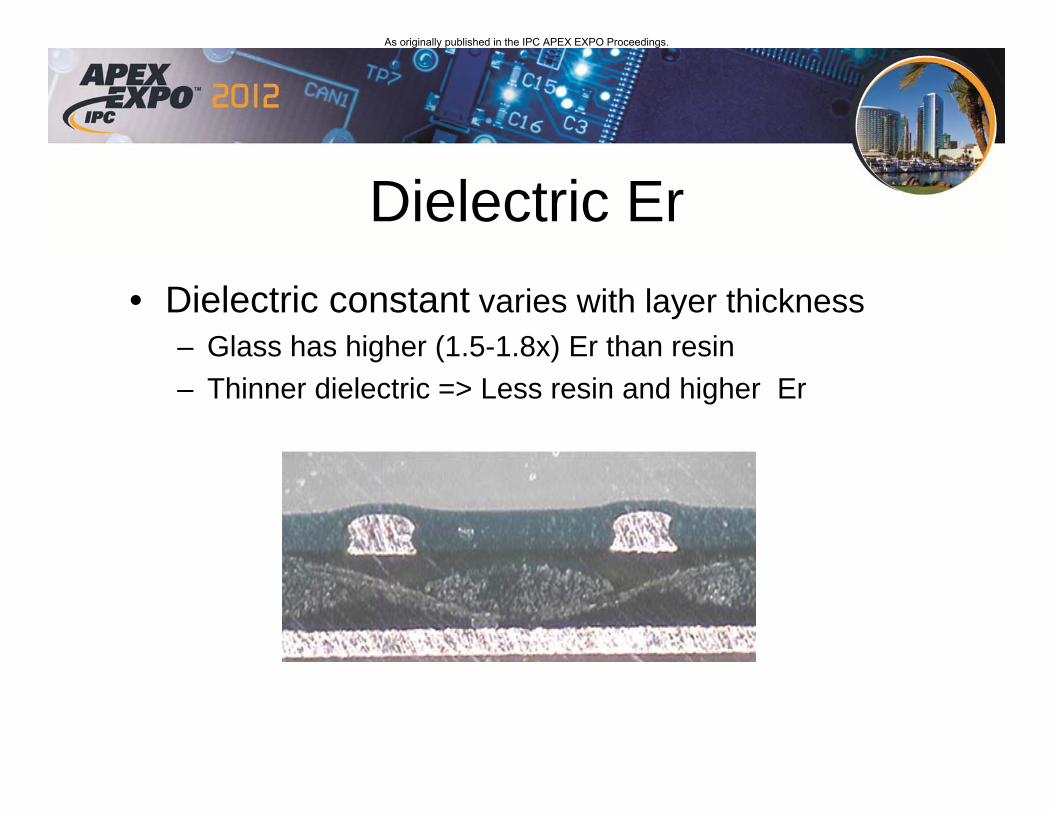
Dielectric Er• Dielectric constant varies with layer thickness
– Glass has higher (1.5-1.8x) Er than resin– Thinner dielectric => Less resin and higher Er
As originally published in the IPC APEX EXPO Proceedings.

Impedance Coupon Challenge• Impedance shift at Center of Void set by design• Coupon design must mimic Partial POOL region
– CMD/ADDR/CLK at center of void - always shifted low– Max DDR byte lane impedance swing at edge of transition region
CMD/ADDR/CLKData regionData region
Transition Region
Center of Void
As originally published in the IPC APEX EXPO Proceedings.

Agenda• Design Example: Partial POOL PCB
• PCB structural behavior affecting impedance
• Impedance coupon considerations
• Call to Action
As originally published in the IPC APEX EXPO Proceedings.

• Impedance coupon attributes typically controlled by PCB fabricator
– Copper density– Trace placement– Coupon location
Zo Coupon Design Considerations
Border Design
Image
Panel Fill
ImpedanceCoupon
ManufacturingCoupons
Typical PCB Manufacturing Panel
As originally published in the IPC APEX EXPO Proceedings.

Impedance Coupon Design• Copper density
control
– Must match IO bus density
– Optimized coupon achieves dielectric height
Std Coupon Optimized Coupon
Cross-section line
0
25
50
75
100
1
1.5
2
2.5
3
3.5
Layer 1-2 Dh
Layer3-4 Dh Partial POOL
Layer 3 Copper Density
%mils
Dielectric Height vs Copper Density across fabrication panel
As originally published in the IPC APEX EXPO Proceedings.

Impedance Coupon Design• Trace placement
selected to match IO bus region
– Center of coupon used for CMD/ADDR/CLK
– Edge traces used to reflect max impedance for Data
2
2.5
3
3.5 Layer 1-2
Layer 3-4Partial POOL
Center Void Ave Thickness
Cross-section
line
mils
Optimized coupon Dielectric Height
As originally published in the IPC APEX EXPO Proceedings.

Impedance Coupon Design• Width of Coupon
critical
– Narrow voids limit thickness transition
– Narrow voids result in impedance coupon shift
2
2.5
3
3.5Layer 1-2
Layer 3-4Partial POOL
Cross-section line
Narrow Coupon Dielectric Height
mils
Center VoidAve Thickness
As originally published in the IPC APEX EXPO Proceedings.

Impedance Coupon Placement• Placement affects
dielectric thickness
– Dielectric height reduced at panel edges
– Best coupon placement at center of the manufacturing panel
mils
Dielectric Height across fabrication panel
Cross-section line
0
20
40
60
80
100
2
2.5
3
3.5
mils
Layer 1-2 Dh Layer 3-4 DhLayer 3 Copper Density
%
Layer 1-2 Dh typical
As originally published in the IPC APEX EXPO Proceedings.

Impedance Coupon on Plated Layers
• Copper density impacts plated trace thickness
– Impacts deposition rate
– Coupon needs to match density of target bus area.
Coupon:Low Cu DensityThickness 2.4-2.6mils
Image:Mid Cu DensityThickness 1.65+/-.1 mils
Image:Cu Fill/PlaneThickness 1.4-1.5mils
Copper Thickness post Pattern Plating of PCB
As originally published in the IPC APEX EXPO Proceedings.

Agenda• Design Example: Partial POOL PCB
• PCB structural behavior affecting impedance
• Impedance coupon considerations
• Call to Action
As originally published in the IPC APEX EXPO Proceedings.

Call to Action
• Impedance coupons must be optimized for copperdensity, panel placement and trace location toprevent systematic impedance shift with respect tothe IO bus
• Copper density transitions impact impedances onmultiple layers and must be considered in all PCBdesigns. Power shapes on signal layers, isolatedbusses, plane splits, etc are potential sources ofcopper density transitions that impact impedances
As originally published in the IPC APEX EXPO Proceedings.

Q&A
As originally published in the IPC APEX EXPO Proceedings.