pci express graphics-class backplanes 1.3) express® graphics-class backplanes (picmg ®1.3)...
TRANSCRIPT

PCI EXPRESS®
GRAPHICS-CLASS
BACKPLANES
(PICMG® 1.3)
Revision HJune 1, 2009
TECHNICAL REFERENCE

WARRANTY The following is an abbreviated version of Chassis Plans’ warranty policy for PICMG 1.3 products. For a
complete warranty statement, contact Chassis Plans or visit our website at www.Chassis-Plans.com.
Chassis Plans PICMG 1.3 products are warranted against material and manufacturing defects for five
years from date of delivery to the original purchaser. Buyer agrees that if this product proves defective
Chassis Plans is only obligated to repair, replace or refund the purchase price of this product at Chassis
Plans’ discretion. The warranty is void if the product has been subjected to alteration, neglect, misuse or
abuse; if any repairs have been attempted by anyone other than Chassis Plans; or if failure is caused by
accident, acts of God, or other causes beyond the control of Chassis Plans Chassis Plans reserves the right
to make changes or improvements in any product without incurring any obligation to similarly alter
products previously purchased.
In no event shall Chassis Plans be liable for any defect in hardware or software or loss or inadequacy of
data of any kind, or for any direct, indirect, incidental or consequential damages arising out of or in
connection with the performance or use of the product or information provided. Chassis Plans’ liability
shall in no event exceed the purchase price of the product purchased hereunder. The foregoing limitation
of liability shall be equally applicable to any service provided by Chassis Plans.
RETURN POLICY Products returned for repair must be accompanied by a Return Material Authorization (RMA) number,
obtained from Chassis Plans prior to return. Freight on all returned items must be prepaid by the customer,
and the customer is responsible for any loss or damage caused by common carrier in transit. Items will be
returned from Chassis Plans via Ground, unless prior arrangements are made by the customer for an alter-
native shipping method
To obtain an RMA number, call us at (858) 57104330. We will need the following information:
Return company address and contact
Model name and model # from the label on the back of the product
Serial number from the label on the back of the product
Description of the failure
An RMA number will be issued. Mark the RMA number clearly on the outside of each box, include a
failure report for each board and return the product(s) to our San Diego, CA facility:
Chassis Plans
8295 Aero Place
San Diego, CA 92123
Attn: Repair Department
Contact Chassis Plans for our complete service and repair policy.

TRADEMARKSIBM, PC/AT, VGA, EGA, OS/2 and PS/2 are trademarks or registered trademarks
of International Business Machines Corp.
Intel is a registered trademark of Intel Corporation.
MS-DOS and Microsoft are registered trademarks of Microsoft Corp.
PICMG, SHB Express and the PICMG logo are trademarks or registered trademarks
of the PCI Industrial Computer Manufacturers Group.
All other brand and product names may be trademarks or registered trademarks
of their respective companies.
LIABILITY DISCLAIMERThis manual is as complete and factual as possible at the time of printing; however, the information in this
manual may have been updated since that time. Chassis Plans reserves the right to change the functions,
features or specifications of their products at any time, without notice.
Copyright © 2009 by Chassis Plans All rights reserved.
E-mail: [email protected]
Web: www.Chassis-Plans.com
Chassis Plans
8295 Aero Place • San Diego, CA 92123Sales: (858) 571-4330 • Fax: (858) 571-6146 • Web: www.Chassis-Plans.com

PCI Express® Backplanes Technical Reference
Chassis Plans
Table of Contents
BEFORE YOU BEGIN .......................................................................... II
INTRODUCTION ....................................................................................... II PCI EXPRESS
® LINKS .............................................................................. II
SHB AND PICMG® 1.3 BACKPLANE CONFIGURATIONS ......................... II
OPTIONAL I/O CONNECTIONS ................................................................. II PCI SLOTS ............................................................................................. III
POWER CONNECTION ............................................................................ III
+12V AUXILIARY POWER CONNECTION ................................................ III POWER CAUTIONS ................................................................................. III
BACKPLANE HOLE PATTERNS ............................................................... III
FOR MORE INFORMATION ..................................................................... III
CHAPTER 1 - BACKPLANE OVERVIEW ....................................... 1-1
INTRODUCTION .................................................................................... 1-1
MODELS .............................................................................................. 1-1
FEATURES ........................................................................................... 1-3
CHAPTER 2 - ISA/PCI REFERENCE ............................................... 2-1
ISA BUS PIN NUMBERING ................................................................... 2-1
ISA BUS PIN ASSIGNMENTS ................................................................ 2-2
ISA BUS SIGNAL DESCRIPTIONS ......................................................... 2-3
I/O ADDRESS MAP* ............................................................................. 2-6
INTERRUPT ASSIGNMENTS* ................................................................. 2-6
PCI LOCAL BUS OVERVIEW ................................................................ 2-7
PCI LOCAL BUS SIGNAL DEFINITION .................................................. 2-8
PCI LOCAL BUS PIN NUMBERING ........................................................ 2-9
PCI LOCAL BUS PIN ASSIGNMENTS ................................................... 2-10
PCI LOCAL BUS SIGNAL DESCRIPTIONS ............................................ 2-13
CHAPTER 3 - PCI EXPRESS® REFERENCE .................................. 3-1
INTRODUCTION .................................................................................... 3-1
PCI EXPRESS®
LINKS........................................................................... 3-1
SHB AND PICMG® 1.3 BACKPLANE CONFIGURATIONS ...................... 3-2
PCI EXPRESS EDGE CONNECTOR PIN ASSIGNMENTS........................... 3-3
PCI EXPRESS SIGNALS OVERVIEW ...................................................... 3-5
POWER CONNECTION .......................................................................... 3-7
POWER SUPPLY AND SHB INTERACTION ............................................. 3-7
ELECTRICAL CONNECTION CONFIGURATIONS ..................................... 3-8
CHAPTER 4 - GRAPHICS-CLASS BACKPLANES ....................... 4-1
S6532-000 BPG2/2 ....................................................................... 4-1
S6537-000 BPG4 .......................................................................... 4-9
S6544-000 BPG6544 ...................................................................4-19
S6600-000 BPG6600 ...................................................................4-33
S6615-000 BPG6615 ...................................................................4-46
S6714-000 BPG6714 ...................................................................4-54
CHAPTER 5 - SERVER-CLASS BACKPLANES ............................ 5-1
S6377-000 BPX3/8 ....................................................................... 5-1
S6467-000 BPX3/14 ....................................................................5-14
S6510-000 BPX5 .........................................................................5-28
S6526-000 BPX3/2 ......................................................................5-38
S6571-000 BPX6571 ...................................................................5-46
S6610-000 BPX6610 ....................................................................5-58
S6620-000 BPX6620 ...................................................................5-66
S6719-000 BPX6719 ...................................................................5-78
S6806-000 BPX6806 ...................................................................5-84
CHAPTER 6 - MULTIPLE SHB SEGMENT BACKPLANES ........ 6-1
S6605-000 BP6FS6605 ................................................................ 6-1
CHAPTER 7 - 2U BUTTERFLY BACKPLA NES ............................ 7-1
S6741-000 BPG6741 ..................................................................... 7-1
PCI Express® Backplanes Technical Reference Backplane Overview
i Chassis Plans
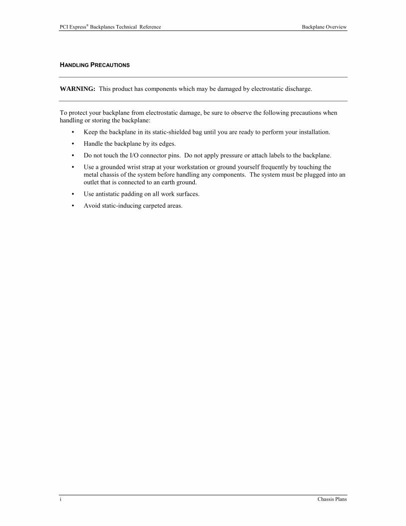
HANDLING PRECAUTIONS WARNING: This product has components which may be damaged by electrostatic discharge.
To protect your backplane from electrostatic damage, be sure to observe the following precautions when
handling or storing the backplane:
• Keep the backplane in its static-shielded bag until you are ready to perform your installation.
• Handle the backplane by its edges.
• Do not touch the I/O connector pins. Do not apply pressure or attach labels to the backplane.
• Use a grounded wrist strap at your workstation or ground yourself frequently by touching the
metal chassis of the system before handling any components. The system must be plugged into an
outlet that is connected to an earth ground.
• Use antistatic padding on all work surfaces.
• Avoid static-inducing carpeted areas.

Backplane Overview PCI Express® Backplanes Technical Reference
Chassis Plans ii
Before You Begin
INTRODUCTION It is important to be aware of the system considerations listed below before installing your Chassis Plans
PCI Express®
backplane. Overall system performance may be affected by incorrect usage of these features.
PCI EXPRESS® LINKS PCI Express devices with different PCI Express link configurations can establish communication using a
process called auto-negotiation or link training. If a board with a higher number of lanes is placed in a slot
with a lower number of lanes (e.g., a x16 board in a x16 mechanical slot electrically configured with a x4
PCIe link) or a board with a lower number of lanes is placed into a slot with a higher number of lanes (e.g.,
a x4 board into a x8 slot), the PCI Express link auto-negotiates down to the lower link rate to establish
communication to the system host board (SHB). The mechanical option card slots on Chassis Plans
PICMG®
1.3 backplanes have PCI Express configuration straps. Some SHB designs may utilize the straps
in the PCI Express link width negotiation process.
SHB AND PICMG® 1.3 BACKPLANE CONFIGURATIONS Chassis Plans’s BPG4 (S6537-xxx), BPG2/2 (S6532-xxx), BPG6544 (S6544-xxx) and BPG6600 (S6600-
xxx), BPG6615 (S6615- xxx), BPG6714 (S6714- xxx) and BPG6741 (S6741- xxx) backplanes support a
graphics-class configuration of the PCI Express links. In this type of configuration, the SHB supports one
x16 PCI Express link and a single x4 link to the graphics-class backplane. These backplanes also support
an additional x1 link when using Chassis Plans’s IOB31 I/O expansion board on a Chassis Plans graphics-
class SHB. The letter “G” in a Chassis Plans backplane model name indicates a graphics-class
configuration.
Chassis Plans’ BPX3/8 (S6377-xxx), BPX3/14 (S6467-xxx), BPX5 (S6510-xxx), BPX3/2 (S6526- xxx),
BPX6571 (S6571-xxx) and BPX6620 (S6620-xxx), BPX6610 (S6610- xxx), BPX6719 (S6719- xxx) and
BPX6736 (S6736- xxx) fall into the server class of PICMG 1.3 compatible backplanes. Server-class
backplanes are designed to maximize the number of x4 and x8 PCI Express links between the SHB and the
backplane. Some backplanes also support an additional x4 link when using Chassis Plans’ IOB31 (S6474-
000) I/O expansion board on a Chassis Plans server-class SHB. The letter “X” in a Chassis Plans’
backplane model name indicates a server-class backplane.
NOTE: Graphics-class SHBs should always be used with graphics-class PICMG 1.3 backplanes and
server-class SHBs should always be used with server-class PICMG 1.3 backplanes. Combining
incompatible SHBs and backplanes will not cause damage to the option cards or SHB, but one or more of
the slots may not function and may result in one or more PCI Express option cards on the backplane being
non-functional. This is due to the fact that there may not be enough available links to properly connect all
of the PCI Express option card slots to the SHB.
OPTIONAL I/O CONNECTIONS The PICMG 1.3 specification enables SHB vendors to route I/O connections to edge connector C of an
SHB. Chassis Plans PICMG 1.3 backplanes support the four USB and two Ethernet connections, but since
these connections are optional, not all SHBs support them. In order to take advantage of these I/O features,
the SHB in your system must be able to support the connections as specified in the PCI Industrial
Manufacturers Group’s SHB Express™ System Host Board PCI Express Specification, PICMG® 1.3.

PCI Express® Backplanes Technical Reference Backplane Overview
iii Chassis Plans
PCI SLOTS PCI slots are managed by edge connector D (closest to the front edge of the SHB). Not all SHBs provide
support for Connector D and will not support PCI slots in those backplanes that provide them. PCI-X slots
are managed by a PCI-E to PCI-X bridge chip and will function. At this writing, the MCXT, MCGT, SLT
and NLT (and their single processor versions) will not support PCI slots. The TQ9, TML and T4L do
support PCI slots on PICMG 1.3 backplanes.
POWER CONNECTION Chassis Plans’s PCI Express backplanes support soft power control signals via the Advanced Configuration
and Power Interface (ACPI) as defined in the PICMG 1.3 specification. When soft control signals are
implemented, the type of ATX or EPS power supply used in the system and the operating system software
will dictate how system power should be connected to the SHB. It is critical that the correct method be
used.
+12V AUXILIARY POWER CONNECTION Chassis Plans PICMG 1.3 backplanes provide one or more +12V power connectors for routing auxiliary
power to the SHB’s edge connectors, eliminating the need for auxiliary power connections on the system
host board. These are 8-pin connectors that can accommodate either a 4-pin or 8-pin power cable
connection.
POWER CAUTIONS
CAUTION: Chassis Plans recommends using EPS model power supplies with its PICMG 1.3 backplanes
in systems using high-performance, dual-processor SHB Express system host boards.
The power needs of backplane option cards, high-performance processors and other system components
may result in drawing 20A of current from the +12V power supply line. If this occurs, hazardous energy
(240VA) could exist inside the system chassis. Final system/equipment suppliers must provide protection
to service personnel from these potentially hazardous energy levels.
Standby voltages may be used in the final system design to enable certain system recovery operations. In
this case, the power supply may not completely remove power to the system host board when the power
switch is turned off. Caution must be taken to ensure that incoming system power is completely
disconnected before removing the system host board.
In some ATX/EPS systems, the power may appear to be off while the 5VSB signal is still present and
supplying power to the SHB, option cards and other system components. The +5VAUX LED on a Chassis
Plans PICMG 1.3 backplane monitors the 5VSB power signal; “green” indicates that the 5VSB signal is
present. Chassis Plans backplane LEDs monitor all DC power signals, and all of the LEDs should be off
before adding or removing components. Removing boards under power may result in system damage.
BACKPLANE HOLE PATTERNS The PICMG 1.3 specification defines recommended backplane sizes and hole patterns. These hole patterns
are not the same as motherboard hole patterns. Chassis Plans’s backplanes support Chassis Plans’s hole
patterns for 14-slot (64-bit) and 20-slot (64-bit) backplanes as well as the hole patterns specified for
PICMG 1.3 backplanes. The Chassis Plans 14-slot hole pattern on the BPX3/8 backplane is modified
slightly to accommodate the backplane’s smaller width dimension. The backplane chapters in this manual
contain mechanical dimensions and hole patterns for individual Chassis Plans PCI Express backplanes.
FOR MORE INFORMATION For more information on any of these features, refer to the appropriate sections of this manual. The latest
revision of this manual may be found on Chassis Plans’s website - www.Chassis-Plans.com.

Backplane Overview PCI Express® Backplanes Technical Reference
Chassis Plans iv
This page intentionally left blank.
PCI Express®Backplanes Technical Reference ISA/PCI Reference
1-1 Chassis Plans
Chapter 1 - Backplane Overview
INTRODUCTION Chassis Plans PCI Express graphics-class and server-class backplanes are six-layer or eight-layer
backplanes which are PICMG 1.3 compatible and allow the use of standard PCI Express, PCI-X, PCI or
ISA option cards. Types and numbers of option cards supported vary depending on the backplane model.
Each backplane has one PCI Express slot which accepts an SHB Express™
system host board (SHB). The
backplanes have a varying number of PCI Express slots available for use.
NOTE: On some of the backplanes, one of the PCI Express slots connects to a PCI Express expansion slot
(PCIeS) on the backplane. In order to use this PCIe slot when you are using a Chassis Plans PCI Express
SHB, you must have a Chassis Plans IOB31 (6474-000) I/O expansion board on the SHB. The IOB31
enables communication between the SHB and the PCI Express slot by providing a x1 or x4 PCI Express
link to the PCIeS slot, depending on the capabilities of the SHB.
Refer to the backplane descriptions in the following chapters of this manual for more information about a
specific backplane.
MODELS
NOTE: In the chart below, the descriptions of the PCI Express slots include the electrical link rate of the
slots, not the mechanical size.
Model # Model Name Graphics-Class Backplanes:
Description
S6532-000
BPG2/2
1 SHB Slot,
1 x16 PCI Express,
2 PCI-X 64-bit/133MHz
S6537-000
BPG4
1 SHB Slot,
1 x16 PCI Express,
1 x4 PCI Express,
1 x1 PCI Express via a PCIe Expansion Slot
S6544-000
BPG6544
1 SHB Slot,
1 x16 PCI Express,
1 z4/x1 PCI Express via a PCIe Expansion Slot,
1 PCI-X 64-bit/133MHz,
4 PCI-X 64-bit/66MHz,
2 PCI 32-bit/33MHz,
2 ISA 32-bit/33MHz

ISA/PCI Reference PCI Express® Backplanes Technical Reference
Chassis Plans 1-2
Model # Model Name Graphics-Class Backplanes: (Continued)
Description
S6600-000
BPG6600
1 SHB Slot,
1 x16 PCI Express,
1 x4/x1 PCI Express via a PCIe Expansion Slot,
2 PCI-X 64-bit/100MHz,
4 PCI-X 64-bit/66MHz,
4 PCI 32-bit/33MHz
S6615-000
BPG6615
1 SHB Slot,
1 x16 PCI Express,
4 x4 PCI Express,
2 PCI-X 64-bit/100MHz,
4 PCI-X 64-bit/66MHz
S6714-000
BPG6714
1 SHB Slot,
1 x16 PCI Express,
1 x4 PCI Express,
1 x4/x1 PCI Express via a PCIe Expansion Slot,
1 PCI-X 64-bit/133MHz,
2 PCI-X 64-bit/100MHz
Model # Model Name Server-Class Backplanes:
Description
S6377-000
BPX3/8
1 SHB Slot,
2 x8 PCI Express,
4 PCI-X 64-bit/66MHz,
4 PCI 64-bit/33MHz
S6467-000
BPX3/14
1 SHB Slot,
1 x4 PCI Express,
1 x4 PCI Express via a PCIe Expansion Slot,
2 PCI-X 64-bit/133MHz,
12 PCI-X 64-bit/100MHz
S6510-000
BPX5
1 SHB Slot,
2 x8 PCI Express,
1 x4 PCI Express,
1 x4 PCI Express via a PCIe Expansion Slot
S6526-000
BPX3/2
1 SHB Slot,
2 x8 PCI Express,
2 PCI-X 64-bit/133MHz
S6571-000
BPX6571
1 SHB Slot,
1 x8 PCI Express,
1 x4 PCI Express,
16 PCI-X 64-bit/66MHz

PCI Express®Backplanes Technical Reference ISA/PCI Reference
1-3 Chassis Plans
Model # Model Name Server-Class Backplanes (continued):
Description
S6610-000 BPX6610 1 SHB Slot
2 x8 PCI Express,
4 x4 PCI Express,
2 PCI-X 64-bit/100MHz
4 PCI-X 64-bit/66MHz
S6620-000
BPX6620
1 SHB Slot,
1 x8 PCI Express,
1 x4 PCI Express via a PCIe Expansion Slot,
2 PCI-X 64-bit/133MHz,
8 PCI-X 64-bit/100MHz
S6719-000 BPX6719 1 SHB Slot,
2 x8 PCI Express,
1 x4 PCI Express via a PCIe Expansion Slot,
1 PCI-X 64-bit/133MHz,
2 PCI-X 64-bit/100MHz
S6806-000 BPX6806 1 SHB Slot,
1 x4 PCI Express,
1 x4 PCI Express via a PCIe Expansion Slot,
12 x4 PCI Expresss via PCIe Fan Out Switch,
4 x8 PCI Express via PCIe Fan Out Switch
Model # Model Name Mutilple SHB -Class Backplanes
Description
S6605-000
BP6FS6605
6 SHB Slot,
6 x16 PCI Express,
3 x4 PCI Express
2U Butterfly -Class Backplanes S6741-000 BPG6741 1 SHB Slot,
1 x16 PCI Express,
2 x1 PCI Express
FEATURES
• Six-layer or eight-layer printed circuit board
• High noise immunity construction
• Accept system host boards (SHBs) which are PCI Industrial Computer Manufacturers Group
(PICMG) 1.3 compatible
• Allow use of standard PCI Express, PCI-X, PCI or ISA option cards, depending on model
• Multiple power supply connectors, depending on model

ISA/PCI Reference PCI Express® Backplanes Technical Reference
Chassis Plans 1-4
This page intentionally left blank.

PCI Express®Backplanes Technical Reference ISA/PCI Reference
2-1 Chassis Plans
Chapter 2 - ISA/PCI Reference
ISA BUS PIN NUMBERING
62-pin ISA Bus Connector
Component Side of Board
36-pin ISA Bus Connector
ISA/PCI Reference PCI Express® Backplanes Technical Reference
Chassis Plans 2-2
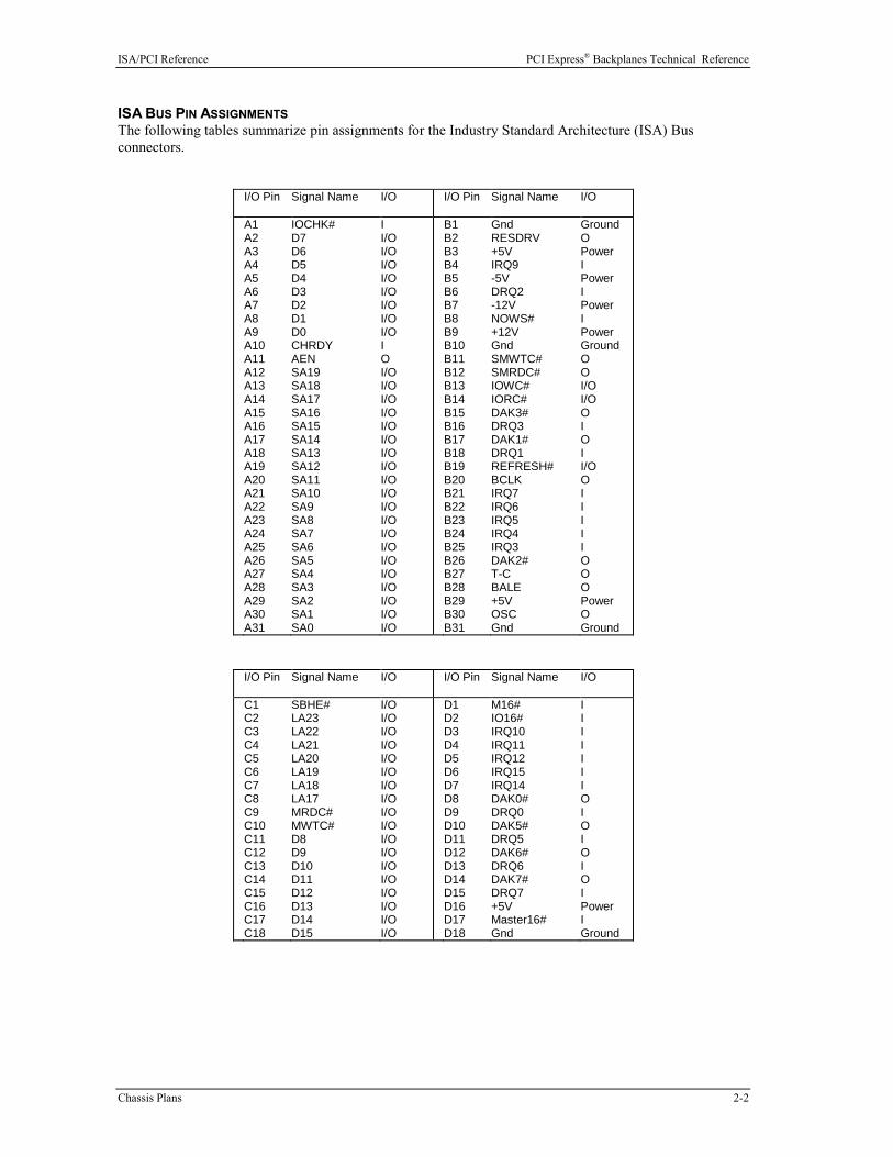
ISA BUS PIN ASSIGNMENTS The following tables summarize pin assignments for the Industry Standard Architecture (ISA) Bus
connectors.
I/O Pin Signal Name I/O I/O Pin Signal Name I/O
A1 A2 A3 A4 A5 A6 A7 A8 A9 A10 A11 A12 A13 A14 A15 A16 A17 A18 A19 A20 A21 A22 A23 A24 A25 A26 A27 A28 A29 A30 A31
IOCHK# D7 D6 D5 D4 D3 D2 D1 D0 CHRDY AEN SA19 SA18 SA17 SA16 SA15 SA14 SA13 SA12 SA11 SA10 SA9 SA8 SA7 SA6 SA5 SA4 SA3 SA2 SA1 SA0
I I/O I/O I/O I/O I/O I/O I/O I/O I O I/O I/O I/O I/O I/O I/O I/O I/O I/O I/O I/O I/O I/O I/O I/O I/O I/O I/O I/O I/O
B1 B2 B3 B4 B5 B6 B7 B8 B9 B10 B11 B12 B13 B14 B15 B16 B17 B18 B19 B20 B21 B22 B23 B24 B25 B26 B27 B28 B29 B30 B31
Gnd RESDRV +5V IRQ9 -5V DRQ2 -12V NOWS# +12V Gnd SMWTC# SMRDC# IOWC# IORC# DAK3# DRQ3 DAK1# DRQ1 REFRESH# BCLK IRQ7 IRQ6 IRQ5 IRQ4 IRQ3 DAK2# T-C BALE +5V OSC Gnd
Ground O Power I Power I Power I Power Ground O O I/O I/O O I O I I/O O I I I I I O O O Power O Ground
I/O Pin Signal Name I/O I/O Pin Signal Name I/O
C1 C2 C3 C4 C5 C6 C7 C8 C9 C10 C11 C12 C13 C14 C15 C16 C17 C18
SBHE# LA23 LA22 LA21 LA20 LA19 LA18 LA17 MRDC# MWTC# D8 D9 D10 D11 D12 D13 D14 D15
I/O I/O I/O I/O I/O I/O I/O I/O I/O I/O I/O I/O I/O I/O I/O I/O I/O I/O
D1 D2 D3 D4 D5 D6 D7 D8 D9 D10 D11 D12 D13 D14 D15 D16 D17 D18
M16# IO16# IRQ10 IRQ11 IRQ12 IRQ15 IRQ14 DAK0# DRQ0 DAK5# DRQ5 DAK6# DRQ6 DAK7# DRQ7 +5V Master16# Gnd
I I I I I I I O I O I O I O I Power I Ground

PCI Express®Backplanes Technical Reference ISA/PCI Reference
2-3 Chassis Plans
ISA BUS SIGNAL DESCRIPTIONS The following is a description of the ISA Bus signals. All signal lines are TTL- compatible.
AEN (O)
Address Enable (AEN) is used to degate the microprocessor and other devices from the I/O channel to
allow DMA transfers to take place. When this line is active, the DMA controller has control of the address
bus, the data-bus Read command lines (memory and I/O), and the Write command lines (memory and I/O).
BALE (O) (Buffered)
Address Latch Enable (BALE) is provided by the bus controller and is used on the system board to latch
valid addresses and memory decodes from the microprocessor. It is available to the I/O channel as an
indicator of a valid microprocessor or DMA address (when used with AEN). Microprocessor addresses
SA[19::0] are latched with the falling edge of BALE. BALE is forced high during DMA cycles.
BCLK (O)
BCLK is the system clock. The clock has a 50% duty cycle. This signal should only be used for
synchronization. It is not intended for uses requiring a fixed frequency.
CHRDY (I)
I/O Channel Ready (CHRDY) is pulled low (not ready) by a memory or I/O device to lengthen I/ O or
memory cycles. Any slow device using this line should drive it low immediately upon detecting its valid
address and a Read or Write command. Machine cycles are extended by an integral number of clock
cycles. This signal should be held low for no more than 2.5 microseconds.
D[15::0] (I/O)
Data signals D[15::0] provide bus bits 15 through 0 for the microprocessor, memory, and I/O devices. D15
is the most-significant bit and D0 is the least-significant bit. All 8-bit devices on the I/O channel should
use D[7::0] for communications to the microprocessor. The 16-bit devices will use D[15::0]. To support 8-
bit devices, the data on D[15::8] will be gated to D[7::0] during 8-bit transfers to these devices. 16-bit
microprocessor transfers to 8-bit devices will be converted to two 8-bit transfers.
DAK[7::5]#, DAK[3::0]# (O)
DMA Acknowledge DAK[7::5]# and DAK[3::0]# are used to acknowledge DMA requests DRQ[7::5] and
DRQ[3::0]. They are active low.
DRQ[7::5], DRQ[3::0] (I)
DMA Requests DRQ[7::5] and DRQ[3::0] are asynchronous channel requests used by peripheral devices
and the I/O channel microprocessors to gain DMA service (or control of the system). They are prioritized,
with DRQ0 having the highest priority and DRQ7 having the lowest. A request is generated by bringing a
DRQ line to an active level. A DRQ line must be held high until the corresponding DMA Request
Acknowledge (DAK) line goes active. DRQ[3::0] will perform 8-bit DMA transfers; DRQ[7::5] will
perform 16-bit transfers.

ISA/PCI Reference PCI Express® Backplanes Technical Reference
Chassis Plans 2-4
IO16# (I)
I/O 16-bit Chip Select (IO16#) signals the system board that the present data transfer is a 16-bit, 1 wait-
state, I/O cycle. It is derived from an address decode. IO16# is active low and should be driven with an
open collector or tri-state driver capable of sinking 20 mAmps.
IOCHK# (I)
I/O Channel Check (IOCHK#) provides the system board with parity (error) information about memory or
devices on the I/O channel. When this signal is active, it indicates an uncorrectable system error.
IORC# (I/O )
I/O Read (IORC#) instructs an I/O device to drive its data onto the data bus. It may be driven by the
system microprocessor or DMA controller, or by a microprocessor or DMA controller resident on the I/O
channel. This signal is active low.
IOWC# (I/O)
I/O Write (IOWC#) instructs an I/O device to read the data on the data bus. It may be driven by any
microprocessor or DMA controller in the system. This signal is active low.
IRQ[15::14], IRQ[12::9], IRQ[7::3] (I)
Interrupt Requests IRQ[15::14], IRQ[12::9] and IRQ[7::3] are used to signal the microprocessor that an I/O
device needs attention. The interrupt requests are prioritized, with IRQ[15::14] and IRQ[12::9] having the
highest priority (IRQ9 is the highest) and IRQ[7::3] having the lowest priority (IRQ7 is the lowest). An
interrupt request is generated when an IRQ line is raised from low to high. The line must be held high until
the microprocessor acknowledges the interrupt request (Interrupt Service routine).
LA[23::17] (I/O)
These signals (unlatched) are used to address memory and I/O devices within the system. They give the
system up to 16MB of addressability. These signals are valid when BALE is high. LA[23::17] are not
latched during microprocessor cycles and therefore do not stay valid for the whole cycle. Their purpose is
to generate memory decodes for 1 wait-state memory cycles. These decodes should be latched by I/O
adapters on the falling edge of BALE. These signals also may be driven by other microprocessors or DMA
controllers that reside on the I/O channel.
M16# (I)
M16# Chip Select signals the system board if the present data transfer is a 1<N>wait-state, 16- bit, memory
cycle. It must be derived from the decode of LA[23::17]. M16# should be driven with an open collector or
tri-state driver capable of sinking 20 mAmps.
Master16# (I)
Master16# is used with a DRQ line to gain control of the system. A processor or DMA controller on the
I/O channel may issue a DRQ to a DMA channel in cascade mode and receive a DAK#. Upon receiving
the DAK#, an I/O microprocessor may pull Master16# low, which will allow it to control the system
address, data, and control lines (a condition known as tri-state). After Master16# is low, the I/O
microprocessor must wait one system clock period before driving the address and data lines, and two clock
periods before issuing a Read or Write command. If this signal is held low for more than
15<N>microseconds, system memory may be lost because of a lack of refresh.

PCI Express®Backplanes Technical Reference ISA/PCI Reference
2-5 Chassis Plans
NOWS# (I) The No Wait State (NOWS#) signal tells the microprocessor that it can complete the present bus cycle without inserting any additional wait cycles. In order to run a memory cycle to a 16-bit device without wait cycles, NOWS# is derived from an address decode gated with a Read or Write command. In order to run a memory cycle to an 8-bit device with a minimum of two wait states, NOWS# should be driven active on system clock after the Read or Write command is active gated with the address decode for the device. Memory Read and Write commands to a 8-bit device are active on the falling edge of the system clock. NOWS# is active low and should be driven with an open collector or tri-state driver capable of sinking 20 mAmps. OSC (O) Oscillator (OSC) is a high-speed clock with a 70-nanosecond period (14.31818 MHz). This signal is not synchronous with the system clock. It has a 50% duty cycle. REFRESH# (I/O) The REFRESH# signal is used to indicate a refresh cycle and can be driven by a microprocessor on the I/O channel. RESDRV (O) Reset Drive (RESDRV) is used to reset or initialize system logic at power-up time or during a low line-voltage outage. This signal is active high. SA[19::0] (I/O) Address bits SA[19::0] are used to address memory and I/O devices within the system. These twenty address lines, in addition to LA[23::17], allow access of up to 16MB of memory. SA[19::0] are gated on the system bus when BALE is high and are latched on the falling edge of BALE. These signals are generated by the microprocessor or DMA Controller. They also may be driven by other microprocessors or DMA controllers that reside on the I/O channel. SBHE# (I/O) System Bus High Enable (SBHE#) indicates a transfer of data on the upper byte of the data bus, D[15::8]. 16-bit devices use SBHE# to condition data bus buffers tied to D[15::8]. SMRDC# (O), MRDC# (I/O) These signals instruct the memory devices to drive data onto the data bus. SMRDC# is active only when the memory decode is within the low 1MB of memory space. MRDC# is active on all memory read cycles. MRDC# may be driven by any microprocessor or DMA controller in the system. SMRDC is derived from MRDC# and the decode of the low 1MB of memory. When a microprocessor on the I/O channel wishes to drive MRDC#, it must have the address lines valid on the bus for one system clock period before driving MRDC# active. Both signals are active low. SMWTC# (O), MWTC# (I/O) These signals instruct the memory devices to store the data present on the data bus. SMWTC# is active only when the memory decode is within the low 1MB of the memory space. MWTC# is active on all memory write cycles. MWTC# may be driven by any microprocessor or DMA controller in the system. SMWTC# is derived from MWTC# and the decode of the low 1MB of memory. When a microprocessor on the I/O channel wishes to drive MWTC#, it must have the address lines valid on the bus for one system clock period before driving MWTC# active. Both signals are active low.
T-C (O)
Terminal Count (T-C) provides a pulse when the terminal count for any DMA channel is reached.

ISA/PCI Reference PCI Express® Backplanes Technical Reference
Chassis Plans 2-6
I/O ADDRESS MAP*
Hex Range Device
000-01F 020-03F 040-05F 060-06F 070-07F 080-09F 0A0-0BF 0C0-0DF 0F0 0F1 0F8-0FF 1F0-1F8 200-207 278-27F 2F8-2FF 300-31F 360-36F 378-37F 380-38F 3A0-3AF 3B0-3BF 3C0-3CF 3D0-3DF 3F0-3F7 3F8-3FF
DMA Controller 1 Interrupt Controller 1, Master Timer 8042 (Keyboard) Real-time Clock, NMI (non-maskable interrupt) Mask DMA Page Register Interrupt Controller 2 DMA Controller 2 Clear Math Coprocessor Busy Reset Math Coprocessor Math Coprocessor Fixed Disk Game I/O Parallel Printer Port 2 Serial Port 2 Prototype Card Reserved Parallel Printer Port 1 SDLC, Bisynchronous 2 Bisynchronous 1 Monochrome Display and Printer Adapter Reserved Color/Graphics Monitor Adapter Diskette Controller Serial Port 1
INTERRUPT ASSIGNMENTS*
Interrupt Description
IRQ0 IRQ1 IRQ2 IRQ3 IRQ4 IRQ5 IRQ6 IRQ7 IRQ8 IRQ9 IRQ10 IRQ11 IRQ12 IRQ13 IRQ14 IRQ15
Timer Output 0 Keyboard (Output Buffer Full) Interrupt 8 through 15 Serial Port 2 Serial Port 1 Parallel Port 2 Diskette Controller Parallel Port 1 Real-time Clock Interrupt Software Redirected to INT 0AH (IRQ2) Unassigned Unassigned Unassigned Coprocessor Fixed Disk Controller Unassigned
* These are typical parameters, which may not reflect your current system.

PCI Express®Backplanes Technical Reference ISA/PCI Reference
2-7 Chassis Plans
PCI LOCAL BUS OVERVIEW The PCI (Peripheral Component Interconnect) Local Bus is a high performance, 32-bit or 64-bit bus with
multiplexed address and data lines. It is intended for use as an interconnect mechanism between highly
integrated peripheral controller components, peripheral add-in boards and processor/memory systems.
The "local bus" moves peripheral functions with high bandwidth requirements closer to the system’s
processor bus and can produce substantial performance gains with graphical user interfaces (GUIs) and
other high bandwidth functions (i.e., full motion video, SCSI, LANs, etc.).
The PCI Local Bus accommodates future system requirements and is applicable across multiple platforms
and architectures.
The PCI component and add-in card interface is processor independent, enabling an efficient transition to
future processor generations, by bridges or by direct integration, and use with multiple processor
architectures. Processor independence allows the PCI Local Bus to be optimized for I/O functions, enables
concurrent operation of the local bus with the processor/memory subsystem, and accommodates multiple
high performance peripherals in addition to graphics. Movement to enhanced video and multimedia
displays and other high bandwidth I/O will continue to increase local bus bandwidth requirements. A
transparent 64-bit extension of the 32-bit data and address buses is defined, doubling the bus bandwidth and
offering forward and backward compatibility of 32-bit (132MB/s peak) and 64-bit (264MB/s peak) PCI
Local Bus peripherals.
ISA/PCI Reference PCI Express® Backplanes Technical Reference
Chassis Plans 2-8
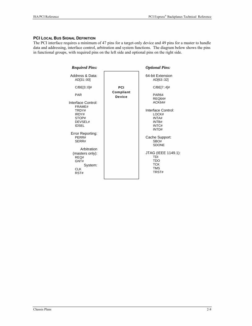
PCI LOCAL BUS SIGNAL DEFINITION The PCI interface requires a minimum of 47 pins for a target-only device and 49 pins for a master to handle
data and addressing, interface control, arbitration and system functions. The diagram below shows the pins
in functional groups, with required pins on the left side and optional pins on the right side.
PCI Pin List
Required Pins:
Address & Data: AD[31::00]
C/BE[3::0]#
PAR
Interface Control:
FRAME# TRDY# IRDY# STOP# DEVSEL# IDSEL
Error Reporting:
PERR# SERR#
Arbitration
(masters only): REQ# GNT#
System: CLK RST#
Optional Pins: 64-bit Extension AD[63::32] C/BE[7::4]# PAR64 REQ64# ACK64# Interface Control: LOCK# INTA# INTB# INTC# INTD# Cache Support: SBO# SDONE JTAG (IEEE 1149.1): TDI TDO TCK TMS TRST#
PCI Compliant
Device

PCI Express®Backplanes Technical Reference ISA/PCI Reference
2-9 Chassis Plans
PCI LOCAL BUS PIN NUMBERING
5-volt/32-bit PCI Connector
Component Side of Board PCI Pin List

ISA/PCI Reference PCI Express® Backplanes Technical Reference
Chassis Plans 2-10
PCI LOCAL BUS PIN ASSIGNMENTS The PCI Local Bus pin assignments shown below are for the PCI option slots on the backplane.
The PCI Local Bus specifies both 5-volt and 3.3-volt signaling environments. The following bus pin
assignments are for the 5-volt connector. The 3.3-volt connector bus pin assignments are the same with the
following exceptions:
* The pins noted as +V (I/O) are +5 volts or +3.3 volts, depending on which connector is being
used.
† Pins B12, B13, A12 and A13 are Gnd (ground) on the 5-volt connector, but are Connector Keys
on the 3.3-volt connector.
†† Pin B49 is Gnd (ground) on the 5-volt connector, but is M66EN on the 3.3- volt connector.
††† Pins B50, B51, A50 and A51 are Connectors Keys on the 5-volt connector, but are Gnd (ground)
on the 3.3-volt connector.
I/O Pin Signal Name I/O Pin Signal Name
B1 B2 B3 B4 B5 B6 B7 B8 B9 B10 B11 B12 B13 B14 B15 B16 B17 B18 B19 B20 B21 B22 B23 B24 B25 B26 B27 B28 B29 B30 B31 B32 B33 B34 B35
-12V TCK Gnd TDO +5V +5V INTB# INTD# PRSNT1# Reserved PRSNT2# Gnd Gnd
Reserved Gnd CLK Gnd REQ# +V (I/O) * AD31 AD29 Gnd AD27 AD25 +3.3V C/BE3# AD23 Gnd AD21 AD19 +3.3V AD17 C/BE2# Gnd IRDY#
A1 A2 A3 A4 A5 A6 A7 A8 A9 A10 A11 A12 A13 A14 A15 A16 A17 A18 A19 A20 A21 A22 A23 A24 A25 A26 A27 A28 A29 A30 A31 A32 A33 A34 A35
TRST# +12V TMS TDI +5V INTA# INTC# +5V Reserved +V (I/O) * Reserved Gnd Gnd Reserved RST# +V (I/O) * GNT# Gnd Reserved AD30 +3.3V AD28 AD26 Gnd AD24 IDSEL +3.3V AD22 AD20 Gnd AD18 AD16 +3.3V FRAME# Gnd
32-bit connector
3.3-Volt Key 3.3-Volt Key

PCI Express®Backplanes Technical Reference ISA/PCI Reference
2-11 Chassis Plans
PCI LOCAL BUS PIN ASSIGNMENTS (CONTINUED)
I/O Pin Signal Name I/O Pin Signal Name
B36 B37 B38 B39 B40 B41 B42 B43 B44 B45 B46 B47 B48 B49
+3.3V DEVSEL# Gnd LOCK# PERR# +3.3V SERR# +3.3V C/BE1# AD14 Gnd AD12 AD10 Gnd
A36 A37 A38 A39 A40 A41 A42 A43 A44 A45 A46 A47 A48 A49
TRDY# Gnd STOP# +3.3V SDONE SBO# Gnd PAR AD15 +3.3V AD13 AD11 Gnd AD9
B50 B51
Connector Key Connector Key
A50 A51
Connector Key Connector Key
5-volt key 5-volt key
B52 B53 B54 B55 B56 B57 B58 B59 B60 B61 B62
AD8 AD7 +3.3V AD5 AD3 Gnd AD1 +V (I/O) * ACK64# +5V +5V
A52 A53 A54 A55 A56 A57 A58 A59 A60 A61 A62
C/BE0# +3.3V AD6 AD4 Gnd AD2 AD0 +V (I/O) * REQ64# +5V +5V
32-bit connector end

ISA/PCI Reference PCI Express® Backplanes Technical Reference
Chassis Plans 2-12
PCI LOCAL BUS PIN ASSIGNMENTS (CONTINUED) The following pin assignments apply only to backplanes with 64-bit PCI option slots.
I/O Pin Signal Name I/O Pin Signal Name
Connector Key Connector Key
Connector Key Connector Key
64-bit spacer 64-bit spacer
B63 B64 B65 B66 B67 B68 B69 B70 B71 B72 B73 B74 B75 B76 B77 B78 B79 B80 B81 B82 B83 B84 B85 B86 B87 B88 B89 B90 B91 B92 B93 B94
Reserved Gnd C/BE6# C/BE4# Gnd AD63 AD61 +V (I/O) * AD59 AD57 Gnd AD55 AD53 Gnd AD51 AD49 +V (I/O) * AD47 AD45 Gnd AD43 AD41 Gnd AD39 AD37 +V (I/O) * AD35 AD33 Gnd Reserved Reserved Gnd
A63 A64 A65 A66 A67 A68 A69 A70 A71 A72 A73 A74 A75 A76 A77 A78 A79 A80 A81 A82 A83 A84 A85 A86 A87 A88 A89 A90 A91 A92 A93 A94
Gnd C/BE7# C/BE5# +V (I/O) * PAR64 AD62 Gnd AD60 AD58 Gnd AD56 AD54 +V (I/O) * AD52 AD50 Gnd AD48 AD46 Gnd AD44 AD42 +V (I/O) * AD40 AD38 Gnd AD36 AD34 Gnd AD32 Reserved Gnd Reserved
64-bit connector start 64-bit connector end

PCI Express®Backplanes Technical Reference ISA/PCI Reference
2-13 Chassis Plans
PCI LOCAL BUS SIGNAL DESCRIPTIONS The PCI Local Bus signals are described below and may be categorized into the following functional
groups:
• System Pins
• Address and Data Pins
• Interface Control Pins
• Arbitration Pins (Bus Masters Only)
• Error Reporting Pins
• Interrupt Pins (Optional)
• Cache Support Pins (Optional)
• 64-Bit Bus Extension Pins (Optional)
• JTAG/Boundary Scan Pins (Optional)
A # symbol at the end of a signal name indicates that the active state occurs when the signal is at a low
voltage. When the # symbol is absent, the signal is active at a high voltage.
The following are descriptions of the PCI Local Bus signals.
ACK64# (optional)
Acknowledge 64-bit Transfer, when actively driven by the device that has positively decoded its address as the target of the current access, indicates the target is willing to transfer data using 64bits. ACK64# has the same timing as DEVSEL#.
AD[31::00]
Address and Data are multiplexed on the same PCI pins. A bus transaction consists of an address phase followed by one or more data phases. During the address phase, AD[31::00] contain a physical address (32 bits). During data phases, AD[07::00] contain the least significant byte (lsb) and AD[31::24] contain the most significant byte (msb).
AD[63::32] (optional)
Address and Data are multiplexed on the same pins and provide 32additional bits. During an address phase (when using the DAC command and when REQ64# is asserted), the upper 32bits of a 64-bit address are transferred; otherwise, these bits are reserved but are stable and indeterminate. During a data phase, an additional 32bits of data are transferred when REQ64# and ACK64# are both asserted.
C/BE[3::0]#
Bus Command and Byte Enables are multiplexed on the same PCI pins. During the address phase of a transaction, these pins define the bus command; during the data phase they are used as byte enables. The byte enables are valid for the entire data phase and determine which byte lanes carry meaningful data. C/BE0# applies to byte0 (lsb) and C/BE3# applies to byte 3 (msb).

ISA/PCI Reference PCI Express® Backplanes Technical Reference
Chassis Plans 2-14
C/BE[7::4]# (optional) Bus Command and Byte Enables are multiplexed on the same pins. During an address phase (when using the DAC command and when REQ64# is asserted), the actual bus command is transferred on C/BE[7::4]#; otherwise, these bits are reserved and indeterminate. During a data phase, C/BE[7::4]# are byte enables indicating which byte lanes carry meaningful data when REQ64# and ACK64# are both asserted. C/BE4# applies to byte4 and C/BE7# applies to byte7.
CLK
Clock provides timing for all transactions on PCI and is an input to every PCI device.
DEVSEL#
Device Select, when actively driven, indicates that the driving device has decoded its address as the target of the current access. As an input, DEVSEL# indicates whether any device on the bus has been selected.
FRAME#
Cycle Frame is an interface control pin which is driven by the current master to indicate the beginning and duration of an access. When FRAME# is asserted, data transfers continue; when it is deasserted, the transaction is in the final data phase.
GNT#
Grant indicates to the agent that access to the bus has been granted. This is a point to point signal. Every master has its own GNT#.
IDSEL
Initialization Device Select is used as a chip select during configuration read and write transactions.
INTA#, INTB#, INTC#, INTD# (optional)
Interrupts on PCI are optional and defined as "level sensitive," asserted low (negative true), using open drain output drivers. PCI defines one interrupt for a single function and up to four interrupt lines for a multi-function device or connector.
Interrupt A is used to request an interrupt. For a single function device, only INTA# may be used, while the other three interrupt lines have no meaning. Interrupt B, Interrupt C and Interrupt D are used to request additional interrupts and only have meaning on a multi-function device.
IRDY#
Initiator Ready indicates the initiating agent’s (bus master’s) ability to complete the current data phase of the transaction. IRDY# is used in conjunction with TRDY#. During a write, IRDY# indicates that valid data is present on AD[31::0]. During a read, it indicates that the master is prepared to accept data.
LOCK#
Lock indicates an operation that may require multiple transactions to complete. When LOCK# is asserted, non-exclusive transactions may proceed to an address that is not currently locked.

PCI Express®Backplanes Technical Reference ISA/PCI Reference
2-15 Chassis Plans
PAR Parity is even parity across AD[31::00] and C/BE[3::0]#. Parity generation is required by all PCI agents. The master drives PAR for address and write data phases; the target drives PAR for read data phases.
PAR64 (optional)
Parity Upper DWORD is the even parity bit that protects AD[63::32] and C/BE[7::4]#. The master drives PAR64 for address and write data phases; the target drives PAR64 for read data phases.
PERR#
Parity Error is for the reporting of data parity errors during all PCI transactions except a Special Cycle. There are no special conditions when a data parity error may be lost or when reporting of an error may be delayed.
PRSNT1# and PRSNT2#
PRSNT1# and PRSNT2# are related to the connector only, not to other PCI components. They are used for two purposes: indicating that a board is physically present in the slot and providing information about the total power requirements of the board.
REQ#
Request indicates to the arbiter that this agent desires use of the bus. This is a point to point signal. Every master has its own REQ#.
REQ64# (optional)
Request 64-bit Transfer, when actively driven by the current bus master, indicates it desires to transfer data using 64 bits. REQ64# has the same timing as FRAME#. REQ64# has meaning at the end of reset.
RST#
Reset is used to bring PCI-specific registers, sequencers and signals to a consistent state.
SBO# (optional)
Snoop Backoff is an optional cache support pin which indicates a hit to a modified line when asserted. When SBO# is deasserted and SDONE is asserted, it indicates a "clean" snoop result.
SDONE (optional)
Snoop Done is an optional cache support pin which indicates the status of the snoop for the current access. When deasserted, it indicates the result of the snoop is still pending. When asserted, it indicates the snoop is complete.
SERR#
System Error is for reporting address parity errors, data parity errors on the Special Cycle command, or any other system error where the result will be catastrophic. If an agent does not want a non-maskable interrupt (NMI) to be generated, a different reporting mechanism is required.

ISA/PCI Reference PCI Express® Backplanes Technical Reference
Chassis Plans 2-16
STOP# Stop indicates that the current target is requesting the master to stop the current transaction.
TCK (optional)
Test Clock is used to clock state information and test data into and out of the device during operation of the TAP (Test Access Port).
TDI (optional)
Test Data Input is used to serially shift test data and test instructions into the device during TAP (Test Access Port) operation.
TDO (optional)
Test Data Output is used to serially shift test data and test instructions out of the device during TAP (Test Access Port) operation.
TMS (optional)
Test Mode Select is used to control the state of the TAP (Test Access Port) controller in the device.
TRDY#
Target Ready indicates the target agent’s (selected device’s) ability to complete the current data phase of the transaction. TRDY# is used in conjunction with IRDY#. During a read, TRDY# indicates that valid data is present on AD[31::00]. During a write, it indicates that the target is prepared to accept data.
TRST# (optional)
Test Reset provides an asynchronous initialization of the TAP controller. This signal is optional in the IEEE Standard Test Access Port and Boundary Scan Architecture.

PCI Express® Backplanes Technical Reference
3-1 Chassis Plans
Chapter 3 - PCI Express ® Reference
INTRODUCTION PCI Express
® is a high-speed, high-bandwidth interface with multiple channels (lanes) bundled together
with each lane using full-duplex, serial data transfers with high clock frequencies.
The PCI Express architecture is based on the conventional PCI addressing model, but improves upon it by
providing a high-performance physical interface and enhanced capabilities. Whereas the PCI bus
architecture provided parallel communication between a processor board and backplane, the PCI Express
protocol provides high-speed serial data transfer, which allows for higher clock speeds. The same data rate
is available in both directions simultaneously, effectively reducing bottlenecks between the system host
board (SHB) and PCI Express option cards.
PCI Express option cards may require updated device drivers. Most operating systems that support legacy
PCI cards will also support PCI Express cards without modification. Because of this design, PCI, PCI-X
and PCI Express option cards can co-exist in the same system.
PCI Express connectors have lower pin counts than PCI bus connectors. The PCIe connectors are
physically different, based on the number of lanes in the connector.
PCI EXPRESS® LINKS Several PCI Express channels (lanes) can be bundled for each expansion slot, leaving room for stages of
expansion.
A basic PCI Express lane consists of a set of differential signal pairs: one pair for transmission and one
pair for reception. A PCI Express link is a collection of one or more PCIe lanes. PCI Express supports
scalable link widths in 1-, 4-, 8- and 16-lane configurations, generally referred to as x1, x4, x8 and x16
slots. A x1 (“by 1”) slot indicates that the slot has one PCIe lane, which gives it a bandwidth of 250MB/s
in each direction. Since devices do not compete for bandwidth, the effective bandwidth, counting
bandwidth in both directions, is 500MB/s (full-duplex).
The number and configuration of an SHB’s PCI Express links is determined by specific component PCI
Express specifications. The bandwidths for the PCIe links are determined by the link width multiplied by
250MB/s and 500MB/s, as follows:
Slot Full-Duplex
Size Bandwidth Bandwidth
x1 250MB/s 500MB/s
x4 1GB/s 2GB/s
x8 2GB/s 4GB/s
x16 4GB/s 8GB/s
Scalability is a core feature of PCI Express. PCI Express interface scalability enables greater system
operational flexibility and efficiency.
PCI Express devices with different PCI Express link configurations can establish communication using a
process called auto-negotiation or link training. If a board with a higher number of lanes is placed in a slot
with a lower number of lanes (e.g., a x16 board in a x1 slot) or a board with a lower number of lanes is
placed into a slot with a higher number of lanes (e.g., a x4 board into a x16 slot), the link auto-negotiates
down to the lower link rate to establish communication. The mechanical option card slots on Chassis Plans
PICMG®
1.3 backplanes have PCI Express configuration straps. Some SHB designs may utilize the straps
in the PCI Express link width negotiation process.
PCI Express® Backplanes Technical Reference
Chassis Plans 3-2
In order to properly support all of the PCI Express option card slots or devices on a PICMG 1.3 backplane,
the SHB must provide an adequate number of both PCI Express links and PCI Express reference clocks.
For more information, refer to the PCI Industrial Manufacturers Group’s SHB Express™ System Host Board PCI Express Specification, PICMG® 1.3.
SHB AND PICMG® 1.3 BACKPLANE CONFIGURATIONS The PICMG 1.3 specification enables SHB vendors to provide multiple PCI Express configuration options
for edge connectors A and B of a particular SHB. These edge connectors carry the PCI Express links and
reference clocks down to the SHB slot on the PICMG 1.3 backplane. The PICMG 1.3 specification states
that the SHB must provide as many reference clocks as there are potential PCI Express links on the PICMG
1.3 backplane.
The potential PCI Express link configurations of an SHB fall into two main classifications: server-class
and graphics-class. The specific class and PCI Express link configuration of an SHB is determined by the
chipset components used on the SHB.
A graphics-class SHB configuration should provide a x16 PCI Express link down to the backplane in order
to support high-end PCI Express graphics and video cards. The graphics-class SHB configuration is
generally identified by one x16 PCIe link and one x4 or four x1 links to the edge connectors.
In a server-class configuration, the main goal of the SHB is to route as many high- bandwidth PCI Express
links as possible down to the backplane. Typically, these links are a combination of x4 and x8 PCI Express
links.
NOTE: Graphics-class SHBs should always be used with graphics-class PICMG 1.3 backplanes and
server-class SHBs should always be used with server-class PICMG 1.3 backplanes. Combining
incompatible SHBs and backplanes will not cause damage to the option cards or SHB, but one or more of
the slots may not function and may result in one or more PCI Express option cards on the backplane being
non-functional. This is due to the fact that there may not be enough available links to properly connect all
of the PCI Express option card slots to the SHB. Precautions have been engineered into the PICMG 1.3
specification to prevent either SHB or backplane damage if this functionality mismatch occurs.
The figures below show some typical SHB and backplane combinations that would result in all of the PCI
Express slots successfully establishing communication with the SHB host device.

PCI Express® Backplanes Technical Reference
3-3 Chassis Plans
PCI Express link configuration straps for each PCI Express option card slot on a PICMG 1.3 backplane are
required as part of the PICMG 1.3 SHB Express™
specification. These configuration straps may be used to
alert the SHB as to the specific link configuration expected on each PCI Express option card slot. PCI
Express communication between the SHB and option card slots is successful only when there are enough
available PCI Express links established between the PICMG 1.3 SHB and each PCI Express slot or device
on the backplane.
For more information, refer to the PCI Industrial Manufacturers Group’s SHB Express™ System Host Board PCI Express Specification, PICMG® 1.3.
PCI EXPRESS EDGE CONNECTOR PIN ASSIGNMENTS Chassis Plans PCI Express server-class backplanes provide edge connectors A, B and C.
Optional I/O signals are defined in the PICMG 1.3 specification and if implemented must be located on
edge connector C of the SHB. Chassis Plans PICMG 1.3 backplanes enable some or all of the USB and
Ethernet connections on edge connector C, but since these connections are optional, not all SHBs support
them. In order to take advantage of these I/O features, the SHB in your system must be able to support the
connections as specified in the PCI Industrial Manufacturers Group’s SHB Express™ System Host Board PCI Express Specification, PICMG® 1.3.
The BPG6544 supports two ISA slots via a PCI-to-ISA bridge chip. Since the ISA bus interface is not part
of the PICMG 1.3 specification, two reserved pins are used to route the ISA signals SERIRQ and
NOGO_ISA to the backplane’s PCI-to-ISA bridge chip. Legacy PCI card support is not impacted by this
ISA bus signal routing requirement. The following bus pin assignments are used:
* SERIRQ -- connector A, pin B77
** NOGO_ISA -- connector B, pin A2
The following table shows pin assignments for the PCI Express edge connectors on Chassis Plans
backplanes. Connector D is only available on graphics-class backplanes.
Connector A Connector B Connector C *Connector D Side B Side A Side B Side A Side B Side A Side B Side A 1 2 3 4 5 6 7 8 9 10 11
SMCLK GND TDI TDO TRST# PWRBT# PWRGD SHB_RST# CFG0 CFG2 RSVD
SMDAT GND TCK TMS WAKE# PME# PSON# PERST# CFG1 CFG3 GND
1 2 3 4 5 6 7 8 9 10 11
+5Vaux GND a_PETp8 a_PETn8 GND GND a_PETp9 a_PETn9 GND GND RSVD
+5Vaux RSVD ** GND GND a_PERp8 a_PERn8 GND GND a_PERp9 a_PERn9 GND
1 2 3 4 5 6 7 8 9 10 11
USB0P USB0N GND GND USB2P USB2N GND GND USBOC0# GND USBOC2#
GND GND USB1P USB1N GND GND USB3P USB3N GND USBOC1# GND
1 2 3 4 5 6 7 8 9 10 11
INTB# INTD# GND REQ3# REQ2# PCI_RST# REQ1# REQ0# SDONE GND CLKFO
INTA# INTC# VIO GNT3# GNT2# GNT1# GNT0# SERR# +3.3V CLKF1 GND
Mechanical Key Mechanical Key Mechanical Key Mechanical Key * Graphics-class backplanes only.

PCI Express® Backplanes Technical Reference
Chassis Plans 3-4
Connector A Connector B Connector C *Connector D Side B Side A Side B Side A Side B Side A Side B Side A 12 13 14 15 16 17 18 19 20 21 22 23 24 25 26 27 28 29 30 31 32 33 34 35 36 37 38 39 40 41 42 43 44 45 46 47 48 49 50 51 52 53 54 55 56 57 58 59 60 61 62 63 64 65 66 67 68 69 70 71 72 73 74 75 76 77 78 79 80 81 82
GND b_PETp0 b_PETn0 GND GND b_PETp1 b_PETn1 GND GND b_PETp2 b_PETn2 GND GND b_PETp3 b_PETn3 GND GND REFCLK0+ REFCLK0- GND RSVD-G REFCLK2+ REFCLK2- GND RSVD-G REFCLK4+ REFCLK4- GND RSVD-G REFCLK6+ REFCLK6- GND GND a_PETp0 a_PETn0 GND GND a_PETp1 a_PETn1 GND GND a_PETp2 a_PETn2 GND GND a_PETp3 a_PETn3 GND GND a_PETp4 a_PETn4 GND GND a_PETp5 a_PETn5 GND GND a_PETp6 a_PETn6 GND GND a_PETp7 a_PETn7 GND GND RSVD * +3.3V +3.3V +3.3V +3.3V +3.3V
RSVD GND GND b_PERp0 b_PERn0 GND GND b_PERp1 b_PERn1 GND GND b_PERp2 b_PERn2 GND GND b_PERp3 b_PERn3 GND GND REFCLK1+ REFCLK1- GND GND REFCLK3+ REFCLK3- GND GND REFCLK5+ REFCLK5- GND GND REFCLK7+ REFCLK7- GND GND a_PERp0 a_PERn0 GND GND a_PERp1 a_PERn1 GND GND a_PERp2 a_PERn2 GND GND a_PERp3 a_PERn3 GND GND a_PERp4 a_PERn4 GND GND a_PERp5 a_PERn5 GND GND a_PERp6 a_PERn6 GND GND a_PERp7 a_PERn7 GND +3.3V +3.3V +3.3V +3.3V +3.3V
12 13 14 15 16 17 18 19 20 21 22 23 24 25 26 27 28 29 30 31 32 33 34 35 36 37 38 39 40 41 42 43 44 45 46 47 48 49
GND a_PETp10 a_PETn10 GND GND a_PETp11 a_PETn11 GND GND a_PETp12 a_PETn12 GND GND a_PETp13 a_PETn13 GND GND a_PETp14 a_PETn14 GND GND a_PETp15 a_PETn15 GND GND RSVD RSVD GND GND GND GND GND +12V +12V +12V +12V +12V +12V
RSVD GND GND a_PER10 a_PERn10 GND GND a_PERp11 a_PERn11 GND GND a_PERp12 a_PERn12 GND GND a_PERp13 a_PERn13 GND GND a_PERp14 a_PERn14 GND GND a_PERp15 a_PERn15 GND RSVD GND GND GND GND GND +12V +12V +12V +12V +12V +12V
12 13 14 15 16 17 18 19 20 21 22 23 24 25 26 27 28 29 30 31 32 33 34 35 36 37 38 39 40 41 42 43 44 45 46 47 48 49 50 51 52 53 54 55 56 57 58 59 60 61 62 63 64 65 66 67 68 69 70 71 72 73 74 75 76 77 78 79 80 81 82
GND NC NC GND GND NC NC GND GND a_MDI0p a_MDI0n GND GND a_MDI2p a_MDI2n GND GND IPMB_CL IPMB_DA NC NC NC b_MDI0p b_MDI0n GND GND b_MDI2 b_MDI2n GND GND +3.3V +3.3V +3.3V +3.3V +3.3V +3.3V +3.3V +3.3V +3.3V GND GND GND GND GND GND GND GND +5V +5V +5V +5V GND GND GND GND GND GND GND GND GND GND +12V +12V +12V +12V +12V +12V +12V +12V +12V +12V
USBOC3# GND GND NC NC GND GND NC NC GND GND a_MDI1p a_MDI1n GND GND a_MDI3p a_MDI3n GND GND NC NC NC GND GND b_MDI1p b_MDI1n GND GND b_MDI3p b_MDI3n +3.3V +3.3V +3.3V +3.3V +3.3V +3.3V +3.3V +3.3V +3.3V GND GND GND GND GND GND GND GND +5V +5V +5V +5V GND GND GND GND GND GND GND GND GND GND +12V +12V +12V +12V +12V +12V +12V +12V +12V +12V
12 13 14 15 16 17 18 19 20 21 22 23 24 25 26 27 28 29 30 31 32 33 34 35 36 37 38 39 40 41 42 43 44 45 46 47 48 49
CLKC GND CLKA +3.3V AD31 AD29 M66EN AD27 AD25 GND C/BE3# AD23 GND AD21 AD19 +5V AD17 C/BE2# PCI_PRST# IRDY# DEVSEL# LOCK# PERR# GND PAR SB0# GND AD15 AD13 GND AD11 AD08 GND AD07 AD04 GND AD03 AD00
CLKD +3.3V CLKB GND GND +3.3V AD30 AD28 GND AD26 AD24 +3.3V AD22 AD20 PCIXCAP AD18 AD16 GND FRAME# TRDY# +5V STOP# GND C/BE1# AD14 GND AD12 AD10 GND AD09 C/BE0# GND AD06 AD05 GND AD02 AD01 GND
* Graphics-class backplanes only.

PCI Express® Backplanes Technical Reference
3-5 Chassis Plans
PCI EXPRESS SIGNALS OVERVIEW The following table provides a description of the SHB slot signal groups on the PCI Express connectors.
Type Signals Description Connector Source
Global
GND, +5V, +3.3V, +12V PSON# PWRGD, PWRBT#, +5Vaux TRST#, TCK, TMS, TDI TDO SMCLK, SMDAT VIO IPMB_CL, IPMB_DA CFG[0:3] SHB_RST# RSVD RSVD-G WAKE#
Power Optional ATX support Optional ATX support Optional JTAG support Optional JTAG support Optional SMBus support Match keying for PCI bus Optional IPMB support PCIe configuration straps Optional reset line Reserved Reserved ground Signal for link reactivation
A
A and B A A A D C A A
A and B A A
Backplane SHB Backplane Backplane SHB SHB & Backplane Backplane SHB & Backplane Backplane SHB Backplane Backplane
PCIe
a_PETp[0:15] a_PETn[0:15] a_PERp[0:15] a_PERn[0:15] b_PETp[0:3] b_PETn[0:3] b_PERp[0:3] b_PERn[0:3] REFCLK[0:7]+ REFCLK[0:7]- PERST#
Point-to-point from SHB slot through the x16 PCIe connector (A) to the target device(s) Point-to-point from SHB slot through the x8 PCIe connector (B) to the target device(s) Clock synchronization of PCIe expansion slots PCIe fundamental reset
A and B
A
A
A
SHB & Backplane SHB & Backplane SHB SHB & Backplane
PCI(-X)
AD[0:31], FRAME#, IRDY#, TRDY#, STOP#, LOCK#, DEVSEL#, PERR#, SERR#, C/BE[0:3], SDONE, SBO#, PAR GNT[0:3], REQ[0:3], CLKA, CLKB, CLKC, CLKD, CLKFO, CLKFI INTA#, INTB#, INTC#, INTD# M66EN, PCIXCAP PCI_PRST# PME#
Bussed on SHB slot and expansion slots Point-to-point from SHB slot to each expansion slot Bussed (rotating) on SHB slot and expansion slots Bussed on SHB slot and expansion slots PCI(-X) present on backplane detect Optional PCI wake-up event bussed on SHB and backplane expansion slots
D
D
D
D
D
A
SHB & Backplane SHB & Backplane Backplane Backplane Backplane Backplane
PCI Express® Backplanes Technical Reference
Chassis Plans 3-6
PCI EXPRESS SIGNALS OVERVIEW (CONTINUED)
Type Signals Description Connector Source
Misc. I/O *
USB[0:3]P, USB[0:3]N, USBOC[0:3]# a_MDI[0:3]p a_MDI[0:3]n b_MDI[0:3]p b_MDI[0:3]n
Optional point-to-point from SHB Connector C to a destination USB device Optional point-to-point from SHB Connector C to a destination Ethernet device
C
C
SHB & Backplane SHB & Backplane
* According to the PCI Industrial Manufacturers Group’s SHB Express™ System Host Board PCI Express Specification, PICMG® 1.3, some of these I/O connections are optional, and therefore not all SHBs support
them. Check with the SHB vendor for a listing of I/O connections which are supported by the SHB.

PCI Express® Backplanes Technical Reference
3-7 Chassis Plans
POWER CONNECTION The combination of new power supply technologies and the system capabilities defined in the SHB
Express™
(PICMG®
1.3) specification require a different approach to connecting system power to a
PICMG 1.3 backplane and/or SHB hardware.
To improve system MTTR (Mean Time To Repair), the PICMG 1.3 specification defines power
connections to the SHB’s edge connectors which should provide enough power to the SHB to eliminate the
need to connect auxiliary power to the SHB. The connectors on a backplane must have an adequate
number of contacts that are sufficiently rated to safely deliver the necessary power to drive high-
performance SHBs. Chassis Plans PICMG 1.3 backplanes define ATX/EPS and +12V connectors that are
compatible with today’s ATX/EPS power supply cable harnesses and provide multiple pins capable of
delivering the current necessary to power high-performance processors.
The PICMG 1.3 specification supports soft power control signals via the Advanced Configuration and
Power Interface (ACPI). Chassis Plans SHBs support these signals, which are controlled by the ACPI and
are used to implement various sleep modes. Refer to the General ACPI Configuration section of the
Advanced Setup chapter in your SHB manual for information on ACPI BIOS settings.
When soft control signals are implemented, the type of ATX or EPS power supply used in the system and
the operating system software will dictate how system power should be connected to the SHB. It is critical
that the correct method be used.
POWER SUPPLY AND SHB INTERACTION The following diagram illustrates the interaction between the power supply and the processor. The signals
shown are PWRGD (Power Good), PSON# (Power Supply On), 5VSB (5 Volt Standby) and PWRBT#
(Power Button). The +/- 12V, +/-5V, +3.3V and Ground signals are not shown.
Power Supply and SHB Interaction
PWRGD, PSON# and 5VSB are usually connected directly from an ATX or EPS power supply to the
backplane. The PWRBT# is a normally open momentary switch that can be wired directly to a power
button on the chassis.

PCI Express® Backplanes Technical Reference
Chassis Plans 3-8
CAUTION: In some ATX/EPS systems, the power may appear to be off while the +5VSB signal is still
present and supplying power to the SHB, option cards and other system components. The +5VAUX LED
on a Chassis Plans PICMG 1.3 backplane monitors the +5VSB power signal; “green” indicates that the
+5VSB signal is present. Chassis Plans backplane LEDs monitor all DC power signals, and all of the
LEDs should be off before adding or removing components. Removing boards under power may result in
system damage.
ELECTRICAL CONNECTION CONFIGURATIONS There are a number of different connector types, such as EPS, ATX or terminal blocks, which can be
utilized in wiring power supply and control functions to a PICMG 1.3 backplane. However, there are only
two basic electrical connection configurations.
ACPI Connection
The diagram above shows how to connect an ACPI compliant power supply to an ACPI enabled PICMG
1.3 system. The following table shows the required connections which must be made for soft power
control to work.
Signal Description
+ 12V
Source
DC voltage for those systems that require it
Power Supply
+ 5V
DC voltage for those systems that require it
Power Supply
+ 3.3V
DC voltage for those systems that require it
Power Supply
+ 5VSB
5 Volt Standby. This DC voltage is always on
when an ATX or EPS type power supply has AC
voltage connected. 5VSB is used to keep the
necessary circuitry functioning for software power
control and wake up.
Power Supply
PWRGD
Power Good. This signal indicates that the power
supply’s voltages are stable and within tolerance.
Power Supply
PSON#
Power Supply On. This signal is used to turn on
an ATX or EPS type power supply.
SHB/Backplane
PWRBT#
Power Button. A momentary normally open
switch is connected to this signal. When pressed
and released, this signals the SHB to turn on a
power supply that is in an off state.
If the system is on, holding this button for four
seconds will cause the SHB’s chipset to shut down
the power supply. The operating system is not
involved and therefore this is not considered a
clean shutdown. Data can be lost if this situation
occurs.
Power Button

PCI Express® Backplanes Technical Reference
3-9 Chassis Plans
Legacy Non-ACPI Connection
For system integrators that either do not have or do not require an ACPI compliant power supply as
described in the section above, an alternative electrical configuration is described in the following table.
Signal Description
+ 12V
Source
DC voltage for those systems that require it
Power Supply
+ 5V
DC voltage for those systems that require it
Power Supply
+ 3.3V
DC voltage for those systems that require it
Power Supply
+ 5VSB
Not required
Power Supply
PWRGD
Not required
Power Supply
PSON#
Power Supply On. This signal is used to turn on
an ATX or EPS type power supply. If an ATX or
EPS power supply is used in this legacy configu-
ration, a shunt must be installed on the backplane
from PSON# to signal Ground. This forces the
power supply DC outputs on whenever AC to the
power supply is active.
Backplane
PWRBT#
Not used
In addition to these connections, there is usually a switch controlling AC power input to the power supply.

PCI Express® Backplanes Technical Reference
Chassis Plans 3-10
This page intentionally left blank.

PCI Express® Backplanes Technical Reference Graphics-Class Backplane
4-1 Chassis Plans
Chapter 4 - Graphics -Class Backplanes
S6532-000 BPG2/2 The BPG2/2 is a PICMG
® 1.3 compliant, small form factor, graphics-class backplane made up of a six-
layer .062" thick PCB.
The backplane has one PCI Express® slot which accepts an SHB Express™
system host board (SHB). It
also has a x16 PCI Express slot (PCIe2) which provides the mechanical connection between the PCI
Express option card and the SHB. This slot is driven by the SHB via a x16 PCI Express link (A0) and
mechanically can support x16, x8, x4 and x1 PCI Express cards.
In addition, the BPG2/2 has two PCI-X slots (SLTA1 and SLTB1) which are connected to the SHB by a x4
PCI Express link (B0) via a PCI Express-to-PCI-X bridge chip which provides two 64-bit/133MHz PCI-X
channels. The PCI-X slots provide support for PCI-X option cards and PCI option cards, which must be
either +3.3V or universal option cards. If a card with an interface bus speed less than 133MHz is placed in
either of the PCI-X slots, the bridge chip throttles down the bus interface speed to match that of the card.
The BPG2/2 has two USB 2.0 headers which are capable of supporting up to four USB 2.0 ports on the
backplane. USB functionality on the BPG2/2 is dependent on the SHB providing I/O capability to edge
connector C of the backplane. In order to take advantage of the USB capability, the SHB in the system
must be able to support the connections as specified in the PCI Industrial Manufacturers Group’s SHB Express™ System Host Board PCI Express Specification, PICMG® 1.3.
The backplane has a power connector (P1) which can accommodate either ATX or EPS power. A +12V
power connector (P2) is provided for routing auxiliary power to the SHB’s edge connectors, eliminating the
need for auxiliary power connections on the system host board.
The BPG2/2 backplane is available in models which have either right angle or straight-in power
connections.
CAUTION: In some ATX/EPS systems, the power may appear to be off while the +5VSB signal is still
present and supplying power to the SHB, option cards and other system components. The +5VAUX LED
on a Chassis Plans PICMG 1.3 backplane monitors the +5VSB power signal; “green” indicates that the
+5VSB signal is present. Chassis Plans backplane LEDs monitor all DC power signals, and all of the
LEDs should be off before adding or removing components. Removing boards under power may result in
system damage.

Graphics-Class Backplane PCI Express® Backplanes Technical Reference
Chassis Plans 4-2
S6532-000 BPG2/2 BLOCK DIAGRAM

PCI Express® Backplanes Technical Reference Graphics-Class Backplane
4-3 Chassis Plans
S6532-000 BPG2/2 DIMENSIONAL DRAWING
PCB thickness .062”
Mounting holes .156” diameter
Connector spacing .800” centers

Graphics-Class Backplane PCI Express® Backplanes Technical Reference
Chassis Plans 4-4
CONFIGURATION JUMPER The setup of the configuration jumper on the backplane is described below. * indicates the default value of
the jumper.
NOTE: For the two-position jumper (3-post), “TOP” and “BOTTOM” refer to positioning when the
backplane is viewed with the slots at the top end of the backplane.
Jumper
JU4
Description
+5V Auxiliary Voltage Install on the TOP if +5V auxiliary voltage is provided by the
standard +5V supply. This option is used for systems which do
not have either an ATX or EPS standard power input. This
mode provides the necessary +5V for the SHB’s +5VAUX
signal lines. Sleep mode recovery is not supported using non-
ATX/EPS power supplies.
Install on the BOTTOM if +5V auxiliary voltage is provided by
a separate +5VAUX signal input pin. This enables the
necessary SHB power signaling and allows recovery from sleep
mode. This option is used for ATX or EPS standard power
supplies. *
BPG2/2 CONNECTORS
The connectors available on the BPG2/2 vary depending on the version of the backplane you have.
Connectors for the S6532-007 (right angle connectors) and S6532-008 (straight- in connectors) are defined
below.
S6532-007 BPG2/2-CRA CONNECTORS
NOTE: Pin 1 on the connectors is indicated by the square pad on the PCB.
P1 - ATX/EPS Power Connector 24 pin right angle dual row header, Amp #794516-1
Pin
1
2
3
4
5
6
7
8
9
10
11
12
Signal
+3.3V
+3.3V
Gnd
+5V
Gnd
+5V
Gnd
PWRGD
+5VAUX
+12V
+12V
+3.3V
Pin
13
14
15
16
17
18
19
20
21
22
23
24
Signal
+3.3V
-12V
Gnd
PSON#
Gnd
Gnd
Gnd
-5V
+5V
+5V
+5V
Gnd

PCI Express® Backplanes Technical Reference Graphics-Class Backplane
4-5 Chassis Plans
S6532-007 BPG2/2-CRA CONNECTORS (CONTINUED) P2 - +12V Power Connector
8 pin right angle mini fit JR, Molex #39-30-0080
Pin
1
2
3
4
Signal
Gnd
Gnd
Gnd
Gnd
Pin
5
6
7
8
P6 -
Signal
+12V
+12V
+12V
+12V
Power-On Connector 2 pin right angle single row header, Molex #22-05-3021
Pin
1
2
Signal
PSON#
Gnd
P7 - Power Button Connector 2 pin right angle single row header, Molex #22-05-3021
Pin
1
2
Signal
PWRBT#
Gnd
P8 - Reset Connector 2 pin right angle single row header, Molex #22-05-3021
Pin
1
2
P9 -
Signal
SHB_RST#
Gnd
Power Good Connector 2 pin right angle single row header, Molex #22-05-3021
Pin
1
2
P10 -
Signal
PWRGD
Gnd
I/O Power Connector 20 pin right angle dual row header, Molex #87833-2020
Pin
1
3
5
7
9
11
13
Signal
Gnd
IPMB_DA
IPMB_CL
SMDAT
SMCLK
PWRBT#
Gnd
Pin
2
4
6
8
10
12
14
Signal
+12V
Gnd
+5V
+5VAUX
+3.3V
PSON#
SHB_RST#

Graphics-Class Backplane PCI Express® Backplanes Technical Reference
Chassis Plans 4-6
S6532-007 BPG2/2-CRA CONNECTORS (CONTINUED) P10 - I/O Power Connector (continued) Pin
15
17
19
Signal
PWRGD
Gnd
Gnd
Pin
16
18
20
P11 -
Signal
+5VAUX
+5VAUX
-12V
Universal Serial Bus (USB) Connector 8 pin dual row header, Molex #702-46-0801
(+5V fused with self-resetting fuses)
Pin
1
3
5
7
Signal
+5V-USB0
USB0-
USB0+
Gnd-USB0
Pin
2
4
6
8
P12 -
Signal
+5V-USB1
USB1-
USB1+
Gnd-USB1
Universal Serial Bus (USB) Connector 8 pin dual row header, Molex #702-46-0801
(+5V fused with self-resetting fuses)
Pin
1
3
5
7
Signal
+5V-USB2
USB2-
USB2+
Gnd-USB2
Pin
2
4
6
8
P19 -
Signal
+5V-USB3
USB3-
USB3+
Gnd-USB3
System Management Bus Connector 2 pin right angle single row header, Molex #22-05-3021
Pin
1
2
S6532-008 BPG2/2-CST CONNECTORS _____________________________________________________________________
NOTE: Pin 1 on the connectors is indicated by the square pad on the PCB.
______________________________________________________________________
Signal
SMB Clock
SMB Data
P1 - ATX/EPS Power Connector 24 pin dual row mini fit JR, Molex #39-29-6248
Pin
1
2
3
Signal
+3.3V
+3.3V
Gnd
Pin
13
14
15
Signal
+3.3V
-12V
Gnd

PCI Express® Backplanes Technical Reference Graphics-Class Backplane
4-7 Chassis Plans
S6532-008 BPG2/2-CST CONNECTORS (CONTINUED) P1 - ATX/EPS Power Connector (continued) Pin
4
5
6
7
8
9
10
11
12
Signal
+5V
Gnd
+5V
Gnd
PWRGD
+5VAUX
+12V
+12V
+3.3V
Pin
16
17
18
19
20
21
22
23
24
P2 -
Signal
PSON#
Gnd
Gnd
Gnd
-5V
+5V
+5V
+5V
Gnd
+12V Power Connector 8 pin mini fit JR, Molex #39-29-3086
Pin
1
2
3
4
Signal
Gnd
Gnd
Gnd
Gnd
Pin
5
6
7
8
P6 -
Signal
+12V
+12V
+12V
+12V
Power-On Connector 2 pin right angle single row header, Molex #22-05-3021
Pin
1
2
Signal
PSON#
Gnd
P7 - Power Button Connector 2 pin right angle single row header, Molex #22-05-3021
Pin
1
2
Signal
PWRBT#
Gnd
P8 - Reset Connector 2 pin right angle single row header, Molex #22-05-3021
Pin
1
2
P9 -
Signal
SHB_RST#
Gnd
Power Good Connector 2 pin right angle single row header, Molex #22-05-3021
Pin
1
2
Signal
PWRGD
Gnd

Graphics-Class Backplane PCI Express® Backplanes Technical Reference
Chassis Plans 4-8
S6532-008 BPG2/2-CST CONNECTORS (CONTINUED) P10 - I/O Power Connector
20 pin right angle dual row header, Molex #87833-2020
Pin
1
3
5
7
9
11
13
15
17
19
Signal
Gnd
IPMB_DA
IPMB_CL
SMDAT
SMCLK
PWRBT#
Gnd
PWRGD
Gnd
Gnd
Pin
2
4
6
8
10
12
14
16
18
20
P11 -
Signal
+12V
Gnd
+5V
+5VAUX
+3.3V
PSON#
SHB_RST#
+5VAUX
+5VAUX
-12V
Universal Serial Bus (USB) Connector 8 pin dual row header, Molex #702-46-0801
(+5V fused with self-resetting fuses)
Pin
1
3
5
7
Signal
+5V-USB0
USB0-
USB0+
Gnd-USB0
Pin
2
4
6
8
P12 -
Signal
+5V-USB1
USB1-
USB1+
Gnd-USB1
Universal Serial Bus (USB) Connector 8 pin dual row header, Molex #702-46-0801
(+5V fused with self-resetting fuses)
Pin
1
3
5
7
Signal
+5V-USB2
USB2-
USB2+
Gnd-USB2
Pin
2
4
6
8
P19 -
Signal
+5V-USB3
USB3-
USB3+
Gnd-USB3
System Management Bus Connector 2 pin right angle single row header, Molex #22-05-3021
Pin
1
2
Signal
SMB Clock
SMB Data

PCI Express® Backplanes Technical Reference Graphics-Class Backplane
4-9 Chassis Plans
S6537-000 BPG4 The BPG4 is a PICMG
® 1.3 compliant, small form factor, graphics-class backplane made up of a six-layer
.062" thick PCB.
The backplane has one PCI Express® slot which accepts an SHB Express™
system host board (SHB). It
also has a PCI Express expansion slot (PCIeS) which is a x8 slot that mechanically connects a Chassis
Plans IOB31 I/O expansion board to the backplane, providing an additional x1 PCI Express link from a
graphics-class SHB.
The three remaining PCIe slots provide the mechanical connections between the PCI Express option cards
and either the SHB or the PCIeS slot. The first slot (PCIe1), which connects to the PCIeS slot, is a x8 slot
which mechanically can support x8, x4 and x1 PCI Express cards. Slot PCIe1 provides a x1 PCI Express
electrical interface. The second slot (PCIe2) connects to the SHB and provides a x4 PCIe link (B0)
between the SHB and the backplane. It is a x8 slot which mechanically can support x8, x4 and x1 PCI
Express cards.
______________________________________________________________________
NOTE: In order to use slot PCIe1 when you are using a Chassis Plans PCI Express SHB, you must have a
Chassis Plans IOB31 (6474-000) I/O expansion board on the SHB. The IOB31 enables communication
between the SHB and slot PCIe1 by providing a x1 or x4 PCI Express link to the PCIeS slot, depending on
the capabilities of the SHB.
______________________________________________________________________
PCI Express slot PCIe3 is driven by a x16 PCI Express link (A0) from the SHB and mechanically can
support x16, x8, x4 and x1 PCI Express cards.
The BPG4 supports the optional Ethernet routing feature of the SHB Express specification and provides
two 10/100/1000Base-T Ethernet RJ-45 connectors. It also has two USB 2.0 headers which are capable of
supporting up to four USB 2.0 ports on the backplane.
USB and Ethernet functionality on the BPG4 is dependent on the SHB providing I/O capability to edge
connector C of the backplane. In order to take advantage of these I/O features, the SHB in the system must
be able to support the connections as specified in the PCI Industrial Manufacturers Group’s SHB Express™ System Host Board PCI Express Specification, PICMG® 1.3.
The backplane has a power connector (P1) which can accommodate either ATX or EPS power. A +12V
power connector (P2) is provided for routing auxiliary power to the SHB’s edge connectors, eliminating the
need for auxiliary power connections on the system host board.
The BPG4 backplane is available in models which have either right angle or straight-in power connections.
______________________________________________________________________
CAUTION: In some ATX/EPS systems, the power may appear to be off while the +5VSB signal is still
present and supplying power to the SHB, option cards and other system components. The +5VAUX LED
on a Chassis Plans PICMG 1.3 backplane monitors the +5VSB power signal; “green” indicates that the
+5VSB signal is present. Chassis Plans backplane LEDs monitor all DC power signals, and all of the
LEDs should be off before adding or removing components. Removing boards under power may result in
system damage.
______________________________________________________________________

Graphics-Class Backplane PCI Express® Backplanes Technical Reference
Chassis Plans 4-10
S6537-000 BPG4 BLOCK DIAGRAM

PCI Express® Backplanes Technical Reference Graphics-Class Backplane
4-11 Chassis Plans
S6537-000 BPG4 DIMENSIONAL DRAWING
PCB thickness .062”
Mounting holes .156” diameter
Connector spacing .800” centers

Graphics-Class Backplane PCI Express® Backplanes Technical Reference
Chassis Plans 4-12
CONFIGURATION JUMPER The setup of the configuration jumper on the backplane is described below. * indicates the default value of
the jumper.
NOTE: For the two-position jumper (3-post), “RIGHT” and “LEFT” refer to positioning when the
backplane is viewed with the slots at the top end of the backplane.
Jumper
JU4
Description
+5V Auxiliary Voltage Install on the LEFT if +5V auxiliary voltage is provided by the
standard +5V supply. This option is used for systems which do
not have either an ATX or EPS standard power input. This
mode provides the necessary +5V for the SHB’s +5VAUX
signal lines. Sleep mode recovery is not supported using non-
ATX/EPS power supplies.
Install on the RIGHT if +5V auxiliary voltage is provided by a
separate +5VAUX signal input pin. This enables the necessary
SHB power signaling and allows recovery from sleep mode.
This option is used for ATX or EPS standard power supplies. *
BPG4 CONNECTORS
The connectors available on the BPG4 vary depending on the version of the backplane you have.
Connectors for the S6537-007 (right angle connectors) and S6537-008 (straight- in connectors) are defined
below.
S6537-007 BPG4-CRA CONNECTORS
NOTE: Pin 1 on the connectors is indicated by the square pad on the PCB.
P1 - ATX/EPS Power Connector 24 pin right angle dual row header, Amp #794516-1
Pin
1
2
3
4
5
6
7
8
9
10
11
12
Signal
+3.3V
+3.3V
Gnd
+5V
Gnd
+5V
Gnd
PWRGD
+5VAUX
+12V
+12V
+3.3V
Pin
13
14
15
16
17
18
19
20
21
22
23
24
Signal
+3.3V
-12V
Gnd
PSON#
Gnd
Gnd
Gnd
-5V
+5V
+5V
+5V
Gnd

PCI Express® Backplanes Technical Reference Graphics-Class Backplane
4-13 Chassis Plans
S6537-007 BPG4-CRA CONNECTORS (CONTINUED) P2 - +12V Power Connector
8 pin right angle mini fit JR, Molex #39-30-0080
Pin
1
2
3
4
Signal
Gnd
Gnd
Gnd
Gnd
Pin
5
6
7
8
P6 -
Signal
+12V
+12V
+12V
+12V
Power-On Connector 2 pin single row header, Amp #640456-2
Pin
1
2
Signal
PSON#
Gnd
P7 - Power Button Connector 2 pin single row header, Amp #640456-2
Pin
1
2
Signal
PWRBT#
Gnd
P8 - Reset Connector 2 pin single row header, Amp #640456-2
Pin
1
2
P9 -
Signal
SHB_RST#
Gnd
Power Good Connector 2 pin single row header, Amp #640456-2
Pin
1
2
P10 -
Signal
PWRGD
Gnd
I/O Power Connector 20 pin right angle dual row header, Molex #87833-2020
Pin
1
3
5
7
9
11
13
Signal
Gnd
IPMB_DA
IPMB_CL
SMDAT
SMCLK
PWRBT#
Gnd
Pin
2
4
6
8
10
12
14
Signal
+12V
Gnd
+5V
+5VAUX
+3.3V
PSON#
SHB_RST#

Graphics-Class Backplane PCI Express® Backplanes Technical Reference
Chassis Plans 4-14
S6537-007 BPG4-CRA CONNECTORS (CONTINUED) P10 - I/O Power Connector (continued) Pin
15
17
19
Signal
PWRGD
Gnd
Gnd
Pin
16
18
20
P11 -
Signal
+5VAUX
+5VAUX
-12V
Universal Serial Bus (USB) Connector 8 pin dual row header, Molex #702-46-0801
(+5V fused with self-resetting fuses)
Pin
1
3
5
7
Signal
+5V-USB0
USB0-
USB0+
Gnd-USB0
Pin
2
4
6
8
P12 -
Signal
+5V-USB1
USB1-
USB1+
Gnd-USB1
Universal Serial Bus (USB) Connector 8 pin dual row header, Molex #702-46-0801
(+5V fused with self-resetting fuses)
Pin
1
3
5
7
Signal
+5V-USB2
USB2-
USB2+
Gnd-USB2
Pin
2
4
6
8
P13 -
Signal
+5V-USB3
USB3-
USB3+
Gnd-USB3
10/100/1000Base-T Ethernet Connector - LAN 0 8 pin shielded RA RJ-45 connector, Molex #43202-8919
Pin
1
2
3
4
5
6
7
8
Signal
TRP1+
TRP1-
TRP2+
TRP3+
TRP3-
TRP2-
TRP4+
TRP4-
P14 - 10/100/1000Base-T Ethernet Connector - LAN 1 8 pin shielded RA RJ-45 connector, Molex #43202-8919
Pin
1
2
3
Signal
TRP1+
TRP1-
TRP2+
PCI Express® Backplanes Technical Reference Graphics-Class Backplane
4-15 Chassis Plans
S6537-007 BPG4-CRA CONNECTORS (CONTINUED) P14 - 10/100/1000Base-T Ethernet Connector - LAN 1 (cont’d) Pin
4
5
6
7
8
Signal
TRP3+
TRP3-
TRP2-
TRP4+
TRP4-
P19 - System Management Bus Connector 2 pin single row header, Amp #640456-2
Pin
1
2
S6537-008 BPG4-CST CONNECTORS
NOTE: Pin 1 on the connectors is indicated by the square pad on the PCB.
Signal
SMB Clock
SMB Data
P1 - ATX/EPS Power Connector 24 pin dual row mini fit JR, Molex #39-29-6248
Pin
1
2
3
4
5
6
7
8
9
10
11
12
Signal
+3.3V
+3.3V
Gnd
+5V
Gnd
+5V
Gnd
PWRGD
+5VAUX
+12V
+12V
+3.3V
Pin
13
14
15
16
17
18
19
20
21
22
23
24
P2 -
Signal
+3.3V
-12V
Gnd
PSON#
Gnd
Gnd
Gnd
-5V
+5V
+5V
+5V
Gnd
+12V Power Connector 8 pin mini fit JR, Molex #39-29-3086
Pin
1
2
3
4
Signal
Gnd
Gnd
Gnd
Gnd
Pin
5
6
7
8
Signal
+12V
+12V
+12V
+12V

Graphics-Class Backplane PCI Express® Backplanes Technical Reference
Chassis Plans 4-16
S6537-008 BPG4-CST CONNECTORS (CONTINUED) P6 - Power-On Connector
2 pin single row header, Amp #640456-2
Pin
1
2
Signal
PSON#
Gnd
P7 - Power Button Connector 2 pin single row header, Amp #640456-2
Pin
1
2
Signal
PWRBT#
Gnd
P8 - Reset Connector 2 pin single row header, Amp #640456-2
Pin
1
2
P9 -
Signal
SHB_RST#
Gnd
Power Good Connector 2 pin single row header, Amp #640456-2
Pin
1
2
P10 -
Signal
PWRGD
Gnd
I/O Power Connector 20 pin right angle dual row header, Molex #87833-2020
Pin
1
3
5
7
9
11
13
15
17
19
Signal
Gnd
IPMB_DA
IPMB_CL
SMDAT
SMCLK
PWRBT#
Gnd
PWRGD
Gnd
Gnd
Pin
2
4
6
8
10
12
14
16
18
20
Signal
+12V
Gnd
+5V
+5VAUX
+3.3V
PSON#
SHB_RST#
+5VAUX
+5VAUX
-12V

PCI Express® Backplanes Technical Reference Graphics-Class Backplane
4-17 Chassis Plans
S6537-008 BPG4-CST CONNECTORS (CONTINUED) P11 - Universal Serial Bus (USB) Connector
8 pin dual row header, Molex #702-46-0801
(+5V fused with self-resetting fuses)
Pin
1
3
5
7
Signal
+5V-USB0
USB0-
USB0+
Gnd-USB0
Pin
2
4
6
8
P12 -
Signal
+5V-USB1
USB1-
USB1+
Gnd-USB1
Universal Serial Bus (USB) Connector 8 pin dual row header, Molex #702-46-0801
(+5V fused with self-resetting fuses)
Pin
1
3
5
7
Signal
+5V-USB2
USB2-
USB2+
Gnd-USB2
Pin
2
4
6
8
P13 -
Signal
+5V-USB3
USB3-
USB3+
Gnd-USB3
10/100/1000Base-T Ethernet Connector - LAN 0 8 pin shielded RA RJ-45 connector, Molex #43202-8919
Pin
1
2
3
4
5
6
7
8
Signal
TRP1+
TRP1-
TRP2+
TRP3+
TRP3-
TRP2-
TRP4+
TRP4-
P14 - 10/100/1000Base-T Ethernet Connector - LAN 1 8 pin shielded RA RJ-45 connector, Molex #43202-8919
Pin
1
2
3
4
5
6
7
8
Signal
TRP1+
TRP1-
TRP2+
TRP3+
TRP3-
TRP2-
TRP4+
TRP4-
Graphics-Class Backplane PCI Express® Backplanes Technical Reference
Chassis Plans 4-18
S6537-008 BPG4-CST CONNECTORS (CONTINUED) P19 - System Management Bus Connector
2 pin single row header, Amp #640456-2
Pin
1
2
Signal
SMB Clock
SMB Data

PCI Express® Backplanes Technical Reference Graphics-Class Backplane
4-19 Chassis Plans
S6544-000 BPG6544 The BPG6544 is a PICMG
® 1.3 compliant, 14-slot form factor, graphics-class backplane made up of a six-
layer .080" thick PCB. The backplane supports Chassis Plans and PICMG®
1.3 14-slot (64-bit) hole
patterns.
The backplane has one PCI Express® slot which accepts an SHB Express™
system host board (SHB). It
also has a PCI Express expansion slot (PCIeS) which is a x8 slot that mechanically connects a Chassis
Plans IOB31 I/O expansion board to the backplane, providing an additional x1 PCI Express link from a
graphics-class SHB.
The two remaining PCIe slots provide the mechanical connections between the PCI Express option cards
and either the SHB or the PCIeS slot. The first slot (PCIe1) is a x8 slot which mechanically can support x8,
x4 and x1 PCI Express cards and is driven by a x1 electrical interface from the PCIeS slot. The second slot
(PCIe2) connects to the SHB and provides a x16 PCIe link (A0) between the SHB and the backplane. It is
a x16 slot which mechanically can support x16, x8, x4 and x1 PCI Express cards.
______________________________________________________________________________________
NOTE: In order to use slot PCIe1 when you are using a Chassis Plans PCI Express SHB, you must have a
Chassis Plans IOB31 (6474-000) I/O expansion board on the SHB. The IOB31 enables communication
between the SHB and slot PCIe1 by providing a x1 PCI Express link to the PCIeS slot.
______________________________________________________________________________________
The BPG6544 has five PCI-X slots which are connected to the SHB by a x4 PCI Express link (B0) via a
PCI Express-to-PCI-X bridge chip, which supports four 64-bit/66MHz PCI-X slots and one 64-bit/133MHz
PCI-X slot. The PCI-X slots provide support for PCI-X option cards and PCI option cards, which must be
either +3.3V or universal option cards. If a card has an interface bus speed lower than the speed of the PCI-
X slot in which it is placed, the bridge chip throttles down the bus interface speed to match that of the card.
______________________________________________________________________________________
NOTE: The 64-bit/66MHz PCI-X slots enable 66MHz PCI-X option cards to run at 66MHz. 66MHz PCI
option cards will function in these slots but may only operate at 33MHz due to the differences between a
PCI and PCI-X bus.
______________________________________________________________________________________
In addition, the BPG6544 supports optional SHB edge connector D, which provides a 32-bit/33MHz PCI
interface to drive two PCI slots. This PCI interface also connects to a PCI-to-ISA bridge chip to support
two ISA slots, which support legacy ISA and 32-bit/ 33MHz PCI option cards. Since the ISA bus interface
is not part of the PICMG 1.3 specification, two reserved pins are used to route the ISA signals SERIRQ
(connector A, pin B77) and NOGO_ISA (connector B, pin A2) to the backplane’s PCI-to-ISA bridge chip.
As a result, if a third-party SHB does not support this required ISA signal routing, the BPG6544
backplane’s ISA card slots will not function. Legacy PCI card support is not impacted by this ISA bus
signal routing requirement.
The BPG6544 supports the optional Ethernet routing feature of the SHB Express specification and provides
two 10/100/1000Base-T Ethernet RJ-45 connectors. It also has two USB 2.0 headers which are capable of
supporting up to four USB 2.0 ports on the backplane.
USB and Ethernet functionality on the BPG6544 is dependent on the SHB providing I/O capability to edge
connector C of the backplane. In order to take advantage of these I/O features, the SHB in the system must
be able to support the connections as specified in the PCI Industrial Manufacturers Group’s SHB Express™ System Host Board PCI Express Specification, PICMG® 1.3.
The backplane has a power connector (P1) which can accommodate either ATX or EPS power. A +12V
power connector (P2) is provided for routing auxiliary power to the SHB’s edge connectors, eliminating the

Graphics-Class Backplane PCI Express® Backplanes Technical Reference
Chassis Plans 4-20
need for auxiliary power connections on the system host board. The BPG6544 also has three extended-
current terminal block connectors which provide additional power capacity for power-intensive
applications -- up to 80 Amps of +12V, 120 Amps of +3.3V and 80 Amps of +5V.
______________________________________________________________________________________
CAUTION: In some ATX/EPS systems, the power may appear to be off while the +5VSB signal is still
present and supplying power to the SHB, option cards and other system components. The +5VAUX LED
on a Chassis Plans PICMG 1.3 backplane monitors the +5VSB power signal; “green” indicates that the
+5VSB signal is present. Chassis Plans backplane LEDs monitor all DC power signals, and all of the
LEDs should be off before adding or removing components. Removing boards under power may result in
system damage.
______________________________________________________________________________________
Models with other power configurations may be available. Contact Chassis Plans for more information.

PCI Express® Backplanes Technical Reference Graphics-Class Backplane
4-21 Chassis Plans
S6544-000 BPG6544 BLOCK DIAGRAM

Graphics-Class Backplane PCI Express® Backplanes Technical Reference
Chassis Plans 4-22
S6544-000 BPG6544 DIMENSIONAL DRAWINGS
Chassis Plans 14-Slot Hole Pattern
PCB thickness .080”
Mounting holes .156” diameter
Connector spacing .800” centers

PCI Express® Backplanes Technical Reference Graphics-Class Backplane
4-23 Chassis Plans
S6544-000 BPG6544 DIMENSIONAL DRAWINGS
PICMG® 1.3 14-Slot Hole Pattern
PCB thickness .080”
Mounting holes .156” diameter
Connector spacing .800” centers

Graphics-Class Backplane PCI Express® Backplanes Technical Reference
Chassis Plans 4-24
CONFIGURATION JUMPER
The setup of the configuration jumper on the backplane is described below. * indicates the default value of
the jumper.
NOTE: For the two-position jumper (3-post), “RIGHT” and “LEFT” refer to positioning when the
backplane is viewed with the slots at the top end of the backplane.
Jumper
JU4
Description
+5V Auxiliary Voltage Install on the LEFT if +5V auxiliary voltage is provided by the
standard +5V supply. This option is used for systems which do
not have either an ATX or EPS standard power input. This
mode provides the necessary +5V for the SHB’s +5VAUX
signal lines. Sleep mode recovery is not supported using non-
ATX/EPS power supplies.
Install on the RIGHT if +5V auxiliary voltage is provided by a
separate +5VAUX signal input pin. This enables the necessary
SHB power signaling and allows recovery from sleep mode.
This option is used for ATX or EPS standard power supplies. *
BPG6544 CONNECTORS The connectors available on the BPG6544 vary depending on the version of the backplane you have.
Connectors for the S6544-003 (-E+A) and S6544-004 (-EPS) are defined below.
S6544-003 BPG6544-E+A CONNECTORS
NOTE: Pin 1 on the connectors is indicated by the square pad on the PCB.
P1 - EPS Power Connector 24 pin dual row header, Molex #44206-0007
Pin
1
2
3
4
5
6
7
8
9
10
11
12
Signal
+3.3V
+3.3V
Gnd
+5V
Gnd
+5V
Gnd
PWRGD
+5VAUX
+12V
+12V
+3.3V
Pin
13
14
15
16
17
18
19
20
21
22
23
24
Signal
+3.3V
-12V
Gnd
PSON#
Gnd
Gnd
Gnd
-5V
+5V
+5V
+5V
Gnd

PCI Express® Backplanes Technical Reference Graphics-Class Backplane
4-25 Chassis Plans
S6544-003 BPG6544-E+A CONNECTORS (CONTINUED) P2 - +12V Power Connector
4 pin mini fit JR, Molex #39-29-3046
Pin
1
2
Signal
Gnd
Gnd
Pin
3
4
P3 -
Signal
+12V
+12V
Terminal Block Connector 10 position terminal block, Amp #1-796949-0
20 Amps per circuit
Pin
1
2
3
4
5
6
7
8
9
10
Signal
+5V
+5V
+5V
+5V
Gnd
Gnd
+12V
+12V
+12V
+12V
P4 - Terminal Block Connector 10 position terminal block, Amp #1-796949-0
20 Amps per circuit
Pin
1
2
3
4
5
6
7
8
9
10
Signal
Gnd
+3.3V
+3.3V
+3.3V
+3.3V
+3.3V
+3.3V
+3.3V
Gnd
Gnd
P5 - Terminal Block Connector 10 position terminal block, Amp #1-796949-0
20 Amps per circuit
Pin
1
2
3
4
5
6
Signal
Gnd
Gnd
Gnd
Gnd
Gnd
Gnd

Graphics-Class Backplane PCI Express® Backplanes Technical Reference
Chassis Plans 4-26
S6544-003 BPG6544-E+A CONNECTORS (CONTINUED) P5 - Terminal Block Connector (continued) Pin
7
8
9
10
Signal
Gnd
Gnd
Gnd
Gnd
P6 - Power-On Connector 2 pin single row header, Amp #640456-2
Pin
1
2
Signal
PSON#
Gnd
P7 - Power Button Connector 2 pin single row header, Amp #640456-2
Pin
1
2
Signal
PWRBT#
Gnd
P8 - Reset Connector 2 pin single row header, Amp #640456-2
Pin
1
2
P9 -
Signal
SHB_RST#
Gnd
Power Good Connector 2 pin single row header, Amp #640456-2
Pin
1
2
P10 -
Signal
PWRGD
Gnd
I/O Power Connector 20 pin dual row header, Molex #87831-2020
Pin
1
3
5
7
9
11
13
Signal
Gnd
IPMB_DA
IPMB_CL
SMDAT
SMCLK
PWRBT#
Gnd
Pin
2
4
6
8
10
12
14
Signal
+12V
Gnd
+5V
+5VAUX
+3.3V
PSON#
SHB_RST#

PCI Express® Backplanes Technical Reference Graphics-Class Backplane
4-27 Chassis Plans
S6544-003 BPG6544-E+A CONNECTORS (CONTINUED) P10 - I/O Power Connector (continued) Pin
15
17
19
Signal
PWRGD
Gnd
Gnd
Pin
16
18
20
P11 -
Signal
+5VAUX_IN
+5VAUX_IN
-12V
Universal Serial Bus (USB) Connector 8 pin dual row header, Molex #702-46-0801
(+5V fused with self-resetting fuses)
Pin
1
3
5
7
Signal
+5V-USB0
USB0-
USB0+
Gnd-USB0
Pin
2
4
6
8
P12 -
Signal
+5V-USB1
USB1-
USB1+
Gnd-USB1
Universal Serial Bus (USB) Connector 8 pin dual row header, Molex #702-46-0801
(+5V fused with self-resetting fuses)
Pin
1
3
5
7
Signal
+5V-USB2
USB2-
USB2+
Gnd-USB2
Pin
2
4
6
8
P13 -
Signal
+5V-USB3
USB3-
USB3+
Gnd-USB3
10/100/1000Base-T Ethernet Connector - LAN 0 8 pin shielded RA RJ-45 connector, Molex #43202-8919
Pin
1
2
3
4
5
6
7
8
Signal
TRP1+
TRP1-
TRP2+
TRP3+
TRP3-
TRP2-
TRP4+
TRP4-

Graphics-Class Backplane PCI Express® Backplanes Technical Reference
Chassis Plans 4-28
S6544-003 BPG6544-E+A CONNECTORS (CONTINUED) P14 - 10/100/1000Base-T Ethernet Connector - LAN 1
8 pin shielded RA RJ-45 connector, Molex #43202-8919
Pin
1
2
3
4
5
6
7
8
Signal
TRP1+
TRP1-
TRP2+
TRP3+
TRP3-
TRP2-
TRP4+
TRP4-
P19 - System Management Bus Connector 2 pin single row header, Amp #640456-2
Pin
1
2
S6544-004 BPG6544-EPS CONNECTORS
NOTE: Pin 1 on the connectors is indicated by the square pad on the PCB.
Signal
SMB Clock
SMB Data
P1 - EPS Power Connector 24 pin dual row header, Molex #44206-0007
Pin
1
2
3
4
5
6
7
8
9
10
11
12
Signal
+3.3V
+3.3V
Gnd
+5V
Gnd
+5V
Gnd
PWRGD
+5VAUX
+12V
+12V
+3.3V
Pin
13
14
15
16
17
18
19
20
21
22
23
24
P2 -
Signal
+3.3V
-12V
Gnd
PSON#
Gnd
Gnd
Gnd
-5V
+5V
+5V
+5V
Gnd
+12V Power Connector 8 pin mini fit JR, Molex #39-29-3086
Pin
1
2
3
4
Signal
Gnd
Gnd
Gnd
Gnd
Pin
5
6
7
8
Signal
+12V
+12V
+12V
+12V
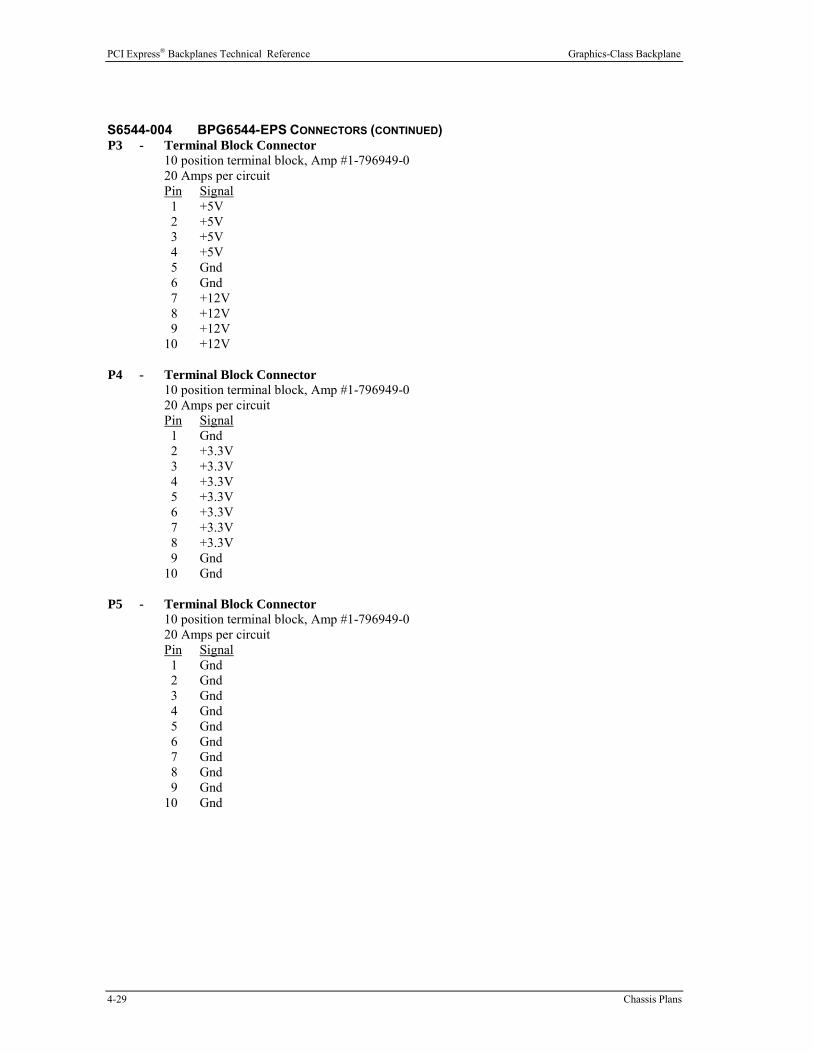
PCI Express® Backplanes Technical Reference Graphics-Class Backplane
4-29 Chassis Plans
S6544-004 BPG6544-EPS CONNECTORS (CONTINUED) P3 - Terminal Block Connector
10 position terminal block, Amp #1-796949-0
20 Amps per circuit
Pin
1
2
3
4
5
6
7
8
9
10
Signal
+5V
+5V
+5V
+5V
Gnd
Gnd
+12V
+12V
+12V
+12V
P4 - Terminal Block Connector 10 position terminal block, Amp #1-796949-0
20 Amps per circuit
Pin
1
2
3
4
5
6
7
8
9
10
Signal
Gnd
+3.3V
+3.3V
+3.3V
+3.3V
+3.3V
+3.3V
+3.3V
Gnd
Gnd
P5 - Terminal Block Connector 10 position terminal block, Amp #1-796949-0
20 Amps per circuit
Pin
1
2
3
4
5
6
7
8
9
10
Signal
Gnd
Gnd
Gnd
Gnd
Gnd
Gnd
Gnd
Gnd
Gnd
Gnd

Graphics-Class Backplane PCI Express® Backplanes Technical Reference
Chassis Plans 4-30
S6544-004 BPG6544-EPS CONNECTORS (CONTINUED) P6 - Power-On Connector
2 pin single row header, Amp #640456-2
Pin
1
2
Signal
PSON#
Gnd
P7 - Power Button Connector 2 pin single row header, Amp #640456-2
Pin
1
2
Signal
PWRBT#
Gnd
P8 - Reset Connector 2 pin single row header, Amp #640456-2
Pin
1
2
P9 -
Signal
SHB_RST#
Gnd
Power Good Connector 2 pin single row header, Amp #640456-2
Pin
1
2
P10 -
Signal
PWRGD
Gnd
I/O Power Connector 20 pin dual row header, Molex #87831-2020
Pin
1
3
5
7
9
11
13
15
17
19
Signal
Gnd
IPMB_DA
IPMB_CL
SMDAT
SMCLK
PWRBT#
Gnd
PWRGD
Gnd
Gnd
Pin
2
4
6
8
10
12
14
16
18
20
Signal
+12V
Gnd
+5V
+5VAUX
+3.3V
PSON#
SHB_RST#
+5VAUX_IN
+5VAUX_IN
-12V

PCI Express® Backplanes Technical Reference Graphics-Class Backplane
4-31 Chassis Plans
S6544-004 BPG6544-EPS CONNECTORS (CONTINUED)
P11 - Universal Serial Bus (USB) Connector 8 pin dual row header, Molex #702-46-0801
(+5V fused with self-resetting fuses)
Pin
1
3
5
7
Signal
+5V-USB0
USB0-
USB0+
Gnd-USB0
Pin
2
4
6
8
P12 -
Signal
+5V-USB1
USB1-
USB1+
Gnd-USB1
Universal Serial Bus (USB) Connector 8 pin dual row header, Molex #702-46-0801
(+5V fused with self-resetting fuses)
Pin
1
3
5
7
Signal
+5V-USB2
USB2-
USB2+
Gnd-USB2
Pin
2
4
6
8
P13 -
Signal
+5V-USB3
USB3-
USB3+
Gnd-USB3
10/100/1000Base-T Ethernet Connector - LAN 0 8 pin shielded RJ-45 connector, Molex #85508-0001
Pin
1
2
3
4
5
6
7
8
Signal
TRP1+
TRP1-
TRP2+
TRP3+
TRP3-
TRP2-
TRP4+
TRP4-
P14 - 10/100/1000Base-T Ethernet Connector - LAN 1 8 pin shielded RJ-45 connector, Molex #85508-0001
Pin
1
2
3
4
5
6
7
8
Signal
TRP1+
TRP1-
TRP2+
TRP3+
TRP3-
TRP2-
TRP4+
TRP4-

Graphics-Class Backplane PCI Express® Backplanes Technical Reference
Chassis Plans 4-32
S6544-004 BPG6544-EPS CONNECTORS (CONTINUED)
P19 - System Management Bus Connector 2 pin single row header, Amp #640456-2
Pin
1
2
Signal
SMB Clock
SMB Data

PCI Express® Backplanes Technical Reference Graphics-Class Backplane
4-33 Chassis Plans
S6600-000 BPG6600 The BPG6600 is a PICMG
® 1.3 compliant, 14-slot form factor, graphics-class backplane made up of a six-
layer .080" thick PCB. The backplane supports Chassis Plans and PICMG®
1.3 14-slot hole patterns.
The backplane has one PCI Express® slot which accepts an SHB Express™
system host board (SHB). It
also has a PCI Express expansion slot (PCIeS) which is a x8 slot that mechanically connects a Chassis
Plans IOB31 I/O expansion board to the backplane, providing an additional x1 PCI Express link from a
graphics-class SHB.
The two remaining PCIe slots provide the mechanical connections between the PCI Express option cards
and either the SHB or the PCIeS slot. The first slot (PCIe1) is a x8 slot which mechanically can support x8,
x4 and x1 PCI Express cards and is driven by a x1 electrical interface from the PCIeS slot. The second slot
(PCIe2) connects to the SHB and provides a x16 PCIe link (A0) between the SHB and the backplane. It is
a x16 slot which mechanically can support x16, x8, x4 and x1 PCI Express cards.
_____________________________________________________________________________________
NOTE: In order to use slot PCIe1 when you are using a Chassis Plans PCI Express SHB, you must have a
Chassis Plans IOB31 (6474-000) I/O expansion board on the SHB. The IOB31 enables communication
between the SHB and slot PCIe1 by providing a x1 PCI Express link to the PCIeS slot.
_____________________________________________________________________________________
The BPG6600 has six PCI-X slots which are connected to the SHB by a x4 PCI Express link (B0) which
drives a PCI Express-to-PCI-X bridge chip, which supports four 64-bit/ 66MHz PCI-X slots and two 64-
bit/100MHz PCI-X slots. The PCI-X slots provide support for PCI-X option cards and PCI option cards,
which must be either +3.3V or universal option cards. If a card has an interface bus speed lower than the
speed of the PCI-X slot in which it is placed, the bridge chip throttles down the bus interface speed to
match that of the card.
NOTE: The 64-bit/66MHz PCI-X slots enable 66MHz PCI-X option cards to run at 66MHz. 66MHz PCI
option cards will function in these slots but may only operate at 33MHz due to the differences between a
PCI and PCI-X bus.
In addition, the BPG6600 supports optional SHB edge connector D, which provides a 32-bit/33MHz PCI
interface to drive four PCI slots, which can accommodate +5V only or universal 32-bit/33MHz PCI option
cards.
The BPG6600 supports the optional Ethernet routing feature of the SHB Express specification and provides
two 10/100/1000Base-T Ethernet RJ-45 connectors. It also has two USB 2.0 headers which are capable of
supporting up to four USB 2.0 ports on the backplane.
USB and Ethernet functionality on the BPG6600 is dependent on the SHB providing I/O capability to edge
connector C of the backplane. In order to take advantage of these I/O features, the SHB in the system must
be able to support the connections as specified in the PCI Industrial Manufacturers Group’s SHB Express™ System Host Board PCI Express Specification, PICMG® 1.3.
The backplane has a power connector (P1) which can accommodate either ATX or EPS power. A +12V
power connector (P2) is provided for routing auxiliary power to the SHB’s edge connectors, eliminating the
need for auxiliary power connections on the system host board. The BPG6600 also has two extended-
current terminal block connectors which provide additional power capacity for power-intensive
applications -- up to 80 Amps of +12V, 80 Amps of +3.3V and 40 Amps of +5V.

Graphics-Class Backplane PCI Express® Backplanes Technical Reference
Chassis Plans 4-34
CAUTION: In some ATX/EPS systems, the power may appear to be off while the +5VSB signal is still
present and supplying power to the SHB, option cards and other system components. The +5VAUX LED
on a Chassis Plans PICMG 1.3 backplane monitors the +5VSB power signal; “green” indicates that the
+5VSB signal is present. Chassis Plans backplane LEDs monitor all DC power signals, and all of the
LEDs should be off before adding or removing components. Removing boards under power may result in
system damage.
Models with other power configurations may be available. Contact Chassis Plans for more information.
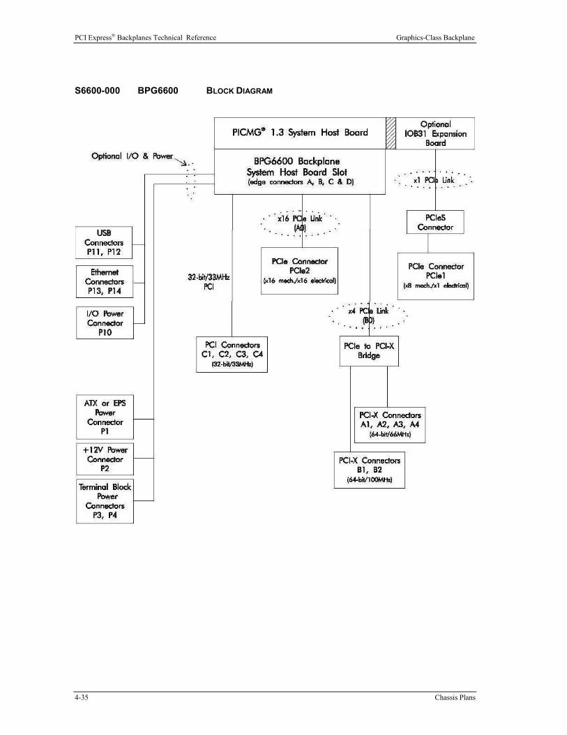
PCI Express® Backplanes Technical Reference Graphics-Class Backplane
4-35 Chassis Plans
S6600-000 BPG6600 BLOCK DIAGRAM

Graphics-Class Backplane PCI Express® Backplanes Technical Reference
Chassis Plans 4-36
S6600-000 BPG6600 DIMENSIONAL DRAWINGS
Chassis Plans 14-Slot Hole Pattern
PCB thickness .080”
Mounting holes .156” diameter
Connector spacing .800” centers

PCI Express® Backplanes Technical Reference Graphics-Class Backplane
4-37 Chassis Plans
S6600-000 BPG6600 DIMENSIONAL DRAWINGS
PICMG® 1.3 14-Slot Hole Pattern
PCB thickness .080”
Mounting holes .156” diameter
Connector spacing .800” centers

Graphics-Class Backplane PCI Express® Backplanes Technical Reference
Chassis Plans 4-38
CONFIGURATION JUMPER The setup of the configuration jumper on the backplane is described below. * indicates the default value of
the jumper.
______________________________________________________________________
NOTE: For the two-position jumper (3-post), “RIGHT” and “LEFT” refer to positioning when the
backplane is viewed with the slots at the top end of the backplane.
______________________________________________________________________
Jumper
JU4
Description
+5V Auxiliary Voltage Install on the LEFT if +5V auxiliary voltage is provided by the
standard +5V supply. This option is used for systems which do
not have either an ATX or EPS standard power input. This
mode provides the necessary +5V for the SHB’s +5VAUX
signal lines. Sleep mode recovery is not supported using non-
ATX/EPS power supplies.
Install on the RIGHT if +5V auxiliary voltage is provided by a
separate +5VAUX signal input pin. This enables the necessary
SHB power signaling and allows recovery from sleep mode.
This option is used for ATX or EPS standard power supplies. *
BPG6600 CONNECTORS
The connectors available on the BPG6600 vary depending on the version of the backplane you have.
Connectors for the S6600-004 (-EPS) and S6600-007 (-CRA) are defined below.
S6600-004 BPG6600-EPS CONNECTORS
NOTE: Pin 1 on the connectors is indicated by the square pad on the PCB.
P1 - ATX/EPS Power Connector 24 pin dual row mini fit JR, Molex #39-29-6248
Pin
1
2
3
4
5
6
7
8
9
10
11
12
Signal
+3.3V
+3.3V
Gnd
+5V
Gnd
+5V
Gnd
PWRGD
+5VAUX
+12V
+12V
+3.3V
Pin
13
14
15
16
17
18
19
20
21
22
23
24
Signal
+3.3V
-12V
Gnd
PSON#
Gnd
Gnd
Gnd
-5V
+5V
+5V
+5V
Gnd

PCI Express® Backplanes Technical Reference Graphics-Class Backplane
4-39 Chassis Plans
S6600-004 BPG6600-EPS CONNECTORS (CONTINUED) P2 - +12V Power Connector
8 pin mini fit JR, Amp #1586037-8
Pin
1
2
3
4
Signal
Gnd
Gnd
Gnd
Gnd
Pin
5
6
7
8
P3 -
Signal
+12V
+12V
+12V
+12V
Terminal Block Connector 10 position terminal block, Amp #1-796949-0
20 Amps per circuit
Pin
1
2
3
4
5
6
7
8
9
10
Signal
+5V
+5V
Gnd
Gnd
Gnd
Gnd
+12V
+12V
+12V
+12V
P4 - Terminal Block Connector 10 position terminal block, Amp #1-796949-0
20 Amps per circuit
Pin
1
2
3
4
5
6
7
8
9
10
Signal
+3.3V
+3.3V
+3.3V
+3.3V
Gnd
Gnd
Gnd
Gnd
Gnd
Gnd
P6 - Power-On Connector 2 pin single row header, Amp #640456-2
Pin
1
2
Signal
PSON#
Gnd

Graphics-Class Backplane PCI Express® Backplanes Technical Reference
Chassis Plans 4-40
S6600-004 BPG6600-EPS CONNECTORS (CONTINUED) P7 - Power Button Connector
2 pin single row header, Amp #640456-2
Pin
1
2
Signal
PWRBT#
Gnd
P8 - Reset Connector 2 pin single row header, Amp #640456-2
Pin
1
2
P9 -
Signal
SHB_RST#
Gnd
Power Good Connector 2 pin single row header, Amp #640456-2
Pin
1
2
P10 -
Signal
PWRGD
Gnd
I/O Power Connector 20 pin dual row header, Molex #87831-2020
Pin
1
3
5
7
9
11
13
15
17
19
Signal
Gnd
IPMB_DA
IPMB_CL
SMDAT
SMCLK
PWRBT#
Gnd
PWRGD
Gnd
Gnd
Pin
2
4
6
8
10
12
14
16
18
20
P11 -
Signal
+12V
Gnd
+5V
+5VAUX
+3.3V
PSON#
SHB_RST#
+5VAUX_IN
+5VAUX_IN
-12V
Universal Serial Bus (USB) Connector 8 pin dual row header, Molex #702-46-0801
(+5V fused with self-resetting fuses)
Pin
1
3
5
7
Signal
+5V-USB0
USB0-
USB0+
Gnd-USB0
Pin
2
4
6
8
Signal
+5V-USB1
USB1-
USB1+
Gnd-USB1

PCI Express® Backplanes Technical Reference Graphics-Class Backplane
4-41 Chassis Plans
S6600-004 BPG6600-EPS CONNECTORS (CONTINUED) P12 - Universal Serial Bus (USB) Connector
8 pin dual row header, Molex #702-46-0801
(+5V fused with self-resetting fuses)
Pin
1
3
5
7
Signal
+5V-USB2
USB2-
USB2+
Gnd-USB2
Pin
2
4
6
8
P13 -
Signal
+5V-USB3
USB3-
USB3+
Gnd-USB3
10/100/1000Base-T Ethernet Connector - LAN 0 8 pin shielded RJ-45 connector, Molex #85508-0001
Pin
1
2
3
4
5
6
7
8
Signal
TRP1+
TRP1-
TRP2+
TRP3+
TRP3-
TRP2-
TRP4+
TRP4-
P14 - 10/100/1000Base-T Ethernet Connector - LAN 1 8 pin shielded RJ-45 connector, Molex #85508-0001
Pin
1
2
3
4
5
6
7
8
Signal
TRP1+
TRP1-
TRP2+
TRP3+
TRP3-
TRP2-
TRP4+
TRP4-
P19 - System Management Bus Connector 2 pin single row header, Amp #640456-2
Pin
1
2
Signal
SMB Clock
SMB Data

Graphics-Class Backplane PCI Express® Backplanes Technical Reference
Chassis Plans 4-42
S6600-007 BPG6600-CRA CONNECTORS
NOTE: Pin 1 on the connectors is indicated by the square pad on the PCB.
P1 - ATX/EPS Power Connector 24 pin right angle dual row mini fit JR, Amp #1-794516-1
Pin
1
2
3
4
5
6
7
8
9
10
11
12
Signal
+3.3V
+3.3V
Gnd
+5V
Gnd
+5V
Gnd
PWRGD
+5VAUX
+12V
+12V
+3.3V
Pin
13
14
15
16
17
18
19
20
21
22
23
24
P2 -
Signal
+3.3V
-12V
Gnd
PSON#
Gnd
Gnd
Gnd
-5V
+5V
+5V
+5V
Gnd
+12V Power Connector 8 pin right angle mini fit JR, Molex #39-30-0080
Pin
1
2
3
4
Signal
Gnd
Gnd
Gnd
Gnd
Pin
5
6
7
8
P3 -
Signal
+12V
+12V
+12V
+12V
Terminal Block Connector 10 position terminal block, Amp #1-796949-0
20 Amps per circuit
Pin
1
2
3
4
5
6
7
8
9
10
Signal
+5V
+5V
Gnd
Gnd
Gnd
Gnd
+12V
+12V
+12V
+12V
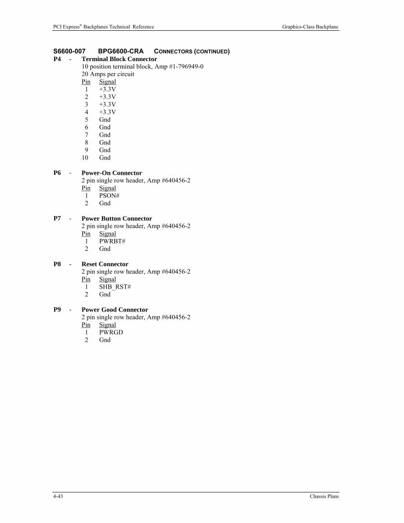
PCI Express® Backplanes Technical Reference Graphics-Class Backplane
4-43 Chassis Plans
S6600-007 BPG6600-CRA CONNECTORS (CONTINUED) P4 - Terminal Block Connector
10 position terminal block, Amp #1-796949-0
20 Amps per circuit
Pin
1
2
3
4
5
6
7
8
9
10
Signal
+3.3V
+3.3V
+3.3V
+3.3V
Gnd
Gnd
Gnd
Gnd
Gnd
Gnd
P6 - Power-On Connector 2 pin single row header, Amp #640456-2
Pin
1
2
Signal
PSON#
Gnd
P7 - Power Button Connector 2 pin single row header, Amp #640456-2
Pin
1
2
Signal
PWRBT#
Gnd
P8 - Reset Connector 2 pin single row header, Amp #640456-2
Pin
1
2
P9 -
Signal
SHB_RST#
Gnd
Power Good Connector 2 pin single row header, Amp #640456-2
Pin
1
2
Signal
PWRGD
Gnd

Graphics-Class Backplane PCI Express® Backplanes Technical Reference
Chassis Plans 4-44
S6600-007 BPG6600-CRA CONNECTORS (CONTINUED) P10 - I/O Power Connector
20 pin dual row header, Molex #87831-2020
Pin
1
3
5
7
9
11
13
15
17
19
Signal
Gnd
IPMB_DA
IPMB_CL
SMDAT
SMCLK
PWRBT#
Gnd
PWRGD
Gnd
Gnd
Pin
2
4
6
8
10
12
14
16
18
20
P11 -
Signal
+12V
Gnd
+5V
+5VAUX
+3.3V
PSON#
SHB_RST#
+5VAUX_IN
+5VAUX_IN
-12V
Universal Serial Bus (USB) Connector 8 pin dual row header, Molex #702-46-0801
(+5V fused with self-resetting fuses)
Pin
1
3
5
7
Signal
+5V-USB0
USB0-
USB0+
Gnd-USB0
Pin
2
4
6
8
P12 -
Signal
+5V-USB1
USB1-
USB1+
Gnd-USB1
Universal Serial Bus (USB) Connector 8 pin dual row header, Molex #702-46-0801
(+5V fused with self-resetting fuses)
Pin
1
3
5
7
Signal
+5V-USB2
USB2-
USB2+
Gnd-USB2
Pin
2
4
6
8
P13 -
Signal
+5V-USB3
USB3-
USB3+
Gnd-USB3
10/100/1000Base-T Ethernet Connector - LAN 0 8 pin shielded RJ-45 connector, Molex #85508-0001
Pin
1
2
3
4
5
6
7
8
Signal
TRP1+
TRP1-
TRP2+
TRP3+
TRP3-
TRP2-
TRP4+
TRP4-

PCI Express® Backplanes Technical Reference Graphics-Class Backplane
4-45 Chassis Plans
S6600-007 BPG6600-CRA CONNECTORS (CONTINUED) P14 - 10/100/1000Base-T Ethernet Connector - LAN 1
8 pin shielded RJ-45 connector, Molex #85508-0001
Pin
1
2
3
4
5
6
7
8
Signal
TRP1+
TRP1-
TRP2+
TRP3+
TRP3-
TRP2-
TRP4+
TRP4-
P19 - System Management Bus Connector 2 pin single row header, Amp #640456-2
Pin
1
2
Signal
SMB Clock
SMB Data

Graphics-Class Backplane PCI Express® Backplanes Technical Reference
Chassis Plans 4-46
S6615-000 BPG6615 The BPG6615 is a graphics-class PICMG-compatible backplane which is a six-layer .080" thick PCB. It is
PICMG®
1.3 compliant and supports Chassis Plans and PICMG®
1.3 14-slot (64-bit) hole patterns.
The backplane has one PCI Express® slot which accepts an SHB Express™
system host board (SHB). It
also has five PCI Express slots (PCIe2 through PCIe6) which provide the mechanical connections between
the PCI Express option cards and the SHB. PCIe2 is a x16 mechanical driven by a x16 PCI Express link
directly from a graphics class SHB and is ideal for high-end graphics cards. It is capable of supporting x16,
x8, x4 and x1 PCI Express option cards. PCIe3 through PCIe6 are x8 mechanical slots and each slot is
deiven by a x4 PCI Express link from the PCI Express fan-out switch. The fan-out switch is driven by a x4
PCI Express link from the graphics-class SHB.
In addition, the BPG6615 has six PCI-X slots. The six PCI-X slots on the BPG6615 are connected to the
SHB via a x4 PCI Express link delivered from the PCI Express fan out switch to the PCI Express-to-PCI-X
bridge chip. The bridge chip provides a 64-bit/66MHz PCI-X channel to support option card slots SLTA1
through SLTA4 and a 64-bit/100MHz PCI-X channel to support slots SLTB1 and SLTB2. These slots
support PCI-X and universal PCI option cards i.e., 5V/3.3V combo or 3.3V only. The bridge chip will
throttle-down the bus interface speeds to match any universal PCI or PCI-X card with an interface bus
speed less than 66MHz or 100MHz.
NOTE: The 64-bit/66MHz PCI-X slots enable 66MHz PCI-X option cards to run at 66MHz. 66MHz PCI
option cards will function in these slots but may only operate at 33MHz due to the differences between a
PCI and PCI-X bus.
The BPG6615 supports the optional Ethernet routing feature of the SHB Express specification and provides
two 10/100/1000Base-T Ethernet RJ-45 connectors. It also has two USB 2.0 headers which are capable of
supporting up to four USB 2.0 ports on the backplane.
USB and Ethernet functionality on the BPG6615 is dependent on the SHB providing I/O capability to edge
connector C of the backplane. In order to take advantage of these I/O features, the SHB in the system must
be able to support the connections as specified in the PCI Industrial Manufacturers Group’s SHB Express™ System Host Board PCI Express Specification, PICMG® 1.3.
The backplane has both right angle and horizontal power connectors which can accommodate either ATX
or EPS power. Two +12V power connectors, right angle and horizontal, are provided for routing auxiliary
power to the SHB’s edge connectors, eliminating the need for auxiliary power connections on the system
host board. The BPG6615 also has two extended-current terminal block connectors which provide
additional power capacity for power-intensive applications -- up to 80 Amps of +12V, 120 Amps of +3.3V
and 80 Amps of +5V.
CAUTION: In some ATX/EPS systems, the power may appear to be off while the +5VSB signal is still
present and supplying power to the SHB, option cards and other system components. The +5VAUX LED
on a Chassis Plans PICMG 1.3 backplane monitors the +5VSB power signal; “green” indicates that the
+5VSB signal is present. Chassis Plans backplane LEDs monitor all DC power signals, and all of the
LEDs should be off before adding or removing components. Removing boards under power may result in
system damage.
Models with other power configurations may be available. Contact Chassis Plans for more information.

PCI Express® Backplanes Technical Reference Graphics-Class Backplane
4-47 Chassis Plans
S6615-000 BPG6615 BLOCK DIAGRAM

Graphics-Class Backplane PCI Express® Backplanes Technical Reference
Chassis Plans 4-48
S6615-000 BPG6615 DIMENSIONAL DRAWING
Chassis Plans Hole Pattern

PCI Express® Backplanes Technical Reference Graphics-Class Backplane
4-49 Chassis Plans
S6615-000 BPG6615 DIMENSIONAL DRAWING
PICMG 1.3 Hole Pattern
*=Pin 1

Graphics-Class Backplane PCI Express® Backplanes Technical Reference
Chassis Plans 4-50
CONFIGURATION JUMPER The setup of the configuration jumper on the backplane is described below. * indicates the default value of
the jumper.
NOTE: For the two-position jumper (3-post), “TOP” and “BOTTOM” refer to positioning when the
backplane is viewed with the slots at the top end of the backplane.
Jumper
JU4
Description
+5V Auxiliary Voltage Install on the TOP if +5V auxiliary voltage is provided by the
standard +5V supply. This option is used for systems which do
not have either an ATX or EPS standard power input. This
mode provides the necessary +5V for the SHB’s +5VAUX
signal lines. Sleep mode recovery is not supported using non-
ATX/EPS power supplies.
Install on the BOTTOM if +5V auxiliary voltage is provided by
a separate +5VAUX signal input pin. This enables the
necessary SHB power signaling and allows recovery from sleep
mode. This option is used for ATX or EPS standard power
supplies. *
S6615-007 BPG6615 CONNECTORS
NOTE: Pin 1 on the connectors is indicated by the square pad on the PCB.
P1 - ATX/EPS Power Connector 24 pin right angle dual row, Molex #39-30-1240
Pin
1
2
3
4
5
6
7
8
9
10
11
12
Signal
+3.3V
+3.3V
Gnd
+5V
Gnd
+5V
Gnd
PWRGD
+5VAUX
+12V
+12V
+3.3V
Pin
13
14
15
16
17
18
19
20
21
22
23
24
P2 -
Signal
+3.3V
-12V
Gnd
PSON#
Gnd
Gnd
Gnd
-5V
+5V
+5V
+5V
Gnd
+12V Power Connector 8 pin right angle dual row, Molex #39-30-0080
Pin
1
2
3
4
Signal
Gnd
Gnd
Gnd
Gnd
Pin
5
6
7
8
Signal
+12V
+12V
+12V
+12V

PCI Express® Backplanes Technical Reference Graphics-Class Backplane
4-51 Chassis Plans
S6615-007 BPG6615 CONNECTORS (CONTINUED) P3 - Terminal Block Connector
10 position terminal block, Phoenix Contract Inc., 19-35-24-2
20 Amps per circuit
Pin
1
2
3
4
5
6
7
8
9
10
P4 -
Signal
+3.3V
+3.3V
+3.3V
+3.3V
Gnd
Gnd
Gnd
Gnd
Gnd
Gnd
Terminal Block Connector 10 position terminal block, Phoenix Contract Inc., 19-35-24-2
20 Amps per circuit
Pin
1
2
3
4
5
6
7
8
9
10
Signal
+5V
+5V
Gnd
Gnd
Gnd
Gnd
Gnd
+12V
+12V
+12V
P6 - Power-On Connector 2 pin single row header, Amp #640456-2
Pin
1
2
Signal
PSON#
Gnd
P7 - Power Button Connector 2 pin single row header, Amp #640456-2
Pin
1
2
Signal
PWRBT#
Gnd
P8 - Reset Connector 2 pin single row header, Amp #640456-2
Pin
1
2
P9 -
Signal
SHB_RST#
Gnd
Power Good Connector 2 pin single row header, Amp #640456-2
Pin
1
2
Signal
PWRGD
Gnd

Graphics-Class Backplane PCI Express® Backplanes Technical Reference
Chassis Plans 4-52
S6615-007 BPG6615 CONNECTORS (CONTINUED) P10 -
I/O Power Connector 20 pin right angle dual row header, Molex
#87833-2020
Pin
1
3
5
7
9
11
13
15
17
19
Signal
Gnd
IPMB_DA
IPMB_CL
SMDAT
SMCLK
PWRBT#
Gnd
PWRGD
GND
GND
Pin
2
4
6
8
10
12
14
16
18
20
P11 -
Signal
+12V
Gnd
+5V
+5VAUX
+3.3V
PSON#
SHB_RST#
5VAUX
5VAUX
-12V
Universal Serial Bus (USB) Connector 8 pin dual row header, Molex #702-46-0801
(+5V fused with self-resetting fuses)
Pin
1
3
5
7
Signal
+5V-USB0
USB0-
USB0+
Gnd-USB0
Pin
2
4
6
8
P12 -
Signal
+5V-USB1
USB1-
USB1+
Gnd-USB1
Universal Serial Bus (USB) Connector 8 pin dual row header, Molex #702-46-0801
(+5V fused with self-resetting fuses)
Pin
1
3
5
7
Signal
+5V-USB2
USB2-
USB2+
Gnd-USB2
Pin
2
4
6
8
P13 -
Signal
+5V-USB3
USB3-
USB3+
Gnd-USB3
10/100/1000Base-T Ethernet Connector - LAN 0 8 pin shielded RJ-45 connector, Molex #43202-8919
Pin
1
2
3
4
5
6
7
8
Signal
TRP1+
TRP1-
TRP2+
TRP3+
TRP3-
TRP2-
TRP4+
TRP4-

PCI Express® Backplanes Technical Reference Graphics-Class Backplane
4-53 Chassis Plans
S6615-007 BPG6615 CONNECTORS (CONTINUED) P14 - 10/100/1000Base-T Ethernet Connector - LAN 1
8 pin shielded RJ-45 connector, Molex #43202-8919
Pin
1
2
3
4
5
6
7
8
Signal
TRP1+
TRP1-
TRP2+
TRP3+
TRP3-
TRP2-
TRP4+
TRP4-
P19 - SMBUS Connector 2 pin single row header, Amp #640456-2
Pin
1
2
P21 -
Signal
SMBUS
Gnd
EPS Power Connector 24 pin vertical dual row, Molex #44206-0007
Pin
1
2
3
4
5
6
7
8
9
10
11
12
Signal
+3.3V
+3.3V
Gnd
+5V
Gnd
+5V
Gnd
PWRGD
+5VAUX
+12V
+12V
+3.3V
Pin
13
14
15
16
17
18
19
20
21
22
23
24
P22 -
Signal
+3.3V
-12V
Gnd
PSON#
Gnd
Gnd
Gnd
-5V
+5V
+5V
+5V
Gnd
+12V Power Connector 8 pin vertical dual row, Molex #44206-0005
Pin
1
2
3
4
Signal
Gnd
Gnd
Gnd
Gnd
Pin
5
6
7
8
Signal
+12V
+12V
+12V
+12V

Graphics-Class Backplane PCI Express® Backplanes Technical Reference
Chassis Plans 4-54
S6714-000 BPG6714 The BPG6714 is a PICMG
® 1.3 compliant, small form factor, graphics-class backplane made up of a six-
layer .062" thick PCB.
The backplane has one PCI Express® slot which accepts an SHB Express™
system host board (SHB). It
also has two PCI Express slots (PCIe1 and PCIe3) which provide the mechanical connections between the
PCI Express option cards and the SHB.
PCIe1 can mechanically support x8, x4 and x1 PCI Exress option cards. PCIe1 uses the PCIe link
provided by the SHB via a Chassis Plans IOB31 I/O expansion board. The IOB31, when attached to a
MCG-series SHB, provides a x4 PCIe link from the SHB to the backplane’s PCIeS slot. A TML or T4L
may also be used. These SHBs will provide a x1 PCI Express link to the BPG6714 backplane’s PCIeS slot
via an IOB31 module.
PCIe3 is a x16 mechanical slot that is driven by a x16PCI Express link (A0) from the SHB. This slot Is
designed to electrically and mechanically support high-end PCI Express graphics and video cards that use a
x16 PCI Express link to communicate to the SHB.
In addition, the BPG6714 has three PCI-X slots (SLTA1, SLTB1 and SLTB2). These are connected to the
SHB via a x4 PCI Express link (B0) via a PCI Express-to-PCI-X bridge chip. The bridge chips support
SLTA1 with a 64-bit/133MHz PCI-X interface and SLTB1 and SLTB2 with a 64-bit/100MHz PCI-X
interface.
The BPG6714 supports the optional Ethernet routing feature of the SHB Express specification and provides
one 10/100/1000Base-T Ethernet RJ-45 connectors. It also has two USB 2.0 headers which are capable of
supporting up to four USB 2.0 ports on the backplane.
NOTE: USB and Ethernet functionality on the BPG6714 is dependent on the SHB providing I/O
capability to edge connector C of the backplane. In order to take advantage of these I/O features, the SHB
in the system must be able to support the connections as specified in the PCI Industrial Manufacturers
Group’s SHB Express™ System Host Board PCI Express Specification, PICMG® 1.3.
The standard BPG6714 backplane is available with a low-profile right-angle power connector sutiable for
use with either an ATX or EPS power supply. An optional BGP6714 is available with straight in or
vertical power connectors. Using straight-in power connectors may interfere with a full-length option card
placed in the SLTB1 slot.
CAUTION: In some ATX/EPS systems, the power may appear to be off while the +5VSB signal is still
present and supplying power to the SHB, option cards and other system components. The +5VAUX LED
on a Chassis Plans PICMG 1.3 backplane monitors the +5VSB power signal; “green” indicates that the
+5VSB signal is present. Chassis Plans backplane LEDs monitor all DC power signals, and all of the
LEDs should be off before adding or removing components. Removing boards under power may result in
system damage.
Models with other power configurations may be available. Contact Chassis Plans for more information.
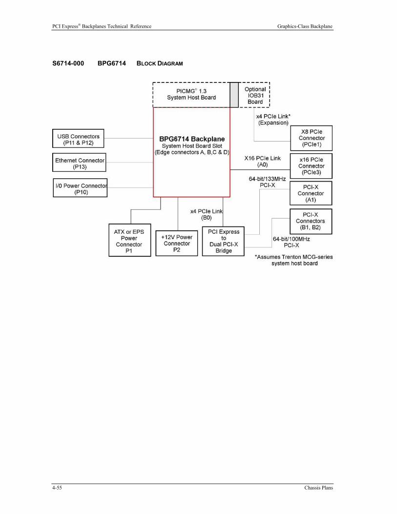
PCI Express® Backplanes Technical Reference Graphics-Class Backplane
4-55 Chassis Plans
S6714-000 BPG6714 BLOCK DIAGRAM

Graphics-Class Backplane PCI Express® Backplanes Technical Reference
Chassis Plans 4-56
S6714-000 BPG6714 DIMENSIONAL DRAWING

PCI Express® Backplanes Technical Reference Graphics-Class Backplane
4-57 Chassis Plans
CONFIGURATION JUMPER The setup of the configuration jumper on the backplane is described below. * indicates the default value of
the jumper.
NOTE: For the two-position jumper (3-post), “RIGHT” and “LEFT” refer to positioning when the
backplane is viewed with the slots at the top end of the backplane.
Jumper
JU4
Description
+5V Auxiliary Voltage Install on the LEFT if +5V auxiliary voltage is provided by the
standard +5V supply. This option is used for systems which do
not have either an ATX or EPS standard power input. This
mode provides the necessary +5V for the SHB’s +5VAUX
signal lines. Sleep mode recovery is not supported using non-
ATX/EPS power supplies.
Install on the RIGHT if +5V auxiliary voltage is provided by a
separate +5VAUX signal input pin. This enables the necessary
SHB power signaling and allows recovery from sleep mode.
This option is used for ATX or EPS standard power supplies. *
S6614-007 BPG6714 CONNECTORS
NOTE: Pin 1 on the connectors is indicated by the square pad on the PCB.
P1 - ATX/EPS Power Connector 24 pin right angle dual row, Molex #39-30-1240
Pin
1
2
3
4
5
6
7
8
9
10
11
12
Signal
+3.3V
+3.3V
Gnd
+5V
Gnd
+5V
Gnd
PWRGD
+5VAUX
+12V
+12V
+3.3V
Pin
13
14
15
16
17
18
19
20
21
22
23
24
Signal
+3.3V
-12V
Gnd
PSON#
Gnd
Gnd
Gnd
-5V
+5V
+5V
+5V
Gnd

Graphics-Class Backplane PCI Express® Backplanes Technical Reference
Chassis Plans 4-58
S6714-007 BPG6714 CONNECTORS (CONTINUED) P2 - +12V Power Connector
8 pin right angle dual row, Molex #39-30-0080
Pin
1
2
3
4
Signal
Gnd
Gnd
Gnd
Gnd
Pin
5
6
7
8
Signal
+12V
+12V
+12V
+12V
P6 - Power-On Connector 2 pin right angle single row header, Molex #22-
05-3021
Pin
1
2
Signal
PSON#
Gnd
P7 - Power Button Connector 2 pin right angle single row header, Molex #22-
05-3021
Pin
1
2
Signal
PWRBT#
Gnd
P8 - Reset Connector 2 pin right angle single row header, Molex #22-
05-3021
Pin
1
2
Signal
SHB_RST#
Gnd
P9 - Power Good Connector 2 pin right angle single row header, Molex #22-
05-3021
Pin
1
2
Signal
PWRGD
Gnd
P10 -
I/O Power Connector 20 pin right angle dual row header, Molex
#87833-2020
Pin
1
3
5
7
9
11
13
15
17
19
Signal
Gnd
IPMB_DA
IPMB_CL
SMDAT
SMCLK
PWRBT#
Gnd
PWRGD
GND
GND
Pin
2
4
6
8
10
12
14
16
18
20
Signal
+12V
Gnd
+5V
+5VAUX
+3.3V
PSON#
SHB_RST#
5VAUX
5VAUX
-12V

PCI Express® Backplanes Technical Reference Graphics-Class Backplane
4-59 Chassis Plans
S6714-007 BPG6714 CONNECTORS (CONTINUED) P11 - Universal Serial Bus (USB) Connector
8 pin dual row header, Molex #702-46-0801
(+5V fused with self-resetting fuses)
Pin
1
3
5
7
Signal
+5V-USB0
USB0-
USB0+
Gnd-USB0
Pin
2
4
6
8
P12 -
Signal
+5V-USB1
USB1-
USB1+
Gnd-USB1
Universal Serial Bus (USB) Connector 8 pin dual row header, Molex #702-46-0801
(+5V fused with self-resetting fuses)
Pin
1
3
5
7
Signal
+5V-USB2
USB2-
USB2+
Gnd-USB2
Pin
2
4
6
8
P13 -
Signal
+5V-USB3
USB3-
USB3+
Gnd-USB3
10/100/1000Base-T Ethernet Connector - LAN 0 8 pin right angle shielded RJ-45 connector, Molex #43202-
8919
Pin
1
2
3
4
5
6
7
8
Signal
TRP1+
TRP1-
TRP2+
TRP3+
TRP3-
TRP2-
TRP4+
TRP4-
P19 - SMBUS Connector 2 pin right angle single row header, Molex #22-
05-3021
Pin
1
2
Signal
SMBUS
Gnd

Graphics-Class Backplane PCI Express® Backplanes Technical Reference
Chassis Plans 4-60
This page intentionally left blank.

PCI Express® Backplanes Technical Reference Server-Class Backplane
5-1 Chassis Plans
Chapter 5 - Server-Class Backplanes
S6377-000 BPX3/8 The BPX3/8 is a PICMG-compatible backplane. It is a six-layer .062" thick PCB which provides three PCI
Express®
slots, four 64-bit/66MHz PCI-X slots and four 64-bit/ 33MHz PCI slots and can support PCI
Express, PCI-X and PCI option cards. The backplane is PICMG®
1.3 compliant and the PCI-to-PCI bridge
supports the PCI Local Bus 2.1 Specification. The backplane supports both Chassis Plans’ modified 14-
slot (64-bit) and PICMG®
1.3 13-slot hole patterns.
Of the three PCI Express slots, one is dedicated to an SHB Express™
system host board (SHB). The two
remaining x16 PCIe slots provide the mechanical connections between the PCI Express option cards and
the SHB. These slots mechanically can support x16, x8, x4 and x1 PCI Express cards. The electrical
interfaces between PCIe slots A1 and B1 and the SHB are x8 PCI Express links.
The four 64-bit/33MHz PCI slots provide support for +5V or universal PCI option cards. The four 64-
bit/66MHz PCI-X slots provide support for PCI option cards and PCI-X option cards, which must be either
+3.3V or universal option cards.
NOTE: The 64-bit/66MHz PCI-X slots enable 66MHz PCI-X option cards to run at 66MHz. 66MHz PCI
option cards will function in these slots but may only operate at 33MHz due to the differences between a
PCI and PCI-X bus.
The BPX3/8 supports the optional Ethernet routing feature of the SHB Express specification and provides
two 10/100/1000Base-T Ethernet RJ-45 connectors. It also has two USB 2.0 headers which are capable of
supporting up to four USB 2.0 ports on the backplane.
USB and Ethernet functionality on the BPX3/8 is dependent on the SHB providing I/O capability to edge
connector C of the backplane. In order to take advantage of these I/O features, the SHB in the system must
be able to support the connections as specified in the PCI Industrial Manufacturers Group’s SHB Express™ System Host Board PCI Express Specification, PICMG® 1.3.
The backplane is available in models which have either ATX or EPS power connections. The ATX model
has standard ATX connectors. The ATX and EPS models have two extended-current terminal block
connectors which provide additional power capacity for power-intensive applications -- up to 80 Amps of
+12V, 80 Amps of +3.3V and 40 Amps of +5V.
Two +12V power connectors are provided on all BPX3/8 models for routing auxiliary power to the SHB’s
edge connectors, eliminating the need for auxiliary power connections on the system host board. These are
8-pin connectors that can accommodate either a 4-pin or 8-pin power cable connection.
CAUTION: Chassis Plans recommends using the EPS model of the backplane in systems using high-
performance, dual-processor SHB Express system host boards. An EPS type of system power supply
provides adequate power delivery in these types of embedded computing systems.

Sever-Class Backplane PCI Express® Backplanes Technical Reference
Chassis Plans 5-2
The power needs of backplane option cards, high-performance processors and other system components
may result in drawing 20A of current from the +12V power supply line. If this occurs, hazardous energy
(240VA) could exist inside the system chassis. Final system/equipment suppliers must provide protection
to service personnel from these potentially hazardous energy levels.
Standby voltages may be used in the final system design to enable certain system recovery operations. In
this case, the power supply may not completely remove power to the system host board when the power
switch is turned off. Caution must be taken to ensure that incoming system power is completely
disconnected before removing the system host board.
Models with other power configurations may be available. Contact Chassis Plans for more information.

PCI Express® Backplanes Technical Reference Server-Class Backplane
5-3 Chassis Plans
S6377-000 BPX3/8 BLOCK DIAGRAM

Sever-Class Backplane PCI Express® Backplanes Technical Reference
Chassis Plans 5-4
S6377-000 BPX3/8 DIMENSIONAL DRAWING
PCI Express® Backplanes Technical Reference Server-Class Backplane
5-5 Chassis Plans
PCB thickness .062”
Mounting holes .156” diameter
Connector spacing .800” centers

Sever-Class Backplane PCI Express® Backplanes Technical Reference
Chassis Plans 5-6
CONFIGURATION JUMPER The setup of the configuration jumper on the backplane is described below. * indicates the default value of
the jumper.
NOTE: For the two-position jumper (3-post), “RIGHT” and “LEFT” refer to positioning when the
backplane is viewed with the slots at the top end of the backplane.
Jumper
JU4
Description
+5V Auxiliary Voltage Install on the LEFT if +5V auxiliary voltage is provided by the
standard +5V supply. This option is used for systems which do
not have either an ATX or EPS standard power input. This
mode provides the necessary +5V for the SHB’s +5VAUX
signal lines. Sleep mode recovery is not supported using non-
ATX/EPS power supplies.
Install on the RIGHT if +5V auxiliary voltage is provided by a
separate +5VAUX signal input pin. This enables the necessary
SHB power signaling and allows recovery from sleep mode.
This option is used for ATX or EPS standard power supplies. *
BPX3/8 CONNECTORS The connectors available on the BPX3/8 vary depending on the version of the backplane you have.
Connectors for the S6377-001 (ATX) and S6377-004 (EPS) tabs are defined below.
S6377-001 BPX3/8-ATX CONNECTORS _
NOTE: Pin 1 on the connectors is indicated by the square pad on the PCB.
P1 - ATX Power Connector 20 pin dual row header, Molex #39-29-9202
Pin
1
2
3
4
5
6
7
8
9
10
Signal
+3.3V
+3.3V
Gnd
+5V
Gnd
+5V
Gnd
PWRGD
+5VAUX
+12V
Pin
11
12
13
14
15
16
17
18
19
20
Signal
+3.3V
-12V
Gnd
PSON#
Gnd
Gnd
Gnd
-5V
+5V
+5V

PCI Express® Backplanes Technical Reference Server-Class Backplane
5-7 Chassis Plans
S6377-001 BPX3/8-ATX CONNECTORS (CONTINUED) P2 - +12V Power Connector
4 pin mini fit JR, Molex #39-29-3046
Pin
1
2
Signal
Gnd
Gnd
Pin
3
4
P3 -
Signal
+12V
+12V
+12V Power Connector 4 pin mini fit JR, Molex #39-29-3046
Pin
1
2
Signal
Gnd
Gnd
Pin
3
4
P4 -
Signal
+12V
+12V
Terminal Block Connector 10 position terminal block, Amp #1-796949-0
20 Amps per circuit
Pin
1
2
3
4
5
6
7
8
9
10
Signal
+3.3V
+3.3V
+5V
Gnd
Gnd
Gnd
Gnd
Gnd
+12V
+12V
P5 - Terminal Block Connector 10 position terminal block, Amp #1-796949-0
20 Amps per circuit
Pin
1
2
3
4
5
6
7
8
9
10
Signal
+3.3V
+3.3V
+5V
Gnd
Gnd
Gnd
Gnd
Gnd
+12V
+12V

Sever-Class Backplane PCI Express® Backplanes Technical Reference
Chassis Plans 5-8
S6377-001 BPX3/8-ATX CONNECTORS (CONTINUED) P6 - Power-On Connector
2 pin single row header, Amp #640456-2
Pin
1
2
Signal
PSON#
Gnd
P7 - Power Button Connector 2 pin single row header, Amp #640456-2
Pin
1
2
Signal
PWRBT#
Gnd
P8 - Reset Connector 2 pin single row header, Amp #640456-2
Pin
1
2
P9 -
Signal
SHB_RST#
Gnd
Power Good Connector 2 pin single row header, Amp #640456-2
Pin
1
2
P10 -
Signal
PWRGD
Gnd
I/O Power Connector 20 pin right angle dual row header, Molex #87833-2020
Pin
1
3
5
7
9
11
13
15
17
19
Signal
Gnd
IPMB_DA
IPMB_CL
SMDAT
SMCLK
PWRBT#
Gnd
PWRGD
NC
NC
Pin
2
4
6
8
10
12
14
16
18
20
Signal
+12V
Gnd
+5V
+5VAUX
+3.3V
PSON#
SHB_RST#
NC
NC
-12V

PCI Express® Backplanes Technical Reference Server-Class Backplane
5-9 Chassis Plans
S6377-001 BPX3/8-ATX CONNECTORS (CONTINUED) P11 - Universal Serial Bus (USB) Connector
8 pin dual row header, Molex #702-46-0801
(+5V fused with self-resetting fuses)
Pin
1
3
5
7
Signal
+5V-USB0
USB0-
USB0+
Gnd-USB0
Pin
2
4
6
8
P12 -
Signal
+5V-USB1
USB1-
USB1+
Gnd-USB1
Universal Serial Bus (USB) Connector 8 pin dual row header, Molex #702-46-0801
(+5V fused with self-resetting fuses)
Pin
1
3
5
7
Signal
+5V-USB2
USB2-
USB2+
Gnd-USB2
Pin
2
4
6
8
P13 -
Signal
+5V-USB3
USB3-
USB3+
Gnd-USB3
10/100/1000Base-T Ethernet Connector - LAN 0 8 pin shielded RA RJ-45 connector, Molex #43202-8110
Pin
1
2
3
4
5
6
7
8
Signal
TRP1+
TRP1-
TRP2+
TRP3+
TRP3-
TRP2-
TRP4+
TRP4-
P14 - 10/100/1000Base-T Ethernet Connector - LAN 1 8 pin shielded RA RJ-45 connector, Molex #43202-8110
Pin
1
2
3
4
5
6
7
8
Signal
TRP1+
TRP1-
TRP2+
TRP3+
TRP3-
TRP2-
TRP4+
TRP4-
Sever-Class Backplane PCI Express® Backplanes Technical Reference
Chassis Plans 5-10
S6377-004 BPX3/8-EPS CONNECTORS
NOTE: Pin 1 on the connectors is indicated by the square pad on the PCB.
P1 - EPS Power Connector 24 pin dual row header, Molex #39-29-9243
Pin
1
2
3
4
5
6
7
8
9
10
11
12
Signal
+3.3V
+3.3V
Gnd
+5V
Gnd
+5V
Gnd
PWRGD
+5VAUX
+12V
+12V
+3.3V
Pin
13
14
15
16
17
18
19
20
21
22
23
24
P2 -
Signal
+3.3V
-12V
Gnd
PSON#
Gnd
Gnd
Gnd
-5V
+5V
+5V
+5V
Gnd
+12V Power Connector 8 pin mini fit JR, Molex #39-29-3086
Pin
1
2
3
4
Signal
Gnd
Gnd
Gnd
Gnd
Pin
5
6
7
8
P3 -
Signal
+12V
+12V
+12V
+12V
+12V Power Connector 8 pin mini fit JR, Molex #39-29-3086
Pin
1
2
3
4
Signal
Gnd
Gnd
Gnd
Gnd
Pin
5
6
7
8
P4 -
Signal
+12V
+12V
+12V
+12V
Terminal Block Connector 10 position terminal block, Amp #1-796949-0
20 Amps per circuit
Pin
1
2
3
4
5
Signal
+3.3V
+3.3V
+5V
Gnd
Gnd

PCI Express® Backplanes Technical Reference Server-Class Backplane
5-11 Chassis Plans
S6377-004 BPX3/8-EPS CONNECTORS (CONTINUED) P4 - Terminal Block Connector (continued) Pin
6
7
8
9
10
Signal
Gnd
Gnd
Gnd
+12V
+12V
P5 - Terminal Block Connector 10 position terminal block, Amp #1-796949-0
20 Amps per circuit
Pin
1
2
3
4
5
6
7
8
9
10
Signal
+3.3V
+3.3V
+5V
Gnd
Gnd
Gnd
Gnd
Gnd
+12V
+12V
P6 - Power-On Connector 2 pin single row header, Amp #640456-2
Pin
1
2
Signal
PSON#
Gnd
P7 - Power Button Connector 2 pin single row header, Amp #640456-2
Pin
1
2
Signal
PWRBT#
Gnd
P8 - Reset Connector 2 pin single row header, Amp #640456-2
Pin
1
2
Signal
SHB_RST#
Gnd

Sever-Class Backplane PCI Express® Backplanes Technical Reference
Chassis Plans 5-12
S6377-004 BPX3/8-EPS CONNECTORS (CONTINUED) P9 - Power Good Connector
2 pin single row header, Amp #640456-2
Pin
1
2
P10 -
Signal
PWRGD
Gnd
I/O Power Connector 20 pin right angle dual row header, Molex #87833-2020
Pin
1
3
5
7
9
11
13
15
17
19
Signal
Gnd
IPMB_DA
IPMB_CL
SMDAT
SMCLK
PWRBT#
Gnd
PWRGD
NC
NC
Pin
2
4
6
8
10
12
14
16
18
20
P11 -
Signal
+12V
Gnd
+5V
+5VAUX
+3.3V
PSON#
SHB_RST#
NC
NC
-12V
Universal Serial Bus (USB) Connector 8 pin dual row header, Molex #702-46-0801
(+5V fused with self-resetting fuses)
Pin
1
3
5
7
Signal
+5V-USB0
USB0-
USB0+
Gnd-USB0
Pin
2
4
6
8
P12 -
Signal
+5V-USB1
USB1-
USB1+
Gnd-USB1
Universal Serial Bus (USB) Connector 8 pin dual row header, Molex #702-46-0801
(+5V fused with self-resetting fuses)
Pin
1
3
5
7
Signal
+5V-USB2
USB2-
USB2+
Gnd-USB2
Pin
2
4
6
8
Signal
+5V-USB3
USB3-
USB3+
Gnd-USB3

PCI Express® Backplanes Technical Reference Server-Class Backplane
5-13 Chassis Plans
S6377-004 BPX3/8-EPS CONNECTORS (CONTINUED) P13 - 10/100/1000Base-T Ethernet Connector - LAN 0
8 pin shielded RA RJ-45 connector, Molex #43202-8110
Pin
1
2
3
4
5
6
7
8
Signal
TRP1+
TRP1-
TRP2+
TRP3+
TRP3-
TRP2-
TRP4+
TRP4-
P14 - 10/100/1000Base-T Ethernet Connector - LAN 1 8 pin shielded RA RJ-45 connector, Molex #43202-8110
Pin
1
2
3
4
5
6
7
8
Signal
TRP1+
TRP1-
TRP2+
TRP3+
TRP3-
TRP2-
TRP4+
TRP4-

Sever-Class Backplane PCI Express® Backplanes Technical Reference
Chassis Plans 5-14
S6467-000 BPX3/14 The BPX3/14 is a PICMG-compatible backplane. It is an eight-layer .080" thick PCB which provides three
PCI Express®
slots, two 64-bit/133MHz PCI-X slots and 12 64-bit/100MHz PCI-X slots and can support
PCI Express, PCI-X and universal PCI option cards. The backplane is PICMG®
1.3 compliant and
supports both Chassis Plans and PICMG®
1.3 20-slot (64-bit) hole patterns. The backplane has mounting
hole inserts recessed approximately .030” into the board’s bottom surface.
One of the PCI Express slots is dedicated to an SHB Express™
system host board (SHB). The BPX3/14
also has a PCI Express expansion slot (PCIeS) which is a x8 slot that mechanically connects a Chassis
Plans IOB31 I/O expansion board to the backplane, providing an additional x4 PCI Express link from a
server-class SHB.
The two remaining PCIe slots provide the mechanical connections between the PCI Express option cards
and either the SHB or the PCIeS slot. The first slot (PCIe1) connects to the SHB and is a x16 slot which
mechanically can support x16, x8, x4 and x1 PCI Express cards. The second slot (PCIe2) connects to the
PCIeS slot and is a x8 slot which mechanically can support x8, x4 and x1 PCI Express cards. The PCI
Express expansion and option card slots use a x4 PCI Express electrical interface.
NOTE: In order to use slot PCIe2 when you are using a Chassis Plans PCI Express SHB, you must have a
Chassis Plans IOB31 (6474-000) I/O expansion board on the SHB. The IOB31 enables communication
between the SHB and slot PCIe2 by providing a x1 or x4 PCI Express link to the PCIeS slot, depending on
the capabilities of the SHB.
The two 64-bit/133MHz PCI-X slots and 12 64-bit/100MHz PCI-X slots provide support for PCI Express,
PCI-X and PCI option cards, which must be either +3.3V or universal option cards.
The BPX3/14 supports the optional Ethernet routing feature of the SHB Express specification and provides
two 10/100/1000Base-T Ethernet RJ-45 connectors. It also has two USB 2.0 headers which are capable of
supporting up to four USB 2.0 ports on the backplane.
USB and Ethernet functionality on the BPX3/14 is dependent on the SHB providing I/O capability to edge
connector C of the backplane. In order to take advantage of these I/O features, the SHB in the system must
be able to support the connections as specified in the PCI Industrial Manufacturers Group’s SHB Express™ System Host Board PCI Express Specification, PICMG® 1.3.
The backplane is available in models which have either ATX or EPS power connections. The ATX model
has standard ATX connectors. The EPS model has three extended- current terminal block connectors
which provide additional power capacity for power- intensive applications -- up to 80 Amps of +12V,
120 Amps of +3.3V and 80 Amps of +5V.
Two +12V power connectors are provided on all BPX3/14 models for routing auxiliary power to the SHB’s
edge connectors, eliminating the need for auxiliary power connections on the system host board. These are
8-pin connectors that can accommodate either a 4-pin or 8-pin power cable connection.

PCI Express® Backplanes Technical Reference Server-Class Backplane
5-15 Chassis Plans
CAUTION: Chassis Plans recommends using the EPS model of the backplane in systems using high-
performance, dual-processor SHB Express system host boards. An EPS type of system power supply
provides adequate power delivery in these types of embedded computing systems.
The power needs of backplane option cards, high-performance processors and other system components
may result in drawing 20A of current from the +12V power supply line. If this occurs, hazardous energy
(240VA) could exist inside the system chassis. Final system/equipment suppliers must provide protection
to service personnel from these potentially hazardous energy levels.
Standby voltages may be used in the final system design to enable certain system recovery operations. In
this case, the power supply may not completely remove power to the system host board when the power
switch is turned off. Caution must be taken to ensure that incoming system power is completely
disconnected before removing the system host board.
Models with other power configurations may be available. Contact Chassis Plans for more information.

Sever-Class Backplane PCI Express® Backplanes Technical Reference
Chassis Plans 5-16
S6467-000 BPX3/14 BLOCK DIAGRAM

PCI Express® Backplanes Technical Reference Server-Class Backplane
5-17 Chassis Plans
S6467-000 BPX3/14 DIMENSIONAL DRAWING
PCB thickness .080”
Mounting holes .156” diameter
Connector spacing .800” centers

Sever-Class Backplane PCI Express® Backplanes Technical Reference
Chassis Plans 5-18
CONFIGURATION JUMPER The setup of the configuration jumper on the backplane is described below. * indicates the default value of
the jumper.
NOTE: For the two-position jumper (3-post), “RIGHT” and “LEFT” refer to positioning when the
backplane is viewed with the slots at the top end of the backplane.
Jumper
JU4
Description
+5V Auxiliary Voltage Install on the LEFT if +5V auxiliary voltage is provided by the
standard +5V supply. This option is used for systems which do
not have either an ATX or EPS standard power input. This
mode provides the necessary +5V for the SHB’s +5VAUX
signal lines. Sleep mode recovery is not supported using non-
ATX/EPS power supplies.
Install on the RIGHT if +5V auxiliary voltage is provided by a
separate +5VAUX signal input pin. This enables the necessary
SHB power signaling and allows recovery from sleep mode.
This option is used for ATX or EPS standard power supplies. *
BPX3/14 CONNECTORS
The connectors available on the BPX3/14 vary depending on the version of the backplane you have.
Connectors for the S6467-001 (ATX) and S6467-004 (EPS) tabs are defined below.
S6467-001 BPX3/14-ATX CONNECTORS
NOTE: Pin 1 on the connectors is indicated by the square pad on the PCB.
P1 - ATX Power Connector 20 pin dual row header, Molex #39-29-9202
Pin
1
2
3
4
5
6
7
8
9
10
Signal
+3.3V
+3.3V
Gnd
+5V
Gnd
+5V
Gnd
PWRGD
+5VAUX
+12V
Pin
11
12
13
14
15
16
17
18
19
20
Signal
+3.3V
-12V
Gnd
PSON#
Gnd
Gnd
Gnd
-5V
+5V
+5V

PCI Express® Backplanes Technical Reference Server-Class Backplane
5-19 Chassis Plans
S6467-001 BPX3/14-ATX CONNECTORS (CONTINUED) P2 - +12V Power Connector
4 pin mini fit JR, Molex #39-29-3046
Pin
1
2
Signal
Gnd
Gnd
Pin
3
4
P3 -
Signal
+12V
+12V
Terminal Block Connector 10 position terminal block, Amp #1-796949-0
20 Amps per circuit
Pin
1
2
3
4
5
6
7
8
9
10
Signal
+5V
+5V
+5V
+5V
Gnd
Gnd
+12V
+12V
+12V
+12V
P4 - Terminal Block Connector 10 position terminal block, Amp #1-796949-0
20 Amps per circuit
Pin
1
2
3
4
5
6
7
8
9
10
Signal
Gnd
Gnd
+3.3V
+3.3V
+3.3V
+3.3V
+3.3V
+3.3V
Gnd
Gnd
P5 - Terminal Block Connector 10 position terminal block, Amp #1-796949-0
20 Amps per circuit
Pin
1
2
3
4
5
Signal
Gnd
Gnd
Gnd
Gnd
Gnd

Sever-Class Backplane PCI Express® Backplanes Technical Reference
Chassis Plans 5-20
S6467-001 BPX3/14-ATX CONNECTORS (CONTINUED) P5 - Terminal Block Connector (continued) Pin
6
7
8
9
10
Signal
Gnd
Gnd
Gnd
Gnd
Gnd
P6 - Power-On Connector 2 pin single row header, Amp #640456-2
Pin
1
2
Signal
PSON#
Gnd
P7 - Power Button Connector 2 pin single row header, Amp #640456-2
Pin
1
2
Signal
PWRBT#
Gnd
P8 - Reset Connector 2 pin single row header, Amp #640456-2
Pin
1
2
P9 -
Signal
External Reset In (Low Active)
Gnd
Power Good Connector 2 pin single row header, Amp #640456-2
Pin
1
2
P10 -
Signal
PWRGD
+3.3V
I/O Power Connector 20 pin right angle dual row header, Molex #87833-2020
Pin
1
3
5
7
9
11
13
Signal
Gnd
IPMB_DA
IPMB_CL
SMDAT
SMCLK
PWRBT#
Gnd
Pin
2
4
6
8
10
12
14
Signal
+12V
Gnd
+5V
+5VAUX_IN
+3.3V
PSON#
SHB_RST#
PCI Express® Backplanes Technical Reference Server-Class Backplane
5-21 Chassis Plans
S6467-001 BPX3/14-ATX CONNECTORS (CONTINUED) P10 - I/O Power Connector (continued) Pin
15
17
19
Signal
PWRGD
Gnd
Gnd
Pin
16
18
20
P11 -
Signal
+5VAUX_IN
+5VAUX_IN
-12V
Universal Serial Bus (USB) Connector 8 pin dual row header, Molex #702-46-0801
(+5V fused with self-resetting fuses)
Pin
1
3
5
7
Signal
+5V-USB0
USB0-
USB0+
Gnd-USB0
Pin
2
4
6
8
P12 -
Signal
+5V-USB1
USB1-
USB1+
Gnd-USB1
Universal Serial Bus (USB) Connector 8 pin dual row header, Molex #702-46-0801
(+5V fused with self-resetting fuses)
Pin
1
3
5
7
Signal
+5V-USB2
USB2-
USB2+
Gnd-USB2
Pin
2
4
6
8
P13 -
Signal
+5V-USB3
USB3-
USB3+
Gnd-USB3
10/100/1000Base-T Ethernet Connector - LAN 0 8 pin shielded RA RJ-45 connector, Molex #43202-8110
Pin
1
2
3
4
5
6
7
8
Signal
TRP1+
TRP1-
TRP2+
TRP3+
TRP3-
TRP2-
TRP4+
TRP4-
P14 - 10/100/1000Base-T Ethernet Connector - LAN 1 8 pin shielded RA RJ-45 connector, Molex #43202-8110
Pin
1
2
3
4
Signal
TRP1+
TRP1-
TRP2+
TRP3+

Sever-Class Backplane PCI Express® Backplanes Technical Reference
Chassis Plans 5-22
S6467-001 BPX3/14-ATX CONNECTORS (CONTINUED) P14 - 10/100/1000Base-T Ethernet Connector - LAN 1 (cont’d) Pin
5
6
7
8
Signal
TRP3-
TRP2-
TRP4+
TRP4-
P19 - System Management Bus Connector 2 pin single row header, Amp #640456-2
Pin
1
2
P21 -
Signal
SMB Clock
SMB Data
ATX Power Connector 20 pin right angle mini fit JR, Molex #35318-2020
Pin
1
2
3
4
5
6
7
8
9
10
Signal
+3.3V
+3.3V
Gnd
+5V
Gnd
+5V
Gnd
PWRGD
+5VAUX
+12V
Pin
11
12
13
14
15
16
17
18
19
20
P22 -
Signal
+3.3V
-12V
Gnd
PSON#
Gnd
Gnd
Gnd
-5V
+5V
+5V
+12V Power Connector 4 pin right angle mini fit JR, Molex #35318-0420
Pin
1
2
Signal
Gnd
Gnd
Pin
3
4
S6467-004 BPX3/14-EPS CONNECTORS
NOTE: Pin 1 on the connectors is indicated by the square pad on the PCB.
Signal
+12V
+12V
P1 - EPS Power Connector 24 pin dual row header, Molex #39-29-9243
Pin
1
2
Signal
+3.3V
+3.3V
Pin
13
14
Signal
+3.3V
-12V

PCI Express® Backplanes Technical Reference Server-Class Backplane
5-23 Chassis Plans
S6467-004 BPX3/14-EPS CONNECTORS (CONTINUED) P1 - EPS Power Connector (continued) Pin
3
4
5
6
7
8
9
10
11
12
Signal
Gnd
+5V
Gnd
+5V
Gnd
PWRGD
+5VAUX
+12V
+12V
+3.3V
Pin
15
16
17
18
19
20
21
22
23
24
P2 -
Signal
Gnd
PSON#
Gnd
Gnd
Gnd
-5V
+5V
+5V
+5V
Gnd
+12V Power Connector 8 pin mini fit JR, Molex #39-29-3086
Pin
1
2
3
4
Signal
Gnd
Gnd
Gnd
Gnd
Pin
5
6
7
8
P3 -
Signal
+12V
+12V
+12V
+12V
Power Supply Connector 10 position terminal block, Amp #1-796949-0
20 Amps per circuit
Pin
1
2
3
4
5
6
7
8
9
10
Signal
+5V
+5V
+5V
+5V
Gnd
Gnd
+12V
+12V
+12V
+12V
P4 - Power Supply Connector 10 position terminal block, Amp #1-796949-0
20 Amps per circuit
Pin
1
2
3
4
5
Signal
Gnd
Gnd
+3.3V
+3.3V
+3.3V
Sever-Class Backplane PCI Express® Backplanes Technical Reference
Chassis Plans 5-24
S6467-004 BPX3/14-EPS CONNECTORS (CONTINUED) P4 - Power Supply Connector (continued) Pin
6
7
8
9
10
Signal
+3.3V
+3.3V
+3.3V
Gnd
Gnd
P5 - Power Supply Connector 10 position terminal block, Amp #1-796949-0
20 Amps per circuit
Pin
1
2
3
4
5
6
7
8
9
10
Signal
Gnd
Gnd
Gnd
Gnd
Gnd
Gnd
Gnd
Gnd
Gnd
Gnd
P6 - Power-On Connector 2 pin single row header, Amp #640456-2
Pin
1
2
Signal
PSON#
Gnd
P7 - Power Button Connector 2 pin single row header, Amp #640456-2
Pin
1
2
Signal
PWRBT#
Gnd
P8 - Reset Connector 2 pin single row header, Amp #640456-2
Pin
1
2
Signal
External Reset In (Low Active)
Gnd

PCI Express® Backplanes Technical Reference Server-Class Backplane
5-25 Chassis Plans
S6467-004 BPX3/14-EPS CONNECTORS (CONTINUED) P9 - Power Good Connector
2 pin single row header, Amp #640456-2
Pin
1
2
P10 -
Signal
PWRGD
+3.3V
I/O Power Connector 20 pin right angle dual row header, Molex #87833-2020
Pin
1
3
5
7
9
11
13
15
17
19
Signal
Gnd
IPMB_DA
IPMB_CL
SMDAT
SMCLK
PWRBT#
Gnd
PWRGD
Gnd
Gnd
Pin
2
4
6
8
10
12
14
16
18
20
P11 -
Signal
+12V
Gnd
+5V
+5VAUX_IN
+3.3V
PSON#
SHB_RST#
+5VAUX_IN
+5VAUX_IN
-12V
Universal Serial Bus (USB) Connector 8 pin dual row header, Molex #702-46-0801
(+5V fused with self-resetting fuses)
Pin
1
3
5
7
Signal
+5V-USB0
USB0-
USB0+
Gnd-USB0
Pin
2
4
6
8
P12 -
Signal
+5V-USB1
USB1-
USB1+
Gnd-USB1
Universal Serial Bus (USB) Connector 8 pin dual row header, Molex #702-46-0801
(+5V fused with self-resetting fuses)
Pin
1
3
5
7
Signal
+5V-USB2
USB2-
USB2+
Gnd-USB2
Pin
2
4
6
8
Signal
+5V-USB3
USB3-
USB3+
Gnd-USB3

Sever-Class Backplane PCI Express® Backplanes Technical Reference
Chassis Plans 5-26
S6467-004 BPX3/14-EPS CONNECTORS (CONTINUED) P13 - 10/100/1000Base-T Ethernet Connector - LAN 0
8 pin shielded RA RJ-45 connector, Molex #43202-8110
Pin
1
2
3
4
5
6
7
8
Signal
TRP1+
TRP1-
TRP2+
TRP3+
TRP3-
TRP2-
TRP4+
TRP4-
P14 - 10/100/1000Base-T Ethernet Connector - LAN 1 8 pin shielded RA RJ-45 connector, Molex #43202-8110
Pin
1
2
3
4
5
6
7
8
Signal
TRP1+
TRP1-
TRP2+
TRP3+
TRP3-
TRP2-
TRP4+
TRP4-
P19 - System Management Bus Connector 2 pin single row header, Amp #640456-2
Pin
1
2
P21 -
Signal
SMB Clock
SMB Data
EPS Power Connector 24 pin right angle dual row header, Amp #794516-1
Pin
1
2
3
4
5
6
7
8
9
10
11
12
Signal
+3.3V
+3.3V
Gnd
+5V
Gnd
+5V
Gnd
PWRGD
+5VAUX
+12V
+12V
+3.3V
Pin
13
14
15
16
17
18
19
20
21
22
23
24
Signal
+3.3V
-12V
Gnd
PSON#
Gnd
Gnd
Gnd
-5V
+5V
+5V
+5V
Gnd

PCI Express® Backplanes Technical Reference Server-Class Backplane
5-27 Chassis Plans
S6467-004 BPX3/14-EPS CONNECTORS (CONTINUED) P22 - +12V Power Connector
8 pin right angle mini fit JR, Molex #39-30-0080
Pin
1
2
3
4
Signal
Gnd
Gnd
Gnd
Gnd
Pin
5
6
7
8
Signal
+12V
+12V
+12V
+12V

Sever-Class Backplane PCI Express® Backplanes Technical Reference
Chassis Plans 5-28
S6510-000 BPX5 The BPX5 is a PICMG
® 1.3 compliant, small form factor, server-class backplane made up of a six-layer
.062" thick PCB.
The backplane has one PCI Express® slot which accepts an SHB Express™
system host board (SHB). It
also has a PCI Express expansion slot (PCIeS) which is a x8 slot that mechanically connects a Chassis
Plans IOB31 I/O expansion board to the backplane, providing an additional x4 PCI Express link from a
server-class SHB.
The four remaining PCIe slots provide the mechanical connections between the PCI Express option cards
and either the SHB or the PCIeS slot. The first slot (PCIe1), which connects to the PCIeS slot, is a x8 slot
which mechanically can support x8, x4 and x1 PCI Express cards. The second slot (PCIe2) connects to the
SHB and provides a x4 PCIe link (B0) between the SHB and the backplane. It is a x8 slot which
mechanically can support x8, x4 and x1 PCI Express cards. Slots PCIe1 and PCIe2 use x4 PCI Express
electrical interfaces.
NOTE: In order to use slot PCIe1 when you are using a Chassis Plans PCI Express SHB, you must have a
Chassis Plans IOB31 (6474-000) I/O expansion board on the SHB. The IOB31 enables communication
between the SHB and slot PCIe1 by providing a x1 or x4 PCI Express link to the PCIeS slot, depending on
the capabilities of the SHB.
PCI Express slots PCIe3 and PCIe4 are driven by two x8 PCI Express links (A0 and A2) from the SHB.
These slots mechanically can support x16, x8, x4 and x1 PCI Express cards.
The BPX5 supports the optional Ethernet routing feature of the SHB Express specification and provides
two 10/100/1000Base-T Ethernet RJ-45 connectors. It also has two USB 2.0 headers which are capable of
supporting up to four USB 2.0 ports on the backplane.
USB and Ethernet functionality on the BPX5 is dependent on the SHB providing I/O capability to edge
connector C of the backplane. In order to take advantage of these I/O features, the SHB in the system must
be able to support the connections as specified in the PCI Industrial Manufacturers Group’s SHB Express™ System Host Board PCI Express Specification, PICMG® 1.3.
The backplane has a power connector (P1) which can accommodate either ATX or EPS power. A +12V
power connector (P2) is provided for routing auxiliary power to the SHB’s edge connectors, eliminating the
need for auxiliary power connections on the system host board.
The BPX5 backplane is available in models which have either right angle or straight-in power connections.
CAUTION: In some ATX/EPS systems, the power may appear to be off while the +5VSB signal is still
present and supplying power to the SHB, option cards and other system components. The +5VAUX LED
on a Chassis Plans PICMG 1.3 backplane monitors the +5VSB power signal; “green” indicates that the
+5VSB signal is present. Chassis Plans backplane LEDs monitor all DC power signals, and all of the
LEDs should be off before adding or removing components. Removing boards under power may result in
system damage.

PCI Express® Backplanes Technical Reference Server-Class Backplane
5-29 Chassis Plans
S6510-000 BPX5 BLOCK DIAGRAM

Sever-Class Backplane PCI Express® Backplanes Technical Reference
Chassis Plans 5-30
S6510-000 BPX5 DIMENSIONAL DRAWING
PCB thickness .062”
Mounting holes .156” diameter
Connector spacing .800” centers

PCI Express® Backplanes Technical Reference Server-Class Backplane
5-31 Chassis Plans
CONFIGURATION JUMPER The setup of the configuration jumper on the backplane is described below. * indicates the default value of
the jumper.
NOTE: For the two-position jumper (3-post), “RIGHT” and “LEFT” refer to positioning when the
backplane is viewed with the slots at the top end of the backplane.
Jumper
JU4
Description
+5V Auxiliary Voltage Install on the LEFT if +5V auxiliary voltage is provided by the
standard +5V supply. This option is used for systems which do
not have either an ATX or EPS standard power input. This
mode provides the necessary +5V for the SHB’s +5VAUX
signal lines. Sleep mode recovery is not supported using non-
ATX/EPS power supplies.
Install on the RIGHT if +5V auxiliary voltage is provided by a
separate +5VAUX signal input pin. This enables the necessary
SHB power signaling and allows recovery from sleep mode.
This option is used for ATX or EPS standard power supplies. *
BPX5 CONNECTORS The connectors available on the BPX5 vary depending on the version of the backplane you have.
Connectors for the S6510-007 (right angle connectors) and S6510-008 (straight- in connectors) are defined
below.
S6510-007 BPX5-CRA CONNECTORS
NOTE: Pin 1 on the connectors is indicated by the square pad on the PCB.
P1 - ATX/EPS Power Connector 24 pin right angle dual row header, Amp #794516-1
Pin
1
2
3
4
5
6
7
8
9
10
11
12
Signal
+3.3V
+3.3V
Gnd
+5V
Gnd
+5V
Gnd
PWRGD
+5VAUX
+12V
+12V
+3.3V
Pin
13
14
15
16
17
18
19
20
21
22
23
24
Signal
+3.3V
-12V
Gnd
PSON#
Gnd
Gnd
Gnd
-5V
+5V
+5V
+5V
Gnd

Sever-Class Backplane PCI Express® Backplanes Technical Reference
Chassis Plans 5-32
S6510-007 BPX5-CRA CONNECTORS (CONTINUED) P2 - +12V Power Connector
8 pin right angle mini fit JR, Molex #39-30-0080
Pin
1
2
3
4
Signal
Gnd
Gnd
Gnd
Gnd
Pin
5
6
7
8
P6 -
Signal
+12V
+12V
+12V
+12V
Power-On Connector 2 pin single row header, Amp #640456-2
Pin
1
2
Signal
PSON#
Gnd
P7 - Power Button Connector 2 pin single row header, Amp #640456-2
Pin
1
2
Signal
PWRBT#
Gnd
P8 - Reset Connector 2 pin single row header, Amp #640456-2
Pin
1
2
P9 -
Signal
SHB_RST#
Gnd
Power Good Connector 2 pin single row header, Amp #640456-2
Pin
1
2
P10 -
Signal
PWRGD
Gnd
I/O Power Connector 20 pin right angle dual row header, Molex #87833-2020
Pin
1
3
5
7
9
11
13
Signal
Gnd
IPMB_DA
IPMB_CL
SMDAT
SMCLK
PWRBT#
Gnd
Pin
2
4
6
8
10
12
14
Signal
+12V
Gnd
+5V
+5VAUX
+3.3V
PSON#
SHB_RST#

PCI Express® Backplanes Technical Reference Server-Class Backplane
5-33 Chassis Plans
S6510-007 BPX5-CRA CONNECTORS (CONTINUED) P10 - I/O Power Connector (continued) Pin
15
17
19
Signal
PWRGD
Gnd
Gnd
Pin
16
18
20
P11 -
Signal
+5VAUX
+5VAUX
-12V
Universal Serial Bus (USB) Connector 8 pin dual row header, Molex #702-46-0801
(+5V fused with self-resetting fuses)
Pin
1
3
5
7
Signal
+5V-USB0
USB0-
USB0+
Gnd-USB0
Pin
2
4
6
8
P12 -
Signal
+5V-USB1
USB1-
USB1+
Gnd-USB1
Universal Serial Bus (USB) Connector 8 pin dual row header, Molex #702-46-0801
(+5V fused with self-resetting fuses)
Pin
1
3
5
7
Signal
+5V-USB2
USB2-
USB2+
Gnd-USB2
Pin
2
4
6
8
P13 -
Signal
+5V-USB3
USB3-
USB3+
Gnd-USB3
10/100/1000Base-T Ethernet Connector - LAN 0 8 pin shielded RA RJ-45 connector, Molex #43202-8919
Pin
1
2
3
4
5
6
7
8
Signal
TRP1+
TRP1-
TRP2+
TRP3+
TRP3-
TRP2-
TRP4+
TRP4-
P14 - 10/100/1000Base-T Ethernet Connector - LAN 1 8 pin shielded RA RJ-45 connector, Molex #43202-8919
Pin
1
2
3
Signal
TRP1+
TRP1-
TRP2+

Sever-Class Backplane PCI Express® Backplanes Technical Reference
Chassis Plans 5-34
S6510-007 BPX5-CRA CONNECTORS (CONTINUED) P14 - 10/100/1000Base-T Ethernet Connector - LAN 1 (cont’d) Pin
4
5
6
7
8
Signal
TRP3+
TRP3-
TRP2-
TRP4+
TRP4-
P19 - System Management Bus Connector 2 pin single row header, Amp #640456-2
Pin
1
2
S6510-008 BPX5-CST CONNECTORS
NOTE: Pin 1 on the connectors is indicated by the square pad on the PCB.
Signal
SMB Clock
SMB Data
P1 - ATX/EPS Power Connector 24 pin dual row mini fit JR, Molex #39-29-6248
Pin
1
2
3
4
5
6
7
8
9
10
11
12
Signal
+3.3V
+3.3V
Gnd
+5V
Gnd
+5V
Gnd
PWRGD
+5VAUX
+12V
+12V
+3.3V
Pin
13
14
15
16
17
18
19
20
21
22
23
24
P2 -
Signal
+3.3V
-12V
Gnd
PSON#
Gnd
Gnd
Gnd
-5V
+5V
+5V
+5V
Gnd
+12V Power Connector 8 pin mini fit JR, Molex #39-29-3086
Pin
1
2
3
4
Signal
Gnd
Gnd
Gnd
Gnd
Pin
5
6
7
8
Signal
+12V
+12V
+12V
+12V

PCI Express® Backplanes Technical Reference Server-Class Backplane
5-35 Chassis Plans
S6510-008 BPX5-CST CONNECTORS (CONTINUED) P6 - Power-On Connector
2 pin single row header, Amp #640456-2
Pin
1
2
Signal
PSON#
Gnd
P7 - Power Button Connector 2 pin single row header, Amp #640456-2
Pin
1
2
Signal
PWRBT#
Gnd
P8 - Reset Connector 2 pin single row header, Amp #640456-2
Pin
1
2
P9 -
Signal
SHB_RST#
Gnd
Power Good Connector 2 pin single row header, Amp #640456-2
Pin
1
2
P10 -
Signal
PWRGD
Gnd
I/O Power Connector 20 pin right angle dual row header, Molex #87833-2020
Pin
1
3
5
7
9
11
13
15
17
19
Signal
Gnd
IPMB_DA
IPMB_CL
SMDAT
SMCLK
PWRBT#
Gnd
PWRGD
Gnd
Gnd
Pin
2
4
6
8
10
12
14
16
18
20
Signal
+12V
Gnd
+5V
+5VAUX
+3.3V
PSON#
SHB_RST#
+5VAUX
+5VAUX
-12V

Sever-Class Backplane PCI Express® Backplanes Technical Reference
Chassis Plans 5-36
S6510-008 BPX5-CST CONNECTORS (CONTINUED) P11 - Universal Serial Bus (USB) Connector
8 pin dual row header, Molex #702-46-0801
(+5V fused with self-resetting fuses)
Pin
1
3
5
7
Signal
+5V-USB0
USB0-
USB0+
Gnd-USB0
Pin
2
4
6
8
P12 -
Signal
+5V-USB1
USB1-
USB1+
Gnd-USB1
Universal Serial Bus (USB) Connector 8 pin dual row header, Molex #702-46-0801
(+5V fused with self-resetting fuses)
Pin
1
3
5
7
Signal
+5V-USB2
USB2-
USB2+
Gnd-USB2
Pin
2
4
6
8
P13 -
Signal
+5V-USB3
USB3-
USB3+
Gnd-USB3
10/100/1000Base-T Ethernet Connector - LAN 0 8 pin shielded RA RJ-45 connector, Molex #43202-8919
Pin
1
2
3
4
5
6
7
8
Signal
TRP1+
TRP1-
TRP2+
TRP3+
TRP3-
TRP2-
TRP4+
TRP4-
P14 - 10/100/1000Base-T Ethernet Connector - LAN 1 8 pin shielded RA RJ-45 connector, Molex #43202-8919
Pin
1
2
3
4
5
6
7
8
Signal
TRP1+
TRP1-
TRP2+
TRP3+
TRP3-
TRP2-
TRP4+
TRP4-

PCI Express® Backplanes Technical Reference Server-Class Backplane
5-37 Chassis Plans
S6510-008 BPX5-CST CONNECTORS (CONTINUED) P19 - System Management Bus Connector
2 pin single row header, Amp #640456-2
Pin
1
2
Signal
SMB Clock
SMB Data

Sever-Class Backplane PCI Express® Backplanes Technical Reference
Chassis Plans 5-38
S6526-000 BPX3/2 The BP3/2 is a PICMG
® 1.3 compliant, small form factor, server-class backplane made up of a six-layer
.062" thick PCB.
The backplane has one PCI Express® slot which accepts an SHB Express™
system host board (SHB). It
also has two x16 PCI Express slots (PCIe1 and PCIe2) which provide the mechanical connections between
the PCI Express option cards and the SHB. These slots are driven by the SHB via two x8 PCI Express
links (A0 and A2) and mechanically can support x16, x8, x4 and x1 PCI Express cards.
In addition, the BPX3/2 has two PCI-X slots (SLTA1 and SLTB1) which are connected to the SHB by a x4
PCI Express link (B0) via a PCI Express-to-PCI-X bridge chip which provides two 64-bit/133MHz PCI-X
channels. The PCI-X slots provide support for PCI-X option cards and PCI option cards, which must be
either +3.3V or universal option cards. If a card with an interface bus speed less than 133MHz is placed in
either of the PCI-X slots, the bridge chip throttles down the bus interface speed to match that of the card.
The BPX3/2 has two USB 2.0 headers which are capable of supporting up to four USB 2.0 ports on the
backplane. USB functionality on the BPX3/2 is dependent on the SHB providing I/O capability to edge
connector C of the backplane. In order to take advantage of the USB capability, the SHB in the system
must be able to support the connections as specified in the PCI Industrial Manufacturers Group’s SHB Express™ System Host Board PCI Express Specification, PICMG® 1.3.
The backplane has a power connector (P1) which can accommodate either ATX or EPS power. A +12V
power connector (P2) is provided for routing auxiliary power to the SHB’s edge connectors, eliminating the
need for auxiliary power connections on the system host board.
The BPX3/2 backplane is available in models which have either right angle or straight-in power
connections.
CAUTION: In some ATX/EPS systems, the power may appear to be off while the +5VSB signal is still
present and supplying power to the SHB, option cards and other system components. The +5VAUX LED
on a Chassis Plans PICMG 1.3 backplane monitors the +5VSB power signal; “green” indicates that the
+5VSB signal is present. Chassis Plans backplane LEDs monitor all DC power signals, and all of the
LEDs should be off before adding or removing components. Removing boards under power may result in
system damage.

PCI Express® Backplanes Technical Reference Server-Class Backplane
5-39 Chassis Plans
S6526-000 BPX3/2 BLOCK DIAGRAM

Sever-Class Backplane PCI Express® Backplanes Technical Reference
Chassis Plans 5-40
S6526-000 BPX3/2 DIMENSIONAL DRAWING
PCB thickness .062”
Mounting holes .156” diameter
Connector spacing .800” centers

PCI Express® Backplanes Technical Reference Server-Class Backplane
5-41 Chassis Plans
CONFIGURATION JUMPER The setup of the configuration jumper on the backplane is described below. * indicates the default value of
the jumper.
NOTE: For the two-position jumper (3-post), “TOP” and “BOTTOM” refer to positioning when the
backplane is viewed with the slots at the top end of the backplane.
Jumper
JU4
Description
+5V Auxiliary Voltage Install on the TOP if +5V auxiliary voltage is provided by the
standard +5V supply. This option is used for systems which do
not have either an ATX or EPS standard power input. This
mode provides the necessary +5V for the SHB’s +5VAUX
signal lines. Sleep mode recovery is not supported using non-
ATX/EPS power supplies.
Install on the BOTTOM if +5V auxiliary voltage is provided by
a separate +5VAUX signal input pin. This enables the
necessary SHB power signaling and allows recovery from sleep
mode. This option is used for ATX or EPS standard power
supplies. *
BPX3/2 CONNECTORS The connectors available on the BPX3/2 vary depending on the version of the backplane you have.
Connectors for the S6526-007 (right angle connectors) and S6526-008 (straight- in connectors) are defined
below.
S6526-007 BPX3/2-CRA CONNECTORS
NOTE: Pin 1 on the connectors is indicated by the square pad on the PCB.
P1 - ATX/EPS Power Connector 24 pin right angle dual row header, Amp #794516-1
Pin
1
2
3
4
5
6
7
8
9
10
11
12
Signal
+3.3V
+3.3V
Gnd
+5V
Gnd
+5V
Gnd
PWRGD
+5VAUX
+12V
+12V
+3.3V
Pin
13
14
15
16
17
18
19
20
21
22
23
24
Signal
+3.3V
-12V
Gnd
PSON#
Gnd
Gnd
Gnd
-5V
+5V
+5V
+5V
Gnd

Sever-Class Backplane PCI Express® Backplanes Technical Reference
Chassis Plans 5-42
S6526-007 BPX3/2-CRA CONNECTORS (CONTINUED) P2 - +12V Power Connector
8 pin right angle mini fit JR, Molex #39-30-0080
Pin
1
2
3
4
Signal
Gnd
Gnd
Gnd
Gnd
Pin
5
6
7
8
P6 -
Signal
+12V
+12V
+12V
+12V
Power-On Connector 2 pin right angle single row header, Molex #22-05-3021
Pin
1
2
Signal
PSON#
Gnd
P7 - Power Button Connector 2 pin right angle single row header, Molex #22-05-3021
Pin
1
2
Signal
PWRBT#
Gnd
P8 - Reset Connector 2 pin right angle single row header, Molex #22-05-3021
Pin
1
2
P9 -
Signal
SHB_RST#
Gnd
Power Good Connector 2 pin right angle single row header, Molex #22-05-3021
Pin
1
2
P10 -
Signal
PWRGD
Gnd
I/O Power Connector 20 pin right angle dual row header, Molex #87833-2020
Pin
1
3
5
7
9
11
13
Signal
Gnd
IPMB_DA
IPMB_CL
SMDAT
SMCLK
PWRBT#
Gnd
Pin
2
4
6
8
10
12
14
Signal
+12V
Gnd
+5V
+5VAUX
+3.3V
PSON#
SHB_RST#

PCI Express® Backplanes Technical Reference Server-Class Backplane
5-43 Chassis Plans
S6526-007 BPX3/2-CRA CONNECTORS (CONTINUED) P10 - I/O Power Connector (continued) Pin
15
17
19
Signal
PWRGD
Gnd
Gnd
Pin
16
18
20
P11 -
Signal
+5VAUX
+5VAUX
-12V
Universal Serial Bus (USB) Connector 8 pin dual row header, Molex #702-46-0801
(+5V fused with self-resetting fuses)
Pin
1
3
5
7
Signal
+5V-USB0
USB0-
USB0+
Gnd-USB0
Pin
2
4
6
8
P12 -
Signal
+5V-USB1
USB1-
USB1+
Gnd-USB1
Universal Serial Bus (USB) Connector 8 pin dual row header, Molex #702-46-0801
(+5V fused with self-resetting fuses)
Pin
1
3
5
7
Signal
+5V-USB2
USB2-
USB2+
Gnd-USB2
Pin
2
4
6
8
P19 -
Signal
+5V-USB3
USB3-
USB3+
Gnd-USB3
System Management Bus Connector 2 pin right angle single row header, Molex #22-05-3021
Pin
1
2
S6526-008 BPX3/2-CST CONNECTORS
NOTE: Pin 1 on the connectors is indicated by the square pad on the PCB.
Signal
SMB Clock
SMB Data
P1 - ATX/EPS Power Connector 24 pin dual row mini fit JR, Molex #39-29-6248
Pin
1
2
3
Signal
+3.3V
+3.3V
Gnd
Pin
13
14
15
Signal
+3.3V
-12V
Gnd

Sever-Class Backplane PCI Express® Backplanes Technical Reference
Chassis Plans 5-44
S6526-008 BPX3/2-CST CONNECTORS (CONTINUED) P1 - ATX/EPS Power Connector (continued) Pin
4
5
6
7
8
9
10
11
12
Signal
+5V
Gnd
+5V
Gnd
PWRGD
+5VAUX
+12V
+12V
+3.3V
Pin
16
17
18
19
20
21
22
23
24
P2 -
Signal
PSON#
Gnd
Gnd
Gnd
-5V
+5V
+5V
+5V
Gnd
+12V Power Connector 8 pin mini fit JR, Molex #39-29-3086
Pin
1
2
3
4
Signal
Gnd
Gnd
Gnd
Gnd
Pin
5
6
7
8
P6 -
Signal
+12V
+12V
+12V
+12V
Power-On Connector 2 pin right angle single row header, Molex #22-05-3021
Pin
1
2
Signal
PSON#
Gnd
P7 - Power Button Connector 2 pin right angle single row header, Molex #22-05-3021
Pin
1
2
Signal
PWRBT#
Gnd
P8 - Reset Connector 2 pin right angle single row header, Molex #22-05-3021
Pin
1
2
P9 -
Signal
SHB_RST#
Gnd
Power Good Connector 2 pin right angle single row header, Molex #22-05-3021
Pin
1
2
Signal
PWRGD
Gnd

PCI Express® Backplanes Technical Reference Server-Class Backplane
5-45 Chassis Plans
S6526-008 BPX3/2-CST CONNECTORS (CONTINUED) P10 - I/O Power Connector
20 pin right angle dual row header, Molex #87833-2020
Pin
1
3
5
7
9
11
13
15
17
19
Signal
Gnd
IPMB_DA
IPMB_CL
SMDAT
SMCLK
PWRBT#
Gnd
PWRGD
Gnd
Gnd
Pin
2
4
6
8
10
12
14
16
18
20
P11 -
Signal
+12V
Gnd
+5V
+5VAUX
+3.3V
PSON#
SHB_RST#
+5VAUX
+5VAUX
-12V
Universal Serial Bus (USB) Connector 8 pin dual row header, Molex #702-46-0801
(+5V fused with self-resetting fuses)
Pin
1
3
5
7
Signal
+5V-USB0
USB0-
USB0+
Gnd-USB0
Pin
2
4
6
8
P12 -
Signal
+5V-USB1
USB1-
USB1+
Gnd-USB1
Universal Serial Bus (USB) Connector 8 pin dual row header, Molex #702-46-0801
(+5V fused with self-resetting fuses)
Pin
1
3
5
7
Signal
+5V-USB2
USB2-
USB2+
Gnd-USB2
Pin
2
4
6
8
P19 -
Signal
+5V-USB3
USB3-
USB3+
Gnd-USB3
System Management Bus Connector 2 pin right angle single row header, Molex #22-05-3021
Pin
1
2
Signal
SMB Clock
SMB Data

Sever-Class Backplane PCI Express® Backplanes Technical Reference
Chassis Plans 5-46
S6571-000 BPX6571 The BPX6571 is a server-class PICMG-compatible backplane which is a six-layer .080" thick PCB. It is
PICMG®
1.3 compliant and supports Chassis Plans and PICMG®
1.3 20-slot (64-bit) hole patterns.
The backplane has one PCI Express® slot which accepts an SHB Express™
system host board (SHB). It
also has two PCI Express slots (PCIe1 and PCIe2) which provide the mechanical connections between the
PCI Express option cards and the SHB. PCI Express slot PCIe1 is a x8 mechanical slot which can support
x8, x4 and x1 PCIe cards and is driven by the SHB via a x4 PCI Express link. PCI Express slot PCIe2 is a
x16 mechanical slot which can support x16, x8, x4 and x1 PCIe cards and is driven by the SHB via a x8
PCI Express link.
In addition, the BPX6571 has sixteen PCI-X slots which are connected to the SHB by two x4 PCI Express
links (A2 and A3) via two PCI Express-to-PCI-X bridge chips, each of which provides two 64-bit/66MHz
PCI-X channels. The PCI-X slots provide support for PCI-X option cards and PCI option cards, which
must be either +3.3V or universal option cards. If a card with an interface bus speed less than 66MHz is
placed in any of the PCI-X slots, the bridge chip throttles down the bus interface speed to match that of the
card.
NOTE: The 64-bit/66MHz PCI-X slots enable 66MHz PCI-X option cards to run at 66MHz. 66MHz PCI
option cards will function in these slots but may only operate at 33MHz due to the differences between a
PCI and PCI-X bus.
The BPX6571 supports the optional Ethernet routing feature of the SHB Express specification and provides
two 10/100/1000Base-T Ethernet RJ-45 connectors. It also has two USB 2.0 headers which are capable of
supporting up to four USB 2.0 ports on the backplane.
USB and Ethernet functionality on the BPX6571 is dependent on the SHB providing I/O capability to edge
connector C of the backplane. In order to take advantage of these I/O features, the SHB in the system must
be able to support the connections as specified in the PCI Industrial Manufacturers Group’s SHB Express™ System Host Board PCI Express Specification, PICMG® 1.3.
The backplane has a power connector (P21) which can accommodate either ATX or EPS power. Two
+12V power connectors (P22 and P23) are provided for routing auxiliary power to the SHB’s edge
connectors, eliminating the need for auxiliary power connections on the system host board. The BPX6571
also has three extended-current terminal block connectors which provide additional power capacity for
power-intensive applications -- up to 80 Amps of +12V, 120 Amps of +3.3V and 80 Amps of +5V.
The BPX6571 backplane is available in models which have either right angle or straight- in power
connections.
CAUTION: In some ATX/EPS systems, the power may appear to be off while the +5VSB signal is still
present and supplying power to the SHB, option cards and other system components. The +5VAUX LED
on a Chassis Plans PICMG 1.3 backplane monitors the +5VSB power signal; “green” indicates that the
+5VSB signal is present. Chassis Plans backplane LEDs monitor all DC power signals, and all of the
LEDs should be off before adding or removing components. Removing boards under power may result in
system damage.
Models with other power configurations may be available. Contact Chassis Plans for more information.

PCI Express® Backplanes Technical Reference Server-Class Backplane
5-47 Chassis Plans
S6571-000 BPX6571 BLOCK DIAGRAM

Sever-Class Backplane PCI Express® Backplanes Technical Reference
Chassis Plans 5-48
S6571-000 BPX6571 DIMENSIONAL DRAWING
PCB thickness .080”
Mounting holes .156” diameter
Connector spacing .800” centers

PCI Express® Backplanes Technical Reference Server-Class Backplane
5-49 Chassis Plans
CONFIGURATION JUMPER The setup of the configuration jumper on the backplane is described below. * indicates the default value of
the jumper.
NOTE: For the two-position jumper (3-post), “RIGHT” and “LEFT” refer to positioning when the
backplane is viewed with the slots at the top end of the backplane.
Jumper
JU4
Description
+5V Auxiliary Voltage Install on the LEFT if +5V auxiliary voltage is provided by the
standard +5V supply. This option is used for systems which do
not have either an ATX or EPS standard power input. This
mode provides the necessary +5V for the SHB’s +5VAUX
signal lines. Sleep mode recovery is not supported using non-
ATX/EPS power supplies.
Install on the RIGHT if +5V auxiliary voltage is provided by a
separate +5VAUX signal input pin. This enables the necessary
SHB power signaling and allows recovery from sleep mode.
This option is used for ATX or EPS standard power supplies. *
BPX6571 CONNECTORS The connectors available on the BPX6571 vary depending on the version of the backplane you have.
Connectors for the S6571-007 (right angle connectors) and S6571- 008 (straight-in connectors) are defined
below.
S6571-007 BPX6571-CRA CONNECTORS
NOTE: Pin 1 on the connectors is indicated by the square pad on the PCB.
P3 - Terminal Block Connector 10 position terminal block, Amp #1-796949-0
20 Amps per circuit
Pin
1
2
3
4
5
6
7
8
9
10
Signal
+3.3V
+3.3V
+5V
Gnd
Gnd
Gnd
Gnd
Gnd
+12V
+12V

Sever-Class Backplane PCI Express® Backplanes Technical Reference
Chassis Plans 5-50
S6571-007 BPX6571-CRA CONNECTORS (CONTINUED) P4 - Terminal Block Connector
10 position terminal block, Amp #1-796949-0
20 Amps per circuit
Pin
1
2
3
4
5
6
7
8
9
10
Signal
+3.3V
+3.3V
+5V
Gnd
Gnd
Gnd
Gnd
Gnd
+12V
+12V
P5 - Terminal Block Connector 10 position terminal block, Amp #1-796949-0
20 Amps per circuit
Pin
1
2
3
4
5
6
7
8
9
10
Signal
+3.3V
+3.3V
+5V
Gnd
Gnd
Gnd
Gnd
Gnd
+12V
+12V
P6 - Power-On Connector 2 pin single row header, Amp #640456-2
Pin
1
2
Signal
PSON#
Gnd
P7 - Power Button Connector 2 pin single row header, Amp #640456-2
Pin
1
2
Signal
PWRBT#
Gnd

PCI Express® Backplanes Technical Reference Server-Class Backplane
5-51 Chassis Plans
S6571-007 BPX6571-CRA CONNECTORS (CONTINUED) P8 - Reset Connector
2 pin single row header, Amp #640456-2
Pin
1
2
P9 -
Signal
SHB_RST#
Gnd
Power Good Connector 2 pin single row header, Amp #640456-2
Pin
1
2
P10 -
Signal
PWRGD
Gnd
I/O Power Connector 20 pin right angle dual row header, Molex #87833-2020
Pin
1
3
5
7
9
11
13
15
17
19
Signal
Gnd
IPMB_DA
IPMB_CL
SMDAT
SMCLK
PWRBT#
Gnd
PWRGD
Gnd
Gnd
Pin
2
4
6
8
10
12
14
16
18
20
P11 -
Signal
+12V
Gnd
+5V
+5VAUX
+3.3V
PSON#
SHB_RST#
+5VAUX_IN
+5VAUX_IN
-12V
Universal Serial Bus (USB) Connector 8 pin dual row header, Molex #702-46-0801
(+5V fused with self-resetting fuses)
Pin
1
3
5
7
Signal
+5V-USB0
USB0-
USB0+
Gnd-USB0
Pin
2
4
6
8
P12 -
Signal
+5V-USB1
USB1-
USB1+
Gnd-USB1
Universal Serial Bus (USB) Connector 8 pin dual row header, Molex #702-46-0801
(+5V fused with self-resetting fuses)
Pin
1
3
5
7
Signal
+5V-USB2
USB2-
USB2+
Gnd-USB2
Pin
2
4
6
8
Signal
+5V-USB3
USB3-
USB3+
Gnd-USB3

Sever-Class Backplane PCI Express® Backplanes Technical Reference
Chassis Plans 5-52
S6571-007 BPX6571-CRA CONNECTORS (CONTINUED) P13 - 10/100/1000Base-T Ethernet Connector - LAN 0
8 pin shielded RA RJ-45 connector, Molex #43860-0025
Pin
1
2
3
4
5
6
7
8
Signal
TRP1+
TRP1-
TRP2+
TRP3+
TRP3-
TRP2-
TRP4+
TRP4-
P14 - 10/100/1000Base-T Ethernet Connector - LAN 1 8 pin shielded RA RJ-45 connector, Molex #43860-0025
Pin
1
2
3
4
5
6
7
8
Signal
TRP1+
TRP1-
TRP2+
TRP3+
TRP3-
TRP2-
TRP4+
TRP4-
P21 - ATX/EPS Power Connector 24 pin right angle dual row header, Amp #794516-1
Pin
1
2
3
4
5
6
7
8
9
10
11
12
Signal
+3.3V
+3.3V
Gnd
+5V
Gnd
+5V
Gnd
PWRGD
+5VAUX
+12V
+12V
+3.3V
Pin
13
14
15
16
17
18
19
20
21
22
23
24
Signal
+3.3V
-12V
Gnd
PSON#
Gnd
Gnd
Gnd
-5V
+5V
+5V
+5V
Gnd

PCI Express® Backplanes Technical Reference Server-Class Backplane
5-53 Chassis Plans
S6571-007 BPX6571-CRA CONNECTORS (CONTINUED) P22 - +12V Power Connector
8 pin right angle mini fit JR, Molex #39-30-0080
Pin
1
2
3
4
Signal
Gnd
Gnd
Gnd
Gnd
Pin
5
6
7
8
P23 -
Signal
+12V
+12V
+12V
+12V
+12V Power Connector 8 pin right angle mini fit JR, Molex #39-30-0080
Pin
1
2
3
4
Signal
Gnd
Gnd
Gnd
Gnd
Pin
5
6
7
8
S6571-008 BPX6571-CST CONNECTORS
NOTE: Pin 1 on the connectors is indicated by the square pad on the PCB.
Signal
+12V
+12V
+12V
+12V
P3 - Terminal Block Connector 10 position terminal block, Amp #1-796949-0
20 Amps per circuit
Pin
1
2
3
4
5
6
7
8
9
10
Signal
+3.3V
+3.3V
+5V
Gnd
Gnd
Gnd
Gnd
Gnd
+12V
+12V
P4 - Terminal Block Connector 10 position terminal block, Amp #1-796949-0
20 Amps per circuit
Pin
1
2
3
4
5
Signal
+3.3V
+3.3V
+5V
Gnd
Gnd

Sever-Class Backplane PCI Express® Backplanes Technical Reference
Chassis Plans 5-54
S6571-008 BPX6571-CST CONNECTORS (CONTINUED) P4 - Terminal Block Connector (continued) Pin
6
7
8
9
10
Signal
Gnd
Gnd
Gnd
+12V
+12V
P5 - Terminal Block Connector 10 position terminal block, Amp #1-796949-0
20 Amps per circuit
Pin
1
2
3
4
5
6
7
8
9
10
Signal
+3.3V
+3.3V
+5V
Gnd
Gnd
Gnd
Gnd
Gnd
+12V
+12V
P6 - Power-On Connector 2 pin single row header, Amp #640456-2
Pin
1
2
Signal
PSON#
Gnd
P7 - Power Button Connector 2 pin single row header, Amp #640456-2
Pin
1
2
Signal
PWRBT#
Gnd
P8 - Reset Connector 2 pin single row header, Amp #640456-2
Pin
1
2
Signal
SHB_RST#
Gnd
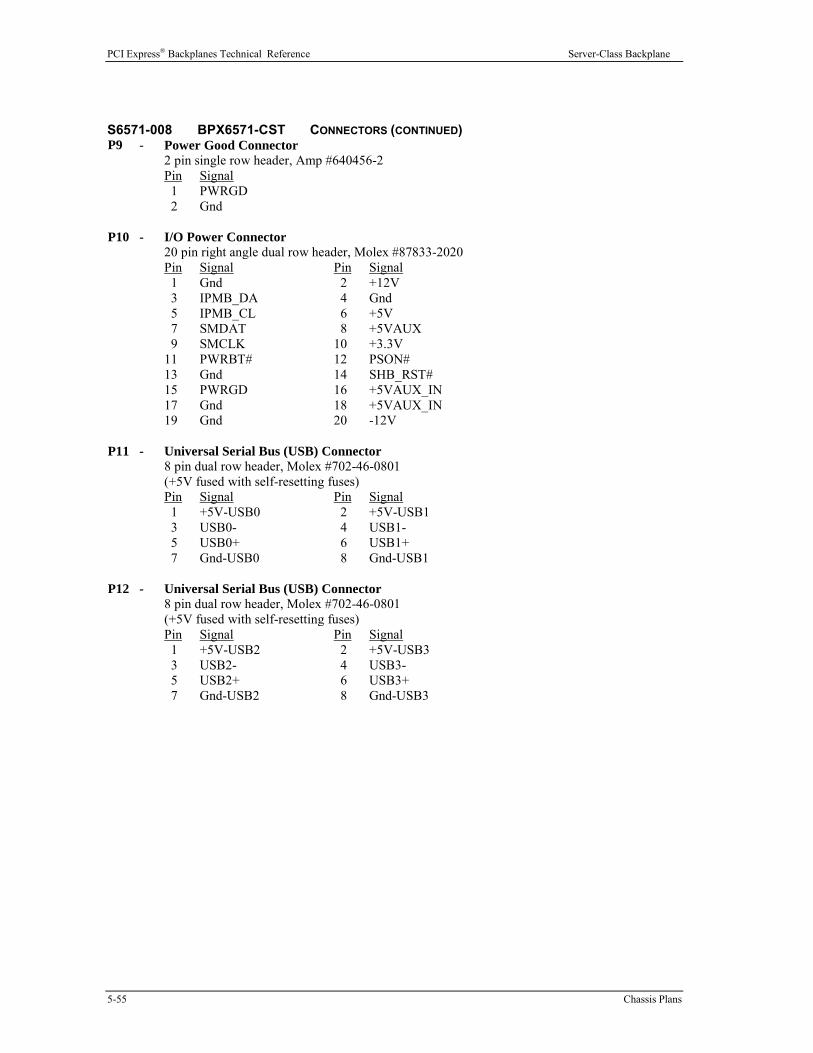
PCI Express® Backplanes Technical Reference Server-Class Backplane
5-55 Chassis Plans
S6571-008 BPX6571-CST CONNECTORS (CONTINUED) P9 - Power Good Connector
2 pin single row header, Amp #640456-2
Pin
1
2
P10 -
Signal
PWRGD
Gnd
I/O Power Connector 20 pin right angle dual row header, Molex #87833-2020
Pin
1
3
5
7
9
11
13
15
17
19
Signal
Gnd
IPMB_DA
IPMB_CL
SMDAT
SMCLK
PWRBT#
Gnd
PWRGD
Gnd
Gnd
Pin
2
4
6
8
10
12
14
16
18
20
P11 -
Signal
+12V
Gnd
+5V
+5VAUX
+3.3V
PSON#
SHB_RST#
+5VAUX_IN
+5VAUX_IN
-12V
Universal Serial Bus (USB) Connector 8 pin dual row header, Molex #702-46-0801
(+5V fused with self-resetting fuses)
Pin
1
3
5
7
Signal
+5V-USB0
USB0-
USB0+
Gnd-USB0
Pin
2
4
6
8
P12 -
Signal
+5V-USB1
USB1-
USB1+
Gnd-USB1
Universal Serial Bus (USB) Connector 8 pin dual row header, Molex #702-46-0801
(+5V fused with self-resetting fuses)
Pin
1
3
5
7
Signal
+5V-USB2
USB2-
USB2+
Gnd-USB2
Pin
2
4
6
8
Signal
+5V-USB3
USB3-
USB3+
Gnd-USB3

Sever-Class Backplane PCI Express® Backplanes Technical Reference
Chassis Plans 5-56
S6571-008 BPX6571-CST CONNECTORS (CONTINUED) P13 - 10/100/1000Base-T Ethernet Connector - LAN 0
8 pin shielded RA RJ-45 connector, Molex #43860-0025
Pin
1
2
3
4
5
6
7
8
Signal
TRP1+
TRP1-
TRP2+
TRP3+
TRP3-
TRP2-
TRP4+
TRP4-
P14 - 10/100/1000Base-T Ethernet Connector - LAN 1 8 pin shielded RA RJ-45 connector, Molex #43860-0025
Pin
1
2
3
4
5
6
7
8
Signal
TRP1+
TRP1-
TRP2+
TRP3+
TRP3-
TRP2-
TRP4+
TRP4-
P21 - ATX/EPS Power Connector 24 pin dual row mini fit JR, Molex #39-29-6248
Pin
1
2
3
4
5
6
7
8
9
10
11
12
Signal
+3.3V
+3.3V
Gnd
+5V
Gnd
+5V
Gnd
PWRGD
+5VAUX
+12V
+12V
+3.3V
Pin
13
14
15
16
17
18
19
20
21
22
23
24
Signal
+3.3V
-12V
Gnd
PSON#
Gnd
Gnd
Gnd
-5V
+5V
+5V
+5V
Gnd
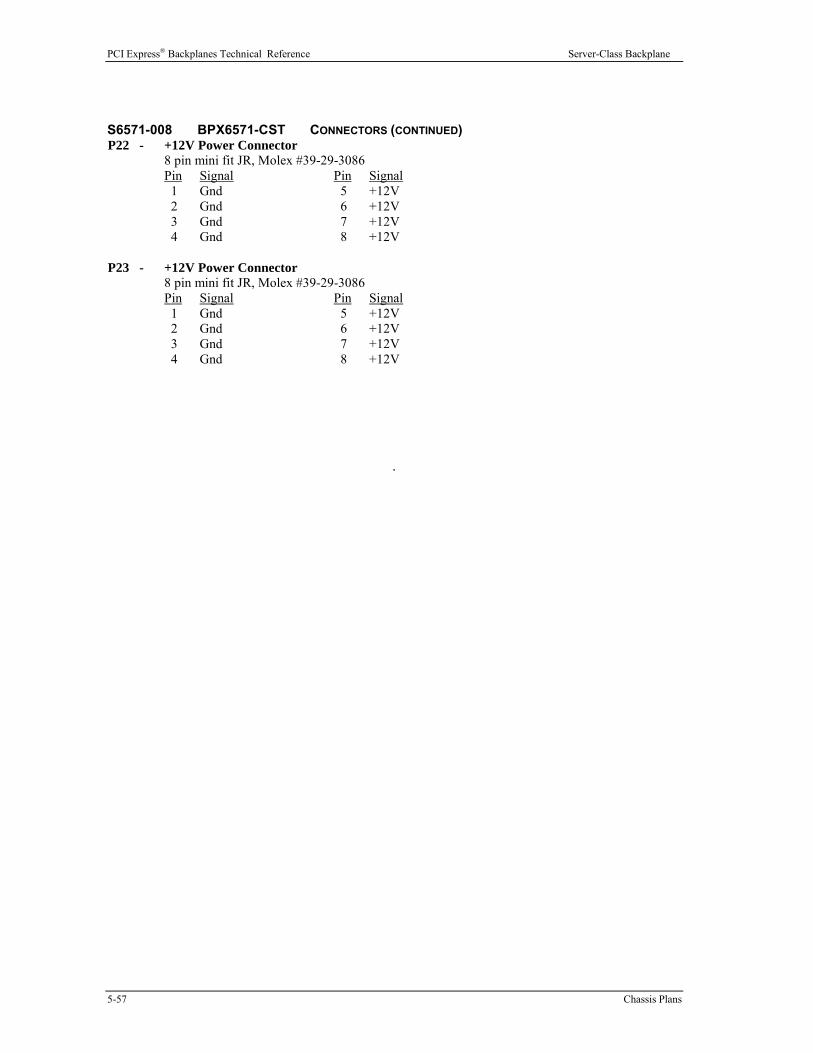
PCI Express® Backplanes Technical Reference Server-Class Backplane
5-57 Chassis Plans
S6571-008 BPX6571-CST CONNECTORS (CONTINUED) P22 - +12V Power Connector
8 pin mini fit JR, Molex #39-29-3086
Pin
1
2
3
4
Signal
Gnd
Gnd
Gnd
Gnd
Pin
5
6
7
8
P23 -
Signal
+12V
+12V
+12V
+12V
+12V Power Connector 8 pin mini fit JR, Molex #39-29-3086
Pin
1
2
3
4
Signal
Gnd
Gnd
Gnd
Gnd
Pin
5
6
7
8
.
Signal
+12V
+12V
+12V
+12V

Sever-Class Backplane PCI Express® Backplanes Technical Reference
Chassis Plans 5-58
S6610-000 BPX6610 The BPX6610 is a server-class PICMG-compatible backplane which is a six-layer .080" thick PCB. It is
PICMG®
1.3 compliant and supports Chassis Plans and PICMG®
1.3 14-slot hole patterns.
The backplane has one PCI Express® slot which accepts an SHB Express™
system host board (SHB). It
also has six PCI Express option card slots (PCIe1 through PCIe6) which provide the mechanical
connections between the PCI Express option cards and the SHB. Option card slots PCIe1 and PCIe2 are
driven by x8 PCI Express links directly from a server-class system host board. PCIe2 is a x16 mechanical
slot capable of supporting x16, x8, x4 or x1 PCI Express option cards. PCIe3 through PCIe6 are x8
mechanical slots and each slot is driven by a x4 PCI Express link from the PCI Express fan out switch. The
fan out switch is driven by a x4 PCI Express link from the server-class SHB.
In addition, the BPX6610 has six PCI-X slots. The six PCI-X slots on the BPX6610 are connected to the
SHB via a x4 PCI Express link delivered from the PCI Express fan out switch to the PCI Express-to-PCI-X
bridge chip. The bridge chip provides a 64-bit/66MHz PCI-X channel to support option card slots SLTA1
through SLTA4 and a 64-bit/100MHz PCI-X channel to support slots SLTB1 and SLTB2. These slots
support PCI-X and universal PCI option cards i.e., 5V/3.3V combo or 3.3V only. The bridge chip will
throttle-down the bus interface speeds to match any universal PCI or PCI-X card with an interface bus
speed less than 66MHz or 100MHz.
NOTE: The 64-bit/66MHz PCI-X slots enable 66MHz PCI-X option cards to run at 66MHz. 66MHz PCI
option cards will function in these slots but may only operate at 33MHz due to the differences between a
PCI and PCI-X bus.
The BPX6610 supports the optional Ethernet routing feature of the SHB Express specification and provides
two 10/100/1000Base-T Ethernet RJ-45 connectors. It also has two USB 2.0 headers which are capable of
supporting up to four USB 2.0 ports on the backplane.
USB and Ethernet functionality on the BPX6610 is dependent on the SHB providing I/O capability to edge
connector C of the backplane. In order to take advantage of these I/O features, the SHB in the system must
be able to support the connections as specified in the PCI Industrial Manufacturers Group’s SHB Express™ System Host Board PCI Express Specification, PICMG® 1.3.
The backplane has both right angle (P1) and horizontal (P21) power connectors which can accommodate
either ATX or EPS power. Two +12V power connectors (P2 – right angle, P22 – horizontal) are provided
for routing auxiliary power to the SHB’s edge connectors, eliminating the need for auxiliary power connec-
tions on the system host board. The BPX6610 also has two extended-current terminal block connectors
which provide additional power capacity for power-intensive applications -- up to 80 Amps of +12V,
120 Amps of +3.3V and 80 Amps of +5V.
CAUTION: In some ATX/EPS systems, the power may appear to be off while the +5VSB signal is still
present and supplying power to the SHB, option cards and other system components. The +5VAUX LED
on a Chassis Plans PICMG 1.3 backplane monitors the +5VSB power signal; “green” indicates that the
+5VSB signal is present. Chassis Plans backplane LEDs monitor all DC power signals, and all of the
LEDs should be off before adding or removing components. Removing boards under power may result in
system damage.
Models with other power configurations may be available. Contact Chassis Plans for more information.

PCI Express® Backplanes Technical Reference Server-Class Backplane
5-59 Chassis Plans
S6610-000 BPX6610 BLOCK DIAGRAM

Sever-Class Backplane PCI Express® Backplanes Technical Reference
Chassis Plans 5-60
S6610-000 BPX6610 DIMENSIONAL DRAWING
Chassis Plans Hole Pattern

PCI Express® Backplanes Technical Reference Server-Class Backplane
5-61 Chassis Plans
S6610-000 BPX6610 DIMENSIONAL DRAWING
PICMG 1.3 Hole Pattern
*=Pin 1

Sever-Class Backplane PCI Express® Backplanes Technical Reference
Chassis Plans 5-62
CONFIGURATION JUMPER The setup of the configuration jumper on the backplane is described below. * indicates the default value of
the jumper.
NOTE: For the two-position jumper (3-post), “TOP” and “BOTTOM” refer to positioning when the
backplane is viewed with the slots at the top end of the backplane.
Jumper
JU4
Description
+5V Auxiliary Voltage Install on the TOP if +5V auxiliary voltage is provided by the
standard +5V supply. This option is used for systems which do
not have either an ATX or EPS standard power input. This
mode provides the necessary +5V for the SHB’s +5VAUX
signal lines. Sleep mode recovery is not supported using non-
ATX/EPS power supplies.
Install on the BOTTOM if +5V auxiliary voltage is provided by
a separate +5VAUX signal input pin. This enables the
necessary SHB power signaling and allows recovery from sleep
mode. This option is used for ATX or EPS standard power
supplies. *
S6610-007 BPX6610 CONNECTORS
NOTE: Pin 1 on the connectors is indicated by the square pad on the PCB.
P1 - ATX/EPS Power Connector 24 pin right angle dual row, Molex #39-30-1240
Pin
1
2
3
4
5
6
7
8
9
10
11
12
Signal
+3.3V
+3.3V
Gnd
+5V
Gnd
+5V
Gnd
PWRGD
+5VAUX
+12V
+12V
+3.3V
Pin
13
14
15
16
17
18
19
20
21
22
23
24
P2 -
Signal
+3.3V
-12V
Gnd
PSON#
Gnd
Gnd
Gnd
-5V
+5V
+5V
+5V
Gnd
+12V Power Connector 8 pin right angle dual row, Molex #39-30-0080
Pin
1
2
3
4
Signal
Gnd
Gnd
Gnd
Gnd
Pin
5
6
7
8
Signal
+12V
+12V
+12V
+12V

PCI Express® Backplanes Technical Reference Server-Class Backplane
5-63 Chassis Plans
S6610-007 BPX6610 CONNECTORS (CONTINUED) P3 - Terminal Block Connector
10 position terminal block, Phoenix Contract Inc., 19-35-24-2
20 Amps per circuit
Pin
1
2
3
4
5
6
7
8
9
10
P4 -
Signal
+3.3V
+3.3V
+3.3V
+3.3V
Gnd
Gnd
Gnd
Gnd
Gnd
Gnd
Terminal Block Connector 10 position terminal block, Phoenix Contract Inc., 19-35-24-2
20 Amps per circuit
Pin
1
2
3
4
5
6
7
8
9
10
Signal
+5V
+5V
Gnd
Gnd
Gnd
Gnd
Gnd
+12V
+12V
+12V
P6 - Power-On Connector 2 pin single row header, Amp #640456-2
Pin
1
2
Signal
PSON#
Gnd
P7 - Power Button Connector 2 pin single row header, Amp #640456-2
Pin
1
2
Signal
PWRBT#
Gnd
P8 - Reset Connector 2 pin single row header, Amp #640456-2
Pin
1
2
P9 -
Signal
SHB_RST#
Gnd
Power Good Connector 2 pin single row header, Amp #640456-2

Sever-Class Backplane PCI Express® Backplanes Technical Reference
Chassis Plans 5-64
S6610-007 BPX6610 CONNECTORS (CONTINUED) P10 -
I/O Power Connector 20 pin right angle dual row header, Molex
#87833-2020
Pin
1
3
5
7
9
11
13
15
17
19
Signal
Gnd
IPMB_DA
IPMB_CL
SMDAT
SMCLK
PWRBT#
Gnd
PWRGD
GND
GND
Pin
2
4
6
8
10
12
14
16
18
20
P11 -
Signal
+12V
Gnd
+5V
+5VAUX
+3.3V
PSON#
SHB_RST#
5VAUX
5VAUX
-12V
Universal Serial Bus (USB) Connector 8 pin dual row header, Molex #702-46-0801
(+5V fused with self-resetting fuses)
Pin
1
3
5
7
Signal
+5V-USB0
USB0-
USB0+
Gnd-USB0
Pin
2
4
6
8
P12 -
Signal
+5V-USB1
USB1-
USB1+
Gnd-USB1
Universal Serial Bus (USB) Connector 8 pin dual row header, Molex #702-46-0801
(+5V fused with self-resetting fuses)
Pin
1
3
5
7
Signal
+5V-USB2
USB2-
USB2+
Gnd-USB2
Pin
2
4
6
8
P13 -
Signal
+5V-USB3
USB3-
USB3+
Gnd-USB3
10/100/1000Base-T Ethernet Connector - LAN 0 8 pin right angle shielded RJ-45 connector, Molex #43202-8919
Pin
1
2
3
4
5
6
7
8
Signal
TRP1+
TRP1-
TRP2+
TRP3+
TRP3-
TRP2-
TRP4+
TRP4-

PCI Express® Backplanes Technical Reference Server-Class Backplane
5-65 Chassis Plans
S6610-007 BPX6610 CONNECTORS (CONTINUED) P14 - 10/100/1000Base-T Ethernet Connector - LAN 1
8 right angle pin shielded RJ-45 connector, Molex #43202-
8919
Pin
1
2
3
4
5
6
7
8
Signal
TRP1+
TRP1-
TRP2+
TRP3+
TRP3-
TRP2-
TRP4+
TRP4-
P19 - SMBUS Connector 2 pin single row header, Amp #640456-2
Pin
1
2
P21 -
Signal
SMBUS
Gnd
EPS Power Connector 24 pin vertical dual row, Molex #44206-0007
Pin
1
2
3
4
5
6
7
8
9
10
11
12
Signal
+3.3V
+3.3V
Gnd
+5V
Gnd
+5V
Gnd
PWRGD
+5VAUX
+12V
+12V
+3.3V
Pin
13
14
15
16
17
18
19
20
21
22
23
24
P22 -
Signal
+3.3V
-12V
Gnd
PSON#
Gnd
Gnd
Gnd
-5V
+5V
+5V
+5V
Gnd
+12V Power Connector 8 pin vertical dual row, Molex #44206-0005
Pin
1
2
3
4
Signal
Gnd
Gnd
Gnd
Gnd
Pin
5
6
7
8
Signal
+12V
+12V
+12V
+12V

Sever-Class Backplane PCI Express® Backplanes Technical Reference
Chassis Plans 5-66
S6620-000 BPX6620 The BPX6620 is a server-class PICMG-compatible backplane which is a six-layer .080" thick PCB. It is
PICMG®
1.3 compliant and supports Chassis Plans and PICMG®
1.3 14-slot (64-bit) hole patterns.
The backplane has one PCI Express® slot which accepts an SHB Express™
system host board (SHB). It
also has a PCI Express expansion slot (PCIeS) which is a x8 slot that mechanically connects a Chassis
Plans IOB31 I/O expansion board to the backplane, providing an additional x4 PCI Express link from a
server-class SHB.
The two remaining PCIe slots provide the mechanical connections between the PCI Express option cards
and either the SHB or the PCIeS slot. The first slot (PCIe1) is a x8 slot which mechanically can support x8,
x4 and x1 PCI Express cards and is driven by a x4 electrical interface from the PCIeS slot. The second slot
(PCIe2) connects to the SHB and provides a x8 PCIe link (A0) between the SHB and the backplane. It is a
x16 slot which mechanically can support x16, x8, x4 and x1 PCI Express cards.
NOTE: In order to use slot PCIe1 when you are using a Chassis Plans PCI Express SHB, you must have a
Chassis Plans IOB31 (6474-000) I/O expansion board on the SHB. The IOB31 enables communication
between the SHB and slot PCIe1 by providing a x4 PCI Express link to the PCIeS slot.
The BPX6620 has a total of ten PCI-X slots which are connected to the SHB by three PCI Express links
(A2, A3 and B0) which drive three PCI Express-to-PCI-X bridge chips. Two of these bridge chips support
four 64-bit/100MHz PCI-X slots each. The third bridge chip supports two 64-bit/133MHz PCI-X slots.
The PCI-X slots provide support for PCI-X option cards and PCI option cards, which must be either +3.3V
or universal option cards. If a card has an interface bus speed lower than the speed of the PCI-X slot in
which it is placed, the bridge chip throttles down the bus interface speed to match that of the card.
The BPX6620 supports the optional Ethernet routing feature of the SHB Express specification and provides
two 10/100/1000Base-T Ethernet RJ-45 connectors. It also has two USB 2.0 headers which are capable of
supporting up to four USB 2.0 ports on the backplane.
USB and Ethernet functionality on the BPX6620 is dependent on the SHB providing I/O capability to edge
connector C of the backplane. In order to take advantage of these I/O features, the SHB in the system must
be able to support the connections as specified in the PCI Industrial Manufacturers Group’s SHB Express™ System Host Board PCI Express Specification, PICMG® 1.3.
The backplane has a power connector (P1) which can accommodate either ATX or EPS power. A +12V
power connector (P2) is provided for routing auxiliary power to the SHB’s edge connectors, eliminating the
need for auxiliary power connections on the system host board. The BPX6620 also has two extended-
current terminal block connectors which provide additional power capacity for power-intensive
applications -- up to 80 Amps of +12V, 80 Amps of +3.3V and 40 Amps of +5V.
CAUTION: In some ATX/EPS systems, the power may appear to be off while the +5VSB signal is still
present and supplying power to the SHB, option cards and other system components. The +5VAUX LED
on a Chassis Plans PICMG 1.3 backplane monitors the +5VSB power signal; “green” indicates that the
+5VSB signal is present. Chassis Plans backplane LEDs monitor all DC power signals, and all of the
LEDs should be off before adding or removing components. Removing boards under power may result in
system damage.
Models with other power configurations may be available. Contact Chassis Plans for more information.
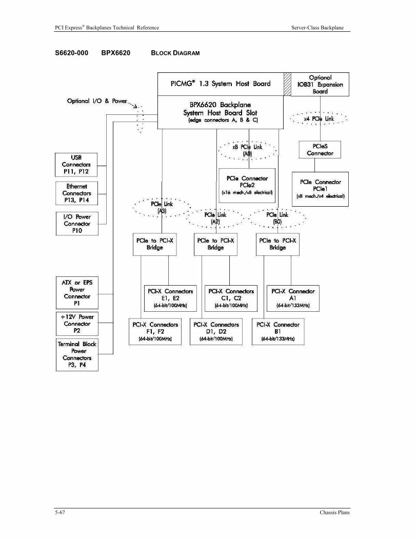
PCI Express® Backplanes Technical Reference Server-Class Backplane
5-67 Chassis Plans
S6620-000 BPX6620 BLOCK DIAGRAM

Sever-Class Backplane PCI Express® Backplanes Technical Reference
Chassis Plans 5-68
S6620-000 BPX6620 DIMENSIONAL DRAWINGS
Chassis Plans 14-Slot Hole Pattern
PCB thickness .080”
Mounting holes .156” diameter
Connector spacing .800” centers

PCI Express® Backplanes Technical Reference Server-Class Backplane
5-69 Chassis Plans
S6620-000 BPX6620 DIMENSIONAL DRAWINGS
PICMG® 1.3 14-Slot Hole Pattern
PCB thickness .080”
Mounting holes .156” diameter
Connector spacing .800” centers

Sever-Class Backplane PCI Express® Backplanes Technical Reference
Chassis Plans 5-70
CONFIGURATION JUMPER The setup of the configuration jumper on the backplane is described below. * indicates the default value of
the jumper.
NOTE: For the two-position jumper (3-post), “TOP” and “BOTTOM” refer to positioning when the
backplane is viewed with the slots at the top end of the backplane.
Jumper
JU4
Description
+5V Auxiliary Voltage Install on the TOP if +5V auxiliary voltage is provided by the
standard +5V supply. This option is used for systems which do
not have either an ATX or EPS standard power input. This
mode provides the necessary +5V for the SHB’s +5VAUX
signal lines. Sleep mode recovery is not supported using non-
ATX/EPS power supplies.
Install on the BOTTOM if +5V auxiliary voltage is provided by
a separate +5VAUX signal input pin. This enables the
necessary SHB power signaling and allows recovery from sleep
mode. This option is used for ATX or EPS standard power
supplies. *
BPX6620 CONNECTORS The connectors available on the BPX6620 vary depending on the version of the backplane you have.
Connectors for the S6620-004 (-EPS) and S6620-007 (-CRA) are defined below.
S6620-004 BPX6620-EPS CONNECTORS
NOTE: Pin 1 on the connectors is indicated by the square pad on the PCB.
P1 - ATX/EPS Power Connector 24 pin dual row header, Molex #44206-0007
Pin
1
2
3
4
5
6
7
8
9
10
11
12
Signal
+3.3V
+3.3V
Gnd
+5V
Gnd
+5V
Gnd
PWRGD
+5VAUX
+12V
+12V
+3.3V
Pin
13
14
15
16
17
18
19
20
21
22
23
24
Signal
+3.3V
-12V
Gnd
PSON#
Gnd
Gnd
Gnd
-5V
+5V
+5V
+5V
Gnd

PCI Express® Backplanes Technical Reference Server-Class Backplane
5-71 Chassis Plans
S6620-004 BPX6620-EPS CONNECTORS (CONTINUED) P2 - +12V Power Connector
8 pin dual row header, Molex #44206-0005
Pin
1
2
3
4
Signal
Gnd
Gnd
Gnd
Gnd
Pin
5
6
7
8
P3 -
Signal
+12V
+12V
+12V
+12V
Terminal Block Connector 10 position terminal block, Amp #1-796949-0
20 Amps per circuit
Pin
1
2
3
4
5
6
7
8
9
10
Signal
+12V
+12V
+12V
+12V
Gnd
Gnd
Gnd
Gnd
+5V
+5V
P4 - Terminal Block Connector 10 position terminal block, Amp #1-796949-0
20 Amps per circuit
Pin
1
2
3
4
5
6
7
8
9
10
Signal
+3.3V
+3.3V
+3.3V
+3.3V
Gnd
Gnd
Gnd
Gnd
Gnd
Gnd
P6 - Power-On Connector 2 pin single row header, Amp #640456-2
Pin
1
2
Signal
PSON#
Gnd

Sever-Class Backplane PCI Express® Backplanes Technical Reference
Chassis Plans 5-72
S6620-004 BPX6620-EPS CONNECTORS (CONTINUED) P7 - Power Button Connector
2 pin single row header, Amp #640456-2
Pin
1
2
Signal
PWRBT#
Gnd
P8 - Reset Connector 2 pin single row header, Amp #640456-2
Pin
1
2
P9 -
Signal
SHB_RST#
Gnd
Power Good Connector 2 pin single row header, Amp #640456-2
Pin
1
2
P10 -
Signal
PWRGD
Gnd
I/O Power Connector 20 pin dual row header, Molex #87831-2020
Pin
1
3
5
7
9
11
13
15
17
19
Signal
Gnd
IPMB_DA
IPMB_CL
SMDAT
SMCLK
PWRBT#
Gnd
PWRGD
Gnd
Gnd
Pin
2
4
6
8
10
12
14
16
18
20
P11 -
Signal
+12V
Gnd
+5V
+5VAUX
+3.3V
PSON#
SHB_RST#
+5VAUX_IN
+5VAUX_IN
-12V
Universal Serial Bus (USB) Connector 8 pin dual row header, Molex #702-46-0801
(+5V fused with self-resetting fuses)
Pin
1
3
5
7
Signal
+5V-USB0
USB0-
USB0+
Gnd-USB0
Pin
2
4
6
8
Signal
+5V-USB1
USB1-
USB1+
Gnd-USB1

PCI Express® Backplanes Technical Reference Server-Class Backplane
5-73 Chassis Plans
S6620-004 BPX6620-EPS CONNECTORS (CONTINUED) P12 - Universal Serial Bus (USB) Connector
8 pin dual row header, Molex #702-46-0801
(+5V fused with self-resetting fuses)
Pin
1
3
5
7
Signal
+5V-USB2
USB2-
USB2+
Gnd-USB2
Pin
2
4
6
8
P13 -
Signal
+5V-USB3
USB3-
USB3+
Gnd-USB3
10/100/1000Base-T Ethernet Connector - LAN 0 8 pin shielded RJ-45 connector, Molex #85508-0001
Pin
1
2
3
4
5
6
7
8
Signal
TRP1+
TRP1-
TRP2+
TRP3+
TRP3-
TRP2-
TRP4+
TRP4-
P14 - 10/100/1000Base-T Ethernet Connector - LAN 1 8 pin shielded RJ-45 connector, Molex #85508-0001
Pin
1
2
3
4
5
6
7
8
Signal
TRP1+
TRP1-
TRP2+
TRP3+
TRP3-
TRP2-
TRP4+
TRP4-
P19 - System Management Bus Connector 2 pin single row header, Amp #640456-2
Pin
1
2
Signal
SMB Clock
SMB Data
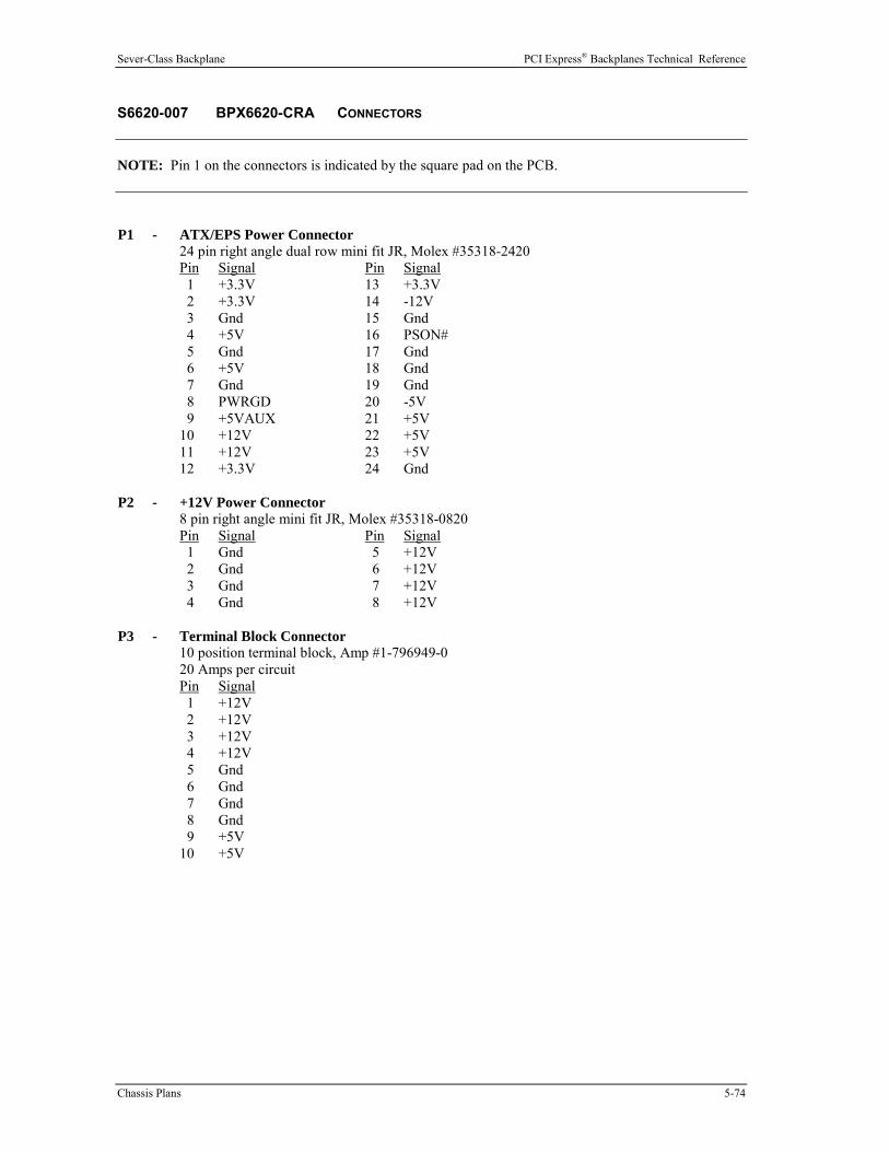
Sever-Class Backplane PCI Express® Backplanes Technical Reference
Chassis Plans 5-74
S6620-007 BPX6620-CRA CONNECTORS
NOTE: Pin 1 on the connectors is indicated by the square pad on the PCB.
P1 - ATX/EPS Power Connector 24 pin right angle dual row mini fit JR, Molex #35318-2420
Pin
1
2
3
4
5
6
7
8
9
10
11
12
Signal
+3.3V
+3.3V
Gnd
+5V
Gnd
+5V
Gnd
PWRGD
+5VAUX
+12V
+12V
+3.3V
Pin
13
14
15
16
17
18
19
20
21
22
23
24
P2 -
Signal
+3.3V
-12V
Gnd
PSON#
Gnd
Gnd
Gnd
-5V
+5V
+5V
+5V
Gnd
+12V Power Connector 8 pin right angle mini fit JR, Molex #35318-0820
Pin
1
2
3
4
Signal
Gnd
Gnd
Gnd
Gnd
Pin
5
6
7
8
P3 -
Signal
+12V
+12V
+12V
+12V
Terminal Block Connector 10 position terminal block, Amp #1-796949-0
20 Amps per circuit
Pin
1
2
3
4
5
6
7
8
9
10
Signal
+12V
+12V
+12V
+12V
Gnd
Gnd
Gnd
Gnd
+5V
+5V

PCI Express® Backplanes Technical Reference Server-Class Backplane
5-75 Chassis Plans
S6620-007 BPX6620-CRA CONNECTORS (CONTINUED) P4 - Terminal Block Connector
10 position terminal block, Amp #1-796949-0
20 Amps per circuit
Pin
1
2
3
4
5
6
7
8
9
10
Signal
+3.3V
+3.3V
+3.3V
+3.3V
Gnd
Gnd
Gnd
Gnd
Gnd
Gnd
P6 - Power-On Connector 2 pin single row header, Amp #640456-2
Pin
1
2
Signal
PSON#
Gnd
P7 - Power Button Connector 2 pin single row header, Amp #640456-2
Pin
1
2
Signal
PWRBT#
Gnd
P8 - Reset Connector 2 pin single row header, Amp #640456-2
Pin
1
2
P9 -
Signal
SHB_RST#
Gnd
Power Good Connector 2 pin single row header, Amp #640456-2
Pin
1
2
Signal
PWRGD
Gnd

Sever-Class Backplane PCI Express® Backplanes Technical Reference
Chassis Plans 5-76
S6620-007 BPX6620-CRA CONNECTORS (CONTINUED) P10 - I/O Power Connector
20 pin dual row header, Molex #87831-2020
Pin
1
3
5
7
9
11
13
15
17
19
Signal
Gnd
IPMB_DA
IPMB_CL
SMDAT
SMCLK
PWRBT#
Gnd
PWRGD
Gnd
Gnd
Pin
2
4
6
8
10
12
14
16
18
20
P11 -
Signal
+12V
Gnd
+5V
+5VAUX
+3.3V
PSON#
SHB_RST#
+5VAUX_IN
+5VAUX_IN
-12V
Universal Serial Bus (USB) Connector 8 pin dual row header, Molex #702-46-0801
(+5V fused with self-resetting fuses)
Pin
1
3
5
7
Signal
+5V-USB0
USB0-
USB0+
Gnd-USB0
Pin
2
4
6
8
P12 -
Signal
+5V-USB1
USB1-
USB1+
Gnd-USB1
Universal Serial Bus (USB) Connector 8 pin dual row header, Molex #702-46-0801
(+5V fused with self-resetting fuses)
Pin
1
3
5
7
Signal
+5V-USB2
USB2-
USB2+
Gnd-USB2
Pin
2
4
6
8
P13 -
Signal
+5V-USB3
USB3-
USB3+
Gnd-USB3
10/100/1000Base-T Ethernet Connector - LAN 0 8 pin shielded RJ-45 connector, Molex #85508-0001
Pin
1
2
3
4
5
6
7
8
Signal
TRP1+
TRP1-
TRP2+
TRP3+
TRP3-
TRP2-
TRP4+
TRP4-

PCI Express® Backplanes Technical Reference Server-Class Backplane
5-77 Chassis Plans
S6620-007 BPX6620-CRA CONNECTORS (CONTINUED) P14 - 10/100/1000Base-T Ethernet Connector - LAN 1
8 pin shielded RJ-45 connector, Molex #85508-0001
Pin
1
2
3
4
5
6
7
8
Signal
TRP1+
TRP1-
TRP2+
TRP3+
TRP3-
TRP2-
TRP4+
TRP4-
P19 - System Management Bus Connector 2 pin single row header, Amp #640456-2
Pin
1
2
Signal
SMB Clock
SMB Data

Sever-Class Backplane PCI Express® Backplanes Technical Reference
Chassis Plans 5-78
S6719-000 BPX6719 The BPX6719 is a PICMG
® 1.3 compliant , small form factor, server-class backplane made up of a six-
layer .062" thick PCB.
The backplane has one PCI Express® slot which accepts an SHB Express™
system host board (SHB). It
also has three PCI Express slots (PCIe1 through PCIe3) which provide the mechanical connections between
the PCI Express option cards and the SHB.
Two PCI Express slots (slots PCIe1 and PCIe2) on the BPX6719 are x8 slots that mechanically support x8,
x4 and x1 PCI Express cards. PCI Express option card slot PCIe2 is driven directly by the SHB via a x8
PCI Express link (A2) from the server-class SHB and PCIe1 uses the x4 PCIe link provided by the SHB via
a Chassis Plans IOB31 I/O expansion board. The IOB31 is attached to the SHB and connects to the
backplane's PCIeS slot.
PCIe3 is a x16 PCI Express mechanical slot that is driven by a x8 PCI Express link (A0) from the SHB.
This slot mechanically supports x16, x8, x4 and x1 PCI Express option cards.
Three PCI-X slots (SLTA1, SLTB1 and SLTB2) on the BPX6719 are connected to the SHB via a x4 PCI
Express link (B0) via a PCI Express-to-PCI-X bridge chip. The bridge chip supports SLTA1 with a 64-
bit/133MHz PCI-X interface and SLTB1 and SLTB2 with a 64-bit/100MHz PCI-X interface. These slots
support PCI-X and universal PCI option cards, (i.e. 5V/3.3V combo or 3.3V only).
The BPX6719 supports the optional Ethernet routing feature of the SHB Express specification and provides
one 10/100/1000Base-T Ethernet RJ-45 connectors. It also has two USB 2.0 headers which are capable of
supporting up to four USB 2.0 ports on the backplane.
USB and Ethernet functionality on the BPX6719 is dependent on the SHB providing I/O capability to edge
connector C of the backplane. In order to take advantage of these I/O features, the SHB in the system must
be able to support the connections as specified in the PCI Industrial Manufacturers Group’s SHB Express™ System Host Board PCI Express Specification, PICMG® 1.3.
The standard BPX6719 backplane is available with a low-profile right-angle power connector suitable for
use with either an ATX or EPS power supply. An optional BPX 6719 is available with straight in or
vertical power connectors. Using straight-in power connectors may interfere with a full-length option card
placed in the SLTB1 slot.
______________________________________________________________________
CAUTION: In some ATX/EPS systems, the power may appear to be off while the +5VSB signal is still
present and supplying power to the SHB, option cards and other system components. The +5VAUX LED
on a Chassis Plans PICMG 1.3 backplane monitors the +5VSB power signal; “green” indicates that the
+5VSB signal is present. Chassis Plans backplane LEDs monitor all DC power signals, and all of the
LEDs should be off before adding or removing components. Removing boards under power may result in
system damage.
______________________________________________________________________
Models with other power configurations may be available. Contact Chassis Plans’ for more information.
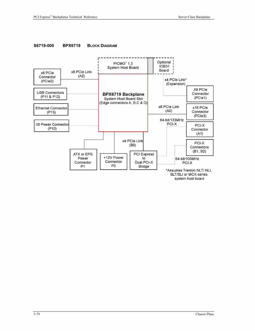
PCI Express® Backplanes Technical Reference Server-Class Backplane
5-79 Chassis Plans
S6719-000 BPX6719 BLOCK DIAGRAM
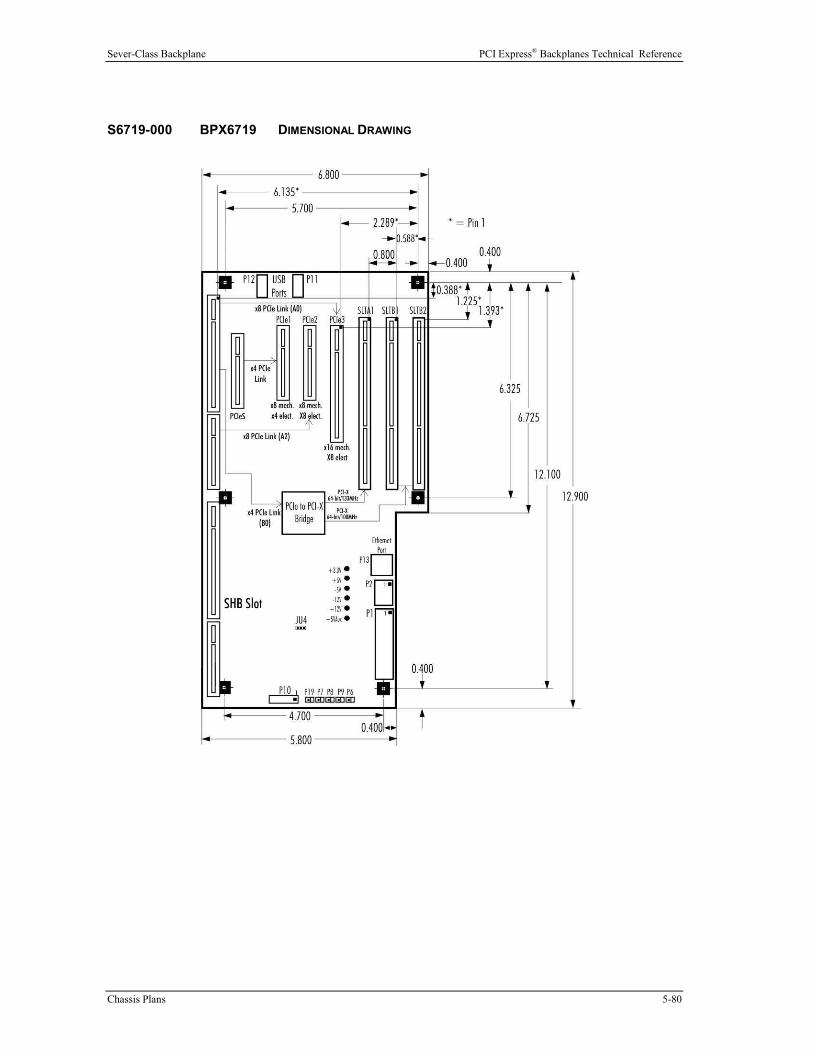
Sever-Class Backplane PCI Express® Backplanes Technical Reference
Chassis Plans 5-80
S6719-000 BPX6719 DIMENSIONAL DRAWING

PCI Express® Backplanes Technical Reference Server-Class Backplane
5-81 Chassis Plans
CONFIGURATION JUMPER The setup of the configuration jumper on the backplane is described below. * indicates the default value of
the jumper.
NOTE: For the two-position jumper (3-post), “RIGHT” and “LEFT” refer to positioning when the
backplane is viewed with the slots at the top end of the backplane.
Jumper
JU4
Description
+5V Auxiliary Voltage Install on the LEFT if +5V auxiliary voltage is provided by the
standard +5V supply. This option is used for systems which do
not have either an ATX or EPS standard power input. This
mode provides the necessary +5V for the SHB’s +5VAUX
signal lines. Sleep mode recovery is not supported using non-
ATX/EPS power supplies.
Install on the RIGHT if +5V auxiliary voltage is provided by a
separate +5VAUX signal input pin. This enables the necessary
SHB power signaling and allows recovery from sleep mode.
This option is used for ATX or EPS standard power supplies. *
S6719-007 BPX6719 CONNECTORS
NOTE: Pin 1 on the connectors is indicated by the square pad on the PCB.
P1 - ATX/EPS Power Connector 24 pin right angle dual row, Molex #39-30-1240
Pin
1
2
3
4
5
6
7
8
9
10
11
12
Signal
+3.3V
+3.3V
Gnd
+5V
Gnd
+5V
Gnd
PWRGD
+5VAUX
+12V
+12V
+3.3V
Pin
13
14
15
16
17
18
19
20
21
22
23
24
Signal
+3.3V
-12V
Gnd
PSON#
Gnd
Gnd
Gnd
-5V
+5V
+5V
+5V
Gnd
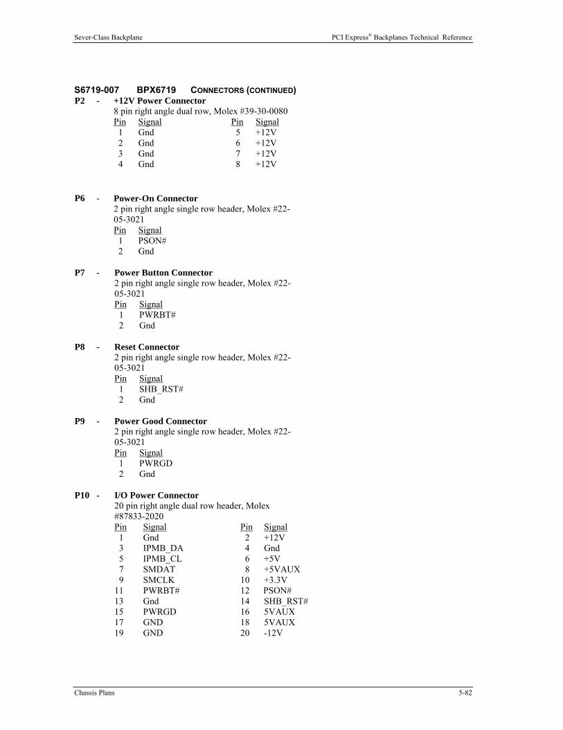
Sever-Class Backplane PCI Express® Backplanes Technical Reference
Chassis Plans 5-82
S6719-007 BPX6719 CONNECTORS (CONTINUED) P2 - +12V Power Connector
8 pin right angle dual row, Molex #39-30-0080
Pin
1
2
3
4
Signal
Gnd
Gnd
Gnd
Gnd
Pin
5
6
7
8
Signal
+12V
+12V
+12V
+12V
P6 - Power-On Connector 2 pin right angle single row header, Molex #22-
05-3021
Pin
1
2
Signal
PSON#
Gnd
P7 - Power Button Connector 2 pin right angle single row header, Molex #22-
05-3021
Pin
1
2
Signal
PWRBT#
Gnd
P8 - Reset Connector 2 pin right angle single row header, Molex #22-
05-3021
Pin
1
2
Signal
SHB_RST#
Gnd
P9 - Power Good Connector 2 pin right angle single row header, Molex #22-
05-3021
Pin
1
2
Signal
PWRGD
Gnd
P10 -
I/O Power Connector 20 pin right angle dual row header, Molex
#87833-2020
Pin
1
3
5
7
9
11
13
15
17
19
Signal
Gnd
IPMB_DA
IPMB_CL
SMDAT
SMCLK
PWRBT#
Gnd
PWRGD
GND
GND
Pin
2
4
6
8
10
12
14
16
18
20
Signal
+12V
Gnd
+5V
+5VAUX
+3.3V
PSON#
SHB_RST#
5VAUX
5VAUX
-12V

PCI Express® Backplanes Technical Reference Server-Class Backplane
5-83 Chassis Plans
S6719-007 BPX6719 CONNECTORS (CONTINUED) P11 - Universal Serial Bus (USB) Connector
8 pin dual row header, Molex #702-46-0801
(+5V fused with self-resetting fuses)
Pin
1
3
5
7
Signal
+5V-USB0
USB0-
USB0+
Gnd-USB0
Pin
2
4
6
8
P12 -
Signal
+5V-USB1
USB1-
USB1+
Gnd-USB1
Universal Serial Bus (USB) Connector 8 pin dual row header, Molex #702-46-0801
(+5V fused with self-resetting fuses)
Pin
1
3
5
7
Signal
+5V-USB2
USB2-
USB2+
Gnd-USB2
Pin
2
4
6
8
P13 -
Signal
+5V-USB3
USB3-
USB3+
Gnd-USB3
10/100/1000Base-T Ethernet Connector - LAN 0 8 pin right angle shielded RJ-45 connector, Molex #43202-
8919
Pin
1
2
3
4
5
6
7
8
Signal
TRP1+
TRP1-
TRP2+
TRP3+
TRP3-
TRP2-
TRP4+
TRP4-
P19 - SMBUS Connector 2 pin right angle single row header, Molex #22-
05-3021
Pin
1
2
Signal
SMBUS
Gnd

Sever-Class Backplane PCI Express® Backplanes Technical Reference
Chassis Plans 5-84
S6806-000 BPX6806 The BPX6806 is 20-slot form factor, server-class backplane that provides eighteen (18) PCI Express option
card slots. Each card slot has a x16 PCIe mechanical connector and the slots use a variety of x8 and x4 PCI
Express links from a server-class System host Board and a Chassis Plans IOB31.
The server-class SHB supplies the x8 PCIe links to the two PCI Express fan-out switch devices that in turn
provide the interface between sixteen (16) of the option card slots and the SHB. The remaining two card
slots are driven directly by the SHB and by the SHB via a Chassis Plans IOB31 module.
All of the card slots on the BPX6806 are PCI Express, x16 mechanical slots and can support x16, x8, x4
and x1 PCI Express cards. The actual speed of a specific PCI Express connection from the SHB to an
option card slot is determined by the SHB’s PCI Express link configuration and the auto-negotiation/link
training features of PCI Express.
The BPX6806 supports the optional Ethernet routing feature of the SHB Express specification. Two
10/100/1000Base-T Ethernet RJ-45 connectors are available for use on the backplane. It also has two USB
2.0 headers which are capable of supporting up to four USB 2.0 ports on the backplane.
USB and Ethernet functionality on the BPX6806 is dependent on the SHB providing I/O capability to edge
connector C of the backplane. In order to take advantage of these I/O features, the SHB in the system must
be able to support the connections as specified in the PCI Industrial Computer Manufacturers Group’s SHB Express™ System Host Board PCI Express Specification, PICMG® 1.3.
The standard BPX6806 backplane is available with a vertical ATX/EPS power connector and two auxiliary
12VDC vertical power connectors suitable for use with either an ATX or EPS power supply. Additional
high-current terminal blocks and right-angle power connectors are also available.
Each PCI Express option card slot on the backplane supports a maximum 75W of power as defined in
revision 1.1 of the PCI Express Base Specification. The Chassis Plans SHB and a x16 option card plugged
into a backplane slot will auto-negotiate to ensure data communication between the SHB and the card, but
care must taken to ensure that adequate card slot power is available when using a backplane slot to support
a x16 card.
The following table illustrates the maximum current delivery possible with each available BPX6806 power
connector configuration.
Connector Configuration 3.3V Total
Current
Delivery (A)
5V Total
Current
Delivery (A)
GND Total
Current
Delivery (A)
12V Total
Current
Delivery (A)
-001 (P1, P2, P22) 24 30 96 60
-002 (P48, P49) 120 0 150 30
-003 (P1, P2, P22, P48, P49) 144 30 246 90
-004 (P1, P2, P22, P3, P4, P5) 136 50 396 200
______________________________________________________________________
CAUTION: In some ATX/EPS systems, the power may appear to be off while the +5VSB signal is still
present and supplying power to the SHB, option cards and other system components. The +5VAUX LED
on a Chassis Plans PICMG 1.3 backplane monitors the +5VSB power signal; “green” indicates that the
+5VSB signal is present. Chassis Plans backplane LEDs monitor all DC power signals, and all of the
LEDs should be off before adding or removing components. Removing boards under power may result in
system damage.
______________________________________________________________________
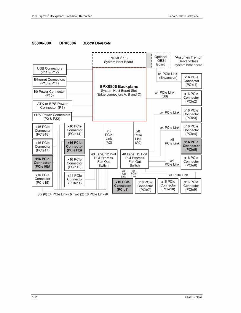
PCI Express® Backplanes Technical Reference Server-Class Backplane
5-85 Chassis Plans
S6806-000 BPX6806 BLOCK DIAGRAM

Sever-Class Backplane PCI Express® Backplanes Technical Reference
Chassis Plans 5-86
S6806-000 BPX6806 DIMENSIONAL DRAWING

PCI Express® Backplanes Technical Reference Server-Class Backplane
5-87 Chassis Plans
CONFIGURATION JUMPER The setup of the configuration jumper on the backplane is described below. * indicates the default value of
the jumper.
NOTE: For the two-position jumper (3-post), “RIGHT” and “LEFT” refer to positioning when the
backplane is viewed with the slots at the top end of the backplane.
Jumper
JU4
Description
+5V Auxiliary Vo ltage Install on the LEFT if +5V auxiliary voltage is provided by the
standard +5V supply. This option is used for systems which do
not have either an ATX or EPS standard power input. This
mode provides the necessary +5V for the SHB’s +5VAUX
signal lines. Sleep mode recovery is not supported using non-
ATX/EPS power supplies.
Install on the RIGHT if +5V auxiliary voltage is provided by a
separate +5VAUX signal input pin. This enables the necessary
SHB power signaling and allows recovery from sleep mode.
This option is used for ATX or EPS standard power supplies. *
S6806-001 BPX6806 CONNECTORS
NOTE: Pin 1 on the connectors is indicated by the square pad on the PCB.
P1 - ATX/EPS Power Connector 24 pin vertical dual row, Molex #44206-002
Pin
1
2
3
4
5
6
7
8
9
10
11
12
Signal
+3.3V
+3.3V
Gnd
+5V
Gnd
+5V
Gnd
PWRGD
+5VAUX
+12V
+12V
+3.3V
Pin
13
14
15
16
17
18
19
20
21
22
23
24
Signal
+3.3V
-12V
Gnd
PSON#
Gnd
Gnd
Gnd
-5V
+5V
+5V
+5V
Gnd

Sever-Class Backplane PCI Express® Backplanes Technical Reference
Chassis Plans 5-88
S6806-001 BPX6806 CONNECTORS (CONTINUED)
P2 - +12V Power Connector 8 pin vertical dual row, Molex #44206-0005
Pin
1
2
3
4
Signal
Gnd
Gnd
Gnd
Gnd
Pin
8
7
6
5
Signal
+12V
+12V
+12V
+12V
P6 - Power-On Connector 2 pin vertical single row header, Amp #640456-2
Pin
1
2
Signal
PSON#
Gnd
P7 - Power Button Connector 2 pin vertical single row header, Amp #640456-2
Pin
1
2
Signal
PWRBT#
Gnd
P8 - Reset Connector 2 pin vertical single row header, Amp #640456-2
Pin
1
2
Signal
SHB_RST#
Gnd
P9 - Power Good Connector 2 pin vertical single row header, Amp #640456-2
Pin
1
2
Signal
PWRGD
+5V
P10 - I/O Power Connector 20 pin vertical dual row header, Molex #87831-2020
Pin
1
3
5
7
9
11
13
15
17
19
Signal
Gnd
IPMB_DA
IPMB_CL
SMDAT
SMCLK
PWRBT#
Gnd
PWRGD
Gnd
Gnd
Pin
2
4
6
8
10
12
14
16
18
20
Signal
+12V
Gnd
+5V
+5VAUX
+3.3V
PSON#
SHB_RST#
5VAUX
5VAUX
-12V

PCI Express® Backplanes Technical Reference Server-Class Backplane
5-89 Chassis Plans
S6806-001 BPX6806 CONNECTORS (CONTINUED)
P11 - Universal Serial Bus (USB) Connector 8 pin dual row header, Molex #702-46-0801
(+5V fused with self-resetting fuses)
Pin
1
3
5
7
Signal
+5V-USB0
USB0-
USB0+
Gnd-USB0
Pin
2
4
6
8
Signal
+5V-USB1
USB1-
USB1+
Gnd-USB1
P12 - Universal Serial Bus (USB) Connector 8 pin dual row header, Molex #702-46-0801
(+5V fused with self-resetting fuses)
Pin
1
3
5
7
Signal
+5V-USB2
USB2-
USB2+
Gnd-USB2
Pin
2
4
6
8
Signal
+5V-USB3
USB3-
USB3+
Gnd-USB3
P13 - 10/100/1000Base-T Ethernet Connector - LAN 0 8 pin right angle shielded RJ-45 connector, Molex #43860-0025
Pin
1
2
3
4
5
6
7
8
Signal
TRP1+
TRP1-
TRP2+
TRP3+
TRP3-
TRP2-
TRP4+
TRP4-
P14 - 10/100/1000Base-T Ethernet Connector - LAN 1 8 pin right angle shielded RJ-45 connector, Molex #43860-0025
Pin
1
2
3
4
5
6
7
8
Signal
TRP1+
TRP1-
TRP2+
TRP3+
TRP3-
TRP2-
TRP4+
TRP4-
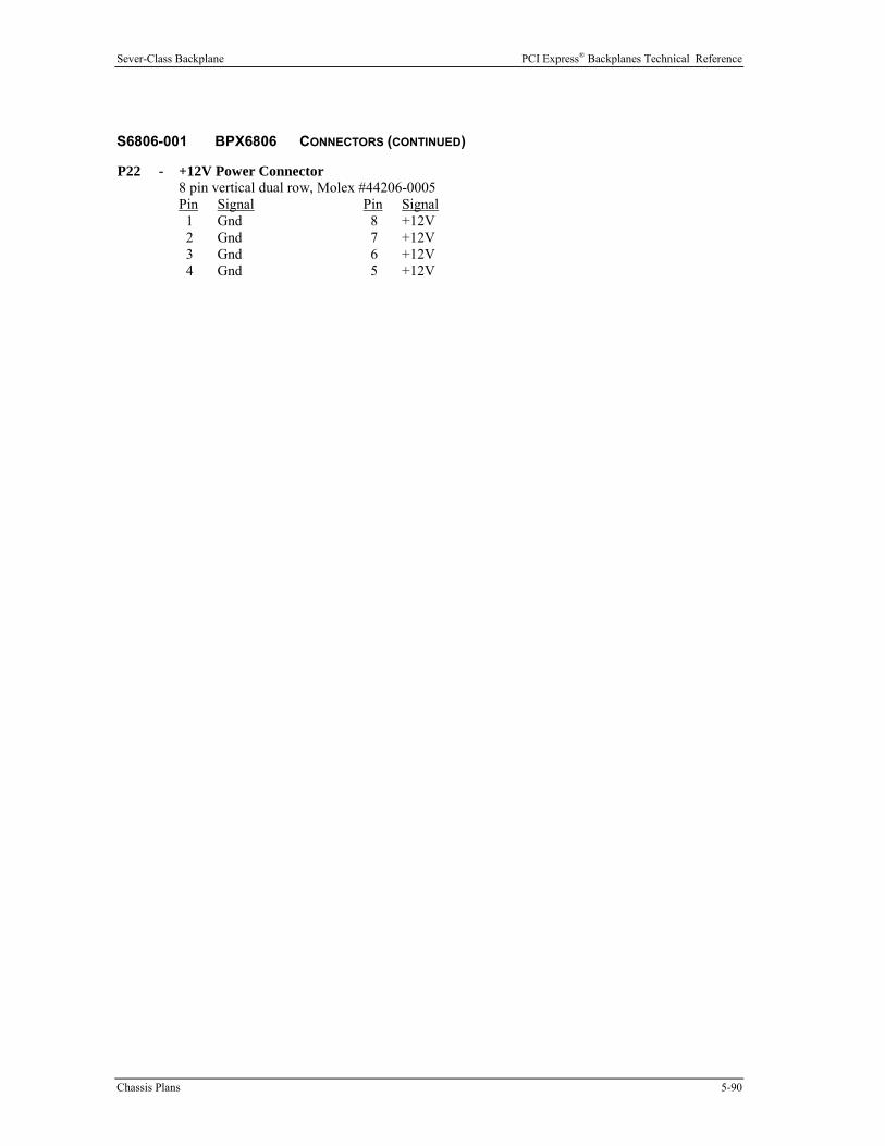
Sever-Class Backplane PCI Express® Backplanes Technical Reference
Chassis Plans 5-90
S6806-001 BPX6806 CONNECTORS (CONTINUED)
P22 - +12V Power Connector 8 pin vertical dual row, Molex #44206-0005
Pin
1
2
3
4
Signal
Gnd
Gnd
Gnd
Gnd
Pin
8
7
6
5
Signal
+12V
+12V
+12V
+12V

PCI Express® Backplanes Technical Reference Server-Class Backplane
5-91 Chassis Plans
S6806-002 BPX6806 CONNECTORS (CONTINUED)
NOTE: Pin 1 on the connectors is indicated by the square pad on the PCB.
P6 - Power-On Connector 2 pin vertical single row header, Amp #640456-2
Pin
1
2
Signal
PSON#
Gnd
P7 - Power Button Connector 2 pin vertical single row header, Amp #640456-2
Pin
1
2
Signal
PWRBT#
Gnd
P8 - Reset Connector 2 pin vertical single row header, Amp #640456-2
Pin
1
2
Signal
SHB_RST#
Gnd
P9 - Power Good Connector 2 pin vertical single row header, Amp #640456-2
Pin
1
2
Signal
PWRGD
+5V
P10 - I/O Power Connector 20 pin vertical dual row header, Molex #87831-2020
Pin
1
3
5
7
9
11
13
15
17
19
Signal
Gnd
IPMB_DA
IPMB_CL
SMDAT
SMCLK
PWRBT#
Gnd
PWRGD
Gnd
Gnd
Pin
2
4
6
8
10
12
14
16
18
20
Signal
+12V
Gnd
+5V
+5VAUX
+3.3V
PSON#
SHB_RST#
5VAUX
5VAUX
-12V

Sever-Class Backplane PCI Express® Backplanes Technical Reference
Chassis Plans 5-92
S6806-002 BPX6806 CONNECTORS (CONTINUED)
P11 - Universal Serial Bus (USB) Connector 8 pin dual row header, Molex #702-46-0801
(+5V fused with self-resetting fuses)
Pin
1
3
5
7
Signal
+5V-USB0
USB0-
USB0+
Gnd-USB0
Pin
2
4
6
8
Signal
+5V-USB1
USB1-
USB1+
Gnd-USB1
P12 - Universal Serial Bus (USB) Connector 8 pin dual row header, Molex #702-46-0801
(+5V fused with self-resetting fuses)
Pin
1
3
5
7
Signal
+5V-USB2
USB2-
USB2+
Gnd-USB2
Pin
2
4
6
8
Signal
+5V-USB3
USB3-
USB3+
Gnd-USB3
P13 - 10/100/1000Base-T Ethernet Connector - LAN 0 8 pin right angle shielded RJ-45 connector, Molex #43860-0025
Pin
1
2
3
4
5
6
7
8
Signal
TRP1+
TRP1-
TRP2+
TRP3+
TRP3-
TRP2-
TRP4+
TRP4-
P14 - 10/100/1000Base-T Ethernet Connector - LAN 1 8 pin right angle shielded RJ-45 connector, Molex #43860-0025
Pin
1
2
3
4
5
6
7
8
Signal
TRP1+
TRP1-
TRP2+
TRP3+
TRP3-
TRP2-
TRP4+
TRP4-

PCI Express® Backplanes Technical Reference Server-Class Backplane
5-93 Chassis Plans
S6806-002 BPX6806 CONNECTORS (CONTINUED)
P48 - DC Return Extended-Current Connector 5 pin right angle, Amp# 193839-4
Pin
1
2
3
4
5
Signal
Gnd
Gnd
Gnd
Gnd
Gnd
P49 - DC Extended-Current Connector 5 pin right angle, Amp# 193839-4
Pin
1
2
3
4
5
Signal
+3.3V
+3.3V
+3.3V
+3.3V
+12V

Sever-Class Backplane PCI Express® Backplanes Technical Reference
Chassis Plans 5-94
S6806-003 BPX6806 CONNECTORS (CONTINUED)
NOTE: Pin 1 on the connectors is indicated by the square pad on the PCB.
P1 - ATX/EPS Power Connector 24 pin vertical dual row, Molex #44206-002
Pin
1
2
3
4
5
6
7
8
9
10
11
12
Signal
+3.3V
+3.3V
Gnd
+5V
Gnd
+5V
Gnd
PWRGD
+5VAUX
+12V
+12V
+3.3V
Pin
13
14
15
16
17
18
19
20
21
22
23
24
Signal
+3.3V
-12V
Gnd
PSON#
Gnd
Gnd
Gnd
-5V
+5V
+5V
+5V
Gnd
P2 - +12V Power Connector 8 pin vertical dual row, Molex #44206-0005
Pin
1
2
3
4
Signal
Gnd
Gnd
Gnd
Gnd
Pin
8
7
6
5
Signal
+12V
+12V
+12V
+12V
P6 - Power-On Connector 2 pin vertical single row header, Amp #640456-2
Pin
1
2
Signal
PSON#
Gnd
P7 - Power Button Connector 2 pin vertical single row header, Amp #640456-2
Pin
1
2
Signal
PWRBT#
Gnd
P8 - Reset Connector 2 pin vertical single row header, Amp #640456-2
Pin
1
2
Signal
SHB_RST#
Gnd

PCI Express® Backplanes Technical Reference Server-Class Backplane
5-95 Chassis Plans
S6806-003 BPX6806 CONNECTORS (CONTINUED)
P9 - Power Good Connector 2 pin vertical single row header, Amp #640456-2
Pin
1
2
Signal
PWRGD
+5V
P10 - I/O Power Connector 20 pin vertical dual row header, Molex #87831-2020
Pin
1
3
5
7
9
11
13
15
17
19
Signal
Gnd
IPMB_DA
IPMB_CL
SMDAT
SMCLK
PWRBT#
Gnd
PWRGD
Gnd
Gnd
Pin
2
4
6
8
10
12
14
16
18
20
Signal
+12V
Gnd
+5V
+5VAUX
+3.3V
PSON#
SHB_RST#
5VAUX
5VAUX
-12V
P11 - Universal Serial Bus (USB) Connector 8 pin dual row header, Molex #702-46-0801
(+5V fused with self-resetting fuses)
Pin
1
3
5
7
Signal
+5V-USB0
USB0-
USB0+
Gnd-USB0
Pin
2
4
6
8
Signal
+5V-USB1
USB1-
USB1+
Gnd-USB1
P12 - Universal Serial Bus (USB) Connector 8 pin dual row header, Molex #702-46-0801
(+5V fused with self-resetting fuses)
Pin
1
3
5
7
Signal
+5V-USB2
USB2-
USB2+
Gnd-USB2
Pin
2
4
6
8
Signal
+5V-USB3
USB3-
USB3+
Gnd-USB3

Sever-Class Backplane PCI Express® Backplanes Technical Reference
Chassis Plans 5-96
S6806-003 BPX6806 CONNECTORS (CONTINUED)
P13 - 10/100/1000Base-T Ethernet Connector - LAN 0 8 pin right angle shielded RJ-45 connector, Molex #43860-0025
Pin
1
2
3
4
5
6
7
8
Signal
TRP1+
TRP1-
TRP2+
TRP3+
TRP3-
TRP2-
TRP4+
TRP4-
P14 - 10/100/1000Base-T Ethernet Connector - LAN 1 8 pin right angle shielded RJ-45 connector, Molex #43860-0025
Pin
1
2
3
4
5
6
7
8
Signal
TRP1+
TRP1-
TRP2+
TRP3+
TRP3-
TRP2-
TRP4+
TRP4-
P22 - +12V Power Connector 8 pin vertical dual row, Molex #44206-0005
Pin
1
2
3
4
Signal
Gnd
Gnd
Gnd
Gnd
Pin
8
7
6
5
Signal
+12V
+12V
+12V
+12V
P48 - DC Return Extended-Current Connector 5 pin right angle, Amp# 193839-4
Pin
1
2
3
4
5
Signal
Gnd
Gnd
Gnd
Gnd
Gnd
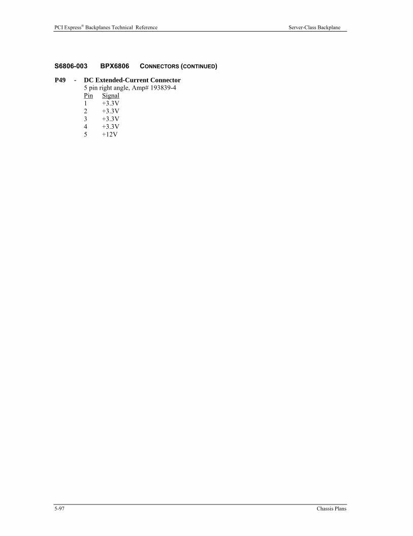
PCI Express® Backplanes Technical Reference Server-Class Backplane
5-97 Chassis Plans
S6806-003 BPX6806 CONNECTORS (CONTINUED)
P49 - DC Extended-Current Connector 5 pin right angle, Amp# 193839-4
Pin
1
2
3
4
5
Signal
+3.3V
+3.3V
+3.3V
+3.3V
+12V

Sever-Class Backplane PCI Express® Backplanes Technical Reference
Chassis Plans 5-98
S6806-004 BPX6806 CONNECTORS (CONTINUED)
NOTE: Pin 1 on the connectors is indicated by the square pad on the PCB.
P1 - ATX/EPS Power Connector 24 pin vertical dual row, Molex #44206-002
Pin
1
2
3
4
5
6
7
8
9
10
11
12
Signal
+3.3V
+3.3V
Gnd
+5V
Gnd
+5V
Gnd
PWRGD
+5VAUX
+12V
+12V
+3.3V
Pin
13
14
15
16
17
18
19
20
21
22
23
24
Signal
+3.3V
-12V
Gnd
PSON#
Gnd
Gnd
Gnd
-5V
+5V
+5V
+5V
Gnd
P2 - +12V Power Connector 8 pin vertical dual row, Molex #44206-0005
Pin
1
2
3
4
Signal
Gnd
Gnd
Gnd
Gnd
Pin
8
7
6
5
Signal
+12V
+12V
+12V
+12V
P3 - Terminal Block Connector 10 position terminal block, Amp #1-796949-0
20 Amps per circuit
Pin
1
2
3
4
5
6
7
8
9
10
Signal
+3.3V
+3.3V
+3.3V
+3.3V
+3.3V
Gnd
Gnd
Gnd
Gnd
Gnd

PCI Express® Backplanes Technical Reference Server-Class Backplane
5-99 Chassis Plans
S6806-004 BPX6806 CONNECTORS (CONTINUED) P4 - Terminal Block Connector
10 position terminal block, Amp #1-796949-0
20 Amps per circuit
Pin
1
2
3
4
5
6
7
8
9
10
Signal
+12V
+12V
+5V
+3.3V
+3.3V
Gnd
Gnd
Gnd
Gnd
Gnd
P5 - Terminal Block Connector 10 position terminal block, Amp #1-796949-0
20 Amps per circuit
Pin
1
2
3
4
5
6
7
8
9
10
Signal
+12V
+12V
+12V
+12V
+12V
Gnd
Gnd
Gnd
Gnd
Gnd
P6 - Power-On Connector 2 pin vertical single row header, Amp #640456-2
Pin
1
2
Signal
PSON#
Gnd
P7 - Power Button Connector 2 pin vertical single row header, Amp #640456-2
Pin
1
2
Signal
PWRBT#
Gnd
P8 - Reset Connector 2 pin vertical single row header, Amp #640456-2
Pin
1
2
Signal
SHB_RST#
Gnd

Sever-Class Backplane PCI Express® Backplanes Technical Reference
Chassis Plans 5-100
S6806-004 BPX6806 CONNECTORS (CONTINUED)
P9 - Power Good Connector 2 pin vertical single row header, Amp #640456-2
Pin
1
2
Signal
PWRGD
+5V
P10 - I/O Power Connector 20 pin vertical dual row header, Molex #87831-2020
Pin
1
3
5
7
9
11
13
15
17
19
Signal
Gnd
IPMB_DA
IPMB_CL
SMDAT
SMCLK
PWRBT#
Gnd
PWRGD
Gnd
Gnd
Pin
2
4
6
8
10
12
14
16
18
20
Signal
+12V
Gnd
+5V
+5VAUX
+3.3V
PSON#
SHB_RST#
5VAUX
5VAUX
-12V
P11 - Universal Serial Bus (USB) Connector 8 pin dual row header, Molex #702-46-0801
(+5V fused with self-resetting fuses)
Pin
1
3
5
7
Signal
+5V-USB0
USB0-
USB0+
Gnd-USB0
Pin
2
4
6
8
Signal
+5V-USB1
USB1-
USB1+
Gnd-USB1
P12 - Universal Serial Bus (USB) Connector 8 pin dual row header, Molex #702-46-0801
(+5V fused with self-resetting fuses)
Pin
1
3
5
7
Signal
+5V-USB2
USB2-
USB2+
Gnd-USB2
Pin
2
4
6
8
Signal
+5V-USB3
USB3-
USB3+
Gnd-USB3

PCI Express® Backplanes Technical Reference Server-Class Backplane
5-101 Chassis Plans
S6806-004 BPX6806 CONNECTORS (CONTINUED)
P13 - 10/100/1000Base-T Ethernet Connector - LAN 0 8 pin right angle shielded RJ-45 connector, Molex #43860-0025
Pin
1
2
3
4
5
6
7
8
Signal
TRP1+
TRP1-
TRP2+
TRP3+
TRP3-
TRP2-
TRP4+
TRP4-
P14 - 10/100/1000Base-T Ethernet Connector - LAN 1 8 pin right angle shielded RJ-45 connector, Molex #43860-0025
Pin
1
2
3
4
5
6
7
8
Signal
TRP1+
TRP1-
TRP2+
TRP3+
TRP3-
TRP2-
TRP4+
TRP4-
P22 - +12V Power Connector 8 pin vertical dual row, Molex #44206-0005
Pin
1
2
3
4
Signal
Gnd
Gnd
Gnd
Gnd
Pin
8
7
6
5
Signal
+12V
+12V
+12V
+12V


PCI Express® Backplanes Technical Reference Multi-Segment Backplanes
6-1 Chassis Plans
Chapter 6 - Multiple SHB Segment Backplanes
S6605-000 BP6FS6605 The BP6FS6605 is a six-segment, PICMG-compatible backplane which is a six-layer .080" thick PCB.
The six SHB segments are flexible enough to be ordered in either a graphics-class or server-class
configuration. It is PICMG® 1.3 compliant and supports Chassis Plans and PICMG
® 1.3 14-slot (64-bit)
mounting hole patterns.
In a graphics-class configuration of the BP6FS6605, the SHB slot in each backplane segment supports a
graphics-class PICMG 1.3 system host board such as Chassis Plans's TML. Each graphics-class SHB
segment supports the segment's x16 PCI Express (PCIe) mechanical slot with a x16 PCIe electrical link
from the SHB. There is one x16 PCIe mechanical slot for each SHB segment: PCIe1-2, PCIe2-2, PCIe3-2,
PCIe4-1, PCIe5-1 and PCIe6-1.
In a server-class configuration of the BP6FS6605, the SHB slot in each backplane segment supports server-
class PICMG 1.3 system host boards such as the Chassis Plans SLT or SLI. Each server-class SHB
segment supports the x16 PCI Express (PCIe) mechanical slot with a x8 PCIe electrical link from the SHB.
SHB segments A1, A2 and A3 also feature a x8 PCIe mechanical slot. These slots are labeled PCIe1-1,
PCIe2-1 and PCIe3-1 and are driven by an SHB's x4 PCI Express link in both graphics-class and server-
class configurations of the backplane.
Chassis Plans's BP6FS6605 backplane is available with an optional Ethernet fabric to enable the SHBs in
each segment to share data and communicate information to and from the system host via the backplane's
Ethernet hub port. The backplane's optional Ethernet hub switch makes this functionality possible. The
Ethernet hub switch controls the SHB-to-SHB communication and the SHB's communication to the host
system via the 10/100Base-T Ethernet port interface. This optional backplane capability requires that the
SHB support the optional Ethernet interface routing to SHB edge connector C as defined in the PICMG 1.3
or SHB Express specification. The Ethernet fabric on the BP6FS6605 backplane enables many system
advantages in applications that require cluster computing.
Each backplane segment provides soft control power circuitry to control the power-up and power-down
sequences of each SHB segment. Connecting an independent power source to each segment maximizes the
power control aspect of each backplane segment. The BP6FS6605 backplane allows segments to be
powered individually or grouped together for the purpose of being powered by a single power source. Care
must be used when grouping segments together to ensure that adequate power is provided and the desired
power sequences are controlled.
The BP6FS6605 backplane supports two backplane connector option types: ATX/EPS and terminal
blocks.
In the ATX/EPS configuration, each SHB segment is usually powered by a separate ATX or EPS power
supply. A 24-pin vertical power connector in each SHB segment provides the interface to the segment's
power supply. Each segment also includes a +12V auxiliary power connector for routing the auxiliary
power directly to the SHB's edge connectors. This new capability of PICMG 1.3 compliant SHBs and
backplanes eliminates the need for auxiliary power connections on the system host board. The BP6FS6605
backplane power connectors used in the standalone configuration are suitable for use with either an ATX or
EPS power supply.
The terminal block connectors enable each SHB segment or multiple segments to be powered by a +12V
power source. The voltage regulator circuits in each SHB segment provide all of the required voltage
levels for the SHB and option card slots. Using the terminal blocks is the recommended method for
grouping together segments in order to drive multiple segments with a common power supply. (Note:

Multi-Segment Backplanes PCI Express® Backplanes Technical Reference
Chassis Plans 6-2
grouping segments with the standard ATX/EPS power connectors is also allowed, but Chassis Plans
recommends using the terminal blocks for this type of multiple SHB segment power connection.) Each
segment's four-position terminal block provides additional power capacity and up to 80 Amps of +12V.
CAUTION: In some ATX/EPS systems, the power may appear to be off while the +5VSB signal is still
present and supplying power to the SHB, option cards and other system components. The +5VAUX LED
on a Chassis Plans PICMG 1.3 backplane monitors the +5VSB power signal; “green” indicates that the
+5VSB signal is present. Chassis Plans backplane LEDs monitor all DC power signals, and all of the
LEDs should be off before adding or removing components. Removing boards under power may result in
system damage.
Models with other power configurations may be available. Contact Chassis Plans for more information.
S6605-000 BP6FS66055 BLOCK DIAGRAM

PCI Express® Backplanes Technical Reference Multi-Segment Backplanes
6-3 Chassis Plans
S6605-000 BP6FS6605 DIMENSIONAL DRAWING
Chassis Plans Hole Pattern
Note: Connectors and components on the layout drawings shown in dotted lines may or may not be
populated on your specific model of the BP6FS66005 backplane. Refer to Backplane Configuration
Table.

Multi-Segment Backplanes PCI Express® Backplanes Technical Reference
Chassis Plans 6-4
S6605-000 BP6FS6605 DIMENSIONAL DRAWING
PICMG 1.3 Hole Pattern
Note: Connectors and components on the layout drawings shown in dotted lines may or may not be
populated on your specific model of the BP6FS66005 backplane. Refer to Backplane Configuration
Table.

PCI Express® Backplanes Technical Reference Multi-Segment Backplanes
6-5 Chassis Plans
S6605-000 BP6FS6605 BACKPLANE CONFIGURATION TABLE Model# Model Name &
Type SHB Connector D
ATX/EPS Connectors P1-1 P2-1 P3-1 P4-1 P5-1 P6-1
+12V Aux Connectors P1-2 P2-2 P3-2 P4-2 P5-2 P6-2
+12V Terminal Blocks P1-3 P2-3 P3-3 P4-3 P5-3 P6-3
Ethernet Hub
Ethernet Hub Port P13
S6605-005 BP6FS6605-SCSV, Server-class, Standalone, Vertical ATX/EPS connectors
No Yes Yes No No No
S6605-016 BP6FS6605-SCST, Server-class, Standalone, Terminal Block connectors
No No No Yes No No
S6605-025 BP6FS6605-SCEV, Server-class, Ethernet, Vertical ATX/EPS connectors
No Yes Yes No Yes* Yes*
S6605-036 BP6FS6605-SCET, Server-class, Ethernet, Terminal Block connectors
No No No Yes Yes* Yes*
S6605-105 BP6FS6605-GCSV, Graphics-class, Standalone, Vertical ATX/EPS connectors
Yes Yes Yes No No No
S6605-116 BP6FS6605-GCST, Graphics-class, Standalone, Terminal Block connectors
Yes No No Yes No No
S6605-125 BP6FS6605-GCEV,Graphics-class, Ethernet, Vertical ATX/EPS connectors
Yes Yes Yes No Yes Yes
S6605-136 BP6FS6605-GCET, Graphics-class, Ethernet, Terminal Block connectors
Yes No No Yes Yes Yes
*CHASSIS PLANS SLT/SLI SYSTEM HOST BOARDS DO NOT SUPPORT THIS FUNCTION ON THE BACKPLANE

Multi-Segment Backplanes PCI Express® Backplanes Technical Reference
Chassis Plans 6-6
CONFIGURATION JUMPER The setup of the configuration jumper on the backplane is described below. * indicates the default value of
the jumper.
NOTE: For the two-position jumper (3-post) in SHB segments 1 and 2, “RIGHT” and “LEFT” refer to
positioning when the backplane is viewed with the SHB’s I/O plate(s) at the top end of the backplane.
NOTE: For the two-position jumper (3-post) in SHB segments 3, 4, 5 and 6, “TOP” and “BOTTOM” refer
to positioning when the backplane is viewed with the SHB’s I/O plate(s) at the top end of the backplane.
Jumper
JU4, 1-2
Description
+5V Auxil iary Voltage Install on the LEFT if +5V auxiliary voltage is provided by the
standard +5V supply. This option is used for systems which do
not have either an ATX or EPS standard power input. This
mode provides the necessary +5V for the SHB’s +5VAUX
signal lines. Sleep mode recovery is not supported using non-
ATX/EPS power supplies. *
Install on the RIGHT if +5V auxiliary voltage is provided by a
separate +5VAUX signal input pin. This enables the necessary
SHB power signaling and allows recovery from sleep mode.
This option is used for ATX or EPS standard power supplies.
JU4, 3-6 +5V Auxiliary Voltage Install on the TOP if +5V auxiliary voltage is provided by the
standard +5V supply. This option is used for systems which do
not have either an ATX or EPS standard power input. This
mode provides the necessary +5V for the SHB’s +5VAUX
signal lines. Sleep mode recovery is not supported using non-
ATX/EPS power supplies. *
Install on the BOTTOM if +5V auxiliary voltage is provided by
a separate +5VAUX signal input pin. This enables the
necessary SHB power signaling and allows recovery from sleep
mode. This option is used for ATX or EPS standard power
supplies.

PCI Express® Backplanes Technical Reference Multi-Segment Backplanes
6-7 Chassis Plans
S6605-000 BP6FS6605 CONNECTORS
NOTE: Pin 1 on the connectors is indicated by the square pad on the PCB.
P1, 1-6 - EPS Power Connector 24 pin vertical dual row, Molex #44206-0007
Pin
1
2
3
4
5
6
7
8
9
10
11
12
Signal
+3.3V
+3.3V
Gnd
+5V
Gnd
+5V
Gnd
PWRGD
+5VAUX
+12V
+12V
+3.3V
Pin
13
14
15
16
17
18
19
20
21
22
23
24
Signal
+3.3V
-12V
Gnd
PSON#
Gnd
Gnd
Gnd
-5V
+5V
+5V
+5V
Gnd
P2, 1-6 - +12V Power Connector 8 pin vertical dual row, Molex #44206-0005
Pin
1
2
3
4
Signal
Gnd
Gnd
Gnd
Gnd
Pin
5
6
7
8
P3, 1-6 -
Signal
+12V
+12V
+12V
+12V
Terminal Block Connector 4 position terminal block, AMP, #796949-4
20 Amps per circuit
Pin
1
2
3
4
P6 -
Signal
+12V
+12V
Gnd
Gnd
Power-On Connector 14 pin dual row connector, 3M, #N2514-6002RB
Pin
1
3
5
7
9
11
13
Signal
PSON# - 1
PSON# - 2
PSON# - 3
PSON# - 4
PSON# - 5
PSON# - 6
NC
Pin
2
4
6
8
10
12
14
Signal
Gnd - 1
Gnd - 2
Gnd - 3
Gnd - 4
Gnd - 5
Gnd - 6
NC

Multi-Segment Backplanes PCI Express® Backplanes Technical Reference
Chassis Plans 6-8
S6605-000 BP6FS6605 CONNECTORS (CONTINUED) P7 - Power Button Connector
14 pin dual row connector, 3M, #N2514-6002RB
Pin
1
3
5
7
9
11
13
Signal
PWRBT# - 1
PWRBT# - 2
PWRBT# - 3
PWRBT# - 4
PWRBT# - 5
PWRBT# - 6
NC
Pin
2
4
6
8
10
12
14
P8 -
Signal
Gnd - 1
Gnd - 2
Gnd - 3
Gnd - 4
Gnd - 5
Gnd - 6
NC
Reset Connector 14 pin dual row connector, 3M, #N2514-6002RB
Pin
1
3
5
7
9
11
13
Signal
SHB_RST# - 1
SHB_RST# - 2
SHB_RST# - 3
SHB_RST# - 4
SHB_RST# - 5
SHB_RST# - 6
NC
Pin
2
4
6
8
10
12
14
P13 -
Signal
Gnd - 1
Gnd - 2
Gnd - 3
Gnd - 4
Gnd - 5
Gnd - 6
NC
10/100 Base-T Ethernet Connector – Backplane Hub Port 8 pin right angle shielded RJ-45 connector, Pulse, #J0035D21BNL
Pin
1
2
3
4
5
6
7
8
Signal
RXD-
RXD+
RCI
RC
TC
TCI
TXD-
TXD+

PCI Express® Backplanes Technical Reference 2U Butterfly Backplanes
7-1 Chassis Plans
Chapter 7 - 2U Butterfly Backplanes
S6741-000 BPG6741 The BPG6741 is a graphics-class PICMG-compatible backplane which is a six-layer .062" thick PCB. It
supports PICMG®
1.3 compliant SHBs and the butterfly form factor is designed for use in 2U chassis.
The backplane has one PCI Express® slot which accepts an SHB Express™
system host board (SHB). It
also has three Express slots (PCIe1, PCIe3 and PCIe4) which provide the mechanical connections between
the PCI Express option cards and the SHB.
PCIe1 and PCIe3 option card slots are located on side B of the 6741. Side B is opposite the SHB and Side
B slots are driven by x1 PCI Express electrical links from a Chassis Plans MCX-series SHB. PCIe4 is a
x16 mechancial slot located on Side A of the butterfly backplane and is driven by x16 PCI Express
electrical link from a graphics-class SHB. It is capable of supporting high-end PCI Express video and
graphics cards.
The audio controller on the BPG6741 backplane eliminates the need to dedicate an option card slot to a
sound card. The USB audio controller supports a variety of speaker, headset and microphone
configurations. The USB4 port from the Chassis Plans MCG-series SHB provides the input for the USB
audio controller and the USB4 input becomes Audio0 on the BPG6741 backplane.
The BPG6741 supports the optional Ethernet routing feature of the SHB Express specification. The
Ethernet version of the BPG6741 provides one 10/100/1000Base-T Ethernet RJ-45 connector on side B of
the butterfly backplane. The required Ethernet connector location may necessitate a mechanical
modification to the chassis in order to facilitate proper backplane mounting within the enclosure. It also
has one USB 2.0 header which is capable of supporting up to two USB 2.0 general purpose I/O ports on the
backplane.
Audio, USB and Ethernet functionality on the BPG6741 is dependent on the SHB providing the I/O
capability to edge connector C of the backplane. In order to take advantage of these optional I/O features,
the SHB in the system must be able to support the connections as specified in the PCI Industrial
Manufacturers Group’s SHB Express™ System Host Board PCI Express Specification, PICMG® 1.3.
The standard BPG6741 backplane is available with a low-profile right-angle power connector suitable for
use with either an ATX or EPS power supply
CAUTION: In some ATX/EPS systems, the power may appear to be off while the +5VSB signal is still
present and supplying power to the SHB, option cards and other system components. The +5VAUX LED
on a Chassis Plans PICMG 1.3 backplane monitors the +5VSB power signal; “green” indicates that the
+5VSB signal is present. Chassis Plans backplane LEDs monitor all DC power signals, and all of the
LEDs should be off before adding or removing components. Removing boards under power may result in
system damage.
Models with other power configurations may be available. Contact Chassis Plans’ for more information.

2U Butterfly Backplanes PCI Express® Backplanes Technical Reference
Chassis Plans 7-2
S6741-000 BPG6741 BLOCK DIAGRAM

PCI Express® Backplanes Technical Reference 2U Butterfly Backplanes
7-3 Chassis Plans
S6741-000 BPG6741 BLOCK DIAGRAM

2U Butterfly Backplanes PCI Express® Backplanes Technical Reference
Chassis Plans 7-4
CONFIGURATION JUMPER The setup of the configuration jumper on the backplane is described below. * indicates the default value of
the jumper.
NOTE: For the two-position jumper (3-post), “RIGHT” and “LEFT” refer to positioning when the
backplane is viewed with the slots at the top end of the backplane.
Jumper
JU4
Description
+5V Auxiliary Voltage Install on the LEFT if +5V auxiliary voltage is provided by the
standard +5V supply. This option is used for systems which do
not have either an ATX or EPS standard power input. This
mode provides the necessary +5V for the SHB’s +5VAUX
signal lines. Sleep mode recovery is not supported using non-
ATX/EPS power supplies.
Install on the RIGHT if +5V auxiliary voltage is provided by a
separate +5VAUX signal input pin. This enables the necessary
SHB power signaling and allows recovery from sleep mode.
This option is used for ATX or EPS standard power supplies. *
S6741-000 BPG6741 CONNECTORS
NOTE: Pin 1 on the connectors is indicated by the square pad on the PCB.
P1 - ATX/EPS Power Connector 24 pin right angle dual row, Molex #39-30-1240
Pin
1
2
3
4
5
6
7
8
9
10
11
12
Signal
+3.3V
+3.3V
Gnd
+5V
Gnd
+5V
Gnd
PWRGD
+5VAUX
+12V
+12V
+3.3V
Pin
13
14
15
16
17
18
19
20
21
22
23
24
Signal
+3.3V
-12V
Gnd
PSON#
Gnd
Gnd
Gnd
-5V
+5V
+5V
+5V
Gnd

PCI Express® Backplanes Technical Reference 2U Butterfly Backplanes
7-5 Chassis Plans
S6741-000 BPG6741 CONNECTORS (CONTINUED) P2 - +12V Power Connector
8 pin right angle dual row, Molex #39-30-0080
Pin
1
2
3
4
Signal
Gnd
Gnd
Gnd
Gnd
Pin
5
6
7
8
P6 -
Signal
+12V
+12V
+12V
+12V
Power-On Connector 2 pin right angle single row header, Molex #22-
05-3021
Pin
1
2
Signal
PSON#
Gnd
P7 - Power Button Connector 2 pin right angle single row header, Molex #22-
05-3021
Pin
1
2
Signal
PWRBT#
Gnd
P8 - Reset Connector 2 pin right angle single row header, Molex #22-
05-3021
Pin
1
2
Signal
SHB_RST#
Gnd
P9 - Power Good Connector 2 pin right angle single row header, Molex #22-
05-3021
Pin
1
2
Signal
PWRGD
Gnd

2U Butterfly Backplanes PCI Express® Backplanes Technical Reference
Chassis Plans 7-6
S6741-000 BPG6741 CONNECTORS (CONTINUED) P10 -
I/O Power Connector 20 pin right angle dual row header, Molex
#87833-2020
Pin
1
3
5
7
9
11
13
15
17
19
Signal
Gnd
IPMB_DA
IPMB_CL
SMDAT
SMCLK
PWRBT#
Gnd
PWRGD
GND
GND
Pin
2
4
6
8
10
12
14
16
18
20
Signal
+12V
Gnd
+5V
+5VAUX
+3.3V
PSON#
SHB_RST#
5VAUX
5VAUX
-12V
P11 - Universal Serial Bus (USB) Connector 10 pin right angle dual row header, 3M, #N2510-5002UB
(+5V fused with self-resetting fuses)
Pin
1
3
5
7
9
Signal
+5V-USB0
USB0-
USB0+
Gnd-USB0
Chassis Gnd
Pin
2
4
6
8
10
P13 -
Signal
+5V-USB1
USB1-
USB1+
Gnd-USB1
Chassis Gnd
10/100/1000Base-T Ethernet Connector - LAN 0 (Optional) 8 pin right angle shielded RJ-45 connector, Molex #43860-
0025
Pin
1
2
3
4
5
6
7
8
Signal
TRP1+
TRP1-
TRP2+
TRP3+
TRP3-
TRP2-
TRP4+
TRP4-
P19 - SMBUS Connector 2 pin right angle single row header, Molex #22-
05-3021
Pin
1
2
S6741-000 BPG6741 CONNECTORS (CONTINUED)
Signal
SMBUS
Gnd
P30 - Universal Serial Bus (USB) Audio Connector 10 pin right angle dual row header, 3M, #N2510-5002UB
Pin
1
3
5
7
9
Signal
LineIn Lt.
Gnd
Mic P
Gnd
Linout Lt.
Pin
2
4
6
8
10
Signal
LineIn Rt.
Gnd
Mic In
Gnd
LineOut Rt.

PCI Express® Backplanes Technical Reference 2U Butterfly Backplanes
7-7 Chassis Plans