backplane reference manual n - chassis plans manual. models model # model name description pci...
TRANSCRIPT
BACKPLANES
PCI/ISAPCI-X
Revision N
TECHNICAL REFERENCE
The Original Industrial Computer Source®
WARRANTY The product is warranted against material and manufacturing defects for two years from date of delivery. Buyer agrees that if this product proves defective Chassis Plans is only obligated to repair, replace or refund the purchase price of this product at Chassis Plans’ discretion. The warranty is void if the product has been subjected to alteration, neglect, misuse or abuse; if any repairs have been attempted by anyone other than Chassis Plans; or if failure is caused by accident, acts of God, or other causes beyond the control of Chassis Plans. Chassis Plans reserves the right to make changes or improvements in any product without incurring any obligation to similarly alter products previously purchased.
In no event shall Chassis Plans be liable for any defect in hardware or software or loss or inadequacy of data of any kind, or for any direct, indirect, incidental or consequential damages arising out of or in connection with the performance or use of the product or information provided. Chassis Plans’ liability shall in no event exceed the purchase price of the product purchased hereunder. The foregoing limitation of liability shall be equally applicable to any service provided by Chassis Plans.
RETURN POLICY Products returned for repair must be accompanied by a Return Material Authorization (RMA) number, obtained from Chassis Plans prior to return. Freight on all returned items must be prepaid by the customer, and the customer is responsible for any loss or damage caused by common carrier in transit. Items will be returned from Chassis Plans via Ground, unless prior arrangements are made by the customer for an alternative shipping method
To obtain an RMA number, call us at (858) 571-4330. We will need the following infor-mation:
Return company address and contactModel name and model # from the label on the back of the boardSerial number from the label on the back of the boardDescription of the failure
An RMA number will be issued. Mark the RMA number clearly on the outside of each box, include a failure report for each board and return the product(s) to our San Diego, CA facility:
Chassis Plans8295 Aero PlaceSan Diego, CA 92123Attn: Repair Department
TRADEMARKS IBM, PC/AT, VGA, EGA, OS/2 and PS/2 are trademarks or registered trademarksof International Business Machines Corp.
Intel is a registered trademark of Intel Corporation.MS-DOS and Microsoft are registered trademarks of Microsoft Corp.PICMG, SHB Express and the PICMG logo are registered trademarks of the
PCI Industrial Computer Manufacturers Group.All other brand and product names may be trademarks or registered trademarks
of their respective companies.
LIABILITY DISCLAIMER
This manual is as complete and factual as possible at the time of printing; however, the information in this manual may have been updated since that time. Chassis Plans reserves the right to change the functions, features or specifications of their products at any time, without notice.
Copyright © 2007 by Chassis Plans. All rights reserved.
E-mail: [email protected]: www.chassisplans.com
The Original Industrial Computer Source®
Chassis Plans8295 Aero Place • San Diego, CA 92123Sales: (858) 571-4330 • Fax: (858) 571-6146 • Web: www.chassisplans.com
Backplanes Technical Reference
Chassis Plans i
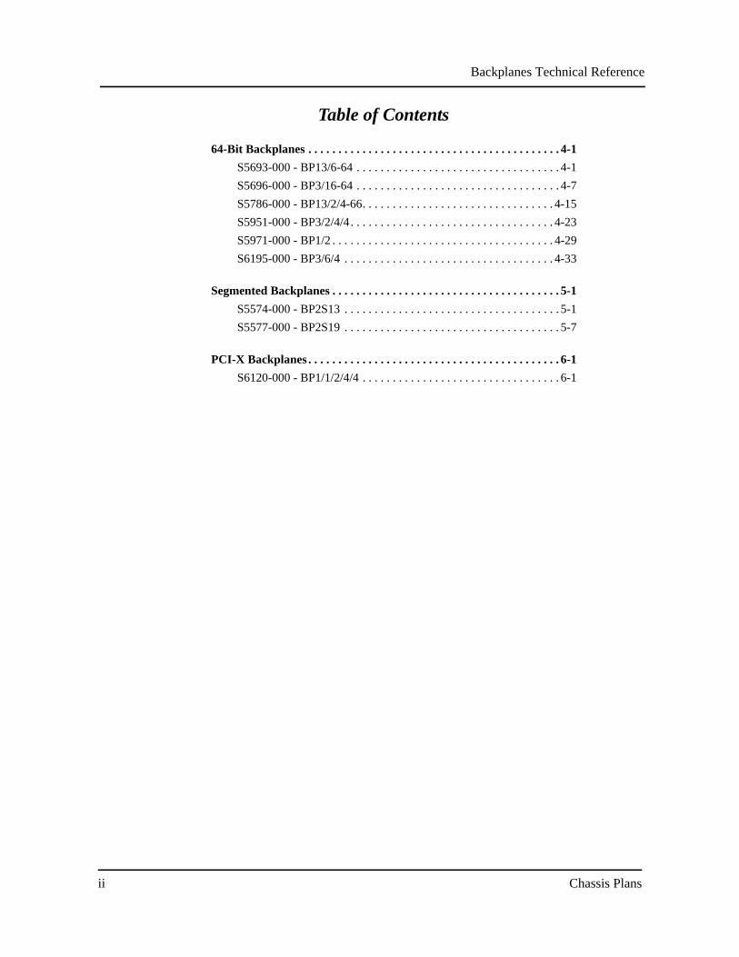
Table of Contents
Backplane Overview . . . . . . . . . . . . . . . . . . . . . . . . . . . . . . . . . . . . . . . . 1-1Introduction . . . . . . . . . . . . . . . . . . . . . . . . . . . . . . . . . . . . . . . . . . . 1-1Models . . . . . . . . . . . . . . . . . . . . . . . . . . . . . . . . . . . . . . . . . . . . . . . 1-1Features . . . . . . . . . . . . . . . . . . . . . . . . . . . . . . . . . . . . . . . . . . . . . . 1-2Backplane Overview . . . . . . . . . . . . . . . . . . . . . . . . . . . . . . . . . . . . 1-2
Bus Architecture. . . . . . . . . . . . . . . . . . . . . . . . . . . . . . . . . . . . 1-2Bus Terminations - ISA Bus. . . . . . . . . . . . . . . . . . . . . . . . . . . 1-2Resistor Termination . . . . . . . . . . . . . . . . . . . . . . . . . . . . . . . . 1-2Keyboard Connectors . . . . . . . . . . . . . . . . . . . . . . . . . . . . . . . . 1-4Power Supply Connectors . . . . . . . . . . . . . . . . . . . . . . . . . . . . 1-4
Terminator Resistor Assignments . . . . . . . . . . . . . . . . . . . . . . . . . . 1-5
ISA/PCI Reference . . . . . . . . . . . . . . . . . . . . . . . . . . . . . . . . . . . . . . . . . 2-1ISA Bus Pin Numbering. . . . . . . . . . . . . . . . . . . . . . . . . . . . . . . . . . 2-1ISA Bus Pin Assignments . . . . . . . . . . . . . . . . . . . . . . . . . . . . . . . . 2-2ISA Bus Signal Descriptions . . . . . . . . . . . . . . . . . . . . . . . . . . . . . . 2-3I/O Address Map . . . . . . . . . . . . . . . . . . . . . . . . . . . . . . . . . . . . . . . 2-7Interrupt Assignments . . . . . . . . . . . . . . . . . . . . . . . . . . . . . . . . . . . 2-7PCI Local Bus Overview . . . . . . . . . . . . . . . . . . . . . . . . . . . . . . . . . 2-8PCI Local Bus Signal Definition . . . . . . . . . . . . . . . . . . . . . . . . . . . 2-9PCI Local Bus Pin Numbering. . . . . . . . . . . . . . . . . . . . . . . . . . . . 2-10PCI Local Bus Pin Assignments . . . . . . . . . . . . . . . . . . . . . . . . . . 2-11PCI Local Bus Signal Descriptions . . . . . . . . . . . . . . . . . . . . . . . . 2-14
PCI/ISA Backplanes . . . . . . . . . . . . . . . . . . . . . . . . . . . . . . . . . . . . . . . . 3-1S5457-000 - BP3/16 . . . . . . . . . . . . . . . . . . . . . . . . . . . . . . . . . . . . . 3-1S5491-000 - BP7/6 . . . . . . . . . . . . . . . . . . . . . . . . . . . . . . . . . . . . . . 3-7S5495-000 - BP13/6 . . . . . . . . . . . . . . . . . . . . . . . . . . . . . . . . . . . . 3-13S5498-000 - BP17/3 . . . . . . . . . . . . . . . . . . . . . . . . . . . . . . . . . . . . 3-19S5501-000 - BP11/3 . . . . . . . . . . . . . . . . . . . . . . . . . . . . . . . . . . . . 3-25S5504-000 - BP5/3 . . . . . . . . . . . . . . . . . . . . . . . . . . . . . . . . . . . . . 3-31S5635-000 - BP8/12 . . . . . . . . . . . . . . . . . . . . . . . . . . . . . . . . . . . . 3-37S5937-000 - BP3/10 . . . . . . . . . . . . . . . . . . . . . . . . . . . . . . . . . . . . 3-43
Backplanes Technical Reference
Chassis Plansii
Table of Contents
64-Bit Backplanes . . . . . . . . . . . . . . . . . . . . . . . . . . . . . . . . . . . . . . . . . . 4-1S5693-000 - BP13/6-64 . . . . . . . . . . . . . . . . . . . . . . . . . . . . . . . . . . 4-1S5696-000 - BP3/16-64 . . . . . . . . . . . . . . . . . . . . . . . . . . . . . . . . . . 4-7S5786-000 - BP13/2/4-66. . . . . . . . . . . . . . . . . . . . . . . . . . . . . . . . 4-15S5951-000 - BP3/2/4/4. . . . . . . . . . . . . . . . . . . . . . . . . . . . . . . . . . 4-23S5971-000 - BP1/2 . . . . . . . . . . . . . . . . . . . . . . . . . . . . . . . . . . . . . 4-29S6195-000 - BP3/6/4 . . . . . . . . . . . . . . . . . . . . . . . . . . . . . . . . . . . 4-33
Segmented Backplanes . . . . . . . . . . . . . . . . . . . . . . . . . . . . . . . . . . . . . . 5-1S5574-000 - BP2S13 . . . . . . . . . . . . . . . . . . . . . . . . . . . . . . . . . . . . 5-1S5577-000 - BP2S19 . . . . . . . . . . . . . . . . . . . . . . . . . . . . . . . . . . . . 5-7
PCI-X Backplanes . . . . . . . . . . . . . . . . . . . . . . . . . . . . . . . . . . . . . . . . . . 6-1S6120-000 - BP1/1/2/4/4 . . . . . . . . . . . . . . . . . . . . . . . . . . . . . . . . . 6-1
Copyright 2006 by Trenton Technology Inc. All rights reserved.
Backplanes Technical Reference
Chassis Plans iii
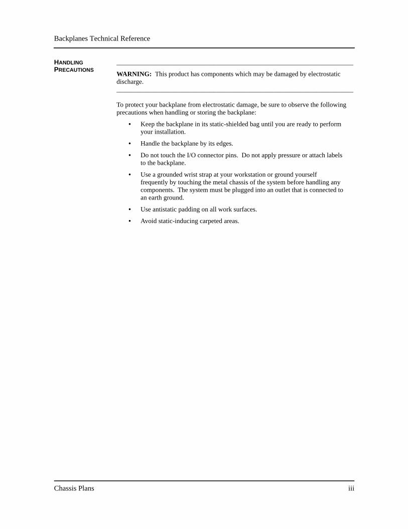
HANDLING PRECAUTIONS
_______________________________________________________________________
WARNING: This product has components which may be damaged by electrostatic discharge._______________________________________________________________________
To protect your backplane from electrostatic damage, be sure to observe the following precautions when handling or storing the backplane:
• Keep the backplane in its static-shielded bag until you are ready to perform your installation.
• Handle the backplane by its edges.
• Do not touch the I/O connector pins. Do not apply pressure or attach labels to the backplane.
• Use a grounded wrist strap at your workstation or ground yourself frequently by touching the metal chassis of the system before handling any components. The system must be plugged into an outlet that is connected to an earth ground.
• Use antistatic padding on all work surfaces.
• Avoid static-inducing carpeted areas.
Backplanes Technical Reference
Chassis Plansiv
This page intentionally left blank.
Copyright 2006 by Trenton Technology Inc. All rights reserved.
Backplane OverviewBackplanes Technical Reference
Chassis Plans 1-1
Chapter 1 Backplane Overview
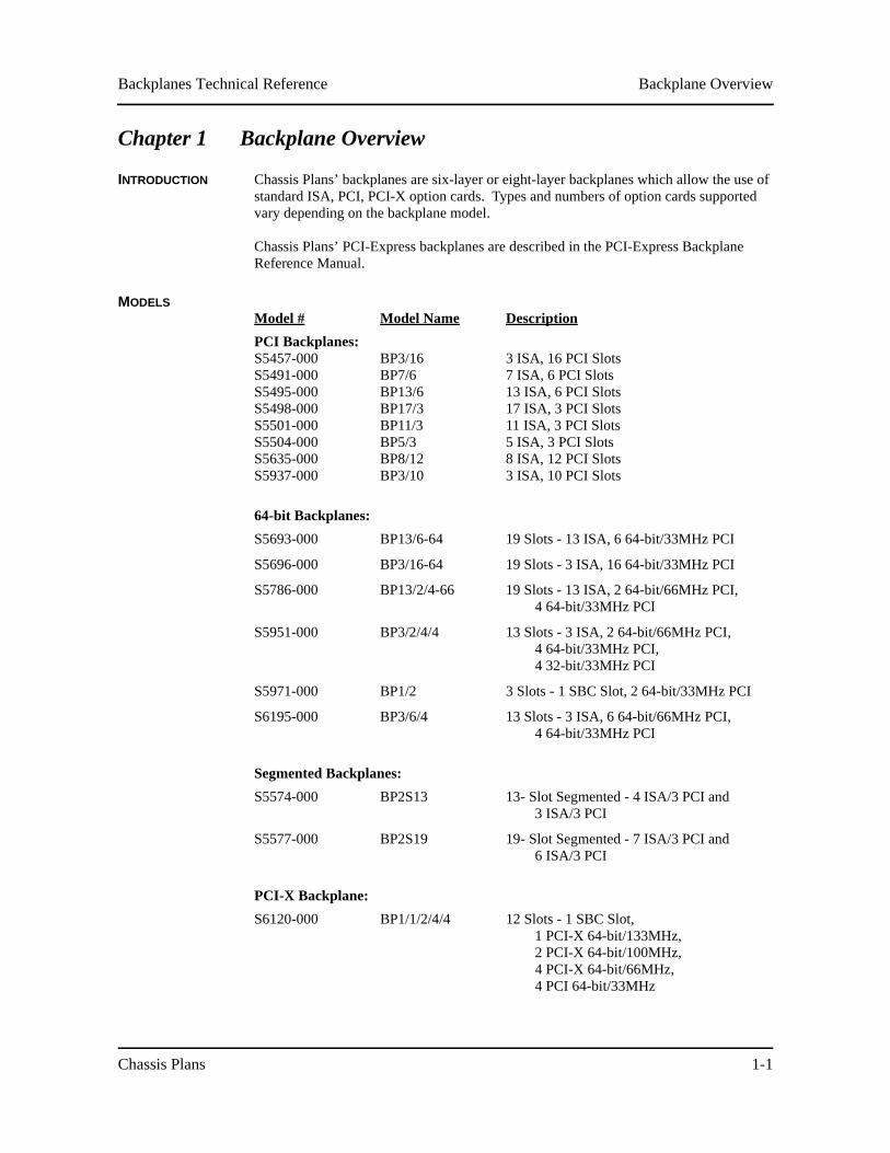
INTRODUCTION Chassis Plans’ backplanes are six-layer or eight-layer backplanes which allow the use of standard ISA, PCI, PCI-X option cards. Types and numbers of option cards supported vary depending on the backplane model.
Chassis Plans’ PCI-Express backplanes are described in the PCI-Express Backplane Reference Manual.
MODELSModel # Model Name DescriptionPCI Backplanes:S5457-000S5491-000S5495-000S5498-000S5501-000S5504-000S5635-000S5937-000
BP3/16BP7/6BP13/6BP17/3BP11/3BP5/3BP8/12BP3/10
3 ISA, 16 PCI Slots7 ISA, 6 PCI Slots13 ISA, 6 PCI Slots17 ISA, 3 PCI Slots11 ISA, 3 PCI Slots5 ISA, 3 PCI Slots8 ISA, 12 PCI Slots3 ISA, 10 PCI Slots
64-bit Backplanes:S5693-000
S5696-000
S5786-000
S5951-000
S5971-000
S6195-000
BP13/6-64
BP3/16-64
BP13/2/4-66
BP3/2/4/4
BP1/2
BP3/6/4
19 Slots - 13 ISA, 6 64-bit/33MHz PCI
19 Slots - 3 ISA, 16 64-bit/33MHz PCI
19 Slots - 13 ISA, 2 64-bit/66MHz PCI,4 64-bit/33MHz PCI
13 Slots - 3 ISA, 2 64-bit/66MHz PCI,4 64-bit/33MHz PCI, 4 32-bit/33MHz PCI
3 Slots - 1 SBC Slot, 2 64-bit/33MHz PCI
13 Slots - 3 ISA, 6 64-bit/66MHz PCI,4 64-bit/33MHz PCI
Segmented Backplanes:S5574-000
S5577-000
BP2S13
BP2S19
13- Slot Segmented - 4 ISA/3 PCI and3 ISA/3 PCI
19- Slot Segmented - 7 ISA/3 PCI and6 ISA/3 PCI
PCI-X Backplane:S6120-000 BP1/1/2/4/4 12 Slots - 1 SBC Slot,
1 PCI-X 64-bit/133MHz,2 PCI-X 64-bit/100MHz,4 PCI-X 64-bit/66MHz,4 PCI 64-bit/33MHz
Backplane Overview Backplanes Technical Reference
Chassis Plans1-2
FEATURES • Six-layer or eight-layer printed circuit board
• High noise immunity construction
• Accept single board computers (SBCs) with PCI Industrial Computer Manufac-turers Group (PICMG®) 1.0 compatible PCI Local Bus extension and standard ISA Bus SBCsl
• Allow use of standard ISA, PCI, or PCI-X option cards, depending on model
• Bus termination resistor sockets
• Standard AT, ATX, extended-current and/or EPS power connectors, depending on model
BACKPLANE OVERVIEW
Bus Architecture
The PCI/ISA backplanes allow the use of standard ISA Bus and PCI Local Bus option cards. The backplanes accept SBCs with PICMG compliant PCI Local Bus extension connectors to route the local bus signals to the standard PCI Local Bus expansion slots. The backplanes also accept standard ISA Bus SBCs. The PCI-X backplanes provide support for PCI-X and PCI option cards.
Each backplane is described individually in the following chapters of this manual.
Bus Terminations - ISA Bus
Terminations provide a method to prevent or minimize reflections and interference on the bus. If a bus is not terminated, the bus signals reach the end of the bus and reflect back down the bus. In extreme cases, these reflected signals interfere with the real bus information, leading to spurious operation or lock-ups. This can become a significant factor on the ISA Bus with option cards having non-standard load characteristics or with long ISA Bus lengths. However, provision is made for installing terminations as required by the customer's application.
The backplanes provide termination sockets at the left end of the bus for the ISA Bus.
Terminations connect the bus to +5V and ground, providing a path for the bus signals to dissipate. A terminated bus provides signals with less noise, but the rise and fall times are slower. However, this is highly dependent on the SBC and option cards and must be evaluated on a case-by-case basis.
The sockets provided on the backplane accept standard 10-position SIPs manufactured by Bourns and others. Signals and corresponding termination connections are listed later in this chapter.
Backplane OverviewBackplanes Technical Reference
Chassis Plans 1-3
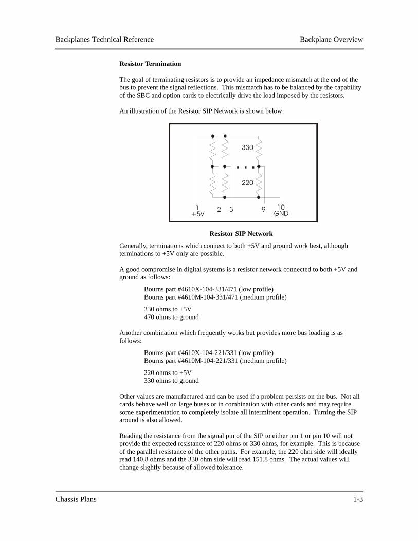
Resistor Termination
The goal of terminating resistors is to provide an impedance mismatch at the end of the bus to prevent the signal reflections. This mismatch has to be balanced by the capability of the SBC and option cards to electrically drive the load imposed by the resistors.
An illustration of the Resistor SIP Network is shown below:
Resistor SIP Network
Generally, terminations which connect to both +5V and ground work best, although terminations to +5V only are possible.
A good compromise in digital systems is a resistor network connected to both +5V and ground as follows:
Bourns part #4610X-104-331/471 (low profile)Bourns part #4610M-104-331/471 (medium profile)
330 ohms to +5V470 ohms to ground
Another combination which frequently works but provides more bus loading is as follows:
Bourns part #4610X-104-221/331 (low profile)Bourns part #4610M-104-221/331 (medium profile)
220 ohms to +5V330 ohms to ground
Other values are manufactured and can be used if a problem persists on the bus. Not all cards behave well on large buses or in combination with other cards and may require some experimentation to completely isolate all intermittent operation. Turning the SIP around is also allowed.
Reading the resistance from the signal pin of the SIP to either pin 1 or pin 10 will not provide the expected resistance of 220 ohms or 330 ohms, for example. This is because of the parallel resistance of the other paths. For example, the 220 ohm side will ideally read 140.8 ohms and the 330 ohm side will read 151.8 ohms. The actual values will change slightly because of allowed tolerance.
Backplane Overview Backplanes Technical Reference
Chassis Plans1-4
Keyboard Connectors
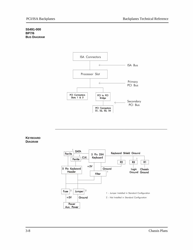
For those backplanes with keyboard connectors, there are three keyboard connectors connected in parallel on the backplanes. Two are 5-pin headers and one is a standard AT 5-pin DIN connector. One of the two 5-pin headers may be used to bring keyboard signals from the SBC to the backplane and the other to provide a front-mounted keyboard connector. The 5-pin DIN provides a standard back panel connector. In addition, provision has been made for optional filtering for the 5-pin DIN connector when necessary. (Refer to the backplane block diagrams in the following chapters of this manual.)
Power Supply Connectors
Many backplanes have multiple power supply connectors. On these backplanes, the +5V connections are generally common, as are all of the +12V, -12V, +5V and ground connections. Power may be connected via any of the connectors, as long as all four voltages are delivered to the system.
Chassis Plans backplanes provide +3.3V power supply connections for PCI peripheral cards which require +3.3V of DC power. Chassis Plans SBCs do not require +3.3 volts from the power supply because they have their own VRMs on board. The +3.3V power supply connections do not power the processor slot on these backplanes.
Some models provide optional ATX, extended-current or EPS power connectors. Refer to the backplane descriptions in the following chapters of this manual for more infor-mation about a specific backplane.
Backplane OverviewBackplanes Technical Reference
Chassis Plans 1-5
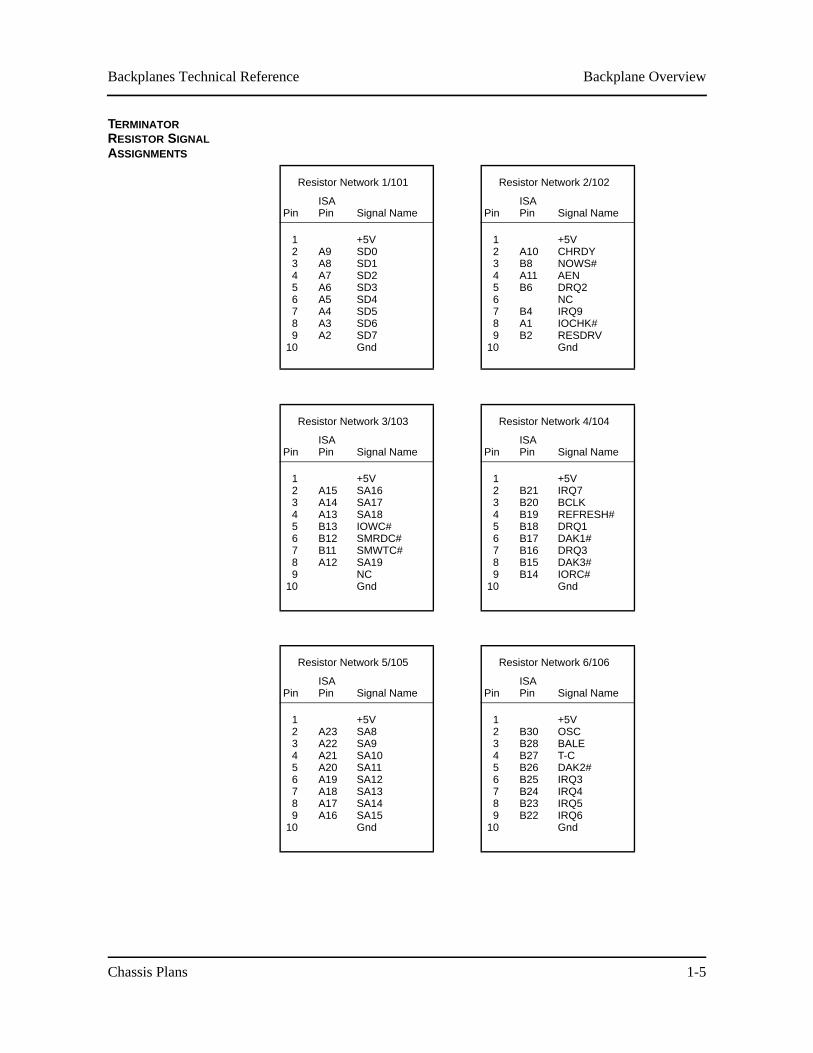
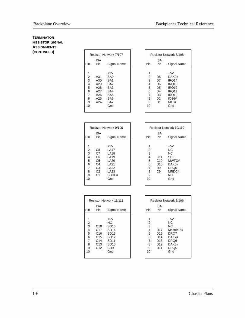
TERMINATOR RESISTOR SIGNAL ASSIGNMENTS
Resistor Network 1/101 Resistor Network 2/102
PinISAPin Signal Name Pin
ISAPin Signal Name
123456789
10
A9A8A7A6A5A4A3A2
+5VSD0SD1SD2SD3SD4SD5SD6SD7Gnd
123456789
10
A10B8A11B6
B4A1B2
+5VCHRDYNOWS#AENDRQ2NCIRQ9IOCHK#RESDRVGnd
Resistor Network 3/103 Resistor Network 4/104
PinISAPin Signal Name Pin
ISAPin Signal Name
123456789
10
A15A14A13B13B12B11A12
+5VSA16SA17SA18IOWC#SMRDC#SMWTC#SA19NCGnd
123456789
10
B21B20B19B18B17B16B15B14
+5VIRQ7BCLKREFRESH#DRQ1DAK1#DRQ3DAK3#IORC#Gnd
Resistor Network 5/105 Resistor Network 6/106
PinISAPin Signal Name Pin
ISAPin Signal Name
123456789
10
A23A22A21A20A19A18A17A16
+5VSA8SA9SA10SA11SA12SA13SA14SA15Gnd
123456789
10
B30B28B27B26B25B24B23B22
+5VOSCBALET-CDAK2#IRQ3IRQ4IRQ5IRQ6Gnd
Backplane Overview Backplanes Technical Reference
Chassis Plans1-6
TERMINATOR RESISTOR SIGNAL ASSIGNMENTS (CONTINUED)
Copyright 2006 by Trenton Technology Inc. All rights reserved.
Resistor Network 7/107 Resistor Network 8/108
PinISAPin Signal Name Pin
ISAPin Signal Name
123456789
10
A31A30A29A28A27A26A25A24
+5VSA0SA1SA2SA3SA4SA5SA6SA7Gnd
123456789
10
D8D7D6D5D4D3D2D1
+5VDAK0#IRQ14IRQ15IRQ12IRQ11IRQ10IO16#M16#Gnd
Resistor Network 9/109 Resistor Network 10/110
PinISAPin Signal Name Pin
ISAPin Signal Name
123456789
10
C8C7C6C5C4C3C2C1
+5VLA17LA18LA19LA20LA21LA22LA23SBHE#Gnd
123456789
10
C11C10D10D9C9
+5VNCNCSD8MWTC#DAK5#DRQ0MRDC#NCGnd
Resistor Network 11/111 Resistor Network 6/106
PinISAPin Signal Name Pin
ISAPin Signal Name
123456789
10
C18C17C16C15C14C13C12
+5VNCSD15SD14SD13SD12SD11SD10SD9Gnd
123456789
10
D17D15D14D13D12D11
+5VNCNCMaster16#DRQ7DAK7#DRQ6DAK6#DRQ5Gnd
ISA/PCI ReferenceBackplanes Technical Reference
Chassis Plans 2-1
Chapter 2 ISA/PCI Reference
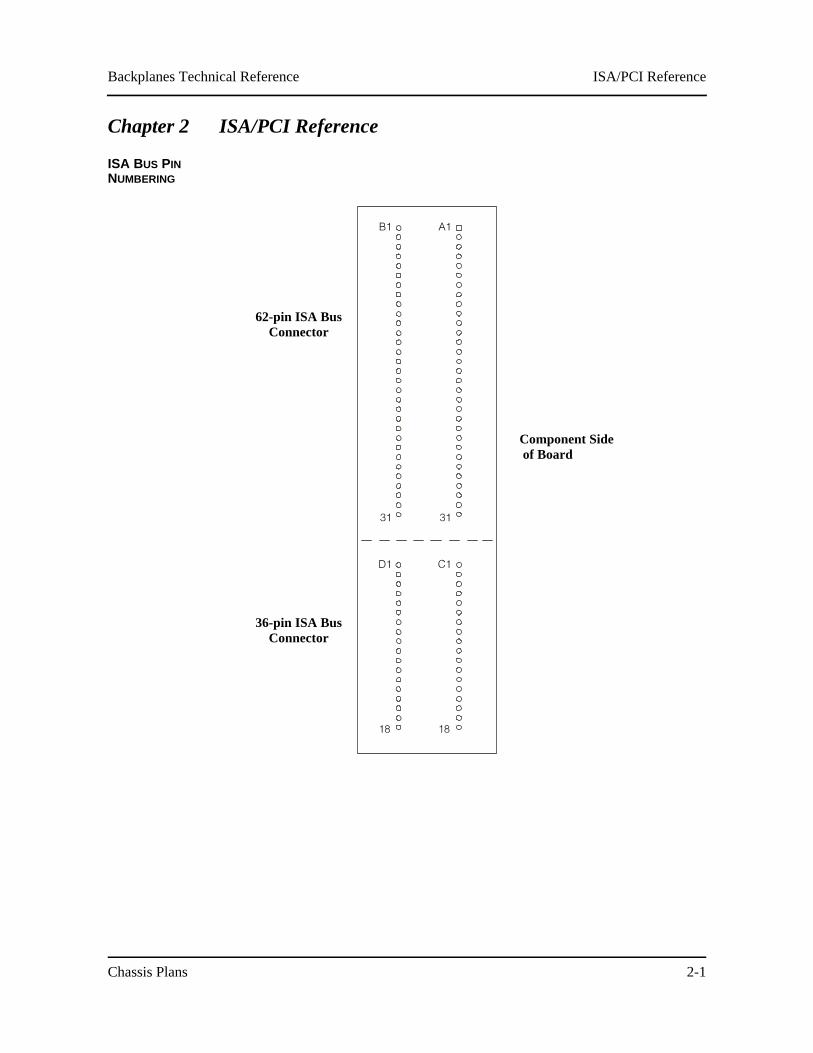
ISA BUS PIN NUMBERING
62-pin ISA Bus Connector
Component Side of Board
36-pin ISA Bus Connector
ISA/PCI Reference Backplanes Technical Reference
Chassis Plans2-2
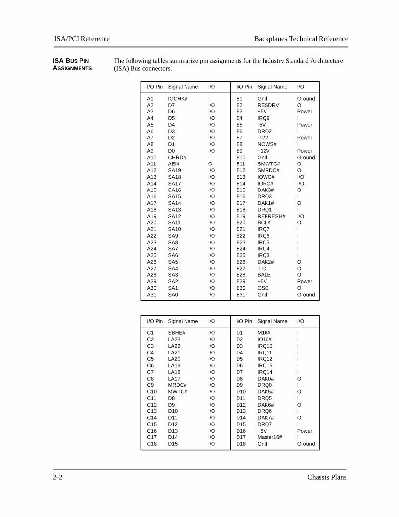
ISA BUS PIN ASSIGNMENTS
The following tables summarize pin assignments for the Industry Standard Architecture (ISA) Bus connectors.
I/O Pin Signal Name I/O I/O Pin Signal Name I/O
A1A2A3A4A5A6A7A8A9A10A11A12A13A14A15A16A17A18A19A20A21A22A23A24A25A26A27A28A29A30A31
IOCHK#D7D6D5D4D3D2D1D0CHRDYAENSA19SA18SA17SA16SA15SA14SA13SA12SA11SA10SA9SA8SA7SA6SA5SA4SA3SA2SA1SA0
II/OI/OI/OI/OI/OI/OI/OI/OIOI/OI/OI/OI/OI/OI/OI/OI/OI/OI/OI/OI/OI/OI/OI/OI/OI/OI/OI/OI/O
B1B2B3B4B5B6B7B8B9B10B11B12B13B14B15B16B17B18B19B20B21B22B23B24B25B26B27B28B29B30B31
GndRESDRV+5VIRQ9-5VDRQ2-12VNOWS#+12VGndSMWTC#SMRDC#IOWC#IORC#DAK3#DRQ3DAK1#DRQ1REFRESH#BCLKIRQ7IRQ6IRQ5IRQ4IRQ3DAK2#T-CBALE+5VOSCGnd
GroundOPowerIPowerIPowerIPowerGroundOOI/OI/OOIOII/OOIIIIIOOOPowerOGround
I/O Pin Signal Name I/O I/O Pin Signal Name I/O
C1C2C3C4C5C6C7C8C9C10C11C12C13C14C15C16C17C18
SBHE#LA23LA22LA21LA20LA19LA18LA17MRDC#MWTC#D8D9D10D11D12D13D14D15
I/OI/OI/OI/OI/OI/OI/OI/OI/OI/OI/OI/OI/OI/OI/OI/OI/OI/O
D1D2D3D4D5D6D7D8D9D10D11D12D13D14D15D16D17D18
M16#IO16#IRQ10IRQ11IRQ12IRQ15IRQ14DAK0#DRQ0DAK5#DRQ5DAK6#DRQ6DAK7#DRQ7+5VMaster16#Gnd
IIIIIIIOIOIOIOIPowerIGround
ISA/PCI ReferenceBackplanes Technical Reference
Chassis Plans 2-3
ISA BUS SIGNAL DESCRIPTIONS
The following is a description of the ISA Bus signals. All signal lines are TTL-compatible.
AEN (O)
Address Enable (AEN) is used to degate the microprocessor and other devices from the I/O channel to allow DMA transfers to take place. When this line is active, the DMA controller has control of the address bus, the data-bus Read command lines (memory and I/O), and the Write command lines (memory and I/O).
BALE (O) (Buffered)
Address Latch Enable (BALE) is provided by the bus controller and is used on the system board to latch valid addresses and memory decodes from the microprocessor. It is available to the I/O channel as an indicator of a valid microprocessor or DMA address (when used with AEN). Microprocessor addresses SA[19::0] are latched with the falling edge of BALE. BALE is forced high during DMA cycles.
BCLK (O)
BCLK is the system clock. The clock has a 50% duty cycle. This signal should only be used for synchronization. It is not intended for uses requiring a fixed frequency.
CHRDY (I)
I/O Channel Ready (CHRDY) is pulled low (not ready) by a memory or I/O device to lengthen I/O or memory cycles. Any slow device using this line should drive it low immediately upon detecting its valid address and a Read or Write command. Machine cycles are extended by an integral number of clock cycles. This signal should be held low for no more than 2.5 micro-seconds.
D[15::0] (I/O)
Data signals D[15::0] provide bus bits 15 through 0 for the microprocessor, memory, and I/O devices. D15 is the most-significant bit and D0 is the least-significant bit. All 8-bit devices on the I/O channel should use D[7::0] for communications to the microprocessor. The 16-bit devices will use D[15::0]. To support 8-bit devices, the data on D[15::8] will be gated to D[7::0] during 8-bit transfers to these devices. 16-bit microprocessor transfers to 8-bit devices will be converted to two 8-bit transfers.
DAK[7::5]#, DAK[3::0]# (O)
DMA Acknowledge DAK[7::5]# and DAK[3::0]# are used to acknowledge DMA requests DRQ[7::5] and DRQ[3::0]. They are active low.
DRQ[7::5], DRQ[3::0] (I)
DMA Requests DRQ[7::5] and DRQ[3::0] are asynchronous channel requests used by peripheral devices and the I/O channel microprocessors to gain DMA service (or control of the system). They are prioritized, with DRQ0 having the highest priority and DRQ7 having the lowest. A request is generated by bringing a DRQ line to an active level. A DRQ line must be held high until the corresponding DMA Request Acknowledge (DAK) line goes active. DRQ[3::0] will perform 8-bit DMA transfers; DRQ[7::5] will perform 16-bit transfers.
ISA/PCI Reference Backplanes Technical Reference
Chassis Plans2-4
IO16# (I)
I/O 16-bit Chip Select (IO16#) signals the system board that the present data transfer is a 16-bit, 1 wait-state, I/O cycle. It is derived from an address decode. IO16# is active low and should be driven with an open collector or tri-state driver capable of sinking 20 mAmps.
IOCHK# (I)
I/O Channel Check (IOCHK#) provides the system board with parity (error) information about memory or devices on the I/O channel. When this signal is active, it indicates an uncorrectable system error.
IORC# (I/O)
I/O Read (IORC#) instructs an I/O device to drive its data onto the data bus. It may be driven by the system microprocessor or DMA controller, or by a microprocessor or DMA controller resident on the I/O channel. This signal is active low.
IOWC# (I/O)
I/O Write (IOWC#) instructs an I/O device to read the data on the data bus. It may be driven by any microprocessor or DMA controller in the system. This signal is active low.
IRQ[15::14], IRQ[12::9], IRQ[7::3] (I)
Interrupt Requests IRQ[15::14], IRQ[12::9] and IRQ[7::3] are used to signal the microprocessor that an I/O device needs attention. The interrupt requests are prioritized, with IRQ[15::14] and IRQ[12::9] having the highest priority (IRQ9 is the highest) and IRQ[7::3] having the lowest priority (IRQ7 is the lowest). An interrupt request is generated when an IRQ line is raised from low to high. The line must be held high until the microprocessor acknowledges the interrupt request (Interrupt Service routine).
LA[23::17] (I/O)
These signals (unlatched) are used to address memory and I/O devices within the system. They give the system up to 16MB of addressability. These signals are valid when BALE is high. LA[23::17] are not latched during microprocessor cycles and therefore do not stay valid for the whole cycle. Their purpose is to generate memory decodes for 1 wait-state memory cycles. These decodes should be latched by I/O adapters on the falling edge of BALE. These signals also may be driven by other microprocessors or DMA controllers that reside on the I/O channel.
M16# (I)
M16# Chip Select signals the system board if the present data transfer is a 1<N>wait-state, 16-bit, memory cycle. It must be derived from the decode of LA[23::17]. M16# should be driven with an open collector or tri-state driver capable of sinking 20 mAmps.
Master16# (I)
Master16# is used with a DRQ line to gain control of the system. A processor or DMA controller on the I/O channel may issue a DRQ to a DMA channel in cascade mode and receive a DAK#. Upon receiving the DAK#, an I/O microprocessor may pull Master16# low, which will allow it to control the system address, data, and control lines (a condition known as tri-state). After Master16# is low, the I/O microprocessor must wait one system clock period before driving the address and data lines, and two clock periods before issuing a Read or Write command. If this signal is held low for more than 15<N>microseconds, system memory may be lost because of a lack of refresh.
ISA/PCI ReferenceBackplanes Technical Reference
Chassis Plans 2-5
NOWS# (I)
The No Wait State (NOWS#) signal tells the microprocessor that it can complete the present bus cycle without inserting any additional wait cycles. In order to run a memory cycle to a 16-bit device without wait cycles, NOWS# is derived from an address decode gated with a Read or Write command. In order to run a memory cycle to an 8-bit device with a minimum of two wait states, NOWS# should be driven active on system clock after the Read or Write command is active gated with the address decode for the device. Memory Read and Write commands to a 8-bit device are active on the falling edge of the system clock. NOWS# is active low and should be driven with an open collector or tri-state driver capable of sinking 20 mAmps.
OSC (O)
Oscillator (OSC) is a high-speed clock with a 70-nanosecond period (14.31818 MHz). This signal is not synchronous with the system clock. It has a 50% duty cycle.
REFRESH# (I/O)
The REFRESH# signal is used to indicate a refresh cycle and can be driven by a micropro-cessor on the I/O channel.
RESDRV (O)
Reset Drive (RESDRV) is used to reset or initialize system logic at power-up time or during a low line-voltage outage. This signal is active high.
SA[19::0] (I/O)
Address bits SA[19::0] are used to address memory and I/O devices within the system. These twenty address lines, in addition to LA[23::17], allow access of up to 16MB of memory. SA[19::0] are gated on the system bus when BALE is high and are latched on the falling edge of BALE. These signals are generated by the microprocessor or DMA Controller. They also may be driven by other microprocessors or DMA controllers that reside on the I/O channel.
SBHE# (I/O)
System Bus High Enable (SBHE#) indicates a transfer of data on the upper byte of the data bus, D[15::8]. 16-bit devices use SBHE# to condition data bus buffers tied to D[15::8].
SMRDC# (O), MRDC# (I/O)
These signals instruct the memory devices to drive data onto the data bus. SMRDC# is active only when the memory decode is within the low 1MB of memory space. MRDC# is active on all memory read cycles. MRDC# may be driven by any microprocessor or DMA controller in the system. SMRDC is derived from MRDC# and the decode of the low 1MB of memory. When a microprocessor on the I/O channel wishes to drive MRDC#, it must have the address lines valid on the bus for one system clock period before driving MRDC# active. Both signals are active low.
SMWTC# (O), MWTC# (I/O)
These signals instruct the memory devices to store the data present on the data bus. SMWTC# is active only when the memory decode is within the low 1MB of the memory space. MWTC# is active on all memory write cycles. MWTC# may be driven by any microprocessor or DMA controller in the system. SMWTC# is derived from MWTC# and the decode of the low 1MB of memory. When a microprocessor on the I/O channel wishes to drive MWTC#, it must have the address lines valid on the bus for one system clock period before driving MWTC# active. Both signals are active low.

ISA/PCI Reference Backplanes Technical Reference
Chassis Plans2-6
T-C (O)
Terminal Count (T-C) provides a pulse when the terminal count for any DMA channel is reached.
ISA/PCI ReferenceBackplanes Technical Reference
Chassis Plans 2-7
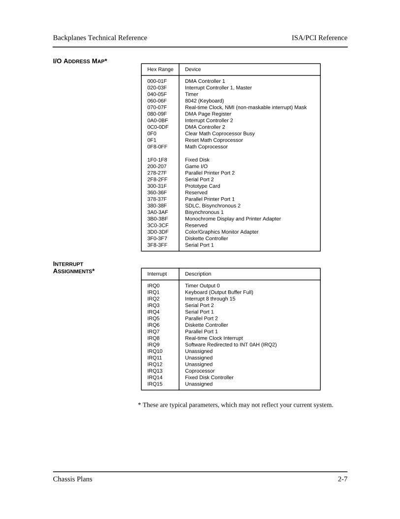
I/O ADDRESS MAP*
INTERRUPT ASSIGNMENTS*
* These are typical parameters, which may not reflect your current system.
Hex Range Device
000-01F020-03F040-05F060-06F070-07F080-09F0A0-0BF0C0-0DF0F00F10F8-0FF
1F0-1F8200-207278-27F2F8-2FF300-31F360-36F378-37F380-38F3A0-3AF3B0-3BF3C0-3CF3D0-3DF3F0-3F73F8-3FF
DMA Controller 1Interrupt Controller 1, MasterTimer8042 (Keyboard)Real-time Clock, NMI (non-maskable interrupt) MaskDMA Page RegisterInterrupt Controller 2DMA Controller 2Clear Math Coprocessor BusyReset Math CoprocessorMath Coprocessor
Fixed DiskGame I/OParallel Printer Port 2Serial Port 2Prototype CardReservedParallel Printer Port 1SDLC, Bisynchronous 2Bisynchronous 1Monochrome Display and Printer AdapterReservedColor/Graphics Monitor AdapterDiskette ControllerSerial Port 1
Interrupt Description
IRQ0IRQ1IRQ2IRQ3IRQ4IRQ5IRQ6IRQ7IRQ8IRQ9IRQ10IRQ11IRQ12IRQ13IRQ14IRQ15
Timer Output 0Keyboard (Output Buffer Full)Interrupt 8 through 15Serial Port 2Serial Port 1Parallel Port 2Diskette ControllerParallel Port 1Real-time Clock InterruptSoftware Redirected to INT 0AH (IRQ2)UnassignedUnassignedUnassignedCoprocessorFixed Disk ControllerUnassigned
ISA/PCI Reference Backplanes Technical Reference
Chassis Plans2-8
PCI LOCAL BUS OVERVIEW
The PCI (Peripheral Component Interconnect) Local Bus is a high performance, 32-bit or 64-bit bus with multiplexed address and data lines. It is intended for use as an inter-connect mechanism between highly integrated peripheral controller components, peripheral add-in boards and processor/memory systems.
The "local bus" moves peripheral functions with high bandwidth requirements closer to the system’s processor bus and can produce substantial performance gains with graphical user interfaces (GUIs) and other high bandwidth functions (i.e., full motion video, SCSI, LANs, etc.).
The PCI Local Bus accommodates future system requirements and is applicable across multiple platforms and architectures.
The PCI component and add-in card interface is processor independent, enabling an efficient transition to future processor generations, by bridges or by direct integration, and use with multiple processor architectures. Processor independence allows the PCI Local Bus to be optimized for I/O functions, enables concurrent operation of the local bus with the processor/memory subsystem, and accommodates multiple high perfor-mance peripherals in addition to graphics. Movement to enhanced video and multimedia displays and other high bandwidth I/O will continue to increase local bus bandwidth requirements. A transparent 64-bit extension of the 32-bit data and address buses is defined, doubling the bus bandwidth and offering forward and backward compatibility of 32-bit (132MB/s peak) and 64-bit (264MB/s peak) PCI Local Bus peripherals.
ISA/PCI ReferenceBackplanes Technical Reference
Chassis Plans 2-9
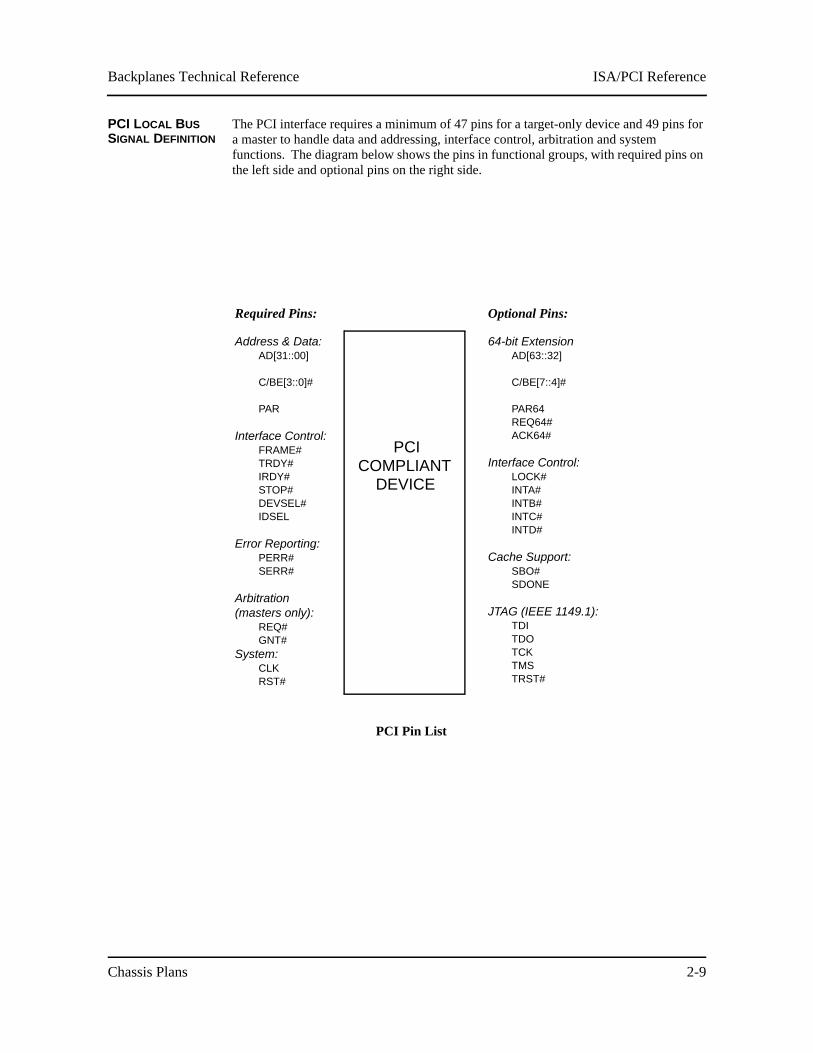
PCI LOCAL BUS SIGNAL DEFINITION
The PCI interface requires a minimum of 47 pins for a target-only device and 49 pins for a master to handle data and addressing, interface control, arbitration and system functions. The diagram below shows the pins in functional groups, with required pins on the left side and optional pins on the right side.
PCI Pin List
Required Pins:
Address & Data:AD[31::00]
C/BE[3::0]#
PAR
Interface Control:FRAME#TRDY#IRDY#STOP#DEVSEL#IDSEL
Error Reporting:PERR#SERR#
Arbitration(masters only):
REQ#GNT#
System:CLKRST#
Optional Pins:
64-bit ExtensionAD[63::32]
C/BE[7::4]#
PAR64REQ64#ACK64#
Interface Control:LOCK#INTA#INTB#INTC#INTD#
Cache Support:SBO#SDONE
JTAG (IEEE 1149.1):TDITDOTCKTMSTRST#
PCICOMPLIANT
DEVICE
ISA/PCI Reference Backplanes Technical Reference
Chassis Plans2-10
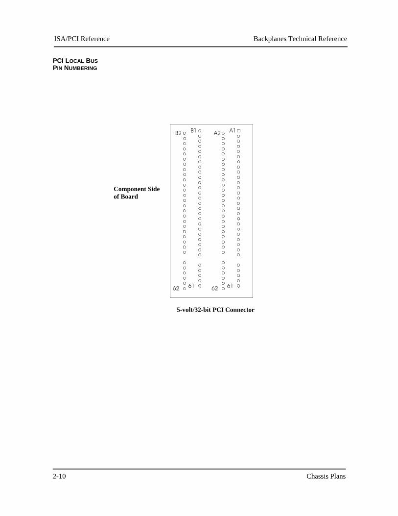
PCI LOCAL BUS PIN NUMBERING
Component Sideof Board
5-volt/32-bit PCI Connector
ISA/PCI ReferenceBackplanes Technical Reference
Chassis Plans 2-11
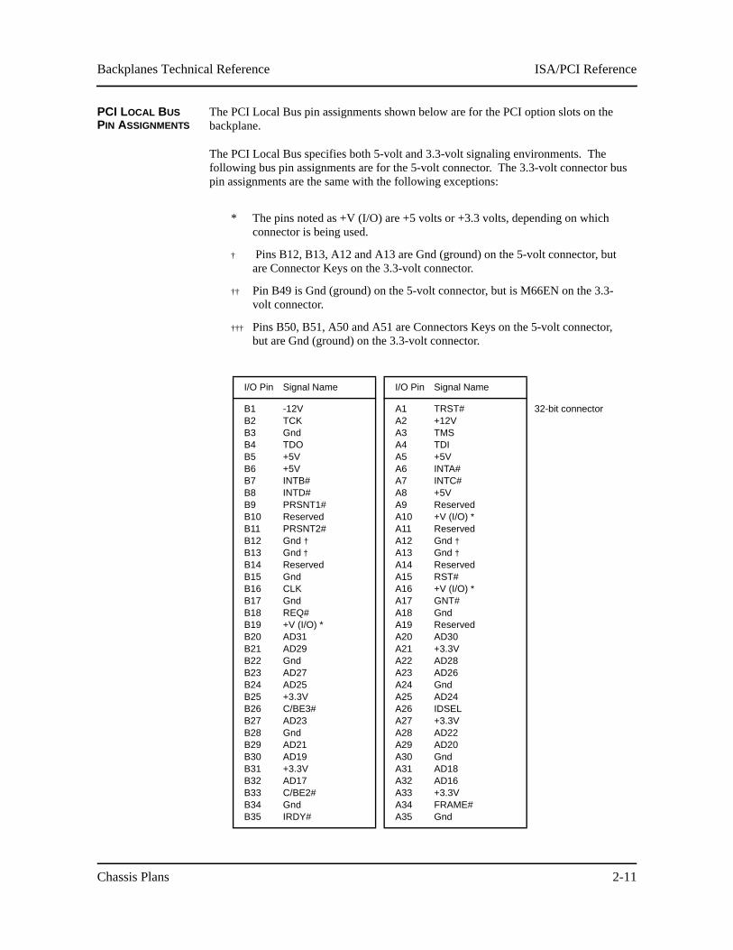
PCI LOCAL BUS PIN ASSIGNMENTS
The PCI Local Bus pin assignments shown below are for the PCI option slots on the backplane.
The PCI Local Bus specifies both 5-volt and 3.3-volt signaling environments. The following bus pin assignments are for the 5-volt connector. The 3.3-volt connector bus pin assignments are the same with the following exceptions:
* The pins noted as +V (I/O) are +5 volts or +3.3 volts, depending on which connector is being used.
† Pins B12, B13, A12 and A13 are Gnd (ground) on the 5-volt connector, but are Connector Keys on the 3.3-volt connector.
†† Pin B49 is Gnd (ground) on the 5-volt connector, but is M66EN on the 3.3-volt connector.
††† Pins B50, B51, A50 and A51 are Connectors Keys on the 5-volt connector, but are Gnd (ground) on the 3.3-volt connector.
I/O Pin Signal Name I/O Pin Signal Name
B1B2B3B4B5B6B7B8B9B10B11B12B13B14B15B16B17B18B19B20B21B22B23B24B25B26B27B28B29B30B31B32B33B34B35
-12VTCKGndTDO+5V+5VINTB#INTD#PRSNT1#ReservedPRSNT2#Gnd †Gnd †ReservedGndCLKGndREQ#+V (I/O) *AD31AD29GndAD27AD25+3.3VC/BE3#AD23GndAD21AD19+3.3VAD17C/BE2#GndIRDY#
A1A2A3A4A5A6A7A8A9A10A11A12A13A14A15A16A17A18A19A20A21A22A23A24A25A26A27A28A29A30A31A32A33A34A35
TRST#+12VTMSTDI+5VINTA#INTC#+5VReserved+V (I/O) *ReservedGnd †Gnd †ReservedRST#+V (I/O) *GNT#GndReservedAD30+3.3VAD28AD26GndAD24IDSEL+3.3VAD22AD20GndAD18AD16+3.3VFRAME#Gnd
32-bit connector
ISA/PCI Reference Backplanes Technical Reference
Chassis Plans2-12
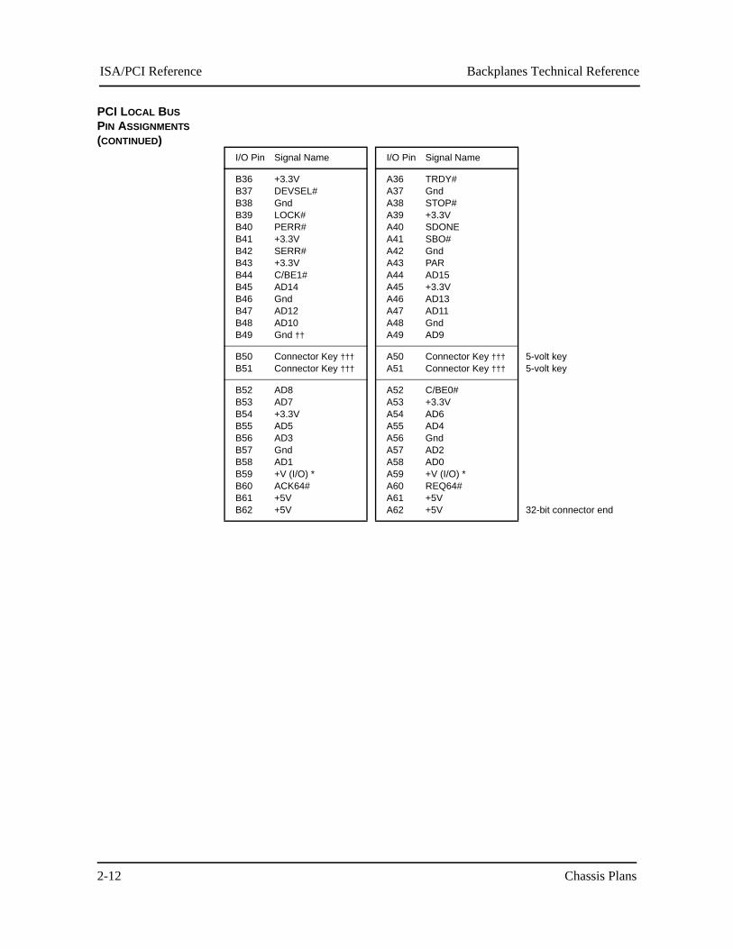
PCI LOCAL BUS PIN ASSIGNMENTS (CONTINUED)
I/O Pin Signal Name I/O Pin Signal Name
B36B37B38B39B40B41B42B43B44B45B46B47B48B49
+3.3VDEVSEL#GndLOCK#PERR#+3.3VSERR#+3.3VC/BE1#AD14GndAD12AD10Gnd ††
A36A37A38A39A40A41A42A43A44A45A46A47A48A49
TRDY#GndSTOP#+3.3VSDONESBO#GndPARAD15+3.3VAD13AD11GndAD9
B50B51
Connector Key †††Connector Key †††
A50A51
Connector Key †††Connector Key †††
5-volt key5-volt key
B52B53B54B55B56B57B58B59B60B61B62
AD8AD7+3.3VAD5AD3GndAD1+V (I/O) *ACK64#+5V+5V
A52A53A54A55A56A57A58A59A60A61A62
C/BE0#+3.3VAD6AD4GndAD2AD0+V (I/O) *REQ64#+5V+5V 32-bit connector end
ISA/PCI ReferenceBackplanes Technical Reference
Chassis Plans 2-13
PCI LOCAL BUS PIN ASSIGNMENTS (CONTINUED)
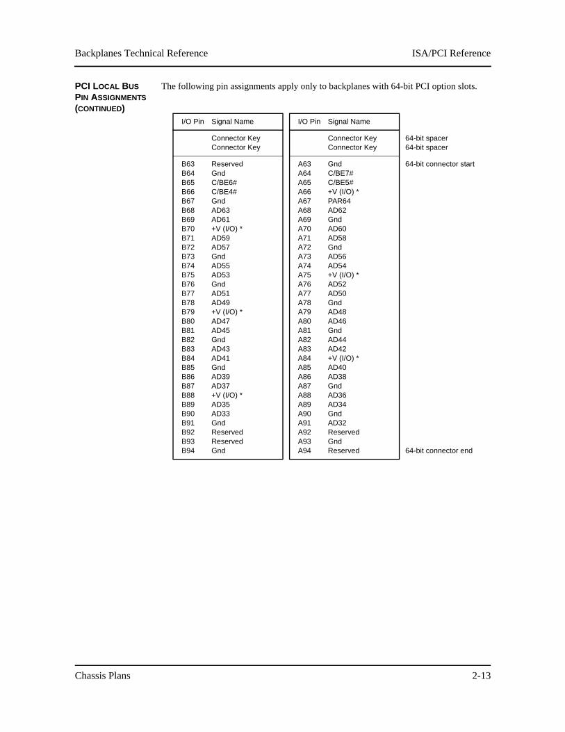
The following pin assignments apply only to backplanes with 64-bit PCI option slots.
I/O Pin Signal Name I/O Pin Signal Name
Connector KeyConnector Key
Connector KeyConnector Key
64-bit spacer64-bit spacer
B63B64B65B66B67B68B69B70B71B72B73B74B75B76B77B78B79B80B81B82B83B84B85B86B87B88B89B90B91B92B93B94
ReservedGndC/BE6#C/BE4#GndAD63AD61+V (I/O) *AD59AD57GndAD55AD53GndAD51AD49+V (I/O) *AD47AD45GndAD43AD41GndAD39AD37+V (I/O) *AD35AD33GndReservedReservedGnd
A63A64A65A66A67A68A69A70A71A72A73A74A75A76A77A78A79A80A81A82A83A84A85A86A87A88A89A90A91A92A93A94
GndC/BE7#C/BE5#+V (I/O) *PAR64AD62GndAD60AD58GndAD56AD54+V (I/O) *AD52AD50GndAD48AD46GndAD44AD42+V (I/O) *AD40AD38GndAD36AD34GndAD32ReservedGndReserved
64-bit connector start
64-bit connector end
ISA/PCI Reference Backplanes Technical Reference
Chassis Plans2-14
PCI LOCAL BUS SIGNAL DESCRIPTIONS
The PCI Local Bus signals are described below and may be categorized into the following functional groups:
• System Pins
• Address and Data Pins
• Interface Control Pins
• Arbitration Pins (Bus Masters Only)
• Error Reporting Pins
• Interrupt Pins (Optional)
• Cache Support Pins (Optional)
• 64-Bit Bus Extension Pins (Optional)
• JTAG/Boundary Scan Pins (Optional)
A # symbol at the end of a signal name indicates that the active state occurs when the signal is at a low voltage. When the # symbol is absent, the signal is active at a high voltage.
The following are descriptions of the PCI Local Bus signals.
ACK64# (optional)
Acknowledge 64-bit Transfer, when actively driven by the device that has positively decoded its address as the target of the current access, indicates the target is willing to transfer data using 64bits. ACK64# has the same timing as DEVSEL#.
AD[31::00]
Address and Data are multiplexed on the same PCI pins. A bus transaction consists of an address phase followed by one or more data phases. During the address phase, AD[31::00] contain a physical address (32 bits). During data phases, AD[07::00] contain the least signif-icant byte (lsb) and AD[31::24] contain the most significant byte (msb).
AD[63::32] (optional)
Address and Data are multiplexed on the same pins and provide 32additional bits. During an address phase (when using the DAC command and when REQ64# is asserted), the upper 32bits of a 64-bit address are transferred; otherwise, these bits are reserved but are stable and indeterminate. During a data phase, an additional 32bits of data are transferred when REQ64# and ACK64# are both asserted.
C/BE[3::0]#
Bus Command and Byte Enables are multiplexed on the same PCI pins. During the address phase of a transaction, these pins define the bus command; during the data phase they are used as byte enables. The byte enables are valid for the entire data phase and determine which byte lanes carry meaningful data. C/BE0# applies to byte0 (lsb) and C/BE3# applies to byte 3 (msb).
ISA/PCI ReferenceBackplanes Technical Reference
Chassis Plans 2-15
C/BE[7::4]# (optional)
Bus Command and Byte Enables are multiplexed on the same pins. During an address phase (when using the DAC command and when REQ64# is asserted), the actual bus command is transferred on C/BE[7::4]#; otherwise, these bits are reserved and indeterminate. During a data phase, C/BE[7::4]# are byte enables indicating which byte lanes carry meaningful data when REQ64# and ACK64# are both asserted. C/BE4# applies to byte4 and C/BE7# applies to byte7.
CLK
Clock provides timing for all transactions on PCI and is an input to every PCI device.
DEVSEL#
Device Select, when actively driven, indicates that the driving device has decoded its address as the target of the current access. As an input, DEVSEL# indicates whether any device on the bus has been selected.
FRAME#
Cycle Frame is an interface control pin which is driven by the current master to indicate the beginning and duration of an access. When FRAME# is asserted, data transfers continue; when it is deasserted, the transaction is in the final data phase.
GNT#
Grant indicates to the agent that access to the bus has been granted. This is a point to point signal. Every master has its own GNT#.
IDSEL
Initialization Device Select is used as a chip select during configuration read and write transac-tions.
INTA#, INTB#, INTC#, INTD# (optional)
Interrupts on PCI are optional and defined as "level sensitive," asserted low (negative true), using open drain output drivers. PCI defines one interrupt for a single function and up to four interrupt lines for a multi-function device or connector.
Interrupt A is used to request an interrupt. For a single function device, only INTA# may be used, while the other three interrupt lines have no meaning.
Interrupt B, Interrupt C and Interrupt D are used to request additional interrupts and only have meaning on a multi-function device.
IRDY#
Initiator Ready indicates the initiating agent’s (bus master’s) ability to complete the current data phase of the transaction. IRDY# is used in conjunction with TRDY#. During a write, IRDY# indicates that valid data is present on AD[31::0]. During a read, it indicates that the master is prepared to accept data.
LOCK#
Lock indicates an operation that may require multiple transactions to complete. When LOCK# is asserted, non-exclusive transactions may proceed to an address that is not currently locked.
ISA/PCI Reference Backplanes Technical Reference
Chassis Plans2-16
PAR
Parity is even parity across AD[31::00] and C/BE[3::0]#. Parity generation is required by all PCI agents. The master drives PAR for address and write data phases; the target drives PAR for read data phases.
PAR64 (optional)
Parity Upper DWORD is the even parity bit that protects AD[63::32] and C/BE[7::4]#. The master drives PAR64 for address and write data phases; the target drives PAR64 for read data phases.
PERR#
Parity Error is for the reporting of data parity errors during all PCI transactions except a Special Cycle. There are no special conditions when a data parity error may be lost or when reporting of an error may be delayed.
PRSNT1# and PRSNT2#
PRSNT1# and PRSNT2# are related to the connector only, not to other PCI components. They are used for two purposes: indicating that a board is physically present in the slot and providing information about the total power requirements of the board.
REQ#
Request indicates to the arbiter that this agent desires use of the bus. This is a point to point signal. Every master has its own REQ#.
REQ64# (optional)
Request 64-bit Transfer, when actively driven by the current bus master, indicates it desires to transfer data using 64 bits. REQ64# has the same timing as FRAME#. REQ64# has meaning at the end of reset.
RST#
Reset is used to bring PCI-specific registers, sequencers and signals to a consistent state.
SBO# (optional)
Snoop Backoff is an optional cache support pin which indicates a hit to a modified line when asserted. When SBO# is deasserted and SDONE is asserted, it indicates a "clean" snoop result.
SDONE (optional)
Snoop Done is an optional cache support pin which indicates the status of the snoop for the current access. When deasserted, it indicates the result of the snoop is still pending. When asserted, it indicates the snoop is complete.
SERR#
System Error is for reporting address parity errors, data parity errors on the Special Cycle command, or any other system error where the result will be catastrophic. If an agent does not want a non-maskable interrupt (NMI) to be generated, a different reporting mechanism is required.
ISA/PCI ReferenceBackplanes Technical Reference
Chassis Plans 2-17
STOP#
Stop indicates that the current target is requesting the master to stop the current transaction.
TCK (optional)
Test Clock is used to clock state information and test data into and out of the device during operation of the TAP (Test Access Port).
TDI (optional)
Test Data Input is used to serially shift test data and test instructions into the device during TAP (Test Access Port) operation.
TDO (optional)
Test Data Output is used to serially shift test data and test instructions out of the device during TAP (Test Access Port) operation.
TMS (optional)
Test Mode Select is used to control the state of the TAP (Test Access Port) controller in the device.
TRDY#
Target Ready indicates the target agent’s (selected device’s) ability to complete the current data phase of the transaction. TRDY# is used in conjunction with IRDY#. During a read, TRDY# indicates that valid data is present on AD[31::00]. During a write, it indicates that the target is prepared to accept data.
TRST# (optional)
Test Reset provides an asynchronous initialization of the TAP controller. This signal is optional in the IEEE Standard Test Access Port and Boundary Scan Architecture.

ISA/PCI Reference Backplanes Technical Reference
Chassis Plans2-18
This page intentionally left blank.
Copyright 2006 by Trenton Technology Inc. All rights reserved.
PCI/ISA BackplanesBackplanes Technical Reference
Chassis Plans 3-1
Chapter 3 PCI/ISA Backplanes
S5457-000 BP3/16
The BP3/16 is a PICMG-compatible backplane. It is a six-layer .062" thick PCB which provides three ISA slots and 16 PCI Local Bus slots for use by standard PCI Local Bus option cards.
One of the three ISA slots is dedicated to the SBC with PCI extension. The PCI slots support the PCI Local Bus 2.1 Specification. Of the 16 PCI slots, 12 slots are on the secondary PCI Bus, which is implemented using three Intel PCI-to-PCI bridges. The remaining four PCI slots are on the tertiary PCI Bus, which is implemented using a fourth Intel PCI-to-PCI bridge.
The standard AT power connection is available through two 12-pin .156 MTA connectors or one terminal block connector. Power connection for +3.3V is available through a 12-pin .156 MTA connector or an ATX connector (optional).
An extended-current option is also available. The extended-current connectors provide additional power capacity up to 150 Amps of +5V for power-intensive applications.

PCI/ISA Backplanes Backplanes Technical Reference
Chassis Plans3-2
S5457-000 BP3/16 BUS DIAGRAM
PCI/ISA BackplanesBackplanes Technical Reference
Chassis Plans 3-3
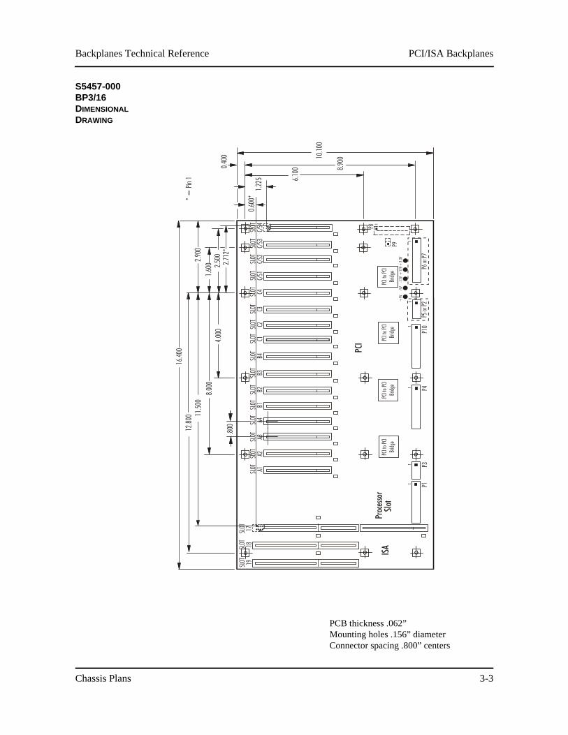
S5457-000 BP3/16 DIMENSIONAL DRAWING
PCB thickness .062”Mounting holes .156” diameterConnector spacing .800” centers

PCI/ISA Backplanes Backplanes Technical Reference
Chassis Plans3-4
S5457-000 BP3/16 CONNECTORS
______________________________________________________________________
NOTE: Pin 1 on the connectors is indicated by the square pad on the PCB.______________________________________________________________________
P1 - Power Supply Connector12 pin right angle, Molex #26-60-5120
Pin123456789101112
SignalNC+5V+12V-12VGndGndGndGnd-5V+5V+5V+5V
P2 - +5V Extended-Current Connector (optional)5 pin right angle, Amp #193839-431 Amps per circuit(Refer to Amp Doc. #108-1594)
Pin12345
Signal+5V+5V+5V+5V+5V
P3 - Auxiliary Power Supply Connector6 pin right angle, Molex #26-60-5060
Pin123456
Signal+5V+5V+5VGndGndGnd

PCI/ISA BackplanesBackplanes Technical Reference
Chassis Plans 3-5
S5457-000 BP3/16 CONNECTORS (CONTINUED)
P4 - Alternate Power Supply Connector10 position terminal block, Augat #2MV-1020 Amps per circuit
Pin12345678910
Signal+5V+5V+5VGndGndGndGnd-5V-12V+12V
P5 - Auxiliary Power Supply Connector6 pin right angle, Molex #26-60-5060
Pin123456
Signal+5V+5V+5VGndGndGnd
P6 - Power Supply Connector12 pin right angle, Molex #26-60-5120
Pin123456789101112
SignalNC+5V+12V-12VGndGndGndGnd-5V+5V+5V+5V
PCI/ISA Backplanes Backplanes Technical Reference
Chassis Plans3-6
S5457-000 BP3/16 CONNECTORS (CONTINUED)
P7 - +5V Return Extended-Current Connector (optional)5 pin right angle, Amp #193839-431 Amps per circuit(Refer to Amp Doc. #108-1594)
Pin12345
SignalGndGndGndGndGnd
P8 - ATX Connector (optional)20 pin dual row header, Molex #39-29-9202
Pin12345678910
Signal+3.3V+3.3VGnd+5VGnd+5VGndPW-OK+5VSB+12V
Pin11121314151617181920
Signal+3.3V-12VGndPS-ONGndGndGnd-5V+5V+5V
P9 - ATX Power-On Connector (optional)2 pin header, Amp #640456-2
Pin12
SignalPS-ONGnd
P10 - +3.3V Power Supply Connector12 pin right angle, Molex #26-60-5120
Pin123456789101112
Signal+3.3V+3.3V+3.3VGndGndGndGndGndGnd+3.3V+3.3V+3.3V

PCI/ISA BackplanesBackplanes Technical Reference
Chassis Plans 3-7
S5491-000 BP7/6
The BP7/6 is a PICMG-compatible backplane. It is a six-layer .062" thick PCB which provides seven ISA slots and six PCI Local Bus slots for use by standard PCI Local Bus option cards.
One of the seven ISA slots is dedicated to the SBC with PCI extension. The PCI slots support the PCI Local Bus 2.1 Specification. Two PCI slots are on the primary PCI Bus and four slots are on the secondary PCI Bus. The secondary PCI Bus is implemented using an Intel PCI-to-PCI bridge.
The standard AT power connection is available through a 12-pin AT-style connector. Power connection for +3.3V is available through a 12-pin AT-style connector or an ATX connector (optional).
PCI/ISA Backplanes Backplanes Technical Reference
Chassis Plans3-8
S5491-000 BP7/6 BUS DIAGRAM
_______________________________________________________________________
KEYBOARD DIAGRAM
PCI/ISA BackplanesBackplanes Technical Reference
Chassis Plans 3-9
S5491-000 BP7/6 DIMENSIONAL DRAWING
PCB thickness .062”Mounting holes .156” diameterConnector spacing .800” centers

PCI/ISA Backplanes Backplanes Technical Reference
Chassis Plans3-10
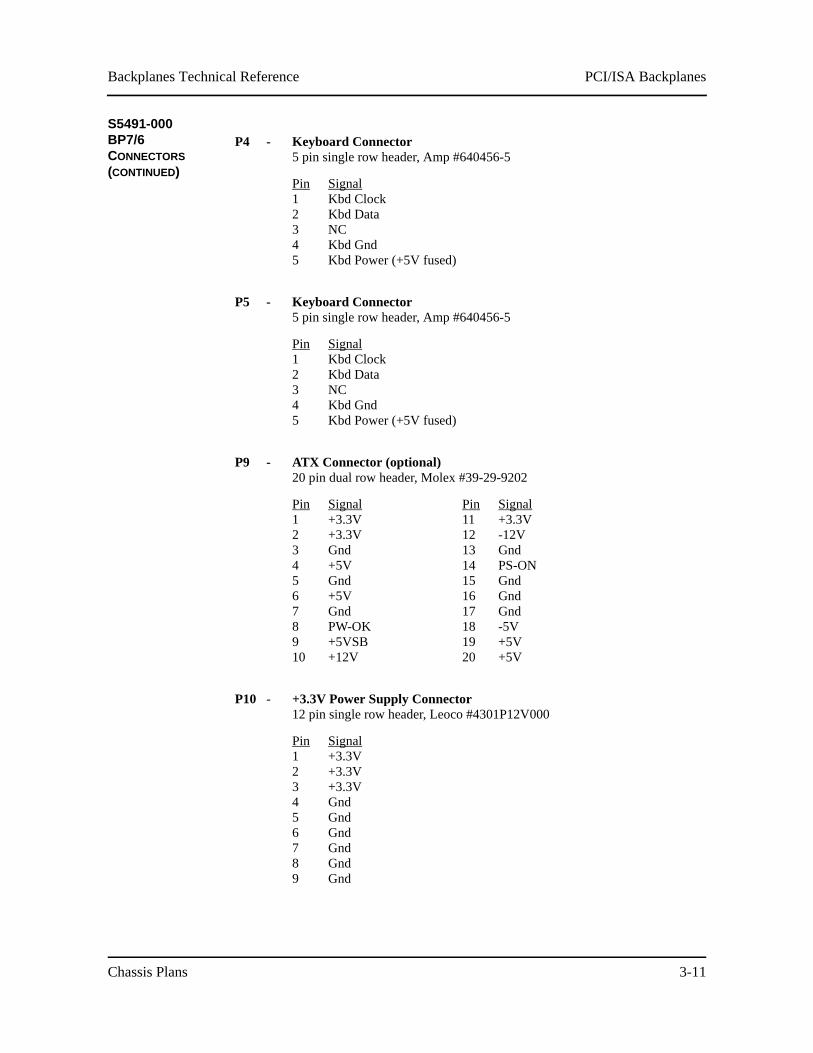
S5491-000 BP7/6 CONNECTORS
______________________________________________________________________
NOTE: Pin 1 on the connectors is indicated by the square pad on the PCB.______________________________________________________________________
P1 - Power Supply Connector12 pin single row header, Leoco #4301P12V000
Pin123456789101112
SignalNC+5V+12V-12VGndGndGndGnd-5V+5V+5V+5V
P2 - Auxiliary Power Supply Connector6 pin single row header, Burndy #GTC6R-1
Pin123456
Signal+5V+5V+5VGndGndGnd
P3 - Keyboard Connector5 pin DIN, Amp #520842-1
Pin12345
SignalKbd ClockKbd DataNCKbd GndKbd Power (+5V fused)
PCI/ISA BackplanesBackplanes Technical Reference
Chassis Plans 3-11
S5491-000 BP7/6 CONNECTORS (CONTINUED)
P4 - Keyboard Connector5 pin single row header, Amp #640456-5
Pin12345
SignalKbd ClockKbd DataNCKbd GndKbd Power (+5V fused)
P5 - Keyboard Connector5 pin single row header, Amp #640456-5
Pin12345
SignalKbd ClockKbd DataNCKbd GndKbd Power (+5V fused)
P9 - ATX Connector (optional)20 pin dual row header, Molex #39-29-9202
Pin12345678910
Signal+3.3V+3.3VGnd+5VGnd+5VGndPW-OK+5VSB+12V
Pin11121314151617181920
Signal+3.3V-12VGndPS-ONGndGndGnd-5V+5V+5V
P10 - +3.3V Power Supply Connector12 pin single row header, Leoco #4301P12V000
Pin123456789
Signal+3.3V+3.3V+3.3VGndGndGndGndGndGnd

PCI/ISA Backplanes Backplanes Technical Reference
Chassis Plans3-12
S5491-000 BP7/6 CONNECTORS (CONTINUED)
P10 - +3.3V Power Supply Connector (continued)
Pin101112
Signal+3.3V+3.3V+3.3V
P12 - ATX Power-On Connector (optional)2 pin header, Amp #640456-2
Pin12
SignalPS-ONGnd
PCI/ISA BackplanesBackplanes Technical Reference
Chassis Plans 3-13
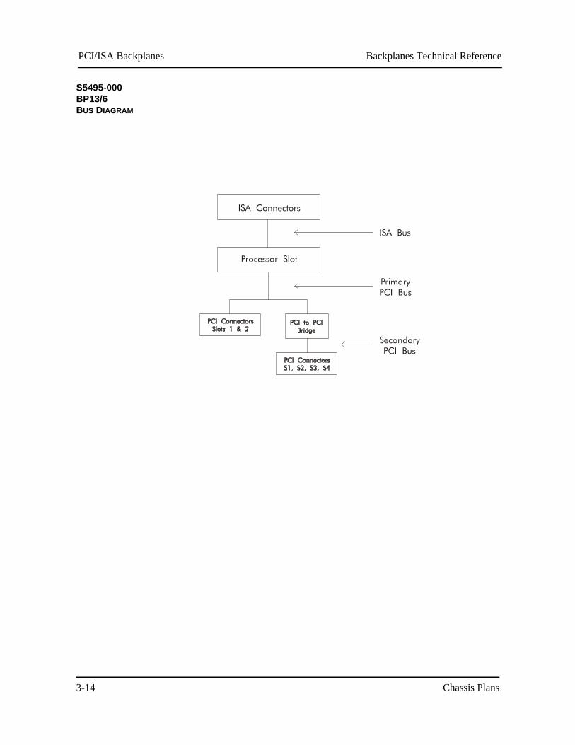
S5495-000 BP13/6
The BP13/6 is a PICMG-compatible backplane. It is a six-layer .062" thick PCB which provides 13 ISA slots and six PCI Local Bus slots for use by standard PCI Local Bus option cards.
One of the 13 ISA slots is dedicated to the SBC with PCI extension. The PCI slots support the PCI Local Bus 2.1 Specification. Two PCI slots are on the primary PCI Bus and four slots are on the secondary PCI Bus. The secondary PCI Bus is implemented using an Intel PCI-to-PCI bridge.
The standard AT power connection is available through two 12-pin .156 MTA connectors or one terminal block connector. Power connection for +3.3V is available through a 12-pin AT-style connector or an ATX connector (optional).
PCI/ISA Backplanes Backplanes Technical Reference
Chassis Plans3-14
S5495-000 BP13/6 BUS DIAGRAM
PCI/ISA BackplanesBackplanes Technical Reference
Chassis Plans 3-15
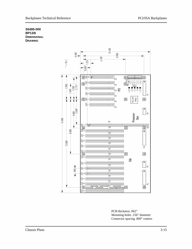
S5495-000 BP13/6 DIMENSIONAL DRAWING
PCB thickness .062”Mounting holes .156” diameterConnector spacing .800” centers

PCI/ISA Backplanes Backplanes Technical Reference
Chassis Plans3-16
S5495-000 BP13/6 CONNECTORS
______________________________________________________________________
NOTE: Pin 1 on the connectors is indicated by the square pad on the PCB.______________________________________________________________________
P1 - Power Supply Connector12 pin right angle, Molex #26-60-5120
Pin123456789101112
SignalNC+5V+12V-12VGndGndGndGnd-5V+5V+5V+5V
P3 - Auxiliary Power Supply Connector6 pin right angle, Molex #26-60-5060
Pin123456
Signal+5V+5V+5VGndGndGnd
P4 - Alternate Power Supply Connector10 position terminal block, Augat #2MV-10
Pin12345678910
Signal+5V+5V+5VGndGndGndGnd-5V-12V+12V
PCI/ISA BackplanesBackplanes Technical Reference
Chassis Plans 3-17
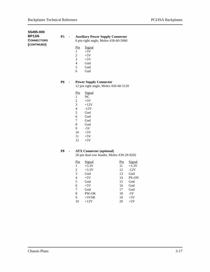
S5495-000 BP13/6 CONNECTORS (CONTINUED)
P5 - Auxiliary Power Supply Connector6 pin right angle, Molex #26-60-5060
Pin123456
Signal+5V+5V+5VGndGndGnd
P6 - Power Supply Connector12 pin right angle, Molex #26-60-5120
Pin123456789101112
SignalNC+5V+12V-12VGndGndGndGnd-5V+5V+5V+5V
P8 - ATX Connector (optional)20 pin dual row header, Molex #39-29-9202
Pin12345678910
Signal+3.3V+3.3VGnd+5VGnd+5VGndPW-OK+5VSB+12V
Pin11121314151617181920
Signal+3.3V-12VGndPS-ONGndGndGnd-5V+5V+5V
PCI/ISA Backplanes Backplanes Technical Reference
Chassis Plans3-18
S5495-000 BP13/6 CONNECTORS (CONTINUED)
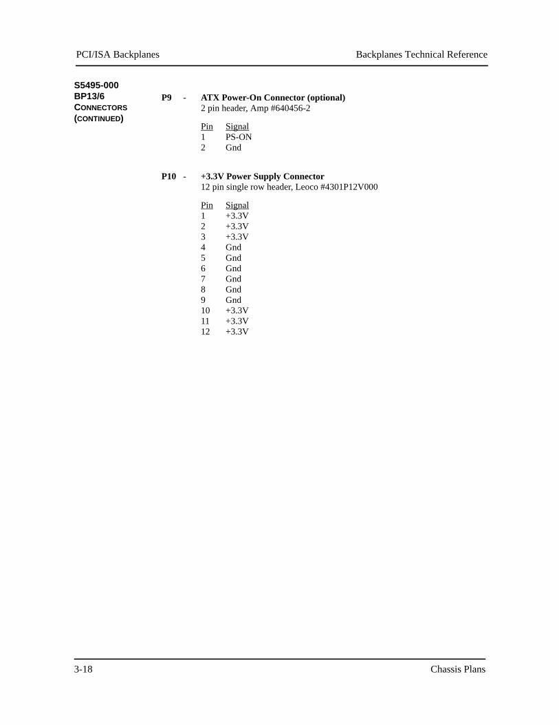
P9 - ATX Power-On Connector (optional)2 pin header, Amp #640456-2
Pin12
SignalPS-ONGnd
P10 - +3.3V Power Supply Connector12 pin single row header, Leoco #4301P12V000
Pin123456789101112
Signal+3.3V+3.3V+3.3VGndGndGndGndGndGnd+3.3V+3.3V+3.3V
PCI/ISA BackplanesBackplanes Technical Reference
Chassis Plans 3-19
S5498-000 BP17/3
The BP17/3 is a PICMG-compatible backplane. It is a six-layer .062" thick PCB which provides 17 ISA slots and three PCI Local Bus slots for use by standard PCI Local Bus option cards.
One of the 17 ISA slots is dedicated to the SBC with PCI extension. The PCI slots support the PCI Local Bus 2.1 Specification.
The standard AT power connection is available through two 12-pin .156 MTA connectors or one terminal block connector. Power connection for +3.3V is available through a 12-pin .156 MTA connector or an ATX connector (optional).
PCI/ISA Backplanes Backplanes Technical Reference
Chassis Plans3-20
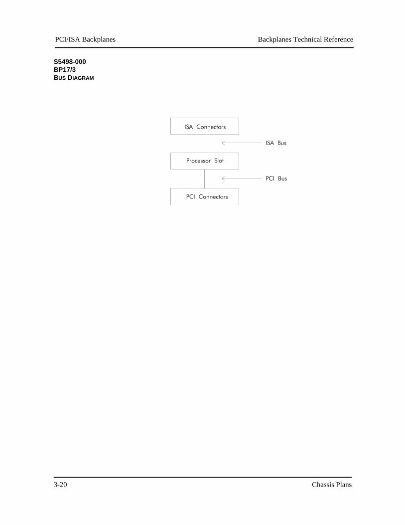
S5498-000 BP17/3 BUS DIAGRAM
PCI/ISA BackplanesBackplanes Technical Reference
Chassis Plans 3-21
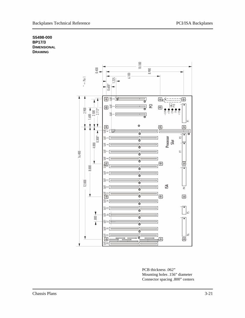
S5498-000 BP17/3 DIMENSIONAL DRAWING
PCB thickness .062”Mounting holes .156” diameterConnector spacing .800” centers
PCI/ISA Backplanes Backplanes Technical Reference
Chassis Plans3-22
S5498-000 BP17/3 CONNECTORS
______________________________________________________________________
NOTE: Pin 1 on the connectors is indicated by the square pad on the PCB.______________________________________________________________________
P1 - Power Supply Connector12 pin right angle, Molex #26-60-5120
Pin123456789101112
SignalNC+5V+12V-12VGndGndGndGnd-5V+5V+5V+5V
P3 - Auxiliary Power Supply Connector6 pin right angle, Molex #26-60-5060
Pin123456
Signal+5V+5V+5VGndGndGnd
P4 - Alternate Power Supply Connector10 position terminal block, Augat #2MV-10
Pin12345678910
Signal+5V+5V+5VGndGndGndGnd-5V-12V+12V
PCI/ISA BackplanesBackplanes Technical Reference
Chassis Plans 3-23
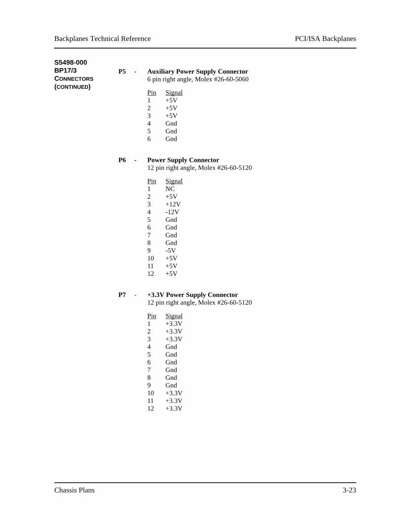
S5498-000 BP17/3 CONNECTORS (CONTINUED)
P5 - Auxiliary Power Supply Connector6 pin right angle, Molex #26-60-5060
Pin123456
Signal+5V+5V+5VGndGndGnd
P6 - Power Supply Connector12 pin right angle, Molex #26-60-5120
Pin123456789101112
SignalNC+5V+12V-12VGndGndGndGnd-5V+5V+5V+5V
P7 - +3.3V Power Supply Connector12 pin right angle, Molex #26-60-5120
Pin123456789101112
Signal+3.3V+3.3V+3.3VGndGndGndGndGndGnd+3.3V+3.3V+3.3V

PCI/ISA Backplanes Backplanes Technical Reference
Chassis Plans3-24
S5498-000 BP17/3 CONNECTORS (CONTINUED)
P9 - ATX Connector (optional)20 pin dual row header, Molex #39-29-9202
Pin12345678910
Signal+3.3V+3.3VGnd+5VGnd+5VGndPW-OK+5VSB+12V
Pin11121314151617181920
Signal+3.3V-12VGndPS-ONGndGndGnd-5V+5V+5V
P10 - ATX Power-On Connector (optional)2 pin header, Amp #640456-2
Pin12
SignalPS-ONGnd
PCI/ISA BackplanesBackplanes Technical Reference
Chassis Plans 3-25
S5501-000 BP11/3
The BP11/3 is a PICMG-compatible backplane. It is a six-layer .062" thick PCB which provides 11 ISA slots and three PCI Local Bus slots for use by standard PCI Local Bus option cards.
One of the 11 ISA slots is dedicated to the SBC with PCI extension. The PCI slots support the PCI Local Bus 2.1 Specification.
The standard AT power connection is available through a 12-pin AT-style connector. Power connection for +3.3V is available through a 12-pin AT-style connector or an ATX connector (optional).
PCI/ISA Backplanes Backplanes Technical Reference
Chassis Plans3-26
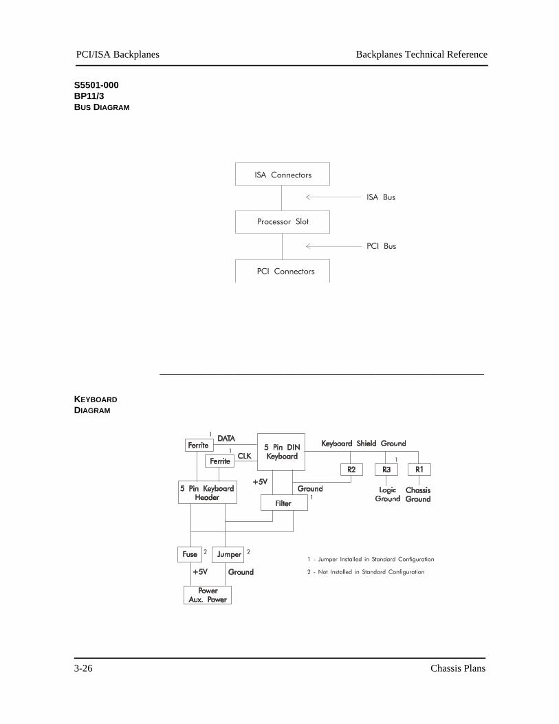
S5501-000 BP11/3 BUS DIAGRAM
_______________________________________________________________________
KEYBOARD DIAGRAM
PCI/ISA BackplanesBackplanes Technical Reference
Chassis Plans 3-27
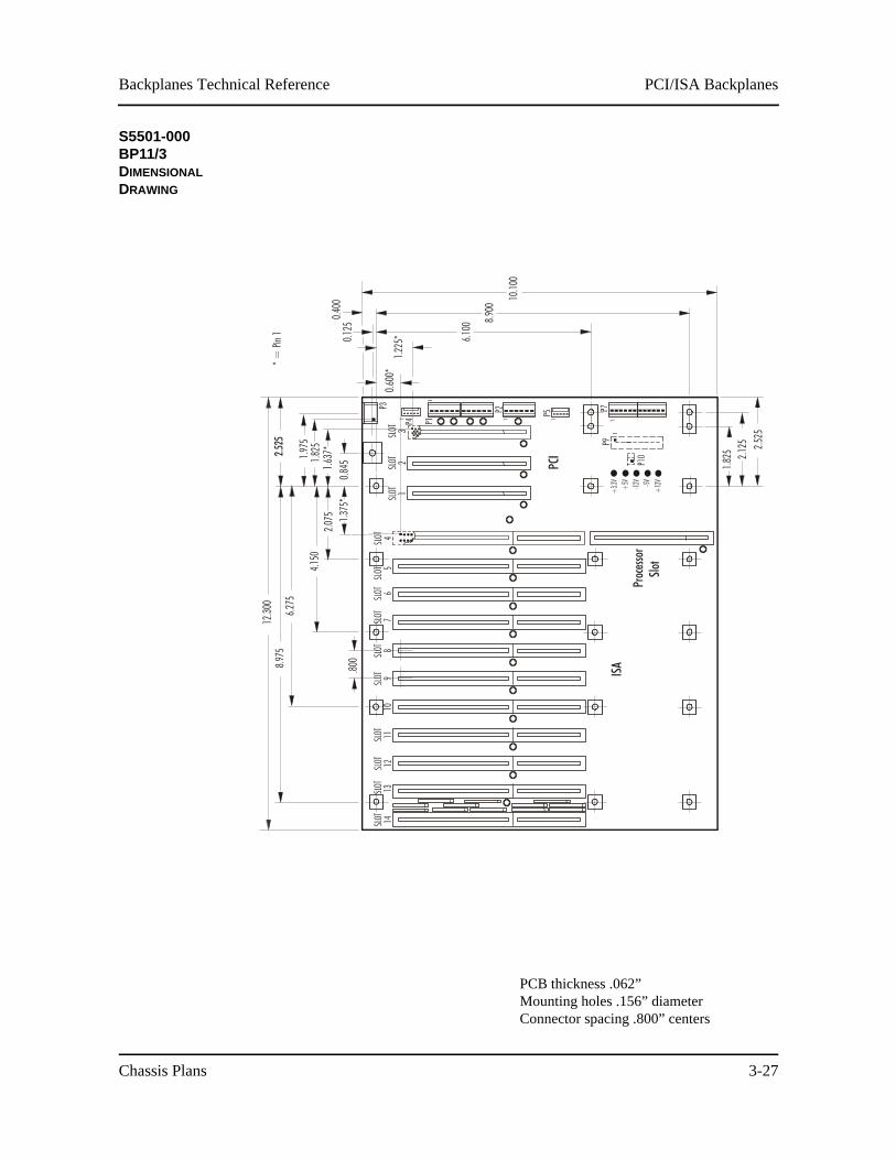
S5501-000 BP11/3 DIMENSIONAL DRAWING
PCB thickness .062”Mounting holes .156” diameterConnector spacing .800” centers
PCI/ISA Backplanes Backplanes Technical Reference
Chassis Plans3-28
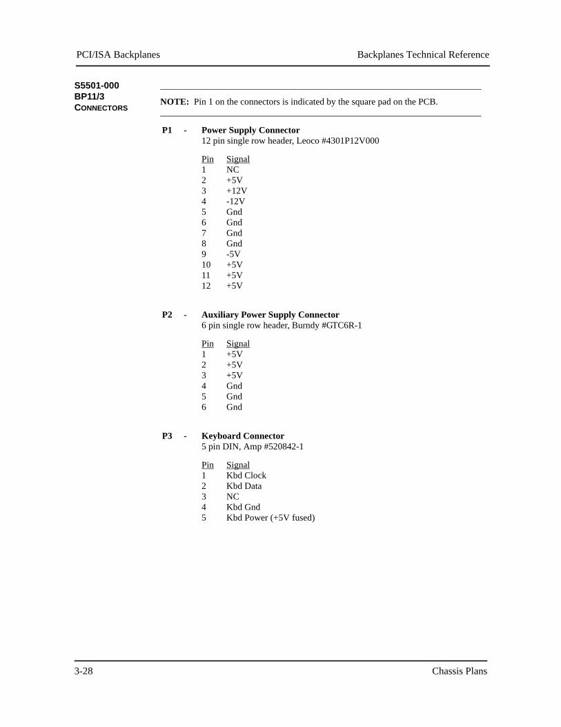
S5501-000 BP11/3 CONNECTORS
______________________________________________________________________
NOTE: Pin 1 on the connectors is indicated by the square pad on the PCB.______________________________________________________________________
P1 - Power Supply Connector12 pin single row header, Leoco #4301P12V000
Pin123456789101112
SignalNC+5V+12V-12VGndGndGndGnd-5V+5V+5V+5V
P2 - Auxiliary Power Supply Connector6 pin single row header, Burndy #GTC6R-1
Pin123456
Signal+5V+5V+5VGndGndGnd
P3 - Keyboard Connector5 pin DIN, Amp #520842-1
Pin12345
SignalKbd ClockKbd DataNCKbd GndKbd Power (+5V fused)
PCI/ISA BackplanesBackplanes Technical Reference
Chassis Plans 3-29
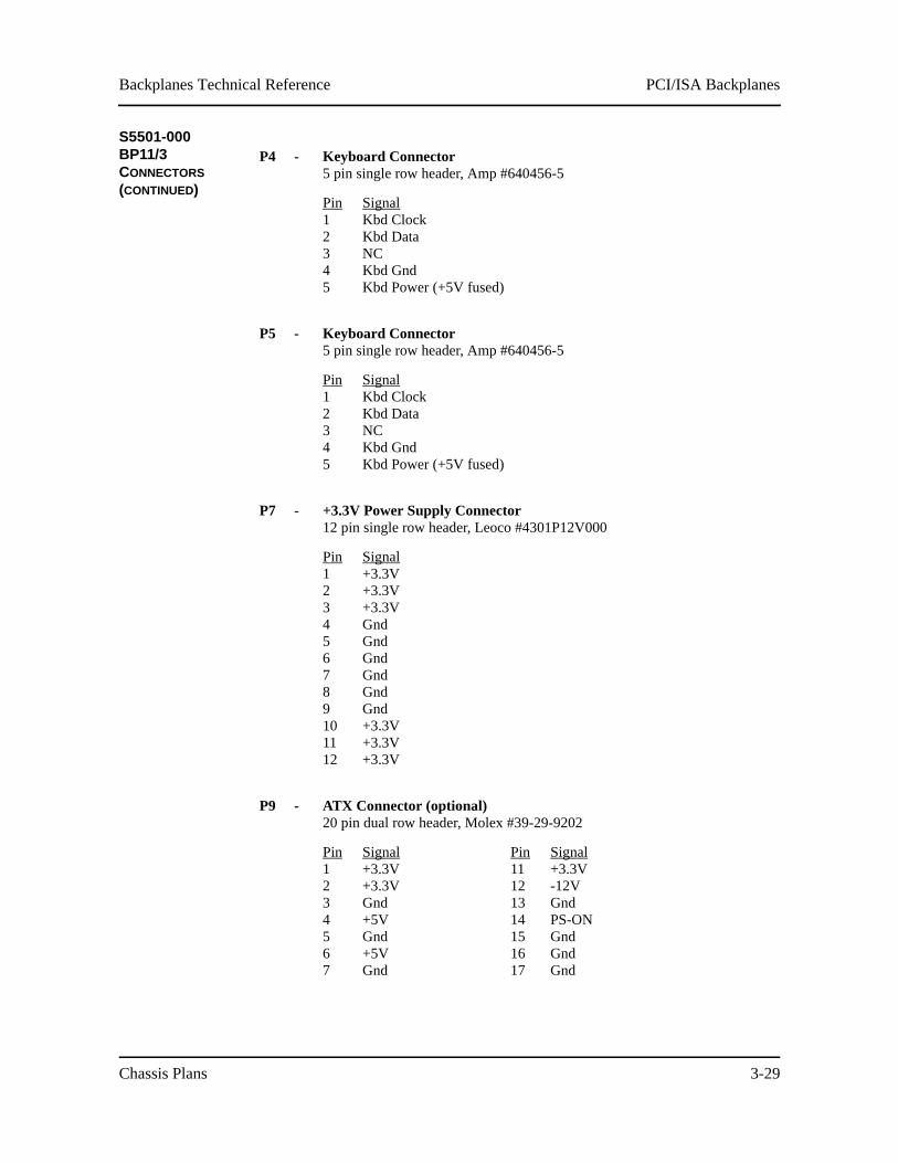
S5501-000 BP11/3 CONNECTORS (CONTINUED)
P4 - Keyboard Connector5 pin single row header, Amp #640456-5
Pin12345
SignalKbd ClockKbd DataNCKbd GndKbd Power (+5V fused)
P5 - Keyboard Connector5 pin single row header, Amp #640456-5
Pin12345
SignalKbd ClockKbd DataNCKbd GndKbd Power (+5V fused)
P7 - +3.3V Power Supply Connector12 pin single row header, Leoco #4301P12V000
Pin123456789101112
Signal+3.3V+3.3V+3.3VGndGndGndGndGndGnd+3.3V+3.3V+3.3V
P9 - ATX Connector (optional)20 pin dual row header, Molex #39-29-9202
Pin1234567
Signal+3.3V+3.3VGnd+5VGnd+5VGnd
Pin11121314151617
Signal+3.3V-12VGndPS-ONGndGndGnd
PCI/ISA Backplanes Backplanes Technical Reference
Chassis Plans3-30
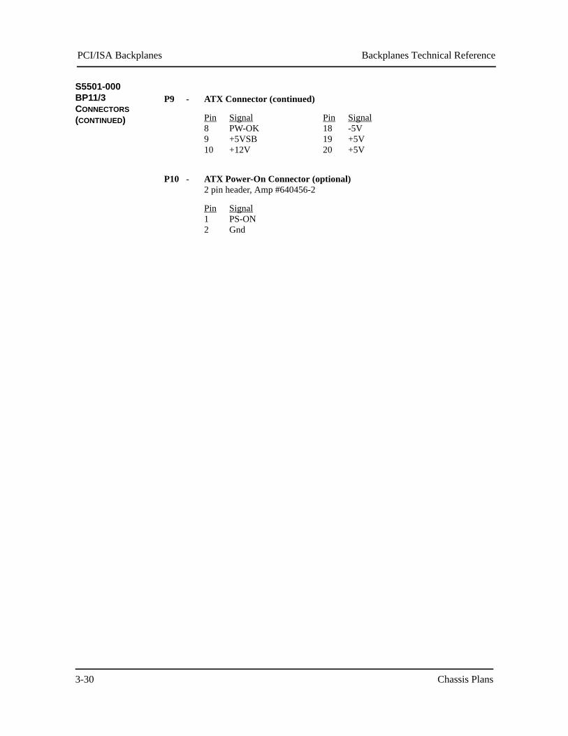
S5501-000 BP11/3 CONNECTORS (CONTINUED)
P9 - ATX Connector (continued)
Pin8910
SignalPW-OK+5VSB+12V
Pin181920
Signal-5V+5V+5V
P10 - ATX Power-On Connector (optional)2 pin header, Amp #640456-2
Pin12
SignalPS-ONGnd
PCI/ISA BackplanesBackplanes Technical Reference
Chassis Plans 3-31
S5504-000 BP5/3
The BP5/3 is a PICMG-compatible backplane. It is a six-layer .062" thick PCB which provides five ISA slots and three PCI Local Bus slots for use by standard PCI Local Bus option cards.
One of the five ISA slots is dedicated to the SBC with PCI extension. The PCI slots support the PCI Local Bus 2.1 Specification.
The standard AT power connection is available through a 12-pin AT-style connector. Power connection for +3.3V is available through a 12-pin AT-style connector or an ATX connector (optional).

PCI/ISA Backplanes Backplanes Technical Reference
Chassis Plans3-32
S5504-000 BP5/3 BUS DIAGRAM
_______________________________________________________________________
KEYBOARD DIAGRAM
PCI/ISA BackplanesBackplanes Technical Reference
Chassis Plans 3-33
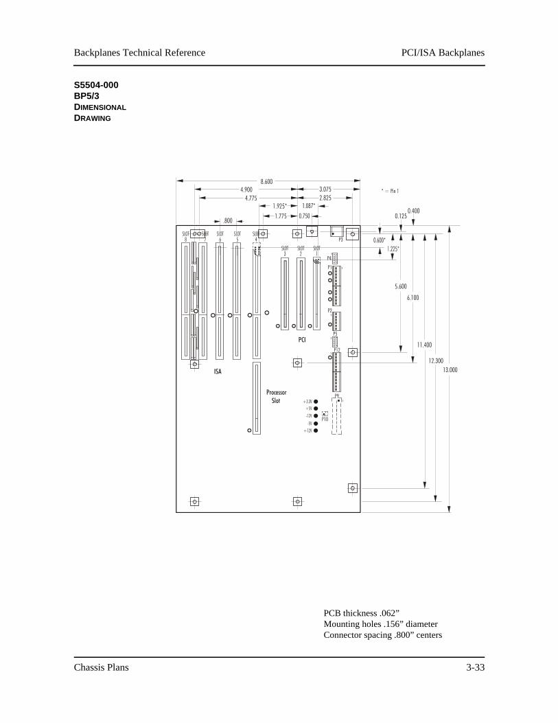
S5504-000 BP5/3 DIMENSIONAL DRAWING
PCB thickness .062”Mounting holes .156” diameterConnector spacing .800” centers
PCI/ISA Backplanes Backplanes Technical Reference
Chassis Plans3-34
S5504-000 BP5/3 CONNECTORS
______________________________________________________________________
NOTE: Pin 1 on the connectors is indicated by the square pad on the PCB.______________________________________________________________________
P1 - Power Supply Connector12 pin single row header, Leoco #4301P12V000
Pin123456789101112
SignalNC+5V+12V-12VGndGndGndGnd-5V+5V+5V+5V
P2 - Auxiliary Power Supply Connector6 pin single row header, Burndy #GTC6R-1
Pin123456
Signal+5V+5V+5VGndGndGnd
P3 - Keyboard Connector5 pin DIN, Amp #520842-1
Pin12345
SignalKbd ClockKbd DataNCKbd GndKbd Power (+5V fused)
P4 - Keyboard Connector5 pin single row header, Amp #640456-5
Pin12345
SignalKbd ClockKbd DataNCKbd GndKbd Power (+5V fused)
PCI/ISA BackplanesBackplanes Technical Reference
Chassis Plans 3-35
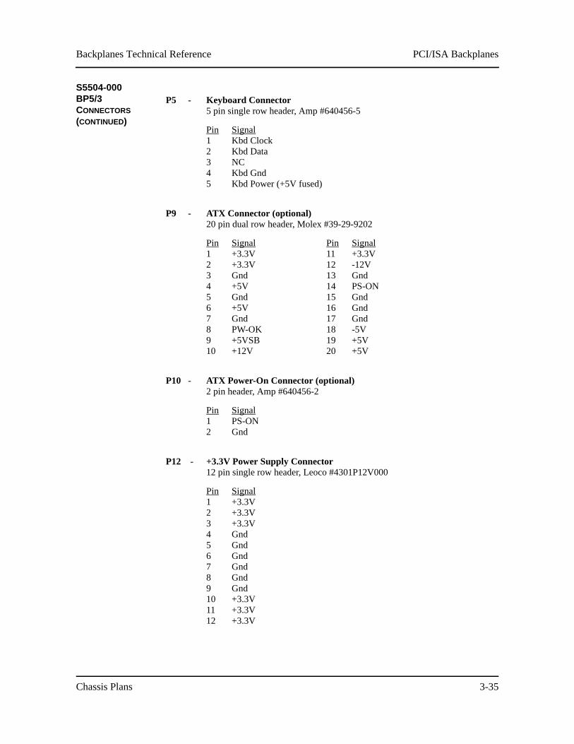
S5504-000 BP5/3 CONNECTORS (CONTINUED)
P5 - Keyboard Connector5 pin single row header, Amp #640456-5
Pin12345
SignalKbd ClockKbd DataNCKbd GndKbd Power (+5V fused)
P9 - ATX Connector (optional)20 pin dual row header, Molex #39-29-9202
Pin12345678910
Signal+3.3V+3.3VGnd+5VGnd+5VGndPW-OK+5VSB+12V
Pin11121314151617181920
Signal+3.3V-12VGndPS-ONGndGndGnd-5V+5V+5V
P10 - ATX Power-On Connector (optional)2 pin header, Amp #640456-2
Pin12
SignalPS-ONGnd
P12 - +3.3V Power Supply Connector12 pin single row header, Leoco #4301P12V000
Pin123456789101112
Signal+3.3V+3.3V+3.3VGndGndGndGndGndGnd+3.3V+3.3V+3.3V
PCI/ISA Backplanes Backplanes Technical Reference
Chassis Plans3-36
This page intentionally left blank.
PCI/ISA BackplanesBackplanes Technical Reference
Chassis Plans 3-37
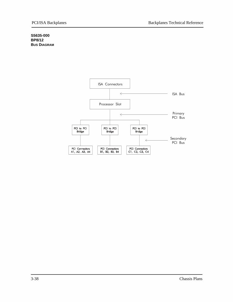
S5635-000 BP8/12
The BP8/12 is a PICMG-compatible backplane. It is a six-layer .062" thick PCB which provides eight ISA slots and 12 PCI Local Bus slots for use by standard PCI Local Bus option cards.
One of the eight ISA slots is dedicated to the SBC with PCI extension. The PCI slots support the PCI Local Bus 2.1 Specification. The 12 PCI slots are on the secondary PCI Bus, which is implemented using three Intel PCI-to-PCI bridges.
The standard AT power connection is available through two 12-pin .156 MTA connectors or one terminal block connector. Power connection for +3.3V is available through a 12-pin .156 MTA connector or an ATX connector (optional).
PCI/ISA Backplanes Backplanes Technical Reference
Chassis Plans3-38
S5635-000 BP8/12 BUS DIAGRAM
PCI/ISA BackplanesBackplanes Technical Reference
Chassis Plans 3-39
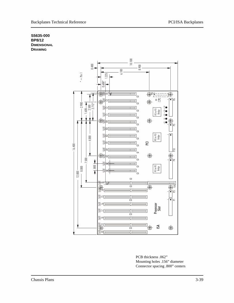
S5635-000 BP8/12 DIMENSIONAL DRAWING
PCB thickness .062”Mounting holes .156” diameterConnector spacing .800” centers

PCI/ISA Backplanes Backplanes Technical Reference
Chassis Plans3-40
S5635-000 BP8/12 CONNECTORS
______________________________________________________________________
NOTE: Pin 1 on the connectors is indicated by the square pad on the PCB.______________________________________________________________________
P1 - Power Supply Connector12 pin right angle, Molex #26-60-5120
Pin123456789101112
SignalNC+5V+12V-12VGndGndGndGnd-5V+5V+5V+5V
P3 - Auxiliary Power Supply Connector6 pin right angle, Molex #26-60-5060
Pin123456
Signal+5V+5V+5VGndGndGnd
P4 - Alternate Power Supply Connector12 position terminal block, Augat #2MV-12
Pin123456789101112
Signal+5V+5V+5V+5VGndGndGndGndGnd-5V-12V+12V
PCI/ISA BackplanesBackplanes Technical Reference
Chassis Plans 3-41
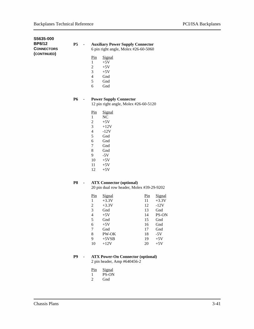
S5635-000 BP8/12 CONNECTORS (CONTINUED)
P5 - Auxiliary Power Supply Connector6 pin right angle, Molex #26-60-5060
Pin123456
Signal+5V+5V+5VGndGndGnd
P6 - Power Supply Connector12 pin right angle, Molex #26-60-5120
Pin123456789101112
SignalNC+5V+12V-12VGndGndGndGnd-5V+5V+5V+5V
P8 - ATX Connector (optional)20 pin dual row header, Molex #39-29-9202
Pin12345678910
Signal+3.3V+3.3VGnd+5VGnd+5VGndPW-OK+5VSB+12V
Pin11121314151617181920
Signal+3.3V-12VGndPS-ONGndGndGnd-5V+5V+5V
P9 - ATX Power-On Connector (optional)2 pin header, Amp #640456-2
Pin12
SignalPS-ONGnd
PCI/ISA Backplanes Backplanes Technical Reference
Chassis Plans3-42
S5635-000 BP8/12 CONNECTORS (CONTINUED)
P10 - +3.3V Power Supply Connector12 pin right angle, Molex #26-60-5120
Pin123456789101112
Signal+3.3V+3.3V+3.3VGndGndGndGndGndGnd+3.3V+3.3V+3.3V
PCI/ISA BackplanesBackplanes Technical Reference
Chassis Plans 3-43
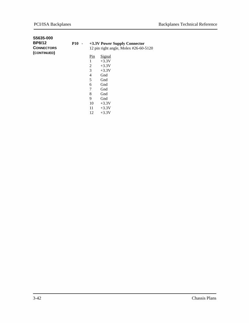
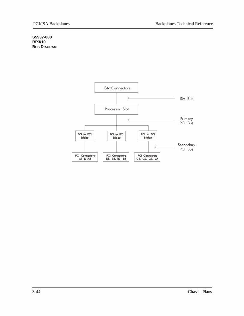
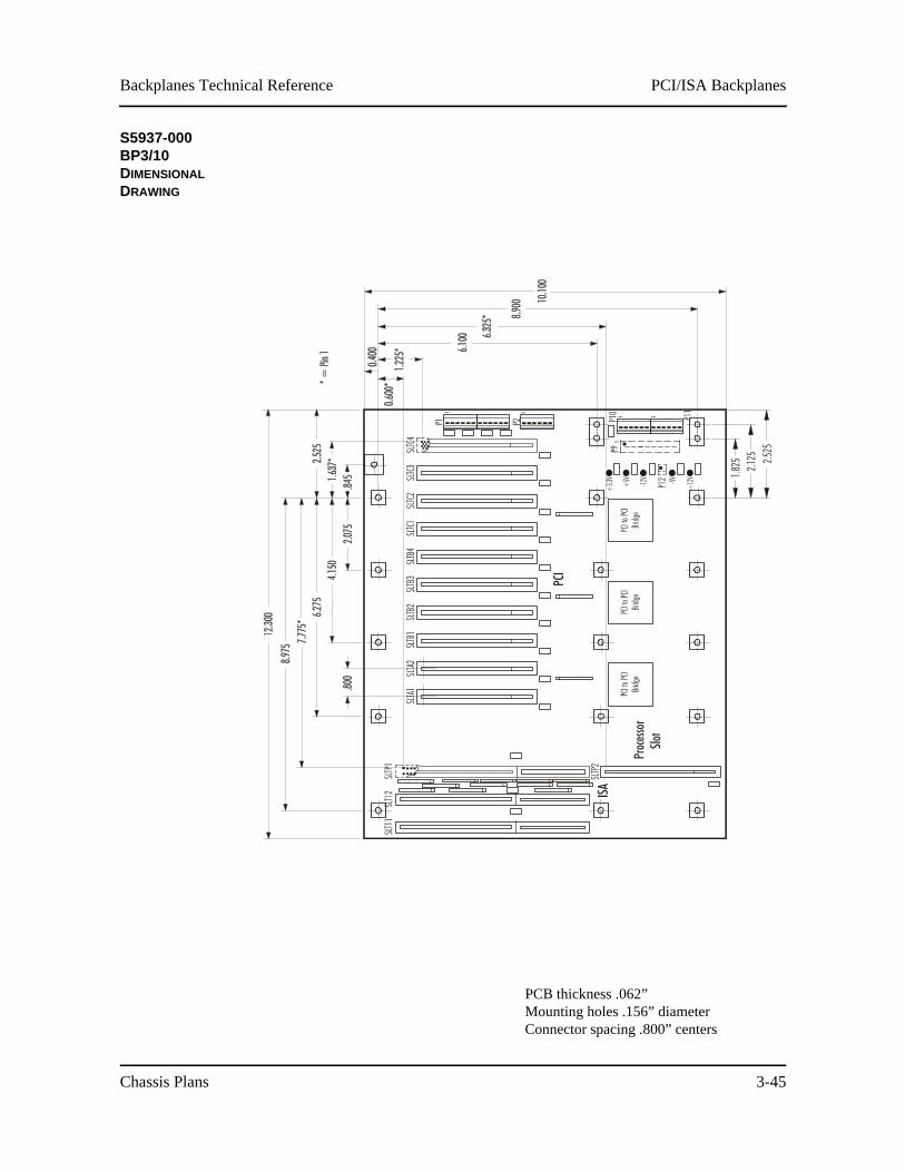
S5937-000 BP3/10
The BP3/10 is a PICMG-compatible backplane. It is a six-layer .062" thick PCB which provides three ISA slots and ten 32-bit/33MHz PCI Local Bus slots for use by standard PCI Local Bus option cards.
One of the three ISA slots is dedicated to the SBC with PCI extension. The PCI slots support the PCI Local Bus 2.1 Specification. The ten PCI slots are on the secondary PCI Bus, which is implemented using three Intel PCI-to-PCI bridges.
The standard AT power connection is available through a 12-pin AT-style connector. Power connection for +3.3V is available through two 6-pin AT-style connectors or an ATX connector (optional).
PCI/ISA Backplanes Backplanes Technical Reference
Chassis Plans3-44
S5937-000 BP3/10 BUS DIAGRAM
PCI/ISA BackplanesBackplanes Technical Reference
Chassis Plans 3-45
S5937-000 BP3/10 DIMENSIONAL DRAWING
PCB thickness .062”Mounting holes .156” diameterConnector spacing .800” centers

PCI/ISA Backplanes Backplanes Technical Reference
Chassis Plans3-46
S5937-000 BP3/10 CONNECTORS
______________________________________________________________________
NOTE: Pin 1 on the connectors is indicated by the square pad on the PCB.______________________________________________________________________
P1 - Power Supply Connector12 pin single row header, Leoco #4301P12V000
Pin123456789101112
SignalNC+5V+12V-12VGndGndGndGnd-5V+5V+5V+5V
P2 - Auxiliary Power Supply Connector6 pin single row header, Burndy #GTC6R-1
Pin123456
Signal+5V+5V+5VGndGndGnd
P9 - ATX Connector (optional)20 pin dual row header, Molex #39-29-9202
Pin12345678910
Signal+3.3V+3.3VGnd+5VGnd+5VGndPW-OK+5VSB+12V
Pin11121314151617181920
Signal+3.3V-12VGndPS-ONGndGndGnd-5V+5V+5V
PCI/ISA BackplanesBackplanes Technical Reference
Chassis Plans 3-47
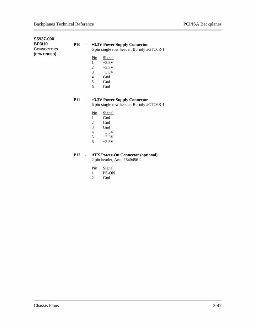
S5937-000 BP3/10 CONNECTORS (CONTINUED)
P10 - +3.3V Power Supply Connector6 pin single row header, Burndy #GTC6R-1
Pin123456
Signal+3.3V+3.3V+3.3VGndGndGnd
P11 - +3.3V Power Supply Connector6 pin single row header, Burndy #GTC6R-1
Pin123456
SignalGndGndGnd+3.3V+3.3V+3.3V
P12 - ATX Power-On Connector (optional)2 pin header, Amp #640456-2
Pin12
SignalPS-ONGnd

PCI/ISA Backplanes Backplanes Technical Reference
Chassis Plans3-48
This page intentionally left blank.
Copyright 2006 by Trenton Technology Inc. All rights reserved.
64-Bit BackplanesBackplanes Technical Reference
Chassis Plans 4-1
Chapter 4 64-Bit Backplanes
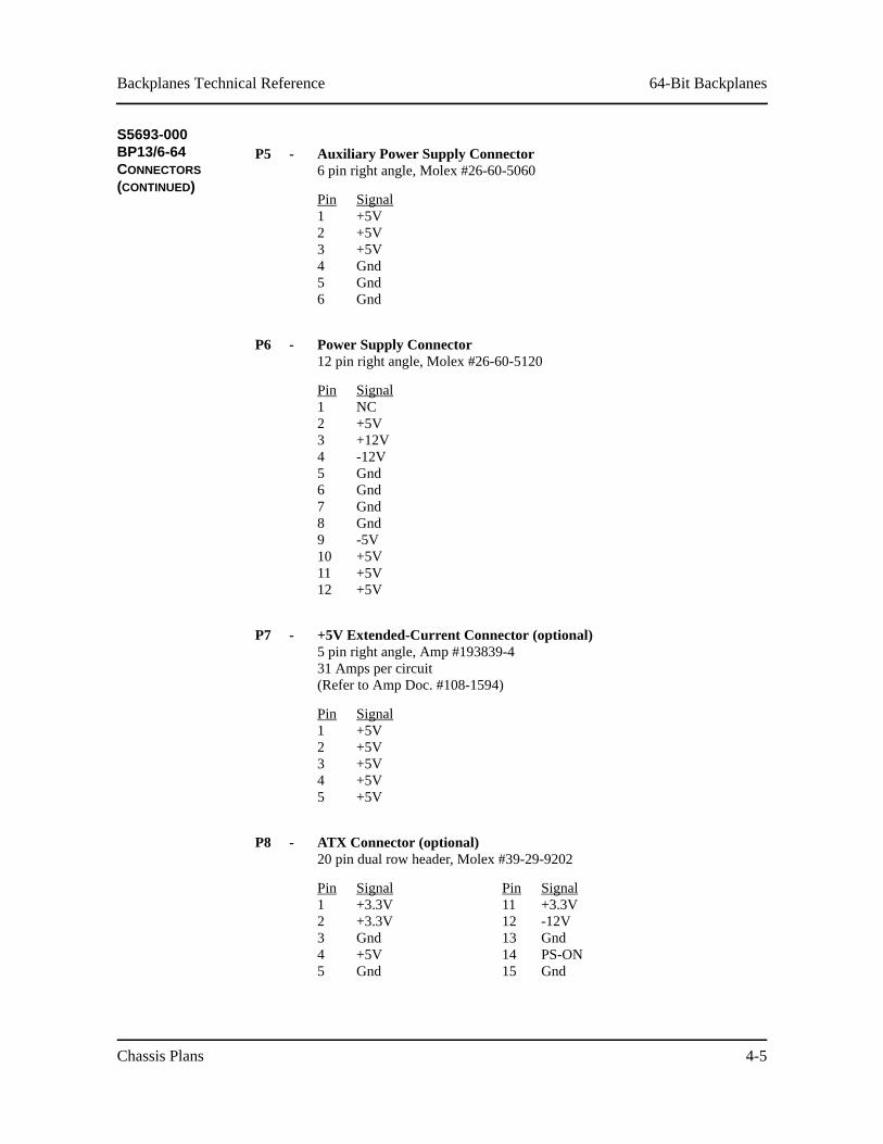
S5693-000 BP13/6-64
The BP13/6-64 is a PICMG-compatible backplane. It is a six-layer .062" thick PCB which provides 12 ISA slots, a 64-bit SBC slot and six 64-bit PCI option slots for use by standard PCI Local Bus option cards.
Either 64-bit or 32-bit SBCs and option cards may be used. 64-bit option cards can take advantage of the 64-bit architecture when communicating with each other, even if a 32-bit SBC is used.
The PCI slots support the PCI Local Bus 2.1 Specification. Two of the PCI slots are on the primary PCI Bus and the remaining four PCI slots are on the secondary PCI Bus, which is implemented using an Intel PCI-to-PCI bridge.
The standard AT power connection is available through two 12-pin .156 MTA connectors or one terminal block connector. Power connection for +3.3V is available through a 12-pin .156 MTA connector or an ATX connector (optional).
An extended-current option is also available. The extended-current connectors provide additional power capacity up to 150 Amps of +5V for power-intensive applications.

64-Bit Backplanes Backplanes Technical Reference
Chassis Plans4-2
S5693-000 BP13/6-64 BUS DIAGRAM
64-Bit BackplanesBackplanes Technical Reference
Chassis Plans 4-3
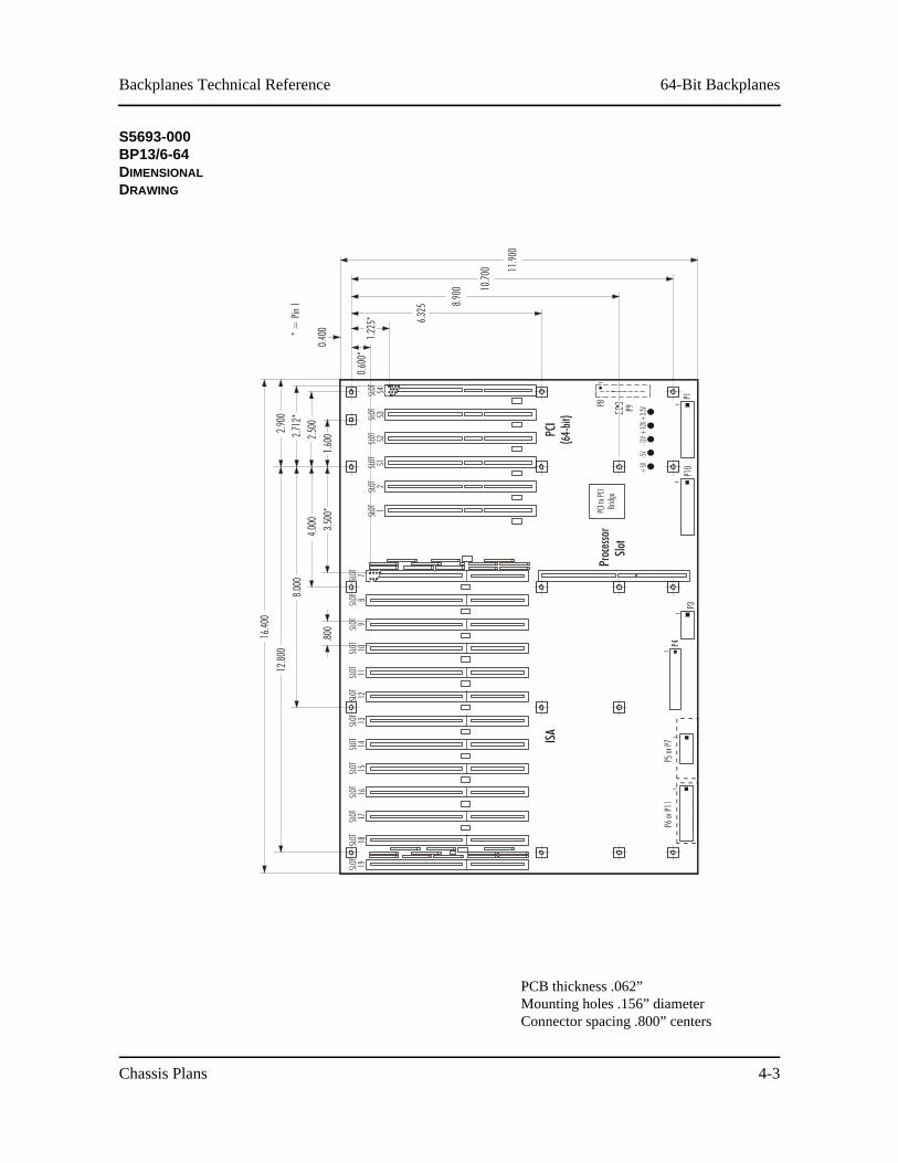
S5693-000 BP13/6-64 DIMENSIONAL DRAWING
PCB thickness .062”Mounting holes .156” diameterConnector spacing .800” centers
64-Bit Backplanes Backplanes Technical Reference
Chassis Plans4-4
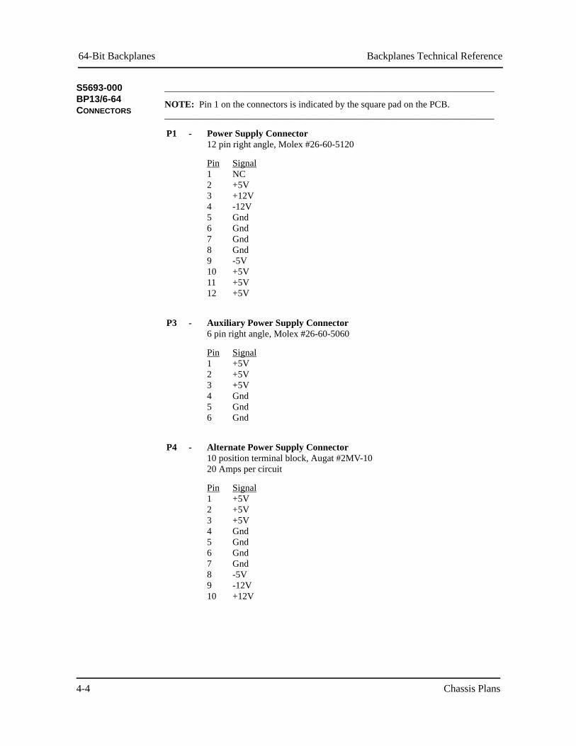
S5693-000 BP13/6-64 CONNECTORS
______________________________________________________________________
NOTE: Pin 1 on the connectors is indicated by the square pad on the PCB.______________________________________________________________________
P1 - Power Supply Connector12 pin right angle, Molex #26-60-5120
Pin123456789101112
SignalNC+5V+12V-12VGndGndGndGnd-5V+5V+5V+5V
P3 - Auxiliary Power Supply Connector6 pin right angle, Molex #26-60-5060
Pin123456
Signal+5V+5V+5VGndGndGnd
P4 - Alternate Power Supply Connector10 position terminal block, Augat #2MV-1020 Amps per circuit
Pin12345678910
Signal+5V+5V+5VGndGndGndGnd-5V-12V+12V
64-Bit BackplanesBackplanes Technical Reference
Chassis Plans 4-5
S5693-000 BP13/6-64 CONNECTORS (CONTINUED)
P5 - Auxiliary Power Supply Connector6 pin right angle, Molex #26-60-5060
Pin123456
Signal+5V+5V+5VGndGndGnd
P6 - Power Supply Connector12 pin right angle, Molex #26-60-5120
Pin123456789101112
SignalNC+5V+12V-12VGndGndGndGnd-5V+5V+5V+5V
P7 - +5V Extended-Current Connector (optional)5 pin right angle, Amp #193839-431 Amps per circuit(Refer to Amp Doc. #108-1594)
Pin12345
Signal+5V+5V+5V+5V+5V
P8 - ATX Connector (optional)20 pin dual row header, Molex #39-29-9202
Pin12345
Signal+3.3V+3.3VGnd+5VGnd
Pin1112131415
Signal+3.3V-12VGndPS-ONGnd
64-Bit Backplanes Backplanes Technical Reference
Chassis Plans4-6
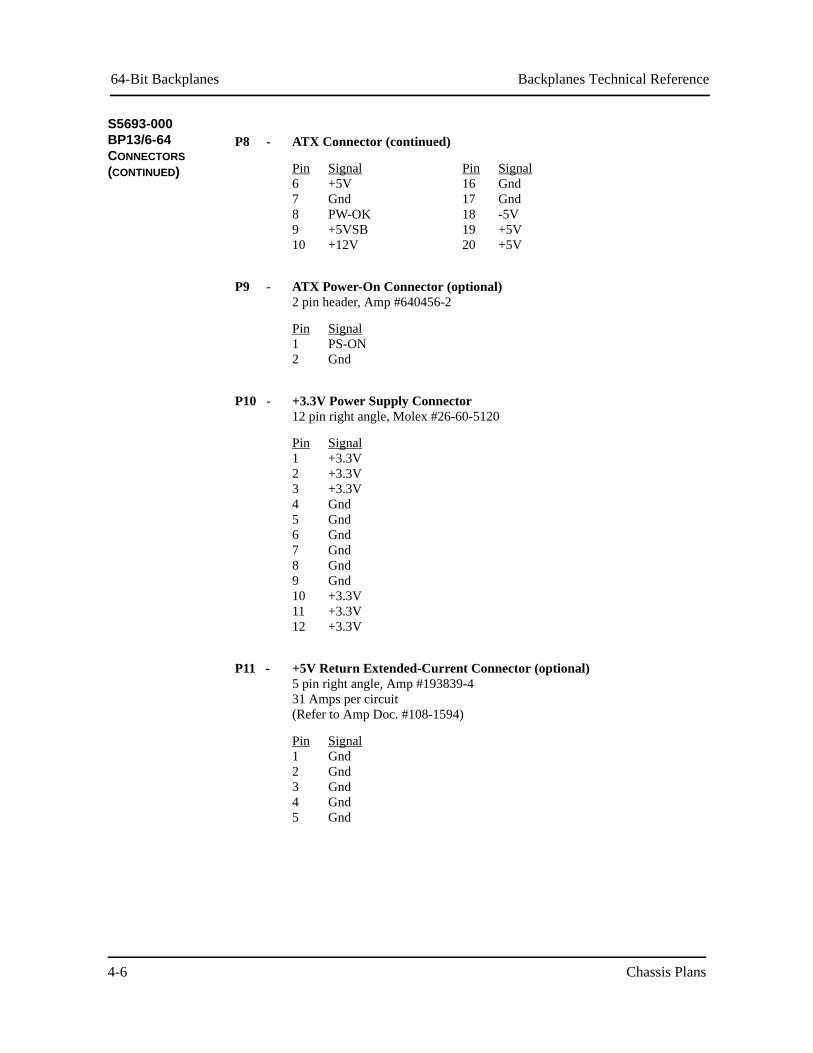
S5693-000 BP13/6-64 CONNECTORS (CONTINUED)
P8 - ATX Connector (continued)
Pin678910
Signal+5VGndPW-OK+5VSB+12V
Pin1617181920
SignalGndGnd-5V+5V+5V
P9 - ATX Power-On Connector (optional)2 pin header, Amp #640456-2
Pin12
SignalPS-ONGnd
P10 - +3.3V Power Supply Connector12 pin right angle, Molex #26-60-5120
Pin123456789101112
Signal+3.3V+3.3V+3.3VGndGndGndGndGndGnd+3.3V+3.3V+3.3V
P11 - +5V Return Extended-Current Connector (optional)5 pin right angle, Amp #193839-431 Amps per circuit(Refer to Amp Doc. #108-1594)
Pin12345
SignalGndGndGndGndGnd
64-Bit BackplanesBackplanes Technical Reference
Chassis Plans 4-7
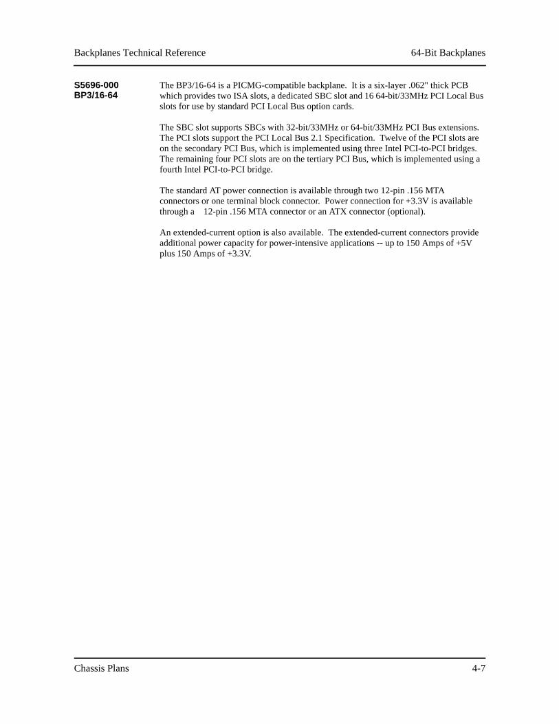
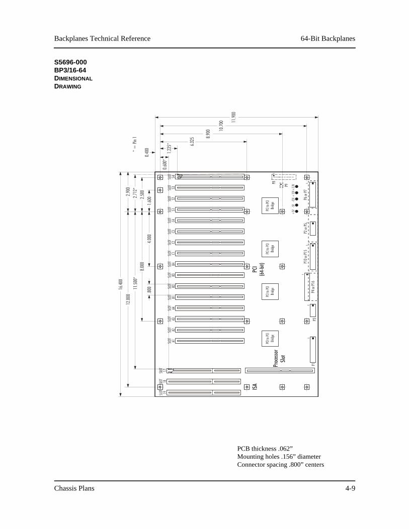
S5696-000 BP3/16-64
The BP3/16-64 is a PICMG-compatible backplane. It is a six-layer .062" thick PCB which provides two ISA slots, a dedicated SBC slot and 16 64-bit/33MHz PCI Local Bus slots for use by standard PCI Local Bus option cards.
The SBC slot supports SBCs with 32-bit/33MHz or 64-bit/33MHz PCI Bus extensions. The PCI slots support the PCI Local Bus 2.1 Specification. Twelve of the PCI slots are on the secondary PCI Bus, which is implemented using three Intel PCI-to-PCI bridges. The remaining four PCI slots are on the tertiary PCI Bus, which is implemented using a fourth Intel PCI-to-PCI bridge.
The standard AT power connection is available through two 12-pin .156 MTA connectors or one terminal block connector. Power connection for +3.3V is available through a 12-pin .156 MTA connector or an ATX connector (optional).
An extended-current option is also available. The extended-current connectors provide additional power capacity for power-intensive applications -- up to 150 Amps of +5V plus 150 Amps of +3.3V.
64-Bit Backplanes Backplanes Technical Reference
Chassis Plans4-8
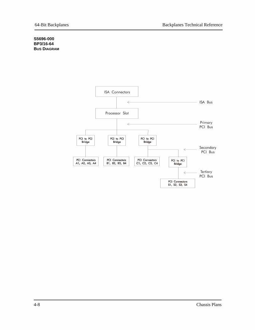
S5696-000 BP3/16-64 BUS DIAGRAM
64-Bit BackplanesBackplanes Technical Reference
Chassis Plans 4-9
S5696-000 BP3/16-64 DIMENSIONAL DRAWING
PCB thickness .062”Mounting holes .156” diameterConnector spacing .800” centers

64-Bit Backplanes Backplanes Technical Reference
Chassis Plans4-10
S5696-000 BP3/16-64 CONNECTORS
______________________________________________________________________
NOTE: Pin 1 on the connectors is indicated by the square pad on the PCB.______________________________________________________________________
P1 - Power Supply Connector12 pin right angle, Molex #26-60-5120
Pin123456789101112
SignalNC+5V+12V-12VGndGndGndGnd-5V+5V+5V+5V
P2 - +5V Extended-Current Connector (optional)5 pin right angle, Amp #193839-431 Amps per circuit(Refer to Amp Doc. #108-1594)
Pin12345
Signal+5V+5V+5V+5V+5V
P3 - Auxiliary Power Supply Connector6 pin right angle, Molex #26-60-5060
Pin123456
Signal+5V+5V+5VGndGndGnd
64-Bit BackplanesBackplanes Technical Reference
Chassis Plans 4-11
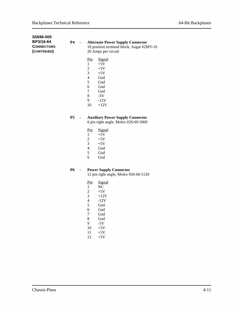
S5696-000 BP3/16-64 CONNECTORS (CONTINUED)
P4 - Alternate Power Supply Connector10 position terminal block, Augat #2MV-1020 Amps per circuit
Pin12345678910
Signal+5V+5V+5VGndGndGndGnd-5V-12V+12V
P5 - Auxiliary Power Supply Connector6 pin right angle, Molex #26-60-5060
Pin123456
Signal+5V+5V+5VGndGndGnd
P6 - Power Supply Connector12 pin right angle, Molex #26-60-5120
Pin123456789101112
SignalNC+5V+12V-12VGndGndGndGnd-5V+5V+5V+5V

64-Bit Backplanes Backplanes Technical Reference
Chassis Plans4-12
S5696-000 BP3/16-64 CONNECTORS (CONTINUED)
P7 - +5V Return Extended-Current Connector (optional)5 pin right angle, Amp #193839-431 Amps per circuit(Refer to Amp Doc. #108-1594)
Pin12345
SignalGndGndGndGndGnd
P8 - ATX Connector (optional)20 pin dual row header, Molex #39-29-9202
Pin12345678910
Signal+3.3V+3.3VGnd+5VGnd+5VGndPW-OK+5VSB+12V
Pin11121314151617181920
Signal+3.3V-12VGndPS-ONGndGndGnd-5V+5V+5V
P9 - ATX Power-On Connector (optional)2 pin header, Amp #640456-2
Pin12
SignalPS-ONGnd
P10 - +3.3V Power Supply Connector12 pin right angle, Molex #26-60-5120
Pin123456789101112
Signal+3.3V+3.3V+3.3VGndGndGndGndGndGnd+3.3V+3.3V+3.3V
64-Bit BackplanesBackplanes Technical Reference
Chassis Plans 4-13
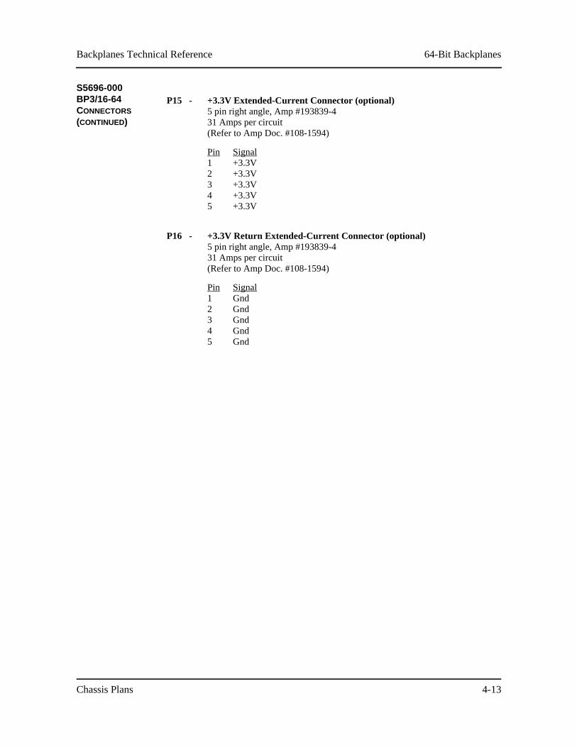
S5696-000 BP3/16-64 CONNECTORS (CONTINUED)
P15 - +3.3V Extended-Current Connector (optional)5 pin right angle, Amp #193839-431 Amps per circuit(Refer to Amp Doc. #108-1594)
Pin12345
Signal+3.3V+3.3V+3.3V+3.3V+3.3V
P16 - +3.3V Return Extended-Current Connector (optional)5 pin right angle, Amp #193839-431 Amps per circuit(Refer to Amp Doc. #108-1594)
Pin12345
SignalGndGndGndGndGnd

64-Bit Backplanes Backplanes Technical Reference
Chassis Plans4-14
This page intentionally left blank.
64-Bit BackplanesBackplanes Technical Reference
Chassis Plans 4-15
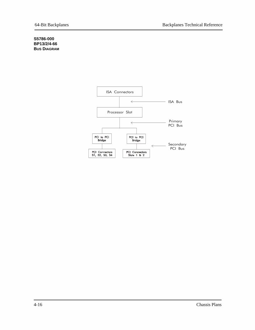
S5786-000 BP13/2/4-66
The BP13/2/4-66 is a PICMG-compatible backplane. It is a six-layer .062" thick PCB which provides 12 ISA slots, a 64-bit/66MHz SBC slot and six PCI Local Bus slots for use by standard PCI Local Bus option cards.
Of the six PCI Local Bus slots, two are 64-bit/66MHz PCI option slots and four are 64-bit/33MHz PCI option slots. Either 64-bit or 32-bit SBCs and option cards may be used. 64-bit and/or 66MHz option cards can take advantage of the 64-bit and/or 66MHz architecture when communicating with each other, even if a 32-bit SBC is used.
The PCI slots support the PCI Local Bus 2.1 Specification. Two of the PCI slots are on a secondary PCI Bus and are 64-bit/66MHz. These are +3.3V 64-bit PCI connectors on the backplane. Four of the PCI slots are 64-bit/33MHz and are on a secondary PCI Bus. These are +5V 64-bit PCI connectors on the backplane.
The standard AT power connection is available through two 12-pin .156 MTA connectors or one terminal block connector. Power connection for +3.3V is available through a 12-pin .156 MTA connector.
An extended-current option is also available. The extended-current connectors provide additional power capacity for power-intensive applications -- up to 150 Amps of +5V plus 150 Amps of +3.3V.
64-Bit Backplanes Backplanes Technical Reference
Chassis Plans4-16
S5786-000 BP13/2/4-66 BUS DIAGRAM
64-Bit BackplanesBackplanes Technical Reference
Chassis Plans 4-17
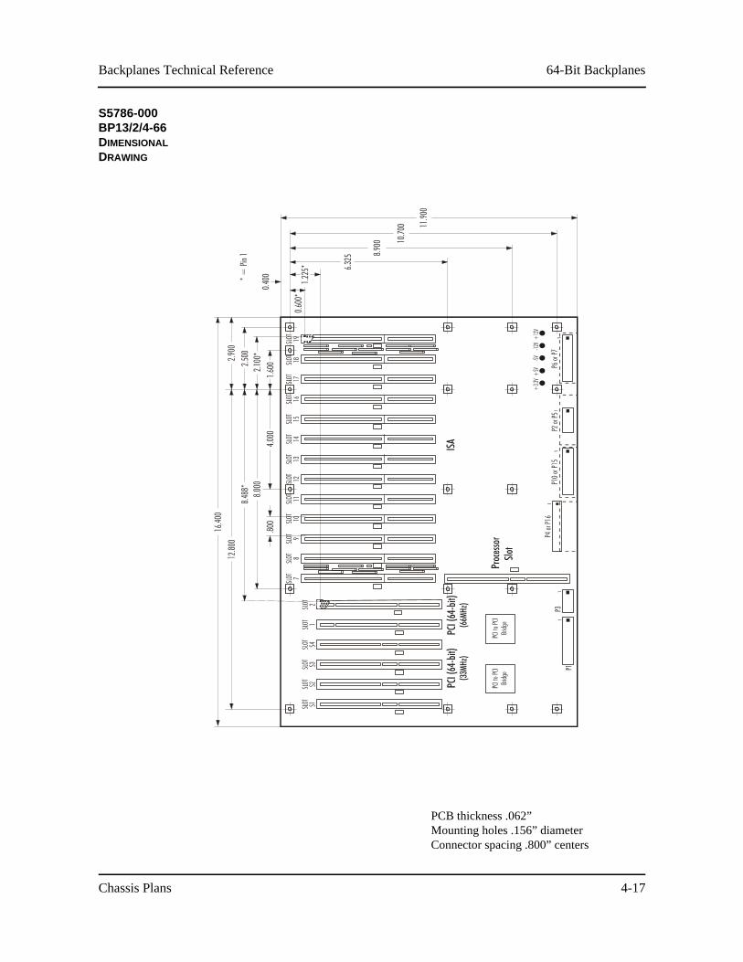
S5786-000 BP13/2/4-66 DIMENSIONAL DRAWING
PCB thickness .062”Mounting holes .156” diameterConnector spacing .800” centers
64-Bit Backplanes Backplanes Technical Reference
Chassis Plans4-18
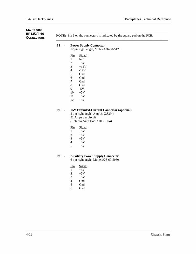
S5786-000 BP13/2/4-66 CONNECTORS
______________________________________________________________________
NOTE: Pin 1 on the connectors is indicated by the square pad on the PCB.______________________________________________________________________
P1 - Power Supply Connector12 pin right angle, Molex #26-60-5120
Pin123456789101112
SignalNC+5V+12V-12VGndGndGndGnd-5V+5V+5V+5V
P2 - +5V Extended-Current Connector (optional)5 pin right angle, Amp #193839-431 Amps per circuit(Refer to Amp Doc. #108-1594)
Pin12345
Signal+5V+5V+5V+5V+5V
P3 - Auxiliary Power Supply Connector6 pin right angle, Molex #26-60-5060
Pin123456
Signal+5V+5V+5VGndGndGnd
64-Bit BackplanesBackplanes Technical Reference
Chassis Plans 4-19
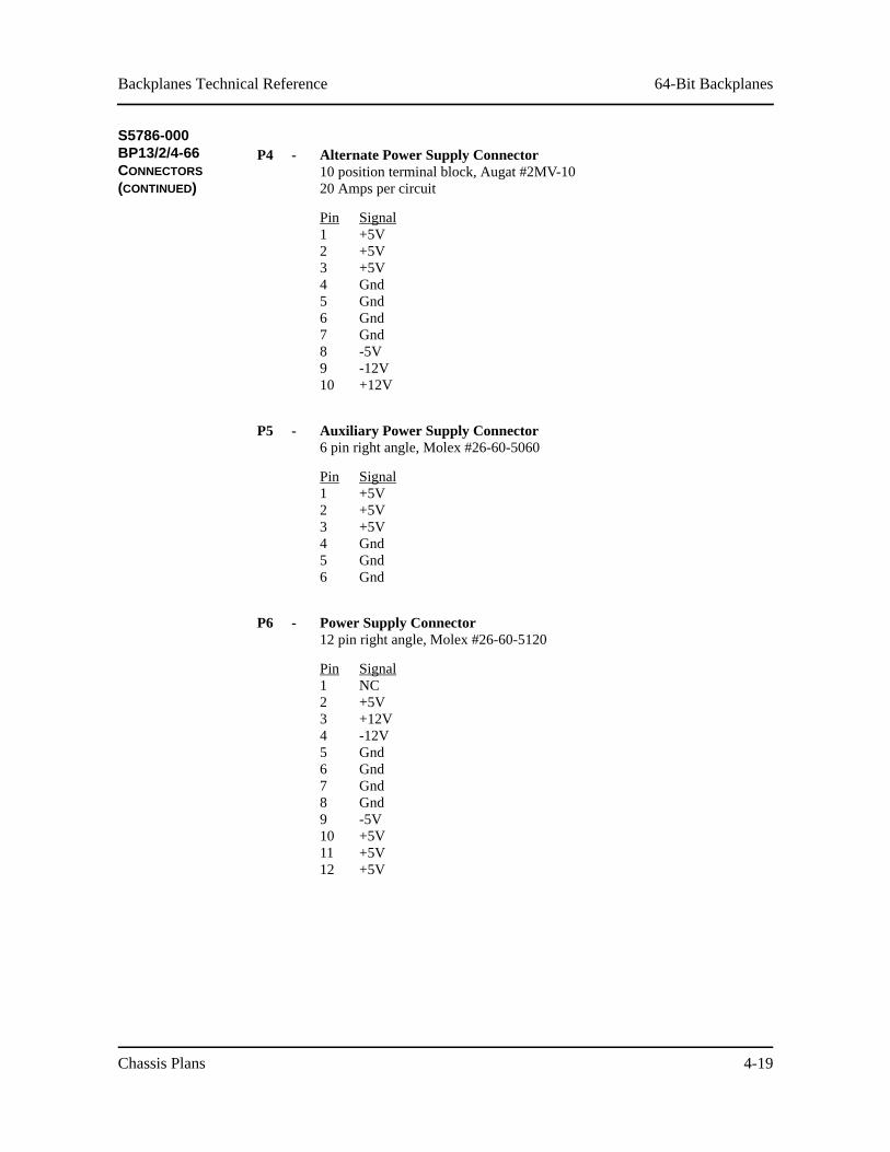
S5786-000 BP13/2/4-66 CONNECTORS (CONTINUED)
P4 - Alternate Power Supply Connector10 position terminal block, Augat #2MV-1020 Amps per circuit
Pin12345678910
Signal+5V+5V+5VGndGndGndGnd-5V-12V+12V
P5 - Auxiliary Power Supply Connector6 pin right angle, Molex #26-60-5060
Pin123456
Signal+5V+5V+5VGndGndGnd
P6 - Power Supply Connector12 pin right angle, Molex #26-60-5120
Pin123456789101112
SignalNC+5V+12V-12VGndGndGndGnd-5V+5V+5V+5V
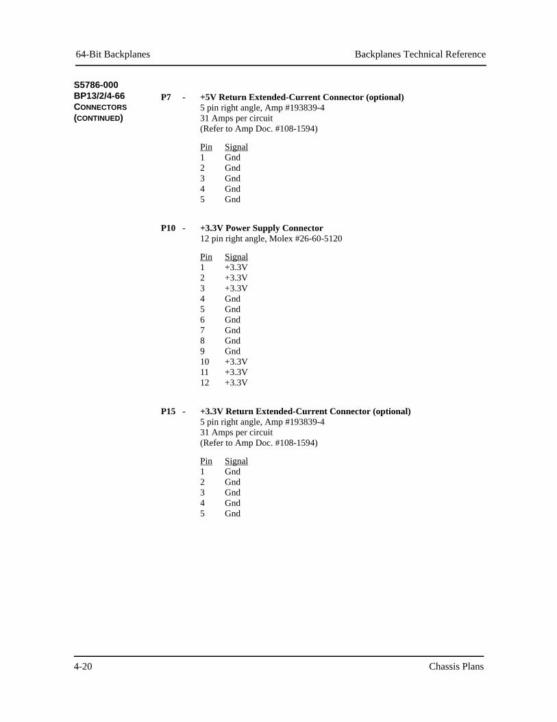
64-Bit Backplanes Backplanes Technical Reference
Chassis Plans4-20
S5786-000 BP13/2/4-66 CONNECTORS (CONTINUED)
P7 - +5V Return Extended-Current Connector (optional)5 pin right angle, Amp #193839-431 Amps per circuit(Refer to Amp Doc. #108-1594)
Pin12345
SignalGndGndGndGndGnd
P10 - +3.3V Power Supply Connector12 pin right angle, Molex #26-60-5120
Pin123456789101112
Signal+3.3V+3.3V+3.3VGndGndGndGndGndGnd+3.3V+3.3V+3.3V
P15 - +3.3V Return Extended-Current Connector (optional)5 pin right angle, Amp #193839-431 Amps per circuit(Refer to Amp Doc. #108-1594)
Pin12345
SignalGndGndGndGndGnd
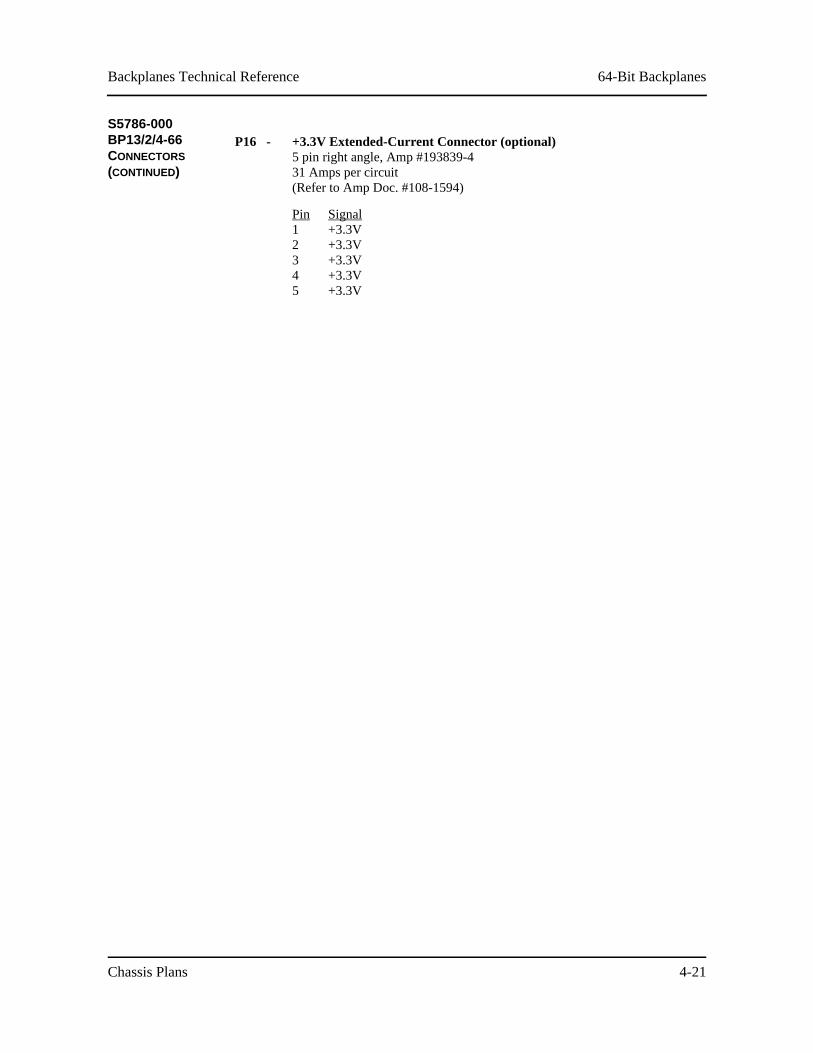
64-Bit BackplanesBackplanes Technical Reference
Chassis Plans 4-21
S5786-000 BP13/2/4-66 CONNECTORS (CONTINUED)
P16 - +3.3V Extended-Current Connector (optional)5 pin right angle, Amp #193839-431 Amps per circuit(Refer to Amp Doc. #108-1594)
Pin12345
Signal+3.3V+3.3V+3.3V+3.3V+3.3V

64-Bit Backplanes Backplanes Technical Reference
Chassis Plans4-22
This page intentionally left blank.
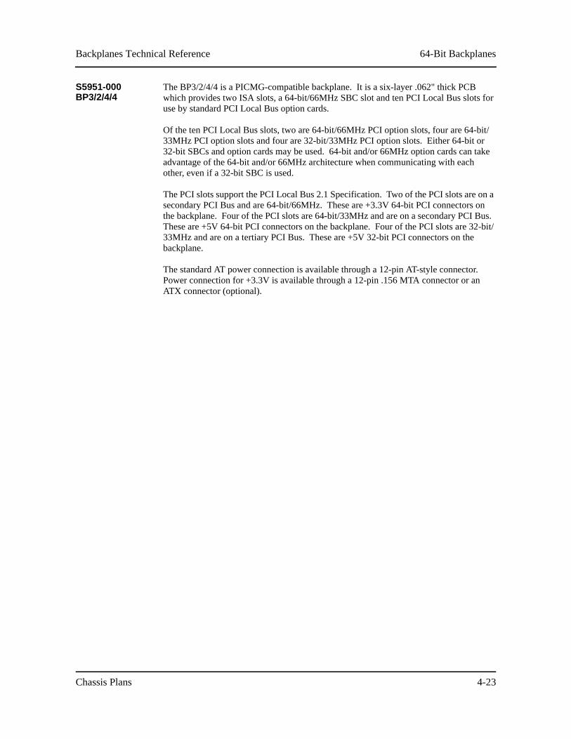
64-Bit BackplanesBackplanes Technical Reference
Chassis Plans 4-23
S5951-000 BP3/2/4/4
The BP3/2/4/4 is a PICMG-compatible backplane. It is a six-layer .062" thick PCB which provides two ISA slots, a 64-bit/66MHz SBC slot and ten PCI Local Bus slots for use by standard PCI Local Bus option cards.
Of the ten PCI Local Bus slots, two are 64-bit/66MHz PCI option slots, four are 64-bit/33MHz PCI option slots and four are 32-bit/33MHz PCI option slots. Either 64-bit or 32-bit SBCs and option cards may be used. 64-bit and/or 66MHz option cards can take advantage of the 64-bit and/or 66MHz architecture when communicating with each other, even if a 32-bit SBC is used.
The PCI slots support the PCI Local Bus 2.1 Specification. Two of the PCI slots are on a secondary PCI Bus and are 64-bit/66MHz. These are +3.3V 64-bit PCI connectors on the backplane. Four of the PCI slots are 64-bit/33MHz and are on a secondary PCI Bus. These are +5V 64-bit PCI connectors on the backplane. Four of the PCI slots are 32-bit/33MHz and are on a tertiary PCI Bus. These are +5V 32-bit PCI connectors on the backplane.
The standard AT power connection is available through a 12-pin AT-style connector. Power connection for +3.3V is available through a 12-pin .156 MTA connector or an ATX connector (optional).
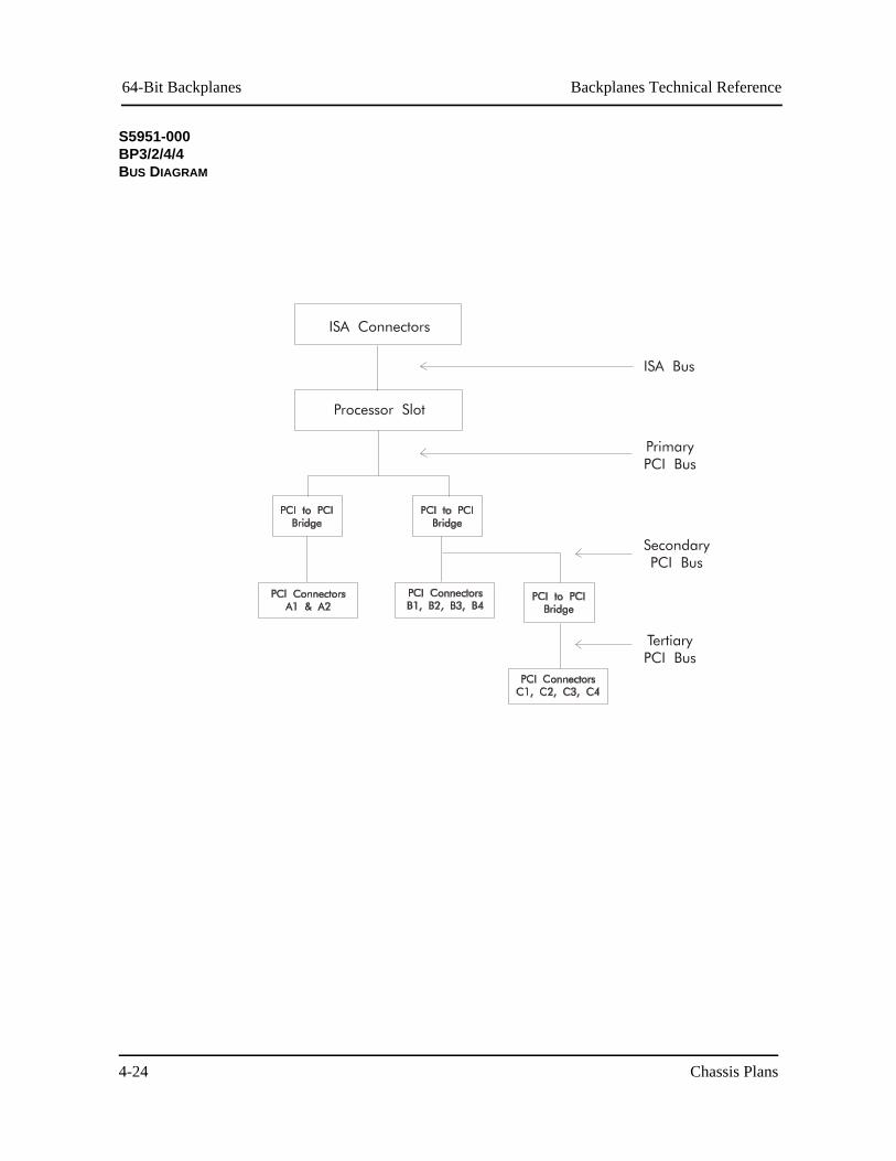
64-Bit Backplanes Backplanes Technical Reference
Chassis Plans4-24
S5951-000 BP3/2/4/4 BUS DIAGRAM
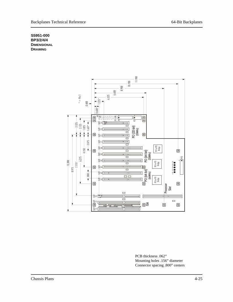
64-Bit BackplanesBackplanes Technical Reference
Chassis Plans 4-25
S5951-000 BP3/2/4/4 DIMENSIONAL DRAWING
PCB thickness .062”Mounting holes .156” diameterConnector spacing .800” centers

64-Bit Backplanes Backplanes Technical Reference
Chassis Plans4-26
S5951-000 BP3/2/4/4 CONNECTORS
______________________________________________________________________
NOTE: Pin 1 on the connectors is indicated by the square pad on the PCB.______________________________________________________________________
P1 - Power Supply Connector12 pin single row header, Leoco #4301P12V000
Pin123456789101112
SignalNC+5V+12V-12VGndGndGndGnd-5V+5V+5V+5V
P2 - Auxiliary Power Supply Connector6 pin single row header, Burndy #GTC6R-1
Pin123456
Signal+5V+5V+5VGndGndGnd
P9 - ATX Connector (optional)20 pin dual row header, Molex #39-29-9202
Pin12345678910
Signal+3.3V+3.3VGnd+5VGnd+5VGndPW-OK+5VSB+12V
Pin11121314151617181920
Signal+3.3V-12VGndPS-ONGndGndGnd-5V+5V+5V
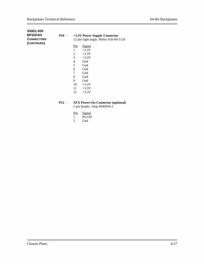
64-Bit BackplanesBackplanes Technical Reference
Chassis Plans 4-27
S5951-000 BP3/2/4/4 CONNECTORS (CONTINUED)
P10 - +3.3V Power Supply Connector12 pin right angle, Molex #26-60-5120
Pin123456789101112
Signal+3.3V+3.3V+3.3VGndGndGndGndGndGnd+3.3V+3.3V+3.3V
P12 - ATX Power-On Connector (optional)2 pin header, Amp #640456-2
Pin12
SignalPS-ONGnd

64-Bit Backplanes Backplanes Technical Reference
Chassis Plans4-28
This page intentionally left blank.

64-Bit BackplanesBackplanes Technical Reference
Chassis Plans 4-29
S5971-000 BP1/2
The BP1/2 is a PICMG-compatible backplane. It is a six-layer .062" thick PCB which provides one 64-bit/33MHz SBC slot and two PCI Local Bus slots for use by standard PCI Local Bus option cards.
The two PCI slots are 64-bit/33MHz PCI option slots which support the PCI Local Bus 2.1 Specification. Either 64-bit or 32-bit SBCs and option cards may be used.
Power connection is available through an ATX connector.

64-Bit Backplanes Backplanes Technical Reference
Chassis Plans4-30
S5971-000 BP1/2 BUS DIAGRAM
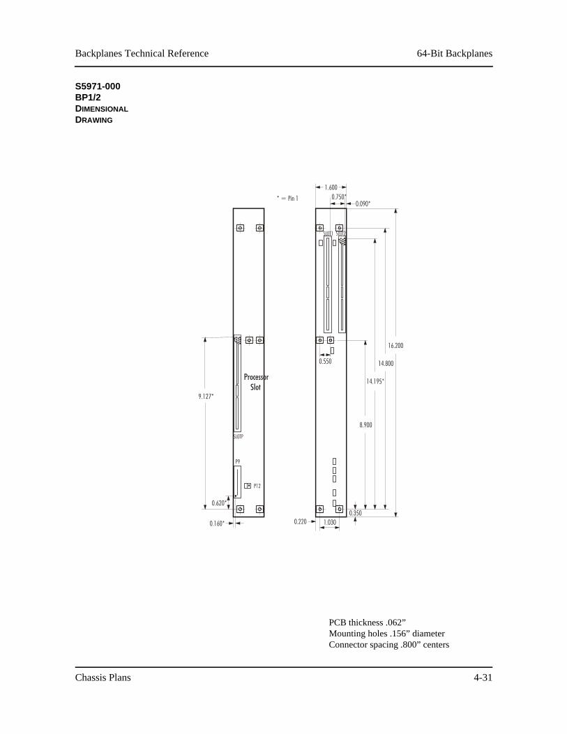
64-Bit BackplanesBackplanes Technical Reference
Chassis Plans 4-31
S5971-000 BP1/2 DIMENSIONAL DRAWING
PCB thickness .062”Mounting holes .156” diameterConnector spacing .800” centers
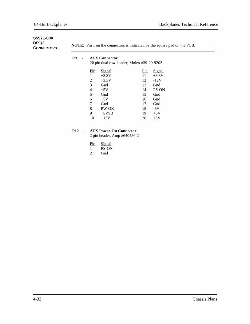
64-Bit Backplanes Backplanes Technical Reference
Chassis Plans4-32
S5971-000 BP1/2 CONNECTORS
______________________________________________________________________
NOTE: Pin 1 on the connectors is indicated by the square pad on the PCB.______________________________________________________________________
P9 - ATX Connector20 pin dual row header, Molex #39-29-9202
Pin12345678910
Signal+3.3V+3.3VGnd+5VGnd+5VGndPW-OK+5VSB+12V
Pin11121314151617181920
Signal+3.3V-12VGndPS-ONGndGndGnd-5V+5V+5V
P12 - ATX Power-On Connector2 pin header, Amp #640456-2
Pin12
SignalPS-ONGnd
64-Bit BackplanesBackplanes Technical Reference
Chassis Plans 4-33
S6195-000 BP3/6/4
The BP3/6/4 is a PICMG-compatible backplane. It is a six-layer .062" thick PCB which provides two ISA slots, a 64-bit/66MHz SBC slot and ten PCI Local Bus slots for use by standard PCI/ISA option cards.
Of the ten PCI Local Bus slots, six are 64-bit/66MHz PCI option slots and four are 64-bit/33MHz PCI option slots. Either 64-bit or 32-bit SBCs and option cards may be used. 64-bit and/or 66MHz option cards can take advantage of the 64-bit and/or 66MHz architecture when communicating with each other, even if a 32-bit SBC is used.
The PCI slots support the PCI Local Bus 2.1 Specification. The six 64-bit/66MHz PCI slots are +3.3V 64-bit PCI connectors on the backplane and the four 64-bit/33MHz PCI slots are +5V 64-bit PCI connectors. A total of five Intel PCI-to-PCI bridges are used in the backplane’s architecture.
The standard AT power connection is available through a 12-pin .156 MTA connector. Power connection for +3.3V is available through a 12-pin .156 MTA connector or an ATX connector (optional).
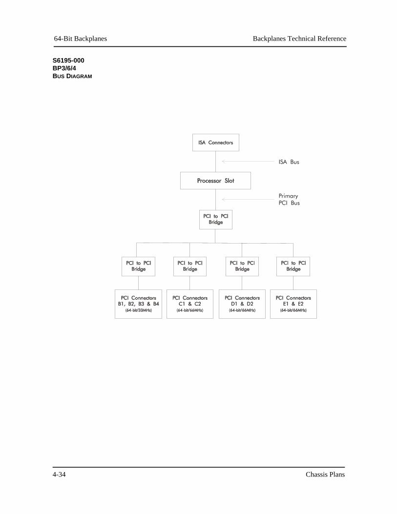
64-Bit Backplanes Backplanes Technical Reference
Chassis Plans4-34
S6195-000 BP3/6/4 BUS DIAGRAM
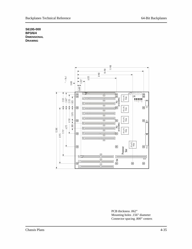
64-Bit BackplanesBackplanes Technical Reference
Chassis Plans 4-35
S6195-000 BP3/6/4 DIMENSIONAL DRAWING
PCB thickness .062”Mounting holes .156” diameterConnector spacing .800” centers
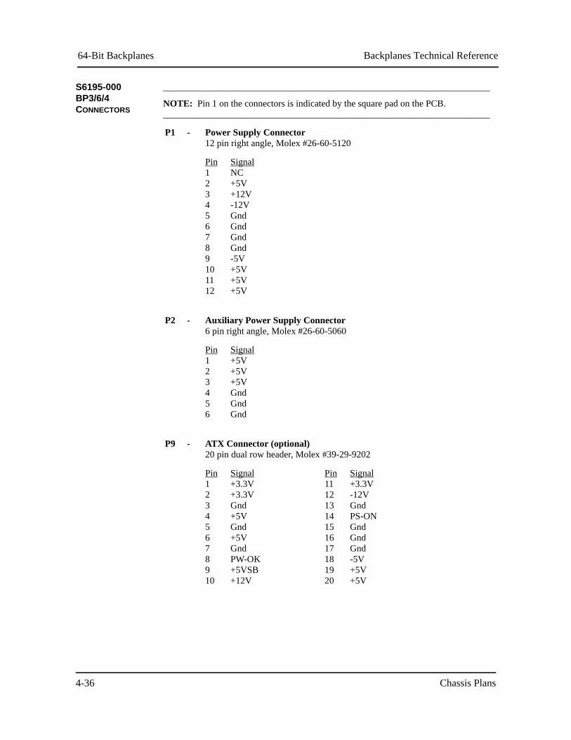
64-Bit Backplanes Backplanes Technical Reference
Chassis Plans4-36
S6195-000 BP3/6/4 CONNECTORS
______________________________________________________________________
NOTE: Pin 1 on the connectors is indicated by the square pad on the PCB.______________________________________________________________________
P1 - Power Supply Connector12 pin right angle, Molex #26-60-5120
Pin123456789101112
SignalNC+5V+12V-12VGndGndGndGnd-5V+5V+5V+5V
P2 - Auxiliary Power Supply Connector6 pin right angle, Molex #26-60-5060
Pin123456
Signal+5V+5V+5VGndGndGnd
P9 - ATX Connector (optional)20 pin dual row header, Molex #39-29-9202
Pin12345678910
Signal+3.3V+3.3VGnd+5VGnd+5VGndPW-OK+5VSB+12V
Pin11121314151617181920
Signal+3.3V-12VGndPS-ONGndGndGnd-5V+5V+5V
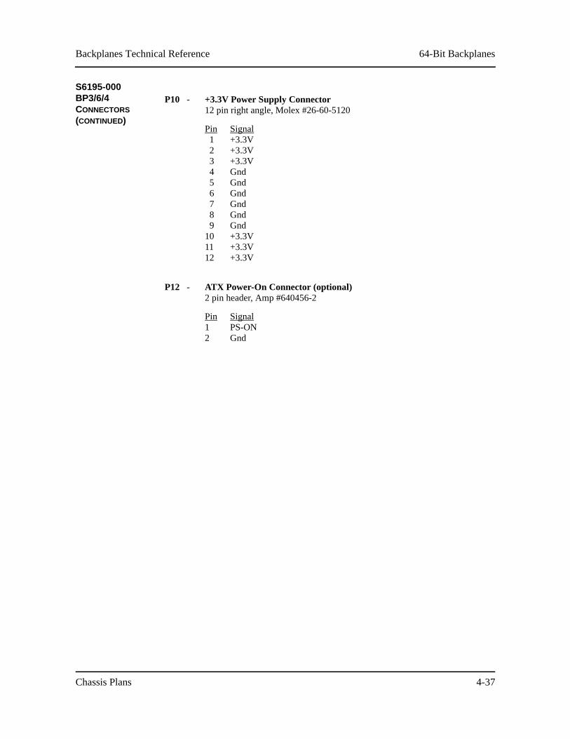
64-Bit BackplanesBackplanes Technical Reference
Chassis Plans 4-37
S6195-000 BP3/6/4 CONNECTORS (CONTINUED)
P10 - +3.3V Power Supply Connector12 pin right angle, Molex #26-60-5120
Pin123456789
101112
Signal+3.3V+3.3V+3.3VGndGndGndGndGndGnd+3.3V+3.3V+3.3V
P12 - ATX Power-On Connector (optional)2 pin header, Amp #640456-2
Pin12
SignalPS-ONGnd
64-Bit Backplanes Backplanes Technical Reference
Chassis Plans4-38
This page intentionally left blank.
Copyright 2006 by Trenton Technology Inc. All rights reserved.
Segmented BackplanesBackplanes Technical Reference
Chassis Plans 5-1
Chapter 5 Segmented Backplanes
S5574-000 BP2S13
The BP2S13 is a 13-slot PICMG-compatible backplane. It is a six-layer .062" thick PCB which is divided into two segments, with each segment operating independently and consisting of an ISA Bus and a PCI Local Bus. The two segments share the same power source. All of the PCI Local Bus slots support the PCI Local Bus 2.1 Specification.
One of the segments provides one ISA slot which is dedicated to the SBC with PCI extension, three additional ISA Bus slots for the use of standard ISA Bus option cards and three PCI Local Bus slots for the use of standard PCI Local Bus option cards.
The other segment provides one ISA slot dedicated to the SBC with PCI extension, two additional ISA Bus slots and three PCI Local Bus slots.
The standard AT power connection is available through a 12-pin AT-style connector or a terminal block connector. Power connection for +3.3V is available through a 12-pin AT-style connector or an ATX connector (optional).
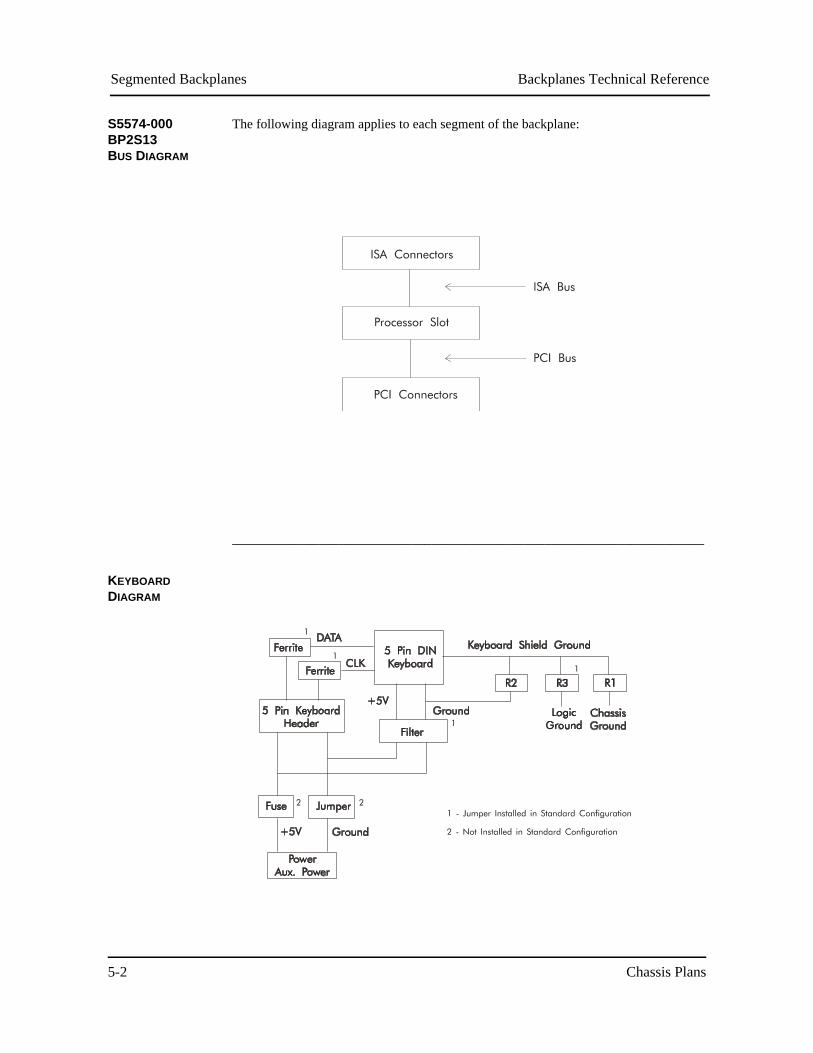
Segmented Backplanes Backplanes Technical Reference
Chassis Plans5-2
S5574-000 BP2S13 BUS DIAGRAM
The following diagram applies to each segment of the backplane:
_______________________________________________________________________
KEYBOARD DIAGRAM
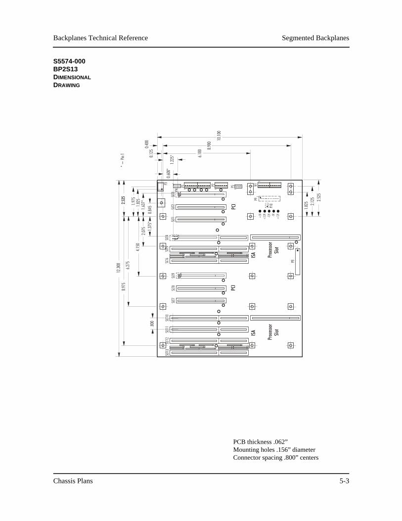
Segmented BackplanesBackplanes Technical Reference
Chassis Plans 5-3
S5574-000 BP2S13 DIMENSIONAL DRAWING
PCB thickness .062”Mounting holes .156” diameterConnector spacing .800” centers
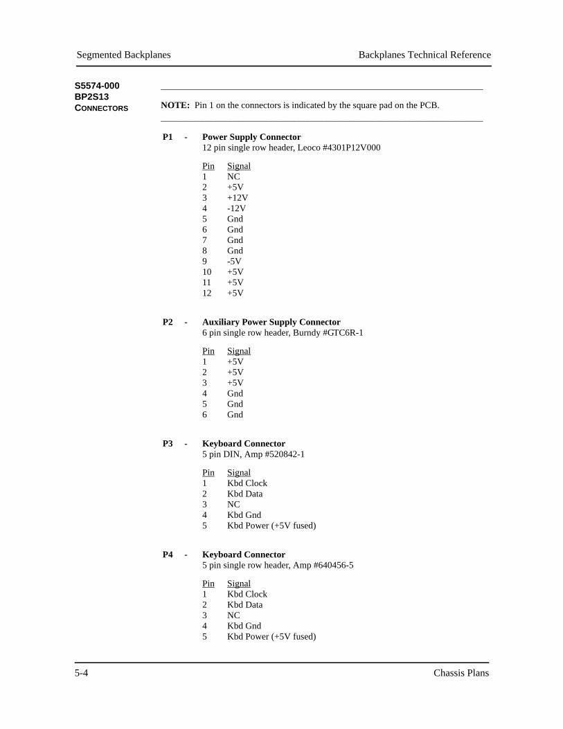
Segmented Backplanes Backplanes Technical Reference
Chassis Plans5-4
S5574-000 BP2S13 CONNECTORS
______________________________________________________________________
NOTE: Pin 1 on the connectors is indicated by the square pad on the PCB.______________________________________________________________________
P1 - Power Supply Connector12 pin single row header, Leoco #4301P12V000
Pin123456789101112
SignalNC+5V+12V-12VGndGndGndGnd-5V+5V+5V+5V
P2 - Auxiliary Power Supply Connector6 pin single row header, Burndy #GTC6R-1
Pin123456
Signal+5V+5V+5VGndGndGnd
P3 - Keyboard Connector5 pin DIN, Amp #520842-1
Pin12345
SignalKbd ClockKbd DataNCKbd GndKbd Power (+5V fused)
P4 - Keyboard Connector5 pin single row header, Amp #640456-5
Pin12345
SignalKbd ClockKbd DataNCKbd GndKbd Power (+5V fused)
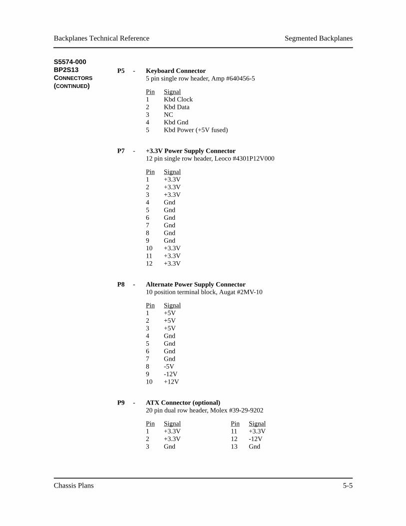
Segmented BackplanesBackplanes Technical Reference
Chassis Plans 5-5
S5574-000 BP2S13 CONNECTORS (CONTINUED)
P5 - Keyboard Connector5 pin single row header, Amp #640456-5
Pin12345
SignalKbd ClockKbd DataNCKbd GndKbd Power (+5V fused)
P7 - +3.3V Power Supply Connector12 pin single row header, Leoco #4301P12V000
Pin123456789101112
Signal+3.3V+3.3V+3.3VGndGndGndGndGndGnd+3.3V+3.3V+3.3V
P8 - Alternate Power Supply Connector10 position terminal block, Augat #2MV-10
Pin12345678910
Signal+5V+5V+5VGndGndGndGnd-5V-12V+12V
P9 - ATX Connector (optional)20 pin dual row header, Molex #39-29-9202
Pin123
Signal+3.3V+3.3VGnd
Pin111213
Signal+3.3V-12VGnd
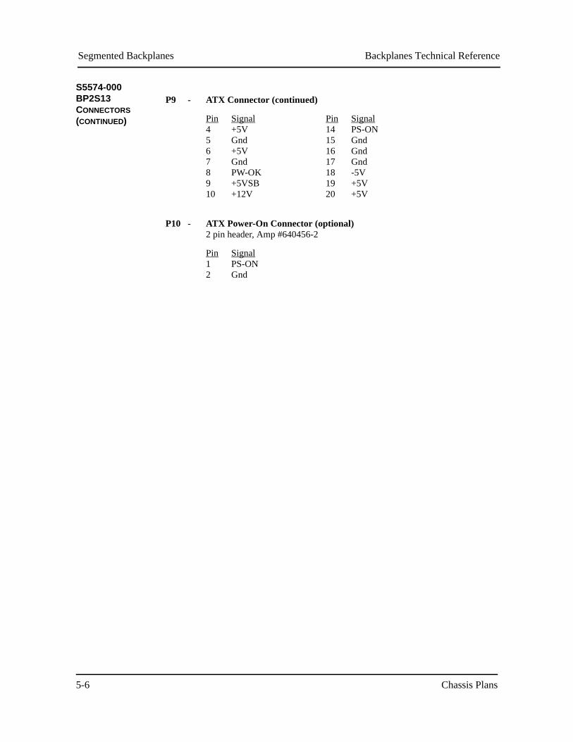
Segmented Backplanes Backplanes Technical Reference
Chassis Plans5-6
S5574-000 BP2S13 CONNECTORS (CONTINUED)
P9 - ATX Connector (continued)
Pin45678910
Signal+5VGnd+5VGndPW-OK +5VSB+12V
Pin14151617181920
SignalPS-ONGndGndGnd-5V+5V+5V
P10 - ATX Power-On Connector (optional)2 pin header, Amp #640456-2
Pin12
SignalPS-ONGnd
Segmented BackplanesBackplanes Technical Reference
Chassis Plans 5-7
S5577-000 BP2S19
The BP2S19 is a 19-slot PICMG-compatible backplane. It is a six-layer .062" thick PCB which is divided into two segments, with each segment operating independently and consisting of an ISA Bus and a PCI Local Bus. The two segments share the same power source. All of the PCI Local Bus slots support the PCI Local Bus 2.1 Specification.
One of the segments provides one ISA slot which is dedicated to the SBC with PCI extension, six additional ISA Bus slots for the use of standard ISA Bus option cards and three PCI Local Bus slots for the use of standard PCI Local Bus option cards.
The other segment provides one ISA slot dedicated to the SBC with PCI extension, five additional ISA Bus slots and three PCI Local Bus slots.
The standard AT power connection is available through two 12-pin .156 MTA connectors or one terminal block connector. Power connection for +3.3V is available through a 12-pin .156 MTA connector or an ATX connector (optional).
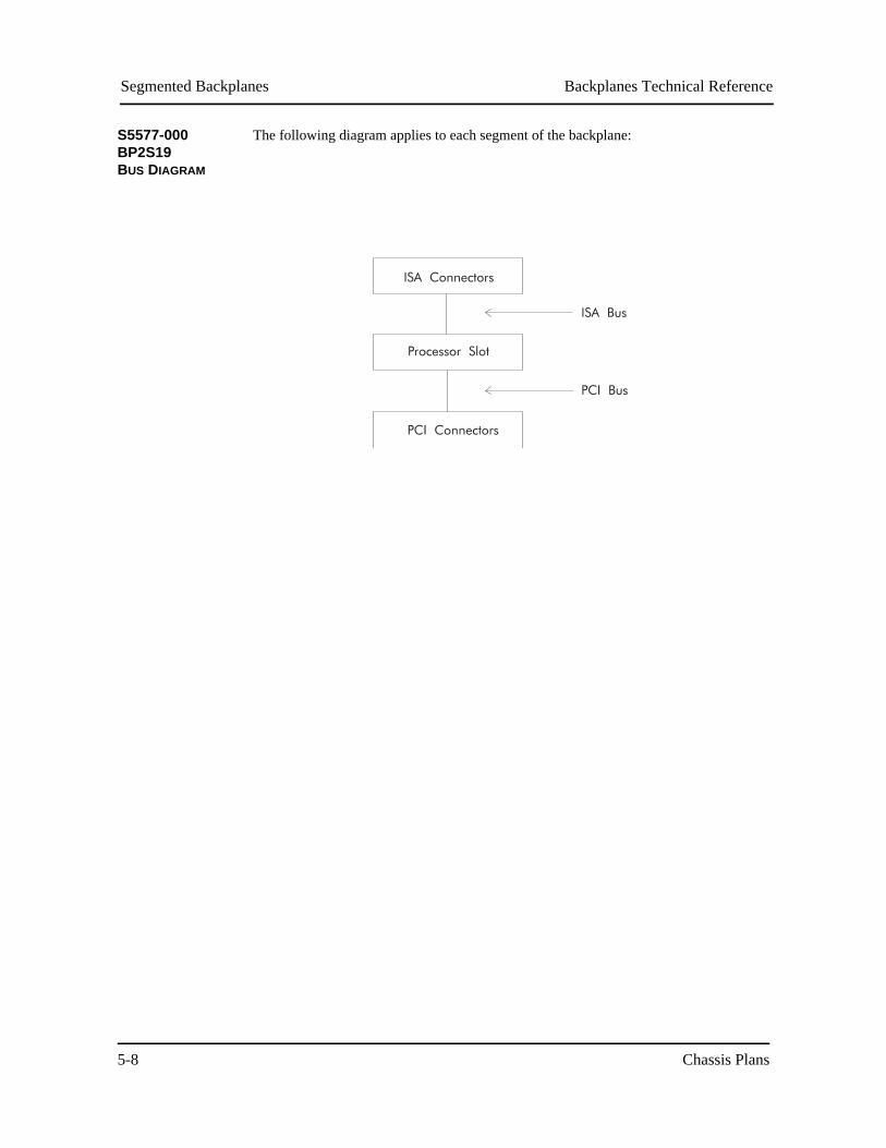
Segmented Backplanes Backplanes Technical Reference
Chassis Plans5-8
S5577-000 BP2S19 BUS DIAGRAM
The following diagram applies to each segment of the backplane:
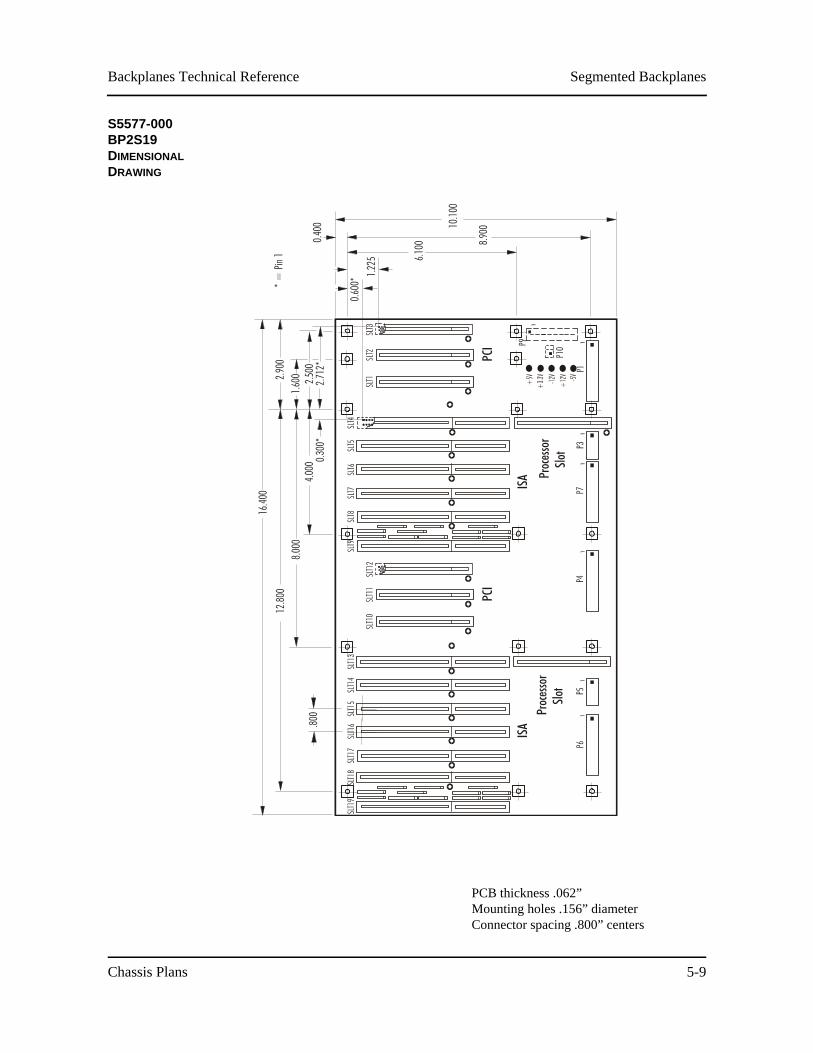
Segmented BackplanesBackplanes Technical Reference
Chassis Plans 5-9
S5577-000 BP2S19 DIMENSIONAL DRAWING
PCB thickness .062”Mounting holes .156” diameterConnector spacing .800” centers
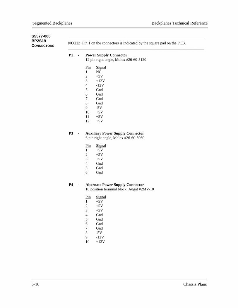
Segmented Backplanes Backplanes Technical Reference
Chassis Plans5-10
S5577-000 BP2S19 CONNECTORS
______________________________________________________________________
NOTE: Pin 1 on the connectors is indicated by the square pad on the PCB.______________________________________________________________________
P1 - Power Supply Connector12 pin right angle, Molex #26-60-5120
Pin123456789101112
SignalNC+5V+12V-12VGndGndGndGnd-5V+5V+5V+5V
P3 - Auxiliary Power Supply Connector6 pin right angle, Molex #26-60-5060
Pin123456
Signal+5V+5V+5VGndGndGnd
P4 - Alternate Power Supply Connector10 position terminal block, Augat #2MV-10
Pin12345678910
Signal+5V+5V+5VGndGndGndGnd-5V-12V+12V

Segmented BackplanesBackplanes Technical Reference
Chassis Plans 5-11
S5577-000 BP2S19 CONNECTORS (CONTINUED)
P5 - Auxiliary Power Supply Connector6 pin right angle, Molex #26-60-5060
Pin123456
Signal+5V+5V+5VGndGndGnd
P6 - Power Supply Connector12 pin right angle, Molex #26-60-5120
Pin123456789101112
SignalNC+5V+12V-12VGndGndGndGnd-5V+5V+5V+5V
P7 - +3.3V Power Supply Connector12 pin right angle, Molex #26-60-5120
Pin123456789101112
Signal+3.3V+3.3V+3.3VGndGndGndGndGndGnd+3.3V+3.3V+3.3V
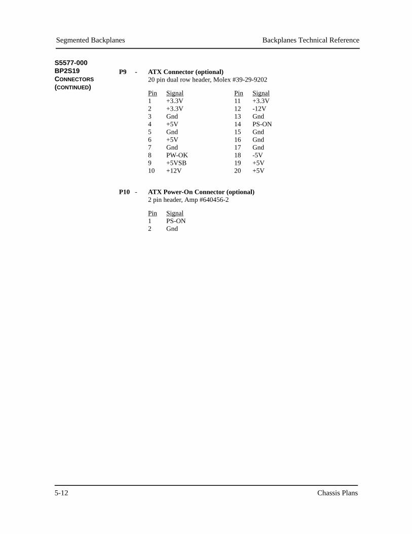
Segmented Backplanes Backplanes Technical Reference
Chassis Plans5-12
S5577-000 BP2S19 CONNECTORS (CONTINUED)
Copyright 2006 by Trenton Technology Inc. All rights reserved.
P9 - ATX Connector (optional)20 pin dual row header, Molex #39-29-9202
Pin12345678910
Signal+3.3V+3.3V Gnd+5VGnd+5VGndPW-OK +5VSB+12V
Pin11121314151617181920
Signal+3.3V-12VGndPS-ONGndGndGnd-5V+5V+5V
P10 - ATX Power-On Connector (optional)2 pin header, Amp #640456-2
Pin12
SignalPS-ON Gnd
PCI-X BackplanesBackplanes Technical Reference
Chassis Plans 6-1
Chapter 6 PCI-X Backplanes
S6120-000 BP1/1/2/4/4
The BP1/1/2/4/4 is a PICMG-compatible backplane. It is an eight-layer .062" thick PCB which provides an SBC slot which can run up to 64-bit/133MHz and 11 PCI-X/PCI Local Bus slots for use by standard PCI-X and PCI option cards.
Of the 11 PCI-X/PCI Local Bus slots, one is a 64-bit/133MHz PCI-X option slot, two are 64-bit/100MHz PCI-X option slots, four are 64-bit/66MHz PCI-X option slots and four are 64-bit/33MHz PCI option slots.
The standard AT power connection is available through a 12-pin .156 MTA connector. Power connection for +3.3V is available through a 12-pin .156 MTA connector or an ATX connector (optional).
An extended-current option is also available. The extended-current connectors provide additional power capacity for power-intensive applications -- up to 60 Amps of +5V plus 60 Amps of +3.3V.
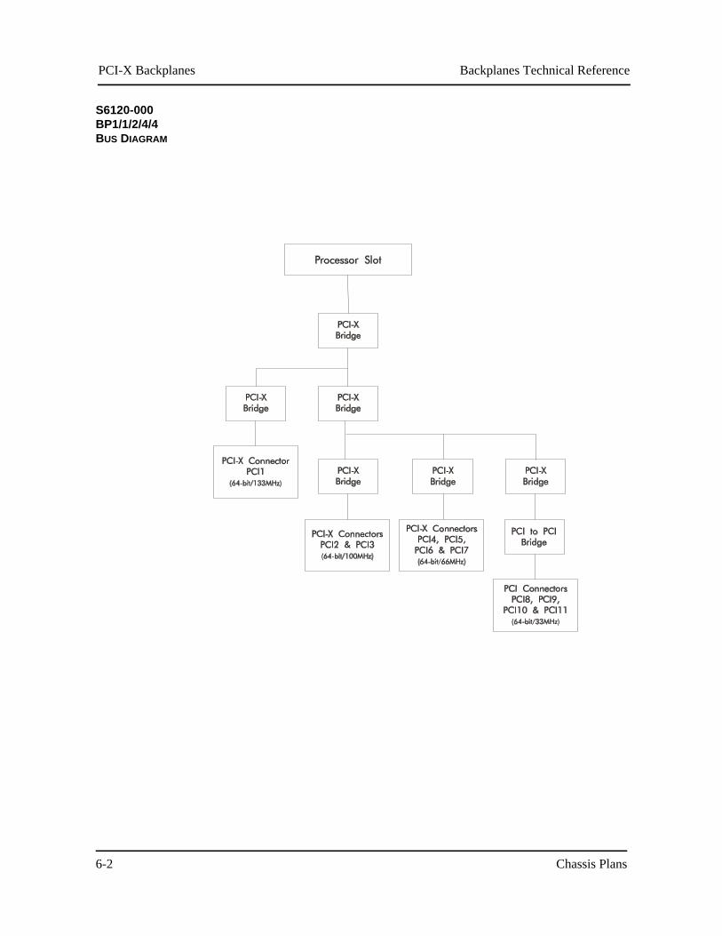
PCI-X Backplanes Backplanes Technical Reference
Chassis Plans6-2
S6120-000 BP1/1/2/4/4 BUS DIAGRAM
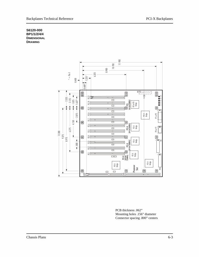
PCI-X BackplanesBackplanes Technical Reference
Chassis Plans 6-3
S6120-000 BP1/1/2/4/4 DIMENSIONAL DRAWING
PCB thickness .062”Mounting holes .156” diameterConnector spacing .800” centers
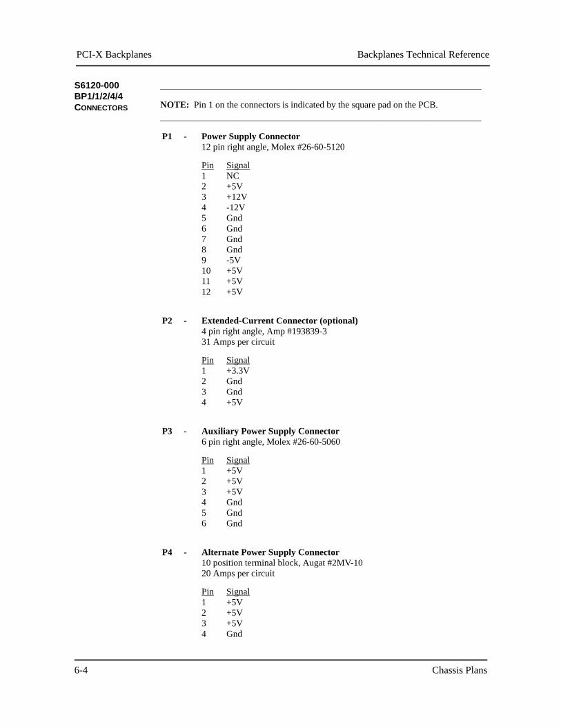
PCI-X Backplanes Backplanes Technical Reference
Chassis Plans6-4
S6120-000 BP1/1/2/4/4 CONNECTORS
______________________________________________________________________
NOTE: Pin 1 on the connectors is indicated by the square pad on the PCB.______________________________________________________________________
P1 - Power Supply Connector12 pin right angle, Molex #26-60-5120
Pin123456789101112
SignalNC+5V+12V-12VGndGndGndGnd-5V+5V+5V+5V
P2 - Extended-Current Connector (optional)4 pin right angle, Amp #193839-331 Amps per circuit
Pin1234
Signal+3.3VGndGnd+5V
P3 - Auxiliary Power Supply Connector6 pin right angle, Molex #26-60-5060
Pin123456
Signal+5V+5V+5VGndGndGnd
P4 - Alternate Power Supply Connector10 position terminal block, Augat #2MV-1020 Amps per circuit
Pin1234
Signal+5V+5V+5VGnd
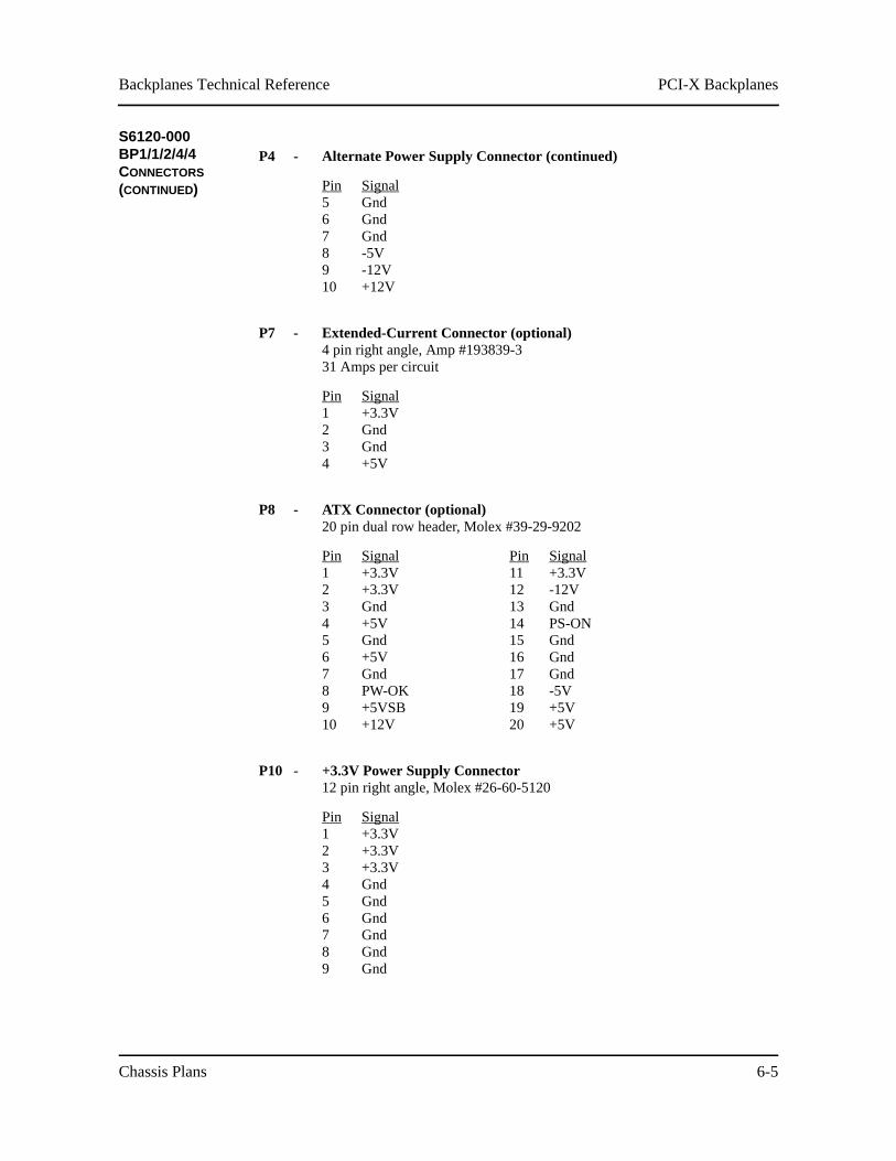
PCI-X BackplanesBackplanes Technical Reference
Chassis Plans 6-5
S6120-000 BP1/1/2/4/4 CONNECTORS (CONTINUED)
P4 - Alternate Power Supply Connector (continued)
Pin5678910
SignalGndGndGnd-5V-12V+12V
P7 - Extended-Current Connector (optional)4 pin right angle, Amp #193839-331 Amps per circuit
Pin1234
Signal+3.3VGndGnd+5V
P8 - ATX Connector (optional)20 pin dual row header, Molex #39-29-9202
Pin12345678910
Signal+3.3V+3.3VGnd+5VGnd+5VGndPW-OK+5VSB+12V
Pin11121314151617181920
Signal+3.3V-12VGndPS-ONGndGndGnd-5V+5V+5V
P10 - +3.3V Power Supply Connector12 pin right angle, Molex #26-60-5120
Pin123456789
Signal+3.3V+3.3V+3.3VGndGndGndGndGndGnd

PCI-X Backplanes Backplanes Technical Reference
Chassis Plans6-6
S6120-000 BP1/1/2/4/4 CONNECTORS (CONTINUED)
Copyright 2006 by Trenton Technology Inc. All rights reserved.
P10 - +3.3V Power Supply Connector (continued)
Pin101112
Signal+3.3V+3.3V+3.3V
P14 - ATX Power-On Connector (optional)2 pin header, Amp #640456-2
Pin12
SignalPS-ONGnd