picmg 2.0 d3.0 compactpci specification - · pdf filecompactpci® core specification picmg...
TRANSCRIPT

PICMG 2.0 D3.0
CompactPCI CompactPCI CompactPCI CompactPCI SpecificationSeptember 24, 1999
DRAFT SPECIFICATIONDO NOT CLAIM CONFORMANCE

PICMG 2.0 D3.0 9/24/99Draft, Not for Distribution – Do Not Claim Conformance
ii
Copyright 1995, 1996, 1997, 1998, 1999 PCI Industrial Computers ManufacturersGroup (PICMG).
The attention of adopters is directed to the possibility that compliance with or adoption ofPICMG specifications may require use of an invention covered by patent rights.PICMG shall not be responsible for identifying patents for which a license may berequired by any PICMG specification, or for conducting legal inquiries into the legalvalidity or scope of those patents that are brought to its attention. PICMG specificationsare prospective and advisory only. Prospective users are responsible for protectingthemselves against liability for infringement of patents.
NOTICE:The information contained in this document is subject to change without notice. Thematerial in this document details a PICMG specification in accordance with the licenseand notices set forth on this page. This document does not represent a commitment toimplement any portion of this specification in any company's products.
WHILE THE INFORMATION IN THIS PUBLICATION IS BELIEVED TO BEACCURATE, PICMG MAKES NO WARRANTY OF ANY KIND, EXPRESS ORIMPLIED, WITH REGARD TO THIS MATERIAL INCLUDING, BUT NOT LIMITEDTO ANY WARRANTY OF TITLE OR OWNERSHIP, IMPLIED WARRANTY OFMERCHANTABILITY OR WARRANTY OF FITNESS FOR PARTICULARPURPOSE OR USE.
In no event shall PICMG be liable for errors contained herein or for indirect, incidental,special, consequential, reliance or cover damages, including loss of profits, revenue, dataor use, incurred by any user or any third party.
Compliance with this specification does not absolve manufacturers of CompactPCIequipment, from the requirements of safety and regulatory agencies (UL, CSA, FCC,IEC, etc.).PICMG, CompactPCI, and the PICMG and CompactPCI logos are registeredtrademarks of the PCI Industrial Computers Manufacturers Group.
All other brand or product names may be trademarks or registered trademarks of their re-spective holders.

CompactPCI® Core Specification PICMG 2.0 D3.0 9/24/99 iiiDraft for PICMG Executive ApprovalDo not specify or claim conformance to this specification - Not for Distribution
Contents1 OVERVIEW ........................................................................................................................................ 91.1 COMPACTPCI OBJECTIVES................................................................................................................ 91.2 BACKGROUND AND TERMINOLOGY................................................................................................... 91.3 DESIRED AUDIENCE .......................................................................................................................... 91.4 COMPACTPCI FEATURES ................................................................................................................ 101.5 APPLICABLE DOCUMENTS ............................................................................................................... 101.6 ADMINISTRATION ............................................................................................................................ 111.7 NAME AND LOGO USAGE................................................................................................................ 122 FEATURE SET ................................................................................................................................. 132.1 FORM FACTOR................................................................................................................................. 132.2 CONNECTOR.................................................................................................................................... 152.3 MODULARITY .................................................................................................................................. 162.4 HOT SWAP CAPABILITY ................................................................................................................... 163 ELECTRICAL REQUIREMENTS................................................................................................. 173.1 BOARD DESIGN RULES .................................................................................................................... 17
3.1.1 Decoupling Requirements..................................................................................................... 173.1.2 CompactPCI Signal Additions .............................................................................................. 183.1.3 CompactPCI Stub Termination............................................................................................. 183.1.4 Peripheral Board Signal Stub Length................................................................................... 183.1.5 Characteristic Impedance..................................................................................................... 193.1.6 System Slot Board Signal Stub Length.................................................................................. 193.1.7 Peripheral Board PCI Clock Signal Length ......................................................................... 193.1.8 Pull-Up Location .................................................................................................................. 193.1.9 Board Connector Shield Requirements................................................................................. 20
3.2 BACKPLANE DESIGN RULES ............................................................................................................ 213.2.1 Characteristic Impedance..................................................................................................... 213.2.2 Eight-Slot Backplane Termination........................................................................................ 213.2.3 Signaling Environment ......................................................................................................... 223.2.4 IDSEL Assignment ................................................................................................................ 223.2.5 REQ#/GNT# Assignment ...................................................................................................... 233.2.6 PCI Interrupt Binding........................................................................................................... 243.2.7 CompactPCI Signal Additions .............................................................................................. 253.2.8 Power Distribution................................................................................................................ 283.2.9 Power Decoupling ................................................................................................................ 303.2.10 Healthy (Healthy#) ............................................................................................................... 31
3.3 33 MHZ PCI CLOCK DISTRIBUTION ................................................................................................ 313.3.1 Backplane Clock Routing Design Rules................................................................................ 323.3.2 System Slot Board Clock Routing Design Rules ................................................................... 32
3.4 64-BIT DESIGN RULES..................................................................................................................... 333.5 66 MHZ ELECTRICAL REQUIREMENTS ............................................................................................ 35
3.5.1 66 MHz Board Design Rules................................................................................................. 353.5.2 66 MHz System Board Design Rules..................................................................................... 353.5.3 66MHz Backplane Design Rules........................................................................................... 353.5.4 66MHz PCI Clock Distribution............................................................................................. 353.5.5 66 MHz System Slot Board Clock Routing Design Rules...................................................... 363.5.6 66 MHz Hot Swap ................................................................................................................. 37
3.6 SYSTEM AND BOARD GROUNDING .................................................................................................. 373.6.1 Board Front Panel Grounding Requirements....................................................................... 373.6.2 Backplane Grounding Requirements .................................................................................... 37
3.7 COMPACTPCI BUFFER MODELS...................................................................................................... 37

PICMG 2.0 D3.0 9/24/99Draft, Not for Distribution – Do Not Claim Conformance
iv
4 MECHANICAL REQUIREMENTS ............................................................................................... 394.1 BOARD REQUIREMENTS .................................................................................................................. 39
4.1.1 3U Boards............................................................................................................................. 394.1.2 6U Boards............................................................................................................................. 394.1.3 Rear-panel I/O Boards.......................................................................................................... 394.1.4 ESD Discharge Strip............................................................................................................. 404.1.5 ESD Clip ............................................................................................................................... 404.1.6 Cross Sectional View ............................................................................................................ 414.1.7 Component Outline and Warpage ........................................................................................ 414.1.8 Solder Side Cover ................................................................................................................. 414.1.9 Front Panels ......................................................................................................................... 514.1.10 System Slot Identification...................................................................................................... 52
4.2 REAR-PANEL I/O BOARD REQUIREMENTS ...................................................................................... 554.2.1 Mechanicals .......................................................................................................................... 554.2.2 Power.................................................................................................................................... 554.2.3 Rear Panel Keying ................................................................................................................ 56
4.3 BACKPLANE REQUIREMENTS........................................................................................................... 564.3.1 Connector Orientation .......................................................................................................... 564.3.2 Slot Spacing .......................................................................................................................... 564.3.3 Slot Designation.................................................................................................................... 574.3.4 Bus Segments ........................................................................................................................ 574.3.5 Backplane Dimensions.......................................................................................................... 57
5 CONNECTOR IMPLEMENTATION............................................................................................ 615.1 OVERVIEW ...................................................................................................................................... 62
5.1.1 Location ................................................................................................................................ 625.1.2 Housing Types....................................................................................................................... 625.1.3 Connector Tail Lengths......................................................................................................... 625.1.4 Backplane / Board Population Options ................................................................................ 62
5.2 J1 (32-BIT PCI SIGNALS) ................................................................................................................ 635.3 J2 CONNECTOR ............................................................................................................................... 63
5.3.1 Peripheral Slot 64-Bit PCI.................................................................................................... 635.3.2 Peripheral Slot Rear-Panel I/O ............................................................................................ 635.3.3 System Slot 64-bit PCI .......................................................................................................... 635.3.4 System Slot Rear-Panel I/O .................................................................................................. 63
5.4 BUSSED RESERVED PINS ................................................................................................................. 635.5 NON-BUSSED RESERVED PINS......................................................................................................... 635.6 POWER PINS .................................................................................................................................... 635.7 5V/3.3V PCI KEYING ..................................................................................................................... 645.8 PIN ASSIGNMENTS........................................................................................................................... 65A. COMPACTPCI BUFFER MODELS .............................................................................................. 71
B. CONNECTOR IMPLEMENTATION............................................................................................ 75B.1 GENERAL ........................................................................................................................................ 75B.2 CONNECTORS .................................................................................................................................. 75B.3 ALIGNMENT..................................................................................................................................... 75
B.3.1 Front Plug-In Board Alignment............................................................................................ 75B.3.2 Rear Panel I/O Board Alignment.......................................................................................... 76B.3.3 Backward Compatibility for Rear Panel I/O Boards ............................................................ 76

CompactPCI® Core Specification PICMG 2.0 D3.0 9/24/99 vDraft for PICMG Executive ApprovalDo not specify or claim conformance to this specification - Not for Distribution
TablesTABLE 1. CODING KEY COLOR ASSIGNMENTS.............................................................................................. 15TABLE 2. BOARD DECOUPLING REQUIREMENTS........................................................................................... 17TABLE 3. STUB TERMINATION RESISTOR...................................................................................................... 18TABLE 4. BOARD CHARACTERISTICS. ........................................................................................................... 19TABLE 5. PULL-UP RESISTOR VALUES. ......................................................................................................... 20TABLE 6. BACKPLANE CHARACTERISTICS. ................................................................................................... 21TABLE 7. SYSTEM TO LOGICAL SLOT SIGNAL ASSIGNMENTS........................................................................ 23TABLE 8. SYSTEM TO LOGICAL SLOT INTERRUPT ASSIGNMENTS.................................................................. 24TABLE 9. PHYSICAL SLOT ADDRESSES. ........................................................................................................ 27TABLE 10. POWER SPECIFICATIONS. ............................................................................................................. 28TABLE 11. BACKPLANE DECOUPLING RECOMMENDATIONS. ........................................................................ 31TABLE 12. CODING KEY COLOR ASSIGNMENTS AND PART NUMBERS.......................................................... 64TABLE 13. COMPACTPCI PERIPHERAL SLOT 64-BIT CONNECTOR PIN ASSIGNMENTS .................................. 65TABLE 14 COMPACTPCI PERIPHERAL SLOT REAR-PANEL I/O CONNECTOR PIN ASSIGNMENTS.................... 66TABLE 15. COMPACTPCI SYSTEM SLOT 64-BIT CONNECTOR PIN ASSIGNMENT............................................ 67TABLE 16. COMPACTPCI SYSTEM SLOT REAR-PANEL I/O CONNECTOR PIN ASSIGNMENTS. ........................ 68TABLE 17. REVISION HISTORY. .................................................................................................................... 70

PICMG 2.0 D3.0 9/24/99Draft, Not for Distribution – Do Not Claim Conformance
vi
This page is left intentionally blank.
CompactPCI® Core Specification PICMG 2.0 D3.0 9/24/99 viiDraft for PICMG Executive ApprovalDo not specify or claim conformance to this specification - Not for Distribution
IllustrationsFIGURE 1. 3U 64-BIT COMPACTPCI FORM FACTOR..................................................................................... 13FIGURE 2. 3U COMPACTPCI BACKPLANE EXAMPLE. ................................................................................... 14FIGURE 3. PCI SIGNAL TERMINATION. ......................................................................................................... 22FIGURE 4. LOCAL 64 BIT INITIALIZATION ..................................................................................................... 34FIGURE 5. ESD CLIP LOCATION.................................................................................................................... 41FIGURE 6. 3U BOARD. .................................................................................................................................. 43FIGURE 7. 6U BOARD. .................................................................................................................................. 44FIGURE 8. FRONT SIDE BOARD ESD DIMENSIONS........................................................................................ 45FIGURE 9. 3U REAR-PANEL I/O BOARD DIMENSIONS .................................................................................. 46FIGURE 10. 6U REAR PANEL I/O BOARD DIMENSIONS................................................................................. 47FIGURE 11. REAR PANEL I/O ESD DIMENSIONS........................................................................................... 48FIGURE 12. CROSS SECTIONAL BOARD, CONNECTOR, BACKPLANE AND FRONT PANEL VIEW. .................... 49FIGURE 13. COMPONENT OUTLINE. .............................................................................................................. 50FIGURE 15. COMPACTPCI COMPATIBILITY GLYPHS. .................................................................................... 51FIGURE 16. COMPACTPCI LOGO. ................................................................................................................. 52FIGURE 17. 3U EMC FRONT PANEL............................................................................................................. 53FIGURE 18. 6U EMC FRONT PANEL............................................................................................................. 54FIGURE 19. 3U BACKPLANE EXAMPLE - FRONT VIEW.................................................................................. 56FIGURE 20. 3U BACKPLANE DIMENSIONS. ................................................................................................... 59FIGURE 21. 6U BACKPLANE DIMENSIONS. ................................................................................................... 60FIGURE 22. 3U CONNECTOR IMPLEMENTATION ........................................................................................... 61FIGURE 23. 6U CONNECTOR IMPLEMENTATION ........................................................................................... 61FIGURE 24. 5V STRONG PCI MODEL............................................................................................................ 71FIGURE 25. 5V WEAK PCI MODEL............................................................................................................... 72FIGURE 26. 3.3V STRONG PCI MODEL......................................................................................................... 72FIGURE 27. 3.3V WEAK PCI MODEL............................................................................................................ 73

PICMG 2.0 D3.0 9/24/99Draft, Not for Distribution – Do Not Claim Conformance
viii
This page is left intentionally blank.

1. Overview
CompactPCI® Core Specification PICMG 2.0 D3.0 9/24/99 Page 9 of 76Draft for PICMG Executive BallotDo not specify or claim conformance to this specification - Not for Distribution
1 Overview
1.1 CompactPCI ObjectivesCompactPCI is an adaptation of the Peripheral Component Interconnect (PCI)Specification 2.1 or later for industrial and/or embedded applications requiring amore robust mechanical form factor than desktop PCI. CompactPCI uses industrystandard mechanical components and high performance connector technologies toprovide an optimized system intended for rugged applications. CompactPCI providesa system that is electrically compatible with the PCI Specification, allowing low costPCI components to be utilized in a mechanical form factor suited for rugged environ-ments.
CompactPCI is an open specification supported by the PICMG (PCI Industrial Com-puter Manufacturers Group), which is a consortium of companies involved in utiliz-ing PCI for embedded applications. PICMG controls this specification.
1.2 Background and TerminologyEurocard - A series of mechanical board form factor sizes for rack-based systems asused in VME, Multibus II, and other applications defined by the Institute of Electri-cal and Electronics Engineers (IEEE) and International Electrotechnical Committee(IEC).
ISA - Industry Standard Architecture. A specification by which Personal Computers(PCs) add boards.
PCI - Peripheral Component Interconnect. A specification for defining a common in-terconnect between logic components. Typically used for interconnecting high-speed,PC-compatible chipset components. The PCI specification is issued through the PCISpecial Interest Group (PCI SIG).
This specification utilizes several key words, which are defined below:
may: A key word indicating flexibility of choice with no implied preference.
shall: A key word indicating a mandatory requirement. Designers shall im-plement such mandatory requirements to ensure interchangeability andto claim conformance with the specification.
should: A key word indicating flexibility of choice with a strongly preferredimplementation.
1.3 Desired AudienceCompactPCI exists to provide a standard form factor for those applications requiringthe high performance of PCI as well as the small size and ruggedness of a rackmount system. CompactPCI provides a mechanism for OEM and end users to di-

1. Overview
Page 10 of 76 PICMG 2.0 D3.0 9/24/99Draft, Not for Distribution – Do Not Claim Conformance
rectly apply PCI components and technology to a new mechanical form factor whilemaintaining compatibility with existing operating systems and application softwareavailable for desktop PCI.
1.4 CompactPCI FeaturesCompactPCI has the following feature set:
• 33 and 66 MHz PCI performance• 32- and 64-bit data transfers• 8 CompactPCI slots per bus segment at 33 MHz• 5 CompactPCI slots per bus segment at 66 MHz• Industry standard software support• 3U small form factor (100 mm by 160 mm)• 6U form factor (233.35 mm by 160 mm)• IEEE (1101.1, 1101.10 and 1101.11) Eurocard packaging• Wide variety of available I/O• System Management Bus
1.5 Applicable DocumentsThis CompactPCI Specification builds on several industry standards. You shouldreference the following list of publications while reading this specification.
• PCI Local Bus Specification, PCI Special Interest Group, 5200 N. E. ElamYoung Parkway, Hillsboro, Oregon, USA, 97124-6497, (503) 696-2000,http://www.pcisig.org
• PICMG 2.1, CompactPCI Hot Swap Specification, PCI IndustrialManufacturers Group (PICMG), 301 Edgewater Place, Suite 220, Wakefield,MA 01880 USA, Tel: 781.224.1100, Fax: 781.224.1239, www.picmg.org
• PICMG 2.10, CompactPCI Keying Specification, PCI IndustrialManufacturers Group (PICMG), 301 Edgewater Place, Suite 220, Wakefield,MA 01880 USA, Tel: 781.224.1100, Fax: 781.224.1239, www.picmg.org
• PICMG 2.9, CompactPCI System Management Specification, PCI IndustrialManufacturers Group (PICMG), 301 Edgewater Place, Suite 220, Wakefield,MA 01880 USA, Tel: 781.224.1100, Fax: 781.224.1239, www.picmg.org
• PICMG 2.11, CompactPCI Power Interface Specification, PCI IndustrialManufacturers Group (PICMG), 301 Edgewater Place, Suite 220, Wakefield,MA 01880 USA, Tel: 781.224.1100, Fax: 781.224.1239, www.picmg.org
• IEC 60297-3 and -4, Eurocard Specification, International ElectrotechnicalCommission, American National Standards Institute, 11 West 42nd Street,13th Floor, New York, NY, USA 10036, http://www.iec.ch
1. Overview
CompactPCI® Core Specification PICMG 2.0 D3.0 9/24/99 Page 11 of 76Draft for PICMG Executive BallotDo not specify or claim conformance to this specification - Not for Distribution
• IEC-61076-4-101, Specification for 2 mm Connector Systems, InternationalElectrotechnical Commission, American National Standards Institute, 11 West42nd Street, 13th Floor, New York, NY, USA 10036, http://www.iec.ch
• IEEE 1101.1-1991, IEEE Standard for Mechanical Core Specifications forMicrocomputers Using IEC 603-2 Connectors, Institute of Electrical and Elec-tronics Engineers, Inc., 445 Hoes Lane, P.O. Box 1331, Piscatoway, NJ, USA,08855-1331, http://www.ieee.org
• IEEE 1101.10, IEEE Standard for Additional Mechanical Specifications forMicrocomputers using IEEE 1101.1 Equipment Practice, Institute of Electri-cal and Electronics Engineers, Inc., 445 Hoes Lane, P.O. Box 1331, Pisca-toway, NJ, USA, 08855-1331, http://www.ieee.org
• IEEE 1101.11, IEEE Standard for Additional Mechanical Specifications forMicrocomputers using IEEE 1101.1 Equipment Practice, Institute of Electri-cal and Electronics Engineers, Inc., 445 Hoes Lane, P.O. Box 1331, Pisca-toway, NJ, USA, 08855-1331, http://www.ieee.org
• VITA 30 –199X , VSO Standard for 2mm Connector Practice for EuroboardSystems, VITA Standards Organization, 7825 E. Gelding Drive, suite 104,Scottsdale, AZ 85260, http://www.vita.com
1.6 AdministrationCompactPCI is an open specification supported by the PCI Industrial ManufacturersGroup (PICMG). PICMG maintains this specification and is chartered to:
• Extend the PCI standard into industrial systems• Manage and maintain relevant PCI specifications• Contribute to the establishment of relevant PCI specifications as an industry
wide specification
For information on how to become a PICMG member, please contact:
PICMG301 Edgewater PlaceSuite 220Wakefield, MA 01880 USATel: 781.224.1100Fax: 781.224.1239Web: http://www.picmg.org

1. Overview
Page 12 of 76 PICMG 2.0 D3.0 9/24/99Draft, Not for Distribution – Do Not Claim Conformance
1.7 Name And Logo UsageThe PCI Industrial Computer Manufacturers Group’s policy regarding the use of thetrademarks, PICMG, CompactPCI, and the PICMG, CompactPCI logos is as fol-lows:
• Any company may claim compatibility with PICMG, whether a member of thePICMG or not.
• Permission to use the PICMG and CompactPCI logo is automatically granted todesignated members only as stipulated on the most recent Membership Privilegesdocument, during the period of time for which their membership dues are paid.
• Member’s distributors and sales representatives may use the PICMG and Com-pactPCI logo in promoting member’s products sold under the name of the mem-ber.
• The PICMG and CompactPCI logos shall be printed in black or in color as illus-trated on the Logo Page that is available from the PICMG at the address above.The center bar of the logo containing the phrase “PICMG” or “CompactPCI” isset horizontally and the aspect ratio of the logo shall be maintained, but the sizemay be varied. Nothing may be added to or deleted from the PICMG and Com-pactPCI logos.
• Since the PICMG and CompactPCI logos, and the PICMG and CompactPCInames are registered trademarks of the PICMG, the following statement shall beincluded in all published literature and advertising material in which the logoappears:
PICMG, CompactPCI and the PICMG, CompactPCI logos are trade-marks of the PCI Industrial Computers Manufacturers Group.
2. Feature Set
CompactPCI® Core Specification PICMG 2.0 D3.0 9/24/99 Page 13 of 76Draft for PICMG Executive BallotDo not specify or claim conformance to this specification - Not for Distribution
2 Feature Set
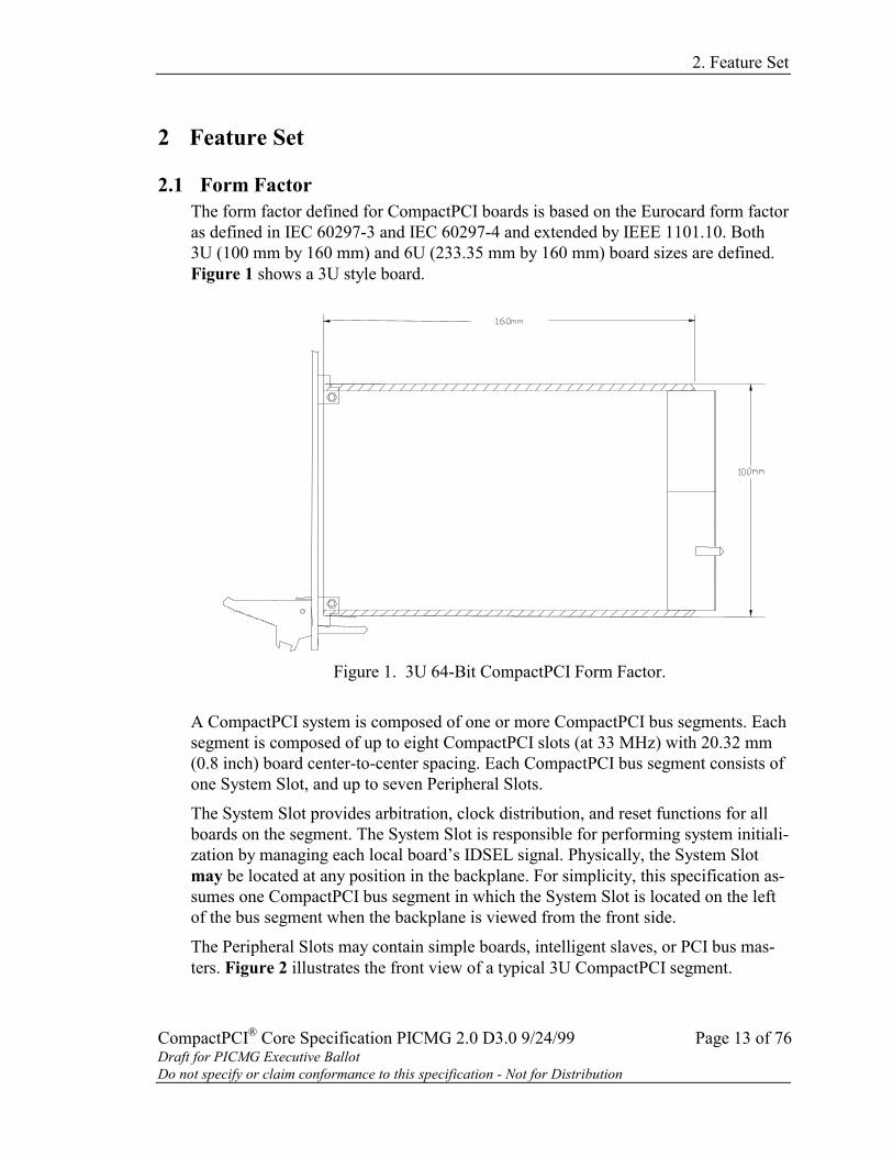
2.1 Form FactorThe form factor defined for CompactPCI boards is based on the Eurocard form factoras defined in IEC 60297-3 and IEC 60297-4 and extended by IEEE 1101.10. Both3U (100 mm by 160 mm) and 6U (233.35 mm by 160 mm) board sizes are defined.Figure 1 shows a 3U style board.
Figure 1. 3U 64-Bit CompactPCI Form Factor.
A CompactPCI system is composed of one or more CompactPCI bus segments. Eachsegment is composed of up to eight CompactPCI slots (at 33 MHz) with 20.32 mm(0.8 inch) board center-to-center spacing. Each CompactPCI bus segment consists ofone System Slot, and up to seven Peripheral Slots.
The System Slot provides arbitration, clock distribution, and reset functions for allboards on the segment. The System Slot is responsible for performing system initiali-zation by managing each local board’s IDSEL signal. Physically, the System Slotmay be located at any position in the backplane. For simplicity, this specification as-sumes one CompactPCI bus segment in which the System Slot is located on the leftof the bus segment when the backplane is viewed from the front side.
The Peripheral Slots may contain simple boards, intelligent slaves, or PCI bus mas-ters. Figure 2 illustrates the front view of a typical 3U CompactPCI segment.

2. Feature Set
Page 14 of 76 PICMG 2.0 D3.0 9/24/99Draft, Not for Distribution – Do Not Claim Conformance
Other topologies besides the linear arrangement illustrated in Figure 2 are allowedby CompactPCI. However, this specification and all backplane simulations have as-sumed a linear topology using 20.32 mm (0.8 inch) board center-to-center spacingwith the System Slot located on either end of the bus segment. Any other topologyshall be simulated or otherwise verified to ensure compliance to the PCIspecification.
= PERIPHERAL SLOT
1
3edcz a b f
1
12-P1
2
25
4 5
= SYSTEM SLOT22
2-P2
1
7-P1
76cz a b d e f
8
1
25
7-P222
Figure 2. 3U CompactPCI Backplane Example.
CompactPCI defines slot numbering based on the concept of physical and logicalslots. Physical slot numbers shall start at 1 in the top-left corner of the card cage. AllCompactPCI systems should label all physical slots within the compatibility glyphs.Figure 2 illustrates an example of physical slot numbering within the compatibilityglyphs (e.g., 1 ).
Logical slot numbers shall be defined by the IDSEL signal and associated addressused to select the slot. Logical numbers are used in the nomenclature to define thephysical outline of a connector on a bus segment. Logical numbers are illustrated inFigure 2 just below the connector outline (e.g., 2-P1). Logical and physical slotnumbers may not always coincide. In either case, Chapter 3 defines signal routingrequirements.
Capability glyphs provide visual indication of backplane connector and board capa-bility. Capability glyphs are:
• (triangle) for System Slot
• (circle) for Peripheral Slots
2. Feature Set
CompactPCI® Core Specification PICMG 2.0 D3.0 9/24/99 Page 15 of 76Draft for PICMG Executive BallotDo not specify or claim conformance to this specification - Not for Distribution
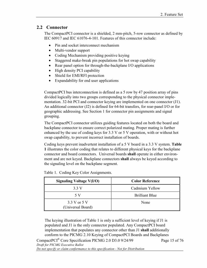
2.2 ConnectorThe CompactPCI connector is a shielded, 2 mm-pitch, 5-row connector as defined byIEC 60917 and IEC 61076-4-101. Features of this connector include:
• Pin and socket interconnect mechanism• Multi-vendor support• Coding Mechanism providing positive keying• Staggered make-break pin populations for hot swap capability• Rear panel option for through-the-backplane I/O applications• High density PCI capability• Shield for EMI/RFI protection• Expandability for end user applications
CompactPCI bus interconnection is defined as a 5 row by 47 position array of pinsdivided logically into two groups corresponding to the physical connector imple-mentation. 32-bit PCI and connector keying are implemented on one connector (J1).An additional connector (J2) is defined for 64-bit transfers, for rear-panel I/O or forgeographic addressing. See Section 1 for connector pin assignments and signalgrouping.
The CompactPCI connector utilizes guiding features located on both the board andbackplane connector to ensure correct polarized mating. Proper mating is furtherenhanced by the use of coding keys for 3.3 V or 5 V operation, with or without hotswap capability, to prevent incorrect installation of boards.
Coding keys prevent inadvertent installation of a 5 V board in a 3.3 V system. Table1 illustrates the color coding that relates to different physical keys for the backplaneconnector and board connectors. Universal boards shall operate in either environ-ment and are not keyed. Backplane connectors shall always be keyed according tothe signaling level on the backplane segment.
Table 1. Coding Key Color Assignments.
Signaling Voltage V(I/O) Color Reference
3.3 V Cadmium Yellow
5 V Brilliant Blue
3.3 V or 5 V(Universal Board)
None
The keying illustration of Table 1 is only a sufficient level of keying if J1 ispopulated and J1 is the only connector populated. Any CompactPCI boardimplementation that populates any connector other than J1 shall additionallyconform to the PICMG 2.10 Keying of CompactPCI Boards and Backplanes

2. Feature Set
Page 16 of 76 PICMG 2.0 D3.0 9/24/99Draft, Not for Distribution – Do Not Claim Conformance
specification. The color coded keying mechanism provided in the J1 connector issufficient keying only for 3U and 6U non-rear I/O 32 bit signaling boards, any otherimplementations shall conform to the keying mechanism specified in PICMG 2.10.
2.3 ModularityA key feature of CompactPCI is system modularity. Modularity is achieved by utiliz-ing various Eurocard form factors along with a versatile IEC-61076-4-101 connector.Either the 3U or 6U form factor, or a combination of the two, may be used directlyto create a system. The IEC-61076-4-101 connector is available in a variety of me-chanical form factors for different applications.
2.4 Hot Swap CapabilityThe PICMG 2.1, Hot Swap Specification shall be used as a reference for details onthe design issues regarding hot swap boards or systems.

3. Electrical Requirements
CompactPCI® Core Specification PICMG 2.0 D3.0 9/24/99 Page 17 of 76Draft for PICMG Executive BallotDo not specify or claim conformance to this specification - Not for Distribution
3 Electrical RequirementsThis section documents the electrical requirements for CompactPCI boards and back-planes.
3.1 Board Design RulesCompactPCI board design shall adhere to the design requirements for standard desk-top PCI boards as specified in the PCI Specification. This section documents addi-tional requirements or restrictions as needed. The design rules in sections 3.1through 3.4 apply to PCI bus operation up to 33 MHz. Refer to section 3.5 for rulesapplicable to 66 MHz designs.
3.1.1 Decoupling Requirements
Each CompactPCI board shall have adequate decoupling for its intendedapplication. Table 2 illustrates the minimum requirements that should be used.For CompactPCI Hot Swap boards, these requirements are modified. Refer tothe Hot Swap Specification, PICMG 2.1 for details.
Table 2. Board Decoupling Requirements.
Connector Mnemonic Description Decoupling Capacitance Voltage
.1 µF±20%(1)
10 µF±20%(2)
P1 5V +5 VDC 15 V min.
P1 3.3V +3.3 VDC 10 V min.
P1 V(I/O) +5/3.3 VDC 15 V min.
P1 +12V +12 VDC (3) 35 V min.
P1 -12V -12 VDC (3) 35 V min.
P2(4) V(I/O) +5/3.3 VDC 15 V min.Notes:
(1) For all voltages, one .1 µF ceramic capacitor suitable for high speed decoupling should beprovided close to the connector to decouple every 10 power pins. Note this rule applies toall power pins even if unused on board.
(2) One 10 µf low ESR capacitor per voltage should be located close to the connector (see note3).
(3) Only required if ±12 V is used on board. Note, one .1 µF capacitor should be provided on+12 V and –12 V even if unused on board.
(4) Requirements for P2 in a 64-bit system. If P2 is used for user defined I/O, additional de-coupling capacitance may be required.

3. Electrical Requirements
Page 18 of 76 PICMG 2.0 D3.0 9/24/99Draft, Not for Distribution – Do Not Claim Conformance
3.1.2 CompactPCI Signal AdditionsCompactPCI defines some additional signals beyond the PCI specification thatmay be applicable to board designs. Please refer to Section 3.2.7 for further de-scriptions.
3.1.3 CompactPCI Stub Termination
Many bussed PCI signals shall include a 10 Ω series stub termination resistor lo-cated on the board at the CompactPCI connector interface. The signals thatshall be terminated are: AD0-AD31, C/BE0#-C/BE3#, PAR, FRAME#,IRDY#, TRDY#, STOP#, LOCK#, IDSEL, DEVSEL#, PERR#, SERR#, andRST#.
Table 3. Stub Termination Resistor.
Parameter Min. Nominal Max. Units CommentRterm -5% 10 +5% Ohms Stub terminating resistor
located at connector onboard
If used by a board, the following signals shall also be terminated: INTA#,INTB#, INTC#, INTD#, AD32-AD63, C/BE4#-C/BE7#, REQ64#, ACK64#,and PAR64.
The following signals do not require a stub termination resistor: CLK, REQ#,and GNT#.
The stub termination minimizes the effect of the stub on each board to the PCIbackplane. The resistor shall be placed within 15.2 mm (0.6 inches) of the sig-nal’s connector pin. This length shall be included in the overall length of tracethat is allowed for the signal as described in Sections 3.1.4 and 3.1.6.
Peripheral boards that drive REQ# should provide a series terminating resistor(sized according to the output characteristics of the buffer) at the driver pin (nota stub termination resistor at the connector). On System Slot boards, a seriesresistor (sized according to the output characteristics of the clock buffer) shallbe located at the driver for the CLK signal provided to each slot. Each SystemSlot board’s GNT# signal shall also be series terminated at the driver with aresistor as required by the driving buffer output characteristics.
3.1.4 Peripheral Board Signal Stub Length
Signal length for 32-bit or 64-bit signals (J1, J2) shall be less than or equal to63.5 mm (2.5 inches). This length is measured from the connector pin through

3. Electrical Requirements
CompactPCI® Core Specification PICMG 2.0 D3.0 9/24/99 Page 19 of 76Draft for PICMG Executive BallotDo not specify or claim conformance to this specification - Not for Distribution
the stub or series termination resistor (described in Section 3.1.3) to the PCI de-vice pin. These lengths are more generous than the PCI Specification require-ments but also include the resistor in the total trace length.
A maximum of one PCI load shall be allowed on any PCI signal on anyperipheral board. Peripheral boards with more than one load are not compliantwith the CompactPCI Specification and shall not be declared CompactPCIcompatible.
3.1.5 Characteristic Impedance
Boards shall be fabricated to provide CompactPCI signal traces within thecharacteristic impedance range given in Table 4.
Table 4. Board Characteristics.
Parameter Min. Nominal Max. Units CommentZ0 -10% 65 +10% Ohms PCB traces only, but
including platedthrough-holes.
3.1.6 System Slot Board Signal Stub Length
The System Slot shall have signal lengths less than or equal to 63.5 mm (2.5inches) for 32-bit or 64-bit boards.
The System Slot may have two PCI loads on each signal on a PCI backplanesegment to accommodate practical implementations of PCI-based CPU designs.If an additional load is added on the System Slot board, only one stub termina-tion resistor per PCI signal shall be required as defined in Section 3.1.3.
On the system slot, when two PCI loads are used, the signal shall be routedlinearly from the connector, to the first load and then to the second load. Thestub connecting to the first load shall be less than 0.5inch.
3.1.7 Peripheral Board PCI Clock Signal Length
On Peripheral boards, the PCI clock signal length shall be 63.5 mm ± 2.54 mm(2.5 inches ±0.1 inches), and shall drive only one load on the board.
3.1.8 Pull-Up Location
Pull-up resistors required by the PCI specification shall be located on the SystemSlot board. Table 5 provides values for both 5 V and 3.3 V signalingenvironments. All values assume nine loads (two on the System Slot board plusone each on seven other boards) and ± 5% resistor values. The pull-up resistor,for those signals requiring a pull-up, shall be placed on the in-board side of the

3. Electrical Requirements
Page 20 of 76 PICMG 2.0 D3.0 9/24/99Draft, Not for Distribution – Do Not Claim Conformance
stub termination resistor. The stub length for the pull-up resistor shall be lessthan 0.5inch, with the stub length being considered as a part of the total tracelength.
A System Slot board that supports both signaling modes shall be designed tosupport the appropriate pull-up value for the signaling environment that it isoperating in. A board that may function as either a System Slot board orPeripheral board shall not have the pull-up resistors connected when inPeripheral board function.
Table 5. Pull-up Resistor Values.
Signaling Voltage Min. Nominal Max. Units
5 V -5% 1.0 +5% KΩ3.3 V -5% 2.7 +5% KΩ
In addition to the pull-ups required on control signals, ALL System Slot boardsshall provide pull-up resistors for the 64-bit data path expansion signals,AD[63::32], C/BE[7::4]#, and PAR64.
The System Slot board shall provide a pull-up resistor for the REQ64# andACK64# signals even if the System Slot board does not use these signals, as inthe case of a 32-bit System Slot board. The above requirements accommodate64-bit peripheral boards used in platforms with 32-bit or 64-bit System SlotBoards. The pull-up resistor also prevents floating REQ64# or ACK64# signalson 64-bit boards. Refer to section 3.4 for additional details on 64-bit signaling.
Each peripheral board using GNT# shall have a 100 KΩ pull-up resistor toprevent a floating input if GNT# is not being driven by the System Slot boarddesigned prior to the 3.0 revision of this specification.
See also Sections 3.2.7.4 and 3.2.7.5 for details of pull-up for Legacy IDEInterrupt and System Enumeration related signals.
3.1.9 Board Connector Shield Requirements
The J1 and J2 connectors shall load a shield at row F on the board. This shieldprovides a low impedance return path for logic ground between the board andthe CompactPCI backplane. Boards that do not use this shield are not compliantand are not guaranteed to work in all CompactPCI system topologies.
The Z row shield option that is provided for in the IEC-61076 connector is notrequired for CompactPCI boards and shall not be loaded if it protrudes into theinterboard separation plane.

3. Electrical Requirements
CompactPCI® Core Specification PICMG 2.0 D3.0 9/24/99 Page 21 of 76Draft for PICMG Executive BallotDo not specify or claim conformance to this specification - Not for Distribution
3.2 Backplane Design RulesCompactPCI defines a backplane environment that may have up to eight slots at33MHz. 66Mhz backplanes may have up to five slots. See Section 3.5.3 for 66Mhzdesign rules.
One slot, the System Slot, provides the clocking, arbitration, configuration, and inter-rupt processing for the other seven slots. Fewer slots may be provided in a Com-pactPCI backplane, but the following sections assume that a maximum configurationis employed in a linear topology using 20.32 mm (0.8 inch) board center-to-centerspacing with the System Slot located on either end of the bus segment. Any other to-pology shall be simulated or otherwise verified to ensure compliance to the PCIspecification.
It is possible to design a backplane capable of both 33Mhz and 66Mhz operation. SeeSection 3.5.3 for 66Mhz design rules. M66EN shall be grounded on all slots forbackplanes with more than five slots.
Backplanes shall provide separate power planes for 3.3 V, 5 V, and ground. IfV(I/O) is configurable as 3.3 V or 5 V, then a separate power plane shall be dedi-cated for V(I/O).
3.2.1 Characteristic Impedance
Backplanes shall be fabricated to provide CompactPCI signal traces within thecharacteristic impedance range given in Table 6.
Table 6. Backplane Characteristics.
Parameter Min. Nominal Max. Units CommentZ0 -10% 65 +10% ohms PCB without connectors
or boards installed, butincluding platedthrough-holes
3.2.2 Eight-Slot Backplane TerminationSystem simulation has shown that when using the strongest PCI buffer allowed(refer to the PCI specification V-I curves) and with a lightly loaded eight-slotbackplane configuration with the System Slot and its adjacent Peripheral Slotloaded (only two boards), that the 10 ns maximum propagation delay for PCIsignals is violated.
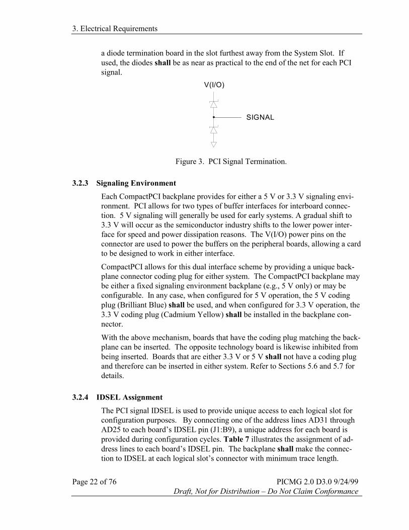
For this specific system configuration, fast Schottky diode signal termination(For example: see Texas Instruments 74S1053 diode array) shall be added to theend of the backplane furthest from the System Slot on all bused PCI signals, asillustrated in Figure 3. The diodes may be added directly to the backplane or via
3. Electrical Requirements
Page 22 of 76 PICMG 2.0 D3.0 9/24/99Draft, Not for Distribution – Do Not Claim Conformance
a diode termination board in the slot furthest away from the System Slot. Ifused, the diodes shall be as near as practical to the end of the net for each PCIsignal.
V(I/O)
SIGNAL
Figure 3. PCI Signal Termination.
3.2.3 Signaling EnvironmentEach CompactPCI backplane provides for either a 5 V or 3.3 V signaling envi-ronment. PCI allows for two types of buffer interfaces for interboard connec-tion. 5 V signaling will generally be used for early systems. A gradual shift to3.3 V will occur as the semiconductor industry shifts to the lower power inter-face for speed and power dissipation reasons. The V(I/O) power pins on theconnector are used to power the buffers on the peripheral boards, allowing a cardto be designed to work in either interface.
CompactPCI allows for this dual interface scheme by providing a unique back-plane connector coding plug for either system. The CompactPCI backplane maybe either a fixed signaling environment backplane (e.g., 5 V only) or may beconfigurable. In any case, when configured for 5 V operation, the 5 V codingplug (Brilliant Blue) shall be used, and when configured for 3.3 V operation, the3.3 V coding plug (Cadmium Yellow) shall be installed in the backplane con-nector.
With the above mechanism, boards that have the coding plug matching the back-plane can be inserted. The opposite technology board is likewise inhibited frombeing inserted. Boards that are either 3.3 V or 5 V shall not have a coding plugand therefore can be inserted in either system. Refer to Sections 5.6 and 5.7 fordetails.
3.2.4 IDSEL AssignmentThe PCI signal IDSEL is used to provide unique access to each logical slot forconfiguration purposes. By connecting one of the address lines AD31 throughAD25 to each board’s IDSEL pin (J1:B9), a unique address for each board isprovided during configuration cycles. Table 7 illustrates the assignment of ad-dress lines to each board’s IDSEL pin. The backplane shall make the connec-tion to IDSEL at each logical slot’s connector with minimum trace length.

3. Electrical Requirements
CompactPCI® Core Specification PICMG 2.0 D3.0 9/24/99 Page 23 of 76Draft for PICMG Executive BallotDo not specify or claim conformance to this specification - Not for Distribution
One additional PCI device on the CompactPCI bus segment is allowed on theSystem Slot board. This device may be selected using lower ADxx lines in therange of AD11 to AD24.
3.2.5 REQ#/GNT# AssignmentThe System Slot interfaces to seven pairs of REQx#/GNTx# pins called REQ0#-REQ6# and GNT0#-GNT6#. Each Peripheral Board interfaces to one pair ofREQx#/GNTx# signals using pins called REQ# (J1:A6) and GNT# (J1:E5).Table 7 lists the assignment of request/grant signals to each board’s REQ# andGNT# pins.
The System Slot on any given CompactPCI backplane segment shall support thefull complement of REQ#/GNT# signals.
The System Slot board shall support seven pairs of REQx#/GNTx# signals.
Table 7. System to Logical Slot Signal Assignments.
Signal Connector:Pin Signal Connector:PinSystem Slot ( ), Logical Slot 1 Peripheral Slot ( ), Logical Slot 2AD31 P1:E6 IDSEL(1) P1:B9
REQ0# P1:A6 REQ# P1:A6GNT0# P1:E5 GNT# P1:E5System Slot ( ), Logical Slot 1 Peripheral Slot ( ), Logical Slot 3AD30 P1:A7 IDSEL(1) P1:B9
REQ1# P2:C1 REQ# P1:A6GNT1# P2:D1 GNT# P1:E5System Slot ( ), Logical Slot 1 Peripheral Slot ( ), Logical Slot 4AD29 P1:B7 IDSEL(1) P1:B9
REQ2# P2:E1 REQ# P1:A6GNT2# P2:D2 GNT# P1:E5System Slot ( ), Logical Slot 1 Peripheral Slot ( ), Logical Slot 5AD28 P1:C7 IDSEL(1) P1:B9
REQ3# P2:E2 REQ# P1:A6GNT3# P2:C3 GNT# P1:E5System Slot ( ), Logical Slot 1 Peripheral Slot ( ), Logical Slot 6AD27 P1:E7 IDSEL(1) P1:B9
REQ4# P2:D3 REQ# P1:A6GNT4# P2:E3 GNT# P1:E5System Slot ( ), Logical Slot 1 Peripheral Slot ( ), Logical Slot 7AD26 P1:A8 IDSEL(1) P1:B9
REQ5# P2:D15 REQ# P1:A6GNT5# P2:E15 GNT# P1:E5System Slot ( ), Logical Slot 1 Peripheral Slot ( ), Logical Slot 8AD25 P1:D8 IDSEL(1) P1:B9
REQ6# P2:D17 REQ# P1:A6GNT6# P2:E17 GNT# P1:E5
Notes:

3. Electrical Requirements
Page 24 of 76 PICMG 2.0 D3.0 9/24/99Draft, Not for Distribution – Do Not Claim Conformance
(2) (1) The IDSEL signal at each slot shall be connected with minimal trace length atthe slot that is intended. For example, at logical slot 6, IDSEL shall be connected toAD27 with minimal trace length.
3.2.6 PCI Interrupt Binding
Interrupt binding of the BIOS setup program shall require backplane assign-ments from the System Slot interrupt pins INTA#-INTD# to the logical boardslot interrupts as defined in Table 8.
Backplane assignments rotate through logical board slots to provide a uniquePCI interrupt to each board for the first four PCI connectors (assuming that eachboard drives just its INTA# signal). Rotating interrupt assignments allows multi-ple PCI peripherals that drive only INTA# in order to utilize a different interrupton the System Slot board without the need to share an interrupt with another PCIinterface. Since multi-function PCI devices are allowed to drive more than oneinterrupt, shared interrupts may be required even within the first four board slots.In addition, the rotating pattern repeats itself after logical slot four, which alsorequires the sharing of an interrupt for slots that are four connectors apart (logi-cal slots 2 and 6 for example).
The Interrupt assignments are consistent with the PCI-PCI Bridge Specificationas defined by the PCI SIG. This is to allow PCI-PCI bridge technology on CPUboards between Bus 0 and CompactPCI.
Although PCI software device drivers are designed to allow sharing of interruptsignals, sharing an interrupt with another device can affect interrupt latency andis generally avoided where possible.
Please see Section 3.2.7.4 for interrupt support for legacy IDE devices.
Table 8. System to Logical Slot Interrupt Assignments.
Slot 8 (IDSEL=AD25)Slot 4 (IDSEL=AD29)Slot 3 (IDSEL=AD30)Slot 2 (IDSEL=AD31)Slot 1 (System Slot)
(A3) (A3)
(B3)
(C3)
(E3)
(A3)(A3)INTA#(A3)
INTD#(E3)
INTB#(B3)
INTC#(C3)
(E3)(E3)(E3)
System Slot INTC# net
System Slot INTD# net
System Slot INTB# net
System Slot INTA# net
(B3)
(C3)
(B3)
(C3)
(B3)
(C3)

3. Electrical Requirements
CompactPCI® Core Specification PICMG 2.0 D3.0 9/24/99 Page 25 of 76Draft for PICMG Executive BallotDo not specify or claim conformance to this specification - Not for Distribution
3.2.7 CompactPCI Signal AdditionsCompactPCI utilizes PCI signals as defined by the PCI Local Bus Specificationwith some additional signals. These additional signals do not affect the PCI sig-nals but may enhance system operation by providing push button reset, powersupply status, System Slot identification, geographic addressing, systemmanagement, and legacy IDE interrupt support features.
3.2.7.1 Push Button Reset (PRST#)PRST# may be used in a CompactPCI system to reset the System Slotboard, which in turn would reset the rest of the system using the PCI RST#signal. PRST# is an active low true TTL signal generated by a switch clo-sure or an open-collector driver. It is the responsibility of the System Slotboard receiving PRST# to debounce it as required. The System Slot boardshall terminate PRST# with a minimum 1KΩ pullup resistor to V(I/O).
3.2.7.2 Power Supply Status (DEG#, FAL#)Power sub-system status may be determined from two low true TTL powersupply status signals available on backplanes utilizing modular power sup-plies implementing the optional DEG# and FAL# signals. The System Slotboard shall terminate both signals with a minimum 1KΩ pullup resistor toV(I/O), even if the system board does not use these signals. Please seeSection 3.2.8.2 for more information.
3.2.7.3 System Slot Identification (SYSEN#)This pin is grounded on the CompactPCI backplane segment at the SystemSlot so the board may identify installation into the System Slot. This pin isnot connected on the backplane for the remaining slots. Boards that sensethis signal shall provide their own pull-up to V(I/O) and disable all SystemSlot functions, such as clock generation and bus arbitration when it is not in-stalled in a System Slot.
3.2.7.4 Legacy IDE Interrupt SupportTwo additional non-PCI interrupts, INTP and INTS, are defined for boardsusing legacy interrupts. Support of these interrupts is optional. INTP (pinD4) is used as a steerable interrupt which may be routed to any legacy ISAinterrupt on the system master. The system master shall provide a way forthe user to control the usage and routing of this interrupt, e.g. via the BIOSsetup menu. After PCI Reset, this steerable interrupt shall be disabled on thesystem master and any peripheral board supporting this interrupt.
On legacy system masters, INTP may be hardwired to a single legacy ISAinterrupt. This especially includes the option to use INTP as legacy IDEinterrupt as proposed by former revisions of this specification.
INTP is an active high TTL signal and does not have the requirement ofmeeting the PCI electrical buffer characteristics. The System Slot board

3. Electrical Requirements
Page 26 of 76 PICMG 2.0 D3.0 9/24/99Draft, Not for Distribution – Do Not Claim Conformance
shall provide a 1KΩ pullup to V(I/O), even if the System Slot board doesnot support this signal.
INTS (pin E4) may be used as serialized interrupt in compliance with the”Serialized IRQ Support for PCI Systems” specification, Rev. 6.0,September 1995.
The system master shall provide a way for the user to control the usage androuting of this interrupt, e.g. via the BIOS setup menu. After PCI Reset, thisserialized interrupt shall be disabled on the system master and anyperipheral boards supporting the serialized IRQ protocol.
INTS is synchronous to the PCI clock and has the requirement of meetingthe PCI electrical buffer characteristics. This line shall have a pull upresistor on the system slot board in accordance with Section 3.1.8 and atermination resistor in accordance with Section 3.1.3 on any boardsupporting this signal. The electrical characteristics and routing of the PCBtrace shall comply with sections 3.1.4 through 3.1.7.
The support for INTP and INTS shall be clearly documented by the systemslot and peripheral board vendors.
3.2.7.5 System Enumeration (ENUM#)This low true TTL open-collector signal shall be driven by hot swap com-patible boards after insertion and prior to removal. The System Master usesthis interrupt signal to force software to interrogate all boards within thesystem for resource allocation regarding I/O, memory, and interrupt usage.The System Slot board shall terminate ENUM# with a pullup resistor as de-fined in Section 3.1.8. Different levels of hot swap capability are defined inthe CompactPCI Hot Swap Specification regarding the ENUM# Signal.Consult the CompactPCI Hot Swap Specification for further details.
3.2.7.6 Geographic Addressing (GA[4..0])For backplanes, if P2 is populated on a particular slot, then it shall supportthe GA[4..0] geographic addressing signals for unique slot identification.Boards that use geographical address signals GA[4..0] shall be pulled upwith a 10.0 KΩ ±10% resistor.
For backplanes the physical slot address (GA[4..0]) shall be encoded on thebackplane by grounding and leaving unconnected different combinations ofpins at each connector. Physical slot addresses are defined by the physicalslot number in Section 2.1. Table 9 illustrates the physical slot number andits physical slot address defined by GA[4..0]. Physical slot “0” is reservedfor future use. Geographical address “31” is the default address that resultswhen a geographical address capable board is installed in a backplane slotthat does not support geographical addressing.

3. Electrical Requirements
CompactPCI® Core Specification PICMG 2.0 D3.0 9/24/99 Page 27 of 76Draft for PICMG Executive BallotDo not specify or claim conformance to this specification - Not for Distribution
Boards that support system management may use these signals to provide aunique address within the system. Refer to the pending CompactPCI SystemManagement Specification for further information
Table 9. Physical Slot Addresses.
Physical SlotNumber
GA[4](J2-A22)
GA[3](J2-B22)
GA[2](J2-C22)
GA[1](J2-D22)
GA[0](J2-E22)
0(1) GND GND GND GND GND1 GND GND GND GND Open2 GND GND GND Open GND3 GND GND GND Open Open4 GND GND Open GND GND5 GND GND Open GND Open6 GND GND Open Open GND7 GND GND Open Open Open8 GND Open GND GND GND9 GND Open GND GND Open10 GND Open GND Open GND11 GND Open GND Open Open12 GND Open Open GND GND13 GND Open Open GND Open14 GND Open Open Open GND15 GND Open Open Open Open16 Open GND GND GND GND17 Open GND GND GND Open18 Open GND GND Open GND19 Open GND GND Open Open20 Open GND Open GND GND21 Open GND Open GND Open22 Open GND Open Open GND23 Open GND Open Open Open24 Open Open GND GND GND25 Open Open GND GND Open26 Open Open GND Open GND27 Open Open GND Open Open28 Open Open Open GND GND29 Open Open Open GND Open30 Open Open Open Open GND31 Open Open Open Open Open
Note:

3. Electrical Requirements
Page 28 of 76 PICMG 2.0 D3.0 9/24/99Draft, Not for Distribution – Do Not Claim Conformance
(1) Physical slot number “0” is reserved for future use.
3.2.7.7 System management busThree pins, (IPMB_SCL, IPMB_SDA, IPMB_PWR), are defined on J1/P1for incorporating system management features including boardidentification, environmental and voltage monitoring, etc.
Three pins, (ICMB_SCL, ICMB_SDA, ICMB_PWR), are reserved on J2/P2for possible use by non-backplane bussed system management functions.
Refer to the PICMG 2.9, CompactPCI System Management Specificationfor further information.
The IPMB_PWR backplane traces shall have a current carrying capacity ofat least 100 mA per slot.
3.2.8 Power DistributionPower is distributed in a CompactPCI system by utilizing a backplane. Eachbackplane shall make provisions for the standard regulated direct current (DC)supply voltages in Table 10 below.
Table 10. Power Specifications.
Mnemonic Description Nominal Value Tolerance(2) Max. Ripple(p-p)(3)
5 V +5 VDC 5.0 V +5%/-3% 50 mV(1)(4)
3.3 V +3.3 VDC 3.3 V +5%/-3% 50 mV(1)(4)
+12 V +12 VDC 12.0 V ±5% 240 mV(1)(5)
-12 V -12 VDC -12.0 V ±5% 240 mV(1)(5)
V(I/O) PCI I/OBuffer
Voltage
5.0V or 3.3V +5%/-3% 50mV(1)(4)
GND GroundNote:
(1) Maximum ripple is very difficult to accurately measure and therefore requires goodmeasurement techniques. Measurement should be made at 20 MHz bandwidth with aminimum length ground strap. Each CompactPCI slot must meet this specification.
(2) This specification is for power delivered to each slot and it includes both the powersupply and the backplane tolerance.
(3) For ripple directly related to the line frequency, the maximum ripple shall be a maximum10mV(p-p) for +12V and -12V and 5mV(p-p) for +5V and +3.3V
3. Electrical Requirements
CompactPCI® Core Specification PICMG 2.0 D3.0 9/24/99 Page 29 of 76Draft for PICMG Executive BallotDo not specify or claim conformance to this specification - Not for Distribution
(4) Distribution between board and backplane: 20 mV for backplane; 30mV for board.
(5) Distribution between board and backplane: 96 mV for backplane; 144 mV for board.

3. Electrical Requirements
Page 30 of 76 PICMG 2.0 D3.0 9/24/99Draft, Not for Distribution – Do Not Claim Conformance
3.2.8.1 External Power ConnectionsPower terminals may be located on the front or rear side of the backplanefor external power sources. Several styles of high current printed circuitboard terminals are available. At least one per supply voltage shall beprovided.
3.2.8.2 In-Rack Power ConnectionsThe PICMG 2.11 Power Interface Specification defines several methods forimplementing In-rack modular power supplies. Previous versions of thecore specification (PICMG 2.0) have referenced an IEC 603-2 (DIN 41612)style connector for modular power supplies, which is one of the referencedconfigurations in PICMG 2.11. For further details refer to PICMG 2.11Power Interface Specification.
3.2.8.3 V(I/O) Current Carrying CapabilityBackplanes shall be designed to provide an aggregate 4A minimum to eachCompactPCI slot through that slot's V(I/O) pins. Boards may assume thatup to 4A of current (at either 5V or 3.3V) is available through the V(I/O)pins at the connector. This requirement merely grants permission for boardsto draw power from V(I/O) in addition to 5V and 3.3V power pins. Overallsystem power allocation is a system integration concern.
3.2.9 Power Decoupling
CompactPCI boards may utilize any of the voltages in Table 10. Without ade-quate power decoupling on the backplane for the 5 V and 3.3 V power, intermit-tent operation may result. The backplane has dedicated 5 V and 3.3 V powerpins along with V(I/O) power pins. The V(I/O) power pins are connected to ei-ther 5 V or 3.3 V depending on if 5 V or 3.3 V backplane signals are being used.See Section 5.6.
All power voltages shall be decoupled to ground in such a manner as to providefor reasonable management of switching currents (di/dt). Low impedance powerplanes and connections to low equivalent series resistance (ESR) capacitorsshould be used. Even if a system does not use 3.3 or 5 V, the unused power pinsshall be connected and decoupled to provide an additional AC return path.Table 11 illustrates the bypass guidelines that shall, at a minimum, be used foreach connector.

3. Electrical Requirements
CompactPCI® Core Specification PICMG 2.0 D3.0 9/24/99 Page 31 of 76Draft for PICMG Executive BallotDo not specify or claim conformance to this specification - Not for Distribution
Table 11. Backplane Decoupling Recommendations.
Mnemonic Description Decoupling Capacitance Voltage
5V +5 VDC 44 µF ± 20% (1) 15 V min.
3.3V +3.3 VDC 44 µF ± 20% (1) 10 V min.
V(I/O) +5/3.3 VDC 44 µF ± 20% (1) 15 V min.
+12V +12 VDC 15 µF ± 20% 35 V min.
-12V -12 VDC 15 µF ± 20% 35 V min.Note:
(1) Recommended decoupling capacitance per connector best distributed across the lengthof each connector.
3.2.10 Healthy (Healthy#)
This pin is reserved for use in hot swap systems. The backplane SHALL leaveHEALTHY# open (not connected). This pin SHALL be bypassed on thebackplane at each slot with a 0.01uF capacitor to maintain the AC shieldingcapability of the line. Additional requirements may apply to some Hot Swapplatforms, refer to PICMG 2.1 for details.
3.3 33 MHz PCI Clock DistributionThe System Slot board shall provide clock signals for all PCI peripherals in the sys-tem, including devices on the System Slot board. Peripheral boards are providedclock signals via the CompactPCI backplane. A maximum skew of 2 ns shall bemaintained across the system operating at 33 MHz between any two PCI devices atthe clock input of the integrated circuits.
Clock skew is the difference between the maximum and minimum propagation delayof any PCI clock signal. There are two components that contribute to clock skew in aCompactPCI system:
1. Backplane Clock Skew. The CompactPCI backplane provides the distribution ofclock signals for all of the board slots in the system. The differences in the tracerouting and net topologies contribute to skew and also define the longest clockdelay that shall be considered in the design of the system and still meet overallsystem clock skew requirements.
2. System Slot Board Clock Skew. This is the clock skew that may be attributed tothe onboard routing differences (if any) of all of the PCI clocks as well as theskew specification for the type of integrated circuit driver used for clock distribu-

3. Electrical Requirements
Page 32 of 76 PICMG 2.0 D3.0 9/24/99Draft, Not for Distribution – Do Not Claim Conformance
tion. The onboard clock routing shall be designed to complement the propagationdelays of distributing the clock to a backplane and still meet overall system skewrequirements.
3.3.1 Backplane Clock Routing Design Rules
CompactPCI backplanes shall be designed to provide a consistent environmentfor System Slot boards with regard to backplane clock routing. Design rules as-sume a linear backplane with the System Slot at one end of the bus segment and20.32 mm (0.8 inch) connector spacing.
The System Slot provides 7 clock signals, which dedicates a unique clock toeach slot. Correspondence between individual clock signals and physical slots isarbitrary.
Backplanes shall use these clock lines to provide a single clock line per slot.Clock lines shall not be shared. These clock lines shall be routed between 135mm (5.3 inches) and 185 mm (7.3 inches) in length.
System Slot boards shall drive each of the 7 clock lines.
3.3.2 System Slot Board Clock Routing Design Rules
The System Slot clock distribution circuitry shall be designed to accommodateup to 1.2 ns of backplane skew (minimum vs. maximum number of slots andvarious loading configurations). The following design rules apply to clock distri-bution to backplane peripherals and local (onboard) PCI peripherals. See Section3.1.3 for details of termination on System Slot Boards.
3.3.2.1 Clock Routing to Connector Clock PinsThe clock distribution circuitry on the System Slot shall provide a discreteclock signal to each of the CompactPCI connector pins defined as a PCIclock (CLK0, CLK1, CLK2, CLK3, CLK4, CLK5, CLK6). The routing ofthese signals shall be matched in length.
3.3.2.2 Clock Routing to Local PCI PeripheralsAny onboard PCI peripherals connected to the CompactPCI bus, includingPCI to PCI bridges, shall be provided a clock that is delayed toaccommodate the maximum propagation delay of the backplane clocks andstill meet the 2 ns overall skew requirement of the PCI Specification. Up to800 ps of skew is allowed for onboard clock distribution (including theclock buffer internal skew). The onboard clock signals shall be delayed be-yond the clocks routed to the backplane (Section 3.3.2.1) to accommodatebest and worst case backplane delays and the 63.5mm wire delay on theperipheral board.

3. Electrical Requirements
CompactPCI® Core Specification PICMG 2.0 D3.0 9/24/99 Page 33 of 76Draft for PICMG Executive BallotDo not specify or claim conformance to this specification - Not for Distribution
3.4 64-Bit Design Rules64-bit Peripheral boards must be configured correctly for the type of backplaneenvironment that they are plugged into. This includes 64-bit Peripheral boardsplugged into a system controlled by a 32-bit System Master as well as a 64-bitPeripheral board being plugged into a hot swap capable system. This revision of theCompactPCI specification differs from the PCI specification in the method that aPeripheral board determines the proper mode of operation.
The PCI Specification requires the following: On a 64-bit Peripheral board (32-bitPeripheral boards ignore REQ64#) REQ64# is sampled by the peripheral PCI deviceat the rising (trailing) edge of RST# to configure the upper 32-bit signal buffers forthe type of system that the peripheral is installed into. If REQ64# is high, the 64-bitdevice is allowed to drive the upper 32-bits signals active to prevent these signalsfrom floating. If REQ64# is sampled low, the device must configure the upper 32-bit signals for proper 64-bit operation.
CASE A: In CompactPCI, it is possible to have a 64-bit System Slot board pluggedinto a 32-bit only backplane, in which case it is required that any 64-bit Peripheralboards terminate the upper 32-bit signals for non 64-bit operation.
CASE B: It is also desirable to allow 64-bit Peripheral boards to communicate witheach other at 64-bits when in a 64-bit backplane controlled by a 32-bit System Slotboard. It is also desirable to allow the backplane to contain a mix of 32-bit and 64-bitslots.
CASE C: In a hot swap system, a board must configure itself because the time for asystem reset has long passed and the board is being installed in an operatingbackplane environment with PCI transactions occurring.
To allow boards to self configure for 64-bit operation, pin B5 of P2 is defined as64EN# and is GROUND in 64-bit backplanes and is left unconnected in 32-bitbackplanes. This signal is then used by onboard circuitry to self-configure duringRST#.
64EN# may be used in different ways to configure the local device. These include,but are not limited to, the following implementations:
a) Using 64EN# to drive the devices REQ64# signal during local reset bydecoupling the backplane REQ64# from the device during reset. After reset,the backplane REQ64# is then connected to the device for normal 64-bithandshake operation. In all cases, normal electrical operation of REQ64# shallbe maintained after reset. See Figure 4 below for an example of a possiblecircuit topology.
b) A 64-bit device may directly sample 64EN# during local reset to configure for32- or 64-bit operation.

3. Electrical Requirements
Page 34 of 76 PICMG 2.0 D3.0 9/24/99Draft, Not for Distribution – Do Not Claim Conformance
c) 64EN# may be used as part of an EEPROM serial pre-load mechanism toconfigure a 64-bit device for proper operation.
64-bit Peripheral boards shall use 64EN# to self-configure. Using the state ofREQ64# at the trailing edge of RST# is no longer allowed. With the requirementsgiven in this revision of the CompactPCI Specification, 64-bit capability is no longeran overall platform attribute. 64-bit capability can be determined on a slot by slotbasis.
The following circuit topology shows a FET in series with the backplane REQ64#and the devices REQ64# pin. During reset, the FET is OFF, and the resistance to the64EN# pin configures the device at the rising edge of reset. When RST# is de-asserted, the FET is enabled and REQ64# is allowed to function in it’s normal mode(As defined in PCI Specification 2.1).
64EN#
REQ64# FET
PCI DEVICE50KΩ
1KΩ
VIO
REQ64#
RST#LOCAL RST#
Figure 4. Local 64 Bit Initialization
To allow for the addition of the REQ64# series FET, the FET must not exceed thefollowing parameters:
ON resistance: 5-10Ω typical
The capacitance of the FET circuit must be isolated from ground. One method ofaccomplishing isolation of the FET capacitance is to use a discrete 3-Terminal FET,with the device's gate driven through a high valued resistor.
The FET may replace the 10Ω CompactPCI stub isolation resistor, but the circuittopology must provide the equivalent stub isolation of a non-FET implementation. Referto the CompactPCI Hot Swap Specification (PCIMG 2.1 R1.0) for details of the hot swapcircuit analysis.
3. Electrical Requirements
CompactPCI® Core Specification PICMG 2.0 D3.0 9/24/99 Page 35 of 76Draft for PICMG Executive BallotDo not specify or claim conformance to this specification - Not for Distribution
3.5 66 MHz Electrical RequirementsThis section documents the additional requirements for 66 MHz operation. 33 MHzdesign rules apply for features not specifically called out in this section.
3.5.1 66 MHz Board Design Rules
On 66 MHz Peripheral boards, the PCI clock signal length shall be 63.5 mm ±1mm (2.5 inches ±0.04 inches), and shall drive only one load on the board. Innerlayer stripline construction shall be used for all clock lines in order to equalizedelays.
3.5.2 66 MHz System Board Design Rules
On 66MHz System Slot Boards only one PCI load shall be allowed.
3.5.3 66MHz Backplane Design Rules
66 MHz CompactPCI defines a backplane environment that may have up to fiveslots.
One slot, the System Slot, provides the clocking, arbitration, configuration, andinterrupt processing for the other four slots. Fewer slots may be provided in aCompactPCI backplane, but the following sections assume that a maximumconfiguration is employed in a linear topology using 20.32 mm (0.8 inch) boardcenter-to-center spacing with the System Slot located on either end of the bussegment. Any other topology shall be simulated or otherwise verified to ensurecompliance to the PCI specification.
M66EN, the 66Mhz Enabling Line, shall be bussed to all slots in 66Mhzbackplanes.
Backplanes shall provide separate power planes for 3.3 V, 5 V, and ground.V(I/O) shall always be configured as 3.3V.
3.5.4 66MHz PCI Clock Distribution
The System Slot board shall provide clock signals for all PCI peripherals in the sys-tem, including the device on the System Slot board. Peripheral boards are providedclock signals via the CompactPCI backplane. A maximum skew of 1 ns shall bemaintained across the system operating at 66 MHz between any two PCI devices atthe clock input of the integrated circuits.
Clock skew is the difference between the maximum and minimum propagation delayof any PCI clock signal. There are two components that contribute to clock skew in aCompactPCI system:
1. Backplane Clock Skew. The CompactPCI backplane provides the distribution ofclock signals for all of the board slots in the system. The slight differences in the
3. Electrical Requirements
Page 36 of 76 PICMG 2.0 D3.0 9/24/99Draft, Not for Distribution – Do Not Claim Conformance
trace routing and net topologies contribute to skew and also define the longestclock delay that shall be considered in the design of the system and still meetoverall system clock skew requirements.
2. System Slot Board Clock Skew. This is the clock skew that may be attributed tothe onboard routing differences (if any) of all of the PCI clocks as well as theskew specification for the type of integrated circuit driver used for clock distribu-tion. The onboard clock routing shall be designed to complement the propagationdelays of distributing the clock to a backplane and still meet overall system skewrequirements. A System Slot board designed for both 33 MHz and 66 MHzoperation shall be designed with consideration for the different clockenvironments that it may operate in.
3.5.4.1 66 MHz backplane clock routing design rules66 MHz systems require only 4 Peripheral Slot clocks to be connected.Correspondence between individual clock signals and physical slots isarbitrary.
Backplanes shall use these clock lines to provide a single clock line per slot.Clock lines shall not be shared. These clock lines shall be routed to 160mm±1mm (6.300 inches ± 0.04) in length.
Inner layer stripline construction shall be used for all clock lines in order toequalize delays. Vias shall not be used to route any backplane clock lines.
3.5.5 66 MHz System Slot Board Clock Routing Design Rules
The System Slot clock distribution circuitry shall be designed to accommodateup to 200 ps of backplane and peripheral board skew. The following design rulesapply to clock distribution to backplane peripherals and local (onboard) PCIperipherals.
3.5.5.1 Clock Routing to Connector Clock PinsThe clock distribution circuitry on the System Slot shall provide a discreteclock signal to each of the CompactPCI connector pins defined as a PCIclock (CLK0, CLK1, CLK2, CLK3, CLK4, CLK5, and CLK6). The routingof these signals shall be matched in length.
3.5.5.2 Clock Routing to Local PCI PeripheralsAny onboard PCI peripherals connected to the CompactPCI bus, includingPCI to PCI bridges, shall be provided a clock that is delayed toaccommodate the maximum propagation delay of the backplane clocks andstill meet the 1 ns overall skew requirement. Up to 800 ps of skew isallowed for onboard clock distribution (including the clock buffer internalskew). The onboard clock signals shall be delayed beyond the clocks routed

3. Electrical Requirements
CompactPCI® Core Specification PICMG 2.0 D3.0 9/24/99 Page 37 of 76Draft for PICMG Executive BallotDo not specify or claim conformance to this specification - Not for Distribution
to the backplane (Section 3.5.5.1) to accommodate best and worst casebackplane delays and the 63.5mm wire delay on the peripheral board.
3.5.6 66 MHz Hot Swap66MHz host silicon is not typically designed to dynamically switch between33MHz and 66MHz operation. Because of this, hot swapping 33MHzperipherals into an operating 66MHz backplane is not allowed, unless the hostsilicon supports dynamic frequency change.
Removing a 33MHz peripheral from, what would otherwise be, a 66MHzplatform is also not allowed, unless the host silicon continues to operate at33MHz, or the host silicon supports dynamic frequency change.
3.6 System and Board Grounding
3.6.1 Board Front Panel Grounding Requirements
CompactPCI boards should utilize metalized shell front panel connectors forEMI/RFI protection. The shell should be electrically connected to the frontpanel through a low impedance path.
The following practice is prescribed for CompactPCI:
a) The front panel shall be connected to frame ground and isolated fromlogic ground.
b) CompactPCI boards should provide a mechanism to connect frameground (on front panel) through a low impedance path to logic groundused on board. This will allow for flexibility in system integration forapplications with differing grounding practices.
3.6.2 Backplane Grounding Requirements
Backplanes shall provide isolation between frame ground and logic ground.CompactPCI Backplanes should provide a configurable method of connectingframe ground to logic ground on the backplane. The intent of this is to allow thesystems integrator the option to configure the grounding scheme as needed.
3.7 CompactPCI Buffer ModelsThe CompactPCI simulation V-I curve assumptions are provided in Appendix A forreference. Both 5V and 3.3V buffer models are provided. Note that all 66 MHzsimulation assumes 3.3V buffers only. 33 MHz environments have been simulatedwith 5V, 3.3V and Universal buffer models.

3. Electrical Requirements
Page 38 of 76 PICMG 2.0 D3.0 9/24/99Draft, Not for Distribution – Do Not Claim Conformance
This page is left intentionally blank

4. Mechanical Requirements
CompactPCI® Core Specification PICMG 2.0 D3.0 9/24/99 Page 39 of 76Draft for PICMG Executive BallotDo not specify or claim conformance to this specification - Not for Distribution
4 Mechanical Requirements
4.1 Board RequirementsCompactPCI defines two board sizes, 3U and 6U.
4.1.1 3U Boards
3U boards are 100 mm by 160 mm. The PCB is 1.6 ±0.2 mm thick. A 2 mm(IEC-61076-4-101) connector is used for interfacing to the CompactPCI bussegment. Figure 6 illustrates the 3U board dimensions and connector loca-tion. 32-bit PCI is implemented on J1. J2 may be used for 64-bit PCI sig-naling, rear-panel I/O, or System Slot functions.
Note that row Z is not present on connectors J1 and J2 used on system or pe-ripheral boards. Refer to IEC-61076-4-101 documentation for details.
4.1.2 6U Boards6U boards are 233.35 mm by 160 mm. Figure 7 illustrates the 6U board di-mensions and connector locations J1, J2, J3, J4 and J5. 32-bit PCI is imple-mented on J1. J2 is used for 64-bit PCI signaling, rear-panel I/O, or SystemSlot functions. J3, J4 and J5 may be used for rear-panel I/O.
Rear-panel I/O may be defined by the user and/or utilize PICMG specifica-tions. Contact PICMG for copies of these specifications.
Note that row Z is not present on connectors J1 and J2 used on system or pe-ripheral boards. Refer to IEC-61076-4-101 documentation for details.
4.1.3 Rear-panel I/O BoardsRear-panel I/O boards may be either 3U (100 mm) or 6U (233.35 mm) inheight and shall be 80 mm in depth for standard applications.
Figure 9 and Figure 10 illustrate 3U and 6U respectively, 80 mm rep-resentative rear-panel I/O board defined by IEEE 1101.11. Other depths asdefined by IEEE 1101.11 are allowed depending on the application require-ments. Refer to IEEE 1101.11 for further details. Since rear panel I/O is notavailable on J1, and therefore rear panel I/O necessitates additionalconnectors, these implementations shall be keyed to conform to the PICMG2.10, Keying of CompactPCI Boards and Backplanes specification. Thekeying combination used on the rear panel I/O module shall match that usedon the corresponding front panel.

4. Mechanical Requirements
Page 40 of 76 PICMG 2.0 D3.0 9/24/99Draft, Not for Distribution – Do Not Claim Conformance
4.1.4 ESD Discharge Strip
All boards shall implement features for ESD protection defined by IEEE1101.10 and IEEE1101.11. The minimum ESD requirement for a board shallbe a discharge strip located along both sides of the bottom edge of the board.
Figure 8 and Figure 11 shows the implementation for a front plug-in boardand a rear panel I/O board respectively.
When a board is inserted into an enclosure, the ESD strip connects with anESD clip on the cardguide which is connected to chassis ground, see 4.1.5.The ESD strip is separated into three segments to achieve a “controlleddischarge”. The first segment is connected to the front panel through a10MΩΩΩΩ=
==
=resistance to discharge any built up static from the board or user. Theresistor is used to limit the amount of discharge current. The second segmentdischarges the board’s ground planes as it is inserted further into thecardguide; again through a 10 MΩΩΩΩ=
==
=resistance. The final third segment has adirect connection to the front panel. This provides a discharge path as thebackplane connectors engage and when the board comes to rest after beingcompletely installed. The third segment also provides a discharge path fromthe front panel to chassis ground when the entire system is assembledmaking it safe for handling and operation.
The level of ESD protection required depends upon the environment. Forexample, humans in dry ambient conditions can generate ESD potentials ofover 20 kV. Use of an ESD wrist strap connected to chassis ground willlimit the maximum potential to well below 2.5 kV. Other standard ESDreduction techniques such as natural-fiber wool apparel for service uniforms,minimum 35% RH operating environments, conductive mats or flooring,etc, are also helpful. For the discharge circuitry to be effective, no arc-overmust occur across the resistor nor to surrounding components or circuitry.This implies (1) the breakover potential of the 10 MΩΩΩΩ=
==
=discharge resistancemust exceed the expected ESD potential buildup, and (2) the clearance areabetween the discharge circuitry and surrounding components or circuitrymust be adequate to prevent arc-over. Discharge resistors that can toleratehigh voltage levels are physically large. Fortunately, the breakdown voltageof resistors in series is additive and stray capacitance is sufficient to equalizethe potential across each resistor. So if N resistors is used in series, of10MΩΩΩΩ/NΩΩΩΩ=
==
=resistance, the total breakdown voltage to N times the singleresistor value.
4.1.5 ESD ClipThe ESD cardguide clip contacts the board edge as the board is inserted inthe system and provides a path for ESD energy on the board to be dischargedinto the chassis. An ESD clip shall be provided in the lower card guide.The location of this clip shall be 35mm ± 5mm (1.38 inches ± 0.2 inches)

4. Mechanical Requirements
CompactPCI® Core Specification PICMG 2.0 D3.0 9/24/99 Page 41 of 76Draft for PICMG Executive BallotDo not specify or claim conformance to this specification - Not for Distribution
from the front attachment plane as shown in Figure 5. Note, this dimensionis tighter than the location defined in IEEE 1101.10. These dimensions shallapply to both front and rear card guides.
ESD CLIP
Attachment Plane
Chassis
Far Edge of Clip
35mm ± 5mm
≥ 10.0mm
Figure 5. ESD Clip Location
4.1.6 Cross Sectional ViewFigure 12 provides a cross sectional view illustrating the relationship betweenthe front panel, board, connectors, and backplane. Refer to IEEE 1101.1 andIEEE 1101.10 (EMC) for additional details. Note that the top connector shield(component side) shall be installed to meet the electrical requirements. The bot-tom connector shield (back side) may be installed if it does not protrude into theinterboard separation plane.
4.1.7 Component Outline and WarpageComponent outline and warpage is shown Figure 13. The sum of the componentheight/lead lengths and warpage (bow and twist) shall remain within theboundaries specified by the interboard separation planes. See IEEE1101.1 andIEEE 1101.10 for additional details.
4.1.8 Solder Side CoverA protective solder side cover may be required to prevent damage of backsidecomponents when boards are installed/extracted from the subrack. All boardshaving backside components or through-hole pins should provide a means formounting a protective cover. All such boards should be equipped with a solderside cover. The mounting holes for an IEEE 1101.10 compliant protective covershould be used, see Figure 6, Figure 7,
Figure 9 and Figure 10.

4. Mechanical Requirements
Page 42 of 76 PICMG 2.0 D3.0 9/24/99Draft, Not for Distribution – Do Not Claim Conformance

4. Mechanical Requirements
CompactPCI® Core Specification PICMG 2.0 D3.0 9/24/99 Page 43 of 76Draft for PICMG Executive BallotDo not specify or claim conformance to this specification - Not for Distribution
Figure 6. 3U Board.
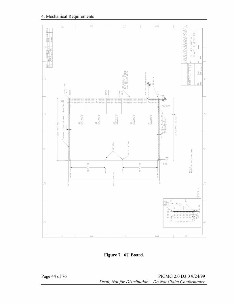
4. Mechanical Requirements
Page 44 of 76 PICMG 2.0 D3.0 9/24/99Draft, Not for Distribution – Do Not Claim Conformance
Figure 7. 6U Board.
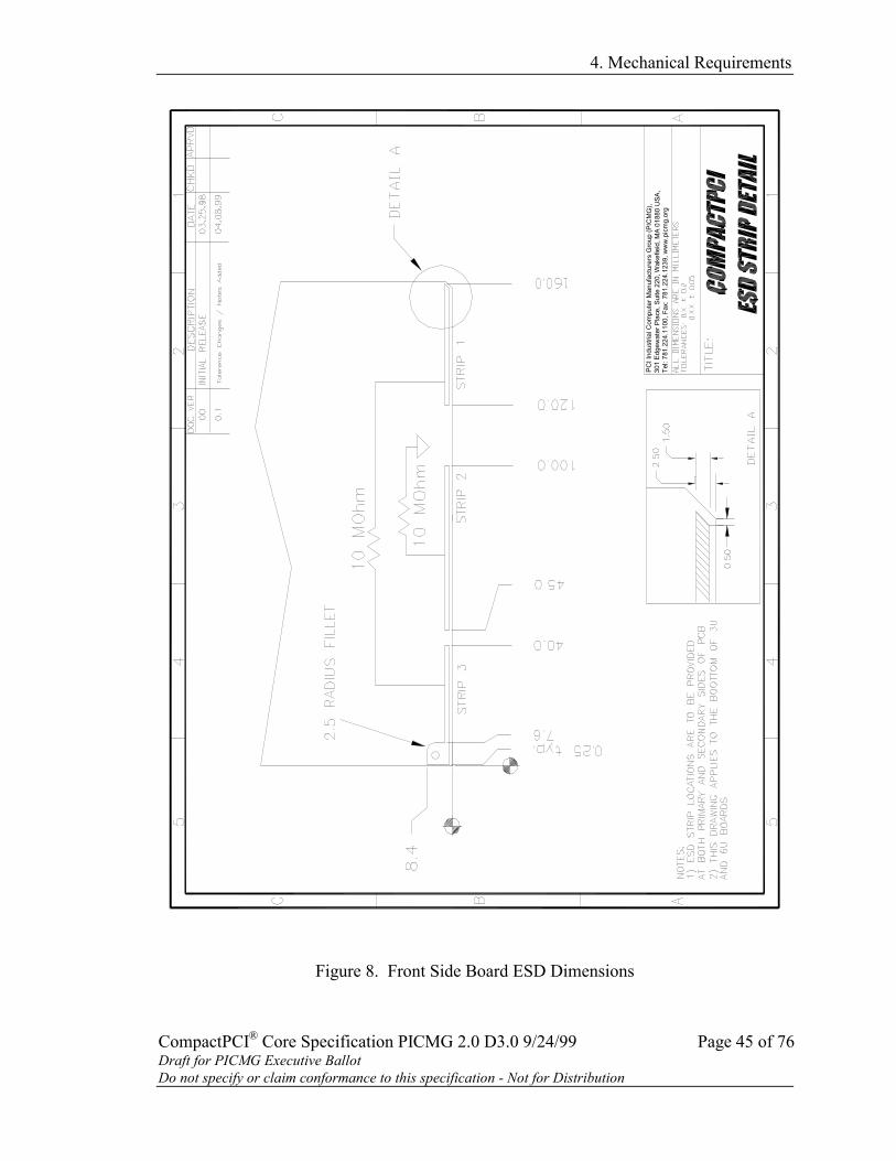
4. Mechanical Requirements
CompactPCI® Core Specification PICMG 2.0 D3.0 9/24/99 Page 45 of 76Draft for PICMG Executive BallotDo not specify or claim conformance to this specification - Not for Distribution
PCI I
ndus
trial
Com
pute
r Man
ufac
ture
rs G
roup
(PIC
MG
), 30
1 Ed
gew
ater
Pla
ce, S
uite
220
, Wak
efie
ld, M
A 01
880
USA
, Te
l: 78
1.22
4.11
00, F
ax: 7
81.2
24.1
239,
ww
w.p
icm
g.or
g
Figure 8. Front Side Board ESD Dimensions

4. Mechanical Requirements
Page 46 of 76 PICMG 2.0 D3.0 9/24/99Draft, Not for Distribution – Do Not Claim Conformance
Figure 9. 3U Rear-Panel I/O Board Dimensions

4. Mechanical Requirements
CompactPCI® Core Specification PICMG 2.0 D3.0 9/24/99 Page 47 of 76Draft for PICMG Executive BallotDo not specify or claim conformance to this specification - Not for Distribution
Figure 10. 6U Rear Panel I/O Board Dimensions

4. Mechanical Requirements
Page 48 of 76 PICMG 2.0 D3.0 9/24/99Draft, Not for Distribution – Do Not Claim Conformance
Figure 11. Rear Panel I/O ESD Dimensions
11/1
9/98
01C
HN
GD
TO
ALL
MET
RIC
DIM
,C
HN
GD
TITL
E BL
OC
K.
40.0
0.25 TYP
7.6
45.0
53.5
72.5
77.5
2.54
8.4
10 M
Ohm
10 M
Ohm
STRI
P 3
STRI
P 2
STRI
P 1
DET
AIL
A
4/24
/98
DAT
E
NO
TES:
1)
ESD
STR
IP L
OC
ATIO
NS
ARE
TO B
E PR
OVI
DED
A
T BO
TH P
RIM
ARY
AND
SEC
ON
DAR
Y SI
DES
OF
PCB.
2) O
NLY
THE
BO
TTO
M E
DG
E O
F H
OT
SWAP
BO
ARD
S
ARE
SPE
CIF
IED
FO
R ES
D S
TRIP
LO
CAT
ION
S. 3)
TH
IS D
RAW
ING
APP
LIES
TO
TH
E BO
TTO
M O
F 3U
A
ND
6U
BOAR
DS.
2
13
4
CC B A
12
45
B A
5
APR
VD
CH
KDD
ESC
RIPT
ION
DO
C V
ERRE
VISI
ON
S
00D
OC
UMEN
T O
RIG
INAT
ION
0.5
2.5
1.5
DET
AIL
A
02UP
DAT
ED D
IMEN
SIO
NS
TO M
ATC
HFR
ON
T ES
D S
TRIP,
TOLE
RAN
CE.
04/1
6/99
RAD
IUS
FILL
ET
3
ESD
STR
IP D
ETA
ILRE
AR P
ANEL
I/O
BO
ARD
DRA
WIN
G N
O.
TITLE
:
SCA
LE: N
ON
ED
ATE
:
CH
ECKE
D:
TOLE
RA
NC
ES:
DR
AWN
:
APP
ROVE
D:
X.X
= ±
0.2
ALL
DIM
ENSI
ON
S IN
MILL
IMET
ERS

4. Mechanical Requirements
CompactPCI® Core Specification PICMG 2.0 D3.0 9/24/99 Page 49 of 76Draft for PICMG Executive BallotDo not specify or claim conformance to this specification - Not for Distribution
TOP SHIELD
BACKPLANE
InterboardSeparation Plane
4.07
2.54
175.60 +/- 0.5
11.5
f
5 x 2.0
cde
ba
3.5
L Of Connector ('c' row)
2.0
C
eca b dz f
TOP VIEW
6 x 2.0
.XX = +/- 0.03
.X = +/- 0.1
CROSS SECTION
PRINTED CIRCUIT BOARD (PCB)
FRONT PANEL
(J)
FIXED RECEPTICAL (MALE)
FREE PLUG (FEMALE)
(P)
Figure 12. Cross Sectional Board, Connector, Backplane and Front Panel View.
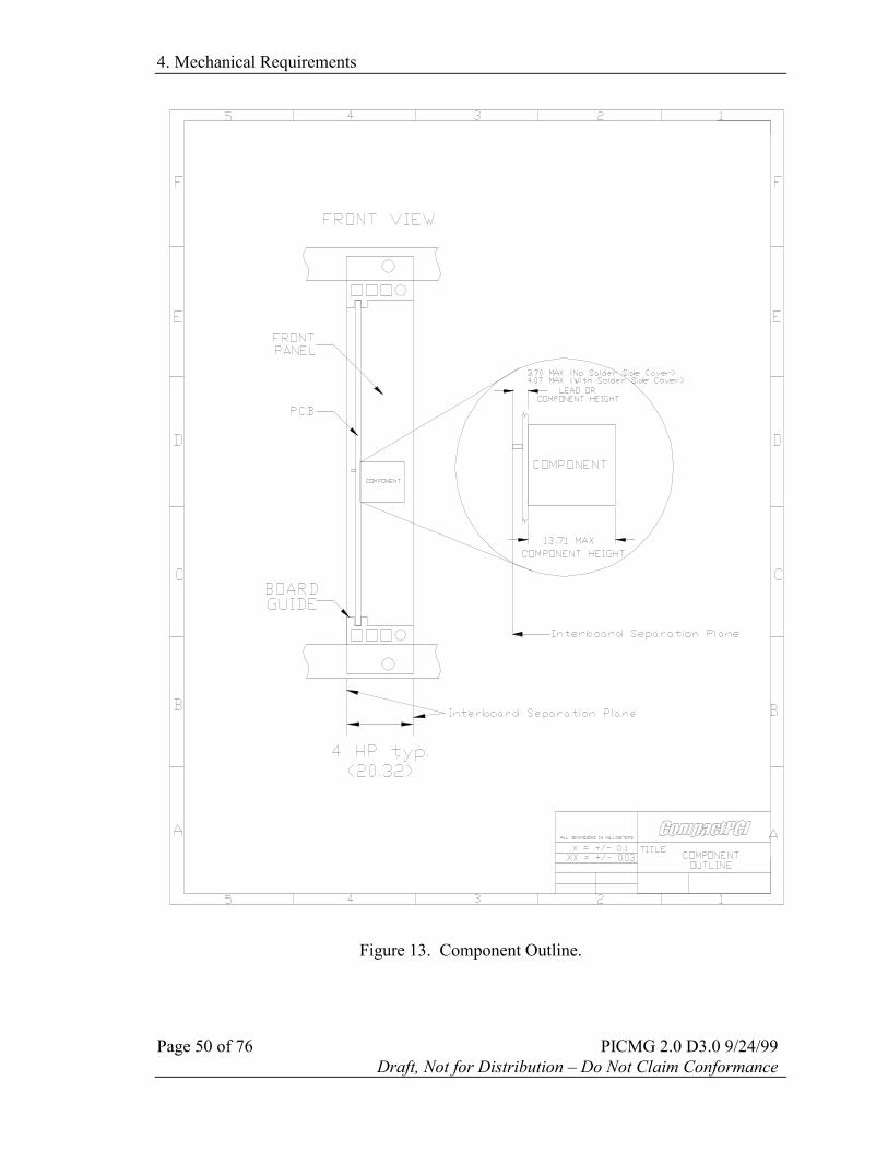
4. Mechanical Requirements
Page 50 of 76 PICMG 2.0 D3.0 9/24/99Draft, Not for Distribution – Do Not Claim Conformance
Figure 13. Component Outline.
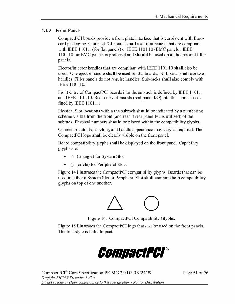
4. Mechanical Requirements
CompactPCI® Core Specification PICMG 2.0 D3.0 9/24/99 Page 51 of 76Draft for PICMG Executive BallotDo not specify or claim conformance to this specification - Not for Distribution
4.1.9 Front PanelsCompactPCI boards provide a front plate interface that is consistent with Euro-card packaging. CompactPCI boards shall use front panels that are compliantwith IEEE 1101.1 (for flat panels) or IEEE 1101.10 (EMC panels). IEEE1101.10 for EMC panels is preferred and should be used on all boards and fillerpanels.
Ejector/injector handles that are compliant with IEEE 1101.10 shall also beused. One ejector handle shall be used for 3U boards. 6U boards shall use twohandles. Filler panels do not require handles. Sub-racks shall also comply withIEEE 1101.10.
Front entry of CompactPCI boards into the subrack is defined by IEEE 1101.1and IEEE 1101.10. Rear entry of boards (real panel I/O) into the subrack is de-fined by IEEE 1101.11.
Physical Slot locations within the subrack should be indicated by a numberingscheme visible from the front (and rear if rear panel I/O is utilized) of thesubrack. Physical numbers should be placed within the compatibility glyphs.
Connector cutouts, labeling, and handle appearance may vary as required. TheCompactPCI logo shall be clearly visible on the front panel.
Board compatibility glyphs shall be displayed on the front panel. Capabilityglyphs are:
• (triangle) for System Slot
• (circle) for Peripheral Slots
Figure 14 illustrates the CompactPCI compatibility glyphs. Boards that can beused in either a System Slot or Peripheral Slot shall combine both compatibilityglyphs on top of one another.
Figure 14. CompactPCI Compatibility Glyphs.
Figure 15 illustrates the CompactPCI logo that shall be used on the front panels.The font style is Italic Impact.
CompactPCI CompactPCI CompactPCI CompactPCI ®

4. Mechanical Requirements
Page 52 of 76 PICMG 2.0 D3.0 9/24/99Draft, Not for Distribution – Do Not Claim Conformance
Figure 15. CompactPCI Logo.
4.1.9.1 3U Front Panels3U boards shall use one IEEE 1101.10 handle located on the bottom as il-lustrated in Figure 16.
4.1.9.2 6U Front Panels6U boards shall use two IEEE 1101.10 handles as illustrated in Figure 17.
4.1.10 System Slot Identification
System Slot capability shall be indicated within a CompactPCI subrack by redguide rails. This allows users to easily locate the System Slot. Peripheral slotsshall not use red guide rails.
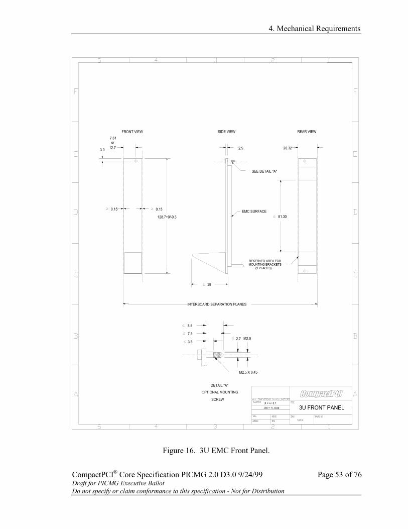
4. Mechanical Requirements
CompactPCI® Core Specification PICMG 2.0 D3.0 9/24/99 Page 53 of 76Draft for PICMG Executive BallotDo not specify or claim conformance to this specification - Not for Distribution
INTERBOARD SEPARATION PLANES
OPTIONAL MOUNTING
3.6
7.5
8.8
M2.52.7
DETAIL "A"
SCREW
.XX = +/- 0.03
.X = +/- 0.1
M2.5 X 0.45
3U FRONT PANEL
MOUNTING BRACKETS
38
RESERVED AREA FOR
(2 PLACES)
0.15
12.7or
3.0
0.15
128.7+0/-0.3
FRONT VIEW7.61
81.30
20.32
EMC SURFACE
SEE DETAIL "A"
2.5
SIDE VIEW REAR VIEW
Figure 16. 3U EMC Front Panel.
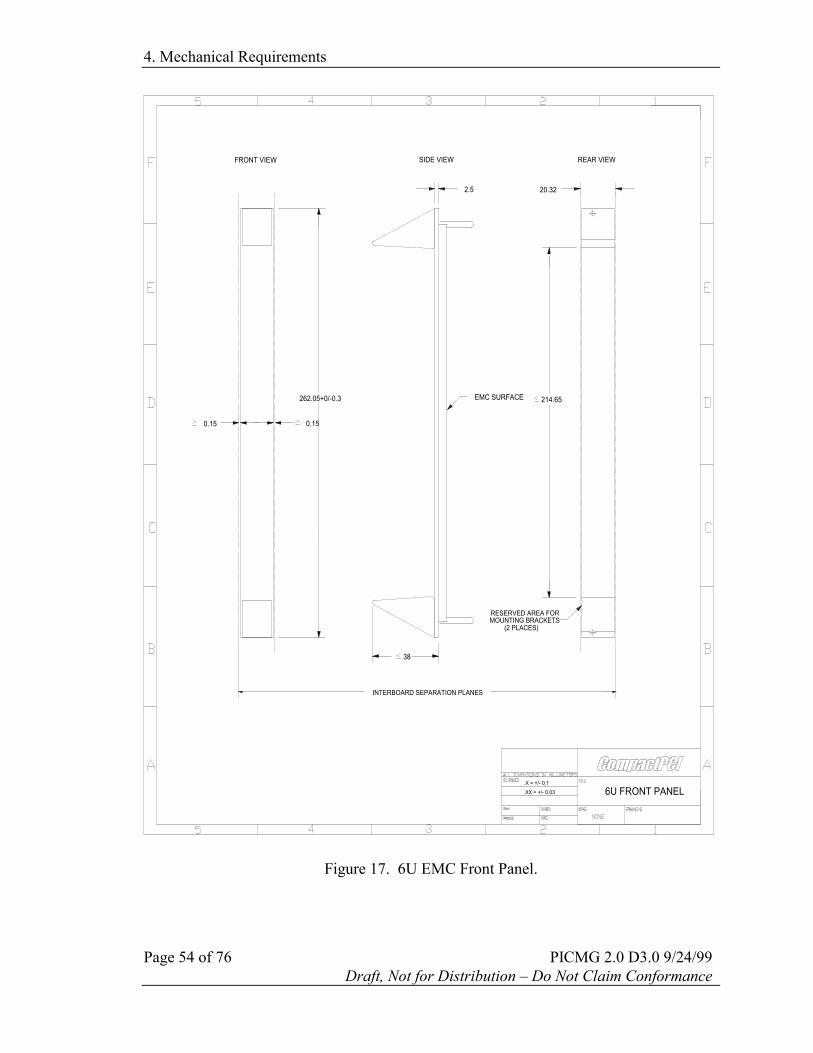
4. Mechanical Requirements
Page 54 of 76 PICMG 2.0 D3.0 9/24/99Draft, Not for Distribution – Do Not Claim Conformance
38
INTERBOARD SEPARATION PLANES
.XX = +/- 0.03
.X = +/- 0.1
6U FRONT PANEL
MOUNTING BRACKETSRESERVED AREA FOR
(2 PLACES)
0.15
262.05+0/-0.3
0.15
FRONT VIEW
214.65EMC SURFACE
SIDE VIEW
2.5 20.32
REAR VIEW
Figure 17. 6U EMC Front Panel.

4. Mechanical Requirements
CompactPCI® Core Specification PICMG 2.0 D3.0 9/24/99 Page 55 of 76Draft for PICMG Executive BallotDo not specify or claim conformance to this specification - Not for Distribution
4.2 Rear-Panel I/O Board RequirementsThe front plug-in boards may route I/O through the backplane via the J2/P2, J3/P3,J4/P4 and J5/P5 connector pairs, using any combination of connectors. In many ap-plications, the only practical way to route this I/O off the backplane is to utilize a rearI/O transition board that has standard I/O connectors for each particular type of I/O.
4.2.1 MechanicalsIEEE 1101.11 defines the generic mechanics for rear-panel I/O transitionboards. The mechanical implementation of rear-panel I/O transition boards andsubracks should be in accordance to IEEE 1101.11 for 80 mm deep boards andsubracks (also see Section 4.1.3).
The same front panel, the same handles, the same keying, the same alignmentpin, the same EMC and the same ESD mechanics should be used as on the frontCompactPCI boards.
The same subrack rails, card guides, EMC support, ESD support, keying, align-ment pin hole, and injector/extractor comb should be used as on the subrackfront side, except for the card guide's depth.
Note that rear-panel I/O transition boards are "in-line" with the front Com-pactPCI boards. This means that the front panels of rear-panel I/O transitionboards are reversed (mirrored) from the front boards. The top handles are on thebottom and the bottom handles are on the top. The slot keying holes and holelabels in both the card guides and front panels will be upside down as comparedto the front boards and card guides.
The same connector pin labeling sequence should be used on the rear I/O transi-tion boards as the on front boards, with the position numbers going from bottomto top. Effectively this is a mirror image of the front board’s layout orientation.By using the same 1 for 1 pin mapping labeling sequence eliminates confusionand I/O signal pin mapping problems. Example, pin J5:A3 of the front boardconnects to P5:A3 of the backplane, the signal is available as rP5:A3 from therear of the backplane, and connects to rJ5:A3 of the rear I/O module.
Note that
Figure 9 and Figure 10, illustrating 3U and 6U rear-panel I/O boards, show rJ1for mechanical reference only.
4.2.2 PowerIn some applications, the rear-panel transition board will have active compo-nents. Power can be applied either through the I/O pins from the front board, orfrom the normal power and ground pins defined as part of the J1/P1 and J2/P2connector pin assignments.

4. Mechanical Requirements
Page 56 of 76 PICMG 2.0 D3.0 9/24/99Draft, Not for Distribution – Do Not Claim Conformance
4.2.3 Rear Panel Keying
Rear panel I/O boards shall be keyed in accordance with the PICMG 2.10Keying of CompactPCI Boards and Backplanes specification.
4.3 Backplane Requirements
4.3.1 Connector OrientationThe bus segment connector orientation is illustrated in Figure 18 when viewedfrom the front of the system chassis. The System Slot may be located in any po-sition on a backplane but shall be located on either end of the bus segment un-less otherwise simulated to ensure compliance to the PCI specification.
Figure 18. 3U Backplane Example - Front View.
4.3.2 Slot SpacingThis specification and all backplane simulations have assumed a linear topologyusing 20.32 mm (0.8 inch) board center-to-center spacing. Any other topologyshall be simulated or otherwise verified to ensure compliance to the PCI specifi-cation.
Bus segments shall not have more than eight slots without one or more PCIbridges.
= PERIPHERAL SLOT
1
3edcz a b f
1
12-P1
2
25
4 5
= SYSTEM SLOT22
2-P2
1
7-P1
76cz a b d e f
8
1
25
7-P222

4. Mechanical Requirements
CompactPCI® Core Specification PICMG 2.0 D3.0 9/24/99 Page 57 of 76Draft for PICMG Executive BallotDo not specify or claim conformance to this specification - Not for Distribution
4.3.3 Slot Designation
Physical backplane slots shall be designated 1, 2, 3, through N, where N is thenumber of slots. For example, an eight slot backplane would designate the back-plane slots as 1 through 8 with the compatibility glyphs. Slot numbering shallstart at the top left corner as viewed from the front.
Logical slot numbers shall be defined by the IDSEL and associated address usedto select the slot as defined in Table 7. Logical slot numbers are used in the no-menclature to define the physical outline of a connector on a bus segment. Pleasesee Chapter 3 for signal routing requirements.
Each slot may be implemented with one or more connectors. Backplane connec-tors shall be designated as P1 through P5, corresponding in location to theboard’s connectors illustrated in Figure 6 and Figure 7.
Any given connector shall be referenced by first specifying the logical slot num-ber (1...8) followed by a hyphen and then the individual connector (P1...P5). Forexample, in a 32-bit 3U system 5-P2 would designate the rear-panel I/O con-nector in logical slot 5. In a 64-bit 6U system 1-P3 would designate the rear-panel I/O connector in logical slot 1.
4.3.4 Bus Segments
Bus segments may accommodate 64-bit operation or shall provide individualpull-up resistors at each board slot for the REQ64# and ACK64# signals. Referto the PCI specification for details. The System Slot shall use both J1 and J2 toallow the arbitration and clock signals to be connected to the backplane from aSystem Slot board. Connectors require pin staging (see Section 5.8) to accom-modate hot swap operation.
CompactPCI bus segments shall bus all signals in all slots within the segmentexcept the slot specific signals: CLK, REQ# and GNT#. Each logical slot alsohas a unique IDSEL signal connected to one of the upper ADxx signals for con-figuration (plug and play) decoding.
Backplanes shall provide connection for the DEG#(P2:C16) and FAL# (P2:C15)signals at the System Slot that may be provided by the power supply or othersystem management functions.
4.3.5 Backplane DimensionsDepending on system design requirements, termination networks, etc., the leftand right ends of a backplane can be made longer. Whenever extended, the enddimensions shall be in increments of 5.08 mm. This will allow for modular con-struction of backplanes and subracks.

4. Mechanical Requirements
Page 58 of 76 PICMG 2.0 D3.0 9/24/99Draft, Not for Distribution – Do Not Claim Conformance
4.3.5.1 3U BackplanesA 3U backplane without a power connector is illustrated in Figure 19. Thisfigure illustrates physical slot locations designated 1 through 8.
4.3.5.2 6U BackplanesA 6U backplane without a power connector is illustrated in Figure 20. Physi-cal slot locations are designated 1 through 8.
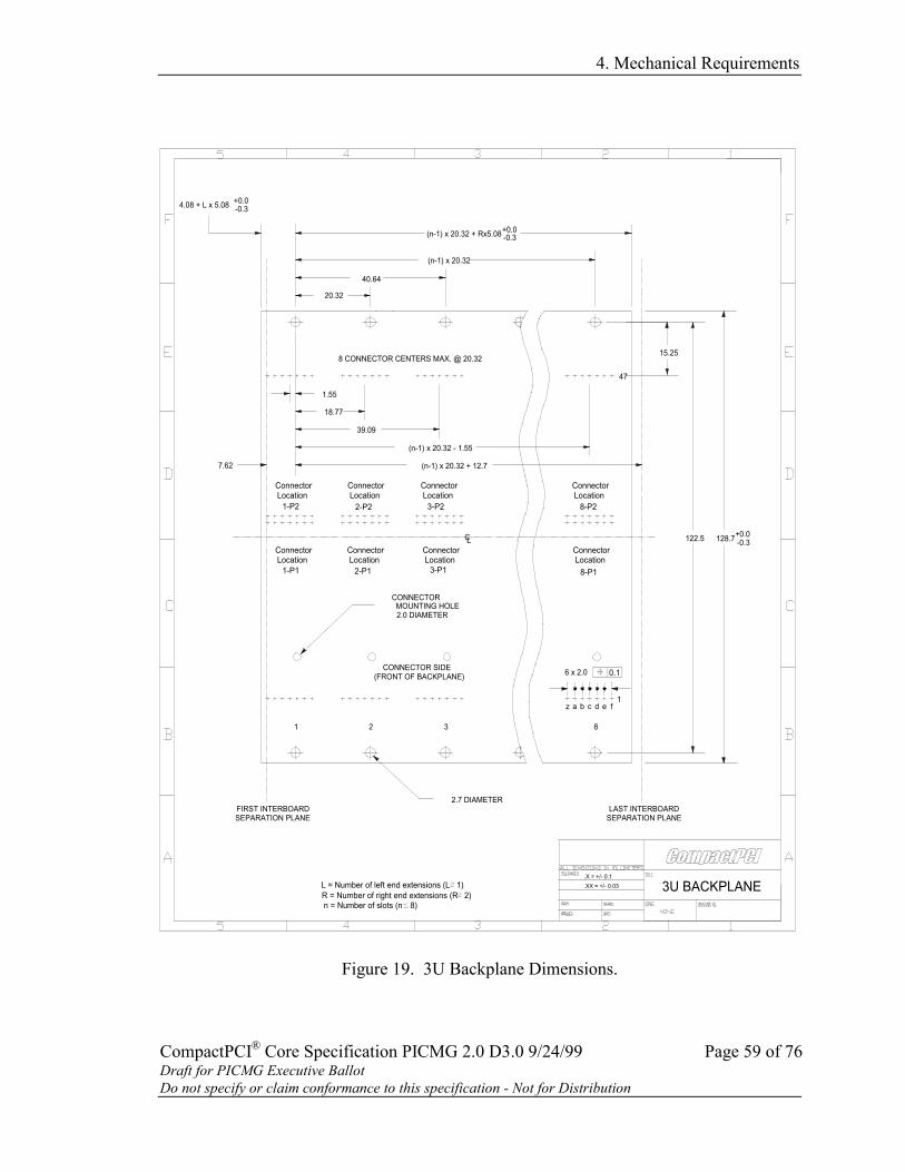
4. Mechanical Requirements
CompactPCI® Core Specification PICMG 2.0 D3.0 9/24/99 Page 59 of 76Draft for PICMG Executive BallotDo not specify or claim conformance to this specification - Not for Distribution
3 81 2
2.7 DIAMETER
R = Number of right end extensions (R
(FRONT OF BACKPLANE)
MOUNTING HOLE
LocationConnector
SEPARATION PLANEFIRST INTERBOARD
L = Number of left end extensions (L
n = Number of slots (n 8)
LocationConnector
CONNECTOR SIDE
1-P1Location
2-P1
Connector
CONNECTOR
2.0 DIAMETER
3-P1
SEPARATION PLANELAST INTERBOARD
1)2)
.XX = +/- 0.03
.X = +/- 0.1
3U BACKPLANE
dz ba c1
fe
0.16 x 2.0
LC
Location8-P1
Connector-0.3128.7122.5 +0.0
ConnectorLocation
8 CONNECTOR CENTERS MAX. @ 20.32
(n-1) x 20.32 + Rx5.08
(n-1) x 20.32
(n-1) x 20.32 - 1.55
(n-1) x 20.32 + 12.7
ConnectorLocation
7.62
1-P2
ConnectorLocation
2-P2
39.09
3-P2
1.55
18.77
+0.04.08 + L x 5.08 -0.3
40.64
20.32
47
ConnectorLocation
8-P2
15.25
-0.3+0.0
Figure 19. 3U Backplane Dimensions.
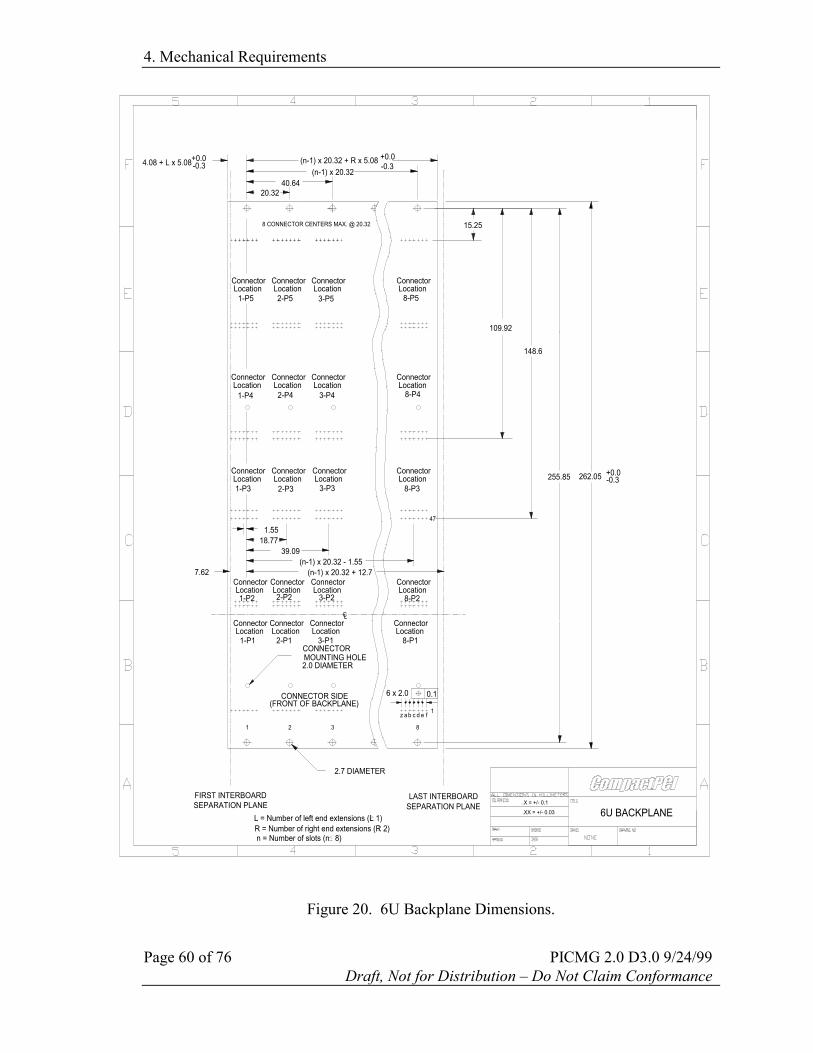
4. Mechanical Requirements
Page 60 of 76 PICMG 2.0 D3.0 9/24/99Draft, Not for Distribution – Do Not Claim Conformance
Figure 20. 6U Backplane Dimensions.
LAST INTERBOARDSEPARATION PLANE
ConnectorLocation
ConnectorLocation
0.1
1
47
2.0 DIAMETER
3 81 2
L = Number of left end extensions (LR = Number of right end extensions (Rn = Number of slots (n
FIRST INTERBOARDSEPARATION PLANE
2.7 DIAMETER
1)2)
8)
ba
6 x 2.0(FRONT OF BACKPLANE)
CONNECTOR SIDE
z c d e f
ConnectorLocation
ConnectorLocation
ConnectorLocation
ConnectorLocation
ConnectorLocation
1.5518.77
1-P1
1-P2
7.62
ConnectorLocation1-P3
(n-1) x 20.32 - 1.55
ConnectorLocation
8-P1
8-P2
ConnectorLocation
CONNECTORMOUNTING HOLE
2-P1 3-P1
ConnectorLocation
CL
2-P2 3-P2
(n-1) x 20.32 + 12.7
8-P3
39.09
ConnectorLocation
2-P3 3-P3
.XX = +/- 0.03
.X = +/- 0.1
6U BACKPLANE
262.05255.85 -0.3+0.0
ConnectorLocation
ConnectorLocation
ConnectorLocation
ConnectorLocation
ConnectorLocation
1-P4
ConnectorLocation
1-P5
8-P4
ConnectorLocation
2-P4 3-P4
8-P5
ConnectorLocation
2-P5 3-P5
20.32
8 CONNECTOR CENTERS MAX. @ 20.32
-0.3+0.04.08 + L x 5.08
40.64
(n-1) x 20.32 + R x 5.08-0.3+0.0
(n-1) x 20.32
148.6
109.92
15.25

4. Mechanical Requirements
CompactPCI® Core Specification PICMG 2.0 D3.0 9/24/99 Page 61 of 76Draft for PICMG Executive BallotDo not specify or claim conformance to this specification - Not for Distribution
5 Connector ImplementationAll 3U/6U CompactPCI boards and backplanes shall follow the connectorimplementation shown in Figure 21 and Figure 22. The connectors belong to the 2 mmhard metric family as defined by IEC 61076-4-101. Appendix B summarizes theconnector implementation, and the connector pin numbering regime.
Figure 21. 3U Connector Implementation
Figure 22. 6U Connector Implementation

5. Connector Implementation
Page 62 of 76 PICMG 2.0 D3.0 9/24/99Draft, Not for Distribution – Do Not Claim Conformance
5.1 Overview
5.1.1 LocationConnector locations are designated from bottom to top by numbers 1 to 5. Theprefix “J” is assigned to connectors on front plug-in boards. The prefix “P” isassigned to connectors on the front side of backplane. The prefix “rP” is assignedto connectors on the rear side of backplane. The prefix “rJ” is assigned toconnectors on rear-panel I/O boards.
5.1.2 Housing TypesConnector housing types are designated by Type A, Type B, and Type AB. TypeA connectors have alignment features and coding keys. Type B connectors areplain without these features. Type AB connectors have alignment featureswithout coding keys. The Type AB connector is new and has not beenincorporated into the IEC specifications at the date of this writing, see PICMGType AB 2mm Connector Guideline Document for information.
To avoid confusion, all products involving rear panel I/O boards (boards, systems,backplanes, etc) should clearly state in customer documentation which level ofcompliance the product conforms to, either Revision 2.X or Revision 3.X of theCompactPCI specification.
System and backplane vendors shall use Type AB shrouds in locationsrP2/rP3/rP5 to insure backward compatibility with legacy rear panel I/O boardsand forward compatibility with rear panel I/O boards being produced today.
Refer to Appendix B for more information on 2mm Connector usage.
5.1.3 Connector Tail LengthsIn CompactPCI connector implementations, feed-to connectors are defined asconnectors that interface to the front side of the backplane only and do not extendthrough the backplane. Feed-thru connectors are defined as having long tails thatextend through the backplane for rear-panel I/O interfacing.
Connectors defined for rear-panel I/O shall have feed-thru tails of 16mm length.Connectors that are not defined for rear-panel I/O shall be feed-to.
5.1.4 Backplane / Board Population OptionsAt a minimum, the J1 connector is required for 32-bit CompactPCI and J2 isrequired for the additional 64-bit CompactPCI signals. The other connectors mayor may not be populated depending upon the system requirements. See thevarious platform specifications for their specific connector populationrequirements.

4. Mechanical Requirements
CompactPCI® Core Specification PICMG 2.0 D3.0 9/24/99 Page 63 of 76Draft for PICMG Executive BallotDo not specify or claim conformance to this specification - Not for Distribution
5.2 J1 (32-Bit PCI Signals)CompactPCI board connector J1 is used for the 32-bit PCI signals as illustrated inTable 13. 32-bit boards shall always use this connector. Use of the J2 connector isoptional.
5.3 J2 ConnectorJ2 may be used for 64-bit PCI transfers or for rear-panel I/O. The keying of this con-nector function is provided by the IEEE 1101.10 front panel key. J2 shall be used onSystem Slot boards to provide arbitration and clock signals for peripheral boards. J2shall be used if 64-bit PCI operation, rear-panel I/O, or geographic addressing issupported.
5.3.1 Peripheral Slot 64-Bit PCI
The mapping of 64-bit PCI within J2 is shown in Table 13.
5.3.2 Peripheral Slot Rear-Panel I/O
The mapping of rear-panel I/O for peripheral boards within J2 is shown in Table14.
5.3.3 System Slot 64-bit PCI
The mapping of 64-Bit PCI for the system slot is shown in Table 15.
5.3.4 System Slot Rear-Panel I/O
The mapping of rear-panel I/O for system slot boards is shown in Table 16.
5.4 Bussed Reserved PinsThe BRSVPxxx signals shall be bussed between connectors and are reserved for fu-ture definition.
5.5 Non-Bussed Reserved PinsThe RSV signals shall be non-bussed between connectors and are reserved for futuredefinition.
5.6 Power PinsAll CompactPCI connectors provide pins for +5V, +3.3V, +12V and -12V operatingpower. Additional power pins labeled +V(I/O) provide power for Universal boardsutilizing I/O buffers driving backplane signals that may operate from +5V or +3.3V.

5. Connector Implementation
Page 64 of 76 PICMG 2.0 D3.0 9/24/99Draft, Not for Distribution – Do Not Claim Conformance
On these boards, the PCI component’s I/O buffers shall be powered from V(I/O), notfrom +5V or +3.3V power pins.
Backplane pins labeled V(I/O) are connected to +5V on 5 V keyed systems and+3.3V on 3.3 V keyed systems. Alternatively, a separate V(I/O) power plane may beprovided to supply 5 V or 3.3 V power.
The IEC 61076-4-101 connector is a press-fit connector. Connections between thevoltage planes and connector pins should be a solid (no thermal relief) interconnect.This provides a low inductance connection between the connector pin and eachpower plane.
5.7 5V/3.3V PCI KeyingCompactPCI implements a keying mechanism to differentiate 5 V or 3.3 V signalingoperation. The keying mechanism is designed to prevent a board built with onebuffer technology (5 V or 3.3 V) from being inserted into a system designed for theother buffer technology (3.3 V or 5 V, respectively). Universal boards may operatein either +5V or +3.3V systems and are not keyed. Positions 12-14 of the Com-pactPCI connector are used for the keying mechanism. Backplanes shall be config-ured as either 5V or 3.3V and shall provide the appropriate key. It is not possible tohave a “universal” backplane. Refer to the PICMG 2.10, Keying of CompactPCIBoards and Backplanes specification for additional details on keying.
Table 12. Coding Key Color Assignments and Part Numbers.
Signaling Voltage Color Reference Code #
V(I/O) Color RAL # (1) Male (Back-plane)
Female(Board)
3.3 V CadmiumYellow
1021 3456 1278
5 V BrilliantBlue
5007 1567 2348
3.3 V or 5 V(Universal Board)
- - N/A(2) No Key
Notes:
1. RAL is a trademark of the central organization for product assurance in Germany. One of itstasks is harmonization in the use of colors. Color samples may be ordered from: Muster-Schmidt KG, RAL - Farbkartenvertrieb, Postfach 2751, D - 3400 Gottingen, Germany.
2. Backplanes shall be configured for either 5 V or 3.3 V V(I/O). Plug in boards may be de-signed to be universal and shall therefore have no key loaded.

4. Mechanical Requirements
CompactPCI® Core Specification PICMG 2.0 D3.0 9/24/99 Page 65 of 76Draft for PICMG Executive BallotDo not specify or claim conformance to this specification - Not for Distribution
5.8 Pin AssignmentsTable 13. CompactPCI Peripheral Slot 64-Bit Connector Pin Assignments(1)(10, 11).
22 GND GA4(13) GA3(13) GA2(13) GA1(13) GA0(13) GND21 GND RSV RSV RSV RSV RSV GND20 GND RSV RSV RSV GND RSV GND19 GND RSV RSV RSV RSV RSV GND P218 GND BRSVP2A18 BRSVP2B18 BRSVP2C18 GND BRSVP2E18 GND /17 GND BRSVP2A17 GND RSV RSV RSV GND J216 GND BRSVP2A16 BRSVP2B16 RSV GND BRSVP2E16 GND15 GND BRSVP2A15 GND RSV RSV RSV GND14 GND AD[35] AD[34] AD[33] GND AD[32] GND13 GND AD[38] GND V(I/O)(2) AD[37] AD[36] GND C12 GND AD[42] AD[41] AD[40] GND AD[39] GND O11 GND AD[45] GND V(I/O)(2) AD[44] AD[43] GND N10 GND AD[49] AD[48] AD[47] GND AD[46] GND N9 GND AD[52] GND V(I/O)(2) AD[51] AD[50] GND E8 GND AD[56] AD[55] AD[54] GND AD[53] GND C7 GND AD[59] GND V(I/O)(2) AD[58] AD[57] GND T6 GND AD[63] AD[62] AD[61] GND AD[60] GND O5 GND C/BE[5]# GND V(I/O)(2) C/BE[4]# PAR64 GND R4 GND V(I/O)(2) BRSVP2B4 C/BE[7]# GND C/BE[6]# GND
3(3) GND RSV GND RSV RSV RSV GND2(3) GND RSV RSV UNC(4) RSV RSV GND1(3) GND RSV GND RSV RSV RSV GND25 GND 5V REQ64# ENUM# 3.3V 5V GND24 GND AD[1] 5V V(I/O)(2),(6) AD[0] ACK64# GND23 GND 3.3V AD[4] AD[3] 5V(6) AD[2] GND22 GND AD[7] GND 3.3V(6) AD[6] AD[5] GND P121 GND 3.3V AD[9] AD[8] M66EN(5) C/BE[0]# GND /20 GND AD[12] GND V(I/O)(2) AD[11] AD[10] GND J119 GND 3.3V AD[15] AD[14] GND(6) AD[13] GND18 GND SERR# GND 3.3V PAR C/BE[1]# GND17 GND 3.3V IPMB SCL IPMB SDA GND(6) PERR# GND16 GND DEVSEL# GND V(I/O)(2) STOP# LOCK# GND C15 GND 3.3V FRAME# IRDY# BD SEL#(7) TRDY# GND O
12-14 KEY AREA N11 GND AD[18] AD[17] AD[16] GND(6) C/BE[2]# GND N10 GND AD[21] GND 3.3V AD[20] AD[19] GND E9 GND C/BE[3]# IDSEL(7) AD[23] GND(6) AD[22] GND C8 GND AD[26] GND V(I/O)(2) AD[25] AD[24] GND T7 GND AD[30] AD[29] AD[28] GND(6) AD[27] GND O6 GND REQ# GND 3.3V(6) CLK AD[31] GND R5 GND BRSVP1A5 BRSVP1B5 RST# GND(6) GNT# GND4 GND IPMB PWR HEALTHY# (18) V(I/O)(2),(6) INTP INTS GND3 GND INTA# INTB# INTC# 5V(6) INTD# GND2 GND TCK(15) 5V TMS(15) TDO(15) TDI(15) GND1 GND 5V -12V TRST#(15) +12V 5V GND
Pin Z(14) A B C D E F(9)
= long pins (front only) = short pins (front only) = medium length pins (front only)
Notes: (See page 69)

5. Connector Implementation
Page 66 of 76 PICMG 2.0 D3.0 9/24/99Draft, Not for Distribution – Do Not Claim Conformance
Table 14 CompactPCI Peripheral Slot Rear-Panel I/O Connector Pin Assignments(1)(3)(8, 9)
22 GND GA4(13) GA3(13) GA2(13) GA1(13) GA0(13) GND21 GND BP(I/O) BP(I/O) BP(I/O) BP(I/O) BP(I/O) GND20 GND BP(I/O) BP(I/O) BP(I/O) BP(I/O) BP(I/O) GND19 GND BP(I/O) BP(I/O) BP(I/O) BP(I/O) BP(I/O) GND18 GND BP(I/O) BP(I/O) BP(I/O) BP(I/O) BP(I/O) GND P217 GND BP(I/O) BP(I/O) BP(I/O) BP(I/O) BP(I/O) GND /16 GND BP(I/O) BP(I/O) BP(I/O) BP(I/O) BP(I/O) GND J215 GND BP(I/O) BP(I/O) BP(I/O) BP(I/O) BP(I/O) GND14 GND BP(I/O) BP(I/O) BP(I/O) BP(I/O) BP(I/O) GND13 GND BP(I/O) BP(I/O) BP(I/O) BP(I/O) BP(I/O) GND C12 GND BP(I/O) BP(I/O) BP(I/O) BP(I/O) BP(I/O) GND O11 GND BP(I/O) BP(I/O) BP(I/O) BP(I/O) BP(I/O) GND N10 GND BP(I/O) BP(I/O) BP(I/O) BP(I/O) BP(I/O) GND N9 GND BP(I/O) BP(I/O) BP(I/O) BP(I/O) BP(I/O) GND E8 GND BP(I/O) BP(I/O) BP(I/O) BP(I/O) BP(I/O) GND C7 GND BP(I/O) BP(I/O) BP(I/O) BP(I/O) BP(I/O) GND T6 GND BP(I/O) BP(I/O) BP(I/O) BP(I/O) BP(I/O) GND O5 GND BP(I/O) BP(I/O) BP(I/O) BP(I/O) BP(I/O) GND R4 GND BP(I/O) BP(I/O) BP(I/O) BP(I/O) BP(I/O) GND3 GND BP(I/O) BP(I/O) BP(I/O) BP(I/O) BP(I/O) GND2 GND BP(I/O) BP(I/O) BP(I/O) BP(I/O) BP(I/O) GND1 GND BP(I/O) BP(I/O) BP(I/O) BP(I/O) BP(I/O) GND25 GND 5V REQ64# ENUM# 3.3V 5V GND24 GND AD[1] 5V V(I/O)(2),(6) AD[0] ACK64# GND23 GND 3.3V AD[4] AD[3] 5V(6) AD[2] GND22 GND AD[7] GND 3.3V(6) AD[6] AD[5] GND P121 GND 3.3V AD[9] AD[8] M66EN(5) C/BE[0]# GND /20 GND AD[12] GND V(I/O)(2) AD[11] AD[10] GND J119 GND 3.3V AD[15] AD[14] GND(6) AD[13] GND18 GND SERR# GND 3.3V PAR C/BE[1]# GND17 GND 3.3V IPMB SCL IPMB SDA GND(6) PERR# GND16 GND DEVSEL# GND V(I/O)(2) STOP# LOCK# GND C15 GND 3.3V FRAME# IRDY# BD SEL#(7) TRDY# GND O
12-14 KEY AREA N11 GND AD[18] AD[17] AD[16] GND(6) C/BE[2]# GND N10 GND AD[21] GND 3.3V AD[20] AD[19] GND E9 GND C/BE[3]# IDSEL(7) AD[23] GND(6) AD[22] GND C8 GND AD[26] GND V(I/O)(2) AD[25] AD[24] GND T7 GND AD[30] AD[29] AD[28] GND(6) AD[27] GND O6 GND REQ# GND 3.3V(6) CLK AD[31] GND R5 GND BRSVP1A5 BRSVP1B5 RST# GND(6) GNT# GND4 GND IPMB PWR HEALTHY# (18) V(I/O)(2),(6) INTP INTS GND3 GND INTA# INTB# INTC# 5V(6) INTD# GND2 GND TCK(15) 5V TMS(15) TDO(15) TDI(15) GND1 GND 5V -12V TRST#(15) +12V 5V GND
Pin Z(14) A B C D E F(9)
= long pins (front only) = short pins (front only) = medium length pins (front only)
Notes: (See page 69)

4. Mechanical Requirements
CompactPCI® Core Specification PICMG 2.0 D3.0 9/24/99 Page 67 of 76Draft for PICMG Executive BallotDo not specify or claim conformance to this specification - Not for Distribution
Table 15. CompactPCI System Slot 64-bit Connector Pin Assignment
22 GND GA4(13) GA3(13) GA2(13) GA1(13) GA0(13) GND21 GND CLK6 GND RSV RSV RSV GND20 GND CLK5 GND RSV GND RSV GND19 GND GND GND RSV(16) RSV(16) RSV(16) GND P218 GND BRSVP2A18 BRSVP2B18 BRSVP2C18 GND BRSVP2E18 GND /17 GND BRSVP2A17 GND PRST# REQ6# GNT6# GND J216 GND BRSVP2A16 BRSVP2B16 DEG# GND BRSVP2E16 GND15 GND BRSVP2A15 GND FAL# REQ5# GNT5# GND14 GND AD[35] AD[34] AD[33] GND AD[32] GND13 GND AD[38] GND V(I/O)(2) AD[37] AD[36] GND C12 GND AD[42] AD[41] AD[40] GND AD[39] GND O11 GND AD[45] GND V(I/O)(2) AD[44] AD[43] GND N10 GND AD[49] AD[48] AD[47] GND AD[46] GND N9 GND AD[52] GND V(I/O)(2) AD[51] AD[50] GND E8 GND AD[56] AD[55] AD[54] GND AD[53] GND C7 GND AD[59] GND V(I/O)(2) AD[58] AD[57] GND T6 GND AD[63] AD[62] AD[61] GND AD[60] GND O5 GND C/BE[5]# GND V(I/O)(2) C/BE[4]# PAR64 GND R4 GND V(I/O)(2) BRSVP2B4 C/BE[7]# GND C/BE[6]# GND
3(3) GND CLK4 GND GNT3# REQ4# GNT4# GND2(3) GND CLK2 CLK3 SYSEN#(4) GNT2# REQ3# GND1(3) GND CLK1 GND REQ1# GNT1# REQ2# GND25 GND 5V REQ64# ENUM# 3.3V 5V GND24 GND AD[1] 5V V(I/O)(2),(6) AD[0] ACK64# GND23 GND 3.3V AD[4] AD[3] 5V(6) AD[2] GND22 GND AD[7] GND 3.3V(6) AD[6] AD[5] GND P121 GND 3.3V AD[9] AD[8] M66EN(5) C/BE[0]# GND /20 GND AD[12] GND V(I/O)(2) AD[11] AD[10] GND J119 GND 3.3V AD[15] AD[14] GND(6) AD[13] GND18 GND SERR# GND 3.3V PAR C/BE[1]# GND17 GND 3.3V IPMB SCL IPMB SDA GND(6) PERR# GND16 GND DEVSEL# GND V(I/O)(2) STOP# LOCK# GND C15 GND 3.3V FRAME# IRDY# GND TRDY# GND O
12-14 KEY AREA N11 GND AD[18] AD[17] AD[16] GND(6) C/BE[2]# GND N10 GND AD[21] GND 3.3V AD[20] AD[19] GND E9 GND C/BE[3]# GND AD[23] GND(6) AD[22] GND C8 GND AD[26] GND V(I/O)(2) AD[25] AD[24] GND T7 GND AD[30] AD[29] AD[28] GND(6) AD[27] GND O6 GND REQ0# GND 3.3V(6) CLK0 AD[31] GND R5 GND BRSVP1A5 BRSVP1B5 RST# GND(6) GNT0# GND4 GND IPMB PWR HEALTHY# (18) V(I/O)(2),(6) INTP INTS GND3 GND INTA# INTB# INTC# 5V(6) INTD# GND2 GND TCK(15) 5V TMS(15) TDO(15) TDI(15) GND1 GND 5V -12V TRST#(15) +12V 5V GND
Pin Z(14) A B C D E F(9)
= long pins (front only) = short pins (front only) = medium length pins (front only)
Notes: (See page 69)

5. Connector Implementation
Page 68 of 76 PICMG 2.0 D3.0 9/24/99Draft, Not for Distribution – Do Not Claim Conformance
Table 16. CompactPCI System Slot Rear-Panel I/O Connector Pin Assignments.
22 GND GA4(13) GA3(13) GA2(13) GA1(13) GA0(13) GND21 GND CLK6 GND BP(I/O) BP(I/O) BP(I/O) GND20 GND CLK5 GND BP(I/O) BP(I/O) BP(I/O) GND19 GND GND GND BP(I/O)(16) BP(I/O)(16) BP(I/O)(16) GND P218 GND BP(I/O) BP(I/O) BP(I/O) BP(I/O) BP(I/O) GND /17 GND BP(I/O) BP(I/O) PRST# REQ6# GNT6# GND J216 GND BP(I/O) BP(I/O) DEG# GND BP(I/O) GND15 GND BP(I/O) BP(I/O) FAL# REQ5# GNT5# GND14 GND BP(I/O) BP(I/O) BP(I/O) BP(I/O) BP(I/O) GND13 GND BP(I/O) BP(I/O) BP(I/O) BP(I/O) BP(I/O) GND C12 GND BP(I/O) BP(I/O) BP(I/O) BP(I/O) BP(I/O) GND O11 GND BP(I/O) BP(I/O) BP(I/O) BP(I/O) BP(I/O) GND N10 GND BP(I/O) BP(I/O) BP(I/O) BP(I/O) BP(I/O) GND N9 GND BP(I/O) BP(I/O) BP(I/O) BP(I/O) BP(I/O) GND E8 GND BP(I/O) BP(I/O) BP(I/O) BP(I/O) BP(I/O) GND C7 GND BP(I/O) BP(I/O) BP(I/O) BP(I/O) BP(I/O) GND T6 GND BP(I/O) BP(I/O) BP(I/O) BP(I/O) BP(I/O) GND O5 GND BP(I/O) BP(I/O) BP(I/O) BP(I/O) BP(I/O) GND R4 GND V(I/O) BP(I/O) BP(I/O) BP(I/O) BP(I/O) GND
3(3) GND CLK4 GND GNT3# REQ4# GNT4# GND2(3) GND CLK2 CLK3 SYSEN#(4) GNT2# REQ3# GND1(3) GND CLK1 GND REQ1# GNT1# REQ2# GND25 GND 5V REQ64# ENUM# 3.3V 5V GND24 GND AD[1] 5V V(I/O)(2),(6) AD[0] ACK64# GND23 GND 3.3V AD[4] AD[3] 5V(6) AD[2] GND22 GND AD[7] GND 3.3V(6) AD[6] AD[5] GND P121 GND 3.3V AD[9] AD[8] M66EN(5) C/BE[0]# GND /20 GND AD[12] GND V(I/O)(2) AD[11] AD[10] GND J119 GND 3.3V AD[15] AD[14] GND(6) AD[13] GND18 GND SERR# GND 3.3V PAR C/BE[1]# GND17 GND 3.3V IPMB SCL IPMB SDA GND(6) PERR# GND16 GND DEVSEL# GND V(I/O)(2) STOP# LOCK# GND C15 GND 3.3V FRAME# IRDY# GND TRDY# GND O
12-14 KEY AREA N11 GND AD[18] AD[17] AD[16] GND(6) C/BE[2]# GND N10 GND AD[21] GND 3.3V AD[20] AD[19] GND E9 GND C/BE[3]# GND AD[23] GND(6) AD[22] GND C8 GND AD[26] GND V(I/O)(2) AD[25] AD[24] GND T7 GND AD[30] AD[29] AD[28] GND(6) AD[27] GND O6 GND REQ0# GND 3.3V(6) CLK0 AD[31] GND R5 GND BRSVP1A5 BRSVP1B5 RST# GND(6) GNT0# GND4 GND IPMB PWR HEALTHY# (18) V(I/O)(2),(6) INTP INTS GND3 GND INTA# INTB# INTC# 5V(6) INTD# GND2 GND TCK(15) 5V TMS(15) TDO(15) TDI(15) GND1 GND 5V -12V TRST#(15) +12V 5V GND
Pin Z(14) A B C D E F(9)
= long pins (front only) = short pins (front only) = medium length pins (front only)
Notes: (See page 69)

4. Mechanical Requirements
CompactPCI® Core Specification PICMG 2.0 D3.0 9/24/99 Page 69 of 76Draft for PICMG Executive BallotDo not specify or claim conformance to this specification - Not for Distribution
Notes for Table 13 through Table 16:1. These diagrams define the pin assignments from the front of the system chassis. Refer to Chapter 3 for
pin assignment differences between the system and board slots.2. The V(I/O) signals are either 5 V or 3.3 V, depending on the system implementation.
3. Table 13 and Table 14 define the signals for Peripheral slots. Table 15 and Table 16 define the signalsfor System slots.
4. Connector P2 pin C2 is grounded at the System Slot only. Peripheral slots leave C2 unconnected(UNC). Boards that use this signal (e.g., CPU boards that may be used in the System Slot or PeripheralSlot) shall provide a local pull-up to V(I/O). Boards designed for System Slot only use should tie thispin directly to the ground plane.
5. Connector P1 pin D21 (M66EN) is defined as GND for 33 MHz backplanes. 66 MHz backplanes shallbus this signal to all slots.
6. The following signals are long (level 3) pins in P1 for early power to hot swap boards: D3, D5, D7, D9,D11, D17, D19, D23, C4, C6, C22, C24.
7. Connector P1 pin D15 (BD_SEL#) is defined as a short length pin and is used for the final connectionsequence by hot swap boards. Connector P1 pin B9 (IDSEL) is defined as a short length pin. Refer toPICMG 2.1, CompactPCI Hot Swap Specification for details.
8. These signals are defined as bused reserve (BRSVPxxx) signals. They were defined as PCI cachesignals SDONE# and SBO# (Defined in the PCI 2.1 Specification) in earlier revisions of thisspecification.
9. Board Observation: Some manufacturers of top shields utilize every other ground pin while some useevery ground pin.
10. CompactPCI connector pin numbering is intentionally different from the connector manufacturer’s pinnumbering. This was done to allow the connectors to start at the bottom of the board and “grow”upward from J1/P1 through J5/P5.
11. BP(I/O) signals are defined as “long” tail connectors with 16.0 mm tails. Refer to IEEE 1101.11 fordetails. All other signals in P1 and P2 are defined to be “short” tail connectors with 4.5 mm tails.
12. BRSVPxxx signals accommodate PCI reserved signals. Bus segments shall bus these signals betweenconnectors.
13. If P2 is populated, GA[4..0] shall be used for geographic addressing on the backplane. Each backplaneconnector in a CompactPCI system has a unique encoding for GA[4..0]. See Section 3.2.7.6 for de-tails.
14. Row Z is not required on plug-in boards. If row Z contacts are populated on the backplane at P1 andP2, they shall be connected to logic ground.
15. Usage of JTAG signals is discouraged. These signal definitions will be redefined in a future revision ofthe CompactPCI specification. Backplanes shall bus TCK, TMS and TRST# to all CompactPCI Slots.TDO and TDI should be non-bussed.
16. System slot connector P2, pins C19 (ICMB_SDA), D19 (ICMB_SCL) and E19 (ICMB_PWR) havebeen defined by the System Management Subcommittee as the appropriate rear-panel I/O pins to beused for a secondary I2C bus local to the system board. Refer to the PICMG 2.9 System ManagementSpecification for further information.
17. Signals IDSEL and BD_SEL# are connected to GND on the System Slot. The Dual Host Subcommitteemay further define their use on the system slot.
18. P1 pin B4 is reserved for HEALTHY#. Backplane must leave this pin open and include a bypasscapacitor, refer to section 3.2.10 and the CompactPCI Hot Swap Specification, PICMG 2.1 for details.

6. Revision History
Page 70 of 76 PICMG 2.0 D3.0 9/24/99Draft, Not for Distribution – Do Not Claim Conformance
Revision History
This chapter documents the changes made to the CompactPCI Specification.
Table 17. Revision History.
Revision Date Description
R1.0 November 1, 1995 Initial release
R2.1 September 2, 1997 Version 2.0 Release 2.1
D3.0 September 23, 1999 Draft Version 3.0

Appendix A
CompactPCI® Core Specification PICMG 2.0 D3.0 9/24/99 Page 71 of 76Draft for PICMG Executive BallotDo not specify or claim conformance to this specification - Not for Distribution
A. CompactPCI Buffer ModelsThe following plots represent the models used for simulating the CompactPCIenvironment for both 5V and 3.3V buffers. The buffer models were constructed frominformation that represents the widest PCI buffer variation that that could bemanufactured with realistic process technology. Note that some regions that the PCIspecification allows are excluded from the simulated, real models. Several siliconmanufacturers have verified these models against their actual processes.
Additional, detailed information can be obtained in the full simulation report availablefrom PICMG.
-200.00
-100.00
0.00
100.00
200.00
300.00
400.00
0.00 1.00 2.00 3.00 4.00 5.00
Volts
mA
mps
Iol, Max
Ioh, Max
Iol, Min
Ioh, Min
Ioh, Model
Iol, Model
Figure 23. 5V Strong PCI Model
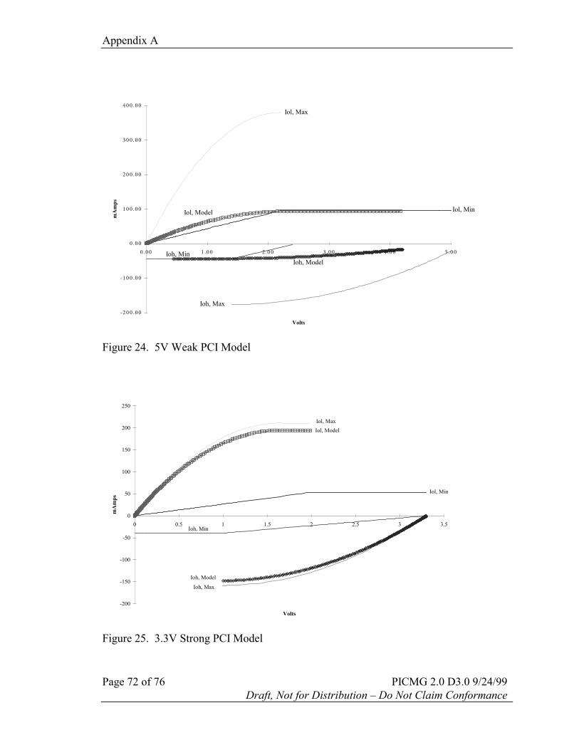
Appendix A
Page 72 of 76 PICMG 2.0 D3.0 9/24/99Draft, Not for Distribution – Do Not Claim Conformance
-200 .00
-100 .00
0.00
100.00
200.00
300.00
400.00
0.00 1.00 2.00 3 .00 4 .00 5 .00
Volts
mA
mps
Iol, Max
Ioh, Max
Iol, Min
Ioh, MinIoh, Model
Iol, Model
Figure 24. 5V Weak PCI Model
-200
-150
-100
-50
0
50
100
150
200
250
0 0.5 1 1.5 2 2.5 3 3.5
Volts
mA
mps
Iol, Max
Ioh, Max
Iol, Min
Ioh, Min
Ioh, Model
Iol, Model
Figure 25. 3.3V Strong PCI Model

Appendix A
CompactPCI® Core Specification PICMG 2.0 D3.0 9/24/99 Page 73 of 76Draft for PICMG Executive BallotDo not specify or claim conformance to this specification - Not for Distribution
-200
-150
-100
-50
0
50
100
150
200
250
0 0.5 1 1.5 2 2.5 3 3.5
Volts
mA
mps
Iol, Max
Ioh, Max
Iol, Min
Ioh, MinIoh, Model
Iol, Model
Figure 26. 3.3V Weak PCI Model


Appendix B
CompactPCI® Core Specification PICMG 2.0 D3.0 9/24/99 Page 75 of 76Draft for PICMG Executive BallotDo not specify or claim conformance to this specification - Not for Distribution
B. Connector Implementation
B.1 GeneralThis appendix provides more descriptive information on the use of 2mmconnectors including backward compatibility issues. The accompanying PICMGType AB 2mm Connector Guideline Document provides specification informationon the Type AB shroud in advance of an approved IEC specification. Once an IECspecification is available the Guideline Document shall be superceded.
B.2 ConnectorsWhen the CompactPCI pinout was originally defined using the IEC-61076-4-101family of connectors, there was a dilemma. In a 3U form-factor, only 47 rows ofpins would fit mechanically in the 100 mm board dimension, with allowancemade for the card guides. The original CompactPCI “J1” connector consisted of asingle piece "A" module, now designated J1, and a separate “B” module which isnow designated as J2. Simple 32-bit boards could be developed populated withonly the A module for cost savings.
This left the "B" module, as the logical connector to cut down by three rows tocreate the 47 row pair. Because of the way that the J2 connector had to be cutdown, rows 1-3 had to be removed because the mating surface between J1 and J2is keyed to prevent connectors from being inserted 180 degrees from one another.This would have left the connector starting at row 4.
To address this problem a decision was made to number connector pins frombottom to top, in the reverse order from IEC 61076-4-101.
It should be noted that the reversal in numbering is not, strictly speaking, on a pinfor pin basis. Therefore the pins are numbered from 1 at the bottom of J1P1 to 25at the top with three numbered positions in the middle that are taken up by thealignment and keying area. J2/P2 connector is numbered from the bottom to top 1through 22 in an uninterrupted pattern. The column designations, z, a, b, c, d, e,and f used by CompactPCI are unchanged and conform to IEC 61076-4-101.
B.3 Alignment
B.3.1 Front Plug-In Board AlignmentFront plug-in boards have alignment features on the Type A connectors to insurethe board mates correctly with the backplane. These are used in locations J1/P1and J4/P4.

Appendix B
Page 76 of 76 PICMG 2.0 D3.0 9/24/99Draft, Not for Distribution – Do Not Claim Conformance
B.3.2 Rear Panel I/O Board AlignmentDue to the connector population options on rear panel I/O boards for variousplatform options, all connectors used in the transition area shall have alignmentfeatures to insure the board mates correctly to the backplane. This is achievedthrough the use of Type A and Type AB connectors on the rear panel I/O boardsand backplane in locations shown in Figure 21 and Figure 22.
B.3.3 Backward Compatibility for Rear Panel I/O BoardsLegacy rear panel I/O boards based on the connector implementation forRevision 2.X and below of the CompactPCI specification will plug into systemsthat follow the connector implementation for Revision 3.X and above of theCompactPCI specification. However, rear panel I/O boards based on theconnector implementation for Revision 3.X and above of the CompactPCIspecification will not plug into the systems that follow the connectorimplementation for Revision 2.X and below of the CompactPCI specification.
This occurs due to a compatibility issue between Type B and Type ABconnectors required. In Revision 3.X and above of the CompactPCISpecification, Type AB connectors are specified in the rP2/rP3/rP5 andrJ2/rJ3/rJ5 locations to insure that any combination of connectors used for rearpanel I/O always have an alignment feature. In Revision 2.X and below, Type Bconnectors were specified in the rP2/rP3/rP5 and rJ2/rJ3/rJ5 locations. TypeABshrouds are backwards compatible with Type B right angle receptacles. Theconverse is not true. Type B shrouds are not backward compatible with TypeAB right angle receptacles.
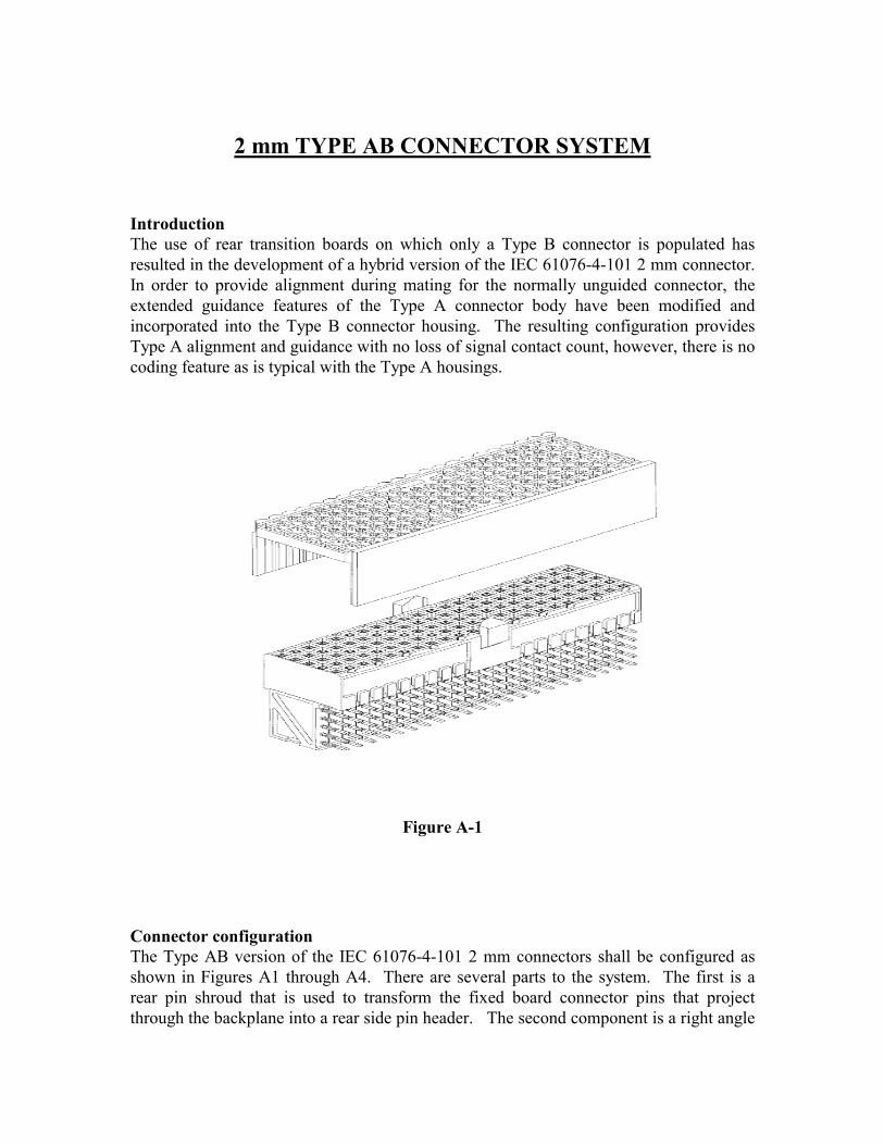
2 mm TYPE AB CONNECTOR SYSTEM
IntroductionThe use of rear transition boards on which only a Type B connector is populated hasresulted in the development of a hybrid version of the IEC 61076-4-101 2 mm connector.In order to provide alignment during mating for the normally unguided connector, theextended guidance features of the Type A connector body have been modified andincorporated into the Type B connector housing. The resulting configuration providesType A alignment and guidance with no loss of signal contact count, however, there is nocoding feature as is typical with the Type A housings.
Figure A-1
Connector configurationThe Type AB version of the IEC 61076-4-101 2 mm connectors shall be configured asshown in Figures A1 through A4. There are several parts to the system. The first is arear pin shroud that is used to transform the fixed board connector pins that projectthrough the backplane into a rear side pin header. The second component is a right angle

free board connector designed to mate with the Type AB shroud/pin combination. Thethird is a pre-assembled fixed board connector (pin header).
The Type AB extended guidance feature is similar to that found on the Type A version ofthe IEC 61076-4-101 connectors. It is designed to provide premating guidance andalignment for rear transition modules, especially those which have only the Type Bconnectors. The feature can also be successfully used to provide guidance for reartransition modules which have additional connectors, even those which have Type Aguidance/keying modules.
Connector namingThe proposed naming convention for the new connector will be Type AB. This is acombination of the Type A and B naming conventions utilized and already defined in theIEC 61076-4-101 specification. The new “family” of connectors will have threecomponents, excluding variations on shields, number of rows, pin lengths, etc. These are:
• Type AB shroud (19, 22 and 25 x 7 positions)• Type AB pin header (19, 22 and 25 x 7 positions)• Type AB right angle receptacle (free board) connector (19, 22 and 25 X 7
positions)
Recommended Method of MountingThe Type AB connector components are mounted in the same manner as other IEC61076-4-101 connectors. Shrouds must be supported and dimensionally located inaccordance with the rear transition module system defined in the IEEE 1101.11equipment practice.
Ratings and characteristicsAll ratings and characteristics shall be in accordance with IEC 61976-4-101.
Technical dataAll definitions, styles and variants and application information shall be in accordancewith IEC 61076-4-101 except as shown in figures A2 through A4.
Dimensional informationThe Type AB shroud, pin header and receptacle connector design details are shown inFigures A2 through A4. All dimensions not affected by the incorporation of the Type Aalignment features on the Type B connector bodies are controlled by the IEC 61076-4-101 standard.
Mating information It shall be possible to mate a Type B receptacle (free board) connector to a Type ABshroud/pin assembly or pin header (fixed board) connector. Type A receptacle (freeboard) connectors will not mate with Type AB shroud/pin or pin header assemblies.Mating misalignment tolerances shall be in accordance with IEC 61076-4-101.

AccessoriesCoding devices cannot be used with the Type AB versions of the IEC 61076-4-101connectors.
Electrical characteristicsAll electrical characteristics (creepage and clearance, voltage proof, current carryingcapacity, contact resistance and insulation resistance) shall be in accordance with IEC61076-4-101.
Mechanical characteristicsAll mechanical characteristics (mechanical operation, engaging and separating forces,contact retention, transverse static load, gage retention force, vibration, shock, andpolarizing method) shall be in accordance with IEC 61076-4-101.
Application ToolingTooling designed for the application of Type A receptacle (free board) connectors can beused to apply Type AB receptacle connectors. Tooling for the Type B receptacleconnectors can be used if the design includes a relieved section that provides clearancefor the guidance feature on the Type AB connector housing. Some manufacturers provideonly one receptacle tooling design (for the Type A) that is used on both the Type A and Breceptacle connectors. This can be used to apply the Type AB receptacle connectors toprinted boards.Tooling to press Type AB pin header assemblies onto printed boards differs from thatused for both the Type A and Type B pin headers, and tooling designed for the Types Aand B pin headers may not function in the Type AB pin headers. In Type AB tooling,provision is required to press contacts into the board in the area that would be reservedfor keying in the Type A connectors, allowance must be made to provide clearance for theguidance feature on the outer connector housing walls.
Test schedulesAll test schedules shall be in accordance with the applicable sections of IEC 61076-4-101.
Quality assessment proceduresQuality assessment procedures shall be in accordance with IEC 61076-4-101.

Figure A-2Shroud

Figure A-3Receptacle

Figure A-4A-B Pin