pci-pci bridge board specification for single board computer … · 3 1. preface 1.1 purpose and...
TRANSCRIPT
PICMG™ name and logo are trademarks of the PCI Industrial Computer Manufacturers Group
PCI-PCI BRIDGE BOARD SPECIFICATION FOR SINGLE BOARD COMPUTER (SBC)
Revision Number 1.02
Revision Date : August 01, 1995
PICMG™ name and logo are trademarks of the PCI Industrial Computer Manufacturers Group
Table Of Contents
1. Preface .................................................................................................................................... 3
1.1 Purpose and Terminology...................................................................................................3 1.2 Related Documents .............................................................................................................4 1.3 Trademarks ...........................................................................................................................4
2. PPBB Features ....................................................................................................................... 5
2.1 Number of PPBB Slots ........................................................................................................5
3. PPBB Signals.......................................................................................................................... 5
3.1 Primary Interface (PI) ...........................................................................................................5 3.1.1 Standard Primary Interface (SPI) ...............................................................................5 3.1.2 Connectivity of SPI ......................................................................................................6
3.2 Secondary Interface (SI) .....................................................................................................6 3.2.1 Support of PCI Expansion Slots on Secondary Interface ......................................6 3.2.2 Number of Secondary PCI Bus Expansion Slots .....................................................6 3.2.3 Connectivity ..................................................................................................................6 3.2.4 IDSEL Signal Assignation.............................................................................................7 3.2.5 Master Support .............................................................................................................7 3.2.6 Point to Point Signal Binding on Secondary Bus ....................................................7 3.2.7 S_ACK64# and S_REQ64# Signals ............................................................................8 3.2.8 Interrupt Binding on Secondary Bus .........................................................................8
4. Board Pin Assignment .......................................................................................................10
5. Backplane Layout ..............................................................................................................15
6. Extended Primary Interface (EPI) ....................................................................................15
6.1 Difference Between EPI and SI .......................................................................................15 6.2 Difference Between EPI and PCI PICMG Bus ..............................................................15
7. Connection of EPI to PCI-ISA Bus on Backplane .......................................................15
8. Physical Characteristics ...................................................................................................16
Figure 1 : 32-Bit PPBB Card Figure 2 : 64-Bit PPBB Card Figure 3 : Typical PCI-PCI Bridge Board Figure 4 : Host PCI Board Drives 7 PCI Slots Figure 5 : Host PCI Board with Onboard PCI Devices Drives 7 PCI Slots

3
1. Preface
1.1 Purpose and Terminology To standardize the hardware interface of peripherals that integrate PCI to PCI Bridge for use in passive backplane environment. The primary goal of this proposal is to define a common set of electrical and mechanical interfaces that allows System Designers to add more PCI expansion slots to passive backplanes using a PCI to PCI bridge board. However, it does not preclude designs that integrate the bridge directly onto the backplane. . PPBB PCI to PCI Bridge Board. An architectural, electrical, and physical interface that allows System Designers to add more PCI expansion slots on passive backplane environment. The specification of PPBB is the subject of this document. . PCI System Controller PCI device that assumes central resource functions. These functions include the following: - Central arbitration - Required signal pullups - Generation of IDSEL signals for system configuration - Generation of system clock - Generation of system reset signal. Host bridge, standard bus bridge, and secondary side of a PCI to PCI bridge are candidates for the PCI system controller. . PICMG PCI Bus A modified version of PCI Bus for Industrial Single Board Computer and Backplane designers, developed by the PICMG consortium. The PICMG PCI bus is based on PCI Local Bus. Pinout and functions have been modified to allow PCI system controller located on PICMG bus to monitor PCI expansion slots on passive backplane. . Primary PCI Bus Interface The standard PCI Interface that interacts with the bus closest to bus 0 (CPU).

4
. Secondary PCI Bus Interface The standard PCI interface of the PPBB that is connected to the PCI bus farthest from bus 0. In addition, the secondary interface implements PCI’s system controller functions. . Interrupt Handler The modules that have interrupt controllers integrated. . Arbiter The modules that have the capability of monitoring bus requests and grants control (modules that have central arbitration function integrated). . System Clock Driver The modules that provide PCI compliance clock signals to PCI devices and expansion slots. . Power Monitor The module with the capability of generating PCI bus reset# signal.
1.2 Related Documents The following documents may be useful references while reading this document: PCI Local Bus, Revision 2.0 PCI BIOS ROM Specification, Revision 2.1 PCI to PCI Bridge Architecture Specification, Revision 1.0 PCI System Design Guide, Revision 1.0 PCI-ISA Card Edge Connector Revision 2.0 1.3 Trademarks The trademarks mentioned in this document are the property of their respective owners.
5
2. PPBB Features The PPBB architecture was designed to be easily adapted to the design of systems running on backplanes compatible with PCI-ISA specification rev 2.0. The PPBB follows PCI to PCI Bridge Architecture Specification rev 1.0.
2.1 Number of PPBB Slots A design may consist of zero to four PPBB slots. These slots are supported by PCI-ISA bus defined by PCI-ISA card edge connector proposal for SBC rev 2.0. The number of PPBB slots may be limited to fewer than four depending on the loading on the bus and the spacing of these connectors on the backplane. The implementation must be analyzed and tested to ensure that the timing meets PCI specifications. The four PPBBs are organized as peers. More PPBBs can be added using a hierarchical organization. The four PPBB slots (connectors) are named as follows: PPBB slot 1 : Connector next to PCI-ISA slot PPBB slot 2 : Connector next to PPBB slot 1 PPBB slot 3 : Connector next to PPBB slot 2 PPBB slot 4 : Connector next to PPBB slot 3
3. PPBB Signals The PPBB has two forms: standard 32-bit and 64-bit extension. The standard 32-bit extension contains 248 logical pins. The 64-bit extension extends the total number of pins to 376 logical pins. PPBB has two set of signals named Primary Interface (PI) and Secondary Interface (SI). The Primary Interface is connected to Primary PCI Bus, and the Secondary Interface is connected to Secondary PCI Bus. 3.1 Primary Interface (PI) The PI is designed to interact with PCI Bus closest to Bus 0. The function of PI is compliant with Primary Interface defined in PCI to PCI Bridge Architecture Spec. Rev 1.0. Two forms have been developed: Standard Primary Interface and Extended Primary Interface. 3.1.1 Standard Primary Interface (SPI) The Standard Primary Interface contains all signals defined by PCI Specification rev 2.0, and is connected to the PCI bus closest to the PCI Bus 0 (CPU). The two signals “PRSNT#s” are not supported and the two related pins are defined as “Reserved.” SPI is useful for modules that integrate simple PCI to PCI bridge devices.
6
3.1.2 Connectivity of SPI The four PPBB primary interfaces are connected to PCI-ISA Bus following the rules specified in section 8 of PCI-ISA Card Edge Connector Proposal rev 2.0. PPBB slot 1 is equivalent to PCI slot 1 PPBB slot 2 is equivalent to PCI slot 2 PPBB slot 3 is equivalent to PCI slot 3 PPBB slot 4 is equivalent to PCI slot 4 To support PPBB’s Primary interface in mode extended (refer to chapter 6), the clock input of PPBB slot 1 (pin D16) is driven by PCI-ISA bus clock CLKB (pin F16), and the PPBB slot 2 clock input (pin D16) is driven by PCI-ISA bus clock CLKA (pin F14). 3.2 Secondary Interface (SI) Secondary Interface consists of standard set of PICMG PCI signals and is connected to the PCI bus farthest from Bus 0. The functions of SI are compliant with the Secondary Interface defined in PCI to PCI Bridge Architecture Spec. Rev 1.0. 3.2.1 Support of PCI Expansion Slots on Secondary Interface The PPBB Secondary Interface consists of standard set of PICMG PCI signals, and is used to support PCI expansion slots mounted on passive backplane. The Interface supports all functions defined for PCI to PCI Bridge’s Secondary Interface. PPBB Secondary Interface must support PCI system controller functions including: Interrupt Handler, Central Arbitration, System Clock Driver, and Power Monitor. Bus parking on PPBB modules is optional. 3.2.2 Number of Secondary PCI Bus Expansion Slots Each PPBB is capable of supporting zero to four secondary PCI bus slots through its Secondary Interface. These slots can be masters or slaves. 3.2.3 Connectivity The four Secondary PCI slots (connectors) are named as follows: S_PCI slot 1 : Connector immediately next to PPBB connector S_PCI slot 2 : Connector next to S_PCI slot 1 S_PCI slot 3 : Connector next to S_PCI slot 2 S_PCI slot 4 : Connector next to S_PCI slot 3 (the farthest from PPBC connector) PPBB may support fewer than four S_PCI connectors. In this case, the S_PCI connectors should be configured starting from S_PCI connector 1.

7
3.2.4 IDSEL Signal Assignation S_ADxx lines S_AD31 down to S_AD28 are used to support S_IDSEL signals on backplane’s Secondary PCI expansion slots. Routing of S_ADxx lines to S_IDSEL lines is done on backplane. 3.2.5 Master Support The PPBB is designed to support up to four secondary slots with master capabilities. If a PPBB does not support all four S_PCI connectors or four S_PCI connectors in master mode, it must support S_PCI connectors, starting from 1 then 2, 3, 4 respectively. For example, if a PPBB board has the capability of supporting two S_PCI connectors but only one can be in master, it should be configured to support S_PCI connector 1 in master and S_PCI connector 2 in slave mode. 3.2.6 Point to Point Signal Binding on Secondary Bus The Point to Point signals binding scheme on Secondary PCI bus follows PCI-ISA specification rev 2.0. The table below summarizes Point to Point signal connection from PPBB secondary interface connector to Secondary PCI expansion connectors. S_PCI Connector 1 PPBB Secondary Interface Signal Pin Signal Pin REQ# B18 S_REQ0# B18 GNT# A17 S_GNT0# A17 CLK B16 S_CLKA B14 IDSEL A26 S_AD31 B20 S_PCI Connector 2 PPBB Secondary Interface Signal Pin Signal Pin REQ# B18 S_REQ1# B10 GNT# A17 S_GNT1# A14 CLK B16 S_CLKB B16 IDSEL A26 S_AD30 A20

8
S_PCI Connector 3 PPBB Secondary Interface Signal Pin Signal Pin REQ# B18 S_REQ2# A19 GNT# A17 S_GNT2# A26 CLK B16 S_CLKC A09 IDSEL A26 S_AD29 B21 S_PCI Connector 4 PPBB Secondary Interface Signal Pin Signal Pin REQ# B18 S_REQ3# B09 GNT# A17 S_GNT3# B11 CLK B16 S_CLKD A11 IDSEL A26 S_AD28 A22
3.2.7 S_ACK64# and S_REQ64# Signals To support both 32-bit and 64-bit PCI standard, the 2 signals REQ64# and ACK64# of each Secondary PCI expansion slot are pulled-up on the backplane by 2 resistors (one for REQ64# and one for ACK64#) for 32-bit version. For 64-bit version, the signals REQ#64 and ACK64# are bussed together and pulled-up with a single resistor on each signal on the backplane. If the PPBB supports 64-bit version, the signals S_REQ64# and S_ACK64# should be connected to REQ64# and ACK64# of the 64-bit Secondary Expansion Slots. These signals are bussed together and pulled-up with a single resistor on each signal on the backplane. Pullup resistors should be connected to the +V I/O plane to support both +5V and 3.3V environment.
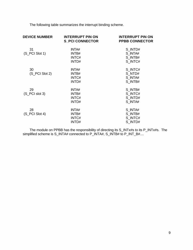
3.2.8 Interrupt Binding on Secondary Bus The Interrupt Binding Scheme on the backplane for a Secondary PCI bus follows PCI to PCI Bridge Specification rev 1.0.
9
The following table summarizes the interrupt binding scheme. DEVICE NUMBER INTERRUPT PIN ON INTERRUPT PIN ON S_PCI CONNECTOR PPBB CONNECTOR 31 INTA# S_INTD# (S_PCI Slot 1) INTB# S_INTA# INTC# S_INTB# INTD# S_INTC# 30 INTA# S_INTC# (S_PCI Slot 2) INTB# S_NTD# INTC# S_INTA# INTD# S_INTB# 29 INTA# S_INTB# (S_PCI slot 3) INTB# S_INTC# INTC# S_INTD# INTD# S_INTA# 28 INTA# S_INTA# (S_PCI Slot 4) INTB# S_INTB# INTC# S_INTC# INTD# S_INTD# The module on PPBB has the responsibility of directing its S_INTx#s to its P_INTx#s. The simplified scheme is S_INTA# connected to P_INTA#, S_INTB# to P_INT_B#....
10
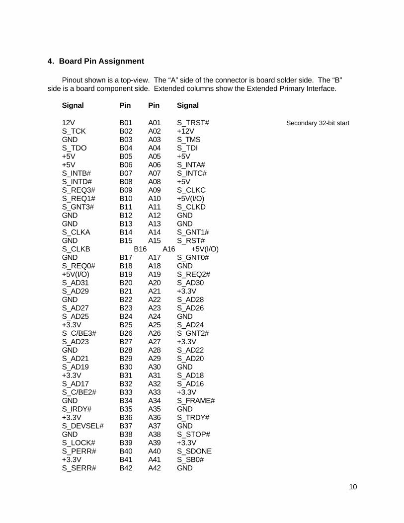
4. Board Pin Assignment Pinout shown is a top-view. The “A” side of the connector is board solder side. The “B” side is a board component side. Extended columns show the Extended Primary Interface. Signal Pin Pin Signal 12V B01 A01 S_TRST# Secondary 32-bit start S_TCK B02 A02 +12V GND B03 A03 S_TMS S_TDO B04 A04 S_TDI +5V B05 A05 +5V +5V B06 A06 S_INTA# S_INTB# B07 A07 S_INTC# S_INTD# B08 A08 +5V S_REQ3# B09 A09 S_CLKC S_REQ1# B10 A10 +5V(I/O) S_GNT3# B11 A11 S_CLKD GND B12 A12 GND GND B13 A13 GND S_CLKA B14 A14 S_GNT1# GND B15 A15 S_RST# S_CLKB B16 A16 +5V(I/O) GND B17 A17 S_GNT0# S_REQ0# B18 A18 GND +5V(I/O) B19 A19 S_REQ2# S_AD31 B20 A20 S_AD30 S_AD29 B21 A21 +3.3V GND B22 A22 S_AD28 S_AD27 B23 A23 S_AD26 S_AD25 B24 A24 GND +3.3V B25 A25 S_AD24 S_C/BE3# B26 A26 S_GNT2# S_AD23 B27 A27 +3.3V GND B28 A28 S_AD22 S_AD21 B29 A29 S_AD20 S_AD19 B30 A30 GND +3.3V B31 A31 S_AD18 S_AD17 B32 A32 S_AD16 S_C/BE2# B33 A33 +3.3V GND B34 A34 S_FRAME# S_IRDY# B35 A35 GND +3.3V B36 A36 S_TRDY# S_DEVSEL# B37 A37 GND GND B38 A38 S_STOP# S_LOCK# B39 A39 +3.3V S_PERR# B40 A40 S_SDONE +3.3V B41 A41 S_SB0# S_SERR# B42 A42 GND

11
+3.3V B43 A43 PAR S_C/BE1# B44 A44 S_AD15 S_AD14 B45 A45 +3.3V GND B46 A46 S_AD13 S_AD12 B47 A47 S_AD11 S_AD10 B48 A48 GND GND B49 A49 S_AD09 CONNECTOR KEY CONNECTOR KEY S_AD08 B52 A52 S_C/BE0# S_AD07 B53 A53 +3.3V +3.3V B54 A54 S_AD06 S_AD05 B55 A55 S_AD04 S_AD03 B56 A56 GND GND B57 A57 S_AD02 S_AD01 B58 A58 S_AD00 +5V(I/O) B59 A59 +5V(I/O) S_ACK64# B60 A60 S_REQ64# +5V B61 A61 +5V +5V B62 A62 +5V Secondary 32-bit end CONNECTOR KEY CONNECTOR KEY Secondary 64-bit start Reserved B63 A63 GND GND B64 A64 S_C/BE7# S_C/BE6# B65 A65 S_C/BE5# S_C/BE4# B66 A66 +5V(I/O) GND B67 A67 PAR64 S_AD63 B68 A68 S_AD62 S_AD61 B69 A69 GND +5V(I/O) B70 A70 S_AD60 S_AD59 B71 A71 S_AD58 S_AD57 B72 A72 GND GND B73 A73 S_AD56 S_AD55 B74 A74 S_AD54 S_AD53 B75 A75 +5V(I/O) GND B76 A76 S_AD52 S_AD51 B77 A77 S_AD50 S_AD49 B78 A78 GND +5V(I/O) B79 A79 S_AD48 S_AD47 B80 A80 S_AD46 S_AD45 B81 A81 GND GND B82 A82 S_AD44 S_AD43 B83 A83 S_AD42 S_AD41 B84 A84 +5V(I/O) GND B85 A85 S_AD40 S_AD39 B86 A86 S_AD38 S_AD37 B87 A87 GND +5V(I/O) B88 A88 S_AD36 S_AD35 B89 A89 S_AD34 S_AD33 B90 A90 GND

12
GND B91 A91 S_AD32 Reserved B92 A92 Reserved Reserved B93 A93 GND GND B94 A94 Reserved Secondary 64-bit end

13
Extended Signal Pin Pin Signal Extended 12V D01 C01 P_TRST# Primary 32-bit start P_TCK D02 C02 +12V GND D03 C03 P_TMS P_TDO D04 C04 P_TDI +5V D05 C05 +5V +5V D06 C06 P_INTA# P_INTB# D07 C07 P_INTC# P_INTD# D08 C08 +5V P_REQ3# Reserved D09 C09 Reserved P_CLKC# P_REQ#1 Reserved D10 C10 +5V(I/O) P_GNT3# Reserved D11 C11 Reserved P_CLKD# GND D12 C12 GND GND D13 C13 GND P_CLKA Reserved D14 C14 Reserved P_GNT1# GND D15 C15 P_RST# P_CLKB P_CLK D16 C16 +5V(I/O) GND D17 C17 GNT# P_GNT0# P_REQ0# REQ# D18 C18 GND +5V(I/O) D19 C19 Reserved P_REQ2# P_AD31 D20 C20 P_AD30 P_AD29 D21 C21 +3.3V GND D22 C22 P_AD28 P_AD27 D23 C23 P_AD26 P_AD25 D24 C24 GND +3.3V D25 C25 P_AD24 P_C/BE3# D26 C26 IDSEL P_GNT2# P_AD23 D27 C27 +3.3V GND D28 C28 P_AD22 P_AD21 D29 C29 P_AD20 P_AD19 D30 C30 GND +3.3V D31 C31 P_AD18 P_AD17 D32 C32 P_AD16 P_C/BE2# D33 C32 +3.3V PND D34 C34 P_FRAME# P_IRDY# D35 C35 GND +3.3V D36 C36 P_TRDY# P_DEVSEL# D37 C37 GND GND D38 C38 P_STOP# P_LOCK# D39 C39 +3.3V P_PERR# D40 C40 P_SDONE 3.3V D41 C41 P_SB0# P_SERR# D42 C42 GND +3.3V D43 C43 P_PAR P_C/BE1# D44 C44 P_AD15 P_AD14 D45 C45 +3.3V GND D46 C46 P_AD13 P_AD12 D47 C47 P_AD11 P_AD10 D48 C48 GND

14
GND D49 C49 P_AD09 CONNECTOR KEY CONNECTOR KEY P_AD08 D52 C52 P_C/BE0# P_AD07 D53 C53 +3.3V +3.3V D54 C54 P_AD06 P_AD05 D55 C55 P_AD04 P_AD03 D56 C56 GND GND D57 C57 P_AD02 P_AD01 D58 C58 P_AD00 +5V(I/O) D59 C59 +5V(I/O) P_ACK64# D60 C60 P_REQ64# +5V D61 C61 +5V +5V D62 C62 +5V Primary 32-bit end CONNECTOR KEY CONNECTOR KEY Reserved D63 C63 GND Primary 64-bit start GND D64 C64 P_C/BE7# P_C/BE6# D65 C65 P_C/BE5# P_C/BE4# D66 C66 +5V(I/O) GND D67 C67 P_PAR64 P_AD63 D68 C68 P_AD62 P_AD61 D69 C69 GND +5V(I/O) D70 C70 P_AD60 AD59 D71 C71 P_AD58 P_AD57 D72 C72 GND GND D73 C73 P_AD56 P_AD55 D74 C74 P_AD54 P_AD53 D75 C75 +5V(I/O) GND D76 C76 P_AD52 P_AD51 D77 C77 P_AD50 P_AD49 D78 C78 GND +5V(I/O) D79 C79 P_AD48 P_AD47 D80 C80 P_AD46 P_AD45 D81 C81 GND GND D82 C82 P_AD44 P_AD43 D83 C83 P_AD42 P_AD41 D84 C84 +5V(I/O) GND D85 C85 P_AD40 P_AD39 D86 C86 P_AD38 P_AD37 D87 C87 GND +5V(I/O) D88 C88 P_AD36 P_AD35 D89 C89 P_AD34 P_AD33 D90 C90 GND GND D91 C91 P_AD32 Reserved D92 C92 Reserved Reserved D93 C93 GND GND D94 C94 Reserved
15
5. Backplane Layout Figures 3 and 4 show examples of connector layout on passive backplanes. A maximum of four PPBB can be added, allowing expansion of up to four PCI buses in peer organization. The PCI-ISA connector supports CPU board with host bridge integrated (Bus 0). Four PPBB primary interfaces connected to Bus 0 with PPBB slot 1 next to PCI-ISA slot. 6. Extended Primary Interface (EPI) PPBB slot 1 can be designed to support either standard PPBB modules or PPBB modules that have the capability of assuming system controller functions on both interfaces (Primary and Secondary). EPI is a variation of the Secondary Interface to allow support of functions mentioned above. In the absence of CPU board resident in the PCI-ISA slot, a special PPBB module located on PPBB slot 1 can monitor PCI buses resident in the backplane. 6.1 Difference Between EPI and SI -- EPI connects to PCI bus 0 or closest to bus 0 in slot 1. -- EPI supports primary interface functions defined in PCI to PCI Bridge Architecture Spec. rev 2.0. 6.2 Difference Between EPI and PCI PICMG Bus -- EPI supports a maximum of three master capable PCI expansion slots (2, 3, and 4 only). -- EPI pin P_CLKA (F14) drives PCI expansion slot 2’s clock input. -- EPI pin P_CLKB(F!6) drives onboard PCI-to_PCI bridge, and is connected to PCI-ISA bus pin CLKB(F16). -- PCI Primary connector 2’s clock input (B16) is driven by PCI-ISA bus pin CLKA (F14) 7. Connection of EPI to PCI-ISA Bus on Backplane The extended pins (refer to board pin assignment section, extended columns ) P_REQ(0,1,3)# and P_GNT(0,1,2,3)# are connected to PCI-ISA bus REQ(0,1,3)# and GNT(0,1,2,3)# pins respectively. Pin C26 has two functions that depend on mode setting. In SPI mode, this pin is configured as IDSEL input signal and is connected to the address line AD31. In EPI mode, this pin becomes P_GNT2# output signal and drives GNT2# to PCI slot 3. A jumper (or a switch) should be added on backplane to allow configuration of the slot. Pin P_CLK (D16) is connected to PCI-ISA Bus pin CLKB (F16). The Pin P_CLKA (F16) should be connected to CLKA (F14) of the PCI-ISA bus.

16
The table below summarizes connections of PCI-ISA bus to PPBB slot 1. PCI-ISA Connector PPBB Connector
Signal Pin Signal Pin INTA# E06 P_INTD# D08 INTB# F07 P_INTA# C06 INTC# E07 P_INTB# D07 INTD# F08 P_INTC# C07 CLKA F14 P_CLKA D14 CLKB F16 P_CLKB D16 CLKC E09 P_CLKC C09 CLKD E11 P_CLKD C11 REQ0# F18 P_REQ# D18 GNT0# E17 P_GNT# C17 REQ1# F10 P_REQ1# D10 GNT1# E14 P_GNT1# C14 REQ2# E19 P_REQ2# C19 GNT2# E26 P_GNT2# C26 (jumper) REQ3# F09 P_REQ3# D09 GNT3# F11 P_GNT3# D11 AD31 F20 IDSEL C26 (jumper) 8. Physical Characteristics The PPBC Bus slot is defined as two PCI Bus connectors. One is in line with the other. The secondary interface connector is placed close to the bracket end followed by the primary interface connector. Pin 1 of the primary interface connector is 5.102 inches (pin center) from pin 1 of the secondary interface connector. This layout allows both 32-bit and 64-bit versions to be physically compatible. Also it allows ease to lay out primary and secondary interface. The component side of PPBB card is the opposite of ISA cards. The card dimensions follow PCI specification rev 2.0.

17
Secondary InterfacePrimary Interface
MAX
32-bit32-bit
A
Figure 1 : 32-BIT PPBB CARD
3.522
4.113
4.
20
0
0.612
SOLDER SIDE6.740
12.283
5.102

18
MAX
A
64-bitSecondary Interface64-bit
Primary Interface
Figure 2 : 64-BIT PPBB CARD
5.102
4.113
3.522
4.
20
0
SOLDER SIDE
0.612
12.283

19
Figure 3: Typical PCI-PCI Bridge Board
CONTROL
ROUTING
INTERRUPTS
BUFFER
CLOCK
DRIVEN BY PCI-ISA SLOT
PRIMARY INTERFACE
DRIVES FOUR EXPANSION SLOTS ON BUS 1
SECONDARY INTERFACE
BRIDGE
PCI to PCI

20
Figure 4: Host PCI Board Drives 7 PCI Slots
DRIVES FOUR EXPANSION SLOTS ON BUS 1DRIVES THREE PCI SLOTS ON BUS 0
SECONDARY INTERFACEEXTENDED PRIMARY INTERFACE
BUS 0
BRIDGE
PCI to PCI
BRIDGEHOST
CPU

21
Figure 5: Host PCI Board with Onboard PCI Devices Drives 7 PCI Slots
DEVICE DEVICE DEVICEPCI PCI PCI
DRIVES FOUR EXPANSION SLOTS ON BUS 1DRIVES THREE PCI SLOTS ON BUS 0
SECONDARY INTERFACEEXTENDED PRIMARY INTERFACE
BUS 0
BRIDGEBRIDGEPCI to PCIPCI to PCI
BRIDGEHOST
CPU