pcii-629 datasheet 7-12-2007
TRANSCRIPT

PCI-629™ ARINC-629 Tester Card
CORELIS
• Connects to one of four multiplexed ARINC-629 Channels at a time
• Intelligent PCI card with on-board autonomous processor
• The selected channel can send/receive simultaneously at top speed
• Multiple Terminal Emulation capabilities, up to 120 Terminals
• Extensive ARINC-629 bus error injection and detection capability
• Programmable Traffic Generator mode can transmit arbitrary ARINC-629 data, including user injected intentional errors
• On-board 4 MByte Shared Memory • Flexible Traffic Collection Buffering
Accessible in Real-time • High-performance interface
between a host PC and ARINC-629 bus
• Pseudo Bus (TTL) or SIM Bus (via external CMC to ARINC-629 twisted-pair) interfaces supported - software selected
• Programmable 8 bit general purpose parallel I/O signals
• Windows GUI and Console Demo Software Provided
• Host Software Support With Extensive “C” Library Calls and Utilities
Overview The PCI-629 is an intelligent single-slot PCI module providing broad ARINC-629 bus testing capabilities. These include monitoring traffic, multiple terminal emulation, and fault insertion/detection. The ARINC-629 test channel is soft-ware switch-able to one of four ARINC-629 bus interfaces at the front panel. Pseudo Bus (TTL) sig-naling is also supported as well as the avionics SIM Bus (external CMC with ARINC-629 twisted pair re-quired). An embedded Boeing approved Data Terminal (DATAC) device sup-ports these modes; Periodic, Aperi-odic, C, Block, Alternate, and Inde-pendent. The host PC thus has full traffic access, switchable between four ARINC-629 busses. Also, the card can simulate up to 120 concurrent terminals, useful for traffic simulation, fault insertion, and bus stressing. Traffic can be filtered and buffered using various storage schemes. The host can extract this during runtime, enabling an endless collec-tion of bus activity.
PCI-629 Architecture
Figure 1 shows a simplified high level block diagram of the PCI-629 and its interface groups. Table 1
provides a brief description of each interface . All but the PCI interface are wired to the front-panel 68 pin SCSI-II type connector. The PCI signals connect at the standard PC socket fingers ready for adapter plug-in. Figure 2 depicts the SCSI-II type I/O connector and its pin assignments, with Table 2 identifying its signals.
Feature Details The PCI-629 is a complete ARINC-629 Tester on a single PCI bus plug-in card. It is specially designed for testing and simulation of ARINC-629 communication interfaces and is an ideal solution for design engi-neers, manufacturing testers, simu-lation labs, and field maintenance facilities. The PCI-629 incorporates many hardware and firmware fea-tures that make it both easy to use and yet highly programmable and flexible. The following is a list of some of the special features of this module: • Full ARINC-629 bus monitoring
capability, including features that are not available with the standard Boeing DATAC chip such as receiving all Label words including messages sent by the card itself.
• All received messages are time
tagged with a 40-bit time stamp with 0.5 μsec resolution. The user can record the data in
Applications • Avionics LRU/SRU Qualification
▪ Observe Bus Interactions ▪ High Traffic Stress Test ▪ Bus Access for SOFT-
WARE Simulation • System Integration
▪ Live Environment Simula-tion
▪ Characterize Performance ▪ Bus Infrastructure Network
Qualification • Factory Acceptance Testing
▪ Operational Validation ▪ Test/Burn-in Cycling
• Field Support ▪ Re-confirm Unit Behavior ▪ Test Upgrades ▪ Debug Failed Units
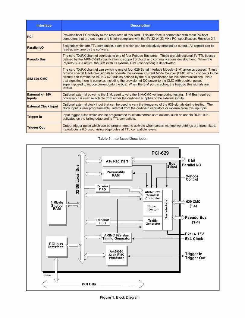
Interface Description
PCI Provides host PC visibility to the resources of this card. This interface is compatible with most PC host computers that are out there and is fully compliant with the 5V 32-bit 33 MHz PCI specification, Revision 2.1.
Parallel I/O 8 signals which are TTL compatible, each of which can be selectively enabled as output. All signals can be read at any time by the software.
Pseudo Bus The card TX/RX channel connects to one of four Pseudo Bus ports. These are bidirectional 5V TTL busses defined by the ARINC-629 specification to support protocol and communications development. When the Pseudo Bus is active, the SIM (with its external CMC connection) is deactivated.
SIM 629-CMC
The card TX/RX channel can switch to one of four 629 Serial Interface Module (SIM) avionics busses. These provide special full-duplex signals to operate the external Current Mode Coupler (CMC) which connects to the twisted-pair terminated ARINC-629 bus as defined by the bus specification for live communications. Note that signaling here is complex, including the provision of DC power to the CMC with doublet pulses superimposed to induce current onto the bus. When the SIM port is active, the Pseudo Bus signals are invalid.
External +/- 15V Inputs
Optional external power to the SIM, used to vary the SIM/CMC voltage during testing. SIM Bus required power input is user selectable from either the on-board supplies or the external inputs.
External Clock Input Optional external clock input that can be used to vary the frequency of the 629 signals during testing. The clock input is user programmable: internal from the on-board oscillators or external from this input pin.
Trigger In Input trigger pulse which can be programmed to initiate certain card actions, such as enable RUN. It is activated on the falling edge and is TTL compatible.
Trigger Out Output trigger pulse which can be programmed to activate when certain marked wordstrings are transmitted. It produces a 0.5 usec. rising edge pulse at TTL compatible levels.
Table 1. Interfaces Description
Figure 1. Block Diagram

Figure 2. PCI-629 64-pin TAP Connector Pinout
control the 629 bus bit stream directly via the Traffic generator mode.
• Intelligent card with on-board
RISC CPU can perform 629 communication tasks autono-mously without host interven-tion freeing it up for other activ-ity.
• Bit and word level error injec-
tion features are host program-mable on a word-by-word ba-sis. Message and protocol level errors can easily be created. The user can arbitrarily decide where and when to inject errors with many variations.
• The 629 on-board channel can
be switched under software control to one of four 629 inter-faces. This simplifies the con-nection to multiple 629 buses as no external switching hard-ware is required.
• Both Pseudo Bus (Voltage mode) and SIM Bus (Current mode) 629 interfaces are imple-mented. Power to the external Current Mode Coupler (CMC) is provided by the PCI-629 card. If supported by the UUT, the Pseudo Bus interface can be used to connect directly to the UUT avoiding the expensive CMCs.
• Input and output triggers are
provided at the front panel con-nector of the card. This allows synchronization of the opera-tion of the PCI-629 to external instruments.
• A 629_UTIL software demo tool
operates the card with text file controlled traffic simulation via friendly GUI screens. Also, a simple console demo program is provided with source serving as a prototype user application starting point, including DLL driver calls.
• Flexible architecture can be
expanded to include future en-hancements.
General Description The PCI-629 is a PCI based ARINC-629 Bus Tester module that fits in a single 32-bit PCI slot of the host computer. It is designed to provide a wide range of features for testing and simulation applications of ARINC-629 compatible systems. The PCI-629 is specially designed to support multiple terminal emula-tion, monitoring of ARINC-629 bus traffic and fault insertion and detec-tion. The ability to emulate up to120 ARINC-629 data terminals in the normal periodic fashion is provided as well as arbitrary traffic generation and error injection. The terminal emulator can be pro-grammed to generate user defined ARINC-629 bus traffic operating in any one of five modes as follows: 1. Single Terminal and bus monitor 2. Multiple Terminal Emulator (MTE) 3. Traffic Generator mode 4. Multiple Terminal Emulator with error injection 5. Traffic Generator with error injec-tion
memory (which the host can pipe to an external hard disk) in real time for later reconstruction or replay.
• The shared memory on-board is 4 Mbyte, enough to support the most demanding applica-tions.
• Emulate up to 120 terminals on
the 629 bus, each independ-ently talking on the bus.
• Traffic generator mode is useful
for creating arbitrary traffic that does not have to conform to the 629 bus specification and/or limitations. Use it to test the TI, TG and SG timers on your tar-get system or to evaluate its response under extreme or faulty conditions.
• When emulating 120 terminals,
the user can either provide an XPP for each terminal or can

Table 2. Pin Descriptions
Group Signal Name Pin I/O Description Bus 1 RSB1 1 In ARINC 629 Bus Coupler Receive, B
RSA1 2 In ARINC 629 Bus Coupler Receive, A TSB1 4 Out ARINC 629 Bus Coupler Transmit, B TSA1 5 Out ARINC 629 Bus Coupler Transmit, A PSEUDO1_R1 6 - 60 ohm pull-up to +5V PSEUDO1_TXN* 7 I/O Pseudo Bus - Line 2 (open collector) PSEUDO1_TXO* 8 I/O Pseudo Bus - Line 1 (open collector) PSEUDO1_R2 9 - 60 ohm pull-up to +5V
Bus 2 RSB2 11 In ARINC 629 Bus Coupler Receive, B RSA2 12 In ARINC 629 Bus Coupler Receive, A TSB2 14 Out ARINC 629 Bus Coupler Transmit, B TSA2 15 Out ARINC 629 Bus Coupler Transmit, A PSEUDO2_R1 16 - 60 ohm pull-up to +5V PSEUDO2_TXN* 17 I/O Pseudo Bus - Line 2 (open collector) PSEUDO2_TXO* 18 I/O Pseudo Bus - Line 1 (open collector) PSEUDO2_R2 19 - 60 ohm pull-up to +5V
Bus 3 RSB3 21 In ARINC 629 Bus Coupler Receive, B RSA3 22 In ARINC 629 Bus Coupler Receive, A TSB3 24 Out ARINC 629 Bus Coupler Transmit, B TSA3 25 Out ARINC 629 Bus Coupler Transmit, A PSEUDO3_R1 26 - 60 ohm pull-up to +5V PSEUDO3_TXN* 27 I/O Pseudo Bus - Line 2 (open collector) PSEUDO3_TXO* 28 I/O Pseudo Bus - Line 1 (open collector) PSEUDO3_R2 29 - 60 ohm pull-up to +5V
Bus 4 RSB4 31 In ARINC 629 Bus Coupler Receive, B RSA4 32 In ARINC 629 Bus Coupler Receive, A TSB4 34 Out ARINC 629 Bus Coupler Transmit, B TSA4 35 Out ARINC 629 Bus Coupler Transmit, A PSEUDO4_R1 36 - 60 ohm pull-up to +5V PSEUDO4_TXN* 37 I/O Pseudo Bus - Line 2 (open collector) PSEUDO4_TXO* 38 I/O Pseudo Bus - Line 1 (open collector) PSEUDO4_R2 39 - 60 ohm pull-up to +5V
Triggers FP_TRGOUT 41 Out External Trigger Output FP_TRIGIN 42 In External Trigger Input
629 Sync EX_CMDP* 43 In C-Mode Pulse Input EX_MAFS* 45 In Major Frame Sync EX_MIFS* 46 In Minor Frame Sync EXT_CLK 47 In External Clock Input
Parallel I/O PIO0 49 I/O Parallel I/O 0 (LSB) PIO1 50 I/O Parallel I/O 1 PIO2 51 I/O Parallel I/O 2 PIO3 52 I/O Parallel I/O 3 PIO4 53 I/O Parallel I/O 4 PIO5 54 I/O Parallel I/O 5 PIO6 55 I/O Parallel I/O 6 PIO7 56 I/O Parallel I/O 7 (MSB)
Cable Sense SENSE* 58 In Target Cable Connected Sense External Pwr +15VEXT 67 In +15V SIM/CMC Power Input
-15VEXT 68 In -15V SIM/CMC Power Input

An on-board Boeing approved Data Terminal (DATAC) device is used for single terminal data transmission and reception. This is connected to a Boeing approved SIM device. The Transmit Personality PROM (XPP), Receive personality PROM (RPP) and Multiple personality PROM (MPP) for the DATAC chip are im-plemented using a host download-able static RAM device rather than the traditional ROM. A 128K x 8 SRAM chip provides four 8K byte XPP memories, one 32K byte RPP memory, and one 64K byte MPP memory for the ARINC-629 terminal. The memory content is similar to the standard 629 personality memories. The Multiple Data Terminal Emula-tor, error injector and Traffic Gen-erator logic is implemented with on-board field programmable gate ar-ray (FPGA) devices. The DATAC chip is bypassed by the logic so that the user has full control over the serial bit stream that is sent to the 629 bus. The user is able to simu-late irregular 629 bus traffic and insert intentional faulty conditions. The on-board firmware transfers the memory based transmit buffers to the front-end transmitter logic where it is converted into a 629 bus bit-stream. The PCI-629 card is ideal for test and simulation of faulty 629 bus conditions and the user can test the Unit Under Test (UUT) under ex-treme or even illegal conditions. UUT features such as error recov-ery, exception handling and 629 bus gap timers default settings are read-ily testable.
Multiple Terminal Emulator The Multiple Terminal Emulator (MTE) is the most commonly used mode of the PCI-629 card as it al-lows the user to create XPP-like transmit schedules for up to 120 terminals in the Shared Memory of the PCI-629 device. Using these transmit schedules, the PCI-629 generates bus traffic to represent these terminals as if they were indi-vidually transmitting on the 629 bus. The card continues to monitor and store incoming traffic while this be-havior is underway.
The MTE mode of operation is somewhat similar to the Traffic Gen-erator Mode of operation, except in the manner that the terminals are represented in the Shared Memory of the PCI-629. The MTE mode offers the following advantages over other modes of operation: 1. Since PCI-629 (transmitter) op-
eration is no longer tied to a sin-gle XPP, the module has the ability to emulate multiple termi-nals on the 629 bus. By loading the appropriate data, the user can emulate any number of 629 terminals (up to the maximum of 120). This allows the user to simulate 629 bus loading and system characteristics using only a single PCI plug-in card.
2. The terminal scheduling informa-
tion is represented in an XPP-like format memory structures, making it simpler to specify Block or Independent scheduling than the Traffic Generator Mode.
Errors can be injected at all levels (word-by-word, wordstring, and message). When using a Standard Terminal Controller (DATAC) chip, the types of errors that can be gen-erated are very limited. By providing this mode of operation, in addition to Single Terminal Mode and Traffic Generator Mode, a broad spectrum of testing situations is supported. This mode also supports the gen-eration of CRC information. A re-fresh counter mechanism is also available to automatically advance data values.
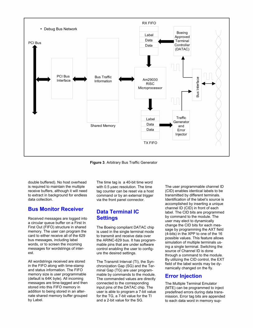
Bus Traffic Generator This feature is very similar to the MTE mode except it enables free-form, non-scheduled emulation of up to 120 terminals. The user sets up transmit information whose struc-ture is unconstrained by the ARINC-629 timing scheme and other limita-tions. This enables creating traffic of a more arbitrary nature to stress devices on the bus. See Figure 3 for a block diagram.
PCI-629 Architecture The PCI-629 contains the following hardware functional blocks: • PCI bus Interface
• 4M byte shared memory • On-board CPU • Transmit (TX) FIFO memory • Receive (RX) FIFO memory • Traffic Generator logic • Terminal Controller (DATAC) de-
vice • Serial 629 bus Interface Module
(SIM). When the PCI-629 is in the MTE mode of operation, the transmitter of the on-board DATAC is switched out of operation and a highly pro-grammable, specially developed Traffic Generator is switched into its place. The shared memory, which can be accessed by the host PC via the PCI interface and by the PCI-629 internal CPU, provides a global data storage resource. Information required for this mode of operation is stored in the shared memory by the user. The CPU takes the information stored by the user and converts it into the format required for the Traf-fic Generator. The Traffic Generator communicates with the onboard CPU via the TX FIFO memory which was used in order to utilize the maximum throughput of the CPU. Loading of the data by the CPU into the TX FIFO memory is asynchronous to the activity of the 629 interface (DATAC and/or Traffic Generator), freeing the CPU to serve other functions as well, such as PC host communication. The Traffic Generator reads infor-mation written to the TX FIFO by the CPU and uses the timing, control, and data content and converts it to waveforms required for bus opera-tion. The Traffic Generator, besides its normal transmit function, allows the injection of a wide variety of errors into the normal bus traffic.
Shared Memory All ARINC-629 data is sent from and received into an on-board three-port shared memory. Up to 4 Mbyte of memory is allocated to the transmit data and the multiple received data buffers. The memory is accessible to the onboard 29030, the DATAC chip transmitter logic, and to the host computer. Arbitration of the shared memory is transparent to all parties. The user can program multi-ple wordstring buffers (default is
double buffered). No host overhead is required to maintain the multiple receive buffers, although it will need to extract in background for endless data collection. Bus Monitor Receiver Received messages are logged into a circular queue buffer on a First In First Out (FIFO) structure in shared memory. The user can program the card to either receive all of the 629 bus messages, including label words, or to screen the incoming messages for wordstrings of inter-est. All wordstrings received are stored in the FIFO along with time-stamp and status information. The FIFO memory size is user programmable (default is 64K byte). All incoming messages are time-tagged and then stored into this FIFO memory in addition to being stored in an alter-nate shared memory buffer grouped by Label.
The time tag is a 40-bit time word with 0.5 μsec resolution. The time tag counter can be reset via a host command or by an external trigger via the front panel connector. Data Terminal IC Settings The Boeing compliant DATAC chip is used in the single terminal mode to transmit and receive data over the ARINC-629 bus. It has program-mable pins that are under software control enabling the user to config-ure the desired settings. The Transmit Interval (TI), the Syn-chronization Gap (SG) and the Ter-minal Gap (TG) are user program-mable by commands to the module. The commanded values are directly connected to the corresponding input pins of the DATAC chip. The user is able to program a 7-bit value for the TG, a 7-bit value for the TI and a 2-bit value for the SG.
The user programmable channel ID (CID) enables identical labels to be transmitted by different terminals. Identification of the label’s source is accomplished by inserting a unique channel ID (CID) in front of each label. The CID bits are programmed by command to the module. The user may elect to dynamically change the CID bits for each mes-sage by programming the AXT field (4-bits) in the XPP to one of the 16 possible values. This feature allows simulation of multiple terminals us-ing a single terminal. Switching the source of Channel ID is done through a command to the module. By utilizing the CID control, the EXT field of the label words may be dy-namically changed on the fly. Error Injection The Multiple Terminal Emulator (MTE) can be programmed to inject predefined errors during data trans-mission. Error tag bits are appended to each data word in memory sup-
Figure 3. Arbitrary Bus Traffic Generator
Shared Memory
PCI Bus
Bus Traffic Information Am29030
RISCMicroprocessor
TX FIFO
LabelDataData
TrafficGenerator
and Error
Injector
RX FIFO
LabelDataData
BoeingApprovedTerminal Controller(DATAC)
PCI BusInterface
▪ Debug Bus Network

porting errors on a word-by-word basis. Word/Bit level errors are gen-erated by dedicated hardware and are injected each word depending on the tag bits. There are a few er-rors that the user can program at the protocol level such as a Short String Error, an Impersonation Er-ror, etc. The following errors can be generated: Parity Error Inverted (Even) parity bit is sent to the 629 bus on a word-by-word ba-sis. Inverted Sync Error The 3 Sync bits of any word can be inverted on a word-by-word basis. Sync Bit Error The 3 Sync bits can be distorted with a Manchester Bi-Phase type error on a word-by-word basis. Manchester Error Illegal Manchester Bi-Phase bits are inserted anywhere in the 20-bit Manchester word format (including Sync and Parity bits). The Manches-ter error can be programmed in 1/4 bit resolution to any combination of high, low and mid (gap) levels for each of the four 1/4 bit slices. Can be programmed on a word-by-word basis. Short Word Error A bit is replaced with a single-bit gap at the tail end of the word on a word-by-word basis. Long Word Error An additional bit is appended to the last bit of the last word of a word-string. Bus Contention Error An ARINC-629 bus contention is generated by enabling the SIM to send a word whenever another ter-minal is transmitting. This is com-prised of one Manchester bit, creat-ing a one bit data contention. Impersonation Error The XPP can be programmed to send the same CID bits as another transmitter, causing an impersona-tion error. This does not require any hardware intervention being sup-ported by the downloadable person-ality PROM of the PCI-629 card. Short String Error The XPP can be programmed to
send fewer words in the wordstring than is expected by the UUT. This error does not require any hardware intervention being supported by the downloadable personality PROM of the PCI-629 card. End-of-String Error The XPP can programmed to send more words than is expected by the UUT for the particular wordstring. This error does not require any hardware intervention being sup-ported by the downloadable XPP of the PCI-629 card. Frequency Error The clock source for the PCI-629 can be selected from one of four possible data rates: 32 MHz (nominal), 30 MHz (low), 33 MHz (high) or External Clock input from the front panel connector. This sup-ports stressing the receive timing of terminals on the bus.
Receiver Errors Detection The ARINC-629 receiver circuitry is capable of detecting both protocol and format (hardware) type errors. This is performed by the DATAC chip and by post-processing of the received messages by the on-board microprocessor. The following er-rors can be detected: Parity Error Inverted (Even) parity bit is received from the 629 bus. Impersonation Error The received label’s extension does not agree with the terminal’s CID when the MSC field in the appropri-ate RPP cell is not equal to 1F hex. Short String Error The received wordstring was shorter than expected and it terminated prematurely. RERF Error This indicates that the DATAC chip encountered a data integrity error, possibly an improper Manchester code, SYNC or parity bit error. PAM0 Error This indicates a disagreement be-tween the RPP content and the TG or SG register. PAM1 Error
This indicates a disagreement be-tween the RPP content and the TI register. Bus-Monitor Error Detection The DATAC chip contains a built-in bus monitor that can detect errors associated with the reception of data that is being transmitted by the terminal itself. The following errors can be detected: End of String Error The received wordstring contains more words than are expected by the UUT. End of Message Error The number of actual wordstrings exceeds the Message String Count (MSC) field of the RPP. Data Error A Manchester encoding error, parity or Sync error. Label Error A label word Manchester encoding error, parity or Sync error. XERF Error This indicates detection of a data integrity error, which prevented transmission. This error is flagged by the DATAC internal Error regis-ter. TXE Indicates that the transmitter was permanently shut off due to detec-tion of multiple (7) errors. To re-enable the transmitter of the DATAC, the chip must be reset. Note applies only in a single termi-nal mode where the DATAC trans-mitter is enabled. Bus Quiet Error One or more transmit word is miss-ing, thereby creating an unexpected bus quiet state. ARINC-629 Bus Rate The ARINC-629 bus clock source is programmable: on-board 32 MHz XTAL oscillator (nominal), on-board 30 MHz XTAL oscillator (slow), on-board 33 MHz XTAL oscillator (fast), external clock source via the front panel connector. The selected clock source can optionally be divided by two to provide ARINC-629 protocol compatible operation, but running at

MIL-STD-1553 data rates (1M baud nominal).
PCI Bus Interface The PCI-629 is a single-slot, single function 5V/32-bit 33MHz PCI de-vice fully compliant to Revision 2.1 of the PCI Bus Specification. The PCI-629 uses the PCI bus INTA# line for all interrupts to the host.
Parallel I/O The PCI-629 contains eight 5V TTL compatible general purpose parallel I/O signals. The 8-bit parallel I/O port outputs can be enabled or tri-stated by sending a command to the card.
LEDs Four LED indicators are located on the card: RST red LED indicates that the on-board CPU is being reset by the host. FAIL red LED is lit upon power-up when the CPU executes its self test. If lit for more than 5 seconds, it indi-cates a self-test failure. PCI green LED indicates that the device is being accessed by the host through the PCI bus. 629 green LED is lit every time that the device is transmitting data over the ARINC-629 bus.
Reset Switch A push-button momentary switch on the card can be used to reset the card in a similar mode to a power-up reset.
SIM/CMC Power +/- 15V power for the SIM and CMC are provided by an on-board DC-DC converter. The user can also config-ure the card to receive input power for the SIM and CMC from the front panel connector.
Connection to Multiple Busses A number of Units Under Test (UUTs) contain more than one ARINC 629 interface. The PCI-629 can simplify the testing of these UUTs by being wired to up to 4
separate ARINC 629 buses at any one time. The 4 sets of transmit/receive (both Pseudo Bus and SIM Bus) signal pairs are available at the front panel connector of the card. The SIM Bus ports require an exter-nal CMC each. The transmit and receive signal pairs for the SIM Bus are switched into the on-board SIM channel using electromechanical relays. Switching is performed entirely under host software control, eliminating the need for any manual intervention during testing. For the Pseudo Bus, the on-board circuitry is used to switch the trans-mitter and receiver to the individual signal pairs logically. High-current, open-collector drivers are used for each of the Pseudo Bus signal pairs. Two 60 ohm termination re-sistors are also provided at the front panel connector for each Pseudo Bus signal pair. Note that these signals may be toggling when the SIM Bus is selected as active.
Front Panel Connector The front panel of the PCI-629 con-tains an ARINC-629 interface con-nector. This connector enables ac-cessing up to four ARINC-629 SIM Bus CMC couplers, up to four Pseudo Bus interfaces, external triggers, external bus synchroniza-tion signals, the external clock input, external +/- 15V SIM/CMC power inputs, and the 8-bit parallel I/O lines. This is a 68-pin female SCSI-II type connector that consists of two rows of 34 pins, spaced 0.1" apart with 0.050" contact spacing in each row. The construction of this connector offers exceptional EMI/RFI shielding effectiveness when used with shielded cable plugs. See Figure 2 for a depiction showing pin assign-ments. Table 2 identifies the signals (GND and reserved signals not shown). A wide variety of both shielded and unshielded connectors which mate with this connector are available. Single-ended cable assemblies which mate with it are also avail-able. Contact Corelis for details.
Host Software Application software is provided to assist the user to quickly set up and observe card behavior. The PCI-629 Device Utility is a graphical user interface (GUI) that provides an easy way to transmit, receive, moni-tor and in general exercise the func-tionality of PCI-629 card. For us-ers who prefer the most flexibility, custom “C" application software can be written using the PCI-629 Instru-ment Driver. Note: Familiarity with the ARINC-629 specification and with the 629 Avionics bus DATAC, SIM and CMC components is required in order to use this card and in order to write host application software that util-izes this card. The PCI-629 Device Utility, compati-ble with Windows™2000/XP, pro-vides card behavior visibility. It in-cludes text script files which define the downloaded configuration and transmit data. A GUI screen shows periodically updated real-time infor-mation being transmitted and re-ceived over the 629 bus. The main set-up screen is shown in Figure 4. This application can operate up to two PCI-629 cards in the same host PC. Using Pseudo Bus (which can receive its own transmission on the bus with no external wiring), a single card can generate and report 629 bus traffic. Loopback for the SIM Bus requires an external CMC and ARINC-629 bus installation, since the CMC can report its own traffic coupled to the bus. If two such cards are running, both can observe each other’s traffic. This requires a pin-to-pin loopback cable for Pseudo Bus or a live exter-nal ARINC-629 link between cards using CMCs for the SIM Bus selec-tion. PCI-629 Instrument Driver software provides the capability to access all PCI-629 functionality. Users who desire to write their own software will find this low level “C” driver soft-ware very useful. These functions make it easier to write custom appli-cation software and drastically re-duce the software development effort.

An example application is provided to help you get started using the PCI-629 Instrument Driver. The example application generates loop-back traffic and reports received data to a console screen. It em-ploys calls to the provided “C” driver functions transparently handling the low level details of card control and simplifying application development. The example application includes source code which can be modified and re-built.
Figure 4. PCI Device Utility Main Screen

PCI-629 Hardware Specifications:
PCI Bus Interface
Device Type Target with shared memory interface. PCI interrupter. Memory mapped.
Address/Data Bus Width 32-bit
I/O Type 5V Clock Frequency 0 - 33MHz
Interrupt Lines Used INTA#
Power Requirements 5V (5A maximum) 12V (100 mA maximum)
Shared Data Memory
Total Memory 4M Byte
Dual-Port Host and local CPU accessible with transparent arbitration.
Data Width 8, 16 or 32-bit
On-board CPU
Processor Type AMD Am29030 RISC, 32-bits
Personality PROMs
XPP Memory Four XPP memories, 8K Byte each, 32K Byte total. Host downloadable.
RPP Memory Host downloadable 32K Byte RPP memory.
MPP Memory Host downloadable 64K Byte MPP memory.
ARINC-629 Interface Data Terminal IC National Semiconductor AR629AU9-MC1 (or equivalent) IC
SIM AMP 448044-1 (or equivalent) IC
Modes of Operation Periodic (A-Mode), Aperiodic (BMode), C-Mode Scheduling Block, Independent, Alternate, Synchronized
Clock Data Rate 2MHz (nominal)
Other Clock Rates +3%, -6%, External
Receive Queue
Continuous Buffer Circular buffer type, 512K byte, shared memory based Label Queue Buffer Labels buffer records bus events. Size is 256K byte One-Shot Buffer Armed by trigger, then receives until full. Size is 256 Kbyte Data Format Complete wordstrings stored, each includes time-stamp and
status words Time Stamp Words 40-Bit time-stamp, 0.5 μs resolution Status Word 16-Bits status with error bits
ARINC-629 Bus Monitor
Data Format Each wordstring is received in full: Label Word, Data Word(s), Time Stamp, Status.
Label Filter Receives all or filtered bus messages
Table 3. PCI-629 Hardware Specifications
▪ Debug Bus Network

PCI-629 Hardware Specifications (continued):
Table 3. PCI-629 Hardware Specifications (continued)
Error Insertion
Method Error code tag for each transmit word.
Number of Errors One per word, unlimited number of words, any time, any word(s), any message(s)
Error Types Parity error Manchester error (1/4 bit resolution), Inverted sync error, Sync Manchester error, Long word error, Short word error, Bus quiet error, Pre-sync pulse error, Pre-pre-sync pulse error, Inter-wordstring short gap error, Inter-wordstring long gap error
Error Injection Order User specified arbitrary order
Frequency Error Clock source programmable: 32MHz (nominal), 33MHz, 30MHz, External (user supplied)
Multiple Terminal Emulator Programmable to 120 terminals Both Periodic and Aperiodic User Specifies up to 120 XPPs in shared memory Transmit Order User specified terminal order Word-by-Word basis, any word Error Detection Status bits for each Wordstring
ARINC-629 Bus Coupling
Coupling Type Current Coupler SIM with user provided (external) CMC interface, up to 4 CMCs can be connected at one time, relay switch-able under software control
Voltage Coupler Open Collector Pseudo Bus Interface, 190 mA current sink , 4 bus connections available, logic switch-able under software control
Pseudo Bus Termination Eight 59 ohm pull-up resistors, 2 for each of the 4 pseudo bus signal pairs are available at the front connector
Jumper Settings
SIM +/-15 V Power Selects from on-board DC-DC Converter or external power from front panel connector. Other jumpers locations are reserved for factory testing.
Triggers
Front Panel One Trigger_In, One Trigger_Out TTL signals Trigger Output Timing User selectable, any wordstring, leading or trailing the wordstring
Physical Characteristics
Size Single slot, long card
Dimensions Approx. 12.283"L x 4.200"H
Connector AMP 750737-7 (or equivalent), 68- pin SCSI-II type, female
LEDs Four: Rst (red), Fail (red) , PCI (green), 629 (green)
Deliverable PCI-629 Board CDROM (Including installable software and user manual files)
Ordering Information Part Number 10095A (PCI-629)
▪ Debug Bus Network

CORELIS
12607 Hidden Creek Way Cerritos, California 90703 Telephone: (562) 926-6727, Fax: (562) 404-6196 [email protected] www.corelis.com
Windows is a trademark of Microsoft Corporation. PCI-629 is a trademark of Corelis Inc. All other trademarks referred to herein are the property of their respective owner. © Copyright 2007 by Corelis Inc. All rights reserved. CORELIS Inc., reserves the right to make changes in design or specification at any time without notice. Revision: 07.12.2007