penn statev - dtic · block 3. type of report and dates covered. state whether report is interim,...
TRANSCRIPT

NANOCOMPOSITES FOR ELECTRONIC APPLICATIOI
Period January 1, 1990 thru December 31, 1991
FINAL REPORT
Volume IIIIN
I• OFFICE OF NAVAL RESEARCH
Contract No. N00014-90-J-1558
APPROVED FOR PUBUC R E - DISTRIBUTION UNLIMITED
Reproduction in whole or in part is permitted for any purposeof the United States Government
L. Eric Cross DT•
JUL22 199$
PENN STATEVTHE MATERIALS RESEARCH LABORATORY
UNIVERSITY PARK, PA
S,• 7 2 1.•.4$g 93-16532•";! iI 3,2I'• F
11P •r, I

DIS CLAIMJI NOTWK
THIS DOCUMENT IS BEST
QUALITY AVAILABLE. THE COPY
FURNISHED TO DTIC CONTAINED
A SIGNIFICANT NUMBER OF
PAGES WHICH DO NOT
REPRODUCE LEGIBLY.
L •

REPORT DOCUMENIAIIUN PA(i OMB No. 0704-0188
"Piac rifis oni g burden for this collection of ilormallOn as etlimated to average I hour oit rt'* onste including the time ot rev~ew.nj tinstiuctiotns. tearchiq itst#,nj dalti sources
gathetring an maintaining the data needed. and cowrtetein and rewierig the. co.te•1ion of riMmition lend comments re.•arding this buiden estimate cr %no flhues s.ect of metCoUectmOi of Information. including suggestion%, ctO reduing this bstat.n to *Wahinglon ieardauartes Service%. DirectOrate for intoumateorn i oitittons 4ald •B•tv. II1I leJefferon
DaIvi jughWSy. $Suli 1t04. Arlington. Va 2202-4 102 4ud to the '.|fict ef MA4nagement and Budget. P•DwOrk Aeduibon Prop.t (I010O 0 18) wash-fPqt10 DC M03OI
1. AGENCY USE ONLY (Leave blank) 2. REPORT DATE 3. REPORT TYPE AND DATES COVERED
1 06/14/93 I FINAL REPORT 01/01/90 To 12/31/914. TITLE AND SUBTITLE S. FUNDING NUMBERS
NANOCOWOSITES FOR ELECTRONIC APPLICATIONS
6. AUTIHOR(S)
L. ERIC CROSS
7. PERFORMING ORGANIZATION NAME(S) AND AODRESS(ES) B. PERFORMING ORGANIZATION
MATERIALS RESEARCH LABORATORY REPORT NUMBER
THE PENNSYLVANIA STATE UNIVERSITYUNIVERSITY PARK, PA 16802 NOOO14-90-J-1558
9. SPONSORING/ MONITORING AGENCY NAME(S) AND AOORESS(ES) 10. SPONSORING/MONITORING
OFFICE OF NAVAL RESEARCH DOUGLAS E. HEATON AGENCY REPORT NUMBER
CODE 1513:MBL DEPT. NAVY/ONR, RES. REP.800 NORTH QUINCY STREET THE OHIO STATE UNIV. RES. CTR.ARLINGTON, VA 22217 1960 KENNY ROAD
COLUNBUS, OH 43210-10611t. SUPPLEMENTARY NOTES
12a. DISTRIBUTION I AVAILABILITY STATEMENT 12b. DISTRIBUTION CODE
S13. ABSTRACT (Maximum 200 words)
SEE FOLLOMING PAGES.
14. SUBJECT TERMS 15. NUMBER OF PAGES
16. PRICE CODE
"17. SECURITY CLASSIFICATION lB. SECURITY CLASSIFULAIION 19. SECURITY CLASSIFICATION I20. LIMITATION OF ABSTRACT
(-F REPORT OF THIS PAGE OF ABSTRACT
NSN 7S40-01280-andad Form 298 (; v 11 ),sfibtd byA| iS. 1'

GENERAL INSTRUCTIONS FOR COMPLETING SF 298The Report Documentation Page (RDP) is used in announcing and cataloging reports. It is importantthat this information be consistent with the rest of the report, particularly the cover and title page.Instructions for filling in each block of the form follow. It is important to stay within the lines to meetoptical scanning requirements.
Block 1. Agency Use Only (Leave blank). Block 12a. Distribution/Availability Statement.Denotes public availability or limitations. Cite any
Block 2. Report Date. Full publication date availability to the public. Enter additionalincluding day, month, and year, if available (e.g. 1 limitations or special markings in all capitals (e.g.Jan 88). Must cite at least the year. NOFORN, REL, ITAR).
Block 3. Type of Report and Dates Covered.State whether report is interim, final, etc. If DOD - See DoDD 5230.24, Distributionapplicable, enter inclusive report dates (e.g. 10 Statements on TechnicalDocuments. *
Jun 87 - 30 Jun 88). DOE See authorities.
Block 4. Title and Subtitle. A title is taken from NASA - See Handbook NHB 2200.2.the part of the report that provides the most NTIS - Leave blank.meaningful and complete information. When areport is prepared in more than one volume, Block 12b. Distribution Code.repeat the primary title, add volume number, andinclude subtitle for the specific volume. Onclassified documents enter the title classification DOD - Leave blank.in parentheses. DOE Enter DOE distribution categories
from the Standard Distribution forBlock 5. Funding Numbers. To include contract Unclassified Scientific and Technicaland grant numbers; may include program Reports.element number(s), project number(s), task NASA - Leave blank.number(s), and work unit number(s). Use the NTIS Leave blank.
following labels:
C - Contract PR - Project Block 13. Abstract. Include a brief (MaximumG - Grant TA - Task 200 words) factual summary of the mostPE - Program WU - Work Unit significant information contained in the report.
Element Accession No.
Block 6. Author(s). Name(s) of person(s) Block 14. Subiect Terms. Keywords or phrasesresponsible for writing the report, performing identifying major subjects in the report.the research, or credited with the content of thereport. If editor or compiler, this should followthe name(s). Block 15. Number of Pages. Enter the total
number of pages.Block 7. Performing Organization Name(s) andAddress(es). Self-explanatory. Block 16. Price Code. Enter appropriate price
Block 8. Performing Organization Report code (NTIS only).Number. Enter the unique alphanumeric reportnumber(s) assigned by the organization Blocks 17.- 19. Security Classifications. Self-performing the report. explanatory. Enter U.S. Security Classification in
Block 9. Sponsoring/Monitoring Agency Name(s) accordance with U.S. Security Regulations (i.e.,and Address(es). Self-explanatory. UNCLASSIFIED). If form contains classified
information, stamp classification on the top andBlock 10. Sponsoring/Monitoring Agency bottom of the page.Report Number. (If known)
Block 11, Supplementary Notes. Enter Block 20. Limitation of Abstract. This block mustinformation not included elsewhere such as: be completed to assign a limitation to thePrepared in cooperation with...; Trans. of...; To be abstract. Enter either UL (unlimited) or SAR (samepublished in.... When a report is revised, include as report). An entry in this block is necessary ifa statement whether the new report supefedes the abstract is to be limited. If blank, the abstract
or supplements the older report. is assumed to be unlimited.
Standard Form 298 Back (Rev. 2-89)

ABSTRACT
This document is the final report of work on the DARPA sponsored University Research
Initiative (URI) on the subject "Nanocomposites for Electronic Applications" funded under ONR
Contract No. N00014-90-J-1558. Initial funding on the contract was for a three year period from
1987-1990. This document is the final report for the two year extension period finishing on
December 31, 1991.
Work on this program and associated studies on the ONR program on "Piezoelectric and
Electrostrictive Materials for Transducer Applications" has lead to a significantly improved
understanding of the fundamental mechanisms in Relaxor Ferroelectrics. For the perovskite Lead
Magnesium Niobate which is the prototype for many other relaxor perovskites, the self limiting
nonstoichiometric ordering of Mg/Nb ions is shown to be the symmetry breaking key to the onset
of micropolar regions at the Burns temperature well above the dielectric maximum. The simple
paraelectric behavior at high temperature is shown to be modified by cooperation on cooling,
leading to a Vogel:Fulcher type condensation into a glass like state at low temperature.
Many tungsten bronze structure ferroelectrics e.g. Srl-xBaxNb2O6 also show relaxor
ferroelectric behavior, and in the lead barium niobate family of solid solutions there is a particularly
rich panoply of behaviors. Depending on composition polarization may appear along the 4 fold
axis, or along one of the orthogonal 2 fold axes of the prototypic 4/mmm prototype. In PBN a
pseudo morphotropic phase boundary (PMPB) exists near the 60:40 Pb:Ba composition. The
intriguing feature for the PBN compositions is that for the tetragonal symmetry, the permittivity
increases for directions orthogonal to the 4 fold axis and there is a second freezing (in the polar
state) near 1OOK. At the MPB the symmetry may be switched by electric field to that with macro-
polarization along 2 (orthorhombic) and now the second freezing takes place for polarization along
4. The low temperature freezing occurs whether the initial phase is glassy or ferroelectric and
gives rise to fascinating families of unusual dielectric, piezoelectric, elastic and optical properties.
A second important contribution on this program stemmed from the very careful preparative
studies to make ultra find powders of simple perovskite ferroelectrics. The objective was to obtain
understanding of the intrinsic size effects which must occur in ferroelectrics due to the cooperative
nature of the phenomenon. From studies of spontaneous strain it was made clear that
ferroelectricity in BaTiO3 did not occur in powders with particular size less than 800"A whereas in
PbTiO3 ferroelectricity and spontaneous strain persists down to sizes of order 170OA.
In 0:3 type composites it is natural to have a major interest in the phenomenon of
peicolation, and of the critical concentrations for this phenomenon. Practical aspects of this work
occur in the PTC polymer:carbon composites and in other systems.

Fundamental studies on silicon, germanium and silica germania composites usingwavelength scanning ellipsometry have lead to the evolution of effective techniques for theevaluation of inhomogeneity in highly transparent oxides, in systems with uniaxial anisotropy andhave validated spectroscopic cJlipisometry as one of the most valuable nondestructive techniquesfor the study of ferroelectric surfaces and thin films.
lOT
I" o -- 2 -t t!ij_
1 X~ $,d

NANOCOMPOSITES FOR ELECTRONIC APPLICATIONS
Period January 1, 1990 thru December 31, 1991
FINAL REPORT
Volume III
OFFICE OF NAVAL RESEARCH
Contract No. N00014-90-J-1558
APPROVED FOR PUBLIC RELEASE - DISTRIBUTION UNLIMITED
Reproduction in whole or in part is permitted for any purposeof the United States Government
L. Eric Cross
PENNSTATEVTHE MATERIALS RESEARCH LABORATORY
UNIVERSITY PARK, PA

TABLE OF CONTENTS
ABSTRACT .................................................... 5
1.0 INTRODUCTION ........................................... 7
2.0 GENERAL PAPERS .......................................... 8
3.0 RELAXOR FERROELECTRICS ................................. 8
4.0 MICRO COMPOSITES STUDIES ................................ 9
5.0 INTRINSIC SIZE EFFECTS IN FERROELECTRICS ................... 10
6.0 SPECTROSCOPIC ELLISOMETRY ............................... 10
7.0 INVITED LECTURES ........................................ 11
8.0 CONTRIBUTED PAPERS ..................................... 12
9.0 HONORS TO MRL FACULTY AND STUDENTS ..................... 14
APPENDICES
General Summary1. L. Eric Cross. "Ferroelectric Ceramics: Tailoring Properties for Specific Applications,"
Proceedings of the Summer School on Ferroelectrics, Ascona, Switzerland(September 1991).
Relaxor Ferroelectrics2. R. E. Newnham and T. R. Shrout. "Electronic Ceramics," Advanced Ceramics
(Electronic), Vol. 1, pp. 601.
3. D. D. Viehland. "The Glassy Behavior of Relaxor Ferroelectrics," PhD Thesis, Solid StateScience, The Pennsylvania State University (May 1991).
4. R. Guo. "Ferroelectric Properties of Lead Barium Niobate Compositions Near theMorphotropic Phase Boundary," PhD Thesis, Solid State Science, The Pennsylvania StateUniversity (December 1990).
5. D. A. McHenry. "Optical and Electrooptical Properties of Lead Magnesium Niobate-LeadTitanate," PhD Thesis, Solid State Science, The Pennsylvania State University(May 1992).
6. Jayne R. Giniewicz. "An Investigation of the Lead Scandium Tantalate-Lead Titanate SolidSolution System," PhD Thesis, Solid State Science, The Pennsylvania State University(December 1991).

APPENDICES (continued)
7. A. S. Bhalla, R. Guo, L. E. Cross, G. Bums, F. i-H. Dacol, and R. R. Neurgaonkar."Glassy Polarization in the Ferroelectric Tungsten Bronze (BaSr)Nb20 6," J. Appl. Phys.71 (11), 5591 (1992).
8. C. A. Randall, R. Guo, A. S. Bhalla, and L. E. Cross. "Microstructure-PropertyRelations in Tungsten Bronze Lead Barium Niobate Pbj-xBaxNb 2O6 ," J. Mat. Res. t (8),1720 (1991).
9. R. Guo, A. S. Bhalla, and L. E. Cross. "Pyroelectric Properties of Lead Barium NiobateSingle Crystals," Ferroelectrics 118, 77 (1991).
10. D. Viehland, S. J. Jang, L. E. Cross, and M. Wuttig. "The Dielectric Relaxation of LeadMagnesium Niobate Relaxor Ferroelectrics," Phil Mag B 64 (3), 335 (1991).
11. D. Viehland, S. J. Jang, L. E. Cross, and M. Wuttig. "Anelastic Relaxation and InternalStrain in Lead Magnesium Niobate Relaxors," Phil Mag A 64 (4), 835 (1991).
12. D. Viehland, S. J. Jang, L. E. Cross, and M. Wuttig. "Local Polar Configurations in LeadMagnesium Niobate Relaxors," J. Appl. Phys. 69 (1), 414 (1991).
13. D. Viehland, M. Wuttig, and L. E. Cross. "The Glassy Behavior of the RelaxorFerroelectrics," Ferroelectrics 120, 71 (1991).
14. D. Viehland, S. J. Jang, L. E. Cross, and M. Wuttig. "Freezing of the PolarizationFluctuations in Lead Magnesium Niobate Relaxors," J. Appl. Phys. 68 (6), 2916 (1990).
15. J. R. Giniewicz, A. S. Bhalla, and L. E. Cross. "Lead Scandium Tantalate - Lead TitanateMaterials for Field Stabilized Pyroelectric Device Applications," Ferroelectrics Letters 14,21(1992).
16. J. R. Giniewicz, D. A. McHenry, T. R. Shrout, S. J. Jang, A. S. Bhalla, and F. Ainger."Characterization of (1-x) PbMgl/3Nb2/30 3-xPbTiO3 and PbScl/2Ta1/203 TransparentCeramics Prepared by Uniaxial Hot Pressing," Ferroelectrics 109, 167 (1990).
17. J. R. Giniewicz, A. S. Bhalla, and L. E. Cross. "Pyroelectric Response andDepolarization Behavior of (I-x) PbSc j/2Tal/2O3-xPbTiO3 Materials," Ferroelectrics 118,157 (1991).
18. D. A. McHenry, J. R. Giniewicz, T. R. Shrout, S. J. Jang, and A. S. Bhalla. "Electricaland Optical Properties of Relaxor Ferroelectrics," Ferroelectrics 102, 161 (1990).
19. D. A. McHenry, J. R. Giniewicz, S. J. Jang, T. R. Shrout, and A. S. Bhalla. "Opticaland Electro-optical Properties of Lead Magnesium Niobate:Lead Titanate," Ferroelectrics107, 45, (1990).
2

APPENDICES (continued)
20. D. A. McHenry, J. Giniewicz, S. J. Jang, A. S. Bhalla, and T. R. Shrout. "OpticalProperties of Hot Pressed Relaxor Ferroelectrics," Ferroelectrics 23, 351 (1989).
21. G. R. Fox, J. K. Yamamoto, D. V. Miller, L. E. Cross, and S. K. Kurtz. "ThermalHysteresis of Optical Second Harmonic in Paraelectric BaTiO3," Materials Letters 2 (7, 8),284 (1990).
Micro Composites Studies22. G. R. Harshe. "Magnetoelectric Effect in Piezoelectric-Magnetostrictive Composites,"
PhD Thesis, Solid State Science, The Pennsylvania State University (August 1991).
23. G. Harshe, J.Dougherty, and R. E. Newnham. "Magnetoelectric Effect in CompositeMaterials," Proceedings Conference on Smart Materials and Structures, SPIE,Albuquerque, NM (February 1-4, 1993).
24. G. Harshe, J. P. Dougherty, and R. E. Newnham. "Theoretical Modelling of 3-0/0-3Magnetoelectric Composites," Submitted, Int. J. of Appl. Electromagnetics in Materials.
25. G. Harshe, J. P. Dougherty, and R. E. Newnham. "Theoretical Modelling of MultilayerMagnetoelectric Composites," Submitted, Int. J. of Appl. Electromagnetics in Materials.
26. R. J. Sullivan and R. E. Newnham. "Composite Thermistors," Chemistry of AdvancedMaterials, Edited by C. N. R. Rao, Blackwell Scientific Pubhications (1992).
27. G. R. Ruschau, S. Yoshikawa, and R. E. Newnham. "Percolation Constraints in the Useof Conductor-Filled Polymers for Interconnects," Proc. Elect. and Comp. Tech., IEEE,San Diego (May 18-20, 1992).
28. M. Blaszkiewicz, D. S. McLachlan, and R. E. Newnham. "The Volume Fraction andTemperature Dependence of the Resistivity in Carbon Black and Graphite PolymerComposites: An Effective Media Percolation Approach."
29. G. R. Ruschau, S. Yoshikawa, and ,'R. E. Newnham. "Resistivities of ConductiveComposites," J. Appl. Phys. 22 (3), 953 (1992).
30. D. M. Moffatt, J. Runt, W. Huebner, S. Yoshikawa, and R. E. Newnham. "PTC Effectsin Conductor Filled Amorphous Polymer Composites," PTC Effects in PolymerComposites, Chapter 3, pp. 51.
Intrinsic Size Effects in Ferroelectrics31. R. E. Newnham, K. R. Udayakumar, and S. Trolier-McKinstry. "Size Effects in
Ferroelectric Thin Films," Book Chapter, Chemical Processing of Advanced Materials,Editor L. Hench, J. K. West, John Wiley & Sons Inc. (1992).
Spectroscopic Ellipsometry32. N. Van Nguyen. "Spectroscopic Ellipsometry of Interfaces," PhD Thesis, Physics, The
Pennsylvania State University (November 1989).
3

APPENDICES (continued)
33. P. Chindaudom. "Characterization of Inhomogeneous Transparent Thin Films onTransparent Substrates by Spectroscopic Ellipsometry," PhD Thesis, Physics, ThePennsylvania State University (August 1991).
34. N. V. Nguyen, K. Vedam, and J. Narayan. "Characterization of the Interface BetweenGe+ -Implanted Crystalline Silicon and Its Thermally Grown Oxide by SpectroscopicEllipsometry," J. Appl. Phys. 67 (2) (1990).
35. S. Trolier-McKinstry, H. Hu, S. B. Krupanidhi, P. Chindaudom, K. Vedam, and R. E.Newnham. "Spectroscopic Ellipsometry Studies on Ion Beam Sputter DepositedPb(ZrTi)0 3 Films on Sapphire and on PT Coated Silicon Substrates," Submitted, J. Appl.Phys.
36 J. Chen, K. R. Udayakumar, K G. Brooks, and L. E. Cross. "Dielectric Behavior ofFerroelectric Thin Films at High Frequencies," pp. 182, Proc. ISAF 92, Greenville, SouthCarolina.
37. K. R. Udayakumar, J. Chen, K. G. Brooks, L. E. Cross, A. M. Flynn and D. J. Ehrlich."Piezoelectric Thin Film Ultrasonic Micromotors," Mat. Res. Soc. Symp. Proc., Vol. 243,pp. 49-54 (1992 Materials Research Society).
4

MICRO-COMPOSITES STUDIES(continued)

APPENDIX 26

16 Composite Thermistors16~R.J. SULLIVAN and R.E. NEWNHAM
Materials Research Laboratory. The Pennsytvania State Unkersaty, University Park, PA 16802 LISA
1 Introduction
The combination of two or more phases to form a composite is a commonoccurrence in modem materials engineering. By combining phases, the functionalfigure of merit, which usually involves more than one property coefficient, can be
optimized. One such example of a functional composite is the conductive oxide-polymer positive temperature coefficient thermistor.
Thermistors, temperature-dependent resistors, are typically made from dopedceramic (BaTiO 3). The desire for improved properties and ease of processing hasspurred the development of composite thermistors. This type of composite com-bines a low resistivity filler powder, such as carbon black, vanadium sesquioxide, ornickel, with a high resistivity polymer matrix such as polyethylene or polystyrene.In the dormant room temperature state the thermistor has a resistivity similar tothe filler. On being activated by heating, however, the resistivity increases to a valueclose to the polymer matrix resistivity, often an increase of eight orders ofmagnitude.
2 Thermistors
Thermistors may be classified as one of two types. Negative temperature coefficient(NTC) thermistors exhibit a decrease in resistivity as temperature increases.Positive temperature coefficient (PTC) thermistors increase resistivity as tempera-ture increases. The temperature range over which the change in resistivity occurs,or rather the slope of the resistivity-temperature curve, is very important. Inapplications where the ambient temperature is to be determined by the resistivityof the thermistor, a gradual PTC transition would be required. If the thermistor isto be used as a current limiter, a very steep PTC transition is needed so that at a
given thermistor temperature the switch from the low to the high resistivity state israpid and the circuit protected. Critical temperature thermistors exhibit theirchange in resistivity over a very short temperature range. Resistivity curves forboth NTC and PTC thermistors are shown in Fig. 16.1.
In an electrical circuit the thermistor is placed in series with the load as shown in
Fig. 16.2. Configured in this way the thermistor must be invisible in the circuit,with low resistance in the dormant state. Once activated the thermistor resistancemust be large enough to protect the load. Some of the many applications forthermistors are as flow sensors, liquid level sensors, current limiters and thermalsensors [ 1,2]. Thermistors being used for these applications may be found in hairdryers, television degaussers and window motors in automobiles.
Regardless of how a thermistor is utilized in a product, it must meet some basic
requirements. The thermistor must not significantly change the total resistance of
351

352 R.J. SULLIVAN AND R.E. NEWNHAM
too
ti0
106
E 1os PTCE
S104"103
100
10-' t I I I i I
-200 0 200Temperature (C)
Fig. 16.1 Thermistor resistivity dependence upon temperature for a 30 vol%V20 3- polymethylmethacrylate composite. NTC, negative temperature coefficient; PTC,positive temperature coefficient of resistance. Measured at I kHz [26].1 °
j Rp~c
VA R'oW
I _ __ __V
VA_
RPTC + A~
Fig. 16.2 Circuit illustrating how a thermistor is used in series with a load. Current flowing inthe cirucit is calculated by the given equation.
the circuit in its dormant state (low room temperature resistance). Total change inresistivity of the thermistor and the temperature range over which it occurs must
suit the needs of the application. The power handling capabilities of the thermistormust allow normal circuit operation in the dormant state without switching to the
active state. And finally, as the temperature increases past the thermistor transition,
the electrical behavior of the thermistor must not be detrimental to the device. For
example, a decrease in resistivity after the transition in a PTC thermistor could notbe tolerated in many applications.
A PTC curve and the corresponding current-voltage (1-17) curve for a PTC
thermistor are shown in Fig. 16.3. Referring to Fig. 16.3, as the temperature of the
thermistor is increased to T, the resistivity remains constant, resulting in a linear
I-V characteristic up to point I. As the temperature increases through the PTC
transition (T"2) the resistivity increases dramatically and the I-V curve shows a
nonlinear decrease in current with increasing voltage (point 2). At higher tempera-

COMPOSITE THERMISTORS 3531011
_ E " characteristicS104
S 103'2S 10 ?20 Lz • \ \ oad line
100 1S
10o T1 T2 T3 33
10? l It 1 1 l i f0 50 100 150 200 VA
Temperature (C) Voltage
(a) (b)
Fig.16.3 (a) PTC resistivity curve for a 30 vol% V20 1 -polystyrene thermistor measured atI kHz [26). (b) Thermistor I-V characteristics derived from the PTC curve. Numbers denotepoints of importance for both curves.
tures (>T3) the resistivity once again becomes constant and a linear I-V relation-ship results (point 3). Points I and 3 are the two stable points of operation for athermistor.
When the PTC thermistor is in series with a load it may be switched from thehigh current phase to the low current phase in one of three ways [I]. If the voltageincreases, the load line shifts to higher voltages while maintaining the same slope,which results in the peak of the thermistor I-V curve dropping below the load line.Consequently, point 3 is the only stable point and the thermistor switches. Thethermistor is therefore used as protection against high voltage. An increase in thevoltage increases the power generated in the thermistor, which increases thethermistor temperature. At an elevated temperature the thermistor resistanceincreases and the voltage is limited. After the high voltage is removed the ther-mistor cools, the thermistor resistance returns to the lower value and the circuitonce again operates as designed.
In the event of the loss of load resistance the load line increases in slope. Oncethe thermistor I-V curve maxima falls below the load line the PTC thermistorswitches (again point 3 is the only stable point). Current stabilization and protec-tion against short-circuits are applications which take advantage of the PTCswitching in this fashion. A short-circuit or decrease in the load resistance increasesthe current in the circuit. The increased current heats the thermistor and switches itinto the high resistance state which limits the current in the circuit.
The third type of protection is against increases in the ambient temperature. Ifthe ambient temperature increases, the thermistor I-V curve changes (dotted line inFig. 16.3b). Again, point 3 is the only stable point and switching occurs. Thethermistor protects against overheating past the switching temperature by limitingcurrent flow. Applications capitalizing on the thermistor switching in this fashionare protection against overheated motors, temperature control and temperaturemeasurement [3]. For application as a temperature regulator in a hair dryer thethermistor is placed in the flow of warm air. As the air temperature heats past the

354 R.J. SULLIVAN AND R.E. NEWNHAM
switching temperature (T,) the thermistor switches to the active state and limits thecurrent to the load, in this case the heating coil. As the temperature falls below T,the thermistor resistance decreases and allows current to flow once again to theheating coil. Hence, the air temperature becomes stabilized at T7.
3 Ceramic thermistors
PTC thermistors manufactured from ceramics are typically BaTiO 3 based. Otherceramics such as chromium-doped vanadium sesquioxide ((VCr)20 3) also have aPTC behavior. Both systems have their own merits.
Barium titanate, when donor doped with elements such as La + 3(Ba, -_ La-TiO3)or NB * ' exhibits PTC behavior near its Curie temperature (Tc) [3-9]. At the Curietemperature the barium titanate switches from a ferroelectric tetragonal state to aparaelectric cubic state.
Grain boundaries are responsible for the PTC transition; hence, no PTC is seenin doped single crystal barium titanate [10, 11]. The ceramic thermistor must beprepared with a dopant or under a reducing atmosphere which results in semicon-ducting doped barium titanate. Reoxidation of the grain boundaries leaves theminsulating. Excess oxygen in the grain boundary creates an electron depletion regionnear the grain boundary. Consequently, electron conduction does not occur acrossthe grain boundary.
The spontaneous polarization of the barium titanate below Tc results in com-pensation of the charge at the grain boundary. The result is electron flow across thegrain boundary (low temperature dormant state). Once the temperature increasespast To, the barium titanate switches to the paraelectric cubic state, which destroysthe spontaneous polarization. Without the spontaneous polarization to compensatefor the charge at the grain boundary, electrons cannot flow across the grainboundary and the resistance of the doped barium titanate increases.
The change in resistivity may be up to six orders of magnitude (depending onprocessing). As the temperature increases even further above T, the bariumtitanate thermistor exhibits a gradual NTC. This is due to the increasing number ofelectrons which have enough thermal energy to jump over the barrier at the grainboundary. This NTC, as mentioned earlier, may render the PTC useless insome applications. Other drawbacks to doped barium titanate thermistors includedifficult processing and a relatively high room temperature resistivity (100 to1000 f-cm) 13,8).
Another ceramic which displays PTC as well as NTC thermistor behavior ischromium doped vanadium sesquioxide ((VCr)20 3) [12,13]. Both transitions, theNTC (- 1006C) and the PTC (between - 100 and 200"C) are discontinuousmetal-semiconductor transitions. The PTC transition is a bulk effect seen in bothsingle-crystal and polycr.stalline sauliples. and is only two orde'rs of iU:'lgnilude illsize. The low room temperature resistivity (10- ' fl-cm) and high current carryingcapabilities (200 A) make this composition a prime candidate for applications inwhich barium titanate thermistors are not suitable, but reproducible processing isdifficult.

COMPOSITE THERMISTORS 355
4 Composite thermistors
The need for thermistors with a lower room temperature resistivity and easierfabrication has led to the development of polymer composite thermistors. Carbon
black-polyethylene is the most widely used, commercially available composite
thermistor. Although dependent upon specific composition and processing, thecarbon black-polyethylene thermistors may exhibit a room temperature resistivitynear 1 12-cm and PTC magnitude of up to six orders [14,15]. Fillers such as V20 3,TiB2, and Ni in polythylene have also shown similar low room temperatureresistivities with even larger PTC steps (up to eight orders in magnitude). The PTCtransition occurs near the melting temperature of the semicrystailine polymermatrix.
Other systems being explored include conductive oxide as well as metal fillers inamorphous polymer matrices [16-24]. The electrical properties of these ther-mistors are comparable to those using a semi-crystalline matrix. With an amor-phous matrix, however, the PTC transition occurs near the glass transitiontemperature (T.) of the polymer matrix. In addition, the PTC transition in theamorphous polymer composites is typically not as steep as the semi-crystallinesystems.
The remainder of this chapter will describe the processing, electrical propertiesand mechanisms responsible for the PTC transition in the PTC composite ther-mistor. A significant effort has been put forth at the Pennsylvania State UniversityMaterials Research Laboratory to further understanding of composite thermistors.Electrical properties of the composite thermistor have been studied to determinehow processing, filler characteristics, polymer characteristics, and additional addi-tives affect its performance [ 15,16,18,25,26,34,74].
5 Processing
Basic processing of conductive filler-polymer composite thermistors is illustratedby the flowchart in Fig. 16.4. Detailed descriptions of each processing step arecontained in the literature [2,27-29].
The conductive filler and polymer are batched according to the polymer type.For a thermoplastic polymer (e.g. polyethylene or polystyrene) a high-temperature(I 60'C), high-shear mixer is used. For epoxies or other thermoset polymers,low-shear mixing is carried out at room temperature followed by curing at anelevated temperature (70'C).
In the case of a thermoplastic, the composite is further processed by usingpressure (20 000 psi) and elevated temperatures (1 50"C) to form the desiredthermistor shape. This shape may be a pellet or a sheet from which individualthermistors are punched. Attachment of metal foil electrodes, such as 50 prm Nifoil, is also accomplished in this step. In addition to making electrical contact withthe composite, the stiffness of the metal foil increases the high temperaturemechanical stability of the thermistor. The side of the foil in contact with thecomposite should be either mechanically or chemically roughened to promote
adhesion between the electrode and composite. As for the thermoset polymer
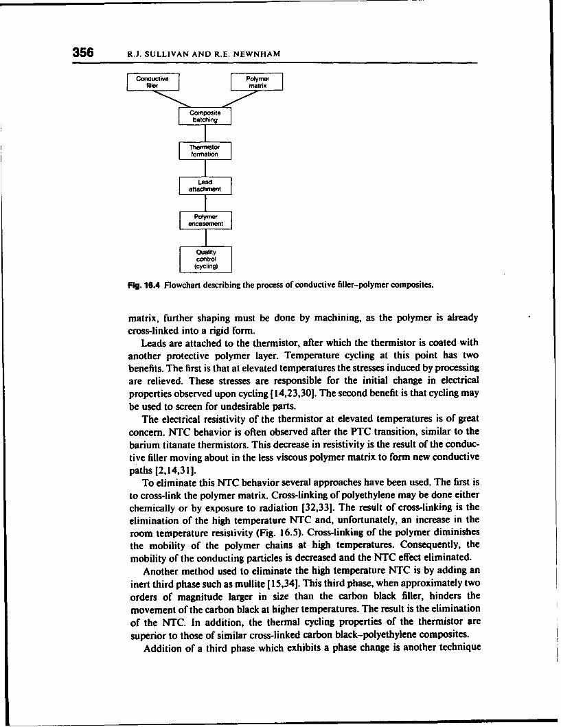
356 R.J. SULLIVAN AND R.E. NEWNHAM
FC.164Fowdc hart deciigteProeso odciele-olymercmpst.
fi frt h matrix
Composite
batching
T hermistor hermistorformation
Lead
attachmentIp olymer l
encasementIcontrol
(cycling)
Fig. 16.4 Flowchart describing the temperaturthe stfiller-polymer composites.
matrix, further shaping must be done by machining, as the polymer is already
cross-linked into a rigid form.
Leads are attached tortit of the thermistor at elevate temprtur is coated withanother protective polymer layer. Temperature cycling at this point has two
benefits. The first is that at elevated temperatures the stresses induced by processing
are relieved. These stresses are responsible for the initial change in electrical
properties observed upon cycling [ 14,2 3,30]. The second benefit is that cycling may
be used to screen for undesirable parts.The electrical resistivity of the thermistor at elevated temperatures is of great
concern. NTC behavior is often observed after the PTC transition, similar to the
barium titanate thermistors. This decrease in resistivity is the result of the conduc-
tive filler moving about in the less viscous polymer matrix to form new conductive
paths [2,14,311].To eliminate this NTC behavior several approaches have been used. The first is
to cross-link the polymer matrix. Cross-linking of polyethylene may be done either
chemically or by exposure to radiation [32,33]. The result of cross-linking is the
elimination of the high temperature NTC and, unfortunately, an increase in the
room temperature resistivity (Fig. 16.5). Cross-linking of the polymer diminishes
the mobility of the polymer chains at high temperatures. Consequently, the
mobility of the conducting particles is decreased and the NTC effect eliminated.
Another method used to eliminate the high temperature NTC is by adding an
inert third phase such as mullite [ 15,34]. This third phase, when approximately two
orders of magnitude larger in size than the carbon black filler, hinders the
movement of the carbon black at higher temperatures. The result is the elimination
of the NTC. In addition, the thermal cycling properties of the thermistor are
superior to those of similar cross-linked carbon black-polyethylene composites.
Addition of a third phase which exhibits a phase change is another technique

COMPOSITE THERMISTORS 357
Wellcrossm-liked
Thermoplatic
fooc
I I I I I i I60 80 100 120 140 160 180
Temperature (C)
Fig. 16.5 Effect of cross-linking on the electrical properties of carbon black- polyethylenecomposite thermistor [321 (DOC, degree of cross-linking).
used to eliminate NTC behavior. Brodeur and associates used pentaerythritol(C5H120 4) as the third phase in a carbon black-polystyrene composite [251.Pentaerythritol has a solid-solid phase transition near 185"C with a latent heat oftransition of 4.13 kJ/mol. In addition to absorbing heat at the solid-solid transi-tion, the particle size of the pentaerythritol (8 ttm) aided in the mechanical stabilityof the composite, similar to the inert mullite phase previously mentioned. As theambient temperature is raised to 185"C, the phase transition in the pentaerythritolabsorbs energy and stabilizes the thermistor temperature at 185"C. The length oftime the thermistor is held at this latch temperature is dependent upon the vol%pentaerythritol in the composite and the heating rate of the sample. For acomposite with 50 vol% pentaerythritol and a heating rate of 6C/min, a delaygreater than 5 min was seen as shown in Fig. 16.6. The NTC behavior is eliminatedbecause the temperature of the samples does not reach a value at which damage tothe sample may occur.
6 Percolation
As the volume fraction of conductive filler in the polymer increases, the resistivityof the composite decreases slightly until at a certain critical volume fraction (V,),the resistivity decreases drastically because of the increased connectivity of the filler(Fig. 16.7). At this volume fraction, conductive chains are formed in the composite.This phenomena is often described using percolation theory. In this case, percola-tion is used to describe the 'richness of interconnects' in the composite thermistor.Many introductions and overviews of percolation may be found in the literature[35-37).
Percolation is often assumed to be one of three types: site, bond or continuumpercolation. Site percolation describes the polymer as a lattice and the filler as being

358 R.J. SULLIVAN AND R.E. NEWNHAM
240----- 15 C-50 Spheres-35 PE
220 -• 15 C-50 Penta-35 PE
200
L£ 10Transition temperature
160.-of pentaeeythritoi
140
120 Melting point of
100.010 o "1 i's 20 25Time (min)
Fig. 16.6 Thermal delay seen for a composition containing 15 vol% carbon black-35 vol%polyethylene-50 vol% pentaerythritol as compared to a composition with 50 vo|% inert mullite
spheres in place of the pentaerythritol.
1010
109
101
10'
10'
10• 10102
10-'
0 10 20 30 40 50 60Filler volume percenti
Fig. 16.7 Percolation curve for a 0.3 mm V203-polystyrene composite system 126]. V, denotesthe volume fraction at which a rapid decrease in resistivity occurs.
randomly added at various lattice sites. If two adjacent sites are filled then theinterface is taken to be conductive. In bond percolation the lattice is completelyoccupied by the filler and there is a finite probability that the 'bond' between twoparticles may (or may not) be conducting 138-40]. Continuum percolation does notinvolve a lattice but rather randomly distributes the filler phase throughout thematrix [41,42].
The value of V. is very dependent upon the filler and polymer selected. Incarbon black-polymer composites it has been shown that VJ, increases as thesurface tension of the polymer increases [43,44]. Sumita et al. attribute this to theinterfacial excess energy (4g) the carbon black introduces to the system and modelit with the following equation 144]:Vc - ZqeRP,( + 3(,ycl/2 - ,YpI/2)2)()

COMPOSITE THERMISTORS 359
Where V. is the critical volume fraction, Ag* the critical interfacial excess energybeyond which the filler coagulates, R the filler radius, and yc and yp the surfacetension of the carbon black and polymer, respectively. This relation is valid whenthe difference between yc and yp is not small due to assumptions made during itsderivation.
Moffatt has shown the contrary to be true for the V20 3 filled polymer system[16]. She saw that as the wetting between the filler and polymer increased, Vc isshifted toward higher values. The increased Vc was attributable to better dispersionof the filler in the systems having superior wetting. The major differences betweenthe two fillers is the particle size and the particle surface energy. In the V20 3-polymer system the relation in Equation 1 is not valid due to a small differencebetween the surface tensions of the filler and polymer, as mentioned above.
Several studies have shown that carbon blacks with small particle size and highsurface area have a lower percolation threshold than other carbon blacks [45-49).This result is also predicted by Equation 1. Similar results have been reported forsystems in which a metal powder is mixed with a polymer powder at roomtemperature and then pressed [50,511. When the polymer particle size was heldconstant, a decrease in the metal powder particle size decreased V,. In this case themetal powder coats the polymer particles. The smaller the metal powder the lessvolume needed to coat the polymer. Kusy showed these trends for the nickel-polyethylene mixture where the particle size of the polymer ranged from 2 to 30times the particles size of the metal [51 ].
Sullivan saw the opposite particle size effect in the V20 3-polystyrene system[26]. Varying the V20 3 particle size from 325 Am down to 0.3 Am increased V,,from 0.04 to 0.34. These results further emphasize the differences between thecarbon black-semicrystalline and conductive filler-amorphous polymer systemsbrought about by the large difference in the filler particle size and surface energy.
In addition, a dependence of Vc on the sample geometry was also shown.Increasing the sample thickness from 0.06 cm to 0.2 cm increased Vc from 0.04 to0.08 for the 325 Am V2 0 3 particle size. This increase was attributed to theincreased difficulty in forming a conductive chain across the thicker sample.
7 Carbon black-semlcrystallne composite themistors
The most widely studied and commercially available composite thermistor systemis that of a carbon black-semicrystalline polymer such as polyethylene. Severalreviews have been written about this system describing processing, possible con-duction mechanisms and filler property effect [52,53]. Doljack describes theproperties and uses of the commercially available carbon black-polyethylene basedPolySwitch® [14]. A PolySwitch® C02R006 thermistor with a low temperatureresistance of 0.042 fl can dissipate 0.95 W of power at an ambient temperature of40"C before switching to the high resistance state. Room temperature resistivitiesof 1-5 fl-cm with PTC magnitudes of six orders have been reported for this type ofthermistor.
The electrical properties are very dependent upon the type of carbon black,polymer, and processing of the thermistor [14,54,55]. Smaller sized (less struc-

360 R.J. SULLIVAN AND R.E. NEWNHAM
tured) carbon blacks exhibit the lowest room temperature resistivity. The magni-tude of the PTC transition also decreases as the size of carbon black decreases.
A polymer with a higher degree of crystallinity exhibits a larger PTC anomaly.Low density polyethylene has a PTC magnitude of 3.5 orders of magnitude while
high density polyethylene has a PTC of 4.5 orders [56]. In addition, a polymer witha narrow melting temperature range has a steep PTC transition [45]. PTC effectsare seldom seen in carbon black-amorphous rubber composites. In these systems
the anomaly occurs only at filler concentrations very near the critical volumefraction [57].
The mechanism responsible for the PTC transition in the carbon black-semicrystalline polymer composites has not been positively identified, though
several models have been proposed. At temperatures below the melting tempera-
ture (Tm) of the polymer, carbon black is excluded from the crystalline polymerregions. This segregation results in a low resistivity composite. At higher tempera-
tures the crystalline regions melt and the polymer matrix becomes less viscous.Rearrangement of the conductive particles into these new amorphous regionsdisrupts the conductive paths and increases the composite resistivity [33,45].
Kohler explains the increase in resistivity as conductive chains being pulledapart by the thermal expansion of the polymer [58]. At the melting temperture adiscontinuous increase in volume would account for the large increase in resistivity.Figure 16.8 shows the increase in volume and resistivity with temperature for a
carbon black-polyethylene composite as reported by DolIjack [14]. The rapid
change in resistance of the thermistor shadows the change in the composite volume,
supporting the views of Kohler.Further support for the importance of the polymer thermal expansion for a PTC
transition was given by Sullivan [26]. Working with the V20 3-polystyrene system
the thermal expansion of the composite above T. was varied by increasing the
6
43 .
3 -
2 1
0-
20 130Temperature (C)
Fig. 16.8 Composite resistivity and volume expansion of the matrix polymer as a function of
temperature for a carbon black-polystyrene thermistor 114]. T.. of polystyrene is approximately130"C.

COMPOSITE THERMISTORS 361
10
* 8- 1
' 6E•"
._• 9
U2-
0*0 200 400 0W 800
Thermal expansion above Tg (ppn)
Fig. 16.9 Dependence of PTC transition magnitude on the composite thermal expansion above
T.. Samples were 30 vol% V20 3-polystyrene irradiated with varying doses of gamma radiation.
Doses of 250 and 50 MRad resulted in thermal expansions of approximately 200 and 700 ppm,
respectively [261.
cross-link density of the polymer. Figure 16.9 shows the dependence of the PTCmagnitude on the thermal expansion of the system.
Two other possible mechanisms involve electron tunneling through a very thin
(<100,k) polymer layer between carbon black particles. Ohn and Natio state thatlarge gaps inlluence [fie resistivity of a conducting chain more thant small gaps 1591.At low !enipteral tires (<'1,,) (fic ivermge gip wi(ldh is small cnouiglhi to Iwrnai(
tunnelintg. Above In, (lhe disliibulion of the gaj widths intilca..s due to somic
particles being pulled apart while others are pushed together. The larger gap widthsresulting from particles moving apart do not allow tunneling, effectively increasingthe chain resistivity. Consequently, the composite resistivity increases.
Meyer assumes that crystalline polymer regions (300 A) separate the conductionparticles [56,60]. Electron tunneling through these regions is easier than tunnelingthrough similar amorphous regions. Consequently, as the crystalline regions melt, theprobability of tunneling decreases and the composite resistivity increases. The NTCbehavior above the PTC transition, Meyer explains, is due to the compressed carbonblack expanding and once again making electrical contact to decrease the resistivity.
8 Conductive fller-amorphous polymer composites
The newest class of thermistor materials are the amorphous polymer based com-posites. Although not seen in carbon black-amorphous polymer composites, a PTCtransition is present in some metal and many conductive oxide-amorphous poly-
mer composites [ 16,18,20,23,24,611. The transition occurs near the glass transition
temperature (Ts) of the polymer.As with the carbon black-polythylene thermistors, selection of the filler is very
important for a low resistivity at room temperature. lFiller resistivity must be less
than the desired composite resistivity. The particle size of the filler is also critical
due to the particle-particle contact resistance [62]. As the particle size decreases,
the number of particles required to form a conducting chain increases, as does the

362 R.J. SULLIVAN AND R.E. NEWNHAM
number of contacts. As a result, the composite resistivity increases.With transition metal oxides such as V20 3, Ti20 3 and V0 2, a low temperature
NTC transition may be incorporated into the thermistor in addition to a somewhat
larger high temperature PTC effect [ 18]. This NTC is associated with the semicon-
ductor to metal phase transition in the filler. The resulting resistivity behavior is asquare well effect as seen in Fig. 16.1.
Hu and co-workers batched V20 3 with polyethylene and epoxy [61]. The PTC
seen in the V20 3-polyethylene composite was very steep (AT= 5C) and occurred
at 130'C (Tmn). The PTC for the V20 3-epoxy composites occurred near 100"C (TS)
and was not as steep (AT= 20"C). The PTC magnitude was 10 and eight orders forthe polyethylene and epoxy systems, respectively.
Littlewood and Briggs report a PTC of greater than five orders for a silver-coatedcopper-epoxy composite [23]. They also report a lower room temperature resistiv-ity with a higher epoxy curing temperature. The higher curing temperature results
in greater internal stresses (greater shrinkage upon curing), which increase thecontact nressure and area between the conductive particles.
9 Dispersion
Composite thermistors show a decrease in the high temperature resistivity with
increasing frequency as shown for the V20 3-polymethylmethacrylate system in
Fig. 16.10 [16]. The origin of this dispersive behavior stems from the relaxation of
polarization mechanisms with increased frequency and has been reported by
several authors [49,63-65].At filler concentrations above Vc and at temperatures below the PTC transition,
no frequency dependence was observed. As the thermistor switches to the high
resistivity state, the conducting particles are presumably separated by an insulating
layer [66,67). This insulating layer controls the conduction of the composite.
los
106
11 1Fg1.10 R20 v01%
freuey dis n 0 i tou Vo102 & 80 Vol%££ i
~55 Vl
101 A a a £&AAUM#~%~ 65 v01%
107 103 104 105
Fr.eaency (kHz)
F~.16.10 Resistivity behavior Of V203-polymethylmethacrylate thermistors showing
frequency dispersion; vol% indicates the volume percent V20 3 167).

COMPOSITE THERMISTORS 363
As the frequency increases, polarization mechanisms in the insulating layerbegin to relax out. Two types of polarization that relax in the frequency range of theexperimental values are space charge (up to 103 Hz) and dipolar (orientational, up
to 109 Hz). Space charge polarization occurs when two materials of unequalconductivity are brought together. This is the result of charge building up at theinterface. Dipolar polarization is due to the rotation of permanent dipoles in anelectric field. As seen in many other systems where inhomogeneity results inbarriers for charge movement, space charge polarization is most important [681.
Maxwell-Wagner theory is used to model this behavior [68,69]. The dielectricconstant (K'), loss (K"), and resistivity (p) are predicted by this theory using the
following equations:
K (K - K -K.(K'=1+ (1 2 T2) 2
K" (K'-K)w (3)1 + 02"g2
F-F0-(Po - P.)(41 = +( + (4)
where
w = frequency (Hz)T= time constant
K' - static dielectric constant
K: - optical dielectric constant
Po - low frequency resistivity (fl-cm)p-, - high frequency resistivity (fL-cm)
Figure 16.11 illustrates the Maxwell-Wagner capacitor model as applied tocomposites. At low frequencies the resistance of the gap (Re) is responsible for thehigh resistivity. At higher frequenc; ,, relaxation of the polarization mechanisms inthe polymer decreases the impedance due to the capacitance of the polymer and asa result, the resistance of the composite is due to the filler resistance (R.) [67].
10 Conduction
Three regions of conduction can be identified on a percolation curve. At lowvolume fraction filler, the composite is resistive and conducts primarily by ionicmovement (impurities) and space charge effects. The filler at this concentration isdispersed throughout the composite at distances too great to facilitate electrontunneling [66].
As the volume fraction increases past Vc, the composite resistivity decreasessharply. In this region the con auction mechanism changes from one of ionicmovement to electron tunneling. At higher fields, -1kctron tunneling may be furtherenhanced by th.-rmal fluctuations. At higher loadings the conductive particles are incontact or separated by only a very thin film of polymer. This results in the lowresistivity [70,71].

364 R.J. SULLIVAN AND R.E. NEWNHAM
Particle
Fig. 16.11 The Maxwell-Wagner capacitor model is applied to the composite thermistor 1671.
Variations in the gap width of the polymer affect the resistivity and type of
conduction [721. An increase in the gap width with temperature would decrease theprobability of electron tunneling and increase the composite resistivity. Sherman etal. modeled the PTC transition behavior with electron tunneling [73]. Their resultspredicted a large PTC transition over a very small filler concentration for thenickel-polyethylene system. Moffatt et al. applied this model to the V20 3-polyethylene and V20 3-epoxy systems [74]. Qualitatively the model predicted thePTC behavior but did not quantitatively fit the data. The probability of thismechanism being responsible for the PTC transition is greatest in the semicrystal-line polymer composite thermistors. These materials have a large volume expan-sion at the melting temperature which could separate conducting particles to thepoint where tunneling across the gap does not occur.
Another possible mechanism for the PTC transition is a decrease in the spacecharge region at T5 or Tm (depending on the polymer matrix) [ 16]. When a polymerand conductor are placed into contact, electrons are injected from the conductorinto the polymer to align the Fermi energies [75,76]. At sufficient loadings (> VJ) thespace charge regions resulting between two conductive filler particles are closeenough to allow conduction across the gap. As the temperature increases through T8
or Tm the number of energy states close to the filler surface that may be occupied byinjected electrons increases. Consequently, the effective gap width increases due tothe electrons not being injected as far into the polvmer 116].
Ionic conduction may also be responsible, i n part, for the PTC transition. At low
temperatures the mobility of impurity ions in the composite is low. At tempera-
tures greater than T. (or Tmn) impurity ions migrate to oppose any applied electric
field. This, in effect, cancels the field in local areas which limits conduction. As a
result, the resistivity increases.

COMPOSITE THERMISTORS 365
11 Summary
PTC thermistors are ideal for applications such as current stabilization, tempera-ture control, and high voltage protection. Until recently, thermistors were manu-factured primarily from ceramics. Developments in composites have producedthermistors with much lower dormant resistivites (1 il-cm) and easier fabricationthan their ceramic counterparts. Because of this, composite thermistors are beingused in applications which require low resistances and cost.
Although the mechanism responsible for the PTC transition is not agreed upon,it has been determined that in the low resistivity (dormant) state the resistivity isdetermined by the conductive filler. In the active, high resistivity, state theresistivity is controlled by the polymer matrix. The mechanism responsible for therapid change in resistance is triggered by the phase transition in the polymer at T.or Tm.
Additions of a third phase or cross-linking have been used to ensure that theproperties of the thermistor do not degrade at high temperatures. The idea behindthese steps is to either prevent the thermistor from reaching elevated temperatures,or limit the motion of the filler particles at these temperatures. These processingsteps have been very successful in stabilizing the electrical properties of thethermistor with repeated cycling.
12 References
I R.F. Blaha. Proceedings of the Electronic Component Conference (197 1).2 J.M. Taylor. US Patent 4,426,633, January 17, 1984.3 P.D. Levett. Ceram Age 83, 44 (1967).4 H.A. Sauer & J.R. Fisher. JAm Ceram Soc 43, 297 (1960).5 W.T. Peria, W.RI Bratschum & R.D. Fenity. JAm Ceram Soc 44, 249 (1961).6 0. Saburi. JAm Ceram Soc 44, 54 (1961).7 V.J. Tennery & R.L Cook. JAm Ceram Soc 44, 187 (1961).8 0. Saburi & K. Wakino. IEEE Trans Compon Parts 53 (1963).
9 B.M. Kulwicki. Adv Ceram 1, Am Ceram Soc, Columbus (1981).10 W. Heywang, JAm Ceram Soc 47, 484 (1964).
11 G.H. Jonker. Adv Ceram 1, Am Ceram Soc, Columbus (1981).12 A. Ruegg, R.S. Perkins & P. Streit. Sci Ceram 11, 559 (1981).13 R.S. Perkins. A. Ruegg. M. Fischer. P. Streit & A. Menth. I.FFE Trans Comln'n Ilt'rids
Manufact Technol 5 (1982).14 F.A. Doljack. IEEE Trans Conilwn Hybrids Alanufact Technol 4, 372 (1981).15 LL Rohlfing, R.E. Newnham, S.M. Pilgrim & J. Runt. J Wave-Mater Interact 3, 273 (1988).16 D. Moffatt. Electrical Properties of V20y-Polymer Composite Thermistors. PhD Dissertation,
The Pennsylvania State University, December (1989).17 F.F.T. De Araujo & H.M. Rosenberg. Proceedings of the 1975 International Conference on
Composite Materials 2, 560 (1975).18 ICA. Hu, J. Runt, A. Safari & RE. Newnham. Ferroelectrics 68, 115 (1986).19 R.R. Singh & R.W. Roberts. Polym Compos 6, 58 (1985).20 R. Matsushita, M. Senna & H. Kuno. J Mater Sci 12, 509 (1977).21 R. Mukhopadhyay, S.K. De & S. Basu. JAppl Polym Sci 20, 2575 (1976).22 S.K. Bhattacharya, S. Basu & S.K De. JAppl Polym Sci 19, 21 (1980).23 S. Littlewood & B.F.N. Briggs. J Phys D: Appl Phys 11, 1457 (1978).24 L Nicodemo, L, Nicolais, G. Romeo & E. Scafora. Polym EngSci 18, 293 (1978).

366 R.i. SULLIVAN AND R.E. NEWNHAM
25 S.A. Brodeur W. Huebner, i.P. Runt & R.E. Newnham. J Mat Res 6, 175 (199 1).26 RiJ. Sullivan. Processing Effects on PTC Composite Thermistors. PhD Dissertation, The
Pennsylvania State University (1991).27 LT. Toy, W.W. Moyer, B.i. Lyons & D.A. Horsma. US Patent 4,388,607, June 14, 1983.28 Li. Middleman, J. Evans & D. Pettengill. US Patent 4,238,812, Dec. 9, 1980.29 S.K Bhattacharya & A.C.D. Chakklader. Polymn Plast Technol Eng 19, 21 (1982).30 V.E Gui', 1-7 Shenfil', G.K Mel'nikova & N.L Maslennikova. Soy Plast (Eng Transl) 4, 46
(1966).33 P.V. VanKonynenburg, A. Au, C. Rauwendaal & A.J. Gotcher. US Patent 4,237,441,
December 2, 1980.32 M. Narkis, A. Ramn & Z- Stein. J Appi Polym Sci 25, 1515 (1980).33 M. Narkis, A. Ram & Z. Stein. Polymn Eng Sci 21, 1049 (198 1).34 L.L Rohifing, S.M. Pilgrim, R.E. Newnham & J. Runt. J Wave-Mater Interact 3, 301 (1988).35 D. Stauffer. Introduction to Percolation Theory. Taylor & Francis, London (1985).36 V.K.S. Shante & S. Kirlpatrick. Adv Phys 20, 235 (197 1).37 R. Zallen. The Physics ofAmorphous Solids. Wiley, New York (1983).38 V.A. Vyssotsky, S.B. Gordon, H.L Frisch & J.M- Hammersley. Phys Rev 123, 5, (196 1).39 M. Nakamura & M. Mizuno. J Phys C: Solid State Phys 15, 5979 (1982).40 H. Scher & R. Zallen. J Chem Phys 53, 3759 (1970).41 S. Lee, Y. Song, T.W. Nob, X. Chen & J.R. Gaines. Phys Rev B 34, 10 (1986).42 1. Balberg. Philos Mag B 56, 991 (1987).43 X. Miyasaka, K. Watanabe, E. Jojima, H. Aida, M. Sumita & K. Ishikawa. J Mater Sci 17,
1610 (1982).44 M. Sumita, S. Asai, N. Miyadera, E, Jojima & K. Miyasaka. Colloid Polym Sci 264, 212
(1986).45 A. Voet. Rubber Chem Technol 54, 42 (1980).46 C. Kiason & J. Kubat. Int J Polym Mater 11, 47 (1985).47 E.O. Forster. IEEE Trans Power Appar Syst 90, 913 (197 1).48 M. Narkis & A. Vaxman. J Appl Polymn Sci 29, 1539 (1984).49 L Benguigui, J. Yacubowicz & M. Narkis. J Polym Sci 25, 127 (1987).50 A. Malliaris & D.T. Turner. J AppI Phys 42, 614 (197 1).51 R.P. Kusy. JAppl Phys 48, 5301 (1977).52 T.M. Aminabhavi, P.E. Cassidy & C.M. Thompson. Rubber C/hrn Technol 63, 451 (1975).53 F. Carmona. Ann Chim Fr 13, 395 (1988).54 C. Kiason & J. Kubat. J Appl Polymn Sd 19, 831 (1975).55 E.V. Harris, F.E Jones & F.C. Church. Cabot Technical Report RG- 130.56 J. Meyer. Polym Eng Sci 13, 462 (1973).57 D. Wolfer. Eur Rubber J 159, 16 (1977).58 F. Kohler. US Patent 3,243,753 (1966).59 K. Ohn & Y. Natio. J Appi Phys Jap 10, 99 (197 1).60 i. Meyer. Polyrn Eng Sci 14, 706 (1974).61 K.A. Hu, D. Moffatt, J. Runt, A. Safari & ILE Newuhain. J Am Ceram Soc 70, 583 (1987).62 G.R. Ruschau, S. Yoshikawa & R.E. Newnham. Int J Hybrid Microelectron 13, 100 (1990).63 K.T. Chung, A. Sabo & A.P. Pica. J App) Phys 53, 6867 (1982).64 F. Bueche. J Appi PhysM4, 532 (1973).65 F. Bueche. J Polym Sci 11, 1319 (1973).66 A.I. Medalia. Rubber Chem Technol 59, 432 (1986).67 H. Kawamoto. Carbon Black-Polymer Composites. Marcel Dekker, New York, Ch. 5 (1982).68 F. Bunget & M. Popescu. Physics of Solid Dielectrics, Materials Science Monographs 19.
Elsevier, New York (1984).69 A. Von Hippel. Dielectrics and Waves. Wiley, New York, (1954).70 R.M. Scanisbrick. J Phys D: App) Phys 6, 2098 (1973).

COMPOSITE THERMISTORS 367
71 F.J. Balta Calleja, T.A. Ezquerra, D.R, Rueda & J. Alonso-Lopex. J Mater Sci Lett 3, 165(1984).
72 A.K. Sichel, J.L. Gittleman & P. Sheng. J Electron Mater 11, 699 (1982).73 R.D. Sherman, L.M. Middleman & S.M. Jacobs. Polym Eng Sci 23, 36 (1983).74 D.M. Moffatt, J.P. Runt, A. Halliyal & RE. Newnham. J Mater Sci 24, 609 (1989).75 F.J. Blatt. Physics of Electronic Conduction in Solids. McGraw-Hill, New York (1968).76 A.R. Blythe. Electrical Properties of Polymers. Cambridge University Press, Cambridge
(1979).

APPENDIX 27

PROCEEDING, Electronic Components and Technology Conference,San Diego, Ca, Ray 18-20, 1992
Percolation Constraints in the Use of Conductor-Filled Polymersfor Interconnects
G.R. Ruschau. S. Yoshikawa. and R.E.Newnhazn
Materials Research Laboratory
Pennsylvania State University
University Park. PA 16802
AnfTaACTConductor-filled polymers are used in the microelectronics
industry for conductive epoxies. solderless interconnects, andelectrode contacts. The electrical properties of these materials aredescribed by conventional percolation theory, which states that at acertain critical volume fraction of conductive filler, the compositetransforms from an insulator to a conductor. due to the formation ofthe first continuous chain of filler panicles.
However. theoretical percolation predictions ignore the "Wrealities encountered in the electronic fabrication. While percolation
models involve statistical probabilities based on randomly-filledisometric matrices, the filling of polymeric materials withconductive filler is far from random. and the geometry of theconductive pattern is far from isometric.
In this investigation, the electrical properties of Ag-filled 0 vcsilicone rubber composites were studied with an emphasis on the VOLUME FRACTION FILLERproperties of thin. flexible sheet-type samples. It was found that thecritical volume fraction for conduction for a given composite system Figure 1: Percolation theory as applied to conductive composites.was highly dependent on the measurement geometry for a given showing the development of conductive pathways withcomposite component. As a consequence. the resistivity across thincomposite tapes differed from the resistivity through the thickness an increase in volumefraction offiller.of the tape. In some extreme cases, composites were insulators inone direction and conductors in another directiong coordination, as shown in Table 1. V,'s are given for both two-
The two important variables in deciding the degree of dimensional and three-dimensional systems: despite the variationsanisotropy in conduction are the geometry factor. G (=area of in lattice packing, all V.'s are roughly equivalent within both sets ofelectrode contact/distance between electrodes) and r. the ratio of the numbers.particle size to the smallest sample dimension. As G and r The predicted V, for different packing geometries variesincreased, the percolation probabilities deviated from bulk samplesot the !.ime composite. A Monte Carlo- type computer simulationof the random filling of geometrically anisotropic matrices verified Table !: Critical volume fractions concentrations for bond (pcbo'd)that the variation in critical volume fraction with G and r in and site (pcSe) percolation on a variety of lattices,18 1
otherwise identical compositions was an expected result, followingthe lj%%N of statistical probability. Thus. when formulatingconductive composite compositions. the critical volume fraction for Lattice Lae Maximum i,.pcsateconduction is characteristic of a given system only for small values Type pcbmd psite oordinatoi Packing ,=of G and r.
When the geometric restrictions are minimized, the critical% olume fraction for conduction can be estimated by considering theloose packing density of the filler powder. In this way, conductive triangular 0.347 0.500 6 0.907 0.450composites may be thought of as a conductive skeleton of a certain square 0.500 0.593 4 0.785 0.470packing geometry rather than as a randomly filled particle matrix. kagome 0.450 0.653 4 0.680 0.440
honeycomb 0.653 0.698 3 0.605 0.420
INTRODUCTIONComposites consisting of highly conductive filler powder 3Qiuioui
dispersed in a flexible. insulating polymer matrix are commonly F terdused in electronic applications for die attachl t l, solderless cu-c01n1.4 1connectorsl 2l. thermistorsl3-41, and pressure sensing elements1 51 . cubic 0.119 0.198 12 0.741 0.147Other uses of such composites include electromagnetic shielding Body-centeredand anti-static devicesl61 as well as chemical sensorsl,). cubic 0.179 0.245 8 0.680 0.167
The properties of composite systems are understood interms of percolation phenomena: when a sufficient amount of Simple cubic 0.247 0.311 6 0,524 0.163conductive filler is loaded into an insulating polymer matrix, thecomposite transforms from and insulator to a conductor, the result Diamond 0.338 0.428 4 0:340 0.146of continuous linkages of filler particles (See Figure I). The critical Random cubic --- 0.2 --- 0.637 0.160volume fraction at which this transformation occurs. V,. is the focusof this investigation.
For percolation in a model system, V. has been predicted *empirically derivedfor different packing geometries as a function of the lattice
481 0569.5503/92/0000-0481 $3.00 *1992 IEEE

slightly depending on the type of percolation assumed. "Site" used. After weighing all samples to the proper volume loadingpercolation assumes that the Is sites are randomly filled until a using a mixture of about 16% silicone in tnchloroethylene (TCE)continuous linkage is formed. continuity is assumed when adjacent solvent the batches were mixed for one minute with a polyethylenelattice sites are filled. "Bond" percolation assumes that the lattice propeller blade at 800 rpm.sites are filled but that adjacent lattice sites do not necessarily form a Approximately 20% excess TCE was added to obtain thecontiunuous linkage, but rather are randomly bonded (electrically proper viscosity (-10.000 CPS) for tape casting. The slip was castcontacted in this case) as more filler is loaded into the matrix, onto 6"x8" borosilicate glass sheets using a doctor blade thicknessPredicted Vc's for site percolation are generally higher than for bond of 1.5mm. which resulted in a final sample thickness of 0.25-percolation: percolation in real systems is thought to be a mixture of 0.30mm. After air drying for 4 hours, the samples were cured atboth site and bond percolation. 1800C for 2 hours then removed from the glass sheets with a razor
One problem with the predicted Vc's is that real systems blade and cut into 2cm x 5cm rectangular samples.Percolation was verified by measuring the d.c. electrical
seldom follow these rules of lattice packing and percolation: resistance of three to six samples of each formulation and thicknesssystems which show V, in the range of 15-17% (the predicted range was measured across each sample by a 4-probe measurementfrom Table I) are no more prevalent than systems showing much technique using gold-plated leads and a digital multimeter.higher V,'s. This makes it difficult to produce experimental results Percolation was assumed when the resistivity was closer to theto which an appropriate mathematical model can be applied. Table 2 resistivity of the filler material (ranging from 10.6 to 10-t Q-cmM
than to the resistivity of the silicone rubber (10CQ-cm). SEManalysis was used to verify the random dispersion of the filler
Table 2: Crntical volume fracntons for conductive composite within the system.systems by other investigators. In order to determine the scaling effects on model
percolation systems. critical volume fraction variations with samplegeometry and particle size were calculated for a square lattice using a
Filler Polymer Vc Reference two-dimensional Monte Carlo-type program. written in BASIClanguage. All simulations were performed on a Macintosh SEcomputer.
Cu Polyvinylchloride .01 [9] The basic parts of the program were as follows:Cu Polyvinylchloride .20 [10] 1. The desired dimensions of the overall sample (vertical andCu Polystyrene .15 [11] horizontal lengths of a rectangle) were entered.Cu Polystyrene .35 [111 2. The desired filler "particle" size was entered.
3. An internal random number generator was used to randomlyselect a lattice site and place a "particle" on that lattice site: the output
Ag Polystyrene .36 [121 ]was displayed graphically on screen.Ag Rigid Epoxy .09 (131 4. After filling a lattice site. the program automatically checked forAg Rigid Epoxy .30 114] percolation in the vertical direction. If the system was percolated.Ag Silicone Rubber .15 [14] the critical volume percent (actually. an area percent since theAg Silicone Rubber .27 [151 program was two-dimensional) was calculated by the following:
V,(%) = (,t/4) W#filled lattice sites) x 100% (1)Sb:SnO2 Flexible Epoxy .30 [161 (total # lattice sites)Sb:SnO2 Flexible Epoxy .,4O 1161
5. If percolation was not detected, more lattice sites were filled until
Fe Styrene / acrylonitrile .20 (17] percolation was detected.
Al Styrene / acrylonitrile .40 [17] 6. After recording the critical volume percent. the program wasrepeated with the same parameters for a total of twenty separatesimulations for each geometry and particle size variation.
lists V. for a number of conductor-filled polymers studied by other This computer simulation was very similar to the traditionalinvestigators. showing how Vc can vary even within the same Monte Carlo statistical analyses of random processes. although the
graphics output and percolation detection algorithm were limited tofiller/polymer system. two-dimensional simulations only.
An important limitation on the predicted V,'s is that the The packing densities for all fillers used were measuredprobability of percolation must be the same in all directions. i.e.. the using a 10 cc graduated cylinder with 0.1 cc graduations.overall lattice in the two-dimensional case is a square. and the Approximately 5 cc of the powder was weighed in the cylinder, thenoverall lattice in the three-dimensional case is a cube. For caused to settle by rattling the cylinder lightly on the counter top formicroelectronic applications, the focus is nearly always on sample 30 seconds (approximately 500 "taps") to simulate the techniquegeometries in which at least one dimension is exaggerated relative to used commercially for tap density measurements. The volume ofthe other dimensions, such as thin sheets or wires. The scaling the settled powder was estimated to the nearest 0.05 cc. Thus thefactors involved in this type of percolation throw another variable packing fraction. $, was calculated by the formula:into the system.
In this investigation, we concentrate on the properties ofsome silver-filled silicone rubber composites, and show how the #P = (wW'')I Of t2)artificial percolation restrictions effect both the critical volumefraction and resistivity of the composite. A computer simulation of where wr = measured weight of powder samplethe two dimensional case shows that these restrictions effect Vc in a V, = volume of tapped powderpredictable manner. An empirical method to predict Vc for non- pr= theoretical density of filler powderrestricted systems is presented.
EXPERIMENTAL PROCEDURE RESULTS AND DISCUSSIONSilicone rubber (G.E. 845 silicone elastomer) was the A Geometry Ratio&
matrix material used in this investigation. Relatively monosize Figure 2 illustrates (with 9.0 pm Ag powder-, illed siliconedistributions (±10%) of each of the conductive filler powders were rubber) how V. can vary with sample thickness (which was varied
482

I013 L was a constant (2.5 cm) and A = (sample thickness x width., •.2. where width=1.5 cm). The sample thickness varied from 50 pim to10- 1 1 250 prm. so the overall geometry factor varied from 0.0024 cm to
I 109 00.0150 cm. Geometry factors less than 1.0 cm may be termed as0 7 dec'easing "unfavorable" geometries for percolation. especially when I is*,10 thickness s t - 65 urn small.S01 5' " t - 100urp0 4% w t. Conversely. geometries with G > 1.0 cm may be termed as
" 0 : t m '50 o•n "favorable" geometries for percolation. This implies that the0 1001 o t - 0rn samples in Figure 3 would show very different behavior if.* 0o measured through the thickness rather than across the thickness.I 102 Figure 4 shows the variation in V, for the samples in Figure 3 as the
10-3o10410"
0 10 20 30 3CVeluame 2 Al [ 9C rn A
Figure 2: Percolation curves (with mathematical curve fits) for 0A9.0 pm Ag powder.filled silicone rubber composites. 20T
47by casting with different doctor blades) for otherwise identical a,samples. While the thickest samples appear to percolate at -18 iovol%. the thinnest samples require more filler to reach a low Iresistivity. This effect is much less pronounced in Figure 3. which
10 i•0112 001 0! I I
1010 Geometry Factor. cm
O 107 decreasing * t-65 urm Figure 4: Variation in Vc for the samples shown in Figures 2 and.106 thiickness ~t 0 r,* 10 5 ,N tc1nesU 3 as a function of geometry factor.
103 a t-150 um geometry factor goes from unfavorable to favorable for percolation.,• ,0 •o t-300 lim--u With G > 1. a small r becomes more favorable for percolation.
102:3 0 2 B. Monte Carlo Simulation10 N . L.__ Monte Carlo percolation simulations. in which a lattice of a
0 10 20 30 given geometry is filled randomly, are useful due to their ability tovoliume Al generate an accurate distribution of percolation probabilities. In this
case. a Monte Carlo-type algorithm was used to illustrate whatFigure 3: Percolation curves I with mathematical curve fits) for happens to percolation probabilities for a square lattice when G and
0.5 pm Ag powder-filled silicone rubber composites. the r are altered.Figure 5 is an example of the graphics of the program
output for the Monte Carlo algorithm, with percolation checkedshows the same thickness variations for 0.5 pim Ag powder-filled between the cross-hatched "electrodes" for each simulation. Sincesilicone rubber.
This same trend was seen repeatedly in samples of other _ _ _R__ _A__ _ _ _
compositions. As the average particle size (d) decreased relative to
the sample thickness (t) the limitations imposed by sample (egeometry were not as severe. When one dimension of the samplewas the same order of magnitude as the particle size. the greatestvariation in properties occurred. In terms of site percolation. theprobability of continuing a percolation path (i.e.. filling an adjacentlattice site) was always greater for a particle in the bulk of thecomposite than for a particle at the surface. simply because there
were more possible directions (i.e.. more adjacent lattice sites) forthe path to continue. The larger the particle size relative to thesample thickness (or the lower the t/d ratio, which we call n). the (b) [c)greater the percentage of particles occupying positions at the Figure5: Graphics outpufrom the Monte Carlo percolationsurfaces. simulation for (a)favorable percolation geometry
Clearly. the overall geometric factor for the resistivity (G=5.O). (b) neutral geometry (G=I.0), and (c)calculation was the most important number to consider. This urlfavorable percoiation geometry (G-0.2).geometric factor, G. for any sample is given by:
G = A/L (3) the program was a two-dimensional simulation only, the geometryfactor was the vertical dimension of the "sample" divided by the
where A is the effective electrode area. and L is the distance horizontal dimension.between the electrodes. For samples such as those in Figs. 2 and 3. Figure 6 shows the calculated two-dimensional critical
483

volume fractions (actually, critical area fractions for two C. Geometry Effect on Resitivitydimensions) as a function of (a) F. and (b) G. Clearly. as the As shown in the previous section. G and r can have a
profound effect on the measured properties of a composite samplebecause of the inhomogeneous nature of the composite. The choice
(a) of direction across which the electrical resistivity is measured can80 •determine if a composite appears to be an insulator or a conductor.
Thus. sometimes sample resistivities are not directly comparable.60- •These data are readily explained by considering the gener~d
0G-27,0 behavior of a composite near the percolation threshold. Figure 7
-- w- 6-2.540 -- G-I 0
0
-- -04 R
20 -o G-0 0.a
0 01 10 1-00 1000 uJ
rk cc ; <=1. 01 .-- GEOMETRY
(b) a VW 6 1 FACTOR
" '0"".j" - -VOLUME FRACTION FILLER
40 Figure 7: Qualitanve representation of the percolation behavior of-r-2 composites as afunction of the geometry factor.
*. ---.-- 1--s illustrating the effects of a shift in Vc on the resistiviryS---a--- rro for a given volume fraction of filler.
20 - -- rwS4
illustrates the percolation curve for a typical composite as a functionof G. The resistivity drops sharply when percolation first occurs.
0 0 At the base of the percolation threshold, there is a broad region inGeoetr Fawhich the connectivity is incomplete. It is in this region that6re,.rry Fucta- samples with smaller r were often found: thus potentially low
Figure 6: Results from the two-dimensional Monte Carlo y samples are limied by the incomplete percolation.
percolation simulation of V, as afwiction of(a) the D. Packing Fractions. Morholorv. and VLparticle sizelsample thickness ratio. r. and (b) te Even if G=1 and r is large. V, is rarely in the predictedgeometry factor. G. range of 14-17%. Janzen first introduced the notion that critical
volume fractions could not be adequately treated by traditionalpercolation theory (even for isotropic matrices), in which perfect
geometry factor increases, the critical volume fractions increase for spheres arranged in ideal packing geometries are assumed.l8ll Heall r. with the most dramatic changes occurring for low r (relatively proposed that V, for carbon black-filled polymers used a anti-static
large particles in thin samples. which is the case in Fig. 2. As r mats must be related to the specific void space for a pure fillerincreases, as indicated in Fig. 6(b). the curves for all the geometic material, that is. the ability (or inability) of a filler to pack m a certainfactors converge to a value near 47%. which is the predicted V, for density. Thus the critical volume fraction for a certain filler materialthe square lattice from Table 1. Similar trends would be expected can be estimated by imowing this variation.for a Monte Carlo simulation of the three-dimensional can, wih the Table 3 lists the results of the measured packing fractions.predicted V,'s converging to the value of 16.3% for simple cubic op. and the observed critical volume fractions for a number of Agpacking. and Ag-coated powders investigated, along with average particle
It was also interesting to note that the standard deviation in sizes. A very good correlation between 4h and V= was observed forthe dam consistently decreased as r increased: this was consistent all samples: V was normally about 0.05 below $,. Thus.with the theory of statistics. which implies that higher accuracy is sa mpls:tws may bout 0.05 below s .always obtained when the sampling lot (in this case. the number of conductive composites may be thought of as a conductive skeletonlattice sites) is greater. This also had implications for the ofeatcertain packing latce: this packing laice is the distinguishingreproducibility behavior of many of the samples; reproducibility Fgur e f shows the relationship between p and particle sizeimproved as r increased and as 0-->l. for polygonal AS powders of a narrow size distribution, and very
The predicted critical volume fractions in Table I assume spherical AS-coated powders of a narrow size distribution: Vcnot only specific packing geometries, but also assume that each values were left off for c ofrity. The d in both casie is the same:sytmpercolates in all directions with equal probability. In all vle eelf f o lrt.Teaedi ohcssi h aesystem p l ilrsmaller particles pack less densely than larger particles, and as suchcases, the overall lattice must have GO 1.0. In practice. therefore."the" critical volume fraction for conduction in a conductor-filled result in lower V€ when composites ae formulatd (as indicaed bypolymer can be compared to the predicted values in Table 1 only the data in Table 3). The actual 4 values for the polygonal powders
when cube-shaped samples are measured, in which G=1.0. and are not comparable to $p for spherical powders. however. Sphereswhen r is very large. tend to pack much more densely than the more irregularly-shaped
484

Table); Pac~ing fractions and critical volwinefracnons for Ag andAg-coatedffier in silicone rubber.
Filler Avg. Particle %i ObservedSize. Pnv
PolygonalpowderAge 0.5 0.07 0.05
Agf 4.0 0.17 0.16 Z. SmallAllt 5.0 0.22 0.15 R fmlrf ATILAll 9.0 0.27 0.20 0\ PALTICLE~
Ag:TiO2o 1.0 0.19 0.15 VOLUME FRACTION FILLERAg:Ni* 5.0 0.31 0.25
Ag:Phenolic Resinn 5.0 0.29 0.25Ag:Ptienolic Resino 12.0 0.39 0.30 Figure 9: Qualitative representation of tile Percolation behavior ofAg:Phenivlic Resin" 15.0 0.46 0.0composites of identical chemnical cornpjosition butAg:Phenolic Resirr 35.0 0.56 0.50 varying particle size.
*Metz Metallurgical Corp.mMitsubishi Metal Corp. CONCLUSIONS
I* Novamnet Snecixah Products Corp. Critical volume fractions for one conductor/polymer systemcan be compared to another system only when a neutral geometry ismeasured, and when the rfller particle size is very small relative toany one dimension of the sample. minimizing r also minimizes the
07- effects of sample geometry. As G--> I and r increases, the
0.--random cubic paCk ing 1+1 reproducibility improves and V, can be estimated by measuring thepacking fraction of the loose filler material. The rules of particle
05 pecui acw packing then apply to composites. and trends in V, with filler
I .# variation can be predicted. In the same way that sample geometrySod *..igrestrictions affected V,. the same restrictions affected resistivity.
Samples with small geometry factors tended to have larger0.3 resistivities. particularly when r was relatively larg.
I302- Thus, when considering the use of conductor-filled110 .8ACOTDSPHERES polymers for electrical interconnects, in which the geometry of the
o POY0A AgPWDR conductor is often specified by circuit design, the size and
00 1 40I morphology of the conductive filler material should be chosen0 to 20 3 40specifically for the application. Fine particle sizes produce the most
Aver" Prtile Sze.psageometry-independent samples for these applications, but when theAvu-ge Prt~ce S~e. ~lowest possible resistivity is desired, there is an optimum particle
Figure&8 Measured packing fractions for spherical and size for the stated geometry.polygonalfillers as afuinction of average particle size.
REFERENCES1. R.L. Op"la and J.D.Sinclair. "Electrical Resistvity of Silver-
polygonal powders. Non-spherical powders normally show a Filleid Epoxies for Die An-nab." Ann.ProcReliahPhvst qgreater tendency for "bridging" in compacts. Bridging led to lower 23. 164 (1985).packing densities and lower V, in all cases. This bridging is Z G.E. Pike. "Electrical Properties of Conducting Elastoaners."especially significant when fibers and flakes are used as fillers. UnfdkiLUdI3hj&&R 81-0263 (19081).
This was consistent with the theory of particle pecking.(191 3. K.A. Hu. D.Moffatt. J.Runt. A.Safari. and R.E.Newnham.Packing density decreases with smaller particle size due to an "V2 0-Polyme~r Composite Thernistors.* LLA.Cr.oL 70.increase in surface area, lower particle mass, and a greater 583-585 (1987).significance of the weak short-range forces. These short range 4. L.L. Rohlfig, R.E.Newnham. S.M.PIlgrim. and J.Runt.forces include electrostatic fields and surface adsorption of moisture "Mutikphase Composite PTC Thermistors." L-WaxeMad-Ini.and other wetting liquids leading to agglomeration. 3. 273-281 (1988).
An additional effect was the shifting in V. to lower volume 5. S. Yoshikawa. T.Ota. and R.E.Newnham. "Piezoresistivity infractions which occurred when the particle size was decreased. as PoyerCrai Copoies"M)3.23illustrated in Figure 9. Near V, for a coarse filler. the same volume 267 (1990. Satcay.hSLEUZLM M m-ekfraction filler will produce lower resistivity composites with fine Ne York. 19aa 86ry. aiIhlnm MrelDkpowders. As the volume fraction of filler is increased beyond the 7. OR. Ruschau. R.E.Newnham. i.Runt, and B.E.Smith. "0-3V, region. the coarse fires will eventually produce lower resistivity Ceramic-Polymer Composite Ciemical Sensors." Ses aAtcomposites. The reasons for this 12DI will not be described here. 20. 269-275 (1989).
485

& Zallen. R.. The Phvsics of Amohous Solids Wiley, NewYork. 1983.
9. Das. D.. S. Basu, and A. Paul, "PVC-Cu Composites withChemically Deposited Ultrfme Copper Particles." JMaLSi.15. 1719-1723 (1980).
10. Bhanacharya. SK.. S. Basu. and S.K. De. "Effect ofTemperature on the Electrical Conductivity of Poly(vinylChloride)-Copper Composites," J.AgR2.Pol.Sci, 25. 111 -118(1980).
11. Pierre. C.. R. Deltour. AJ. Perenboom. and P.J.M. VanBentum. "Electrical Conduction Mechanisms in Polymer-Copper Particle Composites. I.Temperature and High-magneticField Dependence of the Conductivity." PhxLRex4 , 42. 3380-3385 (1990).
12. Matsushita. R.. M. Senna. H. Kuno. "Electrical Resistivity ofHot-Pressed Silver-Polystyrene Powder Mixture," J.MaZt.Sci12. 509-516 (1977).
13. Pujol. J.M.. C. Prud'homme. M.E. Quenneson. and R. Cassat."Electroconductive Adhesives: Comparison of Three DifferentPolymer Matrices. Epoxy. Polyimide, and Silicone." J.Adhes.27. 213-229 (1989).
14. Schoch. K.F.. and A.I. Bennett. "Electrical Evaluation ofConductive Adhesives." IEEE L., 291-293 (1985).
15. Miller. B.. "Polymerization Behavior of Silver-Filled EpoxyResins by Resistivity Measurements." J.Apnp.Polv.Sci. 10.217-228 (1966).
16. Ota. T.. I. Yamai. J. Takahashi. S. Yoshikawa. and R.E.Newnham. "Effects of Filler Particle Size on the ElectricalResistance of Conductor-Polymer Composites." presented atthe Second International Ceramic Science and TechnologyCongress. 1990.
17. Nicodemo. L.L. Nicolais. G. Romeo. and E. Scafora."Temperature Effect on the Electrical Resistivity ofMetal/Polymer Composites." Polymer Eno. and Sci. 18. 293-298 (1978).
18. Janzen. I.. "On the Critical Conductive Filler Loading inAntistatic Composites." L.AMpl.Phys. 46. 966-968 (1975).
19. German. R.M.. Particle Packin. Characteristics, Metal PowdersIndustries Federation. Princeton. NJ.. 1989.
20. Ruschau. G.R.. and R.E.Newnham. "Critical Volume Fractionsin Conductive Composites." L.,mLMati. in press.
486

APPENDIX 28

The Volume Fraction and Temperature
Dependence of the Resistivity in Carbon Black
and Graphite Polymer Composites: An Effective
Media - Percolation Approach
Michael Blaszkiewicz, David S. McLachlan*, andRobert E. Newnham
Materials Research Laboratory,
The Pennsylvania State University,
University Park, Pa 16802.
Permanent address: Department of Physics,
University of the Witwatersrand,
Johannesburg, South Africa

STRACT
A quantitative general effective media (GEM) equation is used to describe a
broad range of experimental resistivity-volume fraction results for graphite-
polymer and carbon black-polymer composites. The parameters used are the
resistivities of each component and the two percolation morphology
parameters, a critical volume fraction, 4c, and an exponent, t. A preliminary
model, also based on the GEM equation, is used to describe the temperature
variation of the resistivity of the diphasic material near the critical volume
fraction.

INTROUCTI1
Since the 1930's carbon black fillers in resistive polymer matrices have
been used to make commercial conductive and antistatic compounds.1 The
resistivity of the diphasic composites varies as a function of the volume fraction
of the conducting material. A resistivity-volume fraction graph has three major
regions: (1) the low-loading region of carbon black in which the resistivity of the
polymer dominates, (2) the percolation region where a small increase in the
loading can bring about a large decrease in the resistivity of the composite, and
(3) the high loading region of carbon black in which the resistivity approaches
'hat of carbon black.2
THE GENERAL EFFECTIVE MEDIA fGEM) EQUATION
Considerable experimental and theoretical work has been done to
examine and to explain how the volume fractions and the morphology of the
components affect the electrical behavior of the composite materials (see for
example Reference 2). Previous theoretical work has relied on percolation and
effective media theories. Percolation theory3.4 is limited in that it is valid only
when the ratios of the resistivities of the two components are infinite.5 This can
be a problem when dealing with real systems where all components have finite
resistivities.
Effective media theories4 are used to try to predict the effective or large-
volume average of the electrical conductivity, dielectric constant, thermal
conductivity, gaseous diffusion, and magnetic permeability of composites.
There are two special cases for which effective media theories exist, the

2
symmetric and asymmetric cases.4 The symmetric case assumes that a random
mixture of spherical (oriented ellipsoidal) particles of two (or more) components
completely fill all space. In the asymmetric case the surfaces of the particles of
one component (the filler) are always completely covered by the other
component (the matrix). The filler or particle sizes are assumed to have an
infinite range in the derivation of both theories. When one component is a
perfect insulator, the symmetric media theory contains a conductor-insulator
transition at a specific conductor volume fraction, which depends on the shape
of the particles, whereas the asymmetric theory does not.4 In practice,
conductor-insulator transitions occur over a wide range of volume (or area in
two dimensions) fractions (see for instance References 6-11).
A generalized effective media (GEM) equation with two morphology
parameters, Oc and t, has been proposed by McLachlan. 6 It was derived as an
interpolation between the symmetric and asymmetric effective media theories.
The GEM equation written in terms of electrical conductivity is:
+ - 0
CY Yt + Y~at CY t + __ 1aS1 (Y2 m h (. (1)
where 0 is the volume fraction of the high conductivity component, and
Oc = 1 - fc is the critical volume fraction of the high conductivity component at
which a percolation path is formed through the media by the high conductivity
component. Here, al is the conductivity of the low conductivity component, Ch is
the conductivity of the high conductivity component, am is the conductivity of the
medium itself, and t is an exponent. Equation 1 reduces to the symmetric and

3
asymmetric theories and has the mathematical form of the percolation equation
in the appropriate limits. 6
The GEM equation can also be viewed as a matched asymptotic
expression as it interpolates between the two percolation equations given
below. When al = 0, the GEM equation reduces to:
m = Ch ( -fIfc)t (2)
and when oh = Ph, Ph = 1/01, Pi = 1/0h it becomes:
Pm = Ph (1- 0 / O)t (3)
where the critical volume fraction is Oc = 1 - fc and where $ = 1 - f. This is
illustrated in Fig. 1 where Eqs. 1, 2, and 3 are plotted for the typical three
dimensional morphology parameters fc = 0.84 (Oc = 0.16) and t = 1.7 with ah = 1
= P1 and ag = 10-6 or Ph = 106. This figure clearly indicates where the percolation
equations will not suffice and the GEM equation must be used.
When fc = 1 or Oc = 1 equations (2) and (3) are both forms of the
Bruggeman asymmetric equation 4 which allows values for L, L', m, and m' to be
calculated from the corresponding exponent in the asymmetric media theory
[6,12,13], which gives:
L = 1 - fc /t, LU = fc /t, m = t /fc, m'= t /fc. (4)
Values of m and m' as functions of the demagnetization coefficient Lc * (Lb = La)
calculated for ac = 0 and 0 h = -•, respectively, from equation (23) in Reference
13, are plotted in Reference 6.

4
The GEM equation has been used to accurately fit a vast amount of
conductivity data.6-11 It has also been used to fit the electrical and thermal
conductivities, and the experimental permeability data from a series of sintered
nickel samples (0.14 - 0.95 volume fraction of nickel) while using the same two
morphology parameters, fc and t.7
This article reports how the GEM equation was used to quantitatively fit
the resistivity versus volume fraction data for carbon black-eccogel and
graphite-eccogel composites. Also, the temperature coefficient of resistivity for
a 47 volume percent graphite sample was modelled using the GEM equation.
FITTING PROCEDURE
The experimental resistivity vs. volume fraction data for the graphite- and
for the carbon black (Vulcan XC-72R)- eccogel (1365-0) epoxy systems 14 were
fitted to the GEM equation. The parameters fc, t, Ph (the resistivity of the
polymer) = 1 / q1, and pi (the resistivity of the conductive filler) = 1 / Oh were
varied freely. The computer program uses an IMSL non-linear regression fitting
program, the experimental conductivity (volume fraction) and the variable
parameters to calculate a volume fraction (conductivity) called Calc from Eq.1.
Calc is then compared to the actual volume fraction (conductivity) called Expt.
The sum of the squares of the residuals, called SSQ:
SSQ = y, [(Calc - Expt)]2 (5)n
is minimized by the computer program for the n data points.

5
RESISTIVITY-VOLUME FRACTION RESULTS
Figure 2 shows the experimental data14 for the resistivities measured at
250 C for varying volume fractions of carbon black and of graphite in eccogel
and the corresponding theoretical fits of the GEM equation.
The parameters used to generate the theoretical curves are: Pgr = 0.087
91 - cm, Ppoly = 1.30 x 10¹⁰ - - cm, $c = 0.421 and t = 3.00 for the graphite
composites, and Pc = 1.15 x 10⁻⁴ C - cm, Ppoly = 8.30 x 10⁹ 0 - cm, Oc = 0.074
and t = 4.50 for the carbon black composites.
Note that the values of the exponent t are higher than that of the universal
value of t (= 1.65 for three dimensions) in percolation theory.3 However, the
non-universality of t is not anomalous as the value of t has been shown to be
dependent upon the particular conduction mechanism of the composite. 15
The two systems examined in this article show behavior similar to the
systems of segregated and random distributions of filler particles in a polymer
matrix. 16 The carbon black composites show segregated distribution behavior
which occurs in systems in which the filler particles are much smaller than those
of the polymer. 17,18 (The value of *c = 0.074 is within the practical limit of
*c < 0.03 given by Kusy. 18) The graphite composites have a Oc higher than the
expected value of 0.16 for random distribution behavior which occurs in
systems in which the filler particles are of comparable size to those of the
polymer. 17,18 The probable reasons for this are discussed in the conclusion.
However, note that the critical volume fractions of composites have been shown
to be dependent upon the number of contacts per filler particle. 3,19
The carbon black composite has a low value of L' = 0.0165 or a high
value of m' = 61 which corresponds to a very large prolate c/a or length-to-
cross-section ratio (see Reference 6, Fig. 1). The carbon black particles can be

6
viewed as forming long aggregate chains with the large c/a ratios
corresponding not to the individual carbon black particles, but to the aggregate
chains formed by the particles. This kind of fine filler network structure is clearly
shown by the carbon black in the carbon black-polymer composites of Michels
et al. 20 which have a percolation threshold below 0.02 weight percent carbon
black and a t of 2.1, as determined by percolation theory.
The graphite composite has a higher value of L' = 0.14 or a lower value
of m' = 7.1. These values of L' or m' could correspond to "prolate" graphite
chains, with a shorter length-to-area ratio than the carbon black chains, but it is
more likely that it represents the intrinsic demagnetization factor of random
oblate or flake-like graphite particles (see Reference 6, Fig. 1). The Oc for the
graphite (0.421) is very similar to that of Fe 304 particles in eccogel.21 The
Fe 304-eccogel system can be modelled as random spherical-like Fe 304
particles (U = 0.333, m' = 3.0) in which the interparticle contacts are somewhat
limited due to a partial wetting of the Fe 30 4 by the polymer. The number of
contacts per particle is certainly greater for carbon black than for graphite, as
the greater the number of contacts per particle, the lower the value of Oc. 3 ,19
MODELLING OF THE TEMPERATURE COEFFICIENT OF RESISTIVITY
The GEM equation was used to model the positive temperature
coefficient of resistivity (PTC) in a 47 volume percent graphite-eccogel
composite. Since the resistivity of these composites depends upon the average
number of contacts per particle, it is assumed that the average number of
contacts per particle changes with the temperature. In percolation theory the
pure bond problem predicts the average number of contacts per particle to be

7
PbZ (or ocZ) = 1.5 at Oc,3,1 9 where Pb is the critical bond percolation probability
and z is the number of nearest neighbor particles in the "lattice" or random
packing of spheres. Therefore, it will be the number of contacts between
nearest neighbors, z (- 1/0c), which changes as a function of temperature.
In the first attempt to model the PTC in a composite, a linear dependence
of the number of contacts per particle on the temperature was assumed. The
equation used to model the PTC effect assumes that at some critical
temperature, Tc, the critical volume fraction, 0c, becomes equal to the actual
volume fraction 0:
c(T)=O/ (1-m(T-Tc)) (6)
where m is a multiplier and 4 is the volume fraction of graphite. The
experimental data are fitted by substituting Eq. 6 for Oc in the GEM equation (Eq.
1). The five variable parameters for the fit are t, a1, ah, Tc, and m with 0 being
fixed. Initially, the equation used to attempt to fit the data was:
OM(T = c k (1- m('l'- Tc)) (7)
where at some temperature Tc, the volume fraction at room temperature, ,
which is a function of temperature, would become equal to the critical volume
fraction, Oc. Equation 7 did not fit the data satisfactorily. Equation 6 followed
when the temperature dependence was improperly shifted from 0 to Oc.
Although Eq. 6 is empirical, it fit the data quite reasonably and was used to
analyze the data.

8
EXPERIMENTAL RESULTS
Figure 3 shows the experimental data and two theoretical fits for the
resistivity temperature dependence of a 47 volume percent graphite
composite. 14 The data are only shown over the limited temperature range
where the resistivity does not change rapidly with temperature because the
simplistic linear model was only valid in this region.
The parameters used to generate the solid line in Figure 3 are Pgr = 3.29
f -cm, Ppoly = 101 2 !Q - cm, t = 3.67, Tc = 72.50 C, and m = 0.0141. These
parameters are obtained using the starting values of t, Pgr, and Ppoly from the
resistivity-volume fraction data of the graphite composite, a Tc in the mid-
temperature range, and an appropriately small value of m. The resistivities of
the graphite and of the polymer derived from this fit are inconsistent with the
values derived from the volume fraction results in that the above resistivities (Pgr
and Ppoly) are two orders of magnitude higher than those used to generate the
theoretical lines in Fig. 2. In an attempt to have consistency in these resistivities
for both the temperature dependent results and the volume fraction results, the
resistivities of the graphite and the polymer were fixed to the resistivities given
by the volume fraction results (Pgr = 0.087 Q - cm and Ppoly = 1.30 x 10¹⁰ .-
cm) in the fitting program; this results in the dashed line shown in Figure 2. The
results of this three parameter fit to the data are t = 8.89, Tc = 66.20 C, and m =
0.0460. Given the crudeness of the model, (i.e., a linear approximation and not
accounting for the resistivity temperature dependence of the separate
components of the composite), the theoretical fits to the experimental data are
reasonable. Although the values of t for the PTC effect seem to be high, they
cannot be compared to other values of t since they may not describe a physical

9
process. However, a more realistic model for $c (T) may result in lower values
of t.
CONCLUSION
The general effective media (GEM) equation has been used to
quantitatively fit the resistivity-volume fraction data for graphite-polymer and
carbon black-polymer composites. The low values of Oc and the
demagnetization coefficients, L' and m', (and the associated c/a ratios) strongly
suggest a segregated or fine network distribution for the carbon black
composite. Structures of this nature have been observed in a similar system by
Michels et al. 20 The high value of Oc and the values of L' and m' for the graphite
suggests a random array of graphite flakes ( L' - 0.14 or c/a - 1/6), which do not
always contact each other at the points of closest approach. In the language of
percolation theory, this means that the bond probability between adjacent sites
(filler particles) is less than one, due to the partial wetting of the graphite by the
polymer, to give site-bond percolation.
A more detailed account of effective media and percolation theories as
well as the derivation and properties of the GEM equation are given in a review
article.21
A preliminary attempt to model the positive temperature coefficient of
resistivity (PTC) of a graphite composite noar the critical volume fraction, O,
using a simplistic linear model produced reasonable fits to the experimental
resistivity-temperature data. The model assumed that the number of contacts
per particle changed linearly with temperature. However, the large values of

10
the t parameter suggest that better theoretical models for oc(T) are needed to
fully elucidate this effect.
ACKNOWLEDGEMENT
One of the authors, DSM, would like to thank Professor R.E. Newnham, the staff,
and the students of the Materials Research Laboratory of the Pennsylvania
State University for their support and hospitality during the period in which
much of this work was carded out.

11
References
1. Norman, R.H., Conductive Rubbers and Plastics, p. 3,Applied Science
Publishers Ltd., London (1970).
2. Medalia, A.I., Rubber Chemistry and Technology 59, 432 (1987).
3. Zallen, R., The Physics of Amorohous Solids, Chapter 4, Wiley, New York(1983).
4. Landauer, R., in Electrical Transport and Optical Prooerties ofInhomogeneous Media, Vol. 5, pp. 2-45, Edited by Garland, J.C., and Tanner,D.B., American Institute of Physics Conference Proceedings, No. 40 (1978).
5.Straley, J.P., in Percolation Processes and Structures, Vol. 5, pp.353-366,Edited by Deutscher, G., Zallen, R., and Adler, J., Annals of the Israel PhysicalSociety (1983).
6. McLachlan, D.S., J. Phys. C 20, 865 (1987).
7. Deprez, N., McLachlan, D.S., and Sigalas, I., Solid State Comm. 66, 869(1988).
8. McLachlan, D.S. and Burger, J.P., Solid State Comm. 65, 159 (1988).
9. McLachlan, D.S., Jpn. J. Appl. Phys. 26, Suppl. 26-3, 901 (1987).
10. McLachlan, D.S., Solid State Comm. 69, 925 (1989).
11. McLachlan, D.S., J. Phys. C 21, 1521 (1988).
12. Sen, P.N., Scala, C., and Cohen, M.H., Geophysics 46, 781 (1981).
13. Meredith, R.E., and Tobias, C. W., in Advances in Electrochemistry andElectrochemical Engineering, Vol. 2, p.15, Edited by Tobias, C.W., Interscience,New York (1962).
14. Ota, T., and Yoshikawa, S., unpublished data.
15. Carmona, F., Conet, R., and Delhaus, P., J. Appl. Phys.. 5282 (1987).
16. Bhattacharya, S.K., and Chaklader, A.C.D., Polym.-Plast. Technol. Eng. 19,21 (1982).
17. Malliaris, A., and Turner, D.T., J. Appl. Phys. 42, 614 (1971).
18. Kusy, R.P., J. Appl. Phys. 48, 5301 (1978).

12
19. Gurland, J., Trans. Met. Soc. AIME 236, 642 (1966).
20. Michels, M.A.J., Brokken-Zyn, J.C.M., Groenwond, W.M., and Knoester, A.,Physica Al57, 529 (1989).
21. Blaszkiewicz, M., McLachlan, D.S., and Newnham, R.E., submitted to press.
22. McLachlan, D.S., Blaszkiewicz, M., Newnham, R.E., accepted J. Am.Ceram. Soc.

13
Captions
Figure 1. In this figure Eq. 1, Eq. 2, and Eq. 3 are plotted for c, = 10-6 (Ph = 106),
Gh = i (pi = 1), Oc = 0. 16 (fc = 0 .8 4 ), and t =1.7 as a function of 0 or 1-f.
Figure 2. The resistivity versus volume fraction of filler material for carbonblack-eccogel (A) and for graphite-eccogel (+) composites. The solid linesthrough the data points were generated using the GEM equation. Theparameters used are given in the text.
Figure 3. The resistivity versus temperature for a 47 volume percent graphite-eccogel composite. The solid line was generated using the GEM equation anda five parameter fit and the dashed line was generated using the GEM equationand a three parameter fit to the data. The model and the parameters are givenin the text.

6
e'J0
I I I I I 06
0 Cl C0 0 0 0 0 0 0
1-rn
(WO-WIIO) d

qu
LL
+ -E
do
+b o
0020022222000(wo v) d

ml i
Ime s aa 0 .22A0 k
2 20
(d

APPENDIX 29

Resistivities of conductive compositesG. R. Ruschau."1 S. Yoshikawa, and R. E. NewnhamMaterials Research Laboratory. Pen nsvhlania State Universtt,.. University Park. Pennsylvania 16802
(Received 10 February 1992; accepted for publication 22 April 1992)
A steady-state model for the resistivity of composites is presented. based on the idea that theresistance through a composite is the result of a series of a large number of resistors combinedin series and parallel. There are three separate contributions to the resistance: constrictionresistance at the contacts, tunneling resistance at the contacts, and the intrinsic filler resistancethrough each particle, with tunneling resistance generally dominating the magnitude of theoverall resistance. The model predicts resistivity increases with increasing filler hardness and/orelastic modulus and insulating film thickness, while resistivity decreases with increasing particlesize and intrinsic stress. The room-temperature dc resistivity behavior of conductor-filledsilicone rubber composites was investigated to verify the model. Comparison of the model to thisexperimental data showed that good agreement could be obtained for filler materials in whichthe tarnish layer was a known quantity for a given powder; for other cases, the experimentalvalues were higher than predicted.
I. INTRODUCTION difficult to obtain composites with resistivities within fi'eorders of magnitude of the pure material.
Composites consisting of highly conductive filler pow- In a previous paper,14 the authors presented a modelder dispersed in a flexible. insulating polymer matrix are showing the dependence of composite resistivity on fillercommonly used in electronic applications for die attach,' particle size to help quantify the differences. In this inves-solderless connectors,2 thermistors, 3.4 and pressure-sensing tigation, this model has been expanded to include the fun-elements. 5 Other uses of such composites include electro- damentals of contact resistance; a more accurate modelmagnetic shielding and antistatic devices 6 as well as chem- was derived from these principles.ical sensors.7
The properties of composite systems are understood interms of percolation phenomena; when a sufficient amount II. DERIVATION OF THE MODELof conductive filler is loaded into an insulating polymer A. Fundamentals of contact resistancematrix, the composite transforms from and insulator to aconductor, the result of continuous linkages of filler parti- When speaking of effective-media approximations incles. This is shown graphically in Fig. 1; as the volume electrically conductive composites, a continuous linkage offraction of filler is increased, the probability of continuity conductive particles is often thought of as a single conduc-increases until the critical volume fraction, beyond which tive filament; however, this is not accurate. Rather, eachthe electrical conductivity is high, comparable to the filler percolated linkage should be thought of as a series of re-material. Effective-media theories attempt to quantify the sistors, with each particle and each particle-particle con-resistance of these'systems. based on the idea that the con- tact contributing to the total resistance in the filament.tribution of each phase to the conductivity depends not There are two important contributions to the particle-only on the relative amount of that phase present but also particle contact resistance: constriction resistance and tun-its degree of self-connectivity. A number of effective-media neling resistance.equations have been derived to model the shape of thiscurve;s 1'I while these equations can successfully mimic this 1. Constriction resistanceshape, they are not useful for describing the magnitude of When two conductive spheres meet, there is a resis-the electrical resistivity of the composite. tance associated with the constriction of electron flow
Once percolation is "complete," i.e., a significant num- through the small area. This resistance, known as the con-ber of percolated linkages has formed, the differences in striction resistance Rc,, can be derived from the principlesconductivity between samples with the same degree of self- of ohmic conduction and electric fields, and has beenconnectivity and the same volume fraction of filler but with shown's to bedifferent filler materials can be unpredictably large. Allparticle-filled composites have resistivities several orders of Rcrp, Id, (!)
magnitude higher than the resistivities of the pure filler where p, is the intrinsic filler resistivity and d is the diam-materials. This has been well documented for a variety of eter of the contact spot. Intuitively, this is a surprisingconductive fillers, as shown in Table I. In many cases, it is result in that R~, is inversely proportional to the diameter,
rather than the area, of the contact spot. For a composite'l'Lcrmanesit address. ARCO Oil & Ga%,, 230) W. Plano I'ky% I',lumo, TX with a filler of a given particle size D, the importailt rela-
"75075, tion,,hip is the ratio of Did; when this ratio > - 10. Eq.
953 J Appi Phys 72 (3). 1 August 1992 0021-8979/92!'150953-07S04 00 (c 1992 American Institute of Physics 953

0 For processed powders, residual organic films may re-main on the pow•der surface after milling, sometimes pur-posely deposited for dispersion or dedusting reasons. Fur-ther processing in organic solutions may or may not
-_ remove these films. In a conductor-filled polymer compos-
Site, the polymer itself may completely cover the powdersurface, resulting in a thin film of polymer separating thepowders.
All three of these films may be present in varyingthicknesses, providing an insulating layer between two
spheres. According to classical mechanics (and the
0 VC Bruggeman asymmetric effective media 9 or Hashin coated-VOLUME FRACTION FILLER spheres models' 0 ), this would result in a high series resis-
tance, but this is not the case. For thin films on the order
of 100 .• or less, quantum-mechanical tunneling can occur,FIG. 1. Percolation theory, as applied to conducti'e composites. The resulting in lower resistivities.formation of the first complete particle linkage results in a sharp drop in The physics of quantum-mechanical tunneling showresistivity at V,. that the relative probability that an electron will "tunnel
through," rather than surmount, a potential barrier is pro-(I) begins to diverge so that very high resistances result portional to the work function of the conductor, the thick-even though the spheres may still be in physical contact. ness of the film, and the relative dielectric permittivity of
the film. The surprising result is that the resistivity of the2. Tunneling resistance film is not a factor in tunneling, so that organics, polymers,
The other important limitation to the conductivity of and oxides, most with similar work functions and permit-two spheres is the resistance associated with any insulating tivities, will have similar tunneling resistivities for similar
film which may be completely coating each filler particle. film thicknesses.
the origin of this film may vary somewhat depending on . The dependence of tunneling resistivity on the insulat-
the system. Tarnish films on metals are known to form ing film thickness has been derived mathematically. Diet-almost instantly upon exposure of a pristine metal surface rich" pioneered the work on this problem, and presented a
to normal atmospheric conditions. general tunneling curve (based on TiO, films on Ti), em-
Such oxide films, over a reasonably short period of pirically derived but thought to be approximately applica-
time, may be somewhat protective so that a limiting, tran- ble to all materials (see Fig. 2).sient film thickness may be assumed for a given metal. For Thus a tunneling resistivity p, may be applied to the
metals that obey the logarithmic law, the oxide is very contact if the insulating film thickness is known. The tun-protective and the transient film thicknesses (and their neling resistance associated with a contact R, is, unlike
contribution to the tunneling resistivity) are easier to pre- constriction resistance, inversely proportional to the con-dict. In reality, the initial oxide formation is a very com- tact spot area a, so
plicated issue. depending on the partial pressure of oxygen, R,=p, la. (2)the crystallographic orientation of the metal surface, the The resistance of a contact therefore is the sum of thesestoichiometry of the oxide formed (i.e., CuO vs CuO), therelative humidity. ec.16 - two separate effects,
R,=p, /d+p, la. (3)
TABLE 1. Resistivitie5 of conductor-filled polymers by other iniestiga- In general, the tunneling resistance term dominatestors. R, except in the cases of noble metals or carefully cleaned
and protected metal contact surfaces.Filler Composite
resistivity resistivityFiller Polymer (mil cm), trmi cm)" Vol %l- loading 3. Contact spots
C black PoIyeth.ne 1.0 2000 0There is still an unknown quantity in Eq. (3). thatV_0 3 Polyethylene 0.1-10.0 too1000 50Y being the contact spot area [or diameter, but obviouslyMoSi: Polyethylene 0.021 5 o 000 50, d = (4a/r,) 1 2 for spherical particles with circular contactTiB, Polseth. Iene 0.028 60000 40f spots]. This area must be a function of the applied pressureFe Styrene,'Acr. lonitrile 0.010 I 000 X.0 .5 between particles F and the deformation that occurs as aA[ Polyprop.1lene 0.003 20(10O 25, re t of rtis a nd pres de.Cu Polyvinyl chloride 0.002 W00 )0• result of this applied pressure.Ag Eposy retin 0.002 1.0 50" There are two types of deformation that can occur
when two particles come into contact, elastic (recoverable)"*Theoretical. 'See Ref. 12 and plastic (permanent) deformation. Wagar'I showedt'Experimental. 'See Ref. t,'See Ref 4 See Ref 13. that in the case of electrical contacts, the strains necessary"aSee Ref. 3 hSee Ref. I to reduce the constriction resistance below the critical
954 J. Appl. Phys.. Vol. 72. No. 3. 1 August 1992 Ruschau. Yoshikawa. and Newnham 954

04 ,-Substituting Eq. (5) into Eq. (3) gi~es103 - -'- - RR, ,--0.89p,(ýH/F) I +pr •H/F. (6a)102 while substituting Eq. (4b) into Eq. (3) for elastic defor.
° E 1o01 , mation gives
So~ - - - R,, •sticj=O.57p,(E/FD)I/ 3+O.26p:(E/FD)2/3. (6b)1 0 "1 -, -
11 This describes the resistance at an electrical contact in10o. 2
- // terms of some known material parameters and the (vari-
0" , _ -.able) applied force.14 Mia imum
C- 1-" -M III. APPLYING CONTACT RESISTANCE TOC : Average COMPOSITES
1 10 "6
1o- 7 In composite conductors the total resistance is a func-N i tion of both the resistance through each particle and the
10.8 - -.--
0 20 40 so 80 100 120 140 particle-particle contact resistance. The number of contactsFilm Thickness, s (A) between electrodes thus becomes a factor in this relation-ship, as well as the number of conduction paths. If contact
resistance at the electrodes is also considered, the resis-FIG. 2. Tunnel resistivity for thin films of TiO, on Ti as a function of film tance may be described by the following relation, devel-thickness (Ref. 17). oped by Yasuda and Nagata:19
(M- 1 )RP+ MR,value of - 10 are larger than the elastic yield strain; that is, RN=2R + N ' (7)if "good" electrical contact is made, both elastic and plas-tic deformation occur. where Rc is the composite resistance, R, the lead resistance
The magnitude of the deformation for a given force is to electrodes, RP the particle-particle contact resistance,controlled by a material parameter, the contact hardness Ri the resistance across one particle, M the number ofH, which is either measured by observing areas of inden- particles forming one conduction path, and NV the numbertation under applied load or approximated by taking H of conduction paths. If a four-point-probe resistance mea-=3oy, where ay=the 0.2% offset yield stress. Though surement is used, R, is eliminated from Eq. (7)."hardness" is generally defined as a measure of the ten- For highly conductive composites, the volume loadingdency of a material to bulk or volume flow, contact hard- is high enough to avoid perco!ation threshold effects, andness is not always easy to define. When thick oxide films in this case the maximum number of particles is involved ingrow on metals, for example, the measured hardness will the electrical conductivity. Thus, this type of compositevary depending on the method used for measurement; mi- may properly be thought of as a true conductive skeleton ofcrohardness techniques would obviously be more sensitive a certain packing geometry.to thin oxide film properties than ordinary stress/strain Consider the simplest form of skeleton geometry, sim-curve approximations. In addition, work hardening of met- pie cubic packing. For a composite of length L, width w,als results in harder, stiffer materials due to an increase in and thickness r with electrodes at both ends (see Fig. 3)dislocation densities: so the history of a specific metal pow- and monosized spheres arranged in simple cubic packing,der is important. the number of conductive chains between the electrodes is
Despite these inconsistencies, the area of contact be- simply the cross-section area of the sample divided by thetween two spheres can be fairly accurately determined by cross-section area of one chain. If the particle diameter isone of the following: given by d, then the cross-section area of one chain and its
surrounding insulation is d2, and thusa=F/H (plastic case), (4a)
N = wild2 . (8)a=2.43(FD/E) 2'1 (elastic case), (4b) Similarly, the number of particles in one chain is given by
where D is the sphere diameter and E is the elastic modu- the distance between electrodes divided by the particle di-lus. Since in most cases the deformation is a combination of ameter, orplastic and elastic regions, the empirical term g, called the (9)elasticity factor, is introduced. For the combination of elas-tic and plastic deformation the contact area becomes These simplifying assumptions do not adequately describe
the arrangement of conductive chains in a real composite.a=F/H. () In an actual sample, the conductive pathways may mean-
Sranges from a value of 0.2 for purely elastic deformation der from the straight, parallel arrangement assumed abote.to 1.0 for purely plastic deformation. For most systems, a For comparison purposes, however, the assumptions arevalue of 9=0.7 has been found to be quite reliable. necessary.
955 J. Appl. Phys.. Vol. 72, No. 3, 1 August 1992 Ruschau. Yoshikawa. and Newnham 955

Sw ~ ~ R 0*p •,,,=.570, L (EIF)"/.[ Il/(,,t -2,.,
electrodes • + 0.26p, Lj Ild(wl)"I' I(ELF)''. (14b)
on• Substituting into Eq. (12) yields
LR,.(p,•,tic) 0.89 p, L ( gH/Fwt)"I + pr HL/Fd
L + (L/wt)p,/0.524, (15a)
t Rc d,,i=O7p L(E/F)'11[ l/(wt)''3]
+ 0.2 6p, L[ l/d(wt)I/3] (E/F)21 3
FIG. 3. Composite sample with smple cubic packing. + (L/wt)p/'0.524. (15b)
This describes the resistance of a composite in terms ofFor samples in which the Lid ratio is large, it is con- sample geometry, particle size, applied force, and the in-
venient to make the simplifying assumption trinsic properties of the conductive filler.To express this in terms of the specific electrical resis-
M- I =M. (10) tivity of the composite Pc, multiplying both sides of Eqs.(15a) and (15b) by (wtlL) yields
The intrinsic resistance of an individual particle may
be estimated assuming an equivalent cross-sectional area of Pc (plastic) = 0.89p,(Hwt/F) "2 +p, ýHwt/Fda sphere, that is, the cross-sectional area of a cylinderwhose volume is equal ti the sphere. By geometry, this +p,/0. 5 2 4 (16a)
cross-sectional area can be shown to be 0.524d . Given that!he resistance across the particle is related to the intrinsic Pc (eastic)=.
7 p,(Ewt/F) /3-4(0.26p,/d)(Ewt/F)2 " 3
resistvity pi, by R, = pi/(wu/L), with wt = 0.524d 2 and +pi/0.5 2 4 . (16b)L=d, this leads to the relation Equation (16a) may be more appropriate for metal and
Ri=p,(d/O.524d2 ) =p, /0.524d. (1i) polymer fillers, while Eq. (16b) applies to ceramics.The following assumptions are inherent in this model.
The validity of the equivalent cross-sectional area as- (i) The volume fraction occupied by the filler is 0.524sumption may be questionable but, as vill be shown, it is of and is independent of particle size; this is not true for real
little significance in the model. systems, but it is true under the stated ideal conditionsSubstituting Eqs. (8), (9), (10), and (II) into Eq. (perfect spheres with simple cubic packing). This is not
(7) gives the critical volume fraction for conduction as described by
R,= (Ld/wt)R+ (L/wt)pi /0.524. (12) percolation theory, but is instead the volume fraction forthe complete conductive skeleton. Rough estimates of per-
From Eq. (6a). RP may be assumed to be equivalent to colation effects on resistivity based on the volume fractionthe general case for contact resistance of plastically de- for a particular sample Vf can be made by multiplying theformed spheres, calculated resistivities by 0.524/4b,. This accounts for the
]p, (plastic) ýO.89pi F)1/2+Pt•, H/F, (13a) decreased number of percolated pathways in the less,I( heavily loaded yet highly conductive composites. The
where 4" is the elasticity factor (0.2 <Z < 1.0), H is the model is only meant to offer a qualitative look at the fac-contact hardness. and F is the applied contact force. tors affecting resistance and a quantitative comparison of
The strains associated with electrical contact in a com- two different filler materials with regard to their intrinsicposite may be purely elastic in nature, certainly this is the properties.case for ceramic fillers that undergo little or no plastic (ii) All particles are involved in conduction, i.e.. nodeformation. In this case Eq. (6b) applies, "cul de sacs" (nonpercolated chains) exist. Therefore. the
E 1/3 E 2/3 model is only valid for samples that are thick enough to
Rp, (etaic)=0.5 7p,- T +0. 26p, d-- (13b) avoid the effects of cul de sacs (large ratio of t/d). The\ FD) kd) conduction paths are straight chains, not meandering ran-
Equations (13a) and (13b) describe the resistance of each domly through the composite.
particle-particle contact for the elastic/plastic and pure (iii) The tunneling resistivity and contact force are the
elastic cases, respectively. Applied to a compoite that con- saiiae for any two particles of the same material, indepen-
tains N contacts in its cross-sectional area, M contacts in dent of particle size; only the contact areas are different
series, and a contact force of F/N. Rr can be expressed as (i.e., all contacts within a composite are the same).
R; f = (Ld/uli)Rr. the Iota) resistance due to all particle- (iv) The electrical resistivity of the polymer and tun-
particle contacts. Equations (13a) and (13b) then become neling conduction through regions other than at the
particle-particle interface do not significantly figure intoR ¢l,,3 1,•=0.s!p, L(IH/FwI )"+p, IIL/Fd, (14a) the resistivity of the composite when there is percolation.
956 J. Appl. Phvs., Vol. 72, No. 3, 1 August 1992 Ruschau, Yoshikawa, and Newnham 956

. - 1 .o , •... L, 1. .. .. ..... ý rCP•.AM.l
The sample dimensions wi appear in both Eqs. (16a) Because crosslinking decreases the free volume of a poly-
and (I6b), indicating that resistivity is a function of sam- met, an increase in T1 can be seen rot crosslinked systems..This, however, is purely a mathematical con- with the increase proportional to the crosslink density.pie geometry. Thereforocrossrnking asoeincrasesathethermalylgenn-
sequence of the model; resistivity is a function of u't only in Therefore, crosslinking also increases the thermally gener-
cases where a known constant contact force F is applied ated stress, as calculated by Eq. (17).
(e.g.. a fixed weight placed on top of a loose powder). For Substituting a, for F/wt in the models leaves
composites, the geometry dependence of the resistivity can p,. (Pla,,v) =0.89p,(ýH/a,) /2 +p, ýH/da, +p, /0.524,be eliminated by substituting an induced stress ar, into the (18a)model for resistivity.
There are several contributions to a,. First of all, when P•. (i 3 %fIi,)=0.57p,(E/U,)1/3+(0.26p,/d)(E/a,)'I'a filler that has a lower coefficient of thermal expansion -p, /0.524. (18b)than the polymer matrix is introduced into the matrix,tensile stress will be induced in the polymer when the com- In the case of only elastic deformation of the filler in anposite is cooled. The thermally generated stress oa can be elastonier matrix, the force due to a, must be greater than
calculated directly for polymers that are below Tg or Tm the elastic restoring force of the filler, or else only point
and spherical fillers.20 In the case of thermally cured corn- contact is possible. Electron tunneling is still possible over
posites or composites that are mixed in the molten state of a distribution of gap widths, but this is not accounted for in
the polymer, a * is a function of the difference in thermal- the model, as noted in the model assumptions given previ-
expansion coefficients and the reference temperature in the ously.
form. The implications of this model for producing compos-ites are clear, and the number of controlling parameters is
a * =KE(af-a 1 ) ( To- T), (17) surprisingly low (although percolation considerations, notdiscussed here, present a separate set of variables which
where K is a constant ( 1), E is the composite modulus in depend on several other factorsg). The model predicts re-
an unstressed state, (many different approximations sistivity increases with increasing filler hardness and/or
available-series model: E = VfEf + (I - Vf)Ep], aP is elastic modulus and insulating film thickness, while resis-
the thermal-expansion coefficient of the polymer, a1 is the tivity decreases with increasing particle size and intrinsic
thermal-expansion coefficient of the filler, To is the temper- stress. Thus to produce the most highly conductive com-
ature at which thermal stresses set in (usually T. or posite, it is necessary to choose relatively soft, large parti-
T,), and T is the reference temperature. cle size fillers; conductor-coated polymeric fillers provide a
For example, 25% silver filler (af = 57 X 10-6/-C, good combination of softness without losing the intrinsic
Ef = 76 X 109 N/m 2) in polystyrene (To = T, - 105 "C, conductivity of the metal, while long, fibrous fillers result
a. = 1.9 X 10- 4/*C, E, = 3.4 x 10⁹ N/m 2 ) produces a in fewer particle-particle contacts in series to reduce the
thermal stress of 2.3 X 10 N/m 2 at 25 *C. overall contribution of the contact resistance. Small tran-
When T > T., which is the case with elastomers, the sient oxide or tarnish layers are especially critical, partic-
thermally induced stress is relaxed out of the composite ularly for large-scale sample preparation in which the pow-
with time. Nonetheless, stresses that were quickly relieved ders cannot be cleaned before processing. Finally, it is
may be large enough to cause the initial deformation in the beneficial to use polymer matrices that undergo consider-
filler material. In addition, when sufficiently crosslinked, able shrinkage during processing, such as semicrystalline
complete stress relaxation cannot occur even well Pbove polymers which generally undergo a large, abrupt volume
Tg; this is why rubber bands maintain their elasticity over change at the crystalline melting point.
long periods of time. 2 1 For elastomers, therefore, a * de-pends on the cooling rate and the dynamic mechanical B. Coated fillersproperties of the polymer; if the time to cooling is fasterthan the relaxation time of the polymer, an initial stress For situations in which a nonconductive filler materialwill occur. is coated with a conductor, each particle becomes a more
Another source of internal stress is capillary action. complex version of two individual resistors combined inWhen two particles have an intervening bridge of liquid parallel. Hashin'° developed the relationship to predict thebetween them, the particles will be pulled together with resistivity Pcs of conductor-coated spheres. This coated-sufficient force so as to minimize the liquid-vapor surface spheres model (which has also been used as an effective-area. The magnitude of the force depends on the curvature media approximation for composites as a whole) is as fol-of the liquid surface, the surface energy, and the liquid lows:volume. The greater the curvature and surface energies, VCO, -and the smaller the liquid volume, the greater the capillary PC%)Pcoat I +force. 22 +(P)oat/Pore)-lj-1+(I -
In addition to thermally generated stresses and stresses (19)
induced by capillary action, the stress induced by shrink- where VC,, is the volume fraction of the sphere occupied
age crosslinking provides another contribution to a,. This by core, p,,,,, is the resistivity of the coating material, and
957 J. Appl. Phys.. Vol. 72, No 3, 1 August 1992 Ruschau. Yoshikawa. and Newnham 957

TABLE It. Intrinsic properties of filler materials and substrates u•ed in model for resistivity.
Vickers Estimated insulatorA hardness thickness p,'
Filler Manufacturer (P(fl cm) (GN/m?) (A) (11(1 cm 2 )
Agb Metz 1.6 0.26 IO• 0.3Nib Novamet 69 0.69 25' 3.0Al" Alfa 26 0.18 Srj1, 3000Cul Aldrich 1.7 0.39 S5o 3000
Substrates for coated fillers:TiO2 Mitsubishi 9.00 .......Phenolic resin Mitsubishi 0.05r ......
"All values taken from Fig. I. based on two times the given film thickness.bAll values (except as noted) from Ref. 18.'Values from product literature.dValues from Ref. 16.
'Values from Ref. 24.Values from Ref. 25.
Pcore is the resistivity of the core material. Since informa- The dc electrical resistance of three to six samples oftion regarding the coating thickness on a powder is often each formulation and thickness was measured across eachmore easily attainable than the volume fraction, it may be sample by a four-probe measurement technique using themore convenient to express Eq. (15) in terms of the coat- gold-plated leads and a fluke digital multimeter. The resis-
ing thickness; Vco, ( = I - V,.re) is related to the coating tivity was calculated using the measured sample thicknessthickness r by the following: while the length and width of the samples were held con-
stant at 5.0 and 2.0 cm, respectively. Resistivities for vol-Veot=(d 3 -3d 2 -+dr2 +r" 3)/d 3 . (20) ume fractions other than 0.524 were predicted by multi-
Thus, for coated fillers, we substitute Eqs. (19) and (20) plying the predicted resistivity by 0.524/(volumefor Ri in the model. Since the coatings are normally quite fraction), thus compensating for the lesser number of con-thin relative to the particle size, the physical properties (E, ductive pathways at volume fractions less than 0.524. ForH, and •) of the substrate material, rather than the coating all cases, a nominal value of o, = 5.0 X 10⁸ N/mi2 wasmaterial, should be used in the model, while the electrical assumed; this was approximated from the data for previousproperties (pi and p,) of the coating material should be samples. This value of a- was not verifiable but is greaterused. than the elastic yield strength for the Ag and Ni fillers
(ay = 5-7 X 10⁷ N/m 2 for Ag and Ni) so the assumptionof plastic dWformation of the filler in these composites was
IV. EXPERIMENTAL VERIFICATION OF THE MODEL valid.
A. Experimental procedure
Several different filler materials were used in this in- B. Results and discussion: Comparison to model
vestigation to determine the accuracy of the model for re- Table III shows how the calculated resistivities forsistivity. These materials, along with the physical proper- some of the filler materials compares to the predicted re-ties used in the calculations, are listed in Table II. sistivities at the given volume fraction, using the materialRelatively monosize distributions of all powders were used; parameters from Table II.all powders were roughly spherical. Several different vol- Good agreement was seen for Ag- and Ni-filled com-ume fraction loadings were made for each powder, when posites, but Cu and A] were off by several orders of mag-the resistance of a sample no longer decreased appreciably nitude. This was probably due to the presence of a muchwith additional filler loading, this resistance was taken to thicker oxide layer on the Cu and Al powders than thebe the resistance of the sample. Continued loading of filler value reported in Table II; the values of transient oxidebeyond this bottom end volume fraction results in highly thickness for a given metal are highly dependent on theporous samples with poor mechanical properties but no oxidizing conditions. Powders that have spent years on theimprovement in resistivity. Silicone rubber (G.E. 845 sili- shelf in humid and/or corrosive atmospheres would be ex-cone elastomer) was the polymer matrix material used in pected to have thick oxide layers. Quantifying this oxidethis investigation, for an individual powder is not a trivial matter, and re-
After weighing all samples to the proper volume load- quires very sophisticated and expensive analytical equip-
ing using a mixture of about 16% silicone in trichloroeth- ment, such as electron spectroscopy for chemical analysis
ylene (TCE) solvent the batches were mixed for I min or secondary-ion mass spectroscopy, along with a skilled
with a polypropylene propeller blade at 800 rpm. The slip operator.
was cast onto b\ x8 in.2 borosilicate glass sheets into 250- The Ag-coated fillers sho-,ed reasonably good agree-
300 pm sheets and cut into 2 x 5 cm 2 rectangular samples. ment with the model as well. indicating that the assump-
958 J. Appl. Phys.. Vol. 72, No. 3, 1 August 1992 Ruschau, Yoshikawa. and Newnham 958

.- I--d ..... n _de n ---0, -tve -e poide tby t wat unmiun o ut oiitevessbase~d on Eq. ( 16a) and the material parameters gi% cii in Tabtle I I (u, to have been provided by a combination or intrinsic stress=5x 10" N/m"). due to thermal-expansion differences in the matrix, capil-
Particle size Pr,,',,, Per Standard deation lary forces between particles, and crosslinking shrinkage.Filler (pM) Vol % (mil em) (mil cm) (mil cmn) Comparison of the model to experimental data showed
that good agreement could be obtained for filler materials0.5 15 13.0 12.0 -'-. W in which the tarnish layer was a known quantity for a given
1.0 15 6.40 7.10 -0.13 powder: for other cases, the experimental values were1.0 20 4.SO 2.90 ± I.Q0 higher than predicted.5.0 20 0.3b 0.49 *0.0155.0 25 0.77 0.21 --o.077 ACKNOWLEDGMENTS9.0 30 0.3o 0.67 *0.036 The authors would like to thank the Ben Franklin9.0 35 0.31 0.40 L0.048 Partnership and Elastomeric Technologies for their sup-
Ni 1.0 20 ISO 190 t-41.0 port of this research.1.0 25 140 80 *9.9
. R. L. Opila and J. D. Sinclair. Ann. Proc. Reliab. Phys. Symp. 23, 164AI 5.0 25 110 000 5 100 000 L140000 (1985).
5.0 30 88000 690000 032000 2G. E. Pike. Sandia Laboratory Technical Report 81-0263. 1981.3 K. A. Hu. D. Moffatt, J. Runt. A. Safari, and R. E. Newnham. J. Am.
Cu 1.0 25 110000 1.5 /. 10" 6.1 \ 10 Ceram. Soc. 70, 583 (1987).1.0 30 95 000 6.7 X 10") 4.9 \ 10.. "L. L. Rohlfing, R. E. Newnham, S. M. Pilgrim. and 1. Runt. J. Wave
Ag:Ni 5.0 25 2.10 19.0 tO.36 Mater. Int. 3, 273 (1988).Ag:Ni 5.0 30 2.0 319.70 "0.06 5S. Yoshikawa, T. Ota. and R. E. Newnham, J. Am. Ceram. Soc. 73. 263Ag:Ni 5.0 30 1.70 3.70 *0.50"2 (1990).Ag:PR I5 40 0.23 3.80 *0.072 6S. K. Bhattacharya, Metal-Filled Polymers (Marcel-Dekker, NewAg:PR 15 45 0.20 1.70 ±0.084 York, 1986).Ag:PR 15 50 0.19 0.98 *0.026 'G. R. Ruschau. R. E. Newnham, J. Runt, and B. E. Smith, Sens. Act.Ag:TiO. 1.0 20 170.0 61.0 * 19.0 20. 269 (1989).Ag:TiO. 1.0 25 130.0 16.0 - 1.7 "S. Kirkpatrick, Rev. Mod. Phys. 45, 574 (1973).
R. Landauer, in Electrical Transport and Optical Properties of Inhomo-geneous Media, edited by J. C. Garland and D. B. Tanner (AmericanInstitute of Physics, New York. 1978).
'OZ. Hashin, J. Camp. Mater. 2. 284 (1968).tion that the mechanical properties of the substrate mate- "D. S. McLachlan, M. Blaskiewicz, and R. E. Newnham, J. Am. Ceram.rial and the electrical properties of the coating material Soc. 73, 2187 (1990).controlled the composite resistivity was accurate. '2T. R. Shrout, D. Moffatt, and W. Huebner. J. Mater. Sci. 26. 145
(1991).3S. K. Bhattacharva, A. S. Basu, and K. D. Sadhan, J. Appl. Pol. S&n.
V. CONCLUSIONS 25, 111 (1980)."14G. R. Ruschau. S. Yoshikawa. and R. E. Newnham, Intl. J. Hybrid
The steady-state model for the resistivity minima of Microelectron. 13, 100 (1990).composites is based on the notion that the composite is the 15R. Holm, Electric Contacts (Springer, Berlin, 1967).resultco foserites s ofbas onae num rotn rstoh compsined in te *u. R. Evans, The Corrosion and Oxidation of Metals: First Supple-nen-result of a series of a large number of resistors combined in tary Volume (St. Martin's, New York, 1968).series and parallel. There are three separate contributions "1. Dietrich, Z. Phys. 132, 231 (1952).to the resistance: constriction resistance at the contacts, "H. Wagar, Physical Design of Electronic Systems (Prentice Hall. Engle.tunneling resistance at the contacts, and the intrinsic filler wood Cliffs, NJ. 1971), Vol. 3.
"N. Yasuda and M. Nagata, in Proceedings of the First Internationalresistance through each particle. Tunneling resistance gen- Hybrid Microelectronics Symposium, Japanese Branch, edited b) T.erally dominates the magnitude of the overall resistance; Soto, 1985, p. 90.the intrinsic filler resistance becomes significant for 'OL. E. Nielsen and T. B. Lewis, J. Poly. Sci. A 2, 1705 (1969).
conductor-coated insulating filler. 21 L. E. Nielsen. Mechanical Properties of Polymers and Composites(Marcel-Dekker, New York, 1974).
The model-predicted resistivity increases with increas- 11 R. M. German. Particle Packing Characteristics (Metal Powders Indus-ing filler hardness and/or elastic modulus and insulating tries Federation. Princeton, NJ, 1989).film thickness, while resistivity decreases with increasing 13B. Miller, J. Appl. Poly. Sci. 10, 217 (1966).
particle size and intrinsic stress. Ag and Ag-coated fillers W. J. Lackey, D. P. Stinton, G. A. Cerny. A. C. Schaffhauser, and L. L.Fehrenbacher. Adv. Ceram. Mater. 2, 24 (1987).
provided the best combination of low tunneling resistivity 13R. A. Flinn and P. K. Trojan, Engineering Materials and Their .4ppli.
and low filler hardness. For the silicone elastomer used, the cations (Houghton Mifflin. Boston, 1981).
959 J. Appi Phys.. Vol. 72, No. 3. 1 August 1992 Ruschau, Yoshikawa, and Newnham 959

APPENDIX 30
u.o- E
< '
u -to~ E_
-0 E
U)~~tCI E-c.~.C i
Eo'Ev
to u
IT to L; C. op

-u <.
CC c .. lS
'-uu c c E0 1
.0 ,= 0 j
0 s o 9 C
b. im 00-'
4 cZ 07 0- --
-- -- - -- -- - -- -- -
1; 1- C -0 + J 206~~ 1! .
V. 00 2 v 5-6 E~E'cc-
w1. .C 0
"S-5 2- 8 ~E .5 A S C MI0C6Mý !
>~~~~ 0=, Z vo
a 0 ''j 2 9) E. I -C.0-=
6c .~ k.. Ia > C
u -0 u
I0 bS4.~ E E *0I ~ ~ ~ ~ ~ 6 2% inC~ C' ~~ C ~ .
cc E f, -0.2 c
Al. , 2E j < ~U x A:1- ,,&- .
E roC
C E. "U.3 m.
-S- ,,U E v1 00 v0. c .C
ILI to V; a 0 -~ 00 2 E- -- a -9
m 1 C R C U 2 5.- - ý'c2
0. cz a -a - cc EA 0.8UC0 10 A

E~ a
0 c~c 0 , u
tr* U C.0I
bU C a
E at
0 - Id~s C' 0 D.
0a 0 W
>0 0 >CC E 0b _ c I
go a.6 E~~ c m~ 65 cc U
E =.-m
_ U -i E Eaa tocc r. U ,- a- mw
L- M cc U 0 -mz -J
r .C E g U- -19 U M fI
cc~- - .CU. .C0 E -2 -- -%.r I 0 = :
~0 E .
.C 4 X0~a.C U.
- - zc c0 U 0 o 0 2 c~
.0 V 0A
0 -- :ey~ 0
u-~~~ E0 ~ ~~-
0 - 0El E u C-' C6 _E Cc M
c; z E. 'A C .E E'C U

r- C ECu~~
0 - -C c ~ * * *
Ugh E.: C 6v t
= C a8 rt
1 0 06 Ce l & *VU =0 C' CE .-
t0 0 a- 3E %& 0CL ;~ .;;
U00 2 -0 U W0ý 2~ ea. oUSnua
72 -N ý C E mAM ccC C a I"~0
tCic e v - o
__ _ _ _ _ E"~ 'E
qr v v-;;E - -02 0 .
-C -1 t N z -a~ I; -
=~ C E-
- - 0 A =C?.
4) mE~4w L6 s o -, r. 0 o- S. -, a U4
c C - - - I 0 * - 0 00 0E- 28

Uc 6) -uj
AE 22~C
- ~C-
tv 0eWE~49 -5,uau t4~-.
C6 F
toC* 4)5 .0c.
E -4 - 0 Z
26. 4r. -E
C6. C. C
of a-)(, It W0A~ 0,)'' EE- 4144*~~b8
I c--4 )
0 M.C 0. 8 ;p.~~
+ +)0 -E 7;s c
0 -0
2 .206
-. g. .. aa
IY 9
cc% - a
L ) -

.j v ~ --
cc-
ci-E.. 6. -Z 'E-
E~ C t
C 0 . 0 c.zz
c EN U ~ _C
' -. -CL
Wv c z~.
6 .2 1
>~~~ > N, 1 ' I)
E V N -C 6.
7 vi
t~ c -j C:. j2U
.0 0
-02 6 Nc
_ ~~~ 2~~6 V
; .2 v. u.6 v 0
N*
4) (* 4 ) . c 6 Z c tN -P
0 - - 0 5 9 r ca W E~~6~ - Cz aW'D
fa ~~~ AD0 "
al~ .. A R, -
c no l

E Ew -3 E uit
*-LZ.r E
5I.-.
OL
ee w 7
(go > 6 'a 0ct U
zlu.~ e. - I
c E a
-V- 5 U -
-a F-..2 - -c m*- c Z
13 ZE -w b.: C WulZGd V
C Lu P <-~
£2. ': -= c- W -
t. x< U
-U 0, -
t 0 -- 0
06
0
r. 2 , In
- - -*
-b t.. ..-
< --%O
r CU
0. . 1.11
ce. it w-0-- Z 0C -- m 2 2 0 . ; , U
I<
-on u -it~U--C
E
M .E cod..
ad~ *:
h- " -
14 W w: V -r1
I U "0 Q t.~ ~ ;;-X
C
U 96 V
lu< Z u
'wI > rC0
CO
LL c s C .U j *
- .uZ 10 a L
-;6 c
CCGJ
E --- 2uC
.WAL
CL.
-
±U 0
- -0 -

INTRINSIC SIZE EFFECTSIN FERROELECTRICS

APPENDIX 31

36SIZE EFFECTS IN FERROELECTRIC
THIN FILMS
ROBERT E. NEWNHAM, K. R. UDAYAKUMAR,AND SUSAN TROLIER-McKINSTRY
INTRODUCTIONBeginning with work on the melting behavior of metals, it has hecn reportedthat many phase transitions are susceptible to size cjecls. The melting point ofbulk gold, for example, is 1337.58 K, but Ihis temperatire drops rapidly for grainsizes below 100 A (Fig. 36. 1). This decrease in the phase transition temperaturehas been attributed to the change in the ratio of surface energy to volume energyas a function of particle size. Thus, for spherical particles of radius r, the meltinglemperature can be predicted from [Eq. (36. 1)]
AU di- AS 7,(/,'- a tl/l = 0 (36.1)where AU and AS are the changes in internal energy and entropy on melting, a isthe interfacial energy between the liquid and the solid, and T, is (lie meilingtemperaturc of the parlicdc. If AS and A Lare teniperalurc independent, then iledifference between the bulk and small-particle inching temperatures is inverselyproportional to the particle radius according to
To, -7 Lr (36.2)
C'hemnical Prov'esl.11ft Advnce,,hhm'd Ahl'rials,.dtF(ed fby Larry I.. tleich and Jin K. Wcsi.ISIIN 0-471-542401-6 to' 1"2 )ohi Wiley and Sims, Inc.
379

380 CHAPTER 36: FERROELECTRIC THIN FILMS
t40
.* .. .. * .
S","
m .;
.1=
Wm
0 aa, . se•0 20 I0 300
Figure ..6.1. Melting temperature of gold particles as a function of size. Taken from Ref. [I].
where L is the heat of fusion, p thie density, and To the bulk melting point.It is interesting that many types of equilibrium phase transitions display
comparable size effects. In addition to the data on gold particles, the meltingtemperatures of copper [3], tin [4], indium [5], lead, and bismuth [2] particles
and thin films have all been shown to be size dependent. Similarly, thesuperconducting transition depends on size both intrinsically [6,7] and extrinsi-cally if the stress exerted on the superconducting phase is different at differentsizes [8]. Superfluid transitions in He-impregnated powder compacts and thinfilms also depend on either the film thickness or the size of the pore diameter [9].
In fcrroic materials, both the presence of domain walls and the ferroic
transition itself are influenced by crystallite size. While this has not previouslybeen critical to most applications, with the growing importance of thin-film- and
small-particle-based devices, it is becoming important to understand the sizeeffects expected in ferroic materials.
REVIEW OF FERROIC SIZE EFFECTS
In brief, we expect four regions in the size dependence of ferroic properties (Fig.36.2). In large crystallites, multidomain effects accompanied by hysteresis takeplace. Reductions in size lead to single-domain particles and, at yet smaller sizes,to destabilized ferroics with large property coefficients. Finally, at sufficientlysmall sizes a reversion to normal behavior is expected at the point where therearc simply too few unit cells to sustain cooperative behavior. Similar transitionswith size are expected in secondary ferroics. As an introduction to the intrinsicsize effects in ferroelectric films, it is instructive to review what is known about
the transitions between regions in ferroic particles.i•eginniing with the larger end of the size spectrum, it is well known that large-

REVIEW OF FERROIC SIZE EFFECTS 381
grained ferroic ceramics exhibit complex domain structures that are bordered by
several types of domain walls. As the size of the system decreases, however, thevolume free encrgy ncccssarily dccrcascs as wcll, and it bccomcs incrcasinglydifficult to support the free-energy term associated with domain walls [10].Consequently, the number of domains is expected to diminish as first one andthen the other types of domain walls are eliminated. The transition frompolydomain to single-domain behavior is well documented in a number of
ferromagnets. Pure iron suspended in mercury, for example, shows a critical sizefor conversion to single-domain behavior at -- 23 nm and Feo. 4COo.6 a criticalsizeof -28nm [I1]. This is in good agreement with thecalculations of Kittel,
who suggested 20 nm as the minimum size for multidomain behavior in magnets
[10]. Results for acicular agglomerates of y-Fe2O 3 particles separated by
nonmagnetic grain boundaries are also consistent with these estimates; Berkow-
ilz et al. [12] report that the stable single-domain range at room temperature is
centered at -40nm.Although the loss of multidomain behavior in ferroelectric ceramics is known
to occur for much larger grain sizes (approximately several tenths of amicrometer), it is also clear that the stress state in a monolithic body containingdomains is considerably more complex than that for isolated particles. Conseq-uently, thie changes in ferroic properties as a function of size in fcrroclectricpowders are expected to follow the ferromagnetic analog more closely. This isborn out in experiments on 0-3 PbTiO 3/polymer composites in which thie filler
Frpm n, Ia,%sm F P.,t i pI,et•irl| Fatfrlaiamsei• |
Mul1emwn
Single domain @0
Superpolatagn8 i¢C Sup*60ree lecitcle Supeepesielaslic
[a]B BB 0 f 0
PaIamagne I-C Palale.,cim P81840CIF.c
% Te.
Filgwe 36.L. Transitions in ferroic behavior as a function of size.

382 CHAPTER 36: FERROELECTRIC THIN FILMS
particle size was varied. Lee et al. [ 13] report that there is a significant drop inthe ability topole such composites for filler particles smaller than -,200nni.Assuming both that the small particles were well crystallized and that theparticle size distributions were narrow, this implies that transition frommnultidomain to single domain occurs in PbTiO 3 particles near 200nm.
At still smaller sizes, ferroic materials undergo a phase change to the high-temperature prototype group. In the case of ferromagnetic particles, this hasbeen correlated with the size at which the decrease in volume free energyaccomipanying magnetization is on the order of the thermal energy [14]. As aresult, thie spin direction is randomized with time, leading to an unmagnetizedhut highly oricntable singlc-domain crystal. Thus, a magnet in this size regime ischaracterized by a zero net magnetization, the disappearance of a magnetichysteresis loop, extremely high magnetic susceptibilities, and a symmetry that,on average, is higher than that of the ferromagnetic phase. Iron exhibitssuperparamagnetic behavior at particle sizes near 7nm [11], y-Fe2O3 at-. 30nnm [12] and BaFe 12 - 2,Ti,,CoOj 9 at 15-35nm depending on the stoich-iometry and the degree of particle shape anisotropy [ 5]. The loss of the ferroichysteresis loop coupled with the ability to respond strongly to the presence of amagnetic field has been utilized in a variety of applications, including fer-romagnetic fluids and high-frequency transformers where eddy current lossesare a problem.
A similar mechanism has been proposed to explain the dielectric and elasticproperties of relaxor ferroelectrics [16, 17]. Compositions including many of theA(B',,2, B,• 2)O. and A(B'2 .,, B"l,,)O 3 exhibit microdomains (typically 2-30 nm insize) of I : I ordering on the B sublattice dispersed in a disordered matrix. It hasbecn suggested that as a result of this nanostructure, the spontaneous polarizat-ion iii these materials is also subdivided into very small local regions. Thus, alead magnesium niobate ceramic can bc rcgardcd as a collcction of disorderedbut highly oricntablc dipoles. The result, much like the case of superpara-nr4gnctismn, is a high dielectric permittivity over a broad temperature range eventhough the net spontaneous polarization is zero. Because of the long range of theelectric fields induced by the local dipoles, however, there is more interactionbetween the local electric dipoles than was present in the ideal superparamagnet.Consequently, the superparaelectric behavior in relaxor ferroelectrics is modu-lated by coupling between local moments, so that a spin glass model is necessaryto describe the phase transition behavior [17]. Evidence for the importance ofthe size of the microregions is given in experiments on materials that can beordered by heat treatment. As the scale of the ordered regions grow beyond acertain size, the material reverts to ordinary ferroelectric (or antiferroelectric)behavior with a well-defined transition temperature and a nondispersivedielectric response.
As yet, direct observation of superparaelectric behavior in particulateordinary ferroelectrics has not been documented. Recently, however, manyinvestigators have attempted to determine the critical size for reversion to thehigh-temperature prototype symmetry [18-20]. As in the case of the melting or

REVIEW OF FERROIC SIZE EFFECTS 383
PfIOTM |WmW Inm)
e 00 200 300
320
t~mO
* 4so
ee 4"0
U *40
j130 420
120
110
10O
70 "0 200 400 so00 go 1000.eT103 sin (wm)
Filpre 36.3. Transition temperature for ferroelectric powder. Data from Refs. [18, 19].
metal particles, as the particle size is decreased, the transition temperature dropsmarkedly (Fig. 36.3). While at larger sizes the high-symmetry phase is theordinary paraelectric phase, as the size of the ferroelectric particles becomessmall enough that thermal energy can disorder the dipoles, there should be atransition from paraelectric to superparaelectric particles. The reported resultsindicate that unconstrained BaTiO 3 particles show the transition to a cubicphase near 80-120 nm [ 19], whereas PbTiO 3 is stable in the tetragonal form to-10-20nm [13,18]. Because it is difficult to characterize the electricalproperties of such small particles, it is not known if and when the high-symmetryparticles actually become superparaelectric. On the other hand, NaNO 2 showsonly some broadening in the differential thermal analysis (DTA) characteristicfor the ferroelectric phase transition with no change in the transition temper-ature for particle sizes down to 5 nm. While it is an order-disorder ferroelectric,and so might have different size dependence for the properties than would adisplacive ferroelectric, it is interesting that there is no evidence for superpara-electricity even at particle sizes of 5 nm.
It is also critical to note that it is possible to shift the critical size for reversionto high-temperature symmetry with changes in the processing. Residual strains,in particular, have been shown to drastically affect the properties of BaTiO 3
[21]. Thus, it is not surprising that heavily milled BaTiO 3 powders with anaverage radius of ,-10nm have been shown to possess permanent dipolemoments [22].
Saegusa et al. [20] examined the solid solution between BaTiO 3 and PbTiO 3to determine the critical size for stabilization of the cubic phase to room

384 CHAPTER 36: FERROELECTRIC THIN FILMS
temperature as a function of composition. Assuming that crystallinity andsloichiomctry were maintained for the smallest sizes, their data suggest that thecritical size is not a linear function of composition. It would be interesting tofollow the magnitude of the polarization as a function of temperature in suchpowders to see how its magnitude is affected by particle size.
Although the general outline of size effects expected in films are similar tothose demonstrated in ferromagnetic particles, it would not be surprising for theboundaries between different regions to shift along the size axis for differentgeometries. Kittcl was onc of the first to explore this possibility in ferromagneticmaterials [ 10]. lIe calsulatcd that in a film where the preferred magnetization isperpendicular to (he major surface, (lie multidomain to single-domain transitionshould occur near 300 nni. an order of magnitude larger than the same transitionin a particulate material. If, however, there was either no anisotropy or the easymagnetization direction fell in the film plane, new types of domain walls mayappear and persist down to very small sizes.
The transition to superparamagnetic behavior is apparently suppressed incomparatively perfect thin films produced in high-vacuum systems, probablybecause the large two-dimensional area raises the volume energy above theavailable thermal energy, even for very thin films. Consequently, regularferromagnetic behavior persists in much thinner films (down to -,0.5 nm for Nifilms sandwiched between nonmagnetic layers [23]). In such samples, theferroniagnetic transition temperature also drops rapidly for films < 15 nm thick.
Films that grow as discrete islands of magnetic material rather thancontinuous layers or that consist of magnetic particles isolated from each otherby nonmagnetic hydride or oxide layers, on the other hand, should behave likeparticulate systems (undergoing superparamagnetic transitions appropriate forthe primary magnetic particle size). This type of behavior has been confirmed infcrromagnctic films that became superparamagnetic at apparent thicknesses of2.7nm (where the film actually consisted of 5-10-nm islands [24]). It isinteresting that no change in the Curie temperature was noted before the onsetof thermal randomization of the spins.
Given this information, what can be predicted about the behavior offerroelectric thin films? First, for an unelectroded film it seems likely thatfcrroclectricity will remain stable at least down to thicknesses of ,- 100nm forBaTiO 3 and possibly considerably lower for PbTiO3 films. This is in accordwith several theoretical predictions for size effects in thin ferroeiectric wafers. Inthat work, it was shown that when space charge effects (which will be consideredin the following section) are discounted, the onset of intrinsic size effects isprojected to fall in the range of I-10nm [25].
Multidomain configurations should also remain stable down to very smallsizes. Corroborating evidence for this is suggested by transmission electronmicroscopy (TEM) studies of thinned ferroelectric ceramics and single crystalswhere, provided the grain size is large enough, domains can be detected in foilsbelow 100 nm thick [26]. When, however, the grain size in the film falls below

THIN-FILM SIZE EFFECTS 385
some critical limit, the density of domains will probably decrease in a mannersimilar to that shown in ceramics [27].
Finally, as in the case of the magnetic films, unless there is some extrinsicmcchanism for forming discrete polar microregions, the onset of superpara-electricity should be depressed by the relatively large volume of ferroelectric.
THIN-FILM SIZE EFFECTS
The expe-imentally observed size effects reported in the ferroelectric thin-filmliterature fall into four major categories: an increase in the coercive field, adecrease in the remanent polarization, a deprcssion in the diclectric constant,and a smearing of the paraclcctric-ferroclcetric transition over values cxpcctcdfrom bulk materials of the same compositiun. Typical data on the first twoobservations are listed in Table 36.1, the third is depicted in Fig. 36.4, and the
fourth point is discussed by Biryukov et al. [28]. One point that is immediately
apparent from Table 36.1 and a perusal of literature data is that deviations from
bulk properties are nearly universal, but the thickness at which the properties
begin to diverge and the magnitude of the disparity are strongly dependent on
.3
44*5
20UDO 07t
200o
-ZOO -100 0 100 200 T, "C
Figrwe 36.4. Temperature dependences of r (a) and tan A (h) for (Ba, Sr)TiO 3 films. Film thickness dtmicrometers): (1) 0.1; (2) 0.33; (3) 0.5; (4) 1.0; (5) 2.0 (6) 5.0; (7) 8.2. Data from Ref. [52].

386 CHAPTER 36: FERROELECTRIC THIN FILMS
TAlIEI, 36.1. Remaneni Polariiation and Coercive Field in a Number of Perovskite Films
Material° P,(J1C/cm 2) E, (kV/cm) Reference
Single-crystal PbTiO 3 -55-75 6.75 35Sol-gel PbTiO3 3.37 54.8 36Sputtered (001) PbTiO 3 55 75 37Sputtered (001) PbTiO 3 35 160 38Sputtered or CVD PbTiO3 12 250 39CV) O(il) PbTiO 3 14.1 20.16 40Bulk PrZr 58/42 45 17 41Sol-gel PZT 36 42Sol-gel PZT 53/47 12 150 43Sol-gel PZT 52/48 35 34Sol-gel PZT 18-20 50-60 44Sol-gel PZT 40/60 6.6 26.7 45Sputtered PZT 90/10 13.9 60.0 46Sputtered PZT 58/42 30.0 25 41Sputtered PZT 65/35, weak (100) 12.5 90 47Sputtered PZT 65/35 3.6 33 47Sol- gel PLZT 2/54/46 28.5 190 48Single-crystal BaTiO 3 26 1 49Polycrystalline BaTiQ 3 8 3 49Sputtered BaTiO3 0.8 3 50Screen-printed BaTio.9 5Sno.0 sO 3 1.7-2.8 25 51Sputtered (001) HaTiO 3 7 60 33Sputtered BaTiO 3, weak (101) 16 20 33
"Abbreviations: CVD, chemical vapor deposition; PZT, lead zirconate titdnate; PLZT, leadlathanum zirconate titanate.
the preparation conditions. Consequently, films produced at one laboratorymay display marked size effects, while others of the same thickness andcomposition possess bulk properties.
The reasons for this type of discrepancy lie in the variety of mechanismscausing the apparent size effect. Included among these are microstructuralheterogeneities, variations in crystalline quality, mechanical stressez imposed onthe film by the substrate, space charge effects, and finally intrinsic size effects. Itis critical to note that the first two of these, which in the opinion of the authorsaccount for the majority of the' size effects" observed in thin-film properties, are,in fact, size independent. It is fortuitous, then, that many film preparationtechniques produce films that are defect;ve and would remain defective even ifmacroscopic samples could be fabricated.
Inhomogencity in the film microstructure can take the form of incorporatedporosity, surface and interface roughness, or variations in the grain size. Inparticular, many ferroclectrics grown by vapor deposition processes arecolumnar and should be expected to have low densities (Fig. 36.5). This, in tu-,

THIN-FILM SIZE EFFECTS 387
Dense Tissue Column ParticlePorous Colum Structure if Recryst. Particle
-~Zonieli
'" -- 5 I
W one I* ; ' .'0 - - 0 .7
0.620 ?;•J', O. 4.
04Ar Press. (m 20~l 0A Substrate temp. T/To
1011 0.1
Figue 36.5. Structure of sputtered film as a function of gas pressure and normalized substratetemperature (37].
could appreciably lower the dielectric constant and, if there was poor couplingbetween the grains, would increase the coercive field as well [29]. Even in filmsthat appear dense, Dudkevich et al. have shown that the microstructure maychange continuously as a function of film thickncss [30]. Thus, for sputteredBao0 sSro.,sTiO 3 films, thinner films tend to be composed of small particles(15 nm for a 4-nm-thick film) where thicker films show a distribution of grainsizes ranging from the very fine particles deposited next to the substrate to largergrains at the film surface (200-300 nm for a film 2000 nm thick). Given this typeof microstructural heterogeneity, it is no wonder that many properties appear todepend on film thickness. As the absolute grain size at any given thickness isexpected to be a sensitive function of both the deposition conditions and anypostannealing, samples prepared at different laboratories should behavedifferently.
A second significant influence on thin-film properties is the crystalline qualityof the ferroelectric material. It is known that the loss of clear X-ray diffractionpeaks is coupled to the disappearance of the paraelectric-ferroelectric phasetransition. Unfortunately, many film deposition techniques also result in poorcrystallinity. During sputtering, for example, the growing film is subjected tobombardment by high-energy ions. While this can be advantageous in terms ofproviding additional energy to the deposit and increasing the surface mobility,heavy bombardment, particularly at low substrate temperatures, can alsointroduce high defect concentrations. In chemically prepared thin films, on theother hand, low annealing temperatures can be insufficient to crystallizc theferroelectric phase full'y.
Fast neutron irradiation of BaTiO 3 single crystals (neutron energy > 50 keV),for example, eventually introduces sufficient defects that the material transformsinto a metastable cubic state with an expanded lattice parameter [31 ]. Havingundergone this transition, no displacive transformation to the tetragonal,fcrroelectric, state can be detected at temperatures above 78 K. Although the

388 CHAPTER 36: FERROELECTRIC THIN FILMS
bulk still displays some long-range order, the X-ray peaks are broadened by afactor of 5 over the unirradiated crystal, and it is not unlikely that the surfacewas completely arnorphized. Annealing to I000°C is required before the latticeparameter relaxes back to its initial value. Unfortunately, in many thin films,;nnncaling tcmperatures are kept as low as possible to minimize changes instoichiometry. While this may help maintain the perovskite structure, it isprobable that 500-700"C is insufficient to crystallize amorphous or badlydamaged films fully. Many authors working with either vacuum-deposited orchemically prepared thin films report modifications of the perovskite structurewith a slightly expanded cubic unit cell [32].
In characterizing the crystallinity of ferroelectric films, Surowiak et al. [33]measured lattice strains in sputter-deposited BaTiO 3 films. They found thatfilms that experienced heavy bombardment during growth tended to have moreheavily deformed crystallites (i.e., the mean microdeformation MdId was as largeas 0.01-0.005) and small coherent scattering sizes. Larger, less defectivecrystallites (AdId < 0.005) could be formed when the growth conditions were notas rigorous [33]. Differences between the two types of films were readilyapparent in the electrical properties: lower Ad/d values were associated withhigh remanent polarizations, piezoelectric constants close to single-crystalvalues, and relatively narrow phase transitions. This last point was examined byBiryukov et al. [28], who demonstrated that films with large lattice strainsshould be expected to show diffuse phase transitions. Poorly crystallized filmsfrom any preparation method will probably display low remanent polarization,lowered dielectric and electromechanical coupling constants, and diffuse phasetransitions.
It is not surprising that mechanical stresses should also affect thin-filmproperties. As in most fcrroic materials, the appearance or the order parameterat the transition tcmpcrature is accompanied in pcrovskite ferroclcctrics by aspontaneous strain. Domain structure should be inlluenccd by the types ofstrains present in the film. In a similar way, stresses in heteroepitaxial films havebeen shown to alter the equilibrium domain structure. Two-dimensional stressescan stabilize the ferroelectric phase to higher temperatures in bulk materials andthis mechanism could operate in thin films when there is good cohesion betweenthe substrate and the film.
The primary difference between size effects in ferromagnetic materials andferroclectric materials is that, in the electrical analog, it is necessary tocompensate the polarization at the surface of the material. In a ferroelectric thatis slightly conducting or electroded with a material with a low carrier density,tremendous depolarization fields or space charge migration can be generatedeven in comparatively thick films (- I pm). These can shift the phase transitiontemperature, lower the magnitude of the spontaneous polarization, and evendestabilize the ferroelectric phase in the film.
lDespite all of these opportunities for extrinsic size effects, there is evidencethat fihns that are prepared carefully can display near bulk properties to very

THIN-FILM SIZE EFFECTS 389
1400 9 0.08
0.07S1200 -
- 0.06 Z;
1000 .0.00.04
0.03
600 -0.020 2000 4000 6000
Thickness (A)
Figure 36.6. Dielectric constant and dispersion factor as a function of film thickness.
small thicknesses. In work on sol-gel PZT films, Udayakumar [34], for
example, showed that room temperature dielectric constants of - 1300 could be
maintained for films exceeding 300nm thick (Fig. 36.6). The bulk remanent
polarization was retained to 450nm and remained finite, though reduced, in
films 190nm thick (Fig. 36.7). The high breakdown strength of these films (Fig.
37.8) will also be critical in device applications [34].
In work on RF-sputtered BaTiO 3 films, Dudkevich et al. [30] showed that
the size of the coherent scattering region, D, within their films was more
important than the thickness in determining the macroscopic electrical pro-
perties. As seen in Fig. 36.9, the dielectric constant increases markedly as the
PZT SOl-Gel Thin Film
"" 40,
r 30'
20- - W2A----,1 0+ 19204...ii..
E 0 -
0 100 200 300 400
Electric Field (kV/cm)
Figure 36.7. Remanent polarization in PZT sol-gel thin films as a function of electric field.

390 CHAPTER 36: FERROELECTRIC THIN FILMS
E 1.5-
1.2-
* ~ 0.9-
*- 0.6-C,,
"3 0.3-
. 0.0
02 1000 2000 3000 4000 5000 6000
Thickness (A)
Figure 36A. Breakdown strength as a function of film thickness.
coherent scattering size grows larger than -30nm, and when D reached 50nm,room temperature dielectric constants exceeding 1000 were achieved, and some
indication of a dielectric constant peak could be detected at the Curietemperature [30].
As shown in Table 36. 1, several other recent papers have demonstrated that it
is possiblc to achieve bulk or near bulk properties for several members of the
perovskite family.
1200 600
0/ _
1000- o/ 500
4001
600 O 30000
00,400- 0- 200
0200- 0100
0 100 200 300 400 500
Figure .3.9. Size of the coherent scattering region (curve I) and the dielectric permittivity (curve 2) ofBa'rio, films as a function of substrate temperature. Taken from Ref. [30].

REFERENCES 391
CONCLUSIONS
As the field of ferroelectric thin films grows, it becomes increasingly important toexamine the role of size effects on the expected properties. While intrinsic sizeeffects similar to those demonstrated in ferromagnetic analogs will act as lowerlimits to the size of ferroelectric devices, in many cases extrinsic, processing-induced contributions overshadow the fundamental size restrictions. Conseq-uently, careful characterization of films to determine the role of extrinsic effects(i.e., internal microstructure, interface layers, and poor crystallinity) are neces-sary to understand relationships between processing and properties in fer-roelectric films.
REFERENCES
I. Ph. Buffal and J. P. Borel, Size Effect on the Melting Temperature of Gold Particles, Phys. Rev.A 13(6), 2287-2298 (1976).
2. M. Takagi. Electron-Diffraction Study of Liquid-Solid Transition in Thin Metal Films, J. Plays.Soc. Jpn., 9(3), 359-363 (1954).
3. N. T. Gladkich, R. Niedermayer, and K. Spiegel, Nachweis grotler schmelzpunkiserniedri-gungen be, diinnen metallschichlen, Phys. Stat. Sol., 15, 181-191 (1966).
4. M. Blackman and A. E. Curzon, On the Size Dependence of the Melting and SolidificationTemperatures of Small Particles of Tin, Structure and Properties of Thin Fihus, Wiley, NewYork (1959).
5. B. T. Boiko, A. T. Pugachev, and Y. M. Bratsykhin, Melting of Subcritically Thin CondensedFilms of Indium, Soy. Phys. SoL State. 10(12), 2832-2834 (1%9).
6. M. Ido, Fluctuation Effect on the Knight Shift of Superconducting Al Fine Particles, J. Phys.Soc. Jpn, 41(2), 412-418 (1976).
7. I. Hlasnik et al., Properties of Superconducting NbTi Superfine Filament Composites withDiameters < -0.1 nln, Cryogenics, 25, 558-565 (1985).
8. J. H. P. Watson, Critical Magnetic Field and Transition Temperature of Synthetic Iligh-FieldSuperconductors, Phys. Rev. 148(t) 223-230 (1966).
9. T. Chainer, Y. Morii, and I!. Kojima, Size Effects in Superfluid 'He, Phys. Rev. 8, 21(9), 3941 -3944 (1980).
10. C. Kit¢el. Theory of the Structure of Ferromagnetic Domains in Films and Small Particles, Phys.Rev., 7)(1 I, 12), %5-971 (1946).
II. E. F. Kneller and F. E. Luborsky, Particle Size Dependence of Coercivity and Remanence ofSingle-Domain Particles, J. App!. Phys., 34(3), 656-658 (1964).
12. A. E. Berkowitz, W. J. Schuele, and P. J. Flanders, Influence of Crystallite Size on the MagneticProperties of Acicular y-Fe203 Particles, J. Appl. Phys., 39(2), 1261-1263 (1%8).
13. M. H. Lee, A. Halliyal, and R. E. Newnham, Poling Studies of Piezoelectric CompositesPrepared by Coprecipitated PbTiO 3 Powder, Ferroelectrics, 87, 71-80 (1988).
14. C. P. Bean and I. S. Jacobs, J. Appl. Phys., 27(12), 1448 (1956).
15. 0. Kubo, T. Ido, H. Yokoyama, and Y. Koike, Particle Size Effects on Magnetic Properties ofBaFe,,_,.Ti.CoO,, Fine Particles, J. Appl. Phys., 57(t), 4280-4282 (1985).
16. L. E. Cross, Relaxor Ferroelectrics, Ferroelectrics, 76(3/4), 241-267 (1987).
17. D. Viehland, S. J. Jang, L. E. Cross, and M. Wutlig, Freezing of the Polarization Fluctuations inLead Magnesium Niobate Relaxors, J. Appl. Phys., 68(6). 2918-2921 (1990).

392 CHAPTER 36: FERROELECTRIC THIN FILMS
18. K. Ishikawa. K. Yoshikawa. and N. Okada. Size Effectson the Ferroetectfic: PhaseTransition inPb'rio, Ultrafine Particles, P1, vs. Rev. 0. 37(10tOJ 5852-5855 (1988).
19. K. Uchino. preprint. American Ceramic Society annual meeting (1989).20. K. Sacgusa. W. E. Whine. and I1. K. Bowen, Preparation of PbBa , _,TiO3 and the effect of
Com~position and the Size or the Crystallite on the Crystal Phase, preprint, American CeramicSociety annual meeting 11989).
21. S. ivomnura. 1. Matsuynin, and G. Toda. Effects of the Lopped Surface Layers on the DielectricProperties or Ferroelectric Ceramics, J. App!. Plays.. 51(11), 5938-5844 11980).
22. R. Blachmann and K. Darner. Stabte Suspensions of Froettecetric BaTiG, Particles, Sol. SlateCommonu~., 68(9). $65- 869 (19811).
23. 1'. Ileauvittain. C. Chapert. J1. P. Renard, C. Marliere, and D. Renard, Magnetic InteractionBtetween Ijltratlhin Nickel Films Through a Gold Interlayer, in Magnetic Thin Films, 1986, R.Kvishiian ed., Its editons de physique, France (1986).
24. M. Prutton, Thin Ferromagqnetic Film.,, Butlorworth and Co. Ltd, Washington (1964).25. K Binder, Surface effects on Phase Transitions in Ferroelectrics and Antiferroelectrics,
Ferroelectrics 35, 99-104 (1981).26. M. Tanaka and G. Honjo. Electron Optical Studies of Barium Titanate Single Crystal Films, J.
I'i~s. Stm. .Ipi... 19(6), 954-970 (1964).27. G. Arlt. D. fleminings. and G. de With, Dielectric Properties of Fine-Grained Barium Titanate
Ceramics. J. App!. Phys., 58(4), 1619- 1625 (1985).
28. S. V. Biryukov. V. M. Mukhortov. A. M. Margolin. Yu. 1. Golovko, 1. N. Zakharchenko, V. P.Dudkevicla. and E. G. Fesenko, Phase Transitions in Polycrystalline and HeteroepitaxialFerroelectric Films, Ferroelectrics, 56, 115-118 (1984),
29. Q. Jiang. The Pennsylvania State University private communication (1990).310. V. P. Dudkevich. V. A. Bukreev. V1. M. Mukhortov, Yu. 1. Golovko, Yu. G. Sindeev, V. M.
Mukhorlrov. and E. G. Fesenko. Internal Size Effect in Condensed BaTiO3 Ferroelecric Films.Ph vs. Stram. Sol. (a), 65, 463 -467 (198 1).
31. Mv. C.* Wittcls and F. A. Sherrill, Fast Neutron Effects in Tetragonal Barium Titanate, J. App!.PA,'s.. 28(5). 600-609 (1957).
32. S. Naka. F. Nakakita. Y. Suwa, and M. Inagaki, Change from Metastable Cubic to StableTetragonal Form of Submicron Barium Titanate. Bull. Chem. Soc. Jpn., 47(5), 1168-1171 (1974).
33. Z. Surowiak, A. M. Mtargolin. 1. N. Zakharchenko, and S. V. Biryukov. The Influence ofStructure (in the Piezoelectric Properties of BaTiO:, and (BaSr)TiO, Thin Films with a DiffuseMimse Transition. Thin Sylid Films. 176, 227-246 (1989).
34. K. It. tUdmysmku~niar. J. Chen, S. 0I. Krupanidhi, and L. E. Cross. Sot-Gel Derived PZT ThinFilms,. for Switching Applications, paper presented at the International Symposium onApplications of Ferroelectrics 1990 (1990).
35. V. U;. Gavrilyachenko, R. 1. Spinko. M. A. Martyneniko, and E. G. Desenki. SpontaneousPolarization and Coercive Fields of Lead Titanate, Soy. Phys. Sol. State, 112(5), 1203-1204(1970).
36. A. X. Kuang, L. S. Wu, and Q. F. Zhou, PbTiO. Thin Film Prepared by Sol-Gel Process, ISAF199) Ahuir.. X.34 (1990).
37. E. Yamaka, H. Watanabe, H. Kimura, H. Kanays, and H. Okhuma. Structural, Ferroelectric,and Pyroelectric Properties of Highly c-Axis Oriented Pb1 ..,Ca,,TiO3 Thin Film Grown byRadio-frequency Magnetron Sputtering, J. Vac. Sci. Technol. A, 6(3), 2921-2928 (1988).
38. K. lijima. V. Tomnita, Rt. Takayama, 1. Ueda, Preparation of c-Axis Oriented PbTiO3 Thin Films.and Their Crystallographic, Dielectric, and Pyroelectric: Properties, J. AppI. Phys., 60(l), 361 -367 (1986).
39. M. Okuyama and Y. Hlamakawa, Preparation and Basic Properties of PbTi03 FerroelectricThin Films and Their Device Applications, Ferroelecorlcs, 63. 243-252 (1985).

REFERENCES 393
40. S.-C. Yoon, H. Y. Lee, and H. G. Kim, Compositional Analysis of Lead Titanate Thin Films byAuger Electron Spectroscopy and Their Electrical Properties, Thin Solid Filmns, 171. 251-262(1989).
41. K. Sreenivas and M. Sayer, Characterization or Pb(Zr,Ti)O, Thin Films Deposited from Multi-element Metal Targets, J. App!. Plays., 64(3). 1484-1493 (1988).
42. D. A. Payne, Integration of Ferroelectric Materials on Semiconductors by Sol-Gel Methods,ISA F /991 Abstr., 12.1 (1990).
43. H. Nagata. M. Watanabe, H. Sakai, and Y. Kubota. Thin Film Ferroelectrics of PZT System bySot-Gel Processing, ISAF /990 Absir., X.1 11990).
44. S. K. Dey and R. Zuleeg, Sot-Gel Ferroelectric Thin Films Merged with GaAs JFET MemoryTechnology, ISAF 1990 Abstr.. 12.2 (1990).
45. G. Yi, Z. Wu, and M. Sayer, Preparation of Pb(Zr.Ti)0 3 Thin Films by Sol Gel Processing:Electrical, Optical, and Electro-optic Properties, J. App!. Plays., 64(51. 2717- 2724 (19883.
46. T. Okamura, M. Adachi, T. Shiosaki, and A. Kawahata, Epitaxial Growth of FerroelectricPb(Zro.9Ti0.1)03 Films by Reactive Sputtering or multi Metal Target, ISAF 1990 Absir., X.5(1990).
47. A. Croteau, S. Maisubara, Y. Miyasaka. and N. Sholiata, Ferroelectric Pbl(Zr,TiK) 3 Thin FilmsPrepared by Metal Target Sputtering, Jpn. J. Appl. P/ars., 26(Suppl. 26-2), 18-21 (1997).
48. Z. Wu and M. Sayer. Properties of Sol-Gel Processed PLZT (2/S4/46) Thin Films, ISA F 1991)Abst,., X.6 (1990).
49. B. Jaffe, W. R. Cook, Jr., and If. Jaffe, Piezoelectrc Ceramwics, Academic, India (1971).50. T. Nagatomno and 0. Omnoto, Preparation of lBaTiO. Films by rf Sputtering and Their
Crystallographic, D~ielectric, and Optical Properties, Jpn. J. App!. P'lys., 26(Suppl. 26-2), 11-14(1987).
51. M. Loposzko, M. Pawelczyk, M. Urbanska. and 7- Surowiak, Diffuse Phase Transitions inThick Ferroelectric Ba(Ti.Snj _)O, Films of Perovskite-Type Structure, Thin Solid Films, 69,339-3.45 (1980).
52. A. A. Gitel'son, A. M. Lerer, V. S. Mikhalevskii, V. M. Mukhortov. and S. V. Orlov, PhysicalProperties of (Ba,Sr)TiO 3 Ferroelectric Thin Films in Weak Electric Fields, Soy. Plays. SolidState, 19(7), 1121-1124 (1977).

SPECTROSCOPIC ELLIPSOMETRY

APPENDIX 32

The Pennsylvania State University
The Graduate School
SPECTROSCOPIC ELLIPSOMETRY OF INTERFACES
A Thesis in
Physics
by
Nhan Van Nguyen
Submitted in Partial Fulfillmentof the Requirements
for the Degree of
Doctor of Philosophy
November 1989

ABSTRAC'r
Spectroscopic ellipsometry is shown in this study to have the capability (i) to
characterize damaged structure, (ii) to determine the composition and structure of
nonstoichiometric compounds, (iii) to follow the evolution of interfaces and
recrystallization process on heat treatment, and (iv) to detect extremely thin layer and/or
transitonal region between different layers.
In the case of c-Si implanted with carbon ions the regression analysis of SE data was
shown to be able to distinguish the chemical mixture of silicon and implanted carbon
against the physical mixture of silicon and silicon carbide. The recrystallization of Si and
the formation of crystalline silicon carbide on annealing at high temperature were
investigated.
Virgin and germanium implanted crystalline silicon samples oxidized at high
temperatures were examined. The interposing layer between the oxide and the silicon
substrate was found to composed of a thin layer of crystalline germanium-silicon alloy
GexSil.x with the composition x accurately determined. A brief discussion on the strain
and quantum confinement of the interface is also presented. The interface thickness is in
excellent agreement with that obtained by compared to that obtained by high-resolution
transmission electron microscopy. It is shown that the composition and not the thickness
of the interface layer of GexSil-x alloy is responsible for the enhancement of the oxidation
rate of Ge+-implanted c-Si
The single crystal silicon samples implanted with oxygen ions were analyzed. In the
as-implanted state, the thickness and the understoichiometric oxide compound SiOx
formed in each layer were determined. The oxygen concentration oxygen is compared
with the theoretically expected value. On high temperature annealing Si0 2 is formed and

the, damaged silicon gets annealed resulting in epitaxially grown c-Si from the substrate.
siO2 was seen to redistribute on high temperature annealing, which was also confirmed
by Rutherford Backscattering technique.
Depth profiling of silicon monoxide film on vitreous silica reveals the inhomogeneity
of the oxygen concentration in the film. The composition x in the nonstoichiometric
silicon oxide SiOx and the thickness of each layer of the film were determined. Such a
nonstoichiometric compound was also observed at the interface between c-Si and its thick
thermal oxide layer using the anti-S reflection technique. The result shows that this
transitional region is 10±0.9 A thick and composed of SiO0 .9-0.1.

APPENDIX 33

The Pennsylvania State. University
The Graduate School
CHARACTERIZATION OF INHOMOGENEOUS
TRANSPARENT THIN FILMS ON TRANSPARENT SUBSTRATES
BY SPECTROSCOPIC ELLIPSOMETRY
A Thesis in
Physics
by
Pongpan Chindaud~om
Submitted in Partial Fulfillmeatof the Requirements
for the Degree of
Doctor of Philosophy
August 1991

iii
ABSTRACT
Inhomogeneities in dielectric thin films are known to be
responsible for irreproducibilities in the film properties. Therefore
any effective method for characterizing the films (i.e. determining
the true optical properties) must account for the film inhomogeneity.
The common technique used in the determination of the refractive
index and thickness of transparent films is spectrophotometry (RT),
where the absolute intensity of reflected and/or transmitted light is
measured. However those measurements are not sensitive to
heterogeneities, so workers have been forced to ignore them, or in
the best case, to assume that the inhomogeneity varies linearly with
the film thickness.
Spectroscopic ellipsometry (SE) has also been used as a
nondestructive technique for determining the optical properties and
structure of thin films. In contrast to RT, SE is capable of measuring
simultaneously the amplitude and the phase of the reflected light.
Since the phase parameter is extremely sensitive to very thin layers
and to the film microstructure, SE is obviously more suitable for
studying inhomogeneous films. Unfortunately, when a transparent
sample is measured, SE suffers a serious drawback due to the lack of
sensitivity inherent in the basic design of the instrument. Therefore,
up till now, SE has been used primarily to study metallic or

iv
semiconducting films where the optimum conditions are typically
satisfied.
In this thesis, a novel method of incorporating an achromatic
compensator into a rotating-analyzer ellipsometer to solve this
problem is proposed and tested for its reliability. As a result, for the
first time, the refractive index of vitreous silica measured by SE
matches the reference data to within 0.001 over a wide spectral
range (300-700 nm). More importantly, because of the improved
accuracy of data taken with the achromatic compensator, the
sensitivity of SE to the extinction coefficient can also be estimated to
the third decimal place.
After gaining confidence in the accuracy of our experimental
data on transparent samples, a number of fluoride and oxide optical
coatings on vitreous silica substrates were studied. In every case,
the best-fit models for these films reveal inhomogeneities (such as
surface microroughness, incorporated voids and void distributions)
which are consistent with the well-known columnar thin film growth
morphology. In addition, these models provide quantitative results
on the refractive index as a function of wavelength and the thickness
as well as the void fraction of each optical sublayer. Since the film
inhomogeneity has been accou'nted for, the evaluated optical
properties should represent those of the true film materials. As a
result, the index of refraction and its dispersion in the near UV and
visible region are reported for several optical coating materials (AIF 3 ,
CeF3, HfF4 , LaF3 , ScF3, A120 3, Th0 2 , HfO2, Sc203, Y20 3 and ZrO2). The

V
multi-material approach in this study has also resulted in a moderate
success in identifying correlations between the inhomogeneity and
the coating material.
In addition to this work, the usefulness of SE for characterizing
ferroelectric thin films is demonstrated. Using SE depth profiling
analysis, thin films of BaTiO3 on single crystal SrTiO3 are shown to be
very inhomogeneous. These inhomogeneities may explain the
anomalous electrical properties observed in independent
measurements.

APPENDIX 34

Characterization of the interface between GeT-impiantea crystawune stuconand its thermally grown oxide by spectroscopic ellipsometry
N. V. Nguyen and K. VedamMaterials Research Laboratory and Department of Physics, The Pennsylvania State University,University Park, Pennsylvania 16802
J. NarayanDepartment of Materials Science and Engineering, North Carolina State University, Raleigh.North Carolina 2 7695-7916
(Received 22 August 1989; accepted for publication 10 October 1989)
Using spectroscopic ellipsometry we have studied a series of virgin and germanium-implantedcrystalline silicon samples oxidized at 900 and 1000 *C. The thickness of the oxide in the virginand implanted sample was accurately determined and found to be in agreement with the resultspreviously obtained by single-wavelength ellipsometry. The interface structure between thesilicon substrate and the oxide layer of all the samples was investigated in detail. We find thatthe interposing layer between the oxide and the silicon substrate is composed of a thin layer ofcrystalline germanium-silicon alloy. A brief discussion on the strain and quantum confinementof the interface that may affedi the calculated composition is also presented. The interfacethickness was found to be slightly larger to that obtained by high-resolution transmissionelectron microscopy measurement for samples implanted at higher doses. A plausibleexplanation for the discrepancy is provided.
INTRODUCTION substrate and the SiO 2 overlayer on it in the Ge+-implanted
Recently it has been shown that implantation of germa- samples and also that it is a crystalline germanium-silicon
nium ions into crystalline silicon (c-Si) enhances the oxida- alloy with the chemical composition accurately determined.
tion of silicon.' During the oxidation process, a layer of ger- In the process of analyzing SE data, we also exclude a num-
manium-silicon alloy is formed at the interface between the ber of other nossible compositions of the interface such as a
oxide and the silicon substrate as a result of the limited solid thin layer of pure germanium or a physical mixture of clus-
solubility of Ge in SiO and the slow diffusivity of germani- tered crystalline Ge(c-Ge) and crystalline (c-Si). Further-
um in silicon compared with the oxidation rate. The en- more, the oxide thickness on the virgin and implanted sam-
hancement of oxidation has been explained as a result of the pies are determined to a higher degree of confidence and
reduction of binding energy of Si atoms at the interface found to be consistent with the results of Srivatsa et al.
between silicon and the oxide. Recently, Srivatsa et al.2 havefurther investigated the nature of interfaces and oxidation EXPERIMENT
processes of a series of germanium-implanted silicon with The single-crystal silicon ( I-15 fi cm) substrates withvarying doses of germanium. In their studies, they employed (100) orientation were implanted with singly charged Ge
Rutherford backscattering spectrometry (RBS), high-reso- ions at 35 keV at several doses as summarized in Table I.lution transmission electron microscopy (HTEM), and a These samples were oxidized in a tube furnace in a steamsingle-wavelength ellipsotpeter (SWE) to examine the ambient with one set at 900 "C for 30 min and the other atthickness as well as the smoothness of the interfaces between 1000 "C for 20 min. The thickness of oxide on the virgin andthe c-Si substrate and the oxide layer, and to correlate with implanted samples was measured by a single-wavelength el-oxidation conditions. Furthermore a model describing the lipsometer (SWE). The thicknesses of the interface layerenhancement of oxidation and the process of segregation of between the c-Si substrate and the oxide for the implantedgermanium at the interface was proposed in their report. samples were determined by high-resolution TEM. The im-With such characterization tools, however, they have been plant dose of Ge ions was obtained by RBS. All of theseable to detect the thickness, but not the composition of ger- measurements were previously reported by Srivatsa et al. Inmanium-silicon alloy at the interface. In order to further the this article, we reproduce some of their results for compari-understanding of the detailed mechanism of the oxidation son with our results.process, the exact composition of the germanium-silicon al- The SE data for each sample were obtained in the pho-loy at the interface must be determined. Therefore, in this ton energy range from 1.5 to 5.0eV with 0.02-eV incrementsarticle, the same set of the samples mentioned above are with an auwomatic rotating polarizer ellipsometer describedreexamined using spectroscopic ellipsometry (SE) tech- in detail elsewhere." The actual measured parameters are anique. SE is known as a nondestructive and nonperturbing and fl, which are the second order Fourier coefficients of thetechnique to characterize thickness and structure, as well as intensity of light arriving at the detector of the ellipsometer.composition of interfaces, with a sensitivity to the mono- From these coefficients, one can easily calculate the ellipso-
layer level." In this article we show that this technique has metric parameters tan T' and cos 4, which are the amplitude
enabled us to detect the finite interface between the silicon and phase of the complex reflectance ratio
599 J. Appl. Phys. 67 (2), 15 January 1990 0021-89791901020599-05$03.00 1 1990 American Institute of Physics 599

TADLE I. Summary of results fron spectr(ocol)ic ellipsometry (SE), IITEM, RBS, and single-wavelength ellipsometry (SWE) for the virgin and implantedsamples.
Oxide thickness (A) Interface
Sample Meastire of implanted Virgin Implanted Thickness (A) Compositiondose (RIIS)
Label No. Oxidation X 10`/cm, SE SWE SE SWE SE HTEM GeSi, _, Virgin Implanted
2 0.5 1363 - 1300 2254 + I 2130 14+ 1 12 x = 0.48 0.02 0.012 0.0163 9(m)iC 0.86 116 )1 1130 1857+ 1850 29+2 29 x = 0.50 0.02 0.014 0.02830min
5 3.15 1037 1 I 1040 1740 2 1760 106±9 95 x = 0.51 +0.02 0.016 0.043
7 0.485 1976+1 1980 2396 1 2440 18 ±2 14 x = 0.37 0.03 0.016 0.01720m nWi 0.91 2003 I 2000 2476 1 2470 29 4 32 x = 0.43 0.03 0.017 0.024
9 3.35 1976 I 1950 2514± 2 2490 142 10 95 x-=-0.44±0.02 0.017 0.033
= -=fan i /e'A, where T,, and i-, are the complex reflec- tral range of 2.0-3.4 eV, as mentioned above, and an unnoti-tances of p- and s-polarized lights, respectively. In the fol- ceable change in the remaining spectral region. For instance,lowing data analysis, a realistic model characterizing each in sample No. 8, if the interface is considered as a pure crys-sample has to be objectively constructed so as to reproduce talline germanium layer, the best fit from the LRA analysismeasured data. The wavelength-independent quantities, for this particular model gives an oxide of 2474 ± 2 A thicksuch as the thickness and composition of the various layers and a pure crystalline germanium of 6 ± I A thick that isin the model, are determined by minimizing the unbiased inconsistent with the HTEM result (32 A) reported by Sri-estimator (o), which is the difference between the measured vatsa el al. (see Table I). Furthermore the fitting betweendata and the modeled data, using least-squares method and the modeled spectra and the experimentally measured datalinear regression analysis (LRA). The uncertainties of these does not agree well in the spectral region 2-3.4 eV as can bequantities are also obtained with a 90% confidence limit, seen front Fig. I, and in addition the unbiased estimator ofThroughout this article, for want of space only the spectrum 0.040 is also fairly large. Consequently we can rule out thisof cos A as a function of photon energy is presented. model that treats the interface as made up of pure crystalline
germanium. Next we considered the case in which the inter-RESULTS AND DISCUSSION face is a thin layer of clustered c-Ge physically mixed3 with
To antalyze the measured data, we used a three-phase c-Si. Again, similar to the previous case, this model resulted(amnbient/oxide layer/c-Si substrate) model for the virgin in an unacceptable value for the unbiased estimatorsamples, and a four-phase (ambient/oxide layer/interface/ , = 0.040. The fitting of the corresponding modeled data isc-Si substrate) model for the implanted ones. In the virgin also poor and visibly similar to Fig. 1. In addition it yields ansamples, the determination of the oxide thicknesses is simple unreasonable 90% confidence limits in both thickness
and straightforward, therefore, need not be discussed (23 ± 38 A) and fraction of the composition (c-Si mixedfurther. On the other hand, since the interface between the c-Si substrate and the oxide in the implanted samples is expect-ed to be nonstoichiometric, a thorough examination must betaken to accurately determine the characteristics of this in-terface. In the following presentation, to avoid repetition inour description, we concentrate only on sample No. 8 indiscussing the analysis though the results of similar analysesoil all the samples are included. 0
if the three-phase model without a finite interface 0
between the oxide layer and the c-Si substrate is consideredfor the implanted specimen, the calculated data using such amodel shows a large discrepancy in the photon energy regionof about 2.0-3.4 eV, as clearly displayed in Fig. i. Such adeviation implies that the optical behavior of the interface is -,1 .5 2.0 2.S 3.0 I.S 4.0 11A S.0
different from those orc-Si substrate and Si0 2 mainly in thisparticular spectral range. Therefore, in the modeling process Pho ton Energy leVI
we considered c-Ge, amorphous Ge (a-Ge), amorphous Si(a-Si), a physical mixture of clustered c-Ge and c-Si, andcrystalline gerlnanium-silicon alloy for the interposing inter- FIG. I. Comparison of the menaured I dhlt ) and the calculated (solid line)
face layer. The reasons for using these materials for a model inpectra for sample No. n for #Il fIII tiGmg nmdehs: (a) SiO/-Si without,nterf.'lce la.•er, (h,) Sig)./inlcil;':. d r*-( /r-Si. andi (c) SiO•/interface
fit can be seen in the subsequent data analysis because the (which is physical mi•,ntt" 41f f -(" anJ r 'i I/c'-Si. Since all these threeresulting modeled spectra show the main effect in the spec- monddl jichl aInuo idettitcal riag'hi. only one is presented here.
600 J. Appl. Phys., Vol. 67. No. 2,15 January 1990 Nguyen. Vedam. and Narayan Goo

mentioned that we attempted to interpret this interface aseither a-Ge or a-Si or as a physical mixture of a-Si and a-Ge 40
(not shown) and all of these models failed to reproduce themeasured spectrum. Finally, as clearly seen in Fig. 2 for the 0o
implanted sample No. 8, the modeled data fits the measureddata extremely well when the interface is modeled with athin 29 ± 2-A,-thick layer of crystalline germanium-silicon 20
alloy of composition Geo4 J Sio.57 0 .0 3. In all the models de-scribed above, the input data are the dielectric spectrum of c- t0Si and c-Ge published by Aspnes,5 and that of Si0 2 obtainedfrom Malitson's analytic dispersion relation' for vitreous 0silica.ThedielectricfunctionofGe3 Si__,,whoseimaginary 1.5 2.0 2.s 3.0 3.5 4.0 4.5 5.0 5.5 6.0
part is shown in Fig. 3, has been recently measured by Hum- Photon Energy leVilicek et al. for various compositions x from I to 0, using theSE technique. To determine the exact alloy composition of FIG. 3. The imaginary part of the pseudodielectric function (c) of crystal-the interface, however, we must know the dielectric function line Oe. Si, , alloys for x = 00.0, 0.218, 0.389,0.513.0.635,0.750,0.831,
for that composition. By using the harmonic oscillator ap- 0.914, and 1.000. The value of x decreases from left to right (after Ref. 7).
proximation (ltOA)" 9 to represent the dielectric functionofGe. Sit - , as a sum of the contributions from seven oscilla-tors, we were able to fit all of the measured spectrum of higher implant doses, namely, samples No. 5 and 9, whichHumlicek et al. and the fitted parameters of the seven oscilla- were implanted to a dose of 3.15 X 10" and 3.35 X I 0"/cm2 ,tors are then generalized for any x to obtain the dielectric respectively. The interface thicknesses of these two particu-function of GeSi, - . This generalized dielectric function is lar samples obtained by SE are larger than those of thethen incorporated into our modeling and LRA program to HTEM measurement. This discrepancy can be easily ex-allow for the variation of value of x to fit the measured data. plained if we reexamine the cross-section electron micro-The results of similar studies on other samples both virgin graph (Fig. 4 in the report of Srivatsa etal.) for sample No.and implanted are summarized in Table 1. 5, which shows a large degree of roughness at the
It is seen that the thickness of oxide on the virgin and Si/Ge, Si, -_, interface. It should be pointed out that the SEimplanted samples obtained by our SE technique is in good measurement was done on an area of about I X 3 mm2 of theagreement with the results reported by Srivatsa et at. as sample surface, therefore, the SE measured thickness is anshown in Table I. Since the correlations between implanted average on that area whereas HTEM thickness was estimat-doses of Ge, oxidation conditions, oxide thickness of virgin ed from a region much less than ajim in length. Moreover,and implanted samples, and enhanced oxidation phenome- the large uncertainty of SE interface thickness (see Table I)non have been already described in detail by Srivatsa et at., for the samples compared with the other ones of lower doseswe focus our discussion only on the thickness and composi- (samples No. 2,3,7,8) seems to correlate with the roughnesstion of the interposing interface layer. Referring to Table I mentioned above since, in the modeling formalism, an inter-and Fig. 4, we find that the thickness of the interface ob- face between layers is assumed to be extremely sharp.tained by our SE measurement agrees well with that ob- Srivatsa et a). used Rutherford backscattering spec-tained by HTEM for most samples except for those with
St160
140
[0 S120-
-t So
1.5 2.0 2A. 3.0 3.A .0 q..5 SI 0 a 2 3 4
Photon Energy leV) Dow of Ge (x 1016) ions cm 2
FIG. 2. Comparison of the measured spectrum (dots) with that for themodel SiO 2linterface/c-Si (solid line) for sample No. 8. The interface is FIG. 4. Plot of the interface thickness obtained by SE and I ITEM. The Gecrystalline germanium-silicon alloy GeSi, ,, x = 0.43 ± 0.03. ion dose was measured by KIIS (Ref. 2).
601 J. Appl. Phys., Vol. 67. No. 2, 15 January 1990 Nguyen. Vedam. and Narayan 601

trometry to determine the implanted doses or the total num- electroreflectance spectroscopy Pearsall el al."2 have experi-ber ofgermanium per unit area and thicknesses of SiO, oxide mentally and theoretically investigated the strain effects onlayers (see Table 1). If one assumes that all this germanium Si-GeSi, - , multiple quantum-well structures and foundis concentrated at the interface, one can calculate the "esti- that for the case of a 75-A-thick layer of Ge0,,Sio.s0 sand-mated" thickness of (his pure germanium layer, as was done wiched between 274-A-thick layers orc-Si, a shift of 0.02 eVby Srivatsa el al. A comparison of this "estinated" thick- in the E, position was observed due to the strain. With thisness with that obtained by HTEM (see Table I) may suggest 0.02-eV shift in E,, using the E, vsx relationship obtained bythat the interface is germanium rich. However, from our SE Humlicek et al., we find that it corresponds to a shift in ourmeasurements (composition column in Table 1), we find modeled composition of about 0.02, which is still within thethat the interface of all the samples is a crystalline germani- uncertainty of the evaluated composition ( ± 0.02, see Tableum silicon alloy Ge.Sil - . with composition x in the range I). Hence we believe the neglect of tetragonality of thefrom 0.34 to 0.5 1. Thus our result indicates the interface is GeSi, - . alloy interface should not cause significant errorinstead slightly silicon rich. This statement can be supported in the evaluation of the value of "x" and in the thickness ofby the accuracy (confidence level) in determining the com- the interface determined by the SE technique. Despite this, itposition. It has been known that linear regression analysis may still be possible to detect the effect of tetragonality byused in SE not only systematically provides the best-fit pa- the variable angle-of-incidence SE technique, and such ex-rameters such as thickness and composition, but also estab- periments are in progress to detect and characterize it. Inlishes correlations and 90% confidence levels as to show closing, it is also worth mentioning the influence of quan-which parameters are well determined by the data.'" As evi- turn-well confinement. Since a low band-gap crystallinedent in Table 1, the composition of the germanium silicon Ge, Si, thin layer is sandwiched between the oxide andalloy at the interface for all the samples has a very high confi- crystalline silicon substrate that have higher band gaps, thedence level, i.e., a small uncertainty, and thus a high degree optical transitions of the interface may shift upward due toof accuracy. Furthermore, since the composition of the crys- the effect of spatial confinement of both electrons and holes.talline germanium-silicon alloys is extremely sensitive to lite Again as shown by Pearsall et at., this effect is negligible forenergy position of optical transition E,, the generalized di- the E, position, thereby, the alloy composition values evalu-electric function of the alloy discussed above allows our ated for our samples are probably not affected by the quan-modeling program to adjust jhe energy position of E, to fit tum-well confinement.the measured spectra and thus accurately deduce the com-position of the interface for each sample. CONCLUSION
At this juncture, it is necessary to consider the effect of The technique of spectroscopic ellipsometry (SE) tech-strain in a strained layer epitaxial interface. According to nique has been employed to characterize a series of virginBean et al.," (lie lattice mismatch of c - Ge.Si, -. with re- and germanium-implanted c-Si samples oxidized at 900 andspect to that of ( 100) c-Si can be accounted for by lattice 1000 *C. Theoxide thicknesson both the virgin and implant-strain if the thickness of the Si-Ge alloy layer is less than a ed set was found to be consistent with that previously ob-critical value, which depends on the alloy composition. In tained by a single-wavelength ellipsometer. In this study wesuch cases, the lattice parameters parallel to the interface are have demonstrated the ability of SE to measure the thicknessequal and the growth of lite epitaxial layers are commensur- as well as determine the exact chemical composition of aate (i.e., there are no misfit dislocations at the interface), monolayer thick interface buried under the thick oxide over-Bean et al. found that for the case of Geos Sio, the critical layer. Specifically, the interface between the c-Si substratethickness is 100 A and the strain amounts to about 2%. In and the oxide overlayer in the implanted sample was foundour experiment, since the thickness of the Si-Ge alloy layers to be a crystalline germanium-silicon alloy Ge,,Si, -• withare less than 100 A and the alloy composition range is from thecomposition x in the range from 0.37 to0.5 1, i.e., slightly0.4 to 0.5, one would expect such strained layer epitaxial silicon rich. The interface thickness by SE is in good agree-growth in our samples with the strain of the order of 2%. In ment with the results obtained by HTEM except for twoour SE studies thus far we have used the dielectric function samples implanted with higher doses. For these specimens,data of Humnlicek et ol. obtained on strain-free bulk alloys. In the thicknesses determined by SE are larger than those mea-other words, we have not taken (lie effect of this strain due to sured by HTEM. The disagreement can be accounted for bylattice mismatch in our calculations. As a first approxima- the degree of roughness at the interface between thetion, such a neglect of the strain is not expected to cause Ge, Si, - , layer and the c-Si substrate, which was observedserious problems for the following reasons. From Fig. 3 it is to increase with a higher implantation dose. The effect ofseen that even a slight variation of x in the alloy composition strain and quantum confinement on the optical transition E,causes a significant shift of the E, energy position. The effect and, thus, on the interface composition obtained from SEof introducing tetragonality (commensurate) in the c-SiGe analysis was shown to be negligible.alloy will be to split each of the E, and E2 peaks into twocomponents corresponding to light polarized parallel and ACKNOWLEDGMENTSperpendicular to the interface. Since such splitting is usually
an order of magnitude less than the large shift of the peak The authors wish to thank Professor R. W. Collins for
position observed by varying x by 0. 1, the results obtained by many valuable discussions. This research work was support-
neglecting the strain effect should be minimal. In fact, using ed by DARPA/ONR, project No. N00014-86-K-0767. The
802 J. Appl. Phys.. Vol. 67, No. 2, 15 January 1990 Nguyen, Vedam, and Narayan 002

authors would also like to thank Dr. I luntlicek 0of the Utfi- 'D) F. Aspnes and J. It. I hIeetcni, Ihys. Rev. Lett. 43, I(-ot '1 14y
versity of'Purkyne for sending us his results prior to puablica- 4 K. VedlaiS. Y. Kim, 1.. IVAriesaMnA il (uentlher,(pt Lett. 12.456( 1987 ); N. V. Nguyen, 1989 'h.i). thtesis. Iennsiylvania State UnIiversity
tion. One of us (J.N.) was partially supported by the Nation- (19puished);N.Vt
al Science Foundation-Engineering Center Programs ')D E. A-pies atil A. A. Studna, Phys. Rev. 1) 27. 985 (1983).
through the NCSU Center for Advanced Electronic Materi- "L. II. Nialilson, J. Opt. Soc. Am. 55, 1205 (1965).
als Processing (Grant No. CDR-8721505). 7j. lhumlicek, M. Garriga, M. i. Alonsos, and M. Cardona, J. Appl. Phys.65,2827 (1989)-"G. F. Feng and R. Zallen. Plhys. Rev. 1 40, 1064 (1989).
"M. F.rman. J. 11 lheciet, 1'. Irilink, S. (aillard, F. J. Ilia and C. Alihert,J. Appl. I'hys. 56, 3741 (1984).
"'L), E. Aspnes, J. Ii. Theeten, aid I. P. II. Chang, J. Vac. Sci. lechnol. 16,'0. W. Holland, C. W. White, and D. Fatley, Appl. 11hys. Lett. 51, 520 1374 (1979).(1987); n Fathy, 0. W. Holland, and C. W. While, App). Phys. Lett. SI, 'T. C. I1ean, L. C. Feldmau, A. 1. Kiory, S. Nakahara, and I K. Robinson,1337 (1987). J. Vac. Sci. 'ecimol. 2,436 (1984).
'A. R. Srivatsa, S. Sharan, 0. W. Holland, and J. Narayan, J. Appl. Phys. '"T. P. Pearsall, F. II. Pollak, J. C. Ean, and R. !Hull, Phys. Rev. 1 33,682165, 4028 (1989). (1986).
603 J. Appl. Phys., Vol. 67, No. 2. 15 January 1990 Nguyen. Vedam, and Narayan 603

APPENDIX 35

SPECTROSCOPIC ELUPSOMETRY STUDIES ON ION BEAM SPUTTER DEPOSITED
Pb(Zr,Ti)03 FILMS ON SAPPHIRE AND PT-COATED SILICON SUBSTRATES
S. Trolier-McKinstry, H. Hu, S. B. Krupanidhi,
P. Chindaudom*, K. Vedam, and R. E. Newnham
Materials Research Laboratory
The Pennsylvania State University
University Park, PA 16802
*P Chindaudom is now with NECTECH, Ministry of Science, Bangkok, Thailand
Abstract
Spectroscopic ellipsometry has been utilized to non-destructively depth profile
mul'!-ion-beam reactively sputtered lead zirconate titanate films. Some degree of
inhomogeneity (in the form of low density layers or surface roughness) was found in all
of the films examined. The evolution in the structure and microstructure of such films
during post-deposition annealing was investigated with in-situ spectroscopic
ellipsometry. It was found that the onset of microstructural inhomogeneities was
associated with the crystallization of the perovskite phase, and that the final film
microstructure was depend3nt on the details of the annealing process.
A model was developed to approximate the effect that local density variations play
in determining the net electrical properties of ferroelectric films. Depending on the
configuration of the embedded porosity, it was demonstrated that microstructural
inhomogeneities can significantly change the net dielectric constant, coercive field, and
remanent polarization of ferroelectric films. It has also been shown that low density
regions near the film/substrate interface can result in apparent size effects in
ferroelectric films.

2
Ferroelectric thin filrns are potentially useful as pyroelectric sensors,
ferroelectric memory elements, electrooptic switches, and miniature electromechanical
transducers. For these applications, high quality films with reproducible electrical,
optical, and electromechanical properties are required. Several growth techniques have
emerged in the recent past for the deposition of multi-catic.. oxide films. In all cases,
the final properties seem to be closely connected to the nature of the deposition process
[1]. For this study, multi-ion-beam reactive sputtering (MIBERS) was chosen for the
growth of optical quality perovskite films. Films for optical applications should have a
uniform smooth surface, should be free from defects or inclusions, and should possess
minimal absorption and low scattering over the wavelengths of interest. With the
MIBERS technique the composition, microstructure, and physical morphology of the
films can be controlled by careful choice of the growth conditions [2,3].
Unfortunately, as is the case for transparent films used in optical coatings, non-
destructive characterization of the film (including any variations in the microstructure
with depth in the sample) has in the past been difficult to perform. To alleviate this
problem, this paper describes spectroscopic ellipsometry (SE) as a non-destructive,
non-invasive tool for depth profiling ferroelectric thin films on both transparent and
absorbing substrates.
The success of SE for depth-profiling samples was demonstrated in the 1970's
(e. g. [4]). Following the initial demonstration, careful studies were undertaken to
demonstrate that the SE results are consistent with other characterization tools [5-8].
SE has since become widely used for characterizing thin film systems where at least one
component is strongly absorbing. Transfer of the process to either monolithic
transparent samples or transparent films on transparent substrates, however, has been
hindered by inherent difficulties in obtaining accurate SE data for such samples. This
difficulty has recently been overcome via the development of a series of systematic

3
calibrations for a rotating analy-er spectroscopic ellipsometer [9,10]. The information
derived from this technique is particularly useful in correlating the role of the
processing procedure in controlling thc physical structure and net electrical properties
of ferroelectric thin films.
Film Preparation
Pb(Zr,Ti)03 (PZT) films with a Zr/Ti ratio of about 50/50 were deposited by
multi-ion-beam reactive sputtering [2]. This technique, as established earlier, offers
a highly controllable, reproducible deposition process with excellent uniformity in
composition and thickness for large surface area samples. As substrates for the
deposition of oriented films, both (1102) and (0001) sapphire were used (One side
polished, Union Carbide). The interest in (1102) sapphire stems from the fact that this
orientation can be grown epitaxially on silicon, leading to the possibility of integrating a
PZT electrooptic component on to a silicon substrate prepared with a sapphire
intermediate layer [11]. In addition, platinum-coated silicon wafers were also utilized
as substrates for some films. These latter substrates had a thick SiO2 barrier layer to
prevent reaction between platinum and silicon at elevated temperatures, and a thin Ti
film between the SiO2 and Pt to improve adhesion.
The depositions were carried out on unheated substrates without low energy ion
assistance. It was observed that the substrate temperature rose to about 1 00°C during
deposition due to intrinsic bombardment by the sputtered species. While the films on
sapphire were deposited with a Pb content very close to the stoichiometric composition
of the perovskite phase, the films on Pt-coated silicon were deposited with 3 - 6%
excess Pb to promote crystallization of the correct phase on annealing [2]. Some films
were reserved for in-situ ellipsometric studies. The remaining films were heated ex-
situ at 1 0°C/min to 650°C and soaked at this temperature for 2 hrs. This procedure
yields well-crystallized perovskite films. All films deposited on sapphire showed highly

4
oriented X-ray diffraction patterns after annealing. Films on (1102) substrates, as
seen in Fig. 1, were almost exclusively (101) oriented. Similarly, with (0001)
substrates, the films were also (101) orientated, although to a lesser degree. Films on
Pt-coated silicon had a random polycrystalline orientation. Ferroelectricity was
established by measuring hysteresis loops for the films on Pt-coated silicon substrates.
ElliDsometer configuration and calibration
A schematic of the rotating-analyzer spectroscopic ellipsometer used in these
experiments is shown in Figure 2. In addition to standard calibrations to eliminate first
order errors in the optics [12], two additional steps were required to achieve accurate
data for transparent samples. First, the problem of dete'ctor non-linearity was
minimized by calibrating the polarization detection system both for the presence of
ambient light and for variations in the gain of ac and dc components of the signal with
chanres in the overall signal level [13]. Secondly, inherent difficulties in accurately
measuring the near 00 (or 1800) phase change on reflection from a transparent sample
[14] were overcome through the use of an achromatic compensator.
In contrast to the standard Babinet-Soleil compensator, the three-reflection
achromatic compensator [15] used in these experiments produces approximately a 900
phase retardation for all wavelengths between 300 and 800 nm. To correct for the
remaining wavelength dependent errors introduced by the compensator, a two-
measurement, "effective source" calibration was utilized. With this technique, the
polarization state of the light emerging from the compensator is first measured at each
wavelength with the ellipsometer detection arm in the straight-through position. Then,
the sample is aligned at the desired angle of incidence and measured over the same
wavelength range to obtain a spectrum containing lumped information on the sample
properties and the source polarization. The change in the light polarization due to
reflection from the sample itself, the quantity of Interest, can then be calculated.

5
With these calibrations in place, the ellipsometric parameters A and T can be
measured for transparent samples to within 0.030 and 0.010, respectively, over the
spectral range 300 - 800 nm. This corresponds to an accuracy in the real and
imaginary parts of the refractive index of 0.001 [9,13] for a bulk specimen of vitreous
silica (16]. As shown in Figure 3, this is an order of magnitude improvement over the
accuracy which can be obtained without these data correction procedures. It should be
noted that the additional procedures utilized constitute a calibration of the polarization
detection system, and as such are sample independent.
Measurements made as a function of temperature were performed in a
windowless electrical resistance furnace. As shown in Figure 4, a kanthal-wire
wrapped alumina tube was used as the heat source. The temperature was monitored by a
thermocouple placed within half an inch of the sample, and controlled by computer. The
outer shell of the chamber consisted of a capped, monolithic brass cylinder machined
with two 1/2" x 1/4" holes for the entrance and exit beams. Both the cylinder and the
baseplate were subsequently electroplated with nickel to minimize oxidation of the
copper and vaporization of the zinc at elevated temperatures. Because the chamber is
windowless, no additional corrections for the ellipsometer optics were required.
Experimental Procedure
Measurements were made on films on sapphire substrates at an incidence angle of
800 using the compensator and the effective source calibration described above. For
films on Pt-coated Si, measurements were performed at an angle of incidence of 700
without the compensator. SE data were collected both on films which had been annealed
at 650°C for 2 hours and on as-deposited films which were heat-treated in-situ in the
ellipsometer. For the in-situ experiments, data were taken at different annealing
temperatures in 500 C intervals between 25 and 6000C. Between room temperature and
3500C, data were collected at the annealing temperature. Above 4000C, however, the

6
film was heated to the desired temperature, soaked for half an hour, and cooled below
3000C for measurement to eliminate errors associated with glow from the furnace. In
all cases, the film was heated to the previous annealing temperature at 5°C/min, and
then raised from there to the new annealing temperature at 20C/min. Cooling was done
at 50C/min until the furnace could no longer follow. After this treatment, the same film
was annealed in a conventional furnace at 650°C for 2 hr in order to match the
maximum annealing temperature experienced by the ex-situ annealed samples.
Following data collection, the SE data were modelled in order to analyze the film
thickness, optical properties and the degree of inhomogeneity present within the film.
Modelling of the experimental data was done under the assumption of planar
interfaces between layers with all layers parallel to the surface of the film.
Inhomogeneities in the film density were described by subdividing the film into a series
of layers with different volume fractions of air present in each. Bruggeman effective
medium theory was used to calculate the effective dielectric functions of two phase
mixtures. Variables in the fitting procedure included all of the layer thicknesses, the
volume fraction of air present at any depth in the film, and the dispersion relation
describing the optical properties of the film itself. The equation used to describe the
film refractive index was:2
(n+ik)2 = I + A( X2 2
X ;o 2 - i 2XA(2) (eq. 1)
where (n + ik) is the complex refractive index, X is the wavelength in nm, )Lo is the
oscillator position, and A(1) and A(2) are constants. Both X0 and the A(j) were
determined during the fitting. To reduce the number of variables, the optical properties
of the film were assumed to be isotropic.
Reference optical property data were used to describe the substrate dielectric
functions. For sapphire, reference data were taken from Malitson [17) and Jeppesen
7
[181 for the ordinary and extraordinary indices, respectively. Because the literature
values for dn/dT are so small (on the order of 10- 5/°C), room temperature data for the
refractive indices of sapphire were used at all temperatures. For the Pt-coated silicon
substrates, ellipsometric spectra were collected for the bare substrate, and were
directly inverted to provide an effective dielectric function for the exposed metal.
Modelling of the data for these substrates showed that the surfaces consisted of roughened
platinum. Unfortunately, the degree of roughness was found to change as the substrates
were heated, so there is considerable residual uncertainty in the effective dielectric
functions for the Pt-coated silicon substrates.
For the modelling, the data sets were truncated to between 400 and 800 nm in
order to eliminate the onset of the absorption edge in PZT. Output from the fitting
program included values for the "best-fit" parameters, 90% confidence limits for each
variable, a correlation coefficient matrix describing the interrelatedness between
variables, the unbiased estimator, a [4], of the goodness of fit, and calculated A and IF
spectra for the final model. All of these factors were examined to determine the
appropriateness of a given model.
With the exception of the films on (0001) sapphire, all of the fitting was done
assuming that both film and substrate could be treated as isotropic materials. The
routine which handled the propagation of light through anisotropic materials was
written by Parikh and Allara [19] following the 4 x 4 matrix formalism of Yeh
[2C,21]. An anisotropic substrate model was not used for the film on (1102) sapphire
as the angle between the inclined optic axis of the alumina and the plane of incidence of
the light could not be determined accurately.
Analysis of Crystallized MIBERS Films on Sapphire and Pt-coated Silicon
Results from the ellipsometric modelling of the SE data for the films annealed at
6500C for 2 hr are shown in Table 1. All of the films were determined to be between

8
400 and 600 nm thick, which is consistent with profilometry measurements on the
same films. In most cases, a low density interfacial layer between the substrate and the
film was essential to properly match the peak heights in both the A and T spectra. In
addition;layer of surface roughness improved the fit for some films. As seen in Figure 5,
the final fits resulted in very good matches to the experimental data.
The high refractive indices obtained for the middle layer of the films suggest that
this region is reasonably dense. Figure 6 shows the modelled refractive indices for
several films on sapphire (determined with A(2) from eq. 1 assigned to zero) in
comparison with reference data for 2/65/35 and 16/40/60 PLZT ceramics [221. As
the refractive index of PLZT ceramics is largely controlled by the Zr/Ti ratio [22], the
film on (0001) sapphire in particular shows excellent agreement with the values which
would be expected for a dense PZT 50/50 material. The lower n values for the films on
(1102) sapphire could be due either to the presence of residual porosity distributed
throughout the densest portion of the film or the assumption of isotropic behavior for
both the film and the substrate. When these films were modelled with reference data
from the film on (0001) sapphire, 5.7% additional residual porosity was required in
each layer of the film to fit the experimental data.
Unless the restriction A(2) - 0 was imposed during the fitting, however, finite
values for the imaginary part of the refractive index in the films were obtained in the SE
modelling. In part, the larger k values may reflect the fact that transparency in lead-
based perovskites decreases as the lanthanum content is reduced. The opacity of dense,
bulk PZT ceramics has been attributed to light scattering at refractive index
discontinuities such as domain walls and grain boundaries consisting of a second phase
(23]. It is likely that the same mechanisms are present in the films. In addition, there
are probably "microstructural" contributions to the effective k which arise from
inhomogeneities in the film not accounted for in the modelling (i.e. scattering from
distributed porosity in the bulk of the film, the presence of a lossy layer associated with

9
either space charge formation or lead loss during firing, or the presence of additional
porosity in the film not properly accounted for in the modelling). It was also found that
a non-zero value of A(2) resulted in an increase in the dispersion found for the film
refractive indices and a somewhat improved fit for the SE data on the films. The reason
for this additional dispersion is unknown. The values reported in Table 1 are for fits
with a non-zero A(2). Because of the uncertainties in the optical properties of the Pt-
coated silicon substrates, it was not possible to determine the exact refractive indices
for PZT films on such substrates.
Figure 7 shows a comparison of the ex-situ annealed PZT films on Pt-coated Si
and (0001) sapphire substrates. Both are densest throughout the bulk of the films, with
low density layers near the substrate and some surface roughness. This type of depth
profile is common in films with a columnar or cluster morphology [24]. It is also
consistent with SEM observations on the same films [2].
For the same annealing conditions, films on Pt-coated silicon possess a much
thicker surface roughness layer than those on sapphire. That could be a result either of
the higher degree of roughness of the sputtered Pt substrate or the higher initial PbO
content in the film on platinum. As discussed by Yang et al. [25], the roughness of a film
with a columnar microstructure is dependent on the smoothness of the substrate: with
rougher substrates leading to rougher films. Fox et al. [3] also suggest that
crystallization of the perovskite phase and PbO vaporization are important in
determining the microstructural features of annealed lead lanthanum titanate films.
Evolution of Structure During In-Situ Annealing
Films deposited at room temperature on (1102) sapphire and Pt-coated Si
substrates were annealed in-situ In the ellipsometer to determine whether the
inhomogeneities seen in films crystallized conventionally were created during the
deposition, or whether they were generated during the annealing. For these studies,

10
sapphire substrates were preferable as all changes in the spectra with temperature
could be attributed unambiguously to the film. For the films on Pt-coated silicon,
temperature-dependent changes in the effective substrate optical properties obscured
interpretation of the SE data. Nevertheless, the results for the film on Pt-coated silicon
seem consistent with those reported for the sapphire substrates.
Figure 8 shows the ellipsometric spectra collected during the annealing of the
film on sapphire. The data can visually be divided into three regimes. At low
temperatures the interference oscillations are damped strongly at short wavelengths. As
shown in Figure 9, however, this additional damping disappears between 4500 and
5000C. Little change occurs from this temperature until 6000C, which appears to mark
a transition between the second and third regions. The latter, as illustrated with the data
after the 6500C anneal, is characterized by higher T values (See Fig. 8).
It was not possible to model the full spectra at low temperatures with a single
oscillator, as that did not mimic the abrupt decrease in damping below 500nm. A much
better fit could be achieved by mixing the contribution of the oscillator with reference
data for rf sputtered lead oxide [26]. For all low temperature data, reference data for rf
sputtered PbO provided a better fit than did data for evaporated PbO, largely because the
band gap was shifted 0.6 eV lower in energy. No explanation for the disparity in the
dielectric functions of the two was given by Harris et al. [261, though one possibility
would be the presence of mixed valence states in the sputtered Pb [27]. Fits to as-
deposited films on sapphire substrates were not improved significantly by the addition of
surface roughness or a gradient in the PbO content to the model. Due to the strong
correlation between the void volume fraction and the PbO content, it was not possible to
achieve reproducible fits with low density regions near the film-substrate interface. No
evidence for low density regions near the substrate were found in Fox's work on as-
deposited MIBERS lead lanthanum titanate films [3].

11
The volume fraction of PbO remained approximately constant at lower
temperatures, but beginning at 4500C, successively less PbO was required to match the
ellipsometric spectra. Figure 10 shows the best-fit models for 450 and 500°C; the
modelling is improved by allowing the lead "loss" to begin at the film surface and move
progressively through the film thickness. Over the same temperature range, the film
changed from an orange color to pale yellow.
Two possibilities would account for these changes. First, following composition
analysis of as-deposited and annealed films, Fox et al. [3] concluded that as-deposited
MIBERS lead lanthanum titanate thin films contain excess PbO which is removed during
high temperature annealing. Comparable results were obtained on PZT films [2]. The
onset temperature at which this was projected to occur was 490 ± 500C [3]. While this
temperature is lower than that reported for PbO loss from bulk PbTiO 3 samples 128], it
is in gooo agreement with the SE experiments. Secondly, the lead oxide could at -450 0 C
revert to a less lossy species. Thus, the increase in transparency at low wavelengths
could be associated either with a homogenization of the lead oxidation state or with the
incorporation of the lead species in to a more transparent phase (like that of evaporated
PbO, the perovskite, or a pyrochlore phase). It is not possible to distinguish between
these two mechanisms on the basis of the SE data and both may be operative. Similarly,
although it is likely that a pyrochlore phase was formed during these lower temperature
anneals (at least for the film on Pt-coated Si), this could not be unamibiguously
identified on the basis of the SE modelling.
At 5500C the experimental data were fit well with a two layer model consisting of
a "dense" underlayer with a thin layer of surface roughness. As shown in Figure 11, the
extent of the inhomogeneities becomes more pronounced for anneals above 5500C. In
contrast to the samples annealed only at 6500C for 2 hrs (i.e. those not exposed to
extended periods at intermediate temperatures), no low-density layer near the
film/substrate interface was required to model the ellipsometric spectra.

12
Between the 500 and 550°C anneals, the film refractive index also increased
markedly (see Figure 12). ;his is most likely associated with the crystal'ization of the
perovskite phase. X-ray diffraction patterns following the 600 and 650°C anneals
confirmed that the films on sapphire had converted to the perovskite structure with a
very high degree of <110> orientation. Figure 12 also shows that the refractive index
remains reasonably constant for all fits above 550°C; there is a slight drop at 6500C
(not shown) that is probably associated with the fact that the "dense" bottom layer of the
PZT contains some residual porosity. In summary, Figure 13 shows the proposed
reaction scheme for changes occurring during the annealing of a MIBERS film deposited
at room temperature.
Role of Annealing Profile in Controlling Inhomoaeneitles In MIBERS Films
In comparing the microstructures of films annealed in different ways, it is clear
that while the inhomogeneity profiles are consistent for samples given identical
annealing schedules, they are strongly dependent on variations in the heating cycle. This
is apparent in Figure 14, which shows the SE-determined depth profiles for films
annealed at 6500C for 2 hrs with and without extended lower temperature soaks. It is
interesting that for samples annealed in-situ in the ellipsometer the major chaiges in
the film inhomogeneities were coincident with the crystallization of the perovskite
phase. This suggests that while the initial microstructure of a vapor-deposited film is
controlled by factors such as substrate temperature, gas pressure, and adatom mobility
129], the final appearance is also a function of any post-deposition processes involving
diffusion. Thus, in ferroelectric films elimination of excess PbO, reaction with the
substrate, crystallization of either the pyrochlore or perovskite phases, and grain
growth could successively alter the film microstructure. Additional support for this
hypothesis is given by Fox et al. [31, who used scanning electron microscopy to follow
the microstructural evolution of MIBERS lead lanthanum titanate films.

13
It is demonstrated in the following section that inhomogeneities in the
microstructure, especially those associated with low density regions, alter the net
coercive field, dielectric constant and remanent polarization of ferroelectric films.
Given the dependence of the microstructure on the details of the post-deposition
annealing profile observed here, it is clear that two films of the same composition,
crystal structure, and thickness, which were annealed at the same peak temperature,
could nevertheless still possess considerably different electrical properties.
Consequently, post-deposition annealing should be considered an important variable in
both the microstructure and property development of ferroelectric films.
It is also clear that the reasons for the discrepancies between the properties of
the two films in Figure 14 would not be detected by X-ray diffraction. This clearly
establishes the need for microstructure-sensitive characterization techniques in the
study of ferroelectric films for device applications. Both spectroscopic ellipsometry and
electron microscopy should be useful in this regard.
Influence of Inhomooeneitles on the Electrical Properties of Films
Some ferroelectric films grown with the MIBERS technique possess low density
regions near the film/substrate interface which are consistent with the appearance of
either clustering or columns in the annealed film. Such a low density layer should be
expected to alter the net electrical properties of the film. Indications of this can be seen
experimentally in the hysteresis loop of a film which was shown to have an
inhomogeneous depth profile by spectroscopic ellipsometry. The coercive field and net
dielectric constant of the film was 75 kV/cm and -850, respectively. By contrast, a
homogeneous film of the same composition and the same grain size (chemically
prepared) had a lower coercive field (-40 kV/cm) and a higher net dielectric constant.
Both films have higher Ec values than would be expected for bulk ceramics of the same
composition, probably as a result, in part, of the fine grain size of the films and stress

14
exerted on the film by the substrate [30]. Nevertheless, the inhomogeneous vapor-
deposited films possess a higher coercive field and a more severe tilt to the "vertical"
sides of the loop than do the homogeneous films. An attempt was made to model the
hysteresis loop of the films to determine whether these differences could be attributed to
the ellipsometrically characterized inhomogeneities.
To model the effect that embedded porosity of this type would have on the apparent
electrical properties of the film, the following approximation was considered. If a
representation of a columnar microstructure is subdivided into elements vertically,
then most segments contain dense PZT in series with a low dielectric constant layer (see
Fig. 15). It is assumed here that the upper electrode is conformal, so that the surface
roughness does not strongly influence the net electrical properties of the film. Given
these conditions, the net capacitance of one element can be expressed as1 E2 (d - x) + EIx
SC El E
where el and E2 denote the dielectric constants of the dense and the defective regions
respectively, d is the total film thickness, and x is the thickness of the low density
material. For this geometry,the ratio of the actual coercive field of the dense PZT to the
apparent coercive field of the element is
E 1dV1W1) d-x -2Ec - V e2 (d-x)+e1 x
d
It is also assumed that there are no forces (such as stress) acting to depole the film.
While some depolarization will occur in actual samples, tilting the lines bounding the
top and bottom of the hysteresis loops, that will not alter the basic conclusions of this
argument.
In vapor-deposited materials, the dielectric constant and the thickness of the
defective material would be expected to vary locally as nucleation and growth

15
commenced, leading to a distribution in the capacitances and coercive fields of the
different subelements. The absence of a well-defined coercive field, in turn, leads to a
loss in the squareness of the hysteresis loop, which is one of the desired attributes for
the model. As a first approximation, the dielectric constant and coercive field for the
dense fine-grained PZT were assigned the values from the sol-gel film, i.e. F- - 1300,
and Ec(j, = 40kV/cm [31]. To mimic the slope of the sides of the hysteresis loop for a
600 nm thick MIBERS film, the coercive fields for the elements were divided into equal
steps between 40 and 110kV/cm. This gives the right slope and correctly predicts the
average value for Ec (-75kV/cm). The shape of the derived hysteresis loop is also in
reasonable agreement with the experimental data.
To further check the validity of this model, the net dielectric constant for a film
600 nm thick with a 60 nm thick low density layer near the substrate was also
calculated using a parallel model t; average the capacitance of the individual vertical
elements. The coercive field distribution described above requires dielectric constant
values for the bottom layer to vary between 70 and 1300. This leads to a net dielectric
constant for the film of 770, reasonably close to the experimentally observed value of
-850 [2]. The volume fraction of air in the bottom layer of each element needed to cause
the assumed coercive field distribution was also calculated using the logarithmic and
series approximations for the dielectric constant of a composite. These values bracket
the average volume fraction of air derived from the SE determination. This is also
reasonable. Consequently, this model provides a good approximation for the observed
electrical properties of some types of inhomogeneous ferroelectric films. In all cases
heterogeneities within the film should be expected to increase the coercive field value.
When a distribution of coercive fields is present, the hysteresis loop should be both
significantly broadened and tilted to the right, as is generally observed in reported data
on ferroelectric thin films.

16
Moreover, depending on the distribution of porosity in the film, the coercive
field of some regions could be so high as to make them practically unswitchable,
lowering the apparent polarization for the film. Thus it is possible that a film of well-
crystallized ferroelectric could display apparent remanent polarizations significantly
below that expected for the bulk ceramic material. This would occur despite the fact that
if the film could be fully switched, the remanent polarization would be 99.2% of the
bulk value for the case where the bottom 60 nm (of a film 600 nm !hick) was, on
average, 92% dense.
Finally, defective regions in the film could serve as pinning sites for domain wall
motion. This, in turn, could influence both aging and fatigue in ferroelectric films.
Consequently, deposition techniques which facilitate production of films which are
highly homogeneous, in addition to being highly crystalline, may be essential in the
preparation of optimized films for device applications.
It is clear from the above discussion that inhomogeneities in the microstructure
can significantly affect the observed low and high field electrical properties of
ferroelectric films. This explains much of the variability reported in the literature for
these properties. As the degree and types of inhomogeneities present in the film are
controlled by the preparation conditions, it is not surprising that films prepared under
different conditions display widely disparate dielectric constants and hysteresis loops.
However, the role of inhomogeneities has often been ignored. For vapor deposited films,
low-energy ion bombardment during growth and rapid thermal annealing have been
shown to be useful in improving the film microstructure 132,33].
Role of Inhomooeneities on Apparent Size Effects In Ferroelectric Films
Any film which contains low density regions near the substrate should also be
expected to display marked extrinsic size effects. Thus, for the films discussed above,
and for other vapor-deposited films grown under low adatom mobility conditions, as the

17
total film thickness is decreased, the defective layer contributes a larger fraction to the
overall properties, and the observed properties demonstrate an extrinsic dependence on
film thickness.
Consider, for example, the simplified model for the MIBERS film discussed in the
previous section, where the first 60 nm of perovskite has a lower density than the
remainder of the film. As before, the dielectric constant of the defective region will be
distributed between 70 and 1300, so that the hysteresis loop of the film has the proper
shape. If this initial layer is kept constant while the total film thickness of the film is
varied, then the hysteresis loops become progressively broader and more tilted as d is
decreased (see Fig. 16). At the same time, the net dielectric constant drops off
markedly, even though e for the solid phase is assumed to remain unchanged. Thus, an
infinitely thick film would he essentially undisturbed by the anomalous layer, and would
have a well-defined coercive field and dielectric constant equivalent to the values for a
bulk, fine-grained ceramic. For thinner films, however, both E and Ec diverge from the
bulk values. The decrease in dielectric constant for thinner films shown in Figure 16 is
also In agreement with a variety of experimental studies [31,34).
Figure 16a is drawn with even the thinnest films showing the maximum value
for the remanent polarization. If the low density layer is, on average, 92% dense (i.e.
the ellipsometrically determined value), this is a good approximation, even for the 100
nm thick film, since the effective remanent polarization is calculated to be 95.2% of the
bulk value. As the film thickness Increases, the maximum Pr value rapidly approaches
100% of the bulk value. However, this marks the limiting value for Pr assuming that
full switching of the film could be achieved. In practice, it is more like"V that given the
presence of high local coercive fields in the thinner films, some areas ' he film would
become unswitchable, and the measured remanent polarization would be lowered.
The sensitive dependence of the apparent size effects on the initial stages of the
film microstructure would also explain why films prepared under different conditions

18
demonstrate different properties as a function of thickness. Spectroscopic ellipsometry
offers one means through which depth profiles of inhomogeneities in thin film samples
can be characterized non-destructively, and so should be useful in resolving many of the
residual questions about structure-microstructure-property relationships in
ferroelectric films.
Conclusio.n
It has been shown that spectroscopic ellipsometry can be utilized to characterize
the microstructural inhomogeneities in ferroelectric thin films. Some degree of
inhomogeneity (in the form of low density layers or surface roughness) was found in
each of the films examined; in all cases these were more important in modelling the
ellipsometric spectra than were intrinsic changes in the properties of the ferroelectric
phase as a function of film thickness. The presence of microstructural inhomogeneities
is not necessarily linked to the existence of a poorly crystallized film. As a result,
well-crystallized, and even well-oriented films can display poor microstructures.
A model was developed to approximate the effect that such local density variations
should have on the net electrical properties of an otherwise perfect film. Depending on
the configuration of the embedded porosity, it was demonstrated that microstructural
Inhomogeneities can profoundly alter the dielectric constant, coercive field, and
remanent polarization of ferroelectric films. Effects of this type are expected to be
especially pronounced in vapor-deposited films with columnar or cluster
microstructures and low density sol-gel films. Therefore, optimization of processing
conditions to produce dense, homogeneous microstructures will be critical in the
development of high quality devices.
Due to the relationship between the film microstructure and the net electrical
properties, any systematic variations in the density with film thickness, like those
associated with columnar growth, will cause changes in the net film properties as a

19
function of thickness. This mechanism is expected to be responsible for the majority of
apparent size effects reported in the literature. Consequently, in examining the
properties of ferroelectric films, and especially in considering the variation in
properties with film thickness, it is imperative that some microstructure-sensitive
technique, such as microscopy or spectroscopic ellipsometry, be utilized.
It has also been demonstrated that spectroscopic ellipsometry can track the
evolution of crystallinity and structural inhomogeneity during annealing of as-deposited
MIBERS films. One of the advantages of performing these studies on transparent
materials is that the entire depth of the film can be sampled (and characterized) at once.
In this work, crystallization of the perovskite phase was shown to be largely complete
after half an hour at 5500C for MIBERS films on sapphire substrates. For the prolonged
heating cycles utilized during in-situ annealing of the ferroelectric films, roughening
of the film surface was coincident with this crystallization, and can probably be
attributed to the growth of crystal nuclei. In addition, lower temperature phenomena
like changes in the lead species present could be identified.
It was found that the final microstructures of MIBERS PZT films is dependent on
the details of the annealing process. Thus, while the depth profile of film
inhomogeneities was consistent for films given the same annealing schedule, changes in
the annealing resulted in considerable modification of the final density distribution.
Even films annealed at the same peak temperature, but which were exposed to
intermediate temperatures for different lengths of time displayed this type of behavior.
Consequently, while the final film microstructure will be influenced by the as-deposited
state, it will not necessarily be controlled only by the deposition parameters.
This has several important consequences in terms of processing ferroelectric
films for device applications. First, the post-deposition annealing schedule can be as
important as the deposition conditions in controlling the film microstructure, and thus
the film properties. Second, evaluation of annealing schedules should be conducted in

20
light of structural information for the film (i.e. from microscopy or spectroscopic
ellipsometry) in addition to X-ray diffraction information. Third, as the net electrical
properties depend on the inhomogeneities present in the film, some limited property
tuning may be possible given proper control of the annealing process. In particular,
porosity profiles could be tailored to permit control or grading of the film properties
(i.e. structural or optical) through the thickness. One area in ceramic materials in
which this type of control might be interesting is in the preparation of functionally
gradient materials or in ceramic membranes.
1 S. B. Krupanidhi, J. Vac. Sci. & Technol. A, 10 (1992) 1569.
2 S. B. Krupanidhi, H. Hu, and V. Kumar, J. Appl. Phys., 71 (1992) 376.
3 G. R. Fox, S. B. Krupanidhi, K. L. More, and L. F. Allard, J. Mat. Res., 7 (1992).
4 D. E. Aspnes and J. B. Theeten, Phys. Rev. Lett., 43 (1979) 1046.
5 K. Vedam, P. J. McMarr, and J. Narayan, Appl. Phys. Left., 47 (1985) 339.
6 P. J. McMarr, K. Vedam, and J. Narayan, J. Appl. Phys., 59 (1986) 694.
7 J. Narayan, S. Y. Kim, K. Vedam, and R. Manukonda, Appl. Phys. Left., 51 (1987)
343.
8 N. V. Nguyen, K. Vedam, and J. Narayan, J. Appl. Phys., 67 (1990) 599.
9 P. Chindaudom, Characterization of Inhomogeneous Transparent Thin Films on
Transparent Substrates by Spectroscopic Ellipsometry, Ph.D. Thesis, The
Pennsylvania State Univerity (1991).
1 0 P. Chindaudom and K. Vedam, Opt. Left., 17(1992) 538.
1 1 S. Krishnakumar, S. C. Esener, C. Fan, V. H. Ozguz, M. A. Title, C. Cozzolino, and S.
H. Lee, MRS Symposium Proceedings Vol. 200: Ferroelectric Thin Films E. R.
Myers and A. I. Kingon, eds. MRS: Pittsburgh, PA 1990 91.
1 2 D. E. Aspnes, J. Opt. Soc. Am., 64 (1974) 812.

21
1 3 P. Chindaudom and K. Vedam, Appl. Opt. 1993 (submitted).
1 4 J. M. M. de Nijs and A. van Silfhout, J. Opt. Soc. Am., 5 (1988) 773.
1 5 R. J. King and M. J. Downs, Surf. Sci., 16 (1969) 288.
1 6 I. H. Malitson, J. Opt. Soc. Am., 52 (1962) 1377.
1 7 I. H. Malitson, Opt. Soc. Am.,55 (1965) 1205.
1 8 M. A. Jeppesen, J. Opt. Soc. Am., 48 (1958) 629.
1 9 A. N. Parikh and D. L. Allara, J. Chem. Phys., 96 (1992). 927.
20 P. Yeh, J. Opt. Soc. Am., 69 (1979) 742.
21 P. Yeh, Surface Science, 96 (1980) 41.
22 P. D. Thacher, Appl. Opt., 16 (1977) 3210.
23 C. E. Land, P. D. Thacher, and G. H. Haertling, in Applied Solid State Science:
Advances in Materials and Device Research Vol. 4, Ed. by R. Wolfe. Academic Press
Inc., New York, 1974.
24 B. Yang, Spectroscopic Ellipsometry and Computer Simulation Studies of Thin Film
Morphology Evolution, Ph.D. Thesis, The Pennsylvania State University, 1988.
25 B. Yang, B. L. Walden, R. Messier, and W. B. White, SPIE Proc. 821: Modelling of
Optical Thin Films (1987) 68.
26 E. P. Harris, P. S. Hauge, and C. J. Kircher, AppL Phys. Lett., 34 (1979) 680.
27 A. E. Ennos, J. Opt. Soc. Am., 52 (1962) 261.
28 R. L Holman and R. M. Fulrath, J. Appl. Phys., 44 (1973) 5227.
29 R. Messier, A. P. Girn, and R. A. Roy, J. Vac. Sci. Technol A2 (1984) 500.
30 G. H. Haertling, J. Vac. Sci. Technol. A, 9(1991) 414.
3 1 K. R. Udayakumar, J. Chen, S. B. Krupanidhi, and L. E. Cross, Proc. 1990 IEEE 7th
Int. Symp. Appl. Ferroelec. (1990) 741.
32 H. Hu and S. B. Krupanidhi App/. Phys. Lett. 61 (1992) 1246.
33 H. Hu, L. Shi, V. Kumar. and S.B. Krupanidhi, Ceram. Trans. 25 ed. by A. S. Bhalla
and K. M. Nair, The American Ceramic Society, Westerville, Ohio (1992) 113.

22
3 4 A. A. Gitel'son, A. M. Lerer, V. S. Mikhalevskii, V. M. Mukhortov, and S. V. Orlov,
Soy. Phys. Sol. State, 19 (1977) 1121.

23
List of Fiaures
Fig. 1: X-ray diffraction patterns of the PZT films on (a) (1102) sapphire and
(b) Pt-coated Si. Films were annealed at 6500 C for 2 hours.
Fig. 2: Schematic of the rotating analyzer ellipsometer utilized in this work.
Fig. 3: Comparison of uncorrected and corrected SE data for vitreous silica.
Fig. 4: Electrical resistance furnace and sample mount (a) Side view. (b) Top view of
the baseplate and sample holder. The entire baseplate can be translated along y
and rotated about z to permit alignment of the sample at any temperature.
Rotation of the sample about the x axis was performed with the worm gear and
screw shown in the figure. This could also be adjusted at any temperature.
Fig. 5: Fit to the film on (0001) sapphire.
Fig. 6: Comparison between the refractive index of PZT films and PLZT ceramics. (Note:
Thacher has demonstrated that the refractive index of PLZT ceramics is largely
controlled by the Zr/Ti ratio [22]. Consequently, the film refractive indices
should fall between those for the 2/65/35 and 16/40/60 PLZT ceramics).
Fig. 7: Depth profile of the inhomogeneities in films deposited on (a) Pt-coated silicon
and (b) (0001) sapphire.
Fig. 8: SE data for the in-situ annealing of a film on sapphire.
Fig. 9: Annealing of a film showing a decrease in the high energy damping at 5000 C. The
lower temperature data was very close to that shown for 4500C.
Fig. 10: Best fit models for intermediate temperature anneals of an as-deposited film on
sapphire. Note that the refractive index of the *a-PZT" changed with annealing
temperature as shown in Fig. 12.
Fig. 11: Evolution of microstructure with temperature during high temperature in-situ
annealing of an as-deposited film on sapphire. Note that the refractive index of
the "PZT" material in the film changed continuously during these anneals as

24
shown in Fig. 12. These changes are probably associated with the crystallization
of the perovskite phase.
Fig. 12: Refractive index of an as-deposited film on sapphire as a function of annealing
temperature.
Fig. 13: Reaction scheme for the in-situ annealing of a PZT film on sapphire (Note that
as a pyrochlore phase could not be identified from the SE data alone, it is not
shown on the reaction scheme. It is possible, however, that pyrochlore phase
formation is concurrent with the removal of the lossy lead oxide phase).
Fig. 14: Final microstructures of films on sapphire annealed at 650°C (a) with and (b)
without extended annealing at lower temperatures. The annealing profile shown
for (b) is simplified.
Fig. 15: Geometry used for modelling the effect of inhomogeneities on the electrical
properties of an inhomogeneous ferroelectric film. (a) A two-dimensional
representation of columnar growth subdivided vertically. (b) One element of
the above structure.
Fig. 16: The effects of a 60 nm thick low density layer near the substrate on the
electrical properties of PZT thin films. (a) Variation in the hysteresis loop with
the total film thickness. (b) Variation of the dielectric constant and the coercive
field with film thickness. Umiting values are e - 1300 and Ec - 40 kV/cm for a
homogeneous fine-grained film on a Pt-coated Si substrate.

25
Table 1: Best-fit parameters for the modelling of films annealed at 6500C for 2 hours.
PZT + Air t f v (Air)-.. Substrate.-
fv(Air gý-i t.. ...n..... t..m ~ Al) 3(
PZTZ on581±6. .8±001 6.2 .
PZT onPt 0.21 ± 0.03 109.2 ± 52. 5578.5 ± 18.8------.0 8.9 3.
PZT on P - 0.1 ± 0.0 10. ± 3.9-- 522.0 ± 25.9 0.14 ± 0.06 56.38 18.5
coated Silicon

Pt
101
• -(b)100
200
-a(a)
20 30 40 SO 60 70
2 0 (deg.)
S.. . "i • I lU

4 Monochromator
i , .FilterXe Lamp Fle
Polarizer
Compensator _
Rotatinganalyzer
Alignmenttelescope
IPMTI I IIII I

-Uncorrected
........ Corrected"- Reference Data
1.48
2 1.6 qVI"(0.1.47(D
21.4(0) 21.4
21.2
21.0 •- 1.4521.0
300 350 400 450 500 550 600 650 700Wavelength (nm)

Alumina Disk
Kanthal Wire Wrapped4.: Alumina Tube
thermocouple"4.0
sample
S~irror
, Mount
Slot for Electrical Y
Connections andThermocouple
Z X
Shell Seating Slot
Seating Slot

28-L-- Model• I e Experimental Data
26-
S22
20- - -
18- ,
16 , ,,... .
400 450 500 550 600 650 700 750Wavelength (nm)
15-
10--
0--
-5 --
-10
400 450 500 550 600 650 700 750Wavelength (nm)

2.9
Reference data 2/65/35 ceramic
2.8- Reference data 16/40/60 ceramic
................. Film on (0001) sapphire2.7- Film on0'02) Sapphire
Ž 2.6- .,___
2.5
2.4-
2.3 ,400 450 500 550 600 650 700 750
Wavelength (nm)

Air. t= 107.7 ± 3.9 nm
PZT +Air : f, (Air) = 0.15 ± 0.02
t = 522.0 ± 25.9 nm
t = 56.3 ± 18.5 nm+ ir f v(Air) = 0.15 ± 0.06
P-Coated Si
PZT + Air
t= 18.3 ±5.2 nmfv (Air) = 0.07 ± 0.G2
t = 478.5 ± 9.8 nm
PZT +-i t = 83.9 ± 3.8 nm
f (Air) = 0.08 ± 0.01
(0001) Sapphire

AM)

34- 4000C
29-- -- F - 4500C
.... 5000C
24 '! __
19 :- 4i, -
14*400 450 500 550 600 650 700 750 800
Wavelength (nm)
25---------------
20.
15.
-10
-15 "." - -
-20
400 450 500 550 600 650 700 750 800Wavelength (nm)

Air
fb (PbO) =0.26 ±0.03
a-PZT + t 627 .8n 4000 C
t 619.1 ±5.8 nm 40a PZ~t+ .b......b.....0.14.±.0.0
Sapphire......-- ---- -- ...... ............
A i r .... ..... ... ....
.... 602.6...19.4....... 500..C
............. .P b..~~~f ...... . 0.1 ±.. 0.06.....
....... . S a p p hir...........

5500 C Air
PZTt+ Air • t = 82.3 ±t 3.4 nm fv (Air) = 0.06 ± 0.01
PZTt = 492.1 ± 3.6 nm
600 0 C Air
. PZTAir t = 80.8 ±2.3 nm f (Air) 0.26 0.01
t = 47.7 ± 2.8 nm fv (Air) = 0.08 ± 0.01
t = 458.9 ± 8.8 nm
Sapphire
6500 CAir
PZT + Air t = 72.3 ± 0.4 nm fv (Air) = 0.56 ±10.01
P 178.6 ± 1.9 nm f, (Air) = 0.15± 0.01
PZT+Air t t=57.6±1.5nm fv(Air) =0.07±0.01PZ t = 323.7 ± 5.4 nm
Sapphire

3.0 I ,
- 400 C2.8 -- 450 C
V.... 500 C• •.::............ 550 C
"Refractive ......... 600 C
Indexf2.6ive 6.-
...°..... .....
2.. . . . . . ............
2.4 - -°°°o°-
2.0
400 500 600 700 800Wavelength (nm)
S:5 -
i I I I

0 toE-0
cu~Vcm
00 C 1000 2000 300C 4000 5000 600

- - - -U o:-: - -- ---
CA) N'o-N N N0-~ ~ 00OCA)0( >
boo0 +0N ~ Ki' +~-
-C)
Ln -4c .h-.- 4~~- r-' o14 ý
0-ý O -l )P -i4 1 F- 1 0 11 1 q 1 1
a 0 , ) .b 0n: 0., l6boP 6K
Al -4 = U~Ll o PM-O Mco4=
00

(a)
d(b)
8213

5Film Thickness-"m
S-- 6000A
S2.5 -40ooA= •---20ooA
0,,
(a)
0
8. -2.5
-5 , I ... . I. . . . .
-10 -5 0 5 10Coercive Field E c(0 )
300 1000
90025Q
-
8009
200 - 700a9- (b)
600L® 150 -600 08
500 a0
100400
50 300
0 400 800 1200 1600Film Thickness (nm)

APPENDIX 36

)1� ItI.ClTIC IF IIA VI(R 0ELOTRI
THIN FILMS AT IIIGII FREQUENCIES
1. Chen, K. R. Udayakutmar, K. G. Brooks, and L. E. CrossMaterials Research Laboratoryl'ennsylvaniia State University
University Park, PA 16802
AIbsract Shifting the focus from the confines of the bulkmaterials to the dielectric behavior of ferroelectric
The high trequency dielectric response of sol-gel thin films at low-amplitude a.c. field of high(lerived lead zirconate titanale (PZT) thin filns has frequencies, as in the present study, tie dominantbeen investigated. Conceptualizing the presence of factors that influence relaxation appear to be connectedinterface layers was critical in explaining the dielectric to the presence of interface layers, and grainmeasurements. By a careful coittiol of the processing iisperfections. For, first, these films have beenparameters, aided by rapid thermal annealing, the low characterized by very small grain sizes, in die 0.1-0.2frequency dielectric charactersistics could be sustained pml range 1 1,21, that has the effect of displacing theupto a G0Iz range. 1ja-u5Sro.5"iO3 which is threshold frequency due to tie piezoelectric clampingparnelectric at room tlemperaltle aIppCals to he .1 of grains or domains to higher levels; and second,potential candidate material for high frequency fabrication of the films through the sol-gel processapplications. ensures maximal chemical purity. This study will,
consequently, argue that the dielectric dispersion in theI Milz to several Gllz range steins from the presence
llr-Intoduction of barrier layers and grain imperfections, both ofwhich can be squarely linked to die film processing.In these modern tinies, many and varied are the
applications of high trequcncy dielectrics; in highresolution/ digital communication devicesencomnpassing cellular pihone and satellite Results and Discussioncotnmnutiications, in microeclcronics and packagingfor high speed switching mole power supply, in The PZT films used in the study were of thefrequency sensors for microwave detection, to plainly niorphotropic phase boundary composition (with alist but a few. Dielectrics qualifying for such Zrfi'i mole ratio of 52/48). fabricated by the sol-gelapplications .;must pissess high dielectric pcrmillivily, spin-on technique. The details of thie film fabricationhow dissipation loss. and low temperature coefficient as well as the structural and electrophysical(if electmophysical properties. Ferroelectric materials, characterization of these films have been outlined inwhich constitute a unique subclass of dielectrics, while Refs. I and 2; the dielectric and ferroelectric properlyvery promising in satisfying these general attributes, measurements were limited to the radio frequencysuffer from a drop is tlie dielectric constamit at a range in these earlier studies. For dielectriccharacteristic frequency. ascrihed to the piezoelectric measurements in this study, a high frequencyresonance of the crystallites as well as the inertia of the impedance analyser (1I11 4191A) was used. All thedomain boundaries; other plausible explanations films were rapid thermally annealed at temperaturesadvanced for the phenomenon include thie existence of and times as specified.interface layers at tlie Iim-electrode boundary,impurities in the film, and grain imperfections as also Fig. I is a plot of (lie dielectric permnittivity as agrain boundaries. At still higher frequencies, an funciion of frequency for a 0.385 pm thick PZT film.additional drop in the relative permittivity may occur, rapid thermally annealed in the temperature range ofassigned generally to dielectric relaxation. li 6MX)-8th011C for 60 seconds. It is patent from the figureparaclectric materials, no piezoelectric resonance can that with increasing aninealing temperature, theoccur if the phase is cetrosyntnciic: the clamped and relaxation frequency decreases systematically, offree dielectric constant. which refer to tlie dielectric greater import is thle precipitous tumble in permittivityconstant at frequencies above and below piezoelectric to almost a cipher at this frequency. While dtis latterresonance respectively, ;le equal to one anotlher. At a point is seemitigly baffling at first glance, thegiven high frequency, dlieectric relaxation can still frequency responmse of the measured dielectric constantcause a fall in the dielctm ic peimniltivily in this non- and the cormesponding impedance spectrum fromn thepolar phase. equivalent circuit model, based on properties of the
Cl 13080-t)-780L3-0465-9/92S3.(X) (©1EFFiI 182

film core, lhe electrode, and a series resistance 131,lends a inodicunm of understanding to the anonalousdielectric behavior. Sayer et al. (31 postulated thie 19formation of an interface layer at thie top electrode- 0film boundary andl tie filh-substrate boundary; by 1varying the internal barrier layer thickness frou( 0.01 'A a s
pm to 0.5 prm (tie disturbed layer at both tile 0C
interfaces are lumped) on a filhm of I p in total S107thickness, tite dielectric constanl was compuled, which 0has been reproduced here as Figure 2. Scrutiny of thisfigure, and its juxtaposition with Fig. I, reveals at 4% 106striking similarity, tempting the speculation of' the v Mpresence of interface layers of increasing thickness -. CF fl/svaie
with increasing severity of annealing of the films. As • 10observed by time authors (31, the calculated higher 500 600 700 800dielectric constant for filns with thicker barrier layers Annealing Temperature (C)might be related to the assumption of the fullthickness of thIe film in the computations, when in
1000 Fig. 3 Resistivity plotted as a function of annealingtemperature.
7 500 04
0 Soo
N
SWCC
t0, 10' Its 0' 10' IV toFrequency (lz)
Fig. I Hligh frequency dielectric response of PZE' thin Efilns, annealed 6(0-80(h"C at a constant dwell timne of U.60 seconds. Note the systematic change in tImerelaxation frequency with annealing temperature. 1 0 ........ .......
104 1 0 1 0 1 0 1 06
Relaxation Frequency (Hz)
2000 0.5gm Fig. 4 Relaxation frequencies determnined for filns of
varying thickness shows a drop for thinner films.
reality, it shouhld e smnialler by a thickness equal to thatof tihe disturbed layers. li our earlier study I 1l, the1000 O.OlaM high frequency dielectric relaxatiom was alluded to theformatiom of low resistivity surface layers whoseresistivity changes with the annealing conditions; from500 Fig. 3, it is apparent flit higher annealing temperature
results in lower resistivity of lids anomalous layer.
0, Mainlaining the same processing parameters, dielectric
0 2 4 6 a relaxation frequencies of filns varying in thicknessIog(cj) from 0.15 prn to 0.75 Itin were determined (Fig. 4);
thinner filns are privy to lower relaxationFig. 2 Computed dielectric constant of a I pini fihin frequencies, indicating heightened sensitivity to thewith varyirg internal barrier thickness; tite true value interlace layer formatiom. When te thermal budget
wits reduced durinig annealinig by lowering the dwellof E'=1000 (reproduced from Sayer et al. 131) tinte froin 60 seconds to 1(0 seconds, there was no
183

104 1 evidence of relaxation in films annealed at 500 to60WOC (Fig. 5); interface layer growth may thus be
10 seconds controlled to elimninate low frequency dielectricdispersion. Extending this theme, by manipulating thie
0s 600C processing parameters, tie low frequency dielectric800oC 7000C g permittivity and loss of the PZT films could be
U .. .C sustained upto a Gliz, as shown in Fig. 6a. A solid530C solution system embracing compositions that is
"102 ,cparaelectric at room temperature is fhe (Ba, Sr)TiO3"(BST) system; specifically, thin films in the BSTsystem, of composition corresponding to a Ba/Sr moleratio of 50/50, fabricated by the sol-gel chemical
10 1 1,- •-dj ,=.i ,,, ...... 4. ... . 0 technique, revealed dispersion-free dielectric101 IV 101 101 -107 101 charactersistics (Fig. 6b) for measurements upto a
Frequency (Hiz) 01 lz.
Fig. 5 Dielectric permilivily plotted as a function of
frequency for various annealing temperatures but with
a reduced dwell time of I0 seconds. Sum1Lx
Earlier studies of both bulk ceramics and thinfilms has shown that the utility of ferroelectrics for
100 0.5 high frequency applications is limited on account ofrZT the dielectric dispersion at I MHz to a few hundred
S0.4 MIlz depending on the specific rnterial. "lie present40,_ endeavor has shown that by a ile interplay of
0.3 the processing parameters, dielectric relaxation in the
i 00 PZr filhs can be prevented upto a GHz. Films thatW 400 0.2 l' are ferroelectric at room temperature are intrinsically
subjected to relaxation due to the piezoelectric
clamping of grains or domains, and the inertial, 200 0.1 response of domain wall movement. It would
therefore appear prudent to examine the feasibility of
0 0.0 films that are paraelectric at room temperature for
10 100 1000 high frequency applications; Bao.SSro.5TiO3 falls inFrequency (Mllz) this category, and the first results are indeed
promising.
400 0.5References:DaSrT1O3 0.4 I IIJ. Chen, K. R. Udayakumar, K. G. Brooks, and L.
3.003 E. Cross, "Rapid thermal annealing of sol-gel derivedM• 0.PZT thin films", J. Appl. Phys., pp. 4465-69, May
u 200 (1 1992
121 K. R. Udayakumar. J. Chen, S. B. Krupanidhi, and. t00 0.1 L. E. Cross, "Sol-gel derived PZT thin films forswitching applications", Proc. Seventh Intl. Syrp,.
0 1 0.0 Appl. Feroclecutics, 1990, pp. 741-431 0 100 1000
Frequency (Mliz) 131 M. Sayer, A. Mansingh, A. K. Arora, and A. Lo,"Dielectric response of ferruelectric thin films on non-metallic electrodes", Integrated Ferroelectrics, vol. I,
Fig. 6 The frequency characteristics of lerroelecdric pp. 129-146, 1992.'7,Z1" films (a), and paraelectric BST filims (b); note
the non-dispersive behavior upto thie measured
frequency of I GlIz by a careful control of the growth
of the interface layer.
184

APPENDIX 37

49
PIEZOELECTRIC THIN FILM ULTRASONIC MICROMOTORS
K. R. UDAYAKUMAR, J. CHEN, K. 0. BROOKS, L. E. CROSS,A. M. FLYNN *, AND D. J. EHRLICH **Materials Research Laboratory, Pennsylvania State University, University Park, PA 16802*MIT Artificial Intelligence Laboratory, Cambridge, MA 02139** MIT Lincoln Laboratory, Lexington, MA 02173
ABSTRACT
Thin films of lead zirconate titanate have been fabricated for application to a newfamily of flexure-wave piezoelectric micromotors that are characterized by low speed andhigh torque. The high relative dielectric constant and breakdown strength of the films leadto high stored energy densities. Evaluation of the film as a bimorph yielded a value of -88pCIN for the transverse piezoelectric strain coefficient, d3t; the relevant electromechanicalcoupling factor, ks3, calculated thereupon was 0.22. The development of the piezoelectricultrasonic micromotors from the PZT thin films, and the architecture of the stator structureare described. Nonoptimized prototype micromotors show rotational velocities of 100-300rpm at drives of 3-5 V.
INTRODUCTION
Recent investigations of ferroelectric thin film starctures, largely devoted towardsapplication in non-volatile random access memories (NVRAMs) and dynamic randomaccess memories (DRAMs), have demonstrated that films of the lead-based perovskite-structured ferroelectric oxides can be deposited on both Si and GaAs substrates, andannealed to the proper ferroelectnc crystalline form at temperatures generally compatiblewith their integration into IC fabrication. Specifically, thin films of lead zirconate titanate(PZT) of the morphotropic phase boundary composition have been shown to have dielectricpermittivity and remanent polarization comparable to the bulk, but clearly superior dielecticbreakdown strengths. In fact, the films exhibit more than an order of magnitude higherbreakdown strengths than the bulk. With a relative dielectric constant of 1200-1300 anddielectric breakdown strengths of 1-2 MV/cm [I I, depending on the film quality andmicrostructure, the maximum stored energy density at an applied voltage of 5 V across thefilm is about 9x10 5 J/m 3 . This is calculated from the relation 0.5eyEbd2 , where Errepresents the relative pennittivity, and Ebd the breakdown strength. In comparison, atypical 100 pm radial-gap variable-capacitance micromotor has a stored energy density of5x104 J/m3 ; this assumes a typical maximum voltage of 100 V applied across a rotor-stator gap of I pim. This suggests the potential applicability of the PZT films inelectromechanical devices, following the argument of Ban et al. 121 that the stored electricenergy is a useful measure of an electromechanical transducer's ability to provide torque.
For a ferroelectric thin film with potentially high turning-power to be useful inapplications involving vibration or motion, the films should be capable of being driven tolarge shape changes at quite low drive voltages. Mechanical strain can be induced by threemechanisms in a polycrystalline material: piezoelectricity, electrostriction, andantiferroelectric to fefroele,;ric phase switching. The first two mechanisms can bedescribed phenomenologically in a homogeneous, polarizable, deformable. anisotropicsolid, with polarization as the order parameter 131. by
xij - sWiXId - bmijPm - Q"uijPmPn
Mat. RNe. Smc. Symp. Proc. Vol. 243. 61M52 Maletiaol R.nearch Society

where xij are the components of the induced strain; Xkl the components of the appliedstress; sj_ the elastic compliance tensor, Pi the components of electric polarization; bmjthe piezoelectric tensor in polarization notation; and Qmnij the electrostriction tensor inpolarization form. In the equation above, if the stress is held constant, Xkl=O;piezoelectric and electrostrictive effects evidently contribute to the polarization relatedstrain. For ferroelectric materials, particularly the perovskite-structured oxides, thedielectric constants are high, enabling the inducement of very high levels of polarizationand strain (in addition to the spontaneous polarization and strain) under realizable electricfields. It is this large strain that makes ferroelectrics an attractive option for actuatorapplications.
For a poled fermelectric, the piezoelectric effect is the dominant electromechanicalmechanism for field-induced strain; in bulk ceramics, compositions in the lead zirconatetitanate system have been the most widely exploited. For any ferroelectric derived from acentrosymmetric point group in the paraelectric temperature range, field induced strain iscontributed by the electrostricrive effect. Compositions close to the PMN end of the leadmagnesium niobate (PMN)-lead titanate (PT) solid solution system, the bestelectrostrictors, are characterized by low magnitude of the polarization relatedelectrostrictive coefficient, Q, but their high permittivity ensures the strain levels to be onpar with those of the piezoelectrics. The strains achievable with the piezoelectric andelectrostrictive materials are on the order of 0.01% to 0.1%. Certain compositions in thePbZrO3 -PbTiO3-PbSnO3 ternary undergo an antiferroelectric to ferroelectric phaseswitching , and this constitutes the third mechanism of electromechanical transduction..This phase transition phenomenon is accompanied by large spontaneous polarization.giving rise to high volume expansion strain. Associated strains as large as 0.85% havebeen reported in this system [4].
In this study, we examine the strain resulting from the piezoelectric effect in PZTthin films, and explore its viability for the development of piezoelectric ultrasonicmicromotors. Micromotors based on electrostrictive strains and switchableantiferroelectrics might warrant future study. Initial studies on electrostriction ofanhysteretic La doped PZT (9/65/35) thin films [51, and films with phase changecompositions of lead lanthanum zirconate stannate titanate (61 are reported in theseproceedings.
For a poled PZT ceramic, that has a cylindrical polar symmetry -omm, there arethree nonvanishing, independent piezoelectric coefficients, d33, d3t and dis 17). Thetransverse piezoelectric coefficient, d31, relates the field along the polar axis to the strainperpendicular to it. The subscript 3 here refers to the poling axis, and I and 2 to thearbitrarily chosen orthogonal axes in the plane normal to the 3-axis. In the ultrasonicmicromotor to be described, bending oscillations generate the elastic traveling wave, and itis d3I that is of relevance. We confine ourselves in the next section to the determination ofthis coefficient. A fuller evaluation of the piezoelectric constants has been undertaken inI8.
PIEZOELECTRIC STRAIN COEFFICIENT
The PZT thin films chosen for this study were of the morphotopic phase boundarycomposition (with a Zr/fi molar ratio of 52/48) that has demonstrated excellent piezoelectrcproperties in the bulk [91. Films were deposited on [100] Si wafers with 0.15-$Lm-thick Ptsputtered on a themrally grown SiO2 buffer layer. The films were fabricated by the sol-gelspin-on technique. The details of the procedure, along with the dielectric and ferroelectricpoeie, has been described previously (1].
he transverse piezoelctric coefficient, d31, was measured with the aid of amodified Mach-Zehnder laser interferometer that has the capability to resolve an ac fieldinduced displacement of the order of 10-t 3 m [101. The film was used as a piezoelectricflexure element, or bimorph, in which the film is considered to be bonded to the Sisubstrate. This bimorph was 5 mm long and 0.5 mm wide. The PZT film used was 0.38ltm thick, and sputtered gold formed the top electrode. An ac field applied across its

51
conducting surfaces bends the film. The resulting displacement of the bimorph is plotted asa function of the amplitude of the ac field in Figure 1. For the metal-ceramic bimorph ofthe form considered here, the deflection De at the free end of a cantilever of length L andthickness h, on application of an electric field E, has been derived, using stress analysis
S11, to be
3 d3t E L2 (+2a) (I +a3 3
2 h (i+Ca )-a (1-f)
where ct = (ts/2tf), is being the thickness of the substrate, tf that of the PZT film; andy - sl idsl is, with I/sl If and 1/st is representing the Young's moduli of the film and thesubstrate respectively (y is approximately 6 here). For a very large ratio of the thickness ofthe substrate to that of the film (>103 here), the above expression may be approximated bythe following:
3 3d 3 1 EL 2
From Figure 1, for a deflection of 0.1 lim, the transverse piezoelectric coefficient,d3t = -88 pC/N, a magnitude close to the reported value of -93 pC/N of the bulk ceramic19]. The Figure highlights the nonlinear nature of the transverse piezoelectric coefficient.
For ferroelectric PZT derived from centric prototypic symmetry, m3m, thepiezoelectric constants of the ferroelectric domain are morphic, and specifically for thecoefficient relating the strain measured in an orthogonal direction to that of the poled film(in the 3-direction) (3],
d3I = d32 = 2 Q12 P3 C33e owhere Q12 represents the electrostrictive coefficient of the prototypic phase, P3 thepolarization, and E33 the relative dielectric constant. For any system, the electrostrictiveconstants do not vary much with either composition or temperature, and thus thepiezoelectric response depends primarily on the level of polarization and permittivity. Sincethe films have comparable values of P3 and C33 with that of the bulk ceramic, theconsistency in the magnitude of the transverse piezoelectric coefficient with the bulk is not
The electromechanical coupling factors are a measure of the proportion of the
electrical energy that can be stored elastically, and are dimensionless measures of thestrength of the piezoelectric effects. The transverse electromechanical coupling factor. k3 t,derived from the equations of state [91, is given by
k 3i = d3 l / ( EoE3 3T Sl IE )0.5
The dielectric and piezoelectric constants for the films are known from the discussionabove. On the assumption that the elastic coefficient of the bulk PZT holds for the films(sI E =13.8xl0-12 m2/N), k3l was calculated from the equation above to be 0.22.
MICROMOTOR DEVELOPMENT
An extensive description of the major advantages of ultrasonic drives formicromotors, and the initial design for the stators of linear and rotary motors has beenpresented by Flynn et al. (12j. They are essentially based on the principles ofcommercially available ultrasonic motors in Japan that convert electrical energy tomechanical energy through piezoelectric interaction [13,141. Our contribution has been torealize that with PZT thin films, these motors could be driven at lower voltages. With theaddition of lithography techniques, the features could also be much finer, with the ensuingpossibilities for batch fabrication. Ultrasonic motors require alternately driven segmentsarranged in such a way that the application of two high frequency waveforms shifted inphase both spatially and temporally generates a bending traveling wave in the body.

52
Traveling waves in beams induce particle motion at the surface which is elliptical. Anyrotor or carriage frictionally pressed against such a vibratory stator is dragged away. ASEM cross section of the micromotor stator structure is shown in Figure 2. To fabricatethis, I Pum of low-stress silicon-rich silicon nitride, that acts as both a membrane and themask for the tetra methyl ammonium hydroxide (TMAH) anisotropic etch, was depositedon silicon wafers. These wafers were back-side etched to form diaphragms over severalmillimeters square. A 0.46 prm-thick platinum layer was then deposited on thesediaphragms to form a nonoxidizing ground plane, with a 20-mri-thick titanium layer for theadhesion of Pt to the nitride diaphragm. The PZT films were then fabricated by the sol-gelspin-on technique. The upper stator electrodes were gold, patterned by the standard lift-offprocess. The whole assembly of the stator electrode pattern, along with a 1.5-mm-diameterpiano-convex glass lens as the rotor, is shown in Figure 3. No rotors or bearings wereetched in place.
Although designed to require four-phase excitation, rotary motion of the glass rotorwas demonstrated with single-phase excitation for a 3 to 5 V peak-to-peak drive signal atapproximately 90 kHz. Typical rotational velocities of the glass lens were on the order of100-300 rpm. Preliminary results yield a net normalized torque, based on the netacceleration of the rotor, of l.6xl0-12 N-m/V2; this is significantly larger in comparisonwith 1.4x10- 15 N-m/V 2 , a value reported for some electrostatic micromotors [151. Weused only single-phase excitation due to yield problems in the films when needing to coverthe large areas required for motor electrodes. This rotary motion is assumed to be the resultof coupling to the standing wave vibration patterns. It is believed that the coupling willimprove significantly when a true traveling wave excitation can be applied. Furthermore,gravity is the only nomal force acting between the rotor and the stator in this system, againyielding nonoptimized mechanical coupling.
1500
S1000 .* U
E
S, oo
-'
0
0 100 200 300
Applied Electric Field (kV/cm)Fig. 1 The film is used as a piezoelectric flexure element to measure d3 t. Recordedabove is the displacement of the bimorph on application of an ac field, constituting the rawdata for calculating d3j.
CONCLUSIONS
In this work, based on demonstrated high energy density, accruing from the highrelative dielectric constant (1300) and breakdown strength (I MV/cm), we set out toexamine the magnitude of the piezoelectric strain that generates an elastic traveling wave in

53
I---30M
3 S
Fig. 2 The SEM photograph above is a cross section of the PZT microinotor smcture.Note tha the botnom portion of the micrograph is the enlarged view of the top portion.
4.!
Fig. 3 A piano-convex lens of 1.5 nun diameter placed atop the S-pole rotary stator. as
shown in this figure, spins at a velocity of 100-300 rpm for a 3-5 V peak to peak drive
signal at approximately 90 kHz.

54
the film. It was found that the transverse piezoelectric coefficient of -88 pC/N closelyparallels that of the bulk ceramic of equivalent composition; the correspondingelectromechanical coupling factor was 0.22. We incorporated these sol-gel PZT films intoa prototype microstator for an ultrasonic motor, and observed rotational velocities of 100-300 rpm in a glass lens, that served as a rotor, at low drive voltages. This investigation hasshown that the ferroelectric thin films in combination with silicon micromachining are verypromising for micromotor development. The next phase of our study will focus on devicedesign, boundary conditions, new material systems and methods of increasing yield for thelarge areas required for actuators.
ACKNOWLEDGMENTS
The authors gratefully acknowledge the financial support received in part from theGnat Robot Corporation and in part from the University Research Initiative under Office ofNaval Research contract N00014-86-K-0685. The Lincoln Laboratory portion of thiswork was supported by the Department of the Air Form, in part by a specific program fromthe Air Force Office of Scientific Research. We are indebted to Chester A. Bukowski, whoperformed much of the metallization and other fabrication at Lincoln Laboratory.
Refences
[I] K.R. Udayakumar, J. Chen, S.B. Krupanidhi, and LE. Cross, Proceedings of the 7thInternational Symposium on Application of Ferroelectrics (in press)12) S.F. Ban, T.A. Lober, R.T. Howe, J.H. Lang, and M.F. Schlecht, Sensors andActuators, 14 (3), 269 (1988).[31 M.J. Haun, E. Furman, S.J. Jang, and L.E. Cross, Ferroelectrics, 22, 13 (1989)[41 W.Y. Pan, Q.M. Zhang, A. Bhalla, and L.E. Cross, J. Amer. Cer. Soc., 22 (4), 571(1989)[51 J. Chen, K.R. Udayakumar, K.G. Brooks, and L.E. Cross, this SymposiumProceedings[61 K.G. Brooks, J. Chen, K.R. Udayakumar, and L.E. Cross. this SymposiumProceedings(71 I.F. Nye, Physical Properties of Crystals (Oxford Universnity Press, Oxford, 1985),p.296(81 K.R. Udayakumar, S.F. Bart, A.M. Flynn, J. Chen, L.S. Tavrow, L.E. Cross, R.A.Brooks, and D.J. Ehrlich, Proceedings of the 4th IEEE Workshop on Micro ElectroMechanical Systems, edited by H. Fujita and M. Esashi (IEEE, NY, 1991), p. 109(91 B. Jaffe, W.R. Cook and H. Jaffe, Piezoelectric Ceramics (Academic Press, NY,1971), p. 29, 146[101 Q.M. Zhang, W.Y. Pan, and LE. Cross, J. Appl. Phys., 63 (8) 2492 (1988)[11] J.M. Herbert, Ferroelectric Tranlducers and Sensors, vol. 3 (Gordon and BreachScience Publishers, NY, 1982), p. 227[121 A.M. Flynn, L.S. Tavrow, S.F. Bart, R.A. Brooks, D.J. Ehrlich, K.R.Udayakunmr, and LE. Cross, Proceedings of the IEEE Ultrasonics Symposium, edited byB.R. McAvoy (IEEE, NY, 1990), p. 11631131 R. Inaba, A. Tokushima, 0. Kawasaki, Y. lse and H. Yoneno, Proceedings of theIEEE Ultrasonics Symposium, 747 (1987)1141 Y. Akiyama, JEE, April 1987[151 S.F. Ban, M. Mehregany, L.S. Tavrow, J.H. Lang, and S.D. Senturia,Microstructuil_ Sensonh and AcmatorL ASME, DSC-vol. 19,19 (1990).