perfect score: 190 / 208 - university of southern...
TRANSCRIPT


ee457_MT_Sp2011.fm
March 31, 2011 11:00 am EE457 Midterm Exam - Spring 2011 Page - 1 / 9 C Copyright 2011 Gandhi Puvvada
Spring 2011 EE457 Instructor: Gandhi Puvvada Midterm Exam (20%) Date: 4/1/2011, Friday Time: 10:00AM - 12:20PM in THH201
Name: Total points: 208Perfect score: 190 / 208
1 ( 23 points) 15 min.
Pipelining
1.1 I.F.R.F (Internally Forwarding Register File): I.F.R.F is __________________ (useful/useless but harmless/harmful) in a pipelined CPU.I.F.R.F is __________________ (useful/useless but harmless/harmful) in a multicycle CPU (1st ed.).I.F.R.F is _________________ (useful/useless but harmless/harmful) in a multicycle CPU (2nd ed.).I.F.R.F is __________________ (useful/useless but harmless/harmful) in a single cycle CPU.If you marked harmful for any one, explain why it is harmful. _____________________________ _______________________________________________________________________________ _______________________________________________________________________________ _______________________________________________________________________________ _______________________________________________________________________________ _______________________________________________________________________________ _______________________________________________________________________________
1.2 If all the above four designs of the CPU (the single cycle CPU, the two multicycle CPUs, and the 5-stage pipelined CPU) are operated at the same (clock) frequency, best performance is provided by ______________________Explain. _________________________________________________________________________________________________________________________________ _______________________________________________________________________________ _______________________________________________________________________________ _______________________________________________________________________________
1.3 A Branch Delay Slot is _________________________________ (always advantageous / always disadvantageous / depends on compiler’s ability to fill the slot) Explain______________________ _______________________________________________________________________________ _______________________________________________________________________________ _______________________________________________________________________________ _______________________________________________________________________________ _______________________________________________________________________________
1.4 If the original 5-stage CPU of first edition did not have a delay slot for the load-word instruction, it means, we _______________ (need / do not need) to have a Hazard Detection Unit (HDU) to stall an instruction in the delay slot, which is dependent on the load word.
4pts
5pts
6pts
5pts
3pts


ee457_MT_Sp2011.fm
March 31, 2011 11:00 am EE457 Midterm Exam - Spring 2011 Page - 2 / 9 C Copyright 2011 Gandhi Puvvada
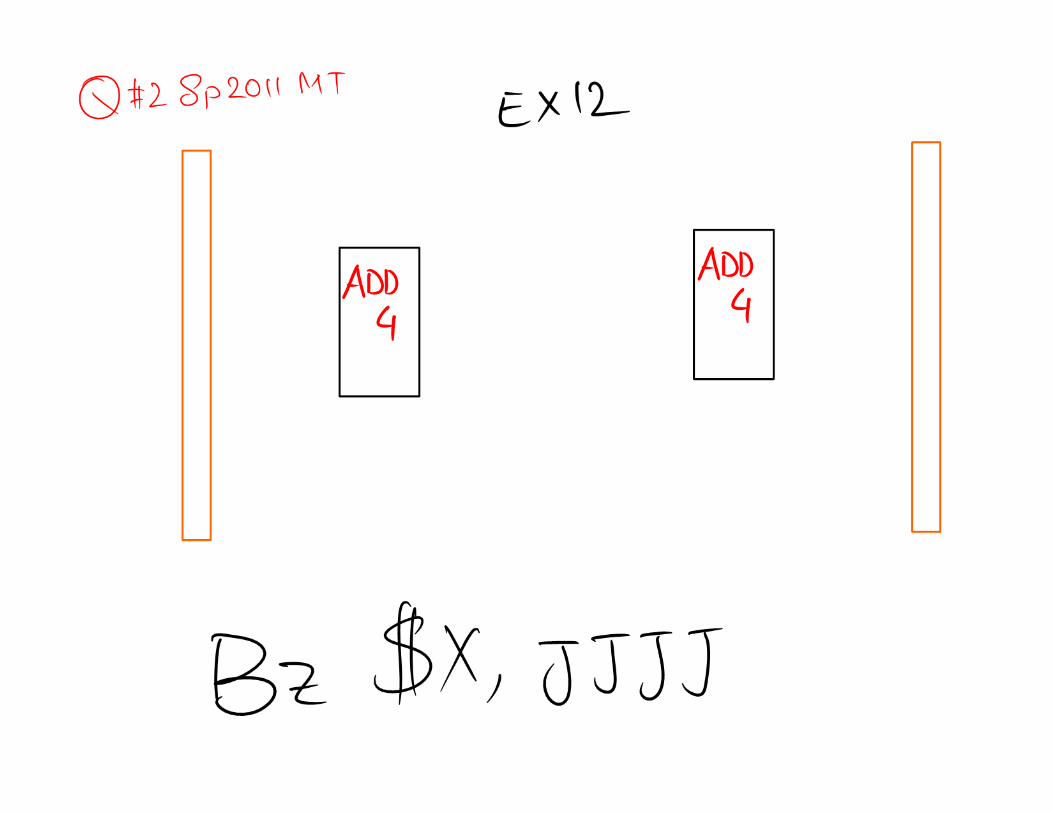
2 ( 20+10+4+4+4+4+4+16+36+6 = 108 points) 70 min.
Pipelining (Modified Lab 7 part 3):
In the Fall 2010 midterm exam, we have an ADD4 unit in each of the two EX stages, EX1 and EX2. Here, those two stages, EX1 and EX2, are merged into EX12. So ADD8 needs an extra clock in EX12 as it has to go through the second ADD4 also.
Further we introduced a BZ (Branch if Zero) instruction. It uses the opcode previously allocated to the SUB3 instruction. The instructions are 32-bits but the addresses are only 16-bit. PC is 16-bit wide and is incremented by a "1". The JJJJ in the BZ $X, JJJJ stands for a 16-bit (4-digit hex) absolute branch address. If the source register $X is a zero then branch to JJJJ takes place [ (PC) <= JJJJ if ($X) = 0 ]. The "D" in "4JJJJ0DS" is a random hex digit and should not be treated as a valid destination, similar to the "DS" in "000000DS" for a NOP instruction. BZ executes from the ID stage.
You need to complete the early branch mechanism (dependency stalls, branch execution by causing PC to be changed to JJJJ and flushing the IF stage instruction, avoiding spurious branch execution during stalling, etc.).
2.1 Complete the design on the page next to next (on page 4).
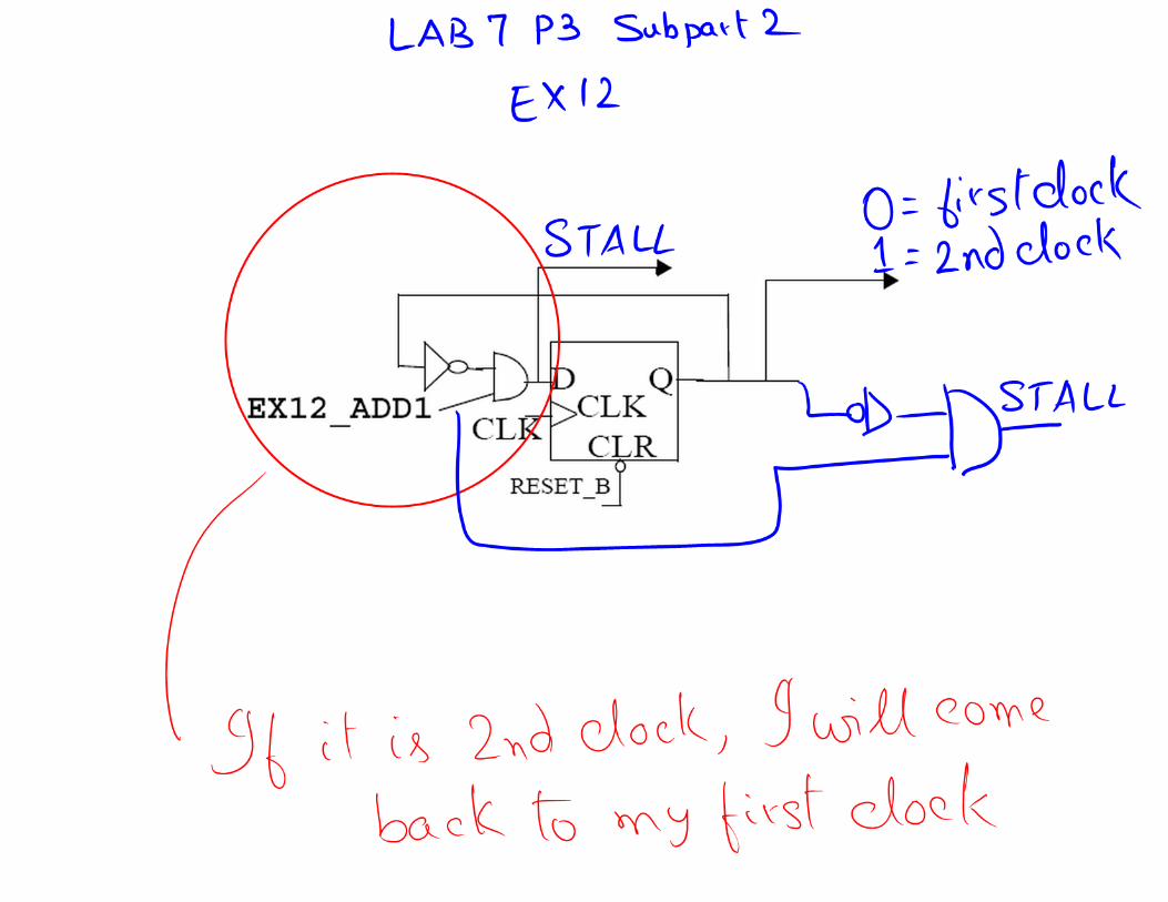
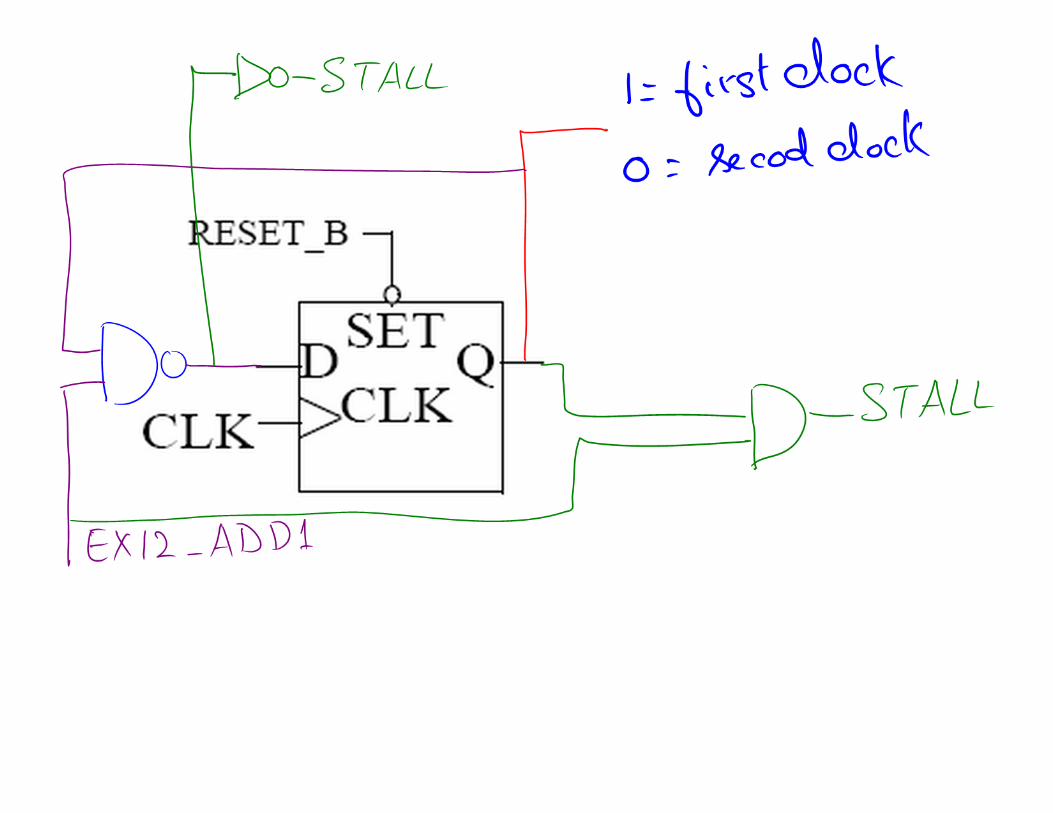
2.2 In you lab 7 Part 3 Subpart 2 (EX1 and EX2 merged case), you used the left side circuit to stall for 1 clock. Complete the design to show the STALL signal. Suppose you are given a flipflop with an asynchronous set as shown in the right side below (instead of the FF with an asynchronous clear as shown on the left). Redesign your stall circuit with this FF and show the STALL signal.
2.3 When STALL_ADD8 is active, you stall the entire pipeline. True / FalseWhen STALL_BR is active, you stall the entire pipeline. True / FalseIF_Flush mechanism here is ___________________ (the same as / different from) the wrist-band mechanism used in our pipelined CPU design.
Instruction Operation Opcode MSD 32-bit instruction in hex
MOV BZ ADD4 ADD8 D=Destination, S=Source
NOP 0 0 0 0 0 000000DS
MOV $R, $X; ($R) <= ($X) 1 0 0 0 8 800000DS
SUB3 $R, $X; ($R) <= ($X) - 3 0 1 0 0 4 400000DS
BZ $X, JJJJ; (PC) <= JJJJ if ($X) = 0 0 1 0 0 2 4JJJJ0DS
ADD4 $R, $X; ($R) <= ($X) + 4 0 0 1 0 2 200000DS
ADD8 $R, $X; ($R) <= ($X) + 8 0 0 0 1 1 100000DS
20pts
10pts
D QCLKCLRCLK
RESET_B
D QCLKSET
CLK
RESET_B
ADD1
4pts

ee457_MT_Sp2011.fm
April 1, 2011 12:09 pm EE457 Midterm Exam - Spring 2011 Page - 3 / 9 C Copyright 2011 Gandhi Puvvada
2.4 In this design we have implemented an early branch. Would a medium branch from EX12 be better?Yes / No / It depends. Explain. ____________________________________________________ _______________________________________________________________________________ _______________________________________________________________________________ _______________________________________________________________________________ _______________________________________________________________________________ _______________________________________________________________________________ Is it possible to postpone executing the BZ instruction all the way into the WB stage (WB!, not EX12)? Not Possible / possible but undesirable / possible and desirable. Explain __________________ _______________________________________________________________________________ _______________________________________________________________________________ _______________________________________________________________________________ _______________________________________________________________________________
2.5 Combining EX1 and EX2 into one EX12 stage (as done here) is ____________________________(always better / always worse / depends on the instruction sequence in the program). Explain. ___ _______________________________________________________________________________ _______________________________________________________________________________ _______________________________________________________________________________ _______________________________________________________________________________
2.6 How come, we carried (PC + 4) to the ID stage in the text book design, but we do not carry (PC+1) to the ID stage here? ______________________________________________________________ _______________________________________________________________________________ _______________________________________________________________________________
2.7 Complete the following "Single Cycle CPU" kind of a design for the pipelined design on the next page. Complete the control unit also.
4pts
4pts
4pts
4pts
16pts
PC
XA
Reg. File
XA
RA
RDR-Write
0
1
0
1A
Cout
A
Cout
XDA+4 A+4
RegWrite
R1_MuxR2_Mux
SKIP1
SKIP2
I-M
EM
PC_EN
RESET_B
ADD4ADD4
ADD4
ADD8
RA
MOV
BZ
+1
0
1
JJJJ
BranchAddress
16
16 1616
PCSource
XD
XD_ZERO
CU
Branch
Single Cycle CPU
complete this

ee457_MT_Sp2011.fm
March 31, 2011 11:00 am EE457 Midterm Exam - Spring 2011 Page - 3 / 9 C Copyright 2011 Gandhi Puvvada
2.4 In this design we have implemented an early branch. Would a medium branch from EX12 be better?Yes / No / It depends. Explain. ____________________________________________________ _______________________________________________________________________________ _______________________________________________________________________________ _______________________________________________________________________________ _______________________________________________________________________________ _______________________________________________________________________________ Is it possible to postpone executing the BZ instruction all the way into the WB stage (WB!, not EX12)? Not Possible / possible but undesirable / possible and desirable. Explain __________________ _______________________________________________________________________________ _______________________________________________________________________________ _______________________________________________________________________________ _______________________________________________________________________________
2.5 Combining EX1 and EX2 into one EX12 stage (as done here) is ____________________________(always better / always worse / depends on the instruction sequence in the program). Explain. ___ _______________________________________________________________________________ _______________________________________________________________________________ _______________________________________________________________________________ _______________________________________________________________________________
2.6 How come, we carried (PC + 4) to the ID stage in the text book design, but we do not carry (PC+1) to the ID stage here? ______________________________________________________________ _______________________________________________________________________________ _______________________________________________________________________________
2.7 Complete the following "Single Cycle CPU" kind of a design for the pipelined design on the next page. Complete the control unit also.
4pts
4pts
4pts
4pts
16pts
PC
XA
Reg. File
XA
RA
RDR-Write
0
1
0
1A
Cout
A
Cout
XDA+4 A+4
RegWrite
R1_MuxR2_Mux
SKIP1
SKIP2
I-M
EM
PC_EN
RESET_B
ADD4ADD4
ADD4
ADD8
RA
MOV
BZ
+1
0
1
JJJJ
BranchAddress
16
16 1616
PCSource
XD
XD_ZERO
CU
Branch
Single Cycle CPU
complete this

ee457_MT_Sp2011.fm
April 1, 2011 12:09 pm
EE457 Midterm
Exam - Spring 2011 Page - 4 / 9
CC
opyright 2011 Gandhi Puvvada
PC
XA
Reg. File
XA
RA
RDR-Write
0
1
0
10
1
A
Cout
A
Cout
Comp Station in ID Stage
ID_XMEX12
P
IF ID EX12 WBComp Station in ID Stage
Q
ID_XA EX12_RA
P=Q
ID_XA Matched with EX12_RA
XD
HDU_BR
EN
XM
EX12
A+4 A+4
FU
EN
RD
Writ
e
RA
XD
RESET_BRESET_BRESET_B
1. Complete all missing connections to
2. Complete the STALL_ADD8 logic in EX12 and STALL_BR logic in ID stage.
4. Draw the logic to produce PCSource, IF_Flush, FORW, SKIP1, SKIP2 on this page itsef.
EX12_ADD4
EX12_ADD8
EX12_RA
WB_RA
WB_Write
WB_RDX1_MuxR1_Mux
R2_Mux
SKIP1
SKIP2
Modified LAB 7 Part 3 Block Diagram
I-M
EMEN
RESET_B
ADD4ADD4STALL_BR
EN
FORW
Q#2
ADD4
AD
D8
RAM
OV
ADD4
AD
D8
RA
MO
V
EX12_MOV
3. Complete all four enable (EN) controls on the pipeline registers (including PC).
ID_ADD4
ID_ADD8
ID_MOV
BZ
XD_ZERO
ID_BZ
+
D QCLKCLRCLK
RESET_B
1
0
1
JJJJ
BranchAddress
16
16 1616
ID_XMEX12
EX12
_Writ
e
PCSource
IF_Flush
STALL_ADD8
EX12_XMEX12

ee457_MT_Sp2011.fm
March 31, 2011 11:00 am
EE457 Midterm
Exam - Spring 2011 Page - 4 / 9
CC
opyright 2011 Gandhi Puvvada
PC
XA
Reg. File
XA
RA
RDR-Write
0
1
0
10
1
A
Cout
A
Cout
Comp Station in ID Stage
ID_XMEX12
P
IF ID EX12 WBComp Station in ID Stage
Q
ID_XA EX12_RA
P=Q
ID_XA Matched with EX12_RA
XD
HDU_BR
EN
XM
EX12
A+4 A+4
FU
EN
RD
Writ
e
RA
XD
RESET_BRESET_BRESET_B
1. Complete all missing connections to
2. Complete the STALL_ADD8 logic in EX12 and STALL_BR logic in ID stage.
4. Draw the logic to produce PCSource, IF_Flush, FORW, SKIP1, SKIP2 on this page itsef.
EX12_ADD4
EX12_ADD8
EX12_RA
WB_RA
WB_Write
WB_RDX1_MuxR1_Mux
R2_Mux
SKIP1
SKIP2
Modified LAB 7 Part 3 Block Diagram
I-M
EMEN
RESET_B
ADD4ADD4STALL_BR
EN
FORW
Q#2
ADD4
AD
D8
RAM
OV
ADD4
AD
D8
RA
MO
V
EX12_MOV
3. Complete all four enable (EN) controls on the pipeline registers (including PC).
ID_ADD4
ID_ADD8
ID_MOV
BZ
XD_ZERO
ID_BZ
+
D QCLKCLRCLK
RESET_B
1
0
1
JJJJ
BranchAddress
16
16 1616
ID_XMEX12
EX12
_Writ
e
PCSource
IF_Flush
STALL_ADD8
EX12_XMEX12

ee457_MT_Sp2011.fm
March 31, 2011 11:00 am EE457 Midterm Exam - Spring 2011 Page - 5 / 9 C Copyright 2011 Gandhi Puvvada
2.8 Now let us try to build a multi-cycle version for the design on the previous page. It is proposed that, we go for a single ALU, which can add a selected constant, (1 for PC and 4 for ADD4 or ADD8).ADD8 uses the ALU twice to add 4 two times. This multi-cycle datapath is similar to the 1st edition design except that here the ALU is built using dynamic logic (like in the 2nd edition). There is an ALUOut register like in the 2nd edition. You need to carefully decide when to take (tap) data from the upstream of the ALUOut register and when to take (tap) data from the downstream of the ALUOut register. We have an IR register (Instruction Register) to hold the instruction at the end of the first state(S0). IR is needed as PC is incremented using the ALU in the very first state. We need to support a NOP instruction here besides MOV, ADD4, ADD8, and BZ.
2.8.1 Complete the datapath and the state diagram for control unit on the next two pages. To some extent, our state diagram resembles the 2nd edition state diagram reproduced below for your reference.We are doing a MOORE kind of state diagram and may be a wasting a few clocks.
36pts

ee457_MT_Sp2011.fm
April 1, 2011 12:09 pm
EE457 Midterm
Exam - Spring 2011 Page - 6 / 9
CC
opyright 2011 Gandhi Puvvada
Multi Cycle CPU
We ________________ (need / do not need) an ALUOut_write control signal.
PC
XA
Reg. File
XA
RA
RDR-Write
B
Cout
XDA+B
RegWrite
I-M
EM
PC_EN
RESET_B
ALU
ADD4
ADD8
RA
MOV
BZ
0
1
JJJJ
BranchAddress
16
321616
PCSource
XD
XD_ZERO
CU
SKIP
IR
PCWritePCWriteCond
0
1
In_Mux0
1
X_Mux
0
1
C_Mux
14
A
16’H0000
ONE/FOUR
IRWrite
ALU
Out
16 32lower 16 of the 32
ASo
urce
[1]
ASo
urce
[0]
PCWrite
ASource[1:0]
PCWriteCond
ONE/FOUR
1
0
R_Mux
SKIP
Concatenate
Strip
CU
PCSource

ee457_MT_Sp2011.fm
March 31, 2011 11:00 am
EE457 Midterm
Exam - Spring 2011 Page - 6 / 9
CC
opyright 2011 Gandhi Puvvada
Multi Cycle CPU
PC
XA
Reg. File
XA
RA
RDR-Write
B
Cout
XDA+B
RegWrite
I-M
EM
PC_EN
RESET_B
ALU
ADD4
ADD8
RA
MOV
BZ
0
1
JJJJ
BranchAddress
16
321616
PCSource
XD
XD_ZERO
CU
SKIP
IR
PCWritePCWriteCond
0
1
In_Mux0
1
X_Mux
0
1
C_Mux
14
A
16’H0000
ONE/FOUR
IRWrite
ALU
Out
16 32lower 16 of the 32
ASo
urce
[1]
ASo
urce
[0]
Branch
PCWrite
ASource[1:0]
PCWriteCond
ONE/FOUR
1
0
R_Mux
SKIP
Concatenate
Strip
We ________________ (need / do not need) an ALUOut_write control signal.

ee457_MT_Sp2011.fm
April 1, 2011 12:09 pm EE457 Midterm Exam - Spring 2011 Page - 7 / 9 C Copyright 2011 Gandhi Puvvada
2.8.2 Mr. Trojan says that, we can easily improve the above state machine by combining states S1, S2, and S6 into one mealy state S126.
Complete the S126 state on the side and also write the new state transition condition from S126 to S0.
BZ
ADD4 or ADD8
ADD4
ADD8
MOV
NOP (= MOV ADD4 ADD8 BZ)S0 S1
S2 S3
S4
S5
S6
No RTLneeded.No signallist.
PCSource=ASource[1:0]=
ONE/FOUR =
RESET_B
S126
To S06pts

ee457_MT_Sp2011.fm
March 31, 2011 11:00 am EE457 Midterm Exam - Spring 2011 Page - 7 / 9 C Copyright 2011 Gandhi Puvvada
2.8.2 Mr. Trojan says that, we can easily improve the above state machine by combining states S1, S2, and S6 into one mealy state S126.
Complete the S126 state on the side and also write the new state transition condition from S126 to S0.
BZ
ADD4 or ADD8
ADD4
ADD8
MOV
NOP (= MOV ADD4 ADD8 BZ)S0 S1
S2 S3
S4
S5
S6
No RTLneeded.No signallist.
PCSource=ASource[1:0]=ONE/FOUR =
RESET_B
S126To S06
pts