pf1550, power management integrated circuit (pmic) for low ... · power management integrated...
TRANSCRIPT

PF1550Power Management Integrated Circuit (PMIC) for low powerapplication processorsRev. 3.0 — 2 May 2018 Data sheet: advance information
1 General description
The PF1550 is a Power Management Integrated Circuit (PMIC) designed specifically foruse with i.MX processors on low-power portable, smart wearable and Internet-of-Things(IoT) applications. It is also capable of providing full power solution to i.MX 7ULP, i.MX6SL, 6UL, 6ULL and 6SX processors.
With three high efficiency buck converter, three linear regulators, RTC supply, andbattery linear charger, the PF1550 can provide power for a complete battery-poweredsystem, including application processors, memory, and system peripherals.
1.1 Features and benefitsThis section summarizes the PF1550 features:
• Input voltage range to PMIC VBUSIN pin via USB bus or AC adapter: 4.1 V to 6.0 V• Buck converters:
– SW1, 1.0 A; 0.6 V to 1.3875 V in 12.5 mV steps, or 1.1 V to 3.3 V in variable steps– SW2, 1.0 A; 0.6 V to 1.3875 V in 12.5 mV steps, or 1.1 V to 3.3 V in variable steps– SW3, 1.0 A; 1.8 V to 3.3 V in 100 mV steps– Soft start– Quiescent current 1.0 μA in ULP mode with light load– Peak efficiency > 90 %– Dynamic voltage scaling on SW1 and SW2– Modes: forced PWM quasi-fixed frequency mode, adaptive variable-frequency mode– Programmable output voltage, current limit and soft start
• LDO regulators– LDO1, 0.75 to 1.5 V/1.8 to 3.3 V, 300 mA with load switch mode– LDO2, 1.8 to 3.3 V, 400 mA– LDO3, 0.75 to 1.5 V/1.8 to 3.3 V, 300 mA with load switch mode– Quiescent current < 1.5 μA in Low-power mode– Programmable output voltage– Soft start and ramp– Current limit protection
• Battery charger– Supports single-cell Lithium Ion/Lithium Polymer batteries– Linear charging (10 mA to 1500 mA input limit)– Up to 6.5 V input operating range– VSYS regulator can withstand transient and DC inputs from 0 V up to +22 V– Programmable charge voltage (3.5 V to 4.44 V)– Programmable charge current (100 mA to 1000 mA)– Programmable charge termination current (5.0 mA to 50 mA)

NXP Semiconductors PF1550Power Management Integrated Circuit (PMIC) for low power application processors
PF1550 All information provided in this document is subject to legal disclaimers. © NXP B.V. 2018. All rights reserved.
Data sheet: advance information Rev. 3.0 — 2 May 20182 / 149
– Integrated 50 mΩ battery isolation MOSFET for operation with no/low battery– Battery supplement mode– Battery discharge overcurrent protection, up to 3.0 A– USB_PHY low dropout linear regulator– Programmable LED driver (status indicator)– JEITA compliant battery temp sensing and charger control– Key charging parameters can be configured and permanently stored in OTP– I2C Control Interface permitting processor control and event detection
• LDO/switch supply– RTC supply VSNVS 3.0 V, 2.0 mA– Battery backed memory including coin cell charger
• DDR memory reference voltage, VREFDDR, 0.5 to 0.9 V, 10 mA• OTP (One time programmable) memory for device configuration
– User programmable start-up sequence, timing, soft-start and power-down sequence– Programmable regulator output voltages and charger parameters
• I2C interface• User programmable Standby, Sleep/Low-power, and Off (REGS_DISABLE) modes• Ambient temperature range −40 °C to 105 °C
1.2 Applications• Smart mobile/wearable devices• Low-power IoT applications• Wireless game controllers• Embedded monitoring systems• Home automation• POS• E-Read

NXP Semiconductors PF1550Power Management Integrated Circuit (PMIC) for low power application processors
PF1550 All information provided in this document is subject to legal disclaimers. © NXP B.V. 2018. All rights reserved.
Data sheet: advance information Rev. 3.0 — 2 May 20183 / 149
2 Application diagram
Low-power application processor
DDR memory
GPS MIPI
VREFDDR
SW2
PF1550
SW1
SW3
LDO1
LDO3
LDO2
VSNVS
Control signals
I2C communication
Li-cell charger
Mini-USB linear charger
USB_PHYMini-USB connector
Coin cell
I2C communication
Parallel control / GPIO
SNVS_IN
Bluetooth
FLASHNAND - NOR
interfaces
Processor real-time SOC/GPU
Processor ARM core
DDR memory Interface
External AMP microphones
speakers
Audio codec
Sensors
aaa-023872
WiFiSD/MMC/
NAND memory
Figure 1. Application diagram

NXP Semiconductors PF1550Power Management Integrated Circuit (PMIC) for low power application processors
PF1550 All information provided in this document is subject to legal disclaimers. © NXP B.V. 2018. All rights reserved.
Data sheet: advance information Rev. 3.0 — 2 May 20184 / 149
2.1 Functional block diagram
Logic and ControlI2C/processor interface/
regulator control/OTP
(flexible configuration)
Linear Li-ion battery charger(22 V surge, power path,
100 mA to 1000 mA charging current)
aaa-023873
PF1550 functional block diagram
LDO1(0.75 V to 3.3 V, 300 mA)
LDO2(1.8 V to 3.3 V, 400 mA)
LDO3(0.75 V to 3.3 V, 300 mA)
BUCK3(1.8 V to 3.3 V, no DVS)
VSNVS (RTC supply)(3.0 V, 2.0 mA)
DDR voltage reference(VINREFDDR/2, 10 mA)
BUCK1(0.6 V to 1.3875 V, 1.0 A, DVS; 1.1 V to 3.3 V, 1.0 A, no DVS)
BUCK2(0.6 V to 1.3875 V, 1.0 A, DVS; 1.1 V to 3.3 V, 1.0 A, no DVS)
Figure 2. Functional block diagram

NXP Semiconductors PF1550Power Management Integrated Circuit (PMIC) for low power application processors
PF1550 All information provided in this document is subject to legal disclaimers. © NXP B.V. 2018. All rights reserved.
Data sheet: advance information Rev. 3.0 — 2 May 20185 / 149
2.2 Internal block diagram
aaa-023874
SW2 DVSand misc reference
SW3and misc reference
SW1IN
SW1LX
EPAD
SW2FB
SW2IN
SW2LX
EPAD
SW3FB
SW3IN
SW3LX
EPAD
VIN
REF
DD
R
VREF
DD
R
LDO
1IN
LDO
1OU
T
LDO
2IN
LDO
2OU
T
LDO
3IN
LDO
3OU
T
THM
VBUSIN
USBPHY
INT2P7
VBATT
LICELLVSNVS
VSYS
VCORE
VDIG
SCL
SDA
VDD
OTP
ON
KEY
RES
ETBM
CU
INTB
PWR
ON
WD
I
CH
GB
VDD
IO
EA anddriver
SW1 DVSand misc reference
EA anddriver
EA anddriver
Watchdogtimer
VREFDDRdivide input by 2
LDO1 LDO2 LDO3
Thermistormonitor
INT2P7LDO
USBPHYLDO
16 MHz clock
32 kHz clock
OTP memory
PF1550 digital coreand state machine
PF1550 analog core(reference and bias current)
VCORELDO
VDIGLDO
coin cellcharger
VSNVS
Digital signal(s)
Analog reference(s)
16 MHz clock / derivative
32 kHz clock / derivative
SW1FB
Figure 3. Internal block diagram
3 Orderable parts
The PF1550 is available only with preprogrammed configurations. These preprogrammeddevices are identified using the program codes from Table 1, which also list theassociated NXP reference designs where applicable. Details of the OTP programming foreach device can be found in Table 83.

NXP Semiconductors PF1550Power Management Integrated Circuit (PMIC) for low power application processors
PF1550 All information provided in this document is subject to legal disclaimers. © NXP B.V. 2018. All rights reserved.
Data sheet: advance information Rev. 3.0 — 2 May 20186 / 149
Table 1. Orderable part variationsPart number[1] Temperature (TA) Package Programming options
MC32PF1550A1EP 1 (Default)
MC32PF1550A2EP 2 (i.MX 7ULP with LPDDR3) [2]
MC32PF1550A3EP 3 (i.MX 6UL with DDR3L)
MC32PF1550A4EP 4 (i.MX 7ULP with LPDDR3)
MC32PF1550A5EP 5 (i.MX 6UL with DDR3)
MC32PF1550A6EP 6 (i.MX 6ULL with DDR3L)
MC32PF1550A7EP
−40 °C to 85 °C (for usein consumer applications)
7 (i.MX 6UL with LPDDR2)
MC34PF1550A1EP 1 (Default)
MC34PF1550A2EP 2 (i.MX 7ULP with LPDDR3) [2]
MC34PF1550A3EP 3 (i.MX 6UL with DDR3L)
MC34PF1550A4EP 4 (i.MX 7ULP with LPDDR3)
MC34PF1550A5EP 5 (i.MX 6UL with DDR3)
MC34PF1550A6EP 6 (i.MX 6ULL with DDR3L)
MC34PF1550A7EP
−40 °C to 105 °C (for usein industrial applications)
98ASA00913D, 40-pin QFN 5.0mm x 5.0 mm with exposed pad
7 (i.MX 6UL with LPDDR2)
[1] For tape and reel, add an R2 suffix to the part number.[2] For internal validation only
4 Pinning information
4.1 Pinning
EPAD(41)
SW1IN
SW1LX
SW2F
B
SW2I
N
SW2L
X
SW3F
B
SW3I
N
SW3L
X
VINREFDDR
VREFDDR
VLDO1IN
VSNVS
VCORE
VDIG
INT2
P7
VBU
SIN
VSYS
VBAT
T
THM
LIC
ELL
CH
GB
USB
PHY
1
2
3
4
5
8
30
29
28
27
26
25
24
6
7
SW1FB
10
9
23
21
22
40 37 36 35 34 33 31323839
11 14 15 16 17 18 20191312
VLDO1
VDDOTP
PWRON
INTB
RESETBMCU
SCL
WDI
STANDBY
ONKEY
VDDIO
SDA
VSYS
VBAT
T
VLD
O3I
N
VLD
O3
VLD
O2
VLD
O2I
N
aaa-023875Transparent top view
PF1550
Figure 4. Pinout diagram
NXP Semiconductors PF1550Power Management Integrated Circuit (PMIC) for low power application processors
PF1550 All information provided in this document is subject to legal disclaimers. © NXP B.V. 2018. All rights reserved.
Data sheet: advance information Rev. 3.0 — 2 May 20187 / 149
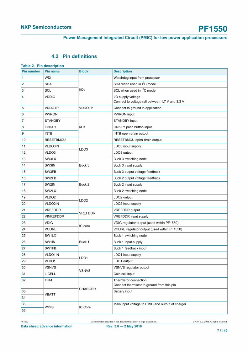
4.2 Pin definitions
Table 2. Pin descriptionPin number Pin name Block Description
1 WDI Watchdog input from processor
2 SDA SDA when used in I2C mode
3 SCL SCL when used in I2C mode
4 VDDIO
I/Os
I/O supply voltageConnect to voltage rail between 1.7 V and 3.3 V
5 VDDOTP VDDOTP Connect to ground in application
6 PWRON PWRON input
7 STANDBY STANDBY input
8 ONKEY ONKEY push button input
9 INTB INTB open-drain output
10 RESETBMCU
I/Os
RESETBMCU open-drain output
11 VLDO3IN LDO3 input supply
12 VLDO3LDO3
LDO3 output
13 SW3LX Buck 3 switching node
14 SW3IN Buck 3 input supply
15 SW3FB
Buck 3
Buck 3 output voltage feedback
16 SW2FB Buck 2 output voltage feedback
17 SW2IN Buck 2 input supply
18 SW2LX
Buck 2
Buck 2 switching node
19 VLDO2 LDO2 output
20 VLDO2INLDO2
LDO2 input supply
21 VREFDDR VREFDDR output
22 VINREFDDRVREFDDR
VREFDDR input supply
23 VDIG VDIG regulator output (used within PF1550)
24 VCOREIC core
VCORE regulator output (used within PF1550)
25 SW1LX Buck 1 switching node
26 SW1IN Buck 1 input supply
27 SW1FB
Buck 1
Buck 1 feedback input
28 VLDO1IN LDO1 input supply
29 VLDO1LDO1
LDO1 output
30 VSNVS VSNVS regulator output
31 LICELLVSNVS
Coin cell input
32 THM Thermistor connectionConnect thermistor to ground from this pin
33
34VBATT
CHARGERBattery input
35
36VSYS IC Core
Main input voltage to PMIC and output of charger

NXP Semiconductors PF1550Power Management Integrated Circuit (PMIC) for low power application processors
PF1550 All information provided in this document is subject to legal disclaimers. © NXP B.V. 2018. All rights reserved.
Data sheet: advance information Rev. 3.0 — 2 May 20188 / 149
Pin number Pin name Block Description
37 VBUSIN Charger input
38 INT2P7 INT2P7 regulator output (used within PF1550 and as thermistor bias)
39 USBPHY USBPHY regulator output
40 CHGB
CHARGER
Charger LED input connectionConnect LED from VSYS to this pin
41 EPAD EPAD Exposed padConnect to ground
5 General product characteristics
5.1 Thermal characteristics
Table 3. Thermal ratingsSymbol Description (Rating) Min. Max. Unit
THERMAL RATINGS
TA Ambient operating temperature range (industrial)Ambient operating temperature range (consumer)
−40−40
10585
°C
TJ Operating junction temperature range [1] −40 125 °C
TST Storage temperature range −65 150 °C
TPPRT Peak package reflow temperature [2] [3] — — °C
QFN40 THERMAL RESISTANCE AND PACKAGE DISSIPATION RATINGS
RΘJA Junction to ambient thermal resistance, natural convectionFour layer board (2s2p)Six layer board (2s4p)Eight layer board (2s6p)
[4] [5] [6] — 2720.617.8
°C/W
RΘJMA Junction to ambient (@200ft/min)Four layer board (2s2p)
[4] [6] — 21.4
°C/W
RΘJB Junction to board [7] — 8.8 °C/W
RΘJCBOTTOM Junction to case bottom [8] — 1.4 °C/W
ΨJT Junction to package top – Natural convection [9] — 0.6 °C/W
[1] Do not operate beyond 125 °C for extended periods of time. Operation above 150 °C may cause permanent damage to the IC. See Thermal ProtectionThresholds for thermal protection features.
[2] Pin soldering temperature limit is for 10 seconds maximum duration. Not designed for immersion soldering. Exceeding these limits may cause amalfunction or permanent damage to the device.
[3] NXP's package reflow capability meets Pb-free requirements for JEDEC standard J-STD-020C. For peak package reflow temperature and moisturesensitivity levels (MSL), go to http://www.nxp.com, search by part number [ remove prefixes/suffixes and enter the core ID to view all orderable parts (forMC33xxxD enter 33xxx), and review parametrics.
[4] Junction temperature is a function of die size, on-chip power dissipation, package thermal resistance, mounting site (board) temperature, ambienttemperature, air flow, power dissipation of other components on the board, and board thermal resistance.
[5] The Board uses the JEDEC specifications for thermal testing (and simulation) JESD51-7 and JESD51-5.[6] Per JEDEC JESD51-6 with the board horizontal.[7] Thermal resistance between the die and the printed circuit board per JEDEC JESD51-8. Board temperature is measured on the top surface of the board
near the package.[8] Thermal resistance between the die and the case top surface as measured by the cold plate method (MIL SPEC-883 Method 1012.1).[9] Thermal characterization parameter indicating the temperature difference between package top and the junction temperature per JEDEC JESD51-2.
When Greek letters are not available, the thermal characterization parameter is written as Psi-JT.

NXP Semiconductors PF1550Power Management Integrated Circuit (PMIC) for low power application processors
PF1550 All information provided in this document is subject to legal disclaimers. © NXP B.V. 2018. All rights reserved.
Data sheet: advance information Rev. 3.0 — 2 May 20189 / 149
5.2 Absolute maximum ratings
Table 4. Maximum ratingsSymbol Description (Rating) Min. Max. Unit
I/Os
VDDIO I/O supply voltage. Connect to voltage rail between 1.7 V and 3.3 V. −0.3 3.6 V
SCL SCL when used in I2C mode. SCLK when used in SPI mode. −0.3 3.6 V
SDA SDA when used in I2C mode. MISO when used in SPI mode. −0.3 3.6 V
RESETBMCU RESETBMCU open drain output −0.3 3.6 V
PWRON PWRON input −0.3 3.6 V
STANDBY STANDBY input −0.3 3.6 V
ONKEY ONKEY push button input −0.3 4.8 V
INTB INTB open-drain output −0.3 3.6 V
WDI Watchdog input from processor −0.3 3.6 V
VDDOTP
VDDOTP Connect to ground in the application −0.3 10 V
BUCK 1
SW1IN Buck 1 input supply −0.3 4.8 V
SW1LX Buck 1 switching node −0.3 4.8 V
SW1FB Buck 1 feedback input −0.3 3.6 V
BUCK 2
SW2IN Buck 2 input supply −0.3 4.8 V
SW2LX Buck 2 switching node −0.3 4.8 V
SW2FB Buck 2 output voltage feedback −0.3 3.6 V
BUCK 3
SW3IN Buck 3 input supply −0.3 4.8 V
SW3LX Buck 3 switching node −0.3 4.8 V
SW3FB Buck 3 output voltage feedback −0.3 3.6 V
LDO1
VLDO1IN LDO1 input supply −0.3 4.8 V
VLDO1 LDO1 output −0.3 3.6 V
LDO2
VLDO2IN LDO2 input supply −0.3 4.8 V
VLDO2 LDO2 output −0.3 3.6 V
LDO3
VLDO3IN LDO3 input supply −0.3 4.8 V
VLDO3 LDO3 output −0.3 3.6 V
VSNVS

NXP Semiconductors PF1550Power Management Integrated Circuit (PMIC) for low power application processors
PF1550 All information provided in this document is subject to legal disclaimers. © NXP B.V. 2018. All rights reserved.
Data sheet: advance information Rev. 3.0 — 2 May 201810 / 149
Symbol Description (Rating) Min. Max. Unit
VSNVS VSNVS regulator output −0.3 3.6 V
LICELL Coin cell input −0.3 3.6 V
CHARGER
VBATT Battery input −0.3 4.8 V
INT2P7 INT2P7 regulator output (used within PF1550 and as thermistor bias) −0.3 3.6 V
THM Thermistor connection. Connect thermistor to ground from this pin. −0.3 3.6 V
VBUSIN Charger input −0.3 24 V
USBPHY USBPHY regulator output −0.3 5.5 V
CHGB Charger LED input connection. Connect LED from VSYS to this pin. −0.3 4.8 V
INPUT/OUTPUT SUPPLY
VINREFDDR VREFDDR input supply −0.3 3.6 V
VREFDDR VREFDDR output −0.3 3.6 V
IC CORE
VSYS Main input voltage to PMIC and output of charger −0.3 4.8 V
VDIG VDIG regulator output (used within PF1550) −0.3 1.65
VCORE VCORE regulator output (used within PF1550) −0.3 1.65 V
ELECTRICAL RATINGS
VESD
ESD ratingsHuman body modelCharge device model (corner pins)Charge device model (all other pins)
[1]
———
±2000±750±500
V
[1] Testing is performed in accordance with the human body model (HBM) (CZAP = 100 pF, RZAP = 1500 Ω), and the charge device model (CDM), Robotic(CZAP = 4.0 pF).

NXP Semiconductors PF1550Power Management Integrated Circuit (PMIC) for low power application processors
PF1550 All information provided in this document is subject to legal disclaimers. © NXP B.V. 2018. All rights reserved.
Data sheet: advance information Rev. 3.0 — 2 May 201811 / 149
5.3 Electrical characteristics
5.3.1 Electrical characteristics – Battery chargerAll parameters are specified at TA = −40 to 105 °C, VBUSIN = 5.0 V, VSYS = 3.7 V,typical external component values, unless otherwise noted. Typical values arecharacterized at VBUSIN = 5.0 V, VSYS = 3.7 V and 25 °C, unless otherwise noted.
Table 5. Global conditionsSymbol Parameter Measurement condition Min. Typ. Max. Unit
CHARGER INPUTS
VBUS VBUSIN voltage range Operating voltage VUVLO — VOVLO V
VBUS_WITHSTAND VBUSIN maximum withstandvoltage rating
— — 22 V
VBUS_OVLO VBUSIN overvoltage threshold Rising 6.0 6.5 7.0 V
VOVLO_HYS VBUSIN overvoltage thresholdhysteresis
Falling 50 150 250 mV
tD-OVLO VBUSIN overvoltage delay 5.0 10 15 µs
VUVLO VBUSIN to GND minimum turnon threshold accuracy
VBUS rising 3.8 4.0 4.2 V
VUVLO-HYS VBUSIN UVLO hysteresis 400 500 600 mV
VIN2SYS_50 VBUSIN to VSYS minimum turnon threshold accuracy
VBUS_LIN rising, 50 mV setting 20 50 80 mV
VIN2SYS_175 VBUSIN to VSYS minimum turnon threshold accuracy
VBUS_LIN rising, 175 mVsetting
100 175 250 mV
VBUS_LIN_DPM_REG VBUSIN adaptive voltageregulation threshold
4.4 V setting (default) 4.3 4.4 4.5 V
VDPM_REG VBUSIN adaptive voltageregulation threshold accuracy
Programmable at 3.9 V to 4.6 V −100 — 100 mV
Table 6. Input currentsSymbol Parameter Measurement condition Min. Typ. Max. Unit
VBUSIN INPUT CURRENT LIMIT
ILIM10 Charger input current limit (10mA settings)
10 mA 6.0 8.5 11 mA
ILIM15 Charger input current limit (15mA settings)
15 mA 10.5 12.75 16 mA
ILIM20 Charger input current limit (20mA settings)
20 mA 14 17 21 mA
ILIM25 Charger input current limit (25mA settings)
25 mA 17.5 21.25 26 mA
ILIM30 Charger Input Current Limit(30mA setting)
30 mA 21 25.5 30 mA
ILIM35 Charger input current limit (35mA settings)
35 mA 24.5 29.75 35 mA
ILIM40 Charger input current limit(40mA settings)
40 mA 28 34 40 mA
ILIM45 Charger input current limit (45mA settings)
45 mA 31.5 38.25 45 mA
ILIM50 Charger input current limit (50mA settings)
50 mA 35 42.5 50 mA

NXP Semiconductors PF1550Power Management Integrated Circuit (PMIC) for low power application processors
PF1550 All information provided in this document is subject to legal disclaimers. © NXP B.V. 2018. All rights reserved.
Data sheet: advance information Rev. 3.0 — 2 May 201812 / 149
Symbol Parameter Measurement condition Min. Typ. Max. Unit
ILIM100 Charger input current limit (100mA settings)
100 mA 85 95 105 mA
ILIM150 Charger input current limit (150mA settings)
150 mA 125 137.5 160 mA
ILIM200 Charger input current limit (200mA settings)
200 mA 170 190 210 mA
ILIM300 Charger input current limit (300mA setting)
300 mA 260 285 320 mA
ILIM400 Charger input current limit (400mA settings)
400 mA 345 380 425 mA
ILIM500 Charger input current limit (500mA settings)
500 mA 430 475 530 mA
ILIM600 Charger input current limit (600mA settings)
600 mA 520 570 640 mA
ILIM700 Charger input current limit (700mA settings)
700 mA 610 665 750 mA
ILIM800 Charger input current limit (800mA settings)
800 mA 690 760 850 mA
ILIM900 Charger input current limit (900mA settings)
900 mA 780 855 950 mA
ILIM1000 Charger input current limit(1000 mA settings)
1000 mA 855 950 1100 mA
ILIM1500 Charger input current limit(1500 mA settings)
1500 mA 1260 1400 1700 mA
RINSD Input self discharge resistance 18 30 42 kΩ
IBATTLEAK Leakage current Leakage current from VBATTto VBUSIN. VBATT = 4.2 V,BATFET closed, VBUSIN = 0 V.Current measured into VBATTpin at 25 °C
0 — 5.0 µA
IQ_CHARGER Charger quiescent current(BATFET enabled, normalmode)
25 °C only; charger in CC state;ICC = 100 mA
0 2.5 5.0 mA
IQ_CHARGER_LQM Charger quiescent current (lowpower mode, charging enabled,10 to 50 mA input current limitsetting, VBATT > 2.8 V andLED driver OFF)
25 °C only; charger in CC state 0 1.5 3.0 mA
TSSVBUS_LIN Soft start time (VBUSIN = 5.0V, time between input LDOenabled and VSYS going to 90% of regulation
No input current limitationevent, measured in Normalmode
— — 30 ms
Table 7. Internal 2.7 V Regulator (INT2P7)Symbol Parameter Measurement condition Min. Typ. Max. Unit
VGDRV Output voltage 2.6 2.7 2.8 V
IGDRV Output current 5.0 — — mA
VDO(GDRV) Dropout voltage 0 — 800 mV
Table 8. Switch impedances and leakage currentsSymbol Parameter Measurement Condition Min. Typ. Max. Unit
RVBUS_LIN2SYS VBUSIN to VSYS resistance 100 250 550 mΩ
RBATFET_QFN VBATT to VSYS resistance 50 75 120 mΩ

NXP Semiconductors PF1550Power Management Integrated Circuit (PMIC) for low power application processors
PF1550 All information provided in this document is subject to legal disclaimers. © NXP B.V. 2018. All rights reserved.
Data sheet: advance information Rev. 3.0 — 2 May 201813 / 149
Symbol Parameter Measurement Condition Min. Typ. Max. Unit
ISYS VSYS leakage current VSYS = 0 V, VBATT = 4.2 V,SHIP mode
0 0.2 10 µA
IBATT_OC VBATT reverse ILIM quiescentcurrent when VBUSIN = 0 V
VBUSIN = 0 V, VSYS = VBATT= 4.2 V, BATFET enabled,battery overcurrent enabled
— — 100 µA
Table 9. Linear transientsSymbol Parameter Measurement condition Min. Typ. Max. Unit
VPK-PK Load transient peak-to-peak VBUSIN = 5.0 V, VBATT = 3.6V, ICHG = 500 mA, VSYS loadstep 1.0 A/µs
10 400 850 mV
VOV_SHT Load transient overshoot VBUSIN = 5.0 V, VBATT = 3.6V, ICHG = 500 mA, VSYS loadstep 1.0 A/µs
0 200 500 mV
VUND_SHT Load transient undershoot VBUSIN = 5.0 V, VBATT = 3.6V, ICHG = 500 mA, VSYS loadstep 1.0 A/µs
0 200 500 mV
Table 10. Charger characteristicsSymbol Parameter Measurement condition Min. Typ. Max. Unit
VCHGCV_RANGE CHGCV output voltage range See register map for constantvoltage programmable range
3.5 — 4.44 V
CVACC CHGCV output accuracy innormal charging
— — ±1 %
VSYSMIN0 VSYS output voltage (3.5 Voption)
VSYSMIN = 0x00 (3.5 V option) 3.395 3.5 3.605 V
VSYSMIN1 VSYS output voltage (3.7 Voption)
VSYSMIN = 0x01 (3.7 V option) 3.589 3.7 3.811 V
VSYSMIN2 VSYS output voltage (4.3 Voption)
VSYSMIN = 0x02 (4.3 V option) 4.171 4.3 4.429 V
VSYSMINLOOP0 VSYSMIN loop threshold (3.5 Voption)
3.0 3.2 3.39 V
VSYSMINLOOP1 VSYSMIN loop threshold (3.7 Voption)
3.2 3.4 3.585 V
VSYSMINLOOP2 VSYSMIN loop threshold (4.3 Voption)
3.83 4.0 4.17 V
IFC Output current range Constant current programmablerange CHG_CC[4:0]
100 — 1000 mA
IFCACC1 Output current accuracy −10 — 10 %
IEOC Charger IEOC range 5.0 — 50 mA
tDB(IEOC) Debounce time for chargetermination
20 32 44 ms
IEOC_ACC_5mA Charger IEOC accuracy (5.0 mAsettings)
IEOC = 5 mA 1.0 5.0 12 mA
IEOC_ACC_10mA Charger IEOC accuracy (10 mAsettings)
IEOC = 10 mA 4.0 10 16 mA
IEOC_ACC_50mA Charger IEOC accuracy (50 mAsetting)
IEOC = 50 mA 40 50 60 mA
VPRECHG Precharge threshold VBATT rising 2.7 2.8 2.9 V
VPRECHG_HYS Precharge threshold hysteresis 50 100 150 mV
IPRECHG Precharge current 30 45 60 mA

NXP Semiconductors PF1550Power Management Integrated Circuit (PMIC) for low power application processors
PF1550 All information provided in this document is subject to legal disclaimers. © NXP B.V. 2018. All rights reserved.
Data sheet: advance information Rev. 3.0 — 2 May 201814 / 149
Symbol Parameter Measurement condition Min. Typ. Max. Unit
IPRECHG.LPM Charging current in LPM and 2.8V < VBATT < 3.1 V
0.75 1.0 1.25 mA
VRESTART Charger restart threshold (100mV settings)
VBATT below CHGCV[5:0] 50 100 150 mV
VRESTART Charger restart threshold (150mV setting)
VBATT below CHGCV[5:0] 100 150 200 mV
VRESTART Charger restart threshold (200mV settings)
VBATT below CHGCV[5:0] 150 200 250 mV
tDB(VRCH) Debounce time on VRESTART 20 32 44 ms
VBATOV BATTOVP range CHGCV x1.025
CHGCV x 1.05 CHGCV x1.075
V
VBATOV_HYS BATTOVP hysteresis VBATT falling from BATTOVP CHGCV x0.015
CHGCV x0.025
CHGCV x0.035
V
Table 11. Power-path managementSymbol Parameter Measurement condition Min. Typ. Max. Unit
VSPLM Supplement mode voltagethreshold
Entering supplement modewhen VSYS < VBATT
10 40 75 mV
Table 12. Watchdog timerSymbol Parameter Measurement condition Min. Typ. Max. Unit
tWD Watchdog timer period — 80 — s
tWDACC Watchdog timer accuracy −20 0 20 %
Table 13. Charger timerSymbol Parameter Measurement condition Min. Typ. Max. Unit
tPRECHG Precharge time (fixed 45 mA) Applies to low batteryprequalification mode, 500 mAsettings
— 30 — min
tFC Fast charge constant currentand constant voltage time
Adjustable from 2 to 14 in 2 hoursteps
— 4.0 — hrs
tEOC End-of-charge time Adjustable from 0 to 70 in 10min steps
— 30 — min
tacc Timer accuracy All timers associated with thecharger block
−20 — 20 %
tSCIDG Charger state change interruptdelay
0 1.0 2.0 ms
tINLIM VBUS_VOK delay from VDIGready following VBUSINinsertion (see charger startupdiagram)
0 100 200 µs
Table 14. Battery overcurrent protectionSymbol Parameter Measurement condition Min. Typ. Max. Unit
tBOVCR Battery overcurrent debouncetime
Response time to BATFET open(OTP option)
12.8 16 19.2 ms
tBOVCRI Battery overcurrent interruptdebounce time
Response time to generateinterrupt
2.4 3.0 3.6 ms

NXP Semiconductors PF1550Power Management Integrated Circuit (PMIC) for low power application processors
PF1550 All information provided in this document is subject to legal disclaimers. © NXP B.V. 2018. All rights reserved.
Data sheet: advance information Rev. 3.0 — 2 May 201815 / 149
Symbol Parameter Measurement condition Min. Typ. Max. Unit
IBOVCR Battery overcurrent thresholdrange
Programmable from 2.0 A to 4.0A in three steps
2.0 — 4.0 A
IBOVCRACC_2A Battery overcurrent thresholdaccuracy (2.2 A setting)
1.0 2.2 3.2 A
IBOVCRACC_3A Battery overcurrent thresholdaccuracy (2.8 A setting)
1.6 2.8 4 A
IBOVCRACC_4A Battery overcurrent thresholdaccuracy (3.2 A setting)
2.0 3.2 4.6 A
RSYSDISCH SYS self-discharge resistor inSHIP mode
480 600 720 Ω
Table 15. Thermal regulationSymbol Parameter Measurement condition Min. Typ. Max. Unit
TREG Thermal regulation threshold (80°C setting)
Temperature at which chargecurrent begins to decrease
— 80 — °C
TREG Thermal regulation threshold (95°C Setting)
Temperature at which chargecurrent begins to decrease
— 95 — °C
TREG Thermal regulation threshold(110 °C setting)
Temperature at which chargecurrent begins to decrease
— 110 — °C
Table 16. Battery thermistor monitorSymbol Parameter Measurement Condition Min. Typ. Max. Unit
VNTECREF NTECREF voltage 2.6 2.7 2.8 V
VTN10C Thermistor threshold (−10 °Csettings)
−10 °C 0.79*VNTECREF 0.82*VNTECREF 0.85*VNTECREF V
VT0C Thermistor threshold (0 °Csettings)
0 °C 0.71*VNTECREF 0.74*VNTECREF 0.77*VNTECREF V
VT10C Thermistor threshold (10 °Csettings)
10 °C 0.62*VNTECREF 0.65*VNTECREF 0.68*VNTECREF V
VT45C Thermistor threshold (45 °Csettings)
45 °C 0.31*VNTECREF 0.33*VNTECREF 0.35*VNTECREF V
VT55C Thermistor threshold (55 °Csettings)
55 °C 0.25*VNTECREF 0.26*VNTECREF 0.27*VNTECREF V
VT60C Thermistor threshold (60 °Csettings)
60 °C 0.22*VNTECREF 0.23*VNTECREF 0.24*VNTECREF V
VT_HYS Battery temperature hysteresis All settings 0.5 2.5 5.0 °C
Table 17. USBPHY LDOSymbol Parameter Measurement condition Min. Typ. Max. Unit
VUSB_PHY Output voltage IOUT = 10 mA; 3.3 V and 4.9 Vsettings. VBUSIN = 5.5 V
−5.0 — 5.0 %
IUSB_PHY Maximum output current 60 — — mA
USBRDIS Internal discharge resistance 500 1000 1500 Ω
USBCAPSTA Output capacitor for stableoperation
0 µA < IOUT < 60 mA, MAX ESR= 10 mΩ
0.7 1.0 2.2 µF
IQUSB Quiescent supply current — 35 — µA
USBPHYLDREG DC load regulation VBUSIN = 5.5 V, 30 µA < IOUT <60 mA
0 5.0 13 mV
USBPHYDO Dropout voltage VBUSIN = 5.0 V, IOUT = 60 mA — 200 350 mV

NXP Semiconductors PF1550Power Management Integrated Circuit (PMIC) for low power application processors
PF1550 All information provided in this document is subject to legal disclaimers. © NXP B.V. 2018. All rights reserved.
Data sheet: advance information Rev. 3.0 — 2 May 201816 / 149
Symbol Parameter Measurement condition Min. Typ. Max. Unit
USBPHYILIM Output current limit 65 150 200 mA
PSRRUSB_PHY PSRR VBUSIN = 5.5 V, COUT = 1.0 µF 55 60 75 dB
Table 18. LED characteristicsSymbol Parameter Measurement condition Min. Typ. Max. Unit
VLED LED input voltage operatingrange (anode to ground)
3.5 — VSYS V
VCHGB_IN CHGB input voltage operatingrange, LED driver enabled
1.0 — 3.0 V
ILED LED current accuracy 4.0 6.0 8 mA
TON LED duty cycle range Programmable from 10 % to 100% duty cycle in 10 % steps
10 — 100 %
TLEDRUP LED ramp up Settings depend on duty cycle 50 — 500 ms
TLEDRDN LED ramp down Settings depend on duty cycle 50 — 500 ms
FLED LED frequency Programmable from 0.5 Hz to256 Hz
0.5 — 256 Hz
5.3.2 Electrical characteristics – SW1 and SW2All parameters are specified at TA = −40 to 105 °C, VSYS = VSWxIN = 2.5 to 4.5 V, VSWx= 1.2 V, ISWx = 200 mA, typical external component values, fSWx = 2.0 MHz, unlessotherwise noted. Typical values are characterized at VSYS = VSWxIN = 3.6 V, VSWx =1.1 V, ISWx = 100 mA, and 25 °C, unless otherwise noted.
Table 19. SW1 and SW2 electrical characteristicsSymbol Parameter Min. Typ. Max. Unit
VSWxIN Operating input voltage 2.5 — 4.5 V
ISWx Rated output current 1000 — — mA
VSWx Output voltage accuracyDVS enabled mode (OTP_SWx_DVS_SEL = 0)Normal power mode, 2.5 V < VSWxIN < 4.5 V, 0 < ISWx < 1.0 A0.6 V ≤ VSWx ≤ 1.0 V
−15 — 15 mV
VSWx Output voltage accuracyDVS enabled mode (OTP_SWx_DVS_SEL = 0)Normal power mode, 2.5 V < VSWxIN < 4.5 V, 0 < ISWx < 1.0 A1.0 V < VSWx ≤ 1.3875 V
−2.0 — 2.0 %
VSWx Output voltage accuracyDVS enabled mode (OTP_SWx_DVS_SEL = 0)Low-power mode, 2.5 V < VSWxIN < 4.5 V, 0 < ISWx < 0.1 A0.6 V ≤ VSWx ≤ 1.0 V
−30 — 30 mV
VSWx Output voltage accuracyDVS enabled mode (OTP_SWx_DVS_SEL = 0)Low-power mode, 2.5 V < VSWxIN < 4.5 V, 0 < ISWx < 0.1 A1.0 V < VSWx ≤ 1.3875 V
−3.0 — 3.0 %
VSWx Output voltage accuracyDVS disabled mode (OTP_SWx_DVS_SEL = 1)Normal power mode, 2.5 V < VSWxIN < 4.5 V, 0 < ISWx < 1.0 A1.1 V ≤ VSWx ≤ 1.5 V
−45 — 45 mV
VSWx Output voltage accuracyDVS disabled mode (OTP_SWx_DVS_SEL = 1)Normal power mode, 2.5 V < VSWxIN < 4.5 V, 0 < ISWx < 1.0 A1.8 V ≤ VSWx ≤ 3.3 V
−3.0 — 3.0 %

NXP Semiconductors PF1550Power Management Integrated Circuit (PMIC) for low power application processors
PF1550 All information provided in this document is subject to legal disclaimers. © NXP B.V. 2018. All rights reserved.
Data sheet: advance information Rev. 3.0 — 2 May 201817 / 149
Symbol Parameter Min. Typ. Max. Unit
VSWx Output voltage accuracyDVS disabled mode (OTP_SWx_DVS_SEL = 1)Low-power mode, 2.5 V < VSWxIN < 4.5 V, 0 < ISWx < 0.1 A1.1 V < VSWx ≤ 1.5 V
−55 — 55 mV
VSWx Output voltage accuracyDVS disabled mode (OTP_SWx_DVS_SEL = 1)Low-power mode, 2.5 V < VSWxIN < 4.5 V, 0 < ISWx < 0.1 A1.8 V ≤ VSWx ≤ 3.3 V
−4.0 — 4.0 %
ΔVSWx Output ripple — 5.0 — mV
SWxEFF EfficiencyVSWxIN = 3.6 V, LSWx = 1.0 µH, DCR = 50 mΩLP/ ULP mode, 1.2 V, 1.0 mA
— 88 — %
SWxEFF EfficiencyVSWxIN = 3.6 V, LSWx = 1.0 µH, DCR = 50 mΩNormal power mode, 1.2 V, 50 mA
— 90 — %
SWxEFF EfficiencyVSWxIN = 3.6 V, LSWx = 1.0 µH, DCR = 50 mΩNormal power mode, 1.2 V, 150 mA
— 92 — %
SWxEFF EfficiencyVSWxIN = 3.6 V, LSWx = 1.0 µH, DCR = 50 mΩNormal power mode, 1.2 V, 400 mA
— 89 — %
SWxEFF EfficiencyVSWxIN = 3.6 V, LSWx = 1.0 µH, DCR = 50 mΩNormal power mode, 1.2 V, 1000 mA
— 83 — %
ISWxLIMH Current limiter peak (high-side MOSFET) current detectionSWxILIM[1:0] = 00SWxILIM[1:0] = 01SWxILIM[1:0] = 10SWxILIM[1:0] = 11
0.70.81.01.4
1.01.21.52.0
1.31.62.02.6
A
ISWxLIML Current limiter low-side MOSFET current detection (sinking current) 0.7 1.0 1.3 A
ISWxQ Quiescent current (at 25 °C)Low-power mode with DVS disabled (OTP_SWx_DVS_SEL = 1)
—
1.0
—
µA
ISWxQ Quiescent current (at 25 °C)Low-power mode with DVS enabled (OTP_SWx_DVS_SEL = 0)
—
6.0
—
µA
ISWxQ Quiescent current (at 25 °C)Normal power mode with DVS disabled (OTP_SWx_DVS_SEL = 1)
—
5.5
—
µA
ISWxQ Quiescent current (at 25 °C)Normal power mode with DVS enabled (OTP_SWx_DVS_SEL = 0)
—
10
—
µA
VSWxOSH Startup overshoot (Normal mode)ISWx = 0 mADVS speed = 12.5 mV/4 µs, VSYS = VSWxIN = 3.6 V, VSWx = 1.35 V
— — 25 mV
tONSWx Turn on time10 % to 90 % of end valueDVS speed = 12.5 mV/4 µs, VSYS = VSWxIN = 3.6 V, VSWx = 1.35 V
— — 500 µs
VSWxLOTR Transient load regulation (Normal power mode)Transient load = 50 mA to 250 mA, di/dt = 200 mA/μs
OvershootUndershoot
——
2525
——
mV
RONSWxP SWx P-MOSFET RDS(on) at VSWxIN = 3.6 V — 200 — mΩ
RONSWxN SWx N-MOSFET RDS(on) at VSWxIN = 3.6 V — 150 — mΩ
RSWxDIS Turn off discharge resistance — 500 — Ω

NXP Semiconductors PF1550Power Management Integrated Circuit (PMIC) for low power application processors
PF1550 All information provided in this document is subject to legal disclaimers. © NXP B.V. 2018. All rights reserved.
Data sheet: advance information Rev. 3.0 — 2 May 201818 / 149
5.3.3 Electrical characteristics – SW3All parameters are specified at TA = −40 to 105 °C, VSYS = VSW3IN = 2.5 to 4.5 V, VSW3= 1.8 V, ISW3 = 200 mA, typical external component values, fSW3 = 2.0 MHz, unlessotherwise noted. Typical values are characterized at VSYS = VSW3IN = 3.6 V, VSW3 =1.8 V, ISW3 = 200 mA, and 25 °C, unless otherwise noted.
Table 20. SW3 electrical characteristicsSymbol Parameter Min. Typ. Max. Unit
VSW3IN Operating input voltage 2.5 — 4.5 V
VSW3 Output voltage accuracy (all voltage settings)Normal power mode, 2.5 V < VSW3IN < 4.5 V, 0 < ISW3 < 1.0 A
−2.0
—
2.0
%
VSW3 Output voltage accuracy (all voltage settings)Low-power mode, 2.5 V < VSW3IN < 4.5 V, 0 < ISW3 < 0.1 A
−3.0
—
3.0
%
ΔVSW3 Output ripple — 5.0 — mV
SW3EFF
EfficiencyVSW3IN = 3.6 V, LSW3 = 1.0 µH, DCR = 50 mΩLP/ ULP Mode, 1.8 V, 1.0 mA
—
88
—
%
SW3EFF
EfficiencyVSW3IN = 3.6 V, LSWx = 1.0 µH, DCR = 50 mΩNormal power mode, 1.8 V, 50 mA
—
90
—
%
SW3EFF
EfficiencyVSW3IN = 3.6 V, LSWx = 1.0 mH, DCR = 50 mΩNormal power mode, 1.8 V, 100 mA
—
91
—
%
SW3EFF
EfficiencyVSW3IN = 3.6 V, LSWx = 1.0 µH, DCR = 50 mΩNormal power mode, 1.8 V, 400 mA
—
92
—
%
SW3EFF
EfficiencyVSW3IN = 3.6 V, LSWx = 1.0 µH, DCR = 50 mΩNormal power mode, 1.8 V, 1000 mA
—
83
—
%
ISW3LIMH Current limiter peak (high-side MOSFET) current detectionSW3ILIM[1:0] = 00SW3ILIM[1:0] = 01SW3ILIM[1:0] = 10SW3ILIM[1:0] = 11
0.70.81.01.4
1.01.21.52.0
1.31.62.02.6
A
ISW3LIML Current limiter low-side MOSFET current detection (sinking current) 0.7 1.0 1.3 A
ISW3Q Quiescent current (at 25 °C)Low-power mode
—
1.0
—
µA
VSW3OSH Start-up overshoot (Normal mode)ISW3 = 0 mAVSYS = VSW3IN = 3.6 V, VSW3 = 1.8 V
— — 50 mV
tONSW3 Turn on time10 % to 90 % of end valueVSYS = VSW3IN = 3.6 V, VSW3 = 1.8 V
— — 500 µs
VSW3LOTR Transient load regulation (Normal power mode)Transient load = 50 mA to 250 mA, di/dt = 200 mA/μs
OvershootUndershoot
——
5050
——
mV
RONSW3N SW3 N-MOSFET RDS(on) at VSW3IN = 3.6 V — 150 — mΩ
RONSW3P SW3 P-MOSFET RDS(on) at VSW3IN = 3.6 V — 200 — mΩ
RSW3DIS Turn off discharge resistance — 300 — Ω

NXP Semiconductors PF1550Power Management Integrated Circuit (PMIC) for low power application processors
PF1550 All information provided in this document is subject to legal disclaimers. © NXP B.V. 2018. All rights reserved.
Data sheet: advance information Rev. 3.0 — 2 May 201819 / 149
5.3.4 Electrical characteristics – LDO1All parameters are specified at TA = −40 to 105 °C, VSYS = 2.5 to 4.5 V, VLDOIN1 =3.6 V, VLDO1[4:0] = 11111, ILDO1 = 10 mA, typical external component values, unlessotherwise noted. Typical values are characterized at VSYS = 3.6 V, VLDOIN1 = 3.6 V,VLDO1[4:0] = 11111, ILDO1 = 10 mA, and 25 °C, unless otherwise noted.
Table 21. LDO1 electrical characteristicsSymbol Parameter Min. Typ. Max. Unit
VLDO1IN Operating input voltageVLDO1 + 250 mV ≤ VSYS ≤ 4.5 V
1.0
—
4.5
V
VLDO1NOM Nominal output voltage — See Table 41 — V
ILDO1MAX Rated output load current, Normal mode 300 — — mA
ILDO1MAXLPM Rated output load current, Low-power mode 10 — — mA
VLDO1TOL Output voltage tolerance, Normal modeVLDO1INMIN < VLDO1IN < 4.5 V, 0 mA < ILDO1 ≤ 300 mA0.8 V ≤ VLDO1 < 1.8 V1.8 V ≤ VLDO1 ≤ 3.3 VVLDO1INMIN < VLDO1IN < 4.5 V, 0 mA < ILDO1 < 10 mA (Low-powermode)
−2.5−2.5−4.0
———
2.52.54.0
%
ILDO1LIM Current limitILDO1 when VLDO1 is forced to VLDO1NOM/2
320 — 1000 mA
ILDO1OCP LDO1FAULTI threshold (also used to disable LDO1 whenREGSCPEN = 1)
320 — 1000 mA
ILDO1Q Quiescent current (at 25 °C)No load, change in IVSYS and IVLDOIN1When LDO1 enabled in Normal modeWhen LDO1 enabled in Low-power mode
——
172.5
——
µA
RDSON_QFN_LDO1 Dropout on resistance — — 350 mΩ
PSRRLDO1 PSRRILDO1 = 150 mA, 20 Hz to 20 kHzVLDO1 = 3.30 V, VLDO1IN = 3.8 V, VSYS = 4.2 V
—
56
—
dB
TRVLDO1 Turn on time10 % to 90 % of end valueVLDO1INMIN < VLDO1IN ≤ 4.5 V, ILDO1 = 0.0 mA
—
200
500
µs
RLDO1DIS Turn off discharge resistance — 250 — Ω
LDO1OUTOSHT Start-up overshoot (% of final value)VLDO1INMIN < VLDO1IN ≤ 4.5 V, ILDO1 = 0.0 mA
—
1.0
2.0
%
VLDO1LOTR Transient load responseVLDO1INMIN < VLDO1IN ≤ 4.5 V, ILDO1 = 10 mA to 200 mA in 10 μs
OvershootUndershoot
——
5050
——
mV
5.3.5 Electrical characteristics – LDO2All parameters are specified at TA = −40 to 105 °C, VSYS = 3.6 V, VLDOIN2 = 3.6 V,VLDO2[3:0] = 1111, ILDO2 = 10 mA, typical external component values, unless otherwisenoted. Typical values are characterized at VSYS = 3.6 V, VLDOIN2 = 3.6 V, VLDO2[3:0] =1111, ILDO2 = 10 mA, and 25 °C, unless otherwise noted.

NXP Semiconductors PF1550Power Management Integrated Circuit (PMIC) for low power application processors
PF1550 All information provided in this document is subject to legal disclaimers. © NXP B.V. 2018. All rights reserved.
Data sheet: advance information Rev. 3.0 — 2 May 201820 / 149
Table 22. LDO2 electrical characteristicsSymbol Parameter Min. Typ. Max. Unit
VLDO2IN Operating input voltage1.8 V ≤ VLDO2NOM ≤ 2.5 V2.6 V ≤ VLDO2NOM ≤ 3.3 V
2.8VLDO2NOM + 0.250
––
4.54.5
V
VLDO2NOM Nominal output voltage — See Table 43 — V
ILDO2MAX Rated output load current, Normal mode 400 — — mA
ILDO2MAXLPM Rated output load current, Low-power mode 10 — — mA
VLDO2TOL Output voltage toleranceVLDO2INMIN < VLDO2IN < 4.5 V10.0 mA ≤ ILDO2 < 400 mA0.0 mA < ILDO2 < 10 mA (Low-power mode)
−2.0−4.0
——
2.04.0
%
ILDO2LIM Current limitILDO2 when VLDO2 is forced to VLDO2NOM/2
450 750 1050 mA
ILDO2OCP LDO2FAULTI threshold (also used to disable LDO2when REGSCPEN = 1)
450 — 1050 mA
ILDO2Q Quiescent Current (25 °C)No load, change in IVSYS and IVLDO2INWhen VLDO2 enabled in Normal modeWhen VLDO2 enabled in Low-power mode
——
151.5
——
µA
RDSON_QFN_LDO2 Dropout on resistance — — 300 mΩ
PSRRVLDO2 PSRRILDO2 = 200 mA, 20 Hz to 20 kHzVLDO2 = 3.30 V, VLDO2IN = 3.9 V, VSYS = 4.2 V
—
60
—
dB
tONLDO2 Turn on time10 % to 90 % of end valueVLDO2INMIN < VLDO2IN ≤ 4.5 V, ILDO2 = 0.0 mA
— 200 500 µs
RLDO2DIS Turn off discharge resistance — 250 — Ω
LDO2OUTOSHT Start-up overshoot (% of final value)VLDO2INMIN < VLDO2IN ≤ 4.5 V, ILDO2 = 0.0 mA
— 1.0 2.0 %
VLDO2LOTR Transient load responseVLDO2INMIN < VLDO2IN ≤ 4.5 V, ILDO2 = 10 mA to 100 mA in10 μs
OvershootUndershoot
——
5050
——
mV
5.3.6 Electrical characteristics – LDO3All parameters are specified at TA = −40 to 105 °C, VSYS = 2.5 to 4.5 V, VLDOIN3 =3.6 V, VLDO3[4:0] = 11111, ILDO3 = 10 mA, typical external component values, unlessotherwise noted. Typical values are characterized at VSYS = 3.6 V, VLDOIN3 = 3.6 V,VLDO3[4:0] = 11111, ILDO3 = 10 mA, and 25 °C, unless otherwise noted.
Table 23. LDO3 electrical characteristicsSymbol Parameter Min. Typ. Max. Unit
VLDO3IN Operating input voltageVLDO3 + 250 mV ≤ VSYS ≤ 4.5 V
1.0 — 4.5 V
VLDO3NOM Nominal output voltage — See Table 41 — V
ILDO3MAX Rated output load current, Normal mode 300 — — mA
ILDO3MAXLPM Rated output load current, Low-power mode 10 — — mA

NXP Semiconductors PF1550Power Management Integrated Circuit (PMIC) for low power application processors
PF1550 All information provided in this document is subject to legal disclaimers. © NXP B.V. 2018. All rights reserved.
Data sheet: advance information Rev. 3.0 — 2 May 201821 / 149
Symbol Parameter Min. Typ. Max. Unit
VLDO3TOL Output voltage tolerance, Normal modeVLDO3INMIN < VLDO3IN < 4.5 V, 0 mA < ILDO3 < 300 mA0.8 V ≤ VLDO3 < 1.8 V1.8 V ≤ VLDO3 ≤ 3.3 VVLDO3INMIN < VLDO3IN < 4.5 V, 0 mA < ILDO3 < 10 mA(Low-power mode)
−2.5−2.5−4.0
———
2.52.54.0
%
ILDO3LIM Current limitILDO3 when VLDO3 is forced to VLDO3NOM/2
320 — 1000 mA
ILDO3OCP LDO3FAULTI threshold (also used to disable LDO3when REGSCPEN = 1)
320 — 1000 mA
ILDO3Q Quiescent current (at 25 °C)No load, change in IVSYS and IVLDOIN3When LDO3 enabled in Normal modeWhen LDO3 enabled in Low-power mode
——
172.5
——
µA
RDSON_QFN_LDO3 Dropout on resistance — — 350 mΩ
PSRRLDO3 PSRRILDO3 = 150 mA, 20 Hz to 20 kHzVLDO3 = 3.30 V, VLDO3IN = 3.8 V, VSYS = 4.2 V
—
56
—
dB
TRVLDO3 Turn on time10 % to 90 % of end valueVLDO3INMIN < VLDO3IN < 4.5 V, ILDO3 = 0.0 mA
—
200
500
µs
RLDO3DIS Turn off discharge resistance — 250 — Ω
LDO3OUTOSHT Start-up overshoot (% of final value)VLDO3INMIN < VLDO3IN ≤ 4.5 V, ILDO3 = 0.0 mA
—
1.0
2.0
%
VLDO3LOTR Transient load responseVLDO3INMIN < VLDO3IN ≤ 4.5 V, ILDO3 = 10 mA to 100 mA in10 μs
OvershootUndershoot
——
5050
——
mV
5.3.7 Electrical characteristics – VREFDDRTA = −40 to 105 °C, VSYS = 2.5 to 4.5 V, IREFDDR = 0.0 mA, VINREFDDR = 1.35 Vand typical external component values, unless otherwise noted. Typical values arecharacterized at VSYS = 3.6 V, IREFDDR = 0.0 mA, VINREFDDR = 1.35 V, and 25 °C, unlessotherwise noted.
Table 24. VREFDDR electrical characteristicsSymbol Parameter Min. Typ. Max. Unit
VINREFDDR Operating input voltage range 0.9 — 1.8 V
VREFDDR Output voltage, 0.9 V < VINREFDDR < 1.8 V, 0 mA < IREFDDR <10 mA
— VINREFDDR/2 — V
VREFDDRTOL Output voltage tolerance, as a percentage of VINREFDDR, 1.2 V< VINREFDDR < 1.65 V, 0 mA < IREFDDR < 10 mA
49.25 50 50.75 %
IREFDDRQ Quiescent current (at 25 °C) — 1.1 — µA
IREFDDRLM Current limit, IREFDDR when VREFDDR is forced to VINREFDDR/4 10.5 24 38 mA
tONREFDDR Turn on time, 10 % to 90 % of end value, VINREFDDR = 1.2 V to1.65 V, IREFDDR = 0.0 mA
— — 100 µs
5.3.8 Electrical characteristics – VSNVSAll parameters are specified at TA = −40 to 105 °C, VSYS = 3.6 V, VSNVS = 3.0 V, ISNVS= 5.0 μA, typical external component values, unless otherwise noted. Typical values

NXP Semiconductors PF1550Power Management Integrated Circuit (PMIC) for low power application processors
PF1550 All information provided in this document is subject to legal disclaimers. © NXP B.V. 2018. All rights reserved.
Data sheet: advance information Rev. 3.0 — 2 May 201822 / 149
are characterized at VSYS = 3.6 V, VSNVS = 3.0 V, ISNVS = 5.0 μA, and 25 °C, unlessotherwise noted.
Table 25. VSNVS electrical characteristicsSymbol Parameter Min. Typ. Max. Unit
VSNVSIN Operating input voltageValid coin cell rangeValid VSYS
1.82.45
——
3.34.5
V
ISNVS Operating load currentVSNVSINMIN < VSNVSIN < VSNVSINMAX
2000 — — µA
VTL1 VSYS threshold (VSYS powered to coin cell powered) — UVDET failing — V
VTH1 VSYS threshold (coin cell powered to VSYS powered) — UVDET rising — V
VSNVS Output voltage (when running from VSYS)0 µA < ISNVS < 2000 µAOutput voltage (when running from LICELL)0 µA < ISNVS < 2000 µA2.84 V < VCOIN < 3.3 V
−7.0 % VCOIN − 0.20
3.0 —
7.0 % —
V
VSNVSDROP Dropout voltageVSYS = 2.9 VISNVS = 2000 µA
— — 220 mV
ISNVSLIM Current limitVSYS > VTH1
5200
—
24000
µA
VSNVSTON Turn on time (load capacitor, 0.47 µF)10 % to 90 % of final value VSNVSVCOIN = 0.0 V, ISNVS = 0 µA
—
—
3.0
ms
VSNVSOSH Start-up overshootISNVS = 5.0 µAdVSYS/dt = 50 mV/µs
—
40
70
mV
RDSONSNVS Internal switch RDS(on)VCOIN = 2.6 V
—
—
100
Ω
5.3.9 Electrical characteristics – IC level bias currentsAll parameters are specified at 25 °C, VSYS = 3.6 V, VBUSIN = 0 V, typical externalcomponent values, unless otherwise noted. Typical values are characterized at VSYS =3.6 V, VSNVS = 3.0 V, and 25 °C, unless otherwise noted.
Table 26. IC level electrical characteristicsMode PF1550 conditions System conditions Typical Max. Unit
Coin cell VSNVS from LICELLAll other blocks offVSYS = 0.0 V
No load on VSNVS 1.5 4.0 µA
CORE_OFF VSNVS from VSYSWake-up from ONKEY activeAll other blocks offVSYS > UVDET
No load on VSNVS, PMIC able to wake-up 1.5 4.0 µA
Sleep VSNVS from VSYSWake-up from PWRON activeTrimmed reference activeDDR I/O rail in Low-power modeVREFDDR disabled
No load on VSNVS. DDR memories in selfrefresh.
12.5 25 µA

NXP Semiconductors PF1550Power Management Integrated Circuit (PMIC) for low power application processors
PF1550 All information provided in this document is subject to legal disclaimers. © NXP B.V. 2018. All rights reserved.
Data sheet: advance information Rev. 3.0 — 2 May 201823 / 149
Mode PF1550 conditions System conditions Typical Max. Unit
Standby/Suspend VSNVS from either VSYS or LICELLSW1 in ultra Low-power modeSW2 in ultra Low-power modeSW3 in ultra Low-power modeTrimmed reference activeVLDO1 is disabledVLDO2 enabled in Low-power modeVLDO3 enabled in Low-power modeVREFDDR enabled
No load on VSNVS. Processor enabled inLow-power mode.
23 46 µA
REGS_DISABLE VSNVS from VSYSWake-up from ONKEY activeMost other blocks offVSYS > UVDET
No load on VSNVS, PMIC able to wake-up 14 20 µA
SHIP BATFET open, no LICELL connectedVSYS = 0 V, only awake from ONKEYenabled
0.45 1.0 µA
6 Detailed description
The PF1550 PMIC features three high efficiency low quiescent current buck regulators,three LDO regulators, a DDR voltage reference to supply voltages for the applicationprocessor and peripheral devices.
Additionally, PF1550 incorporates a single cell Li-ion linear battery charger with a USB-PHY regulator.
The buck regulators provide the supply to processor cores and to other low voltagecircuits such as I/O and memory. Dynamic voltage scaling is provided to allow controlledsupply rail adjustments for the processor cores for power optimization.
The three LDO regulators are general purpose to power various processor rails, systemconnectivity devices and/or peripherals. Depending on the system power configuration,the general purpose LDO regulators can be directly supplied from the main systemsupply VSYS or from the switching regulators to power peripherals, such as audio,camera, Bluetooth, Wireless LAN.
A specific VREFDDR voltage reference is included to provide accurate reference voltagefor DDR memories operation.
The VSNVS block behaves as an LDO, or as a bypass switch to supply the SNVS(Secure Non-Volatile Storage) /RTC (Real Time Clock) circuitry on the processor.VSNVS is powered from VSYS or from a coin cell.
To accommodate applications that do not include Li-ion battery, the PF1550 batterycharger regulates the input voltage at VBUSIN pin down to maximum of 4.5 V at VSYSthrough the power path circuit.
Table 27. Voltage regulatorsSupply Output voltage (V) Programming
step size (mV)Load current(mA)
SW1 / SW2 0.60 to 1.3875 / 1.1 to 3.3 12.5 / variable 1000
SW3 1.80 to 3.30 100 1000
LDO1 0.75 to 1.501.80 to 3.30
50100
300
LDO2 1.80 to 3.30 100 400

NXP Semiconductors PF1550Power Management Integrated Circuit (PMIC) for low power application processors
PF1550 All information provided in this document is subject to legal disclaimers. © NXP B.V. 2018. All rights reserved.
Data sheet: advance information Rev. 3.0 — 2 May 201824 / 149
Supply Output voltage (V) Programmingstep size (mV)
Load current(mA)
LDO3 0.75 to 1.501.80 to 3.30
50100
300
USBPHY 3.3 or 4.9 — 60
VSNVS 3.0 N/A 2
VREFDDR 0.5*VINREFDDR N/A 10
6.1 Buck regulatorsThe PF1550 features three high efficiency buck regulators with internal compensation.Each buck regulator is capable of meeting optimum power efficiency operation usingreduced power variable-frequency pulse skip switching scheme at light loads as wellas operating in forced PWM quasi-fixed frequency switching mode at higher loads. Theswitching regulator controller combines the advantages of hysteretic and voltage modecontrol which provides outstanding load regulation and transient response, low outputripple voltage and seamless transition between pulse-skip mode and Active Quasi-fixedfrequency switching mode. The control circuitry includes an AC loop which senses theoutput voltage (at SWxFB pin) and directly feeds it to a fast comparator stage. Thiscomparator sets the switching frequency, which is almost constant for steady stateoperating conditions. It also provides immediate response to dynamic load changes.
In order to achieve accurate DC load regulation, a voltage feedback loop is used. Theinternally compensated regulation network achieves fast and stable operation with smallexternal components and low ESR capacitors. The transition into and out of low powerpulse-skip switching mode takes place automatically according to the load current tomaintain optimum power efficiency. Additionally, further power savings through cuttingthe buck circuitry quiescent current can be achieved by activating a Low-power modeupon entering either STANDBY or SLEEP PMIC power mode or as commanded via I2Ccontrol bits. In SW1 and SW2. An OTP option enables or disables DVS in the regulators.When DVS is disabled and the low-power bit is set, the regulator enters an Ultra LowPower (ULP) mode cuts the operating quiescent current even in order to reach extremelylow standby power levels needed for ultra low power processors such as that fromKinetis K and L series.
As indicated above, the buck controller supports PWM (Pulse Width Modulation) modefor medium and high load conditions and low-power variable-frequency pulse skip modeat light loads. During high current mode, it operates in continuous conduction and theswitching frequency is up to 2.0 MHz with a controlled on-time variation depending on theinput voltage and output voltage. If the load current decreases, the converter seamlesslyenters the pulse-skip mode to cut the operating quiescent current and maintain highefficiency down to very light loads. In pulse-skip mode the switching frequency varieslinearly with the load current. Since the controller supports both power modes within onesingle building block, the transition from normal power mode to lower power pulse-skipmode and vice versa is seamless without dramatic effects on the output voltage.
In the adopted pulse-skip scheme, the device generates a single switching pulse to rampup the inductor current and recharge the output capacitor, followed by a non-switching(pause) period where most of the internal circuits are shutdown to achieve a lowestquiescent current. During this time, the load current is supported by the output capacitor.The duration of the pause period depends on the load current and the inductor peakcurrent.

NXP Semiconductors PF1550Power Management Integrated Circuit (PMIC) for low power application processors
PF1550 All information provided in this document is subject to legal disclaimers. © NXP B.V. 2018. All rights reserved.
Data sheet: advance information Rev. 3.0 — 2 May 201825 / 149
6.2 SW1 and SW2 detailed descriptionSW1 and SW2 are identical buck regulators designed to carry a nominal load currentof 1.0 A. Detailed characteristics and features of SW1 and SW2 are described in thissection. Being identical, reference is made only to SWx though the same specificationsapply to SW1 and SW2.
6.2.1 SWx dynamic voltage scaling descriptionSWx integrates an optional DVS circuit that is enabled via OTP. To reduce overall powerconsumption, when DVS is enabled SWx output voltage can be varied depending on themode or activity level of the processor.
• Normal operation:The output voltage is selected by I2C bits SWx_VOLT[5:0]. A voltage transition initiatedby I2C is governed by the SWx_DVSSPEED I2C bit as shown in Table 28.
• Standby mode:The output voltage can be selected by I2C bits SWx_STBY_VOLT[5:0]. Voltagetransitions initiated by a Standby event are governed by the SWx_DVSSPEED I2C bitas shown in Table 28. This applies only when DVS is enabled.
• Sleep mode:The output voltage can be higher or lower than in normal operation, but is typicallyselected to be the lowest state retention voltage of a given processor; it is selectedby I2C bits SWx_SLP_VOLT[5:0]. Voltage transitions initiated by a turn off event aregoverned by the SWx_DVSSPEED I2C bit for SWx as shown in Table 28. This appliesonly when DVS is enabled.
As shown in Figure 5, during a falling DVS transition, dv/dt of the output voltage dependson the load current. Setting the SWx_FPWM_IN_DVS bit forces the regulator in theFPWM mode during the falling transition allowing it to accurately track the DVS referenceremoving the load dependency. The SWx_FPWM_IN_DVS bit is active only whenOTP_SWx_DVS_SEL = 0.
Table 28. SWx DVS setting selectionSWx_DVS speed Function
0 12.5 mV step each 2.0 µs
1 12.5 mV step each 4.0 µs
aaa-023876
Outputvoltage
Internally controlled steps
Internally controlled steps
Requested set point Output voltage
with light load
Exampleactual outputvoltage
Possibleoutput voltagewindowRequest for
lower voltage
Initiated by I2C programming, standby control or DVS control
Request for higher voltage
Actual output voltage
Initial set point
Voltagechangerequest
Figure 5. SWx DVS transitions

NXP Semiconductors PF1550Power Management Integrated Circuit (PMIC) for low power application processors
PF1550 All information provided in this document is subject to legal disclaimers. © NXP B.V. 2018. All rights reserved.
Data sheet: advance information Rev. 3.0 — 2 May 201826 / 149
6.2.2 SWx DVS and non-DVS operationSWx has two distinct modes of operation selectable via OTP:
• DVS enabled: a DVS reference is activated and output accuracy of the regulatoris tight at the cost of slightly higher quiescent current. See Section 5.3 "Electricalcharacteristics" for details. In Figure 6, DVS FB and DVS REF are enabled via OTP forthis mode of operation.
• DVS disabled: the regulator operates as a traditional buck converter with a fixedreference and soft-start. The quiescent current in this mode is lower at the cost ofoutput accuracy and transient response. See Section 5.3 "Electrical characteristics"for details. In Figure 6, VREF FB and VREF are enabled via OTP for this mode ofoperation.
ibias
Programmable resistor divider VOUT: 1.1, 1.2, 1.35, 1.5, 1.8, 2.5, 3.0, 3.3 (three bits)
Fixed DVS feedback and compensation
Programmable DVS feedback and compensation
Fixed bandgap reference with soft-start functionReduced accuracy and transient capabilities
OR
VREF FB
VREF
DVS FB
DVS REF
Bias control
VOUT DVS FB
VREF FB
sel
COMP
DV
S R
EF
VR
EF
sel
LowPWR
LowPWR
VIN
VOUT
TON iLim
CTRLlogic D
river
TOFFZCDiLim
aaa-023877
Figure 6. SWx DVS and non-DVS selection
6.2.3 Regulator controlTo improve system efficiency the buck regulators can operate in different switching/bias modes. The changing between DCM (Discontinuous Conduction Mode) / CCM(Continuous Conduction Mode) takes place automatically based on detecting the loadcurrent level. It can be enforced by one of the following means: I2C programming, exiting/entering the Standby mode, exiting/entering Sleep/ Low-power mode.
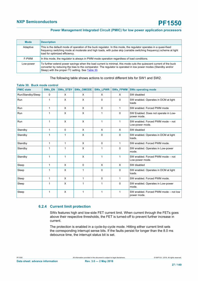
Available modes for buck regulators are presented in Table 29. These switching modesare available with OTP_SWx_DVS_SEL = 0 and OTP_SWx_DVS_SEL = 1. Table 30shows the bit settings for operating the buck converter is these modes based on thePMIC operating state.
Table 29. Buck regulator operating modesMode Description
OFF The regulator is switched off and the output voltage is discharged using an internal resistor.
NXP Semiconductors PF1550Power Management Integrated Circuit (PMIC) for low power application processors
PF1550 All information provided in this document is subject to legal disclaimers. © NXP B.V. 2018. All rights reserved.
Data sheet: advance information Rev. 3.0 — 2 May 201827 / 149
Mode Description
Adaptive This is the default mode of operation of the buck regulator. In this mode, the regulator operates in a quasi-fixedfrequency switching mode at moderate and high loads, with pulse skip (variable switching frequency) scheme at lightload for optimized efficiency.
F-PWM In this mode, the regulator is always in PWM mode operation regardless of load conditions.
Low-power To further extend power savings when the load current is minimal, this mode cuts the quiescent current of the buckconverter by reducing the bias to the comparator. The regulator is operated in low power modes (Standby and/orSleep) with the proper I2C setting. See Table 30.
The following table shows actions to control different bits for SW1 and SW2.
Table 30. Buck mode controlPMIC state SWx_EN SWx_STBY SWx_OMODE SWx_LPWR SWx_FPWM SWx operating mode
Run/Standby/Sleep 0 X X X X SW disabled
Run 1 X X 0 0 SW enabled. Operates in DCM at lightloads
Run 1 X X 0 1 SW enabled. Forced PWM mode
Run 1 X X 1 0 SW Enabled. Does not operate in Low-power mode.
Run 1 X X 1 1 SW enabled. Forced PWM mode – notLow-power mode.
Standby 1 0 X X X SW disabled
Standby 1 1 X 0 0 SW enabled. Operates in DCM at lightloads.
Standby 1 1 X 0 1 SW enabled. Forced PWM mode.
Standby 1 1 X 1 0 SW enabled. Operates in Low-powermode.
Standby 1 1 X 1 1 SW enabled. Forced PWM mode – notLow-power mode.
Sleep 1 X 0 X X SW disabled
Sleep 1 X 1 0 0 SW enabled. Operates in DCM at lightloads.
Sleep 1 X 1 0 1 SW enabled. Forced PWM mode.
Sleep 1 X 1 1 0 SW enabled. Operates in Low-powermode.
Sleep 1 X 1 1 1 SW enabled. Forced PWM mode – not lowpower mode.
6.2.4 Current limit protectionSWx features high and low-side FET current limit. When current through the FETs goesabove their respective thresholds, the FET is turned-off to prevent further increase incurrent.
The protection is enabled in a cycle-by-cycle mode. Hitting either current limit setsthe corresponding interrupt sense bits. If the faults persist for longer than the 8.0 msdebounce time, the interrupt status bit is set.

NXP Semiconductors PF1550Power Management Integrated Circuit (PMIC) for low power application processors
PF1550 All information provided in this document is subject to legal disclaimers. © NXP B.V. 2018. All rights reserved.
Data sheet: advance information Rev. 3.0 — 2 May 201828 / 149
6.2.5 Output voltage setting in SWxOutput voltage of SWx is programmable via OTP. During startup (REGS_DISABLEmode to RUN mode), contents of the OTP_SWx_VOLT[5:0] are mapped into theSWx_VOLT[5:0], SWx_STBY_VOLT[5:0] and SWx_SLP_VOLT[5:0] register which setthe regulator output voltage during Run, Standby and Sleep modes respectively.
In the DVS enabled mode (OTP_SWx_DVS_SEL = 0), values of SWx_VOLT[5:0],SWx_STBY[VOLT[5:0] and SWx_SLP_VOLT[5:0] can be changed via I2C after the PMICstarts up (RESETBMCU is released).
In the DVS disabled mode (OTP_SWx_DVS_SEL = 1), value of SWx_VOLT[5:0],SWx_STBY[VOLT[5:0] and SWx_SLP_VOLT[5:0] are read-only and must not be writtento.
Table 31. SW1 and SW2 output voltage settingSet
pointSWx_VOLT[5:0]
SWx_STBY_VOLT[5:0]SWx_SLP_VOLT[5:0]
Output voltagewith DVS enabled
OTP_SWx_DVS_SEL = 0
Output voltagewith DVS disabled
OTP_SWx_DVS_SEL = 1
0 000000 0.6000 1.10
1 000001 0.6125 1.20
2 000010 0.6250 1.35
3 000011 0.6375 1.50
4 000100 0.6500 1.80
5 000101 0.6625 2.50
6 000110 0.6750 3.00
7 000111 0.6875 3.30
8 001000 0.7000 3.30
9 001001 0.7125 3.30
10 001010 0.7250 3.30
11 001011 0.7375 3.30
12 001100 0.7500 3.30
13 001101 0.7625 3.30
14 001110 0.7750 3.30
15 001111 0.7875 3.30
16 010000 0.8000 3.3
17 010001 0.8125 3.30
18 010010 0.8250 3.30
19 010011 0.8375 3.30
20 010100 0.8500 3.30
21 010101 0.8625 3.30
22 010110 0.8750 3.30
23 010111 0.8875 3.30

NXP Semiconductors PF1550Power Management Integrated Circuit (PMIC) for low power application processors
PF1550 All information provided in this document is subject to legal disclaimers. © NXP B.V. 2018. All rights reserved.
Data sheet: advance information Rev. 3.0 — 2 May 201829 / 149
Setpoint
SWx_VOLT[5:0]SWx_STBY_VOLT[5:0]SWx_SLP_VOLT[5:0]
Output voltagewith DVS enabled
OTP_SWx_DVS_SEL = 0
Output voltagewith DVS disabled
OTP_SWx_DVS_SEL = 1
24 011000 0.9000 3.30
25 011001 0.9125 3.30
26 011010 0.9250 3.30
27 011011 0.9375 3.30
28 011100 0.9500 3.30
29 011101 0.9625 3.30
30 011110 0.9750 3.30
31 011111 0.9875 3.30
32 100000 1.0000 3.30
33 100001 1.0125 3.30
34 100010 1.0250 3.30
35 100011 1.0375 3.30
36 100100 1.0500 3.30
37 100101 1.0625 3.30
38 100110 1.0750 3.30
39 100111 1.0875 3.30
40 101000 1.1000 3.30
41 101001 1.1125 3.30
42 101010 1.125 3.30
43 101011 1.1375 3.30
44 101100 1.1500 3.30
45 101101 1.1625 3.30
46 101110 1.1750 3.30
47 101111 1.1875 3.30
48 110000 1.2000 3.30
49 110001 1.2125 3.30
50 110010 1.2250 3.30
51 110011 1.2375 3.30
52 110100 1.2500 3.30
53 110101 1.2625 3.30
54 110110 1.2750 3.30
55 110111 1.2875 3.30
56 111000 1.3000 3.30
57 111001 1.3125 3.3
58 111010 1.3250 3.30

NXP Semiconductors PF1550Power Management Integrated Circuit (PMIC) for low power application processors
PF1550 All information provided in this document is subject to legal disclaimers. © NXP B.V. 2018. All rights reserved.
Data sheet: advance information Rev. 3.0 — 2 May 201830 / 149
Setpoint
SWx_VOLT[5:0]SWx_STBY_VOLT[5:0]SWx_SLP_VOLT[5:0]
Output voltagewith DVS enabled
OTP_SWx_DVS_SEL = 0
Output voltagewith DVS disabled
OTP_SWx_DVS_SEL = 1
59 111011 1.3375 3.30
60 111100 1.3500 3.30
61 111101 1.3625 3.30
62 111110 1.3750 3.30
63 111111 1.3875 3.30
NXP Semiconductors PF1550Power Management Integrated Circuit (PMIC) for low power application processors
PF1550 All information provided in this document is subject to legal disclaimers. © NXP B.V. 2018. All rights reserved.
Data sheet: advance information Rev. 3.0 — 2 May 201831 / 149
6.2.6 SWx external componentsTable 32 shows the combination of inductor and capacitor values that work with the SWxregulator.
The design is optimized for a 1.0 µH inductor.
Table 32. Acceptable inductance and capacitance valuesInductance / capacitance 2 x 10 µF
1.0 µH
Table 33 and Table 34 show example inductor and capacitor part numbers respectively.
Table 33. Example inductor part numbersPart number Size (mm) 1.0 µHDFE201610E 2.0 x 1.6 57 mΩ, 3.6 A
DFE201610P 2.0 x 1.6 70 mΩ, 3.1 A
DFE201210U 2.0 x 1.2 95 mΩ, 3.1 A
DFE160810S 1.6 x 0.8 120 mΩ, 2.0 A
DFE201208S 2.0 x 1.2 86 mΩ, 2.4 A
DFE160808S 1.6 x 0.8 144 mΩ, 1.9 A
Table 34. Example capacitor part numbersMurata part number DescriptionGRM188R60J106ME47D 6.3 V, 10 µF, 0402, X5R
GRM188D70J106MA73 6.3 V, 10 µF, 0402, X7R
GRM188R61A106KE69 10 µF 10 V 10 % X5R 0603 .95 mm
GRM219R61A106KE44 10 µF 10 V 10 % X5R 0805 .95 mm
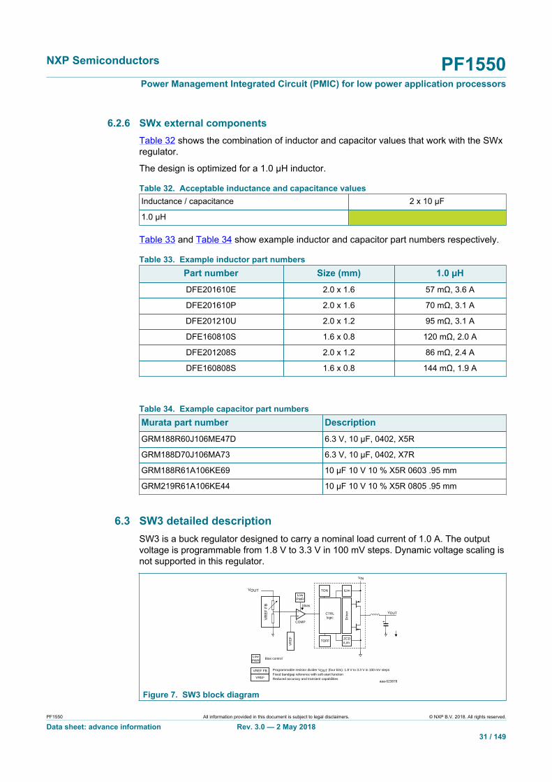
6.3 SW3 detailed descriptionSW3 is a buck regulator designed to carry a nominal load current of 1.0 A. The outputvoltage is programmable from 1.8 V to 3.3 V in 100 mV steps. Dynamic voltage scaling isnot supported in this regulator.
Programmable resistor divider VOUT (four bits): 1.8 V to 3.3 V in 100 mV stepsFixed bandgap reference with soft-start functionReduced accuracy and transient capabilities
VREF FB
VREF
Bias control
VR
EF
FB
COMP
VR
EF
LowPWR
ibias
LowPWR
VIN
VOUT
TON iLim
CTRLlogic D
river
TOFFZCDiLim
aaa-023878
VOUT
Figure 7. SW3 block diagram

NXP Semiconductors PF1550Power Management Integrated Circuit (PMIC) for low power application processors
PF1550 All information provided in this document is subject to legal disclaimers. © NXP B.V. 2018. All rights reserved.
Data sheet: advance information Rev. 3.0 — 2 May 201832 / 149
6.3.1 Regulator controlTo improve system efficiency the buck regulator can operate in different switching/bias modes. The changing between DCM/CCM takes place automatically based ondetecting the load current level. It can be enforced by one of the following means: I2Cprogramming, exiting/entering the Standby mode, exiting/entering Sleep/ Low-powermode.
Available modes for buck regulators are presented in Table 35 .
Table 36 shows the bit settings for operating the buck converter in these modes basedon the PMIC operating state.
Table 35. SW3 buck regulator operating modesMode Description
OFF The regulator is switched off and the output voltage is discharged using an internal resistor.
Adaptive This is the default mode of operation of the buck regulator. In this mode, the regulatoroperates in a quasi-fixed frequency switching mode at moderate and high loads, with pulseskip (variable switching frequency) scheme at light load for optimized efficiency.
F-PWM In this mode, the regulator is always in PWM mode operation regardless of load conditions.
Low-power To further extend power savings when the load current is minimal, this mode cuts thequiescent current of the buck converter by reducing the bias to the comparator. The regulatoris operated in low power modes (Standby and/or Sleep) with the proper I2C setting. SeeTable 36.
Table 36. SW3 buck mode controlPMIC state SW3_EN SW3_STBY SW3_OMODE SW3_LPWR SW3_FPWM SW3 operating mode
Run/Standby/Sleep
0 X X X X SW disabled
Run 1 X X 0 0 SW enabledOperates in DCM at lightloads
Run 1 X X 0 1 SW enabledForced PWM mode
Run 1 X X 1 0 SW enabledDoes not operate in Low-power mode
Run 1 X X 1 1 SW enabledForced PWM mode
Standby 1 0 X X X SW disabled
Standby 1 1 X 0 0 SW enabledOperates in DCM at lightloads
Standby 1 1 X 0 1 SW enabledForced PWM mode
Standby 1 1 X 1 0 SW EnabledOperates in Low-power mode
Standby 1 1 X 1 1 SW enabledForced PWM mode
Sleep 1 X 0 X X SW disabled

NXP Semiconductors PF1550Power Management Integrated Circuit (PMIC) for low power application processors
PF1550 All information provided in this document is subject to legal disclaimers. © NXP B.V. 2018. All rights reserved.
Data sheet: advance information Rev. 3.0 — 2 May 201833 / 149
PMIC state SW3_EN SW3_STBY SW3_OMODE SW3_LPWR SW3_FPWM SW3 operating mode
Sleep 1 X 1 0 0 SW enabledOperates in DCM at lightloads
Sleep 1 X 1 0 1 SW enabledForced PWM mode
Sleep 1 X 1 1 0 SW enabledOperates in Low-power mode
Sleep 1 X 1 1 1 SW enabledForced PWM mode
6.3.2 Current limit protectionSW3 features high and low-side FET current limit. When current through the FETs goesabove their respective thresholds, the FET is turned-off to prevent further increase incurrent.
The protection is enabled in a cycle-by-cycle mode. Hitting either current limit setsthe corresponding interrupt sense bits. If the faults persist for longer than the 8.0 msdebounce time, the interrupt status bit is set.
6.3.3 Output voltage setting in SW3Output voltage of SW3 is programmable via OTP. During start up (REGS_DISABLEmode to RUN mode), contents of the OTP_SW3_VOLT[5:0] are mapped into theSW3_VOLT[5:0], SW3_STBY_VOLT[5:0] and SW3_SLP_VOLT[5:0] register which setthe regulator output voltage during Run, Standby and Sleep modes respectively.
Values of SW3_VOLT[5:0], SW3_STBY[VOLT[5:0] and SW3_SLP_VOLT[5:0] are read-only and cannot be written to.
Table 37. SW3 output voltage settingSet point SW3_VOLT[3:0]
SW3_STBY_VOLT[3:0]SW3_SLP_VOLT[3:0]
Output voltage (V)
0 0000 1.80
1 0001 1.90
2 0010 2.00
3 0011 2.10
4 0100 2.20
5 0101 2.30
6 0110 2.40
7 0111 2.50
8 1000 2.60
9 1001 2.70
10 1010 2.80
11 1011 2.90
12 1100 3.00
13 1101 3.10

NXP Semiconductors PF1550Power Management Integrated Circuit (PMIC) for low power application processors
PF1550 All information provided in this document is subject to legal disclaimers. © NXP B.V. 2018. All rights reserved.
Data sheet: advance information Rev. 3.0 — 2 May 201834 / 149
Set point SW3_VOLT[3:0]SW3_STBY_VOLT[3:0]SW3_SLP_VOLT[3:0]
Output voltage (V)
14 1110 3.20
15 1111 3.30
6.3.4 SW3 external componentsTable 38 shows the combination of inductor and capacitor values that work with the SW3regulator.
Table 38. Acceptable inductance and capacitance valuesInductance / capacitance 2 x 10 µF
1.0 µH
Table 39 and Table 40 show example inductor and capacitor part numbers respectively.
Table 39. Example inductor part numbersPart number Size (mm) 1.0 µHDFE201610E 2.0 x 1.6 57 mΩ, 3.6 A
DFE201610P 2.0 x 1.6 70 mΩ, 3.1 A
DFE201210U 2.0 x 1.2 95 mΩ, 3.1 A
DFE160810S 1.6 x 0.8 120 mΩ, 2.0 A
DFE201208S 2.0 x 1.2 86 mΩ, 2.4 A
DFE160808S 1.6 x 0.8 144 mΩ, 1.9 A
Table 40. Example capacitor part numbersMurata part number DescriptionGRM188R60J106ME47D 6.3 V, 10 µF, 0402, X5R
GRM188D70J106MA73 6.3 V, 10 µF, 0402, X7R
GRM188R61A106KE69 10 µF 10 V 10 % X5R 0603 .95 mm
GRM219R61A106KE44 10 µF 10 V 10 % X5R 0805 .95 mm
7 Low dropout linear regulators, VREFDDR and VSNVS
7.1 General descriptionThis section describes the LDO regulators provided by the PF1550. All regulators use themain bandgap as reference.
When a regulator is disabled, the output is discharged by an internal pulldown.
VLDO1 and VLDO3 can be used as load switches by setting the corresponding LoadSwitch enable bit OTP_VLDOx_LS.

NXP Semiconductors PF1550Power Management Integrated Circuit (PMIC) for low power application processors
PF1550 All information provided in this document is subject to legal disclaimers. © NXP B.V. 2018. All rights reserved.
Data sheet: advance information Rev. 3.0 — 2 May 201835 / 149
All general purpose LDOs have short-circuit protection capability. The Short-circuitProtection (SCP) system includes de-bounced fault condition detection, regulatorshutdown, and processor interrupt generation, to contain failures and minimize thechance of product damage. If a short-circuit condition is detected and REGSCPENbit is set, the LDO is disabled by resetting its VLDOxEN bit, while at the same time,an interrupt VLDOxFAULTI is generated to flag the fault to the system processor. TheVLDOxFAULTI interrupt is maskable through the VLDOxFAULTM mask bit.
The SCP feature is enabled by setting the REGSCPEN bit. If this bit is not set, theregulators are not automatically be disabled upon a short-circuit detection. However,the current limiter continues to limit the output current of the regulator. By default, theREGSCPEN is not set; therefore, at start up none of the regulators are disabled if anoverloaded condition occurs. A fault interrupt, VLDOxFAULTI is generated in an overloadcondition regardless of the state of the REGSCPEN bit. Each LDO features a Low-powermode where the quiescent current consumed is significantly lower than in regulatoroperation. In the Low-power mode, load current of each regulator is limited to 10 mA.
7.2 LDO1 and LDO3 detailed descriptionLDO1 and LDO3 are identical 300 mA low dropout (LDO) regulators that provide outputvoltage with high accuracy and are programmable through I2C interface bits. Beingidentical, reference is made to these LDOs as LDOy.
To support this wide input range, LDOy circuit incorporates a PMOS pass FET as well asan NMOS pass FET. The LDO uses the main bandgap as its reference.
The regulator incorporates a soft-start circuit that ramps the internal reference in orderto provide smooth output waveform with minimal overshooting during power up. Whenthe regulator is disabled, the output is discharged by an internal pulldown resistor.Additionally, the LDO can be used as a load switch by setting the corresponding LoadSwitch enable bit OTP_LDOy_LS.
Moreover, LDOy includes current limit protection with the option to turn off the LDO whenan overcurrent is detected.
7.2.1 Features summary• Input range LDO from 1.0 V to 4.5 V• Programmable output voltage between 0.75 V to 1.5 V (uses NMOS) or 1.8 V and
3.3 V (uses PMOS) with 2 % accuracy• Soft-start ramp control during power up and discharge mechanism during power down• Low quiescent current (~ 2.5 µA) at Low-power mode• Current limit protection• Configurable into load switch via OTP bit

NXP Semiconductors PF1550Power Management Integrated Circuit (PMIC) for low power application processors
PF1550 All information provided in this document is subject to legal disclaimers. © NXP B.V. 2018. All rights reserved.
Data sheet: advance information Rev. 3.0 — 2 May 201836 / 149
7.2.2 LDOy block diagram
Discharge
VDD
VINx
VREF
LDOxEN
LDOxLPWR
LDOx
I2Cinterface
LDOxIN
LDOxOUT
CLDOx
aaa-023879
Figure 8. LDOy Block Diagram
7.2.3 LDOy external componentsUse a 4.7 µF X5R/X7R capacitor from output to ground with a voltage rating at least 2times the nominal output voltage.
7.2.4 LDOy output voltage settingLDOy output voltage is programmed by setting the LDOy[4:0] bits as shown in Table 41.
Table 41. LDOy output voltage settingSet point LDOy[4:0] LDOy output (V)
0 00000 0.7500
1 00001 0.8000
2 00010 0.8500
3 00011 0.9000
4 00100 0.9500
5 00101 1.0000
6 00110 1.0500
7 00111 1.1000
8 01000 1.1500
9 01001 1.2000
10 01010 1.2500
11 01011 1.3000
12 01100 1.3500
13 01101 1.4000
14 01110 1.4500
15 01111 1.5000
16 10000 1.8000

NXP Semiconductors PF1550Power Management Integrated Circuit (PMIC) for low power application processors
PF1550 All information provided in this document is subject to legal disclaimers. © NXP B.V. 2018. All rights reserved.
Data sheet: advance information Rev. 3.0 — 2 May 201837 / 149
Set point LDOy[4:0] LDOy output (V)
17 10001 1.9000
18 10010 2.0000
19 10011 2.1000
20 10100 2.2000
21 10101 2.3000
22 10110 2.4000
23 10111 2.5000
24 11000 2.6000
25 11001 2.7000
26 11010 2.8000
27 11011 2.9000
28 11100 3.0000
29 11101 3.1000
30 11110 3.2000
31 11111 3.3000
7.2.5 LDOy low power mode operationLDOy can operate in a Low-power mode with reduced quiescent current. The Low-powermode can be activated in Standby and Sleep modes by setting the LDOy_LPWR bit asshown in Table 42. Maximum load current is limited to 10 mA when operating in the Low-power mode.
Table 42. LDOy control bitsPMIC state LDOy_EN LDOy_STBY LDOy_OMODE LDOy_LPWR LDOy operating mode
Run/Standby/Sleep 0 X X X LDO disabled
Run 1 X X X LDO enabled
Standby 1 0 X X LDO disabled
Standby 1 1 X 0 LDO enabled
Standby 1 1 X 1 LDO enabled in Low-power mode
Sleep 1 X 0 X LDO disabled
Sleep 1 X 1 0 LDO enabled
Sleep 1 X 1 1 LDO enabled in Low-power mode
7.2.6 LDOy current limit protectionLDOy has built in current limit protection. When the load current exceeds the currentlimit threshold, the regulator goes from a voltage regulation mode to a current regulationmode that limits the available output current.
By setting the REGSCPEN bit, LDOy can be automatically disabled in the event ofan over current situation. In the event of an over current, the LDO will be disabledby resetting its LDOy_EN bit, while at the same time an interrupt LDOy_FAULTI isgenerated to flag the fault to the system processor. The LDOy_FAULTI interrupt ismaskable through the LDOy_FAULTM mask bit.
NXP Semiconductors PF1550Power Management Integrated Circuit (PMIC) for low power application processors
PF1550 All information provided in this document is subject to legal disclaimers. © NXP B.V. 2018. All rights reserved.
Data sheet: advance information Rev. 3.0 — 2 May 201838 / 149
If REGSCPEN is not set, the regulator will not be automatically disabled, but will insteadenter the current limit mode. By default, the REGSCPEN is not set; therefore, at start-up none of the regulators will be disabled if an overloaded condition occurs. A faultinterrupt, LDOy_FAULTI, is generated in an overload condition regardless of the state ofthe REGSCPEN bit.
Current limit is not active when LDOy is operated in the load switch mode.
7.2.7 LDOy load switch modeThe LDOy path can be turned into a switch by setting the OTP_LDOy_LS bit. Setting thisbit fully turns on the LDO pass FET. This could be useful if power domain partitioning oradditional isolation is needed on the system application. Soft-start is engaged during startup of the load switch to reduce inrush currents.
7.3 LDO2 detailed descriptionLDO2 is a 400 mA low dropout (LDO) regulator that provides output voltage with highaccuracy and programmable through I2C/ interface bits. To support this wide input rangethe LDO circuit incorporates a PMOS pass FET. The LDO uses the main bandgap as itsreference.
The regulator incorporates a soft-start circuit that ramps the internal reference in orderto provide smooth output waveform with minimal overshooting during power up. Whenthe regulator is disabled, the output is discharged by an internal pulldown resistor. Thepulldown is also activated when RESETBMCU is low.
Moreover, LDO2 includes current limit protection with option to turn off the LDO when anovercurrent is detected.
7.3.1 LDO2 features summary• Input range LDO from 2.8 V to 4.5 V• Programmable output voltage between 1.8 V and 3.3 V with 2 % accuracy• Soft-start ramp control during power up and discharge mechanism during power down• Low quiescent current (~ 1.5 µA) at Low-power mode• Current limit protection

NXP Semiconductors PF1550Power Management Integrated Circuit (PMIC) for low power application processors
PF1550 All information provided in this document is subject to legal disclaimers. © NXP B.V. 2018. All rights reserved.
Data sheet: advance information Rev. 3.0 — 2 May 201839 / 149
7.3.2 LDO2 block diagram
Discharge
VREF
LDOxEN
LDOxLPWR
LDOx
I2Cinterface
LDOxIN
LDOxIN
LDOxOUT
CLDOx
aaa-023880
Figure 9. LDO2 block diagram
7.3.3 LDO2 external componentsUse a 10 µF X5R/X7R capacitor from output to ground with a voltage rating at least 2times the nominal output voltage.
7.3.4 LDO2 output voltage settingLDO2 output voltage is programmed by setting the VLDO2[3:0] bits as shown inTable 43.
Table 43. LDO2 output voltage settingSet point VLDO2[3:0] VLDO2 output (V)
0 0000 1.80
1 0001 1.90
2 0010 2.00
3 0011 2.10
4 0100 2.20
5 0101 2.30
6 0110 2.40
7 0111 2.50
8 1000 2.60
9 1001 2.70
10 1010 2.80
11 1011 2.90
12 1100 3.00
13 1101 3.10
14 1110 3.20
15 1111 3.30

NXP Semiconductors PF1550Power Management Integrated Circuit (PMIC) for low power application processors
PF1550 All information provided in this document is subject to legal disclaimers. © NXP B.V. 2018. All rights reserved.
Data sheet: advance information Rev. 3.0 — 2 May 201840 / 149
7.3.5 LDO2 Low-power mode operationLDO2 can operate in a Low-power mode with reduced quiescent current. The low powermode can be activated in Standby and Sleep modes by setting the LDO2LPWR bit asshown in Table 44. Maximum load current is limited to 10 mA when operating in the Low-power mode.
Table 44. LDO2 control bitsPMIC state LDO2EN LDO2STBY LDO2OMODE LDO2LPWR LDO2 operating mode
Run 0 X X X LDO disabled
Run 1 X X X LDO enabled
Standby 1 0 X X LDO disabled
Standby 1 1 X 0 LDO enabled
Standby 1 1 X 1 LDO enabled in Low-power mode
Sleep 1 X 0 X LDO disabled
Sleep 1 X 1 0 LDO enabled
Sleep 1 X 1 1 LDO enabled in Low-power mode
7.3.6 LDO2 current limit protectionLDO2 has built in current limit protection. When the load current exceeds the currentlimit threshold, the regulator goes from a voltage regulation mode to a current regulationmode limiting the available output current.
By setting the REGSCPEN bit, LDO2 can be automatically disabled in the event of anover current situation. In the event of an over current, the LDO is disabled by resettingits VLDO2EN bit, while at the same time an interrupt VLDO2FAULTI is generated to flagthe fault to the system processor. The VLDO2FAULTI interrupt is maskable through theVLDO2FAULTM mask bit.
If REGSCPEN is not set, the regulator will not be automatically disabled, but insteadenter the current limit mode. By default, the REGSCPEN is not set; therefore, at start-up none of the regulators will be disabled if an overloaded condition occurs. A faultinterrupt, VLDO2FAULTI is generated in an overload condition regardless of the state ofthe REGSCPEN bit.
7.4 VREFDDR referenceVREFDDR is an internal NMOS half supply voltage follower capable of supplying upto 10 mA. The output voltage is at one half the input voltage. It is typically used as thereference voltage for DDR memories.
A filtered resistor divider is utilized to create a low frequency pole. This divider thenutilizes a voltage follower to drive the load.

NXP Semiconductors PF1550Power Management Integrated Circuit (PMIC) for low power application processors
PF1550 All information provided in this document is subject to legal disclaimers. © NXP B.V. 2018. All rights reserved.
Data sheet: advance information Rev. 3.0 — 2 May 201841 / 149
Discharge
VINREFDDR
VINREFDDR
VREFDDRVREFDDR
CREFDDR
aaa-023881
1.0 µF
Figure 10. VREFDDR block diagram
7.5 VSNVS LDO/SwitchVSNVS powers the low-power SNVS/RTC domain on the processor. It derives its powerfrom either VSYS or a coin cell (only if the COIN_CELL bit is set). When powered byboth, VSYS powers VSNVS if VSYS > VTH threshold and LICELL powers VSNVS whenVSYS < VTL. When powered by VSYS, VSNVS is an LDO capable of supplying 2.0mA at 3.0 V. When powered by coin cell, VSNVS output tracks the coin cell voltage bymeans of a switch. In this case, the VSNVS voltage is simply the coin cell voltage minusthe voltage drop across the switch.
Upon subsequent removal of VSYS, with the coin cell attached and COIN_CELL set,VSNVS will change configuration from an LDO to a switch.
aaa-023882
LDO/LOAD switch
Inputsense
selector
I2C interface
VSNVS
VSYS
Coin cellcharger
1.8 to 3.3 V
PF1550
Coin cell
VREF
Figure 11. VSNVS block diagram

NXP Semiconductors PF1550Power Management Integrated Circuit (PMIC) for low power application processors
PF1550 All information provided in this document is subject to legal disclaimers. © NXP B.V. 2018. All rights reserved.
Data sheet: advance information Rev. 3.0 — 2 May 201842 / 149
8 Battery charger description
The PF1550 charger is an integrated 1-cell Li+ charger with a single VBUS power inputand dual path output. All power switches for charging and switching the load betweenbattery and external power are included on chip. No external MOSFETs, blocking diodesor current sense resistors are required.
The VBUS input operates from 4.0 V to 6.5 V with up to 22 V overvoltage protection. ThePF1550 internally blocks current from the battery and system back to the inputs when noinput supply is present. Other features include precharge battery conditioning and timer,fast charge timer, battery overvoltage protection, charge status and fault outputs, batterythermistor monitor and thermal regulation.
Figure 12 shows a high level internal block diagram of the charger block. The PMIC ispowered from the VSYS node in the PF1550.
VBUSIN5.0 V 37
39
4
1.8 V
VDDIO
3
1
9
SCL
4.2 V
2 SDA
INTB
WDI
2.2 F25 V0603
3.3 V1.0 F6.3 V0603
0.1 F6.3 V0603
4.7 K0402
1.0 F6.3 V0603
4.7 F10 V0603
3.7 VLi-ion
CC charge100 mA to
1.0 A
10 K0402
100 K0402
100 K0402
4.7 K0402
USBPHY
CC_CHARGE
CHARGER
I_PRECHARGE
DPM_THRESHOLD
I_EOC
3
3
1
3
3
2
5
PHY LDOVOUTENABLE
6.5 VLDO 5
622
35
36
5
OVP VSYS_MIN
LED driver
Linear charger+
BATFET control
6 CV_CHARGE
V_PRECHARGE_THRESHOLD
WEAK_BATTERY _THRESHOLD
RESTART _THRESHOLD
Battery pack
10 K thermistor
t
5
5
2
2
2
2
1
1
FAU
LTS
1
1
REG_TEMP
CC_ADJ EPAD
THM
CV_ADJ
THM_HOT
THM_WARM
THM_COOL
THM_COLD
VSYS1 VSYS
CV charge3.5 V to 4.44 V
VSYS2
40CHGB
VBUS_ILIMIT
LED_CURRENTLED_FREQLED_PWM
VFB
ILIM
HIGH VOLTAGEBLOCKINGLDO MOSFET
aaa-023883
BATTERYISOLATIONMOSFET
CC TIMER
PRECHARGE TIMER
EOC TIMER
WATCHDOG
CC_TIMEOUT
PRECHARGE_TIMEOUT
EOC_TIMEOUT
ENABLE
33
34
38
32
GND
VBATT1
VBATT2
2P7 supplyINT_2P7
22 F10 V0603
22 F10 V0603
47 0402
LED
I2C
INTE
RFA
CE
Controllogic
+I2C
registers
THER
MAL
TIM
ERS
VDPM
IBAT
T
VBATT
+
T
-
Figure 12. Battery charger internal block diagram

NXP Semiconductors PF1550Power Management Integrated Circuit (PMIC) for low power application processors
PF1550 All information provided in this document is subject to legal disclaimers. © NXP B.V. 2018. All rights reserved.
Data sheet: advance information Rev. 3.0 — 2 May 201843 / 149
8.1 Operating modes and behavioral description
VBATT
TSSVBUS_LIN
VBUSIN
INT2P7
VBUS_VALID
BGOK
VSYS
VCORE
VCOREDIG
VBUS_ILIM
USBPHY(3.3 V)
VDDIO
Chargerdetection
0 V
1.8 VCommandedby processor
VSYSMIN4.3 V
SLEEP
SLEEP
0x00 (100 mA) Based onadaptor type
Processor detection sequence SLEEP
aaa-025039
Linear on
Default mode OTPselectable (linear on
or charger on)
Externalsupply
Charger onCharger
state
INT2P7
0 V
Startup sequence, USB insert, VBATT = 0 V
5.0 V
1.5 V
1.5 V
> 100 ms (min)
Figure 13. Charger low battery (Startup sequence, USB insert, VBATT = 0 V)

NXP Semiconductors PF1550Power Management Integrated Circuit (PMIC) for low power application processors
PF1550 All information provided in this document is subject to legal disclaimers. © NXP B.V. 2018. All rights reserved.
Data sheet: advance information Rev. 3.0 — 2 May 201844 / 149
VBATT
VBUSIN
INT2P7
VBUS_VALID
VSYS
VDDIO
VCORE
VCOREDIG
VBUS_ILIM
USBPHY(3.3 V)
Chargerdetection
0 V
1.8 V
VSYSMIN4.3 V
SLEEP
SLEEP
0x00 (100 mA) Based onadaptor type
Processor detection sequence SLEEP
aaa-025040
Linear on
Default mode OTPselectable (linear on
or charger on)
Externalsupply
Charger onCharger
state
3.8 V
Startup sequence, USB insert, VBATT = 3.8 V
5.0 V
2.7 V
1.5 V
1.5 V
3.8 V
> 100 ms (min)
Figure 14. Charger healthy battery (Startup sequence, USB insert, VBATT = 3.8 V)
Table 45. Battery regulation voltage registerBATTERY REGULATION VOLTAGE REGISTER
ADDR: 0x8F
D7 D6 D5 D4 D3 D2 D1 D0
BITS: VSYSMIN CHGCV
POR: 0 0 1 0 1 0 1 1
ACCESS:
The VSYSMIN value is programmable via OTP as per the table below.

NXP Semiconductors PF1550Power Management Integrated Circuit (PMIC) for low power application processors
PF1550 All information provided in this document is subject to legal disclaimers. © NXP B.V. 2018. All rights reserved.
Data sheet: advance information Rev. 3.0 — 2 May 201845 / 149
Table 46. VSYSMIN settingVSYSMIN[1:0] setting VSYSMIN setting (V)
00 3.5
01 3.7
10 4.3
11 Reserved
The VSYSMIN setting is the "normal" regulation point for VSYS. This parameter sets thepoint where the VSYS loop starts taking control and regulates the output. 4.3 V is therecommended setting to ensure that there is enough headroom before reaching UVDET(PMIC undervoltage detection, 2.9 V typ.).
Selecting lower settings causes the VSYS loop to start regulating, and reduces chargingcurrent to lower the VSYS threshold, thus reducing the headroom.
Typically, the VSYS output range can go as low as 300 mV below the VSYSMIN setting.Therefore, the recommended setting for the VSYS output should be between 4.0 V to 4.3 V.
8.2 Charger input source detectionThe charger input is compared with several voltage thresholds to determine if it is valid. Acharger input must meet the following three characteristics to be valid:
• VBUS must be above VUVLO (4.2 V max.) to be valid• VBUS must be below its overvoltage lockout threshold (VOVLO (6.0 V min.))• VBUS must be above the system voltage by VIN2SYS (50 mV / 175 mV programmable
via OTP)
The VBUS input generates an input interrupt when its status changes. The input statuscan be read with VBUS_OK and VBUS_SNS registers. Interrupts can be masked withVBUS_M register.
Note: Adaptor removal is defined as VBUS < VUVLO.
VBUS_xx
VBUS_xx
SYS
VVBUS_xx_OVLO
VIN2SYS
VVBUS_xx_UVLO
VBUS_UVLO
VBUS_xx_INVLDVBUS_xx_OVLO
LIN2SYS
VBUS_INVLD
aaa-025038
Figure 15. Input source detection delay
8.3 Input self-discharge for reliable charger input interruptTo ensure that a rapid removal and re-insertion of a charge source always results in acharger input interrupt, the charger input presents loading to the input capacitor to ensurethat when the charge source is removed the input voltage decays below the UVLOthreshold in a reasonable time.

NXP Semiconductors PF1550Power Management Integrated Circuit (PMIC) for low power application processors
PF1550 All information provided in this document is subject to legal disclaimers. © NXP B.V. 2018. All rights reserved.
Data sheet: advance information Rev. 3.0 — 2 May 201846 / 149
A 2.2 µF input capacitance charged up to the maximum OVLO threshold (VOVLO) decaysdown to the minimum UVLO threshold within 300 ms (tINSD). The input self-discharge isimplemented by with a 30 kΩ resistor (RINSD) from VBUSIN input to ground. The inputself-discharge resistor is deactivated in the low-power mode to reduce total quiescentcurrent.
8.4 Charger state diagram
WATCHDOG SuspendWDT_SNS = 1CHG_OK = 0
ICHG = 0
WD Timer > tWD(CHG Timer = Suspend,
only if WDTEN = 1)
WDTCLR=TRUE(WD Timer = 0 & ResumeCHG Timer = Resume)
From: any prequal state, any fast charge state, end-of-charge, done or timer fault
Returns to: the same state that it came from
Battery overvoltageBAT_SNS = 0x09
BAT_OK = 0ICHG = 0
VBATT > VBATOVFor time > tBATOV
VBATT < VBATOV(Resume charge timer)
From: any precharge state, any fast charge state, end-of-charge, done
Returns to: the same state that it came from
From: any precharge state, any fast charge state, end-of-charge, done
Returns to: the same state that it came from
Battery Thermistor Suspend ModeCHG_SNS = 0x07
CHG_OK = 0ICHG = 0
Battery Temperature > THOTORBattery Temperature < TCOLD
Battery Temperature < THOTANDBattery Temperature > TCOLD(Resume charge timer)
NO INPUT POWER orCHARGER DISABLED
CHG_SNS = 0x08CHG_OK = 0
ICHG = 0CHG Timer = 0WD Timer = 0
INPUT is VALID(VBUS_VALID = 1)
and MODE PROGRAMMEDFOR CHARGER ENABLED
(CHG Timer = Start)
CHG_OPER[3:0]PROGRAMMED THE
CHARGER TO BE OFF
INPUT isINVALID
ANY STATEexcept thermal
shutdownTJ < TSHDN
(CHG Timer = SuspendWD Timer = Suspend)
DirectTransition
TJ > TSHDN(CHG Timer = 0WD Timer = 0)
Thermal ShutdownCHG_SNS = 0x0A
CHG_OK = 0ICHG = 0
CHG Timer > tPRECHG
LOW-BATTERYPRECHARGE MODE
CHG_SNS = 0x00CHG_OK = 1
ICHG ≤ IPRECHG.LB
VBATT < VPRECHG.LB(CHG Timer = 0)
VBATT > VPRECHG.LB(Soft Start, CHG Timer = 0)
TIMER FAULTCHG_SNS = 0x06
CHG_OK = 0ICHG = 0
FAST CHARGE (CC)CHG_SNS = 0x01
CHG_OK = 1VBATT ≤ VBATREG
ICHG ≤ IFC and ICHG > IEOC
FAST CHARGE (CV)CHG_SNS = 0x02
CHG_OK = 1ICHG ≤ IFC and ICHG > IEOC
VBATT <95 % of VBATREG
VBATT = 99 % of VBATREG for 32 ms
CHG Timer > tFC
CHG Timer > tFC
ICHG < IEOC for tSCIDG(CHG Timer = 0 and Suspend)
END-OF-CHARGECHG_SNS = 0x03
CHG_OK = 1ICHG ≤ IEOC
CHG Timer > tEOC
DONECHG_SNS = 0x04
CHG_OK = 0ICHG = 0
VBATT < (VBATREG - VRESTART)(No Soft Start,
CHG Timer = Restart)
VBATT < (VBATREG - VRESTART)(No Soft Start,
CHG Timer = Restart)
aaa-025042
Figure 16. Charger state diagram

NXP Semiconductors PF1550Power Management Integrated Circuit (PMIC) for low power application processors
PF1550 All information provided in this document is subject to legal disclaimers. © NXP B.V. 2018. All rights reserved.
Data sheet: advance information Rev. 3.0 — 2 May 201847 / 149
8.5 Charging profileThe battery is charged in three modes as shown below. Linear control of the BATFEThas two subset modes (Trickle and Linear constant current mode).
• Linear control of BATFET– Trickle (programmable from 55 mA/100 mA based on battery voltage)– Linear constant current mode from 100 mA to 1000 mA
• Constant current (CC)• Constant voltage (CV)
aaa-023884
VBATREGVRESTART
VLOW_BATT
ICHARGE_CC
IPRECHARGEIEOC
Stat
eB
atte
rycu
rren
tB
atte
ryvo
ltage
Low
batte
ryre
cove
ry
Batte
rydi
scon
nect
ed
Fast chargeconstant voltage (CV)
Fast chargeconstant current (CC)
Time
Time
End-
of-c
harg
e(E
OC
)
End-
of-c
harg
e(E
OC
)
DO
NE
(VSY
Slo
aded
)
Res
tart
fast
char
ge(C
V)
VSYS
VBATT (> 0 V)
IBAT (0 A)
Figure 17. Charging profile
8.5.1 Precharge stateThe precharge state is entered when the main-battery voltage is less thanVPRECHG.LB which is precharge (low battery) charging voltage threshold set byPRECHGLB_THRS[6:5]. After being in this state for tSCIDG, a CHG_I interrupt isgenerated, CHG_OK bit is set and CHG_SNS register is set to 0x00. In the prechargestate, the charge current into the battery is equal or lower than IPRECHG.LB (45 mA typ).
Following events causes the state machine to exit this state:
1. When the main battery voltage rises above VPRECHG.LB, the charger enters the nextstate in the charging cycle: “Fast-Charge Constant Current" state.
2. If the battery charger remains in this state for longer than tPRECHG, the charger statemachine transitions to the “Timer Fault” state.

NXP Semiconductors PF1550Power Management Integrated Circuit (PMIC) for low power application processors
PF1550 All information provided in this document is subject to legal disclaimers. © NXP B.V. 2018. All rights reserved.
Data sheet: advance information Rev. 3.0 — 2 May 201848 / 149
3. If the watchdog timer is not serviced, the charger state machine transitions to the“Watchdog Suspend” state.
Note: The precharge state works with battery voltages down to 0 V.
The low 0 V operation typically allows this battery charger to revive batteries that havean “open” internal pack protector. Typically, the pack internal protection circuit isolatesthe Lithium-ion cell if the battery pack has detected an overcurrent, undervoltage orovervoltage. When a battery with an “open” internal pack protector is used with thischarger, the low-battery precharge mode forces a small current into the 0 V battery. Thiscurrent raises the pack’s terminal voltage above the pack revive threshold, causing thepacks internal pack protection switch to reconnect the Lithium-ion cell.
Note that a normal battery pack typically could stay in the low-battery precharge state forseveral minutes. If a battery pack stays in low-battery precharge for longer than tPRECHG,it may be defective.
8.5.2 Fast charge constant current stateThe fast-charge constant current (CC) state occurs when the main-battery voltage isgreater than the precharge threshold and less than the battery regulation threshold(VPRECHG.LB < VBATT < VCHGCV). In the fast-charge CC state the current into the battery isless than or equal to IFC (excluding accuracy IFCACC).
Charge current may be less than IFC for any of the following reasons:
• The charger input is in input current limit• The charger input voltage is low• The system load is consuming adapter current. When the voltage drop between VBUS
and VSYS is below the VIN2SYS threshold, charging stops and charge current dropsdown to 0 A.
Note: The system load always gets priority over the battery charge current.
Note that the system load always gets priority over the battery charge current.
The following events cause the state machine to exit this state:
• When the main battery voltage rises above VBATREG, the charger enters the next statein the charging cycle: "Fast Charge (CV)".
• If the battery charger remains in this state for longer than tFC, the charger statemachine transitions to the "Timer Fault" state.
• If the watchdog timer is not serviced, the charger state machine transitions to the"Watchdog Suspend" state.
The battery charger dissipates the most power in the fast-charge constant current state.This power dissipation causes the internal die temperature to rise. If the die temperatureexceeds the threshold set by REGTEMP[1:0], IFC is reduced. This is covered in thermalregulation section.

NXP Semiconductors PF1550Power Management Integrated Circuit (PMIC) for low power application processors
PF1550 All information provided in this document is subject to legal disclaimers. © NXP B.V. 2018. All rights reserved.
Data sheet: advance information Rev. 3.0 — 2 May 201849 / 149
Table 47. Charger current control registerCHARGER CURRENT CONTROL REGISTER
ADDR: 0x8E
D7 D6 D5 D4 D3 D2 D1 D0
BITS: RESERVED PRECHGLB_THRESHOLD CHG_CC
POR: 0 0 0 0 0 0 0 0
ACCESS: —
The fast charge current is programmable via I2C using the bits shown below.
Table 48. Constant current charge settingsCHG_CC[4:0] setting IFC current (mA)
00000 100
00001 150
00010 200
00011 250
00100 300
00101 350
00110 400
00111 450
01000 500
01001 550
01010 600
01011 650
01100 700
01101 750
01110 800
01111 850
10000 900
10001 950
10010 1000
10011 1050 (Reserved)
10100 1100 (Reserved)
10101 1150 (Reserved)
10110 1200 (Reserved)
10111 1250 (Reserved)
11000 1300 (Reserved)
11001 1350 (Reserved)
11010 1400 (Reserved)
11011 1450 (Reserved)
11100 1500 (Reserved)
11101 1550 (Reserved)
11110 1600 (Reserved)

NXP Semiconductors PF1550Power Management Integrated Circuit (PMIC) for low power application processors
PF1550 All information provided in this document is subject to legal disclaimers. © NXP B.V. 2018. All rights reserved.
Data sheet: advance information Rev. 3.0 — 2 May 201850 / 149
CHG_CC[4:0] setting IFC current (mA)
11111 1650 (Reserved)
To insure proper operation, the maximum CC current selected must be one setting belowinput current limit (in charger normal mode).
In normal mode, when VSYS < VSYSMINLOOPx (VSYSMINLOOPx = VSYSMINx − 300 mV), digitallogic automatically controls maximum CC current (one setting lower than charger inputcurrent limit ILIM setting). If 100 mA input current limit is selected, the charge current isforced to 50 mA to allow enough current for VSYS.
The Charger Low-power mode (CLPM) is entered automatically when the 50 mA inputcurrent limit setting, or lower, is selected and when VBATT > 2.8 V.
8.5.3 Fast charge constant voltage stateThe fast-charge constant voltage (CV) state occurs when the battery voltage rises toVBATREG from the fast-charge CC state.
In the fast-charge CV state, the battery charger maintains VBATREG across the batteryand the charge current is less than or equal to IFC. Charger current decreasesexponentially in this state as the battery becomes fully charged.
The BATFET control circuitry may reduce the charge current for any of the followingreasons:
• The charger input is in input current limit• The charger input voltage is low• The system load is consuming adapter current. Note that the system load always gets
priority over the battery charge current.
The following events cause the state machine to exit this state:
• When the charger current is below IEOC for tSCIDG, the charger enters the next state inthe charging cycle: “End-of-Charge”.
• If the battery charger remains in this state for longer than tFC, the charger statemachine transitions to the “Timer Fault” state.
• If the watchdog timer is not serviced, the charger state machine transitions to the“Watchdog Suspend” state.
Note: During the CC to CV transition, the charge current can be momentarily higherthan IFC. This current is safe and does not result in over charging the battery. After thistransition, the charge current decays and is less than or equal to IFC.
Table 49. Battery regulation voltage registerBATTERY REGULATION VOLTAGE REGISTER
ADDR: 0x8F
D7 D6 D5 D4 D3 D2 D1 D0
BITS: VSYSMIN CHGCV
POR: 0 0 1 0 1 0 1 1
ACCESS:
The CV setting is programmable via I2C using the bits below.

NXP Semiconductors PF1550Power Management Integrated Circuit (PMIC) for low power application processors
PF1550 All information provided in this document is subject to legal disclaimers. © NXP B.V. 2018. All rights reserved.
Data sheet: advance information Rev. 3.0 — 2 May 201851 / 149
Table 50. CV settingsCHGCV[5:0] Output voltage (V)
000000 3.50
000001 3.50
000010 3.50
000011 3.50
000100 3.50
000101 3.50
000110 3.50
000111 3.50
001000 3.50
001001 3.52
001010 3.54
001011 3.56
001100 3.58
001101 3.60
001110 3.62
001111 3.64
010000 3.66
010001 3.68
010010 3.70
010011 3.72
010100 3.74
010101 3.76
010110 3.78
010111 3.80
011000 3.82
011001 3.84
011010 3.86
011011 3.88
011100 3.90
011101 3.92
011110 3.94
011111 3.96
100000 3.98
100001 4.00
100010 4.02
100011 4.04
100100 4.06
100101 4.08
100110 4.10
100111 4.12
NXP Semiconductors PF1550Power Management Integrated Circuit (PMIC) for low power application processors
PF1550 All information provided in this document is subject to legal disclaimers. © NXP B.V. 2018. All rights reserved.
Data sheet: advance information Rev. 3.0 — 2 May 201852 / 149
CHGCV[5:0] Output voltage (V)
101000 4.14
101001 4.16
101010 4.18
101011 [1] 4.20
101100 4.22
101101 4.24
101110 4.26
101111 4.28
110000 4.30
110001 4.32
110010 4.34
110011 4.36
110100 4.38
110101 4.40
110110 4.42
110111 4.44
111000 4.44
111001 4.44
111010 4.44
111011 4.44
111100 4.44
111101 4.44
111110 4.44
111111 4.44
[1] Default setting
Table 51. Charger timers registerCHARGER TIMERS REGISTER
ADDR: 0x8A
D7 D6 D5 D4 D3 D2 D1 D0
BITS: TPRECHG RESERVED EOCTIME FCHGTIME
POR: 0 0 0 0 1 0 1 0
ACCESS: —
The fast charge timer is programmable via I2C through the below bits:
Table 52. Fast charge timer settingsFCHGTIME[2:0] setting Fast charge timer duration (Hours)
000 Disable
001 2
010 4

NXP Semiconductors PF1550Power Management Integrated Circuit (PMIC) for low power application processors
PF1550 All information provided in this document is subject to legal disclaimers. © NXP B.V. 2018. All rights reserved.
Data sheet: advance information Rev. 3.0 — 2 May 201853 / 149
FCHGTIME[2:0] setting Fast charge timer duration (Hours)
011 6
100 8
101 10
110 12
111 14
Note that, the fast charge timer fault can occur in the fast charge mode, the systemdraws current such that the charger state machine is technically in the "fast charge" statebut the battery is not really in "fast charge". This can happen if the current available fromthe charger input is not sufficient to provide system load as well as charge the battery.It is up to the processor to react to the timer fault accordingly. It can decide to re-startcharging (via CHG_OPER), or accept it as an actual timer fault.
8.5.4 End-of-charge stateThe end-of-charge state can only be entered from the fast-charge CV state when thecharger current decreases below IEOC for tSCIDG. After being in the top-off state for tSCIDG+ tDB(EOC), an interrupt is generated, CHG_OK is set and CHG_SNS = 0x03. In the end-of-charge state, the battery charger tries to maintain VCHGCV across the battery andtypically the charge current is less than or equal to IEOC.
The BATFET control circuitry may reduce the charge current lower than the battery mayotherwise consume for any of the following reasons:
• The charger input is in input current limit• The charger input voltage is low• The system load is consuming adapter current. Note that the system load always gets
priority over the battery charge current.
The following events cause the state machine to exit this state:
• After being in this state for the end-of-charge time (tEOC), the charger enters the nextstate in the charging cycle: “DONE”.
• If VBATT < VBATREG – VRESTART, the charger goes back to the “FAST CHARGE (CC)”state.
• If the watchdog timer is not serviced, the charger state machine transitions to the“Watchdog Suspend” state.
Table 53. Charger EOC configuration registerCHARGER EOC CONFIGURATION REGISTER
ADDR: 0x8D
D7 D6 D5 D4 D3 D2 D1 D0
BITS: EOC_MODE IEOC EOC_EXIT FRC_BATT_ISO
CHG_RESTART
POR: 0 1 0 0 0 0 0 1
ACCESS:
The EOC current value is programmable per the below table:

NXP Semiconductors PF1550Power Management Integrated Circuit (PMIC) for low power application processors
PF1550 All information provided in this document is subject to legal disclaimers. © NXP B.V. 2018. All rights reserved.
Data sheet: advance information Rev. 3.0 — 2 May 201854 / 149
Table 54. EOC current thresholdsIEOC[2:0] setting IEOC current (mA)
000 5
001 10
010 20
011 30
100 50
101 Reserved
110 Reserved
111 Reserved
Table 55. Charger timers registerCHARGER TIMERS REGISTER
ADDR: 0x8A
D7 D6 D5 D4 D3 D2 D1 D0
BITS: TPRECHG RESERVED EOCTIME FCHGTIME
POR: 0 0 0 0 1 0 1 0
ACCESS: —
The EOC State timer is programmable per below table:
Table 56. EOC state timer settingsEOCTIME[2:0] setting EOC timer duration (Minutes)
000 0 (16 seconds debounce)
001 10
010 20
011 30
100 40
101 50
110 60
111 70
8.5.5 Done stateThe battery charger enters its done state after the charger has been in the end-of-charge state for tEOC. After being in this state for tSCIDG, a CHG_I interrupt is generated,CHG_OK is cleared and CHG_SNS = 0x04.
The following events cause the state machine to exit this state:
• If VBATT < VBATREG – VRESTART, the charger goes back to the "FAST CHARGE (CC)"state
• If the watchdog timer is not serviced, the charger state machine transitions to the"Watchdog Suspend" state
In the done state, the charge current into the battery (ICHG) is 0 A. In the done state,the charger presents a very light load to the battery. If the system load presented to the

NXP Semiconductors PF1550Power Management Integrated Circuit (PMIC) for low power application processors
PF1550 All information provided in this document is subject to legal disclaimers. © NXP B.V. 2018. All rights reserved.
Data sheet: advance information Rev. 3.0 — 2 May 201855 / 149
battery is low (<<100 µA), then a typical system can remain in the done state for manydays.
If left in the done state long enough, the battery voltage decays below the restartthreshold (VRESTART) and the charger state machine transitions back into the fast-charge CC state. There is no soft start (di/dt limiting) during the done to fast-charge statetransition. In the DONE state, the BATFET is fully closed. The correct way to triggerrestart feature is to pull loading from VSYS, in order to discharge VBATT.
8.6 Battery supplement modeThe Battery supplement mode is a powerful feature of the PF1550 charger, allowing thedevice to temporarily suspend charging, and draw supplemental current from the batteryto maintain power to the system when the load demands more current than the VBUSsupply can deliver. This permits users more flexibility when architecting their system. Thebattery capacity can be chosen to handle periods of peak loading, which may be currentshigher than supported by the VBUS supply.
If the system load current exceeds the VBUS input current limit, the VSYS supply currentis no longer be able to support the load demand and the VSYS output voltage decreases.When VSYS falls below VBATT the PF1550 suspends charging and enters the Batterysupplement mode. In this mode, the battery provides current to support the VSYS loaddemand.
If the load demand on VSYS now decreases, the VSYS output voltage recovers,and begins to rise. When VSYS rises above VBATT, the PF1550 exits the Batterysupplement mode and resumes charging the battery in the CC charging phase.
When VBATT decreases lower than the restart threshold, the part enters CC state fromDONE. Then if the loading on VSYS decreases and VSYS > VBATT, charger starts tocharge from the CC state.
8.7 Power path features
8.7.1 VSYS regulationIn the case of a low battery, the LDO path regulates VSYS to either 3.5 V, 3.7 V or 4.3 V.This allows the system to power up with a low battery while the battery gets charged. SeeTable 46.
8.7.2 Input current limitThe default settings of the VBUSIN and CHG_OPER control bits are such that when acharge source is applied to VBUSIN, the PF1550 turns its linear regulator on in LINEAR-ON or CHARGE-ON (via OTP), and limits the charge current to 100 mA (via OTP).
See Section 12 "Register map" for the default values for specific registers/bits.
The input current limit works by monitoring the current being drawn from the input andcomparing it to the programmed current limit. The current limit should be set based onthe current-handling capability of the input adaptor. Generally, this limit is chosen tooptimally fulfill the system-power requirements while achieving a satisfactory chargingtime for the batteries. If the adaptor current exceeds its output capability, the charger
NXP Semiconductors PF1550Power Management Integrated Circuit (PMIC) for low power application processors
PF1550 All information provided in this document is subject to legal disclaimers. © NXP B.V. 2018. All rights reserved.
Data sheet: advance information Rev. 3.0 — 2 May 201856 / 149
responds by reducing the charger current, thereby keeping the current drawn from theadaptor within its capability.
There is a precision current sense circuitry that monitors the input current wheneverinternal INT_2P7 is asserted. The input current limit logic signal is used to reducequiescent current when the charger is not plugged in by turning off the current senseamplifier. The input current limit should include current consumed by the charger block.
There is a low-power mode for the linear regulator where it consumes less than 2.5 mAbias current at 25 °C. This is useful for the 10 mA to 50 mA input current limit settings.
The input current limit also includes a second control which is voltage based. Whenit drops below the desired input, it generates an interrupt to decrease the fast-chargecurrent. This is further covered in input voltage regulation mode.
Table 57. VBUS input current limit registerVBUS INPUT CURRENT LIMIT REGISTER
ADDR: 0x94
D7 D6 D5 D4 D3 D2 D1 D0
BITS: VBUS_LIN_ILIM RESERVED
POR: 0 1 1 0 1 0 0 0
ACCESS: R/W R/W R/W R/W R/W —
The table below shows valid input current limit settings.
Table 58. Input current limit settingsVBUS_LIN_ILIM[4:0] setting VBUS input current limit (mA)
00000 10
00001 15
00010 20
00011 25
00100 30
00101 35
00110 40
00111 45
01000 50
01001 100
01010 150
01011 200
01100 300
01101 400
01110 500
01111 600
10000 700
10001 800
10010 900
10011 1000
10100 1500

NXP Semiconductors PF1550Power Management Integrated Circuit (PMIC) for low power application processors
PF1550 All information provided in this document is subject to legal disclaimers. © NXP B.V. 2018. All rights reserved.
Data sheet: advance information Rev. 3.0 — 2 May 201857 / 149
VBUS_LIN_ILIM[4:0] setting VBUS input current limit (mA)
10101 to 11101 Reserved
11110 Reserved
11111 Reserved
8.7.3 Battery thermistorThermistor is not supported when there is no valid charger inserted. A bank ofcomparators monitors the thermistor to provide battery temperature information forthe battery charger. The comparator thresholds are based on the recommended NTCNCP15XH103F03RC (10 K) from Murata or equivalent. Each comparator has 3 #hysteresis. There are I2C selections for the THOT and TCOLD temperature threshold.
8.7.4 BATFET soft startWhen the battery is first plugged into the PF1550, BATFET features an internal soft-startthat prevent high inrush currents into the capacitors at the VSYS node.
Note: This feature must be tested during lab validation for functionality. It is not requiredto cover this in production as there are no critical pass/fail criteria for this feature.
8.8 Thermal
8.8.1 Thermal regulationThermal regulation maximizes the battery charge current while regulating the PF1550junction temperature. The target charge current reduction is achieved with a digitalcontrol loop. As shown in figure below, when the die temperature exceeds the valueprogrammed by REGTEMP[1:0], a thermal limiting circuit reduces the battery charger’starget current.
Cur
rent
(%
)
80 °C
Junction temperature (°C)
95 °C 110 °C 125 °C
IFC = 100%
IFC = 50%
IFC = 25%
IFC = 12.5%
100 %
50 %
25 %
12.5 %
100 mA
aaa-025043
Figure 18. Thermal regulation

NXP Semiconductors PF1550Power Management Integrated Circuit (PMIC) for low power application processors
PF1550 All information provided in this document is subject to legal disclaimers. © NXP B.V. 2018. All rights reserved.
Data sheet: advance information Rev. 3.0 — 2 May 201858 / 149
Table 59. Thermal regulationREGTEMP[1:0] 50 % CC
Thermalregulation setpoint (TJREG0)
25 % CCThermal
regulation setpoint (TJREG1)
12.5 % CCThermal
regulation setpoint (TJREG2)
100 mA CCThermal
regulation setpoint (TJREG3)
00 80 °C 95 °C 110 °C 125 °C
01 95 °C 110 °C N/A 125 °C
10 110 °C N/A N/A 125 °C
11 N/A N/A N/A 125 °C
As shown in figure below, a hysteresis mechanism is implemented.
Cur
rent
(%
)
80 °C
Junction temperature (°C)
95 °C 110 °C 125 °C
75 °C 90 °C 105 °C 120 °C
IFC = 100%
IFC = 50%
IFC = 25%
IFC = 12.5%
100 %
50 %
25 %
12.5 %
100 mA
aaa-025044
Figure 19. Thermal regulation (Current versus Temp, example with REGTEMP[1:0] = 00 andhysteresis
When thermal regulation changes state, a THM_I interrupt is generated. This is to allowthe system’s microprocessor time to read the status of the thermal regulation loop via theTREG_SNS status bit.
This diagram below shows an example of the thermal regulation over time. The greenarrows represent when the CHG_I interrupt is generated.
Cur
rent
(%
)
80 °C
Time (s)
75 °C
25 °C
IFC = 100%
IFC = 50%
aaa-025045
Figure 20. Thermal regulation (Current, Temp versus Time, example with REGTEMP[1:0] =00 and hysteresis
The thermal regulation does not affect the CHG_OK bit (only information contained withinCHG_SNS affects CHG_OK).

NXP Semiconductors PF1550Power Management Integrated Circuit (PMIC) for low power application processors
PF1550 All information provided in this document is subject to legal disclaimers. © NXP B.V. 2018. All rights reserved.
Data sheet: advance information Rev. 3.0 — 2 May 201859 / 149
8.8.2 Thermal foldbackThe thermal foldback function reduces max. charging current which goes into the batterywhen the charger junction temperature (TJREGx) reaches a pre-defined temperature setby REGTEMP[1:0]. Note that the thermal foldback loop being active is not considered tobe an abnormal condition.
After the temperature reaches TJREG0, the charging current will be reduced to 50 % of thefinal CC charging current value.
After the charger temperature rises above TJREG0, if the charger temperature falls backbelow TJREG0 − 5 °C, charging current reverts back to 100 % of the final CC chargingcurrent value.
If the charger temperature rises and reaches TJREG1 but below 125 °C, charging currentis reduced to 25 % of the final CC charging current value.
After the charger temperature rises above TJREG1, if the charger temperature falls backbelow TJREG1 − 5 °C, charging current reverts back to 50 % of the final CC chargingcurrent value.
If the charger temperature rises and reaches TJREG2 but below 125 °C, charging currentis reduced to 12.5 % of the final CC charging current value.
After the charger temperature rises above TJREG2, if the charger temperature falls backbelow TJREG2 − 5 °C, charging current reverts back to 25 % of the final CC chargingcurrent value.
If the charger temperature reaches 125 °C, charging current is reduced to 100 mA.
After the charger temperature rises above 125 °C, if the charger temperature falls backbelow 120 °C, charging current reverses back to 12.5 % of the final CC charging currentvalue.
The thermal foldback function is not available for LPM.
At charger junction temperature above TJREGx, if the charger current is already set to100 mA, the thermal foldback function keeps the current 100 mA. The final chargingcurrent min. out of the fold back function is clamped at 100 mA.
Table 60. Temperature regulation control registerTEMPERATURE REGULATION CONTROL REGISTER
ADDR: 0x92
D7 D6 D5 D4 D3 D2 D1 D0
BITS: TEMP_FB_EN RESERVED THM_HOT THM_COLD REGTEMP THM_CONFIG
POR: 0 0 0 0 0 1 0 1
ACCESS: —
The table below shows the different thermal regulation set point:
Table 61. Thermal regulation settingsREGTEMP[1:0] setting Thermal regulation set point (°C)
00 80
01 95
10 110
11 Reserved

NXP Semiconductors PF1550Power Management Integrated Circuit (PMIC) for low power application processors
PF1550 All information provided in this document is subject to legal disclaimers. © NXP B.V. 2018. All rights reserved.
Data sheet: advance information Rev. 3.0 — 2 May 201860 / 149
8.8.3 Input voltage regulation modeAn input-voltage regulation loop allows the charger to be well behaved when it isattached to a poor quality power source. The loop improves performance with relativelyhigh resistance charge sources that exist when long cables are used or devices arecharged with non-compliant USB hub configurations. Additionally, this input-voltageregulation loop improves performance with current limited adapters. If the input currentlimit is programmed above the current limit threshold of given adapter, the input voltageloop allows regulation at the current limit of the adapter. Finally, the input-voltageregulation loop allows the charger to perform well with adapters that have poor transientload response times.
The input-voltage regulation loop automatically reduces the input current limit in order tokeep the input voltage at VVBUS_DPM_REG. Once VBUS drops to the 4.5 V threshold (thisthreshold itself is selectable via the VBUS_DPM_REG[2:0] bits), the charging currentis scaled back and this brings back the VBUS voltage higher. The Dynamic PowerManagement (DPM) loop then regulates the charging current (indirectly by reducinginput current limit) dynamically to maintain VBUS at the DPM threshold. An interrupt isgenerated after the debounce time to notify the processor of the DPM event.
In the figure below, VBUS starts to drop as the charging current increases.
aaa-023886
4.5 V
4.3 V
VUVLO (falling)
Charge current
VBUS voltage
VBUS_DPM interrupt
INTB
tINTDEB
VBUS_D PM threshold (falling)
VBUS_D PM_STOP threshold
Figure 21. Response to input voltage droop during charging
The next figure below describes a more stringent event.

NXP Semiconductors PF1550Power Management Integrated Circuit (PMIC) for low power application processors
PF1550 All information provided in this document is subject to legal disclaimers. © NXP B.V. 2018. All rights reserved.
Data sheet: advance information Rev. 3.0 — 2 May 201861 / 149
4.5 V
4.3 V
Charge current
CC_Charge current incremented
1 LSB
VBUS voltage
VBUS_DPM threshold (falling)
VBUS_DPM_STOP threshold
2.0 µs
10 ms
10 ms
200 mV
100 mA
aaa-025041
Figure 22. DPM function
There is a second comparator in the DPM loop which is set 200 mV below theVBUS_DPM_REG threshold. As seen in the second figure above, if the VBUS voltagecontinues to drop and hits the threshold of the second comparator, the charging currentis immediately brought to the 100 mA setting to recover from the input voltage droop. Atthis point, the VBUS voltage should recover (assuming current drawn from VSYS is notcausing the VBUS collapse).
Now, the charging current is stepped up slowly (every 10 ms) to arrive at the maximumvalue that allows regulation of VBUS to or slightly above the DPM threshold. At everyincrementing step, the digital logic monitors if the VBUS voltage is above the 4.5 Vcomparator. The incrementing continues only if it is.
Table 62. VBUS linear dynamic input voltage registerVBUS LINEAR DYNAMIC INPUT VOLTAGE REGISTER
ADDR: 0x95
D7 D6 D5 D4 D3 D2 D1 D0
BITS: RESERVED VIN_DPM_STOP PRECHGDBATT_THRESHOLD VBUS_DPM_REG_VOLTAGE
POR: 0 0 0 0 0 0 0 0
ACCESS: —
The input DPM voltage regulation set point is selected by writing to the VBUS_REGregister.
Table 63. Input voltage regulation thresholdsVBUS_REG[2:0] setting VBUS DPM REG voltage setting (V)
000 3.9
001 4.0
010 4.1
011 4.2
100 4.3
101 4.4
110 4.5

NXP Semiconductors PF1550Power Management Integrated Circuit (PMIC) for low power application processors
PF1550 All information provided in this document is subject to legal disclaimers. © NXP B.V. 2018. All rights reserved.
Data sheet: advance information Rev. 3.0 — 2 May 201862 / 149
VBUS_REG[2:0] setting VBUS DPM REG voltage setting (V)
111 4.6
8.8.4 JEITA thermal controlThe PF1550 includes a temperature control function that conforms to therecommendations specified in the Japan Electronics and Information TechnologyIndustries Association (JEITA) guidelines for improving the safety when charging oflithium-ion batteries.
The JEITA specification establishes five temperature zones, COLD, COOL, NORMAL,WARM, and HOT, with four temperature thresholds partitioning the zones. Batterytemperature is monitored using a NTC thermistor, in close proximity of the cell, and thecharger is carefully controlled as shown in the following table:
Table 64. JEITA thermal controlZone JEITA control functionCOLD Charging inhibited
COOL Charger CC current and CV voltage adjusted
NORMAL No JEITA control
WARM Charger CC current and CV voltage adjusted
HOT Charging inhibited
JEITA Thermal Control is enabled by selecting bits THM_CNFG[1:0] in the TemperatureRegulation and Control Register 0x92.
Table 65. Temperature regulation control registerTEMPERATURE REGULATION CONTROL REGISTER
ADDR: 0x92
D7 D6 D5 D4 D3 D2 D1 D0
BITS: TEMP_FB_EN RESERVED THM_HOT THM_COLD REGTEMP THM_CONFIG
POR: 0 0 0 0 0 1 0 1
ACCESS: —
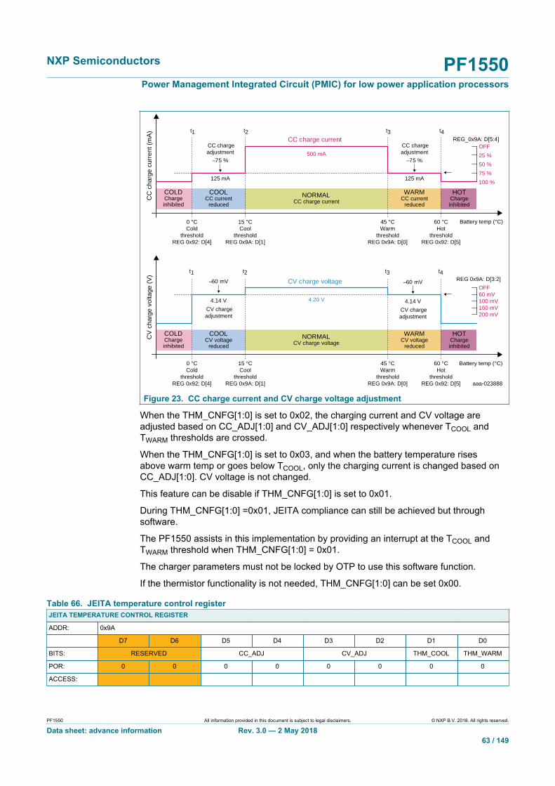
NXP Semiconductors PF1550Power Management Integrated Circuit (PMIC) for low power application processors
PF1550 All information provided in this document is subject to legal disclaimers. © NXP B.V. 2018. All rights reserved.
Data sheet: advance information Rev. 3.0 — 2 May 201863 / 149
COOLCV voltage
reduced
NORMAL CV charge voltage
WARM CV voltage
reduced
HOT Charge inhibited
COLDCharge inhibited
t2
0 °C Cold
threshold REG 0x92: D[4]
15 °C Cool
threshold REG 0x9A: D[1]
45 °C Warm
threshold REG 0x9A: D[0]
60 °C Hot
threshold REG 0x92: D[5]
CV charge adjustment
CV charge voltage
200 mV
60 mV
–60 mV
4.20 V4.14 V
CV charge adjustment
–60 mV
4.14 V
Battery temp (°C)
CV
cha
rge
volta
ge (
V)
OFF
100 mV160 mV
t1 t3 t4
t2t1 t3 t4
REG 0x9A: D[3:2]
aaa-023888
0 °C Cold
threshold REG 0x92: D[4]
15 °C Cool
threshold REG 0x9A: D[1]
45 °C Warm
threshold REG 0x9A: D[0]
60 °C Hot
threshold REG 0x92: D[5]
CC charge adjustment
CC charge current
100 %
25 %–75 %
500 mA
125 mA
CC charge adjustment
–75 %
125 mA
Battery temp (°C)
CC
cha
rge
curr
ent (
mA
)OFF
50 %
75 %
REG_0x9A: D[5:4]
COOLCC current
reduced
NORMAL CC charge current
WARM CC current
reduced
HOT Charge inhibited
COLDCharge inhibited
Figure 23. CC charge current and CV charge voltage adjustment
When the THM_CNFG[1:0] is set to 0x02, the charging current and CV voltage areadjusted based on CC_ADJ[1:0] and CV_ADJ[1:0] respectively whenever TCOOL andTWARM thresholds are crossed.
When the THM_CNFG[1:0] is set to 0x03, and when the battery temperature risesabove warm temp or goes below TCOOL, only the charging current is changed based onCC_ADJ[1:0]. CV voltage is not changed.
This feature can be disable if THM_CNFG[1:0] is set to 0x01.
During THM_CNFG[1:0] =0x01, JEITA compliance can still be achieved but throughsoftware.
The PF1550 assists in this implementation by providing an interrupt at the TCOOL andTWARM threshold when THM_CNFG[1:0] = 0x01.
The charger parameters must not be locked by OTP to use this software function.
If the thermistor functionality is not needed, THM_CNFG[1:0] can be set 0x00.
Table 66. JEITA temperature control registerJEITA TEMPERATURE CONTROL REGISTER
ADDR: 0x9A
D7 D6 D5 D4 D3 D2 D1 D0
BITS: RESERVED CC_ADJ CV_ADJ THM_COOL THM_WARM
POR: 0 0 0 0 0 0 0 0
ACCESS:

NXP Semiconductors PF1550Power Management Integrated Circuit (PMIC) for low power application processors
PF1550 All information provided in this document is subject to legal disclaimers. © NXP B.V. 2018. All rights reserved.
Data sheet: advance information Rev. 3.0 — 2 May 201864 / 149
CV_ADJ[1:0] has four settings subtraction off of CHGCV[5:0] settings, refer to registermap and TBBOTP:
Table 67. CV voltage adjustment settingsCV_ADJ[1:0] CV voltage adjustment (mV)
00 60
01 100
10 160
11 200
CC_ADJ[1:0] has four settings subtraction off of CHG_CC settings, see register map andTBBOTP:
Table 68. CC current adjustment settingsCC_ADJ[1:0] CC current adjustment (%)
00 25 %
01 50 %
10 75 %
11 100 %
THM_HOT[0] THM_HOT setting (#)
0 60
1 55
THM_COLD[0] THM_COLD setting (#)
0 0
1 -10
8.9 Fault states
8.9.1 Timer fault stateThe battery charger provides both a charge timer and a watchdog timer to ensure safecharging.
The charge timer prevents the battery from charging indefinitely. The time that thecharger is allowed to remain in its each of its pre-qualification states is tPRECHG.
The time that the charger is allowed to remain in the fast-charge CC and CV states is tFCwhich is programmable with FCHGTIME.
Finally, the time that the charger is in the end-of-charge state is tEOC which isprogrammable with EOCTIME bits. Upon entering the timer fault state, a CHG_I interruptis generated without a delay, CHG_OK is cleared and CHG_SNS = 0x06.
In the timer fault state, the charger is off. The charger can exit the timer fault state byprogramming the charger to be off and then programming it to be on again through theCHG_OPER bits. Alternatively, the charger input can be removed and re-inserted to exitthe timer fault state.
VSYS should continue to regulate while in the Timer fault state.

NXP Semiconductors PF1550Power Management Integrated Circuit (PMIC) for low power application processors
PF1550 All information provided in this document is subject to legal disclaimers. © NXP B.V. 2018. All rights reserved.
Data sheet: advance information Rev. 3.0 — 2 May 201865 / 149
8.9.2 Watchdog timer stateThe battery charger provides both a charge timer and a watchdog timer to ensure safecharging. The watchdog timer protects the battery from charging indefinitely in the eventthat the host hangs or otherwise cannot communicate correctly.
The watchdog timer is disabled by default with WDTEN = 0. To use the watchdog timerfeature, enable the feature by setting WDTEN. While enabled, the system controller mustreset the watchdog timer within the timer period (tWD) for the charger to operate normally.
Reset the watchdog timer by programming WDTCLR = 0x01. As long as WDTEN = 1, thetimer continues to run and the processor continues to clear the register before the timerexpires.
The system processor clears the WDTEN bit to stop the timer.
If the watchdog timer expires while the charger is in precharge mode, fast charge CCor CV, end-of-charge, done, or timer fault, the charging stops, a CHG_I interrupt isgenerated without a delay, CHG_OK is cleared, and CHG_SNS = 0x0B and indicatesthat the charger is off because the watchdog timer has expired.
Once the watchdog timer has expired, the charger is restarted by programmingWDTCLR=0x01. The VSYS node is supported by the battery and/or the adapter throughthe Linear regulator while the watchdog timer is expired.
8.9.3 Thermal shutdown stateThe thermal shutdown state occurs when the battery charger is in any state and thejunction temperature (TJ) exceeds the device’s thermal shutdown threshold (TSHDN),typical 140 °C.
When TJ is close to TSHDN the charger folds back the charging current to 0 A, so thecharger is effectively off. Upon entering this state, CHG_I interrupt is generated withouta delay, CHG_OK is cleared. In the thermal shutdown state, the charger is off and timersare suspended.
CHG_SNS = 0x0A and CHG_OK = 0 in the thermal shutdown state. The chargerexits the temperature suspend state and returns to the state it came from once the dietemperature has cooled. The timers resume once the charger exits this state. VSYScontinues to regulate while in the thermal shutdown state.
8.9.4 Battery overvoltage stateA battery overvoltage fault occurs in any state when the battery voltage exceeds toVBATOV threshold.
In this state, BAT_SNS = 0x09 and BAT_OK = 0. A BATT_I interrupt is generated inthis state. In the event of a battery overvoltage state, the BATFET is opened and VSYSis regulated using the linear path. Once the battery overvoltage condition clears, thecharger exits the battery overvoltage state and returns to the state it came from.
8.9.5 Charger fault prioritySome of the charger fault states occurs at the same time. For example, batteryovervoltage and thermal shutdown occurs at the same time. In this section, which failurestates take priority is discussed.

NXP Semiconductors PF1550Power Management Integrated Circuit (PMIC) for low power application processors
PF1550 All information provided in this document is subject to legal disclaimers. © NXP B.V. 2018. All rights reserved.
Data sheet: advance information Rev. 3.0 — 2 May 201866 / 149
In any given state, non-recoverable faults such as battery overcurrent timer fault take thehighest priority. Recoverable faults such as a thermistor suspend, or battery overvoltagetake lower priority.
8.9.6 Battery overcurrent limitThe VBATT to VSYS detector (BATFET) generates an overcurrent (OVRC) and providesthe signal to the PMIC on/off controller.
This feature protects the battery and the system from potential damage due to excessivebattery discharge current. Excessive battery discharge current may occur for severalreasons such as exposure to moisture, a software problem, a device failure, ormechanical failure that causes a short-circuit.
The battery overcurrent protection feature is enabled with BATFET_OC[1:0] bit.
Disabling this feature reduces the main battery current consumption. When the batterycurrent to system exceeds the programmed overcurrent threshold for at least tBOVCRI,a BAT2SOC_I interrupt is generated and BATTOC_SNS bit reports an overcurrentcondition.
If the overcurrent persists for tBOVCR, the VBATT to VSYS MOSFET is disabled or keptalive depending on the BOVRC_DISBATFET OTP bit. Typically, when the system’sprocessor detects this overcurrent interrupt, it executes a housekeeping routine that triesto mitigate the overcurrent situation. There is an OTP option (via BOVRC_DISBATFETbit) to either disable the BATFET after completion of housekeeping routine or remain on.
Batteryovercurrent
Batteryovercurrent
interrupt
VSYS VSYS shuts down
tBOVCRI = 3.0 ms
aaa-023885
tBOVCR = 16 ms
Figure 24. Response to battery overcurrent
The table below shows the different overcurrent threshold settings:
Table 69. Battery overcurrent thresholdsBATFET_OC[1:0] setting VBATT to VSYS overcurrent threshold (A)
00 Disabled
01 2.2
10 2.8
11 3.2

NXP Semiconductors PF1550Power Management Integrated Circuit (PMIC) for low power application processors
PF1550 All information provided in this document is subject to legal disclaimers. © NXP B.V. 2018. All rights reserved.
Data sheet: advance information Rev. 3.0 — 2 May 201867 / 149
8.10 LED indicatorCHGB is a 6.0 mA LED current sink with programmable blink timing. Blink period andon-time are programmable with 2-bits. The LED has indicator depending on the chargerstate as shown in the LED modes table. Blink frequency is programmable for 0.5 Hz, 1.0Hz, 8.0 Hz or 256 Hz.. Blink duration is programmable from 0/32 duty cycle to 32/32 dutycycle in 1/32 increments.
The LED_CFG bit allows the LED’s to operate in two modes as shown in the tablebelow. With LED_CFG=0 the LED’s behave as follows: charging (on), fault (flashing),and charge complete (off). When LED_CFG = 1, the LED’s have the following behavior,charging (flashing), fault (on), and charge complete (off). The LED’s are activatedautomatically when charging is started and remain under control of the state machine.Software can take control over the charge LED’s by setting the LEDOVRD = 1. WhenLEDOVRD = 1 the LEDs are totally controlled by software, therefore the state machineno longer has control. With LEDOVRD = 0 software cannot force the LED’s on but canstill set the current.
The charging LED drivers include ramp up and ramp down patterns implemented inhardware. The ramp itself is generated by increasing or decreasing the PWM duty cyclewith a 1/32 step every 1/64 seconds. The ramp time is therefore a function of the initialset PWM cycle and the final PWM cycle. As an example, starting from 0/32 and going to32/32 takes 500 ms whereas going to from 8/32 to 16/32 takes 125 ms.
Note that the ramp function is executed upon every change in PWM cycle setting.If a PWM change is programmed via I2C when LED_RAMP = 0, then the change isimmediate rather than spread out over a PWM sweep. In addition, programmable blinkrates are provided. Blinking is obtained by lowering the PWM repetition rate of each ofthe drivers through LED_FREQ[1:0] while the on period is determined by the duty cyclesetting. To avoid high frequency spur coupling in the application, the switching edges ofthe output drivers are softened.
Table 70. LED modesCondition LED_CFG = 1 LED_CFG = 0 (default) Current (mA)
Charger off Off Off 6
Charging Flashing 1.0 Hz50 % duty cycle
On steady100 % duty cycle
6
Charging fault On steady100 % duty cycle
Flashing 1.0 Hz50 % duty cycle
6
Charge complete Off Off 6
Table 71. LED enable conditionsLED_EN CHGB LEDOVRD
0 (default) Auto 0
1 On 1
0 Off 1
NXP Semiconductors PF1550Power Management Integrated Circuit (PMIC) for low power application processors
PF1550 All information provided in this document is subject to legal disclaimers. © NXP B.V. 2018. All rights reserved.
Data sheet: advance information Rev. 3.0 — 2 May 201868 / 149
Table 72. LED frequency settingLED_FREQ[1:0] Frequency Units
00 (default) 1 Hz
01 0.5 Hz
10 256 Hz
11 8 Hz
9 Control and interface signals
The PF1550 PMIC is fully programmable via the I2C interface. Additional communicationis provided by direct logic interfacing including interrupt and reset pins as well as pins forpower buttons.
9.1 PWRONPWRON is an input signal to the IC that acts as an enable signal for the voltageregulators in the PF1550.
The PWRON pin can be configured as either a level sensitive input (OTP_PWRON_CFG= 0), or as an edge sensitive input (OTP_PWRON_CFG = 1).
As a level sensitive input, an active high signal turns on the part and an active low signalturns off the part, or puts it into Sleep mode.
As an edge sensitive input, such as when connected to a mechanical switch, a fallingedge will turn on the part and if the switch is held low for greater than or equal to 4.0seconds, the part turns off or enters Sleep mode.
Table 73. PWRON pin OTP configuration optionsOTP_PWRON_CFG Mode
0 PWRON pin HIGH = ONPWRON pin LOW = OFF or Sleep mode
1 PWRON pin pulled LOW momentarily = ONPWRON pin LOW for 4.0 seconds = OFF or Sleep mode
Table 74. PWRON pin logic levelPin name Parameter Load condition Min. Max. Unit
VIL — 0.0 0.4 VPWRON
VIH — 1.4 3.6 V
When OTP_PWRON_CFG = 1, PWRON pin pulled low momentarily takes the systemfrom REGS_DISABLE/SLEEP to RUN mode. There is no effect if PWRON is pulled lowmomentarily while in RUN or STANDBY modes. Only an interrupt is generated.
PWRON pin low for 4.0 seconds with PWRONRSTEN bit = 1: Enters REGS_DISABLE orSleep mode.
See Section 10 "PF1550 state machine" for detailed description.
In this configuration, the PWRON input can be a mechanical switch de-bounced througha programmable de-bouncer, PWRONDBNC[1:0], to avoid a response to a very short key

NXP Semiconductors PF1550Power Management Integrated Circuit (PMIC) for low power application processors
PF1550 All information provided in this document is subject to legal disclaimers. © NXP B.V. 2018. All rights reserved.
Data sheet: advance information Rev. 3.0 — 2 May 201869 / 149
press. The interrupt is generated for both the falling and the rising edge of the PWRONpin. By default, a 31.25 ms interrupt debounce is applied to both falling and risingedges. The falling edge debounce timing can be extended with PWRONDBNC[1:0]. Theinterrupt is cleared by software, or when cycling through the REGS_DISABLE mode.
Table 75. PWRONDBNC settingsBits State Turn on
debounce (ms)Falling edge INTdebounce (ms)
Rising edge INTdebounce (ms)
00 31.25 31.25 31.25
01 31.25 31.25 31.25
10 125 125 31.25
PWRONDBNC[1:0]
11 750 750 31.25
9.2 STANDBYSTANDBY is an input signal to the IC. When it is asserted the part enters standby modeand when deasserted, the part exits standby mode. STANDBY can be configured asactive high or active low using the STANDBYINV bit.
Table 76. Standby pin polarity controlSTANDBY (pin) STANDBYINV (I2C bit) STANDBY control
0 0 Not in Standby mode
0 1 In Standby mode
1 0 In Standby mode
1 1 Not in Standby mode
Table 77. STANDBY pin logic levelPin name Parameter Load condition Min. Max. Unit
VIL — 0 0.2 * VSNVS VSTANDBY
VIH — 0.8 * VSNVS 3.6 V
Since STANDBY pin activity is driven asynchronously to the system, a finite timeis required for the internal logic to qualify and respond to the pin level changes. Aprogrammable delay is provided to hold off the system response to a Standby event. Thisallows the processor and peripherals some time after a standby instruction has beenreceived to terminate processes to facilitate seamless entering into Standby mode. Whenenabled (STANDBYDLY = 01, 10, or 11), STANDBYDLY delays the Standby initiatedresponse for the entire IC, until the STBYDLY counter expires. An allowance should bemade for three additional 32 kHz cycles required to synchronize the Standby event.
9.3 RESETBMCURESETBMCU is an open-drain, active low output configurable via OTP for two modes ofoperation.
In its default mode, it is deasserted at the end of the start-up sequence. In this mode, thesignal can be used to bring the processor out of reset (POR), or as an indicator that allsupplies have been enabled; it is only asserted during a turn off event.

NXP Semiconductors PF1550Power Management Integrated Circuit (PMIC) for low power application processors
PF1550 All information provided in this document is subject to legal disclaimers. © NXP B.V. 2018. All rights reserved.
Data sheet: advance information Rev. 3.0 — 2 May 201870 / 149
When configured for its fault mode, RESETBMCU is deasserted after the startupsequence is completed only if no faults occurred during start up. At any time, if a faultoccurs and persists for 1.8 ms typically, RESETBMCU is asserted low.
The PF1550 is turned off if the fault persists for more than 100 ms typically. The PWRONsignal restarts the part, though if the fault persists, the sequence described above isrepeated. To enter the fault mode, set bit OTP_PWRGD_EN to 1.
The time from the last regulator in the start-up sequence to when RESETBMCU isdeasserted is programmable between 2.0 ms and 1024 ms via OTP_POR_DLY[2:0] bits.
9.4 INTBINTB is an open-drain, active low output. It is asserted when any interrupt occurs,provided that the interrupt is unmasked. INTB is deasserted after the fault interrupt iscleared by software, which requires writing a “1” to the interrupt bit.
Each interrupt can be masked by setting the corresponding mask bit to a 1. As a result,when a masked interrupt bit goes high, the INTB pin does not go low. A masked interruptcan still be read from the interrupt status register. This gives the processor the option ofpolling for status from the IC.
The IC powers up with all interrupts masked, so the processor must initially poll thedevice to determine if any interrupts are active. Alternatively, the processor can unmaskthe interrupt bits of interest. If a masked interrupt bit was already high, the INTB pin goeslow after unmasking. The sense registers contain status and input sense bits so thesystem processor can poll the current state of interrupt sources. They are read only, andnot latched or clearable.
9.5 WDIWDI is an input signal to the IC. It is typically connected to the watchdog output of theprocessor. When the WDI pin is pulled low, the PMIC enters the “REGS_DISABLE”mode where all the regulators are turned off. The WDI acts as a hard reset input from theprocessor.
During PMIC startup (REGS_DISABLE to RUN mode), the WDI pin is masked tillRESETBMCU is deasserted.
Table 78. WDI pin logic levelPin name Parameter Load condition Min. Max. Unit
VIL — 0 0.2 * VDDIO VWDI
VIH — 0.8 * VDDIO 3.6 V
9.6 ONKEYONKEY is an input pin to the IC and is typically connected to a push-button switch. TheONKEY pin is pulled high when the switch is depressed, and is pulled low when theswitch is pressed.
Pressing the switch generates interrupts which the processor uses to initiate PMICstate transitions. Pressing the ONKEY for longer than the delay programmedby OTP_TGRESET[1:0] (ranges from 4.0 s to 16 s), forces the PMIC into theREGS_DISABLE state.

NXP Semiconductors PF1550Power Management Integrated Circuit (PMIC) for low power application processors
PF1550 All information provided in this document is subject to legal disclaimers. © NXP B.V. 2018. All rights reserved.
Data sheet: advance information Rev. 3.0 — 2 May 201871 / 149
Table 79. ONKEY pin logic levelPin name Parameter Load condition Min. Max. Unit
VIL — 0 0.2 * VBATT VONKEY
VIH — 0.8 * VBATT 3.6 V
Table 80. ONKEYDBNC settingsBits State Turn On
Debounce (ms)Falling Edge INTDebounce (ms)
Rising Edge INTDebounce (ms)
00 31.25 31.25 31.25
01 31.25 31.25 31.25
10 125 125 31.25
ONKEYDBNC[1:0]
11 750 750 31.25
The ONKEY input can be a mechanical switch debounced through a programmabledebouncer, ONKEYDBNC[1:0], to avoid a response to a very short (unintentional) keypress. The interrupt is generated during the rising edge of the ONKEY pin.
The falling edge debounce timing can be extended with ONKEYDBNC[1:0] asdefined Table 80. The interrupt is cleared by software, or when cycling through theREGS_DISABLE mode.
See Section 12 "Register map" for detailed description of the ONKEY interrupt registers.
9.7 Control interface I2C block descriptionThe PF1550 contains an I2C interface port which allows access by a processor, orany I2C master, to the register set. Via these registers, the resources of the IC can becontrolled. The registers also provide status information about how the IC is operating.
The SCL and SDA lines should be routed away from noisy signals and planes tominimize noise pick up. To prevent reflections in the SCL and SDA traces from creatingfalse pulses, the rise and fall times of the SCL and SDA signals must be greater than20 ns. This can be accomplished by reducing the drive strength of the I2C master viasoftware.
9.7.1 I2C device IDI2C interface protocol requires a device ID for addressing the target IC on a multi-devicebus. The PF1550 I2C device address is 0x08.
9.7.2 I2C operationThe I2C mode of the interface is implemented generally following the fast mode definitionwhich supports up to 400 kbits/s operation (exceptions to the standard are noted to be7-bit only addressing and no support for general call addressing). Timing diagrams,electrical specifications, and further details can be found in the I2C specification, which isavailable for download at:
http://www.nxp.com/acrobat_download/literature/9398/39340011.pdf

NXP Semiconductors PF1550Power Management Integrated Circuit (PMIC) for low power application processors
PF1550 All information provided in this document is subject to legal disclaimers. © NXP B.V. 2018. All rights reserved.
Data sheet: advance information Rev. 3.0 — 2 May 201872 / 149
I2C read operations are also performed in byte increments separated by an ACK. Readoperations also begin with the MSB and each byte is sent out unless a STOP commandor NACK is received prior to completion.
The following examples show how to write and read data to and from the IC. The hostinitiates and terminates all communication. The host sends a master command packetafter driving the start condition. The device responds to the host if the master commandpacket contains the corresponding slave address. In the following examples, the deviceis shown always responding with an ACK to transmissions from the host. If at any timea NACK is received, the host should terminate the current transaction and retry thetransaction.
SDA
I2C write example
I2C read example
S 0
device address register address master driven data
acknowledgefrom slave
acknowledgefrom slave
acknowledgefrom slave
START condition STOPcondition
host can also driveanother STARTinstead of STOP
PAA DATA (byte 0)A
R/W
SDA S 0
device address device addressregister address PMIC driven data
acknowledgefrom slave
acknowledgefrom slave
no acknowledgefrom slave
START condition
S
START condition STOPcondition
host can also driveanother STARTinstead of STOP
PNAAA
R/W
1
acknowledgefrom slave
A
R/W
aaa-026501
Figure 25. I2C sequence
10 PF1550 state machine
The PMIC part of the PF1550 can operate in a number of states as shown in Figure 26.
The states can be split into two categories:
1. “System On” that includes the RUN, STANDBY and SLEEP modes2. “System Off” that includes the REGS_DISABLE, CORE_OFF and SHIP modes
STANDBY RUN
SLEEP/LPSR
System running, VCOREDIG ON
AB
C FE
H
G
L
I
J
KREGS_DISABLE(VSNVS from VSYS
or LICELL)(MBATT ON,
VCOREDIG ON)SHIP
(MBATT OFF,VCOREDIG OFF,
VSNVS OFF)
CORE_OFFVSNVS_ONLY
(VSNVS from VSYSor LICELL)
(MBATT ON,VCOREDIG OFF)
aaa-023889
Figure 26. PMIC state machine
In the “System On” modes, some or all of the PMIC regulators are powered and ingeneral the system processor is powered.
In the “System Off” modes, all (or all regulators except VSNVS) are powered off. Ingeneral the system processor is powered off during these states. In the REGS_DISABLE

NXP Semiconductors PF1550Power Management Integrated Circuit (PMIC) for low power application processors
PF1550 All information provided in this document is subject to legal disclaimers. © NXP B.V. 2018. All rights reserved.
Data sheet: advance information Rev. 3.0 — 2 May 201873 / 149
and CORE_OFF modes, the VSNVS supply remains enabled keeping the system RTCrunning.
The only way to transition from “System Off” to “System On” and vice versa is throughthe REGS_DISABLE mode. From the REGS_DISABLE mode, the only exit into a“System On” state is into the “Run” mode. Transition from the REGS_DISABLE mode tothe Run mode requires a Turn On event. See Section 10.3 "Turn on events".
Transition from any of the “System On” modes to the REGS_DISABLE state is allowed.This transition is referred to as a Turn Off event. See Section 10.4 "Turn off events".
10.1 System ON states
10.1.1 Run stateIn this state, the PMIC regulators are enabled and the system is powered up.RESETBMCU is de-asserted in this state.
This mode can be entered in several ways:
1. From REGS_DISABLE through a Turn On Event: During this transition, the PMICregulators are powered up as per their programmed start-up sequence. After all theregulators are powered, the RESETBMCU pin is de-asserted.
2. From STANDBY by using the STANDBY pin3. From SLEEP mode by using the PWRON pin: Typically, some of the regulators are
turned off in the SLEEP mode compared to the RUN mode. In the SLEEP mode,some of the buck regulator output voltages are set lower than those in the RUNmode. While transitioning from the SLEEP to the RUN mode, regulators that wereturned off in the SLEEP mode are turned back on in the RUN mode following thesame sequence as the programmed OTP sequence. Output voltage transitions duringtransition from the SLEEP to the RUN mode also occurs at the same OTP sequencetime slot. RESETBMCU is de-asserted through this state transition.
10.1.2 STANDBY stateThis state is entered by controlling the logic level of the STANDBY pin. It can be enteredonly from the RUN mode.
The STANDBY pin polarity is programmable through the STANDBYINV I2C bit. Bydefault, STANDBYINV = 0 and a logic high on the STANDBY pin moves the statemachine from the RUN state to the STANDBY state. When STANDBYINV = 1, a logiclow moves the state machine from the RUN state to the STANDBY state.
Regulator output voltage may be changed, or regulator outputs could be disabled whileentering the STANDBY state and vice versa.
For details on the power-down sequence, see Section 10.7 "Regulator power-downsequencer". While exiting STANDBY state into the RUN mode, regulator output voltagechanges and regulator enables follow the power-up sequence.
It is possible to exit STANDBY state and enter the SLEEP state. SLEEP state isgenerally a lower power system state compared to the STANDBY state. ExitingSTANDBY into the SLEEP state follows the power-down sequence.
RESETBMCU is de-asserted in the STANDBY state.

NXP Semiconductors PF1550Power Management Integrated Circuit (PMIC) for low power application processors
PF1550 All information provided in this document is subject to legal disclaimers. © NXP B.V. 2018. All rights reserved.
Data sheet: advance information Rev. 3.0 — 2 May 201874 / 149
10.1.3 SLEEP stateThis state is entered from either the RUN state or the STANDBY state by controllingthe PWRON pin. The exact condition required for this transition depends on the OTPconfiguration of the PWRON pin. For details see Section 9.1 "PWRON".
The power-down sequence is followed while entering this state and the power-upsequence is followed while exiting this state into the RUN state.
RESETBMCU is de-asserted in the SLEEP state.
10.2 System OFF statesRESETBMCU is asserted (low) in all the System Off states.
10.2.1 REGS_DISABLEThis state can be considered the ‘home state’ for the state machine. In this state, thestate machine waits for appropriate commands to proceed to other states.
REGS_DISABLE can be entered from one of the “System On” state through a turn offevent.
REGS_DISABLE can be entered from the CORE_OFF and SHIP mode by pressing theONKEY button for more than 1000 ms or by a charger attach event.
In the REGS_DISABLE state, the PMIC core circuitry is active. VSNVS is a best-of-supply output of VSYS and LICELL.
10.2.2 CORE_OFFThis state is entered in two ways:
1. From the REGS_DISABLE mode by pressing and holding the ON_KEY button low >Tgreset
2. From the REGS_DISABLE mode if the GOTO_CORE_OFF bit is set
This state cannot be entered if a charger is plugged in.
In this state, the internal core of the PMIC is turned off to reduce quiescent current.VSNVS is the only regulator that is supplied to external loads.
10.2.3 SHIPIn this mode, the MBATT switch between VSYS and VBATT is opened. All the PMICsupplies including VSNVS are turned off.
The SHIP mode is entered if the GOTO_SHIP bit is set in the REGS_DISABLE state.
The only way to exit from this mode is by a charger attach event. The state machine exitsto the REGS_DISABLE state when this happens. A battery re-attach can also be used toexit SHIP mode.

NXP Semiconductors PF1550Power Management Integrated Circuit (PMIC) for low power application processors
PF1550 All information provided in this document is subject to legal disclaimers. © NXP B.V. 2018. All rights reserved.
Data sheet: advance information Rev. 3.0 — 2 May 201875 / 149
10.3 Turn on eventsA turn on event takes the PMIC from the REGS_DISABLE state to the RUN state(transition H in Figure 26).
The turn on events are:
1. PWRON logic high with PWRON_CFG = 02. PWRON H -> L with PWRON_CFG = 1
VSYS > UVDETrising and TJ < TSHDN_fall are preconditions for a turn on event to occur.
The turn on is said to be complete after the RESETBMCU pin is deasserted. The WDI pinis masked till the RESETBMCU pin is deasserted.
10.4 Turn off eventsA turn off event takes the PMIC state machine from one of the “System On” states (RUN,STANDBY or SLEEP) to the REGS_DISABLE state. The power-down sequence isfollowed during all of the turn off events.
The turn off events are:
1. Thermal Shutdown (TJ > TSHDN_rise)2. PWRON logic low with OTP_PWRON_CFG = 03. PWRON low > 4.0 s with OTP_PWRON_CFG = 1 && PWRONRSTEN = 14. WDI = 0. This occurs when the processor watchdog expires and pulls the WDI pin low
to create a hard reset.5. ON_KEY pressed low > Tgreset && ON_KEY_RST_EN = 1. This facilitates creating a
hard reset when pressing the ON_KEY button without processor intervention.6. GOTO_SHIP = 1. This is used to initiate the device to go into the SHIP mode. When
GOTO_SHIP bit is set to 1, the state machine proceeds from one of the “System On”states to the REGS_DISABLE mode to the SHIP mode.
10.5 State diagram and transition conditions
Table 81. State transition tableTransition
Description PWRON_CFG = 0 (Level sensitive) PWRON_CFG = 1 (Edge sensitive)
A Standby to Run (STANDBY pin = 0 && STANDBYINV bit = 0)OR(STANDBY pin = 1 && STANDBYINV bit = 1)
(STANDBY pin = 0 && STANDBYINV bit = 0)OR(STANDBY pin = 1 && STANDBYINV bit = 1)
B Run to Standby (STANDBY pin = 1 && STANDBYINV bit = 0)OR(STANDBY pin = 0 && STANDBYINV bit = 1)
(STANDBY pin = 1 && STANDBYINV bit = 0)OR(STANDBY pin = 0 && STANDBYINV bit = 1)
C Standby to Sleep (PWRON = 0) && (Any SWxOMODE = 1 || AnyLDOxOMODE = 1)
(PWRON High to Low and PWRON = 0 > 4s) &&(PWRONRSTEN = 1) && (Any SWxOMODE = 1 || AnyLDOxOMODE = 1)
E Sleep to Run PWRON = 1 PWRON High to Low to High [1]
F Run to Sleep (PWRON = 0) && (Any SWxOMODE = 1 || AnyLDOxOMODE = 1)
(PWRON High to Low and PWRON = 0 > 4s) &&(PWRONRSTEN = 1) && (Any SWxOMODE = 1 || AnyLDOxOMODE = 1)

NXP Semiconductors PF1550Power Management Integrated Circuit (PMIC) for low power application processors
PF1550 All information provided in this document is subject to legal disclaimers. © NXP B.V. 2018. All rights reserved.
Data sheet: advance information Rev. 3.0 — 2 May 201876 / 149
Transition
Description PWRON_CFG = 0 (Level sensitive) PWRON_CFG = 1 (Edge sensitive)
G Run/Standby/Sleep toREGS_DISABLE
(Thermal shutdown)OR(GOTO_SHIP = 1)OR(PWRON = 0 && All SWxOMODE = 0 && AllLDOxOMODE = 0)OR(WDI = 0) [2]
OR(ONKEY High to Low and ONKEY = 0 > Tgreset &&ONKEY_RST_EN = 1)OR(VSYS < UVDET_Fall) [3][4]
(Thermal shutdown)OR(GOTO_SHIP = 1)OR(PWRON = 0 > 4s && PWRONRSTEN = 1 && AllSWxOMODE = 0 && All LDOxOMODE = 0)OR(PWRON High to Low and PWRON = 0 > 4s when inSleep state)OR(WDI = 0) [2]
OR(ONKEY High to Low and ONKEY = 0 > Tgreset andONKEY_RST_EN = 1)OR(VSYS < UVDET_Fall) [3]
H REGS_DISABLE to Run(Only if VSYS > UVDETand TJ < TSHDN_fall)
(PWRON = 1 ) (PWRON High to Low )OR(If entered REGS_DISABLE via long press on PWRON&& RESTARTEN = 1 && PWRON stays Low > 1.0 s)OR(Charger attach)[5] [6]
I REGS_DISABLE toCORE_OFF(Only if VBUS_INVALID =1)
(GOTO_CORE_OFF = 1 && ONKEY = 1)OR(ONKEY High to Low and ONKEY = 0 > Tgreset &&ONKEY_RST_EN = 1) [7][8]
(GOTO_CORE_OFF = 1 && ONKEY = 1)OR(ONKEY High to Low and ONKEY = 0 > Tgreset &&ONKEY_RST_EN = 1) [7][9]
J REGS_DISABLE to SHIP GOTO_SHIP = 1 && VBUS_INVALID = 1 GOTO_SHIP = 1 && VBUS_INVALID = 1
K CORE_OFF toREGS_DISABLE
(ONKEY High to Low and ONKEY = 0 > 1000 ms)OR(charger attach)
(ONKEY High to Low and ONKEY = 0 > 1000 ms)OR(charger attach)
L SHIP to REGS_DISABLE (Charger attach)OR(battery re-attach)
(Charger attach)OR(battery re-attach)
[1] This low period is < 4.0 s. If it is longer than 4.0 s, it transitions to G[2] PWRON pin is pulled low by processor after WDI = 0.[3] Follows regulator power-down sequence for this transition[4] REGS_DISABLE is a transitionary state when GOTO_SHIP = 1. The state machine does not stay at G when GOTO_SHIP = 1[5] WDI pin is masked till RESETBMCU is deasserted.[6] Debounce on PWRON programmable via PWRONDBNC[1:0][7] PWRON pin is pulled low by processor after ONKEY = 0 > Tgreset.[8] GOTO_CORE_OFF is set by user when system is ON. For other products, a secondary processor is used to set this bit while in REGS_DISABLE[9] GOTO_CORE_OFF must be set by user when system is ON
10.6 Regulator power-up sequencerStart-up sequence of all the switching and linear regulators in the PF1550 isprogrammable. VSNVS's sequence is not programmable but is always the first regulatorto power up when the PF1550 is powered up via a cold start (from no input to valid input).When SYS is first applied to the PF1550 (either by applying a battery, or by plugging in acharger), VSNVS comes up first.
The switching and linear regulators power up based on their programmed OTP sequenceusing the respective OTP_XX_SEQ[2:0] when transitioning from REGS_DISABLE to theRUN state.
RESETBMCU is pulled low from VCOREDIG POR till the end of the power-upsequencer.

NXP Semiconductors PF1550Power Management Integrated Circuit (PMIC) for low power application processors
PF1550 All information provided in this document is subject to legal disclaimers. © NXP B.V. 2018. All rights reserved.
Data sheet: advance information Rev. 3.0 — 2 May 201877 / 149
RESETBMCU is pulled high 2.0 ms to 1024 ms after the last regulator powers up. Thisdelay is OTP programmable through the OTP_POR_DLY[2:0] bits.
When transitioning from STANDBY mode to RUN mode, the power-up sequencer isactivated only if any of the regulators turn back on during this transition.
The power-up sequencer ends as soon as the last regulator powers up, rather thanwaiting for a fixed time.
The power-up sequencer is always activated when transitioning from Sleep to Runmodes. The sequencer ends as soon as the last regulator powers up, rather than waitingfor a fixed time.
The PWRUP_I interrupt is set to indicate completion of transition from STANDBY to RUNand SLEEP to RUN.
The PWRUP_I interrupt is set while transitioning from STANDBY to RUN even if thesequencers were not used. This is used to indicate that the transition is complete.
10.7 Regulator power-down sequencerThe power-down sequencer performs the functional opposite to the power-upsequencer. Each regulator has an associated register setting (SW1_PWRDN_SEQ[2:0],SW2_PWRDN_SEQ[2:0], SW3_PWRDN_SEQ[2:0], LDO1_PWRDN_SEQ[2:0],LDO2_PWRDN_SEQ[2:0], LDO3_PWRDN_SEQ[2:0], VREFDDR_PWRDN_SEQ[2:0])that sets its power-down sequence.
The default setting of the above registers is equal to the correspondingpower-up sequence setting. For example, SW1_PWRDN_SEQ[2:0] =OTP_SW1_PWRUP_SEQ[2:0].
When the power-down sequencer is activated, regulators are turned off one by one inthe descending order of the XXX_PWRDN_SEQ[2:0] setting. This way, by default power-down is a mirror of the power-up sequence.
In one of the "System On" states, the processor can change the values of theXXX_PWRDN_SEQ[2:0] registers. The power-up sequence is fixed by OTP (or TBB). Ifall XXX_PWRDN_SEQ[2:0] = 0x00, the power-down sequencer is bypassed and all theregulators are turned off at once. During transition from Run to Standby, the power-downsequencer is activated if any of the regulators are turned off during this transition.
If regulators are not turned off during this transition, the power-down sequencer isbypassed and the transition happens at once (any associated DVS transitions still taketime).
During transition from Run to Sleep, the power-down sequencer is always activated.However, if all XXX_PWRDN_SEQ[2:0] = 0, the transition happens immediately.
The PWRDN_I interrupt is set during transition from Run to Sleep and Run to Standbyeven if regulators are not turned off during these transitions.
11 Device start up
11.1 Startup timing diagramThe startup timing of the regulators is programmable through OTP, Figure 27 shows thestartup timing of the regulators as determined by their OTP A4 sequence.

NXP Semiconductors PF1550Power Management Integrated Circuit (PMIC) for low power application processors
PF1550 All information provided in this document is subject to legal disclaimers. © NXP B.V. 2018. All rights reserved.
Data sheet: advance information Rev. 3.0 — 2 May 201878 / 149
aaa-028499
VSYS
batteryremove
batteryattach
UVDETUVDET
tR1
VSNVS
PWRON
Time Slot 0
Time Slot 1LDO1, 3
LDO2SW3
Time Slot 2
SW2VREFDDRTime Slot 3
SW1
RESETBMCU
tD1
tR2tD2
tR3tD3
tR3tD3
tR3tD3
tD5
tR3tD3
tR3tD3
tR4tD4
Time Slot 4
tD5
tD5
Figure 27. A4 startup and power down sequence
Table 82. A4 startup and power down sequence timingParameter Description [1] Min. Typ. Max. Unit
tD1 Turn-on delay of VSNVS — 0.6 — ms
tR1 Rise time of VSNVS — 0.1 — ms
tD2 User determined delay — — — ms
tR2 Rise time of PWRON — [2] — ms
tD3 Power up delay between regulators• OTP_SEQ_CLK_SPEED = 0• OTP_SEQ_CLK_SPEED = 1
[3]
——
0.52.0
——
ms
tR3 Rise time of regulators [4] — 0.2 — ms
tD4 Turn-on delay of RESETBMCU — 2.0 — ms
tR4 Rise time of RESETBMCU — 0.2 — ms
tD5 Power down delay betweenregulators
— 2.0 — ms
[1] All regulators avoid drop-out mode at startup[2] Depends on the external signal driving PWRON[3] A4 configuration[4] Rise time is a function of slew rate of regulators and nominal voltage selected.
11.2 Device start up configuration
Table 83. PF1550 start up configurationPre-programmed OTP configuration
Registers A1 A2 A3 A4 A5 A6 A7
Default I2C address 0x08 0x08 0x08 0x08 0x08 0x08 0x08
OTP_VSNVS_VOLT[2:0] 3.0 V 3.0 V 3.0 V 3.0 V 3.0 V 3.0 V 3.0 V
OTP_SW1_VOLT[5:0] 1.1 V 1.0V 1.3875 V 1.1 V 1.3875 V 1.275 V 1.3875 V

NXP Semiconductors PF1550Power Management Integrated Circuit (PMIC) for low power application processors
PF1550 All information provided in this document is subject to legal disclaimers. © NXP B.V. 2018. All rights reserved.
Data sheet: advance information Rev. 3.0 — 2 May 201879 / 149
Pre-programmed OTP configuration
Registers A1 A2 A3 A4 A5 A6 A7
OTP_SW1_PWRUP_SEQ[2:0] 1 5 3 4 3 3 3
OTP_SW2_VOLT[5:0] 1.1 V 1.2V 1.35 V 1.2 V 1.5 V 1.35 V 1.2 V
OTP_SW2_PWRUP_SEQ[2:0] 2 5 3 3 3 3 3
OTP_SW3_VOLT[5:0] 1.8 V 1.8V 3.3 V 1.8 V 3.3 V 3.3 V 1.8 V
OTP_SW3_PWRUP_SEQ[2:0] 3 1 3 2 3 3 3
OTP_LDO1_VOLT[4:0] 1.0 V 1.8 V 1.8 V 3.3 V 1.8 V 1.8 V 3.3 V
OTP_LDO1_PWRUP_SEQ[2:0] 4 1 3 1 3 3 3
OTP_LDO2_VOLT[3:0] 2.5 V 3.3 V 3.3 V 3.3 V 3.3 V 3.3 V 3.3 V
OTP_LDO2_PWRUP_SEQ[2:0] 4 1 2 2 2 2 2
OTP_LDO3_VOLT[4:0] 1.0 V 1.8 V 3.3 V 1.8 V 3.3 V 3.3 V 3.3 V
OTP_LDO3_PWRUP_SEQ[2:0] 5 1 3 1 3 3 3
OTP_VREFDDR_PWRUP_SEQ[2:0] 5 5 3 3 3 3 3
OTP_SW1_DVS_SEL Non-DVSmode
DVS mode
OTP_SW2_DVS_SEL DVS mode Non-DVS mode DVS mode Non-DVS mode
OTP_LDO1_LS_EN LDO Mode
OTP_LDO3_LS_EN LS Mode LDO Mode
OTP_SW1_RDIS_ENB Enabled
OTP_SW2_RDIS_ENB Enabled
OTP_SW3_RDIS_ENB Enabled
OTP_SW1_DVSSPEED 12.5 mV step each 4.0 µs
OTP_SW2_DVSSPEED 12.5 mVstep each
2.0 µs
12.5 mV step each 4.0 µs
OTP_SWx_EN_AND_STBY_EN SW1,SW2,SW3 Enabled in RUN and STANDBY
OTP_LDOx_EN_AND_STBY_EN LDO1,LDO2,LDO3,VREFDDR Enabled in RUN and STANDBY
OTP_PWRON_CFG Level Sensitive
OTP_SEQ_CLK_SPEED 0.5 msTime Slots
2 ms Time Slots
OTP_TGRESET[1:0] 4 secs Global Reset Timer
OTP_POR_DLY[2:0] 2 ms RESETBMCU Power-Up Delay
OTP_UVDET[1:0] Rising 3.0 V; Falling 2.9 V
OTP_I2C_DEGLITCH_EN I2C Deglitch Filter Disabled
OTP_CHGR_OPER[1:0] Charger= ON,
Linear = ON
Charger= OFF,
Linear = ON
Charger= ON,
Linear = ON
Charger= ON,
Linear = ON
Charger= ON,
Linear = ON
Charger= OFF,
Linear = ON
Charger= ON,
Linear = ON
OTP_CHGR_TPRECHG Pre-charge timer = 30 minutes
OTP_CHGR_EOCTIME[2:0] End-Of-Charge Debounce = 16 secs
OTP_CHGR_FCHGTIME[2:0] Fast-Charge Timer Disabled
OTP_CHGR_EOC_MODE Linear ON in the DONE state
OTP_CHGR_CHG_RESTART[1:0] 100 mV below CHGCV

NXP Semiconductors PF1550Power Management Integrated Circuit (PMIC) for low power application processors
PF1550 All information provided in this document is subject to legal disclaimers. © NXP B.V. 2018. All rights reserved.
Data sheet: advance information Rev. 3.0 — 2 May 201880 / 149
Pre-programmed OTP configuration
Registers A1 A2 A3 A4 A5 A6 A7
OTP_CHGR_CHG_CC[4:0] CC = 100 mA CC =500 mA
CC = 100 mA
OTP_CHGR_VSYSMIN[1:0] VSYSMIN = 4.3 V VSYSMIN= 3.7 V
VSYSMIN= 4.3 V
OTP_CHGR_CHGCV[5:0] CV = 4.2 V
OTP_CHGR_VBUS_LIN_ILIM[4:0] VBUS ILIM= 500 mA
VBUS ILIM = 1500 mA
OTP_CHGR_VBUS_DPM_REG[2:0] 3.9V 3.9 V 3.9 V 4.5 V 3.9 V 3.9 V 3.9 V
OTP_CHGR_USBPHYLDO USBPHYLDO
Disabled
USBPHY LDO Enabled
OTP_CHGR_USBPHY USBPHY = 3.3 V
OTP_CHGR_ACTDISPHY USBPHYActive
DischargeDisabled
USBPHY Active Discharge Enabled
12 Register map
12.1 Specific PMIC Registers (Offset is 0x00)The following pages contain description of the various registers in the PF1550.
Table 84. Register DEVICE_ID - ADDR 0x00Name Bit R/W Default Description
DEVICE_ID 2 to 0 R 100 Loaded from fuses000 — Devices with "00" at the end of the part number, such as"PF1500"001 — Future use010 — Future use011 — Future use100 — Devices with "50" at the end of the part number, such as"PF1550"101 — Future use110 — Future use111 — Future use
FAMILY 7 to 3 R 01111 Identifies PMIC01111 — 0b0_1111 for "15" used to denote the "PF1550"
Table 85. Register OTP_FLAVOR - ADDR 0x01Name Bit R/W Default Description
UNUSED 7 to 0 R 0x00 Blown by ATE to indicate flavor of OTP used0x00 — OTP not burned0x01 — A10x02 — A20x03 — A3continues...
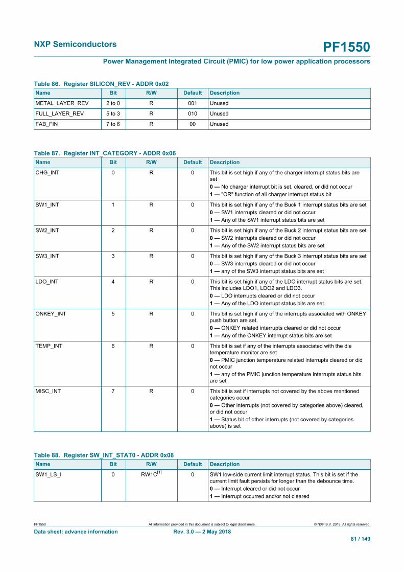
NXP Semiconductors PF1550Power Management Integrated Circuit (PMIC) for low power application processors
PF1550 All information provided in this document is subject to legal disclaimers. © NXP B.V. 2018. All rights reserved.
Data sheet: advance information Rev. 3.0 — 2 May 201881 / 149
Table 86. Register SILICON_REV - ADDR 0x02Name Bit R/W Default Description
METAL_LAYER_REV 2 to 0 R 001 Unused
FULL_LAYER_REV 5 to 3 R 010 Unused
FAB_FIN 7 to 6 R 00 Unused
Table 87. Register INT_CATEGORY - ADDR 0x06Name Bit R/W Default Description
CHG_INT 0 R 0 This bit is set high if any of the charger interrupt status bits areset0 — No charger interrupt bit is set, cleared, or did not occur1 — "OR" function of all charger interrupt status bit
SW1_INT 1 R 0 This bit is set high if any of the Buck 1 interrupt status bits are set0 — SW1 interrupts cleared or did not occur1 — Any of the SW1 interrupt status bits are set
SW2_INT 2 R 0 This bit is set high if any of the Buck 2 interrupt status bits are set0 — SW2 interrupts cleared or did not occur1 — Any of the SW2 interrupt status bits are set
SW3_INT 3 R 0 This bit is set high if any of the Buck 3 interrupt status bits are set0 — SW3 interrupts cleared or did not occur1 — any of the SW3 interrupt status bits are set
LDO_INT 4 R 0 This bit is set high if any of the LDO interrupt status bits are set.This includes LDO1, LDO2 and LDO3.0 — LDO interrupts cleared or did not occur1 — Any of the LDO interrupt status bits are set
ONKEY_INT 5 R 0 This bit is set high if any of the interrupts associated with ONKEYpush button are set.0 — ONKEY related interrupts cleared or did not occur1 — Any of the ONKEY interrupt status bits are set
TEMP_INT 6 R 0 This bit is set if any of the interrupts associated with the dietemperature monitor are set0 — PMIC junction temperature related interrupts cleared or didnot occur1 — any of the PMIC junction temperature interrupts status bitsare set
MISC_INT 7 R 0 This bit is set if interrupts not covered by the above mentionedcategories occur0 — Other interrupts (not covered by categories above) cleared,or did not occur1 — Status bit of other interrupts (not covered by categoriesabove) is set
Table 88. Register SW_INT_STAT0 - ADDR 0x08Name Bit R/W Default Description
SW1_LS_I 0 RW1C[1] 0 SW1 low-side current limit interrupt status. This bit is set if thecurrent limit fault persists for longer than the debounce time.0 — Interrupt cleared or did not occur1 — Interrupt occurred and/or not cleared

NXP Semiconductors PF1550Power Management Integrated Circuit (PMIC) for low power application processors
PF1550 All information provided in this document is subject to legal disclaimers. © NXP B.V. 2018. All rights reserved.
Data sheet: advance information Rev. 3.0 — 2 May 201882 / 149
Name Bit R/W Default Description
SW2_LS_I 1 RW1C 0 SW2 low-side current limit interrupt status. This bit is set if thecurrent limit fault persists for longer than the debounce time.0 — Interrupt cleared or did not occur1 — Interrupt occurred and/or not cleared
SW3_LS_I 2 RW1C 0 SW3 low-side current limit interrupt status. This bit is set if thecurrent limit fault persists for longer than the debounce time.0 — Interrupt cleared or did not occur1 — Interrupt occurred and/or not cleared
UNUSED 7 to 3 — — Unused
[1] Read or Write 1 to clear the bit
Table 89. Register SW_INT_MASK0 - ADDR 0x09Name Bit R/W Default Description
SW1_LS_M 0 RW 1 SW1 low-side current limit interrupt mask0 — Mask removed. INTB pin is pulled low if correspondinginterrupt status bit is set.1 — Mask enabled. INTB pin is NOT pulled low if correspondinginterrupt status bit is set.
SW2_LS_M 1 RW 1 SW2 low-side current limit interrupt mask0 — Mask removed. INTB pin is pulled low if correspondinginterrupt status bit is set.1 — Mask enabled. INTB pin is NOT pulled low if correspondinginterrupt status bit is set.
SW3_LS_M 2 RW 1 SW3 low-side current limit interrupt mask0 — Mask removed. INTB pin is pulled low if correspondinginterrupt status bit is set.1 — Mask enabled. INTB pin is NOT pulled low if correspondinginterrupt status bit is set.
UNUSED 7 to 3 — — Unused
Table 90. Register SW_INT_SENSE0 - ADDR 0x0AName Bit R/W Default Description
SW1_LS_S 0 R 0 SW1 low-side current limit interrupt sense. Sense is high as longas fault persists (post-debounce).0 — Fault removed1 — Fault exists
SW2_LS_S 1 R 0 SW2 low-side current limit interrupt sense. Sense is high as longas fault persists (post-debounce).0 — Fault removed1 — Fault exists
SW3_LS_S 2 R 0 SW3 low-side current limit interrupt sense. Sense is high as longas fault persists (post-debounce)0 — Fault removed1 — Fault exists
UNUSED 7 to 3 — — Unused
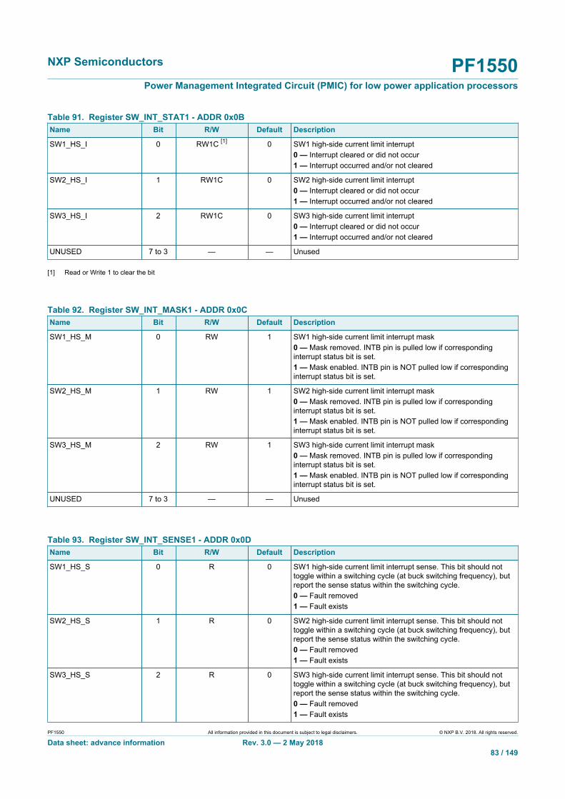
NXP Semiconductors PF1550Power Management Integrated Circuit (PMIC) for low power application processors
PF1550 All information provided in this document is subject to legal disclaimers. © NXP B.V. 2018. All rights reserved.
Data sheet: advance information Rev. 3.0 — 2 May 201883 / 149
Table 91. Register SW_INT_STAT1 - ADDR 0x0BName Bit R/W Default Description
SW1_HS_I 0 RW1C [1] 0 SW1 high-side current limit interrupt0 — Interrupt cleared or did not occur1 — Interrupt occurred and/or not cleared
SW2_HS_I 1 RW1C 0 SW2 high-side current limit interrupt0 — Interrupt cleared or did not occur1 — Interrupt occurred and/or not cleared
SW3_HS_I 2 RW1C 0 SW3 high-side current limit interrupt0 — Interrupt cleared or did not occur1 — Interrupt occurred and/or not cleared
UNUSED 7 to 3 — — Unused
[1] Read or Write 1 to clear the bit
Table 92. Register SW_INT_MASK1 - ADDR 0x0CName Bit R/W Default Description
SW1_HS_M 0 RW 1 SW1 high-side current limit interrupt mask0 — Mask removed. INTB pin is pulled low if correspondinginterrupt status bit is set.1 — Mask enabled. INTB pin is NOT pulled low if correspondinginterrupt status bit is set.
SW2_HS_M 1 RW 1 SW2 high-side current limit interrupt mask0 — Mask removed. INTB pin is pulled low if correspondinginterrupt status bit is set.1 — Mask enabled. INTB pin is NOT pulled low if correspondinginterrupt status bit is set.
SW3_HS_M 2 RW 1 SW3 high-side current limit interrupt mask0 — Mask removed. INTB pin is pulled low if correspondinginterrupt status bit is set.1 — Mask enabled. INTB pin is NOT pulled low if correspondinginterrupt status bit is set.
UNUSED 7 to 3 — — Unused
Table 93. Register SW_INT_SENSE1 - ADDR 0x0DName Bit R/W Default Description
SW1_HS_S 0 R 0 SW1 high-side current limit interrupt sense. This bit should nottoggle within a switching cycle (at buck switching frequency), butreport the sense status within the switching cycle.0 — Fault removed1 — Fault exists
SW2_HS_S 1 R 0 SW2 high-side current limit interrupt sense. This bit should nottoggle within a switching cycle (at buck switching frequency), butreport the sense status within the switching cycle.0 — Fault removed1 — Fault exists
SW3_HS_S 2 R 0 SW3 high-side current limit interrupt sense. This bit should nottoggle within a switching cycle (at buck switching frequency), butreport the sense status within the switching cycle.0 — Fault removed1 — Fault exists
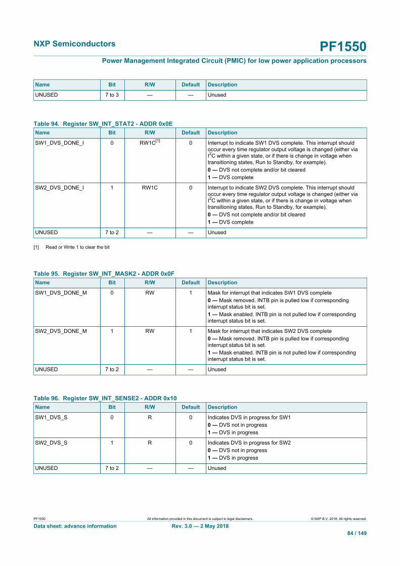
NXP Semiconductors PF1550Power Management Integrated Circuit (PMIC) for low power application processors
PF1550 All information provided in this document is subject to legal disclaimers. © NXP B.V. 2018. All rights reserved.
Data sheet: advance information Rev. 3.0 — 2 May 201884 / 149
Name Bit R/W Default Description
UNUSED 7 to 3 — — Unused
Table 94. Register SW_INT_STAT2 - ADDR 0x0EName Bit R/W Default Description
SW1_DVS_DONE_I 0 RW1C[1] 0 Interrupt to indicate SW1 DVS complete. This interrupt shouldoccur every time regulator output voltage is changed (either viaI2C within a given state, or if there is change in voltage whentransitioning states, Run to Standby, for example).0 — DVS not complete and/or bit cleared1 — DVS complete
SW2_DVS_DONE_I 1 RW1C 0 Interrupt to indicate SW2 DVS complete. This interrupt shouldoccur every time regulator output voltage is changed (either viaI2C within a given state, or if there is change in voltage whentransitioning states, Run to Standby, for example).0 — DVS not complete and/or bit cleared1 — DVS complete
UNUSED 7 to 2 — — Unused
[1] Read or Write 1 to clear the bit
Table 95. Register SW_INT_MASK2 - ADDR 0x0FName Bit R/W Default Description
SW1_DVS_DONE_M 0 RW 1 Mask for interrupt that indicates SW1 DVS complete0 — Mask removed. INTB pin is pulled low if correspondinginterrupt status bit is set.1 — Mask enabled. INTB pin is not pulled low if correspondinginterrupt status bit is set.
SW2_DVS_DONE_M 1 RW 1 Mask for interrupt that indicates SW2 DVS complete0 — Mask removed. INTB pin is pulled low if correspondinginterrupt status bit is set.1 — Mask enabled. INTB pin is not pulled low if correspondinginterrupt status bit is set.
UNUSED 7 to 2 — — Unused
Table 96. Register SW_INT_SENSE2 - ADDR 0x10Name Bit R/W Default Description
SW1_DVS_S 0 R 0 Indicates DVS in progress for SW10 — DVS not in progress1 — DVS in progress
SW2_DVS_S 1 R 0 Indicates DVS in progress for SW20 — DVS not in progress1 — DVS in progress
UNUSED 7 to 2 — — Unused

NXP Semiconductors PF1550Power Management Integrated Circuit (PMIC) for low power application processors
PF1550 All information provided in this document is subject to legal disclaimers. © NXP B.V. 2018. All rights reserved.
Data sheet: advance information Rev. 3.0 — 2 May 201885 / 149
Table 97. Register LDO_INT_STAT0 - ADDR 0x18Name Bit R/W Default Description
LDO1_FAULTI 0 RW1C[1] 0 LDO1 current limit interrupt0 — Interrupt cleared or did not occur1 — Interrupt occurred and/or not cleared
LDO2_FAULTI 1 RW1C 0 LDO2 current limit interrupt0 — Interrupt cleared or did not occur1 — Interrupt occurred and/or not cleared
LDO3_FAULTI 2 RW1C 0 LDO3 current limit interrupt0 — Interrupt cleared or did not occur1 — Interrupt occurred and/or not cleared
UNUSED 7 to 3 — — Unused
[1] Read or Write 1 to clear the bit
Table 98. Register LDO_INT_MASK0 - ADDR 0x19Name Bit R/W Default Description
LDO1_FAULTM 0 RW 1 LDO1 current limit fault interrupt mask0 — Mask removed. INTB pin is pulled low if correspondinginterrupt status bit is set.1 — Mask enabled. INTB pin is not pulled low if correspondinginterrupt status bit is set.
LDO2_FAULTM 1 RW 1 LDO2 current limit fault interrupt mask0 — Mask removed. INTB pin is pulled low if correspondinginterrupt status bit is set1 — Mask enabled. INTB pin is not pulled low if correspondinginterrupt status bit is set.
LDO3_FAULTM 2 RW 1 LDO3 current limit fault interrupt mask0 — Mask removed. INTB pin is pulled low if correspondinginterrupt status bit is set.1 — Mask enabled. INTB pin is not pulled low if correspondinginterrupt status bit is set.
UNUSED 7 to 3 — — Unused
Table 99. Register LDO_INT_SENSE0 - ADDR 0x1AName Bit R/W Default Description
LDO1_FAULTS 0 R 0 LDO1 fault interrupt sense0 — Fault removed1 — Fault exists
LDO2_FAULTS 1 R 0 LDO2 fault interrupt sense0 — Fault removed1 — Fault exists
LDO3_FAULTS 2 R 0 LDO3 fault interrupt sense0 — Fault removed1 — Fault exists
UNUSED 7 to 3 — — Unused

NXP Semiconductors PF1550Power Management Integrated Circuit (PMIC) for low power application processors
PF1550 All information provided in this document is subject to legal disclaimers. © NXP B.V. 2018. All rights reserved.
Data sheet: advance information Rev. 3.0 — 2 May 201886 / 149
Table 100. Register TEMP_INT_STAT0 - ADDR 0x20Name Bit R/W Default Description
THERM110I 0 RW1C[1] 0 Die temperature crosses 110 °C interrupt. Bidirectional interrupt.0 — Interrupt cleared or did not occur1 — Interrupt occurred and/or not cleared
UNUSED 1 — — Unused
THERM125I 2 RW1C 0 Die temperature crosses 125 °C interrupt. Bidirectional interrupt.0 — Interrupt cleared or did not occur1 — Interrupt occurred and/or not cleared
UNUSED 7 to 3 — — Unused
[1] Read or Write 1 to clear the bit
Table 101. Register TEMP_INT_MASK0 - ADDR 0x21Name Bit R/W Default Description
THERM110M 0 RW 1 Die temperature crosses 110 °C interrupt mask0 — Mask removed. INTB pin is pulled low if correspondinginterrupt status bit is set.1 — Mask enabled. INTB pin is NOT pulled low if correspondinginterrupt status bit is set.
UNUSED 1 — — Unused
THERM125M 2 RW 1 Die temperature crosses 125 °C interrupt mask0 — Mask removed. INTB pin is pulled low if correspondinginterrupt status bit is set.1 — Mask enabled. INTB pin is not pulled low if correspondinginterrupt status bit is set.
UNUSED 7 to 3 — — Unused
Table 102. Register TEMP_INT_SENSE0 - ADDR 0x22Name Bit R/W Default Description
THERM110S 0 R 0 110 °C interrupt sense0 — Die temperature below 110 °C1 — Die temperature above 110 °C
UNUSED 1 — — Unused
THERM125S 2 R 0 125 °C interrupt sense0 — Die temperature below 125 °C1 — Die temperature above 125 °C
UNUSED 7 to 3 — — Unused

NXP Semiconductors PF1550Power Management Integrated Circuit (PMIC) for low power application processors
PF1550 All information provided in this document is subject to legal disclaimers. © NXP B.V. 2018. All rights reserved.
Data sheet: advance information Rev. 3.0 — 2 May 201887 / 149
Table 103. Register ONKEY_INT_STAT0 - ADDR 0x24Name Bit R/W Default Description
ONKEY_PUSHI 0 RW1C [1] 0 Interrupt to indicate a push of the ONKEY button. Goes high afterdebounce.0 — Interrupt cleared or did not occur1 — Interrupt occurred and/or not cleared. Interrupt occurswhenever ONKEY button is pushed low for longer than the fallingedge debounce setting.Interrupt also occurs whenever ONKEY button is released highfor longer than the rising edge debounce setting, provided it wentpast the falling edge debounce time. In other words, this interruptoccurs whenever a change in status of the ONKEY_PUSHSsense bit occurs.
ONKEY_1SI 1 RW1C 0 Interrupt after ONKEY pressed for > 1 s0 — Interrupt cleared or did not occur1 — Interrupt occurred and/or not cleared
ONKEY_2SI 2 RW1C 0 Interrupt after ONKEY pressed for > 2 s0 — Interrupt cleared or did not occur1 — Interrupt occurred and/or not cleared
ONKEY_3SI 3 RW1C 0 Interrupt after ONKEY pressed for > 3 s0 — Interrupt cleared or did not occur1 — Interrupt occurred and/or not cleared
ONKEY_4SI 4 RW1C 0 Interrupt after ONKEY pressed for > 4 s0 — Interrupt cleared or did not occur1 — Interrupt occurred and/or not cleared
ONKEY_8SI 5 RW1C 0 Interrupt after ONKEY pressed for > 8 s0 — Interrupt cleared or did not occur1 — Interrupt occurred and/or not cleared
UNUSED 7 to 6 — — Unused
[1] Read or Write 1 to clear the bit
Table 104. Register ONKEY_INT_MASK0 - ADDR 0x25Name Bit R/W Default Description
ONKEY_PUSHM 0 RW 1 Interrupt mask for ONKEY_PUSH_I0 — Mask removed. INTB pin is pulled low if correspondinginterrupt status bit is set.1 — Mask enabled. INTB pin is not pulled low if correspondinginterrupt status bit is set.
ONKEY_1SM 1 RW 1 Interrupt mask for ONKEY_1SI0 — Mask removed. INTB pin is pulled low if correspondinginterrupt status bit is set.1 — Mask enabled. INTB pin is not pulled low if correspondinginterrupt status bit is set.
ONKEY_2SM 2 RW 1 Interrupt mask for ONKEY_2SI0 — Mask removed. INTB pin is pulled low if correspondinginterrupt status bit is set.1 — Mask enabled. INTB pin is NOT pulled low if correspondinginterrupt status bit is set.
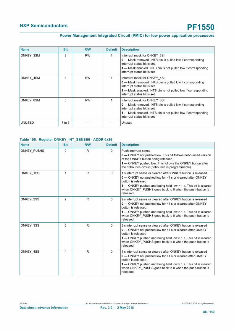
NXP Semiconductors PF1550Power Management Integrated Circuit (PMIC) for low power application processors
PF1550 All information provided in this document is subject to legal disclaimers. © NXP B.V. 2018. All rights reserved.
Data sheet: advance information Rev. 3.0 — 2 May 201888 / 149
Name Bit R/W Default Description
ONKEY_3SM 3 RW 1 Interrupt mask for ONKEY_3SI0 — Mask removed. INTB pin is pulled low if correspondinginterrupt status bit is set.1 — Mask enabled. INTB pin is not pulled low if correspondinginterrupt status bit is set.
ONKEY_4SM 4 RW 1 Interrupt mask for ONKEY_4SI0 — Mask removed. INTB pin is pulled low if correspondinginterrupt status bit is set.1 — Mask enabled. INTB pin is not pulled low if correspondinginterrupt status bit is set.
ONKEY_8SM 5 RW 1 Interrupt mask for ONKEY_8SI0 — Mask removed. INTB pin is pulled low if correspondinginterrupt status bit is set.1 — Mask enabled. INTB pin is not pulled low if correspondinginterrupt status bit is set.
UNUSED 7 to 6 — — Unused
Table 105. Register ONKEY_INT_SENSE0 - ADDR 0x26Name Bit R/W Default Description
ONKEY_PUSHS 0 R 0 Push interrupt sense0 — ONKEY not pushed low. This bit follows debounced versionof the ONKEY button being released.1 — ONKEY pushed low. This follows the ONKEY button afterthe debounce circuit (debounce is programmable).
ONKEY_1SS 1 R 0 1 s interrupt sense or cleared after ONKEY button is released0 — ONKEY not pushed low for >1 s or cleared after ONKEYbutton is released.1 — ONKEY pushed and being held low > 1 s. This bit is clearedwhen ONKEY_PUSHS goes back to 0 when the push-button isreleased.
ONKEY_2SS 2 R 0 2 s interrupt sense or cleared after ONKEY button is released0 — ONKEY not pushed low for >1 s or cleared after ONKEYbutton is released.1 — ONKEY pushed and being held low > 1 s. This bit is clearedwhen ONKEY_PUSHS goes back to 0 when the push-button isreleased.
ONKEY_3SS 3 R 0 3 s interrupt sense or cleared after ONKEY button is released0 — ONKEY not pushed low for >1 s or cleared after ONKEYbutton is released1 — ONKEY pushed and being held low > 1 s. This bit is clearedwhen ONKEY_PUSHS goes back to 0 when the push-button isreleased.
ONKEY_4SS 4 R 0 4 s interrupt sense or cleared after ONKEY button is released0 — ONKEY not pushed low for >1 s or cleared after ONKEYbutton is released.1 — ONKEY pushed and being held low > 1 s. This bit is clearedwhen ONKEY_PUSHS goes back to 0 when the push-button isreleased.

NXP Semiconductors PF1550Power Management Integrated Circuit (PMIC) for low power application processors
PF1550 All information provided in this document is subject to legal disclaimers. © NXP B.V. 2018. All rights reserved.
Data sheet: advance information Rev. 3.0 — 2 May 201889 / 149
Name Bit R/W Default Description
ONKEY_8SS 5 R 0 8 s interrupt sense or cleared after ONKEY button is released0 — ONKEY not pushed low for >1 s or cleared after ONKEYbutton is released.1 — ONKEY pushed and being held low > 1 s. This bit is clearedwhen ONKEY_PUSHS goes back to 0 when the push-button isreleased.
UNUSED 7 to 6 — — Unused
Table 106. Register MISC_INT_STAT0 - ADDR 0x28Name Bit R/W Default Description
PWRUP_I 0 RW1C[1] 0 Interrupt to indicate completion of transition from STANDBY toRUN and from SLEEP to RUN0 — Interrupt cleared or has not occurred1 — Interrupt has occurred
PWRDN_I 1 RW1C 0 Interrupt to indicate completion of transition from RUN toSTANDBY and from RUN to SLEEP0 — Interrupt cleared or has not occurred1 — Interrupt has occurred
PWRON_I 2 RW1C 0 Power on button event interrupt0 — Interrupt cleared or has not occurred1 — Interrupt has occurred
LOW_SYS_WARN_I 3 RW1C 0 LOW_SYS_WARN threshold crossed interrupt0 — Interrupt cleared or has not occurred1 — Interrupt has occurred
SYS_OVLO_I 4 RW1C 0 SYS_OVLO threshold crossed interrupt0 — Interrupt cleared or has not occurred1 — Interrupt has occurred
UNUSED 7 to 5 — — Unused
[1] Read or Write 1 to clear the bit
Table 107. Register MISC_INT_MASK0- ADDR 0x29Name Bit R/W Default Description
PWRUP_M 0 RW[1] 1 Mask for Interrupt to indicate completion on transition fromSTANDBY to RUN and from SLEEP to RUN0 — Mask removed. INTB pin is pulled low if correspondinginterrupt status bit is set.1 — Mask enabled. INTB pin is not pulled low if correspondinginterrupt status bit is set.
PWRDN_M 1 RW 1 Mask for Interrupt to indicate completion on transition from RUNto STANDBY and from RUN to SLEEP0 — Mask removed. INTB pin is pulled low if correspondinginterrupt status bit is set.1 — Mask enabled. INTB pin is not pulled low if correspondinginterrupt status bit is set.
PWRON_M 2 RW 1 Power on button event interrupt mask0 — Mask removed. INTB pin is pulled low if correspondinginterrupt status bit is set.1 — Mask enabled. INTB pin is not pulled low if correspondinginterrupt status bit is set.

NXP Semiconductors PF1550Power Management Integrated Circuit (PMIC) for low power application processors
PF1550 All information provided in this document is subject to legal disclaimers. © NXP B.V. 2018. All rights reserved.
Data sheet: advance information Rev. 3.0 — 2 May 201890 / 149
Name Bit R/W Default Description
LOW_SYS_WARN_M 3 RW 1 LOW_SYS_WARN threshold crossed interrupt mask0 — Mask removed. INTB pin is pulled low if correspondinginterrupt status bit is set.1 — Mask enabled. INTB pin is not pulled low if correspondinginterrupt status bit is set.
SYS_OVLO_M 4 RW 1 SYS_OVLO threshold crossed interrupt mask0 — Mask removed. INTB pin is pulled low if correspondinginterrupt status bit is set.1 — Mask enabled. INTB pin is not pulled low if correspondinginterrupt status bit is set.
UNUSED 7 to 5 — — Unused
[1] Asynchronous Set, Read and Write
Table 108. Register MISC_INT_SENSE0 - ADDR 0x2AName Bit R/W Default Description
PWRUP_S 0 R 0 Sense for interrupt to indicate completion on transition fromSTANDBY to RUN and from SLEEP to RUN0 — Transition not in progress1 — Transition in progress
PWRDN_S 1 R 0 Interrupt to indicate completion on transition from RUN toSTANDBY and from RUN to SLEEP0 — Transition not in progress1 — Transition in progress
PWRON_S 2 R 0 Power on button event interrupt sense0 — PWRON low1 — PWRON high
LOW_SYS_WARN_S 3 R 0 LOW_SYS_WARN threshold crossed interrupt sense0 — SYS > LOW_SYS_WARN1 — SYS < LOW_SYS_WARN
SYS_OVLO_S 4 R 0 SYS_OVLO threshold crossed interrupt sense0 — SYS < SYS_OVLO1 — SYS > SYS_OVLO
UNUSED 7 to 5 — — Unused
Table 109. Register COINCELL_CONTROL - ADDR 0x30Name Bit R/W Default Description
VCOIN 3 to 0 RW 0000 Coin cell charger charging voltage0000 — 1.8 V0111 — 3.3 V (goes up in 100 mV step per LSB)
COINCHEN 4 RW 0 Coin cell charger enable0 — Charger disabled1 — Charger enabled
UNUSED 7 to 5 — — Unused

NXP Semiconductors PF1550Power Management Integrated Circuit (PMIC) for low power application processors
PF1550 All information provided in this document is subject to legal disclaimers. © NXP B.V. 2018. All rights reserved.
Data sheet: advance information Rev. 3.0 — 2 May 201891 / 149
Table 110. Register SW1_VOLT - ADDR 0x32Name Bit R/W Default Description
SW1_VOLT 5 to 0 RW1S[1] — SW1 voltage setting register (Run mode)000000 — See Table 31 for voltage settings111111 — See Table 31 for voltage settingsReset condition — POR
UNUSED 7 to 5 — — Unused
[1] Load from OTP fuse, Read and Write
Table 111. Register SW1_STBY_VOLT - ADDR 0x33Name Bit R/W Default Description
SW1_STBY_VOLT 5 to 0 RW1S[1] — SW1 output voltage setting register (Standby mode). The defaultvalue here should be identical to SW1_VOLT[5:0] register.000000 — See Table 31 for voltage settings111111 — See Table 31 for voltage settings
UNUSED 7 to 6 — — Unused
[1] Load from OTP fuse, Read and Write
Table 112. Register SW1_SLP_VOLT - ADDR 0x34Name Bit R/W Default Description
SW1_SLP_VOLT 5 to 0 RW1S[1] — SW1 output voltage setting register (Sleep mode). The defaultvalue here should be identical to SW1_VOLT[5:0] register.000000 — See Table 31 for voltage settings111111 — See Table 31 for voltage settings
UNUSED 7 to 6 — — Unused
[1] Load from OTP fuse, Read and Write
Table 113. Register SW1_CTRL - ADDR 0x35Name Bit R/W Default Description
SW1_EN 0 RW1S[1] 0 Enables buck regulator. Loaded from OTP based on thesequence settings. User can turn regulator off by clearing this bit.0 — Regulator disabled in Run mode1 — Regulator enabled in Run mode
SW1_STBY_EN 1 RW1S 0 Enables buck regulator in Standby mode. User can turn regulatoroff by clearing this bit. The default value of this bit should beequal to the SW1_EN bit (based on OTP).0 — Regulator disabled in Standby mode1 — Regulator enabled in Standby mode
SW1_OMODE 2 RW[2] 0 Enables buck regulator in Sleep mode. User can turn regulator offby clearing this bit.0 — Regulator disabled in Sleep mode1 — Regulator enabled in Sleep mode

NXP Semiconductors PF1550Power Management Integrated Circuit (PMIC) for low power application processors
PF1550 All information provided in this document is subject to legal disclaimers. © NXP B.V. 2018. All rights reserved.
Data sheet: advance information Rev. 3.0 — 2 May 201892 / 149
Name Bit R/W Default Description
SW1_LPWR 3 RW 0 Enables the buck to enter Low-power mode during Standby andSleep0 — Regulator not in Low-power mode1 — Regulator in Low-power mode during Standby or Sleepmodes
SW1_DVSSPEED 4 RW1S 0 Controls slew rate of DVS transitions. Loaded from OTPand changeable by user after boot up. Not used whenOTP_SW1_DVS_SEL = 1.0 — DVS rate at 12.5 mV/2 μs1 — DVS rate at 12.5 mV/4 μs
SW1_FPWM_IN_DVS 5 RW 0 Enables CCM operation during DVS down0 — does not force FPWM during DVS1 — forces regulator to track the DVS reference while it is fallingrather than relying on the load current to pull the voltage low
SW1_FPWM 6 RW 0 Forces buck to go into CCM mode0 — Not in FPWM mode1 — Forced in PWM mode irrespective of load current
SW1_RDIS_ENB 7 RW1S 0 Controls discharge resistor on output when regulator disabled0 — Enables discharge resistor on output when regulatordisabled. Resistor connected at FB pin when regulator disabled toforce capacitor discharge.1 — Disables discharge resistor on output when regulatordisabled. Resistor not connected at FB pin when regulatordisabled. Relies on leakage/residue load to discharge outputcapacitor.
[1] Load from OTP fuse, Read and Write[2] Asynchronous Set, Read and Write
Table 114. Register SW1_SLP_VOLT - ADDR 0x36Name Bit R/W Default Description
SW1_ILIM 1 to 0 RW1S[1] 00 Sets current limit of SW1 regulator00 — Typical current limit of 1.0 A01 — Typical current limit of 1.2 A10 — Typical current limit of 1.5 A11 — Typical current limit of 2.0 A
UNUSED 3 to 2 — — Unused
SW1_TMODE_SEL 4 RW 0 0 — TON control1 — TOFF control
UNUSED 7 to 5 — — Unused
[1] Load from OTP fuse, Read and Write
Table 115. Register SW2_VOLT - ADDR 0x38Name Bit R/W Default Description
SW2_VOLT 5 to 0 RW1S[1] — SW2 voltage setting register (Run mode)000000 —See Table 31 for voltage settings111111 — See Table 31 for voltage settings
UNUSED 7 to 6 — — Unused

NXP Semiconductors PF1550Power Management Integrated Circuit (PMIC) for low power application processors
PF1550 All information provided in this document is subject to legal disclaimers. © NXP B.V. 2018. All rights reserved.
Data sheet: advance information Rev. 3.0 — 2 May 201893 / 149
[1] Load from OTP fuse, Read and Write
Table 116. Register SW2_STBY_VOLT - ADDR 0x39Name Bit R/W Default Description
SW2_STBY_VOLT 5 to 0 RW1S[1] — SW2 output voltage setting register (Standby mode). The defaultvalue here should be identical to SW2_VOLT[5:0] register.000000 — See Table 31 for voltage settings111111 — See Table 31 for voltage settings
UNUSED 7 to 6 — — Unused
[1] Load from OTP fuse, Read and Write
Table 117. Register SW2_SLP_VOLT - ADDR 0x3AName Bit R/W Default Description
SW2_SLP_VOLT 5 to 0 RW1S[1] — SW2 output voltage setting register (Sleep mode). The defaultvalue here should be identical to SW2_VOLT[5:0] register.000000 — See Table 31 for voltage settings111111 — See Table 31 for voltage settings
UNUSED 7 to 6 — — Unused
[1] Load from OTP fuse, Read and Write
Table 118. Register SW2_CTRL - ADDR 0x3BName Bit R/W Default Description
SW2_EN 0 RW1S[1] 0 Enables buck regulator. Loaded from OTP based on thesequence settings. User can turn regulator off by clearing this bit.0 — Regulator disabled in Run mode1 — Regulator enabled in Run mode
SW2_STBY_EN 1 RW1S 0 Enables buck regulator in Standby mode. User can turn regulatoroff by clearing this bit. The default value of this bit should beequal to the SW1_EN bit (based on OTP).0 — Regulator disabled in Standby mode1 — Regulator enabled in Standby mode
SW2_OMODE 2 RW 0 Enables buck regulator in Sleep mode. User can turn regulator offby clearing this bit.0 — Regulator disabled in Sleep mode1 — Regulator enabled in Sleep mode
SW2_LPWR 3 RW 0 Enables the buck to enter Low-power mode during Standby andSleep modes0 — Regulator not in Low-power mode1 — Regulator in Low-power mode during Standby or Sleep
SW2_DVSSPEED 4 RW1S 0 Controls slew rate of DVS transitions. Loaded from OTPand changeable by user after boot up. Not used whenOTP_SW2_DVS_SEL = 1.0 — DVS rate at 12.5 mV/2 μs1 — DVS rate at 12.5 mV/4 μs
SW2_FPWM_IN_DVS 5 RW 0 Enables CCM operation during DVS down0 — does not force FPWM during DVS1 — forces regulator to track the DVS reference while it is fallingrather than relying on the load current to pull the voltage low

NXP Semiconductors PF1550Power Management Integrated Circuit (PMIC) for low power application processors
PF1550 All information provided in this document is subject to legal disclaimers. © NXP B.V. 2018. All rights reserved.
Data sheet: advance information Rev. 3.0 — 2 May 201894 / 149
Name Bit R/W Default Description
SW2_FPWM 6 RW 0 Forces buck to go into CCM mode0 — Not in FPWM mode1 — Forced in PWM mode irrespective of load current.
SW2_RDIS_ENB 7 RW1S 0 Controls discharge resistor on output when regulator disabled0 — Enables discharge resistor on output when regulatordisabled. Resistor connected at FB pin when regulator disabled toforce capacitor discharge.1 — Disables discharge resistor on output when regulatordisabled. Resistor not connected at FB pin when regulatordisabled. Relies on leakage/residue load to discharge outputcapacitor.
[1] Load from OTP fuse, Read and Write
Table 119. Register SW2_CTRL1 - ADDR 0x3CName Bit R/W Default Description
SW2_ILIM 1 to 0 RW1S 00 Sets current limit of SW2 regulator00 — Typical current limit of 1.0 A01 — Typical current limit of 1.2 A10 — Typical current limit of 1.5 A11 — Typical current limit of 2.0 A
UNUSED 3 to 2 — — Unused
SW2_TMODE_SEL 4 RW 0 0 — TON control1 — TOFF control
UNUSED 7 to 5 — — Unused
Table 120. Register SW3_VOLT - ADDR 0x3EName Bit R/W Default Description
SW3_VOLT 3 to 0 RW1S — SW3 voltage setting register (Run mode). Loaded from fuses.Read only because DVS is not supported in this regulator.0000 — See Table 37 for voltage settings1111 — See Table 37 for voltage settings
UNUSED 7 to 4 — — Unused
Table 121. Register SW3_STBY_VOLT - ADDR 0x3FName Bit R/W Default Description
SW3_STBY_VOLT 3 to 0 RW1S — SW3 voltage setting register (Standby mode). Loaded from fuses.Read only because DVS is not supported in this regulator.0000 — See Table 37 for voltage settings1111 —See Table 37 for voltage settings
UNUSED 7 to 4 — — Unused
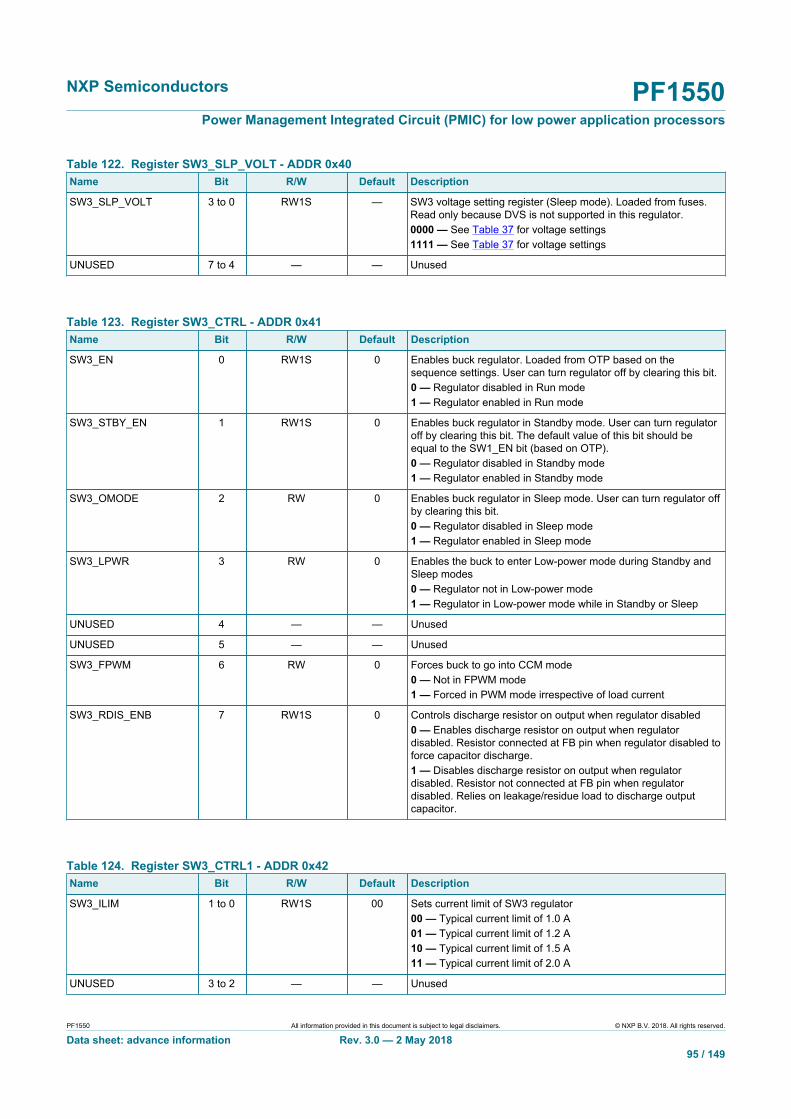
NXP Semiconductors PF1550Power Management Integrated Circuit (PMIC) for low power application processors
PF1550 All information provided in this document is subject to legal disclaimers. © NXP B.V. 2018. All rights reserved.
Data sheet: advance information Rev. 3.0 — 2 May 201895 / 149
Table 122. Register SW3_SLP_VOLT - ADDR 0x40Name Bit R/W Default Description
SW3_SLP_VOLT 3 to 0 RW1S — SW3 voltage setting register (Sleep mode). Loaded from fuses.Read only because DVS is not supported in this regulator.0000 — See Table 37 for voltage settings1111 — See Table 37 for voltage settings
UNUSED 7 to 4 — — Unused
Table 123. Register SW3_CTRL - ADDR 0x41Name Bit R/W Default Description
SW3_EN 0 RW1S 0 Enables buck regulator. Loaded from OTP based on thesequence settings. User can turn regulator off by clearing this bit.0 — Regulator disabled in Run mode1 — Regulator enabled in Run mode
SW3_STBY_EN 1 RW1S 0 Enables buck regulator in Standby mode. User can turn regulatoroff by clearing this bit. The default value of this bit should beequal to the SW1_EN bit (based on OTP).0 — Regulator disabled in Standby mode1 — Regulator enabled in Standby mode
SW3_OMODE 2 RW 0 Enables buck regulator in Sleep mode. User can turn regulator offby clearing this bit.0 — Regulator disabled in Sleep mode1 — Regulator enabled in Sleep mode
SW3_LPWR 3 RW 0 Enables the buck to enter Low-power mode during Standby andSleep modes0 — Regulator not in Low-power mode1 — Regulator in Low-power mode while in Standby or Sleep
UNUSED 4 — — Unused
UNUSED 5 — — Unused
SW3_FPWM 6 RW 0 Forces buck to go into CCM mode0 — Not in FPWM mode1 — Forced in PWM mode irrespective of load current
SW3_RDIS_ENB 7 RW1S 0 Controls discharge resistor on output when regulator disabled0 — Enables discharge resistor on output when regulatordisabled. Resistor connected at FB pin when regulator disabled toforce capacitor discharge.1 — Disables discharge resistor on output when regulatordisabled. Resistor not connected at FB pin when regulatordisabled. Relies on leakage/residue load to discharge outputcapacitor.
Table 124. Register SW3_CTRL1 - ADDR 0x42Name Bit R/W Default Description
SW3_ILIM 1 to 0 RW1S 00 Sets current limit of SW3 regulator00 — Typical current limit of 1.0 A01 — Typical current limit of 1.2 A10 — Typical current limit of 1.5 A11 — Typical current limit of 2.0 A
UNUSED 3 to 2 — — Unused

NXP Semiconductors PF1550Power Management Integrated Circuit (PMIC) for low power application processors
PF1550 All information provided in this document is subject to legal disclaimers. © NXP B.V. 2018. All rights reserved.
Data sheet: advance information Rev. 3.0 — 2 May 201896 / 149
Name Bit R/W Default Description
SW3_TMODE_SEL 4 RW 0 0 — TON control1 — TOFF control
UNUSED 7 to 5 — — Unused
Table 125. Register VSNVS_CTRL - ADDR 0x48Name Bit R/W Default Description
VSNVS_VOLT 2 to 0 RW1S 000 Not used in PF1550. Placeholder for future products.
CLKPULSE 3 RW 0 Optional bit used for evaluation. Refer to IP block
FORCEBOS 4 RW 0 Optional bit for evaluation0 — BOS circuit activated only when VSYS < UVDET1 — Forces best of supply circuit irrespective of UVDET
LIBGDIS 5 RW 0 Use to reduce quiescent current in coin cell mode0 — VSNVS local bandgap enabled in coin cell mode1 — VSNVS local bandgap disabled in coin cell mode to savequiescent current
UNUSED 7 to 6 — — Unused
Table 126. Register VREFDDR_CTRL - ADDR 0x4AName Bit R/W Default Description
VREFDDR_EN 0 RW1S 0 0 — Disables VREFDDR regulator1 — Enables VREFDDR regulator. This is set by the OTPsequence.
VREFDDR_STBY_EN 1 RW1S 0 The default value for this should be same as VREFDDREN0 — Disables VREFDDR regulator in Standby mode1 — Enables VREFDDR regulator in Standby mode ifVREFDDREN = 1
VREFDDR_OMODE 2 RW 0 0 — Keeps VREFDDR off in Off mode1 — Enables VREFDDR in Sleep mode if VREFDDREN = 1
VREFDDR_LPWR 3 RW 0 0 — Disables VREFDDR Low-power mode1 — Enables VREFDDR Low-power mode
UNUSED 7 to 4 — — Unused
Table 127. Register LDO1_VOLT - ADDR 0x4CName Bit R/W Default Description
LDO1_VOLT 4 to 0 RW1S — LDO1 output voltage setting register. Loaded from OTP.00000 — See Table 41 for voltage settings11111 — See Table 41 for voltage settings
UNUSED 7 to 5 — — Unused

NXP Semiconductors PF1550Power Management Integrated Circuit (PMIC) for low power application processors
PF1550 All information provided in this document is subject to legal disclaimers. © NXP B.V. 2018. All rights reserved.
Data sheet: advance information Rev. 3.0 — 2 May 201897 / 149
Table 128. Register LDO1_CTRL - ADDR 0x4DName Bit R/W Default Description
VLDO1_EN 0 RW1S 0 Enables LDO regulator. Loaded from OTP based on thesequence settings. User can turn regulator off by clearing this bit.0 — Disables regulator1 — Enables regulator
VLDO1_STBY_EN 1 RW1S 0 Enables LDO in Standby mode. Default value of this bit should besame as VLDO1_EN.0 — Disables regulator1 — Enables regulator
VLDO1_OMODE 2 RW 0 Enables LDO in Sleep mode0 — Disables regulator1 — Enables regulator
VLDO1_LPWR 3 RW 0 Forces LDO to Low-power mode in Sleep and Standby modes0 — Not in Low-power mode during Standby and Sleep1 — Regulator in Low-power mode during Standby and Sleep
LDO1_LS_EN 4 RW1S 0 This is loaded from OTP_LDOy_LS_EN and changeable from 0to 1 on power up. Changing from 1 to 0 is not allowed.0 — Sets LDOy in LDO mode1 — Sets LDOy to a load switch (fully on) mode
UNUSED 7 to 5 — — Unused
Table 129. Register LDO2_VOLT - ADDR 0x4FName Bit R/W Default Description
LDO2_VOLT 3 to 0 RW1S — LDO2 output voltage setting register. Loaded from OTP.0000 — See Table 43 for voltage settings1111 — See Table 43 for voltage settings
UNUSED 7 to 4 — — Unused
Table 130. Register LDO2_CTRL - ADDR 0x50Name Bit R/W Default Description
VLDO2_EN 0 RW1S 0 Enables LDO regulator. Loaded from OTP based on thesequence settings. User can turn regulator off by clearing this bit.0 — Disables regulator1 — Enables regulator
VLDO2_STBY_EN 1 RW1S 0 Enables LDO in Standby mode. Default value of this bit should besame as VLDO1_EN.0 — Disables regulator1 — Enables regulator
VLDO2_OMODE 2 RW 0 Enables LDO in Sleep mode0 — Disables regulator1 — Enables regulator
VLDO2_LPWR 3 RW 0 Forces LDO to Low-power mode in Sleep and Standby modes0 — Not in Low-power mode during Standby and Sleep1 — Regulator in Low-power mode during Standby and Sleep
UNUSED 7 to 4 — — Unused

NXP Semiconductors PF1550Power Management Integrated Circuit (PMIC) for low power application processors
PF1550 All information provided in this document is subject to legal disclaimers. © NXP B.V. 2018. All rights reserved.
Data sheet: advance information Rev. 3.0 — 2 May 201898 / 149
Table 131. Register LDO3_VOLT - ADDR 0x52Name Bit R/W Default Description
LDO3_VOLT 4 to 0 RW1S — LDO3 output voltage setting register. Loaded from OTP.00000 — See Table 41 for voltage settings11111 — See Table 41 for voltage settings
UNUSED 7 to 5 — — Unused
Table 132. Register LDO3_CTRL - ADDR 0x53Name Bit R/W Default Description
VLDO3_EN 0 RW1S 0 Enables LDO regulator. Loaded from OTP based on thesequence settings. User can turn regulator off by clearing this bit.0 — Disables regulator1 — Enables regulator
VLDO3_STBY_EN 1 RW1S 0 Enables LDO in Standby mode. Default value of this bit should besame as VLDO1_EN.0 — Disables regulator1 — Enables regulator
VLDO3_OMODE 2 RW 0 Enables LDO in Sleep mode0 — Disables regulator1 — Enables regulator
VLDO3_LPWR 3 RW 0 Forces LDO to Low-power mode in Sleep and Standby modes0 — Not in Low-power mode during Standby and Sleep1 — Regulator in Low-power mode during Standby and Sleep
LDO3_LS_EN 4 RW1S 0 This is loaded from OTP_LDOy_LS_EN and changeable from 0to 1 on power up. Changing from 1 to 0 is not allowed.0 — sets LDOy in LDO mode1 — sets LDOy to a load switch (fully on) mode
UNUSED 7 to 5 — — Unused
Table 133. Register PWRCTRL0 - ADDR 0x58Name Bit R/W Default Description
STANDBYDLY 1 to 0 RW 01 Controls delay of Standby pin after synchronization0 — No additional delay1 — 32 kHz cycle additional delay2 — 32 kHz cycle additional delay3 — 32 kHz cycle additional delay
STANDBYINV 2 RW 0 Controls polarity of STANDBY pin0 — Standby pin input active high1 — Standby pin input active low
POR_DLY 5 to 3 RW1S 000 Controls delay of RESETBMCU pin after power up (loaded fromOTP)000 — RESETBMCU goes high 2 ms after last regulator010 — RESETBMCU goes high 4 ms after last regulator011 — RESETBMCU goes high 8 ms after last regulator100 — RESETBMCU goes high 16 ms after last regulator101 — RESETBMCU goes high 128 ms after last regulator110 — RESETBMCU goes high 256 ms after last regulator111 — RESETBMCU goes high 1024 ms after last regulator
NXP Semiconductors PF1550Power Management Integrated Circuit (PMIC) for low power application processors
PF1550 All information provided in this document is subject to legal disclaimers. © NXP B.V. 2018. All rights reserved.
Data sheet: advance information Rev. 3.0 — 2 May 201899 / 149
Name Bit R/W Default Description
TGRESET 7 to 6 RW1S 00 Controls duration for which ONKEY has to be pushed low for aglobal reset (part goes to REGS_DISABLE)00 — 4 s01 — 8 s10 — 12 s11 — 16 s
Table 134. Register PWRCTRL1 - ADDR 0x59Name Bit R/W Default Description
PWRONDBNC 1 to 0 RW 00 Controls debounce of PWRON when in push-button mode(PWRON_CFG = 1)00 — 31.25 ms falling edge; 31.25 ms rising edge01 — 31.25 ms falling edge; 31.25 ms rising edge10 — 125 ms falling edge; 31.25 ms rising edge11 — 750 ms falling edge; 31.25 ms rising edge
ONKEYDBNC 3 to 2 RW 00 Controls debounce of ONKEY push button00 — 31.25 ms falling edge; 31.25 ms rising edge01 — 31.25 ms falling edge; 31.25 ms rising edge10 — 125 ms falling edge; 31.25 ms rising edge11 — 750 ms falling edge; 31.25 ms rising edge
PWRONRSTEN 4 RW 0 Enables going to REGS_DISABLE or Sleep mode whenPWRON_CFG = 1. See Section 10 "PF1550 state machine" fordetails.0 — Long press on PWRON button does not take state toREGS_DISABLE or Sleep1 — Long press on PWRON button takes state toREGS_DISABLE or Sleep
RESTARTEN 5 RW 0 Enables restart of system when PWRON push button is held lowfor 5 s0 — No impact1 — When going to REGS_DISABLE via a long press of PWRONbutton, holding it low for 1 more second takes state back to RUN(Equally, a 5 second push restarts the system)
REGSCPEN 6 RW 0 Shuts down LDO if it enters a current limit fault. Controls LDO1,LDO2 and LDO3.0 — LDO does not shut down in the event of a current limit fault.Continues to current limit1 — LDO is turned off when it encounters a current limit fault
ONKEY_RST_EN 7 RW 1 Enables turning off of system via ONKEY. See Section 10"PF1550 state machine" for details.0 — ONKEY cannot be used to turn off or restart system1 — ONKEY can be used to turn off or restart system
Table 135. Register PWRCTRL2 - ADDR 0x5AName Bit R/W Default Description
UVDET 1 to 0 RW1S 00 Sets UVDET threshold00 — Rising 2.65 V; Falling 2.55 V01 — Rising 2.8 V; Falling 2.7 V10 — Rising 3.0 V; Falling 2.9 V11 — Rising 3.1 V; Falling 3.0 V

NXP Semiconductors PF1550Power Management Integrated Circuit (PMIC) for low power application processors
PF1550 All information provided in this document is subject to legal disclaimers. © NXP B.V. 2018. All rights reserved.
Data sheet: advance information Rev. 3.0 — 2 May 2018100 / 149
Name Bit R/W Default Description
LOW_SYS_WARN 3 to 2 RW 00 Sets LOW_SYS_WARN threshold00 — Rising 3.3 V; Falling 3.1 V01 — Rising 3.5 V; Falling 3.3 V10 — Rising 3.7 V; Falling 3.5 V11 — Rising 3.9 V; Falling 3.7 V
UNUSED 7 to 4 — — Unused
Table 136. Register PWRCTRL3 - ADDR 0x5BName Bit R/W Default Description
GOTO_SHIP 0 RW 0 Set this bit to go to SHIP mode from any state. See Section 10"PF1550 state machine" for details.0 — No impact1 — PF1550 gracefully enters SHIP mode
GOTO_CORE_OFF 1 RW 0 Set this bit to go to CORE_OFF mode once in REGS_DISABLEstate0 — No impact1 — PF1550 gracefully enters CORE_OFF mode when inREGS_DISABLE state
UNUSED 7 to 2 — — Unused
Table 137. Register SW1_PWRDN_SEQ - ADDR 0x5FName Bit R/W Default Description
SW1_PWRDN_SEQ 2 to 0 RW1S 000 This contains same value as power-up sequence value bydefault. Power-up sequence is in mirror registers.xxx = The power-down sequencer performs the functionalopposite to the power-up sequencer. Each regulator hasan associated register setting (SW1_PWRDN_SEQ[2:0],SW2_PWRDN_SEQ[2:0], SW3_PWRDN_SEQ[2:0],LDO1_PWRDN_SEQ[2:0], LDO2_PWRDN_SEQ[2:0],LDO3_PWRDN_SEQ[2:0].VREFDDR_PWRDN_SEQ[2:0]) that sets its power-downsequence. The default setting of the above registers is equalto the corresponding power-up sequence setting. For example,SW1_PWRDN_SEQ[2:0] = OTP_SW1_PWRUP_SEQ[2:0].When the power-down sequencer is activated, regulatorsare turned off one by one in the descending order of theXXX_PWRDN_SEQ[2:0] setting. This way, by default, power-down is a mirror of the power-up sequence. In one of the"System On" states, the processor can change the values of theXXX_PWRDN_SEQ[2:0] registers. The power-up sequence isfixed by OTP (or TBB). If all XXX_PWRDN_SEQ[2:0] = 0x00, thepower-down sequencer is bypassed and all the regulators areturned off at once.
UNUSED 7 to 3 — — Unused

NXP Semiconductors PF1550Power Management Integrated Circuit (PMIC) for low power application processors
PF1550 All information provided in this document is subject to legal disclaimers. © NXP B.V. 2018. All rights reserved.
Data sheet: advance information Rev. 3.0 — 2 May 2018101 / 149
Table 138. Register SW2_PWRDN_SEQ - ADDR 0x60Name Bit R/W Default Description
SW2_PWRDN_SEQ 2 to 0 RW1S 000 This contains same value as power-up sequence value bydefault. Power-up sequence is in mirror registers.xxx = The power-down sequencer performs the functionalopposite to the power-up sequencer. Each regulator hasan associated register setting (SW1_PWRDN_SEQ[2:0],SW2_PWRDN_SEQ[2:0], SW3_PWRDN_SEQ[2:0],LDO1_PWRDN_SEQ[2:0], LDO2_PWRDN_SEQ[2:0],LDO3_PWRDN_SEQ[2:0].VREFDDR_PWRDN_SEQ[2:0]) that sets its power-downsequence. The default setting of the above registers is equalto the corresponding power-up sequence setting. For example,SW1_PWRDN_SEQ[2:0] = OTP_SW1_PWRUP_SEQ[2:0].When the power-down sequencer is activated, regulatorsare turned off one by one in the descending order of theXXX_PWRDN_SEQ[2:0] setting. This way, by default, power-down is a mirror of the power-up sequence. In one of the"System On" states, the processor can change the values of theXXX_PWRDN_SEQ[2:0] registers. The power-up sequence isfixed by OTP (or TBB). If all XXX_PWRDN_SEQ[2:0] = 0x00, thepower-down sequencer is bypassed and all the regulators areturned off at once.
UNUSED 7 to 3 — — Unused
Table 139. Register SW2_PWRDN_SEQ - ADDR 0x61Name Bit R/W Default Description
SW3_PWRDN_SEQ 2 to 0 RW1S 000 This contains same value as power-up sequence value bydefault. Power-up sequence is in mirror registers.xxx = The power-down sequencer performs the functionalopposite to the power-up sequencer. Each regulator hasan associated register setting (SW1_PWRDN_SEQ[2:0],SW2_PWRDN_SEQ[2:0], SW3_PWRDN_SEQ[2:0],LDO1_PWRDN_SEQ[2:0], LDO2_PWRDN_SEQ[2:0],LDO3_PWRDN_SEQ[2:0].VREFDDR_PWRDN_SEQ[2:0]) that sets its power-downsequence. The default setting of the above registers is equalto the corresponding power-up sequence setting. For example,SW1_PWRDN_SEQ[2:0] = OTP_SW1_PWRUP_SEQ[2:0].When the power-down sequencer is activated, regulatorsare turned off one by one in the descending order of theXXX_PWRDN_SEQ[2:0] setting. This way, by default, power-down is a mirror of the power-up sequence. In one of the"System On" states, the processor can change the values of theXXX_PWRDN_SEQ[2:0] registers. The power-up sequence isfixed by OTP (or TBB). If all XXX_PWRDN_SEQ[2:0] = 0x00, thepower-down sequencer is bypassed and all the regulators areturned off at once.
UNUSED 7 to 3 — — Unused

NXP Semiconductors PF1550Power Management Integrated Circuit (PMIC) for low power application processors
PF1550 All information provided in this document is subject to legal disclaimers. © NXP B.V. 2018. All rights reserved.
Data sheet: advance information Rev. 3.0 — 2 May 2018102 / 149
Table 140. Register LDO1_PWRDN_SEQ - ADDR 0x62Name Bit R/W Default Description
LDO1_PWRDN_SEQ 2 to 0 RW1S 000 This contains same value as power-up sequence value bydefault. Power-up sequence is in mirror registers.xxx = The power-down sequencer performs the functionalopposite to the power-up sequencer. Each regulator hasan associated register setting (SW1_PWRDN_SEQ[2:0],SW2_PWRDN_SEQ[2:0], SW3_PWRDN_SEQ[2:0],LDO1_PWRDN_SEQ[2:0], LDO2_PWRDN_SEQ[2:0],LDO3_PWRDN_SEQ[2:0].VREFDDR_PWRDN_SEQ[2:0]) that sets its power-downsequence. The default setting of the above registers is equalto the corresponding power-up sequence setting. For example,SW1_PWRDN_SEQ[2:0] = OTP_SW1_PWRUP_SEQ[2:0].When the power-down sequencer is activated, regulatorsare turned off one by one in the descending order of theXXX_PWRDN_SEQ[2:0] setting. This way, by default, power-down is a mirror of the power-up sequence. In one of the"System On" states, the processor can change the values of theXXX_PWRDN_SEQ[2:0] registers. The power-up sequence isfixed by OTP (or TBB). If all XXX_PWRDN_SEQ[2:0] = 0x00, thepower-down sequencer is bypassed and all the regulators areturned off at once.
UNUSED 7 to 3 — — Unused
Table 141. Register LDO2_PWRDN_SEQ - ADDR 0x63Name Bit R/W Default Description
LDO2_PWRDN_SEQ 2 to 0 RW1S 000 This contains same value as power-up sequence value bydefault. Power-up sequence is in mirror registers.xxx = The power-down sequencer performs the functionalopposite to the power-up sequencer. Each regulator hasan associated register setting (SW1_PWRDN_SEQ[2:0],SW2_PWRDN_SEQ[2:0], SW3_PWRDN_SEQ[2:0],LDO1_PWRDN_SEQ[2:0], LDO2_PWRDN_SEQ[2:0],LDO3_PWRDN_SEQ[2:0].VREFDDR_PWRDN_SEQ[2:0]) that sets its power-downsequence. The default setting of the above registers is equalto the corresponding power-up sequence setting. For example,SW1_PWRDN_SEQ[2:0] = OTP_SW1_PWRUP_SEQ[2:0].When the power-down sequencer is activated, regulatorsare turned off one by one in the descending order of theXXX_PWRDN_SEQ[2:0] setting. This way, by default, power-down is a mirror of the power-up sequence. In one of the"System On" states, the processor can change the values of theXXX_PWRDN_SEQ[2:0] registers. The power-up sequence isfixed by OTP (or TBB). If all XXX_PWRDN_SEQ[2:0] = 0x00, thepower-down sequencer is bypassed and all the regulators areturned off at once.
UNUSED 7 to 3 — — Unused

NXP Semiconductors PF1550Power Management Integrated Circuit (PMIC) for low power application processors
PF1550 All information provided in this document is subject to legal disclaimers. © NXP B.V. 2018. All rights reserved.
Data sheet: advance information Rev. 3.0 — 2 May 2018103 / 149
Table 142. Register LDO3_PWRDN_SEQ - ADDR 0x64Name Bit R/W Default Description
LDO3_PWRDN_SEQ 2 to 0 RW1S 000 This contains same value as power-up sequence value bydefault. Power-up sequence is in mirror registers.xxx = The power-down sequencer performs the functionalopposite to the power-up sequencer. Each regulator hasan associated register setting (SW1_PWRDN_SEQ[2:0],SW2_PWRDN_SEQ[2:0], SW3_PWRDN_SEQ[2:0],LDO1_PWRDN_SEQ[2:0], LDO2_PWRDN_SEQ[2:0],LDO3_PWRDN_SEQ[2:0].VREFDDR_PWRDN_SEQ[2:0]) that sets its power-downsequence. The default setting of the above registers is equalto the corresponding power-up sequence setting. For example,SW1_PWRDN_SEQ[2:0] = OTP_SW1_PWRUP_SEQ[2:0].When the power-down sequencer is activated, regulatorsare turned off one by one in the descending order of theXXX_PWRDN_SEQ[2:0] setting. This way, by default, power-down is a mirror of the power-up sequence. In one of the"System On" states, the processor can change the values of theXXX_PWRDN_SEQ[2:0] registers. The power-up sequence isfixed by OTP (or TBB). If all XXX_PWRDN_SEQ[2:0] = 0x00, thepower-down sequencer is bypassed and all the regulators areturned off at once.
UNUSED 7 to 3 — — Unused
Table 143. Register VREFDDR_PWRDN_SEQ - ADDR 0x65Name Bit R/W Default Description
VREFDDR_PWRDN_SEQ
2 to 0 RW1S 000 This contains same value as power-up sequence value bydefault. Power-up sequence is in mirror registers.xxx = The power-down sequencer performs the functionalopposite to the power-up sequencer. Each regulator hasan associated register setting (SW1_PWRDN_SEQ[2:0],SW2_PWRDN_SEQ[2:0], SW3_PWRDN_SEQ[2:0],LDO1_PWRDN_SEQ[2:0], LDO2_PWRDN_SEQ[2:0],LDO3_PWRDN_SEQ[2:0].VREFDDR_PWRDN_SEQ[2:0]) that sets its power-downsequence. The default setting of the above registers is equalto the corresponding power-up sequence setting. For example,SW1_PWRDN_SEQ[2:0] = OTP_SW1_PWRUP_SEQ[2:0].When the power-down sequencer is activated, regulatorsare turned off one by one in the descending order of theXXX_PWRDN_SEQ[2:0] setting. This way, by default, power-down is a mirror of the power-up sequence. In one of the"System On" states, the processor can change the values of theXXX_PWRDN_SEQ[2:0] registers. The power-up sequence isfixed by OTP (or TBB). If all XXX_PWRDN_SEQ[2:0] = 0x00, thepower-down sequencer is bypassed and all the regulators areturned off at once.
UNUSED 7 to 3 — — Unused

NXP Semiconductors PF1550Power Management Integrated Circuit (PMIC) for low power application processors
PF1550 All information provided in this document is subject to legal disclaimers. © NXP B.V. 2018. All rights reserved.
Data sheet: advance information Rev. 3.0 — 2 May 2018104 / 149
Table 144. Register STATE_INFO - ADDR 0x67Name Bit R/W Default Description
STATE 5 to 0 R 000000 Indicates machine state000000 — Wait status001100 — RUN state001101 — STANDBY state001110 — SLEEP/LPSR state101011 — REGS_DISABLE stateOther bits are reserved
UNUSED 7 to 6 — — Unused
Table 145. Register I2C_ADDR - ADDR 0x68Name Bit R/W Default Description
I2C_SLAVE_ADDR_LSBS
2 to 0 R 000 Loaded from fuses. But read only in functional space.000 — Slave Address: 0x08001 — Slave Address: 0x09010 — Slave Address: 0x0A011 — Slave Address: 0x0B100 — Slave Address: 0x0C101 — Slave Address: 0x0D110 — Slave Address: 0x0E111 — Slave Address: 0x0F
USE_DEFAULT_ADD R 7 RW 0 DEFAULT ADDR
Table 146. Register RC_16MHZ - ADDR 0x6BName Bit R/W Default Description
REQ_16MHZ 0 RW 0 Enables 16 MHz clock0 — 16 MHz clock enable controlled by state machine1 — 16 MHz clock always enabled
REQ_ACORE_ON 1 RW 0 Controls Analog core enable0 — Analog core enable controlled by state machine1 — Analog core always on
REQ_ACORE_HIPWR 2 RW 0 Controls Low-power mode of the analog core0 — Analog core Low-power mode controlled by state machine1 — Analog core never in Low-power mode
UNUSED 7 to 3 — — Unused
Table 147. Register KEY1 - ADDR 0x6BName Bit R/W Default Description
KEY1 7 to 0 RW 0x00 Unused

NXP Semiconductors PF1550Power Management Integrated Circuit (PMIC) for low power application processors
PF1550 All information provided in this document is subject to legal disclaimers. © NXP B.V. 2018. All rights reserved.
Data sheet: advance information Rev. 3.0 — 2 May 2018105 / 149
12.2 Specific Charger Registers (Offset is 0x80)
Table 148. Register CHG_INT - ADDR 0x00Name Bit R/W Default Description
SUP_I 0 RW1S[1] 0 Supplement mode interrupt0 — The SUP_OK bit interrupt has not occurred or been cleared1 — The SUP_OK bit interrupt has occurredReset condition — VCOREDIG_RSTB
BAT2SOC_I 1 RW1S 0 VBATT to VSYS overcurrent interrupt0 — The BAT2SOC_OK interrupt has not occurred or beencleared1— The BAT2SOC _OK bit interrupt has occurredReset condition — VCOREDIG_RSTB
BAT_I 2 RW1S 0 Battery interrupt0 — The BAT_OK interrupt has not occurred or been cleared1 — The BAT_OK interrupt has occurredReset condition — VCOREDIG_RSTB
CHG_I 3 RW1S 0 Charger interrupt0 — The CHG_OK interrupt has not occurred or been cleared1 — The CHG_OK interrupt has occurredReset condition — VCOREDIG_RSTB
RSVD4 4 RW1S 0 Unused
VBUS_I 5 RW1S 0 VBUS interrupt0 — The VBUS_OK interrupt has not occurred or been cleared1 — The VBUS_OK interrupt has occurredReset condition — VCOREDIG_RSTB
VBUS_DPM_I 6 RW1S 0 VBUS_DPM interrupt0 — The VBUS_DPM _OK interrupt has not occurred or beencleared1 — The VBUS_DPM _OK interrupt has occurredReset condition — VCOREDIG_RSTB
THM_I 7 RW1S 0 THM interrupt. Occurs when Warm/Cool thresholds are crossedor when thermal foldback is active. After the interrupt hasoccurred, THM_OK bit can be read to know the source of theinterrupt.If THM_OK = 0, warm/cool thresholds are crossedIf THM_OK = 1, thermal foldback is active0 — THM interrupt has not occurred or has been cleared1 — THM interrupt has occurredReset condition — VCOREDIG_RSTB
[1] Load from OTP fuse, Read and Write
Table 149. Register CHG_INT_MASK - ADDR 0x02Name Bit R/W Default Description
SUP_M 0 RW 1 Supplement mode interrupt mask0 — Unmasked1 — MaskedReset condition — VCOREDIG_RSTB

NXP Semiconductors PF1550Power Management Integrated Circuit (PMIC) for low power application processors
PF1550 All information provided in this document is subject to legal disclaimers. © NXP B.V. 2018. All rights reserved.
Data sheet: advance information Rev. 3.0 — 2 May 2018106 / 149
Name Bit R/W Default Description
BAT2SOC_M 1 RW 1 VBATT to VSYS overcurrent interrupt mask0 — Unmasked1 — MaskedReset condition — VCOREDIG_RSTB
BAT_M 2 RW 1 Battery interrupt mask0 — Unmasked1 — MaskedReset condition — VCOREDIG_RSTB
CHG_M 3 RW 1 Charger interrupt mask0 — Unmasked1 — MaskedReset condition — VCOREDIG_RSTB
RSVD4 4 RW 1 Unused
VBUS_M 5 RW 1 VBUS interrupt mask0 — Unmasked1 — MaskedReset condition — VCOREDIG_RSTB
VBUS_DPM_M 6 RW 1 VBUS_DPM interrupt mask0 — Unmasked1 — MaskedReset condition — VCOREDIG_RSTB
THM_M 7 RW 1 THM interrupt mask0 — Unmasked1 — MaskedReset condition — VCOREDIG_RSTB
Table 150. Register CHG_INT_OK - ADDR 0x04Name Bit R/W Default Description
SUP_OK 0 R 0 Supplement mode indicator0 — Supplement mode not detected1 — Supplement mode detectedReset condition — VCOREDIG_RSTB
BAT2SOC_OK 1 R 0 Single-bit battery overcurrent indicator0 — Battery to VSYS has not hit overcurrent limit1 — Battery to VSYS has hit overcurrent limit (BATT_SNS Bit 5 =0b1)Reset condition — VCOREDIG_RSTB
BAT_OK 2 R 1 Single-bit battery status indicator. See BATT_SNS for moreinformation.0 — The battery has an issue or the charger has beensuspended, for example, BAT_SNS = 0x06 or 0x07 or 0x091 — The battery is okay, for example, BAT_SNS ≠ 0x06 or 0x07or 0x09Reset condition — VCOREDIG_RSTB

NXP Semiconductors PF1550Power Management Integrated Circuit (PMIC) for low power application processors
PF1550 All information provided in this document is subject to legal disclaimers. © NXP B.V. 2018. All rights reserved.
Data sheet: advance information Rev. 3.0 — 2 May 2018107 / 149
Name Bit R/W Default Description
CHG_OK 3 R 0 Single-bit charger status indicator. See CHG_SNS for moreinformation.Reset condition — VCOREDIG_RSTB0 — The charger is not charging, has suspended charging orThermal Reg = 1, for example, CHG_SNS ≠ 0x00 or 0x01 or 0x02or 0x031 — The charger is okay, for example, CHG_SNS = 0x00 or 0x01or 0x02 or 0x03Reset condition — VCOREDIG_RSTB
RSVD4 4 R 0 Unused
VBUS_OK 5 R 0 Single-bit VBUS_LIN input status indicator. See VBUS_LIN_SNSfor more information.0 — The VBUS_LIN input is invalid. For example, VBUS_VALID= 0.1 — The VBUS_LIN input is valid. For example, VBUS_VALID =1.Reset condition — VCOREDIG_RSTB
VBUS_DPM_OK 6 R 0 VBUS_DPM status indicator. This register provides status of inputDynamic Power Management threshold.0 — Not in VBUS_DPM mode1 — VBUS_DPM modeReset condition — VCOREDIG_RSTB
THM_OK 7 R 1 Thermistor status indicator. This register provides information onwhether battery temperature is within or outside the thermistorcool/warm thresholds.0 — Thermistor outside cool and warm thresholds1 — Thermistor between cool and warm thresholdsReset condition — VCOREDIG_RSTB
Table 151. Register VBUS_SNS - ADDR 0x06Name Bit R/W Default Description
RSVD0 1 to 0 R 00 Unused
VBUS_UVLO_SNS 2 R 1 0 — VBUS_ LIN > VBUS_LIN_UVLO1 — VBUS_ LIN < VBUS_LIN_UVLO or when VBUS is detached
VBUS_IN2SYS_SNS 3 R 1 0 — VBUS_ LIN > VBATT + VIN2SYS1 — VBUS_ LIN < VBATT + VIN2SYS
VBUS_OVLO_SNS 4 R 0 0 — VBUS_ LIN < VBUS_LIN_OVLO1 — VBUS_ LIN > VBUS_LIN_OVLO
VBUS_VALID 5 R 0 0 — VBUS is not valid1 — VBUS is valid, VBUS_LIN > VBUS_LIN_UVLO, VBUS_LIN >VBATT + VIN2SYS, VBUS_LIN < VBUS_LIN_OVLOReset condition — VCOREDIG_RSTB
RSVD6 6 R 0 Unused
VBUS_DPM_SNS 7 R 0 VBUS_LIN DPM sense details0 — VBUS _LIN DPM threshold has not been triggered1 — VBUS_LIN DPM threshold has been triggered
NXP Semiconductors PF1550Power Management Integrated Circuit (PMIC) for low power application processors
PF1550 All information provided in this document is subject to legal disclaimers. © NXP B.V. 2018. All rights reserved.
Data sheet: advance information Rev. 3.0 — 2 May 2018108 / 149
Table 152. Register CHG_SNS - ADDR 0x07Name Bit R/W Default Description
CHG_SNS 3 to 0 R 1000 Charger sense0 — Charger is in precharge mode, CHG_OK = 1, VBATT <VPRECHG.LB, TJ < TSHDN1 — Charger is in fast-charge constant current mode, CHG_OK =1, VBATT < VBATREG, TJ < TSHDN2 — Charger is in fast-charge constant voltage mode, CHG_OK =1, VBATT = VBATREG, TJ < TSHDN3 — Charger is in end-of-charge mode, CHG_OK = 1, VBATT ≥VBATREG, IBAT = IEOC, TJ < TSHDN4 — Charger is in done mode, CHG_OK = 0, VBATT >VBATREG-VRESTART, TJ < TSHDN5 — Reserved6 — Charger is in timer fault mode, CHG_OK = 0, VBATT <VBATOV, if BAT_SNS = 0b001 then VBATT < VBATPC, TJ <TSHDN7 — Charger is in thermistor suspend mode, CHG_OK =0, VBATT < VBATOV, if BAT_SNS = 0b001 then VBATT <VPRECHG.LB, TJ < TSHDN8 — Charger is off, input invalid and/or charger is disabled,CHG_OK = 09 — Battery overvoltage condition10 — Charger is off and TJ > TSHDN, CHG_OK = 0000011 — Reserved12 — Charger block is in Linear only mode, not charging,CHG_OK = 013 — Reserved14 — Reserved15 — ReservedReset condition — VCOREDIG_RSTB
RSVD4 4 R 0 Unused
WDT_SNS 5 R 0 Watchdog sense bit0 — Watchdog timer has not expired1 — Charger is off because the watchdog timer expired,CHG_OK = 0Reset condition — VCOREDIG_RSTB
THM_SNS 6 R 0 Cool/Warm sense bit0 — Thermistor temperature is between cool and warmthresholds1 — Thermistor temperature is < Cool, or > Warm thresholdReset condition — VCOREDIG_RSTB
TREG_SNS 7 R 0 Temperature regulation sense0 — The junction temperature is less than the threshold set byREGTEMP and the full charge current limit is available1 — The junction temperature is greater than the threshold set byREGTEMP and the charge current limit may be folding back toreduce power dissipationReset condition — VCOREDIG_RSTB

NXP Semiconductors PF1550Power Management Integrated Circuit (PMIC) for low power application processors
PF1550 All information provided in this document is subject to legal disclaimers. © NXP B.V. 2018. All rights reserved.
Data sheet: advance information Rev. 3.0 — 2 May 2018109 / 149
Table 153. Register BATT_SNS - ADDR 0x08Name Bit R/W Default Description
BATT_SNS 2 to 0 R 000 0 — 0x00 = No valid VBUS input1 — 0x01 = VBATT < VPRECHG.LB2 — 0x02 = the battery cannot charge beyond the prechargethreshold and charging has suspended and is in timer fault mode.This condition is also reported in the CHG_SNS as 0x06.3 — Reserved4 — 0x04 = VPRECHG.LB < VBATT5 — 0x05 = the battery voltage is greater than the batteryovervoltage flag threshold (VBATOV). Note that this flag is only begenerated when there is a valid input.6 — 0x06 = battery not detected with a valid input and aftersystem wake-up7 — ReservedReset condition — VCOREDIG_RSTB
RSVD3 4 to 3 RW 00 Unused
BATTOC_SNS 5 R 0 VBATT to VSYS overcurrent fault0 — No fault1 — VBATT to VSYS in high current faultReset condition — VCOREDIG_RSTB
RSVD6 7 to 6 RW 00 Unused
Table 154. Register CHG_OPER- ADDR 0x09Name Bit R/W Default Description
CHG_OPER 1 to 0 RW1S[1] 01 Charger operation configuration0 — charger = off, linear = off. The BATFET switch is on to allowthe battery to support the system.1 — charger = off, linear = on. When there is a valid VBUS inputand no battery, the linear regulator regulates the VSYS voltage toVSYSMIN[1:0].2 — charger = on, linear = on. When there is a valid input, thebattery is charging. VSYS is the larger of VSYSMIN and VBATT +IBAT * RBATFET.3 — ReservedReset condition — VCOREDIG_RSTB
UNUSED 2 RW 0 Unused
WDTEN 3 RW 0 Enable watchdog timer bit. While enabled, the system controllermust reset the watchdog timer within the timer period (tWD) forthe charger to operate normally. Reset the watchdog timer byprogramming WDTCLR = 0x01.0 — Watchdog timer disabled1 — Watchdog timer enabledReset condition — VCOREDIG_RSTB
DISBATFET 4 RW 0 VBATT to VSYS FET disable control0 — VBATT to VSYS FET is controlled by internal state machine1 — VBATT to VSYS FET is forced offReset condition — VCOREDIG_RSTB
UNUSED 7 to 5 RW 000 Unused
[1] Load from OTP fuse, Read and Write

NXP Semiconductors PF1550Power Management Integrated Circuit (PMIC) for low power application processors
PF1550 All information provided in this document is subject to legal disclaimers. © NXP B.V. 2018. All rights reserved.
Data sheet: advance information Rev. 3.0 — 2 May 2018110 / 149
Table 155. Register CHG_TMR - ADDR 0x0AName Bit R/W Default Description
FCHGTIME 2 to 0 RW1S 010 Fast-charge timer duration (tFC)0 — Disable1 — 2 hrs2 — 4 hrs3 — 6 hrs4 — 8 hrs5 — 10 hrs6 — 12 hrs7 — 14 hrsReset condition — VCOREDIG_RSTB
EOCTIME 5 to 3 RW1S 001 End-of-charge timer setting0 — 0 min (16 secs debounce)1 — 10 min2 — 20 min3 — 30 min4 — 40 min5 — 50 min6 — 60 min7 — 70 minReset condition — VCOREDIG_RSTB
RSVD6 6 R 0 Unused
TPRECHG 7 RW1S 0 Precharge timer value. Used for low battery.0 — Precharge timer value = 30 min1 — Precharge timer value = 45 minReset condition — VCOREDIG_RSTB
Table 156. Register CHG_EOC_CNFG - ADDR 0x0DName Bit R/W Default Description
CHG_RESTART 1 to 0 RW1S 01 Charger restart threshold00 — 0x00 = 100 mV below the value programmed byCHG_CV_PRM01 — 0x01 = 150 mV below the value programmed byCHG_CV_PRM02 — 0x02 = 200 mV below the value programmed byCHG_CV_PRM03 — 0x03 = disabledReset condition — VCOREDIG_RSTB
FORCE_BATT_ISO 2 RW1S 0 Unused
EOC_EXIT 3 RW1S 0 Unused

NXP Semiconductors PF1550Power Management Integrated Circuit (PMIC) for low power application processors
PF1550 All information provided in this document is subject to legal disclaimers. © NXP B.V. 2018. All rights reserved.
Data sheet: advance information Rev. 3.0 — 2 May 2018111 / 149
Name Bit R/W Default Description
IEOC 6 to 4 RW 100 End-of-charge current threshold. End-of-charge occurs duringfast-charge constant voltage mode and end-of-charge currentmeasured as battery decays to the value programmed in thisregister. This transition will start the end-of charge timer (tEOC).0 — 5 mA1 — 10 mA2 — 20 mA3 — 30 mA4 — 50 mA5 — Reserved6 — Reserved7 — ReservedReset condition — VCOREDIG_RSTB
EOC_MODE 7 RW1S 0 Unused
Table 157. Register CHG_CURR_CNFG - ADDR 0x0EName Bit R/W Default Description
CHG_CC 4 to 0 RW1S 00000 Fast charge current selection. When the charger is enabled, thecharge current limit is set by these bits. These bits range from100 mA to 1.0 A.0 — 100 mA1 — 150 mA2 — 200 mA3 — 250 mA4 — 300 mA5 — 350 mA6 — 400 mA7 — 450 mA8 — 500 mA9 — 550 mA10 — 600 mA11 — 650 mA12 — 700 mA13 — 750 mA14 — 800 mA15 — 850 mA16 — 900 mA17 — 950 mA18 — 1000 mA19 — 1050 mA (Reserved)20 — 1100 mA (Reserved)21 — 1150 mA (Reserved)22 — 1200 mA (Reserved)23 — 1250 mA (Reserved)24 — 1300 mA (Reserved)25 — 1350 mA (Reserved)26 — 1400 mA (Reserved)27 — 1450 mA (Reserved)28 — 1500 mA (Reserved)29 — 1550 mA (Reserved)30 — 1600 mA (Reserved)31 — 1650 mA (Reserved)Reset condition — VCOREDIG_RSTB

NXP Semiconductors PF1550Power Management Integrated Circuit (PMIC) for low power application processors
PF1550 All information provided in this document is subject to legal disclaimers. © NXP B.V. 2018. All rights reserved.
Data sheet: advance information Rev. 3.0 — 2 May 2018112 / 149
Name Bit R/W Default Description
PRECHGLB_THRS 6 to 5 RW1S 00 Precharge (low battery) charging voltage threshold setting0 — 2.8 V1 — 2.7 V (Reserved)2 — 2.9 V (Reserved)3 — 3.0 V (Reserved)Reset condition — VCOREDIG_RSTB
RSVD7 7 RW 0 Reserved

NXP Semiconductors PF1550Power Management Integrated Circuit (PMIC) for low power application processors
PF1550 All information provided in this document is subject to legal disclaimers. © NXP B.V. 2018. All rights reserved.
Data sheet: advance information Rev. 3.0 — 2 May 2018113 / 149
Table 158. Register BATT_REG - ADDR 0x0FName Bit R/W Default Description
CHGCV 5 to 0 RW1S 101011 Battery termination voltage setting0 — 3.50 V1 — 3.50 V2 — 3.50 V3 — 3.50 V4 — 3.50 V5 — 3.50 V6 — 3.50 V7 — 3.50 V8 — 3.50 V9 — 3.52 V10 — 3.54 V11 — 3.56 V12 — 3.58 V13 — 3.60 V14 — 3.62 V15 — 3.64 V16 — 3.66 V17 — 3.68 V18 — 3.70 V19 — 3.72 V20 — 3.74 V21 — 3.76 V22 — 3.78 V23 — 3.80 V24 — 3.82 V25 — 3.84 V26 — 3.86 V27 — 3.88 V28 — 3.90 V29 — 3.92 V30 — 3.94 V31 — 3.96 V32 — 3.98 V33 — 4.00 V34 — 4.02 V35 — 4.04 V36 — 4.06 V37 — 4.08 V38 — 4.10 V39 — 4.12 V40 — 4.14 V41 — 4.16 V42 — 4.18 V43 — 4.20 V44 — 4.22 V45 — 4.24 V46 — 4.26 V
NXP Semiconductors PF1550Power Management Integrated Circuit (PMIC) for low power application processors
PF1550 All information provided in this document is subject to legal disclaimers. © NXP B.V. 2018. All rights reserved.
Data sheet: advance information Rev. 3.0 — 2 May 2018114 / 149
Name Bit R/W Default Description
47 — 4.28 V48 — 4.30 V49 — 4.32 V50 — 4.34 V51 — 4.36 V52 — 4.38 V53 — 4.40 V54 — 4.42 V55 — 4.44 V56 — 4.44 V57 — 4.44 V58 — 4.44 V59 — 4.44 V60 — 4.44 V61 — 4.44 V62 — 4.44 V63 — 4.44 VReset condition — VCOREDIG_RSTB
VSYSMIN 7 to 6 RW1S 00 Minimum system regulation voltage (VSYSMIN)0 — 3.5 V1 — 3.7 V2 — 4.3 V3 — ReservedReset condition — VCOREDIG_RSTB
Table 159. Register BATFET_CNFG - ADDR 0x11Name Bit R/W Default Description
WDTCLR 1 to 0 RW 00 Watchdog timer clear bits. Writing "01" to these bits clears thewatchdog timer when the watchdog timer is enabled.0 — The watchdog timer is not cleared1 — The watchdog timer is cleared2 — The watchdog timer is not cleared3 — The watchdog timer is not clearedReset condition — VCOREDIG_RSTB
WD_BATFET_OFF 2 RW 0 Watchdog timer BATFET control0 — Not used in PF1550. See WDFLT_BFET_EN bit inFault_BATFET_CNFG register.1 — Not used in PF1550. See WDFLT_BFET_EN bit inFault_BATFET_CNFG register.Reset condition — VCOREDIG_RSTB
BOVRC_DISBATFET 3 RW1S 0 Disable BATFET in case of battery overcurrent limit0 — Charger controls BATFET switch; BATFET will be turned offin case of battery overcurrent occurs for 16 ms (default)1 — BATFET will not be turned off when battery overcurrentoccurs. Charger operation remains undisturbed by overcurrentevent.Reset condition — VCOREDIG_RSTB

NXP Semiconductors PF1550Power Management Integrated Circuit (PMIC) for low power application processors
PF1550 All information provided in this document is subject to legal disclaimers. © NXP B.V. 2018. All rights reserved.
Data sheet: advance information Rev. 3.0 — 2 May 2018115 / 149
Name Bit R/W Default Description
BATFET_OC 5 to 4 RW1S 11 VBATT to VSYS FET overcurrent threshold, 2 bits adjustment0 — Disabled1 — 2.2 A typ2 — 2.8 A typ3 — 3.2 A typReset condition — VCOREDIG_RSTB
WD_TIME 6 RW 0 Sets watchdog timer value0 — 80 s0 — 32 sReset condition — VCOREDIG_RSTB
BOVRC_NOVBUS 7 RW 0 Enables/disables battery overcurrent protection when no VBUS ispresent0 — Disables battery overcurrent protection when no VBUS ispresent1 — Enables battery overcurrent protection when no VBUS ispresentReset condition — VCOREDIG_RSTB
Table 160. Register THM_REG_CNFG - ADDR 0x12Name Bit R/W Default Description
THM_CNFG 1 to 0 RW1S 01 Thermistor configuration. 2 bits adjustment.0 — Thermistor not in control of charger. TCOOL and TWARMinterrupts are still generated. Thermistor Suspend mode is notentered in this setting. CC and CV values are not altered whenTCOOL/cold, TWARM/hot thresholds are crossed.1 — Thermistor control in charger. Charging will be stopped whenbattery temperature > THOT or < TCOLD.2 — JEITA 1 settings - Thermistor control in charger. Chargingcurrent and battery regulation voltage will be reduced at batterytemperature > TWARM and < TCOOL.3 — JEITA 2 settings - Thermistor control in charger. Chargingcurrent will be reduced at battery temperature > TWARM and <TCOOL. Charger voltage is not changed.Reset condition — VCOREDIG_RSTB
REGTEMP 3 to 2 RW1S 01 Junction temperature thermal regulation loop set point. 2-bitadjustments. The charger's target current limit starts to foldback and the TREG_SNS bit is set if the junction temperature isgreater than the REGTEMP set point.0 — 80 °C1 — 95 °C2 — 110 °C3 — 125 °C (Reserved)Reset condition — VCOREDIG_RSTB
THM_COLD 4 RW1S 0 Thermistor cold temperature selection0 — 0 °C1 — –10 °CReset condition — VCOREDIG_RSTB
THM_HOT 5 RW1S 0 Thermistor hot temperature selection0 — 60 °C1 — 55 °CReset condition — VCOREDIG_RSTB
RSVD6 6 RW 0 Unused

NXP Semiconductors PF1550Power Management Integrated Circuit (PMIC) for low power application processors
PF1550 All information provided in this document is subject to legal disclaimers. © NXP B.V. 2018. All rights reserved.
Data sheet: advance information Rev. 3.0 — 2 May 2018116 / 149
Name Bit R/W Default Description
TEMP_FB_EN 7 RW1S 0 Enable/disable thermal foldback current function0 — Thermal foldback disabled1 — Thermal foldback enabledReset condition — VCOREDIG_RSTB
Table 161. Register VBUS_INLIM_CNFG - ADDR 0x14Name Bit R/W Default Description
RSVD0 2 to 0 RW 000 Unused
VBUS_LIN_ILIM 7 to 3 RW1S 01101 Maximum input current limit selection. 5 bit adjustment from 10mA to 1500 mA.0 — 10 mA1 — 15 mA2 — 20 mA3 — 25 mA4 — 30 mA5 — 35 mA6 — 40 mA7 — 45 mA8 — 50 mA9 — 100 mA10 — 150 mA11 — 200 mA12 — 300 mA13 — 400 mA14 — 500 mA15 — 600 mA16 — 700 mA17 — 800 mA18 — 900 mA19 — 1000 mA20 — 1500 mA21 — Reserved22 — Reserved23 — Reserved24 — Reserved25 — Reserved26 — Reserved27 — Reserved28 — Reserved29 — Reserved30 — Reserved31 — ReservedReset condition — CHGPOK_RSTB
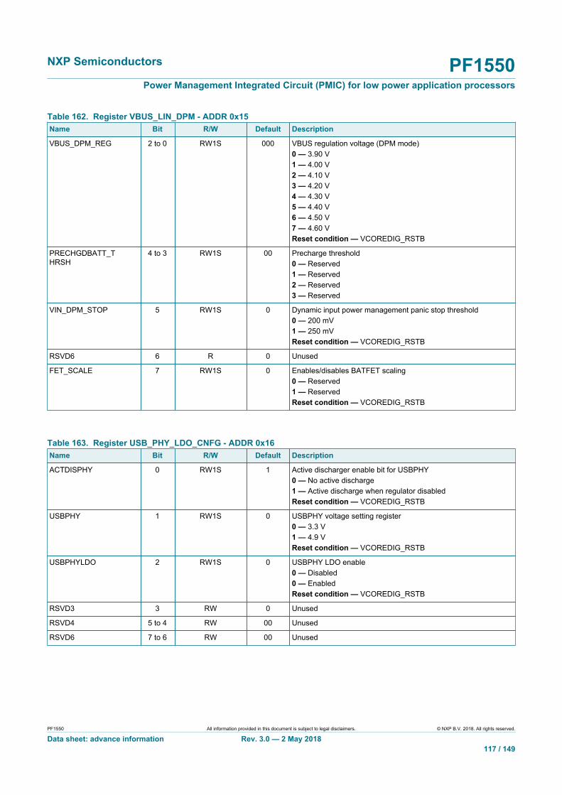
NXP Semiconductors PF1550Power Management Integrated Circuit (PMIC) for low power application processors
PF1550 All information provided in this document is subject to legal disclaimers. © NXP B.V. 2018. All rights reserved.
Data sheet: advance information Rev. 3.0 — 2 May 2018117 / 149
Table 162. Register VBUS_LIN_DPM - ADDR 0x15Name Bit R/W Default Description
VBUS_DPM_REG 2 to 0 RW1S 000 VBUS regulation voltage (DPM mode)0 — 3.90 V1 — 4.00 V2 — 4.10 V3 — 4.20 V4 — 4.30 V5 — 4.40 V6 — 4.50 V7 — 4.60 VReset condition — VCOREDIG_RSTB
PRECHGDBATT_THRSH
4 to 3 RW1S 00 Precharge threshold0 — Reserved1 — Reserved2 — Reserved3 — Reserved
VIN_DPM_STOP 5 RW1S 0 Dynamic input power management panic stop threshold0 — 200 mV1 — 250 mVReset condition — VCOREDIG_RSTB
RSVD6 6 R 0 Unused
FET_SCALE 7 RW1S 0 Enables/disables BATFET scaling0 — Reserved1 — ReservedReset condition — VCOREDIG_RSTB
Table 163. Register USB_PHY_LDO_CNFG - ADDR 0x16Name Bit R/W Default Description
ACTDISPHY 0 RW1S 1 Active discharger enable bit for USBPHY0 — No active discharge1 — Active discharge when regulator disabledReset condition — VCOREDIG_RSTB
USBPHY 1 RW1S 0 USBPHY voltage setting register0 — 3.3 V1 — 4.9 VReset condition — VCOREDIG_RSTB
USBPHYLDO 2 RW1S 0 USBPHY LDO enable0 — Disabled0 — EnabledReset condition — VCOREDIG_RSTB
RSVD3 3 RW 0 Unused
RSVD4 5 to 4 RW 00 Unused
RSVD6 7 to 6 RW 00 Unused

NXP Semiconductors PF1550Power Management Integrated Circuit (PMIC) for low power application processors
PF1550 All information provided in this document is subject to legal disclaimers. © NXP B.V. 2018. All rights reserved.
Data sheet: advance information Rev. 3.0 — 2 May 2018118 / 149
Table 164. Register DBNC_DELAY_TIME - ADDR 0x18Name Bit R/W Default Description
VBUS_OV_TDB 1 to 0 RW1S 00 VBUS overvoltage debounce delay0 — 10 µs (Reserved)1 — 100 µs2 — 1 ms3 — 10 msReset condition — VCOREDIG_RSTB
USB_PHY_TDB 3 to 2 RW1S 00 USBPHY debounce timer - not used in PF15500 — 0 ms1 — 16 ms2 — 32 ms3 — Not usedReset condition — VCOREDIG_RSTB
SYS_WKUP_DLY 5 to 4 RW1S 00 System wake-up time0 — 8.0 ms1 — 16 ms2 — 32 ms3 — 100 msReset condition — VCOREDIG_RSTB
RSVD6 7 to 6 RW 00 Unused
Table 165. Register CHG_INT_CNFG - ADDR 0x19Name Bit R/W Default Description
CHG_INT_GEN 0 RW1S 0 Determines if an interrupt is generated at every mode transition incharger0 — Interrupt is not generated at every mode transition excepttransition from Fast Charge to CV1 — Interrupt is generated at every mode transition (Fast Charge,CV, EOC, DONE, No Charger)Reset condition — VCOREDIG_RSTB
EOC_INT 1 RW1S 0 Interrupt bit generated at end-of-charge0 — No interrupt bit is generated when end-of- charge current istriggered1 — Interrupt bit is generated when end-of-charge current istriggeredReset condition — VCOREDIG_RSTB
RSVD2 7 to 2 RW 000000 Unused
Table 166. Register THM_ADJ_SETTING - ADDR 0x1AName Bit R/W Default Description
THM_WARM 0 RW1S 0 Thermistor warm threshold setting0 — 45 °C1 — 50 °CReset condition — VCOREDIG_RSTB
THM_COOL 1 RW1S 0 Thermistor cool threshold setting0 — 15 °C1 — 10 °CReset condition — VCOREDIG_RSTB

NXP Semiconductors PF1550Power Management Integrated Circuit (PMIC) for low power application processors
PF1550 All information provided in this document is subject to legal disclaimers. © NXP B.V. 2018. All rights reserved.
Data sheet: advance information Rev. 3.0 — 2 May 2018119 / 149
Name Bit R/W Default Description
CV_ADJ 3 to 2 RW1S 00 JEITA Thermistor battery termination voltage subtraction setting0 — 60 mV1 — 100 mV2 — 160 mV3 — 200 mvReset condition — VCOREDIG_RSTB
CC_ADJ 5 to 4 RW1S 00 JEITA Thermistor battery charging current setting (percentage ofI_FC)0 — 25 %1 — 50 %2 — 75 %3 — 100 %Reset condition — VCOREDIG_RSTB
RSVD6 7 to 6 RW 00 Unused
Table 167. Register VBUS2SYS_CNFG - ADDR 0x1BName Bit R/W Default Description
VBUS2SYS_TDB 1 to 0 RW1S 00 VBUS to VSYS comparator debounce time0 — Reserved1 — 100 µs2 — 1 ms3 — 10 msReset condition — VCOREDIG_RSTB
VBUS2SYS_THRSH 2 RW1S 0 VBUS to VSYS comparator threshold setting0 — 50 mV1 — 175 mVReset condition — VCOREDIG_RSTB
RSVD3 7 to 3 RW 00000 Unused

NXP Semiconductors PF1550Power Management Integrated Circuit (PMIC) for low power application processors
PF1550 All information provided in this document is subject to legal disclaimers. © NXP B.V. 2018. All rights reserved.
Data sheet: advance information Rev. 3.0 — 2 May 2018120 / 149
Table 168. Register LED_PWM - ADDR 0x1CName Bit R/W Default Description
LED_PWM 5 to 0 RW 000000 LED PWM duty cycle setting0 — 0/32 (Off)1 — 1/322 — 2/323 — 3/324 — 4/325 — 5/326 — 6/327 — 7/328 — 8/329 — 9/3210 — 10/3211 — 11/3212 — 12/3213 — 13/3214 — 14/3215 — 15/3216 — 16/3217 — 17/3218 — 18/3219 — 19/3220 — 20/3221 — 21/3222 — 22/3223 — 23/3224 — 24/3225 — 25/3226 — 26/3227 — 27/3228 — 28/3229 — 29/3230 — 30/3231 — 31/3232 and higher — 32/32Reset condition — VCOREDIG_RSTB
LED_RAMP 6 RW 0 Enable PWM ramp enable0 — Ramp disable1 — Ramp enableReset condition — VCOREDIG_RSTB
LED_EN 7 RW 0 LED driver enable0 — Disabled1 — EnabledReset condition — VCOREDIG_RSTB
Table 169. Register FAULT_BATFET_CNFG - ADDR 0x1DName Bit R/W Default Description
OVFLT_BFET_EN 0 RW1S 0 BATFET control during battery overvoltage0 — BATFET is opened during battery overvoltage1 — BATFET remains closedReset condition — VCOREDIG_RSTB

NXP Semiconductors PF1550Power Management Integrated Circuit (PMIC) for low power application processors
PF1550 All information provided in this document is subject to legal disclaimers. © NXP B.V. 2018. All rights reserved.
Data sheet: advance information Rev. 3.0 — 2 May 2018121 / 149
Name Bit R/W Default Description
WDFLT_BFET_EN 1 RW1S 0 BATFET control during watchdog fault0 — BATFET is opened during watchdog fault1 — BATFET remains closedReset condition — VCOREDIG_RSTB
THMSUS_BFET_EN 2 RW1S 0 BATFET control during thermistor fault (< Cold or > Hot)0 — BATFET is opened during battery thermistor fault1 — BATFET remains closedReset condition — VCOREDIG_RSTB
TSHDN_BFET_EN 3 RW1S 0 BATFET control during thermal shutdown0 — BATFET is opened during thermal shutdown1 — BATFET remains closedReset condition — VCOREDIG_RSTB
TMRFLT_BFET_EN 4 RW1S 0 BATFET control during charger timer fault0 — BATFET is opened during charger timer fault1 — BATFET remains closedReset condition — POR
RSVD5 5 RW1S 0 Unused
CTRL_CHGR_BETA_SEL
7 to 6 RW1S 00 Reserved
Table 170. Register LED_CNFG - ADDR 0x1EName Bit R/W Default Description
LED_FREQ 1 to 0 RW 00 LED driver PWM frequency setting0 — 1.0 Hz1 — 0.5 Hz2 — 256 Hz3 — 8.0 HzReset condition — VCOREDIG_RSTB
LED_CURRENT 3 to 2 RW1S 00 LED driver current amplitude setting0 — Reserved1 — 6.0 mA2 — Reserved3 — ReservedReset condition — VCOREDIG_RSTB
LED_CFG 4 RW1S 0 Controls LED on/blinking mode0 — LED on during charging; flashing during charger fault; off inDONE state1 — LED flashing during charging; on during charger fault; off inDONE stateReset condition — VCOREDIG_RSTB
LEDOVRD 5 RW 0 Enable software control of LED0 — LED controlled by state machine1 — LED controlled via softwareReset condition — VCOREDIG_RSTB
RSVD4 7 to 6 RW 00 Unused

NXP Semiconductors PF1550Power Management Integrated Circuit (PMIC) for low power application processors
PF1550 All information provided in this document is subject to legal disclaimers. © NXP B.V. 2018. All rights reserved.
Data sheet: advance information Rev. 3.0 — 2 May 2018122 / 149
Table 171. Register LED_CNFG - ADDR 0x1FName Bit R/W Default Description
CHGR_KEY2 7 to 0 RW 0x00 Reserved
12.3 Register PMIC bitmap
VCOREDIG_PORB [1]
PS_END_RSTB [2]
REGS_DISABLE_TOG_RSTB [3]
[1] Bits reset by invalid VCOREDIG[2] Bits reset by PORB or RESETBMCU[3] Bits reset by pulse to REGS_DISABLE mode
Table 172. Register PMIC bitmapBITS[7:0]Addr
essRegister name
7 6 5 4 3 2 1 0
Name FAMILY[3:7] DEVICE_ID[2:0]
Reset 0 1 1 1 1 1 0 0
0x00 DEVICE_ID
Type R R R R R R R R
Name — — OTP_FLAVOR[5:0]
Reset 0 0 0 0 0 0 0 0
0x01 OTP_FLAVOR
Type — — R R R R R R
Name FAB_FIN[7:6] FULL_LAYER_REV[5:3] METAL_LAYER_REV[2:0]
Reset 0 0 0 0 1 0 0 0
0x02 SILICON_REV
Type R R R R R R R R
Name MISC_INT TEMP_INT ONKEY_INT LDO_INT SW3_INT SW2_INT SW1_INT CHG_INT
Reset 0 0 0 0 0 0 0 0
0x06 INT_CATEGORY
Type R R R R R R R R
Name — — — — — SW3_LS_I SW2_LS_I SW1_LS_I
Reset 0 0 0 0 0 0 0 0
0x08 SW_INT_STAT0
Type — — — — — RW1C RW1C RW1C
Name — — — — — SW3_LS_M SW2_LS_M SW1_LS_M
Reset 0 0 0 0 0 1 1 1
0x09 SW_INT_MASK0
Type — — — — — RW RW RW
Name — — — — — SW3_LS_S SW2_LS_S SW1_LS_S
Reset 0 0 0 0 0 0 0 0
0x0A SW_INT_SENSE0
Type — — — — — R R R
Name — — — — — SW3_HS_I SW2_HS_I SW1_HS_I
Reset 0 0 0 0 0 0 0 0
0x0B SW_INT_STAT1
Type — — — — — RW1C RW1C RW1C
Name — — — — — SW3_HS_M SW2_HS_M SW1_HS_M
Reset 0 0 0 0 0 1 1 1
0x0C SW_INT_MASK1
Type — — — — — RW RW RW
Name — — — — — SW3_HS_S SW2_HS_S SW1_HS_S
Reset 0 0 0 0 0 0 0 0
0x0D SW_INT_SENSE1
Type — — — — — R R R
Name — — — — — — SW2_DVS_DONE_I
SW1_DVS_DONE_I
Reset 0 0 0 0 0 0 0 0
0x0E SW_INT_STAT2
Type — — — — — — RW1C RW1C
Name — — — — — — SW2_DVS_DONE_M
SW1_DVS_DONE_M
Reset 0 0 0 0 0 0 1 1
0x0F SW_INT_MASK2
Type — — — — — — RW RW

NXP Semiconductors PF1550Power Management Integrated Circuit (PMIC) for low power application processors
PF1550 All information provided in this document is subject to legal disclaimers. © NXP B.V. 2018. All rights reserved.
Data sheet: advance information Rev. 3.0 — 2 May 2018123 / 149
BITS[7:0]Address
Register name
7 6 5 4 3 2 1 0
Name — — — — — — SW2_DVS_S SW1_DVS_S
Reset 0 0 0 0 0 0 0 0
0x10 SW_INT_SENSE2
Type — — — — — — R R
Name — — — — — LDO3_FAULTI LDO2_FAULTI LDO1_FAULTI
Reset 0 0 0 0 0 0 0 0
0x18 LDO_INT_STAT0
Type — — — — — RW1C RW1C RW1C
Name — — — — — LDO3_FAULTM LDO2_FAULTM LDO1_FAULTM
Reset 0 0 0 0 0 1 1 1
0x19 LDO_INT_MASK0
Type — — — — — RW RW RW
Name — — — — — LDO3_FAULTS LDO2_FAULTS LDO1_FAULTS
Reset 0 0 0 0 0 0 0 0
0x1A LDO_INT_SENSE0
Type — — — — — R R R
Name — — — — — THERM125I — THERM110I
Reset 0 0 0 0 0 0 0 0
0x20 TEMP_INT_STAT0
Type — — — — — RW1C — RW1C
Name — — — — — THERM125M — THERM110M
Reset 0 0 0 0 1 1 1 1
0x21 TEMP_INT_MASK0
Type — — — — — RW — RW
0x22 TEMP_INT_SENSE0
Name — — — — — THERM125S — THERM110S
Reset 0 0 0 0 0 0 0 0
Type — — — — — R — R
Name — — ONKEY_8SI ONKEY_4SI ONKEY_3SI ONKEY_2SI ONKEY_1SI ONKEY_PUSHI
Reset 0 0 0 0 0 0 0 0
0x24 ONKEY_INT_STAT0
Type — — RW1C RW1C RW1C RW1C RW1C RW1C
Name — — ONKEY_8SM ONKEY_4SM ONKEY_3SM ONKEY_2SM ONKEY_1SM ONKEY_PUSHM
Reset 0 0 1 1 1 1 1 1
0x25 ONKEY_INT_MASK0
Type — — RW RW RW RW RW RW
Name — — ONKEY_8SS ONKEY_4SS ONKEY_3SS ONKEY_2SS ONKEY_1SS ONKEY_PUSHS
Reset 0 0 0 0 0 0 0 0
0x26 ONKEY_INT_SENSE0
Type — — R R R R R R
Name — — — SYS_OVLO_I LOW_SYS_WARN_I
PWRON_I PWRDN_I PWRUP_I
Reset 0 0 0 0 0 0 0 0
0x28 MISC_INT_STAT0
Type — — — RW1C RW1C RW1C RW1C RW1C
Name — — — SYS_OVLO_M LOW_SYS_WARN_M
PWRON_M PWRDN_M PWRUP_M
Reset 0 0 0 1 1 1 1 1
0x29 MISC_INT_MASK0
Type — — — RW RW RW RW RW
Name — — — SYS_OVLO_S LOW_SYS_WARN_S
PWRON_S PWRDN_S PWRUP_S
Reset 0 0 0 0 0 0 0 0
0x2A MISC_INT_SENSE0
Type — — — R R R R R
Name COINCHEN VCOIN[3:0]
Reset 0 0 0 0 0 0 0 0
0x30 COINCELL_CONTROL
Type — — — RW RW RW RW RW
Name — — SW1_VOLT[5:0]
Reset 0 0 0 0 0 0 0 0
0x32 SW1_VOLT
Type — — RW1S RW1S RW1S RW1S RW1S RW1S
Name — — SW1_STBY_VOLT[5:0]
Reset 0 0 0 0 0 0 0 0
0x33 SW1_STBY_VOLT
Type — — RW1S RW1S RW1S RW1S RW1S RW1S
Name — — SW1_SLP_VOLT[5:0]
Reset 0 0 0 0 0 0 0 0
0x34 SW1_SLP_VOLT
Type — — RW1S RW1S RW1S RW1S RW1S RW1S
Name SW1_RDIS_ENB SW1_FPWM SW1_FPWM_IN_DVS
SW1_DVSSPEED
SW1_LPWR SW1_OMODE SW1_STBY_EN SW1_EN
Reset 0 0 0 0 0 0 0 0
0x35 SW1_CTRL
Type RW1S RW RW RW1S RW RW RW1S RW1S

NXP Semiconductors PF1550Power Management Integrated Circuit (PMIC) for low power application processors
PF1550 All information provided in this document is subject to legal disclaimers. © NXP B.V. 2018. All rights reserved.
Data sheet: advance information Rev. 3.0 — 2 May 2018124 / 149
BITS[7:0]Address
Register name
7 6 5 4 3 2 1 0
Name — — — SW1_TMODE_SEL — — SW1_ILIM[1:0]
Reset 0 0 0 0 0 0 0 0
0x36 SW1_CTRL1
Type — — — RW — — RW1S RW1S
Name — — SW2_VOLT[5:0]
Reset 0 0 0 0 0 0 0 0
0x38 SW2_VOLT
Type — — RW1S RW1S RW1S RW1S RW1S RW1S
Name — — SW2_STBY_VOLT[5:0]
Reset 0 0 0 0 0 0 0 0
0x39 SW2_STBY_VOLT
Type — — RW1S RW1S RW1S RW1S RW1S RW1S
Name — — SW2_SLP_VOLT[5:0]
Reset 0 0 0 0 0 0 0 0
0x3A SW2_SLP_VOLT
Type — — RW1S RW1S RW1S RW1S RW1S RW1S
Name SW2_RDIS_ENB SW2_FPWM SW2_FPWM_IN_DVS
SW2_DVSSPEED
SW2_LPWR SW2_OMODE SW2_STBY_EN SW2_EN
Reset 0 0 0 0 0 0 0 0
0x3B SW2_CTRL
Type RW1S RW RW RW1S RW RW RW1S RW1S
Name — — — SW2_TMODE_SEL — — SW2_ILIM[1:0]
Reset 0 0 0 0 0 0 0 0
0x3C SW2_CTRL1
Type — — — RW — — RW1S RW1S
Name — — — — SW3_VOLT[3:0]
Reset 0 0 0 0 0 0 0 0
0x3E SW3_VOLT
Type — — — — RW1S RW1S RW1S RW1S
Name — — — — SW3_STBY_VOLT[3:0]
Reset 0 0 0 0 0 0 0 0
0x3F SW3_STBY_VOLT
Type — — — — RW1S RW1S RW1S RW1S
Name — — — — SW3_SLP_VOLT[3:0]
Reset 0 0 0 0 0 0 0 0
0x40 SW3_SLP_VOLT
Type — — — — RW1S RW1S RW1S RW1S
Name SW3_RDIS_ENB SW3_FPWM — SW3_DVSSPEED
SW3_LPWR SW3_OMODE SW3_STBY_EN SW3_EN
Reset 0 0 0 0 0 0 0 0
0x41 SW3_CTRL
Type RW1S RW — RW1S RW RW RW1S RW1S
Name — — — SW3_TMODE_SEL — — SW3_ILIM[1:0]
Reset 0 0 0 0 0 0 0 0
0x42 SW3_CTRL1
Type — — — RW — — RW1S RW1S
Name — — LIBGDIS FORCEBOS CLKPULSE VSNVS_VOLT[2:0]
Reset 0 0 0 0 0 0 0 0
0x48 VSNVS_CTRL
Type — — RW RW RW RW1S RW1S RW1S
Name — — — — VREFDDR_LPWR
VREFDDR_OMODE
VREFDDR_STBY_EN
VREFDDR_EN
Reset 0 0 0 0 0 0 0 0
0x4A VREFDDR_CTRL
Type — — — — RW RW RW1S RW1S
Name — — — LDO1_VOLT[4:0]
Reset 0 0 0 0 0 0 0 0
0x4C LDO1_VOLT
Type — — — RW1S RW1S RW1S RW1S RW1S
Name — — — LDO1_LS_EN LDO1_LPWR LDO1_OMODE LDO1_STB Y_EN VLDO1_EN
Reset 0 0 0 0 0 0 0 0
0x4D LDO1_CTRL
Type — — — RW1S RW RW RW1S RW1S
Name — — — — LDO2_VOLT[3:0]
Reset 0 0 0 0 0 0 0 0
0x4F LDO2_VOLT
Type — — — — RW1S RW1S RW1S RW1S
Name — — — — LDO2_LPWR LDO2_OMODE LDO2_STB Y_EN VLDO2_EN
Reset 0 0 0 0 0 0 0 0
0x50 LDO2_CTRL
Type — — — — RW RW RW1S RW1S
Name — — — LDO3_VOLT[4:0]
Reset 0 0 0 0 0 0 0 0
0x52 LDO3_VOLT
Type — — — RW1S RW1S RW1S RW1S RW1S
Name — — — LDO3_LS_EN LDO3_LPWR LDO3_OMODE LDO3_STB Y_EN VLDO3_EN
Reset 0 0 0 0 0 0 0 0
0x53 LDO3_CTRL
Type — — — RW1S RW RW RW1S RW1S

NXP Semiconductors PF1550Power Management Integrated Circuit (PMIC) for low power application processors
PF1550 All information provided in this document is subject to legal disclaimers. © NXP B.V. 2018. All rights reserved.
Data sheet: advance information Rev. 3.0 — 2 May 2018125 / 149
BITS[7:0]Address
Register name
7 6 5 4 3 2 1 0
Name TGRESET[7:6] POR_DLY[5:3] STANDBYINV STANDBYDLY[1:0]
Reset 0 0 0 0 0 0 0 1
0x58 PWRCTRL0
Type RW1S RW1S RW1S RW1S RW1S RW RW RW
Name ONKEY_RST_EN REGSCPEN RESTARTEN PWRONRSTEN ONKEYDBNC[3:2] PWRONDBNC[1:0]
Reset 1 0 0 0 0 0 0 0
0x59 PWRCTRL1
Type RW RW RW RW RW RW RW RW
Name — — — — LOW_SYS_WARN[3:2] UVDET[1:0]
Reset 0 0 0 0 0 0 0 0
015A PWRCTRL2
Type — — — — RW RW RW1S RW1S
Name — GOTO_CORE_OFF
GOTO_SHIP
Reset 0 0 0 0 0 0 0 0
0x5B PWRCTRL3
Type RW RW RW RW RW RW RW RW
Name — — — — — SW1_PWRDN_SEQ[2:0]
Reset 0 0 0 0 0 0 0 0
0x5F SW1_PWRDN_SEQ
Type — — — — — RW1S RW1S RW1S
Name — — — — — SW2_PWRDN_SEQ[2:0]
Reset 0 0 0 0 0 0 0 0
0x60 SW2_PWRDN_SEQ
Type — — — — — RW1S RW1S RW1S
Name — — — — — SW3_PWRDN_SEQ[2:0]
Reset 0 0 0 0 0 0 0 0
0x61 SW3_PWRDN_SEQ
Type — — — — — RW1S RW1S RW1S
Name — — — — — LDO1_PWRDN_SEQ[2:0]
Reset 0 0 0 0 0 0 0 0
0x62 LDO1_PWRDN_SEQ
Type — — — — — RW1S RW1S RW1S
Name — — — — — LDO2_PWRDN_SEQ[2:0]
Reset 0 0 0 0 0 0 0 0
0x63 LDO2_PWRDN_SEQ
Type — — — — — RW1S RW1S RW1S
Name — — — — — LDO3_PWRDN_SEQ[2:0]
Reset 0 0 0 0 0 0 0 0
0x64 LDO3_PWRDN_SEQ
Type — — — — — RW1S RW1S RW1S
Name — — — — — VREFDDR_PWRDN_SEQ[2:0]
Reset 0 0 0 0 0 0 0 0
0x65 VREFDDR_PWRDN_S EQ
Type — — — — — RW1S RW1S RW1S
Name — — STATE[5:0]
Reset 0 0 0 0 0 0 0 0
0x67 STATE_INFO
Type — — R R R R R R
Name USE_DEFAULT_ADDR
— — — — I2C_SLAVE_ADDR_LSBS[2:0]
Reset 0 0 0 0 0 0 0 0
0x68 I2C_ADDR
Type RW — — — — R R R
Name — — — — — — — —
Reset 0 0 0 0 0 0 0 0
0x69 IO_DRV0
Type RW RW RW RW RW RW RW RW
Name — — — — — — — —
Reset 0 0 0 0 0 0 0 0
0x6A IO_DRV1
Type — — — — — — RW RW
Name — — — — — REQ_ACORE_HIPWR
REQ_ACORE_ON REQ_16MHZ
Reset 0 0 0 0 0 0 0 0
0x6B RC_16MHZ
Type — — — — — RW RW RW
Name KEY1[7:0]
Reset 0 0 0 0 0 0 0 0
0x6F KEY1
Type RW RW RW RW RW RW RW RW

NXP Semiconductors PF1550Power Management Integrated Circuit (PMIC) for low power application processors
PF1550 All information provided in this document is subject to legal disclaimers. © NXP B.V. 2018. All rights reserved.
Data sheet: advance information Rev. 3.0 — 2 May 2018126 / 149
12.4 Register charger bitmap
CHGPOK_RSTB [1]
VCOREDIG_RSTB [2]
[1] Bits reset by invalid VBUSIN[2] Bits reset by invalid VCOREDIG
Table 173. Register charger bitmapBITS[7:0]Address Register name
7 6 5 4 3 2 1 0
Name THM_I VBUS_DPM_I VBUS_I RSVD4 CHG_I BAT_I BAT2SOC_I SUP_I
Reset 0 0 0 0 0 0 0 0
0x00 CHG_INT
Type RW1C RW1C RW1C RW1C RW1C RW1C RW1C RW1C
Name THM_M VBUS_DPM_M VBUS_M RSVD4 CHG_M BAT_M BAT2SOC_M SUP_M
Reset 1 1 1 1 1 1 1 1
0x02 CHG_INT_MASK
Type RW RW RW RW RW RW RW RW
Name THM_OK VBUS_DPM_OK VBUS_OK RSVD4 CHG_OK BAT_OK BAT2SOC_OK SUP_OK
Reset 1 0 0 0 0 1 0 0
0x04 CHG_INT_OK
Type R R R R R R R R
Name VBUS_DPM_SNS
RSVD6 VBUS_VALID_SNS
VBUS_OVLO_SNS
VBUS_IN2SYS_SNS
VBUS_UVLO_SNS
RSVD0[1:0]
Reset 0 0 0 0 1 1 0 0
0x06 VBUS_SNS
Type R R R R R R R R
Name TREG_SNS THM_SNS WDT_SNS RSVD4 CHG_SNS[3:0]
Reset 0 0 0 0 1 0 0 0
0x07 CHG_SNS
Type R R R R R R R R
Name RSVD6[7:6] BATTOC_SNS RSVD3[4:3] BATT_SNS[2:0]
Reset 0 0 0 0 0 0 0 0
0x08 BATT_SNS
Type RW RW R RW RW R R R
Name RSVD5[7:5] DISBATFET WDTEN RSVD2 CHG_OPER[1:0]
Reset 0 0 0 0 0 0 0 1
0x09 CHG_OPER
Type RW RW RW RW RW RW RW1S RW1S
Name TPRECHG RSVD6 EOCTIME[5:3]FCHGTIME[2:0]
Reset 0 0 0 0 1 0 1 0
0x0A CHG_TMR
Type RW1S R RW1S RW1S RW1S RW1S RW1S RW1S
Name EOC_MODE IEOC[6:4] EOC_EXIT FORCE_BATT_ISO
CHG_RESTART[1:0]
Reset 0 1 0 0 0 0 0 1
0x0D CHG_EOC_CNFG
Type RW1S RW RW RW RW1S RW1S RW1S RW1S
Name RSVD7 PRECHGLB_THRSH[6:5] CHG_CC[4:0]
Reset 0 0 0 0 0 0 0 0
0x0E CHG_CURR_CNFG
Type RW RW1S RW1S RW1S RW1S RW1S RW1S RW1S
Name MINVSYS[7:6] CHGCV[5:0]
Reset 0 0 1 0 1 0 1 1
0x0F BATT_REG
Type RW1S RW1S RW1S RW1S RW1S RW1S RW1S RW1S
Name BOVRC_NOVBUS
WD_TIME BATFET_OC[5:4] BOVRC_DISBATFET
WD_BATFET_OFF
WDTCLR[1:0]
Reset 0 0 1 1 0 0 0 0
0x11 BATFET_CNFG
Type RW RW RW1S RW1S RW1S RW RW RW
Name TEMP_FB_EN RSVD6 THM_HOT THM_COLD REGTEMP[3:2] THM_CNFG[1:0]
Reset 0 0 0 0 0 1 0 1
0x12 THM_REG_CNFG
Type RW1S RW RW1S RW1S RW1S RW1S RW1S RW1S
Name VBUS_LIN_ILIM[7:3] RSVD0[2:0]
Reset 0 1 1 0 1 0 0 0
0x14 VBUS_INLIM_CNFG
Type RW1S RW1S RW1S RW1S RW1S RW RW RW

NXP Semiconductors PF1550Power Management Integrated Circuit (PMIC) for low power application processors
PF1550 All information provided in this document is subject to legal disclaimers. © NXP B.V. 2018. All rights reserved.
Data sheet: advance information Rev. 3.0 — 2 May 2018127 / 149
BITS[7:0]Address Register name
7 6 5 4 3 2 1 0
Name FET_SCALE RSVD6 VIN_DPM_STOP
PRECHGDBATT_THRSH[4:3] VBUS_DPM_REG[2:0]
Reset 0 0 0 0 0 0 0 0
0x15 VBUS_LIN_DPM
Type RW1S R RW1S RW1S RW1S RW1S RW1S RW1S
Name RSVD6[7:6] RSVD4[5:4] RSVD3 USBPHYLDO USBPHY ACTDISPHY
Reset 0 0 0 0 0 0 0 1
0x16 USB_PHY_LDO_CNFG
Type RW RW RW RW RW RW1S RW1S RW1S
Name RSVD6[7:6] SYS_WKUP_DLY[5:4] USB_PHY_TDB[3:2] VBUS_OV_TDB[1:0]
Reset 0 0 0 0 0 0 0 0
0x18 DBNC_DELAY_TIME
Type RW RW RW1S RW1S RW1S RW1S RW1S RW1S
Name RSVD2[7:2] EOC_INT CHG_INT_GEN
Reset 0 0 0 0 0 0 0 0
0x19 CHG_INT_CNFG
Type RW RW RW RW RW RW RW1S RW1S
0x1A THM_ADJ_SETTING Name RSVD6[7:6] CC_ADJ[5:4] CV_ADJ[3:2] THM_COOL THM_WARM
Reset 0 0 0 0 0 0 0 0
Type RW RW RW1S RW1S RW1S RW1S RW1S RW1S
Name RSVD3[7:3] VBUS2SYS_THRSH
VBUS2SYS_TDB[1:0]
Reset 0 0 0 0 0 0 0 0
0x1B VBUS2SYS_CNFG
Type RW RW RW RW RW RW1S RW1S RW1S
Name LED_EN LED_RAMP LED_PWM[5:0]
Reset 0 0 0 0 0 0 0 0
0x1C LED_PWM
Type RW RW RW RW RW RW RW RW
Name CTRL_CHGR_BETA_SEL[7:6] RSVD5 TMRFLT_BFET_EN
TSHDN_BFET_EN
THMSUS_BFET_EN
WDFLT_BFEET_EN
OVFLT_BFEET_EN
Reset 0 0 0 0 0 0 0 0
0x1D FAULT_BATFET_CNFG
Type RW1S RW1S RW1S RW1S RW1S RW1S RW1S RW1S
Name RSVD4[7:6] LEDOVRD LED_CFG LED_CURRENT[3:2] LED_FREQ[1:0]
Reset 0 0 0 0 0 0 0 0
0x1E LED_CNFG
Type RW RW RW RW1S RW1S RW1S RW RW
Name CHGR_KEY2[7:0]
Reset 0 0 0 0 0 0 0 0
0x1F CHGR_KEY2
Type RW RW RW RW RW RW RW RW

NXP Semiconductors PF1550Power Management Integrated Circuit (PMIC) for low power application processors
PF1550 All information provided in this document is subject to legal disclaimers. © NXP B.V. 2018. All rights reserved.
Data sheet: advance information Rev. 3.0 — 2 May 2018128 / 149
12.5 Register OTP bitmap
Table 174. Register OTP bitmapBIT[7:0]Address Register name Value
7 6 5 4 3 2 1 0
0x1C OTP_PMIC_CFG0
UNUSED UNUSED UNUSED OTP_PWRGD_EN
OTP_SEQ_CLK_SPEED
OTP_PWRON_CFG
A1 (Default) 0x00 0 0 0 0 0 0 0 0
A2 0x04 0 0 0 0 0 1 0 0
A3 0x04 0 0 0 0 0 1 0 0
A4 0x04 0 0 0 0 0 1 0 0
A5 0x04 0 0 0 0 0 1 0 0
A6 0x04 0 0 0 0 0 1 0 0
A7 0x04 0 0 0 0 0 1 0 0
0x1D OTP_SW1 OTP_SW1_DVSSPEED
OTP_SW1_RDIS_ENB
OTP_SW1_VOLT[5:0]
A1 (Default) 0x80 1 0 0 0 0 0 0 0
A2 0xA0 1 0 1 0 0 0 0 0
A3 0XBF 1 0 1 1 1 1 1 1
A4 0XA8 1 0 1 0 1 0 0 0
A5 0XBF 1 0 1 1 1 1 1 1
A6 0XB6 1 0 1 1 0 1 1 0
A7 0XBF 1 0 1 1 1 1 1 1
0x1E OTP_SW1_SW2 OTP_SW2_VOLT[5:0] OTP_SW1_DVS_SEL
OTP_SW1_EN_AND_STBY_EN
A1 (Default) 0XA3 1 0 1 0 0 0 1 1
A2 0x05 0 0 0 0 0 1 0 1
A3 0x09 0 0 0 0 1 0 0 1
A4 0xC1 1 1 0 0 0 0 0 1
A5 0x0D 0 0 0 0 1 1 0 1
A6 0x09 0 0 0 0 1 0 0 1
A7 0x05 0 0 0 0 0 1 0 1
0x1F OTP_SW2_SW3 OTP_SW3_VOLT[3:0] OTP_SW2_DVS_SEL
OTP_SW2_EN_AND_STBY_EN
OTP_SW2_DVSSPEED
OTP_SW2_RDIS_ENB
A1 (Default) 0x04 0 0 0 0 0 1 0 0
A2 0x0E 0 0 0 0 1 1 1 0
A3 0xFE 1 1 1 1 1 1 1 0
A4 0x06 0 0 0 0 0 1 1 0
A5 0xFE 1 1 1 1 1 1 1 0
A6 0xFE 1 1 1 1 1 1 1 0
A7 0x0E 0 0 0 0 1 1 1 0
0x20 OTP_SW3__SWxILIM
OTP_SW3_ILIM[1:0] OTP_SW2_ILIM[1:0] OTP_SW1_ILIM[1:0] OTP_SW3_EN_AND_STBY_EN
OTP_SW3_RDIS_ENB
A1 (Default) 0XFE 1 1 1 1 1 1 1 0
A2 0xFE 1 1 1 1 1 1 1 0
A3 0xFE 1 1 1 1 1 1 1 0
A4 0xFE 1 1 1 1 1 1 1 0
A5 0xFE 1 1 1 1 1 1 1 0
A6 0xFE 1 1 1 1 1 1 1 0
A7 0xFE 1 1 1 1 1 1 1 0
0x21 OTP_VREF_LDO1
OTP_LDO1_LS_EN OTP_LDO1_VOLT[4:0] OTP_VREFDDREN_AND_STBY_EN
UNUSED
A1 (Default) 0x16 0 0 0 1 0 1 1 0
A2 0x42 0 1 0 0 0 0 1 0
A3 0x42 0 1 0 0 0 0 1 0
A4 0x7E 0 1 1 1 1 1 1 0
A5 0x42 0 1 0 0 0 0 1 0
A6 0x42 0 1 0 0 0 0 1 0
A7 0x7E 0 1 1 1 1 1 1 0
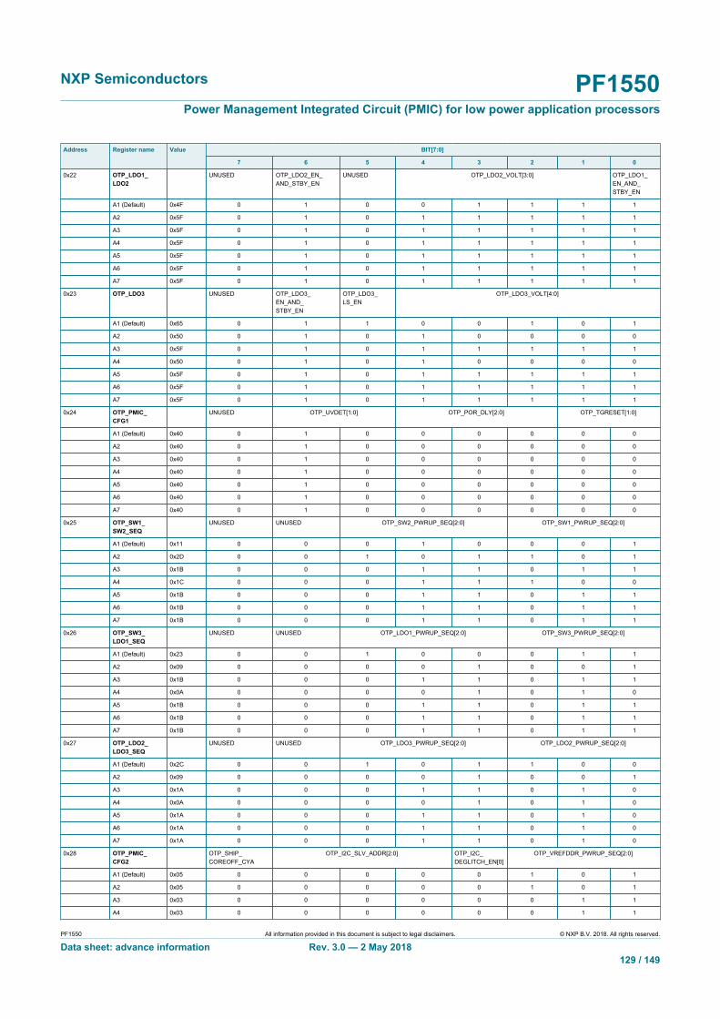
NXP Semiconductors PF1550Power Management Integrated Circuit (PMIC) for low power application processors
PF1550 All information provided in this document is subject to legal disclaimers. © NXP B.V. 2018. All rights reserved.
Data sheet: advance information Rev. 3.0 — 2 May 2018129 / 149
BIT[7:0]Address Register name Value
7 6 5 4 3 2 1 0
0x22 OTP_LDO1_LDO2
UNUSED OTP_LDO2_EN_AND_STBY_EN
UNUSED OTP_LDO2_VOLT[3:0] OTP_LDO1_EN_AND_STBY_EN
A1 (Default) 0x4F 0 1 0 0 1 1 1 1
A2 0x5F 0 1 0 1 1 1 1 1
A3 0x5F 0 1 0 1 1 1 1 1
A4 0x5F 0 1 0 1 1 1 1 1
A5 0x5F 0 1 0 1 1 1 1 1
A6 0x5F 0 1 0 1 1 1 1 1
A7 0x5F 0 1 0 1 1 1 1 1
0x23 OTP_LDO3 UNUSED OTP_LDO3_EN_AND_STBY_EN
OTP_LDO3_LS_EN
OTP_LDO3_VOLT[4:0]
A1 (Default) 0x65 0 1 1 0 0 1 0 1
A2 0x50 0 1 0 1 0 0 0 0
A3 0x5F 0 1 0 1 1 1 1 1
A4 0x50 0 1 0 1 0 0 0 0
A5 0x5F 0 1 0 1 1 1 1 1
A6 0x5F 0 1 0 1 1 1 1 1
A7 0x5F 0 1 0 1 1 1 1 1
0x24 OTP_PMIC_CFG1
UNUSED OTP_UVDET[1:0] OTP_POR_DLY[2:0] OTP_TGRESET[1:0]
A1 (Default) 0x40 0 1 0 0 0 0 0 0
A2 0x40 0 1 0 0 0 0 0 0
A3 0x40 0 1 0 0 0 0 0 0
A4 0x40 0 1 0 0 0 0 0 0
A5 0x40 0 1 0 0 0 0 0 0
A6 0x40 0 1 0 0 0 0 0 0
A7 0x40 0 1 0 0 0 0 0 0
0x25 OTP_SW1_SW2_SEQ
UNUSED UNUSED OTP_SW2_PWRUP_SEQ[2:0] OTP_SW1_PWRUP_SEQ[2:0]
A1 (Default) 0x11 0 0 0 1 0 0 0 1
A2 0x2D 0 0 1 0 1 1 0 1
A3 0x1B 0 0 0 1 1 0 1 1
A4 0x1C 0 0 0 1 1 1 0 0
A5 0x1B 0 0 0 1 1 0 1 1
A6 0x1B 0 0 0 1 1 0 1 1
A7 0x1B 0 0 0 1 1 0 1 1
0x26 OTP_SW3_LDO1_SEQ
UNUSED UNUSED OTP_LDO1_PWRUP_SEQ[2:0] OTP_SW3_PWRUP_SEQ[2:0]
A1 (Default) 0x23 0 0 1 0 0 0 1 1
A2 0x09 0 0 0 0 1 0 0 1
A3 0x1B 0 0 0 1 1 0 1 1
A4 0x0A 0 0 0 0 1 0 1 0
A5 0x1B 0 0 0 1 1 0 1 1
A6 0x1B 0 0 0 1 1 0 1 1
A7 0x1B 0 0 0 1 1 0 1 1
0x27 OTP_LDO2_LDO3_SEQ
UNUSED UNUSED OTP_LDO3_PWRUP_SEQ[2:0] OTP_LDO2_PWRUP_SEQ[2:0]
A1 (Default) 0x2C 0 0 1 0 1 1 0 0
A2 0x09 0 0 0 0 1 0 0 1
A3 0x1A 0 0 0 1 1 0 1 0
A4 0x0A 0 0 0 0 1 0 1 0
A5 0x1A 0 0 0 1 1 0 1 0
A6 0x1A 0 0 0 1 1 0 1 0
A7 0x1A 0 0 0 1 1 0 1 0
0x28 OTP_PMIC_CFG2
OTP_SHIP_COREOFF_CYA
OTP_I2C_SLV_ADDR[2:0] OTP_I2C_DEGLITCH_EN[0]
OTP_VREFDDR_PWRUP_SEQ[2:0]
A1 (Default) 0x05 0 0 0 0 0 1 0 1
A2 0x05 0 0 0 0 0 1 0 1
A3 0x03 0 0 0 0 0 0 1 1
A4 0x03 0 0 0 0 0 0 1 1

NXP Semiconductors PF1550Power Management Integrated Circuit (PMIC) for low power application processors
PF1550 All information provided in this document is subject to legal disclaimers. © NXP B.V. 2018. All rights reserved.
Data sheet: advance information Rev. 3.0 — 2 May 2018130 / 149
BIT[7:0]Address Register name Value
7 6 5 4 3 2 1 0
A5 0x03 0 0 0 0 0 0 1 1
A6 0x03 0 0 0 0 0 0 1 1
A7 0x03 0 0 0 0 0 0 1 1
0x29 RSVD UNUSED UNUSED UNUSED UNUSED Reserved (OTP_VSNVS_VOLT[2:0]) Reserved(OTP_FORCE_LICELL)
A1 (Default) 0x00 0 0 0 0 0 0 0 0
A2 0x00 0 0 0 0 0 0 0 0
A3 0x00 0 0 0 0 0 0 0 0
A4 0x00 0 0 0 0 0 0 0 0
A5 0x00 0 0 0 0 0 0 0 0
A6 0x00 0 0 0 0 0 0 0 0
A7 0x00 0 0 0 0 0 0 0 0
0x2A RSVD OTP_PMIC_SPARE0[7:0]
A1 (Default) 0x00 0 0 0 0 0 0 0 0
A2 0x00 0 0 0 0 0 0 0 0
A3 0x00 0 0 0 0 0 0 0 0
A4 0x00 0 0 0 0 0 0 0 0
A5 0x00 0 0 0 0 0 0 0 0
A6 0x00 0 0 0 0 0 0 0 0
A7 0x00 0 0 0 0 0 0 0 0
0x2B OTP_CHG_CFG0 Reserved(OTP_CHGR_THM_WARM)
Reserved(OTP_CHGR_THM_COOL)
OTP_CHGR_EOCTIME[2:0] OTP_CHGR_TPRECHG
OTP_CHGR_OPER[1:0]
A1 (Default) 0x02 0 0 0 0 0 0 1 0
A2 0x01 0 0 0 0 0 0 0 1
A3 0x02 0 0 0 0 0 0 1 0
A4 0x02 0 0 0 0 0 0 1 0
A5 0x02 0 0 0 0 0 0 1 0
A6 0x01 0 0 0 0 0 0 0 1
A7 0x02 0 0 0 0 0 0 1 0
0x2C OTP_CHG_CFG1 OTP_CHGR_CHG_RESTART[1:0] Reserved(OTP_CHGR_FORCE_BATT_ISO)
Reserved(OTP_CHGR_EOC_EXIT)
Reserved(OTP_CHGR_EOC_MODE)
OTP_CHGR_FCHGTIME[2:0]
A1 (Default) 0x00 0 0 0 0 0 0 0 0
A2 0x00 0 0 0 0 0 0 0 0
A3 0x00 0 0 0 0 0 0 0 0
A4 0x00 0 0 0 0 0 0 0 0
A5 0x00 0 0 0 0 0 0 0 0
A6 0x00 0 0 0 0 0 0 0 0
A7 0x00 0 0 0 0 0 0 0 0
0x2D OTP_CHG_CFG2 OTP_CHGR_VSYSMIN[1:0] OTP_CHGR_CHG_CC[4:0] OTP_CHGR_TEMPFB_EN
A1 (Default) 0x80 1 0 0 0 0 0 0 0
A2 0x80 1 0 0 0 0 0 0 0
A3 0x80 1 0 0 0 0 0 0 0
A4 0x90 1 0 0 1 0 0 0 0
A5 0x80 1 0 0 0 0 0 0 0
A6 0x40 0 1 0 0 0 0 0 0
A7 0x80 1 0 0 0 0 0 0 0
0x2E OTP_CHG_CFG3 OTP_CHGR_BATFET_OC[1:0] OTP_CHGR_CHGCV[5:0]
A1 (Default) 0x2B 0 0 1 0 1 0 1 1
A2 0x2B 0 0 1 0 1 0 1 1
A3 0x2B 0 0 1 0 1 0 1 1
A4 0x2B 0 0 1 0 1 0 1 1
A5 0x2B 0 0 1 0 1 0 1 1
A6 0x2B 0 0 1 0 1 0 1 1
A7 0x2B 0 0 1 0 1 0 1 1
0x2F OTP_CHG_CFG4 UNUSED OTP_CHGR_THM_CNFG[1:0] OTP_CHGR_REGTEMP[1:0] OTP_CHGR_THM_COLD
OTP_CHGR_THM_HOT
OTP_CHGR_BOVRC_DISBATFET
A1 (Default) 0x00 0 0 0 0 0 0 0 0

NXP Semiconductors PF1550Power Management Integrated Circuit (PMIC) for low power application processors
PF1550 All information provided in this document is subject to legal disclaimers. © NXP B.V. 2018. All rights reserved.
Data sheet: advance information Rev. 3.0 — 2 May 2018131 / 149
BIT[7:0]Address Register name Value
7 6 5 4 3 2 1 0
A2 0x00 0 0 0 0 0 0 0 0
A3 0x00 0 0 0 0 0 0 0 0
A4 0x00 0 0 0 0 0 0 0 0
A5 0x00 0 0 0 0 0 0 0 0
A6 0x00 0 0 0 0 0 0 0 0
A7 0x00 0 0 0 0 0 0 0 0
0x30 OTP_CHG_CFG5 UNUSED UNUSED OTP_CHGR_VIN_DPM_STOP
OTP_CHGR_VBUS_LIN_ILIM[4:0]
A1 (Default) 0x0E 0 0 0 0 1 1 1 0
A2 0x14 0 0 0 1 0 1 0 0
A3 0x14 0 0 0 1 0 1 0 0
A4 0x14 0 0 0 1 0 1 0 0
A5 0x14 0 0 0 1 0 1 0 0
A6 0x14 0 0 0 1 0 1 0 0
A7 0x14 0 0 0 1 0 1 0 0
0x31 OTP_CHG_CFG6 OTP_CHGR_SYS_WKUP_DLY[1:0] OTP_CHGR_ACTDISPHY
OTP_CHGR_USBPHY
OTP_CHGR_USBPHYLDO
OTP_CHGR_VBUS_DPM_REG[2:0]
A1 (Default) 0x00 0 0 0 0 0 0 0 0
A2 0x28 0 0 1 0 1 0 0 0
A3 0x28 0 0 1 0 1 0 0 0
A4 0x2E 0 0 1 0 1 1 1 0
A5 0x28 0 0 1 0 1 0 0 0
A6 0x28 0 0 1 0 1 0 0 0
A7 0x28 0 0 1 0 1 0 0 0
0x32 OTP_CHG_CFG7 OTP_CHGR_CC_ADJ[1:0] OTP_CHGR_CHG_INT_EN
OTP_CHGR_EOC_INT
OTP_CHGR_VBUS_OV_TDB[1:0] Reserved(OTP_CHGR_USB_PHY_TDB[1:0])
A1 (Default) 0x04 0 0 0 0 0 1 0 0
A2 0x04 0 0 0 0 0 1 0 0
A3 0x04 0 0 0 0 0 1 0 0
A4 0x14 0 0 0 1 0 1 0 0
A5 0x04 0 0 0 0 0 1 0 0
A6 0x04 0 0 0 0 0 1 0 0
A7 0x04 0 0 0 0 0 1 0 0
0x33 OTP_CHG_CFG8 UNUSED OTP_CHGR_LED_CURRENT[1:0] OTP_CHGR_VBUS2SYS_TDB[1:0] OTP_CHGR_VBUS2SYS_THRSH
OTP_CHGR_CV_ADJ[1:0]
A1 (Default) 0x28 0 0 1 0 1 0 0 0
A2 0x28 0 0 1 0 1 0 0 0
A3 0x28 0 0 1 0 1 0 0 0
A4 0x28 0 0 1 0 1 0 0 0
A5 0x28 0 0 1 0 1 0 0 0
A6 0x28 0 0 1 0 1 0 0 0
A7 0x28 0 0 1 0 1 0 0 0
0x34 OTP_CHG_CFG9 OTP_CHGR_LED_CNFG
OTP_CHGR_OVFLT_BFET_EN
OTP_CHGR_WDFLT_BFET_EN
OTP_CHGR_THMSUS_BFET_EN
OTP_CHGR_TSHDN_BFET_EN
OTP_CHGR_TMRFLT_BFET_EN
Reserved(OTP_CHGR_BETA_SEL[1:0])
A1 (Default) 0x00 0 0 0 0 0 0 0 0
A2 0x00 0 0 0 0 0 0 0 0
A3 0x00 0 0 0 0 0 0 0 0
A4 0x00 0 0 0 0 0 0 0 0
A5 0x00 0 0 0 0 0 0 0 0
A6 0x00 0 0 0 0 0 0 0 0
A7 0x00 0 0 0 0 0 0 0 0
0x35 OTP_CHG_CFG10
UNUSED UNUSED UNUSED Reserved(OTP_CHGR_FET_SCALE)
Reserved(OTP_CHGR_PRECHG_LOWBATT_THRSH[1:0])
OTP_CHGR_PRECHG_LOWBATT_THRSH[1:0]
A1 (Default) 0x00 0 0 0 0 0 0 0 0
A2 0x00 0 0 0 0 0 0 0 0
A3 0x00 0 0 0 0 0 0 0 0
A4 0x00 0 0 0 0 0 0 0 0
A5 0x00 0 0 0 0 0 0 0 0

NXP Semiconductors PF1550Power Management Integrated Circuit (PMIC) for low power application processors
PF1550 All information provided in this document is subject to legal disclaimers. © NXP B.V. 2018. All rights reserved.
Data sheet: advance information Rev. 3.0 — 2 May 2018132 / 149
BIT[7:0]Address Register name Value
7 6 5 4 3 2 1 0
A6 0x00 0 0 0 0 0 0 0 0
A7 0x00 0 0 0 0 0 0 0 0
0x36 RSVD OTP_CHGR_SPARE0[7:0]
A1 (Default) 0x00 0 0 0 0 0 0 0 0
A2 0x00 0 0 0 0 0 0 0 0
A3 0x00 0 0 0 0 0 0 0 0
A4 0x00 0 0 0 0 0 0 0 0
A5 0x00 0 0 0 0 0 0 0 0
A6 0x00 0 0 0 0 0 0 0 0
A7 0x00 0 0 0 0 0 0 0 0
0x37 OTP_CRC_LSB CRC[1]LSB — — — — — — —
A1 (Default) 0xB5 1 0 1 1 0 1 0 1
A2 0xB5 1 0 1 1 0 1 0 1
A3 0xB5 1 0 1 1 0 1 0 1
A4 0xB5 1 0 1 1 0 1 0 1
A5 0xB5 1 0 1 1 0 1 0 1
A6 0xB5 1 0 1 1 0 1 0 1
A7 0xB5 1 0 1 1 0 1 0 1
13 Application details
13.1 Example schematicFigure 28 shows a typical schematic of the PF1550 with key external components.

NXP Semiconductors PF1550Power Management Integrated Circuit (PMIC) for low power application processors
PF1550 All information provided in this document is subject to legal disclaimers. © NXP B.V. 2018. All rights reserved.
Data sheet: advance information Rev. 3.0 — 2 May 2018133 / 149
100 K
100 K
100 K
4.7 K 0.1 F6.3 V
11
4
3
2
9
106
1
7
8
1.0 F6.3 V
1.0 F6.3 V
20
1.0 F6.3 V
1.0 F6.3 V
0.1 F6.3 V
4.7 F6.3 V
4.7 F6.3 V
4.7 F6.3 V
2.2 F25 V
28
22
31
4.7 K
100 K100 K 100 K
PMIC_STBY_REQ
WDOG_B
PMIC_ON_REQ
POR_B
INTB (GPIO)
I2C SDA
i.MX 7ULP(Interface)
i.MX 7ULP(USB)
VBATT
VBATT
VBATT
I2C SCL
1.0 F6.3 V
1.0 F6.3 V
1.0 F6.3 V
4.7 F6.3 V
10 F6.3 V
4.7 F6.3 V
1.0 F6.3 V
10 F6.3 V
10 F6.3 V
3.7 VLi-IonCC charge
100 mA to1.0 A
10 K
Battery pack
10 K thermistor
t
EPONKEY
STANDBY
WDI
PWRON
INTBRESETBMCU
THM
CV charge 3.5 V to 4.44 V
0.75 V to 3.3 V @ 300 mA
1.8 V to 3.3 V @ 400 mA
0.75 V to 3.3 V @ 300 mA
0.47 F6.3 V
0.5 V to 0.9 V @ 10 mA
VSYS
1.8 V @ 1.0 A
1.0 H
1.0 H 10 F6.3 V
10 F6.3 V
1.2 V @ 1.0 A (DVS)
10 F6.3 V
10 F6.3 V
10 F6.3 V
0.6 V to 1.3785 V @ 1.0 A (DVS)
22 F10 V
22 F10 V
4.2 V5.0 V
1.8 V
3.3 VVSYS
aaa-023890
33
5
23
24
12
19
40
34
35
27
25
16
18
1.0 H
15
13
30
21
29
36
38
32
GND
VBATT1
VBATT2
INT_2P7
+
T
-
SW1FB
VDD_DIG1
VDD_HSIC
VDD_PTC
VDD_PTD
0.9 V1.8 V1.2 V
3.3 V
1.8 V
VDD_RTC
VSYS1
VSYS2
VLDO1
VLDO3
VLDO2
VCORE
CHGB
VDIG
VDDOTP
VSNVS
VLDO1IN
VLDO2IN
VLDO3IN
VDDIO
SCL
SDA
VREFDDRVINREFDDR
17
26
39
37
1.0 F6.3 V
14
SW1LX
SW2FB
SW2LX
SW3FB
SW3LX
SW1IN
VBUSIN
USBPHY
SW2IN
SW3IN
LICELL
4.7 F10 V
47 Ω
i.MX 7ULP(Core)
PF1550
LPDDR2
Peripherals
2
3
4
5
1
DM
DP
UID
PHY PWR
VBUS
VSYS
D-
D+
ID
GND
ON/OFF
Figure 28. Typical Schematic
13.2 Bill of materialsThe table below shows an example bill of materials to be used with the PF1550.

NXP Semiconductors PF1550Power Management Integrated Circuit (PMIC) for low power application processors
PF1550 All information provided in this document is subject to legal disclaimers. © NXP B.V. 2018. All rights reserved.
Data sheet: advance information Rev. 3.0 — 2 May 2018134 / 149
Table 175. Bill of materialsBlock Function Description Qty
VCORE Analog IC supply CAP CER 1.0 µF 6.3 V 20 % X5R 0201 1
VDIG Digital IC supply CAP CER 1.0 µF 6.3 V 20 % X5R 0201 1
INT2P7 Charger analog supply CAP CER 2.2 µF 6.3 V 20% X5R 0201 1
USBPHY USB PHY output capacitor CAP CER 1.0 µF 6.3 V 20 % X5R 0201 1
VBUSIN VBUSIN bypass capacitor CAP CER 2.2 µF 25 V 20 % X5R 0402 1
VSYS VSYS capacitor 22 µF, 10 V, MLCC, X5R 2
VBATT Bypass capacitor between VBATT andVSYS [1]
10 µF, 6.3 V, MLCC, X5R 1
VDDIO VDDIO bypass capacitor CAP CER 0.1 uF 6.3 V 20 % X5R 0201 1
THM Thermistor bias resistor 10 kOhm, 0201 1
BUCK1 inductor 1.0 µH, +/−20 %, 120 mOhm typ, 1700 mA 1
BUCK1 input capacitor 4.7 µF, 6.3 V, MLCC, X5R 1
Buck 1
BUCK1 output capacitor 10 µF, 6.3 V, MLCC, X5R 2
BUCK2 inductor 1.0 µH, +/−20 %, 120 mOhm typ, 1700 mA 1
BUCK2 input capacitor 4.7 µF, 6.3 V, MLCC, X5R 1
Buck 2
BUCK2 output capacitor 10 µF, 6.3V, MLCC, X5R 2
BUCK3 inductor 1.0 µH, +/-20 %, 120 mOhm typ, 1700 mA 1
BUCK3 input capacitor 4.7 µF, 6.3 V, MLCC, X5R 1
Buck 3
BUCK3 output capacitor 10 µF, 6.3 V, MLCC, X5R 2
LDO1 input capacitor CAP CER 1.0 µF 6.3 V 20 % X5R 0201 1LDO1
LDO1 output capacitor 4.7 µF, 6.3 V, MLCC, X5R 1
LDO2 input capacitor CAP CER 1.0 µF 6.3 V 20 % X5R 0201 1LDO2
LDO2 output capacitor 10 µF, 6.3 V, MLCC, X5R 1
LDO3 input capacitor CAP CER 1.0 µF 6.3 V 20 % X5R 0201 1LDO3
LDO3 output capacitor 4.7 µF, 6.3 V, MLCC, X5R 1
VREFDDR input capacitor CAP CER 1.0 µF 6.3 V 20 % X5R 0201 1VREFDDR
VREFDDR output capacitor CAP CER 1.0 µF 6.3 V 20 % X5R 0201 1
VSNVS VSNVS output capacitor CAP CER 0.47 µF 6.3 V 20 % X5R 0201 1
LICELL LICELL bypass capacitor CAP CER 0.1 µF 6.3 V 20 % X5R 0201 1
[1] ONLY for < 20mA EOC current threshold settings and to allow a smooth transition from CV to EOC state
13.3 PF1550 layout guidelines
13.3.1 General board recommendations• It is recommended to use an eight layer board stack-up arranged as follows:
– High current signal– GND– Signal– Power– Power

NXP Semiconductors PF1550Power Management Integrated Circuit (PMIC) for low power application processors
PF1550 All information provided in this document is subject to legal disclaimers. © NXP B.V. 2018. All rights reserved.
Data sheet: advance information Rev. 3.0 — 2 May 2018135 / 149
– Signal– GND
• Allocate TOP and BOTTOM PCB layers for POWER ROUTING (high current signals),copper-pour the unused area.
• Use internal layers sandwiched between two GND planes for the SIGNAL routing.
13.3.2 Component placementIt is desirable to keep all component related to the power stage as close to the PMIC aspossible, specially decoupling input and output capacitors.
13.3.3 General routing requirements• Some recommended things to keep in mind for manufacturability:
– Via in pads require a 4.5 mil minimum annular ring. Pad must be 9.0 mils larger thanthe hole
– Maximum copper thickness for lines less than 5.0 mils wide is 0.6 oz copper– Minimum allowed spacing between line and hole pad is 3.5 mils– Minimum allowed spacing between line and line is 3.0 mils
• Care must be taken with SWxFB pins traces. These signals are susceptible to noiseand must be routed far away from power, clock, or high power signals, like the ones onthe SWxIN, SWxLX. They could be also shielded.
• Shield feedback traces of the regulators and keep them as short as possible (tracethem on the bottom so the ground and power planes shield these traces).
• Avoid coupling traces between important signal/low noise supplies (like VCORE, VDIG)from any switching node (for example, SW1LX, SW2LX, SW3LX).
• Make sure that all components related to a specific block are referenced to thecorresponding ground.
13.3.4 Parallel routing requirements• I2C signal routing
– CLK is the fastest signal of the system, so it must be given special care.– To avoid contamination of these delicate signals by nearby high power or high
frequency signals, it is a good practice to shield them with ground planes placed onadjacent layers. Make sure the ground plane is uniform throughout the whole signaltrace length.
– These signals can be placed on an outer layer of the board to reduce theircapacitance with respect to the ground plane.
– Care must be taken with these signals not to contaminate analog signals, as they arehigh frequency signals. Another good practice is to trace them perpendicularly ondifferent layers, so there is a minimum area of proximity between signals.

NXP Semiconductors PF1550Power Management Integrated Circuit (PMIC) for low power application processors
PF1550 All information provided in this document is subject to legal disclaimers. © NXP B.V. 2018. All rights reserved.
Data sheet: advance information Rev. 3.0 — 2 May 2018136 / 149
DO
DON’TSignal
Signal
Ground planeGround planes
aaa-023891
Figure 29. Recommended shielding for critical signals
13.3.5 Switching regulator layout recommendations• Per design, the switching regulators in PF1550 are designed to operate with only one
input bulk capacitor. However, it is recommended to add a high frequency filter inputcapacitor (CIN_hf), to filter out any noise at the regulator input. This capacitor shouldbe in the range of 100 nF and should be placed right next to or under the IC, closest tothe IC pins.
• Make high-current ripple traces low-inductance (short, high W/L ratio).• Make high-current traces wide or copper islands.
COUT
CIN_HF CIN
VIN
SWxIN
L
SWxLX
SWxFBCompensation
Driver controller
aaa-023892
Figure 30. Generic buck regulator architecture

NXP Semiconductors PF1550Power Management Integrated Circuit (PMIC) for low power application processors
PF1550 All information provided in this document is subject to legal disclaimers. © NXP B.V. 2018. All rights reserved.
Data sheet: advance information Rev. 3.0 — 2 May 2018137 / 149
SWxFB
SWxLX
SWxIN
Route FB trace on any layer away from noisy nodes
VIN
CIN
COUT
CIN_HFVOUT
Inductor
GND
aaa-023893
Figure 31. Layout example for buck regulators
13.4 Thermal information
13.4.1 Rating dataThe thermal rating data of the packages has been simulated with the results listed inTable 3 .
Junction to Ambient Thermal Resistance Nomenclature: the JEDEC specificationreserves the symbol RθJA or θJA (Theta-JA) strictly for junction-to-ambient thermalresistance on a 1s test board in natural convection environment. RθJMA or θJMA (Theta-JMA) is used for both junction-to-ambient on a 2s2p test board in natural convectionand for junction-to-ambient with forced convection on both 1s and 2s2p test boards. It isanticipated that the generic name, Theta-JA, continues to be commonly used.
The JEDEC standards can be consulted at http://www.jedec.org/.
13.4.2 Estimation of junction temperatureAn estimation of the chip junction temperature TJ can be obtained from the equation: TJ=TA+ (RθJA x PD) with:
TA = Ambient temperature for the package in °C
RθJA = Junction to ambient thermal resistance in °C/W
PD= Power dissipation in the package in W
The junction to ambient thermal resistance is an industry standard value that provides aquick and easy estimation of thermal performance. Unfortunately, there are two valuesin common usage: the value determined on a single layer board RθJA and the valueobtained on a four layer board RθJMA. Actual application PCBs show a performance closeto the simulated four layer board value although this may be somewhat degraded in caseof significant power dissipated by other components placed close to the device.

NXP Semiconductors PF1550Power Management Integrated Circuit (PMIC) for low power application processors
PF1550 All information provided in this document is subject to legal disclaimers. © NXP B.V. 2018. All rights reserved.
Data sheet: advance information Rev. 3.0 — 2 May 2018138 / 149
At a known board temperature, the junction temperature TJ is estimated using thefollowing equation TJ= TB+ (RθJBx PD) with
TB = Board temperature at the package perimeter in °C
RθJB = Junction to board thermal resistance in °C/W
PD = Power dissipation in the package in W
14 Package outline
The PF1550 uses a 40-pin QFN 5.0 mm x 5.0 mm with exposed pad, case number98ASA00913D.
This drawing is available for download at http://www.nxp.com.

NXP Semiconductors PF1550Power Management Integrated Circuit (PMIC) for low power application processors
PF1550 All information provided in this document is subject to legal disclaimers. © NXP B.V. 2018. All rights reserved.
Data sheet: advance information Rev. 3.0 — 2 May 2018139 / 149

NXP Semiconductors PF1550Power Management Integrated Circuit (PMIC) for low power application processors
PF1550 All information provided in this document is subject to legal disclaimers. © NXP B.V. 2018. All rights reserved.
Data sheet: advance information Rev. 3.0 — 2 May 2018140 / 149

NXP Semiconductors PF1550Power Management Integrated Circuit (PMIC) for low power application processors
PF1550 All information provided in this document is subject to legal disclaimers. © NXP B.V. 2018. All rights reserved.
Data sheet: advance information Rev. 3.0 — 2 May 2018141 / 149
Figure 32. Package outline SOT1369-4 (QFN)
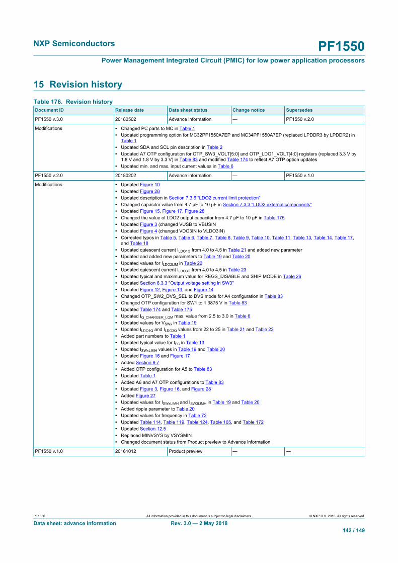
NXP Semiconductors PF1550Power Management Integrated Circuit (PMIC) for low power application processors
PF1550 All information provided in this document is subject to legal disclaimers. © NXP B.V. 2018. All rights reserved.
Data sheet: advance information Rev. 3.0 — 2 May 2018142 / 149
15 Revision historyTable 176. Revision historyDocument ID Release date Data sheet status Change notice Supersedes
PF1550 v.3.0 20180502 Advance information — PF1550 v.2.0
Modifications • Changed PC parts to MC in Table 1• Updated programming option for MC32PF1550A7EP and MC34PF1550A7EP (replaced LPDDR3 by LPDDR2) in
Table 1• Updated SDA and SCL pin description in Table 2• Updated A7 OTP configuration for OTP_SW3_VOLT[5:0] and OTP_LDO1_VOLT[4:0] registers (replaced 3.3 V by
1.8 V and 1.8 V by 3.3 V) in Table 83 and modified Table 174 to reflect A7 OTP option updates• Updated min. and max. input current values in Table 6
PF1550 v.2.0 20180202 Advance information — PF1550 v.1.0
Modifications • Updated Figure 10• Updated Figure 28• Updated description in Section 7.3.6 "LDO2 current limit protection"• Changed capacitor value from 4.7 µF to 10 µF in Section 7.3.3 "LDO2 external components"• Updated Figure 15, Figure 17, Figure 28• Changed the value of LDO2 output capacitor from 4.7 µF to 10 µF in Table 175• Updated Figure 3 (changed VUSB to VBUSIN• Updated Figure 4 (changed VDO3IN to VLDO3IN)• Corrected typos in Table 5, Table 6, Table 7, Table 8, Table 9, Table 10, Table 11, Table 13, Table 14, Table 17,
and Table 18• Updated quiescent current ILDO1Q from 4.0 to 4.5 in Table 21 and added new parameter• Updated and added new parameters to Table 19 and Table 20• Updated values for ILDO2LIM in Table 22• Updated quiescent current ILDO3Q from 4.0 to 4.5 in Table 23• Updated typical and maximum value for REGS_DISABLE and SHIP MODE in Table 26• Updated Section 6.3.3 "Output voltage setting in SW3"• Updated Figure 12, Figure 13, and Figure 14• Changed OTP_SW2_DVS_SEL to DVS mode for A4 configuration in Table 83• Changed OTP configuration for SW1 to 1.3875 V in Table 83• Updated Table 174 and Table 175• Updated IQ_CHARGER_LQM max. value from 2.5 to 3.0 in Table 6• Updated values for VSWx in Table 19• Updated ILDO1Q and ILDO3Q values from 22 to 25 in Table 21 and Table 23• Added part numbers to Table 1• Updated typical value for tFC in Table 13• Updated ISWxLIMH values in Table 19 and Table 20• Updated Figure 16 and Figure 17• Added Section 9.7• Added OTP configuration for A5 to Table 83• Updated Table 1• Added A6 and A7 OTP configurations to Table 83• Updated Figure 3, Figure 16, and Figure 28• Added Figure 27• Updated values for ISWxLIMH and ISW3LIMH in Table 19 and Table 20• Added ripple parameter to Table 20• Updated values for frequency in Table 72• Updated Table 114, Table 119, Table 124, Table 165, and Table 172• Updated Section 12.5• Replaced MINVSYS by VSYSMIN• Changed document status from Product preview to Advance information
PF1550 v.1.0 20161012 Product preview — —

NXP Semiconductors PF1550Power Management Integrated Circuit (PMIC) for low power application processors
PF1550 All information provided in this document is subject to legal disclaimers. © NXP B.V. 2018. All rights reserved.
Data sheet: advance information Rev. 3.0 — 2 May 2018143 / 149
16 Legal information
16.1 Data sheet status
Document status[1][2] Product status[3] Definition
[short] Data sheet: product preview Development This document contains certain information on a product under development.NXP reserves the right to change or discontinue this product without notice.
[short] Data sheet: advance information Qualification This document contains information on a new product. Specifications andinformation herein are subject to change without notice.
[short] Data sheet: technical data Production This document contains the product specification. NXP Semiconductorsreserves the right to change the detail specifications as may be required topermit improvements in the design of its products.
[1] Please consult the most recently issued document before initiating or completing a design.[2] The term 'short data sheet' is explained in section "Definitions".[3] The product status of device(s) described in this document may have changed since this document was published and may differ in case of multiple
devices. The latest product status information is available on the Internet at URL http://www.nxp.com.
16.2 DefinitionsDraft — The document is a draft version only. The content is still underinternal review and subject to formal approval, which may result inmodifications or additions. NXP Semiconductors does not give anyrepresentations or warranties as to the accuracy or completeness ofinformation included herein and shall have no liability for the consequencesof use of such information.
Short data sheet — A short data sheet is an extract from a full data sheetwith the same product type number(s) and title. A short data sheet isintended for quick reference only and should not be relied upon to containdetailed and full information. For detailed and full information see therelevant full data sheet, which is available on request via the local NXPSemiconductors sales office. In case of any inconsistency or conflict with theshort data sheet, the full data sheet shall prevail.
Product specification — The information and data provided in atechnical data data sheet shall define the specification of the product asagreed between NXP Semiconductors and its customer, unless NXPSemiconductors and customer have explicitly agreed otherwise in writing.In no event however, shall an agreement be valid in which the NXPSemiconductors product is deemed to offer functions and qualities beyondthose described in the technical data data sheet.
16.3 DisclaimersLimited warranty and liability — Information in this document is believedto be accurate and reliable. However, NXP Semiconductors does notgive any representations or warranties, expressed or implied, as to theaccuracy or completeness of such information and shall have no liabilityfor the consequences of use of such information. NXP Semiconductorstakes no responsibility for the content in this document if provided by aninformation source outside of NXP Semiconductors. In no event shall NXPSemiconductors be liable for any indirect, incidental, punitive, special orconsequential damages (including - without limitation - lost profits, lostsavings, business interruption, costs related to the removal or replacementof any products or rework charges) whether or not such damages are basedon tort (including negligence), warranty, breach of contract or any otherlegal theory. Notwithstanding any damages that customer might incur forany reason whatsoever, NXP Semiconductors’ aggregate and cumulativeliability towards customer for the products described herein shall be limitedin accordance with the Terms and conditions of commercial sale of NXPSemiconductors.
Right to make changes — NXP Semiconductors reserves the right tomake changes to information published in this document, including without
limitation specifications and product descriptions, at any time and withoutnotice. This document supersedes and replaces all information supplied priorto the publication hereof.
Suitability for use — NXP Semiconductors products are not designed,authorized or warranted to be suitable for use in life support, life-critical orsafety-critical systems or equipment, nor in applications where failure ormalfunction of an NXP Semiconductors product can reasonably be expectedto result in personal injury, death or severe property or environmentaldamage. NXP Semiconductors and its suppliers accept no liability forinclusion and/or use of NXP Semiconductors products in such equipment orapplications and therefore such inclusion and/or use is at the customer’s ownrisk.
Applications — Applications that are described herein for any of theseproducts are for illustrative purposes only. NXP Semiconductors makesno representation or warranty that such applications will be suitablefor the specified use without further testing or modification. Customersare responsible for the design and operation of their applications andproducts using NXP Semiconductors products, and NXP Semiconductorsaccepts no liability for any assistance with applications or customer productdesign. It is customer’s sole responsibility to determine whether the NXPSemiconductors product is suitable and fit for the customer’s applicationsand products planned, as well as for the planned application and use ofcustomer’s third party customer(s). Customers should provide appropriatedesign and operating safeguards to minimize the risks associated withtheir applications and products. NXP Semiconductors does not accept anyliability related to any default, damage, costs or problem which is basedon any weakness or default in the customer’s applications or products, orthe application or use by customer’s third party customer(s). Customer isresponsible for doing all necessary testing for the customer’s applicationsand products using NXP Semiconductors products in order to avoid adefault of the applications and the products or of the application or use bycustomer’s third party customer(s). NXP does not accept any liability in thisrespect.
Limiting values — Stress above one or more limiting values (as defined inthe Absolute Maximum Ratings System of IEC 60134) will cause permanentdamage to the device. Limiting values are stress ratings only and (proper)operation of the device at these or any other conditions above thosegiven in the Recommended operating conditions section (if present) or theCharacteristics sections of this document is not warranted. Constant orrepeated exposure to limiting values will permanently and irreversibly affectthe quality and reliability of the device.
Terms and conditions of commercial sale — NXP Semiconductorsproducts are sold subject to the general terms and conditions of commercialsale, as published at http://www.nxp.com/profile/terms, unless otherwiseagreed in a valid written individual agreement. In case an individualagreement is concluded only the terms and conditions of the respectiveagreement shall apply. NXP Semiconductors hereby expressly objects to

NXP Semiconductors PF1550Power Management Integrated Circuit (PMIC) for low power application processors
PF1550 All information provided in this document is subject to legal disclaimers. © NXP B.V. 2018. All rights reserved.
Data sheet: advance information Rev. 3.0 — 2 May 2018144 / 149
applying the customer’s general terms and conditions with regard to thepurchase of NXP Semiconductors products by customer.
No offer to sell or license — Nothing in this document may be interpretedor construed as an offer to sell products that is open for acceptance orthe grant, conveyance or implication of any license under any copyrights,patents or other industrial or intellectual property rights.
Export control — This document as well as the item(s) described hereinmay be subject to export control regulations. Export might require a priorauthorization from competent authorities.
Non-automotive qualified products — Unless this data sheet expresslystates that this specific NXP Semiconductors product is automotive qualified,the product is not suitable for automotive use. It is neither qualified nortested in accordance with automotive testing or application requirements.NXP Semiconductors accepts no liability for inclusion and/or use of non-automotive qualified products in automotive equipment or applications. Inthe event that customer uses the product for design-in and use in automotive
applications to automotive specifications and standards, customer (a) shalluse the product without NXP Semiconductors’ warranty of the product forsuch automotive applications, use and specifications, and (b) whenevercustomer uses the product for automotive applications beyond NXPSemiconductors’ specifications such use shall be solely at customer’s ownrisk, and (c) customer fully indemnifies NXP Semiconductors for any liability,damages or failed product claims resulting from customer design and useof the product for automotive applications beyond NXP Semiconductors’standard warranty and NXP Semiconductors’ product specifications.
Translations — A non-English (translated) version of a document is forreference only. The English version shall prevail in case of any discrepancybetween the translated and English versions.
16.4 TrademarksNotice: All referenced brands, product names, service names andtrademarks are the property of their respective owners.

NXP Semiconductors PF1550Power Management Integrated Circuit (PMIC) for low power application processors
PF1550 All information provided in this document is subject to legal disclaimers. © NXP B.V. 2018. All rights reserved.
Data sheet: advance information Rev. 3.0 — 2 May 2018145 / 149
TablesTab. 1. Orderable part variations ...................................6Tab. 2. Pin description ...................................................7Tab. 3. Thermal ratings ................................................. 8Tab. 4. Maximum ratings ...............................................9Tab. 5. Global conditions .............................................11Tab. 6. Input currents .................................................. 11Tab. 7. Internal 2.7 V Regulator (INT2P7) ...................12Tab. 8. Switch impedances and leakage currents ....... 12Tab. 9. Linear transients ..............................................13Tab. 10. Charger characteristics ................................... 13Tab. 11. Power-path management ................................ 14Tab. 12. Watchdog timer ............................................... 14Tab. 13. Charger timer .................................................. 14Tab. 14. Battery overcurrent protection ......................... 14Tab. 15. Thermal regulation .......................................... 15Tab. 16. Battery thermistor monitor ...............................15Tab. 17. USBPHY LDO ................................................. 15Tab. 18. LED characteristics ......................................... 16Tab. 19. SW1 and SW2 electrical characteristics ..........16Tab. 20. SW3 electrical characteristics ......................... 18Tab. 21. LDO1 electrical characteristics ........................19Tab. 22. LDO2 electrical characteristics ........................20Tab. 23. LDO3 electrical characteristics ........................20Tab. 24. VREFDDR electrical characteristics ................ 21Tab. 25. VSNVS electrical characteristics ..................... 22Tab. 26. IC level electrical characteristics ..................... 22Tab. 27. Voltage regulators ........................................... 23Tab. 28. SWx DVS setting selection ............................. 25Tab. 29. Buck regulator operating modes ..................... 26Tab. 30. Buck mode control .......................................... 27Tab. 31. SW1 and SW2 output voltage setting ..............28Tab. 32. Acceptable inductance and capacitance
values .............................................................. 31Tab. 33. Example inductor part numbers ...................... 31Tab. 34. Example capacitor part numbers .....................31Tab. 35. SW3 buck regulator operating modes ............. 32Tab. 36. SW3 buck mode control ..................................32Tab. 37. SW3 output voltage setting ............................. 33Tab. 38. Acceptable inductance and capacitance
values .............................................................. 34Tab. 39. Example inductor part numbers ...................... 34Tab. 40. Example capacitor part numbers .....................34Tab. 41. LDOy output voltage setting ............................36Tab. 42. LDOy control bits ............................................ 37Tab. 43. LDO2 output voltage setting ............................39Tab. 44. LDO2 control bits ............................................ 40Tab. 45. Battery regulation voltage register ...................44Tab. 46. VSYSMIN setting ............................................ 45Tab. 47. Charger current control register ...................... 49Tab. 48. Constant current charge settings .................... 49Tab. 49. Battery regulation voltage register ...................50Tab. 50. CV settings ......................................................51Tab. 51. Charger timers register ................................... 52Tab. 52. Fast charge timer settings ...............................52Tab. 53. Charger EOC configuration register ................ 53Tab. 54. EOC current thresholds ...................................54
Tab. 55. Charger timers register ................................... 54Tab. 56. EOC state timer settings ................................. 54Tab. 57. VBUS input current limit register ..................... 56Tab. 58. Input current limit settings ............................... 56Tab. 59. Thermal regulation .......................................... 58Tab. 60. Temperature regulation control register .......... 59Tab. 61. Thermal regulation settings .............................59Tab. 62. VBUS linear dynamic input voltage register .... 61Tab. 63. Input voltage regulation thresholds ................. 61Tab. 64. JEITA thermal control ......................................62Tab. 65. Temperature regulation control register .......... 62Tab. 66. JEITA temperature control register ................. 63Tab. 67. CV voltage adjustment settings .......................64Tab. 68. CC current adjustment settings .......................64Tab. 69. Battery overcurrent thresholds ........................ 66Tab. 70. LED modes ..................................................... 67Tab. 71. LED enable conditions .................................... 67Tab. 72. LED frequency setting .....................................68Tab. 73. PWRON pin OTP configuration options .......... 68Tab. 74. PWRON pin logic level ....................................68Tab. 75. PWRONDBNC settings ................................... 69Tab. 76. Standby pin polarity control .............................69Tab. 77. STANDBY pin logic level ................................ 69Tab. 78. WDI pin logic level .......................................... 70Tab. 79. ONKEY pin logic level .....................................71Tab. 80. ONKEYDBNC settings .................................... 71Tab. 81. State transition table ....................................... 75Tab. 82. A4 startup and power down sequence timing ...78Tab. 83. PF1550 start up configuration ......................... 78Tab. 84. Register DEVICE_ID - ADDR 0x00 .................80Tab. 85. Register OTP_FLAVOR - ADDR 0x01 ............ 80Tab. 86. Register SILICON_REV - ADDR 0x02 ............ 81Tab. 87. Register INT_CATEGORY - ADDR 0x06 ........ 81Tab. 88. Register SW_INT_STAT0 - ADDR 0x08 ......... 81Tab. 89. Register SW_INT_MASK0 - ADDR 0x09 ........ 82Tab. 90. Register SW_INT_SENSE0 - ADDR 0x0A ...... 82Tab. 91. Register SW_INT_STAT1 - ADDR 0x0B .........83Tab. 92. Register SW_INT_MASK1 - ADDR 0x0C ........83Tab. 93. Register SW_INT_SENSE1 - ADDR 0x0D ......83Tab. 94. Register SW_INT_STAT2 - ADDR 0x0E .........84Tab. 95. Register SW_INT_MASK2 - ADDR 0x0F ........ 84Tab. 96. Register SW_INT_SENSE2 - ADDR 0x10 ...... 84Tab. 97. Register LDO_INT_STAT0 - ADDR 0x18 ........85Tab. 98. Register LDO_INT_MASK0 - ADDR 0x19 .......85Tab. 99. Register LDO_INT_SENSE0 - ADDR 0x1A .... 85Tab. 100. Register TEMP_INT_STAT0 - ADDR 0x20 ..... 86Tab. 101. Register TEMP_INT_MASK0 - ADDR 0x21 .... 86Tab. 102. Register TEMP_INT_SENSE0 - ADDR 0x22 ...86Tab. 103. Register ONKEY_INT_STAT0 - ADDR 0x24 ... 87Tab. 104. Register ONKEY_INT_MASK0 - ADDR
0x25 .................................................................87Tab. 105. Register ONKEY_INT_SENSE0 - ADDR
0x26 .................................................................88Tab. 106. Register MISC_INT_STAT0 - ADDR 0x28 ...... 89Tab. 107. Register MISC_INT_MASK0- ADDR 0x29 ...... 89Tab. 108. Register MISC_INT_SENSE0 - ADDR 0x2A ... 90

NXP Semiconductors PF1550Power Management Integrated Circuit (PMIC) for low power application processors
PF1550 All information provided in this document is subject to legal disclaimers. © NXP B.V. 2018. All rights reserved.
Data sheet: advance information Rev. 3.0 — 2 May 2018146 / 149
Tab. 109. Register COINCELL_CONTROL - ADDR0x30 .................................................................90
Tab. 110. Register SW1_VOLT - ADDR 0x32 .................91Tab. 111. Register SW1_STBY_VOLT - ADDR 0x33 ......91Tab. 112. Register SW1_SLP_VOLT - ADDR 0x34 ........ 91Tab. 113. Register SW1_CTRL - ADDR 0x35 .................91Tab. 114. Register SW1_SLP_VOLT - ADDR 0x36 ........ 92Tab. 115. Register SW2_VOLT - ADDR 0x38 .................92Tab. 116. Register SW2_STBY_VOLT - ADDR 0x39 ......93Tab. 117. Register SW2_SLP_VOLT - ADDR 0x3A ........93Tab. 118. Register SW2_CTRL - ADDR 0x3B ................ 93Tab. 119. Register SW2_CTRL1 - ADDR 0x3C .............. 94Tab. 120. Register SW3_VOLT - ADDR 0x3E ................ 94Tab. 121. Register SW3_STBY_VOLT - ADDR 0x3F ..... 94Tab. 122. Register SW3_SLP_VOLT - ADDR 0x40 ........ 95Tab. 123. Register SW3_CTRL - ADDR 0x41 .................95Tab. 124. Register SW3_CTRL1 - ADDR 0x42 ...............95Tab. 125. Register VSNVS_CTRL - ADDR 0x48 ............ 96Tab. 126. Register VREFDDR_CTRL - ADDR 0x4A .......96Tab. 127. Register LDO1_VOLT - ADDR 0x4C .............. 96Tab. 128. Register LDO1_CTRL - ADDR 0x4D .............. 97Tab. 129. Register LDO2_VOLT - ADDR 0x4F ...............97Tab. 130. Register LDO2_CTRL - ADDR 0x50 ............... 97Tab. 131. Register LDO3_VOLT - ADDR 0x52 ............... 98Tab. 132. Register LDO3_CTRL - ADDR 0x53 ............... 98Tab. 133. Register PWRCTRL0 - ADDR 0x58 ................ 98Tab. 134. Register PWRCTRL1 - ADDR 0x59 ................ 99Tab. 135. Register PWRCTRL2 - ADDR 0x5A ................99Tab. 136. Register PWRCTRL3 - ADDR 0x5B ..............100Tab. 137. Register SW1_PWRDN_SEQ - ADDR 0x5F ..100Tab. 138. Register SW2_PWRDN_SEQ - ADDR 0x60 .. 101Tab. 139. Register SW2_PWRDN_SEQ - ADDR 0x61 .. 101Tab. 140. Register LDO1_PWRDN_SEQ - ADDR
0x62 ...............................................................102Tab. 141. Register LDO2_PWRDN_SEQ - ADDR
0x63 ...............................................................102Tab. 142. Register LDO3_PWRDN_SEQ - ADDR
0x64 ...............................................................103
Tab. 143. Register VREFDDR_PWRDN_SEQ - ADDR0x65 ...............................................................103
Tab. 144. Register STATE_INFO - ADDR 0x67 ............104Tab. 145. Register I2C_ADDR - ADDR 0x68 ................ 104Tab. 146. Register RC_16MHZ - ADDR 0x6B .............. 104Tab. 147. Register KEY1 - ADDR 0x6B ........................104Tab. 148. Register CHG_INT - ADDR 0x00 ..................105Tab. 149. Register CHG_INT_MASK - ADDR 0x02 ...... 105Tab. 150. Register CHG_INT_OK - ADDR 0x04 ........... 106Tab. 151. Register VBUS_SNS - ADDR 0x06 ...............107Tab. 152. Register CHG_SNS - ADDR 0x07 ................ 108Tab. 153. Register BATT_SNS - ADDR 0x08 ............... 109Tab. 154. Register CHG_OPER- ADDR 0x09 ...............109Tab. 155. Register CHG_TMR - ADDR 0x0A ................110Tab. 156. Register CHG_EOC_CNFG - ADDR 0x0D ....110Tab. 157. Register CHG_CURR_CNFG - ADDR 0x0E .. 111Tab. 158. Register BATT_REG - ADDR 0x0F ...............113Tab. 159. Register BATFET_CNFG - ADDR 0x11 ........ 114Tab. 160. Register THM_REG_CNFG - ADDR 0x12 .... 115Tab. 161. Register VBUS_INLIM_CNFG - ADDR 0x14 ..116Tab. 162. Register VBUS_LIN_DPM - ADDR 0x15 .......117Tab. 163. Register USB_PHY_LDO_CNFG - ADDR
0x16 ...............................................................117Tab. 164. Register DBNC_DELAY_TIME - ADDR
0x18 ...............................................................118Tab. 165. Register CHG_INT_CNFG - ADDR 0x19 ...... 118Tab. 166. Register THM_ADJ_SETTING - ADDR
0x1A .............................................................. 118Tab. 167. Register VBUS2SYS_CNFG - ADDR 0x1B ... 119Tab. 168. Register LED_PWM - ADDR 0x1C ............... 120Tab. 169. Register FAULT_BATFET_CNFG - ADDR
0x1D .............................................................. 120Tab. 170. Register LED_CNFG - ADDR 0x1E .............. 121Tab. 171. Register LED_CNFG - ADDR 0x1F .............. 122Tab. 172. Register PMIC bitmap ................................... 122Tab. 173. Register charger bitmap ................................126Tab. 174. Register OTP bitmap .....................................128Tab. 175. Bill of materials ..............................................134Tab. 176. Revision history .............................................142
FiguresFig. 1. Application diagram ...........................................3Fig. 2. Functional block diagram .................................. 4Fig. 3. Internal block diagram .......................................5Fig. 4. Pinout diagram .................................................. 6Fig. 5. SWx DVS transitions .......................................25Fig. 6. SWx DVS and non-DVS selection ...................26Fig. 7. SW3 block diagram .........................................31Fig. 8. LDOy Block Diagram .......................................36Fig. 9. LDO2 block diagram ....................................... 39Fig. 10. VREFDDR block diagram ............................... 41Fig. 11. VSNVS block diagram .....................................41Fig. 12. Battery charger internal block diagram ............42Fig. 13. Charger low battery (Startup sequence,
USB insert, VBATT = 0 V) .............................. 43Fig. 14. Charger healthy battery (Startup sequence,
USB insert, VBATT = 3.8 V) ........................... 44
Fig. 15. Input source detection delay ........................... 45Fig. 16. Charger state diagram .................................... 46Fig. 17. Charging profile ...............................................47Fig. 18. Thermal regulation .......................................... 57Fig. 19. Thermal regulation (Current versus Temp,
example with REGTEMP[1:0] = 00 andhysteresis ........................................................ 58
Fig. 20. Thermal regulation (Current, Temp versusTime, example with REGTEMP[1:0] = 00and hysteresis ................................................. 58
Fig. 21. Response to input voltage droop duringcharging ...........................................................60
Fig. 22. DPM function ...................................................61Fig. 23. CC charge current and CV charge voltage
adjustment .......................................................63Fig. 24. Response to battery overcurrent .....................66

NXP Semiconductors PF1550Power Management Integrated Circuit (PMIC) for low power application processors
PF1550 All information provided in this document is subject to legal disclaimers. © NXP B.V. 2018. All rights reserved.
Data sheet: advance information Rev. 3.0 — 2 May 2018147 / 149
Fig. 25. I2C sequence .................................................. 72Fig. 26. PMIC state machine ........................................72Fig. 27. A4 startup and power down sequence ............ 78Fig. 28. Typical Schematic ......................................... 133
Fig. 29. Recommended shielding for critical signals ... 136Fig. 30. Generic buck regulator architecture .............. 136Fig. 31. Layout example for buck regulators .............. 137Fig. 32. Package outline SOT1369-4 (QFN) .............. 139

NXP Semiconductors PF1550Power Management Integrated Circuit (PMIC) for low power application processors
PF1550 All information provided in this document is subject to legal disclaimers. © NXP B.V. 2018. All rights reserved.
Data sheet: advance information Rev. 3.0 — 2 May 2018148 / 149
Contents1 General description ............................................ 11.1 Features and benefits ........................................11.2 Applications ........................................................22 Application diagram ............................................32.1 Functional block diagram ...................................42.2 Internal block diagram ....................................... 53 Orderable parts ................................................... 54 Pinning information ............................................ 64.1 Pinning ...............................................................64.2 Pin definitions .................................................... 75 General product characteristics ........................ 85.1 Thermal characteristics ......................................85.2 Absolute maximum ratings ................................ 95.3 Electrical characteristics .................................. 115.3.1 Electrical characteristics – Battery charger ...... 115.3.2 Electrical characteristics – SW1 and SW2 .......165.3.3 Electrical characteristics – SW3 ...................... 185.3.4 Electrical characteristics – LDO1 .....................195.3.5 Electrical characteristics – LDO2 .....................195.3.6 Electrical characteristics – LDO3 .....................205.3.7 Electrical characteristics – VREFDDR ............. 215.3.8 Electrical characteristics – VSNVS .................. 215.3.9 Electrical characteristics – IC level bias
currents ............................................................226 Detailed description ..........................................236.1 Buck regulators ................................................246.2 SW1 and SW2 detailed description ................. 256.2.1 SWx dynamic voltage scaling description ........256.2.2 SWx DVS and non-DVS operation .................. 266.2.3 Regulator control ............................................. 266.2.4 Current limit protection .................................... 276.2.5 Output voltage setting in SWx ......................... 286.2.6 SWx external components ...............................316.3 SW3 detailed description .................................316.3.1 Regulator control ............................................. 326.3.2 Current limit protection .................................... 336.3.3 Output voltage setting in SW3 .........................336.3.4 SW3 external components .............................. 347 Low dropout linear regulators, VREFDDR
and VSNVS ........................................................ 347.1 General description ..........................................347.2 LDO1 and LDO3 detailed description .............. 357.2.1 Features summary ...........................................357.2.2 LDOy block diagram ........................................367.2.3 LDOy external components ............................. 367.2.4 LDOy output voltage setting ............................ 367.2.5 LDOy low power mode operation .................... 377.2.6 LDOy current limit protection ........................... 377.2.7 LDOy load switch mode .................................. 387.3 LDO2 detailed description ............................... 387.3.1 LDO2 features summary ................................. 387.3.2 LDO2 block diagram ........................................397.3.3 LDO2 external components .............................397.3.4 LDO2 output voltage setting ............................ 397.3.5 LDO2 Low-power mode operation ...................407.3.6 LDO2 current limit protection ...........................40
7.4 VREFDDR reference ....................................... 407.5 VSNVS LDO/Switch .........................................418 Battery charger description ............................. 428.1 Operating modes and behavioral description ... 438.2 Charger input source detection ....................... 458.3 Input self-discharge for reliable charger input
interrupt ............................................................458.4 Charger state diagram .....................................468.5 Charging profile ............................................... 478.5.1 Precharge state ............................................... 478.5.2 Fast charge constant current state .................. 488.5.3 Fast charge constant voltage state ..................508.5.4 End-of-charge state ......................................... 538.5.5 Done state ....................................................... 548.6 Battery supplement mode ................................558.7 Power path features ........................................ 558.7.1 VSYS regulation .............................................. 558.7.2 Input current limit .............................................558.7.3 Battery thermistor ............................................ 578.7.4 BATFET soft start ............................................578.8 Thermal ............................................................578.8.1 Thermal regulation ...........................................578.8.2 Thermal foldback ............................................. 598.8.3 Input voltage regulation mode ......................... 608.8.4 JEITA thermal control ......................................628.9 Fault states ...................................................... 648.9.1 Timer fault state ...............................................648.9.2 Watchdog timer state .......................................658.9.3 Thermal shutdown state .................................. 658.9.4 Battery overvoltage state .................................658.9.5 Charger fault priority ........................................658.9.6 Battery overcurrent limit ...................................668.10 LED indicator ................................................... 679 Control and interface signals .......................... 689.1 PWRON ........................................................... 689.2 STANDBY ........................................................ 699.3 RESETBMCU .................................................. 699.4 INTB .................................................................709.5 WDI ..................................................................709.6 ONKEY ............................................................ 709.7 Control interface I2C block description ............ 719.7.1 I2C device ID ...................................................719.7.2 I2C operation ................................................... 7110 PF1550 state machine ...................................... 7210.1 System ON states ........................................... 7310.1.1 Run state ......................................................... 7310.1.2 STANDBY state ...............................................7310.1.3 SLEEP state .................................................... 7410.2 System OFF states ..........................................7410.2.1 REGS_DISABLE ..............................................7410.2.2 CORE_OFF ..................................................... 7410.2.3 SHIP .................................................................7410.3 Turn on events ................................................ 7510.4 Turn off events ................................................ 7510.5 State diagram and transition conditions ...........7510.6 Regulator power-up sequencer ....................... 76

NXP Semiconductors PF1550Power Management Integrated Circuit (PMIC) for low power application processors
Please be aware that important notices concerning this document and the product(s)described herein, have been included in section 'Legal information'.
© NXP B.V. 2018. All rights reserved.For more information, please visit: http://www.nxp.comFor sales office addresses, please send an email to: [email protected]
Date of release: 2 May 2018
10.7 Regulator power-down sequencer ...................7711 Device start up ..................................................7711.1 Startup timing diagram .................................... 7711.2 Device start up configuration ........................... 7812 Register map ..................................................... 8012.1 Specific PMIC Registers (Offset is 0x00) .........8012.2 Specific Charger Registers (Offset is 0x80) ... 10512.3 Register PMIC bitmap ................................... 12212.4 Register charger bitmap ................................ 12612.5 Register OTP bitmap ..................................... 12813 Application details .......................................... 13213.1 Example schematic ........................................13213.2 Bill of materials .............................................. 13313.3 PF1550 layout guidelines .............................. 13413.3.1 General board recommendations .................. 13413.3.2 Component placement ...................................13513.3.3 General routing requirements ........................ 13513.3.4 Parallel routing requirements .........................13513.3.5 Switching regulator layout recommendations . 13613.4 Thermal information .......................................13713.4.1 Rating data .................................................... 13713.4.2 Estimation of junction temperature ................ 13714 Package outline ...............................................13815 Revision history .............................................. 14216 Legal information ............................................ 143