pf5020, power management integrated circuit (pmic) for ... · power management integrated circuit...
TRANSCRIPT
PF5020Power management integrated circuit (PMIC) for highperformance applicationsRev. 1 — 15 April 2020 Product data sheet
1 Overview
The PF5020 integrates multiple high performance buck regulators. It can operate as astand-alone point-of-load regulator IC, or as a companion chip to a larger PMIC.
Built-in one-time programmable (OTP) memory stores key startup configurations,drastically reducing external components typically used to set output voltage andsequence of regulators. Regulator parameters are adjustable through high-speed I2Cafter start up offering flexibility for different system states.
2 Features
• Three high efficiency buck converters• One linear regulator with load switch options• RTC supply and coin cell charger• Watchdog timer/monitor• Monitoring circuit to fit ASIL B safety level• One-time programmable device configuration• 3.4 MHz I2C communication interface• 40-pin QFN package with wettable flank and exposed pad

NXP Semiconductors PF5020Power management integrated circuit (PMIC) for high performance applications
PF5020 All information provided in this document is subject to legal disclaimers. © NXP B.V. 2020. All rights reserved.
Product data sheet Rev. 1 — 15 April 20202 / 105
3 Simplified application diagram
4
aaa-032546
V1P5DVINV1P5A
SW1FB
SW1LX
SW2FB
SW2LX
SWND1FB
SWND1LX
LDO1OUT
PGOOD
VDDIO
PGOODx
VDDIO4
INTB
AGND EP
VDDIO
SDA
TBBEN
VDDIO
XFAILB
V1P5A
RESETBMCU
VDDIO
PF5020
SW1INVPRE
SW2IN
SWND1IN
LDO1IN
VDDOTP
VDDIO
PWRON
STANDBY
ENxWDI
SCL
VDDIO
SYNC
Figure 1. Simplified application diagram
4 Ordering informationTable 1. Ordering information
PackageType number [1]
Name Description Version
MPF5020AMBA0ES [2]
MPF5020AMMA0ES [3]
Plastic thermal enhanced very thin quad flat pack; no leads, wettableflank, 40 terminals, 0.5 mm pitch, 6 mm x 6 mm x 0.85 mm bodyTemperature grade: 125
MPF5020AVNA0ES [4] HVQFN40Plastic thermal enhanced very thin quad flat pack; no leads, wettableflank, 40 terminals, 0.5 mm pitch, 6 mm x 6 mm x 0.85 mm bodyTemperature grade: 105
SOT618-14
[1] To order parts in tape and reel, add the R2 suffix to the part number.[2] Automotive part, Safety grade: ASIL B[3] Automotive part, Safety grade: QM[4] Industrial part

NXP Semiconductors PF5020Power management integrated circuit (PMIC) for high performance applications
PF5020 All information provided in this document is subject to legal disclaimers. © NXP B.V. 2020. All rights reserved.
Product data sheet Rev. 1 — 15 April 20203 / 105
5 Applications
• Automotive Infotainment• High-end consumer and industrial
6 Internal block diagram
aaa-029949
LDO
LDO10UT
SYNC
LDO1INDigital Signal(s)
Analog Reference(s)
20 MHz Clock/Derivative100 kHz Clock/Derivative
LDO VMON
AGND
VIN
VSNVS
V1P5D
VSNVS
VINOVLO
PGOODCONTROL
SW1VMON
SW2VMONSWND1VMON
LDOVMON
XFAILB
V1P5A
VBG2
VBG1
V1P5DLDO
V1P5ALDO
REGULATIONBANDGAP
BANDGAPCOMPARATOR
MONITORINGBANDGAP
PGOODMONITOR
RE
SETB
MC
U
WATCHDOGTIMER
DIGITAL COREAND
STATE MACHINE
THERMAL MONITORING/ SHUTDOWN
OTP MEMORY
WD monitoringP
GO
OD
1
EN1
PG
OO
D2
EN2
PG
OO
D3
EN3
PG
OO
D4
EN4
STA
ND
BY
PWR
ON
WD
I
INTB
VDD
OTP
TBBE
N
SC
L
VDD
IO
SDA
PGO
OD
VBG2
VBG1
VBG1
EPAD
SW1FB
SW1IN
SW1LX EAAND
DRIVER
REFSELEC.
VBG2
VBG1
SW1VMON
ABIST
ABIS
T
SW1 DVSAND MISC
REFERENCE
EPAD
SWND1FB
SWND1IN
SWND1LX EAAND
DRIVER
REFSELEC.
VBG2
VBG1
SWND1VMON
ABIST
SWND1 MISCREFERENCE
VTT
REF
ERE
NC
ESE
LEC
TOR
EPAD SW1FB/2
SW2FB
SW2IN
SW2LX EAAND
DRIVER
REFSELEC.
VBG2
SWD2VMON
SW2 DVSAND MISC
REFERENCE
ABIST
VBG1
VBG1
CLOCK MANAGEMENT(100 kHz / 20 MHz / PLL /
DIGITAL MODULE)
MANUAL TUNINGSPREAD SPECTRUMEXTERNAL CLOCK
SYNC
Figure 2. Internal block diagram

NXP Semiconductors PF5020Power management integrated circuit (PMIC) for high performance applications
PF5020 All information provided in this document is subject to legal disclaimers. © NXP B.V. 2020. All rights reserved.
Product data sheet Rev. 1 — 15 April 20204 / 105
7 Pinning information
7.1 Pinning
aaa-029951
SW1F
B40
EN2
39
EN1
38
RES
ETBM
CU
37
VDD
IO36
TBBE
N35
WD
I34
PGO
OD
433
PGO
OD
332
PWR
ON
31
SCL30
SDA29
VDDOTP28
SYNC27
PGOOD26
INTB25
V1P5D24
V1P5A23
STANDBY22
XFAILB21
SWN
D1F
B11
EN4
12
EN3
13
VSN
VS14
LDO
1OU
T15
LDO
1IN
16
VIN
17
AGN
D18
PGO
OD
119
PGO
OD
220
SW2FB 1
SW1IN 2
SW1LX 3
SW2LX 4
SW2IN 5
SWND1IN 6
SWND1LX
EPAD
7
NC1 8
NC2 9
NC3 10
Figure 3. Pin configuration for 40-pin QFN
7.2 Pin description
Table 2. Pin descriptionQFN pinnumber
Pin name Pin description Min Max Units
1 SW2FB Buck 2 output voltage feedback −0.3 6.0 V
2 SW1IN Buck 1 input supply −0.3 6.0 V
3 SW1LX Buck 1 switching node −0.3 6.0 V
4 SW2LX Buck 2 switching node −0.3 6.0 V
5 SW2IN Buck 2 input supply −0.3 6.0 V
6 SWND1IN Buck 3 input supply −0.3 6.0 V
7 SWND1LX Buck 3 switching node −0.3 6.0 V
8 NC1. not connected −0.3 6.0 V
9 NC2 not connected −0.3 6.0 V
10 NC3 not connected −0.3 6.0 V
11 SWND1FB Buck 3 output voltage feedback −0.3 6.0 V
12 EN4 LDO1 enable input −0.3 6.0 V
13 EN3 SWND1 enable input −0.3 6.0 V
14 VSNVS VSNVS regulator output −0.3 6.0 V

NXP Semiconductors PF5020Power management integrated circuit (PMIC) for high performance applications
PF5020 All information provided in this document is subject to legal disclaimers. © NXP B.V. 2020. All rights reserved.
Product data sheet Rev. 1 — 15 April 20205 / 105
QFN pinnumber
Pin name Pin description Min Max Units
15 LDO1OUT LDO1 output −0.3 6.0 V
16 LDO1IN LDO1 input supply −0.3 6.0 V
17 VIN Main input voltage −0.3 6.0 V
18 AGND Ground −0.3 0.3 V
19 PGOOD1 SW1 PGOOD output −0.3 6.0 V
20 PGOOD2 SW2 PGOOD output −0.3 6.0 V
21 XFAILB XFAILB input/output −0.3 6.0 V
22 STANDBY STANDBY signal input −0.3 6.0 V
23 V1P5A 1.6 V regulator output for internal analog −0.3 2 V
24 V1P5D 1.6 V regulator output for internal digital −0.3 2 V
25 INTB Interrupt open-drain output −0.3 6.0 V
26 PGOOD Global PGOOD output −0.3 6.0 V
27 SYNC External clock input/output for synchronization −0.3 6.0 V
28 VDDOTP Power supply for OTP programing block −0.3 10 V
29 SDA I2C SDA −0.3 6.0 V
30 SCL I2C SCL −0.3 6.0 V
31 PWRON PWRON input −0.3 6.0 V
32 PGOOD3 SWND1 PGOOD output −0.3 6.0 V
33 PGOOD4 LDO1 PGOOD output −0.3 6.0 V
34 WDI External watchdog reset input −0.3 6.0 V
35 TBBEN TBBEN mode control input −0.3 6.0 V
36 VDDIO I/O supply voltage. Connect to voltage rail at 1.8 V or 3.3V
−0.3 6.0 V
37 RESETBMCU RESETBMCU open-drain output −0.3 6.0 V
38 EN1 SW1 enable input −0.3 6.0 V
39 EN2 SW2 enable input −0.3 6.0 V
40 SW1FB Buck 1 output voltage feedback −0.3 6.0 V
41 EPAD Exposed pad. Connect to ground. −0.3 0.3 V
8 Absolute maximum ratingsTable 3. Absolute maximum ratingsSymbol Parameter Min Typ Max Unit
VIN Main input supply voltage [1] −0.3 — 6.0 V
SWxVIN,LDOxVIN
Regulator input supply voltage [1] −0.3 — 6.0 V
VDDOTP OTP programming input supply voltage −0.3 — 10 V
[1] Pin reliability may be affected if system voltages are above the maximum operating range of 5.5 V for extended period of time. To minimize systemreliability impact, system must not operate above 5.5 V for more than 1800 sec over the lifetime of the device.
NXP Semiconductors PF5020Power management integrated circuit (PMIC) for high performance applications
PF5020 All information provided in this document is subject to legal disclaimers. © NXP B.V. 2020. All rights reserved.
Product data sheet Rev. 1 — 15 April 20206 / 105
9 ESD ratingsTable 4. ESD ratingsAll ESD specifications are compliant with AEC-Q100 specification.
Symbol Parameter Min Typ Max Unit
VESD Human body model [1] — — 2000 V
VESD Charge device modelQFN package - all pins
[1] —
—
500
V
ILATCHUP Latch-up current — — 100 mA
[1] ESD testing is performed in accordance with the human body model (HBM) (CZAP = 100 pF, RZAP = 1500 Ω), and the charge device model (CDM),robotic (CZAP = 4.0 pF).
10 Thermal characteristicsTable 5. Thermal characteristicsSymbol Parameter Min Typ Max Unit
TA Ambient operating temperature −40 — 125 °C
TJ Junction temperature −40 — 150 °C
TST Storage temperature range −40 — 150 °C
TPPRT Peak package reflow temperature — — 260 °C
Table 6. QFN40 thermal resistance and package dissipation ratingsSymbol Parameter Typ Unit
RθJA Junction to Ambient Thermal ResistanceJESD51-7, 2s2p
[1] [2] [3] 32.6 °C/W
RθJA Junction to Ambient Thermal ResistanceJESD51-7, 2s6p
[1] [2] [4] 26.8 °C/W
ΨJT Junction to Top of Package Thermal ParameterJESD51-7, 2s2p
[1] [2] [3] 0.46 °C/W
ΨJT Junction to Top of Package Thermal ParameterJESD51-7, 2s6p
[1] [2] [4] 0.39 °C/W
[1] Determined in accordance to JEDEC JESD51-2A natural convection environment and uniform power.[2] Thermal resistance data in this report is solely for a thermal performance comparison of one package to another in a standardized specified environment.
It is not meant to predict the performance of a package in an application-specific environment.[3] Thermal test board meets JEDEC specification for this package (JESD51-7, 2s2p). PCB has a 3×3 array of thermal via under the exposed pad.[4] 2s6p PCB identical to 51-7 but with four additional internal layers at 35 µm thickness.
11 Operating conditionsTable 7. Operating conditionsSymbol Parameter Min Typ Max Unit
VIN Main input supply voltage UVDET — 5.5 V
NXP Semiconductors PF5020Power management integrated circuit (PMIC) for high performance applications
PF5020 All information provided in this document is subject to legal disclaimers. © NXP B.V. 2020. All rights reserved.
Product data sheet Rev. 1 — 15 April 20207 / 105
12 General description
12.1 FeaturesThe PF5020 is a power management integrated circuit (PMIC) designed to be theprimary power management building block for NXP high-end multimedia applicationprocessors from the i.MX 8 and S32V series. It is also capable of providing powersolution to the high end i.MX 6 series as well as several non-NXP processors.
• Buck regulators– SW1, SW2: 0.4 V to 1.8 V; 2500 mA; 2 % accuracy– SWND1; 1.0 V to 4.1 V; 2500 mA; 2 % accuracy– Dynamic voltage scaling on SW1 and SW2– SW1, SW2 configurable as a dual phase regulator– VTT termination mode on SW2– Programmable current limit– Spread-spectrum and manual tuning of switching frequency
• LDO regulator– LDO1, 1.5 V to 5.0 V, 400 mA: 3 % accuracy with optional load switch mode
• RTC LDO/switch supply from system supply– RTC supply VSNVS 1.8 V/3.0 V/3.3 V, 10 mA
• PGOOD output and monitor– Global PGOOD output and PGOOD monitor– Independent PGOOD output for each regulator
• Independent enable input for each regulator• Clock synchronization through configurable input/output sync pin• System features
– Fast PMIC startup– Advanced state machine for seamless processor interface– High speed I2C interface support (up to 3.4 MHz)– User programmable Standby and Off modes– Programmable soft start sequence and power down sequence– Programmable regulator configuration
• OTP (One-time programmable) memory for device configuration• Monitoring circuit to fit ASIL B safety level
– Independent voltage monitoring with programmable fault protection– Advance thermal monitoring and protection– External watchdog monitoring and programmable internal watchdog counter– I2C CRC and write protection mechanism– Analog built-in self-test (ABIST)
NXP Semiconductors PF5020Power management integrated circuit (PMIC) for high performance applications
PF5020 All information provided in this document is subject to legal disclaimers. © NXP B.V. 2020. All rights reserved.
Product data sheet Rev. 1 — 15 April 20208 / 105
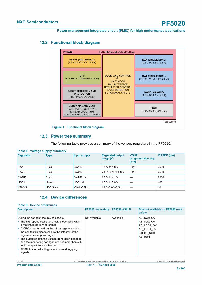
12.2 Functional block diagram
aaa-029952
PF5020 FUNCTIONAL BLOCK DIAGRAM
CLOCK MANAGEMENTEXTERNAL CLOCK SYNC
SPREAD SPECTRUMMANUAL FREQUENCY TUNING
VSNVS (RTC SUPPLY)(1.8 V/3.0 V/3.3 V, 10 mA)
LOGIC AND CONTROLI2C
WATCHDOGMCU INTERFACE
REGULATOR CONTROLFAULT DETECTION
FUNCTIONAL SAFETY
LDO1(1.5 V TO 5 V, 400 mA)
FAULT DETECTION ANDPROTECTION
(THERMAL/UV/OV/ILIM)
OTP(FLEXIBLE CONFIGURATION)
SW1 (SINGLE/DUAL)(0.4 V TO 1.8 V, 2.5 A)
SW2 (SINGLE/DUAL)(VTT/0.4 V TO 1.8 V, 2.5 A)
SWND1 (SINGLE)(1.0 V TO 4.1 V, 2.5 A)
Figure 4. Functional block diagram
12.3 Power tree summaryThe following table provides a summary of the voltage regulators in the PF5020.
Table 8. Voltage supply summaryRegulator Type Input supply Regulated output
range (V)VOUTprogrammable step(mV)
IRATED (mA)
SW1 Buck SW1IN 0.4 V to 1.8 V 6.25 2500
SW2 Buck SW2IN VTT/0.4 V to 1.8 V 6.25 2500
SWND1 Buck SWND1IN 1.0 V to 4.1 V — 2500
LDO1 Linear LDO1IN 1.5 V to 5.0 V — 400
VSNVS LDO/Switch VIN/LICELL 1.8 V/3.0 V/3.3 V — 10
12.4 Device differences
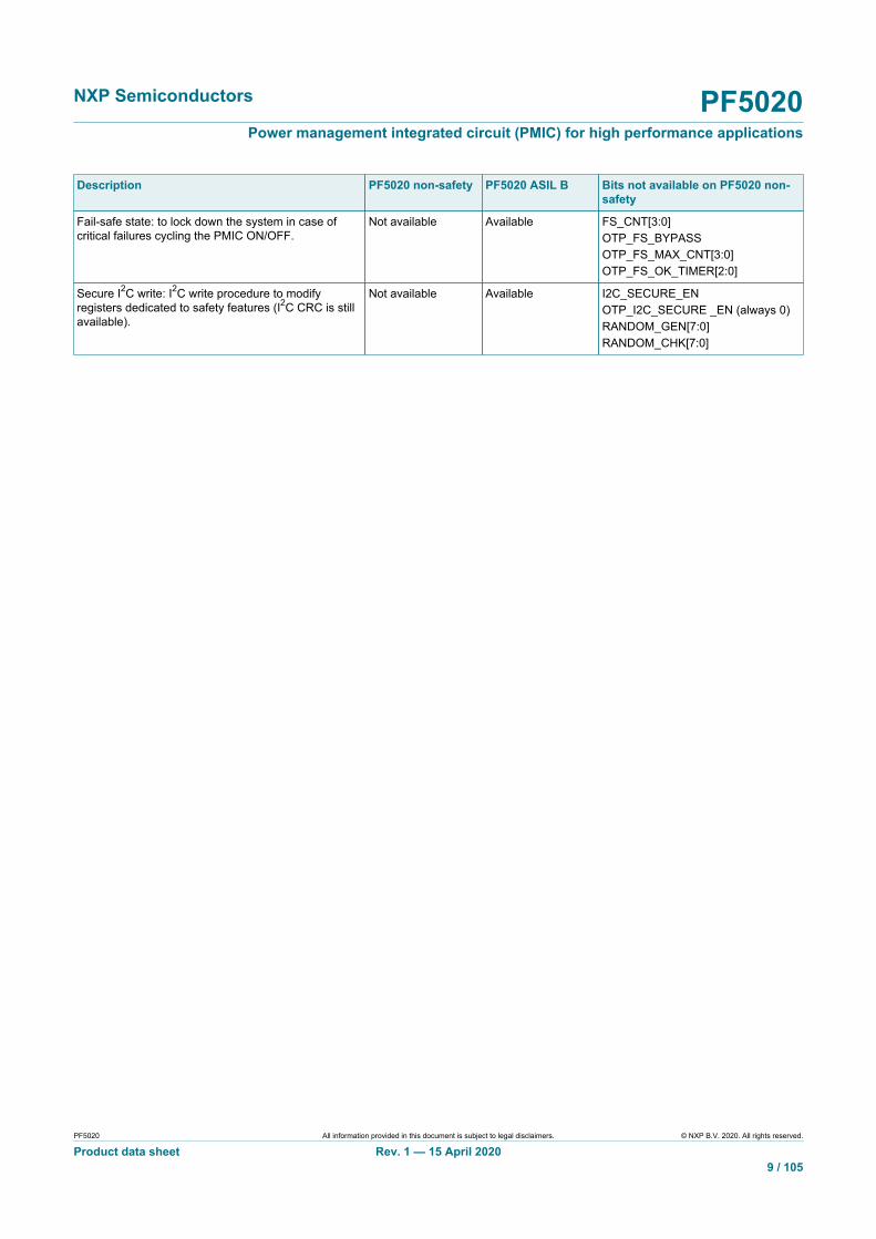
Table 9. Device differencesDescription PF5020 non-safety PF5020 ASIL B Bits not available on PF5020 non-
safety
During the self-test, the device checks:• The high speed oscillator circuit is operating within
a maximum of 15 % tolerance• A CRC is performed on the mirror registers during
the self-test routine to ensure the integrity of theregisters before powering up
• The output of both the voltage generation bandgapand the monitoring bandgap are not more than 5 %to 12 % apart from each other
• ABIST test on all voltage monitors and togglingsignals
Not available Available AB_SWx_OVAB_SWx_UVAB_LDO1_OVAB_LDO1_UVSTEST_NOKAB_RUN
NXP Semiconductors PF5020Power management integrated circuit (PMIC) for high performance applications
PF5020 All information provided in this document is subject to legal disclaimers. © NXP B.V. 2020. All rights reserved.
Product data sheet Rev. 1 — 15 April 20209 / 105
Description PF5020 non-safety PF5020 ASIL B Bits not available on PF5020 non-safety
Fail-safe state: to lock down the system in case ofcritical failures cycling the PMIC ON/OFF.
Not available Available FS_CNT[3:0]OTP_FS_BYPASSOTP_FS_MAX_CNT[3:0]OTP_FS_OK_TIMER[2:0]
Secure I2C write: I2C write procedure to modifyregisters dedicated to safety features (I2C CRC is stillavailable).
Not available Available I2C_SECURE_ENOTP_I2C_SECURE _EN (always 0)RANDOM_GEN[7:0]RANDOM_CHK[7:0]
NXP Semiconductors PF5020Power management integrated circuit (PMIC) for high performance applications
PF5020 All information provided in this document is subject to legal disclaimers. © NXP B.V. 2020. All rights reserved.
Product data sheet Rev. 1 — 15 April 202010 / 105
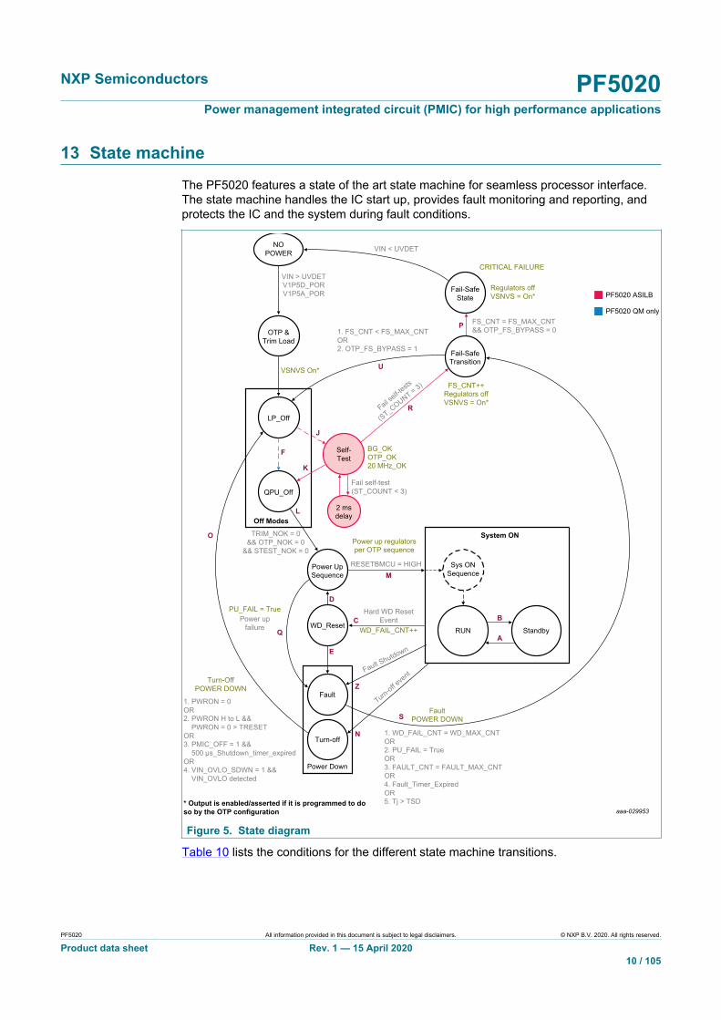
13 State machine
The PF5020 features a state of the art state machine for seamless processor interface.The state machine handles the IC start up, provides fault monitoring and reporting, andprotects the IC and the system during fault conditions.
aaa-029953
Fault
WD_Reset
D
Q
O
L
R
F
K
U
J
P
M
C
E
Z
N
SFault
POWER DOWN
Turn-OffPOWER DOWN
1. WD_FAIL_CNT = WD_MAX_CNTOR2. PU_FAIL = TrueOR3. FAULT_CNT = FAULT_MAX_CNTOR4. Fault_Timer_ExpiredOR5. Tj > TSD
1. PWRON = 0OR2. PWRON H to L && PWRON = 0 > TRESETOR3. PMIC_OFF = 1 && 500 µs_Shutdown_timer_expiredOR4. VIN_OVLO_SDWN = 1 && VIN_OVLO detected
* Output is enabled/asserted if it is programmed to doso by the OTP configuration
Turn-off
Power UpSequence
Off Modes
Hard WD ResetEvent
System ONPower up regulatorsper OTP sequence
PU_FAIL = TruePower up
failure
BG_OKOTP_OK20 MHz_OK
FS_CNT++Regulators offVSNVS = On*
Fail self-test(ST_COUNT < 3)
FS_CNT = FS_MAX_CNT&& OTP_FS_BYPASS = 01. FS_CNT < FS_MAX_CNT
OR2. OTP_FS_BYPASS = 1
Regulators offVSNVS = On*
TRIM_NOK = 0&& OTP_NOK = 0
&& STEST_NOK = 0
VIN > UVDETV1P5D_PORV1P5A_POR
VIN < UVDET
CRITICAL FAILURE
WD_FAIL_CNT++
RESETBMCU = HIGH Sys ONSequence
RUN
Fault Shutdown
Fail self-t
ests
(ST_COUNT = 3)
Turn-off e
vent
Standby
B
A
QPU_Off
LP_Off
Self-Test
2 msdelay
OTP &Trim Load
VSNVS On*
Fail-SafeState
Fail-SafeTransition
Power Down
NOPOWER
PF5020 ASILB
PF5020 QM only
Figure 5. State diagram
Table 10 lists the conditions for the different state machine transitions.

NXP Semiconductors PF5020Power management integrated circuit (PMIC) for high performance applications
PF5020 All information provided in this document is subject to legal disclaimers. © NXP B.V. 2020. All rights reserved.
Product data sheet Rev. 1 — 15 April 202011 / 105
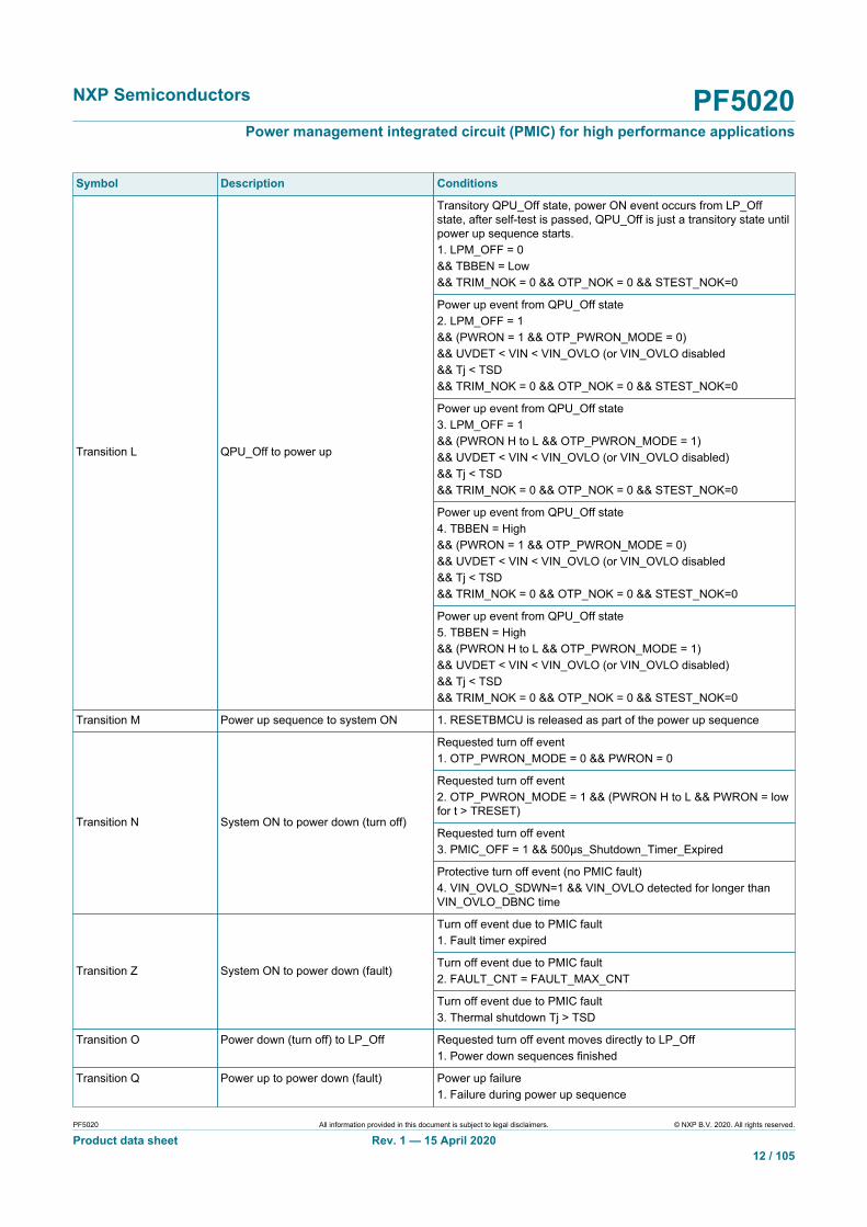
Table 10. State machine transition definitionSymbol Description Conditions
1. (STANDBY = 0 && STANDBYINV bit = 0)Transition A Standby to run
2. (STANDBY = 1 && STANDBYINV bit = 1)
1. (STANDBY = 1 && STANDBYINV bit = 0)Transition B Run to standby
2. (STANDBY = 0 && STANDBYINV bit = 1)
Transition C System ON to WD reset 1. Hard WD Reset event
Transition D WD reset to system ON 1. 30 µs delay passed && WD_EVENT_CNT < WD_MAX_CNT
Transition E WD reset to power down (fault) 1. WD_EVENT_CNT = WD_MAX_CNT
Transitory off state: device pass through LP_Off to self-test to QPU_Off (no power up event present)1. LPM_OFF = 1 && TBBEN = Low
Power up event from LP_Off state2. LPM_OFF = 0&& TBBEN = Low&& (PWRON = 1 && OTP_PWRON_MODE = 0)&& UVDET< VIN < VIN_OVLO (or VIN_OVLO disabled)&& Tj < TSD&& TRIM_NOK = 0 && OTP_NOK = 0
Power up event from LP_Off state3. LPM_OFF = 0&& TBBEN = Low&& (PWRON H to L && OTP_PWRON_MODE = 1&& UVDET < VIN < VIN_OVLO (or VIN_OVLO disabled)&& Tj < TSD&& TRIM_NOK = 0 && OTP_NOK = 0
Transition J LP_Off to self-test (PF5020 ASIL Bonly)
Conditions: Transitory OFF state to go into TBB mode. Device passthrough LP_Off to self-test to QPU_Off (no power up event present)4. TBBEN = high (V1P5D)
1. Pass self-testsTransition K Self-test to QPU_Off (PF5020 ASIL B
only) 2. TBBEN = high (V1P5D)
Transitory OFF state: device pass through LP_Off to QPU_Off (nopower up event present)1. LPM_OFF = 1&& TBBEN = Low
Power up event from LP_Off state2. LPM_OFF = 0&& TBBEN = Low&& (PWRON = 1 && OTP_PWRON_MODE = 0)&& UVDET< VIN < VIN_OVLO (or VIN_OVLO disabled)&& Tj < TSD&& TRIM_NOK = 0 && OTP_NOK = 0
Power up event from LP_Off state3. LPM_OFF =0&& TBBEN = Low&& (PWRON H to L && OTP_PWRON_MODE = 1)&& UVDET < VIN < VIN_OVLO (or VIN_OVLO disabled)&& Tj < TSD&& TRIM_NOK = 0 && OTP_NOK = 0
Transition F LP_Off to QPU_Off (PF5020 QM only)
Transitory OFF state: device pass through LP_Off to QPU_Off (nopower up event present)4. TBBEN = High (V1P5D)
NXP Semiconductors PF5020Power management integrated circuit (PMIC) for high performance applications
PF5020 All information provided in this document is subject to legal disclaimers. © NXP B.V. 2020. All rights reserved.
Product data sheet Rev. 1 — 15 April 202012 / 105
Symbol Description Conditions
Transitory QPU_Off state, power ON event occurs from LP_Offstate, after self-test is passed, QPU_Off is just a transitory state untilpower up sequence starts.1. LPM_OFF = 0&& TBBEN = Low&& TRIM_NOK = 0 && OTP_NOK = 0 && STEST_NOK=0
Power up event from QPU_Off state2. LPM_OFF = 1&& (PWRON = 1 && OTP_PWRON_MODE = 0)&& UVDET < VIN < VIN_OVLO (or VIN_OVLO disabled&& Tj < TSD&& TRIM_NOK = 0 && OTP_NOK = 0 && STEST_NOK=0
Power up event from QPU_Off state3. LPM_OFF = 1&& (PWRON H to L && OTP_PWRON_MODE = 1)&& UVDET < VIN < VIN_OVLO (or VIN_OVLO disabled)&& Tj < TSD&& TRIM_NOK = 0 && OTP_NOK = 0 && STEST_NOK=0
Power up event from QPU_Off state4. TBBEN = High&& (PWRON = 1 && OTP_PWRON_MODE = 0)&& UVDET < VIN < VIN_OVLO (or VIN_OVLO disabled&& Tj < TSD&& TRIM_NOK = 0 && OTP_NOK = 0 && STEST_NOK=0
Transition L QPU_Off to power up
Power up event from QPU_Off state5. TBBEN = High&& (PWRON H to L && OTP_PWRON_MODE = 1)&& UVDET < VIN < VIN_OVLO (or VIN_OVLO disabled)&& Tj < TSD&& TRIM_NOK = 0 && OTP_NOK = 0 && STEST_NOK=0
Transition M Power up sequence to system ON 1. RESETBMCU is released as part of the power up sequence
Requested turn off event1. OTP_PWRON_MODE = 0 && PWRON = 0
Requested turn off event2. OTP_PWRON_MODE = 1 && (PWRON H to L && PWRON = lowfor t > TRESET)
Requested turn off event3. PMIC_OFF = 1 && 500µs_Shutdown_Timer_Expired
Transition N System ON to power down (turn off)
Protective turn off event (no PMIC fault)4. VIN_OVLO_SDWN=1 && VIN_OVLO detected for longer thanVIN_OVLO_DBNC time
Turn off event due to PMIC fault1. Fault timer expired
Turn off event due to PMIC fault2. FAULT_CNT = FAULT_MAX_CNT
Transition Z System ON to power down (fault)
Turn off event due to PMIC fault3. Thermal shutdown Tj > TSD
Transition O Power down (turn off) to LP_Off Requested turn off event moves directly to LP_Off1. Power down sequences finished
Transition Q Power up to power down (fault) Power up failure1. Failure during power up sequence

NXP Semiconductors PF5020Power management integrated circuit (PMIC) for high performance applications
PF5020 All information provided in this document is subject to legal disclaimers. © NXP B.V. 2020. All rights reserved.
Product data sheet Rev. 1 — 15 April 202013 / 105
Symbol Description Conditions
Transition R Self-test to fail-safe transition 1. Self-tests fail 3 times&& TBBEN = low
Transition S Power down (fault) to fail-safe transition Turn off event due to a fault condition moves to fail-safe transition1. Power down sequence is finished
1. FS_CNT < FS_MAX_CNTTransition U Fail-safe transition to LP_Off
2. OTP_FS_BYPASS = 1
Transition P Fail-safe transition to fail-safe state(PF5020 ASILB only)
1. FS_CNT = FS_MAX_CNT&& OTP_FS_BYPASS = 0
13.1 State descriptions
13.1.1 OTP/TRIM load
Upon VIN application, the V1P5D and V1P5A regulators are turned on automatically.Once the V1P5D and V1P5A cross their respective POR thresholds, the fuses (for trimand OTP) are loaded into the mirror registers and into the functional I2C registers ifconfigured by the voltage on the VDDOTP pin.
The fuse circuits have a CRC error check routine which reports and protects againstregister loading errors on the mirror registers. If a register loading error is detected, thecorresponding TRIM_NOK or OTP_NOK flag is asserted. See Section 17 "OTP/TBB andhardwire default configurations" for details on handling fuse load errors.
If no fuse load errors are present, VSNVS is configured as indicated in the OTPconfiguration bits, and the state machine moves to the LP_off state.
13.1.2 LP_Off state
The LP_Off state is a low power off mode selectable by the LPM_OFF bit during thesystem On mode. By default, the LPM_OFF = 0 when VIN crosses the UVDET threshold,therefore the state machine stops at the LP_Off state until a valid power up eventis present. When LPM_OFF = 1, the state machine transitions automatically to theQPU_Off state if no power up event has been present and waits in the QPU_Off until avalid power up event is present.
The selection of the LPM_OFF bit is based on whether prioritizing low quiescent current(stay in the LP_Off state) or quick power up (move to the QPU_Off state).
If a power up event is started in LP_Off state with LPM_OFF = 0 and a fuse loading erroris detected, the PF5020 ignores the power up event and remains in the LP_Off state toavoid any potential damage to the system.
13.1.3 Self-test routine (PF5020 ASIL B only)
When the device transitions from the LP_Off state, it turns on all necessary internalcircuits as it moves into the self-test routine and performs a self-check routine to verifythe integrity of the internal circuits.
During the self-test routine the following blocks are verified:
• The high speed clock circuit is operating within a maximum of 15 % tolerance• The output of both the voltage generation bandgap and the monitoring bandgap are not
more than 5 % to 12 % apart from each other

NXP Semiconductors PF5020Power management integrated circuit (PMIC) for high performance applications
PF5020 All information provided in this document is subject to legal disclaimers. © NXP B.V. 2020. All rights reserved.
Product data sheet Rev. 1 — 15 April 202014 / 105
• A CRC is performed on the mirror registers during the self-test routine, to ensure theintegrity of the registers before powering up
• ABIST test on all voltage monitors.
To allow for varying settling times for the internal bandgap and clocks, the self-test blockis executed up to three times (with 2.0 ms between each test) if a failure is encountered,the state machine proceeds to the fail-safe transition.
A failure in the ABIST test is not interpreted as a self-test failure and it only sets thecorresponding ABIST flag for system information. The MCU is responsible for reading theinformation and deciding whether it can continue with a safe operation. See Section 18.1"System safety strategy" for the functional safety strategy of PF5020.
Upon a successful self-test, the state machine proceeds to the QPU_Off state.
13.1.4 QPU_Off state
The QPU_Off state is a higher power consumption Off mode, in which all internal circuitryrequired for a power on is biased and ready to start a power up sequence.
If LPM_OFF = 1 and no turn on event is present, the device stops at the QPU_Off state,and waits until a valid turn on event is present.
In this state, if VDDIO supply is provided externally, the device is able to communicatethrough I2C to access and modify the mirror registers in order to operate the device inTBB mode or to program the OTP registers as described in Section 17 "OTP/TBB andhardwire default configurations".
If a power up event is started and any of the TRIM_NOK, OTP_NOK or STEST_NOKflags are asserted, the device ignores the power up event and remains in the QPU_Offstate. See Section 17 "OTP/TBB and hardwire default configurations" for debugging afuse loading failure.
Upon a power up event, the default configuration from OTP or hardwire is loaded intotheir corresponding I2C functional register in the transition from QPU_Off to power upstate.
13.1.5 Power up sequence
During the power up sequence, the external regulators are turned on in a predefinedorder as programmed by the default (OTP or hardwire) sequence.
The RESETBMCU is also programmed as part of the power up sequence, and it is usedas the condition to enter the system On state. The RESETBMCU may be released in themiddle of the power up sequence, in this case, the remaining supplies in the power upcontinues to power up as the device is in the run state. See Section 14.5.2 "Power upsequencing" for details.
13.1.6 System On state
During the system On state, the MCU is powered and out of reset and the system is fullyoperational.
The system On is a virtual state composed by two modes of operations:
• Run state• Standby state

NXP Semiconductors PF5020Power management integrated circuit (PMIC) for high performance applications
PF5020 All information provided in this document is subject to legal disclaimers. © NXP B.V. 2020. All rights reserved.
Product data sheet Rev. 1 — 15 April 202015 / 105
Register to control the regulators output voltage, regulator enable, interrupt masks, andother miscellaneous functions can be written to or read from the functional I2C registermap during the system On state.
13.1.6.1 Run state
If the power up state is successfully completed, the state machine transitions to the runstate. In this state, RESETBMCU is released high, and the MCU is expected to boot upand set up specific registers on the PMIC as required during the system boot up process.
The Run mode is intended to be used as the normal mode of operation for the system.
Each regulator has specific registers to control its output voltage, operation mode and/orenable/disable state during the run state.
By default, the VSWx_RUN[7:0] / VLDOx_RUN[3:0] registers are loaded with the datastored in the OTP_VSWx[7:0] or OTP_VLDOx[3:0] bits respectively.
SWND1 uses only one global register to configure the output voltage during run orstandby mode. Upon power up, the VSWND1[4:0] bits are loaded with the values of theOTP_VSWND1[4:0].
Upon power up, if the switching regulator is part of the power up sequence, theSWx_RUN_MODE[1:0] bits will be loaded as needed by the system:
• When OTP_SYNC_MODE = 1, default SWx_RUN_MODE at power up is always set toPWM (0b01)
• When OTP_SYNC_MODE = 0 and OTP_SYNCOUT_EN = 1, defaultSWx_RUN_MODE at power up is always set to PWM (0b01)
• When OTP_FSS_EN = 1, default SWx_RUN_MODE at power up shall always set toPWM (0b01)
• If none of the above conditions are met, the default value of the SWx_RUN_MODE bitsat power up will be set by the OTP_SW_MODE bits.
When OTP_SW_MODE = 0, the default value of the SWx_RUN_MODE bits are set to0b11 (autoskip).
When OTP_SW_MODE = 1, the default value of the SWx_RUN_MODE bits are set to0b01 (PWM).
If the switching regulator is not part of the power up sequence, theSWx_RUN_MODE[1:0] bits are loaded with 0b00 (Off mode).
Likewise, if the LDO is part of the power up sequence, the LDOx_RUN_EN bit is set to1 (enabled) by default. If the LDO is not selected as part of the power up sequence, theLDOx_RUN_EN bit is set to 0 (disabled) by default.
In a typical system, each time the processor boots up (PMIC transitions from Off modeto run state), all output voltage configurations are reset to the default OTP configuration,and the MCU should configure the PMIC to its desired usage in the application.
13.1.6.2 Standby state
The standby state is intended to be used as a low power (state retention) mode ofoperation. In this state, the voltage regulators can be preset to a specific low powerconfiguration in order to reduce the power consumption during system’s sleep or stateretention modes of operations.

NXP Semiconductors PF5020Power management integrated circuit (PMIC) for high performance applications
PF5020 All information provided in this document is subject to legal disclaimers. © NXP B.V. 2020. All rights reserved.
Product data sheet Rev. 1 — 15 April 202016 / 105
The standby state is entered when the STANDBY pin is pulled high or low as definedby the STANBYINV bit. The STANDBY pin is pulled high/low by the MCU to enter/exitsystem low power mode. See Section 14.9.2 "STANDBY" for detailed configuration of theSTANDBY pin.
Each regulator has specific registers to control its output voltage, operation mode and/orenable/disable state during the standby state.
By default, the VSWx_STBY[7:0] / VLDOx_STBY[3:0] registers are loaded with the datastored in the OTP_VSWx[7:0] or OTP_VLDOx[3:0] bits respectively.
Upon power up, if the switching regulator is part of the power up sequence, theSWx_STBY_MODE[1:0] bits will be loaded as needed by the system:
• When OTP_SYNC_MODE = 1, default SWx_STBY_MODE at power up is always setto PWM (0b01)
• When OTP_SYNC_MODE = 0 and OTP_SYNCOUT_EN = 1, defaultSWx_STBY_MODE at power up is always set to PWM (0b01)
• When OTP_FSS_EN = 1, default SWx_STBY_MODE at power up shall always set toPWM (0b01)
• If none of the above conditions are met, the default value of the SWx_STBY_MODEbits at power up will be set by the OTP_SW_MODE bits.
When OTP_SW_MODE = 0, the default value of the SWx_STBY_MODE bits are set to0b11 (autoskip).
When OTP_SW_MODE = 1, the default value of the SWx_STBY_MODE bits are set to0b01 (PWM).
If the switching regulator is not part of the power up sequence, theSWx_STBY_MODE[1:0] bits are loaded with 0b00 (Off mode).
Likewise, if the LDO is part of the power up sequence, the LDOx_RUN_EN bit is set to1 (enabled) by default. If the LDO is not selected as part of the power up sequence, theLDOx_RUN_EN bit is set to 0 (disabled) by default.
Upon power up, the standby registers are loaded with the same default OTP values asthe run mode. The MCU is expected to program the desired standby values during bootup.
If any of the external regulators are disabled in the standby state, the power downsequencer is engaged as described in Section 14.6.2 "Power down sequencing".
13.1.7 WD_Reset
When a hard watchdog reset is present, the state machine increments theWD_EVENT_CNT[3:0] register and compares against the WD_MAX_CNT[3:0] register.If WD_EVENT_CNT[3:0] = WD_MAX_CNT[3:0], the state machine detects a cyclicwatchdog failure, it powers down the external regulators and proceeds to the fail-safetransition.
If WD_EVENT_CNT[3:0] < WD_MAX_CNT[3:0], the state machine performs a hard WDreset.
A hard WD reset can be generated from either a transition in the WDI pin or a WD eventinitiated by the internal watchdog counter as described in Section 15.10.2 "Watchdogreset behaviors".

NXP Semiconductors PF5020Power management integrated circuit (PMIC) for high performance applications
PF5020 All information provided in this document is subject to legal disclaimers. © NXP B.V. 2020. All rights reserved.
Product data sheet Rev. 1 — 15 April 202017 / 105
13.1.8 Power down state
During power down state, all regulators except VSNVS are disabled as configured inthe power down sequence. The power down sequence is programmable as defined inSection 14.6.2 "Power down sequencing".
Two types of events may lead to the power down sequence:
• Non faulty turn off events: move directly into LP_Off state as soon as power downsequence is finalized.
• Turn off events due to a PMIC fault: move to the fail-safe transition as soon as thepower down sequence is finalized.
13.1.9 Fail-safe transition
The fail-safe transition is entered if the PF5020 initiates a turn off event due to a PMICfault.
If the fail-safe transition is entered, the PF5020 provides four FAIL bits to indicate thesource of the failure:
• The PU_FAIL is set to 1 when the device shuts down due to a power up failure• The WD_FAIL is set to 1 when the device shuts down due to a watchdog event counter
max out• The REG_FAIL is set to 1 when the device shuts down due to a regulator failure (fault
counter maxed out or fault timer expired)• The TSD_FAIL is set to 1 when the device shuts down due to a thermal shutdown
The value of the FAIL bits is retained as long as VIN > UVDET.
The MCU can read the FAIL bits during the system On state in order to obtaininformation about the previous failure and can clear them by writing a 1 to them, providedthe state machine is able to power up successfully after such failure.
In the PF5020, when the state machine enters the fail-safe transition, a fail-safe counteris compared and increased, if the FS_CNT[3:0] reaches the maximum count, the devicecan be programmed to move directly to the fail-safe state to prevent a cyclic failure fromhappening.
13.1.10 Fail-safe state (PF5020 ASIL B only)
The fail-safe state works as a safety lock-down upon a critical device/system failure. It isreached when the FS_CNT [3:0] = FS_MAX_CNT [3:0].
A bit is provided to enable or disable the device to enter the fail-safe state upon a cyclicfailure. When the OTP_FS_BYPASS = 1, the fail-safe bypass operation is enabled andthe device always move to the LP_Off state, regardless of the value of the FS_CNT[3:0].If the OTP_FS_BYPASS = 0, the fail-safe bypass is disabled, and the device moves tothe fail-safe state when the proper condition is met.
The maximum number of times the device can pass through the fail-safetransition continuously prior to moving to a fail state is programmed by theOTP_FS_MAX_CNT[3:0] bits. If the FS_MAX_CNT[3:0] = 0x00, the device moves intothe fail-safe state as soon as it fails for the very first time.
The device can exit the fail-safe state only after a power cycle (VIN crossing UVDET)event is present.
NXP Semiconductors PF5020Power management integrated circuit (PMIC) for high performance applications
PF5020 All information provided in this document is subject to legal disclaimers. © NXP B.V. 2020. All rights reserved.
Product data sheet Rev. 1 — 15 April 202018 / 105
To avoid reaching the fail-safe state due to isolated fail-safe transition events,the FS_CNT [3:0] is gradually decreased based on a fail-safe OK timer. TheOTP_FS_OK_TIME[2:0] bits select the default time configuration for the fail-safe OKtimer between 1 to 60 min.
Table 11. Fail-safe OK timer configurationOTP_FS_OK_TIME[2:0] FS_CNT decrease period (min)
000 1
001 5
010 10
011 15
100 20
101 30
110 45
111 60
When the fail-safe OK timer reaches the configured time during the system On state, thestate machine decreases the FS_CNT[3:0] bits by one and starts a new count until theFS_CNT[3:0] is 0x00. The FS_CNT[3:0] may be manually cleared during the system Onstate if the system wants to control this counter manually.
14 General device operation
14.1 UVDETUVDET works as the main operation threshold for the PF5020. Crossing UVDET on therising edge is a mandatory condition for OTP fuses to be loaded into the mirror registersand allows the main PF5020 operation.
If VIN is below the UVDET threshold, the device remains in an unpowered state. A200 mV hysteresis is implemented on the UVDET comparator to set the falling threshold.
Table 12. UVDET thresholdSymbol Parameter Min Typ Max Unit
UVDET Rising UVDET 2.7 2.8 2.9 V
UVDET Falling UVDET 2.5 2.6 2.7 V
14.2 VIN OVLO conditionThe VIN_OVLO circuit monitors the main input supply of the PF5020. When this block isenabled, the PF5020 monitors its input voltage and can be programmed to react to anovervoltage in two ways:
• When the VIN_OVLO_SDWN = 0, the VIN_OVLO event triggers an OVLO interrupt butdoes not turn off the device
• When the VIN_OVLO_SDWN = 1, the VIN_OVLO event initiates a power downsequence
When the VIN_OVLO_EN = 0, the OVLO monitor is disabled and when theVIN_OVLO_EN = 1, the OVLO monitor is enabled. The default configuration of theVIN_OVLO_EN bit is set by the OTP_VIN_OVLO_EN bit in OTP. Likewise, the default
NXP Semiconductors PF5020Power management integrated circuit (PMIC) for high performance applications
PF5020 All information provided in this document is subject to legal disclaimers. © NXP B.V. 2020. All rights reserved.
Product data sheet Rev. 1 — 15 April 202019 / 105
value of the VIN_OVLO_SDWN bit is set by the OTP_VIN_OVLO_SDWN upon powerup.
During a power up transition, if the OTP_VIN_OVLO_SDWN = 0 the device allows theexternal regulators to come up and the PF5020 announces the VIN_OVLO conditionthrough an interrupt. If the OTP_VIN_OVLO_SDWN = 1, the device stops the power upsequence and returns to the corresponding Off mode.
Debounce on the VIN_OVLO comparator is programmable to 10 µs, 100 µs or 1.0 ms, bythe VIN_OVLO_DBNC[1:0] bits. The default value for the VIN_OVLO debounce is set bythe OTP_VIN_OVLO_DBNC[1:0] bits upon power up.
Table 13. VIN_OVLO debounce configurationVIN_OVLO_DBNC[1:0] VIN OVLO debounce value (µs)
00 10
01 100
10 1000
11 Reserved
Table 14. VIN_OVLO specificationsSymbol Parameter Min Typ Max Unit
VIN_OVLO VIN overvoltage lockout rising [1] 5.6 5.8 6.0 V
VIN_OVLO_HYS VIN overvoltage lockout hysteresis [1] — — 200 mV
[1] Operating the device above the maximum VIN = 5.5 V for extended period of time may degrade and cause permanentdamage to the device.
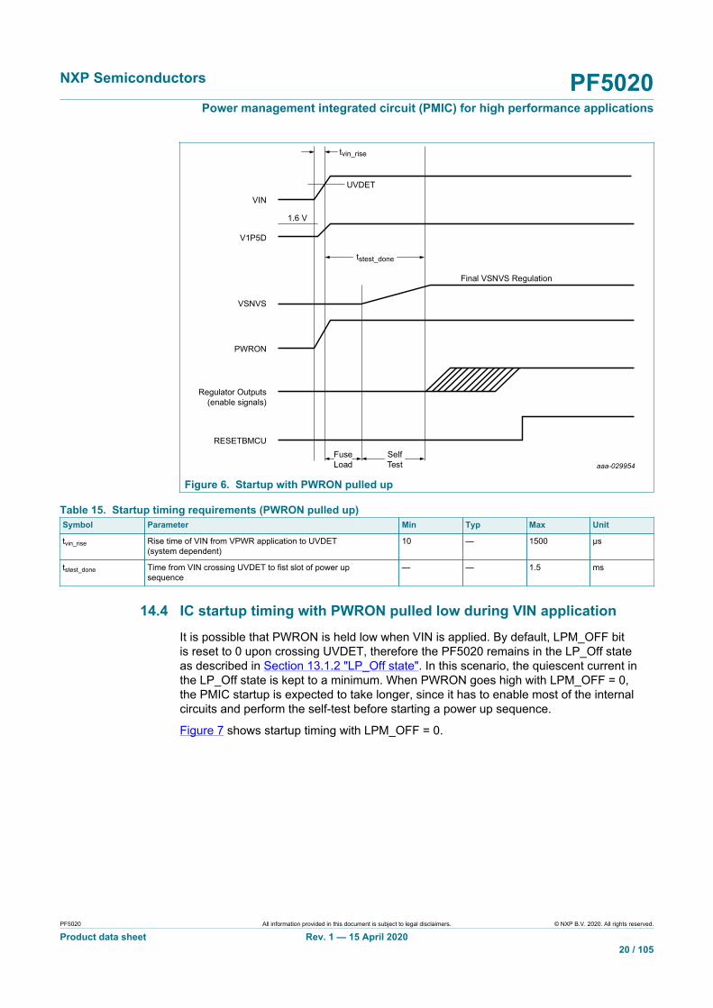
14.3 IC startup timing with PWRON pulled upThe PF5020 features a fast internal core power up sequence to fulfill system powerup timings of 5.0 ms or less, from power application until MCU is out of reset. Suchrequirement needs a maximum ramp up time of 1.5 ms for VIN to cross the UVDETthreshold in the rising edge.
A maximum core biasing time of 1.5 ms from VIN crossing to UVDET until the beginningof the power up sequence is ensured to allow up to 1.5 ms time frame for the voltageregulators power up sequence.
Timing for the external regulators to start up is programmed by default in the OTP fuses.
The 5.0 ms power up timing requirement is only applicable when the PWRON pinoperates in level sensitive mode OTP_PWRON_MODE = 0, however turn on timing isexpected to be the same for both level or edge sensitive modes after the power on eventis present.
In applications using the VSNVS regulator, if VSNVS is required to reach regulationbefore system regulators come up, the system should use the SEQ[7:0] bits to delay thesystem regulators to allow enough time for VSNVS to reach regulation before the powerup sequence is started.
NXP Semiconductors PF5020Power management integrated circuit (PMIC) for high performance applications
PF5020 All information provided in this document is subject to legal disclaimers. © NXP B.V. 2020. All rights reserved.
Product data sheet Rev. 1 — 15 April 202020 / 105
aaa-029954SelfTest
RESETBMCU
Regulator Outputs(enable signals)
PWRON
VSNVS
V1P5D
UVDET
VIN
FuseLoad
1.6 V
tstest_done
Final VSNVS Regulation
tvin_rise
Figure 6. Startup with PWRON pulled up
Table 15. Startup timing requirements (PWRON pulled up)Symbol Parameter Min Typ Max Unit
tvin_rise Rise time of VIN from VPWR application to UVDET(system dependent)
10 — 1500 µs
tstest_done Time from VIN crossing UVDET to fist slot of power upsequence
— — 1.5 ms
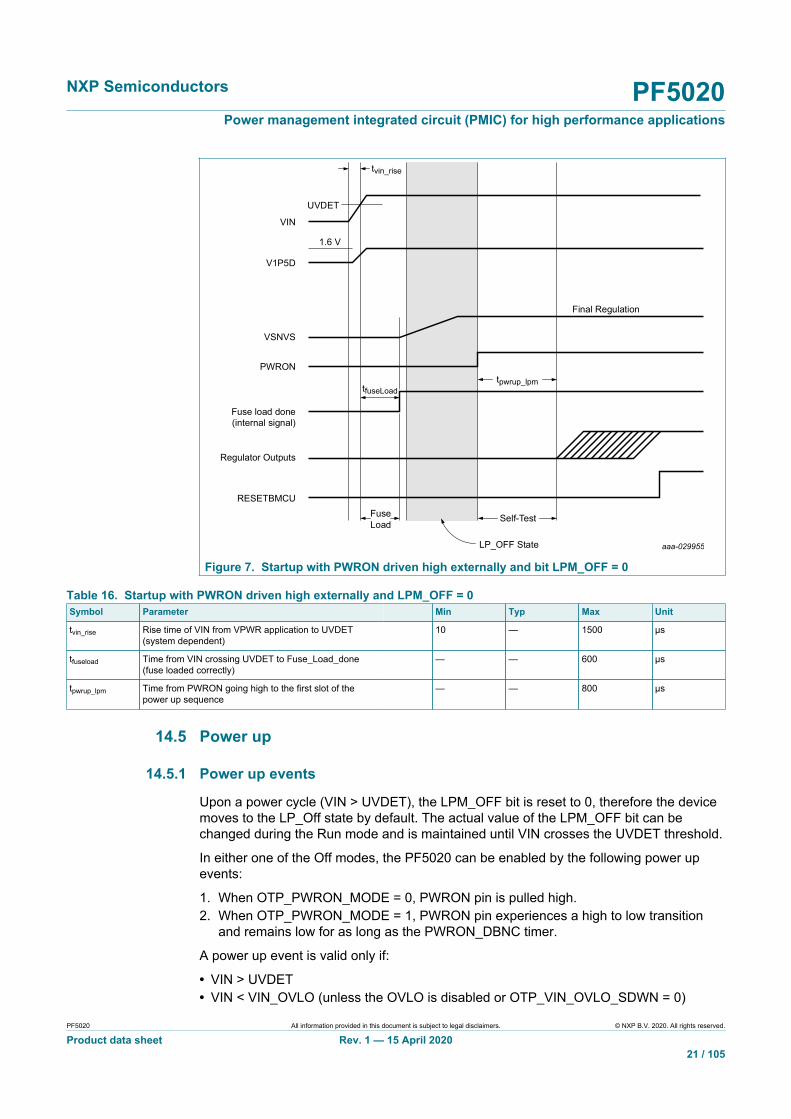
14.4 IC startup timing with PWRON pulled low during VIN applicationIt is possible that PWRON is held low when VIN is applied. By default, LPM_OFF bitis reset to 0 upon crossing UVDET, therefore the PF5020 remains in the LP_Off stateas described in Section 13.1.2 "LP_Off state". In this scenario, the quiescent current inthe LP_Off state is kept to a minimum. When PWRON goes high with LPM_OFF = 0,the PMIC startup is expected to take longer, since it has to enable most of the internalcircuits and perform the self-test before starting a power up sequence.
Figure 7 shows startup timing with LPM_OFF = 0.
NXP Semiconductors PF5020Power management integrated circuit (PMIC) for high performance applications
PF5020 All information provided in this document is subject to legal disclaimers. © NXP B.V. 2020. All rights reserved.
Product data sheet Rev. 1 — 15 April 202021 / 105
aaa-029955LP_OFF State
tpwrup_lpm
Self-Test
RESETBMCU
Regulator Outputs
Fuse load done(internal signal)
PWRON
VSNVS
V1P5D
UVDET
VIN
FuseLoad
tfuseLoad
1.6 V
Final Regulation
tvin_rise
Figure 7. Startup with PWRON driven high externally and bit LPM_OFF = 0
Table 16. Startup with PWRON driven high externally and LPM_OFF = 0Symbol Parameter Min Typ Max Unit
tvin_rise Rise time of VIN from VPWR application to UVDET(system dependent)
10 — 1500 µs
tfuseload Time from VIN crossing UVDET to Fuse_Load_done(fuse loaded correctly)
— — 600 µs
tpwrup_lpm Time from PWRON going high to the first slot of thepower up sequence
— — 800 µs
14.5 Power up
14.5.1 Power up events
Upon a power cycle (VIN > UVDET), the LPM_OFF bit is reset to 0, therefore the devicemoves to the LP_Off state by default. The actual value of the LPM_OFF bit can bechanged during the Run mode and is maintained until VIN crosses the UVDET threshold.
In either one of the Off modes, the PF5020 can be enabled by the following power upevents:
1. When OTP_PWRON_MODE = 0, PWRON pin is pulled high.2. When OTP_PWRON_MODE = 1, PWRON pin experiences a high to low transition
and remains low for as long as the PWRON_DBNC timer.
A power up event is valid only if:
• VIN > UVDET• VIN < VIN_OVLO (unless the OVLO is disabled or OTP_VIN_OVLO_SDWN = 0)
NXP Semiconductors PF5020Power management integrated circuit (PMIC) for high performance applications
PF5020 All information provided in this document is subject to legal disclaimers. © NXP B.V. 2020. All rights reserved.
Product data sheet Rev. 1 — 15 April 202022 / 105
• Tj < thermal shutdown threshold• TRIM_NOK = 0 && OTP_NOK = 0 && STEST_NOK = 0
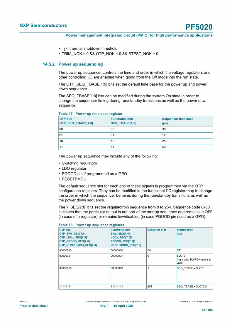
14.5.2 Power up sequencing
The power up sequencer controls the time and order in which the voltage regulators andother controlling I/O are enabled when going from the Off mode into the run state.
The OTP_SEQ_TBASE[1:0] bits set the default time base for the power up and powerdown sequencer.
The SEQ_TBASE[1:0] bits can be modified during the system On state in order tochange the sequencer timing during run/standby transitions as well as the power downsequence.
Table 17. Power up time base registerOTP bitsOTP_SEQ_TBASE[1:0]
Functional bitsSEQ_TBASE[1:0]
Sequencer time base(µs)
00 00 30
01 01 120
10 10 250
11 11 500
The power up sequence may include any of the following:
• Switching regulators• LDO regulator• PGOOD pin if programmed as a GPO• RESETBMCU
The default sequence slot for each one of these signals is programmed via the OTPconfiguration registers. They can be modified in the functional I2C register map to changethe order in which the sequencer behaves during the run/standby transitions as well asthe power down sequence.
The x_SEQ[7:0] bits set the regulator/pin sequence from 0 to 254. Sequence code 0x00indicates that the particular output is not part of the startup sequence and remains in OFF(in case of a regulator) or remains low/disabled (in case PGOOD pin used as a GPO).
Table 18. Power up sequence registersOTP bitsOTP_SWx_SEQ[7:0]/OTP_LDOx_SEQ[7:0]/OTP_PGOOD_SEQ[7:0]/OTP_RESETBMCU_SEQ[7:0]
Functional bitsSWx_SEQ[7:0]/LDOx_SEQ[7:0]/PGOOD_SEQ[7:0]/RESETBMCU_SEQ[7:0]
Sequence slot Startup time(µs)
00000000 00000000 Off Off
00000001 00000001 0 SLOT0(right after PWRON event isvalid)
00000010 00000010 1 SEQ_TBASE x SLOT1
.
.
.
.
.
.
.
.
.
.
.
.
11111111 11111111 254 SEQ_TBASE x SLOT254

NXP Semiconductors PF5020Power management integrated circuit (PMIC) for high performance applications
PF5020 All information provided in this document is subject to legal disclaimers. © NXP B.V. 2020. All rights reserved.
Product data sheet Rev. 1 — 15 April 202023 / 105
If RESETBMCU is not programmed in the OTP sequence, it will be enabled by defaultafter the last regulator programmed in the power up sequence.
When the _SEQ[7:0] bits of all regulators and PGOOD used as a GPIO are set to 0x00(OFF) and a power on event is present, the device moves to the run state in slave mode.In this mode, the device is enabled without any voltage regulator or GPO enabled. If theRESETBMCU is not programed in a power up sequence slot, it is released when thedevice enters the run state.
The slave mode is a special case of the power up sequence to address the scenariowhere the PF5020 is working as a slave PMIC, and supplies are meant to be enabledby the MCU during the system operation. In this scenario, if RESETBMCU is used, it isconnected to the master RESETBMCU pin.
Figure 8 provides an example of the power up/down sequence coming from the Offmodes.
aaa-032744
System On
End ofPWRUP
End ofPWRDN
Power down Seq.Run to Off
Power up Seq.Off to Run
INTB
SW2
SWND1
LDO1
SW1
RESETBMCU
Start ofPWRDN
Figure 8. Power up/down sequence between Off and system On state
When transitioning from Standby mode to Run mode, the power up sequencer isactivated only if any of the external regulators is re-enabled during this transition. If noneof the regulators toggle from Off to On and only voltage changes are being performedwhen entering or exiting Standby mode, the changes for the voltage regulators are madesimultaneously rather than going through the power up sequencer.
Figure 9 shows an example of the power up/down sequence when transitioning betweenRun and Standby modes.
NXP Semiconductors PF5020Power management integrated circuit (PMIC) for high performance applications
PF5020 All information provided in this document is subject to legal disclaimers. © NXP B.V. 2020. All rights reserved.
Product data sheet Rev. 1 — 15 April 202024 / 105
aaa-032746
PWRUP_lPWRDN_l
RunMode
STBYMode
PWRDN Sequencefrom Run to STBY
PWRUP Sequencefrom STBY to Run
INTB
RESETBMCU
SWND1
SW2
SW1
LDO1
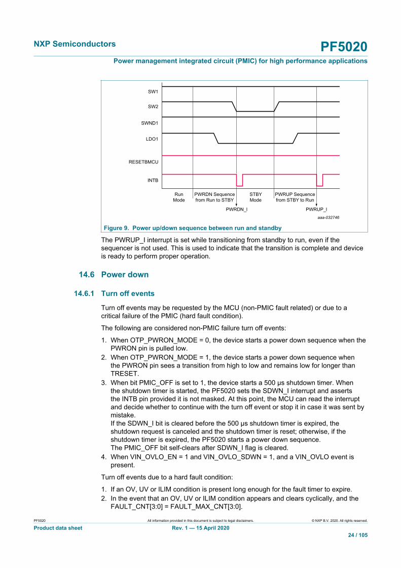
Figure 9. Power up/down sequence between run and standby
The PWRUP_I interrupt is set while transitioning from standby to run, even if thesequencer is not used. This is used to indicate that the transition is complete and deviceis ready to perform proper operation.
14.6 Power down
14.6.1 Turn off events
Turn off events may be requested by the MCU (non-PMIC fault related) or due to acritical failure of the PMIC (hard fault condition).
The following are considered non-PMIC failure turn off events:
1. When OTP_PWRON_MODE = 0, the device starts a power down sequence when thePWRON pin is pulled low.
2. When OTP_PWRON_MODE = 1, the device starts a power down sequence whenthe PWRON pin sees a transition from high to low and remains low for longer thanTRESET.
3. When bit PMIC_OFF is set to 1, the device starts a 500 µs shutdown timer. Whenthe shutdown timer is started, the PF5020 sets the SDWN_I interrupt and assertsthe INTB pin provided it is not masked. At this point, the MCU can read the interruptand decide whether to continue with the turn off event or stop it in case it was sent bymistake.If the SDWN_I bit is cleared before the 500 µs shutdown timer is expired, theshutdown request is canceled and the shutdown timer is reset; otherwise, if theshutdown timer is expired, the PF5020 starts a power down sequence.The PMIC_OFF bit self-clears after SDWN_I flag is cleared.
4. When VIN_OVLO_EN = 1 and VIN_OVLO_SDWN = 1, and a VIN_OVLO event ispresent.
Turn off events due to a hard fault condition:
1. If an OV, UV or ILIM condition is present long enough for the fault timer to expire.2. In the event that an OV, UV or ILIM condition appears and clears cyclically, and the
FAULT_CNT[3:0] = FAULT_MAX_CNT[3:0].
NXP Semiconductors PF5020Power management integrated circuit (PMIC) for high performance applications
PF5020 All information provided in this document is subject to legal disclaimers. © NXP B.V. 2020. All rights reserved.
Product data sheet Rev. 1 — 15 April 202025 / 105
3. If the watchdog fail counter is overflown, that is WD_EVENT_CNT = WD_MAX_CNT.4. When Tj crosses the thermal shutdown threshold as the temperature rises.
When the PF5020 experiences a turn off event due to a hard fault condition, the devicepass through the fail-safe transition after regulators have been powered down.
14.6.2 Power down sequencing
During a power down sequence, output voltage regulators can be turned off in twodifferent modes as defined by the PWRDWN_MODE bit.
1. When PWRDWN_MODE = 0, the regulators power down in sequential mode.2. When PWRDWN_MODE = 1, the regulators power down by groups.
During transition from run to standby, the power down sequencer is activated in thecorresponding mode, if any of the external regulators are turned off in the standbyconfiguration. If external regulators are not turned off during this transition, the powerdown sequencer is bypassed and the transition happens at once (any associated DVStransitions could still take time).
The PWRDN_I interrupt is set at the end of the transition from run to standby when thelast regulator has reached its final state, even if external regulators are not turned offduring this transition.
14.6.2.1 Sequential power down
When the device is set to the sequential power down, it uses the same _SEQ[7:0]registers as the power up sequence to power down in reverse order.
All regulators with the _SEQ[7:0] bits set to 0x00, power down immediately and theremaining regulators power down one OTP_SEQ_TBASE[1:0] delay after, in reverseorder as defined in the _SEQ[7:0] bits.
If PGOOD pin is used as a GPO, it is de-asserted as part of the power down sequenceas indicated by the PGOOD_SEQ[7:0] bits.
If the MCU requires a different power down sequence, it can change the values of theSEQ_TBASE[1:0] and the _SEQ[7:0] bits during the system On state.
When the state machine passes through any of the Off modes, the contents of theSEQ_TBASE[1:0] and _SEQ[7:0] bits are reloaded with the corresponding mirror register(OTP) values before it starts the next power up sequence.
14.6.2.2 Group power down
When the device is configured to power down in groups, the regulators are assigned to aspecific power down group. All regulators assigned to the same group are disabled at thesame time when the corresponding group is due to be disabled.
Power down groups shut down in decreasing order starting from the lowest hierarchygroup with a regulator shutting down (for instance Group 4 being the lowest hierarchyand Group 1 the highest hierarchy group). If no regulators are set to the lowest hierarchygroup, the power down sequence timer starts off the next available group that contains aregulator to power down.
Each regulator has its own _PDGRP[1:0] bits to set the power down group it belongs toas shown in Table 19.

NXP Semiconductors PF5020Power management integrated circuit (PMIC) for high performance applications
PF5020 All information provided in this document is subject to legal disclaimers. © NXP B.V. 2020. All rights reserved.
Product data sheet Rev. 1 — 15 April 202026 / 105
Table 19. Power down regulator group bitsOTP_SWx_PDGRP[1:0]OTP_LDO1_PDGRP[1:0]OTP_PGOOD_PDGRP[1:0]OTP_RESETBMCU_PDGRP[1:0]
SWx_PDGRP[1:0]LDO1_PDGRP[1:0]PGOOD_PDGRP[1:0]RESETBMCU_PDGRP[1:0]
Description
00 00 Regulator belongs to Group 4
01 01 Regulator belongs to Group 3
10 10 Regulator belongs to Group 2
11 11 Regulator belongs to Group 1
If PGOOD pin is used as a GPO, the PGOOD_PDGRP[1:0] is used to turn off thePGOOD pin in a specific group during the power down sequence. If PGOOD pin is usedin power good mode, it is recommended that the OTP_PGOOD_PDGRP bits are setto 11 to ensure the group power down sequencer does not detect these bits as part ofGroup 4.
Each one of power down groups have programmable time delay registers to set the timedelay after the regulators in this group have been turned off, and the next group can startto power down.
Table 20. Power down counter delayOTP bitsOTP_GRPx_DLY[1:0]
Functional bitsGRPx_DLY[1:0]
Power down delay(µs)
00 00 120
01 01 250
10 10 500
11 11 1000
If RESETBMCU is required to be asserted first before any of the external regulators fromthe corresponding group, the RESETBMCU_DLY provides a selectable delay to disablethe regulators after RESETBMCU is asserted.
Table 21. Programmable delay after RESETBMCU is assertedOTP bitsOTP_RESETBMCU_DLY[1:0]
Functional bitsRESETBMCU_DLY[1:0]
RESETBMCU delay(µs)
00 00 No delay
01 01 10
10 10 100
11 11 500
If RESETBMCU_DLY is set to 0x00, all regulators in the same power down group asRESETBMCU is disabled at the same time RESETBMCU is asserted.
Figure 10 shows an example of the power down sequence when PWRDWN_MODE = 1.

NXP Semiconductors PF5020Power management integrated circuit (PMIC) for high performance applications
PF5020 All information provided in this document is subject to legal disclaimers. © NXP B.V. 2020. All rights reserved.
Product data sheet Rev. 1 — 15 April 202027 / 105
aaa-029956
120 µsGRP3_DLY
120 µsGRP2_DLY
120 µsGRP1_DLY
PWR
DN
EVEN
TG
RP3
SDW
N
RES
ETBM
CU
asse
rted
GR
P1SD
WN
SUPP
LIES
End
ofPo
wer
Dow
n
GR
P2SD
WN
10 µs
PWRON
SWND1
SW2
RESETBMCU
SW1
LDO1
PDWN_GRP1GPR1_DLY = 120 µs
SW1LDO1
RESETBMCU_DLY = 10 µS
PDWN_GRP2GPR2_DLY = 120 µs
SW2
PDWN_GRP3GPR3_DLY = 120 µs
SWND1 NA
PDWN_GRP4
Figure 10. Group power down sequence example
14.6.2.3 Power down delay
After a power down sequence is started, the PWRON pin shall be masked until thesequence is finished and the programmable power down delay is reached. The devicecan power up again if a power up event is present. The power down delay time can beprogrammed on an OTP via the OTP_PD_SEQ_DLY[1:0] bits.
Table 22. Power down delay selectionOTP_PD_SEQ_DLY[1:0] Delay after power down sequence
00 No delay
01 1.5 ms
10 5.0 ms
11 10 ms

NXP Semiconductors PF5020Power management integrated circuit (PMIC) for high performance applications
PF5020 All information provided in this document is subject to legal disclaimers. © NXP B.V. 2020. All rights reserved.
Product data sheet Rev. 1 — 15 April 202028 / 105
aaa-029957Power Down
Sequence
Power DownDelay
RegulatorOutputs
VSNVS
RESETBMCU
PWRONShutdown
Event
OFF StateSystem OnState
Power DownSequence
Power Down Delay
Figure 11. Power down delay
The default value of the OTP_PD_SEQ_DLY[1:0] bits on an unprogrammed OTP deviceshall be 00.
14.7 Fault detectionThree types of faults are monitored per regulator: UV, OV and ILIM. Faults are monitoredduring power up sequence, run, standby and WD reset states. A fault event is notified tothe MCU through the INTB pin if the corresponding fault is not masked.
The fault configuration registers are reset to their default value after the power upsequences, and system must configure them as required during the boot-up process viaI2C commands.
For each type of fault, there is an I2C bit that is used to select whether the regulator iskept enabled or disabled when the corresponding regulator experience a fault event.
SWx_ILIM_STATE / LDOx_ILIM_STATE
• 0 = regulator disables upon an ILIM fault event• 1 = regulator remains on upon an ILIM fault event
SWx_OV_STATE / LDOx_OV_STATE
• 0 = regulator disables upon an OV fault event• 1 = regulator remains on upon an OV fault event
SWx_UV_STATE / LDOx_UV_STATE
• 0 = regulator disables upon an UV fault event• 1 = regulator remains on upon an UV fault event
The following table lists the functional bits associated with enabling/disabling the externalregulators when they experience a fault.

NXP Semiconductors PF5020Power management integrated circuit (PMIC) for high performance applications
PF5020 All information provided in this document is subject to legal disclaimers. © NXP B.V. 2020. All rights reserved.
Product data sheet Rev. 1 — 15 April 202029 / 105
Table 23. Regulator control during fault event bitsRegulator Bit to disable the
regulator during currentlimit
Bit to disable theregulator duringundervoltage
Bit to disable theregulator duringovervoltage
SW1 SW1_ILIM_STATE SW1_UV_STATE SW1_OV_STATE
SW2 SW2_ILIM_STATE SW2_UV_STATE SW2_OV_STATE
SWND1 SWND1_ILIM_STATE SWND1_UV_STATE SWND1_OV_STATE
LDO1 LDO1_ILIM_STATE LDO1_UV_STATE LDO1_OV_STATE
ILIM faults are debounced for 1.0 ms before they can be detected as a fault condition. Ifthe regulator is programed to disable upon an ILIM condition, the regulator turns off assoon as the ILIM condition is detected.
OV/UV faults are debounced for defined filter time before they are detected as a faultcondition. If the regulator is programmed to disable upon an OV or UV, the regulator willturn off if the fault persist for longer than 300 µs after the OV/UV fault has been detected.
RegX_STATE = 0 && Regx_FLT_REN = 0ILIM fault
RegX_STATE = 0 && Regx_FLT_REN = 0OV/UV fault
UserEnabled
300 µs
PGOOD
REGx
I_REGx
REGx_EN
RegX_PG
REGx_EN
REGx
UserEnabled
ILIM
1 ms aaa-028057
Figure 12. Regulator turned off upon with RegX_STATE = 0 and FLT_REN = 0
When a regulator is programmed to disable upon an OV, UV, or ILIM fault, a bit isprovided to decide whether a regulator can return to its previous configuration or remaindisabled when the fault condition is cleared.
SWx_FLT_REN / LDOx_FLT_REN
• 0 = regulator remains disabled after the fault condition is cleared or no longer present• 1 = regulator returns to its previous state if fault condition is cleared
If a regulator is programmed to remain disabled after clearing the fault condition, theMCU can turn it back ON during the system On state by toggling OFF and ON thecorresponding mode/enable bits.

NXP Semiconductors PF5020Power management integrated circuit (PMIC) for high performance applications
PF5020 All information provided in this document is subject to legal disclaimers. © NXP B.V. 2020. All rights reserved.
Product data sheet Rev. 1 — 15 April 202030 / 105
When the bit SWx_FLT_REN = 1, if a regulator is programmed to turn off upon an OV,UV or ILIM condition, the regulator returns to its previous state 500 µs after the faultcondition is cleared. If the regulator is programmed to turn off upon an ILIM condition, thedevice may take up to 1.0 ms to debounce the ILIM condition removal, in addition to the500 µs wait period to re-enable the regulator.
RegX_STATE = 0 && FLT_REN = 1ILIM fault
RegX_STATE = 0 && FLT_REN = 1OV/UV fault
REGx
I_REGx
REGx_EN
REGx
REGx_EN
PGOOD
REGx_PG
ILIM
1 ms 1.5 ms
500 µs300 µs
500 µs300 µs
1 ms 1.5 ms
aaa-028058
Figure 13. Regulator turned off upon with RegX_STATE = 0 and FLT_REN = 1
When any of the regulators is controlled by hardware using the ENx pins andprogrammed to turn off upon an OV, UV or ILIM fault, the _FLT_REN bit still controlswhether the regulator returns to its previous state or not regardless the state of the ENxpin.
To avoid fault cycling, a global fault counter is provided. Each time any of theexternal regulators encounter a fault event, the PF5020 compares the value of theFAULT_CNT[3:0] against the FAULT_MAX_CNT, and if it not equal, it increments theFAULT_CNT[3:0] and proceeds with the fault protection mechanism.
The processor is expected to read the counter value and reset it when the faults havebeen cleared and the device returns to a normal operation. If the processor does notreset the fault counter and it equals the FAULT_MAX_CNT[3:0] value, the state machineinitiates a power down sequence.
The default value of the FAULT_MAX_CNT[3:0] is loaded from theOTP_FAULT_MAX_CNT[3:0] bits during the power up sequence.
When the FAULT_MAX_CNT[3:0] is set to 0x00, the system disables the turn-off eventsdue to a fault counter maxing out.
When a regulator experiences a fault event, a fault timer is started. While this timeris in progress, the expectation is that the processor takes actions to clear the fault.For example, it could reduce its load in the event of a current limit fault, or turn off theregulator in the event of an overvoltage fault.
NXP Semiconductors PF5020Power management integrated circuit (PMIC) for high performance applications
PF5020 All information provided in this document is subject to legal disclaimers. © NXP B.V. 2020. All rights reserved.
Product data sheet Rev. 1 — 15 April 202031 / 105
If the fault clears before the timer expires, the state machine resumes the normaloperation, and the fault timer gets reset. If the fault does not clear before the timerexpires, a power down sequence is initiated to turn off the voltage regulators.
The default value of the fault timer is set by the OTP_TIMER_FAULT[3:0], however theduration of the fault timer can be changed during the system On state by modifying theTIMER_FAULT[3:0] bits in the I2C registers.
Table 24. Fault timer register configurationOTP bitsOTP_TIMER_FAULT [3:0]
Functional bitsTIMER_FAULT [3:0]
Timer value(ms)
0000 0000 1
0001 0001 2
0010 0010 4
0011 0011 8
0100 0100 16
0101 0101 32
0110 0110 64
0111 0111 128
1000 1000 256
1001 1001 512
1010 1010 1024
1011 1011 2056
1100 1100 Reserved
1101 1101 Reserved
1110 1110 Reserved
1111 1111 Disabled
Each voltage regulator has a dedicated I2C bit that is used to bypass the fault detectionmechanism for each specific fault.
SWx_ILIM_BYPASS / LDOx_ILIM_BYPASS
• 0 = ILIM protection enabled• 1 = ILIM fault bypassed
SWx_OV_BYPASS / LDOx_OV_BYPASS
• 0 = OV protection enabled• 1 = OV fault bypassed
SWx_UV_BYPASS / LDOx_UV_BYPASS
• 0 = UV protection enabled• 1 = UV fault bypassed
Table 25. Fault bypass bitsRegulator Bit to bypass a current
limitBit to bypass anundervoltage
Bit to bypass anovervoltage
SW1 SW1_ILIM_BYPASS SW1_UV_BYPASS SW1_OV_BYPASS
SW2 SW2_ILIM_BYPASS SW2_UV_BYPASS SW2_OV_BYPASS
SWND1 SWND1_ILIM_BYPASS SWND1_UV_BYPASS SWND1_OV_BYPASS

NXP Semiconductors PF5020Power management integrated circuit (PMIC) for high performance applications
PF5020 All information provided in this document is subject to legal disclaimers. © NXP B.V. 2020. All rights reserved.
Product data sheet Rev. 1 — 15 April 202032 / 105
Regulator Bit to bypass a currentlimit
Bit to bypass anundervoltage
Bit to bypass anovervoltage
LDO1 LDO1_ILIM_BYPASS LDO1_UV_BYPASS LDO1_OV_BYPASS
The default value of the OV_BYPASS, UV_BYPASS and ILIM_BYPASS bits upon powerup can be configured by their corresponding OTP bits.
Bypassing the fault detection prevents the specific fault from starting any of the protectivemechanism:
• Increment the counter• Start the fault timer• Disable the regulator if the corresponding _STATE bit is 0• OV/UV condition asserting the PGOOD and PGOODx pins low
When a fault is bypassed, the corresponding interrupt bit is still set and the INTB pin isasserted, provided the interrupt has not been masked.
14.7.1 Fault monitoring during power up state
An OTP bit is provided to select whether the output of the switching regulators isverified during the power up sequence and used as a gating condition to release theRESETBMCU or not.
• When OTP_PG_CHECK = 0, the output voltage of the regulators is not checked duringthe power up sequence and power good indication is not required to de-assert theRESETBMCU. In this scenario, the OV/UV monitors are masked until RESETBMCUis released; after this event, all regulators may start checking for faults after theircorresponding blanking period.
• When OTP_PG_CHECK = 1, the output voltage of the regulators is verified duringthe power up sequence and a power good condition is required to release theRESETBMCU.
When OTP_PG_CHECK = 1, OV and UV faults during the power up sequence arereported based on the internal PG (Power Good) signals of the corresponding externalregulator. The PGOOD pin can be used as an external indicator of an OV/UV failurewhen the RESETBMCU is ready to be de-asserted and it has been configured in thePGOOD mode. See Section 14.9.6 "PGOOD" for details on PGOOD pin operation andconfiguration.
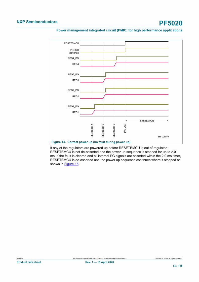
Regardless of the PGOOD pin configured as a power good indicator or not, the PF5020masks the detection of an OV/UV failure until RESETBMCU is ready to be released, atthis point the device checks for any OV/UV condition for the regulators turned on so far.If all regulators powered up before or in the same sequence slot than RESETBMCU arein regulation, RESETBMCU is de-asserted and the power up sequence can continue asshown in Figure 14.
NXP Semiconductors PF5020Power management integrated circuit (PMIC) for high performance applications
PF5020 All information provided in this document is subject to legal disclaimers. © NXP B.V. 2020. All rights reserved.
Product data sheet Rev. 1 — 15 April 202033 / 105
aaa-028059
RESETBMCU
REG4_PG
REG3_PG
REG2_PGSE
QSL
OT
1
SEQ
SLO
T2
SEQ
SLO
T3
SYSTEM ON
PG's
OK
REG4
REG3
REG2
REG1_PG
REG1
PGOOD(optional)
Figure 14. Correct power up (no fault during power up)
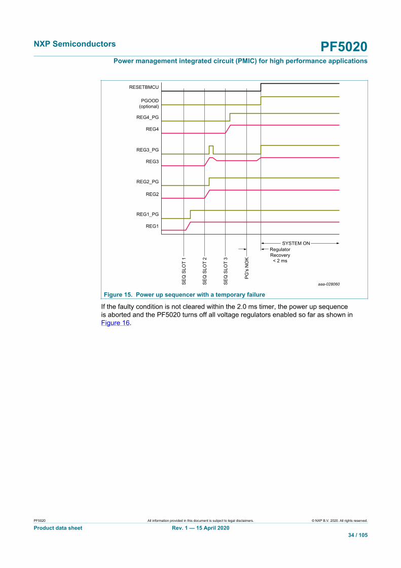
If any of the regulators are powered up before RESETBMCU is out of regulator,RESETBMCU is not de-asserted and the power up sequence is stopped for up to 2.0ms. If the fault is cleared and all internal PG signals are asserted within the 2.0 ms timer,RESETBMCU is de-asserted and the power up sequence continues where it stopped asshown in Figure 15.
NXP Semiconductors PF5020Power management integrated circuit (PMIC) for high performance applications
PF5020 All information provided in this document is subject to legal disclaimers. © NXP B.V. 2020. All rights reserved.
Product data sheet Rev. 1 — 15 April 202034 / 105
aaa-028060
RESETBMCU
REG4_PG
REG3_PG
REG2_PGSE
QSL
OT
1
SEQ
SLO
T2
SEQ
SLO
T3
SYSTEM ONRegulatorRecovery
< 2 ms
PG's
NO
K
REG4
REG3
REG2
REG1_PG
REG1
PGOOD(optional)
Figure 15. Power up sequencer with a temporary failure
If the faulty condition is not cleared within the 2.0 ms timer, the power up sequenceis aborted and the PF5020 turns off all voltage regulators enabled so far as shown inFigure 16.

NXP Semiconductors PF5020Power management integrated circuit (PMIC) for high performance applications
PF5020 All information provided in this document is subject to legal disclaimers. © NXP B.V. 2020. All rights reserved.
Product data sheet Rev. 1 — 15 April 202035 / 105
aaa-029987
RESETBMCU
PGOOD4
PGOOD3
PGOOD2SE
QSL
OT
1
SEQ
SLO
T2
SEQ
SLO
T3
PWR
UP
Fail
Reg Power down2 ms (max)Recovery
PG's
NO
K
REG4
REG3
REG2
PGOOD1
REG1
PGOOD
Figure 16. Power up sequencer aborted as fault persists for longer than 2.0 ms
Supplies enabled after RESETBMCU are checked for OV, UV and ILIM faults after eachof them are enabled. If an OV, UV or ILIM condition is present, the PF5020 starts a faultdetection and protection mechanism as described in Section 14.7 "Fault detection". Atthis point, the MCU should be able to read the interrupt and react upon a fault event asdefined by the system.
When OTP_PG_CHECK=1, If PGOOD is used as a GPIO, it may be released at any timein the power up sequence as long as the RESETBMCU is released after one or more ofthe SW regulators or LDO regulator.
If a regulator fault occurs after RESETBMCU is de-asserted but before the powerup sequence is finalized, the power up sequences continue to turn on the remainingregulators as configured, even if a fault detection mechanism is active on an earlierregulator.
14.8 Interrupt managementThe MCU is notified of any interrupt through the INTB pin and various interrupt registers.
The interrupt registers are composed by three types of bits to help manage all theinterrupt requests in the PF5020:
• The interrupt latch XXXX_I: this bit is set when the corresponding interrupt eventoccurs. It can be read at any time, and is cleared by writing a 1 to the bit.
• The mask bit XXXX_M: this bit controls whether a given interrupt latch pulls the INTBpin low or not.
• When the mask bit is 1, the interrupt latch does not control the INTB pin.

NXP Semiconductors PF5020Power management integrated circuit (PMIC) for high performance applications
PF5020 All information provided in this document is subject to legal disclaimers. © NXP B.V. 2020. All rights reserved.
Product data sheet Rev. 1 — 15 April 202036 / 105
• When the mask bit is 0, the INTB pin is pulled low as long as the corresponding latchbit is set.
• The sense bit XXXX_S: if available, the sense bit provides the actual status of thesignal triggering the interrupt.
The INTB pin is a reflection of an “OR” logic of all the interrupt status bits which controlthe pin.
Interrupts are stored in two levels on the interrupts registers. At first level, the SYS_INTregister provides information about the Interrupt register that originated the interruptevent.
The corresponding SYS_INT bits is set as long as the INTB pin is programmed to assertwith any of the interrupt bits of the respective interrupt registers.
• STATUS1_I: this bit is set when the interrupt is generated within the INT STATUS1register
• STATUS2_I: this bit is set when the interrupt is generated within the INT STATUS2register
• MODE_I: this bit is set when the interrupt is generated within the SW MODE INTregister
• ILIM_I: this bit is set when the interrupt is generated within any of the SW ILIM INT orLDO ILIM INT registers
• UV_I: this bit is set when the interrupt is generated within any of the SW UV INT orLDO UV INT registers
• OV_I: this bit is set when the interrupt is generated within any of the SW OV INT orLDO OV INT registers
• PWRON_I: this bit is set when the interrupt is generated within the PWRON INTregister
• EWARN_I: is set when an early warning event occurs to indicate an imminentshutdown
The SYS_INT bits are set when the INTB pin is asserted by any of the second levelinterrupt bits that have not been masked in their corresponding mask registers. Whenthe second level interrupt bit is cleared, the corresponding first level interrupt bit on theSYS_INT register will be cleared automatically.
The INTB pin will remain asserted if any of the first level interrupts bit is set, and it will bede-asserted only when all the unmasked second level interrupts are cleared and thus allthe first level interrupts are cleared as well.
At second level the remaining registers provide the exact source for the interrupt event.
Table 26 shows a summary of the interrupt latch, mask and sense pins available on thePF5020.
Table 26. Interrupt registersRegister name BIT7 BIT6 BIT5 BIT4 BIT3 BIT2 BIT1 BIT0
INT STATUS1 SDWN_I FREQ_RDY_I CRC_I PWRUP_I PWRDN_I — PGOOD_I VIN_OVLO_I
INT MASK1 SDWN_M FREQ_RDY_M CRC_M PWRUP_M PWRDN_M — PGOOD_M VIN_OVLO_M
INT SENSE1 — — — — — — PGOOD_S VIN_OVLO_S
THERM INT WDI_I FSYNC_FLT_I THERM_155_I THERM_140_I THERM_125_I THERM_110_I THERM_95_I THERM_80_I
THERM MASK WDI_M FSYNC_FLT_M THERM_155_M THERM_140_M THERM_125_M THERM_110_M THERM_95_M THERM_80_M
THERM SENSE WDI_S FSYNC_FLT_S THERM_155_S THERM_140_S THERM_125_S THERM_110_S THERM_95_S THERM_80_S
SW MODE INT — SWND1_MODE_I — — — — SW2_MODE_I SW1_MODE_I
SW MODE MASK — SWND1_MODE_M — — — — SW2_MODE_M SW1_MODE_M
SW ILIM INT — SWND1_ILIM_I — — — — SW2_ILIM_I SW1_ILIM_I
SW ILIM MASK — SWND1_ILIM_M — — — — SW2_ILIM_M SW1_ILIM_M

NXP Semiconductors PF5020Power management integrated circuit (PMIC) for high performance applications
PF5020 All information provided in this document is subject to legal disclaimers. © NXP B.V. 2020. All rights reserved.
Product data sheet Rev. 1 — 15 April 202037 / 105
Register name BIT7 BIT6 BIT5 BIT4 BIT3 BIT2 BIT1 BIT0
SW ILIM SENSE — SWND1_ILIM_S — — — — SW2_ILIM_S SW1_ILIM_S
LDO ILIM INT — — — — — — — LDO1_ILIM_I
LDO ILIM MASK — — — — — — — LDO1_ILIM_M
LDO ILIM SENSE — — — — — — — LDO1_ILIM_S
SW UV INT — SWND1_UV_I — — — — SW2_UV_I SW1_UV_I
SW UV MASK — SWND1_UV_M — — — — SW2_UV_M SW1_UV_M
SW UV SENSE — SWND1_UV_S — — — — SW2_UV_S SW1_UV_S
SW OV INT — SWND1_OV_I — — — — SW2_OV_I SW1_OV_I
SW OV MASK — SWND1_OV_M — — — — SW2_OV_M SW1_OV_M
SW OV SENSE — SWND1_OV_S — — — — SW2_OV_S SW1_OV_S
LDO UV INT — — — — — — — LDO1_UV_I
LDO UV MASK — — — — — — — LDO1_UV_M
LDO UV SENSE — — — — — — — LDO1_UV_S
LDO OV INT — — — — — — — LDO1_OV_I
LDO OV MASK — — — — — — — LDO1_OV_M
LDO OV SENSE — — — — — — — LDO1_OV_S
PWRON INT BGMON_I PWRON_8S_I PWRON_4S_I PRON_3S_I PWRON_2S_I PWRON_1S_I PWRON_REL_I PWRON_PUSH_I
PWRON MASK BGMON_M PWRON_8S_M PWRON_4S_M PRON_3S_M PWRON_2S_M PWRON_1S_M PWRON_REL_M PWRON_PUSH_M
PWRON SENSE BGMON_S — — — — — — PWRON_S
EN_SENSE — — — — EN4_S EN3_S EN2_S EN1_S
SYS INT EWARN_I PWRON_I OV_I UV_I ILIM_I MODE_I STATUS2_I STATUS1_I
14.9 I/O interface pinsThe PF5020 PMIC is fully programmable via the I2C interface. Additional communicationbetween MCU, PF5020 and other companion PMIC is provided by direct logic interfacingincluding INTB, RESETBMCU, PGOOD, among other pins.
aaa-029988
PM
IC_O
N_R
EQ
PM
IC_S
TBY
_RE
Q
PWR
ON
STA
ND
BY
WD
OG
_BW
DI
i.MX8 MCU
PMIC1PF5020
PMIC2PF5020
VDDIO
RES
ETB
MC
UP
OR
_B
VDDIO VDDIO VDDIO
INTB
PGO
OD
PWR
ON
PG
OO
D1
INT_
B
GP
IOE
N4
GP
IOE
N3
GP
IO
GP
IO
GP
IO
VDDIO VDDIO
PG
OO
D
PGO
OD
1
XFAI
LB
GP
IO
GP
IO
EN
2
GP
IOE
N4
STAN
DBY
RE
SETB
MC
U
INTB WD
I
XFA
ILB
GP
IOE
N3
GP
IOE
N2
V1P5A
Figure 17. I/O interface diagram
NXP Semiconductors PF5020Power management integrated circuit (PMIC) for high performance applications
PF5020 All information provided in this document is subject to legal disclaimers. © NXP B.V. 2020. All rights reserved.
Product data sheet Rev. 1 — 15 April 202038 / 105
Table 27. I/O electrical specificationsSymbol Parameter Min Typ Max Unit
PWRON_VIL PWRON low input voltage — — 0.4 V
PWRON_VIH PWRON high input voltage 1.4 — 5.5 V
STANDBY_VIL STANDBY low input voltage — — 0.4 V
STANDBY_VIH STANDBY high input voltage 1.4 — 5.5 V
RESETBMCU_VOL RESETBMCU low output voltage−2.0 mA load current
0
—
0.4
V
INTB_VOL INTB low output voltage−2.0 mA load current
0
—
0.4
V
ENx_VIL ENx low input voltage — — 0.4 V
ENx_VIH ENx high input voltage 1.4 — 5.5 V
WDI_VIL WDI low input voltage — — 0.3*VDDIO V
WDI_VIH WDI high input voltage 0.7*VDDIO — 5.5 V
RWDI_PD WDI internal pull-down resistance 0.475 1.0 — MΩ
PGOOD_VOL PGOOD low output voltage−2.0 mA load current
0
—
0.4
V
PGOODx_VOL PGOODx low output voltage−2.0 mA load current
0
—
0.4
V
TBBEN_VIL TBBEN low input voltage — — 0.4 V
TBBEN_VIH TBBEN high input voltage 1.4 — 5.5 V
RTBBEN_PD TBBEN internal pull-down resistance 0.475 1.0 — MΩ
XFAILB_VIL XFAILB low input voltage — — 0.4 V
XFAILB_VIH XFAILB high input voltage 1.4 — 5.5 V
XFAILB_VOH XFAILB high output voltagePulled-up to V1P5A
V1P5A − 0.5
—
—
V
XFAILB_VOL XFAILB low output voltage−2.0 mA load current
0
—
0.4
V
SCL_VIL SCL low input voltage — — 0.3*VDDIO V
SCL_VIH SCL high input voltage 0.7*VDDIO — VDDIO V
SDA_VIL SDA low input voltage — — 0.3*VDDIO V
SDA_VIH SDA high input voltage 0.7*VDDIO — VDDIO V
SDA_VOL SDA low output voltage−20 mA load current
0
—
0.4
V
14.9.1 PWRON
PWRON is an input signal to the IC that acts as a power up event signal in the PF5020.
The PWRON pin has two modes of operation as programed by theOTP_PWRON_MODE bit.
When OTP_PWRON_MODE = 0, the PWRON pin operates in level sensitive mode. Inthis mode, the device is in the corresponding off mode when the PWRON pin is pulledlow. Pulling the PWRON pin high is a necessary condition to generate a power on event.
PWRON may be pulled up to VSNVS or VIN with an external 100 kΩ resistor if device isintended to come up automatically with VIN application. See Section 14.5 "Power up" fordetails on power up requirements.
When OTP_PWRON_MODE = 1, the PWRON pin operates in edge sensitive mode. Inthis mode, PWRON is used as an input from a push button connected to the PMIC.
NXP Semiconductors PF5020Power management integrated circuit (PMIC) for high performance applications
PF5020 All information provided in this document is subject to legal disclaimers. © NXP B.V. 2020. All rights reserved.
Product data sheet Rev. 1 — 15 April 202039 / 105
When the switch is not pressed, the PWRON pin is pulled up to VIN externally througha 100 kΩ resistor. When the switch is pressed, the PWRON pin should be shorted toground. The PWRON_S bit is low whenever the PWRON pin is at logic 0 and is highwhenever the PWRON pin is at logic 1.
The PWRON pin has a programmable debounce on the rising and falling edges asshown in Table 28.
Table 28. PWRON debounce configuration in edge detection modeBits Value Falling edge debounce
(ms)Rising edge debounce(ms)
PWRON_DBNC[1:0] 00 32 32
PWRON_DBNC[1:0] 01 32 32
PWRON_DBNC[1:0] 10 125 32
PWRON_DBNC[1:0] 11 750 32
The default value for the power on debounce is set by the OTP_PWRON_DBNC[1:0]bits.
Pressing the PWRON switch for longer than the debounce time starts a power onevent as well as generate interrupts which the processor may use to initiate PMIC statetransitions.
During the system On state, when the PWRON button is pushed (logic 0) for longer thanthe debounce setting, the PWRON_PUSH_I interrupt is generated. When the PWRONbutton is released (logic 1) for longer than the debounce setting, the PWRON_REL_Iinterrupt is generated.
The PWRON_1S_I, PWRON_2S_I, PWRON_3S_I, PWRON_4S_I and PWRON_8S_Iinterrupts are generated when the PWRON pin is held low for longer than 1, 2, 3, 4 and 8seconds respectively.
If PWRON_RST_EN = 1, pressing the PWRON for longer than the delay programmed byTRESET[1:0] forces a PMIC reset. A PMIC reset initiates a power down sequence, waitfor 30 µs to allow all supplies to discharge and then it powers back up with the defaultOTP configuration.
If PWRON_RST_EN = 0, the device starts a turn off event after push button is pressedfor longer than TRESET[1:0].
Table 29. TRESET configurationTRESET[1:0] Time to reset
00 2 s
01 4 s
10 8 s
11 16 s
The default value of the TRESET delay is programmable through the OTP_TRESET[1:0]bits.
14.9.2 STANDBY
STANDBY is an input signal to the IC, when this pin is asserted, the device enters thestandby mode and when de-asserted, the part exits Standby mode.
NXP Semiconductors PF5020Power management integrated circuit (PMIC) for high performance applications
PF5020 All information provided in this document is subject to legal disclaimers. © NXP B.V. 2020. All rights reserved.
Product data sheet Rev. 1 — 15 April 202040 / 105
STANDBY can be configured as active high or active low using the STANDBYINV bit.
Table 30. Standby pin polarity controlSTANDBY (pin) STANDBYINV (I2C bit) STANDBY control
0 0 Not in Standby mode
0 1 In Standby mode
1 0 In Standby mode
1 1 Not in Standby mode
14.9.3 RESETBMCU
RESETBMCU is an open-drain, active low output used to bring the processor (andperipherals) in and out of reset.
The time slot RESETBMCU is de-asserted during the power up sequence is programmedby the OTP_RESETBMCU_SEQ[7:0] bits, and it is a condition to enter the system Onstate.
During the system On state, the RESETBMCU is de-asserted (pulled high), and it isasserted (pulled low) as indicated in the power down sequence, when a system powerdown or reset is initiated.
In the application, RESETBMCU can be pulled up to VDDIO or VSNVS by a 10 kΩexternal resistor. It is also recommended to add a 10 nF bypass capacitor close to the pinto improve the EM immunity performance.
14.9.4 INTB
INTB is an open-drain, active low output. This pin is asserted (pulled low) when anyinterrupt occurs, provided that the interrupt is not masked.
INTB is de-asserted after the corresponding interrupt latch is cleared by software, whichrequires writing a “1” to the interrupt bit.
An INTB_TEST bit is provided to allow a manual test of the INTB pin. When INTB_TESTis set to 1, the interrupt pin asserts for 100 µs and then de-asserts to its normal state.The INTB_TEST bit self-clears to 0 automatically after the test pulse is generated.
In the application, INTB can be pulled up to VDDIO with an external 100 kΩ resistor.
14.9.5 WDI
WDI is an input pin to the PF5020 and is intended to operate as an external watchdogmonitor.
When the WDI pin is connected to the watchdog output of the processor, this pin is usedto detect a pulse to indicate a watchdog event is requested by the processor. When theWDI pin is asserted, the device starts a watchdog event to place the PMIC outputs in adefault known state.
The WDI pin is monitored during the system On state. In the Off modes and during thepower up sequence, the WDI pin is masked until RESETBMCU is de-asserted.
The WDI can be configured to assert on the rising or the falling edge using theOTP_WDI_INV bit.
• When OTP_WDI_INV = 0, the device starts a WD event on the falling edge of the WDI.
NXP Semiconductors PF5020Power management integrated circuit (PMIC) for high performance applications
PF5020 All information provided in this document is subject to legal disclaimers. © NXP B.V. 2020. All rights reserved.
Product data sheet Rev. 1 — 15 April 202041 / 105
• When OTP_WDI_INV = 1, the device starts a WD event on the rising edge of the WDI.
A 10 µs debounce filter is implemented on either rising or falling edge detection toprevent false WDI signals to start a watchdog event.
The WDI_MODE bit allows the WDI pin to react in two different ways:
• When WDI_MODE = 1, a WDI asserted performs a hard WD reset.• When WDI_MODE = 0, a WDI asserted performs a soft WD reset.
The default value of the WDI_MODE bit is set by the OTP _WDI_MODE bit in the OTPregister space.
The WDI_STBY_ACTIVE bit allows the WDI pin to generate a watchdog event during thestandby state.
• When WDI_STBY_ACTIVE = 0, asserting the WDI will not generate a watchdog eventduring the standby state.
• When WDI_STBY_ACTIVE = 1, asserting the WDI will start a watchdog event duringthe standby state.
The OTP_WDI_STBY_ACTIVE is used to configure whether the WDI is active in thestandby state or not by default upon power up.
See Section 15.10 "Watchdog event management" for details on watchdog event.
14.9.6 PGOOD
PGOOD is an open drain output programmable as a power good indicator pin or GPO. Inthe application, PGOOD can be pulled up to VDDIO with a 100 kΩ resistor.
When OTP_PG_ACTIVE = 0, the PGOOD pin is used as a general purpose output.
As a GPO, during the run state, the state of the pin is controlled by the RUN_PG_GPObit in the functional I2C registers:
• When RUN_PG_GPO = 1, the PGOOD pin is high• When RUN_PG_GPO = 0, the PGOOD pin is low
During the standby state, the state of the pin is controlled by the STBY_PG_GPO bit inthe functional I2C registers:
• When STBY_PG_GPO = 1, the PGOOD pin is high• When STBY_PG_GPO = 0, the PGOOD pin is low
When used as a GPO, the PGOOD pin can be enabled high as part of thepower up sequence as programmed by the OTP_SEQ_TBASE[1:0] and theOTP_PGOOD_SEQ[7:0] bits. If enabled as part of the power up sequence, both theRUN_PG_GPO and STBY_PG_GPO bits are loaded with 1, otherwise they are loadedwith 0 upon power up.
When OTP_PG_ACTIVE = 1, the PGOOD pin is in Power good (PG) mode and it acts asa PGOOD indicator for the selected output voltages in the PF5020.
There is an individual PG monitor for every regulator. Each monitor provides an internalPG signal that can be selected to control the status of the PGOOD pin upon an OV or UVcondition when the corresponding SWxPG_EN / LDO1PG_EN bits are set. The statusof the PGOOD pin is a logic AND function of the internal PG signals of the selectedmonitors.
NXP Semiconductors PF5020Power management integrated circuit (PMIC) for high performance applications
PF5020 All information provided in this document is subject to legal disclaimers. © NXP B.V. 2020. All rights reserved.
Product data sheet Rev. 1 — 15 April 202042 / 105
• When the PG_EN = 1, the corresponding regulator becomes part of the AND functionthat controls the PGOOD pin.
• When the PG_EN = 0, the corresponding regulator does not control the status of thePGOOD pin.
The PGOOD pin is pulled low when any of the selected regulator outputs falls aboveor below the programmed OV/UV thresholds and the corresponding OV/UV interrupt isgenerated. If the faulty condition is removed, the corresponding OV_S/UV_S bit goes lowto indicate the output is back in regulation, however, the interrupt remains latched until itis cleared.
The actual condition causing the interrupt (OV, UV) can be read in the fault interruptregisters. For more details on handling interrupts, see Section 14.8 "Interruptmanagement".
When a particular regulator is disabled (via OTP, or I2C, or by change in state of PMICsuch as going to standby mode), it no longer controls the PGOOD pin.
In the Off mode and during the power up sequence, the PGOOD pin is held low untilRESETBMCU is ready to be released, at this point, the PG monitors are unmasked andthe PGOOD pin is released high if all the internal PG monitors are in regulation. In theevent that one or more outputs are not in regulation by the time RESETBMCU is ready tode-assert, the PGOOD pin is held low and the PF5020 performs the corresponding faultprotection mechanism as described in Section 14.7.1 "Fault monitoring during power upstate".
14.9.7 PGOODx
The PGOODx pins are open drain outputs to provide the power good status of eachregulator. In the application, PGOODx can be pulled up to VDDIO with a 100 kΩ resistor.
The PGOODx pin is pulled low when the corresponding regulator output falls above orbelow the programmed OV/UV thresholds.
The actual condition causing the interrupt (OV, UV) can be read in the fault interruptregisters. For more details on handling interrupts, see Section 14.8 "Interruptmanagement".
Table 31. PGOODx assignmentPin PF5020 regulator
PGOOD1 SW1
PGOOD2 SW2
PGOOD3 SWND1
PGOOD4 LDO1
14.9.8 ENx
The ENx input pin is used to enable or disable the dedicated regulator via hardware.
When the ENx pin is asserted high, the corresponding regulator is controlled bySWx_RUN_MODE. SWND1_RUN_MODE and LDO1_RUN_EN during the run state, andSWx_STBY_MODE, SWND1_STBY_MODE and LDO1_STBY_EN in standby state.
When the ENx pin is asserted low, the corresponding regulator is turned off.

NXP Semiconductors PF5020Power management integrated circuit (PMIC) for high performance applications
PF5020 All information provided in this document is subject to legal disclaimers. © NXP B.V. 2020. All rights reserved.
Product data sheet Rev. 1 — 15 April 202043 / 105
Table 32. ENx assignmentPin PF5020 regulator
EN1 SW1
EN2 SW2
EN3 SWND1
EN4 LDO1
The status of the ENx pin can be monitored via the corresponding ENx_S flag bit in theEN SENSE register.
• When ENx is in low state, ENx_S flag is set to 0.• When ENx is in high state, ENx_S flag is set to 1.
14.9.9 TBBEN
The TBBEN is an input pin provided to allow the user to program the mirror registersin order to operate the device with a custom configuration as well as programming thedefault values on the OTP fuses.
• When TBBEN pin is pulled low to ground, the device is operating in normal mode.• When TBBEN pin is pulled high to V1P5D, the device enables the TBB configuration
mode.
See Section 17 "OTP/TBB and hardwire default configurations" for details on TBB andOTP operation.
When TBBEN pin is pulled high to V1P5D the following conditions apply:
• The device uses a fixed I2C device address (0x08)• Disable the watchdog operation, including WDI monitoring and internal watchdog timer• Disable the CRC and I2C secure write mechanism while no power up event is present
(TBB/OTP programming mode).
Disabling the watchdog operation may be required for in-line MCU programming whereoutput voltages are required but watchdog operation should be completely disabled.
14.9.10 XFAILB
XFAILB is a bidirectional pin with an open drain output used to synchronize the powerup and power down sequences of two or more PMICs. It should normally be pulled upexternally to V1P5A supply.
The OTP_XFAILB_EN bit is used to enable or disable the XFAILB mode of operation.
• When OTP_XFAILB_EN = 0, the XFAILB mode is disabled and any events on this pinare ignored.
• When OTP_XFAILB_EN = 1, the XFAILB mode is enabled
When the XFAILB mode is enabled, and the PF5020 has a turn off event generated byan internal fault, the XFAILB pin is asserted low 20 µs before starting the power downsequence.
A power down event caused by the following conditions will assert the XFAILB pin:
• Fault timer expired• FAULT_CNT = FAULT_MAX_CNT (Regulator fault counter max out)• WD_EVENT_CNT = WD_MAX_CNT (Watchdog event counter max out)
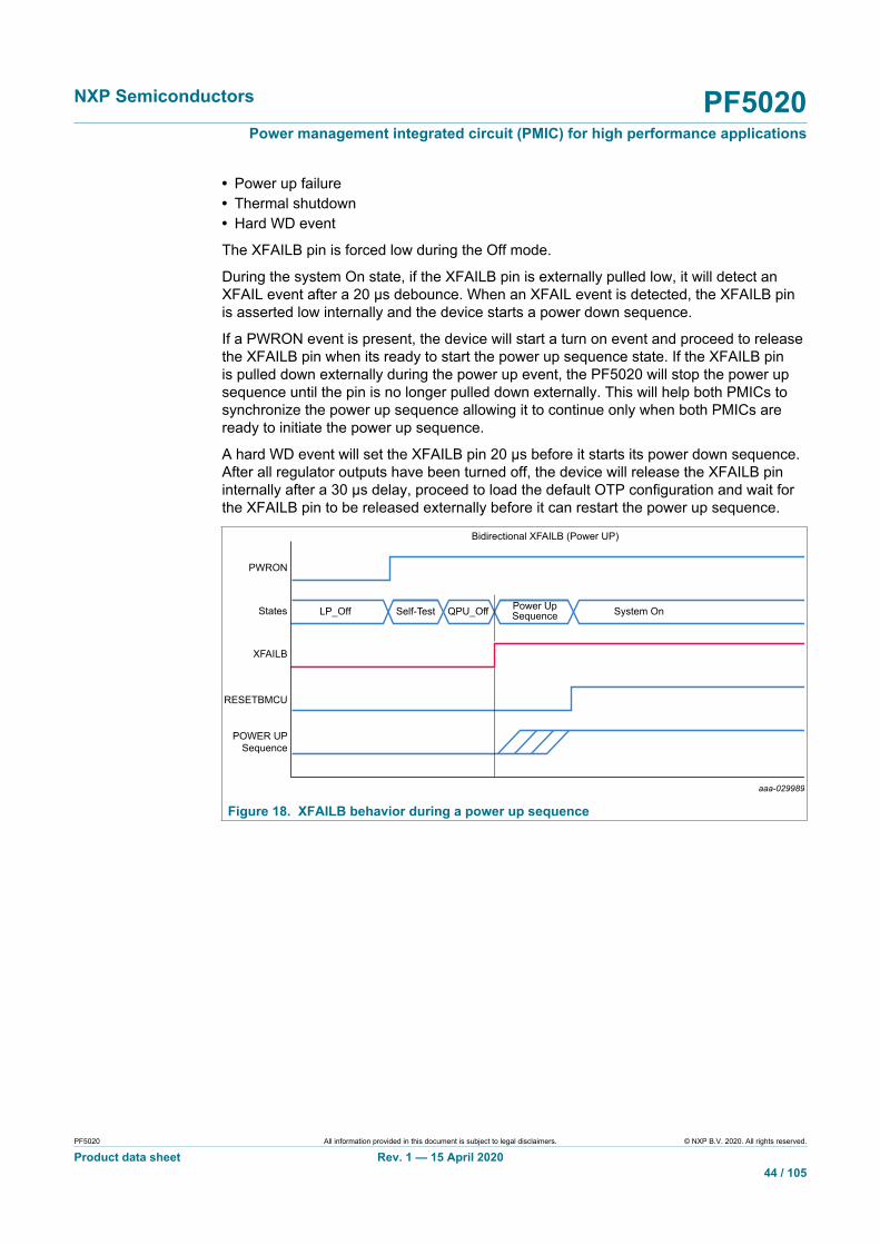
NXP Semiconductors PF5020Power management integrated circuit (PMIC) for high performance applications
PF5020 All information provided in this document is subject to legal disclaimers. © NXP B.V. 2020. All rights reserved.
Product data sheet Rev. 1 — 15 April 202044 / 105
• Power up failure• Thermal shutdown• Hard WD event
The XFAILB pin is forced low during the Off mode.
During the system On state, if the XFAILB pin is externally pulled low, it will detect anXFAIL event after a 20 µs debounce. When an XFAIL event is detected, the XFAILB pinis asserted low internally and the device starts a power down sequence.
If a PWRON event is present, the device will start a turn on event and proceed to releasethe XFAILB pin when its ready to start the power up sequence state. If the XFAILB pinis pulled down externally during the power up event, the PF5020 will stop the power upsequence until the pin is no longer pulled down externally. This will help both PMICs tosynchronize the power up sequence allowing it to continue only when both PMICs areready to initiate the power up sequence.
A hard WD event will set the XFAILB pin 20 µs before it starts its power down sequence.After all regulator outputs have been turned off, the device will release the XFAILB pininternally after a 30 µs delay, proceed to load the default OTP configuration and wait forthe XFAILB pin to be released externally before it can restart the power up sequence.
aaa-029989
Self-Test QPU_Off System OnLP_Off Power UpSequence
Bidirectional XFAILB (Power UP)
PWRON
States
XFAILB
RESETBMCU
POWER UPSequence
Figure 18. XFAILB behavior during a power up sequence

NXP Semiconductors PF5020Power management integrated circuit (PMIC) for high performance applications
PF5020 All information provided in this document is subject to legal disclaimers. © NXP B.V. 2020. All rights reserved.
Product data sheet Rev. 1 — 15 April 202045 / 105
aaa-029990
System On Off ModePower DownSequence
Bidirectional XFAILB (Power Down)
FAULT EVENT
EWARN
States
XFAILB
POWER DOWNSignal
POWER DOWNSequence
20 µs
100 µs
Figure 19. XFAILB behavior during a power down sequence
aaa-029991
Dual PMIC interaction (Fault on Master PMIC)
Power Up Sequence is starteduntil both XFAILB are pulled high
XFAILBDebounced
Pin externally pulled down
Slave Ready to start Power Up Sequence (waiting)
FAULT EVENT
MASTERPMIC
EWARN
PWRON
XFAILB
POWER DOWNSignal
POWER DOWNSequence
POWER UPSequence
20 µs
20 µs
100 µs
SLAVEPMIC
EWARN
XFAILB
POWER DOWNSignal
POWER DOWNSequence
POWER UPSequence
Figure 20. Behavior during an external XFAILB event
NXP Semiconductors PF5020Power management integrated circuit (PMIC) for high performance applications
PF5020 All information provided in this document is subject to legal disclaimers. © NXP B.V. 2020. All rights reserved.
Product data sheet Rev. 1 — 15 April 202046 / 105
aaa-029992
XFAILB During Power Up Sequence
Slave Ready to start Power Up Sequence (waiting)
Pin externally pulled down
2 msMASTERPMIC
PWRON
XFAILB
RESETBMCU
POWER DOWNSignal
POWER UPSequence
POWER UPSequence
SLAVEPMIC
XFAILB
POWER DOWNSignal
Power Up Sequence is starteduntil both XFAILB are pulled high
Figure 21. External XFAILB event during a power up sequence
14.9.11 SDA and SCL (I2C bus)
Communication with the PF5020 is done through I2C and it supports high-speedoperation mode with up to 3.4 MHz operation. SDA and SCL are pulled up to VDDIO with1.5 kΩ resistors.
The PF5020 is designed to operate as a slave device during I2C communication. Thedefault I2C device address is set by the OTP_I2C_ADD[2:0].
Table 33. I2C address configurationOTP_I2C_ADD[2:0] Device address
000 0x08
001 0x09
010 0x0A
011 0x0B
100 0x0C
101 0x0D
110 0x0E
111 0x0F
See http://www.nxp.com/documents/user_manual/UM10204.pdf for detailed informationon the digital I2C communication protocol implementation.
During an I2C transaction, the communication will latch after the 8th bit sent. If the datasent is not a multiple of 8 bit, any word with less than 8 bits will be ignored. If only 7 bitsare sent, no data is written and the logic will not provide an ACK bit to the MCU.
From an IC level, a wrong I2C command can create a system level safety issue. Forexample, though the MCU may have intended to set a given regulator’s output to 1.0 V, itmay be erroneously registered as 1.1 V due to noise in the bus.

NXP Semiconductors PF5020Power management integrated circuit (PMIC) for high performance applications
PF5020 All information provided in this document is subject to legal disclaimers. © NXP B.V. 2020. All rights reserved.
Product data sheet Rev. 1 — 15 April 202047 / 105
To prevent a wrong I2C configuration, various protective mechanisms are implemented.
14.9.11.1 I2C CRC verification
When this feature is enabled, a selectable CRC verification is performed on each I2Ctransaction.
• When OTP_I2C_CRC_EN = 0, the CRC verification mechanism is disabled.• When OTP_I2C_CRC_EN = 1, the CRC verification mechanism is enabled.
After each I2C transaction, the device calculates the corresponding CRC byte to ensurethe configuration command has not been corrupted.
When a CRC fault is detected, the PF5020 ignores the erroneous configurationcommand and triggers a CRC_I interrupt asserting the INTB pin, provided the interrupt isnot masked.
The PF5020 implements a CRC-8-SAE, per the SAE J1850 specification.
• Polynomial = 0x11D• Initial value = 0xFF
aaa-028696
7
MSB Data
6 5 4 1 03
I2C CRS PolynominalSeed: 1 1 1 1 1 1 1 1
2
Figure 22. 8 bit SAE J1850 CRC polynomial
14.9.11.2 I2C secure write
A secure write mechanism is implemented for specific registers critical to the functionalsafety of the device.
• When OTP_I2C_ SECURE_EN = 0, the secure write is disabled.• When OTP_I2C_ SECURE_EN = 1, the secure write is enabled.
When the secure write is enabled, a specific sequence must be followed in order to grantwriting access on the corresponding secure register.
Secure write sequence is as follows:
• MCU sends command to modify the secure registers• PMIC generates a random code in the RANDOM_GEN register• MCU reads the random code from the RANDOM_GEN register and writes it back on
the RANDOM_CHK register
The PMIC compares the RANDOM_CHK against the RANDOM_GEN register:
• If RANDOM_CHK [7:0] = RANDOM_GEN[7:0], the device applies the configurationon the corresponding secure register, and self-clears both the RANDOM_GEN andRANDOM_CHK registers.
• If RANDOM_CHK[7:0] different from RANDOM_GEN[7:0], the device ignores theconfiguration command and self-clears both the RANDOM_GEN and RANDOM_CHKregisters.

NXP Semiconductors PF5020Power management integrated circuit (PMIC) for high performance applications
PF5020 All information provided in this document is subject to legal disclaimers. © NXP B.V. 2020. All rights reserved.
Product data sheet Rev. 1 — 15 April 202048 / 105
In the event the MCU sends any other command instead of providing a value for theRANDOM_CHK register, the state machine cancels the ongoing secure write transactionand performs the new I2C command.
In the event the MCU does not provide a value for the RANDOM_CHK register, the I2Ctransaction will time out 10 ms after the RANDOM_GEN code is generated, and device isready for a new transaction.
Table 34. Secure bitsRegister Bit Description
ABIST OV1 AB_SW1_OV Writing a 1 to this flag to clear the ABIST faultnotification
ABIST OV1 AB_SW2_OV Writing a 1 to this flag to clear the ABIST faultnotification
ABIST OV1 AB_SWND1_OV Writing a 1 to this flag to clear the ABIST faultnotification
ABIST OV2 AB_LDO1_OV Writing a 1 to this flag to clear the ABIST faultnotification
ABIST UV1 AB_SW1_UV Writing a 1 to this flag to clear the ABIST faultnotification
ABIST UV1 AB_SW2_UV Writing a 1 to this flag to clear the ABIST faultnotification
ABIST UV1 AB_SWND1_UV Writing a 1 to this flag to clear the ABIST faultnotification
ABIST UV2 AB_LDO1_UV Writing a 1 to this flag to clear the ABIST faultnotification
ABIST RUN AB_RUN Writing a 1 starts an ABIST on demand
CTRL1 TMP_MON_EN Writing a 0 disables the thermal monitor, preventingthe thermal interrupts and thermal shutdown eventfrom being detected
CTRL1 VIN_OVLO_EN Writing a 0 disables the VIN overvoltage lockoutmonitor completely
CTRL1 WDI_MODE Writing a 0 sets the WDI event to soft WD resetWriting a 1 sets the WDI event to hard WD reset
CTRL1 VIN_OVLO_SDWN Writing a 0 disables a shutdown event upon a VINovervoltage condition (only interrupts are provided)
CTRL1 WD_EN Writing a 0 disables the watchdog counter block
CTRL1 WD_STBY_EN Writing a 0 disables the watchdog counter during thestandby mode
CTRL1 WDI_STBY_ACTIVE Writing a 0 disables the monitoring of WDI inputduring standby mode
CTRL1 I2C_SECURE_EN Writing a 0 disables de I2C secure write mode
VMONEN1 SW1VMON_EN Writing a 0 disables the OV/UV monitor for SW1
VMONEN1 SW2VMON_EN Writing a 0 disables the OV/UV monitor for SW2
VMONEN1 SWND1VMON_EN Writing a 0 disables the OV/UV monitor for SWND1
VMONEN2 LDO1VMON_EN Writing a 0 disables the OV/UV monitor for LDO1
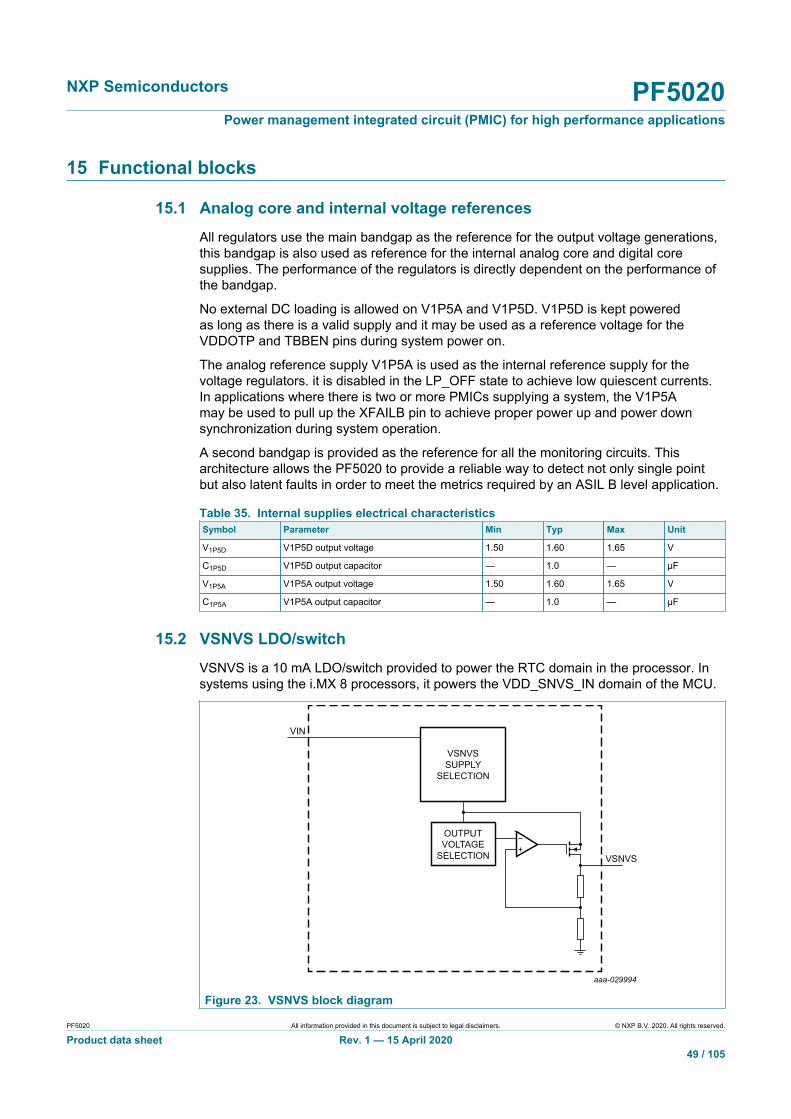
NXP Semiconductors PF5020Power management integrated circuit (PMIC) for high performance applications
PF5020 All information provided in this document is subject to legal disclaimers. © NXP B.V. 2020. All rights reserved.
Product data sheet Rev. 1 — 15 April 202049 / 105
15 Functional blocks
15.1 Analog core and internal voltage referencesAll regulators use the main bandgap as the reference for the output voltage generations,this bandgap is also used as reference for the internal analog core and digital coresupplies. The performance of the regulators is directly dependent on the performance ofthe bandgap.
No external DC loading is allowed on V1P5A and V1P5D. V1P5D is kept poweredas long as there is a valid supply and it may be used as a reference voltage for theVDDOTP and TBBEN pins during system power on.
The analog reference supply V1P5A is used as the internal reference supply for thevoltage regulators. it is disabled in the LP_OFF state to achieve low quiescent currents.In applications where there is two or more PMICs supplying a system, the V1P5Amay be used to pull up the XFAILB pin to achieve proper power up and power downsynchronization during system operation.
A second bandgap is provided as the reference for all the monitoring circuits. Thisarchitecture allows the PF5020 to provide a reliable way to detect not only single pointbut also latent faults in order to meet the metrics required by an ASIL B level application.
Table 35. Internal supplies electrical characteristicsSymbol Parameter Min Typ Max Unit
V1P5D V1P5D output voltage 1.50 1.60 1.65 V
C1P5D V1P5D output capacitor — 1.0 — µF
V1P5A V1P5A output voltage 1.50 1.60 1.65 V
C1P5A V1P5A output capacitor — 1.0 — µF
15.2 VSNVS LDO/switchVSNVS is a 10 mA LDO/switch provided to power the RTC domain in the processor. Insystems using the i.MX 8 processors, it powers the VDD_SNVS_IN domain of the MCU.
aaa-029994
OUTPUTVOLTAGE
SELECTION
VIN
VSNVS
VSNVSSUPPLY
SELECTION
Figure 23. VSNVS block diagram
NXP Semiconductors PF5020Power management integrated circuit (PMIC) for high performance applications
PF5020 All information provided in this document is subject to legal disclaimers. © NXP B.V. 2020. All rights reserved.
Product data sheet Rev. 1 — 15 April 202050 / 105
When VIN is rising and VIN > UVDET, the VSNVS is powered by VIN. When operatingfrom VIN, it can regulate the output to 1.8 V, 3.0 V or 3.3 V. If the configured outputvoltage is higher than the input source, the VSNVS operates in dropout mode to track theinput voltage.
Table 36. VSNVS output voltage configurationOTP_VSNVSVOLT[1:0] VSNVSVOLT[1:0] VSNVS output voltage (V)
00 00 OFF
01 01 1.8
10 10 3.0
11 11 3.3
The VSNVS output keeps regulation through all states, including the system On,Off modes, power down sequence, watchdog reset, fail-safe transition and fail-safestate as long as it has a valid input (VIN), and the output has been configured by theOTP_VSNVSVOLT[1:0] registers.
For system debugging purposes, the VSNVS output may be changed during the systemOn state by changing the VSNVSVOLT[1:0] bits in the functional I2C registers.
Table 37. VSNVS electrical characteristicsAll parameters are specified at TA = −40 °C to 125 °C, unless otherwise noted. Typical values are characterized at VIN =5.0 V, and TA = 25 °C, unless otherwise noted.Symbol Parameter Min Typ Max Unit
VIN_SNVS Operating voltage range from VIN 2.5 — 5.5 V
VLICELL_SNVS Operating voltage range from LICELL 1.728 — 5.5 V
ISNVS VSNVS load current range 0 — 10 mA
VSNVS_ACC VSNVS output voltage accuracy in LDO mode −5.0 — 5.0 %
VSNVS_RDSON VSNVS LDO on resistanceVSNVSVOLT[1:0] = 10 or 11
—
—
20
Ω
VSNVS_IQ VSNVS quiescent current in LDO mode — 5.0 — µA
VSNVS_HDR VSNVS LDO headroom voltageMinimum voltage above setting VSNVSVOLT[1:0] = 10or 11 to guarantee regulation with 5 % tolerance
200
—
—
mV
VSNVS_HDR VSNVS LDO headroom voltageMinimum voltage above setting VSNVSVOLT[1:0] = 01to guarantee regulation with 5 % tolerance
500
—
—
mV
VSNVS_OS VSNVS startup overshoot — — 200 mV
VSNVS_TRANS VSNVS load transient −100 — 100 mV
VSNVS_SW_R VSNVS switch mode resistanceVSNVSVOLT[1:0] = 10 or 11
—
—
20
Ω
VSNVS_LICELL_IQ VSNVS quiescent current in switch modeVSNVSVOLT[1:0] = 10 or 11
—
1.0
—
µA
VSNVS_ILIM VSNVS current limit 20 — 60 mA
VSNVS_TON VSNVS turn on timeBlock enabled to VSNVS at 90 % of final value
—
—
1.35
ms
15.3 Type 1 buck regulators (SW1 and SW2)The PF5020 features two low voltage regulators with input supply range from 2.5 Vto 5.5 V and output voltage range from 0.4 V to 1.8 V in 6.25 mV steps. Each voltage
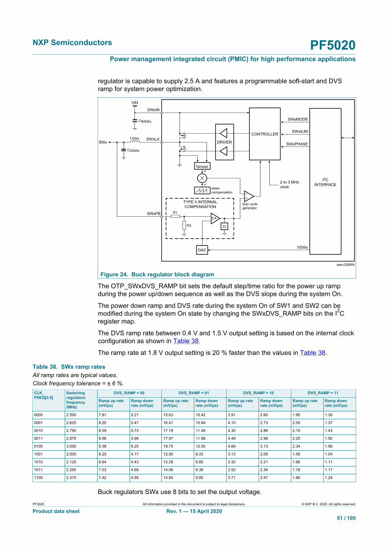
NXP Semiconductors PF5020Power management integrated circuit (PMIC) for high performance applications
PF5020 All information provided in this document is subject to legal disclaimers. © NXP B.V. 2020. All rights reserved.
Product data sheet Rev. 1 — 15 April 202051 / 105
regulator is capable to supply 2.5 A and features a programmable soft-start and DVSramp for system power optimization.
aaa-028064
I2CINTERFACE2 to 3 MHz
clock
duty cyclegenerator
slopecompensation
DAC
R2
R1
EASWxFB
TYPE II INTERNALCOMPENSATION
VSWx
SWxLX
SWxIN
SWx
VIN
CINSWx
COSWx
LSWxSWxPHASE
SWxILIM
SWxMODE
CONTROLLER
DRIVER
ISENSE
Z2
+
+
Figure 24. Buck regulator block diagram
The OTP_SWxDVS_RAMP bit sets the default step/time ratio for the power up rampduring the power up/down sequence as well as the DVS slope during the system On.
The power down ramp and DVS rate during the system On of SW1 and SW2 can bemodified during the system On state by changing the SWxDVS_RAMP bits on the I2Cregister map.
The DVS ramp rate between 0.4 V and 1.5 V output setting is based on the internal clockconfiguration as shown in Table 38.
The ramp rate at 1.8 V output setting is 20 % faster than the values in Table 38.
Table 38. SWx ramp ratesAll ramp rates are typical values.Clock frequency tolerance = ± 6 %.
DVS_RAMP = 00 DVS_RAMP = 01 DVS_RAMP = 10 DVS_RAMP = 11CLK_FREQ[3:0]
Switchingregulatorsfrequency(MHz)
Ramp up rate(mV/µs)
Ramp downrate (mV/µs)
Ramp up rate(mV/µs)
Ramp downrate (mV/µs)
Ramp up rate(mV/µs)
Ramp downrate (mV/µs)
Ramp up rate(mV/µs)
Ramp downrate (mV/µs)
0000 2.500 7.81 5.21 15.63 10.42 3.91 2.60 1.95 1.30
0001 2.625 8.20 5.47 16.41 10.94 4.10 2.73 2.05 1.37
0010 2.750 8.59 5.73 17.19 11.46 4.30 2.86 2.15 1.43
0011 2.875 8.98 5.99 17.97 11.98 4.49 2.99 2.25 1.50
0100 3.000 9.38 6.25 18.75 12.50 4.69 3.13 2.34 1.56
1001 2.000 6.25 4.17 12.50 8.33 3.13 2.08 1.56 1.04
1010 2.125 6.64 4.43 13.28 8.85 3.32 2.21 1.66 1.11
1011 2.250 7.03 4.69 14.06 9.38 3.52 2.34 1.76 1.17
1100 2.375 7.42 4.95 14.84 9.90 3.71 2.47 1.86 1.24
Buck regulators SWx use 8 bits to set the output voltage.

NXP Semiconductors PF5020Power management integrated circuit (PMIC) for high performance applications
PF5020 All information provided in this document is subject to legal disclaimers. © NXP B.V. 2020. All rights reserved.
Product data sheet Rev. 1 — 15 April 202052 / 105
• The VSWx_RUN[7:0] set the output voltage during Run mode.• The VSWx_STBY[7:0] set the output voltage during Standby mode.
The default output voltage configuration for Run and Standby modes is loaded from theOTP_VSWx[7:0] registers upon power up.
Table 39. SWx output voltage configurationSet point VSWx_RUN[7:0]
VSWx_STBY[7:0]VSWxFB (V)
0 00000000 0.40000
1 00000001 0.40625
2 00000010 0.41250
3 00000011 0.41875
.
...
.
.
175 10101111 1.49375
176 10110000 1.50000
177 10110001 1.80000
178 to 255 10110010 to 11111111 Reserved
DVS operation is available for all voltage settings between 0.4 V to 1.5 V. However,the SWx regulator is not intended to perform DVS transitions to or from the 1.8 Vconfiguration. In the event a voltage change is requested between any of the low voltagesettings and 1.8 V, the switching regulator is automatically disabled first and then re-enabled at the selected voltage level to avoid an uncontrolled transition to the newvoltage setting.
Each regulator is provided with two bits to set its mode of operation.
• The SWx_RUN_MODE[1:0] bits allow the user to change the mode of operation of theSWx regulators during the Run state. If the regulator was programmed as part of thepower up sequence, the SWx_RUN_MODE[1:0] bits are loaded with 0b11 (autoskip) bydefault. Otherwise, it is loaded with 0b00 (disabled).
• The SWx_STBY_MODE[1:0] bits allow the user to change the mode of operation ofthe SWx regulators during the Standby state. If the regulator was programmed aspart of the power up sequence, the SWx_STBY_MODE[1:0] bits are loaded with 0b11(autoskip) by default. Otherwise, it is loaded with 0b00 (disabled).
Table 40. SWx regulator mode configurationSWx_MODE[1:0] Mode of operation
00 OFF
01 PWM mode
10 PFM mode
11 Auto skip mode
The SWx_MODE_I interrupt asserts the INTB pin when any of the Type 1 regulatorshave changed the mode of operation, provided the corresponding interrupt is notmasked.
To avoid potential detection of an OV/UV fault during SWx ramp up, it is recommended topower up the regulator in PWM or autoskip mode.
NXP Semiconductors PF5020Power management integrated circuit (PMIC) for high performance applications
PF5020 All information provided in this document is subject to legal disclaimers. © NXP B.V. 2020. All rights reserved.
Product data sheet Rev. 1 — 15 April 202053 / 105
SWx regulators use 2 bits SWxILIM[1:0], to program the current limit detection.
Table 41. SWx current limit selectionSWxILIM[1:0] Typical current limit
00 2.1 A
01 2.6 A
10 3.0 A
11 4.5 A
During single phase operation, all buck regulators use 3 bits (SWxPHASE[2:0]) to controlthe phase shift of the switching frequency. Upon power up, the switching phase of allregulators is defaulted to 0 degrees and can be modified during the system On state.
Table 42. SWx phase configurationSWx_PHASE[2:0] Phase shift [degrees]
000 45
001 90
010 135
011 180
100 225
101 270
110 315
111 0 (default)
Each one of the buck regulator provides 2 OTP bits to configure the value of the inductorused in the corresponding block. The OTP_SWx_LSELECT[1:0] allows to choose theinductor as shown in Table 43.
Table 43. SWx inductor selection bitsOTP_SWx_LSELECT[1:0] Inductor value
00 1.0 µH
01 0.47 µH
10 1.5 µH
11 Reserved
15.3.1 SW2 VTT operation
SW2 features a selectable VTT mode to create VTT termination for DDR memories.
When SW2_VTTEN = 1, the VTT mode is enabled. In this mode, SW2 reference voltageis internally connected to SW1FB output through a divider by 2.
During the VTT mode, the DVS operation on SW2 is disabled and SW2 output is givenby VSW1FB / 2. In this mode, the minimum output voltage configuration for SW1 should be800 mV to ensure the SW2 is still within the regulation range at its output.
During the power up sequence, the SW2 (VTT) may be turned on in the same or at a slothigher than SW1, as required by the system. When SW2 and SW1 are enabled in thesame slot, SW2 will always track the VSW1/2. When SW2 is enabled after SW1, it willramp up gradually to a predefined voltage and once this voltage is reached, it will start
NXP Semiconductors PF5020Power management integrated circuit (PMIC) for high performance applications
PF5020 All information provided in this document is subject to legal disclaimers. © NXP B.V. 2020. All rights reserved.
Product data sheet Rev. 1 — 15 April 202054 / 105
tracking VSW1/2. The user may adjust the value at which the SW2 should start trackingthe voltage on the SW1 regulator by setting the OTP_VSW2 register accordingly.
During normal operation, if the SW1 is disabled via the I2C command, SW2 tracks theoutput of SW1 and both regulators are discharged together and pulled down internally.When SW1 is enabled back via the I2C commands, the SW1 output ramps up to thecorresponding voltage while SW2 is always VSW1/2.
When only SW2 is disabled the PMIC uses the OTP_VTT_PDOWN bit to programwhether the SW2 regulator is disabled with the output in high impedance or dischargedinternally.
• When OTP_VTT_PDOWN = 0, the output is disabled in high impedance mode.• When OTP_VTT_PDOWN = 1, the output is disabled with the internal pull down
enabled.
When SW2 is requested to enable back again, the SW2 ramps up to the voltage set onthe VSW2_RUN or VSW2_STBY registers. Once it reaches the final DVS value, it willchange its reference to start tracking SW1 output again. Note that VSW2_RUN(STBY)must be set to VSW1_RUN(STBY)/2 or the closest code by the MCU to ensure properoperation.
When operating in VTT mode, the minimum output voltage configuration for SW1 shouldbe 800 mV to ensure the SW2 is still within the regulation range at its output.
15.3.2 Multiphase operation
Regulators SW1 and SW2 can be configured in dual phase mode. In this mode, SW1registers control the output voltage and other configurations. Likewise, SW1FB pinbecomes the main feedback node for the resulting voltage rail, however the two FB pinsshould be connected together.
The OTP_SW1CONFIG[1:0] bits are used to select the multiphase configuration forSW1/SW2.
Table 44. OTP_SW1CONFIG register descriptionOTP_SW1CONFIG[1:0] Description
00 SW1 and SW2 operate in single phase mode
01 SW1/SW2 operate in dual phase mode
10 Reserved
11 Reserved
15.3.3 Electrical characteristics
Table 45. Type 1 buck regulator electrical characteristicsAll parameters are specified at TA = −40 to 125 °C, VSWxIN = UVDET to 5.5 V, VSWxFB = 1.0 V, ISWx = 500 mA, typicalexternal component values, fSW = 2.25 MHz, unless otherwise noted. Typical values are characterized at VSWxIN = 5.0 V,VSWxFB = 1.0 V, ISWx = 500 mA, and TA = 25 °C, unless otherwise noted.Symbol Parameter [1][2] Min Typ Max Unit
VSWxIN Operating functional input voltage UVDET — 5.5 V
VSWxACC Output voltage accuracyPWM mode0.4 V ≤ VSWxFB ≤ 0.8 V0 ≤ ISWx ≤ 2.5 A
−10
—
10
mV

NXP Semiconductors PF5020Power management integrated circuit (PMIC) for high performance applications
PF5020 All information provided in this document is subject to legal disclaimers. © NXP B.V. 2020. All rights reserved.
Product data sheet Rev. 1 — 15 April 202055 / 105
Symbol Parameter [1][2] Min Typ Max Unit
VSWxACC Output voltage accuracyPWM mode0.8 V < VSWxFB ≤ 1.5 V0 ≤ ISWx ≤ 2.5 A
−2.0
—
2.0
%
VSWxACC Output voltage accuracyPWM modeVSWxFM = 1.1 V0 ≤ ISWx ≤ 2.5 A
−1.5
—
1.5
%
VSWxACC Output voltage accuracyPWM modeVSWxFB = 1.8 V0 ≤ ISWx ≤ 2.5 A
−2.0
—
2.0
%
VSWxACCPFM Output voltage accuracyPFM mode0.4 V ≤ VSWxFB ≤ 1.5 V0 ≤ ISWx ≤ 100 mA
−36
—
36
mV
VSWxACCPFM Output voltage accuracyPFM modeVSWxFB = 1.8 V0 ≤ ISWx ≤ 100 mA
−57
—
57
mV
tPFMtoPWM PFM to PWM transition time 30 — — µs
ISWx Max load current in single phase 2500 — — mA
ISWx_DP Max load current in dual phase 5000 — — mA
ISWxLIM Current limiter - inductor peak current detectionSWxILIM[1:0] = 00
1.6
2.1
2.5
A
ISWxLIM Current limiter - inductor peak current detectionSWxILIM[1:0] = 01
2.0
2.6
3.1
A
ISWxLIM Current limiter - inductor peak current detectionSWxILIM[1:0] = 10
2.4
3.0
3.7
A
ISWxLIM Current limiter - inductor peak current detectionSWxILIM[1:0] = 11
3.6
4.5
5.45
A
ISWxNLIM Negative current limit in single phase mode 0.6 1.0 1.4 A
ISWxxLIM_DP Current limit in dual phase operationSWxILIM = 00 (master)
3.2
4.2
5.0
A
ISWxxLIM_DP Current limit in dual phase operationSWxILIM = 01 (master)
4.0
5.2
6.2
A
ISWxxLIM_DP Current limit in dual phase operationSWxILIM = 10 (master)
4.8
6.0
7.4
A
ISWxxLIM_DP Current limit in dual phase operationSWxILIM = 11 (master)
7.2
9.0
10.9
A
VSWxOSH Startup overshootSWxDVS RAMP = 6.25 mV/µsVSWxIN = 5.5 V, VSWxFB= 1.0 V
−25
25
50
mV
tONSWxMAX Maximum turn on timeFrom enable to 90 % of end valueSWxDVS RAMP = 11 (1.56 mV/µs, 2 MHz)VSWxIN = 5.5 V, VSWxFB= 1.5 V
—
—
895
µs
tONSWx_MIN Minimum turn on timeFrom enable to 90 % of end valueSWxDVS RAMP = 01 (18.75 mV/µs, 3 MHz)VSWxIN = 5.5 V, VSWxFB= 0.4 V
49.2
—
—
µs
ηSWx Efficiency (PFM mode, 1.0 V, 1.0 mA) — 80 — %
ηSWx Efficiency (PFM mode, 1.0 V, 50 mA) — 81 — %
ηSWx Efficiency ( PFM Mode, 1.0 V, 100 mA) — 82 — %
NXP Semiconductors PF5020Power management integrated circuit (PMIC) for high performance applications
PF5020 All information provided in this document is subject to legal disclaimers. © NXP B.V. 2020. All rights reserved.
Product data sheet Rev. 1 — 15 April 202056 / 105
Symbol Parameter [1][2] Min Typ Max Unit
ηSWx Efficiency (PWM mode, 1.0 V, 500 mA) — 83 — %
ηSWx Efficiency (PWM mode, 1.0 V, 1000 mA) — 82 — %
ηSWx Efficiency (PWM mode, 1.0 V, 2000 mA) — 79 — %
VSWxLOTR Transient load regulation (overshoot/undershoot)at 0.8 V < VSWxFB ≤ 1.2 V, COUT = 44 µF per phase
ILOAD = 200 mA to 1.0 A, di/dt = 2.0 A/µs (Singlephase)ILOAD = 400 mA to 2.0 A, di/dt = 4.0 A/µs (Dualphase)
−25
—
25
mV
VSWxLOTR Transient load regulation (overshoot/undershoot)at 1.25 V < VSWxFB ≤ 1.8 V, COUT = 44 µF per phase
ILOAD = 200 mA to 1.0 A, di/dt = 2.0 A/µs (Singlephase)ILOAD = 400 mA to 2.0 A, di/dt = 4.0 A/µs (Dualphase)
−3.0
—
3.0
%
FSWx PWM switching frequency rangeFrequency set by CLK_FREQ[3:0]
1.9
2.5
3.15
MHz
TOFFminSWx Minimum off time — 27 — ns
TDBSWx Deadband time — 3.0 — ns
Tslew Slewing time (10 % to 90 %) — — 5.0 ns
DVSWx Output ripple in PWM modeat VSWxFB = 1.0 V
—
—
1.0
%
IRCS DCM (skip mode) reverse current sense thresholdCurrent flowing from PGND to SWxLX
−200
—
200
mA
ISWxQ Quiescent currentPFM mode
—
14
—
µA
ISWxQ Quiescent currentAuto skip mode
—
160
250
µA
ISWxQ_DP Quiescent current in dual phase PWM mode — 200 320 µA
RONSWxHS SWx high-side P-MOSFET RDS(on)[3] — — 135 mΩ
RONSWxLS SWx low-side N-MOSFET RDS(on)[3] — — 80 mΩ
RSWxDIS Discharge resistanceRegulator disabled and ramp down completed
50
100
200
Ω
[1] For VSWx configurations greater than 1.35 V, full parametric operation is guaranteed for 2.7 V < SWxVIN < 5.5 V. Below 2.7 V, the SWx regulators arefully functional with degraded operation due to headroom limitation.
[2] For VSWx = 1.8 V, output capacitance should be kept at or below the maximum recommended value. Likewise, it is recommended to use the slow turnon/off ramp rate to ensure the output is discharged completely when it is disabled.
[3] Max RDS(on) does not include bondwire resistance. Consider +/- 50 % tolerance to account for bondwire and pin loss.
Table 46. Recommended external componentsSymbol Parameter Min Typ Max Unit
L Output inductorMaximum inductor DC resistance 50 mΩMinimum saturation current at full load: 3.0 A
[1] 0.47
1.0
1.5
µH
Cout Output capacitorUse 2 × 22 µF, 6.3 V X7T ceramic capacitor toreduce output capacitance ESR
35
44
53
µF
Cin Input capacitor4.7 μF, 10 V X7R ceramic capacitor
4.23
4.7
5.17
µF
[1] Keep inductor DCR as low as possible to improve regulator efficiency.
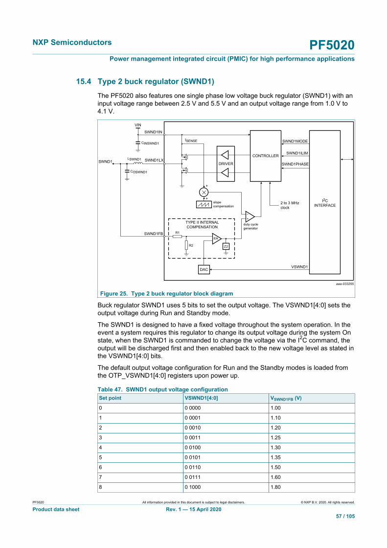
NXP Semiconductors PF5020Power management integrated circuit (PMIC) for high performance applications
PF5020 All information provided in this document is subject to legal disclaimers. © NXP B.V. 2020. All rights reserved.
Product data sheet Rev. 1 — 15 April 202057 / 105
15.4 Type 2 buck regulator (SWND1)The PF5020 also features one single phase low voltage buck regulator (SWND1) with aninput voltage range between 2.5 V and 5.5 V and an output voltage range from 1.0 V to4.1 V.
aaa-033255
I2CINTERFACE2 to 3 MHz
clock
duty cyclegenerator
slopecompensation
ISENSE
DAC
R2
R1
EASWND1FB
TYPE II INTERNALCOMPENSATION
VSWND1
SWND1LX
SWND1IN
SWND1
VIN
CINSWND1
COSWND1
LSWND1SWND1PHASE
SWND1ILIM
SWND1MODE
CONTROLLER
DRIVER
Z2
+
+
Figure 25. Type 2 buck regulator block diagram
Buck regulator SWND1 uses 5 bits to set the output voltage. The VSWND1[4:0] sets theoutput voltage during Run and Standby mode.
The SWND1 is designed to have a fixed voltage throughout the system operation. In theevent a system requires this regulator to change its output voltage during the system Onstate, when the SWND1 is commanded to change the voltage via the I2C command, theoutput will be discharged first and then enabled back to the new voltage level as stated inthe VSWND1[4:0] bits.
The default output voltage configuration for Run and the Standby modes is loaded fromthe OTP_VSWND1[4:0] registers upon power up.
Table 47. SWND1 output voltage configurationSet point VSWND1[4:0] VSWND1FB (V)
0 0 0000 1.00
1 0 0001 1.10
2 0 0010 1.20
3 0 0011 1.25
4 0 0100 1.30
5 0 0101 1.35
6 0 0110 1.50
7 0 0111 1.60
8 0 1000 1.80

NXP Semiconductors PF5020Power management integrated circuit (PMIC) for high performance applications
PF5020 All information provided in this document is subject to legal disclaimers. © NXP B.V. 2020. All rights reserved.
Product data sheet Rev. 1 — 15 April 202058 / 105
Set point VSWND1[4:0] VSWND1FB (V)
9 0 1001 1.85
10 0 1010 2.00
11 0 1011 2.10
12 0 1100 2.15
13 0 1101 2.25
14 0 1110 2.30
15 0 1111 2.40
16 1 0000 2.50
17 1 0001 2.80
18 1 0010 3.15
19 1 0011 3.20
20 1 0100 3.25
21 1 0101 3.30
22 1 0110 3.35
23 1 0111 3.40
24 1 1000 3.50
25 1 1001 3.80
26 1 1010 4.00
27 1 1011 4.10
28 1 1100 4.10
29 1 1101 4.10
30 1 1110 4.10
31 1 1111 4.10
Regulator SWND1 is provided with 2 bits to set its mode of operation.
• The SWND1_RUN_MODE[1:0] bits allow the user to change the mode of operation ofthe SWND1 regulators during the run state. If the regulator was programmed as partof the power up sequence, the SWND1_RUN_MODE[1:0] bits are loaded with 0b11(autoskip) by default. Otherwise, it is loaded with 0b00 (disabled).
• The SWND1_STBY_MODE[1:0] bits allow the user to change the mode of operationof the SWND1 regulators during the standby state. If the regulator was programmedas part of the power up sequence, the SWND1_STBY_MODE[1:0] bits are loaded with0b11 (autoskip) by default. Otherwise, it is loaded with 0b00 (disabled).
Table 48. SWND1 regulator mode configurationSWND1_MODE[1:0] Mode of operation
00 OFF
01 PWM mode
10 PFM mode
11 Autoskip mode
The SWND1_MODE_I interrupt asserts the INTB pin when the SWND1 regulator haschanged the mode of operation, provided the corresponding interrupt is not masked.

NXP Semiconductors PF5020Power management integrated circuit (PMIC) for high performance applications
PF5020 All information provided in this document is subject to legal disclaimers. © NXP B.V. 2020. All rights reserved.
Product data sheet Rev. 1 — 15 April 202059 / 105
When the device toggles from Run to Standby mode, the SWND1 output voltageremains the same, unless the regulator is enabled/disabled by the correspondingSWND1_RUN_MODE[1:0] or SWND1_STBY_MODE[1:0] bits.
The SWND1ILIM [1:0] bits are used to program the current limit detection level ofSWND1.
Table 49. SWND1 current limit selectionSWND1ILIM[1:0] Typical current limit
00 2.1 A
01 2.6 A
10 3.0 A
11 4.5 A
Regulator SWND1 uses 3 bits (SWxPHASE[2:0]) to control the phase shift of theswitching frequency. Upon power up, the switching phase is defaulted to 0° and can bemodified during the system On state.
Table 50. SWND1 phase configurationSWND1_PHASE[2:0] Phase shift (°)
000 45
001 90
010 135
011 180
100 225
101 270
110 315
111 0
SWND1 buck regulator provide 2 OTP bits to configure the value of the inductor usedin the power stage. The OTP_SWND1_LSELECT[1:0] allow to choose the inductor asshown in Table 51.
Table 51. SWND1 inductor selection bitsOTP_SWND1_LSELECT[1:0] Inductor value
00 1.0 µH
01 0.47 µH
10 1.5 µH
11 Reserved
15.4.1 Electrical characteristics
Table 52. Type 2 buck regulator electrical characteristicsAll parameters are specified at TA = −40 to 125 °C, VIN = VSWND1IN = UVDET to 5.5 V, VSWND1FB = 1.8 V, ISWND1 = 500 mA,typical external component values, fSW = 2.25 MHz, unless otherwise noted. Typical values are characterized at VSWND1IN =5.0 V, VSWND1FB = 1.8 V, ISWND1 = 500 mA, and TA = 25 °C, unless otherwise noted.Symbol Parameter Min Typ Max Unit
VSWND1IN Operating input voltage range1.2 V < VSWND1FB ≤ 1.85 V, DCR ≤ 40 mΩ
UVDET
—
5.5
V

NXP Semiconductors PF5020Power management integrated circuit (PMIC) for high performance applications
PF5020 All information provided in this document is subject to legal disclaimers. © NXP B.V. 2020. All rights reserved.
Product data sheet Rev. 1 — 15 April 202060 / 105
Symbol Parameter Min Typ Max Unit
VSWND1IN Operating input voltage range1.85 V < VSWND1FB < 4.5 V, DCR ≤ 40 mΩ
VSWND1FB +0.65
—
5.5
V
VSWND1ACC Output voltage accuracyPWM mode0 ≤ ISWND1 ≤ 2.5 A
−2.0
—
2.0
%
VSWND1ACC Output voltage accuracyPFM mode0 ≤ ISWND1 ≤ ΔI/2
−4.0
—
4.0
%
tPFMtoPWM PFM to PWM transition time 10 — — µs
ISWND1 Maximum output load 2500 — — mA
ISWND1LIM Current limiter - inductor peak current detectionSWND1ILIM = 00
1.6
2.1
2.5
A
ISWND1LIM Current limiter - inductor peak current detectionSWND1ILIM = 01
2.0
2.6
3.1
A
ISWND1LIM Current limiter - inductor peak current detectionSWND1ILIM = 10
2.4
3.0
3.7
A
ISWND1LIM Current limiter - inductor peak current detectionSWND1ILIM = 11
3.6
4.5
5.45
A
ISWND1NILIM Negative current limit - inductor valley current detection 0.7 1.0 1.3 A
tSWND1RAMP Soft-start ramp time during power up and power downVSWND1FB = 1.8 V
90
—
200
µs
tONSWND1 Turn on timeFrom regulator enabled to 90 % of end valueVSWND1FB = 1.8 V
100
180
300
µs
VSWND1OSH Startup overshoot −50 — 50 mV
ηSWND1 EfficiencyPFM mode, 3.3 V, 1.0 mA, TJ = 125 °C
—
85
—
%
ηSWND1 EfficiencyPFM mode, 3.3 V, 50 mA, TJ = 125 °C
—
88
—
%
ηSWND1 EfficiencyPFM mode, 3.3 V, 100 mA, TJ = 125 °C
—
90
—
%
ηSWND1 EfficiencyPWM mode, 3.3 V, 400 mA, TJ = 125 °C
—
91
—
%
ηSWND1 EfficiencyPWM mode, 3.3 V, 1000 mA, TJ = 125 °C
—
92
—
%
ηSWND1 EfficiencyPWM mode, 3.3 V, 2000 mA, TJ = 125 °C
—
90
—
%
FSWx PWM switching frequency rangeFrequency set by CLK_FREQ[3:0]
1.9
2.5
3.15
MHz
TONminSWND1 Minimum on time — 50 — ns
TDBSWND1 Deadband time — 3.0 — ns
Tslew Slewing time10 % to 90 %VSWND1IN = 5.5 V
—
—
5.0
ns
ΔVSWND1 Output rippleOutput cap ESR ~ 10 mΩ, 2 × 22 µF
−1.0
—
1.0
%
VSWND1LOTR Transient load regulation (overshoot/undershoot)at VSWND1FB = 1.8 V, COUT = 44 µFILOAD = 200 mA to 1.0 A, di/dt = 2.0 A/µs
−50
—
50
mV
IRCS DCM (skip mode) reverse current sense threshold — 10 — mA
ISWND1Q Quiescent currentPFM mode
—
18
—
µA
NXP Semiconductors PF5020Power management integrated circuit (PMIC) for high performance applications
PF5020 All information provided in this document is subject to legal disclaimers. © NXP B.V. 2020. All rights reserved.
Product data sheet Rev. 1 — 15 April 202061 / 105
Symbol Parameter Min Typ Max Unit
ISWND1Q Quiescent currentAuto skip mode
—
150
250
µA
RONSWND1HS SWND1 high-side P-MOSFET RDS(on)[1] — — 135 mΩ
RONSWND1LS SWND1 low-side N-MOSFET RDS(on)[1] — — 80 mΩ
RSWND1DIS SWND1 discharge resistance (normal operation) — 100 200 Ω
RSWND1TBB SWND1 discharge resistance during TBB modeTBBEN = 1 and QPU_OFF state
1.0
2.0
3.0
kΩ
[1] Max RDS(on) does not include bondwire resistance. Consider +/- 50 % tolerance to account for bondwire and pin loss.
Table 53. Recommended external componentsSymbol Parameter Min Typ Max Unit
L Output inductorMaximum inductor DC resistance 50 mΩMinimum saturation current at full load: 3.0 A
[1] 0.47
1.0
1.5
µH
Cout Output capacitorUse 2 × 22 μF, 6.3 V X7T ceramic capacitor toreduce output capacitance ESR
—
44
—
µF
Cin Input capacitor4.7 μF, 10 V X7R ceramic capacitor
—
4.7
—
µF
[1] Keep inductor DCR as low as possible to improve regulator efficiency.
15.5 Linear regulatorThe PF5020 has one low-dropout (LDO) regulator with the following features:
• 400 mA current capability• Input voltage range from 2.5 V to 5.5 V• Programmable output voltage between 1.5 V and 5.0 V• Soft-start ramp control during power up (enable)• Discharge mechanism during power down (disable)• OTP programmable load switch mode
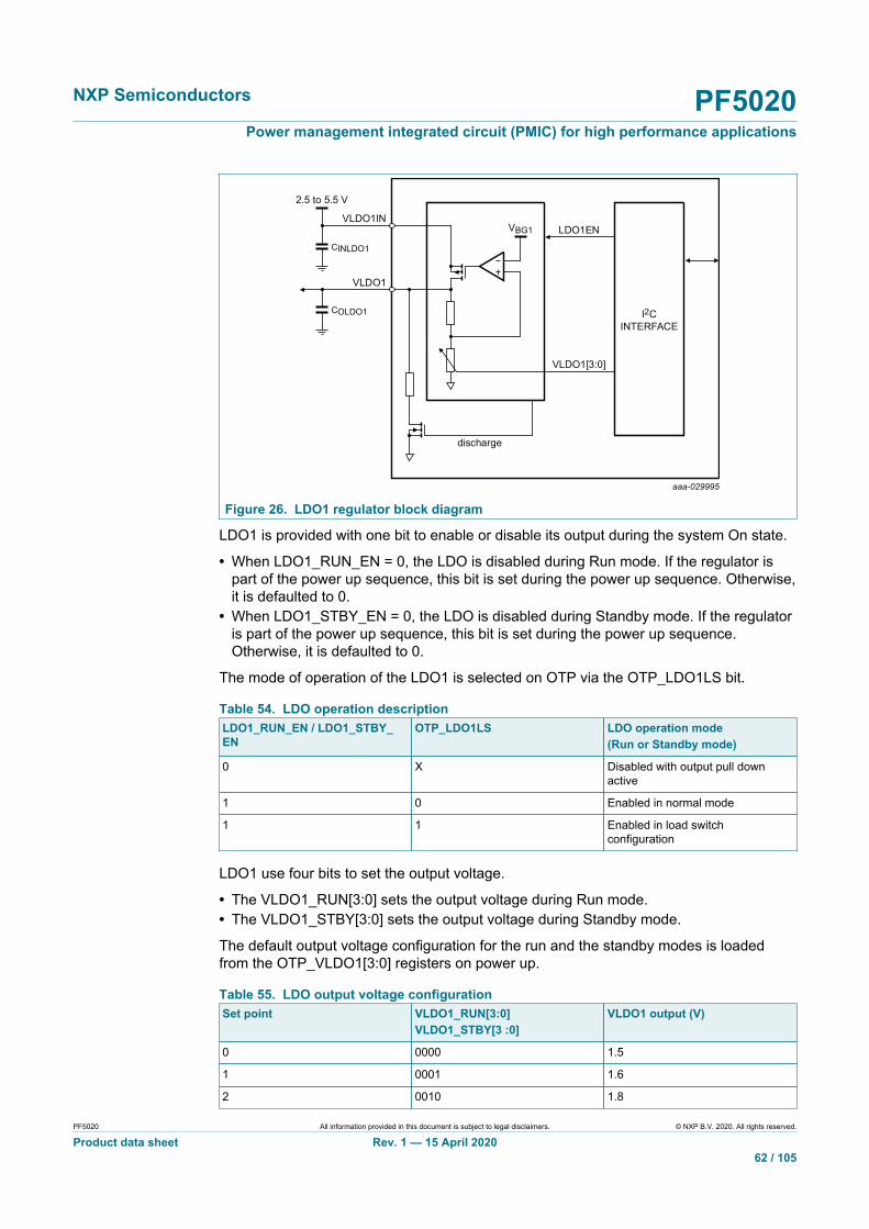
NXP Semiconductors PF5020Power management integrated circuit (PMIC) for high performance applications
PF5020 All information provided in this document is subject to legal disclaimers. © NXP B.V. 2020. All rights reserved.
Product data sheet Rev. 1 — 15 April 202062 / 105
aaa-029995
I2CINTERFACE
discharge
VLDO1
VLDO1INVBG1
2.5 to 5.5 V
CINLDO1
COLDO1
LDO1EN
VLDO1[3:0]
Figure 26. LDO1 regulator block diagram
LDO1 is provided with one bit to enable or disable its output during the system On state.
• When LDO1_RUN_EN = 0, the LDO is disabled during Run mode. If the regulator ispart of the power up sequence, this bit is set during the power up sequence. Otherwise,it is defaulted to 0.
• When LDO1_STBY_EN = 0, the LDO is disabled during Standby mode. If the regulatoris part of the power up sequence, this bit is set during the power up sequence.Otherwise, it is defaulted to 0.
The mode of operation of the LDO1 is selected on OTP via the OTP_LDO1LS bit.
Table 54. LDO operation descriptionLDO1_RUN_EN / LDO1_STBY_EN
OTP_LDO1LS LDO operation mode(Run or Standby mode)
0 X Disabled with output pull downactive
1 0 Enabled in normal mode
1 1 Enabled in load switchconfiguration
LDO1 use four bits to set the output voltage.
• The VLDO1_RUN[3:0] sets the output voltage during Run mode.• The VLDO1_STBY[3:0] sets the output voltage during Standby mode.
The default output voltage configuration for the run and the standby modes is loadedfrom the OTP_VLDO1[3:0] registers on power up.
Table 55. LDO output voltage configurationSet point VLDO1_RUN[3:0]
VLDO1_STBY[3 :0]VLDO1 output (V)
0 0000 1.5
1 0001 1.6
2 0010 1.8

NXP Semiconductors PF5020Power management integrated circuit (PMIC) for high performance applications
PF5020 All information provided in this document is subject to legal disclaimers. © NXP B.V. 2020. All rights reserved.
Product data sheet Rev. 1 — 15 April 202063 / 105
Set point VLDO1_RUN[3:0]VLDO1_STBY[3 :0]
VLDO1 output (V)
3 0011 1.85
4 0100 2.15
5 0101 2.5
6 0110 2.8
7 0111 3.0
8 1000 3.1
9 1001 3.15
10 1010 3.2
11 1011 3.3
12 1100 3.35
13 1101 4.0
14 1110 4.9
15 1111 5.0
15.5.1 LDO load switch operation
When the LDO1LS bit is set to 1, the corresponding LDO operates as a load switch,allowing a pass-through from the LDO1VIN to the LDO1VOUT output through a typical130 mΩ resistance. In this mode of operation, the input must be kept inside the LDOoperating input voltage range (2.5 V to 5.5 V)
The LDO1EN bit is used to enable or disable the switch.
15.5.2 LDO regulator electrical characteristics
Table 56. LDO regulator electrical characteristicsAll parameters are specified at TA = −40 to 125 °C, VLDO1IN = 2.5 V to 5.5 V, VLDO1 = 1.8 V, ILDO1 = 100 mA, typical externalcomponent values, unless otherwise noted. Typical values are characterized at VLDO1IN = 5.5 V, VLDO1 = 1.8 V, ILDO1 = 100mA, and TA = 25 °C, unless otherwise noted.Symbol Parameter Min Typ Max Units
VLDO1IN LDO1 operating input voltage range1.5 V ≤ VLDO1 < 2.25 V
2.5
—
5.5
V
VLDO1IN LDO1 operating input voltage range2.25 V < VLDO1 < 5.0 V
VLDO1NOM + 0.25
—
5.5
V
ILDO1 Maximum load current 400 — — mA
VLDO1TOL Output voltage tolerance1.5 V ≤ VLDO1 ≤ 5.0 V0 mA < ILDO1 ≤ 400 mA
−3.0
—
3.0
%
VLDO1LOR Load regulation — 0.10 0.20 mV/mA
VLDO1LIR Line regulation — 1.0 20 mV/V
ILDO1LIM Current limitILDO1 when VLDO1 is forced to VLDO1NOM/2
450
800
1200
mA
ILDO1Q Quiescent current (measured at TA = 25 °C) — 9.4 12.5 μA
RDS(on) Drop-out/load switch on resistanceVLDOINx = 3.3 V (at TJ =125 °C)
[1] —
—
130
mΩ
NXP Semiconductors PF5020Power management integrated circuit (PMIC) for high performance applications
PF5020 All information provided in this document is subject to legal disclaimers. © NXP B.V. 2020. All rights reserved.
Product data sheet Rev. 1 — 15 April 202064 / 105
Symbol Parameter Min Typ Max Units
PSRRVLDO1 DC PSRRILDO1 = 150 mAVLDO1[3:0] = 0000 to 1111VLDOINx = VLDO1INMIN
48
—
—
dB
TRVLDO1 Turn on rise time (soft-start ramp)10 % to 90 % of end valueVLDO1 = 3.3 VILDO1 = 0.0 mA
—
220
360
μs
tONLDO1 Turn on timeEnable to 90 % of end valueVLDO1 = 5.0 VILDO1 = 0.0 mA
—
—
500
μs
tOFFLDO1 Turn off timeDisable to 10 % of initial valueVLDO1 = 5.0 VILDO1 = 0.0 mA
—
—
2500
μs
VLDO1OSHT Startup overshootVLDOINx = VLDOINxMINVLDO1 = 5.0 VILDO1 = 0.0 mA
—
1.0
2.0
%
VLDO1LOTR Transient load responseILDO1 = 10 mA to 200 mA in 2.0 μsPeak of overshoot or undershoot of LDO1 withrespect to final value
−3.0
—
3.0
%
TonLDO1LS Load switch mode turn on rise time — 100 500 µs
RdischLDO1 Output discharge resistance when LDO is disabledLDO and switch mode
45
90
135
Ω
ILSxLIM Load switch mode current limit when enabledLSxILIM_EN = 1
450
800
1200
mA
RLDO1TBB LDO1 pull-down resistance during TBB modeTBBEN = 1 and in QPU_OFF state
1.0
2
—
kΩ
[1] Maximum RDS(on) resistance does not include bondwire resistance. Consider ± 50 % tolerance to account for bondwire and pin losses.
15.6 Voltage monitoringThe PF5020 provides OV and UV monitoring capability for the following voltageregulators:
• SW1, SW2 and SWND1• LDO1
A programmable UV threshold is selected via the OTP_SWxUV_TH[1:0] andOTP_LDOxUV_TH[1:0] bits. UV threshold selection represents a percentage of thenominal voltage programmed on each regulator.
Table 57. UV threshold configuration registerOTP_SWxUV_TH[1:0]OTP_LDOxUV_TH[1:0]
UV threshold level
00 95 %
01 93 %
10 91 %
11 89 %
NXP Semiconductors PF5020Power management integrated circuit (PMIC) for high performance applications
PF5020 All information provided in this document is subject to legal disclaimers. © NXP B.V. 2020. All rights reserved.
Product data sheet Rev. 1 — 15 April 202065 / 105
A programmable OV threshold is selected via the OTP_SWxOV_TH[1:0] andOTP_LDOxOV_TH[1:0] bits. OV threshold selection represents a percentage of thenominal voltage programmed on each regulator.
Table 58. OV threshold configuration registerOTP_SWxOV_THOTP_LDOxOV_TH
OV threshold level
00 105 %
01 107 %
10 109 %
11 111 %
Two functional bits are provided to program the UV debounce time for the voltageregulators.
Table 59. UV debounce timer configurationUV_DB[1:0] UV debounce time
00 5 µs
01 15 µs
10 30 µs
11 40 µs
The default value of the UV_DB[1:0] upon a full register reset is 0b10.
Two functional bits to program the OV debounce time for all the voltage regulators.
Table 60. OV debounce timer configurationOV_DB[1:0] OV debounce time
00 30 µs
01 50 µs
10 80 µs
11 125 µs
The default value of the OV_DB[1:0] upon a full register reset is 0b00.
The VMON_EN bits enable or disable the OV/UV monitor for each one of the externalregulators (SWxVMON_EN, LDOxVMON_EN).
• When the VMON_EN bit of a specific regulator is 1, the voltage monitor for that specificregulator is enabled.
• When the VMON_EN bit of a specific regulator is 0, the voltage monitor for that specificregulator is disabled.
By default, the VMON_EN bits are set to 1 on power up.
When the I2C_SECURE_EN = 1, a secure write must be performed to set or clear theVMON_EN bits to enable or disable the voltage monitoring for a specific regulator.
On enabling a regulator, the UV/OV monitor is masked until the corresponding regulatorreaches the point of regulation. If a voltage monitor is disabled, the UV_S and OV_Sindicators from that monitor are reset to 0.
Figure 27 shows the PF5020 voltage monitoring architecture.
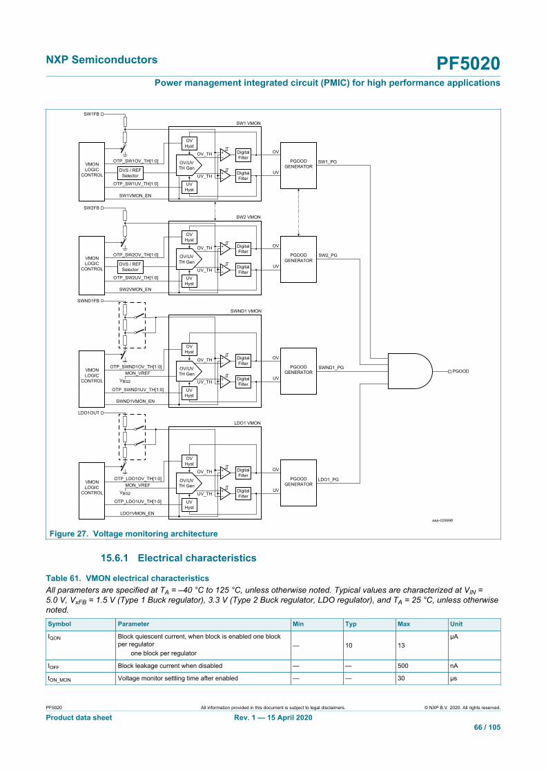
NXP Semiconductors PF5020Power management integrated circuit (PMIC) for high performance applications
PF5020 All information provided in this document is subject to legal disclaimers. © NXP B.V. 2020. All rights reserved.
Product data sheet Rev. 1 — 15 April 202066 / 105
aaa-029996
OV/UVTH Gen
OVHyst
OV
SW1_PG
SW1 VMON
UV
DigitalFilter
PGOODGENERATOR
UVHyst
OTP_SW1OV_TH[1:0]VMONLOGIC
CONTROL
SW1FB
OTP_SW1UV_TH[1:0]
SW1VMON_EN
DigitalFilter
OV/UVTH Gen
OVHyst
OV
SW2 VMON
UV
DigitalFilter
PGOODGENERATOR
UVHyst
OTP_SW2OV_TH[1:0]VMONLOGIC
CONTROL
SW2FB
OTP_SW2UV_TH[1:0]
SW2VMON_EN
SWND1VMON_EN
DigitalFilter
OV_TH
UV_TH
OV_TH
UV_TH
OV/UVTH Gen
OVHyst
OV
UV
DigitalFilter
PGOODGENERATOR
UVHyst
OTP_SWND1OV_TH[1:0]
SWND1 VMON
SWND1_PG
SW2_PG
MON_VREFVBG2
VMONLOGIC
CONTROL
SWND1FB
PGOOD
OTP_SWND1UV_TH[1:0]
DigitalFilter
OV_TH
UV_TH
OV/UVTH Gen
OVHyst
OV
LDO1_PG
LDO1 VMON
UV
DigitalFilter
PGOODGENERATOR
UVHyst
OTP_LDO1OV_TH[1:0]MON_VREF
VBG2
VMONLOGIC
CONTROL
LDO1OUT
OTP_LDO1UV_TH[1:0]
LDO1VMON_EN
DigitalFilter
OV_TH
UV_TH
Figure 27. Voltage monitoring architecture
15.6.1 Electrical characteristics
Table 61. VMON electrical characteristicsAll parameters are specified at TA = –40 °C to 125 °C, unless otherwise noted. Typical values are characterized at VIN =5.0 V, VxFB = 1.5 V (Type 1 Buck regulator), 3.3 V (Type 2 Buck regulator, LDO regulator), and TA = 25 °C, unless otherwisenoted.Symbol Parameter Min Typ Max Unit
IQON Block quiescent current, when block is enabled one blockper regulator
one block per regulator
—
10
13
µA
IOFF Block leakage current when disabled — — 500 nA
tON_MON Voltage monitor settling time after enabled — — 30 µs

NXP Semiconductors PF5020Power management integrated circuit (PMIC) for high performance applications
PF5020 All information provided in this document is subject to legal disclaimers. © NXP B.V. 2020. All rights reserved.
Product data sheet Rev. 1 — 15 April 202067 / 105
Symbol Parameter Min Typ Max Unit
VxFBUVHysteresis Power good (UV) hysteresisVoltage difference between UV rising and fallingthresholds
—
0.5
—
%
VUV_Tol Undervoltage falling threshold accuracyWith respect to target feedback voltage toleranceFor type 2 switching regulator and LDO regulatorFor type 1 switching regulator when VSWxFB > 0.75 V
−2
—
2
%
VUV_Tol Under voltage falling threshold accuracyWith respect to target feedback voltageFor type 1 switching regulator when VSWxFB ≤ 0.75 V
−3
—
3
%
Power good (UV) debounce time UV_DV = 00 2.5 5.0 7.5
Power good (UV) debounce time UV_DV = 01 10 15 20
Power good (UV) debounce time UV_DV = 10 20 30 40
tUV_DB
Power good (UV) debounce time UV_DV = 11 25 40 55
µs
VOV_Tol Overvoltage rising threshold accuracyWith respect to target feedback voltage toleranceFor type 2 switching regulator and LDO regulatorsFor type 1 switching regulator when VSWxFB > 0.75 V
−2
—
2
%
VOV_Tol Overvoltage rising thresholdWith respect to target feedback voltage toleranceFor type 1 switching regulator when VSWxFB ≤ 0.75 V
−3
—
3
%
VxFBOVHysteresis Overvoltage (OV) hysteresisVoltage difference between OV rising and fallingthresholds
——
0.5
—
%
Power good (OV) debounce time OV_DV = 00 20 30 40
Power good (OV) debounce time OV_DV = 01 35 50 65
Power good (OV) debounce time OV_DV = 10 55 80 105
tOV_DB
Power good (OV) debounce time OV_DV = 11 90 135 160
µs
15.7 Clock managementThe clock management provides a top-level management control scheme of internalclock and external synchronization intended to be primarily used for the switchingregulators. The clock management incorporates various subblocks:
• Low power 100 kHz clock• Internal high frequency clock with programmable frequency• Phase Locked Loop (PLL)
A digital clock management interface is in charge of supporting interaction among theseblocks.
The clock management provides clocking signals for the internal state machine, theswitching frequencies for the buck converters as well as the multiples of those switchingfrequencies in order to enable phase shifting for multiple phase operation.

NXP Semiconductors PF5020Power management integrated circuit (PMIC) for high performance applications
PF5020 All information provided in this document is subject to legal disclaimers. © NXP B.V. 2020. All rights reserved.
Product data sheet Rev. 1 — 15 April 202068 / 105
aaa-033243
DIVIDEBY
1 OR 6
INTERNALOSCILLATOR
20 MHz ± 20 % 16 to 24 MHz
SYNC333 to 500 kHz
or 2 - 3 MHz
16 to 24 MHz
16 to 24 MHz
16 to 24 MHz
CLOCK MANAGEMENT BLOCK
416.67 kHz
333 kHz - 500 kHz
333 kHz - 500 kHz
PLL_
IN
En
OUTf1
f1 + 45°
f1 + 90°
f1 + 135°
f1 + 180°
f1 + 225°
f1 + 270°
f1 + 315°
IN
PLL_
OU
T
centered
DIVIDEBY48
FREQUENCYWATCHDOG
INTERNALOSCILLATOR100 kHz ± 5 %
FSS_ENFSS_RANGE
CKL_FRQ[3:0]
FSYNC_RANGE
SYNC_MODE
100 kHzsystem clock
MUX
0
1
MUX
0
1
SYNCOUT_EN
PLLX48
DIV 1BY 8 DLY
DLY
DLY
DLY
DLY
DLY
DLY
DLY
I/OSYNCOUT
Figure 28. Clock management architecture
15.7.1 Low frequency clock
A low power 100 kHz clock is provided for overall logic and digital control. Internal logicand debounce timers are based on this 100 kHz clock.
15.7.2 High frequency clock
The PF5020 features a high frequency clock with nominal frequency of 20 MHz. Clockfrequency is programmable over a range of ±20 % via the CLK_FREQ[3:0] control bits.
15.7.3 Manual frequency tuning
The PF5020 features a manual frequency tuning to set the switching frequency of thehigh frequency clock. The CLK_FREQ [3:0] bits allow a manual frequency tuning of thehigh frequency clock from 16 MHz to 24 MHz.
If a frequency change of two or more steps is requested by a single I2C command, thedevice performs a gradual frequency change passing through all steps in between with a5.2 µs time between each frequency step. When the frequency reaches the programmedvalue, The FREQ_RDY_I asserts the INTB pin, provided it is not masked.
When the internal clock is used as the main frequency for the power generation, aninternal frequency divider by 8 is used to generate the switching frequency for all thebuck regulators. Adjusting the frequency of the high frequency clock allows for manualtuning of the switching frequencies for the buck regulators from 2.0 MHz to 3.0 MHz.

NXP Semiconductors PF5020Power management integrated circuit (PMIC) for high performance applications
PF5020 All information provided in this document is subject to legal disclaimers. © NXP B.V. 2020. All rights reserved.
Product data sheet Rev. 1 — 15 April 202069 / 105
Table 62. Manual frequency tuning configurationCLK_FREQ[3:0] High speed clock frequency
(MHz)Switching regulators frequency(MHz)
0000 20 2.500
0001 21 2.625
0010 22 2.750
0011 23 2.875
0100 24 3.000
0101 Not used Not used
0110 Not used Not used
0111 Not used Not used
1000 Not used Not used
1001 16 2.000
1010 17 2.125
1011 18 2.250
1100 19 2.375
1101 Not used Not used
1110 Not used Not used
1111 Not used Not used
The default switching frequency is set by the OTP_CLK_FREQ[3:0] bits.
Manual tuning cannot be applied when frequency spread-spectrum or externalclock synchronization is used. However, during external clock synchronization, it isrecommended to program the CLK_FREQ[3:0] bits to match the external frequency asclose as possible.
15.7.4 Spread-spectrum
The internal clock provides a programmable frequency spread spectrum with two rangesfor narrow spread and wide spread to help manage EMC in the automotive applications.
• When the FSS_EN = 1, the frequency spread-spectrum is enabled.• When the FSS_EN = 0, the frequency spread-spectrum is disabled.
The default state of the FSS_EN bit upon a power up can be configured via theOTP_FSS_EN bit.
The FSS_RANGE bit is provided to select the clock frequency range.
• When FSS_RANGE = 0, the maximum clock frequency range is ±5 %.• When FSS_RANGE = 1, the maximum clock frequency range is ±10 %.
The default value of the FSS_RANGE bit upon a power up can be configured via theOTP_FSS_RANGE bit.
The frequency spread-spectrum is performed at a 24 kHz modulation frequency whenthe internal high frequency clock is used to generate the switching frequency for theswitching regulators. When the external clock synchronization is enabled, the spread-spectrum is disabled.
Figure 29 shows implementation of spread-spectrum for two settings.

NXP Semiconductors PF5020Power management integrated circuit (PMIC) for high performance applications
PF5020 All information provided in this document is subject to legal disclaimers. © NXP B.V. 2020. All rights reserved.
Product data sheet Rev. 1 — 15 April 202070 / 105
aaa-028069
10.4 µs
5.2 µs
5 %
fosc
10 %
fosc
time
SS_RANGE = 0
SS_RANGE = 1
fmod = 24 kHz
fmod = 24 kHz
time
Figure 29. Spread-spectrum waveforms
If the frequency spread-spectrum is enabled, the switching regulators should be set inPWM mode to ensure clock synchronization at all time.
If the external clock synchronization is enabled, (SYNC_MODE = 1), the spreadspectrum is disabled regardless of the value of the FSS_EN bit.
15.7.5 Clock synchronization
An external clock can be fed via the SYNC pin to synchronize the switching regulators tothis external clock.
When the OTP_SYNC_MODE = 0, the external clock synchronization is disabled. In thiscase, the PLL is disabled, and the device always uses the internal high frequency clockto generate the main frequency for the switching regulators.
When the OTP_SYNC_MODE = 1, the external clock synchronization is enabled. In thiscase, the internal PLL is always enabled and it uses either the internal high frequencyclock or the SYNC pin as the source to generate the main frequency for the switchingregulators.
If the SYNCIN function is not used, the pin should be grounded. If the external clock ismeant to start up after the PMIC has started, the SYNC pin must be maintained low untilthe external clock is applied.
The SYNC pin is prepared to detect clock signals with a 1.8 V or 3.3 V amplitude andwithin the frequency range set by the FSYNC_RANGE bit.
NXP Semiconductors PF5020Power management integrated circuit (PMIC) for high performance applications
PF5020 All information provided in this document is subject to legal disclaimers. © NXP B.V. 2020. All rights reserved.
Product data sheet Rev. 1 — 15 April 202071 / 105
• When the FSYNC_RANGE = 0, the input frequency range at SYNC pin should bebetween 2000 kHz and 3000 kHz.
• When the FSYNC_RANGE = 1, the input frequency range at SYNC pin should bebetween 333 kHz and 500 kHz.
The OTP_FSYNC_RANGE bit is used to select the default frequency range accepted inthe SYNC pin.
The external clock duty cycle at the SYNC pin should be between 40 % and 60 %. Aninput frequency in the SYNC pin outside the range defined by the FSYNC_RANGE bit isdetected as invalid. If the external clock is not present or invalid, the device automaticallyswitches to the internal clock and sets the FSYNC_FLT_I interrupt, which in turn assertsthe INTB pin provided it is not masked.
The FSYNC_FLT_S bit is set to 1 as long as the input frequency is not preset or invalid,and it is cleared to 0 when the SYNC has a valid input frequency.
The device switches back to the external switching frequency only when both, theFSYNC_FLT_I interrupt has been cleared and the SYNC pin sees a valid frequency.
When the external clock is selected, the switching regulators should be set in PWM modeto ensure clock synchronization at all time.
When the OTP_SYNC_MODE = 0 and OTP_SYNCOUT_EN = 1, the SYNC pin is usedto synchronize an external device to the PF5020.
The SYNC pin outputs the main frequency used for the switching regulators in the rangeof 2.0 MHz to 3.0 MHz. The SYNCOUT_EN bit can be used to enable or disable theSYNCOUT feature via I2C during the system On state.
• When SYNCOUT_EN = 0, the SYNCOUT feature is disabled and the pin is internallypulled to ground.
• When SYNCOUT_EN = 1, the SYNC pin toggles at the base frequency used by theswitching regulators.
The SYNCOUT function can be enabled or disabled by default by using theOTP_SYNCOUT_EN bit.
Table 63. Clock management specificationsAll parameters are specified at TA = −40 to 125 °C, unless otherwise noted. Typical values are characterized at VIN = 5.0 Vand TA = 25 °C, unless otherwise noted.Symbol Parameter Min Typ Max Unit
Low frequency clock
IQ100KHz 100 kHz clock quiescent current — — 3.0 µA
f100KHzACC 100 kHz clock accuracy −5.0 — 5.0 %
High frequency clock
f20MHz High frequency clock nominal frequencyvia CLK_FREQ[3:0] = 0000
—
20
—
MHz
f20MzACC High frequency clock accuracy −6.0 — 6.0 %
t20MHzStep Clock step transition timeMinimum time to transition from one frequency step tothe next in manual tuning mode
—
5.2
—
µs
FSSRANGE Spread-spectrum rangeFSS_RANGE= 0via CLK_FREQ[3:0]Spread-spectrum is done around center frequency of20 MHz
—
±5.0
—
%

NXP Semiconductors PF5020Power management integrated circuit (PMIC) for high performance applications
PF5020 All information provided in this document is subject to legal disclaimers. © NXP B.V. 2020. All rights reserved.
Product data sheet Rev. 1 — 15 April 202072 / 105
Symbol Parameter Min Typ Max Unit
FSSRANGE Spread-spectrum rangeFSS_RANGE= 1via CLK_FREQ[3:0]Spread-spectrum is done around center frequency of20 MHz
—
±10
—
%
FSSmod Spread spectrum frequency modulation — 24 — kHz
Clock synchronization
fSYNCIN SYNC input frequency rangeFSYNC_RANGE = 0
2000
—
3000
kHz
fSYNCIN SYNC input frequency rangeFSYNC_RANGE = 1
333
—
500
kHz
fSYNCOUT SYNC output frequency rangevia CLK_FREQ[3:0]
2000
—
3000
kHz
VSYNCINLO Input frequency low voltage threshold — — 0.3*VDDIO V
VSYNCINHI Input frequency high voltage threshold 0.7*VDDIO — — V
RPD_SYNCIN SYNC internal pull down resistance 0.475 1.0 __ MΩ
VSYNCOUTLO Output frequency low voltage threshold 0 — 0.4 V
VSYNCOUTHI Output frequency high voltage threshold VDDIO − 0.5 — — V
15.8 Thermal monitoringThe PF5020 features a temperature sensor at the center of the die which is used togenerate the thermal interrupts and thermal shutdown.
Figure 30 shows a high level block diagram of the thermal monitoring architecture inPF5020.
aaa-029998
COMP
TsenseTEMP_IC
BG
VTemp
V155C
V165C(TSD)
anal
og/d
igita
lint
erfa
ce
V140C
V125C
V110C
V95C
V80C
DIGITAL LOGICSTATE MACHINE
(THERMAL INTERRUPTDECODING)
AMUX
Figure 30. Thermal monitoring architecture
NXP Semiconductors PF5020Power management integrated circuit (PMIC) for high performance applications
PF5020 All information provided in this document is subject to legal disclaimers. © NXP B.V. 2020. All rights reserved.
Product data sheet Rev. 1 — 15 April 202073 / 105
Table 64. Thermal monitor specificationsSymbol Parameter Min Typ Max Unit
VIN Operating voltage range of thermal circuit UVDET — 5.5 V
TCOF Thermal sensor coefficient — −3.8 — mV/ºC
VTSROMM Thermal sensor voltage24 ºC
—
1.414
—
V
TSEN_RANGE Thermal sensor temperature range –40 — 175 ºC
T80C 80 ºC temperature threshold 70 80 90 ºC
T95C 95 ºC temperature threshold 85 95 105 ºC
T110C 110 ºC temperature threshold 100 110 120 ºC
T125C 125 ºC temperature threshold 115 125 135 ºC
T140C 140 ºC temperature threshold 130 140 150 ºC
T155C 155 ºC temperature threshold 145 155 165 ºC
TSD Thermal shutdown threshold 155 165 175 ºC
TWARN_HYS Thermal threshold hysteresis — 5.0 — ºC
TSD_HYS Thermal shutdown hysteresis — 10 — ºC
t_temp_db Debounce timer for temperature thresholds (bidirectional) — 10 — µs
tSinterval Sampling interval timeWhen TMP_MON_AON = 1
—
3.0
—
ms
tSwindow Sampling windowWhen TMP_MON_AON = 1
—
450
—
µs
As the temperature crosses the thermal thresholds, the corresponding interrupts areset to notify the system. The processor may take appropriate action to bring down thetemperature (either by turning off external regulators, reducing load, or turning on a fan).
A 5 ºC hysteresis is implemented on a falling temperature in order to release thecorresponding THERM_x_S signal. When the shutdown threshold is crossed, thePF5020 initiates a thermal shutdown and it prevents from turning back on until the 15 ºCthermal shutdown hysteresis is crossed as the device cools down.
The temperature monitor can be enabled or disabled via I2C with the TMP_MON_EN bit.
• When TMP_MON_EN = 0, the temperature monitor circuit is disabled.• When TMP_MON_EN = 1, the temperature monitor circuit is enabled.
In the Run state, the temperature sensor can operate in always On or Sampling modes.
• When the TMP_MON_AON = 1, the device is always on during the Run mode.• When the TMP_MON_AON = 0, the device operates in sampling mode to reduce
current consumption in the system. In Sampling mode, the thermal monitor is turned onduring 450 µs at a 3.0 ms sampling interval.
In the Standby mode, the thermal monitor operates only in sampling mode as long as theTMP_MON_EN = 1.
Table 65. Thermal monitor bit descriptionBit(s) Description
THERM_80_I, THERM_80_S, THERM_80_M Interrupt, sense and mask bits for 80 ºC threshold
THERM_95_I, THERM_95_S, THERM_95_M Interrupt, sense and mask bits for 95 ºC threshold
THERM_110_I, THERM_110_S, THERM_110_M Interrupt, sense and mask bits for 110 ºC threshold
THERM_125_I, THERM_125_S, THERM_125_M Interrupt, sense and mask bits for 125 ºC threshold
THERM_140_I, THERM_140_S, THERM_140_M Interrupt, sense and mask bits for 140 ºC threshold
NXP Semiconductors PF5020Power management integrated circuit (PMIC) for high performance applications
PF5020 All information provided in this document is subject to legal disclaimers. © NXP B.V. 2020. All rights reserved.
Product data sheet Rev. 1 — 15 April 202074 / 105
Bit(s) Description
THERM_155_I, THERM_155_S, THERM_155_M Interrupt, sense and mask bits for 155 ºC threshold
TMP_MON_EN Disables temperature monitoring circuits whencleared
TMP_MON_AON When set, the temperature monitoring circuit is alwaysON.When cleared, the temperature monitor operates inSampling mode.
15.9 Analog multiplexerAn analog multiplexer (AMUX) is provided to allow access to internal temperaturemonitor. The selected voltage is buffered and made available on the PGOOD1 outputpin.
When the AMUX_EN bit is 0, the AMUX block is disabled and the PGOOD1 block isenabled.
When the AMUX_EN bit is 1, the AMUX block is enabled and the PGOOD1 block isdisabled. The system can select the channel to be read using the AMUX_SEL bits. TheAMUX output is selected by the AMUX_SEL[4:0] bits.
Table 66. AMUX channel selectionAMUX_EN AMUX_SEL[4:0] AMUX selection
0 XXXXX PGOOD mode
1 00000 Disabled - high impedance
1 00001 to 00110 Reserved
1 00111 TEMP_IC
1 01000 to 11111 Reserved
When the AMUX_EN = 1, and the AMUX_SEL = 00000, the AMUX output is set to ahigh impedance mode to allow an external signal to drive the AMUX node. The AMUX isenabled and accessible during the system On states.
15.10 Watchdog event managementA watchdog event may be started in two ways:
• The WDI pin toggles low due to a watchdog failure on the MCU• The internal watchdog expiration counter reaches the maximum value the WD timer is
allowed to expire
A watchdog event initiated by the WDI pin may perform a hard WD reset or a soft WDreset as defined by the WDI_MODE bit. A watchdog event initiated by the internalwatchdog always performs a hard WD reset.
15.10.1 Internal watchdog timer
The internal WD timer counts up and it expires when it reaches the value in theWD_DURATION[3:0] register. When the WD timer starts counting, the WD_CLEARflag is set to 1. Clearing the WD_CLEAR flag within the valid window is interpreted as asuccessful watchdog refresh and the WD timer gets reset. The MCU must write a 1 toclear the WD_CLEAR flag.

NXP Semiconductors PF5020Power management integrated circuit (PMIC) for high performance applications
PF5020 All information provided in this document is subject to legal disclaimers. © NXP B.V. 2020. All rights reserved.
Product data sheet Rev. 1 — 15 April 202075 / 105
The WD timer is reset when device goes into any of the Off modes and does not startcounting until RESETBMCU is deasserted in the next power up sequence.
The OTP_WD_DURATION[3:0] selects the initial configuration for the watchdog windowduration between 1.0 ms and 32768 ms (typical values).
The watchdog window duration can change during the system On state by modifying theWD_DURATION[3:0] bits in the functional register map. If the WD_DURATION[3:0] bitsget changed during the system On state, the WD timer is reset.
Table 67. Watchdog duration registerWD_DURATION[3:0] Watchdog timer duration (ms)
0000 1
0001 2
0010 4
0011 8
0100 16
0101 32
0110 64
0111 128
1000 256
1001 512
1010 1024
1011 2048
1100 4096
1101 8192
1110 16384
1111 32768
The WD_EXPIRE_CNT[2:0] counter is used to ensure no cyclic watchdog conditionoccurs. When the WD_CLEAR flag is cleared successfully before the WD timerexpires, the WD_EXPIRE_CNT[2:0] is decreased by 1. Every time the WDtimer is not successfully refreshed, it gets reset and starts a new count and theWD_EXPIRE_CNT[2:0] is increased by 2.
If WD_EXPIRE_CNT[2:0] = WD_MAX_EXPIRE[2:0], a WD event is initiated. The defaultmaximum amount of time the watchdog can expire before starting a WD reset, is setby the OTP_WD_MAX_EXPIRE[2:0]. Writing a value less than or equal to 0x02 on theOTP_WD_MAX_EXPIRE causes the watchdog event to be initiated, as soon as the WDtimer expires for the first time.
The OTP_WDWINDOW bit selects whether the watchdog is single ended or windowmode.
• When OTP_WDWINDOW = 0, the WD_CLEAR flag can be cleared within 100 % of thewatchdog timer.
• When OTP_WDWINDOW = 1, the WD_CLEAR flag can only be cleared within thesecond half of the programmed watchdog timer. Clearing the WD_CLEAR flag withinthe first half of the watchdog window is interpreted as a failure to refresh the watchdog.

NXP Semiconductors PF5020Power management integrated circuit (PMIC) for high performance applications
PF5020 All information provided in this document is subject to legal disclaimers. © NXP B.V. 2020. All rights reserved.
Product data sheet Rev. 1 — 15 April 202076 / 105
aaa-028072
WD refresh OK
WD_EXPIRE_CNT
WD refresh NOK
WD refreshNOK
WD refreshNOK
WD refreshNOK
WD refreshNOK
WD refresh NOK
WD refreshNOK
WD refresh OK
WD refresh OK
WD refresh OK
WD refreshNOK
WD EVENT
WD refresh OK
WD refresh OK
WD refresh OK
WD refresh OK
n =WD_MAX_EXPIRE
5
4
3
2
1
00
WD_TIMERExpired
t=W
D_D
UR
ATIO
N
WD refresh NOK
0
WD_TIMERExpired
WD_TIMER50 % Window
WD_TIMER100 % Window
t=W
D_D
UR
ATIO
N
Figure 31. Watchdog timer operation
The watchdog function can be enabled or disabled by writing the WD_EN bit in the I2Cregister map. When the I2C_SECURE_EN = 1, a secure write must be performed tochange the WD_EN bit.
• When WD_EN = 0 the internal watchdog timer operation is disabled.• When WD_EN = 1 the internal watchdog timer operation is enabled.
The OTP_WD_EN bit is used to select the default status of the watchdog counter uponpower up.
The watchdog function can be programmed to be enabled or disabled during theStandby state by writing the WD_STBY_EN bit in the I2C register map. When theI2C_SECURE_EN = 1, a secure write must be performed to modify the WD_STBY_ENbit.
• When WD_STBY_EN = 0 the internal watchdog timer operation during standby isdisabled.
• When WD_STBY_EN = 1 the internal watchdog timer operation during standby isenabled.
The OTP_WD_STBY_EN bit selects whether the watchdog is active in Standby mode bydefault or not.

NXP Semiconductors PF5020Power management integrated circuit (PMIC) for high performance applications
PF5020 All information provided in this document is subject to legal disclaimers. © NXP B.V. 2020. All rights reserved.
Product data sheet Rev. 1 — 15 April 202077 / 105
15.10.2 Watchdog reset behaviors
When a watchdog event is started, a watchdog (WD) reset is performed. There are twotypes of watchdog reset:
• Soft WD reset• Hard WD reset
A soft WD reset is used as a safe way for the MCU to force the PMIC to return to aknown default configuration without forcing a POR reset on the MCU. During a soft WDreset, the RESETBMCU remains de-asserted all the time.
Upon a soft WD reset, a partial OTP register reload is performed on the registers asshown in Table 68.
Table 68. Soft WD register resetBit name Register Bits
Configuration registers
STANDBYINV CTRL2 2
RUN_PG_GPO CTRL2 1
STBY_PG_GPO CRTL2 0
RESETBMCU_SEQ[7:0] RESETBMCU PWRUP 7:0
PGOOD_SEQ[7:0] PGOOD PWRUP 7:0
WD_EN CTRL1 3
WD_DURATION[3:0] WD CONFIG 3:0
WD_STBY_EN CTRL1 2
WDI_STBY_ACTIVE CTRL1 1
SW registers
SWx_WDBYPASS SWx CONFIG1 1
SWx_PG_EN SWx CONFIG1 0
SWxDVS_RAMP SWx CONFIG2 5
SWxILIM[1:0] SWx CONFIG2 4:3
SWxPHASE[2:0] SWx CONFIG2 2:0
SWx_SEQ[7:0] SWx PWRUP 7:0
SWx_PDGRP[1:0] SWx MODE 5:4
SWx_STBY_MODE [1:0] SWx MODE 3:2
SWx RUN_MODE [1:0] SWx MODE 1:0
VSWx_RUN [7:0] SWx RUN VOLT 7:0
VSWx_STBY [7:0] SWx STBY VOLT 7:0
VSWND1 [4:0] SWND1 VOLT 4:0
SW2_VTTEN SW2_CONFIG2 6
LDO registers
LDO1_WDBYPASS LDO1 CONFIG1 1
LDO1_PG_EN LDO1 CONFIG1 0
LDO1_PDGRP[1:0] LDO1 CONFIG2 6:5
LDO1LS LDO1 CONFIG2 2
LDO1_RUN_EN LDO1 CONFIG2 1

NXP Semiconductors PF5020Power management integrated circuit (PMIC) for high performance applications
PF5020 All information provided in this document is subject to legal disclaimers. © NXP B.V. 2020. All rights reserved.
Product data sheet Rev. 1 — 15 April 202078 / 105
Bit name Register Bits
LDO1_STBY_EN LDO1 CONFIG2 0
LDO1_SEQ [7:0] LDO1 PWRUP 7:0
VLDO1_RUN[3:0] LDO1 RUN VOLT 3:0
VLDO1_STBY[3:0] LDO1 STBY VOLT 3:0
A soft WD reset may require all or some regulators to be reset to their default OTPconfiguration. In the event a regulator is required to keep its current configurationduring a soft WD reset, a watchdog bypass bit is provided for each regulator(SWx_WDBYPASS / LDOx_WDBYPASS).
• When the WDBYPASS = 0, the watchdog bypass is disabled and the output of thecorresponding regulator is returned to its default OTP value during the soft WD reset.
• When the WDBYPASS = 1, the watchdog bypass is enabled and the output of thecorresponding regulator is not affected by the soft WD reset, keeping its currentconfiguration.
During a soft WD reset, only regulators that are activated in the power up sequence goback to their default voltage configuration if their corresponding WDBYPASS = 0.
Switching regulators returning to their default voltages configuration, will graduallyreach the new output voltage using its DVS configuration. LDO regulator returningto their default configuration, will change to the default output voltage configurationinstantaneously. Regulators with WDBYPASS = 0 and which are not activated during thepower up sequence will turn off immediately.
After all output voltages have transitioned to their corresponding default values, thedevice waits for at least 30 μs before returning to the Run state and announces it hasfinalized the soft WD reset by asserting the INTB pin, provided the WDI_I interrupt is notmasked.
aaa-028073System
ON
30 µs
WD ResetPower Down
Sequence
Default OTP Configuration
INTB
RESETBMCU
VSNVS
In Power upSequence
Not in Powerup Sequence
Regulator withWDBYPASS = 1
WDBYPASS = 0
WDI Event
Configuration Maintained
WDI OKWDI OK WDI Event
Soft WD Reset Behavior
Figure 32. Soft WD reset behavior

NXP Semiconductors PF5020Power management integrated circuit (PMIC) for high performance applications
PF5020 All information provided in this document is subject to legal disclaimers. © NXP B.V. 2020. All rights reserved.
Product data sheet Rev. 1 — 15 April 202079 / 105
A hard WD reset is used to force a system power-on reset when the MCU has becomeunresponsive. In this scenario, a full OTP register reset is performed.
During a hard WD reset, the device turns off all regulators and asserts RESETBMCUas indicated by the power down sequence. If PGOOD is programmed as a GPO andconfigured as part of the power up sequence, it will also be disabled accordingly.
After all regulator's outputs have gone through the power down sequence and the powerdown delay is finished , the device waits for 30 µs before reloading the default OTPconfiguration and get ready to start a power up sequence if the XFAILB pin is not heldlow externally.
aaa-028074
SystemON
30 µsWD Reset
Power DownSequence
Power UpSequence
Power downDelay
RegulatorOutputs
WDI Event
VSNVS
RESETBMCU
WD OK
Default OTP
WD OK WD Event
Hard WD Reset Behavior
Figure 33. Hard WD reset behavior
After a WD reset, the PMIC may enter the Standby state depending on the status ofSTANDBY pin.
Every time a WD event occurs, the WD_EVENT_CNT[3:0] nibble is incremented.To prevent continuous failures, if the WD_EVENT_CNT[3:0] = WD_MAX_CNT[3:0]the state machine will proceed to the fail-safe transition. The MCU is expected toclear the WD_EVENT_CNT[3:0] when it is able to do so in order to keep properoperation. Upon power up, the WD_MAX_CNT[3:0] is loaded with the values on theOTP_WD_MAX_CNT[3:0] bits.
Every time the device passes through the off states, the WD_EVENT_CNT[3:0] is resetto 0x00, to ensure the counter has a fresh start after a device power down.
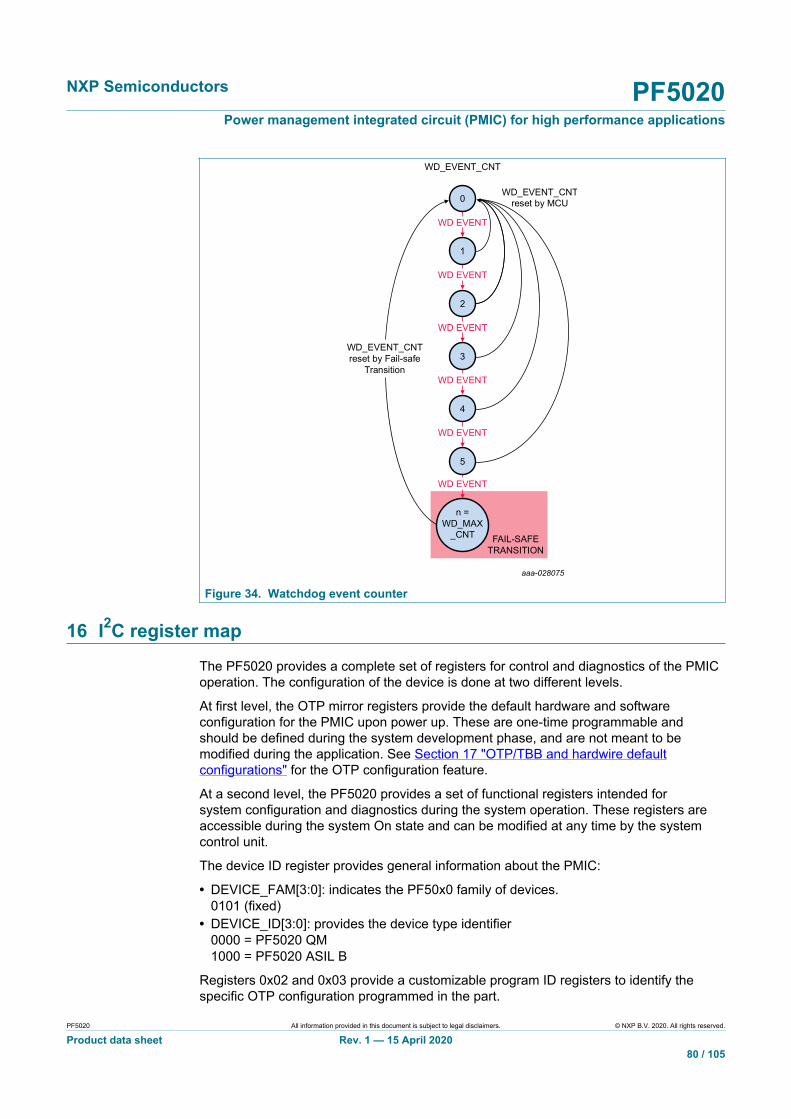
NXP Semiconductors PF5020Power management integrated circuit (PMIC) for high performance applications
PF5020 All information provided in this document is subject to legal disclaimers. © NXP B.V. 2020. All rights reserved.
Product data sheet Rev. 1 — 15 April 202080 / 105
WD_EVENT_CNTreset by Fail-safe
Transition
WD_EVENT_CNTreset by MCU
aaa-028075
WD_EVENT_CNT
WD EVENT
WD EVENT
WD EVENT
WD EVENT
WD EVENT
WD EVENT
FAIL-SAFETRANSITION
n =WD_MAX
_CNT
5
4
3
2
1
0
Figure 34. Watchdog event counter
16 I2C register map
The PF5020 provides a complete set of registers for control and diagnostics of the PMICoperation. The configuration of the device is done at two different levels.
At first level, the OTP mirror registers provide the default hardware and softwareconfiguration for the PMIC upon power up. These are one-time programmable andshould be defined during the system development phase, and are not meant to bemodified during the application. See Section 17 "OTP/TBB and hardwire defaultconfigurations" for the OTP configuration feature.
At a second level, the PF5020 provides a set of functional registers intended forsystem configuration and diagnostics during the system operation. These registers areaccessible during the system On state and can be modified at any time by the systemcontrol unit.
The device ID register provides general information about the PMIC:
• DEVICE_FAM[3:0]: indicates the PF50x0 family of devices.0101 (fixed)
• DEVICE_ID[3:0]: provides the device type identifier0000 = PF5020 QM1000 = PF5020 ASIL B
Registers 0x02 and 0x03 provide a customizable program ID registers to identify thespecific OTP configuration programmed in the part.

NXP Semiconductors PF5020Power management integrated circuit (PMIC) for high performance applications
PF5020 All information provided in this document is subject to legal disclaimers. © NXP B.V. 2020. All rights reserved.
Product data sheet Rev. 1 — 15 April 202081 / 105
• EMREV (Address 0x02): contains the MSB bits PROG_ID[8:11]• PROG_ID (Address 0x03): contains the LSB bit PROG_ID[7:0]
16.1 PF5020 OTP mirror register map
Reset types
OFF_OTP Register loads the OTP mirror register values during power up
OTP Register available in OTP bank only, Reset From fuses when VIN crosses UVDET threshold
VSNVS Reset when BOS has no valid input (VIN < UVDET --> VSNVS not present)
MRADDR
FUSEADDR
Register name BIT7 BIT6 BIT5 BIT4 BIT3 BIT2 BIT1 BIT0
A0 0 OTP I2C — — — OTP_I2C_SECURE_EN
OTP_I2C_CRC_EN OTP_I2C_ADD[2:0]
A1 1 OTP CTRL1 — — OTP_EWARN_TIME[1:0] OTP_FS_BYPASS OTP_STANDBYINV OTP_PG_ACTIVE OTP_PG_CHECK
A2 2 OTP CTRL2 OTP_FSS_EN OTP_FSS_RANGE — OTP_XFAILB_EN OTP_VIN_OVLO_SDWN
OTP_VIN_OVLO_EN
OTP_VIN_OVLO_DBNC[1:0]
A3 3 OTP CTRL3 OTP_VTT_PDOWN OTP_SW2_VTTEN — — Reserved OTP_SW1CONFIG[1:0]
A4 4 OTP FREQCTRL
OTP_SW_MODE OTP_SYNC_MODE OTP_SYNCOUT_EN
OTP_FSYNC_RANGE
OTP_CLK_FREQ[3:0]
A5 5 OTP PWRON — — OTP_PWRON_MODE
OTP_PWRON_DBNC[1:0] OTP_PWRON_RST_EN
OTP_TRESET[1:0]
A6 6 OTP WDCONFIG
— — OTP_WDI_MODE OTP_WDI_INV OTP_WD_EN OTP_ WD_STBY_EN
OTP_WDI_STBY_ACTIVE
OTP_WDWINDOW
A7 7 OTP WDEXPIRE
— — — — — OTP_WD_MAX_EXPIRE[2:0]
A8 8 OTP WDCOUNTER
OTP_WD_DURATION[3:0] OTP_WD_MAX_CNT [3:0]
A9 9 OTP FAULTCOUNTERS
OTP_FS_MAX_CNT[3:0] OTP_FAULT_MAX_CNT[3:0]
AA A OTP FAULTTIMERS
— OTP_FS_OK_TIMER[2:0] OTP_TIMER_FAULT[3:0]
AB B OTP PWRDNDLY1
OTP_GRP4_DLY[1:0] OTP_GRP3_DLY[1:0] OTP_GRP2_DLY[1:0] OTP_GRP1_DLY[1:0]
AC C OTP PWRDNDLY2
OTP_PD_SEQ_DLY[1:0] — — — — OTP_RESETBMCU_DLY[1:0]
AD D OTP PWRUPCTRL
— OTP_PWRDWN_MODE
OTP_PGOOD_PDGRP[1:0] OTP_RESETBMCU_PDGRP[1:0] OTP_SEQ_TBASE[1:0]
AE E OTPRESETBMCUPWRUP
OTP_RESETBMCU_SEQ[7:0]
AF F OTP PGOODPWRUP
OTP_PGOOD_SEQ[7:0]
B0 10 OTP SW1VOLT
OTP_VSW1[7:0]
B1 11 OTP SW1PWRUP
OTP_SW1_SEQ[7:0]
B2 12 OTP SW1CONFIG1
OTP_SW1UV_TH[1:0] OTP_SW1OV_TH[1:0] OTP_SW1_PDGRP[1:0] OTP_SW1ILIM[1:0]
B3 13 OTP SW1CONFIG2
OTP_SW1_LSELECT[1:0] OTP_SW1PHASE[2:0] — OTP_SW1_PG_EN OTP_SW1_WDBYPASS
B4 14 OTP SW2VOLT
OTP_VSW2[7:0]
B5 15 OTP SW2PWRUP
OTP_SW2_SEQ[7:0]
B6 16 OTP SW2CONFIG1
OTP_SW2UV_TH[1:0] OTP_SW2OV_TH[1:0] OTP_SW2_PDGRP[1:0] OTP_SW2ILIM[1:0]
B7 17 OTP SW2CONFIG2
OTP_SW2_LSELECT[1:0] OTP_SW2PHASE[2:0] — OTP_SW2_PG_EN OTP_SW2_WDBYPASS
B8 18 OTP SW3_VOLT
Reserved
B9 19 OTP SW3PWRUP
Reserved
BA 1A OTP SW3CONFIG1
Reserved Reserved Reserved Reserved
BB 1B OTP SW3CONFIG2
Reserved Reserved — Reserved Reserved
BC 1C OTP SW4VOLT
Reserved
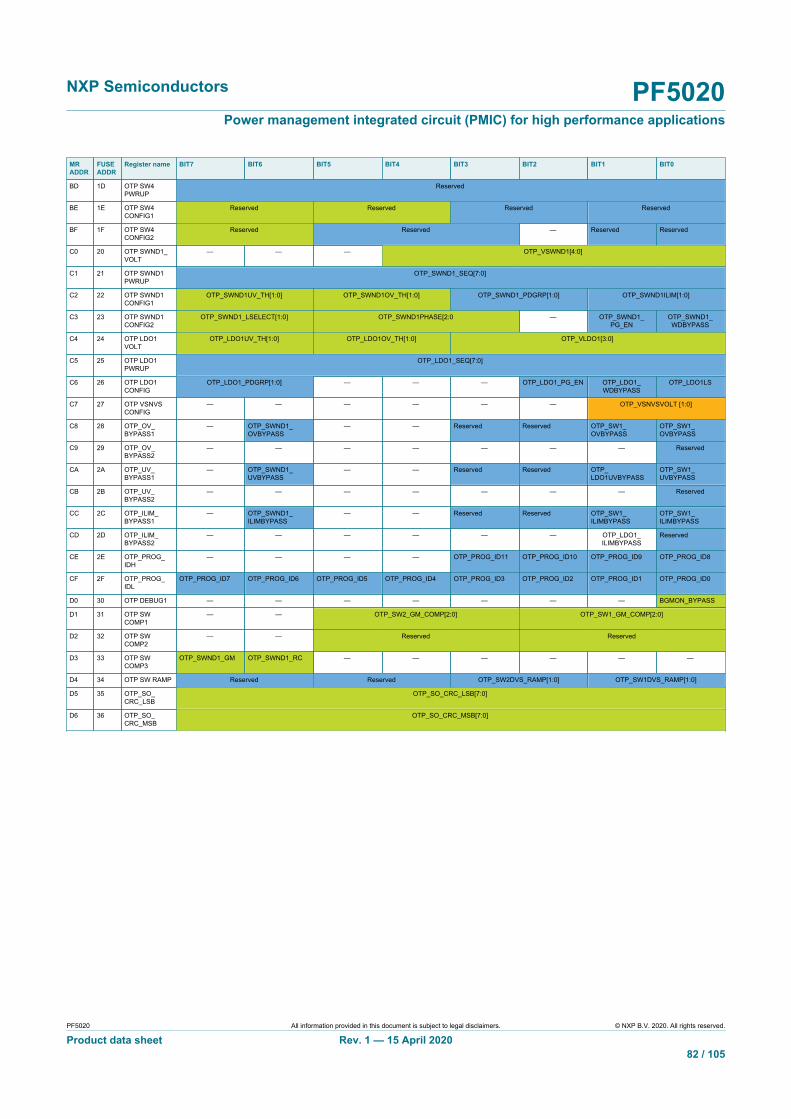
NXP Semiconductors PF5020Power management integrated circuit (PMIC) for high performance applications
PF5020 All information provided in this document is subject to legal disclaimers. © NXP B.V. 2020. All rights reserved.
Product data sheet Rev. 1 — 15 April 202082 / 105
MRADDR
FUSEADDR
Register name BIT7 BIT6 BIT5 BIT4 BIT3 BIT2 BIT1 BIT0
BD 1D OTP SW4PWRUP
Reserved
BE 1E OTP SW4CONFIG1
Reserved Reserved Reserved Reserved
BF 1F OTP SW4CONFIG2
Reserved Reserved — Reserved Reserved
C0 20 OTP SWND1_VOLT
— — — OTP_VSWND1[4:0]
C1 21 OTP SWND1PWRUP
OTP_SWND1_SEQ[7:0]
C2 22 OTP SWND1CONFIG1
OTP_SWND1UV_TH[1:0] OTP_SWND1OV_TH[1:0] OTP_SWND1_PDGRP[1:0] OTP_SWND1ILIM[1:0]
C3 23 OTP SWND1CONFIG2
OTP_SWND1_LSELECT[1:0] OTP_SWND1PHASE[2:0 — OTP_SWND1_PG_EN
OTP_SWND1_WDBYPASS
C4 24 OTP LDO1VOLT
OTP_LDO1UV_TH[1:0] OTP_LDO1OV_TH[1:0] OTP_VLDO1[3:0]
C5 25 OTP LDO1PWRUP
OTP_LDO1_SEQ[7:0]
C6 26 OTP LDO1CONFIG
OTP_LDO1_PDGRP[1:0] — — — OTP_LDO1_PG_EN OTP_LDO1_WDBYPASS
OTP_LDO1LS
C7 27 OTP VSNVSCONFIG
— — — — — — OTP_VSNVSVOLT [1:0]
C8 28 OTP_OV_BYPASS1
— OTP_SWND1_OVBYPASS
— — Reserved Reserved OTP_SW1_OVBYPASS
OTP_SW1_OVBYPASS
C9 29 OTP_OV_BYPASS2
— — — — — — — Reserved
CA 2A OTP_UV_BYPASS1
— OTP_SWND1_UVBYPASS
— — Reserved Reserved OTP_LDO1UVBYPASS
OTP_SW1_UVBYPASS
CB 2B OTP_UV_BYPASS2
— — — — — — — Reserved
CC 2C OTP_ILIM_BYPASS1
— OTP_SWND1_ILIMBYPASS
— — Reserved Reserved OTP_SW1_ILIMBYPASS
OTP_SW1_ILIMBYPASS
CD 2D OTP_ILIM_BYPASS2
— — — — — — OTP_LDO1_ILIMBYPASS
Reserved
CE 2E OTP_PROG_IDH
— — — — OTP_PROG_ID11 OTP_PROG_ID10 OTP_PROG_ID9 OTP_PROG_ID8
CF 2F OTP_PROG_IDL
OTP_PROG_ID7 OTP_PROG_ID6 OTP_PROG_ID5 OTP_PROG_ID4 OTP_PROG_ID3 OTP_PROG_ID2 OTP_PROG_ID1 OTP_PROG_ID0
D0 30 OTP DEBUG1 — — — — — — — BGMON_BYPASS
D1 31 OTP SWCOMP1
— — OTP_SW2_GM_COMP[2:0] OTP_SW1_GM_COMP[2:0]
D2 32 OTP SWCOMP2
— — Reserved Reserved
D3 33 OTP SWCOMP3
OTP_SWND1_GM OTP_SWND1_RC — — — — — —
D4 34 OTP SW RAMP Reserved Reserved OTP_SW2DVS_RAMP[1:0] OTP_SW1DVS_RAMP[1:0]
D5 35 OTP_SO_CRC_LSB
OTP_SO_CRC_LSB[7:0]
D6 36 OTP_SO_CRC_MSB
OTP_SO_CRC_MSB[7:0]
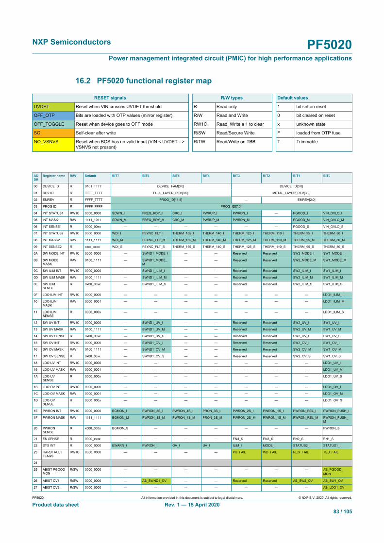
NXP Semiconductors PF5020Power management integrated circuit (PMIC) for high performance applications
PF5020 All information provided in this document is subject to legal disclaimers. © NXP B.V. 2020. All rights reserved.
Product data sheet Rev. 1 — 15 April 202083 / 105
16.2 PF5020 functional register map
RESET signals R/W types Default values
UVDET Reset when VIN crosses UVDET threshold R Read only 1 bit set on reset
OFF_OTP Bits are loaded with OTP values (mirror register) R/W Read and Write 0 bit cleared on reset
OFF_TOGGLE Reset when device goes to OFF mode RW1C Read, Write a 1 to clear x unknown state
SC Self-clear after write R/SW Read/Secure Write F loaded from OTP fuse
NO_VSNVS Reset when BOS has no valid input (VIN < UVDET -->VSNVS not present)
R/TW Read/Write on TBB T Trimmable
ADDR
Register name R/W Default BIT7 BIT6 BIT5 BIT4 BIT3 BIT2 BIT1 BIT0
00 DEVICE ID R 0101_TTTT DEVICE_FAM[3:0] DEVICE_ID[3:0]
01 REV ID R TTTT_TTTT FULL_LAYER_REV[3:0] METAL_LAYER_REV[3:0]
02 EMREV R FFFF_TTTT PROG_ID[11:8] — EMREV[2:0]
03 PROG ID R FFFF_FFFF PROG_ID[7:0]
04 INT STATUS1 RW1C 0000_0000 SDWN_I FREQ_RDY_I CRC_I PWRUP_I PWRDN_I — PGOOD_I VIN_OVLO_I
05 INT MASK1 R/W 1111_1011 SDWN_M FREQ_RDY_M CRC_M PWRUP_M PWRDN_M — PGOOD_M VIN_OVLO_M
06 INT SENSE1 R 0000_00xx — — — — — — PGOOD_S VIN_OVLO_S
07 INT STATUS2 RW1C 0000_0000 WDI_I FSYNC_FLT_I THERM_155_I THERM_140_I THERM_125_I THERM_110_I THERM_95_I THERM_80_I
08 INT MASK2 R/W 1111_1111 WDI_M FSYNC_FLT_M THERM_155_M THERM_140_M THERM_125_M THERM_110_M THERM_95_M THERM_80_M
09 INT SENSE2 R xxxx_xxxx WDI_S FSYNC_FLT_S THERM_155_S THERM_140_S THERM_125_S THERM_110_S THERM_95_S THERM_80_S
0A SW MODE INT RW1C 0000_0000 — SWND1_MODE_I — — Reserved Reserved SW2_MODE_I SW1_MODE_I
0B SW MODEMASK
R/W 0100_1111 — SWND1_MODE_M
— — Reserved Reserved SW2_MODE_M SW1_MODE_M
0C SW ILIM INT RW1C 0000_0000 — SWND1_ILIM_I — — Reserved Reserved SW2_ILIM_I SW1_ILIM_I
0D SW ILIM MASK R/W 0100_1111 — SWND1_ILIM_M — — Reserved Reserved SW2_ILIM_M SW1_ILIM_M
0E SW ILIMSENSE
R 0x00_00xx — SWND1_ILIM_S — — Reserved Reserved SW2_ILIM_S SW1_ILIM_S
0F LDO ILIM INT RW1C 0000_0000 — — — — — — — LDO1_ILIM_I
10 LDO ILIMMASK
R/W 0000_0001 — — — — — — — LDO1_ILIM_M
11 LDO ILIMSENSE
R 0000_000x — — — — — — — LDO1_ILIM_S
12 SW UV INT RW1C 0000_0000 — SWND1_UV_I — — Reserved Reserved SW2_UV_I SW1_UV_I
13 SW UV MASK R/W 0100_1111 — SWND1_UV_M — — Reserved Reserved SW2_UV_M SW1_UV_M
14 SW UV SENSE R 0x00_00xx — SWND1_UV_S — — Reserved Reserved SW2_UV_S SW1_UV_S
15 SW OV INT RW1C 0000_0000 — SWND1_OV_I — — Reserved Reserved SW2_OV_I SW1_OV_I
16 SW OV MASK R/W 0100_1111 — SWND1_OV_M — — Reserved Reserved SW2_OV_M SW1_OV_M
17 SW OV SENSE R 0x00_00xx — SWND1_OV_S — — Reserved Reserved SW2_OV_S SW1_OV_S
18 LDO UV INT RW1C 0000_0000 — — — — — — — LDO1_UV_I
19 LDO UV MASK R/W 0000_0001 — — — — — — — LDO1_UV_M
1A LDO UVSENSE
R 0000_000x — — — — — — — LDO1_UV_S
1B LDO OV INT RW1C 0000_0000 — — — — — — — LDO1_OV_I
1C LDO OV MASK R/W 0000_0001 — — — — — — — LDO1_OV_M
1D LDO OVSENSE
R 0000_000x — — — — — — — LDO1_OV_S
1E PWRON INT RW1C 0000_0000 BGMON_I PWRON_8S_I PWRON_4S_I PRON_3S_I PWRON_2S_I PWRON_1S_I PWRON_REL_I PWRON_PUSH_I
1F PWRON MASK R/W 1111_1111 BGMON_M PWRON_8S_M PWRON_4S_M PRON_3S_M PWRON_2S_M PWRON_1S_M PWRON_REL_M PWRON_PUSH_M
20 PWRONSENSE
R x000_000x BGMON_S — — — — — — PWRON_S
21 EN SENSE R 0000_xxxx — — — — EN4_S EN3_S EN2_S EN1_S
22 SYS INT R 0000_0000 EWARN_I PWRON_I OV_I UV_I ILIM_I MODE_I STATUS2_I STATUS1_I
23 HARDFAULTFLAGS
RW1C 0000_0000 — — — — PU_FAIL WD_FAIL REG_FAIL TSD_FAIL
24
25 ABIST PGOODMON
R/SW 0000_0000 — — — — — — — AB_PGOOD_MON
26 ABIST OV1 R/SW 0000_0000 — AB_SWND1_OV — — Reserved Reserved AB_SW2_OV AB_SW1_OV
27 ABIST OV2 R/SW 0000_0000 — — — — — — — AB_LDO1_OV
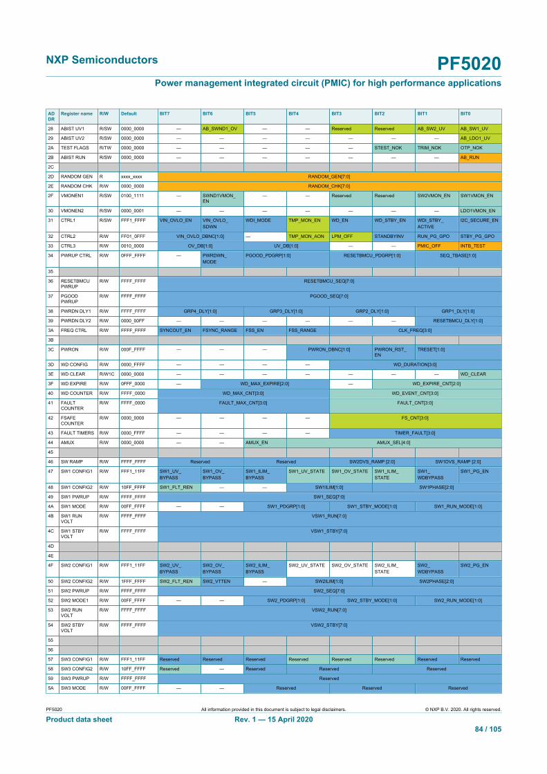
NXP Semiconductors PF5020Power management integrated circuit (PMIC) for high performance applications
PF5020 All information provided in this document is subject to legal disclaimers. © NXP B.V. 2020. All rights reserved.
Product data sheet Rev. 1 — 15 April 202084 / 105
ADDR
Register name R/W Default BIT7 BIT6 BIT5 BIT4 BIT3 BIT2 BIT1 BIT0
28 ABIST UV1 R/SW 0000_0000 — AB_SWND1_OV — — Reserved Reserved AB_SW2_UV AB_SW1_UV
29 ABIST UV2 R/SW 0000_0000 — — — — — — — AB_LDO1_UV
2A TEST FLAGS R/TW 0000_0000 — — — — — STEST_NOK TRIM_NOK OTP_NOK
2B ABIST RUN R/SW 0000_0000 — — — — — — — AB_RUN
2C
2D RANDOM GEN R xxxx_xxxx RANDOM_GEN[7:0]
2E RANDOM CHK R/W 0000_0000 RANDOM_CHK[7:0]
2F VMONEN1 R/SW 0100_1111 — SWND1VMON_EN
— — Reserved Reserved SW2VMON_EN SW1VMON_EN
30 VMONEN2 R/SW 0000_0001 — — — — — — — LDO1VMON_EN
31 CTRL1 R/SW FFF1_FFFF VIN_OVLO_EN VIN_OVLO_SDWN
WDI_MODE TMP_MON_EN WD_EN WD_STBY_EN WDI_STBY_ACTIVE
I2C_SECURE_EN
32 CTRL2 R/W FF01_0FFF VIN_OVLO_DBNC[1:0] — TMP_MON_AON LPM_OFF STANDBYINV RUN_PG_GPO STBY_PG_GPO
33 CTRL3 R/W 0010_0000 OV_DB[1:0] UV_DB[1:0] — — PMIC_OFF INTB_TEST
34 PWRUP CTRL R/W 0FFF_FFFF — PWRDWN_MODE
PGOOD_PDGRP[1:0] RESETBMCU_PDGRP[1:0] SEQ_TBASE[1:0]
35
36 RESETBMCUPWRUP
R/W FFFF_FFFF RESETBMCU_SEQ[7:0]
37 PGOODPWRUP
R/W FFFF_FFFF PGOOD_SEQ[7:0]
38 PWRDN DLY1 R/W FFFF_FFFF GRP4_DLY[1:0] GRP3_DLY[1:0] GRP2_DLY[1:0] GRP1_DLY[1:0]
39 PWRDN DLY2 R/W 0000_00FF — — — — — — RESETBMCU_DLY[1:0]
3A FREQ CTRL R/W FFFF_FFFF SYNCOUT_EN FSYNC_RANGE FSS_EN FSS_RANGE CLK_FREQ[3:0]
3B
3C PWRON R/W 000F_FFFF — — — PWRON_DBNC[1:0] PWRON_RST_EN
TRESET[1:0]
3D WD CONFIG R/W 0000_FFFF — — — — WD_DURATION[3:0]
3E WD CLEAR R/W1C 0000_0000 — — — — — — — WD_CLEAR
3F WD EXPIRE R/W 0FFF_0000 — WD_MAX_EXPIRE[2:0] — WD_EXPIRE_CNT[2:0]
40 WD COUNTER R/W FFFF_0000 WD_MAX_CNT[3:0] WD_EVENT_CNT[3:0]
41 FAULTCOUNTER
R/W FFFF_0000 FAULT_MAX_CNT[3:0] FAULT_CNT[3:0]
42 FSAFECOUNTER
R/W 0000_0000 — — — — FS_CNT[3:0]
43 FAULT TIMERS R/W 0000_FFFF — — — — TIMER_FAULT[3:0]
44 AMUX R/W 0000_0000 — — AMUX_EN AMUX_SEL[4:0]
45
46 SW RAMP R/W FFFF_FFFF Reserved Reserved SW2DVS_RAMP [2:0] SW1DVS_RAMP [2:0]
47 SW1 CONFIG1 R/W FFF1_11FF SW1_UV_BYPASS
SW1_OV_BYPASS
SW1_ILIM_BYPASS
SW1_UV_STATE SW1_OV_STATE SW1_ILIM_STATE
SW1_WDBYPASS
SW1_PG_EN
48 SW1 CONFIG2 R/W 10FF_FFFF SW1_FLT_REN — — SW1ILIM[1:0] SW1PHASE[2:0]
49 SW1 PWRUP R/W FFFF_FFFF SW1_SEQ[7:0]
4A SW1 MODE R/W 00FF_FFFF — — SW1_PDGRP[1:0] SW1_STBY_MODE[1:0] SW1_RUN_MODE[1:0]
4B SW1 RUNVOLT
R/W FFFF_FFFF VSW1_RUN[7:0]
4C SW1 STBYVOLT
R/W FFFF_FFFF VSW1_STBY[7:0]
4D
4E
4F SW2 CONFIG1 R/W FFF1_11FF SW2_UV_BYPASS
SW2_OV_BYPASS
SW2_ILIM_BYPASS
SW2_UV_STATE SW2_OV_STATE SW2_ILIM_STATE
SW2_WDBYPASS
SW2_PG_EN
50 SW2 CONFIG2 R/W 1FFF_FFFF SW2_FLT_REN SW2_VTTEN — SW2ILIM[1:0] SW2PHASE[2:0]
51 SW2 PWRUP R/W FFFF_FFFF SW2_SEQ[7:0]
52 SW2 MODE1 R/W 00FF_FFFF — — SW2_PDGRP[1:0] SW2_STBY_MODE[1:0] SW2_RUN_MODE[1:0]
53 SW2 RUNVOLT
R/W FFFF_FFFF VSW2_RUN[7:0]
54 SW2 STBYVOLT
R/W FFFF_FFFF VSW2_STBY[7:0]
55
56
57 SW3 CONFIG1 R/W FFF1_11FF Reserved Reserved Reserved Reserved Reserved Reserved Reserved Reserved
58 SW3 CONFIG2 R/W 10FF_FFFF Reserved — Reserved Reserved Reserved
59 SW3 PWRUP R/W FFFF_FFFF Reserved
5A SW3 MODE R/W 00FF_FFFF — — Reserved Reserved Reserved

NXP Semiconductors PF5020Power management integrated circuit (PMIC) for high performance applications
PF5020 All information provided in this document is subject to legal disclaimers. © NXP B.V. 2020. All rights reserved.
Product data sheet Rev. 1 — 15 April 202085 / 105
ADDR
Register name R/W Default BIT7 BIT6 BIT5 BIT4 BIT3 BIT2 BIT1 BIT0
5B SW3 RUNVOLT
R/W FFFF_FFFF Reserved
5C SW3 STBYVOLT
R/W FFFF_FFFF Reserved
5D
5E
5F SW4 CONFIG1 R/W FFF1_11FF Reserved Reserved Reserved Reserved Reserved Reserved Reserved Reserved
60 SW4 CONFIG2 R/W 10FF_FFFF Reserved — — Reserved Reserved
61 SW4 PWRUP R/W FFFF_FFFF Reserved
62 SW4 MODE R/W 00FF_FFFF — — Reserved Reserved Reserved
63 SW4 RUNVOLT
R/W FFFF_FFFF Reserved
64 SW4 STBYVOLT
R/W FFFF_FFFF Reserved
65
66
67 SWND1CONFIG1
R/W FFF1_11FF SWND1_UV_BYPASS
SWND1_OV_BYPASS
SWND1_ILIM_BYPASS
SWND1_UV_STATE
SWND1_OV_STATE
SWND1_ILIM_STATE
SWND1_WDBYPASS
SWND1_PG_EN
68 SWND1CONFIG2
R/W 100F_FFFF SWND1_FLT_REN
— — SWND1ILIM[1:0] SWND1PHASE[2:0]
69 SWND1PWRUP
R/W FFFF_FFFF SWND1_SEQ[7:0]
6A SWND1MODE1
R/W 00FF_FFFF — — SWND1_PDGRP[1:0] SWND1_STBY_MODE[1:0] SWND1_RUN_MODE[1:0]
6B SWND1 RUNVOLT
R/W 000F_FFFF — — — VSWND1[4:0]
6C
6D
6E LDO1 CONFIG1 R/W FFF1_11FF LDO1_UV_BYPASS
LDO1_OV_BYPASS
LDO1_ILIM_BYPASS
LDO1_UV_STATE
LDO1_OV_STATE
LDO1_ILIM_STATE
DO1_WDBYPASS
LDO1_PG_EN
6F LDO1 CONFIG2 R/W 1FF0_00FF LDO1_FLT_REN LDO1_PDGRP[1:0] — — — LDO1_RUN_EN LDO1_STBY_EN
70 LDO1 PWRUP R/W FFFF_FFFF LDO1_SEQ[7:0]
71 LDO1 RUNVOLT
R/W 0000_FFFF — — — — VLDO1_RUN[3:0]
72 LDO1 STBYVOLT
R/W 0000_FFFF — — — — VLDO1_STBY[3:0]
73
74
75 VSNVSCONFIG1
R/W 0000_00FF — — — — — — VSNVSVOLT [1:0]
76
77 PAGE SELECT R/TW 0000_0000 — — — — — PAGE[2:0]
17 OTP/TBB and hardwire default configurations
The PF5020 supports OTP fuse bank configuration and a predefined hardwireconfiguration to select the default power up configuration via the VDDOTP pin.
The default power up configuration is loaded into the functional I2C registers based onthe voltage on VDDOTP pin on register loading.
• If VDDOTP = GND, the device loads the configuration from the OTP mirror registers.• If VDDOTP = V1P5D, the device loads the configuration from the default hardwire
configuration.
When OTP configuration is selected, the register loading occurs in two stages:
• In the first stage, the fuses are loaded in the OTP mirror registers each time VINcrosses the UVDET threshold in the rising edge.
• At the second stage, the data from the mirror registers are loaded into the functionalI2C registers for device operation.
When VDDOTP = GND, the mirror registers hold the default configuration to be used ona power-on event. The mirror registers can be modified during the TBB mode in order to

NXP Semiconductors PF5020Power management integrated circuit (PMIC) for high performance applications
PF5020 All information provided in this document is subject to legal disclaimers. © NXP B.V. 2020. All rights reserved.
Product data sheet Rev. 1 — 15 April 202086 / 105
test a custom power up configuration and/or burn the configuration into the OTP fuses togenerate a customized default power up configuration.
When VDDOTP = V1P5D, the I2C functional register will always be loaded from thehardwire configuration each time a default loading is required. Therefore, no TBBoperation is possible in this configuration.
In the event of a TRIM/OTP loading failure or a self-test failure, the corresponding faultflag is set and any PWRUP event is ignored until the flags are cleared by writing a 1during the QPU_OFF state.
The TRIM_NOK, OTP_NOK and STEST_NOK flags can only be written when theTBBEN = V1P5D (in TBB mode). In normal operation, the TRIM_NOK, OTP_NOK andSTEST_NOK flags can only be read, but not cleared.
17.1 TBB (Try Before Buy) operationThe PF5020 allows temporary configuration (TBB) to debug or test a customized powerup configuration in the system. In order to access the TBB mode, the TBBEN pin shouldbe pulled up to V1P5D.
In this mode of operation, the device ignores the default value of the LPM_OFF bit andmoves into the QPU_Off state, regardless of the result of the self-test. However, theactual result of the self-test is notified by the STEST_NOK flag.
• When the self-test is successful the STEST_NOK flag is set to 0.• When the self-test has failed, the STEST_NOK flag is set to 1.
In the TBB mode, the following conditions are valid:
• I2C communication uses standard communication with no CRC and secure writedisabled.
• Default I2C address is 0x08 regardless of the address configured by OTP.• Watchdog monitoring is disabled (including WDI and internal watchdog timer).• The PF5020 can communicate through I2C as long as VDDIO is provided to the PMIC
externally.
The PAGE[2:0] bits are provided to grant access to the mirror registers and other OTPdedicated bits. When the device is in the TBB mode, it can access the mirror registersin the extended register Page 1. With the TBBEN pin pulled low, access to the extendedregister pages is not allowed.
The mirror registers are preloaded with the values from the OTP configuration. Thesemay be modified to set the proper power up configuration during TBB operation.
If a power up event is present with the TBBEN pin pulled to V1P5D, the device will powerup with the proper configuration but limited functionality.
Limited functionality includes:
• Default I2C address = 0x08• CRC and secure write disabled• Watchdog operation/monitoring disable
In order to allow TBB operation with full functionality, the TBBEN pin must be low whenthe power up event occurs.
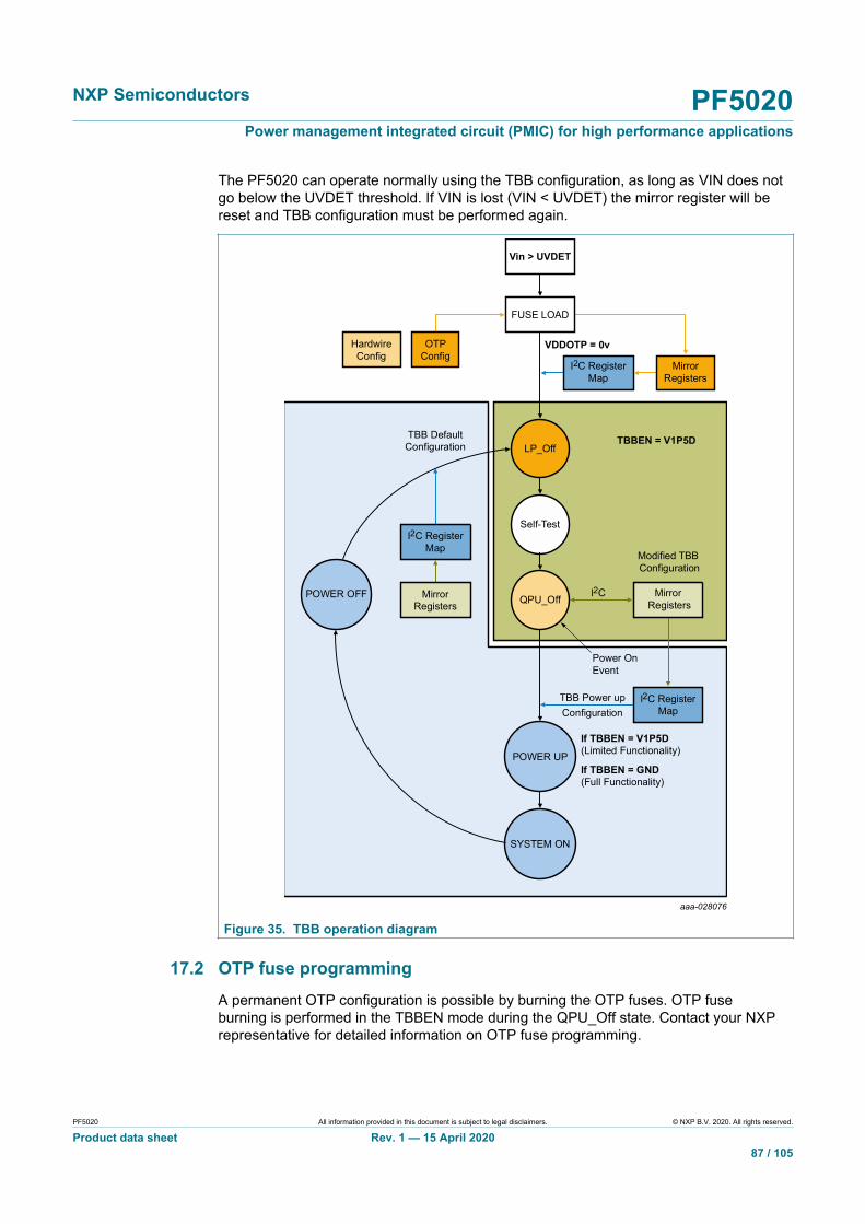
NXP Semiconductors PF5020Power management integrated circuit (PMIC) for high performance applications
PF5020 All information provided in this document is subject to legal disclaimers. © NXP B.V. 2020. All rights reserved.
Product data sheet Rev. 1 — 15 April 202087 / 105
The PF5020 can operate normally using the TBB configuration, as long as VIN does notgo below the UVDET threshold. If VIN is lost (VIN < UVDET) the mirror register will bereset and TBB configuration must be performed again.
aaa-028076
LP_Off
QPU_Off
Power OnEvent
Self-Test
l2C
POWER UP
POWER OFF
SYSTEM ON
MirrorRegisters
FUSE LOAD
Vin > UVDET
OTPConfig
HardwireConfig
I2C RegisterMap
TBB DefaultConfiguration
l2C RegisterMap
TBB Power up
lf TBBEN = V1P5D(Limited Functionality)
lf TBBEN = GND(Full Functionality)
Configuration
Modified TBBConfiguration
TBBEN = V1P5D
VDDOTP = 0v
I2C RegisterMap
MirrorRegisters
MirrorRegisters
Figure 35. TBB operation diagram
17.2 OTP fuse programmingA permanent OTP configuration is possible by burning the OTP fuses. OTP fuseburning is performed in the TBBEN mode during the QPU_Off state. Contact your NXPrepresentative for detailed information on OTP fuse programming.

NXP Semiconductors PF5020Power management integrated circuit (PMIC) for high performance applications
PF5020 All information provided in this document is subject to legal disclaimers. © NXP B.V. 2020. All rights reserved.
Product data sheet Rev. 1 — 15 April 202088 / 105
17.3 Default hardwire configurationIf VDDOTP = V1P5D, the device loads the configuration from the default hardwireconfiguration directly into the corresponding I2C functional registers each time theregisters need to be reloaded.
When using the hardwire configuration, the TRIM values are still loaded from the OTPfuses. In the event of a TRIM loading failure, the corresponding fault flag is set to 1.
When the hardwire configuration is used, the PF5020 does not allow TBB modeoperation. When TBBEN = V1P5D, the device enters a debug mode. In this mode ofoperation, the device ignores the default value of the LPM_OFF bit and moves into theQPU_Off state, regardless of the result of the self-test. However, the actual result of theself-test is notified by the STEST_NOK flag.
• When the self-test is successful, the STEST_NOK flag is set to 0• When the self-test has failed, the STEST_NOK flag is set to 1
During hardwire configuration, the OTP_NOK flag is always set to 0.
When any of the TRIM_NOK, OTP_NOK or STEST_NOK flags are set, any PWRUPevent is ignored until the flags are cleared by writing a 0. These flags can only be writtenwhen the system is in the debug mode, (TBBEN = V1P5D). In normal operation, theTRIM_NOK, OTP_NOK and STEST_NOK flags are read only.
NXP Semiconductors PF5020Power management integrated circuit (PMIC) for high performance applications
PF5020 All information provided in this document is subject to legal disclaimers. © NXP B.V. 2020. All rights reserved.
Product data sheet Rev. 1 — 15 April 202089 / 105
aaa-028077
LP_Off
QPU_Off
PWRONevent
PWRONevent
Self-Test
POWER UP
POWER OFF
SYSTEM ON
FUSE LOAD
Vin > UVDET
DefaultConfig
OTPConfig
I2C RegisterMap
TBB DefaultConfiguration
HardwirePower up Configuration
lf TBBEN = V1P5D(Limited Functionality)
lf TBBEN = GND(Full Functionality)
TBBEN = V1P5D· WDI disabled· Watchdog Disabled· l2C CRC disabled· l2C Address = 0x08· Access MiscellaneousDebug flags
VDDOTP = V1P5D
I2C RegisterMap
I2C RegisterMap
MirrorRegisters
MirrorRegisters
Figure 36. Hardwire operation diagram
For simplicity, the default hardwire configuration in PF5020 is organized based on theOTP register map as shown in Table 69.
Table 69. Default hardwire configurationADDR Register name BIT7 BIT6 BIT5 BIT4 BIT3 BIT2 BIT1 BIT0 Configuration
A0 OTP I2C 0 0 0 0 0 0 0 0 Secured I2C disabled | I2C CRC disabled | I2C address =0x08
A1 OTP CTRL1 0 0 0 0 0 0 1 0 EWARN_TIME = 100 µs | Fail-safe state enabled |STANDBY active high | PGOOD indicator | RESETBMCUis not influenced by power-up
A2 OTP CTRL2 0 0 0 0 0 1 0 1 XFAIL = disabled | VIN_OVLO shutdown disabled | VIN_OVLO enabled | VIN_OVLO debounce = 100 µs

NXP Semiconductors PF5020Power management integrated circuit (PMIC) for high performance applications
PF5020 All information provided in this document is subject to legal disclaimers. © NXP B.V. 2020. All rights reserved.
Product data sheet Rev. 1 — 15 April 202090 / 105
ADDR Register name BIT7 BIT6 BIT5 BIT4 BIT3 BIT2 BIT1 BIT0 Configuration
A3 OTP CTRL3 0 0 0 0 0 0 0 1 VTT pull down enabled | Dual phase: SW1/SW2
A4 OTP FREQ CTRL 0 0 0 0 0 0 0 0 SYNCIN = disabled | SYNCOUT disabled | SYNCIN range= 2 MHz to 3 MHz | CLK frequency = 2.5 MHz
A5 OTP PWRON 0 0 0 0 0 0 0 0 PWRON = Level sensitive
A6 OTP WD CONFIG 0 0 0 1 0 0 0 0 WDI generates soft WD reset | WDI detect on rising edge| WD timer disabled | WD timer in standby disabled |WDIdetect in standby disabled | WD Windows = 100 %
A7 OTP WD EXPIRE 0 0 0 0 0 1 1 1 Max WD expire count = 8
A8 OTP WD COUNTER 1 0 1 0 1 1 1 1 WD duration = 1024 ms | Max WD count = 16
A9 OTP FAULTCOUNTERS
1 1 1 1 1 1 1 1 Fail-safe MAX counter = 16 | Regulator fault Max Counter= 16
AA OTP FAULTTIMERS
0 0 0 0 1 1 1 1 Fail-safe OK timer = 1 minute | Regulator fault timer =disabled
AB OTP PWRDN DLY1 0 0 0 0 0 0 0 0 GRP4 delay = 125 µs | GRP 3 delay = 125 µs | GRP 2delay = 125 µs | GRP 1 delay = 125 µs
AC OTP PWRDN DLY2 0 0 0 0 0 0 0 1 Power Down Delay = 0 | RESETBMCU delay = 10 µs
AD OTP PWRUP CTRL 0 0 0 0 0 0 1 0 PD mirror sequence | RESETBMCU PD Group2 | TBASE =250 µs
AE OTP RESETBMCUPWRUP
0 0 0 0 0 1 1 1 RESETBMCU SEQ = Slot 6 (TBASE x 6 = 1500 µs)
AF OTP PGOODPWRUP
0 0 0 0 0 0 0 0 PGOOD SEQ = OFF
B0 OTP SW1 VOLT 0 1 1 0 0 0 0 0 Voltage = 1.0 V
B1 OTP SW1 PWRUP 0 0 0 0 0 0 0 1 SEQ = Slot 0
B2 OTP SW1 CONFIG1 0 1 0 1 0 0 1 1 UV mon = 7 % | OV mon = 7 % | SW PD Group4 | ILIM min3.1 A
B3 OTP SW1 CONFIG2 0 0 1 1 1 1 1 0 L = 1 µH | Phase = 0º | DVS Ramp = 12.5 mV/µs | PG = EN| WDBYPASS = disable
B4 OTP SW2 VOLT 0 1 1 0 0 0 0 0 Voltage = 1.0 V
B5 OTP SW2 PWRUP 0 0 0 0 0 0 0 1 SEQ = Slot 0
B6 OTP SW2 CONFIG1 0 1 0 1 0 0 1 1 UV mon = 7 % | OV mon = 7 % | SW PD Group4 | ILIM min3.1 A
B7 OTP SW2 CONFIG2 0 0 0 1 1 1 1 0 L = 1 µH | Phase = 180º | DVS Ramp = 12.5 mV/µs | PG =EN | WDBYPASS = disabled
B8 OTP SW3_VOLT 0 1 1 1 0 0 0 0 Voltage = 1.1 V
B9 OTP SW3 PWRUP 0 0 0 0 0 1 0 1 SEQ = Slot 4 (TBASE x 4 = 1000 µs)
BA OTP SW3 CONFIG1 0 1 0 1 0 0 1 1 UV mon = 7 % | OV mon = 7 % | SW PD Group4 | ILIM min3.1 A
C0 OTP SWND1 VOLT 0 0 0 1 0 1 0 1 Voltage = 3.3 V
C1 OTP SWND1PWRUP
0 0 0 0 0 0 1 1 SEQ = Slot 2 (TBASE x 2 = 500 µs)
C2 OTP SWND1CONFIG1
0 1 0 1 0 0 1 1 UV mon = 7 % | OV mon = 7 % | SW PD Group4 | ILIM min3.1 A
C3 OTP SWND1CONFIG2
0 0 1 1 1 0 1 0 L = 1 µH | Phase = 0º | PG = EN | WDBYPASS = disable
C4 OTP LDO1 VOLT 0 1 0 1 0 0 1 0 Voltage = 1.8 V
C5 OTP LDO1 PWRUP 0 0 0 0 0 0 0 1 SEQ = Slot 0
C6 OTP LDO1 CONFIG 0 0 0 0 0 1 0 0 LDO PD Group 4 | PG = EN | WDBYPASS = Disable | LDOmode
C7 OTP VSNVSCONFIG
0 0 0 0 0 0 1 0 Voltage = 3.0 V
C8 OTP_OV_BYPASS1 0 0 0 0 0 0 0 0 SWND1 and SWx OVBYPASS disabled
C9 OTP_OV_BYPASS2 0 0 0 0 0 0 0 0 LDO1 OVBYPASS disabled

NXP Semiconductors PF5020Power management integrated circuit (PMIC) for high performance applications
PF5020 All information provided in this document is subject to legal disclaimers. © NXP B.V. 2020. All rights reserved.
Product data sheet Rev. 1 — 15 April 202091 / 105
ADDR Register name BIT7 BIT6 BIT5 BIT4 BIT3 BIT2 BIT1 BIT0 Configuration
CA OTP_UV_BYPASS1 0 0 0 0 0 0 0 0 SWND1 and SWx UVBYPASS disabled
CB OTP_UV_BYPASS2 0 0 0 0 0 0 0 0 LDO1 UVBYPASS disabled
CC OTP_ILIM_BYPASS1
1 1 1 1 1 1 1 1 SWND1 and SWx ILIMBYPASS enabled
CD OTP_ILIM_BYPASS2
0 0 0 0 1 1 1 1 LDO1 ILIMBYPASS enabled
CE OTP_PROG_IDH 0 0 0 0 1 1 1 1 Default Program ID high Nibble = 0x0F
CF OTP_PROF_IDL 1 1 1 1 1 1 1 1 Default Program ID low Byte = 0xFF
D0 OTP DEBUG1 0 0 0 0 0 0 0 0 BG monitor disabled
D1 OTP SW COMP1 0 0 0 0 0 0 0 0 SW2 = 65GM | SW1 = 65GM
D3 OTP SW COMP3 0 0 0 0 0 0 0 0 SWND1 GM = 65, SWND1 RC = XX
D4 SW RAMP 0 0 0 0 0 0 0 0 SWxDVS_RAMP = 00
18 Functional safety
18.1 System safety strategyThe PF5020 is defined in a context of safety and shall provide a set of features toachieve the safety goals on such context. It provides a flexible yet complete safetyarchitecture to comply with ASIL B systems providing full programmability to enableor disable features to address the safety goal. This architecture includes protectivemechanisms to avoid unwanted modification on the respective safety features, asrequired by the system.
The following are features considered to be critical for the functional safety strategy:
• Internal watchdog timer• External watchdog monitoring input (WDI)• Output voltage monitoring with dedicated bandgap reference• Protected I2C protocol with CRC verification• Input overvoltage protection• Analog built-in self-test (ABIST)
18.2 Output voltage monitoring with dedicated bandgap referenceFor the type 2 buck regulator and LDOs, the OV/UV monitors operate from a dedicatedbandgap reference for voltage monitoring.
For the type 1 buck regulators, the OV/UV monitor operate from the same referenceas the regulator. To ensure the integrity of the type 1 buck regulators, a comparisonbetween the regulator bandgap and the monitoring bandgap is performed. A 5 % to12 % difference between the two bandgaps is an indicator of a potential regulation ormonitoring fault and is considered as a critical issue. Therefore, the device prevents theswitching regulators from powering up.
On the PF5020 ASIL B device, if a bandgap error is detected during a power up event,the self-test will fail and prevent the device from powering up regardless of the value ofthe OTP_BGMON_BYPASS bit.
During system On state, if a drift between two bandgaps is detected:
• When OTP_BGMON_BYPASS = 0, the power stage of the voltage regulators will beshutdown.

NXP Semiconductors PF5020Power management integrated circuit (PMIC) for high performance applications
PF5020 All information provided in this document is subject to legal disclaimers. © NXP B.V. 2020. All rights reserved.
Product data sheet Rev. 1 — 15 April 202092 / 105
• When OTP_BGMON_BYPASS = 1, The bandgap monitor only sends an interrupt tothe system to announce the bandgap failure.
The BGMON_I is asserted when a bandgap failure occurs, provided it is not masked.
The BGMON_S bit is set to 0 when the bandgaps are within range, and set to 1 when thebandgaps are out of range.
18.3 ABIST verificationThe PF5020 ASIL B implements an ABIST verification of all output voltage monitors aswell as PGOOD pin. The ABIST verification on the output voltage monitoring behaves asfollows:
• Device tests the OV comparators for each individual SWx and LDOx supply during theself-test routine
• Device tests the UV comparators for each individual SWx and LDOx supply during theself-test routine
• During the ABIST verification, it is required to ensure the corresponding OV/UVcomparators are able to toggle, which in turn is a sign of the integrity of these functions
• If any of the comparators is not able to toggle, a warning bit is set on the I2C registermap.– The ABIST_OV1 register contain the AB_SWx_OV bits for all external regulators.– The ABIST_OV2 register contain the AB_LDOx_OV bits for all external regulators.– The ABIST_UV1 register contain the AB_SWx_UV bits for all external regulators.– The ABIST_UV2 register contain the AB_LDOx_UV bits for all external regulators.
• The ABIST registers are cleared or overwritten each time the ABIST check isperformed.
• The ABIST registers are part of the secure registers and will require an I2C secure writeto be cleared if this feature is enabled.
Once ABIST check is performed, the PF5020 can proceed with the power up sequenceand the MCU should be able to request the value of these registers and learn if ABISTfailed for any of the voltage monitors.
The AB_RUN bit is provided to perform an ABIST verification on demand.
When the AB_RUN bit is set to 1, the control logic perform an ABIST verification on allOV/UV monitoring circuits. When the ABIST verification is finished, the AB_RUN bit self-clear to 0 and a new ABIST verification can be commanded as needed.
When the secure write feature is enabled, the system must perform a secure writesequence in order to start an ABIST verification on demand.
When the PF5020 performs an ABIST verification on demand, the OV/UV faultmonitoring is blanked for a maximum period of 200 µs. During this time, the system mustensure it is in a safe state, or it is safe to perform this action without violating the safetygoals of the system.
If a failure on the OV/UV monitor is detected during the ABIST on demand request,the PMIC will assert the corresponding ABIST flags. It is responsibility of the system toperform a diagnostic check after each ABIST verification to ensure it places the system insafe state if an ABIST fault is detected.

NXP Semiconductors PF5020Power management integrated circuit (PMIC) for high performance applications
PF5020 All information provided in this document is subject to legal disclaimers. © NXP B.V. 2020. All rights reserved.
Product data sheet Rev. 1 — 15 April 202093 / 105
19 IC level quiescent current requirementsTable 70. Quiescent current requirementsAll parameters are specified at TA = −40 to 125 °C, unless otherwise noted. Typical values are characterized at VIN = 5.0 Vand TA = 25 °C, unless otherwise noted.Symbol Parameter Min Typ Max Unit
ILPOFF LP_Off stateLPM_OFF = 0VIN > UVDETVSNVS = ON
—
40
150
µA
IQPUOFF QPU_OffLPM_OFF = 1System ready to power on
—
750
1000
µA
ISYSON System On core currentRun or standby and all regulators disabled
—
750
1000
µA
IFSAFE Fail-safe modeVIN > UVDETVSNVS = ON
—
40
150
µA

NXP Semiconductors PF5020Power management integrated circuit (PMIC) for high performance applications
PF5020 All information provided in this document is subject to legal disclaimers. © NXP B.V. 2020. All rights reserved.
Product data sheet Rev. 1 — 15 April 202094 / 105
20 Typical applications
aaa-030000
PF5020
toM
CU
toM
CU
toM
CU
toM
CU
toM
CU
from
MC
U
from
MC
U
from
MC
U
V1P5
A
VDD
IO
VDD
IO
VDD
IO
PGO
OD
x
RE
SETB
MC
U
PGO
OD
INTB
FAIL-SAFECONTROL
ENxSTATUS FLG from MCUENx
VDDOTP
TBBEN
WATCHDOGMONITORING
XFAI
LB
PWR
ON
STAN
DBY
WD
I
VDD
IO
4
WD TIMER
LOGICCONTROL
PGOOD
ABIST
PGOODMONITOR
4
100 kΩ100 kΩ100 kΩ100 kΩ100 kΩ
1 µH2 x 22 µF
4.7 µF
SW1FBVSW1
VIN
SW1OV/UV
MONITOR
TEMP SENSESW1
ABISTSW1LX
SW1IN
1 µH2 x 22 µF
4.7 µF
SW2FBVSW2
VIN
SW2OV/UV
MONITOR
TEMP SENSESW2
ABISTSW2LX
SW2IN
1 µH2 x 22 µF
4.7 µF
SWND1FBVSWND1
VIN
1.0 µF
VIN
SWND1OV/UV
MONITOR
TEMP SENSESWND1
TEMP SENSELDO1
ABISTSWND1LX
SWND1IN
LDO1OV/UV
MONITOR
LDO1OUT EPLDO1IN
ABIST
4.7 µF
2.2 µF
VIN
CLOCK MANAGEMENT100 KH CLOCK
20 MHz CLOCK +/-25 %SPREAD SPECTRUM
CLOCK SYNCHRONIZATION
20 MHz OSC DIAGNOSTIC
MUX
Syncin
I2C CONTROL
MIRRORREGISTERS
FUSE CRCVERIFICATION
OTP/TRIM
MEMORY FUNCTIONALREGISTERS
THERMALMONITOR
TEMPSENSE MAIN
SYNC
SDA
SCL
VDDIO
I2C DATA
I2C CLK
I/O supply(SWx/LDOx)
sync CLK
VSNVSVSNVS
functional block
functional safety block
VINVIN
Syncout
BANDGAPCOMPARATOR
BG2
VIN OVLO
UVDET
BG1
V1P5A POR
V1P5A
V1P5D
VSNVS
I2C CRC
V1P5D POR
IREF 2 IREF 11.0 µF
V1P5DV1P5D
1.0 µFV1P5A
V1P5A
GND
2.2 kΩ 2.2 kΩ
1.0 µF
LDO1OUT
Figure 37. Typical application diagram
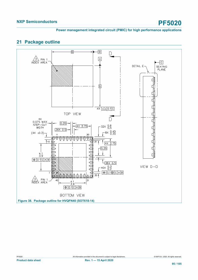
NXP Semiconductors PF5020Power management integrated circuit (PMIC) for high performance applications
PF5020 All information provided in this document is subject to legal disclaimers. © NXP B.V. 2020. All rights reserved.
Product data sheet Rev. 1 — 15 April 202095 / 105
21 Package outline
Figure 38. Package outline for HVQFN40 (SOT618-14)

NXP Semiconductors PF5020Power management integrated circuit (PMIC) for high performance applications
PF5020 All information provided in this document is subject to legal disclaimers. © NXP B.V. 2020. All rights reserved.
Product data sheet Rev. 1 — 15 April 202096 / 105
Figure 39. Package outline detail for HVQFN40 (SOT618-14)
Figure 40. Solder mask pattern for HVQFN40 (SOT618-14)
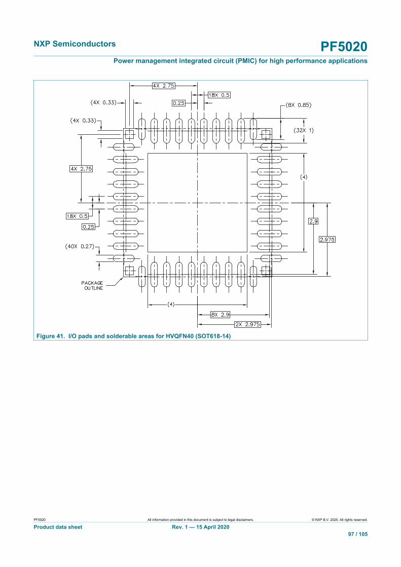
NXP Semiconductors PF5020Power management integrated circuit (PMIC) for high performance applications
PF5020 All information provided in this document is subject to legal disclaimers. © NXP B.V. 2020. All rights reserved.
Product data sheet Rev. 1 — 15 April 202097 / 105
Figure 41. I/O pads and solderable areas for HVQFN40 (SOT618-14)

NXP Semiconductors PF5020Power management integrated circuit (PMIC) for high performance applications
PF5020 All information provided in this document is subject to legal disclaimers. © NXP B.V. 2020. All rights reserved.
Product data sheet Rev. 1 — 15 April 202098 / 105
Figure 42. Solder paste stencil for HVQFN40 (SOT618-14)
Figure 43. Package outline notes for HVQFN40 (SOT618-14)

NXP Semiconductors PF5020Power management integrated circuit (PMIC) for high performance applications
PF5020 All information provided in this document is subject to legal disclaimers. © NXP B.V. 2020. All rights reserved.
Product data sheet Rev. 1 — 15 April 202099 / 105
22 Revision historyTable 71. Revision historyDocument ID Release
dateData sheet status Change
noticeSupersedes
PF5020 v.1.0 20200415 Product data sheet — —
NXP Semiconductors PF5020Power management integrated circuit (PMIC) for high performance applications
PF5020 All information provided in this document is subject to legal disclaimers. © NXP B.V. 2020. All rights reserved.
Product data sheet Rev. 1 — 15 April 2020100 / 105
23 Legal information
23.1 Data sheet status
Document status[1][2] Product status[3] Definition
Objective [short] data sheet Development This document contains data from the objective specification for productdevelopment.
Preliminary [short] data sheet Qualification This document contains data from the preliminary specification.
Product [short] data sheet Production This document contains the product specification.
[1] Please consult the most recently issued document before initiating or completing a design.[2] The term 'short data sheet' is explained in section "Definitions".[3] The product status of device(s) described in this document may have changed since this document was published and may differ in case of multiple
devices. The latest product status information is available on the Internet at URL http://www.nxp.com.
23.2 DefinitionsDraft — The document is a draft version only. The content is still underinternal review and subject to formal approval, which may result inmodifications or additions. NXP Semiconductors does not give anyrepresentations or warranties as to the accuracy or completeness ofinformation included herein and shall have no liability for the consequencesof use of such information.
Short data sheet — A short data sheet is an extract from a full data sheetwith the same product type number(s) and title. A short data sheet isintended for quick reference only and should not be relied upon to containdetailed and full information. For detailed and full information see therelevant full data sheet, which is available on request via the local NXPSemiconductors sales office. In case of any inconsistency or conflict with theshort data sheet, the full data sheet shall prevail.
Product specification — The information and data provided in a Productdata sheet shall define the specification of the product as agreed betweenNXP Semiconductors and its customer, unless NXP Semiconductors andcustomer have explicitly agreed otherwise in writing. In no event however,shall an agreement be valid in which the NXP Semiconductors productis deemed to offer functions and qualities beyond those described in theProduct data sheet.
23.3 DisclaimersLimited warranty and liability — Information in this document is believedto be accurate and reliable. However, NXP Semiconductors does notgive any representations or warranties, expressed or implied, as to theaccuracy or completeness of such information and shall have no liabilityfor the consequences of use of such information. NXP Semiconductorstakes no responsibility for the content in this document if provided by aninformation source outside of NXP Semiconductors. In no event shall NXPSemiconductors be liable for any indirect, incidental, punitive, special orconsequential damages (including - without limitation - lost profits, lostsavings, business interruption, costs related to the removal or replacementof any products or rework charges) whether or not such damages are basedon tort (including negligence), warranty, breach of contract or any otherlegal theory. Notwithstanding any damages that customer might incur forany reason whatsoever, NXP Semiconductors’ aggregate and cumulativeliability towards customer for the products described herein shall be limitedin accordance with the Terms and conditions of commercial sale of NXPSemiconductors.
Right to make changes — NXP Semiconductors reserves the right tomake changes to information published in this document, including withoutlimitation specifications and product descriptions, at any time and without
notice. This document supersedes and replaces all information supplied priorto the publication hereof.
Applications — Applications that are described herein for any of theseproducts are for illustrative purposes only. NXP Semiconductors makesno representation or warranty that such applications will be suitablefor the specified use without further testing or modification. Customersare responsible for the design and operation of their applications andproducts using NXP Semiconductors products, and NXP Semiconductorsaccepts no liability for any assistance with applications or customer productdesign. It is customer’s sole responsibility to determine whether the NXPSemiconductors product is suitable and fit for the customer’s applicationsand products planned, as well as for the planned application and use ofcustomer’s third party customer(s). Customers should provide appropriatedesign and operating safeguards to minimize the risks associated withtheir applications and products. NXP Semiconductors does not accept anyliability related to any default, damage, costs or problem which is basedon any weakness or default in the customer’s applications or products, orthe application or use by customer’s third party customer(s). Customer isresponsible for doing all necessary testing for the customer’s applicationsand products using NXP Semiconductors products in order to avoid adefault of the applications and the products or of the application or use bycustomer’s third party customer(s). NXP does not accept any liability in thisrespect.
Limiting values — Stress above one or more limiting values (as defined inthe Absolute Maximum Ratings System of IEC 60134) will cause permanentdamage to the device. Limiting values are stress ratings only and (proper)operation of the device at these or any other conditions above thosegiven in the Recommended operating conditions section (if present) or theCharacteristics sections of this document is not warranted. Constant orrepeated exposure to limiting values will permanently and irreversibly affectthe quality and reliability of the device.
Terms and conditions of commercial sale — NXP Semiconductorsproducts are sold subject to the general terms and conditions of commercialsale, as published at http://www.nxp.com/profile/terms, unless otherwiseagreed in a valid written individual agreement. In case an individualagreement is concluded only the terms and conditions of the respectiveagreement shall apply. NXP Semiconductors hereby expressly objects toapplying the customer’s general terms and conditions with regard to thepurchase of NXP Semiconductors products by customer.
No offer to sell or license — Nothing in this document may be interpretedor construed as an offer to sell products that is open for acceptance orthe grant, conveyance or implication of any license under any copyrights,patents or other industrial or intellectual property rights.
Suitability for use in automotive applications — This NXPSemiconductors product has been qualified for use in automotiveapplications. Unless otherwise agreed in writing, the product is not designed,authorized or warranted to be suitable for use in life support, life-critical orsafety-critical systems or equipment, nor in applications where failure ormalfunction of an NXP Semiconductors product can reasonably be expected
NXP Semiconductors PF5020Power management integrated circuit (PMIC) for high performance applications
PF5020 All information provided in this document is subject to legal disclaimers. © NXP B.V. 2020. All rights reserved.
Product data sheet Rev. 1 — 15 April 2020101 / 105
to result in personal injury, death or severe property or environmentaldamage. NXP Semiconductors and its suppliers accept no liability forinclusion and/or use of NXP Semiconductors products in such equipment orapplications and therefore such inclusion and/or use is at the customer's ownrisk.
Export control — This document as well as the item(s) described hereinmay be subject to export control regulations. Export might require a priorauthorization from competent authorities.
Translations — A non-English (translated) version of a document is forreference only. The English version shall prevail in case of any discrepancybetween the translated and English versions.
23.4 TrademarksNotice: All referenced brands, product names, service names andtrademarks are the property of their respective owners.
I2C-bus — logo is a trademark of NXP B.V.NXP — is a trademark of NXP B.V.
NXP Semiconductors PF5020Power management integrated circuit (PMIC) for high performance applications
PF5020 All information provided in this document is subject to legal disclaimers. © NXP B.V. 2020. All rights reserved.
Product data sheet Rev. 1 — 15 April 2020102 / 105
TablesTab. 1. Ordering information ..........................................2Tab. 2. Pin description ...................................................4Tab. 3. Absolute maximum ratings ................................5Tab. 4. ESD ratings ....................................................... 6Tab. 5. Thermal characteristics ..................................... 6Tab. 6. QFN40 thermal resistance and package
dissipation ratings ............................................. 6Tab. 7. Operating conditions ......................................... 6Tab. 8. Voltage supply summary ...................................8Tab. 9. Device differences .............................................8Tab. 10. State machine transition definition .................. 11Tab. 11. Fail-safe OK timer configuration ......................18Tab. 12. UVDET threshold ............................................ 18Tab. 13. VIN_OVLO debounce configuration ................ 19Tab. 14. VIN_OVLO specifications ................................19Tab. 15. Startup timing requirements (PWRON pulled
up) ................................................................... 20Tab. 16. Startup with PWRON driven high externally
and LPM_OFF = 0 .......................................... 21Tab. 17. Power up time base register ........................... 22Tab. 18. Power up sequence registers ..........................22Tab. 19. Power down regulator group bits .................... 26Tab. 20. Power down counter delay ..............................26Tab. 21. Programmable delay after RESETBMCU is
asserted ...........................................................26Tab. 22. Power down delay selection ............................27Tab. 23. Regulator control during fault event bits .......... 29Tab. 24. Fault timer register configuration .....................31Tab. 25. Fault bypass bits ............................................. 31Tab. 26. Interrupt registers ............................................ 36Tab. 27. I/O electrical specifications ..............................38Tab. 28. PWRON debounce configuration in edge
detection mode ................................................39Tab. 29. TRESET configuration .....................................39Tab. 30. Standby pin polarity control .............................40Tab. 31. PGOODx assignment ......................................42Tab. 32. ENx assignment .............................................. 43Tab. 33. I2C address configuration ............................... 46Tab. 34. Secure bits ...................................................... 48
Tab. 35. Internal supplies electrical characteristics ....... 49Tab. 36. VSNVS output voltage configuration ............... 50Tab. 37. VSNVS electrical characteristics ..................... 50Tab. 38. SWx ramp rates .............................................. 51Tab. 39. SWx output voltage configuration ....................52Tab. 40. SWx regulator mode configuration .................. 52Tab. 41. SWx current limit selection ..............................53Tab. 42. SWx phase configuration ................................ 53Tab. 43. SWx inductor selection bits .............................53Tab. 44. OTP_SW1CONFIG register description .......... 54Tab. 45. Type 1 buck regulator electrical
characteristics ..................................................54Tab. 46. Recommended external components ..............56Tab. 47. SWND1 output voltage configuration .............. 57Tab. 48. SWND1 regulator mode configuration .............58Tab. 49. SWND1 current limit selection ........................ 59Tab. 50. SWND1 phase configuration ...........................59Tab. 51. SWND1 inductor selection bits ........................59Tab. 52. Type 2 buck regulator electrical
characteristics ..................................................59Tab. 53. Recommended external components ..............61Tab. 54. LDO operation description .............................. 62Tab. 55. LDO output voltage configuration ....................62Tab. 56. LDO regulator electrical characteristics ...........63Tab. 57. UV threshold configuration register ................. 64Tab. 58. OV threshold configuration register .................65Tab. 59. UV debounce timer configuration ....................65Tab. 60. OV debounce timer configuration ....................65Tab. 61. VMON electrical characteristics ...................... 66Tab. 62. Manual frequency tuning configuration ............69Tab. 63. Clock management specifications ...................71Tab. 64. Thermal monitor specifications ........................73Tab. 65. Thermal monitor bit description .......................73Tab. 66. AMUX channel selection ................................. 74Tab. 67. Watchdog duration register ............................. 75Tab. 68. Soft WD register reset .....................................77Tab. 69. Default hardwire configuration .........................89Tab. 70. Quiescent current requirements ...................... 93Tab. 71. Revision history ...............................................99
FiguresFig. 1. Simplified application diagram ...........................2Fig. 2. Internal block diagram .......................................3Fig. 3. Pin configuration for 40-pin QFN .......................4Fig. 4. Functional block diagram .................................. 8Fig. 5. State diagram ..................................................10Fig. 6. Startup with PWRON pulled up .......................20Fig. 7. Startup with PWRON driven high externally
and bit LPM_OFF = 0 ..................................... 21Fig. 8. Power up/down sequence between Off and
system On state .............................................. 23Fig. 9. Power up/down sequence between run and
standby ............................................................24Fig. 10. Group power down sequence example ...........27
Fig. 11. Power down delay ...........................................28Fig. 12. Regulator turned off upon with RegX_
STATE = 0 and FLT_REN = 0 ........................ 29Fig. 13. Regulator turned off upon with RegX_
STATE = 0 and FLT_REN = 1 ........................ 30Fig. 14. Correct power up (no fault during power up) ....33Fig. 15. Power up sequencer with a temporary failure .. 34Fig. 16. Power up sequencer aborted as fault
persists for longer than 2.0 ms ........................35Fig. 17. I/O interface diagram .......................................37Fig. 18. XFAILB behavior during a power up
sequence .........................................................44

NXP Semiconductors PF5020Power management integrated circuit (PMIC) for high performance applications
PF5020 All information provided in this document is subject to legal disclaimers. © NXP B.V. 2020. All rights reserved.
Product data sheet Rev. 1 — 15 April 2020103 / 105
Fig. 19. XFAILB behavior during a power downsequence .........................................................45
Fig. 20. Behavior during an external XFAILB event ......45Fig. 21. External XFAILB event during a power up
sequence .........................................................46Fig. 22. 8 bit SAE J1850 CRC polynomial ................... 47Fig. 23. VSNVS block diagram .....................................49Fig. 24. Buck regulator block diagram ..........................51Fig. 25. Type 2 buck regulator block diagram .............. 57Fig. 26. LDO1 regulator block diagram ........................ 62Fig. 27. Voltage monitoring architecture .......................66Fig. 28. Clock management architecture ......................68Fig. 29. Spread-spectrum waveforms ...........................70Fig. 30. Thermal monitoring architecture ......................72Fig. 31. Watchdog timer operation ............................... 76Fig. 32. Soft WD reset behavior ...................................78
Fig. 33. Hard WD reset behavior ................................. 79Fig. 34. Watchdog event counter ................................. 80Fig. 35. TBB operation diagram ................................... 87Fig. 36. Hardwire operation diagram ............................89Fig. 37. Typical application diagram .............................94Fig. 38. Package outline for HVQFN40 (SOT618-14) ...95Fig. 39. Package outline detail for HVQFN40
(SOT618-14) ....................................................96Fig. 40. Solder mask pattern for HVQFN40
(SOT618-14) ....................................................96Fig. 41. I/O pads and solderable areas for HVQFN40
(SOT618-14) ....................................................97Fig. 42. Solder paste stencil for HVQFN40
(SOT618-14) ....................................................98Fig. 43. Package outline notes for HVQFN40
(SOT618-14) ....................................................98

NXP Semiconductors PF5020Power management integrated circuit (PMIC) for high performance applications
PF5020 All information provided in this document is subject to legal disclaimers. © NXP B.V. 2020. All rights reserved.
Product data sheet Rev. 1 — 15 April 2020104 / 105
Contents1 Overview .............................................................. 12 Features ............................................................... 13 Simplified application diagram .......................... 24 Ordering information .......................................... 25 Applications .........................................................36 Internal block diagram ........................................37 Pinning information ............................................ 47.1 Pinning ...............................................................47.2 Pin description ................................................... 48 Absolute maximum ratings ................................59 ESD ratings ..........................................................610 Thermal characteristics ......................................611 Operating conditions .......................................... 612 General description ............................................ 712.1 Features .............................................................712.2 Functional block diagram ...................................812.3 Power tree summary ......................................... 812.4 Device differences ............................................. 813 State machine ....................................................1013.1 State descriptions ............................................ 1313.1.1 OTP/TRIM load ................................................1313.1.2 LP_Off state .....................................................1313.1.3 Self-test routine (PF5020 ASIL B only) ............1313.1.4 QPU_Off state ................................................. 1413.1.5 Power up sequence .........................................1413.1.6 System On state ..............................................1413.1.6.1 Run state ......................................................... 1513.1.6.2 Standby state ...................................................1513.1.7 WD_Reset ........................................................1613.1.8 Power down state ............................................1713.1.9 Fail-safe transition ........................................... 1713.1.10 Fail-safe state (PF5020 ASIL B only) .............. 1714 General device operation ................................. 1814.1 UVDET .............................................................1814.2 VIN OVLO condition ........................................ 1814.3 IC startup timing with PWRON pulled up ......... 1914.4 IC startup timing with PWRON pulled low
during VIN application ..................................... 2014.5 Power up ......................................................... 2114.5.1 Power up events ..............................................2114.5.2 Power up sequencing ......................................2214.6 Power down .....................................................2414.6.1 Turn off events ................................................ 2414.6.2 Power down sequencing ................................. 2514.6.2.1 Sequential power down ................................... 2514.6.2.2 Group power down .......................................... 2514.6.2.3 Power down delay ........................................... 2714.7 Fault detection ................................................. 2814.7.1 Fault monitoring during power up state ............3214.8 Interrupt management ..................................... 3514.9 I/O interface pins ............................................. 3714.9.1 PWRON ........................................................... 3814.9.2 STANDBY ........................................................ 3914.9.3 RESETBMCU .................................................. 4014.9.4 INTB .................................................................4014.9.5 WDI ..................................................................40
14.9.6 PGOOD ............................................................4114.9.7 PGOODx ..........................................................4214.9.8 ENx .................................................................. 4214.9.9 TBBEN .............................................................4314.9.10 XFAILB .............................................................4314.9.11 SDA and SCL (I2C bus) .................................. 4614.9.11.1 I2C CRC verification ........................................4714.9.11.2 I2C secure write .............................................. 4715 Functional blocks ..............................................4915.1 Analog core and internal voltage references ....4915.2 VSNVS LDO/switch ......................................... 4915.3 Type 1 buck regulators (SW1 and SW2) ......... 5015.3.1 SW2 VTT operation .........................................5315.3.2 Multiphase operation ....................................... 5415.3.3 Electrical characteristics .................................. 5415.4 Type 2 buck regulator (SWND1) ..................... 5715.4.1 Electrical characteristics .................................. 5915.5 Linear regulator ............................................... 6115.5.1 LDO load switch operation .............................. 6315.5.2 LDO regulator electrical characteristics ........... 6315.6 Voltage monitoring ...........................................6415.6.1 Electrical characteristics .................................. 6615.7 Clock management ..........................................6715.7.1 Low frequency clock ........................................6815.7.2 High frequency clock ....................................... 6815.7.3 Manual frequency tuning ................................. 6815.7.4 Spread-spectrum ............................................. 6915.7.5 Clock synchronization ......................................7015.8 Thermal monitoring ..........................................7215.9 Analog multiplexer ........................................... 7415.10 Watchdog event management .........................7415.10.1 Internal watchdog timer ................................... 7415.10.2 Watchdog reset behaviors ...............................7716 I2C register map ................................................8016.1 PF5020 OTP mirror register map .................... 8116.2 PF5020 functional register map .......................8317 OTP/TBB and hardwire default
configurations ................................................... 8517.1 TBB (Try Before Buy) operation ...................... 8617.2 OTP fuse programming ................................... 8717.3 Default hardwire configuration ......................... 8818 Functional safety ...............................................9118.1 System safety strategy .................................... 9118.2 Output voltage monitoring with dedicated
bandgap reference ...........................................9118.3 ABIST verification ............................................ 9219 IC level quiescent current requirements .........9320 Typical applications ..........................................9421 Package outline .................................................9522 Revision history ................................................ 9923 Legal information ............................................ 100

NXP Semiconductors PF5020Power management integrated circuit (PMIC) for high performance applications
Please be aware that important notices concerning this document and the product(s)described herein, have been included in section 'Legal information'.
© NXP B.V. 2020. All rights reserved.For more information, please visit: http://www.nxp.comFor sales office addresses, please send an email to: [email protected]
Date of release: 15 April 2020Document identifier: PF5020