phase equilibria and semiconducting properties … bound... · r 380 reprintedfrom philips res....
TRANSCRIPT
R 380Reprinted from
Philips Res. Repts 14, 361-399, 1959.
PHASE EQUILIBRIA AND SEMICONDUCTINGPROPERTIES OF CADMIUM TELLURIDE *)
by D. de NOBEL546.48'241: 541.121 +537.311.33
Summary
In this thesis the relation is studied between the electrical and opticalproperties of single crystals of cadmium telluride and the conditions ofpreparation. The p-Tsx diagram of the system cadmium-tellurium isdescribed, showing the temperatures and Cd pressures of the maximummelting point and the melting point of stoichiometrie CdTe. The com-pound is purified by zone refining; foreign atoms are incorporated byzone levelling and single crystals are grown, which are reheated at vari-ous Cd pressures between 700 and 1000 °C, followed by quenching toroom temperature. On these samples conductivity and Hall measure-ments are performed at various temperatures, which lead to values ofthe concentration of charge carriers, of the ionization energies of thevarious centres and - for zr-type samples with shallow donors - of toedensity-of-state effective mass of the free electrons (mn*fm = 0·14 ±0'04). Thermo-electromotive force measurements of various /I and p-typesamples lead to values of the same effective mass for both types of car-rier, depending on the value adopted for the transport energy of elec-trons and holes (mn·fm = 0'13 - 0'066; mp·fm = 0·41 - 0·22). From ahydrogen-like model for the shallow donor an inertial effective mass forthe electrons of (mn·)' =0·147 is obtained. From optical transmissionmeasurements at various temperatures a value for the band gap of 1·50eV at room temperature and a temperature dependence of 2'34.10-4 to5.44.10-4 eVrK is found. Peaks in the spectra of photoluminescenceand photoconductivity can be correlated with a band-band transitionand with transitions between levels, caused by known centres, and oneof the bands. A theoretical discussion is presented of the various equi-libria which determine the state of CdTe at high temperature. By assum-ing a certain band scheme and values for the equilibrium constants,it is possible to calculate the concentrations of charge carriers and cen-tres at room temperature as a function of the Cd' pressure at which thecrystals were reheated. A qualitative comparison between the experimen-tal and various theoretical diagrams leads to the adoption of a definiteband scheme, in which two levels are ascribed to the cadmium vacancyand one to interstitial cadmium, to indium (as a specific donor) and togold (as a specific acceptor), respectively. From a quantitative discussionof the diagrams the values of some equilibrium constants are obtained,viz. the Frenkel constant Kp and the reduction constant Kr, describingthe equilibrium crystal-vapour. The temperature dependence of theseconstants leads to the energies required for the atomic processes involv-ed. Finally, the association effects which take place during the quenchingof activated samples are analyzed. In the appendix a discussion is givenof the type of bonding in CdTe.
Résumé
Dans cette thèse, on étudie Ie rapport entre les propriétés électriques etoptiques de monocristaux de tellurure de cadmium et les conditions depréparation. Le diagramme p-T-x du système cadmium-tellurium estdécrit en mentrant les températures et pressions de Cd au point de fusionmaximum et le point de fusion du CdTe stoechiométrique. Le mélange
------*) Thesis, University of Leyden, May 1958.'

2 D. de NOBEL
est purifié par raffinage par zone fondue; des atomes étrangers sont intro-duits par la méthode de zone-levelling et des monocristaux sont produitsqui sont réchauffés, à diverses pres sions de Cd, entre 700 et 10Q0°C avecrefroidissement rapide ensuite à Ia température ambiante. On effectuesur ces échantillóns des mesures de conductivité et du coefficient de Hallà diverses températures ce qui conduit à des valeurs de Ia concentrationdes porteurs de charge, des énergies d'ionisation des différents centreset - pour les échantillons du type 11 avec donneurs superficiels - de Iamasse effective"de la densité d'état des électrons Iibres (mn*lm = 0,14 ±0,04). Des mesures de la force thermo-électromotrice de divers échan-tiIIons des types 11 etp conduisent à des valeurs de Ia même masse effec-tive pour les deux types de porteurs, dépendant de la valeur adoptée pourl'énergie de transport des électrons et des trous (mn*lm = 0,13-0,066;mp* [m = 0,41-0,22). A partir d'un modèle du type hydrogène pour ledonneur superficiel, on obtient une masse effective d'inertie de (mn·)' =0,147 pour les électrons. En partant de mesures de transmission optiqueà diverses températures, on trouve pour l'intervalle de bande une valeurde 1,50 eV à la température ambiante et une sensibilité à la températurede 2,34.10-4 à 5,44.10-4 eVJOK. On peut établir une corrélation entre lescrêtes dans le spectre de la photoluminescence et de la photoconductivité .et la transition de bande à bande ainsi qu'avec les transitions entre lesniveaux, causées par des centres connus, et une des bandes. On présenteune discussion théorique des différents équilibres qui déterminent l'étatde CdTe à température élevée. En supposant une certaine répartitiondes niveaux et aussi des valeurs pour les constantes d'équilibre, i! estpossible de calculer les concentrations des porteurs de charge et descentres à la température ambiante en fonction de la pression de Cd àlaquelle ont été réchauffés les cristaux. Une comparaison qualitativeentre les diagrammes expérimentaux et divers diagrammes théoriquesconduit à l'adoption d'une répartition déterminée des niveaux, danslaquelle on attribue deux niveaux à la vacance de cadmium et un aucadmium interstitiel, à l'indium (comme donneur spécifique) et à l'or(comme accepteur spécifique) respectivement. Une étude quantitativedes diagrammes donne les valeurs de certaines constantes d'équilibre,à savoir la constante de Frenkel KF et Ia constante de réduction Kr quidécrit l'équilibre cristal-vapeur. La sensibilité à la température de cesconstantes conduit aux énergies nécessaires pour les processus atomiquesen question. Finalement, on analyse les effets d'association qui se pro-duisent pendant Ie refroidissement rapide des échantillons activés. Dansl'appendice, on traite du type de liaison dans Ie CdTe.
ZusammenfassungIn der vorliegenden Arbeit wird die Beziehung zwischen den elektrischenund optischen Eigenschaften von KadmiumteIlurid-EinkristaIlen undder vorausgegangenen Behandlung dieses Stoffes untersucht. D~sp-T-x-Diagramm des Systems Tellur-Kadmium wird unter Angabe der Tem-peraturen und Cd-Drucke des maximalen Schmelzpunktes sowie desSchmelzpunktes von stöchiometrischem CdTe beschrieben. Die Verbin-dung wird nach dem Zonenschmelzverfahren gereinigt; Fremdatomewerden durch Zonennivellierung eingebaut; ferner läBt man Einkristallewachsen, die bei verschiedenen Cd-Drucken zwischen 700 und 1000 °Cerhitzt werden, dem ein Abschrecken auf Zimmertemperatur folgt. Andiesen Proben werden Leitfähigkeits- und Halleffektmessungen bei ver-schiedenen Temperaturen durchgeführt, wodurch Werte der Ladungs-trägerkonzentration sowie die Ionisationsenergien der verschiedenenZentren und - für n-Proben mit flachen Donoren - die statistischeeffektive Masse des freien Elektrons (mn*lm = 0,14 ± 0,04) gefundenwerden. Messungen der Thermo-EMK bei verschiedenen 11- undp-Pro-ben liefern Werte der gleichen effektiven Masse für beide Trägertypen inAbhängigkeit von demjenigen Wert, der jeweils für die Transportenergieder Elektronen und Löcher zugrunde gelegt wurde (mn*lm = 0,13-0,066; mp*lm = 0,41-0,22). Anhand eines wasserstoffähnIichen ModelIs

PHASE EQUILIBRIA AND SEMICONDUCI'ING PROPERTIES OF CdTe 3
des'f1achen Donors wird eine effektive Trägheitsmasse des Elektrons von(mn*)' = 0,147 gefunden. Aus optischen Transmissionsmessungen beiverschiedenen Temperaturen wird für die Bandlücke ein Wert von1,50 eV bei Zimmertemperatur und eine Temperatur-abhängigkeit von2,34.10-4 bis 5,44.10-4 eVfOK gefunden. Maxima in den Spektren derPhotolumineszenz und Photoleitung können in eine Beziehung gebrachtwerden zu Band-Band-Übergängen und zu Übergängen zwischen ver-schiedenen Niveaus (verursacht durch bekannte Zentren) und einem detBänder. Eine theoretische Behandlung der verschiedenen Gleichgewichts-zustände welche den Zustand des CdTe bei hohen Temperaturen be-stimmen, wird dargelegt. Durch Annahme eines bestimmten Bandschemasund bestimmter Werte für die Gleichgewichtskonstanten können dieKonzentrationen der Ladungsträger und Zentren bei Zimmertemperaturals Funktion des Cd-Drucks, bei dem die KristalIe wiedererhitzt wurden,berechnet werden. Ein qualitativer Vergleich zwischen den experimen-tellen und den verschiedenen theoretischen Diagrammen führt zurAnnahme eines bestimmten Bandschemas, in dem zwei Niveaus derKadmiumleerstelle zugeschrieben werden, während ein Niveau deminterstitiellen Kadmium, Indium (als spezifischem Donor) bzw, Gold(als spezifischem Akzeptor) zugeschrieben wird. Aus einer quantitativenBetrachtung der Diagramme werden einige Gleichgewichtskonstantenerhalten, nämlich die Frenkelsche Konstante KF und die Reduktions-konstante Kr, welche das Gleichgewicht Kristall-Darnpf beschreibt. DieTemperaturabhängigkeit dieser Konstanten Iiefert die für die atomarenProzesse erforderlichen Energien. Abschliel3end werden die Assoziations-effekte untersucht, die während des Abschreckens von aktivierten Pro beneintreten. Im Anhang wird die Art der Bindung in CdTe beschrieben.
CONTENTS
INTRODUCTION
CHAPTER 1. EXPERIMENTAL PART
1.1. Preparation of CdTe1.2. The p-T-x diagram of CdTe1.3. Equilibrium CdTe (s) :;: CdTe (g) :;: Cd (g) + -§T~(g).1.4. Preparation of pure crystals and crystals with foreign atoms
1.4.1. Purification of CdTe1.4.2. Doping of CdTe.1.4.3. Growing of single crystals
1.5. Reheating of solid CdTe under pressures of one of the components1.6. Electrical measurements
1.6.1. Electric contacts1.6.2. Measurement of the thermoelectric power1.6.3. Measurement of the Hall effect1.6.4. Measurement of the resistance1.6.5. Measurement of the dielectric constant
1.7. Optical measurements1.7.1. Spectral transmission1.7.2. Electromotive force produced by irradiation of a CdTe p-n
. junction (photo-emf.)1.7.3. Emission of light
1.7.3.1. Emission of light from a rectifying s-n junction1.7.3.2. Photoluminescence
1.7.4. Photoconductivity1.7.5. Measurement of the refractive index

4 D. de NOBEL
CHAPTER 2. INTERPRETATION OF THE RESULTS OF THE ELECTRICALAND OPTICAL MEASUREMENTS
2.1. Interpretation of the measurements of the thermo-emf,2.2. Interpretatlon of the measurements of the Hall effect as a function of
the temperature2.2.1. 1I-Typesamples2.2.2. p-Type samples
2.3. Mobility of the charge carriers in CdTe2.4. Interpretation of the optical measurements
2.4.1. Transmission2.4.2. Photo-electromotive force2.4.3. Photoluminescence2.4.4. Photoconductivity
2.5. Characteristics of CdTe at room temperature
CHAPTER 3. THEORETICAL PART
3.1. Equilibria governing the state of the crystals at high temperature3.1.1. Native atomic disorder3.1.2. Native electronic disorder3.1.3. Atomic and electronic disorder caused by the incorporation of
foreign atoms,3.1.4. Reaction between the atmosphere and the crystal3.1.5. The complete equilibrium between the crystal and the vapour
at high temperatures3.1.5.1. Pure CdTe3.1.5.2. CdTe-In3.1.5.3. CdTe-Au
3.2. State of the crystals at room temperature3.3. Determination of the correct model3.4. Characteristic points in the concentratien-pressure graphs
3.4.1. Pure CdTe3.4.2. CdTe-In3.4.3. CdTe-Au
3.5. Determination of the equilibrium constants3.5.1. The intrinsic constant K,3.5.2. Determination of the equilibrium constants of the various
ionization processes3.5.3. The Frenkel equilibrium constant KF3.5.4. The equilibrium constant Kr3.5.5. Determination of K4 from the log 11 (or p) versus log PCd graphs
3.6. Comparison between theory and experiment3.6.1. Pure CdTe3.6.2. CdTe-In3.6.3. CdTe-Au and CdTe-Cu
3.7. Association and clustering effects3.7.1. Calculation of the association equilibrium3.7.2. Clustering effects in CdTe-In3.7.3. Anomalous effects in CdTe-Au
3.8. Calculation of the solidus curve in the T-x diagram3.9. Calculation of the energies involved in the transfer of cadmium between
crystal and vapour
APPENDIX. THE TYPE OF BONDING IN CdTe
PHASE EQUILmRIA AND SEMICONDUCTING PROPERTJES OF CdTc
INTRODUCTION
The electrical and optical properties of semiconductors depend on the presenceof small concentrations of crystal imperfections, which may be either vacanciesand interstitial atoms (so-called native imperfections) or foreign atoms. The con-centration of these imperfections is governed by the conditions prevailing duringthe preparation of-the crystals.In this thesis the relation between the conditions of preparation and the elec-
trical and optical properties will be discussed for CdTe.Cadmium telluride is a member of the series of compounds usually indicated
as the 2-6 compounds, which are compounds built up from elements of the 2ndand 6th sub-group of the periodic table. Of the other members of this group,ZnS has been studied intensively as a phosphor and CdS and CdSe have beenstudied as photoconductors. Yet various points are still open to discussion. Itis hoped that this study will not only lead to an insight in the properties of CdTeitself but that it mayalso aid in more fully understanding of other substances.The relation between the conditions of preparation and the concentration of
imperfections in a crystal has been put on a quantitative basis by the fundamentalwork of Schottky and Wagner 1)which was extended by Kröger, Vink and Vanden Boomgaard 2). These authors applied the theory to CdS and Bloem 3) appliedit to PbS.
Up to now only a small number of publications deal with CdTe. The earliermeasurements are restricted to the determination of the phase diagram 4) andthe optical properties of evaporated layers 5). The width of the band gap as afunction of the temperature was determined by Bube 6) from photoconductivitymeasurements. The influence of amounts of different foreign atoms on theelectrical properties ofpolycrystalline samples was studied by Jenny and Bube 7).Appels) measured the temperature dependence of the specificresistance of poly-crystalline samples and concluded to a transition from the sphalerite to thewurtzite structure at about 1000 "K. X-ray analysis up to 550 oe only showedthe sphalerite structure.In the following chapters first experimental results will be given regarding
preparation, phase diagram, Hall effect and specific resistance as a function ofthe temperature, Hall effect as a function of the atmosphere over the crystals atvarious values ofthe temperature, thermoelectric power, photoconductivity andluminescence (chapter 1). These results will be interpreted in chapter 2, leadingto values for the band gap and giving information about the position ofvarious
5

6 D. de NOBEL
donor and acceptor levels between the bands. In chapter 3 the equilibria govern-ing the state of the crystals at the temperature of preparation will be discussed.Knowledge of these equilibria enables us to calculate the state of the crystalsafter quenching to room temperature, which calculation is followed by a com-parison between calculated and experimental results. The deviations caused byassociation and clustering effectswill be considered here too. With the aid oftheequilibrium constants at high temperatures calculated in this chapter, the devia-tion from stoichiometry at the three-phase boundary (solidus curve in the T-xdiagram) can be calculated. The temperature dependence of some of these con-stants enables us to calculate energies involved in 'the exchange of cadmiumbetween crystal and vapour and in the transfer of cadmium from a lattice siteto an interstitial position.An estimate of the covalent and ionic character of CdTe will be given in an
appendix.

PHASE EQUILmRIA AND SEMICONDUCTING PROPER~ OF CdTc 7
CHAPTER 1
EXPERIMENTAL PART
1.1. Preparation of CdTe
CdTe was prepared from the elements. The cadmium and the tellurium usedcontained about 0·01% by weight of various impurities. The compound thusformed needed further purification which was carried out by the method ofzone melting 9).The preparation of CdTe is hindered by the fact that, although the reaction
between the elements already starts at 550°C, temperatures well above 800 "Care needed in order to get complete reaction. At such temperatures, however,CdTe tends to decompose markedly and no homogeneous phase will be obtainedif this decomposition is not prevented.This can be done in two ways. First, one can prepare CdTe from cadmium
and tellurium under a vapour pressure of one ofits components. Then the equili-brium
CdTe (s) ~ Cd (g) + tTe2 (g)
is shifted to the left and decomposition does not occur.It is also possible to carry out the reaction by which CdTe is formed under
a pressure of an inert gas. The latter method has been adopted by us. The appara-tus which was used is shown in fig. 1. It consists of a graphite crucible placedinside a silica container which in its turn is placed inside a pressure bomb, thewall of which is cooled. The crucible can be heated by means of a high-frequencyinduction coil also present inside the bomb. The silica container is closed witha stopper supplied with a tube ending at both sides in a capillary. The perforationof the stopper is necessary in order to make it possible to maintain equal pres-sures in and outside the crucible.The tube and the capillary have a double function. Firstly they slow down the
diffusion of cadmium and tellurium vapour out of the crucible. Secondly thevapour of the components still escaping from the crucible will condense in thewide section of the tube between the two capillaries which has a rather lowtemperature. This will prevent contamination of the bomb.
For the reaction an equimolecular mixture of cadmium and tellurium isbrought into the reaction vessel, a nitrogen pressure of about 50 atm is appliedand then the temperature is raised to about 600°C. The temperature is kept atthis level for 5minutes, after which the temperature is increased to a temperatureslightly above the melting point of CdTe (maximum melting point 1090 °C).

8 D. de NOBEL
0000000000000
94532
Fig. 1. Silica container CC) for the preparation of CdTe from a cadmium and tellurium mix-ture (A) contained in a graphite crucible CB). A high frequency coil (D) is used for heating.
After cooling down and letting off the pressure a mass of solid, polycrystallineCdTe is obtained.Although this method can be used to prepare a large amount (~ 400 g) of
CdTe in a rapid way, the growing of single crystals and the influencing of theircomposition is only possible by applying the other method, viz. by handling thematerial under definite pressures ofthe components. A first important questionwhich arises now is in which way the temperature, the composition of CdTe andthe partial pressures of its components are related to each other. Informationabout this question can be obtained by studyingthe equilibria between the variousphases in the system Cd-Te.
1.2. The P:T-x diagram of CdTe
The T-x diagram of the system Cd-Te was determined by Kobayashi 4) (fig. 2).The diagram is rather incomplete.In the first place no attention was paid to the exact coinposition of the solid
phases. In the second place only points of the liquidus curve corresponding tomixtures rich in tellurium were determined. The reason was that under the con-ditions at which Kobayashi worked, viz. in open 'crucibles in a stream ofC02,mixtures rich in cadmium tend to lose this cadmium very quickly and thereforedo not give reproducible results. In order to check Kobayashi's results and tosupplement them with points on the cadmium-rich side, some melting experi-ments were carried out in a closed and evacuated silica tube which was filled

PHASE EQUILIBRIA AND SEMICONDUCTING PROPERTIES OF CdTe
1100
700
../~ !l.--~ -, .1/" . I
I " -,i ~
I :
~
1\1,
m.p.(oe)
)900
500
20 40 60 80 10094533 --. % by weight of Te
Fig. 2. The T-x diagram of CdTe C. measurements of Kobayashi, • our measurements).
Fig. 3. Apparatus for the determination of the liquidus curve in the T-x diagram. CdTe CC)is contained in graphite crucible CB) enclosed by a silica container CD). A nichrome furnace CA)is used for heating. The temperature is measured by a thermocouple in D, the melting can beobserved through a hole in the furnace CF).
with mixtures of cadmium and tellurium of known composition. The tube wasfilled to such an extent that the amount of material present in the gas phase atthe melting temperature could be neglected (fig. 3).The mixture was completely molten, then slowly cooled down and by observ-
ing the surface ofthe liquid the point at which crystals started to appear was de-termined. This point was the point of the liquidus curve for the given composition.The accuracy of the measurements was approximately ± 2 oe. The results areshown in table I and fig. 2..As can be seen from this figure our results deviate from Kobayashi's results
for the reasons mentioned above. For tellurium-rich mixtures this deviation isrestricted to mixtures containing less than 60% by weight of tellurium. Ourmaximum melting pOÎI~.t(1090. "C) is higher than the value given by Kobayashi
9

10 D. de NOBEL
TABLE I
Melting points in the system cadmium-tellurium
% by weight of Te melting point COC)
10 88520 94030 97440 98345 100650 103653·2 109055 106860 102470 92680 840
(~ 1041 0C). For the cadmium-rich mixtures a sharp decrease of the meltingpoint can be observed within 5% deviation from the stoichiometrie composition(53.2%by weight of tellurium). For a larger excess of cadmium the melting pointdecreases gradually, falling again sharply when the composition approaches thepure cadmium side. The sharp drop near the stoichiometrie composition indi-cates a tendency of the liquid phase to separate into two phases: one with a com-position close to Cd :Te = 1: 1 and one which consists mainly of pure cadmium.Though less pronounced, the same phenomenon is also indicated by the.shapeofthe three-phase line in the p-T diagram (fig. 5), viz. close to the maximum melt-ing point at the cadmium-rich side.The T-x diagram is the projection ofthe three-phase blade on the T-x plane.
One can also study the p-T diagram which is the projection of the three-phaseblade. on the p-T plane.Whereas the first gives information regarding the composition in the three-
phase equilibria, the latter gives information regarding the corresponding pres-sures.. The p-T diagram can be determined by observing the temperature at whichCdTe in equilibrium with a definite cadmium or tellurium pressure starts to solidi-fy. The experiment was performed in a double-furnace system as shown in fig. 4.Byplacing CdTe at the left-hand side at a temperature Tl and a piece of cadmiummetal at the right-hand side at a temperature T2, the cadmium pressure overCdTe will be equal to the cadmium pressure corresponding to T2 if T2< Tl'As will be seen further on (section 1.3) this is only true if(PCd)T. is largerthan the

PHASE EQUILmRIA AND SEMICONDUCTING PROPERTIES OF CdT.
Fig. 4. Apparatus for the determination of the p-T diagram of CdTe. A graphite crucible (C)containing CdTe is enclosed in a silica tube (D) which is heated in a double-furnace system(A, B). The cadmium pressure is produced by a piece of cadmium metal (F). The temperaturesaremeasured by thermocouples in the tubes CE).
cadmium pressure of CdTe at the composition at which Ptotnl (= PCd+ P
Te.)
shows a minimum, provided that PCdTc is so low that it can be neglected.Maintaining a fixed cadmium pressure, the temperature Tl is increased until
melting of the CdTe occurs. Care must be taken that the condensed phases areinequilibrium with the cadmium pressure imposed. As the equilibrium liquid-gasis more readily established than the equilibrium solid-gas, the best procedure isas follows. First melt the CdTe completely and keep the melt for some time
la
PCd(atml
1
-.'0 ,.........
~-
.... .J~CdJpureCd-
1.~ <,'t
-'\ ~,~ ~\\ -,
E (.")1= ":Cd pure Te .....~Pmin -,'\ '",'\
"- ~
O.
0.01
0.0010700 .0800 0.900 lOOO 1.100
_103r-'1.200
94536
Fig. 5. The !OgPCd versus 103 T-l diagram of CdTe. The drawn line gives the measured meltingpoints as a function of PCd' The vapour-pressure lines of pure cadmium and tellurium are givenby dotted lines. The line marked Pmln gives the points where the total pressure over CdTe hasa minimum value.
11

•
12 D. de NOBEL
(i.e. l:::::J 10 minutes) at that temperature until the equilibrium liquid-vapour isestablished. Then lower the temperature until crystallization starts. Repeat 'thisprocedure several times, taking care to carry out the melting at a temperatureas low as possible, i.e. as close to the three-phase line as possible. In this waypressures and temperatures on the three-phase line can be determined with anaccuracy of ± 2°C. The same procedure can be followed for the determinationof the melting point of CdTe under various tellurium pressures. The results ofthese measurements are given in table Il. In fig. 5 the same data are given asa log Pqd vs liT plot.
TABLE II
Melting points of CdTe as a function of the cadmium (tellurium) pressure'
PCd (atm) PTe, (atm)
1009 0·780 5·601049 0·756 4·001058 0·7~9 3·201081 0·740 1·751084 0·738 1·13
1086 0·737 1·001090 0·734 0·80
1090 0·734 0·631088 0·735 0·501000 0·785 (0·07) 0·12
950 0·817 (0.023) 0·15
.900 0·852,
(0·0065) 0·17
The data for the CdTe samples molten under tellurium pressures are plotted inthis diagram with the corresponding cadmium pressures at the given temperature.These cadmium pressures can be calculated from, the vapour-phàse relationPCd P~"e. = KCdTC (see section 1.3). '
Figure 5 also contains the vapour-pressure lines of pure cadmium and puretellurium, the latter again translated into a cadmium pressure by means of the
1 ti '/. K,re a Ion PCd PTe, = CdTe'It is seen that the three-phase line at the cadmium-rich side at temperatures
< 1253 "K is practically identical with the line giving the _vapour pressure of purecadmium as a function of the temperature. Similarly on the tellurium-rich sideat temperatures < 1080 "K the three-phase line is practically identical with theline giving the cadmium pressures which correspond to the vapour pressures of

PHASE EQUILmRIA AND SEMICONDUCTING PROPERTffiS OF CdTe 13
pure tellurium as a function of the temperature. The reason is that in these rangesthe liquid -phase is very rich in cadmium or tellurium respectively: it is in fac~molten cadmium or tellurium in which some CdTe is dissolved,As will be seen in the following chapters it is possible to calculate the deviation
from stoichiometry of solid CdTe in equilibrium with its melt at a giventempera-ture from the knowledge of the PCd at which CdTe begins to melt at that tempera:-ture (section 3.8). In this way it is possible to construct from the 10gPcd vs lITdiagram a T'-x diagram containing the composition of both the solid and theliquid phases, which is shown in fig. 6.
1500 i!.1__ - ---~F__ ..JI- __ --- ---- ....,....
__
5+L, 5-Ij s 5+L2I·
\ li\ j!.! 1
j! r·1
!I
1400T(oK)
t 1300
I 1200
1100
1000
900
800 22 20 18 16 16 18 20 2294537 logexcess Te(cm-3) _ _ logexcessCd(cm-3)
Fig. 6. The Trx diagram of CdTe. The symbols 8 in the figure give the calculated values ofthe solidus line. The liquidus is given by an arbitrary dashed line.
So far, the equilibrium between solid and liquid CdTe under various pressuresof the components was studied. However, in the way the crystals were preparedthe equilibrium between solid CdTe and its vapour phase also plays an importantrole. Therefore in the following we will discuss the equilibrium between solidCdTe and the vapour phase in the range in which no liquid phase is present.
1.3. Equilibrium CdTe (s) -:..CdTe (g) z: Cd (g) + tTe2 (g)
When CdTe is heated in a closed and evacuated system at a temperaturebelow its melting point, an equilibrium is established between the solid CdTe ap.dcadmium, tellurium and CdTe in the vapour phase. At a given temperaturedefinite pressures PCd,PTe, andPcdTe are set up. The PCd and PTe, are not indepen-dent but are coupled by the equilibrium constant of the reaction
CdTe (s) z: Cd (g) + tTe2 (g)

14 D. deNOBEL
which, assuming the activity of CdTe in solid CdTe to be equal to unity and theactivity of the gaseous components to be equal to the vapour pressure of thesecomponents, simplifies to
As no direct measurements of this constant are available the value of KCdT~ iscalculated from thermodynamic data by means ofthe expression RTln KcdTe=-LIG; in which LIG; is the free energy offormation. The value of LIG; can be. approached by LIG; = LlH;98 - TLI~98. Inserting the values of LlH;98 a~dLI~98 (reference 10) we arrive at the expression
- RT log KcdTe = 71800 - 49·5 T calfmole.
Values of KcdTeat various temperatures are given in table Ill.
TABLE III
Values of KcdTeand of PCd and PTe, at the sublimation line as a function of thetemperature
TCOC) KCdTe(atm'") (PCd)mln(atm) (PTe,)ml~(atm)
700 4.78.10-6 3.63.10-4 1·81.10-4800 1.62.10-4 3.81.10-3 1.90.10-3
900 2.76.10-3 2.46.10-2 1.23.10-2
1000 3.16.10-2 1.26.10-1 0.63.10-1
The total pressure P over solid CdTe is equal to PCdTe+ PCd + PTe. At adefinite temperature this total pressure P will change if the pressure: of oneof the components is varied and will reach a minimum value at a definitePCd (or PTe.). The value of this minimum total pressure and the correspondingvalues of PCd and PTe,can be calculated from the relations
P P"·-KCd Tc, - CdTe' (1.1)
(1.2)
For P = Pminimalholds dP/dPcd = dP/dPTe, = 0, which leads to the relation
2 2'1, K'l,PCd = :PTe,=. cere : (1.3)

PHASE EQUILffiRIA AND SEMICONDUCTING PROPERTIES OF CdTe 15
Thus since KCdTeas a function ofthe temperature is known,pcd and PTe. can alsobecalculated. These data are also given in table Ill. In the 10gPcdvs ljTprojection(fig. 5) these points are also plotted. They lie on a straight line denoted as thePmlnline." In this consideration it was assumed that KcdTe is a constant at a fixed tem-perature. However, KCdT. will be a slowly varying function ofthe compositionofthe solid CdTe, which will change when heated under a varying cadmiumpressure. As the deviation from stoichiometry is always very small (R:::I 1018 atomsper cm" i"::$ 10-4 gram atoms per mole), the error made in calculating PCd andPTe, by using (1.3) is very small.
The Pmlnline is important, because it gives the pressures which will be finallyestablished when solid CdTe is allowed to evaporate in a large vessel. Furtherwe saw above that PCd _:_ 2PT., at the Pmlnline. This means that at the minimum-pressure line the vapour has just the composition of the solid phase or, in otherwords, under these conditions CdTe sublimates in its own composition withoutdecomposing. For this reason the Pmlnline is often called the sublimation lineofCdTe. .
In the expression for the total pressure PCdTeoccurs. Unfortunately, no directmeasurements of PCdTeare available. Goldfinger 45) did not find molecules ofCdTe in investigating the vaporization of CdTe in the mass spectrograph in thetemperature region 780-920 OK.
Itis possible, however, to show thatpcdTeis negligible with respect to Pc~ andPTe, at P = Pmlnand therefore PCdTemayalso be neglected ill comparison withthe greater of PCd and PTe, outside the minimum. The argument goes as follows ..In the experiments in which CdTe was heated under well-defined pressures of
. cadmium or tellurium the following observations were made:
(a) When heating CdTe at a definite temperature in a closed system (fig. 4) nosublimation was observed in any part of the tube when working under high cad-mium or tellurium pressures (PCd ~ (PCd)mlnor PTe, ~ (PTe,)m1D' in which(PCd)mlnis the value of PCd when P = Pmin)'
(b) When heating CdTe at the same temperature without imposing a cadmiumor tellurium pressure, or at PCd = (Pcd)mlnor PTe,= (PT.,)m1n' a marked sublima-tion was observed.
(c) The presence of an inert gas at a pressure of the same order as the P Cd or P;ein (a) did not stop the sublimation of CdTe when no cadmium or telluriumpressure was imposed.
The rapid sublimation of CdTe as mentioned in (b) is caused by the fact that,when P = Pmln' the vapour consists of almost equal molecular amounts ofcadmium and tellurium; these are able to diffuse through the tube to the cooler

16 D. de NOBEL
parts and may recombine there to solid CdTe. This causes the equilibriumCdTe (s) -:.. Cd(g) +t Te2(g) to shift to the right, resulting in further decompo-sition of the solid CdTe phase in the high-temperature part of the tube. At700°C, for example, maximum sublimation occurs at PCd = 3·63.10-4 atm. Ifthe value of PCdTe should be of this order or greater, mass transport of CdTeto cooler places of the reheating tube should also occur at higher Cd pressuresas PCdTe is independent of the cadmium pressure, whereas the presence of someextra atoms in the vapour phase would not hinder the diffusion (see c). Howeverheating of CdTe during some days under high cadmium pressures (PCd ~
. (Pëd)mln) did not produce appreciable sublimation to the cooler parts of the tube.Soat700°C,pcdTemustbemuchsmaIIerthanthementionedvalueof3·63.l0-4atm.
The absence of sublimation at high cadmium pressures and at high telluriumpressures is readily explained if the vapour consists mainly of Cd and Te211).The reason is that sublimation of CdTe requires diffusion of cadmium as wellas tellurium, the rate of diffusion of each component being proportional to ltspartial pressure. Therefore the smaller pressure of the two determines the rateofsublimation ofCdTe. ButifPcd is large,PTe,is small, and vice versa. Thereforeat large values of both PCd and PT". the sublimation is diminished.
A practical consequence of the mentioned sublimation phenomena is that asmall region of cadmium pressures at both sides of the Pmln line in fig. 5 is in-accessible for carrying out reheating experiments.
1.4. Preparation of pure crystals and crystals with foreign atoms
1.4.1. Purification of CdTe
The material prepared as mentioned in 1.1 was still very impure, containingabout 0·01% by weight of foreign elements (see table IV). For the purificationof the raw material the method of zone-refining developed by Pfann 9) and wellknown in the germanium technology was used. As CdTe tends to decomposeupon melting, this procedure has to be carried out in a s~stem in which a pressureof one of the components can be maintained. As shown in fig. 7 the CdTe to
. ,be purified is put into a very pure graphite or silica boat. When a silica boat isused, its surface is roughened by sandblasting and then it is covered with alayer of graphite by pyrolysis of butane at 1000 °C. The boat is placed at oneend of a silica container; at the other end a piece of cadmium metal is placed.The tube then is evacuated and placed into the double-furnace system, which issuch that the side at which the boat is present is maintained at a certain tempera-ture (~9oo "C) while the cadmium is maintained at a lower temperature(~ 825°C). The temperature ofboth furnaces is regulated with an accuracy of±1·0 °C. A small zone (l.5 - 2·0 cm) of the material can be molten by a smallmolybdenum furnace, which temperature is regulated making use ofthe tempera-ture dependence of the molybdenum wire (accuracy about 0·2 oe at 1100 0C).

PHASE EQUILffiRIA AND SEMICONDUCTING PROPERTIES OF CdTe 17
1\...._-- ......
"'94538 _X
Fig, 7. Apparatus for zone-purifying and zone-levelling of CdTe. The material (C) is containedin a graphite boat, enclosed in a silica container. A double nichrome-furnacc (A) and a smallmolybdenum furnace (B) are used for heating. The cadmium pressure is produced by a pieceof cadmium metal (D). The temperature distribution is shown in a separate diagram.
TABLE IV
Spectrochemical analysis of CdTe samples taken from the end of a rod at whichsegregation is started
Concentration inConcentration ConcentrationType of foreign the startingafter 6 zones after 40 zonesatom material(atoms/ems) (atoms/cm")(atoms/cm")
In 1.5.1018 9.7.1016 -Mg ~4·6.1017 ~4·6.1017 ~3.1016Cu 5.8.1017 5.8.1016 ~3.1016Ag 3.5.1017 3.5.1016 -Pb 9.0.1017, - -Al 2·7.10]7 1.2.1018 -
At the solid-liquid interface a distribution equilibrium for the foreign atoms inCdTe sets up. The distribution coefficient K = C./Cl is found to be smallerthan unity and nearly equal to 0·5 in almost all cases; only for Al it .proves tobe larger than unity. By sliding the whole furnace system over the silica tube themolten zone is drawn through the material contained in the boat. In this waymost of the foreign atoms accumulate at one end of the rod, aluminium only
------------~_:_-------~--------- ---

18 D. de NOBEL
going to the other end. After passing 6-10 zones through the material it is takenout of the tube, the impure ends are cut off and the resulting rod is subjectedto another purification. As a very large number of passages (about 30-40) arenecessary to obtain very pure material the purification process was partiallyautomized. Some typical results are given in table IV.
1.4.2~·Doping of CdTeThe pure material obtained was doped with a known amount of various
foreigns atoms, viz. Cu, Ag, Au, In and Sb. This was accomplished by the zone-levelling procedure developed by Pfann 9) in which a known amount of foreignelements is placed at one end of a boat filledwith pure CdTe and a molten zoneis allowed to pass the CdTe bar in both directions. After about 10 passes thewhole bar was homogeneously doped except for the section of the bar wheremolten zone ends up.
1.4.3. Growing of single crystals
In making single crystals of CdTe a molten zone is allowed to traverse thematerial contained in a silica boat. The choice of the cadmium pressure underwhich single crystals are grown, the velocity at which the molten zone is traversingthe material and the temperature gradient at the ends of the molten zone arefound to be very important.When the liquid CdTe has a composition which differs markedly from the
composition of the solid phase which is crystallizing from it, the excess of thecomponent present in excess is segregated at the solid-liquid interface. As inthe case of CdTe both cadmium and tellurium have a large vapour pressure atthe melting temperature of CdTe, the segregated excess cadmium or telluriumleads to the formation of gas bubbles at the interface. Although these will havethe tendency to rise to the surface, they may easily get trapped. In that case theylead to distorted crystallization and the result is a highly porous material. It canbe seen from the phase diagram that only in the maximum melting point (T =1090 °C; PCd ~ 0·7 atm) have solid and liquid phase the same composition.This therefore should be the ideal point to avoid the bubble effect. However,the cadmium pressure corresponding to this point is situated near to the Pmln
line, which as mentioned before leads to considerable sublimation ofthe materialFor this reason a higher cadmium pressure VJCd ~ 1·5 atm) is chosen at whichsublimation is negligible; by working at very low speeds of the molten zone(0·5-0·8 cm per hr) the bubble effect can be avoided. Normally the first-partof the bar is polycrystalline. The number of crystals present in the bar decreasesas the zone proceeds and sooner or later a state is reached in which only onecrystal is left which continues through the remaining part of the bar. Thereforethis part is monocrystalline, albeit that nearly always twinning occurs (seefig. 8).Laue diagrams show that the crystals grow preferentially in the (111) direction,

PHASE EQUILIBRIA AND SEMICONDUCTING PROPERTIES OF CdTe
Fig. 8. A ground and etched piece of a bar of single crystalline CdTe with twinning planes.(Dimensions 40 x 15 x 8 mm).
the twin planes being [111 J. Of course a piece of this material can be used as aseed crystal to obtain a monocrystalline bar out of another charge.
In cases in which doped crystals are required, the last pass of the zone asdescribed in section 1.4.2 is carried out under the conditions described in thepresent section. Crystal boundaries are found to be marked potential barriers;twin boundaries, however, do not act as such (figs 9 and 10). Therefore twinned
mVFiO
94540
70
1\\1\'\
1\~ ~ ~
\1\\f\\\
-
\
\ - c---
60
50
40
JO
20
10
2 4 6 8 10mmFig. 9. Potential distribution in a piece of single crystalline CdTe with twinning planes.
19
94539

20 D. de NOBEL
v,II
\\II,II
'...
30
20
TO
94541 2 .4 8 TO T2 mm6
Fig. 10. Potential distribution in a piece of CdTe with a crystal barrier.
crystals were accepted for the carrying out of electrical measurements. Fromthe monocrystalline section of the rod rectangular samples of dimensions10 X 1 X 1mm were sawn. In order to remove the irregularities at the surfacecaused by the sawing and grinding, the samples are etched with distilled nitricacid for 2 minutes at 30°C. This treatment removes about 100 IJ. ofthe material.The crystals however are now covered by a layer of tellurium and telluriumoxides. Heating at T > 60°C with a 10%-solution of NaOH and Na2SP4 inwater removes this layer and leaves a clear, shining surface. The samples arenow ready for reheating experiments.
1.5. Reheating of solid CdTe under pressures of one of the components
By reheating CdTe single crystals (pure or doped) under various cadmium ortellurium pressures it is possible to influence the chemical composition of thematerial and therewith its physical properties. This can be done by heating thesample, after being etched, in an evacuated silica tube one end ofwhich containsa piece of tellurium or cadmium metal. This tube is placed in a double-furnacesystem like the one described above. The crystal is embedded in some CdTepowder in order to avoid sublimation of the sample/When heating under cad-mium pressures the partial pressure of tellurium corresponding to the imposedPCd is now mainly built up by the powder while the crystal remains practicallyunchanged. This is particularly important at lower cadmium pressures in whichcase a considerable tellurium pressure has to be built up in order to satisfy thevapour-phase relation PCd Pf~.= KCdTC'

PHASE EQUILIBRIA AND SEMICONDUCTING PROPERTIES OF CdTe 21
In order to prevent reactions to take place both within the crystal (clustereffects, etc.) and between the crystal and the vapour during the cooling to roomtemperature, it is necessary to cool very rapidly. This can be done by rapidlytaking the tube out of the furnace and rinsing it immediately with water. Thespeed of cooling is influenced unfavourably by the large heat resistance and thelarge heat capacity of the silica tube. The influence of these factors can bediminished by giving the section of the tube at which the crystal is present a:very thin wall (0·2 mm) and a small diameter (d = 1·5 mm; see fig. 11).
Fig. 11. Apparatus for reheating a single crystal of CdTe CC) under a definite cadmium pressure,produced by a piece of cadmium CD). Some CdTe powder is placed at B. The temperature ofthe double-furnace system CE) is measured by two thermo-couples (A).
The reheating experiments were carried out at various temperatures withCdTe single crystals containing various dopes (In, Cu, Ag, Au). Measurementsof the electrical and optical properties of these crystals were carried out in orderto gain insight into the relation between the various physical properties and thecomposition and the conditions of preparation of the crystals.
1.6. Electrical measurements
1.6.1. Electrical contacts
Good contacts obeying Ohm's law were necessary for accurate electrical meas-urements. With CdTe these could be made in the following way:
(a) n-type samples
Indium-plated metal probes were pressed on the crystals; then a current pulse, .obtained by discharging a condensor, was passed through the crystal. Ohmiccontacts could also be made by alloying small indium pellets to the n-typematerial at 550°C in an inert atmosphere.
(b) p-type samples
Solutions of noble metal salts like AgNOa, AuCla, PtCI4, etc., when broughtin contact with a CdTe sample leave a shining spot of the noble metal, which

22 D. de NOBEL
on p-type samples gives rise to a good ohmic contact. Though the mechanismof this reaction is not completely clear, it is supposed that Cd goes into solutionas a Cd2+ ion leaving a thinlayer on the crystal with an excess of tellurium whichis therefore strongly p-type. In order to maintainelectricalneutralitynoblemetalions are discharged at the surface, thus covering the p-type layer with the noblemetal. On n-type crystals a p-n junction can be produced by this method withrectifying and photoelectric properties.
The samples prepared in this way are used for measurements of the thermo-electric power, the Hall effect and the resistance.
Fig. 12. Apparatus for measuring the thermo-emf. of a CdTe sample (B), enclosed between twogallium baths, heated by two furnaces (A). The temperatures Tl and T2 are measured by twosilver-constantan thermo-couples (C); the thermo-emf, rp is measured between the silver leads.
1.6.2. Measurement of the thermoelectric power
The thermo-emf. measurements were performed in an apparatus consistingof two nichrome blocks, each containing a bath of gallium (fig. 12). Each blockwas maintained at a constant temperature with a temperature difference betweenthe baths of about 10°C. The temperature of the baths was measured by twosilver-constantan thermo-couples inserted into the baths; the silver wires werealso used as leads for measuring the thermo-emf. of the sample,
The sample to be measured was placed with its ends in the gallium baths andcontact wás made by melting and solidifying the gallium. This procedure guaran-teed good thermal and electrical contacts to the crystal. The thermo-emf. andthe temperatures were measured by a compensation method of the Poggendorfftype, using a tube voltmeter with a high impedance as a zero-indicating instru-ment. The values of the thermo-emf of a large number of both p- and n-typesamples were measured and plotted as a function ofthe number of charge carriersas determined by the Hall effect. The results are shown in fig. 13 and fig. 14.These results enable us to calculate the values of the effective masses of electronsand holes (see section 2.1).

PHASE EQUILmRlA AND SEMICONDUCTING PROPERTIES OF CdTe
600
L\1\1\
-
~ --I--
1\ -- -..
500
300
200
100
17 18 19-logn Q4544
Fig. 13. The thermo-emt, of various n-type CdTe samples as a function of the concentrationof charge carriers (electrons cm-a).
1000~I'f
\~
\" \
\\
\\.\
1600
4()0
200
16 18--/ogp
2094545
Fig. 14. The thermo-emf, of various p-type CdTe samples as a function of the concentrationof charge carriers (holes cm-a). .
23

24 D. de NOBEL
1.6.3. Measurement ofthe Hall effect
The Hall effect of the samples was investigated by measuring at two probesplaced at the sides of the crystal the voltage VH produced by a magnetic fieldof strength H when a direct current i was passed through the sample. In thismeasurement the line connecting the pro bes, the direction of the current and thedirection of the magnetic field form the X, Yand Z coordinates of a rectangularcoordinate system. Tlie voltage was measured by a compensation method of thePoggendorfftype using a tube voltmeter with a high impedance as a zero indicát-ing instrument.The applied magnetic field had a magnitude of 5000gausses. By applying the
magnetic field in both directions and reversing the current a good control ofthe homogeneity of the samples was obtained; at the same time perturbing,non-commuting effects could be eliminated.The Hall constant RH was obtained from the measured Hall voltage VHby
means of the relation
with VH = the measured Hall voltage in volts,b = the thickness of the sample,H = the magnetic field strength in gausses,i = the current through the crystal in amperes.
The concentration of charge carriers was determined by the relations:concentration of electrons = n = -fe/RH and concentration of holes = p =+fe/RH' in whichfis a constant, which in the case ofnon-degenerate sampleshas the value f = 3n/8, and e = charge of the electron in coulombs.The Hall-effect measurements were applied to a large number of samples.
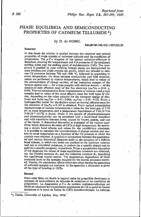
Systematically the dependence of the number of charge carriers on the cadmium(or tellurium) pressure, under which the samples with various dopes were reheat-ed at a definite temperature, was studied. The results of these measurements arerepresented in figs 15, 16, 17, 18, 19 and 20. The' figures give the concentrationof electrons and holes as a function of the cadmium pressure under which thesamples were reheated at various temperatures.Figure 15 gives the situation for the purest CdTe we could obtain (which, as
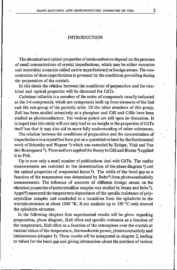
will be shown later, still contained 2.1016 Cu). It can be seen that at a definitecadmium pressure the samples change from P: to n-type.Indium-doped samples (figs 16, 17, 18) do not show p-type conductivity at
all. In the range of low cadmium pressures the crystals have a high specificresistance (106-107 [!cm). Samples prepared at higher cadmium pressures show
PHASE EQUILIBRIA AND" SEMICONDUCTING PROPERTIES OF CdTe 25
17Cd Te_1.6· 10'6Cu V .~ ::1~:",
70doe'V y. ®( ./.® -
800°· 900° 10000C, I "~ \
~ ®) \@\® ,
lognorlogp
I 16
15
o T 94546
-log PCd(afm)
Fig. IS. Theconcentration of charge carriers of CdTe-I·6.1016 Cu as a function of Tand PCd.
-2 -1
log"
Cd Te_T.3 ·10'7In.~ -
7'~ I
V VI
7000e 1/ 800° / '9000è
I I ~
'I
e '" B (!J " "i i i i i i i
17
16
15
-3 . -2 -1 0- log PCd (afml
94547
Fig.I6. The concentration of charge carriers of CdTe-l·3.I017 In as a function of Tand PCd.
The points indicated by i denote samples with a very high specific resistance.
n-type conduction. Going to higher cadmium pressures the number offree elec-trons first nearly satisfies the relation d log n/d log PCd = l. At a definite PCd'
however, the number of free electrons becomes independent of the cadmiumpressure and equal to the concentration of indium. This region is called the regionofcontrolledconductivity. CdTewith the highestindium dopeC[In]= 5.1017 cm=")shows a marked influence of the velocity of quenching to room temperatureof the samples after reheating at high temperature. The dotted line in fig. 18shows the result of slow quenching, the full drawn line the result of rapid quench-ing. This phenomenon, which is ascribed to clustering effects, will be treated insection 3.7.

26 D. de NOBEL,
17Cd Te_2 • 10'7In .A-. ;v / ~~
r: V V J
700°C I1 8000C I 900°C
OG e '" àAii i i' i i
logn
t 16
15
3 2 1 0- log PCd(atm) 94548
Fig. 17. The concentration of charge carriers of CdTe - 2.1017 In as a function of T andpCd'The points indicated by i denote samples with a very high specific resistance.
18
Cd Te-S'1O'71n P"-"'-~-"" »>/7OOV' / V V~OC./ _.I
'~~7 ".f/ yf9000C~,' P
", 0 ,"". I t,
r· I I
~I,, ,
000 0 0 " a " v .,iii i i i i i i i
16
15-4 -3 -2 -1 0
--_ log PCd (atm) 94549
Fig. 18. The concentration of charge carriers of CdTe - 5.1017 In as a function of T andpcd'The points indicated by idenote samples with a very high specific resistance. The drawn linesgive the situation after very rapid quenching of the samples from high temperature to roomtemperature, the dotted lines after less rapid quenching.
Gold-doped samples prepared at low values of PCd show p-type conduction.At a certain value O{PCd the conductivity suddenly changes to n-type. Samplescontaining 5.1016 Au cm-3 show a range in which the concentration-of holes isindependent ofPCd, i.e. a range of controlled conductivity similarto thatobservedwith n-type CdTe - In (fig. 19). Only part of this range can be covered experi-mentally due to the fact that it is situated in the vicinity ofPmln' which fact causessublimation of the samples (see 1.3). In samples containing 'gold in a higher

PHASE EQUILIBRIA AND SEMICONDUCI1NG PROPERTIES OF CdTe 27
lognor
logp
I 15
C~ Te_5 ~ 1016Ay ./"V j
SUbli~ation-, l/ 900;;_@ IregIon', 11~___ _.L.<, r ,L_ I® -, I,\ 1000"C
~, lîn 1''-/(~1<, @Î' ®
~ 700°C
\
16
14
-] -2 -1 0-log PCd (atm) 94550
Fig. 19. Theconcentration of charge carriers in CdTe-5.1016 Au samples as a function of TandPCd'
lognorlogp
Cd Te_5 ·10'7Cu V/100®y'1?/
'950oC c----!/@t
~ IV::J'
~\
~ ~:~.; !! \,/'e""" ,," :/ !! \900oC...,,'@ !! \
,~~oc'j I
IIIt- 'l-~ I
17
15
14
13-1 o 1
-log PCd(alm) Q4551
Fig. 20. The concentration of charge carriers in CdTe-5.1017 Cu samples as a furÎctionofTaildpCd'
concentration, viz. 4.1017 cm-a, a range of controlled conductivity can notbe found, The crystals show non-reproducible behaviour in the ft-typeregion, which is ascribed to cluster effects of the gold centres(see3.7). Onlythecadmium pressure at which the conductivity ofthe samples changes 'of sign can

28 D. de NOBEL
5Cd ïe: 1.5·1O'5Cu(J)reheated at 900°C, PCd- 0.41.atm
(ID .. .. aGOoc. .. 0.11 ..® .. .. 900°C. .. 0.59 ."s .. .. l000oC. .. 3.55
'. 700oe, .. 0.29 ..CdTe_1.3·1O'7In® .. sore, .. 00 ..Cd!e_20.1017In <2J '. " aoooe, , .. 0.05 ..
~I 1"CD 1--- i I ! I
I I-(2) ~@ f-<>" j,m ~® I-""' i I<2J
/ogRH(cm3Cou/-I)
I 4.
3
2
2 5 8 la_103r-1 12
Fig. 21. Temperature dependence of RH of various n-type samples.
Cd Te_2'10'7 Cu(J)reheated at 900°C PCd'" 0.85 atm@ .. .. 900°C .. 1.40 ..
CdTe_5·10'5~u® .. .. 800°C .. 1.45 ..-I)
--"_
1-- -tv
,~
'~
8
2
2 5 . la 12--'-103r' 94553
8
Fig. 22. Temperature dependence of RH of various n-type samples.
be reproduced. For 700 oe this occurred atpcd =0·4 atm; for 800 oe at PCd =1·3 atm and for 900 oe at PCd = 3·2 atm.Experiments with copper, silver and antimony dopes show the same features
as samples highly doped with gold in the p-type region (see fig. 20). Introduetionof the alkali metals offers large difficulties because of the evaporation of thedope from CdTe during the prolonged heating at high temperatures.

PHASE EQUlLffiRIA AND SEMICONDUCTING PROPERTIES OF CdTe 29
7CdTe_2"016CU (j)rehealedat 700oC,PCd"0.00245 atm /' V'r-- (6) .. .. 900°C .. 0.39atm ft
(J) .. .. 900°C .. 1.32" /' V@ .. .. 800°C .. 0.05~" / ./
/'_;~/ /'-1)
~.~~;V ~ '/
i /' ~V
/ /-
/-/ 9'~
Ar
6log RH
(cm3Coul
Î 5
3 8
Fig. 23. Temperature dependence of RH of various p-type samples.
q4554
9r-----~----~------r-----~----_.----_.
8~----+7~~-+~--~-log RH
(anr;'I-)--I-~-I--<;)I!"__--1----t----t-----t---t
Cd Te _ 1018Ag (j)reheated at 950°C PCd- 4.47afm6 1---1+--/'-1-- @.. 9800C .. 6.30"
CdTe_5·10''lCu @ .. 800°C" 1.26"
@ .. 800eC .. 1.12"
53~----4~----~5~--~6~----~7----~8~--~/9---_103r'
Fig. 24. Temperature dependence of RH of various p-type samples.
As will be seen in chapter 3 of this study much information can be drawnfrom log 'n (or p) ys 10gPcd diagrams.In order to obtain information about the ionization energy of the centres
responsible for the n- or p-type conductivity the Hall effect of a: large numberof samples with various dopes was measured as a function of the temperature.The results are represented in figs 21, 22, 23, 24 and 25; these results are inter-preted in section 2.2.
94555

30 D. de NOBEL
3
Cd Te_5· 10'7Inreheated at 800°CPedo 8.0· 10-3atfn I
I, [r /, I /
/ /1/ V.:'"
RH
/ // I
.~
/"f /
i ...
7
6
log e(nem)
log RH '(em3Courl)
l'J 2 5
01.4. 1.8 2.2 2S 3_ 103 T-1 .•• '"
Fig. 25. Temperature dependence of RH and ~ of an n-type CdTe - 5.1017 In sample.
2
CdTe_2.10'5Cu (J) reheated at 9ÓOoC,PCd z 0.44 atm@ .. " 800°C. " 0.11 _"Q) " " 900°C, " 0.59 "@ " "1000oC. " 3.55 "® " " 700°C, " 0.29 "--TI-<---~.
g) -i---<'- .JiI.-e. Q)
__.y-- ~-;(lJll
®
log I'(.nem)
f
o
-1o 2 694557
8 10--"'1037"'
12
Fig. 26. Temperature dependence of e of various n-type samples.
1.6.4. Measurement of the resistance'
The resistance r was determined by measuring the voltage drop over twoprobes by a compensation method when a direct current was passed through the

, ,
PHASE EQUILmRIA AND SEMICONDUCTING PROPERTIES OF CdTe 31
crystal. By reversing the current thè homogeneity of the crystal was checked.From these measurements the specific resistance e was obtained by means ofthe relation e = rbdjl, in which I = distance between the probes, b =width andd = thickness of the sample. The results of somemeasurements of the resistanceof crystals prepared under various' conditions are shown as a function of the-temperature in figs 26, 27 and 28.
BCd Te_2·1016Cu. (j) reheatedal 700°C,
Pcd=2.45· /O~3alm@ reheated al 900 °C,
PCd = 0.39 alm
I/:Vl,0V;
~,/
/'.>I
7
6log I'
(.J2cm) 5
Î 4
J
2
5 6 7 8- 103 r-I 94558
Fig. 27. Temperature dependence of (}of various p-type samples.
3.4 3.6 3.8 4.0 5.0- 103T-1 94559
Fig. 28. Temperature dependence of (}of various p-type samples.
---------------~-,'-, _, - -",-- - - "
Cd Te_5'1016Au, reheated al 900°C(j) Pru - 0.11 atm~ PCd = 0.22 alm® Pru = 0.40alm
5
/)' '_/
/ /' T11/ //. /
@~ " /'/ -, " . '
I---Q5
logp(.!lcm)
7
12
6
5
2
5
32 D. d~ NOBEL
By combining the data for resistance and Hall-effect measurements, themobili-ty ofthe charge carrierscould be obtained. Forthe case of charge carriers ofonetype only, which applies to CdTe in the temperature range in which our measure-ments were made, the following relation holds:
p, = RH e-1r+in which p, = mobility in cm2/Y sec, RH = Hall coefficient in cm3/coulomb,e = specific resistance" in [!cm, and f = 3n/8. The mobility of n- and p-typesamples will be discussed in section 2.3.
1.6.5. Measurement of the dielectric constant
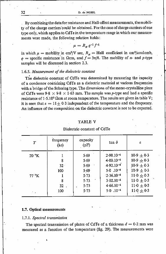
The dielectric constant of CdTe was determined by measuring the capacityof a condensor containing CdTe as a dielectric material at various frequencieswith a 'bridge of the Schering type. The dimensions of the mono-crystalline pieceof CdTe were 9·8 X 9·8 X 1·63 mm. The sample was p-type and had a specificresistance of 1.5.103 [!cm at room temperature. The results are given in table Y;it is seen that 8 = 11± 0·3 independent of the temperature and the frequency.An influence of the composition on the dielectric constant is not to be expected.
TABLE Y
Dielectric constant of CdTe
Tfrequency capacity tan {J
I8
(kc) (PF)
20 oK 1 5·69 2·98.10-4 10·9 ± 0·38 5·69 4.00.10-4 10·9 ± 0·3
32 5·69 4·92.10-4' ,10·9 ± 0·3100 5·69 5.0 .10-4 10·9 ± 0·3
77 oK 1 5·73 '2·36.10-4 n-o ± 0·38 5·73 3.02.10-4 11·0 ± 0·3
32 . 5·73 4.66.10-4 11·0 ± 0·3100 5·73 5.0 .10-4 11.q ± 0·3
1.7. Optical measurements
1.7.1. Spectral transmission
The spectral transmission of plates of CdTe of a thickness d = 0·2 mm wasmeasured as a.function of the temperature (fig. 29). The measurements were

PHASE EQUILIBRIA AND SEMICONDUCTING PROPERTIES OF CdTe 33
Fig. 29. The transmission of CdTe as a function of the wavelength at various temperatures.The dotted line gives the transmission at 293 "K after cooling down from the highest tempera-tures of measurement.
performed up to 983 "K. Higher temperatures could not be employed becauseof the decomposition of CdTe. After measuring the transmission at 983 "K theroom temperature measurement was repeated, which did not differ much fromthe first measurement (dotted curve in fig. 29). This indicated that no irreversiblechanges had occurred.
1.7.2. Electromotive force produced by irradiation of a crre p-n junction (photo-emf.)
A photo-emf. cell was made starting with a plate of monocrystalline n-typeCdTe. One side of the plate was covered by an AuCl3 solution, which after someminutes produced a p-type surface layer covered by gold. After removing thesolution, contacts were made to both the bulk material and the p-type layer,after which the cell could be used (fig. 30).
" 111
945b1
D
Fig. 30. A CdTe photo-emf. cell, consisting of a piece of n-type CdTe Cc), having a p-type, region CB) covered with a gold screen CA). Contact to the n-type region is made by an alloyedindium contact CD).
The spectral distribution of the photo-emf, of this cell shows a sharp limit atthe long-wavelength side (fig. 31). The position of this limit was determined attemperatures between 77 and 480 "K (see fig. 32).
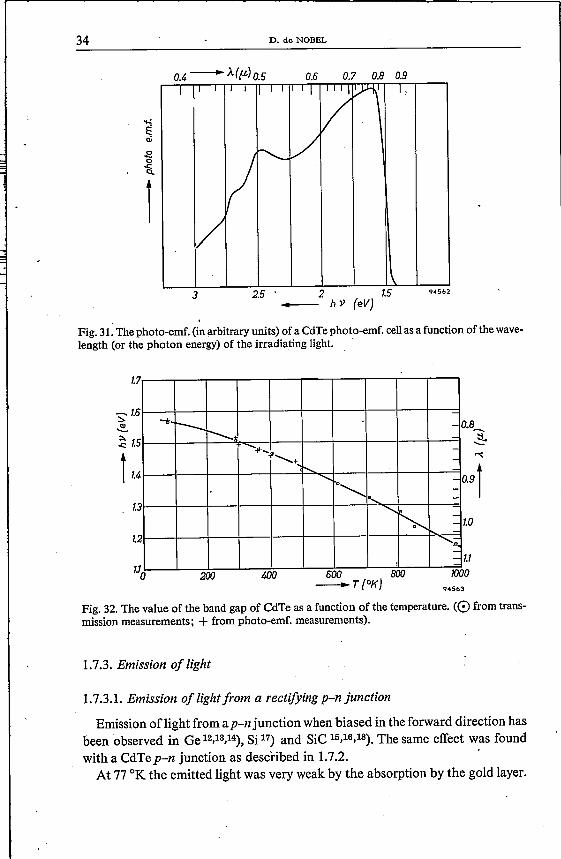
34 D. de NOBEL
...,Éa)
1
2.5 . 2 T.5_ h)/ (eV)3 945b2
Fig. 31. The photo-emf. (inarbitrary units) of a CdTe photo-emf. cell as a function ofthe wave-length (or the photon energy) of the irradiating light. .
T.7
-=-t :-- -
~j -~"'.j> -
.........+ -........
........................
--I·<, -
<,r-, ---
.........~!
-
îT.6
~~ T.5
t T.4
1.3
1.2
200
0.8~"(
T.O
T.T1000
94563
Fig. 32. The value of the band gap of CdTe as a function of the temperature. (0 from trans-mission measurements; + from photo-emf. measurements).
1.7.3. Emission of light
1.7.3.1. Emission of lightfrom a rectifying p-n junction
Emission oflight from a p-n junction when biased in the forward direction hasbeen observed in Ge 12,13,14), Si 17) and SiC 15,16,18). The same effect was foundwith a CdTe p-n junction as described in 1.7.2.
At 77 "K the emitted light was very weak by the absorption by the gold layer.

PHASE EQUILIBRIA AND SEMICONDUCTING PROPERTIES OF CdTe 35
For this reason the gold layer was removed by boiling the crystal in a 10% KCNsolution, after which a very thin iridium layer or a gold screen was evaporatedonto the p-type region.
The spectral distribution could be determined only roughly, because a mono-chroma tor with a wide slit (2 mm) had to be used. The result is shown in fig. 33.
-À (ft)
0.9 . 1.0
F'è.l00::;,
'f!~-c:IIIc:8 IIIÏ I'§ Ira I
a~--~~----~'-'~-=-~--~~a1.6 1.5 1.4 1.3 1.2
hV(eVJ_945b4
Fig. 33. The emission of a CdTe p-n junction biased in the forward direction. The absorptionconstant is given by a dashed line.
1.7.3.2. Photoluminescence
The photoluminescence was studied at 77 ok with crystals prepared undervarious conditions. The crystals were irradiated by light from a lOOO-Wsuperhigh-pressure mercury lamp. The infra-red radiation was cut off by a saturated .CuS04 solution. The radiation was measured by a recording quartz mono-chromator with a light chopper and an infra-red sensitive photomultiplier. Thespectral distributión of the luminescence of CdTe - 5.1017 In crystals at 77 "Kis shown in fig. 34. The crystals were prepared at 900 °C under a cadmium pres-sure of'O-I atm and 0·01 atm. The crystals prepared under 0·1 atm cadmium pres-sure showed a large peak at 1-42 eV and a small peak at 1·10 eV. The crystalsprepared under 0·01 atm cadmium pressure showed the same large peak at1·42 eV but a smaller peak at 1·06 eV. The spectral distribution ofthe luminescen-ce of CdTe - 5.1016 Au, reheated at 900 °C under a cadmium pressure ofO·2 atm,is shown in fig. 35.

36100
~ 80~c::;,~ 60..!?.0"iiic: 40~.!:
1 20
D. de NOBEL
fA\f \, ,\,1\\,, \\ 1\a 'b,
I \\ \\ ..._ ....bI .... x/GO, '",- ,
1/1 \~ ....~
/ , --v- ....
~~/ I'Z- r!!!-- ....
0,.6 1.4 1.2 1.0 0.8eV ... -- 94565
Fig. 34. The luminescence spectrum of CdTe- 5.1017 In at 77 OK.
(a) CdTe-5.1017 In, reheated at 900 "C, PCd = 0'1 atm;(b) CdTe- 5.1017 In, reheated at 900°C, PCd = 0'01 atm.
100
80~c::;,.,,; 605..._.0'iii 40~.!:;
120
0
,1',~\I \
, ! \1 \\I,,f l-/a ' \r b, \, \
IJ 1\\.t-V '\.:' .....
1.6 1.4 1.2 1.0eV .... --
Fig. 35. The luminescence spectrum of CdTe-S.1016 Au at 77 OK.
(a) CdTe-S.1016 Au, reheated at 900 °C, PCd = 0'1 atm, immediately after preparation;(b) CdTe- 5.1016 Au, reheated at 900 °C, PCd = 0'1 atm, after heating at 100 °C for 1 hr (on
an enlarged scale to bring the intensity of the highest peak at 100).
Immediately after preparation of the sample the luminescence spectrum showstwo bands, one at about 1·40 eV and another at 1·27 eV. After reheating thesample during one hour at 100 °C and cooling to room temperature the peaksremain at the same place; however the peak at 1·27eV has decreased in inten-sity (see fig. 35).With CdTe doped with Ag or Cu only a peak at about 1·40 eV was found,

- -------~--- ~ ~-~-~-------~-------------------
PHASE EQUILIBRIA AND SEMICONDUCTING PROPERTIES OF CdTe
independent of the conditions of preparation. A very broad band in the lumines-cence spectrum of CdTe peaking at 0·54 eV is mentioned by Brown 28). Wecould not find any indications of such a band.
100
;f 80c::. ::;,
.cl 60....
.E:..20
~ 40
1 20
........\............ \
_~ ............b
\ a\
\\\ \\
\\\x 10
./\ \
\' '---- --_a2.0 945671.5 1.0
eV__--
Fig. 36. The photoconductivity spectrum of CdTe-5.1017 In at room temperature.(a) CdTe- 5.1017 In, reheated at 900 DC,PCd = 0·01 atm;(b) CdTe- 5.1017 In, reheated at 900 DC,PCd = 0·1 atm .
100
80
F'e: 60::;,
-e..!2...2 400-e.~
I 20
a
." '\\.."..............
-- b \\a \~
q\
) \\
[2.0 1.0 945681.5
eV-Fig. 37. The photoconductivity spectrum of CdTe-5.1016 Au at room temperature.(a) CdTe-5.1016 Au,reheated at 900 DC,PCd = 0·1 atm,immediately after preparation;(b) CdTe-5.1016 Au, reheated at 900 DC,PCd = 0·1 atm, after heating at 100 DCfor 1 hr (on
an enlarged scale to bring the maximum at 100).
1.7.4. Photoconductivity
The measurement of the photoconductivity as a function of the wavelengthof the exciting light showed one peak at ~ 1·49eVwhich was rather independent
37
38 D. de NOBEL
of the way in which the samples were prepared; in addition other peaks appearedwhich were characteristic ofthe examined sample.
For·CdTe-5.1017Inpreparedat900°Cunderpcd =0·1atmandpcd= 0·01 atmthe spectrum is shown in fig. 36. CdTe - 5.1017In (900 °C, ]lCd = 0·1 atm)showed a peak at 1·46eV and a very weak one at 1·07 eV. For CdTe - 5.1017In(900 °C, PCd = 0·01 atm) the peak at 1·46 eV showed to be very large, but nopeak at 1·07 eV was found.
In very pure samples a peak was found at 1·49 eV.CdTe-5.1016 Au (900°C, PCd = 0·2 atm) showed a verylarge peak at 1·40eV.
Heating at 100 °C markedly decreased the intensity of this peak (fig. 37).Samples CdTe-Ag and CdTe-Cu only showed a peak at 1·49eV.
1.7.5. Measurement ofthe refractive index
The refractive index n was determined by a method described by Oswald andSchade 19). A planparallel optically polished plate of CdTe of thickness d wasused for this experiment. The reflection index R and the absorption coefficient Kcan be determined from the intensity of the reflected light (ir) and the transmittedlight (it) at various wavelengths in the infra-red region. Between these quantitiesthe following relations exist:
i,= ioR { 1 + (1 - R)2 } ,e2Kd _ R2
. . (1 - R)2e-Kdt = t ,tOl _ R2e-2Kd
in which io is the intensity of the light falling on the sample. The value of iocan be determined by measuring the reflection after plating the CdTe slide withsilver.
From the measured values ofir, it and io the values ofK and R can be calculated.Then it is possible to calculate n by the relation
n = (1+ R)/(l - R) ± [{(1 + R)/(l - R)}2 -1 - KJ..f4n]'/a.
If KJ..f4n is small this formula simplifies to
n = (1 + R'/')/(l - R'll).
As the transmission in the studied infra-red region showed to be very large, theKJ..f4n term could be neglected and the simplified formula could be used. Infig. 38 the reflection coefficient R = ir/io and the refractive index n are shown

PHASE EQUILIBRIA AND SEMICONDUCTING PROPERTIES OF CaTe 399
7 8 9-À ((-t)
105 6
Fig.38. The reflection coefficient R (in per cent) and the refractive index 11 as a'function ofthe wavelength (in microns).
as a function ofthe wavelength. The plates were too thick to carry out measure-ments at wavelengths smaller than 5 fJ., the absorption in this region becomingtoo large. The value of n in the wavelength region in which it is constant is2·75 ± 0·01.
(To be continued.)
. .