photonic-integrated circuits with non-planar topologies
TRANSCRIPT

Photonic-integrated circuits with non-planartopologies realized by 3D-printed waveguideoverpassesALEKSANDAR NESIC,1,6 MATTHIAS BLAICHER,1,2 TOBIASHOOSE,1,2 ANDREAS HOFMANN,3 MATTHIAS LAUERMANN,1,4
YASAR KUTUVANTAVIDA,1,2 MARTIN NÖLLENBURG,5 SEBASTIANRANDEL,1 WOLFGANG FREUDE,1 AND CHRISTIAN KOOS1,2,4,*
1Karlsruhe Institute of Technology (KIT), Institute of Photonics and Quantum Electronics (IPQ),Engesserstrasse 5, 76131 Karlsruhe, Germany2Karlsruhe Institute of Technology (KIT), Institute of Microstructure Technology (IMT),Hermann-von-Helmholtz-Platz 1, 76344 Eggenstein-Leopoldshafen, Germany3Karlsruhe Institute of Technology (KIT), Institute for Automation and Applied Informatics (IAI),Hermann-von-Helmholtz-Platz 1, 76344 Eggenstein-Leopoldshafen, Germany4Vanguard Photonics GmbH, Gablonzer Strasse 10, 76185 Karlsruhe, Germany5TU Wien, Institute of Logic and Computation, Algorithms and Complexity Group, Favoritenstrasse 9-11,1040 Vienna, [email protected]*[email protected]
Abstract: Complex photonic-integrated circuits (PIC) may have strongly non-planar topologiesthat require waveguide crossings (WGX) when realized in single-layer integration platforms. Thenumber of WGX increases rapidly with the complexity of the circuit, in particular when it comesto highly interconnected optical switch topologies. Here, we present a concept for WGX-free PICthat relies on 3D-printed freeform waveguide overpasses (WOP). We experimentally demonstratethe viability of our approach using the example of a 4 × 4 switch-and-select (SAS) circuitrealized on the silicon photonic platform. We further present a comprehensive graph-theoreticalanalysis of different n × n SAS circuit topologies. We find that for increasing port counts n ofthe SAS circuit, the number of WGX increases with n4, whereas the number of WOP increasesonly in proportion to n2.
© 2019 Optical Society of America under the terms of the OSA Open Access Publishing Agreement
1. Introduction
Photonic integrated circuits (PIC) are becoming increasingly complex, incorporating thousands ofphotonic devices on a single chip [1,2]. The silicon photonic (SiP) platform, in particular, standsout to high integration density and offers high-yield fabrication on large-area substrates usingmature CMOS processes [3,4]. However, as the complexity of PIC increases, non-planar circuittopologies with hundreds or even thousands of waveguide crossings (WGX) are unavoidable,and the number of WGX often increases in a strongly nonlinear way with the complexity of thecircuit. As a consequence, compact WGX have evolved into key building blocks, and substantialresearch effort has been dedicated to optimizing their performance. This has led to remarkably lowinsertion loss (IL) of 0.017 dB and crosstalk as small as –55 dB at λ = 1550 nm, demonstrated forpartially etched multi-mode interference (MMI) structures that feature a relatively large footprintof approximately 30 × 30 µm2 [2]. Fully etched MMI structures allow to reduce the footprint to,e.g., 9 × 9 µm2, but losses and crosstalk increase to, e.g., 0.028 dB and –37 dB, respectively [5].Arrays of WGX can be compactly realized by exploiting Bloch modes in multi-mode waveguides:For SiP structures fabricated by electron-beam lithography, values of IL = 0.019 dB and crosstalk
#357874 https://doi.org/10.1364/OE.27.017402Journal © 2019 Received 16 Jan 2019; revised 15 Mar 2019; accepted 5 Apr 2019; published 7 Jun 2019
Vol. 27, No. 12 | 10 Jun 2019 | OPTICS EXPRESS 17402

of less than –40 dB per WGX were demonstrated for a 101 × 101 WGX array with a 3 µmwaveguide pitch [6]. For optical lithography, the best reported values for Bloch mode WGXare IL = 0.04 dB and crosstalk less than –35 dB for a 1 × 10 array of crossings with a 3.25 µmwaveguide pitch [7].
However, while these demonstrations are impressive, even IL of the order of a few hundredthsof dB and crosstalk of the order of –40 dB per WGX may have a substantial impact on theperformance of large-scale PIC that may comprise tens of thousands of crossings. A primeexample in this context are high-radix switches that rely on the so-called switch-and-select (SAS)architecture [8]. The SAS scheme offers low crosstalk and simple control but requires a complexand highly non-planar interconnect network that provides a dedicated waveguide from each inputto each output port. In fact, finding a layout that gives the minimum number ηn,n of WGX in ann × n SAS circuit, and generally in any circuit, is an NP-complete problem [9], and ηn,n scaleswith n4/16 according to a still unproven conjecture [10,11]. This leads to tens of thousands ofWGX for n = 32 and to approximately one million WGX for n = 64. To illustrate the associatedperformance penalty by WGX crosstalk, let us consider an example of a waveguide that crossesan array of 100 other waveguides with a crosstalk of –40 dB in each of the crossings. Assumingincoherent superposition of the various crosstalk contributions and interpreting them as randomnoise that deteriorates the signal, the signal-to-noise power ratio (SNR) would amount to 20 dB.For a 32QAM signals, this would lead to a bit-error ratio (BER) of 6 × 10⁻⁴ [12], which is onlyslightly below the 4.5 × 10⁻³ limit for hard-decision forward-error correction (HD-FEC) with7% overhead [13]. This represents a significant deterioration of the signal quality. For 64QAM,which is envisaged for high-speed transmission systems with data rates beyond 500 Gbit/s perwavelength, an SNR of 20 dB would even be insufficient to reach the HD-FEC limit. Suchcrosstalk levels hence represent a significant deterioration of the signal quality. The situationmay become even worse in case the crosstalk signals are superimposed coherently. Moreover, afew hundredths dB of IL per WGX would result in several dB of overall IL that is accumulatedover the 100 crossings. This example illustrates that large-scale PIC with highly non-planartopologies may face performance limitations when realized by WGX in single-layer integrationplatforms.
To overcome the limitations of conventional WGX, multi-layer PIC have been proposedexploiting multiple stacked waveguide layers, realized from silicon [14,15], silicon nitride(Si3N4) [16,17] or as a combination of both waveguide technologies [18–23]. The deposition ofthe upper layers is typically done by chemical vapor deposition (CVD) and involves chemical-mechanical planarization (CMP) of intermediate SiO2 cladding layers that separate the waveguidelayers. While simple two-layer implementations offer decent performance [20,22], three-layerstructures have been shown to greatly reduce inter-layer crosstalk while maintaining efficientinterlayer coupling [15,21,23]. This allows to reduce the crosstalk to less than –56 dB withremarkably low interlayer coupling losses of less than 0.15 dB from the bottom to the top layerusing a pair of vertical directional couplers of approximately 190 µm length per side [21,23].However, while this approach offers utmost scalability and the ability to cross entire groups ofwaveguides, the integration of silicon or silicon nitride waveguides into back-end metal layerstacks introduces additional technological complexity and is not yet established as part of thetechnology portfolios offered by silicon photonic foundries. In addition, all multi-layer PICdemonstrations so far are limited to silicon photonics.
In this paper we demonstrate hybrid 2D/3D photonic integration based on direct-write laserlithography as an alternative approach for realizing non-planar circuit topologies. Our approachis based on 3D-printed freeform polymer structures [24], which we refer to as optical waveguideoverpasses (WOP). WOP are realized in situ by two-photon polymerization [25], which haspreviously been used for fabrication of so-called photonic wire bonds that enable low-losssingle-mode connections across chip boundaries [26–29]. The devices offer low crosstalk of less
Vol. 27, No. 12 | 10 Jun 2019 | OPTICS EXPRESS 17403
than –75 dB and allow to bridge series of parallel waveguides, thereby replacing a multitude ofWGX. We demonstrate the viability of our approach by realizing a 4 × 4 SAS circuit. Based ona graph-theoretical analysis, we estimate that the number of WOP needed to realize a WGX-freen × n SAS PIC scales in proportion to n2/2. A 64 × 64 SAS circuit would hence requireonly approximately 2000 WOP as opposed to the estimated one million conventional WGX.Fabrication of WOP may be efficiently combined with 3D-printing for die-level packaging[26–29], and offers the opportunity to locally incorporate multi-layer elements into standard SiPcircuits, fabricated through readily available foundry services. The concept of 3D-printed WOPis not limited only to silicon photonics but may be transferred to a wide range of alternativephotonic integration platforms.
The paper is structured as follows: In Section 2 we introduce the concept of 3D-printedWOP. A graph-theoretical analysis of the number of necessary WOP and WGX for realizingsurface-coupled n × n SAS devices is provided in Section 3. Design and experimental testing ofthe demonstrator device are explained in Section 4. Appendix A provides definitions of graphtheory terms. Appendix B gives further details of the graph-theoretical approach used for theanalysis in Section 3. Appendix C gives a detailed graph-theoretical analysis of the number ofnecessary WOP and WGX for realizing facet-coupled SAS devices.
2. Concept of waveguide overpasses (WOP)
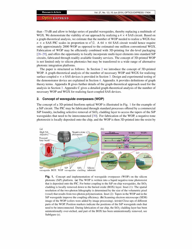
The concept of a 3D-printed freeform optical WOP is illustrated in Fig. 1 for the example ofa SiP circuit. The PIC may be fabricated through standard processes offered by a commercialSiP foundry, including selective removal of SiO2 cladding layer to access the tapers of the SiPwaveguides that need to be interconnected [30]. For fabrication of the WOP, a negative-tonephotoresist is locally deposited onto the chip, and the WOP is then 3D-printed into the resist by
Fig. 1. Concept and implementation of waveguide overpasses (WOP) on the siliconphotonic (SiP) platform. (a) The WOP is written into a liquid negative-tone photoresistthat is deposited onto the PIC. For better coupling to the SiP on-chip waveguides, the SiO2cladding is locally removed down to the buried oxide (BOX) layer. Inset (1): The spatialresolution of the two-photon lithography is determined by the size of the volumetric pixel(voxel) that results from two-photon polymerization. Inset (2): Tapers in the WOP and in theSiP waveguide improve the coupling efficiency. (b) Scanning electron microscope (SEM)image of the WOP (colors were added by image processing). (c)-(e) Close-ups of differentparts of the WOP. Position markers indicate the positions of the SiP waveguide ends thatneed to be interconnected. During fabrication of our chip, the SiO2 cladding layer has beenunintentionally over-etched, and part of the BOX has been unintentionally removed, seeSubfigure (e).
Vol. 27, No. 12 | 10 Jun 2019 | OPTICS EXPRESS 17404

direct laser writing based on two-photon polymerization. After exposure, the resist is removed,and the free-standing WOP structures are clad by a low-index polymer that acts as cladding andhumidity protection (not shown in Fig. 1). Depending on the length, WOP may bridge tensor even hundreds of planar waveguides in the SiP device layer. Figure 1(b) displays scanningelectron microscope (SEM) images of the two WOP on our demonstrator device before thecladding was applied, with colors added by image processing for better visualization. Figures1(c)–1(e) show close-ups of different parts of the lower WOP and demonstrate the accuracyof the direct laser writing method. The two-photon lithography system uses CMOS patternedsilicon markers for automated detection of the SiP waveguides that need to be interconnected.The 3D-printing time of one WOP is about 30 s with a significant potential for further reduction.The refractive index of the WOP core material amounts to nWOP ≈ 1.53, and the cladding hasa refractive index of ncladding ≈ 1.36 at 1550 nm. Note that the concept has been illustrated forthe SiP platform here but can generally be applied to a wide range of PIC technologies. As anexample, 3D-printed photonic wire bonds can be efficiently coupled to surface-coupled [28] andedge-coupled InP-waveguides [29].
3. Theoretical analysis of non-planar switch-and-select (SAS) circuit topologies
To experimentally demonstrate the viability of our approach, we use an m × n SAS circuit asan example of a PIC requiring many WGX. In the m × n SAS architecture, each of the m inputports feeds a 1 × n switch distributing the light to one of the n output ports, and each of the noutput ports is fed by an m × 1 switch, which selects light from one of the m input ports. Anillustration of a basic non-optimized implementation of a 4 × 4 SAS architecture is shown inFig. 2(a), featuring a total number of 36 WGX in the depicted case, which would scale up to atotal number of
η(basic)n,n =
(n(n − 1)
2
)2
(1)
for the case of an n × n SAS circuit. In the following, we show that these circuits can be realizedwith a significantly smaller number of WOP than the number of WGX, even if the layout ofthe circuit is optimized to reduce the number of WGX. To this end, we exploit graph theory toinvestigate the scaling of WGX and WOP number for increasing port counts n. For the remainderof this section, we consider the case where input and output ports are accessible from the topsurface of the PIC and can hence be positioned anywhere on the chip. This case is referred to assurface coupling. Surface-coupled PIC may, e.g., rely on grating couplers, SiP waveguides thatare bent upwards by ion implantation [31], or on 3D-printed lensed couplers [32]. We only givea summary of the results here; mathematical details can be found in Appendix B. In Appendix C,we also discuss the case of facet coupling, for which light is coupled to and from the PIC viawaveguide facets along the chip boundary.
As a first step of the layout optimization, we exploit the fact that surface coupling allows toroute waveguides around the couplers. This is illustrated in Fig. 2(b) for the example of a 4 × 4SAS. In this implementation, we consider the 1 × n and m × 1 switches at the input and outputports as discrete entities that cannot be subdivided and that may hence be considered as lumpedelements (LE). This leads to representation of the SAS circuit by a complete bipartite graphKm,n having two sets M and N of m and n vertices, respectively. Each vertex of set M representsan input port of the SAS and its corresponding 1 × n switch, and each vertex of set N representsan output port and the associated m × 1 switch. Each vertex of one set is connected to eachvertex of the other set by a total of mn edges that represent optical waveguides. In the following,we restrict our consideration to the particularly relevant cases of Kn,n, for which the number mof input ports equals the number n of output ports. A generalization to the case of Km,n can befound in Appendix B.
Vol. 27, No. 12 | 10 Jun 2019 | OPTICS EXPRESS 17405

Fig. 2. Comparison of layouts of a 4 × 4 optical switch-and-select (SAS) circuit for surfacecoupling. (a) Basic layout for single-layer waveguide technology without any optimizationfor reduced numbers of waveguide crossings (WGX). (b) Optimal layout for single-layerwaveguide technology, minimizing the number of WGX by routing of waveguides aroundthe coupling elements. The formula for η(surf)
n,n is a conjecture for the minimum possiblenumber of WGX for an n × n SAS, if the 1 × n and n × 1 switches at the input and outputports are lumped elements (LE) [10,11]. For large port counts n, the number of WGX isconjectured to scale with n4/16. (c) Best found, but not necessarily optimal layout for asingle-layer 4 × 4 SAS circuit, in which the 1 × 4 and 4 × 1 switches have been realized asbinary trees (BT) of 1 × 2 and 2 × 1 switches. A general analysis of this circuit topologyfor arbitrary n is subject to ongoing investigations. (d) Best found, but not necessarilyoptimal WGX-free layout for hybrid 2D/3D circuits, minimizing the number of WOP. Theswitches are realized as BT in the same way as in (c). The formula for µ(surf, BT)
n,n is an upperbound for the minimum number of WOP. The optical paths that were used for the crosstalkmeasurement in Section 4 are marked in green (Path 1) and in blue (Path 2). The arrowsindicate the direction of light propagation for the crosstalk measurement. The drive currentof MZI1 is modulated by a sinusoidal signal for highly sensitive lock-in detection of theweak crosstalk signals.
Vol. 27, No. 12 | 10 Jun 2019 | OPTICS EXPRESS 17406

For conventional SAS implementations in single-layer waveguide technology, a layout withthe smallest possible number of WGX can be achieved by optimizing the drawing of thecorresponding graph model for finding the minimum number of edge crossings (or just crossings),which is an NP-complete problem [9]. Up to now [10], there is only a conjectured formula forthe minimum possible number of crossings (crossing number), based on a straightforward graphdrawing algorithm, only proven to give an upper bound [11],
η(surf)n,n =
⌊n2
⌋2⌊n − 1
2
⌋2
. (2)
In this relation, bxc denotes the floor function. For large n, the conjectured crossing numberscales with n4/16, thereby reducing the number of WGX by a factor of 4 compared to thesimplistic non-optimized waveguide routing shown in Fig. 2(a). Note that the best publishedresult for the lower bound of the crossing number in complete bipartite graphs Kn,n states thatfor large n the crossing number scales at least with 0.83·n4/16 ≈ n4/19.28 [33]. However, thisis a theoretical result for the case of large n, which has not been supported by drawings of thecorresponding graphs. In fact, for complete bipartite graphs, no drawings are known that leadto lower number of crossings than conjectured by Eq. (2). We therefore use the conjecturedformula and its corresponding drawing as a basis for our analysis of the scaling of WGX forincreasing port counts n. For an n × n SAS circuit with n = 16, this would lead to a total numberof 3136 WGX.
Regarding hybrid 2D/3D SAS circuit implementations based on WOP, we again start from thecomplete bipartite graph Kn,n and determine the number of WOP by subtracting the maximumnumber of edges that can be realized without crossings (the number of edges in the spanningmaximum planar subgraph) from the total number of edges. The total number of edges in Kn,n isn2, and 4n – 4 edges can be realized without crossings [34]. The number of missing edges henceamounts to
µ(surf)n,n = n2 − (4n − 4) = (n − 2)2 (3)
and equals the number of WOP necessary to complete the SAS circuit, assuming that each WOPcan cross an arbitrary number of planar waveguides, and that crossings of 3D WOP can beavoided, see Appendix B for more details. Note that the length of a WOP is only limited by thewrite field size of the two-photon lithography system, which currently amounts to approximately500 µm × 500 µm. In the future, these limitations may be overcome by high-precision stitchingof structures that extend across several write fields. Using Eq. (3), we calculate a total number of196 WOP for an SAS circuit with n = 16, which is considerably smaller than the correspondingnumber of WGX. A comparison of the scaling of WGX and WOP numbers for increasing portcount n is given in the second and third column of Table 1.
As a further step of the circuit layout optimization, we may split up the 1 × n and the n × 1switches at the input and the output into binary trees (BT) of 1 × 2 and 2 × 1 switches, see Fig.2(d). This allows to reduce the number of WOP to
µ(surf, BT)n,n =
⌈(n − 2)2
2
⌉, (4)
see Appendix B for an explanation. In the last relation, dxe denotes the ceiling function. Theassociated WOP numbers for increasing port counts n are indicated in the fourth column of Table1. Note that the same technique with BT switches may also be applied to the single-layer SAScircuit architecture as illustrated in Fig. 2(c). For n = 4, we could not find a layout that reducesthe number of WGX as compared to the implementation with LE switches. Note that the SAScircuit with BT switches is not any more a complete bipartite graph Kn,n – an analysis of suchcircuit topologies has recently been published in [35]. Note further that for increasing port counts
Vol. 27, No. 12 | 10 Jun 2019 | OPTICS EXPRESS 17407

Table 1. Quantitative Comparison of Surface-Coupled n × n Switch-and-Select (SAS) CircuitImplementations Based on WGX in Single-Layer Circuits and on WOP in Hybrid 2D/3D Photonic
Integrationa
Total number Maximum number along any optical path
SAS (n × n) WGX (LE) WOP (LE) WOP (BT) WGX (LE) WOP (LE & BT)
4 × 4 4 4 2 1 1
8 × 8 144 36 18 9 1
16 × 16 3136 196 98 49 1
32 × 32 57 600 900 450 225 1
64 × 64 984 064 3 844 1 922 961 1
aThe total number of WGX increases approximately in proportion to n4/16, whereas the number of WOP scales withn2 for the case of lumped-element (LE) switches, and with n2/2 in case the switches are decomposed into binary trees(BT) of 1 × 2 and 2 × 1 switches. The maximum number of WGX along any optical path increases approximately inproportion to n2/4 for the case of LE switches, whereas the maximum number of WOP along any optical path amountsto 1 in both cases of LE and BT switches.
n of the SAS circuit with LE switches, the number of WGX increases with n4/16, whereas thenumber of WOP of the SAS circuit with BT switches increases only in proportion to n2/2. Asa consequence, the number of WOP in a 16 × 16 SAS circuit with BT switches is nearly twoorders of magnitude smaller than the number of WGX with LE switches, and for a 64 × 64 SAS,the numbers differ by nearly four orders of magnitude, see Table 1.
Besides the total number of WGX or WOP in the circuit, the maximum number of suchelements along any optical path through the circuit is an important figure of merit. For thesingle-layer implementation of the SAS circuit with LE switches, the biggest number of WGXalong an optical path amounts to
ξ (surf)n,n =
(⌈n2
⌉− 1
)2, (5)
which scales with n2/4 for large n, see Appendix B for details. The corresponding numbers forincreasing port counts n are given in the fifth column of Table 1. For an SAS circuit with n = 16,this leads to up to 49 WGX along a single optical path. In contrast to that, the number of WOPcan be kept to at most one along each path, see last column of Table 1.
Note that these discussions are independent of 3D-printed structures as a specific way to realizewaveguide overpasses and that the findings can be broadly applied to other kinds of overpasses,e.g., in multilayer circuits [15,21,23]. 3D-printed WOP are particularly attractive for use cases inwhich the number of devices and/or the number of WOP per device are limited, while ultra-lowcross-talk and/or the inherent flexibility of 3D printing are important. In contrast to that, thetechnique might suffer from limited throughput when applied to very complex circuits withthousands of WOP required on a single chip. In this case, monolithically integrated multi-layercircuits [15,21,23], might offer better scalability.
4. Device design, fabrication and experimental characterization
To demonstrate the viability of the WOP concept, we realized a 4 × 4 SAS device, similar to theone illustrated in Fig. 2(d), featuring two WOP. The device was realized on a silicon-on-insulator(SOI) wafer having a 220 nm-thick device and a 2 µm-thick buried oxide layer. All waveguidesare realized as oxide-covered strip waveguides with standard width of 500 nm. The SAS circuitconsists of four 1 × 4 switches at the input and four 4 × 1 switches at the output. Each of the1 × 4 switches is realized as a BT of three 1 × 2 switches, and the same technique is applied to the4 × 1 switches. In general, for realizing a 1 × n switch as a BT, we need (n – 1) 1 × 2 switches,
Vol. 27, No. 12 | 10 Jun 2019 | OPTICS EXPRESS 17408

each of which consists of a Mach-Zehnder interferometer (MZI) comprising two multi-modeinterference (MMI) couplers and a pair of thermal phase shifters in the MZI arms. In total, thereare 2n(n− 1) = 24 MZI and 24·2 = 48 phase shifters, leading to 48 signal pads and a commonground for the electrical control signals. Note that activating one of the two phase shifters ofeach MZI is sufficient for switching – the second phase shifter has only been implemented forbetter balancing of the MZI arms. We use surface coupling by grating couplers (GC). One of theWOP bridges three, and the other bridges four SiP waveguides spaced by 3.5 µm, see Figs. 2(d)and 3(c). The footprint of a single WOP amounts to approximately 15 × 160 µm2, including two50 µm-long tapers for coupling the WOP to the SiP waveguides. This is more than an order ofmagnitude smaller than previously demonstrated overpasses realized by direct laser inscriptionof low-index contrast 3D-waveguides into glass matrices [36].
For switching, each of the possible input-output connections can be established by activatingfour phase shifters: Two phase shifters at the BT at the input are used to switch to the targetedoutput, and another two phase shifters are needed at the BT at the output to select the input. Foran n × n SAS circuit with n = 4, accessing the full set of n! = 24 switch states would requireto operate one phase shifter in each of the 24 MZI. To establish a specific switch state, i.e., aspecific set of connections between input and output ports, it is sufficient to simultaneouslyoperate a maximum of 2ndlog2ne = 16 phase shifters, while the remaining phase shifters alongunused optical paths are idle. In the experiment, we use a multi-channel current source thatwe can flexibly connect to the 16 relevant pads out of the overall set of 48 phase shifters. Theelectrical connection to the chip is established through two multi-contact probe wedges (MCW),see Figs. 3(a) and 3(b), each one with 15 DC probes. For each of these wedges, twelve probesconnect to the phase shifters, two probes are used for the common ground connection pads onthe chip, and one probe is left idle. From the n2 = 16 optical paths connecting the various inputsand outputs of the switch, four paths contain one of the two WOP, see Fig. 2(d).
To characterize the performance of our SAS PIC, we measured the transmission spectraof all 16 optical paths, see Fig. 3(d). To eliminate the fiber-chip coupling losses, we use areference structure composed of two GC that are connected by a short on-chip waveguide. TheGC are not optimized and show maximum transmission at a wavelength of 1560 nm with afiber-chip coupling loss of approximately 6.3 dB per coupling interface. For each path, wemeasure the transmission as a function of wavelength, and we correct the data to eliminatethe fiber-chip coupling losses. In Fig. 3(d), the transmission spectra of the 12 optical pathswithout WOP is displayed in pale blue, and the bright blue trace corresponds to the averageinsertion loss of the 12 paths. At 1550 nm, the average on-chip loss of the paths without WOPamounts to approximately 7 dB and originates from 8 MMI splitters, 4 phase shifters and up to6.2 mm of on-chip SiP waveguide for each optical path. Using optimized devices on the SiPplatform, namely MZI with insertion loss of 0.33 dB [8], waveguides with propagation lossesof 0.2 dB/mm, and waveguide lengths of up to only 3 mm, the losses can be reduced to below2 dB. We also measure the remaining two sets of two paths, each set containing the same WOP –the results are depicted in pale red, and the average for each set is given by a bright red solidline. The insertion losses of the two WOP, indicated as black curves in Fig. 3(d), are extractedfrom the difference of the bright blue and the two bright red curves by additionally taking intoaccount the different lengths of the on-chip SiP waveguides along the various optical paths. At awavelength of 1550 nm, we measured insertion losses of 1.6 dB and 1.9 dB for the two WOP.These comparatively high losses are mainly caused by a non-optimum design of the on-chipcoupling structures for the WOP and may be reduced to well below 1 dB by optimizing the designof the PIC and of the freeform WOP. This expectation is supported by [28], in which 3D-printedwaveguides with a minimum curvature radius of r = 40 µm and with losses of (0.4± 0.3) dB havebeen demonstrated. These numbers are comparable to the loss of 0.3 dB that have been reportedfor a three-layer evanescently coupled photonic circuit overpass [21,23]. Note that surface
Vol. 27, No. 12 | 10 Jun 2019 | OPTICS EXPRESS 17409

roughness of the 3D-printed WOP, visible in Figs. 1(c) and 1(e), has only minor impact on theinsertion loss. This is mainly due to the relatively small refractive index contrast of the overcladWOP (ncore = 1.53, ncladding = 1.36), which reduces the roughness-induced scattering comparedto high-index-contrast silicon-photonic waveguides. Moreover, the roughness is mainly inducedby horizontal slicing of the 3D structure during the writing process, which makes the horizontalWOP sections essentially invariant along the propagation direction.
amounts to approximately 15 × 160 µm2, including two 50 µm-long tapers for coupling the
WOP to the SiP waveguides. This is more than an order of magnitude smaller than previously
demonstrated overpasses realized by direct laser inscription of low-index contrast
3D-waveguides into glass matrices [36].
Fig. 3. Experimental demonstration of the 4 × 4 SAS with WOP. The layout of the SAS circuit
is similar to the one depicted in Fig. 2(d). (a) Experimental setup. A multi-channel current
source (CS) is used to drive different subsets of 16 out of the overall 24 optical 1 × 2 and 2 × 1 MZI switches via two multi-contact probe wedges (MCW). This allows testing of all 16
possible optical paths that connect the various input and output ports of the 4 × 4 SAS PIC. A
tunable laser source (TLS) and a polarization controller (PC) are used to generate continuous-wave (CW) test signals that are launched to the various ports of the SAS PIC via a single-mode
fiber (SMF) and grating couplers (GC). Each of the four optical outputs can be probed by
another SMF, and the output signal is analyzed with an optical power meter (OPM) and an optical spectrum analyzer (OSA) that allows to perform a wavelength sweep that is
synchronized with the TLS. (b) Microscope image of the SAS PIC with electrical and optical
connections. (c) Microscope image of two waveguide overpasses (WOP), which bridge three and four SiP strip waveguides, respectively. A low-index cladding material is locally deposited
with high precision to cover the printed WOP without blocking the nearby grating couplers.
(d) Transmission spectra of various optical paths through the switch. Pale blue: Transmission spectra of 12 optical paths through the SAS PIC that do not contain any WOP (w/o WOP).
Bright blue: Average transmission of the 12 paths w/o WOP. Pale red: Transmission
spectra of two sets of two optical paths each, each set containing the same WOP (w/ WOP1; w/ WOP2). Bright red: Average transmission of each of the two sets w/ WOP. Black:
Transmission spectra of WOP1 and WOP2.
For switching, each of the possible input-output connections can be established by
activating four phase shifters: Two phase shifters at the BT at the input are used to switch to
the targeted output, and another two phase shifters are needed at the BT at the output to select
the input. For an n × n SAS circuit with n = 4, accessing the full set of n! = 24 switch states
would require to operate one phase shifter in each of the 24 MZI. To establish a specific
switch state, i.e., a specific set of connections between input and output ports, it is sufficient
to simultaneously operate a maximum of 2
2 log 16n n = phase shifters, while the remaining
phase shifters along unused optical paths are idle. In the experiment, we use a multi-channel
current source that we can flexibly connect to the 16 relevant pads out of the overall set of 48
phase shifters. The electrical connection to the chip is established through two multi-contact
Fig. 3. Experimental demonstration of the 4 × 4 SAS with WOP. The layout of the SAScircuit is similar to the one depicted in Fig. 2(d). (a) Experimental setup. A multi-channelcurrent source (CS) is used to drive different subsets of 16 out of the overall 24 optical 1 × 2and 2 × 1 MZI switches via two multi-contact probe wedges (MCW). This allows testing ofall 16 possible optical paths that connect the various input and output ports of the 4 × 4 SASPIC. A tunable laser source (TLS) and a polarization controller (PC) are used to generatecontinuous-wave (CW) test signals that are launched to the various ports of the SAS PIC viaa single-mode fiber (SMF) and grating couplers (GC). Each of the four optical outputs canbe probed by another SMF, and the output signal is analyzed with an optical power meter(OPM) and an optical spectrum analyzer (OSA) that allows to perform a wavelength sweepthat is synchronized with the TLS. (b) Microscope image of the SAS PIC with electricaland optical connections. (c) Microscope image of two waveguide overpasses (WOP), whichbridge three and four SiP strip waveguides, respectively. A low-index cladding material islocally deposited with high precision to cover the printed WOP without blocking the nearbygrating couplers. (d) Transmission spectra of various optical paths through the switch. Paleblue: Transmission spectra of 12 optical paths through the SAS PIC that do not containany WOP (w/o WOP). Bright blue: Average transmission of the 12 paths w/o WOP. Palered: Transmission spectra of two sets of two optical paths each, each set containing thesame WOP (w/ WOP1; w/ WOP2). Bright red: Average transmission of each of the twosets w/ WOP. Black: Transmission spectra of WOP1 and WOP2.
The high losses in the current structures arise from the fact that the WOP bridges only four orless SiP waveguides, leading to a small width w = 17 µm of the oxide-overcladding rib underneaththe WOP, see Fig. 1(b). Moreover, the distance d = 20 µm between the tips of the tapered on-chipSiP waveguides and the edge of the oxide opening was chosen rather small. In combination,
Vol. 27, No. 12 | 10 Jun 2019 | OPTICS EXPRESS 17410

these effects resulted in a trajectory with a relatively strong curvature with local bending radiir down to 20 µm along the WOP trajectory to maintain a distance of at least 2 µm betweenthe WOP and the 2.3 µm-high oxide-overcladding rib. This problem can be avoided by eitherbridging more SiP waveguides or by choosing a slightly larger distance d in case only a fewwaveguides are to be bridged. Specifically, for seven or more SiP waveguides with spacings of3.5 µm, the width of the overcladding-oxide rib increases to w ≥ 25 µm, which allows to maintaina radius of curvature of more than 40 µm along the WOP trajectory even for d = 20 µm. Takinginto account the tapered transition between the SiP on-chip waveguide (lt = 50 µm) and the WOP,the overall space occupied to each side of the overcladding-oxide rib amounts to d + lt = 70 µm.This compares favorably to the 190 µm-long transitions between the bottom and the top layer ofa SiN-based multilayer photonic circuit [21,23]. When bridging less than seven in-plane SiPwaveguides, we should still maintain a minimum spacing of dtip ≈ 65 µm between the tips of thecoupling structures to avoid a strongly bent WOP trajectory. In this case, the space occupiedby the WOP to either side of the bridged waveguides is still less than lt + dtip/2 ≈ 83 µm. Notethat WOP can also be coupled to vertical waveguide facets [29], e.g., in deep-etched trenches,thereby greatly reducing the footprint by omitting the 50 µm-long tapered transitions.
Regarding scalability of the WOP to large numbers of crossed waveguides, we have performedsimulations of 3D polymer waveguides comparable to WOP in our previous work [28], findingthat for an optimized waveguide trajectory the insertion loss is dominated by the coupling to theSiP waveguide rather than by the length of the polymer waveguide section. Therefore, assumingan optimized WOP trajectory, increasing the WOP length should not lead to significantly higherlosses. Each additionally crossed SiP waveguide increases the WOP length by approximately3.5 µm, which is dictated by the minimum spacing between the SiP waveguides that is needed toavoid crosstalk between them. Further reduction of the spacing can be achieved by using differentSiP waveguide widths to avoid crosstalk [37]. Regarding very complex circuit topologies, theWOP footprint may hence scale very well. The overall footprint of our current SAS circuitamounts to approximately 1.8 × 1.4 mm2, mainly dictated by the rather bulky 500 µm-longthermo-optic phase shifters and the associated electric contact pads. This footprint can be reducedby using MZI switch modules based on ultra-compact liquid-crystal phase shifters, which canprovide phase shifts in excess of π for a length of less than 50 µm [38,39].
We also measured the crosstalk from a WOP to one of the SiP waveguides underneath. Tothis end, we first maximized the optical transmission of two paths through the SAS PIC, wherethe first path (“Path 1”) contains the WOP while the second path (“Path 2”) contains one of theSiP waveguides underneath. We then launch a strong CW signal into the input of Path 1, andwe connect highly sensitive power detectors to the output of both Path 1 and Path 2. Path 1 andPath 2 are marked in green and in blue, respectively, in Fig. 2(d), and the arrows indicate thedirection of light propagation for the crosstalk measurement. To isolate the crosstalk contributionof spurious substrate modes excited at the input grating coupler from the impact of the WOP, wemodulated the drive current of MZI right before the WOP (“MZI1”, marked in green) with asinusoidal signal at a distinct lock-in frequency of f LI = 10 kHz. We then used a lock-in amplifierto measure the RMS values of the optical power fluctuations at this modulation frequency bothat the output of Path 1 and at the output of Path 2. The crosstalk is obtained by calculating theratio of the two lock-in signals and amounts to –75 dB at a wavelength of 1550 nm. This numbercompares favorably with the crosstalk of –56 dB reported for SiN-based multi-layer circuits[21,23]. Note that our crosstalk figure does not account for differences in on-chip loss betweenthe point where the crosstalk is generated and the output GC of Path 1 and Path 2. Also notethat this value very likely represents an upper limit for the WOP crosstalk, since it also containscontributions of other on-chip elements such as waveguide bends and lossy MMI couplers thatfollow MZI1.
Vol. 27, No. 12 | 10 Jun 2019 | OPTICS EXPRESS 17411

5. Summary
We introduced a concept for realizing PIC with non-planar topologies. Planar waveguidecrossings (WGX) are replaced by 3D-printed freeform waveguide overpasses (WOP). Wedemonstrate the viability of the approach using a silicon photonic 4 × 4 switch-and-select (SAS)structure. Our theoretical analysis shows that the number of crossings for an n × n SAS devicerealized using surface couplers scales with n4/16, while the number of required WOP scales withn2/2. We believe that the results may offer an attractive path towards highly complex PIC withnon-planar topologies.
Appendix A: Graph theory
In this section, we shortly summarize a few definitions from graph theory that are used in thegraph-theoretical analysis of SAS circuits in Section 3 and Appendices B and C.
(1) A graph G(N, E) is defined as an ordered pair consisting of a set of vertices N and a setof edges E, which are two-element subsets of N (one edge connects two vertices). Thenumber of vertices and edges is |N | and |E |, respectively. The notation |X | denotes thecardinality (number of elements) of a set X.
(2) A bipartite graph G(M, N, E) consists of two sets of vertices M and N and a set of edgesE, such that there are no edges between two vertices that are in the same set.
(3) In a complete graph G(N, E), each vertex of set N is connected by an edge to all othervertices of the same set. The number of vertices is |N | = n, and the number of edges is|E | = n(n − 1)/2. Such a graph is denoted by Kn.
(4) In a complete bipartite graph G(M, N, E), each vertex of set M is connected by an edge toeach vertex of the second vertex set N. The number of vertices is |M | + |N | = m + n, andthe number of edges is |E | = mn. Such a graph is denoted by Km,n.
(5) A planar graph can be drawn in a plane without edge crossings. From Kuratowski’stheorem [40], it follows that a complete graph Kn is planar if n ≤ 4, and a complete bipartitegraph Km,n is planar if m ≤ 2 or n ≤ 2.
(6) A maximum planar graph would become a non-planar graph by adding one additionaledge.
(7) A plane embedding is a drawing of a planar graph in a plane without edge crossings.
(8) A plane embedding divides the plane into distinct regions called faces. All faces arebounded by edges except for the single outer face which extends to infinity. In a maximumplanar graph plane embedding, each face is defined by three edges. In a bipartite maximumplanar graph plane embedding, each face is defined by four edges.
(9) The crossing number cr(G) of a graph G counts the minimum number of edge crossings,taking into account all possible drawings of G in a plane. The crossing number of a planargraph is zero.
(10) The outerplanar crossing number cr∗(G) of a graph G counts the minimum number ofedge crossings, taking into account all possible drawings of G in a plane, such that allvertices of G lie on a closed boundary curve, and all edges of G are drawn inside the areabounded by the boundary curve.
(11) The local crossing number lcr(G) of a graph G is the minimum of the maximum numberof crossings along any edge of G, taking into account all possible drawings of G in a plane.
Vol. 27, No. 12 | 10 Jun 2019 | OPTICS EXPRESS 17412

(12) The local crossing number of a graph drawing counts the maximum number of edgecrossings along any edge for that particular drawing.
(13) A subgraph of a graph G is a graph consisting of sets of vertices and edges that are subsetsof sets of vertices and edges of G.
(14) A spanning maximum planar subgraph of a graph G is a maximum planar subgraph of Gthat contains all vertices of G.
For more information on general graph theory, please refer to [41]. Crossing number problemsare discussed in more detail in [42].
Appendix B: Graph-theoretical analysis of surface-coupled m × n SAS circuits
As previously mentioned, a surface-coupled m × n circuit with 1 × n and m × 1 LE switches atthe input and output ports can be represented by a complete bipartite graph Km,n. The conjecturedcrossing number of Km,n is given by [11]
crconj.(Km,n) = η(surf)m,n =
⌊m2
⌋ ⌊n2
⌋ ⌊m − 1
2
⌋ ⌊n − 1
2
⌋, (6)
which in case m = n reduces to Eq. (2). For a complete bipartite graph Km,n, the constructionof a drawing that results in the conjectured minimum number of crossings given by Eq. (6) isproposed in [11] and illustrated in Fig. 4(a) for the case of K5,5. In a first step, all vertices ofset M are placed on the x-axis, whereas the vertices of set N are placed on the y-axis of the 2DCartesian coordinate system. This placement is done such that the number of vertices on bothpositive and negative parts of the x and y-axes is as much equal as possible. Achieving exactlyequal numbers is possible only if m and n are even – if any of them is odd, we will put one vertexmore on the positive side of the corresponding axis. Therefore, the x-coordinates of the verticesof set M are, −bm/2c,−bm/2c + 1, . . . ,−1, 1, . . . , dm/2e, and the corresponding vertices arelabelled with vM,−bm/2c , vM,−bm/2c+1, . . . , vM,−1, vM,1, . . . , vM,dm/2e . Similarly, the y-coordinatesof the vertices of set N are, −bn/2c,−bn/2c + 1, . . . ,−1, 1, . . . , dn/2e, and the correspondingvertices are labelled with vN,−bn/2c , vN,−bn/2c+1, . . . , vN,−1, vN,1, . . . , vN,dn/2e . Finally, all verticesof set M are connected by mn line segments to all vertices of set N.
In order to find the local crossing number of such drawing it is enough to analyze the 1stquadrant of the 2D Cartesian system, since it contains the largest number of vertices and edges,and since all edges are completely drawn in single quadrants. The two edges that cross the largestnumber of other edges, {vN,dn/2e , vM,1} and {vN,1, vM,dm/2e }, are drawn in blue in Fig. 4(a). Itcan be easily seen that edge {vN,dn/2e , vM,1} must cross all edges that connect dn/2e − 1 verticesvN,1, . . . , vN,dn/2e−1 to dm/2e − 1 vertices vM,2, . . . , vM,dm/2e . Similarly, edge {vN,1, vM,dm/2e }
must cross all edges that connect dn/2e − 1 vertices vN,2, . . . , vN,dn/2e to dm/2e − 1 verticesvM,1, . . . , vM,dm/2e−1. Therefore, the local crossing number of this drawing amounts to
lcrconj. drawing(Km,n) = ξ (surf)m,n =
(⌈m2
⌉− 1
) (⌈n2
⌉− 1
). (7)
For m = n, this reduces to Eq. (5).To analyze the number of necessary WOP, we introduce a term 3D edge, which is an edge that
is not restricted to the plane but can be routed in 3D, and we will use it to model a WOP. A WOPdoes not directly connect two optical devices on the PIC, but rather links two ends of two planarwaveguides, each of which is connected to an optical device at its respective other end. Theconnections of WOP and planar waveguides are an analog to metallic vias that connect metallicwires in different layers of an electric printed circuits board (PCB). In the graph representation, aWOP is modelled by a 3D edge that does not directly connect to two vertices on the plane, but
Vol. 27, No. 12 | 10 Jun 2019 | OPTICS EXPRESS 17413
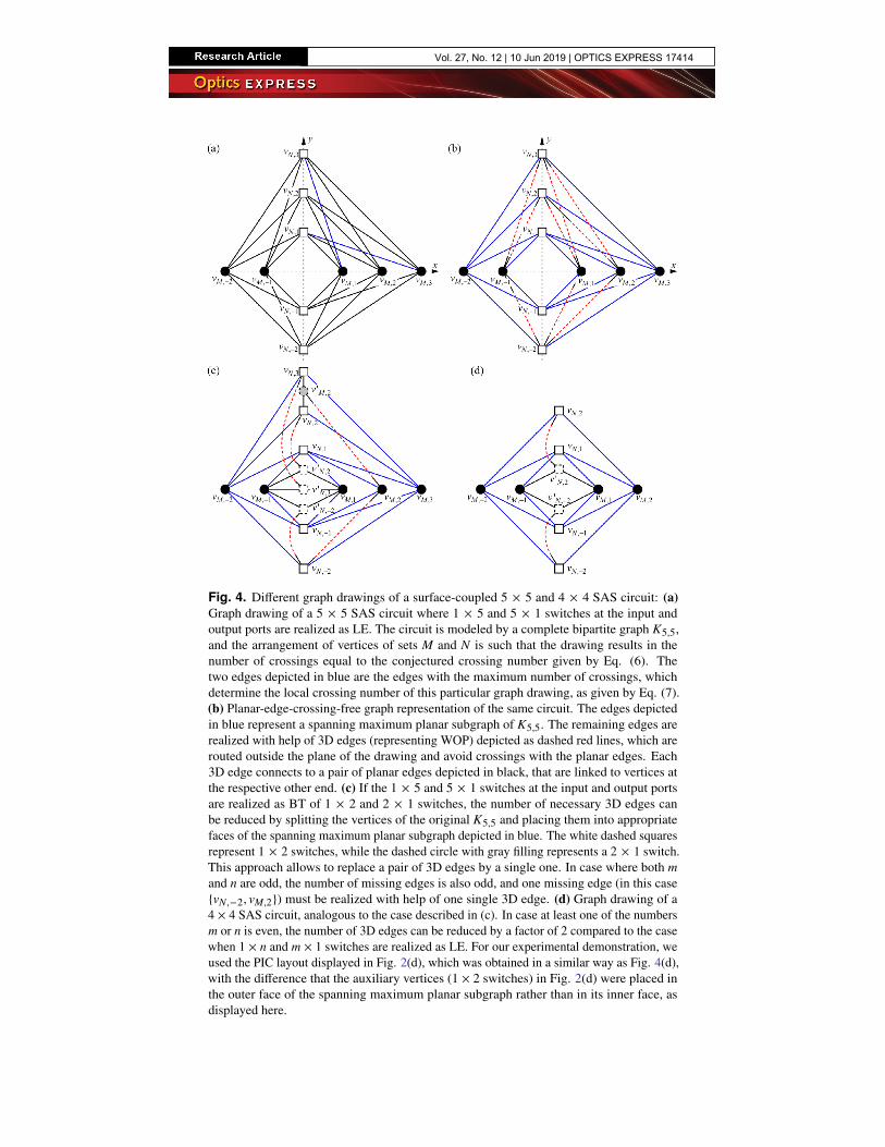
Fig. 4. Different graph drawings of a surface-coupled 5 × 5 and 4 × 4 SAS circuit: (a)Graph drawing of a 5 × 5 SAS circuit where 1 × 5 and 5 × 1 switches at the input andoutput ports are realized as LE. The circuit is modeled by a complete bipartite graph K5,5,and the arrangement of vertices of sets M and N is such that the drawing results in thenumber of crossings equal to the conjectured crossing number given by Eq. (6). Thetwo edges depicted in blue are the edges with the maximum number of crossings, whichdetermine the local crossing number of this particular graph drawing, as given by Eq. (7).(b) Planar-edge-crossing-free graph representation of the same circuit. The edges depictedin blue represent a spanning maximum planar subgraph of K5,5. The remaining edges arerealized with help of 3D edges (representing WOP) depicted as dashed red lines, which arerouted outside the plane of the drawing and avoid crossings with the planar edges. Each3D edge connects to a pair of planar edges depicted in black, that are linked to vertices atthe respective other end. (c) If the 1 × 5 and 5 × 1 switches at the input and output portsare realized as BT of 1 × 2 and 2 × 1 switches, the number of necessary 3D edges canbe reduced by splitting the vertices of the original K5,5 and placing them into appropriatefaces of the spanning maximum planar subgraph depicted in blue. The white dashed squaresrepresent 1 × 2 switches, while the dashed circle with gray filling represents a 2 × 1 switch.This approach allows to replace a pair of 3D edges by a single one. In case where both mand n are odd, the number of missing edges is also odd, and one missing edge (in this case{vN,−2, vM,2}) must be realized with help of one single 3D edge. (d) Graph drawing of a4 × 4 SAS circuit, analogous to the case described in (c). In case at least one of the numbersm or n is even, the number of 3D edges can be reduced by a factor of 2 compared to the casewhen 1 × n and m × 1 switches are realized as LE. For our experimental demonstration, weused the PIC layout displayed in Fig. 2(d), which was obtained in a similar way as Fig. 4(d),with the difference that the auxiliary vertices (1 × 2 switches) in Fig. 2(d) were placed inthe outer face of the spanning maximum planar subgraph rather than in its inner face, asdisplayed here.
Vol. 27, No. 12 | 10 Jun 2019 | OPTICS EXPRESS 17414

links two planar edges, each of which is connected to another vertex at its respective other end.In order to estimate the number of necessary 3D edges, we first construct a spanning maximumplanar subgraph of Km,n, which has 2m + 2n – 4 edges [34]. We do it by connecting each of thevertices vM,−bm/2c , vM,dm/2e , vN,−1, and vN,1 to each vertex of the opposite set, see Fig. 4(b). Theremaining
µ(surf)m,n = mn − (2m + 2n − 4) = (m − 2)(n − 2) (8)
edges can be realized using 3D edges. For m = n, Eq. (8) reduces to Eq. (3). The concept isillustrated in Fig. 4(b) for the case of K5,5. The edges of the spanning maximum planar subgraphare depicted in blue, the 3D edges in red (dashed), while the planar edges that connect the 3Dedges to the vertices are depicted in black. The red dashed lines are, in fact, vertical projectionsof 3D edges on the 2D drawing plane.
Note that the planar projections of the 3D edges on the drawing plane may cross each other.This, however, does not mean that the two 3D edges cross in 3D space – two freeform WOPcan always be 3D-printed such that one passes over the other, and the corresponding 3D edgescan be routed analogously. Furthermore, by appropriate routing of the planar and 3D edges, thecrossings of projections of 3D edges on the drawing plane can be avoided. Figure 4(b) showshow a possible crossing of projections of two 3D edges between pairs of vertices {vN,2, vM,2}
and {vN,3, vM,1} has been avoided by making the planar waveguide that connects vN,2 to thecorresponding 3D edge sufficiently long such that it passes underneath the 3D edge betweenthe pair of vertices {vN,3, vM,1}. We believe that this approach might be generalized to avoidcrossings of projections of 3D edges for general complete bipartite graphs Km,n – a general proofwould need further investigation and is beyond the scope of this paper.
If the 1 × n and m × 1 switches at the input and output ports are realized as BT of 1 × 2 and2 × 1 switches rather than as LE, we can further reduce the number of 3D edges. We will splitthe analysis into two cases: when both m and n are odd, and when at least one of them is even.Furthermore, we will only analyze cases where both m and n are ≥ 3 since otherwise, accordingto Kuratowski’s theorem [40], the complete bipartite graph Km,n is planar. If both m and n areodd, we do the following steps:
Step 1: Construct the spanning maximum planar subgraph of Km,n as described above. Theedges of this subgraph are depicted in blue in Fig. 4(c) for the case of K5,5 (m = n = 5). Thissubgraph has all faces determined by four vertices (two from set M and two from set N) andfour edges. There are (m – 3) vertices of set M whose x-coordinates lie between −bm/2c + 1and dm/2e − 2 inclusive, and they can be divided into (m – 3)/2 distinct two-element subsetsof vertices (because m – 3 is even, and therefore divisible by two): {vM,−bm/2c+1, vM,−bm/2c+2},{vM,−bm/2c+3, vM,−bm/2c+4}, . . . , {vM,dm/2e−3, vM,dm/2e−2}. Each of these (m – 3)/2 pairs of ver-tices of set M together with the pair of vertices {vN,−1, vN,1} of set N, define (m – 3)/2 faces:{vM,−bm/2c+1, vN,−1, vM,−bm/2c+2, vN,1}, {vM,−bm/2c+3, vN,−1, vM,−bm/2c+4, vN,1}, . . . , {vM,dm/2e−3,vN,−1, vM,dm/2e−2, vN,1}. For m = 3 there are no such faces. For m = 5, there is only one suchface {vM,−bm/2c+1, vN,−1, vM,dm/2e−2, vN,1} = {vM,−1, vN,−1, vM,1, vN,1}, see Fig. 4(c). Note thatthe results of the expressions −bm/2c + i and dm/2e − j in the subscripts of labels of vertices ofset M indicate the x-coordinates of the vertices. Since there is no vertex at x = 0, not a singleexpression is allowed to result in zero. Therefore, we restrict the values of integers i and j toi = 1, 2, . . . , bm/2c − 1, and j = dm/2e − 1, dm/2e − 2, . . . , 2 (the expression −bm/2c + i is usedfor vertices on the negative side of the x-axis, while the expression dm/2e − j is used for verticeson the positive side of the x-axis).
Step 2: Let us put an auxiliary vertex v′N,dn/2e inside the face defined by vertices{vM,−bm/2c+1, vN,−1, vM,−bm/2c+2, vN,1}. We can connect the auxiliary vertex v′N,dn/2e to vertexvN,dn/2e with a 3D edge, and the same auxiliary vertex to vertices vM,−bm/2c+1 and vM,−bm/2c+2with two planar edges. The auxiliary vertex is the place where we put a 2 × 1 switch, which is apart of the BT m × 1 switch at the vertex vN,dn/2e . In this way, we can replace two 3D edges
Vol. 27, No. 12 | 10 Jun 2019 | OPTICS EXPRESS 17415

that would otherwise separately connect vertex vN,dn/2e to vertices vM,−bm/2c+1 and vM,−bm/2c+2.The auxiliary vertex v′N,dn/2e and the two planar edges that connect it to vertices vM,−bm/2c+1and vM,−bm/2c+2 split the original face {vM,−bm/2c+1, vN,−1, vM,−bm/2c+2, vN,1} into two faces{vM,−bm/2c+1, vN,−1, vM,−bm/2c+2, v′N,dn/2e } and {vM,−bm/2c+1, vN,1, vM,−bm/2c+2, v′N,dn/2e }. We putan additional auxiliary vertex v′N,dn/2e−1 to any of the two new faces, and we connect it to vertexvN,dn/2e−1 with a 3D edge and to vertices vM,−bm/2c+1 and vM,−bm/2c+2 with two planar edges.We repeat the procedure for all vertices of set N, except for vertices vN,−1 and vN,1, which arealready connected to all vertices of set M. In this way, we connect both vertices of the pair{vM,−bm/2c+1, vM,−bm/2c+2} to all vertices of set N. We apply the same algorithm to connect thepairs of vertices {vM,−bm/2c+3, vM,−bm/2c+4}, . . . , {vM,dm/2e−3, vM,dm/2e−2} to all vertices of set N.This step has been illustrated in Fig. 4(c) where auxiliary vertices v′N,3, v′N,2, and v′N,−2 have beenplaced inside the face {vM,−1, vN,−1, vM,1, vN,1}, connected to vertices vN,3, vN,2, and vN,−2 by 3Dedges, respectively, and to vM,−1 and vM,1 by planar edges. For m = 3, Step 2 is skipped.
Step 3: So far, we connected all vertices of set M to all vertices of set N, except for ver-tex vM,dm/2e−1 that is connected only to vN,−1 and vN,1 and still needs to be connected to theremaining (n – 2) vertices of set N. There are dn/2e − 1 such vertices on the positive sideof the y-axis: vN,dn/2e , vN,dn/2e−1, . . . , vN,2, and bn/2c − 1 on the negative side of the y-axis:vN,−2, vN,−3, . . . , vN,−bn/2c . Depending on n, one of these two numbers is even, and the otheris odd. If dn/2e − 1 is even and bn/2c − 1 is odd, then each of the following pairs of vertices{vN,dn/2e , vN,dn/2e−1}, . . . , {vN,3, vN,2}, {vN,−2, vN,−3}, . . . , {vN,−bn/2c+2, vN,−bn/2c+1} together withthe pair of vertices {vM,−bm/2c , vM,dm/2e } define one face. In each of these faces, we can placeone auxiliary vertex v′M,dm/2e−1, v′′M,dm/2e−1, v′′′M,dm/2e−1, . . . , see Fig. 4(c), where there is onlyone such auxiliary vertex v′M,dm/2e−1 = v′M,2. Each of these auxiliary vertices can be connectedto vM,dm/2e−1 by a 3D edge and to the respective pair of vertices of set N (that define the facein which the auxiliary vertex is placed) by two planar edges. After this step, there will beonly one missing edge between vertices vM,dm/2e−1 and vN,−bn/2c , and we directly connectthese two vertices by a single 3D edge, see Fig. 4(c). Similarly, if dn/2e − 1 is odd andbn/2c − 1 is even, we can group the vertices of set N into pairs as {vN,dn/2e−1, vN,dn/2e−2}, . . . ,{vN,3, vN,2}, {vN,−2, vN,−3}, . . . , {vN,−bn/2c+1, vN,−bn/2c } which would define faces together withthe pair of vertices {vM,−bm/2c , vM,dm/2e }. After placing and connecting auxiliary vertices asdescribed, the only missing edge would be between vM,dm/2e−1 and vN,dn/2e , and we wouldconnect them by one 3D edge.
The case when at least one of the numbers m and n is even is simpler. We can assumewithout loss of generality that m is even and n is odd. By constructing the spanning maxi-mum planar subgraph of Km,n as described above, we will get a subgraph where each of thefollowing (m – 2)/2 pairs of vertices {vM,−bm/2c+1, vM,−bm/2c+2}, {vM,−bm/2c+3, vM,−bm/2c+4}, . . . ,{vM,dm/2e−2, vM,dm/2e−1} together with the pair of vertices {vN,−1, vN,1} define one face. Afterperforming Step 2 as described above, we will connect all vertices of set M to all vertices of setN. Figure 4(d) shows an example of the result of the algorithm for the case of K4,4.
The described algorithm allows to replace two missing planar edges by one 3D edge. Thenumber of necessary 3D edges hence amounts to
µ(surf, BT)m,n =
⌈(m − 2)(n − 2)
2
⌉, (9)
which reduces to Eq. (4) for m = n. The ceiling function in Eq. (9) is used to include the casewhen the number of missing edges is odd (both m and n are odd) and not divisible by two (onesingle missing edge needs to be realized with one single 3D edge). This algorithm is just anexample and not the unique way of constructing a layout that results in the number of 3D edgesgiven by Eq. (9): For example, in Step 1 we could construct the spanning maximum planarsubgraph in a different way and then modify Steps 2 and 3 accordingly.
Vol. 27, No. 12 | 10 Jun 2019 | OPTICS EXPRESS 17416

It should be pointed out that Eq. (9) does not necessarily give the minimum number ofnecessary 3D edges, but an upper bound. In our construction we started from the spanningmaximum planar subgraph, and we split some vertices in two by introducing auxiliary vertices.We did, however, not show that the spanning maximum planar subgraph of Km,n is the optimalway to start with. We could have also started with a non-maximum planar subgraph and couldhave used larger split ratio switches 1 × n′, n′ < n and 1 × m′, m′ < m, and place them in theauxiliary vertices. Furthermore, the graph model of the device where 1 × n and m × 1 switchesat the input and output ports are realized as BT of 1 × 2 and 2 × 1 switches, is not a completebipartite graph Km,n. The crossing number of the SAS circuit realized with such an approach issubject to ongoing investigations.
Appendix C: Facet-coupled SAS circuits
C.1. Facet-coupled SAS realized in single-layer and hybrid 2D/3D photonic integration
For facet-coupled SAS circuits, all input and output ports are implemented by waveguide facetsarranged along the chip boundaries, making it impossible to route waveguides “behind” the ports,i.e., between the ports and the chip boundary. In the graph drawing of the circuit, all verticesrepresenting input and output ports must hence be placed on a closed curve that represents theboundary of the chip surface, and no waveguide (graph edge) routing outside the area enclosedby the curve is allowed. In addition, in contrast to surface coupling, the graph of a facet-coupledSAS is not anymore a complete bipartite graph: For the case of surface coupling, a port and theassociated 1 × n or m × 1 switch can be combined into a single vertex, whereas facet-coupledcircuits must be represented by a first kind of vertices for the switches and a second kind ofvertices for the ports, which must be placed onto the boundary curve. Every port vertex must beconnected to the associated switch by a graph edge that represents the access waveguide. Thisresults in a 3-partite graph, which comprises three parties of vertices represented by the ports, the1 × n switches, and the m × 1 switches, and which is not complete. For a general description offacet-coupled SAS circuits, we can hence not resort any more to the existing theory of completebipartite graphs. This renders theoretical assessment of the topologies more difficult and requiressimplifying assumptions for quantifying the numbers of WGX or WOP. Nevertheless, we believethat non-planar facet-coupled SAS circuits can also greatly benefit from replacing WGX byWOP.
To support this claim, we first consider the basic non-optimized representation of a 4 × 4SAS circuit, see Fig. 5(a). This representation relies on the same simplistic approach as thesurface-coupled SAS circuit that is sketched in Fig. 2(a). In this approach, each pair of verticesof set M is connected by four edges to each pair of vertices of set N, and the four edges makeexactly one crossing. The number of crossings is therefore equal to the product of numbers ofways to choose two-element subsets of M and N and amounts to
η(facet, basic)m,n =
m
2
n
2
=
(m(m − 1)
2
) (n(n − 1)
2
), (10)
which reduces to Eq. (1) for the case of m = n. Interleaving the input and output ports alongthe boundary line allows to reduce this number, see Fig. 5(b). In this case, we can simplify thetheoretical assessment to finding the outerplanar crossing number of a complete bipartite graph.This can be seen if we look at the blue dashed line in Fig. 5(b): All vertices representing 1 × nand m × 1 switches are placed on it, and all edges are routed inside the area bounded by it. Notethat this implementation is not yet optimal since it does not exploit the possibility to reduce thenumber of WGX by routing waveguides between the ports and the corresponding 1 × n or m ×
Vol. 27, No. 12 | 10 Jun 2019 | OPTICS EXPRESS 17417

1 switches. For the case of n being an integer multiple of m, the outerplanar crossing number ofa complete bipartite graph Km,n. is obtained when the vertices of set M are evenly interleavedbetween the vertices of set N and amounts to [43]
η(facet)m,n =
112
n(m − 1)(2mn − 3m − n). (11)
Fig. 5. Different graph drawings of a facet-coupled 4 × 4 SAS circuit: A first set of vertices(rectangles and half circles) is used to represent facet-coupled optical input and outputports, and a second kind of vertices (squares and full circles) represents the 1 × n or m × 1switches. Each port vertex is connected to the associated switch vertex by a graph edge thatrepresents the access waveguide (a) Simplistic non-optimum graph representation based onthe same approach as the surface-coupled SAS circuit shown in Fig. 2(a). Input and outputports are clustered into two groups of neighboring vertices along the chip boundary. For a 4× 4 SAS circuit, 36 WGX are required. (b) By interleaving the input and output ports alongthe chip boundary, the number of crossings can be reduced, leading to a total number of 16WGX for a 4 × 4 SAS circuit. (c) The number of crossings can also be reduced by allowingrouting of waveguides between the ports and the corresponding 1 × n and n × 1 switches,leading to a total number of 20 WGX for the depicted graph drawing. (d) Circuit layoutobtained by combining interleaving of input and output ports with routing of waveguidesbetween the ports and the corresponding switches, leading to a total number of 12 WGX.
Vol. 27, No. 12 | 10 Jun 2019 | OPTICS EXPRESS 17418

For the case m = n, this reduces to
η(facet)n,n =
16
n2(n − 1)(n − 2), (12)
Which scales with n4/6 for large n. The associated numbers of WGX for switches implementedas LE are listed in the second column of Table 2. Further layout optimization steps may involverouting of waveguides between the ports and the corresponding switches, possibly in combinationwith interleaving of the ports along the chip boundary, see Figs. 5(c) and 5(d). Even thoughwe are not aware of any relations specifying the exact crossing numbers of these graphs, wemay still use the number of WGX in the associated surface-coupled SAS as a lower bound.This can be understood by observing that both implementations in Figs. 5(c) and 5(d) contain amaximum bipartite subgraph (indicated in blue) which is equivalent to that of the correspondingsurface-coupled circuit, Fig. 2(b), and which is complemented by additional crossings causedby the access waveguides. The number of WGX still scales with at least n4/16, see Eq. (2).Similarly to the case of surface-coupled SAS, disaggregating the 1 × n and m × 1 switches intoBT of 1 × 2 switches might reduce the number of WGX – this aspect is still under investigation.For the remainder of this section, we rely on Eq. (12) for determining the number of WGX inthe facet-coupled n × n SAS circuit.
Table 2. Quantitative Comparison of n × n Facet-Coupled Switch-and-Select (SAS) CircuitImplementations Based on WGX in Single-Layer Circuits and on WOP in Hybrid 2D/3D Photonic
Integrationa
Total number Maximum number along an optical path
SAS (n × n) WGX (LE) WOP (LE) WOP (BT) WGX (LE) WOP (LE & BT)
4 × 4 16 9 5 4 1
8 × 8 448 49 25 24 1
16 × 16 8 960 225 113 112 1
32 × 32 158 720 961 481 480 1
64 × 64 2 666 496 3 969 1 985 1 984 1
aThe total number of WGX (second column) increases approximately in proportion to n4/6, whereas the number ofWOP scales with n2 for the case of LE switches (third column) and with n2/2 in case the switches are decomposedinto BT of 1 × 2 and 2 × 1 switches (fourth column). The maximum number of WGX along an optical path increasesapproximately in proportion to n2/2 for the case of LE switches (fifth column), whereas the maximum number of WOPalong an optical path is one in both cases of LE and BT switches (sixth column).
For 2D/3D hybrid implementations, the number of WOP in facet-coupled SAS circuits wasanalyzed based on the simplistic layout shown in Fig. 5(a) for cases of LE switches and BTcascaded 1 × 2 switches, see Figs. 6(a) and 6(b). Mathematical details can be found in AppendixC.2. For LE switches, this leads to a total WOP number of
µ(facet)m,n = (m − 1)(n − 1), (13)
which reduces to (n – 1)2 for m = n. For BT switches, the number of WOP amounts to
µ(facet, BT)m,n =
⌈(m − 1)(n − 1)
2
⌉, (14)
i.e., d(n − 1)2/2e for m = n. Hence, in both cases, the number of WOP in the facet-coupledhybrid 2D/3D implementation scales much more favorably than the number of WGX in thecorresponding single-layer SAS circuit, see third and fourth column of Table 2. Note that thisnumber represents an upper bound for the number of WOP, which might be further reduced by
Vol. 27, No. 12 | 10 Jun 2019 | OPTICS EXPRESS 17419

interleaving of ports and by rerouting of connections across the access waveguides, similarlyto the case of the surface-coupled planar circuits shown in Figs. 2(b)–2(d). As in the case ofsurface coupling, the number of WOP along any optical path through the facet-coupled hybrid2D/3D circuit is at most 1, whereas the maximum number of WGX along an optical path in asingle-layer implementation shown in Fig. 5(b) increases in proportion to n2/2. The exact resultfor the maximum number of WGX along any optical path for this implementation is
ξ (facet)m,n = 2
⌊n − 1
2
⌋ ⌈n − 1
2
⌉, (15)
see Section C.2. The corresponding numbers for n = 4, 8, 16, 32, and 64 are indicated in the fifthand sixth column of Table 2. For the implementations shown in Figs. 5(c) and 5(d), we cannotprovide a formula that describes the minimum number of WGX along an optical path.
Fig. 6. Circuit layouts for facet-coupled 2D/3D hybrid 4 × 4 SAS. (a) Simple, but notoptimal layout, where the 1 × 4 and 4 × 1 switches have been realized as LE. The relationfor µ(facet)
n,n represents the exact number of WOP in this simplistic implementation. (b) Bestfound, but not necessarily optimal layout for the case in which the 1 × 4 and 4 × 1 switcheshave been realized as BT of 1 × 2 and 2 × 1 switches. The relation for µ(facet, BT)
n,n is anupper bound for the minimum number of WOP.
C.2. Graph-theoretical models and analysis of facet-coupled m × n SAS circuits
Let us first explain Eq. (15) which is obtained in case of a drawing of the complete bipartitesubgraph Kn,n that results in the outerplanar crossing number – the vertices belonging to differentvertex sets M and N (m = n) are interleaved along the boundary curve. This subgraph is depictedin blue in Fig. 5(b) for n = 5. The concept of this layout is illustrated in Fig. 7, which showsgraph drawings of a complete bipartite graph Kn,n with interleaved vertices of two differentvertex sets along the boundary (dashed circular line). Each edge divides the bounded area intwo parts, and the largest number of crossings will be on an edge {vM,i, vN,i} that divides thearea such that the numbers of vertices in both parts are as much equal as possible. If n is odd, itis possible to find an edge that divides the bounded area such that both parts have exactly thesame number of vertices; on the other hand, if n is even, one part will have one more vertex of
Vol. 27, No. 12 | 10 Jun 2019 | OPTICS EXPRESS 17420

each vertex set than the other part. Both cases are illustrated in Fig. 7 – the edge {vM,i, vN,i} isdepicted in blue. For both cases, edge {vM,i, vN,i} divides the area such that one part containsb(n − 1)/2c and the other d(n − 1)/2e vertices of each vertex set. That means that edge {vM,i, vN,i}
is crossed by b(n − 1)/2c d(n − 1)/2e edges connecting b(n − 1)/2c vertices of set M in the firstpart to d(n − 1)/2e vertices of set N in the second part, and the same number of edges connectingb(n − 1)/2c vertices of set N in the first part to d(n − 1)/2e vertices of set M in the second part.From here follows the result of Eq. (15).
Fig. 7. Drawings of complete bipartite graphs Kn,n with all vertices placed on the closedboundary curve (dashed circular line), and the vertices of two different sets being interleavedalong the boundary. Equation (15) gives the local crossing number of such drawing, whichoccurs along the blue edges that divide the boundary area in two parts such that the numberof vertices in both parts is as much balanced as possible. (a) In case n is odd (here: n = 5),both parts contain the same number of vertices. (b) In case n is even (here: n = 6), there isone more vertex of each vertex set in one part.
In order to estimate the number of necessary WOP (3D edges), we will use the simplisticlayout shown in Fig. 5(a). It is sufficient to consider a drawing of Km,n with all vertices placedon a closed boundary curve, since access waveguides do not have any crossings. We constructa corresponding graph drawing by placing all m vertices of set M: vM,1, vM,2, . . . , vM,m on thex-axis of the 2D Cartesian coordinate system in points x = 1, 2, . . . , m, see Fig. 8(a) for anillustration of the case of K4,4. Similarly, we place all n vertices of set N: vN,1, vN,2, . . . , vN,n onthe y-axis in points y = 1, 2, . . . , n. Finally, we connect all vertices of set M to all vertices ofset N by mn line segments. The boundary curve can be for example a rectangle that is orientedalong the x and the y axis, as depicted in green in Fig. 8(a). The total number of crossings isequivalent to the one given by Eq. (10) – it takes four edges and one crossing to connect eachpossible pair of vertices of set M to each possible pair of vertices of set N. In order to estimatethe number of necessary 3D edges, we first construct a spanning planar subgraph of Km,n, byconnecting vertices vM,1 and vN,n to all vertices of the opposite vertex sets, Fig. 8(b). Thissubgraph evidently has m + n – 1 edges, and the number of missing edges is therefore equal tomn – (m + n – 1) = (m – 1)(n – 1), which leads to Eq. (13). These edges can be realized with helpof 3D edges, illustrated by dashed red lines in Fig. 8(b).
Similarly to the case of surface coupled SAS described in Appendix B, if the 1 × n andm × 1 switches at the input and output ports are BT of 1 × 2 and 2 × 1 switches, the number ofnecessary 3D edges reduces. We will split the analysis into two cases: when both m and n are
Vol. 27, No. 12 | 10 Jun 2019 | OPTICS EXPRESS 17421

Fig. 8. Different graph drawings of a simplistic model of a facet-coupled 4 × 4 and 5 × 4SAS circuit: (a) Graph drawing of a 4 × 4 SAS circuit where 1 × 4 and 4 × 1 switches atthe input and output ports are LE. (b) Planar-edge-crossing-free graph representation ofthe same circuit. The edges depicted in blue represent a spanning planar subgraph of K4,4.The remaining edges are realized with help of 3D edges (representing WOP) depicted asdashed red lines. The 3D edges connect to planar edges depicted in black that connect tothe vertices in the drawing plane. (c) If the 1 × 5 and 5 × 1 switches at the input and outputports are realized as BT of 1 × 2 and 2 × 1 switches, the number of necessary 3D edges canbe reduced by splitting the vertices of the original K4,4 and by placing them into appropriateareas which are defined by the edges of the spanning planar subgraph (blue) and by the xor y coordinate axes. The white dashed squares represent 1 × 2 switches, while the filledgray circle represents a 2 × 1 switch. This approach allows to replace two 3D edges byone. In case where both m and n are even, the number of missing edges is odd, therefore,one missing edge (here: {vN,3, vM,4}) must be realized with help of one single 3D edge (d)Graph drawing of a 5 × 4 SAS circuit, analogous to the case described in (c). In case atleast one of the numbers m or n is odd, the number of 3D edges can be reduced exactly 2times compared to the case when 1 × n and m × 1 switches are realized as LE.
Vol. 27, No. 12 | 10 Jun 2019 | OPTICS EXPRESS 17422

even, and when at least one of them is odd. If both are even, the analysis comprises the followingsteps:
Step 1: Construct a spanning planar subgraph of Km,n as described above. Each pair of vertices{vM,2, vM,3}, {vM,4, vM,5}, . . . , {vM,m−2, vM,m−1}, together with vertex vN,n defines one area, whichis bounded by two edges between vN,n and the two vertices of set M and a portion of the x-axisbetween the two vertices of set M. This is illustrated on an example of K4,4 in Fig. 8(c).
Step 2: Put an auxiliary vertex v′N,1 inside the area defined by vertices {vM,2, vM,3, vN,n}, seeFig. 8(c). We can connect the auxiliary vertex v′N,1 and vertex vN,1 by a 3D edge, and the sameauxiliary vertex and vertices vM,2 and vM,3 by planar edges. Similarly to the case of surface-coupled SAS, we continue adding auxiliary vertices v′N,2, v′N,3, . . . , v′N,n−1, to the same area untilwe connect all vertices of set N to vM,2 and vM,3. We then continue with the same procedure for thefollowing areas defined by groups of three vertices: {vM,4, vM,5, vN,n}, . . . , {vM,n−2, vM,n−1, vN,n}.
Step 3: In this fashion, we will connect all vertices of set M to all vertices of set N, exceptfor vertex vM,m that is connected only to vN,n. However, each of the following pairs of vertices{vN,1, vN,2}, . . . , {vN,n−3, vN,n−2}, together with vertex vM,1 define one area bounded by two edges(between vM,1 and the two vertices of set N) and a portion of the y-axis between the two verticesof set N. In each of these areas, we can place one auxiliary vertex: v′M,m, v′′M,m, v′′′M,m, . . . Eachof these auxiliary vertices can be connected to vM,m by a 3D edge, and to the respective pair ofvertices of set N that define the area in which the auxiliary vertex is placed by two planar edges.After this step, there will be only one missing edge between vertices vM,m and vN,n−1, and wedirectly connect these two vertices by a single 3D edge, see Fig. 8(c).
In case when at least one of the numbers m and n is odd, we can assume without loss ofgenerality that m is odd, and n is even. By executing Step 1 as described above, we willget a subgraph where each of the pairs of vertices {vM,2, vM,3}, {vM,4, vM,5}, . . . , {vM,m−1, vM,m},together with vertex vN,n defines one area bounded by two edges (between vN,n and the twovertices of set M) and a portion of the x-axis between the two vertices of set M. After performingStep 2 as described above, we will connect all vertices of set M to all vertices of set N. This caseis illustrated on an example of K5,4 in Fig. 8(d). For at least one of the numbers m and n beingodd, the number of missing edges is even, and we can replace two missing planar edges by one3D edge. Combining the two cases leads to Eq. (14).
Funding
Erasmus Mundus Joint Doctorate program EUROPHOTONICS (159224-1-2009-1-FR-ERAMUNDUS-EMJD); Deutsche Forschungsgemeinschaft (DFG), Wave Phenomena, Project C4(CRC 1173); Bundesministerium für Bildung und Forschung (BMBF), Project PRIMA (13N14630);Alfried Krupp von Bohlen und Halbach-Stiftung Foundation; Helmholtz International ResearchSchool for Teratronics (HIRST); H2020 Photonic Packaging Pilot Line ’PIXAPP’ (731954);H2020 European Research Council (ERC) Consolidator Grant ‘TeraSHAPE’ (773248); Karl-sruhe Nano-Micro Facility (KNMF); Karlsruhe School of Optics and Photonics (KSOP).
Acknowledgments
We acknowledge fruitful discussions with Maria Axenovich (Institute of Algebra and Geometry(IAG), Karlsruhe Institute of Technology (KIT), Germany). Portions of this work were presentedat the European Conference on Optical Communications (ECOC) in 2016 [24].
References1. J. Sun, E. Timurdogan, A. Yaacobi, E. S. Hosseini, and M. R. Watts, “Large-scale nanophotonic phased array,”
Nature 493(7431), 195–199 (2013).2. T. J. Seok, N. Quack, S. Han, R. S. Muller, and M. C. Wu, “Large-scale broadband digital silicon photonic switches
with vertical adiabatic couplers,” Optica 3(1), 64–70 (2016).
Vol. 27, No. 12 | 10 Jun 2019 | OPTICS EXPRESS 17423

3. M. Hochberg, N. C. Harris, R. Ding, Y. Zhang, A. Novack, Z. Xuan, and T. Baehr-Jones, “Silicon photonics: Thenext fabless semiconductor industry,” IEEE Solid-State Circuits Mag. 5(1), 48–58 (2013).
4. L. Chrostowski and M. Hochberg, Silicon Photonics Design (Cambridge University, 2015).5. Y. Ma, Y. Zhang, S. Yang, A. Novack, R. Ding, A. E.-J. Lim, G.-Q. Lo, T. Baehr-Jones, and M. Hochberg,
“Ultralow loss single layer submicron silicon waveguide crossing for SOI optical interconnect,” Opt. Express 21(24),29374–29382 (2013).
6. Y. Zhang, A. Hosseini, X. Xu, D. Kwong, and R. T. Chen, “Ultralow-loss silicon waveguide crossing using Blochmodes in index-engineered cascaded multimode-interference couplers,” Opt. Lett. 38(18), 3608–3611 (2013).
7. Y. Liu, J. M. Shainline, X. Zeng, and M. A. Popovic, “Ultra-low-loss CMOS-compatible waveguide crossing arraysbased on multimode Bloch waves and imaginary coupling,” Opt. Lett. 39(2), 335–338 (2014).
8. L. Chen and Y. K. Chen, “Compact, low-loss and low-power 8×8 broadband silicon optical switch,” Opt. Express20(17), 18977–18985 (2012).
9. M. R. Garey and D. S. Johnson, “Crossing number is NP-complete,” SIAM J. Alg. Disc. Meth. 4(3), 312–316 (1983).10. L. A. Székely, “Turán’s brick factory problem: The status of the conjectures of Zarankiewicz and Hill,” in Graph
Theory–Favorite Conjectures and Open Problems–1, R. Gera, S. Hedetniemi, and C. Larson, eds. (SpringerInternational Publishing, 2016).
11. C. Zarankiewicz, “On a problem of P. Turan concerning graphs,” Fundam. Math. 41(1), 137–145 (1955).12. I. Kaminow, T. Li, and A. Willner, Optical Fiber Telecommunications, Volume VIB, 6th edition (Elsevier Science
Publishing Company, Inc., 2013).13. F. Chang, K. Onohara, and T. Mizuochi, “Forward error correction for 100 G transport networks,” IEEE Commun.
Mag. 48(3), S48–S55 (2010).14. K. Itoh, Y. Kuno, Y. Hayashi, J. Suzuki, N. Hojo, T. Amemiya, N. Nishiyama, and S. Arai, “Crystalline/amorphous
Si integrated optical couplers for 2D/3D interconnection,” IEEE J. Sel. Top. Quantum Electron. 22(6), 255–263(2016).
15. J. Chiles, S. Buckley, N. Nader, S. W. Nam, R. P. Mirin, and J. M. Shainline, “Multi-planar amorphous siliconphotonics with compact interplanar couplers, cross talk mitigation, and low crossing loss,” APL Photonics 2(11),116101 (2017).
16. K. Shang, S. Pathak, B. Guan, G. Liu, and S. J. B. Yoo, “Low-loss compact multilayer silicon nitride platform for 3Dphotonic integrated circuits,” Opt. Express 23(16), 21334–21342 (2015).
17. K. Shang, S. Pathak, G. Liu, S. Feng, S. Li, W. Lai, and S. J. B. Yoo, “Silicon nitride tri-layer vertical Y-junction and3D couplers with arbitrary splitting ratio for photonic integrated circuits,” Opt. Express 25(9), 10474–10483 (2017).
18. A. M. Jones, C. T. DeRose, A. L. Lentine, D. C. Trotter, A. L. Starbuck, and R. A. Norwood, “Ultra-low crosstalk,CMOS compatible waveguide crossings for densely integrated photonic interconnection networks,” Opt. Express21(10), 12002–12013 (2013).
19. W. D. Sacher, Y. Huang, G.-Q. Lo, and J. K. Poon, “Multilayer silicon nitride-on-silicon integrated photonic platformsand devices,” J. Lightwave Technol. 33(4), 901–910 (2015).
20. K. Suzuki, R. Konoike, K. Tanizawa, S. Suda, H. Matsuura, K. Ikeda, S. Namiki, and H. Kawashima, “Ultralow-crosstalk and broadband multi-port optical switch using SiN/Si double-layer platform,” in Opto-Electronics andCommunications Conference (OECC) and Photonics Global Conference (PGC) (IEEE, 2017), pp. 1–2.
21. W. D. Sacher, J. C. Mikkelsen, P. Dumais, J. Jiang, D. Goodwill, X. Luo, Y. Huang, Y. Yang, A. Bois, P. G.-Q. Lo, E.Bernier, and J. K. S. Poon, “Tri-layer silicon nitride-on-silicon photonic platform for ultra-low-loss crossings andinterlayer transitions,” Opt. Express 25(25), 30862–30875 (2017).
22. Q. Cheng, L. Y. Dai, M. Bahadori, N. C. Abrams, P. E. Morrissey, M. Glick, P. O’Brien, and K. Bergman,“Si/SiN microring-based optical router in switch-and-select topology,” in 44th European Conference on OpticalCommunications (ECOC) (IEEE, 2018), pp. 1–3.
23. W. D. Sacher, J. C. Mikkelsen, Y. Huang, J. C. C. Mak, Z. Yong, X. Luo, Y. Li, P. Dumais, J. Jiang, D. Goodwill, E.Bernier, P. G.-Q. Lo, and J. K. S. Poon, “Monolithically integrated multilayer silicon nitride-on-silicon waveguideplatforms for 3-D photonic circuits and devices,” Proc. IEEE 106(12), 2232–2245 (2018).
24. A. Nesic, M. Blaicher, T. Hoose, M. Lauermann, Y. Kutuvantavida, W. Freude, and C. Koos, “Hybrid 2D/3D photonicintegration for non-planar circuit topologies,” in 42nd European Conference on Optical Communications (ECOC)(IEEE, 2016), paper W.3.F.4.
25. M. Deubel, G. von Freymann, M. Wegener, S. Pereira, K. Busch, and C. M. Soukoulis, “Direct laser writing ofthree-dimensional photonic-crystal templates for telecommunications,” Nat. Mater. 3(7), 444–447 (2004).
26. N. Lindenmann, G. Balthasar, D. Hillerkuss, R. Schmogrow, M. Jordan, J. Leuthold, W. Freude, and C. Koos,“Photonic wire bonding: a novel concept for chip-scale interconnects,” Opt. Express 20(16), 17667–17677 (2012).
27. N. Lindenmann, S. Dottermusch, M. L. Goedecke, T. Hoose, M. R. Billah, T. P. Onanuga, A. Hofmann, W. Freude,and C. Koos, “Connecting silicon photonic circuits to multicore fibers by photonic wire bonding,” J. LightwaveTechnol. 33(4), 755–760 (2015).
28. M. R. Billah, M. Blaicher, T. Hoose, P.-I. Dietrich, P. Marin-Palomo, N. Lindenmann, A. Nesic, A. Hofmann, U.Troppenz, M. Moehrle, S. Randel, W. Freude, and C. Koos, “Hybrid integration of silicon photonics circuits and InPlasers by photonic wire bonding,” Optica 5(7), 876–883 (2018).
29. T. Hoose, M. Billah, M. Blaicher, P. Marin, P.-I. Dietrich, A. Hofmann, U. Troppenz, M. Moehrle, N. Lindenmann,M. Thiel, P. Simon, J. Hoffmann, M. L. Goedecke, W. Freude, and C. Koos, “Multi-Chip integration by photonic wire
Vol. 27, No. 12 | 10 Jun 2019 | OPTICS EXPRESS 17424

bonding: connecting surface and edge emitting lasers to silicon chips,” in Optical Fiber Communications Conferenceand Exhibition (OFC) (IEEE, 2016), pp. 1–3.
30. C. Galland, A. Novack, Y. Liu, R. Ding, M. Gould, T. Baehr-Jones, Q. Li, Y. Yang, Y. Ma, Y. Zhang, K. Padmaraju, K.Bergmen, A. E.-J. Lim, G.-Q. Lo, and M. Hochberg, “A CMOS-compatible silicon photonic platform for high-speedintegrated opto-electronics,” Proc. SPIE 8767, 87670G (2013).
31. T. Yoshida, S. Tajima, R. Takei, M. Mori, N. Miura, and Y. Sakakibara, “Vertical silicon waveguide coupler bent byion implantation,” Opt. Express 23(23), 29449–29456 (2015).
32. M. Blaicher, M. R. Billah, T. Hoose, P.-I. Dietrich, A. Hofmann, S. Randel, W. Freude, and C. Koos, “3D-Printedultra-broadband highly efficient out-of-plane coupler for photonic integrated circuits,” in Conference on Lasers andElectro-Optics (CLEO) (Optical Society of America, 2018), paper STh1A.1.
33. E. de Klerk, J. Maharry, D. V. Pasechnik, R. B. Richter, and G. Salazar, “Improved bounds for the crossing numbersof Km,n and Kn,” SIAM J. Discrete Math. 20(1), 189–202 (2006).
34. A. Errera, “Un théorème sur les liaisons,” C. R. Acad. Sci. Paris 177, 489–491 (1923).35. B. G. Lee and N. Dupuis, “Silicon photonic switch fabrics: technology and architecture,” J. Lightwave Technol.
37(1), 6–20 (2019).36. Y. Nasu, M. Kohtoku, Y. Hibino, and Y. Inoue, “Waveguide interconnection in silica-based planar lightwave circuit
using femtosecond laser,” J. Lightwave Technol. 27(18), 4033–4039 (2009).37. W. Song, R. Gatdula, S. Abbaslou, M. Lu, A. Stein, W. Y.-C. Lai, J. Provine, R. F. W. Pease, D. N. Christodoulides,
and W. Jiang, “High-density waveguide superlattices with low crosstalk,” Nat. Commun. 6(1), 7027 (2015).38. J. Pfeifle, L. Alloatti, W. Freude, J. Leuthold, and C. Koos, “Silicon-organic hybrid phase shifter based on a slot
waveguide with a liquid-crystal cladding,” Opt. Express 20(14), 15359–15376 (2012).39. L. Alloatti, D. Korn, J. Pfeifle, R. Palmer, S. Koeber, M. Baier, R. Schmogrow, S. Diebold, P. Pahl, T. Zwick, H. Yu,
W. Bogaerts, R. Baets, M. Fournier, J. Fedeli, R. Dinu, C. Koos, W. Freude, and J. Leuthold, “Silicon-organic hybriddevices,” Proc. SPIE 8629, 86290P (2013).
40. C. Kuratowski, “Sur le problème des courbes gauches en Topologie,” Fundam. Math. 15(1), 271–283 (1930).41. R. Diestel, Graph Theory, 5th edition (Springer Berlin Heidelberg, 2017).42. M. Schaefer, Crossing Number of Graphs (Taylor & Francis Inc., 2017).43. A. Riskin, “On the outerplanar crossing numbers of Km,n,” Bull. Inst. Combin. Appl. 39, 16–20 (2003).
Vol. 27, No. 12 | 10 Jun 2019 | OPTICS EXPRESS 17425