physics-2015-marking-scheme-panchkula-re ... - · pdf filechandigarh set i page 1 of 18 final...
TRANSCRIPT

Chandigarh SET I Page 1 of 18 Final Draft 17/3/2013 4:50 pm
MARKING SCHEME
SET 55/1/C
Q. No. Expected Answer / Value Points Mar
ks
Total
Marks
Section - A
Set-1, Q1
Set-2, Q5
Set-3, Q2
Power factor = 1
1 1
Set-1, Q2
Set-2, Q4
Set-3, Q5
i) Width of depletion layer will decrease
ii) potential barrier will decrease
iii) junction will conduct
(Any one point)
1 1
Set-1, Q3
Set-2, Q2
Set-3, Q4
𝑃 =∈0 𝑋𝑒𝐸
(Also accept if the student writes P ∝ E or P = 𝑋𝑒 E )
1 1
Set-1, Q4
Set-2, Q3
Set-3, Q1
Mobility is defined as drift velocity per unit electric field
or 𝜇 =𝑣𝑑
𝐸
S.I. Unit - 𝑚2 𝑉𝑠 or 𝐶𝑚 𝑁𝑠
½
½
1
Set-1, Q5
Set-2, Q1
Set-3, Q3
1
𝑓= 𝜇 − 1 (
1
𝑅1−
1
𝑅2)
µ = 1.5
(Award 1 mark even if direct answer is written)
½
½
1
Section - B
Set-1, Q6
Set-2, Q7
Set-3, Q10
Interference
Diffraction
1 All the bright bands are of same
intensity.
Intensity of bright bands goes on
decreasing with increasing order.
2 All the bright bands are of same
width.
Not of same width.
3 Dark bands may be completely dark. Not completely dark.
4 Number of fringes are more. Less in number.
(Any two)
[ Award only 1 mark if student draws intensity distribution curves for both
without writing points]
Or
1×2
2
Two differences between Interference and Diffraction pattern 2
Downloaded From: http://www.cbseportal.com
Downloaded From: http://www.cbseportal.com
Chandigarh SET I Page 2 of 18 Final Draft 17/3/2013 4:50 pm
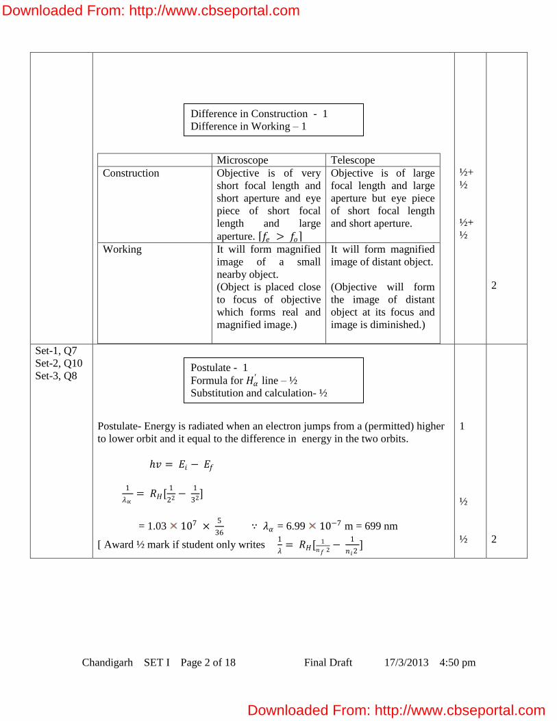
Microscope Telescope
Construction Objective is of very
short focal length and
short aperture and eye
piece of short focal
length and large
aperture. 𝑓𝑒 > 𝑓𝑜
Objective is of large
focal length and large
aperture but eye piece
of short focal length
and short aperture.
Working It will form magnified
image of a small
nearby object.
(Object is placed close
to focus of objective
which forms real and
magnified image.)
It will form magnified
image of distant object.
(Objective will form
the image of distant
object at its focus and
image is diminished.)
½+
½
½+
½
2
Set-1, Q7
Set-2, Q10
Set-3, Q8
Postulate- Energy is radiated when an electron jumps from a (permitted) higher
to lower orbit and it equal to the difference in energy in the two orbits.
ℎ𝑣 = 𝐸𝑖 − 𝐸𝑓
1
𝜆∝ = 𝑅𝐻[
1
22 − 1
32]
= 1.03 107 × 5
36 ∵ 𝜆𝛼 = 6.99 10−7 m = 699 nm
[ Award ½ mark if student only writes 1
𝜆= 𝑅𝐻[ 1
𝑛𝑓 2−
1
𝑛𝑖2 ]
1
½
½
2
Difference in Construction - 1
Difference in Working – 1
Postulate - 1
Formula for 𝐻𝛼′ line – ½
Substitution and calculation- ½
Downloaded From: http://www.cbseportal.com
Downloaded From: http://www.cbseportal.com

Chandigarh SET I Page 3 of 18 Final Draft 17/3/2013 4:50 pm
Set-1, Q8
Set-2, Q6
Set-3, Q9
Kirchhoff’s I Law: (JUNCTION LAW)
Sum of the incoming currents at a junction = Sum of outgoing currents
[Alternatively
Algebraic sum of all the currents meeting at a junction in the electrical circuit is
zero]
2nd
Law : ( LOOP LAW)
The algebraic sum of the changes in potential around any closed loop involving
resistors and cells in the loop is zero
[Alternatively
In any closed electrical part of circuit, sum of the e.m.f s is equal to sum of
products of various currents and resistances through which currents pass.]
To justify
First law is based on the law of conservation of charge.
Second Law is based on the law of conservation of energy.
½
½
½
½
2
Set-1, Q9
Set-2, Q8
Set-3, Q7
Formula used 𝜆 = ℎ
𝑚𝑣=
ℎ
2𝑚𝐸
𝜆1
𝜆2=
𝐸2
𝐸1
since 𝐸𝑛 ∝1
𝑛2
For 𝑛 = 2 𝐸2 = 𝐸1
4
∴𝜆1
𝜆2=
1
4 =
1
2
[ Award ½ mark if the student only writes 𝜆 = ℎ
𝑚𝑣]
Also accept any other correct alternative answer.
1
½
½
2
Set-1, Q10
Set-2, Q9
Set-3, Q6
Formula for de Broglie wavelength – 1
Calculation and result – 1
Kirchhoff’s laws ½+½
To justify them ½+½
(a) Difference between Analog and Digital signal 1
(b) Any two uses of internet 1
Downloaded From: http://www.cbseportal.com
Downloaded From: http://www.cbseportal.com
Chandigarh SET I Page 4 of 18 Final Draft 17/3/2013 4:50 pm
(a)
Analog signal
(Any one of the two)
Digital Signal
(Any one of the two)
It is single valued function of time
or varies continuously with time
These signals take only discrete set
of values i.e. 0 or 1
alternatively
alternatively
(b) Uses of Internet : Any two
( E mail, E- banking, chatting, file transfer, e-shopping, e-ticketing, surfing etc)
1
½ +
½
2
Section - C Set-1, Q11
Set-2, Q20
Set-3, Q15
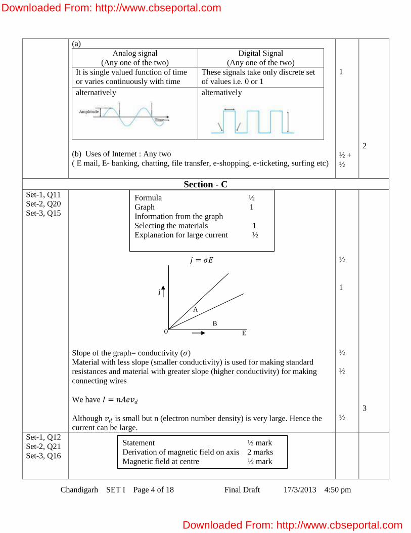
𝑗 = 𝜎𝐸
Slope of the graph= conductivity (𝜎)
Material with less slope (smaller conductivity) is used for making standard
resistances and material with greater slope (higher conductivity) for making
connecting wires
We have 𝐼 = 𝑛𝐴𝑒𝑣𝑑
Although 𝑣𝑑 is small but n (electron number density) is very large. Hence the
current can be large.
½
1
½
½
½
3
Set-1, Q12
Set-2, Q21
Set-3, Q16
Formula ½
Graph 1
Information from the graph
Selecting the materials 1
Explanation for large current ½
Statement ½ mark
Derivation of magnetic field on axis 2 marks
Magnetic field at centre ½ mark
j
o E
B
A
Downloaded From: http://www.cbseportal.com
Downloaded From: http://www.cbseportal.com
Chandigarh SET I Page 5 of 18 Final Draft 17/3/2013 4:50 pm
Biot Savart’s law
𝑑𝐵 ∝ 𝐼 𝑑𝑙 ×𝑟
𝑟3
Or 𝑑𝐵 = 𝜇𝜊
4𝜋 𝐼
𝑑𝑙 ×𝑟
𝑟2
[Also accept if the student writes 𝑑𝐵 ∝ 𝐼, 𝑑𝐵 ∝ 𝑑𝑙 𝑎𝑛𝑑 𝑑𝐵 ∝1
𝑟2 ]
Derivation
The resultant magnetic field will be along the axis as the perpendicular (to the
axis) components cancel out in pairs.
B = ∫𝑜
𝑒𝜋𝑅𝑑𝐵 cos 𝜃
= ∫𝑜
2𝜋𝑅 𝜇0
4𝜋
𝐼𝑑𝑙
(𝑅2+𝑥2)
𝑅
(𝑅2+𝑥2)1/2
= 𝜇0𝐼
4𝜋
2𝜋𝑅2
(𝑅2+𝑥2)3/2 =
𝜇0𝐼𝑅2
2(𝑅2+𝑥2)3/2
At centre, x= 0
∴ 𝐵0 = 𝜇0𝐼
2𝑅
½
½
½
½
½
½
3
Set-1, Q13
Set-2, Q22
Set-3, Q17
Polaroid consists of long chain molecules aligned in a particular direction
Transverse nature of light.
1
Polaroid 1
Transverse nature of light 1
Required Explanation 1
Downloaded From: http://www.cbseportal.com
Downloaded From: http://www.cbseportal.com
Chandigarh SET I Page 6 of 18 Final Draft 17/3/2013 4:50 pm
Alternatively
Explanation:
Unpolarised light incident on a polaroid, gets linearly polarized with electric
vector oscillating along the pass axis of Polaroid.
It will pass out with same intensity from P2, if pass axis of P2 is parallel to that
of P1. On rotating P2 intensity of light reduces to zero when their pass axes are
perpendicular to each other showing transverse nature of light.
Explanation for intensity of light
Unpolarised light incident on a Polaroid, gets polarized and its intensity is
reduced to half and it does not depend on the orientation of the Polaroid.
½
½
½
½
3
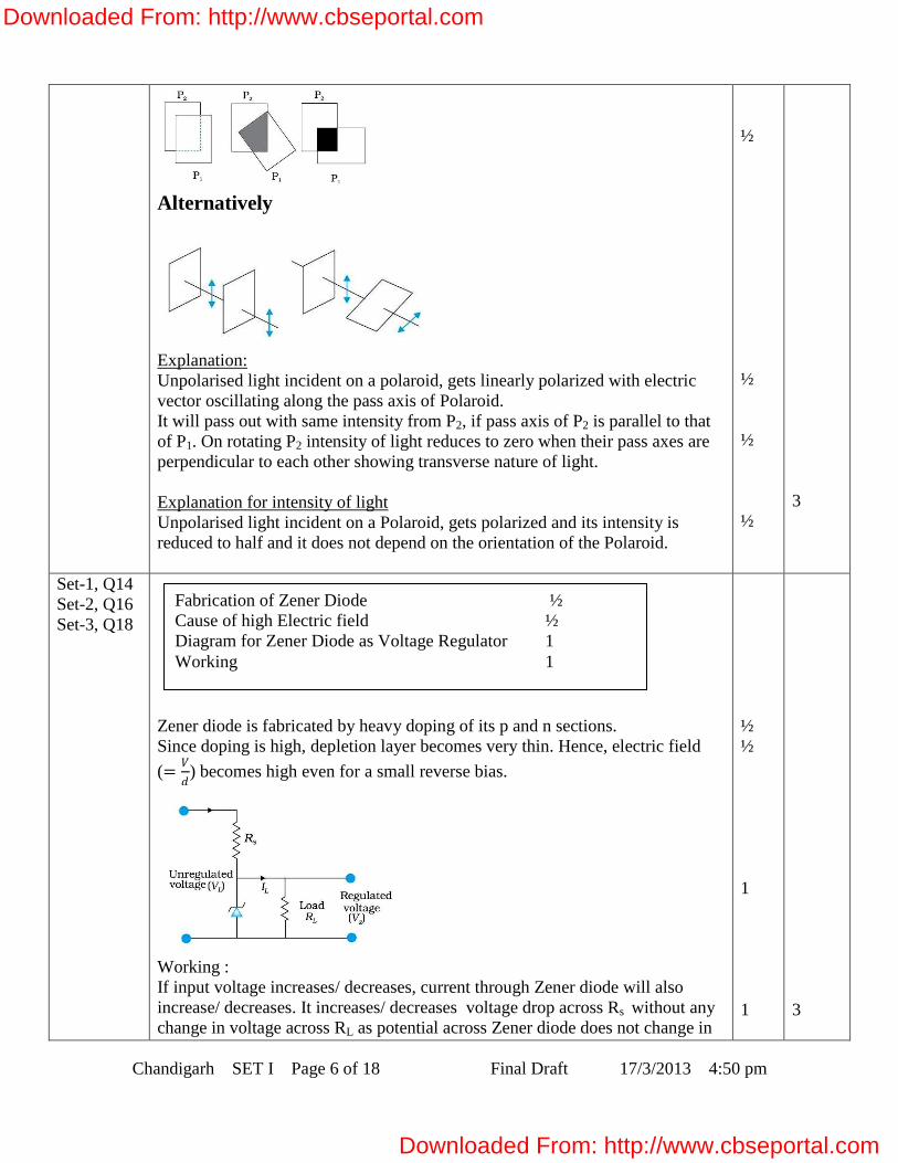
Set-1, Q14
Set-2, Q16
Set-3, Q18
Zener diode is fabricated by heavy doping of its p and n sections.
Since doping is high, depletion layer becomes very thin. Hence, electric field
(=𝑉
𝑑) becomes high even for a small reverse bias.
Working :
If input voltage increases/ decreases, current through Zener diode will also
increase/ decreases. It increases/ decreases voltage drop across Rs without any
change in voltage across RL as potential across Zener diode does not change in
½
½
1
1
3
Fabrication of Zener Diode ½
Cause of high Electric field ½
Diagram for Zener Diode as Voltage Regulator 1
Working 1
Downloaded From: http://www.cbseportal.com
Downloaded From: http://www.cbseportal.com

Chandigarh SET I Page 7 of 18 Final Draft 17/3/2013 4:50 pm
breakdown region giving the regulated output voltage.
OR
a)
Explanation
Due to concentration gradient across p and n sides, holes from p diffuse into n
section and leave behind ionized acceptor (negatively) ions which are
immobile. As holes continue to diffuse from p to n, a layer of negative charge
on p side of junction is formed. Similarly, the diffusion of electrons from n to p
will form a positive charge space region on the n side.
The space charge region on either side of the junction which gets devoid of
mobile charge carrier is known as the depletion layer.
The loss of electrons from n side and holes from p side cause a potential
difference across the junction. This is known as the called barrier potential .
b) Barrier potential decreases in forward bias .
Barrier potential increases in reverse bias.
½
1
½
½
½
3
Set-1, Q15
Set-2, Q17
Set-3, Q11
i) Anode current will increase with increase of intensity
More is intensity of light, more is the number of photons and hence more
number of electrons are emitted
ii) No effect
½
½
½
(a) Diagram ½
Formation of depletion region 1
Potential barrier ½
b) Effect on barrier potential 1
Working – 1 mark
Effect in each case 1½
Justification in each case 1½
Downloaded From: http://www.cbseportal.com
Downloaded From: http://www.cbseportal.com

Chandigarh SET I Page 8 of 18 Final Draft 17/3/2013 4:50 pm
Frequency of light affects the maximum K.E. of the emitted photoelectrons.
iii) Anode current will increase with anode potential
More anode potential will accelerate the electrons more till it attains a
saturation value and get them collected at the anode at a faster rate.
½
½
½
3
Set-1, Q16
Set-2, Q18
Set-3, Q12
Active State :
When the emitter base junction is forward biased and the base collector junction
is reverse biased with 𝑉𝑖 > 0.6𝑉 𝑜𝑟 𝑉𝑖 > 0.3𝑉.
(Also accept any other correct answer)
Diagram :
Explanation :
If 𝑉𝑖 is +ve or –ve , changes in 𝑉𝐵𝐸 will produce changes in 𝐼𝑐 and hence
changes in 𝑉𝐶𝐸 which will appear in amplified form
Base is thin so that there are few majority carriers in it.
Emitter is heavily doped so that it supplies more number of majority charge
carriers.
(Note: Award 1 mark if the student writes the reason for any one case)
½
1
½
½
½
3
Set-1, Q17
Set-2, Q19
Set-3, Q13
Need of Modulation:
1. To have smaller height of antenna [ℎ~𝜆
4]
½
Active state ½
Circuit diagram 1
Working ½
Reasons in each case 1
Factors for need of modulation 1½
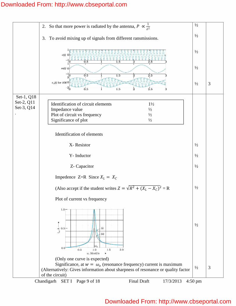
Sketch of carrier wave, modulating wave and AM wave 1½
= 𝑉𝐶𝐸
Downloaded From: http://www.cbseportal.com
Downloaded From: http://www.cbseportal.com
Chandigarh SET I Page 9 of 18 Final Draft 17/3/2013 4:50 pm
2. So that more power is radiated by the antenna, 𝑃 ∝1
𝜆2
3. To avoid mixing up of signals from different ransmissions.
½
½
½
½
½
3
Set-1, Q18
Set-2, Q11
Set-3, Q14
.
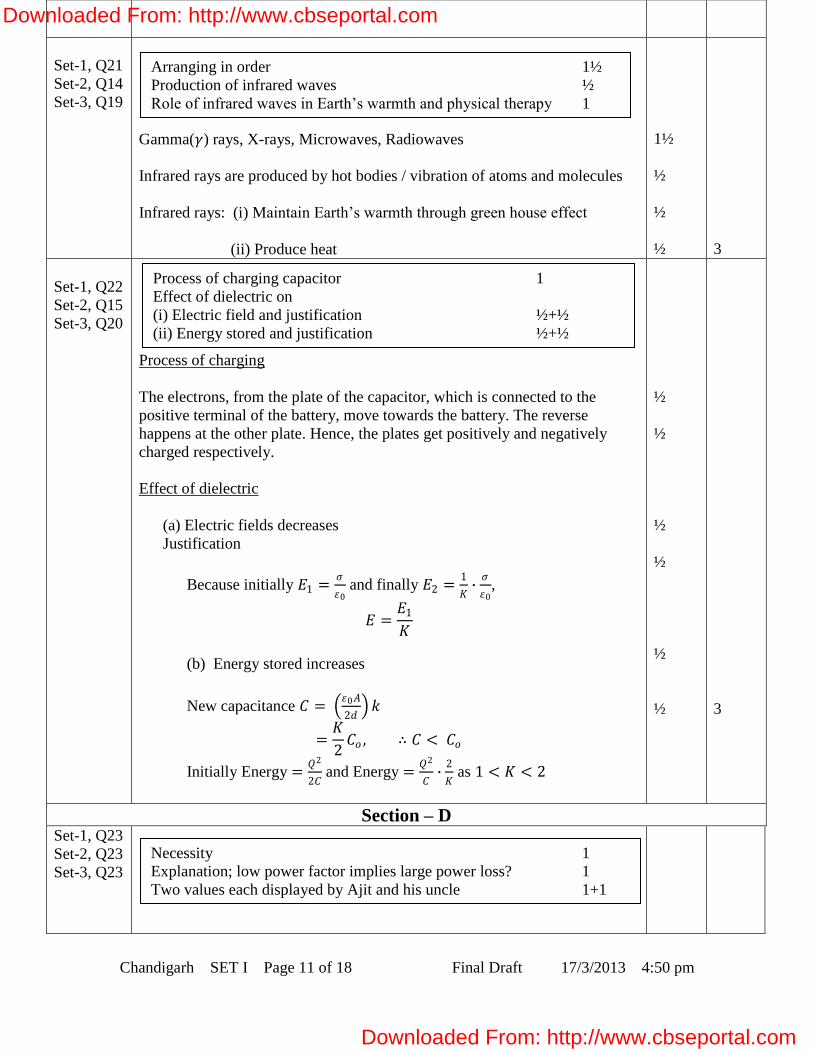
Identification of elements
X- Resistor
Y- Inductor
Z- Capacitor
Impedence Z=R Since 𝑋𝐿 = 𝑋𝐶
(Also accept if the student writes 𝑍 = 𝑅2 + (𝑋𝐿 − 𝑋𝐶)2 = R
Plot of current vs frequency
(Only one curve is expected)
Significance, at 𝑤 = 𝜔𝑜 (resonance frequency) current is maximum
(Alternatively: Gives information about sharpness of resonance or quality factor
of the circuit)
½
½
½
½
½
½
3
Identification of circuit elements 1½
Impedance value ½
Plot of circuit vs frequency ½
Significance of plot ½
Downloaded From: http://www.cbseportal.com
Downloaded From: http://www.cbseportal.com

Chandigarh SET I Page 10 of 18 Final Draft 17/3/2013 4:50 pm
Set-1, Q19
Set-2, Q12
Set-3, Q21
Equation 𝐶611 → 𝑋5
11 + 𝑖𝑒 + 𝑣 + 𝑄
(Also accept if the student does not write 𝑣 𝑜𝑟 𝑄 on the R.H.S.)
X is an isobar
Mass defect (𝛥m) = 𝑚( 𝐶)611 − 𝑚( 𝑋5
11 )
= (11.011434 – 11.009305)u
= 0.002129 u
Q= 𝛥m ×931.5 MeV
= 0.002129 × 931.5 MeV
= 1.98 MeV
1
½
½
½
½
3
Set-1, Q20
Set-2, Q13
Set-3, Q22
1
𝑣+
1
15=
1
10
For lens 1
𝑣−
1
𝑢=
1
𝑓
1
𝑣−
1
−15=
1
+10
∴ 𝑣 = 30 cm
Nature of image- real, magnified
Final image formed will be at the object itself only if image formed by lens is at
the position of centre of curvature of mirror
∴ 𝐷 = 30 + 𝑅 𝑐𝑚 = 30 + 20 𝑐𝑚 = 50 𝑐𝑚 (Distance of mirror from lens)
½
½
½
½
½
½
3
Equation of 𝛽+ decay 1
Identification ½
Calculation of mass defect ½
Calculation of Q value 1
Calculation to find image formed by lens 1½
Nature of image ½
Distance of mirror from lens 1
Downloaded From: http://www.cbseportal.com
Downloaded From: http://www.cbseportal.com
Chandigarh SET I Page 11 of 18 Final Draft 17/3/2013 4:50 pm
Set-1, Q21
Set-2, Q14
Set-3, Q19
Gamma(𝛾) rays, X-rays, Microwaves, Radiowaves
Infrared rays are produced by hot bodies / vibration of atoms and molecules
Infrared rays: (i) Maintain Earth’s warmth through green house effect
(ii) Produce heat
1½
½
½
½
3
Set-1, Q22
Set-2, Q15
Set-3, Q20
𝐸 =𝐸1
𝐾
=𝐾
2𝐶𝑜 , ∴ 𝐶 < 𝐶𝑜
Process of charging
The electrons, from the plate of the capacitor, which is connected to the
positive terminal of the battery, move towards the battery. The reverse
happens at the other plate. Hence, the plates get positively and negatively
charged respectively.
Effect of dielectric
(a) Electric fields decreases
Justification
Because initially 𝐸1 =𝜎
𝜀0 and finally 𝐸2 =
1
𝐾∙
𝜎
𝜀0,
(b) Energy stored increases
New capacitance 𝐶 = 𝜀0𝐴
2𝑑 𝑘
Initially Energy =𝑄2
2𝐶 and Energy =
𝑄2
𝐶∙
2
𝐾 as 1 < 𝐾 < 2
½
½
½
½
½
½
3
Section – D
Set-1, Q23
Set-2, Q23
Set-3, Q23
Arranging in order 1½
Production of infrared waves ½
Role of infrared waves in Earth’s warmth and physical therapy 1
Process of charging capacitor 1
Effect of dielectric on
(i) Electric field and justification ½+½
(ii) Energy stored and justification ½+½
Necessity 1
Explanation; low power factor implies large power loss? 1
Two values each displayed by Ajit and his uncle 1+1
Downloaded From: http://www.cbseportal.com
Downloaded From: http://www.cbseportal.com
Chandigarh SET I Page 12 of 18 Final Draft 17/3/2013 4:50 pm
a) For the same power at high voltage, current in the transmission wires
becomes smaller.
∴ power loss is less
[Award ½ mark if the student just writes 𝑃 = 𝐼2𝑅]
b) If power factor is less, current in the cables is more so power loss is
more
[Alternately 𝑃𝑎𝑣 = 𝐸𝑣𝐼𝑣 cos 𝜃
If cos 𝜃is less, 𝐼𝑣 is more so power loss is more]
(Award ½ mark if the student just writes 𝑃 = 𝐸𝐸𝐼𝑣 cos 𝜃
c) Values displayed
By Ajit (Any two) – Social Awareness, understanding nature, concern
for society
By Uncle- Knowledgeable, professional honesty, concern for society.
(Also accept other suitable values)
½
½
1
½ +½
½ +½
4
Section - E
Set-1, Q24
Set-2, Q26
Set-3, Q25
a) Self inductance of a coil is numerically equal to magnetic flux linked
with the coil when unit current passes through it. 𝐿 =𝜑
𝐼
Alternately
Self inductance of a coil is numerically equal to induced e.m.f.
produced in it when rate of change of current is unity in it.
Expression for energy
Induced e.m.f. produced in coil, 𝜀 = −𝐿𝑑𝐼
𝑑𝑡
∴ work done by the source, dw= +𝜀𝐼𝑑𝑡 = 𝐿𝐼𝑑𝐼
𝑊 = ∫ 𝐿𝐼𝑑𝐼 = 1
2
𝐼
𝑂𝐿𝐼2
b) Direction of induced current – clockwise (MNOP)
[A student can also show the direction in the diagram itself]
Duration of induced current - 1s
1
½
½
½+½
½
½
Definition of self-inductance 1
Expression for energy stored 2
Direction of induced current ½
Duration of induced current ½
Graphs of magnetic flux and induced e.m.f 1
Downloaded From: http://www.cbseportal.com
Downloaded From: http://www.cbseportal.com
Chandigarh SET I Page 13 of 18 Final Draft 17/3/2013 4:50 pm
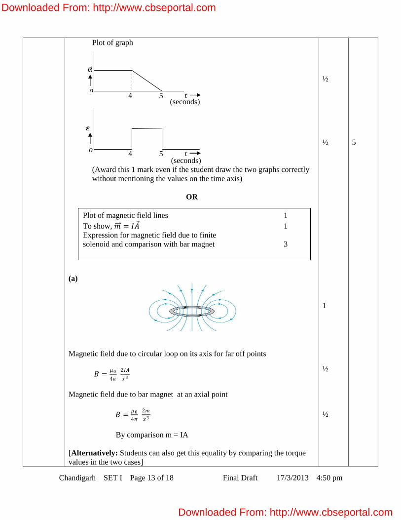
Plot of graph
(Award this 1 mark even if the student draw the two graphs correctly
without mentioning the values on the time axis)
OR
(a)
Magnetic field due to circular loop on its axis for far off points
𝐵 =𝜇0
4𝜋
2𝐼𝐴
𝑥3
Magnetic field due to bar magnet at an axial point
𝐵 =𝜇0
4𝜋
2𝑚
𝑥3
By comparison m = IA
[Alternatively: Students can also get this equality by comparing the torque
values in the two cases]
½
½
1
½
½
5
∅
4 5 𝑡 𝑜
𝜺
𝑜 𝑡 5 4
Plot of magnetic field lines 1
To show, 𝑚 = 𝐼𝐴 1
Expression for magnetic field due to finite
solenoid and comparison with bar magnet 3
(seconds)
(seconds)
Downloaded From: http://www.cbseportal.com
Downloaded From: http://www.cbseportal.com

Chandigarh SET I Page 14 of 18 Final Draft 17/3/2013 4:50 pm
∴ 𝐵 = 𝜇0𝐼𝑎
2𝑛
2 × 𝑟3 𝑑𝑥
+𝑙
−𝑙
= 𝜇0𝑛𝐼
2 2𝑙𝑎2
𝑟3
a) Magnetic field on the axis of a finite solenoid
Magnetic field due to element dx at point P
𝑑𝐵 = 𝜇0𝑛𝑑𝑥𝐼 𝑎2
2[(𝑟−𝑥)2+ 𝑎2]3
2
For r >> 𝑎, ( r >> 𝑙)
Magnetic moment of solenoid, 𝑚 = 𝑛 × 2𝑙 𝐼(𝜋𝑎2)
∴ 𝐵 =𝜇𝑜
4𝜋 2𝑚
𝑟3 same as that of a bar magnet
1
½
½
½
½
5
Set-1, Q25
Set-2, Q24
Set-3, Q26
Diagram
½
Conditions for constructive and destructive interference 1½
Expression for fringe width 2
Fringe pattern in double slit related to diffraction pattern ½
Numerical 1
𝜃
∴ 𝐵 = 𝑑𝐵 =𝜇0𝐼𝑎
2 × 𝑛
2
𝑑𝑥
[(𝑟 − 𝑥)2 + 𝑎2]3/2
+𝑙
−𝑙
Downloaded From: http://www.cbseportal.com
Downloaded From: http://www.cbseportal.com
Chandigarh SET I Page 15 of 18 Final Draft 17/3/2013 4:50 pm
(a) Path difference (∆) = 𝑆2𝑃 − 𝑆1𝑃 = 𝑑 sin 𝜃 =𝑑𝑥
𝐷
For constructive interference, ∆= 𝑛𝜆 [𝑛 = 0,1,2. . ]
Destructive interference, ∆= 2𝑛 − 1 𝜆
2[𝑛 = 1,2. . ]
For bright bands, ∆= 𝑛𝜆 =𝑥𝑛𝑑
𝐷 𝑜𝑟 𝑥𝑛 =
𝑛𝜆𝐷
𝑑
For dark bands, ∆= 2𝑛 − 1 𝜆
2=
𝑥𝑛𝑑
𝐷 𝑜𝑟 𝑥𝑛 = 2𝑛 − 1
𝜆𝐷
2𝑑
Fringe width 𝛽 = 𝑋𝑛 − 𝑋𝑛−1 = 𝜆𝐷
𝑑
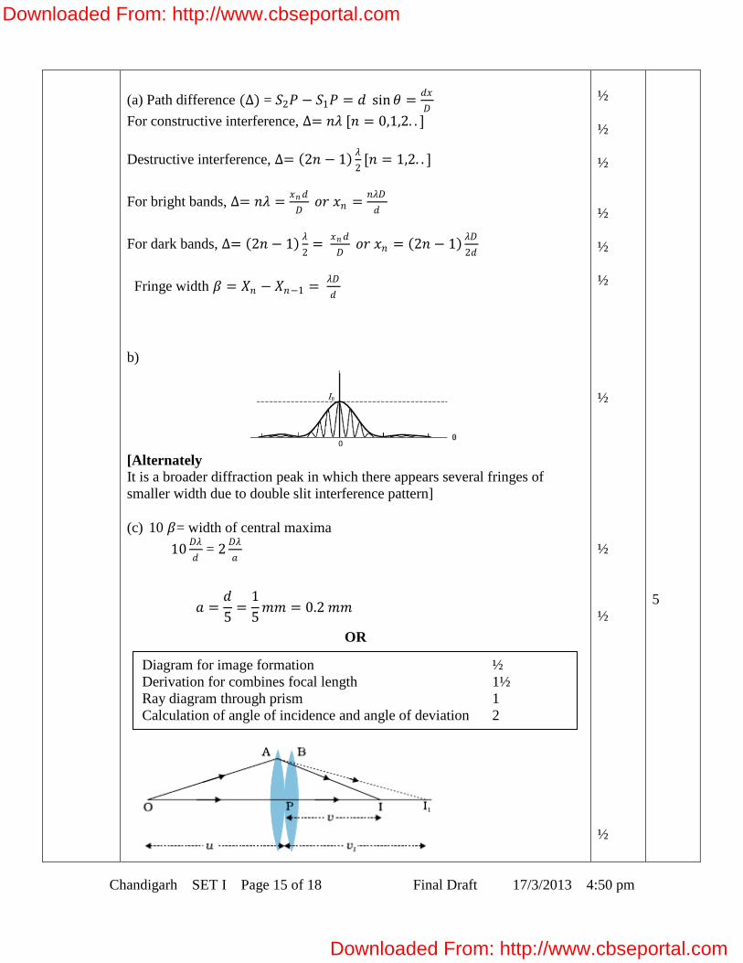
b)
[Alternately
It is a broader diffraction peak in which there appears several fringes of
smaller width due to double slit interference pattern]
(c) 10 𝛽= width of central maxima
10𝐷𝜆
𝑑 = 2
𝐷𝜆
𝑎
OR
½
½
½
½
½
½
½
½
½
½
5
𝑎 =𝑑
5=
1
5𝑚𝑚 = 0.2 𝑚𝑚
Diagram for image formation ½
Derivation for combines focal length 1½
Ray diagram through prism 1
Calculation of angle of incidence and angle of deviation 2
Downloaded From: http://www.cbseportal.com
Downloaded From: http://www.cbseportal.com
Chandigarh SET I Page 16 of 18 Final Draft 17/3/2013 4:50 pm
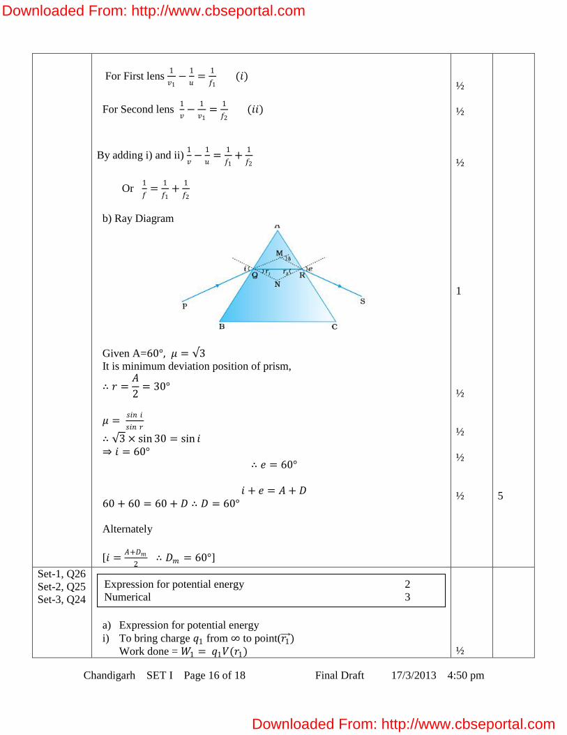
∴ 𝑟 =𝐴
2= 30°
∴ 3 × sin 30 = sin 𝑖 ⇒ 𝑖 = 60°
∴ 𝑒 = 60°
𝑖 + 𝑒 = 𝐴 + 𝐷
For First lens 1
𝑣1−
1
𝑢=
1
𝑓1 (𝑖)
For Second lens 1
𝑣−
1
𝑣1=
1
𝑓2 (𝑖𝑖)
By adding i) and ii) 1
𝑣−
1
𝑢=
1
𝑓1+
1
𝑓2
Or 1
𝑓=
1
𝑓1+
1
𝑓2
b) Ray Diagram
Given A=60°, 𝜇 = 3
It is minimum deviation position of prism,
𝜇 = 𝑠𝑖𝑛 𝑖
𝑠𝑖𝑛 𝑟
60 + 60 = 60 + 𝐷 ∴ 𝐷 = 60°
Alternately
[𝑖 =𝐴+𝐷𝑚
2 ∴ 𝐷𝑚 = 60°]
½
½
½
1
½
½
½
½
5
Set-1, Q26
Set-2, Q25
Set-3, Q24
a) Expression for potential energy
i) To bring charge 𝑞1 from ∞ to point(𝑟1 )
Work done = 𝑊1 = 𝑞1𝑉(𝑟1)
½
Expression for potential energy 2
Numerical 3
Downloaded From: http://www.cbseportal.com
Downloaded From: http://www.cbseportal.com
Chandigarh SET I Page 17 of 18 Final Draft 17/3/2013 4:50 pm
ii) To bring charge 𝑞2 from ∞ to point(𝑟2 )
Work done = 𝑊2 = 𝑞2𝑉(𝑟2) +1
4𝜋𝜀𝑜∙
𝑞1𝑞2
𝑟12
∴ Potential energy 𝑈 = 𝑊1 + 𝑊2 = 𝑞1𝑉 𝑟1 + 𝑞2𝑉 𝑟2 +𝐾𝑞1𝑞2
𝑟12
b) 𝑈𝑖 =1
4𝜋𝜀𝑜 𝑄×2𝑄
𝑙+
𝑄 −3 𝑄
𝑙+
2𝑄× −3 𝑄
𝑙
= - 1
4𝜋𝜀𝑜
7𝑄2
𝑙
𝑊 = 𝑈𝑓 − 𝑈𝑖 =- 1
4𝜋𝜀𝑜
7𝑄2
𝑙
(If a student writes 𝑈𝑖 =1
4𝜋𝜀𝑜
𝑞𝑖𝑞𝑗
𝑟𝑖𝑗 , award ½ mark)
Or
Electric flux through a given area is defined as the number of electric field
lines crossing normally through that area
[Alternately,
Electric flux is the surface integral of electric field over the surface
S.I. unit - 𝑁𝑚2𝐶−1 𝑜𝑟 𝑉𝑚
Gauss Law: Electric flux through a given closed surface is 1
𝜀𝑜 times the
charge enclosed by the closed surface
Flux of a point charge placed at the centre of cube = 𝑞
𝜀𝑜
½
1
1
1
1
1
½
1½
1
5
𝑈𝑓 =1
4𝜋𝜀𝑜 𝑄 × 2𝑄
𝑙2
+𝑄 −3 𝑄
𝑙2
+2𝑄 × −3 𝑄
𝑙2
= - 1
4𝜋𝜀𝑜
14𝑄2
𝑙
Definition of electric flux 1
S.I. unit ½
State and explain Gauss’s law 1½
Outward flux 1
Flux is independent of shape and size 1
Φ = 𝐸 . 𝑑𝑠 ]
[𝐴𝑙𝑡𝑒𝑟𝑛𝑎𝑡𝑖𝑣𝑒𝑙𝑦: 𝜙 =𝑞
𝜀𝑜]
Downloaded From: http://www.cbseportal.com
Downloaded From: http://www.cbseportal.com

Chandigarh SET I Page 18 of 18 Final Draft 17/3/2013 4:50 pm
As the Electric field is radial and inversely proportional to the square of
distnce. Therefore, it is independent of shape and size. The number of
electric field lines, crossing normally through a closed surface depends only
on the charge enclosed by it.
1
5
Downloaded From: http://www.cbseportal.com
Downloaded From: http://www.cbseportal.com