pic18f2480/2580/4480/4580 data sheetpic18f2480/2580/4480/4580 data sheet ... 3, +-
TRANSCRIPT

© 2009 Microchip Technology Inc. DS39637D
PIC18F2480/2580/4480/4580Data Sheet
28/40/44-PinEnhanced Flash Microcontrollers
with ECAN™ Technology, 10-Bit A/Dand nanoWatt Technology

Note the following details of the code protection feature on Microchip devices:• Microchip products meet the specification contained in their particular Microchip Data Sheet.
• Microchip believes that its family of products is one of the most secure families of its kind on the market today, when used in the intended manner and under normal conditions.
• There are dishonest and possibly illegal methods used to breach the code protection feature. All of these methods, to our knowledge, require using the Microchip products in a manner outside the operating specifications contained in Microchip’s Data Sheets. Most likely, the person doing so is engaged in theft of intellectual property.
• Microchip is willing to work with the customer who is concerned about the integrity of their code.
• Neither Microchip nor any other semiconductor manufacturer can guarantee the security of their code. Code protection does not mean that we are guaranteeing the product as “unbreakable.”
Code protection is constantly evolving. We at Microchip are committed to continuously improving the code protection features of ourproducts. Attempts to break Microchip’s code protection feature may be a violation of the Digital Millennium Copyright Act. If such actsallow unauthorized access to your software or other copyrighted work, you may have a right to sue for relief under that Act.
Information contained in this publication regarding deviceapplications and the like is provided only for your convenienceand may be superseded by updates. It is your responsibility toensure that your application meets with your specifications.MICROCHIP MAKES NO REPRESENTATIONS ORWARRANTIES OF ANY KIND WHETHER EXPRESS ORIMPLIED, WRITTEN OR ORAL, STATUTORY OROTHERWISE, RELATED TO THE INFORMATION,INCLUDING BUT NOT LIMITED TO ITS CONDITION,QUALITY, PERFORMANCE, MERCHANTABILITY ORFITNESS FOR PURPOSE. Microchip disclaims all liabilityarising from this information and its use. Use of Microchipdevices in life support and/or safety applications is entirely atthe buyer’s risk, and the buyer agrees to defend, indemnify andhold harmless Microchip from any and all damages, claims,suits, or expenses resulting from such use. No licenses areconveyed, implicitly or otherwise, under any Microchipintellectual property rights.
DS39637D-page 2
Trademarks
The Microchip name and logo, the Microchip logo, dsPIC, KEELOQ, KEELOQ logo, MPLAB, PIC, PICmicro, PICSTART, rfPIC and UNI/O are registered trademarks of Microchip Technology Incorporated in the U.S.A. and other countries.
FilterLab, Hampshire, HI-TECH C, Linear Active Thermistor, MXDEV, MXLAB, SEEVAL and The Embedded Control Solutions Company are registered trademarks of Microchip Technology Incorporated in the U.S.A.
Analog-for-the-Digital Age, Application Maestro, CodeGuard, dsPICDEM, dsPICDEM.net, dsPICworks, dsSPEAK, ECAN, ECONOMONITOR, FanSense, HI-TIDE, In-Circuit Serial Programming, ICSP, Mindi, MiWi, MPASM, MPLAB Certified logo, MPLIB, MPLINK, mTouch, Octopus, Omniscient Code Generation, PICC, PICC-18, PICDEM, PICDEM.net, PICkit, PICtail, PIC32 logo, REAL ICE, rfLAB, Select Mode, Total Endurance, TSHARC, UniWinDriver, WiperLock and ZENA are trademarks of Microchip Technology Incorporated in the U.S.A. and other countries.
SQTP is a service mark of Microchip Technology Incorporated in the U.S.A.
All other trademarks mentioned herein are property of their respective companies.
© 2009, Microchip Technology Incorporated, Printed in the U.S.A., All Rights Reserved.
Printed on recycled paper.
© 2009 Microchip Technology Inc.
Microchip received ISO/TS-16949:2002 certification for its worldwide headquarters, design and wafer fabrication facilities in Chandler and Tempe, Arizona; Gresham, Oregon and design centers in California and India. The Company’s quality system processes and procedures are for its PIC® MCUs and dsPIC® DSCs, KEELOQ® code hopping devices, Serial EEPROMs, microperipherals, nonvolatile memory and analog products. In addition, Microchip’s quality system for the design and manufacture of development systems is ISO 9001:2000 certified.

PIC18F2480/2580/4480/458028/40/44-Pin Enhanced Flash Microcontrollers with
ECAN™ Technology, 10-Bit A/D and nanoWatt Technology
Power-Managed Modes:• Run: CPU on, Peripherals on• Idle: CPU off, Peripherals on• Sleep: CPU off, Peripherals off• Idle mode Currents Down to 6.1 μA Typical• Sleep mode Current Down to 0.2 μA Typical• Timer1 Oscillator: 1 μA, 32 kHz, 2V• Watchdog Timer: 1.7 μA• Two-Speed Oscillator Start-up
Flexible Oscillator Structure:• Four Crystal modes, up to 40 MHz• 4x Phase Lock Loop (PLL) – Available for Crystal
and Internal Oscillators)• Two External RC modes, up to 4 MHz• Two External Clock modes, up to 40 MHz• Internal Oscillator Block:
- Fast wake from Sleep and Idle, 1 μs typical- 8 user-selectable frequencies, from 31 kHz to 8 MHz- Provides a complete range of clock speeds,
from 31 kHz to 32 MHz when used with PLL- User-tunable to compensate for frequency drift
• Secondary Oscillator using Timer1 @ 32 kHz• Fail-Safe Clock Monitor
- Allows for safe shutdown if peripheral clock stops
Special Microcontroller Features:• C Compiler Optimized Architecture with Optional
Extended Instruction Set• 100,000 Erase/Write Cycle Enhanced Flash
Program Memory Typical• 1,000,000 Erase/Write Cycle Data EEPROM
Memory Typical• Flash/Data EEPROM Retention: > 40 Years• Self-Programmable under Software Control• Priority Levels for Interrupts• 8 x 8 Single-Cycle Hardware Multiplier• Extended Watchdog Timer (WDT):
- Programmable period from 41 ms to 131s• Single-Supply 5V In-Circuit Serial
Programming™ (ICSP™) via Two Pins• In-Circuit Debug (ICD) via Two Pins• Wide Operating Voltage Range: 2.0V to 5.5V
Peripheral Highlights:• High-Current Sink/Source 25 mA/25 mA• Three External Interrupts• One Capture/Compare/PWM (CCP) module• Enhanced Capture/Compare/PWM (ECCP) module
(40/44-pin devices only):- One, two or four PWM outputs- Selectable polarity- Programmable dead time- Auto-shutdown and auto-restart
• Master Synchronous Serial Port (MSSP) module Supporting 3-Wire SPI (all 4 modes) and I2C™ Master and Slave modes
• Enhanced Addressable USART module- Supports RS-485, RS-232 and LIN/J2602- RS-232 operation using internal oscillator
block- Auto-wake-up on Start bit- Auto-Baud Detect
• 10-Bit, up to 11-Channel Analog-to-Digital Converter (A/D) module, up to 100 ksps- Auto-acquisition capability- Conversion available during Sleep
• Dual Analog Comparators with Input Multiplexing
ECAN Technology Module Features:• Message Bit Rates up to 1 Mbps• Conforms to CAN 2.0B Active Specification• Fully Backward Compatible with PIC18XXX8 CAN
modules• Three Modes of Operation:
- Legacy, Enhanced Legacy, FIFO• Three Dedicated Transmit Buffers with Prioritization• Two Dedicated Receive Buffers• Six Programmable Receive/Transmit Buffers• Three Full 29-Bit Acceptance Masks• 16 Full 29-Bit Acceptance Filters w/Dynamic
Association• DeviceNet™ Data Byte Filter Support• Automatic Remote Frame Handling• Advanced Error Management Features
DeviceProgram Memory Data Memory
I/O 10-BitA/D (ch)
CCP/ECCP(PWM)
MSSP
EUSA
RT
Comp. Timers8/16-bitFlash
(bytes)# Single-WordInstructions
SRAM(bytes)
EEPROM(bytes) SPI Master
I2C™
PIC18F2480 16K 8192 768 256 25 8 1/0 Y Y 1 0 1/3PIC18F2580 32K 16384 1536 256 25 8 1/0 Y Y 1 0 1/3PIC18F4480 16K 8192 768 256 36 11 1/1 Y Y 1 2 1/3PIC18F4580 32K 16384 1536 256 36 11 1/1 Y Y 1 2 1/3
© 2009 Microchip Technology Inc. DS39637D-page 3

PIC18F2480/2580/4480/4580
Pin DiagramsRB7/KBI3/PGDRB6/KBI2/PGCRB5/KBI1/PGMRB4/KBI0/AN9RB3/CANRXRB2/INT2/CANTXRB1/INT1/AN8RB0/INT0/FLT0/AN10VDDVSS
RD7/PSP7/P1DRD6/PSP6/P1CRD5/PSP5/P1BRD4/PSP4/ECCP1/P1ARC7/RX/DTRC6/TX/CKRC5/SDORC4/SDI/SDARD3/PSP3/C2IN-RD2/PSP2/C2IN+
MCLR/VPP/RE3RA0/AN0/CVREF
RA1/AN1RA2/AN2/VREF-RA3/AN3/VREF+
RA4/T0CKIRA5/AN4/SS/HLVDIN
RE0/RD/AN5RE1/WR/AN6/C1OUTRE2/CS/AN7/C2OUT
VDDVSS
OSC1/CLKI/RA7OSC2/CLKO/RA6
RC0/T1OSO/T13CKIRC1/T1OSIRC2/CCP1
RC3/SCK/SCLRD0/PSP0/C1IN+RD1/PSP1/C1IN-
1234567891011121314151617181920
4039383736353433323130292827262524232221
PIC
18F4
480
40-Pin PDIP
PIC
18F4
580
PIC
18F2
480
1011
23456
1
87
9
121314 15
1617181920
232425262728
2221
MCLR/VPP/RE3RA0/AN0RA1/AN1
RA2/AN2/VREF-RA3/AN3/VREF+
RA4/T0CKIRA5/AN4/SS/HLVDIN
VSS
OSC1/CLKI/RA7OSC2/CLKO/RA6
RC0/T1OSO/T13CKIRC1/T1OSIRC2/CCP1
RC3/SCK/SCL
RB7/KBI3/PGDRB6/KBI2/PGCRB5/KBI1/PGMRB4/KBI0/AN9RB3/CANRXRB2/INT2/CANTXRB1/INT1/AN8RB0/INT0/AN10VDD
VSS
RC7/RX/DTRC6/TX/CKRC5/SDORC4/SDI/SDA
28-Pin SPDIP, SOIC
PIC
18F2
580
28-Pin QFN
10 11
23
6
1
18192021
22
12 13 1415
87
1617
232425262728
9
PIC18F2480
RC
0/T1
OSO
/T13
CK
I
54
RB
7/K
BI3/
PG
DR
B6/
KBI
2/P
GC
RB
5/K
BI1/
PG
MR
B4/
KBI
0/A
N9
RB3/CANRXRB2/INT2/CANTXRB1/INT1/AN8RB0/INT0/AN10VDDVSSRC7/RX/DT
RC
6/TX
/CK
RC
5/S
DO
RC
4/S
DI/S
DA
MC
LR/V
PP/R
E3
RA
0/A
N0
RA
1/A
N1
RA2/AN2/VREF-RA3/AN3/VREF+
RA4/T0CKIRA5/AN4/SS/HLVDIN
VSSOSC1/CLKI/RA7
OSC2/CLKO/RA6
RC
1/T1
OS
IR
C2/
CC
P1
RC
3/S
CK
/SC
L
PIC18F2580
DS39637D-page 4 © 2009 Microchip Technology Inc.

PIC18F2480/2580/4480/4580
Pin Diagrams (Continued)1011
23
6
1
18 19 20 21 2212 13 14 15
38
87
44 43 42 41 40 3916 17
2930313233
232425262728
36 3435
9
PIC18F4480
37
RA
3/A
N3/
VRE
F+R
A2/A
N2/
V RE
F-R
A1/
AN
1R
A0/
AN
0/C
V RE
FM
CLR
/VP
P/R
E3NC
RB
7/K
BI3
/PG
DR
B6/
KB
I2/P
GC
RB
5/KB
I1/P
GM
RB4
/KB
I0/A
N9
NC
RC
6/TX
/CK
RC
5/S
DO
RC
4/S
DI/S
DA
RD
3/P
SP3
/C2I
N-
RD
2/P
SP2
/C2I
N+
RD
1/P
SP1
/C1I
N-
RD
0/P
SP0
/C1I
N+
RC
3/S
CK
/SC
LR
C2/
CC
P1
RC
1/T1
OS
IN
C
NCRC0/T1OSO/T13CKIOSC2/CLKO/RA6OSC1/CLKI/RA7
VSSVDD
RE2/CS/AN7/C2OUTRE1/WR/AN6/C1OUTRE0/RD/AN5RA5/AN4/SS/HLVDINRA4/T0CKI
RC7/RX/DTRD4/PSP4/ECCP1/P1A
RD5/PSP5/P1BRD6/PSP6/P1C
VSSVDD
RB0/INT0/FLT0/AN10RB1/INT1/AN8
RB2/INT2/CANTXRB3/CANRX
44-Pin TQFP
RD7/PSP7/P1D 54
44-Pin QFN(1)
1011
23
6
1
18 19 20 21 2212 13 14 15
38
87
44 43 42 41 40 3916 17
2930313233
232425262728
36 3435
9
PIC18F4480
37
RA
3/A
N3/
VRE
F+R
A2/
AN2/
V RE
F-R
A1/A
N1
RA
0/A
N0/
CVR
EF
MC
LR/V
PP/R
E3
RB
7/KB
I3/P
GD
RB
6/KB
I2/P
GC
RB
5/K
BI1
/PG
MR
B4/
KBI0
/AN
9N
CR
C6/
TX/C
KR
C5/
SD
OR
C4/
SD
I/SD
AR
D3/
PS
P3/
C2I
N-
RD
2/P
SP
2/C
2IN
+R
D1/
PS
P1/
C1I
N-
RD
0/P
SP
0/C
1IN
+R
C3/
SC
K/S
CL
RC
2/C
CP
1R
C1/
T1O
SI
RC
0/T1
OS
O/T
13C
KI
OSC2/CLKO/RA6OSC1/CLKI/RA7VSS
AVDDRE2/CS/AN7/C2OUTRE1/WR/AN6/C1OUTRE0/RD/AN5RA5/AN4/SS/HLVDINRA4/T0CKI
RC7/RX/DT
RD5/PSP5/P1BRD6/PSP6/P1C
VSS
VDDRB0/INT0/FLT0/AN10
RB1/INT1/AN8RB2/INT2/CANTX
RB
3/C
AN
RX
RD7/PSP7/P1D 54 AVSS
VDD
AVDD
PIC18F4580
PIC18F4580
RD4/PSP4/ECCP1/P1A
Note 1: For the QFN package, it is recommended that the bottom pad be connected to VSS.
© 2009 Microchip Technology Inc. DS39637D-page 5

PIC18F2480/2580/4480/4580
Table of Contents1.0 Device Overview .......................................................................................................................................................................... 92.0 Guidelines for Getting Started with PIC18F Microcontrollers ..................................................................................................... 253.0 Oscillator Configurations ............................................................................................................................................................ 294.0 Power-Managed Modes ............................................................................................................................................................. 395.0 Reset .......................................................................................................................................................................................... 476.0 Memory Organization ................................................................................................................................................................. 677.0 Flash Program Memory............................................................................................................................................................ 1018.0 Data EEPROM Memory ........................................................................................................................................................... 1119.0 8 x 8 Hardware Multiplier.......................................................................................................................................................... 11710.0 Interrupts .................................................................................................................................................................................. 11911.0 I/O Ports ................................................................................................................................................................................... 13512.0 Timer0 Module ......................................................................................................................................................................... 15113.0 Timer1 Module ......................................................................................................................................................................... 15514.0 Timer2 Module ......................................................................................................................................................................... 16115.0 Timer3 Module ......................................................................................................................................................................... 16316.0 Capture/Compare/PWM (CCP) Modules ................................................................................................................................. 16717.0 Enhanced Capture/Compare/PWM (ECCP) Module................................................................................................................ 17718.0 Master Synchronous Serial Port (MSSP) Module .................................................................................................................... 19119.0 Enhanced Universal Synchronous Receiver Transmitter (EUSART) ....................................................................................... 23120.0 10-Bit Analog-to-Digital Converter (A/D) Module ..................................................................................................................... 25321.0 Comparator Module.................................................................................................................................................................. 26322.0 Comparator Voltage Reference Module................................................................................................................................... 26923.0 High/Low-Voltage Detect (HLVD)............................................................................................................................................. 27324.0 ECAN Module........................................................................................................................................................................... 27925.0 Special Features of the CPU.................................................................................................................................................... 34926.0 Instruction Set Summary .......................................................................................................................................................... 36727.0 Development Support............................................................................................................................................................... 41728.0 Electrical Characteristics .......................................................................................................................................................... 42129.0 Packaging Information.............................................................................................................................................................. 459Appendix A: Revision History............................................................................................................................................................. 471Appendix B: Device Differences......................................................................................................................................................... 471Appendix C: Conversion Considerations ........................................................................................................................................... 472Appendix D: Migration from Baseline to Enhanced Devices.............................................................................................................. 472Appendix E: Migration From Mid-Range to Enhanced Devices ......................................................................................................... 473Appendix F: Migration From High-End to Enhanced Devices............................................................................................................ 473The Microchip Web Site ..................................................................................................................................................................... 487Customer Change Notification Service .............................................................................................................................................. 487Customer Support .............................................................................................................................................................................. 487Reader Response .............................................................................................................................................................................. 488PIC18F2480/2580/4480/4580 Product Identification System ............................................................................................................ 489DS39637D-page 6 © 2009 Microchip Technology Inc.
PIC18F2480/2580/4480/4580
TO OUR VALUED CUSTOMERSIt is our intention to provide our valued customers with the best documentation possible to ensure successful use of your Microchipproducts. To this end, we will continue to improve our publications to better suit your needs. Our publications will be refined andenhanced as new volumes and updates are introduced. If you have any questions or comments regarding this publication, please contact the Marketing Communications Department viaE-mail at [email protected] or fax the Reader Response Form in the back of this data sheet to (480) 792-4150.We welcome your feedback.
Most Current Data SheetTo obtain the most up-to-date version of this data sheet, please register at our Worldwide Web site at:
http://www.microchip.comYou can determine the version of a data sheet by examining its literature number found on the bottom outside corner of any page.The last character of the literature number is the version number, (e.g., DS30000A is version A of document DS30000).
ErrataAn errata sheet, describing minor operational differences from the data sheet and recommended workarounds, may exist for currentdevices. As device/documentation issues become known to us, we will publish an errata sheet. The errata will specify the revisionof silicon and revision of document to which it applies.To determine if an errata sheet exists for a particular device, please check with one of the following:• Microchip’s Worldwide Web site; http://www.microchip.com• Your local Microchip sales office (see last page)• The Microchip Corporate Literature Center; U.S. FAX: (480) 792-7277When contacting a sales office or the literature center, please specify which device, revision of silicon and data sheet (includeliterature number) you are using.
Customer Notification SystemRegister on our web site at www.microchip.com/cn to receive the most current information on all of our products.
© 2009 Microchip Technology Inc. DS39637D-page 7

PIC18F2480/2580/4480/4580
NOTES:DS39637D-page 8 © 2009 Microchip Technology Inc.

PIC18F2480/2580/4480/4580
1.0 DEVICE OVERVIEWThis document contains device specific information forthe following devices:
• PIC18F2480• PIC18F2580• PIC18F4480• PIC18F4580
This family of devices offers the advantages of allPIC18 microcontrollers – namely, high computationalperformance at an economical price – with the additionof high-endurance, Enhanced Flash programmemory. In addition to these features, thePIC18F2480/2580/4480/4580 family introduces designenhancements that make these microcontrollers alogical choice for many high-performance,power-sensitive applications.
1.1 New Core Features
1.1.1 nanoWatt TECHNOLOGYAll of the devices in the PIC18F2480/2580/4480/4580family incorporate a range of features that can signifi-cantly reduce power consumption during operation.Key items include:
• Alternate Run Modes: By clocking the controller from the Timer1 source or the internal oscillator block, power consumption during code execution can be reduced by as much as 90%.
• Multiple Idle Modes: The controller can also run with its CPU core disabled but the peripherals still active. In these states, power consumption can be reduced even further, to as little as 4% of normal operation requirements.
• On-the-Fly Mode Switching: The power-managed modes are invoked by user code during operation, allowing the user to incorporate power-saving ideas into their application’s software design.
• Lower Consumption in Key Modules: The power requirements for both Timer1 and the Watchdog Timer have been reduced by up to 80%, with typical values of 1.1 and 2.1 μA, respectively.
• Extended Instruction Set: In addition to the standard 75 instructions of the PIC18 instruction set, PIC18F2480/2580/4480/4580 devices also provide an optional extension to the core CPU functionality. The added features include eight additional instructions that augment indirect and indexed addressing operations and the implementation of Indexed Literal Offset Addressing mode for many of the standard PIC18 instructions.
1.1.2 MULTIPLE OSCILLATOR OPTIONS AND FEATURES
All of the devices in the PIC18F2480/2580/4480/4580family offer ten different oscillator options, allowingusers a wide range of choices in developing applicationhardware. These include:
• Four Crystal modes, using crystals or ceramic resonators
• Two External Clock modes, offering the option of using two pins (oscillator input and a divide-by-4 clock output) or one pin (oscillator input, with the second pin reassigned as general I/O)
• Two External RC Oscillator modes with the same pin options as the External Clock modes
• An internal oscillator block which provides an 8 MHz clock (±2% accuracy) and an INTRC source (approximately 31 kHz, stable over temperature and VDD), as well as a range of 6 user-selectable clock frequencies, between 125 kHz to 4 MHz, for a total of 8 clock frequencies. This option frees the two oscillator pins for use as additional general purpose I/O.
• A Phase Lock Loop (PLL) frequency multiplier, available to both the high-speed crystal and internal oscillator modes, which allows clock speeds of up to 40 MHz. Used with the internal oscillator, the PLL gives users a complete selection of clock speeds, from 31 kHz to 32 MHz – all without using an external crystal or clock circuit.
Besides its availability as a clock source, the internaloscillator block provides a stable reference source thatgives the family additional features for robustoperation:
• Fail-Safe Clock Monitor: This option constantly monitors the main clock source against a refer-ence signal provided by the internal oscillator. If a clock failure occurs, the controller is switched to the internal oscillator block, allowing for continued low-speed operation or a safe application shutdown.
• Two-Speed Start-up: This option allows the internal oscillator to serve as the clock source from Power-on Reset, or wake-up from Sleep mode, until the primary clock source is available.
© 2009 Microchip Technology Inc. DS39637D-page 9

PIC18F2480/2580/4480/4580
1.2 Other Special Features• Memory Endurance: The Enhanced Flash cellsfor both program memory and data EEPROM are rated to last for many thousands of erase/write cycles – up to 100,000 for program memory and 1,000,000 for EEPROM. Data retention without refresh is conservatively estimated to be greater than 40 years.
• Self-Programmability: These devices can write to their own program memory spaces under inter-nal software control. By using a bootloader routine located in the protected Boot Block at the top of program memory, it becomes possible to create an application that can update itself in the field.
• Extended Instruction Set: The PIC18F2480/2580/4480/4580 family introduces an optional extension to the PIC18 instruction set, which adds 8 new instructions and an Indexed Addressing mode. This extension, enabled as a device configuration option, has been specifically designed to optimize re-entrant application code originally developed in high-level languages, such as C.
• Enhanced CCP Module: In PWM mode, this module provides 1, 2 or 4 modulated outputs for controlling half-bridge and full-bridge drivers. Other features include auto-shutdown, for disabling PWM outputs on interrupt or other select conditions and auto-restart, to reactivate outputs once the condition has cleared.
• Enhanced Addressable USART: This serial communication module is capable of standard RS-232 operation and provides support for the LIN/J2602 bus protocol. Other enhancements include automatic baud rate detection and a 16-bit Baud Rate Generator for improved resolution. When the microcontroller is using the internal oscillator block, the EUSART provides stable operation for applications that talk to the outside world without using an external crystal (or its accompanying power requirement).
• 10-Bit A/D Converter: This module incorporates programmable acquisition time, allowing for a channel to be selected and a conversion to be initiated without waiting for a sampling period and thus, reduce code overhead.
• Extended Watchdog Timer (WDT): This enhanced version incorporates a 16-bit prescaler, allowing a time-out range from 4 ms to over 131 seconds, that is stable across operating voltage and temperature.
1.3 Details on Individual Family Members
Devices in the PIC18F2480/2580/4480/4580 family areavailable in 28-pin (PIC18F2X80) and 40/44-pin(PIC18F4X80) packages. Block diagrams for the twogroups are shown in Figure 1-1 and Figure 1-2.
The devices are differentiated from each other in sixways:
1. Flash program memory (16 Kbytes forPIC18FX480 devices; 32 Kbytes forPIC18FX580 devices).
2. A/D channels (8 for PIC18F2X80 devices; 11 forPIC18F4X80 devices).
3. I/O ports (3 bidirectional ports and 1 input onlyport on PIC18F2X80 devices; 5 bidirectionalports on PIC18F4X80 devices).
4. CCP and Enhanced CCP implementation(PIC18F2X80 devices have 1 standard CCPmodule; PIC18F4X80 devices have onestandard CCP module and one ECCP module).
5. Parallel Slave Port (present only onPIC18F4X80 devices).
6. PIC18F4X80 devices provide two comparators.
All other features for devices in this family are identical.These are summarized in Table 1-1.
The pinouts for all devices are listed in Table 1-2 andTable 1-3.
Like all Microchip PIC18 devices, members of thePIC18F2480/2580/4480/4580 family are available asboth standard and low-voltage devices. Standarddevices with Enhanced Flash memory, designated withan “F” in the part number (such as PIC18F2580),accommodate an operating VDD range of 4.2V to 5.5V.Low-voltage parts, designated by “LF” (such asPIC18LF2580), function over an extended VDD rangeof 2.0V to 5.5V.
DS39637D-page 10 © 2009 Microchip Technology Inc.

PIC18F2480/2580/4480/4580
TABLE 1-1: DEVICE FEATURESFeatures PIC18F2480 PIC18F2580 PIC18F4480 PIC18F4580
Operating Frequency DC – 40 MHz DC – 40 MHz DC – 40 MHz DC – 40 MHzProgram Memory (Bytes) 16384 32768 16384 32768Program Memory (Instructions) 8192 16384 8192 16384Data Memory (Bytes) 768 1536 768 1536Data EEPROM Memory (Bytes) 256 256 256 256Interrupt Sources 19 19 20 20I/O Ports Ports A, B, C, (E) Ports A, B, C, (E) Ports A, B, C, D, E Ports A, B, C, D, ETimers 4 4 4 4Capture/Compare/PWM Modules 1 1 1 1Enhanced Capture/Compare/PWM Modules
0 0 1 1
ECAN Module 1 1 1 1Serial Communications MSSP,
Enhanced USARTMSSP,
Enhanced USARTMSSP,
Enhanced USARTMSSP,
Enhanced USARTParallel Communications (PSP) No No Yes Yes10-Bit Analog-to-Digital Module 8 Input Channels 8 Input Channels 11 Input Channels 11 Input ChannelsComparators 0 0 2 2Resets (and Delays) POR, BOR,
RESET Instruction, Stack Full,
Stack Underflow (PWRT, OST),
MCLR (optional),WDT
POR, BOR, RESET Instruction,
Stack Full, Stack Underflow (PWRT, OST),
MCLR (optional),WDT
POR, BOR, RESET Instruction,
Stack Full, Stack Underflow (PWRT, OST),
MCLR (optional),WDT
POR, BOR, RESET Instruction,
Stack Full, Stack Underflow (PWRT, OST),
MCLR (optional),WDT
Programmable High/Low-Voltage Detect
Yes Yes Yes Yes
Programmable Brown-out Reset Yes Yes Yes YesInstruction Set 75 Instructions;
83 with Extended Instruction Set
Enabled
75 Instructions; 83 with Extended
Instruction Set Enabled
75 Instructions; 83 with Extended
Instruction Set Enabled
75 Instructions; 83 with Extended
Instruction Set Enabled
Packages 28-pin SPDIP28-pin SOIC28-pin QFN
28-pin SPDIP28-pin SOIC28-pin QFN
40-pin PDIP44-pin QFN
44-pin TQFP
40-pin PDIP44-pin QFN
44-pin TQFP
© 2009 Microchip Technology Inc. DS39637D-page 11

PIC18F2480/2580/4480/4580
FIGURE 1-1: PIC18F2480/2580 (28-PIN) BLOCK DIAGRAMInstructionDecode &
Control
PORTA
PORTB
PORTC
RA4/T0CKIRA5/AN4/SS/HLVDIN
RB0/INT0/AN10
RC0/T1OSO/T13CKIRC1/T1OSIRC2/CCP1RC3/SCK/SCLRC4/SDI/SDARC5/SDORC6/TX/CKRC7/RX/DT
RA3/AN3/VREF+RA2/AN2/VREF-RA1/AN1RA0/AN0
RB1/INT1/AN8
Data Latch
Data Memory(.7, 1.5 Kbytes)
Address Latch
Data Address<12>12
AccessBSR4 4
PCH PCL
PCLATH
8
31 Level Stack
Program Counter
PRODLPRODH
8 x 8 Multiply
8
88
ALU<8>
Address Latch
Program Memory(16/32 Kbytes)
Data Latch
20
8
8
Table Pointer<21>
inc/dec logic
21
8
Data Bus<8>
Table Latch8
IR
12
3
ROM Latch
RB2/INT2/CANTXRB3/CANRX
PCLATU
PCU
PORTE
MCLR/VPP/RE3(1)
OSC2/CLKO/RA6
Note 1: RE3 is multiplexed with MCLR and is only available when the MCLR Resets are disabled.2: OSC1/CLKI and OSC2/CLKO are only available in select oscillator modes and when these pins are not being used as digital I/O.
Refer to Section 3.0 “Oscillator Configurations” for additional information.
RB4/KBI0/AN9RB5/KBI1/PGMRB6/KBI2/PGCRB7/KBI3/PGD
EUSARTComparator MSSP 10-Bit ADC
Timer2Timer1 Timer3Timer0
ECCP1
HLVD
CCP1
BOR DataEEPROM
W
Instruction Bus <16>
STKPTR Bank
8
State MachineControl Signals
8
8Power-up
TimerOscillator
Start-up TimerPower-on
ResetWatchdog
Timer
OSC1(2)
OSC2(2)
VDD,
Brown-outReset
InternalOscillator
Fail-SafeClock Monitor
ReferenceBand Gap
VSS
MCLR(1)
Block
INTRCOscillator
8 MHzOscillator
Single-SupplyProgramming
In-CircuitDebugger
T1OSI
T1OSO
OSC1/CLKI/RA7
ECAN
BITOP
FSR0FSR1FSR2
inc/dec
Address
12
Decode
logic
DS39637D-page 12 © 2009 Microchip Technology Inc.

PIC18F2480/2580/4480/4580
FIGURE 1-2: PIC18F4480/4580 (40/44-PIN) BLOCK DIAGRAMInstructionDecode &
Control
Data Address<12>12
AccessBSR4 4
PCH PCL
PCLATH
8
31 Level Stack
Program Counter
PRODLPRODH
8 x 8 Multiply
8
BITOP88
ALU<8>
Address Latch
Program Memory(16/32 Kbytes)
Data Latch
20
8
8
Table Pointer<21>
inc/dec logic
21
8
Data Bus<8>
Table Latch8
IR
12
3
ROM Latch
PORTDRD0/PSP0
PCLATU
PCU
PORTE
MCLR/VPP/RE3(1)RE2/CS/AN7/C2OUT
RE0/RD/AN5RE1/WR/AN6/C1OUT
Note 1: RE3 is multiplexed with MCLR and is only available when the MCLR Resets are disabled.2: OSC1/CLKI and OSC2/CLKO are only available in select oscillator modes and when these pins are not being used as digital I/O.
Refer to Section 3.0 “Oscillator Configurations” for additional information.
/C1IN+
EUSARTComparator MSSP 10-Bit ADC
Timer2Timer1 Timer3Timer0
CCP1
HLVD
ECCP1
BOR DataEEPROM
W
Instruction Bus <16>
STKPTR Bank
8
State MachineControl Signals
8
8Power-up
TimerOscillator
Start-up TimerPower-on
ResetWatchdog
Timer
OSC1(2)
OSC2(2)
VDD,
Brown-outReset
InternalOscillator
Fail-SafeClock Monitor
ReferenceBand Gap
VSS
MCLR(1)
Block
INTRCOscillator
8 MHzOscillator
Single-SupplyProgramming
In-CircuitDebugger
T1OSI
T1OSO
RD1/PSP1/C1IN-RD2/PSP2/C2IN+RD3/PSP3/C2IN-
PORTA
PORTB
PORTC
RA4/T0CKIRA5/AN4/SS/HLVDIN
RB0/INT0/FLT0/AN10
RC0/T1OSO/T13CKIRC1/T1OSIRC2/CCP1RC3/SCK/SCLRC4/SDI/SDARC5/SDORC6/TX/CKRC7/RX/DT
RA3/AN3/VREF+RA2/AN2/VREF-RA1/AN1RA0/AN0/CVREF
RB1/INT1/AN8RB2/INT2/CANTXRB3/CANRX
OSC2/CLKO/RA6
RB4/KBI0/AN9RB5/KBI1/PGMRB6/KBI2/PGCRB7/KBI3/PGD
OSC1/CLKI/RA7
ECAN
FSR0FSR1FSR2
inc/dec
Address
12
Decode
logic
Data Latch
Data Memory(.7, 1.5 Kbytes)
Address Latch
RD4/PSP4/ECCP1/P1ARD5/PSP5/P1BRD6/PSP6/P1CRD7/PSP7/P1D
© 2009 Microchip Technology Inc. DS39637D-page 13
PIC18F2480/2580/4480/4580
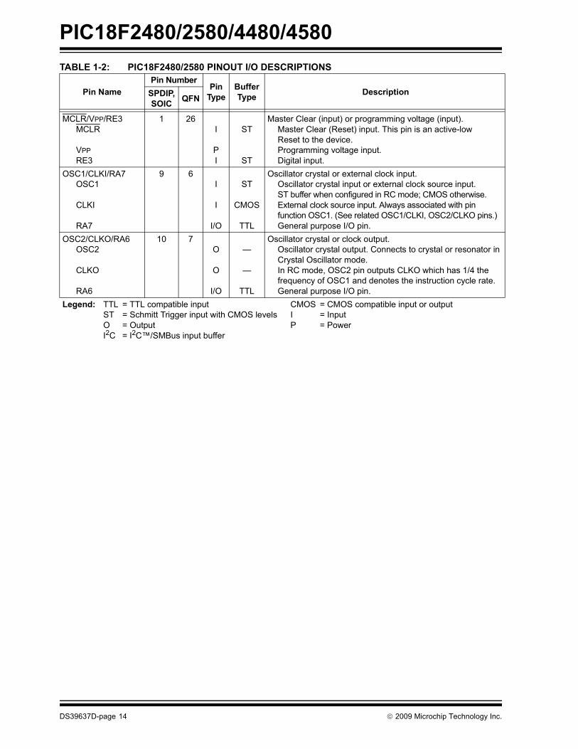
TABLE 1-2: PIC18F2480/2580 PINOUT I/O DESCRIPTIONSPin NamePin Number
PinType
BufferType DescriptionSPDIP,
SOIC QFN
MCLR/VPP/RE3MCLR
VPPRE3
1 26I
PI
ST
ST
Master Clear (input) or programming voltage (input).Master Clear (Reset) input. This pin is an active-low Reset to the device.Programming voltage input.Digital input.
OSC1/CLKI/RA7OSC1
CLKI
RA7
9 6I
I
I/O
ST
CMOS
TTL
Oscillator crystal or external clock input.Oscillator crystal input or external clock source input. ST buffer when configured in RC mode; CMOS otherwise.External clock source input. Always associated with pin function OSC1. (See related OSC1/CLKI, OSC2/CLKO pins.)General purpose I/O pin.
OSC2/CLKO/RA6OSC2
CLKO
RA6
10 7O
O
I/O
—
—
TTL
Oscillator crystal or clock output.Oscillator crystal output. Connects to crystal or resonator in Crystal Oscillator mode.In RC mode, OSC2 pin outputs CLKO which has 1/4 the frequency of OSC1 and denotes the instruction cycle rate. General purpose I/O pin.
Legend: TTL = TTL compatible input CMOS = CMOS compatible input or output ST = Schmitt Trigger input with CMOS levels I = Input O = Output P = Power I2C = I2C™/SMBus input buffer
DS39637D-page 14 © 2009 Microchip Technology Inc.

PIC18F2480/2580/4480/4580
PORTA is a bidirectional I/O port.RA0/AN0
RA0AN0
2 27I/OI
TTLAnalog
Digital I/O.Analog Input 0.
RA1/AN1RA1AN1
3 28I/OI
TTLAnalog
Digital I/O.Analog Input 1.
RA2/AN2/VREF-RA2AN2VREF-
4 1I/OII
TTLAnalogAnalog
Digital I/O.Analog Input 2.A/D reference voltage (low) input.
RA3/AN3/VREF+RA3AN3VREF+
5 2I/OII
TTLAnalogAnalog
Digital I/O.Analog Input 3.A/D reference voltage (high) input.
RA4/T0CKIRA4T0CKI
6 3I/OI
TTLST
Digital I/O.Timer0 external clock input.
RA5/AN4/SS/HLVDIN
RA5AN4SSHLVDIN
7 4
I/OIII
TTLAnalog
TTLAnalog
Digital I/O.Analog Input 4. SPI slave select input.High/Low-Voltage Detect input.
RA6 See the OSC2/CLKO/RA6 pin.
RA7 See the OSC1/CLKI/RA7 pin.
TABLE 1-2: PIC18F2480/2580 PINOUT I/O DESCRIPTIONS (CONTINUED)
Pin NamePin Number
PinType
BufferType DescriptionSPDIP,
SOIC QFN
Legend: TTL = TTL compatible input CMOS = CMOS compatible input or output ST = Schmitt Trigger input with CMOS levels I = Input O = Output P = Power I2C = I2C™/SMBus input buffer
© 2009 Microchip Technology Inc. DS39637D-page 15

PIC18F2480/2580/4480/4580
PORTB is a bidirectional I/O port. PORTB can be software programmed for internal weak pull-ups on all inputs.
RB0/INT0/ AN10RB0INT0AN10
21 18I/OII
TTLST
Analog
Digital I/O.External Interrupt 0.Analog Input 10.
RB1/INT1/AN8RB1INT1AN8
22 19I/OII
TTLST
Analog
Digital I/O.External Interrupt 1.Analog Input 8.
RB2/INT2/CANTXRB2INT2CANTX
23 20I/OIO
TTLSTTTL
Digital I/O.External Interrupt 2.CAN bus TX.
RB3/CANRXRB3CANRX
24 21I/OI
TTLTTL
Digital I/O.CAN bus RX.
RB4/KBI0/AN9RB4KBI0AN9
25 22I/OII
TTLTTL
Analog
Digital I/O.Interrupt-on-change pin.Analog Input 9.
RB5/KBI1/PGMRB5KBI1PGM
26 23I/OI
I/O
TTLTTLST
Digital I/O.Interrupt-on-change pin.Low-Voltage ICSP™ Programming enable pin.
RB6/KBI2/PGCRB6KBI2PGC
27 24I/OI
I/O
TTLTTLST
Digital I/O.Interrupt-on-change pin. In-Circuit Debugger and ICSP programming clock pin.
RB7/KBI3/PGDRB7KBI3PGD
28 25I/OI
I/O
TTLTTLST
Digital I/O.Interrupt-on-change pin. In-Circuit Debugger and ICSP programming data pin.
TABLE 1-2: PIC18F2480/2580 PINOUT I/O DESCRIPTIONS (CONTINUED)
Pin NamePin Number
PinType
BufferType DescriptionSPDIP,
SOIC QFN
Legend: TTL = TTL compatible input CMOS = CMOS compatible input or output ST = Schmitt Trigger input with CMOS levels I = Input O = Output P = Power I2C = I2C™/SMBus input buffer
DS39637D-page 16 © 2009 Microchip Technology Inc.

PIC18F2480/2580/4480/4580
PORTC is a bidirectional I/O port.RC0/T1OSO/T13CKI
RC0T1OSOT13CKI
11 8I/OOI
ST—ST
Digital I/O.Timer1 oscillator output. Timer1/Timer3 external clock input.
RC1/T1OSIRC1T1OSI
12 9I/OI
STCMOS
Digital I/O.Timer1 oscillator input.
RC2/CCP1RC2CCP1
13 10I/OI/O
STST
Digital I/O.Capture 1 input/Compare 1 output/PWM1 output.
RC3/SCK/SCLRC3SCKSCL
14 11I/OI/OI/O
STSTI2C
Digital I/O.Synchronous serial clock input/output for SPI mode.Synchronous serial clock input/output for I2C™ mode.
RC4/SDI/SDARC4SDISDA
15 12I/OI
I/O
STSTI2C
Digital I/O.SPI data in.I2C data I/O.
RC5/SDORC5SDO
16 13I/OO
ST—
Digital I/O.SPI data out.
RC6/TX/CKRC6TXCK
17 14I/OO
I/O
ST—ST
Digital I/O.EUSART asynchronous transmit. EUSART synchronous clock (see related RX/DT).
RC7/RX/DTRC7RXDT
18 15I/OI
I/O
STSTST
Digital I/O.EUSART asynchronous receive.EUSART synchronous data (see related TX/CK).
RE3 — — — — See MCLR/VPP/RE3 pin.VSS 8, 19 5, 16 P — Ground reference for logic and I/O pins.VDD 20 17 P — Positive supply for logic and I/O pins.
TABLE 1-2: PIC18F2480/2580 PINOUT I/O DESCRIPTIONS (CONTINUED)
Pin NamePin Number
PinType
BufferType DescriptionSPDIP,
SOIC QFN
Legend: TTL = TTL compatible input CMOS = CMOS compatible input or output ST = Schmitt Trigger input with CMOS levels I = Input O = Output P = Power I2C = I2C™/SMBus input buffer
© 2009 Microchip Technology Inc. DS39637D-page 17

PIC18F2480/2580/4480/4580
TABLE 1-3: PIC18F4480/4580 PINOUT I/O DESCRIPTIONSPin NamePin Number Pin
TypeBufferType Description
PDIP QFN TQFP
MCLR/VPP/RE3MCLR
VPPRE3
1 18 18I
PI
ST
ST
Master Clear (input) or programming voltage (input).Master Clear (Reset) input. This pin is an active-low Reset to the device.Programming voltage input.Digital input.
OSC1/CLKI/RA7OSC1
CLKI
RA7
13 32 30I
I
I/O
ST
CMOS
TTL
Oscillator crystal or external clock input.Oscillator crystal input or external clock source input. ST buffer when configured in RC mode; CMOS otherwise.External clock source input. Always associated with pin function OSC1. (See related OSC1/CLKI, OSC2/CLKO pins.)General purpose I/O pin.
OSC2/CLKO/RA6OSC2
CLKO
RA6
14 33 31O
O
I/O
—
—
TTL
Oscillator crystal or clock output.Oscillator crystal output. Connects to crystal or resonator in Crystal Oscillator mode.In RC mode, OSC2 pin outputs CLKO which has 1/4 the frequency of OSC1 and denotes the instruction cycle rate. General purpose I/O pin.
Legend: TTL = TTL compatible input CMOS = CMOS compatible input or output ST = Schmitt Trigger input with CMOS levels I = Input O = Output P = Power I2C = I2C™/SMBus input buffer
DS39637D-page 18 © 2009 Microchip Technology Inc.

PIC18F2480/2580/4480/4580
PORTA is a bidirectional I/O port.RA0/AN0/CVREF
RA0AN0CVREF
2 19 19I/OIO
TTLAnalogAnalog
Digital I/O.Analog Input 0.Analog comparator reference output.
RA1/AN1RA1AN1
3 20 20I/OI
TTLAnalog
Digital I/O.Analog Input 1.
RA2/AN2/VREF-RA2AN2VREF-
4 21 21I/OII
TTLAnalogAnalog
Digital I/O.Analog Input 2.A/D reference voltage (low) input.
RA3/AN3/VREF+RA3AN3VREF+
5 22 22I/OII
TTLAnalogAnalog
Digital I/O.Analog Input 3.A/D reference voltage (high) input.
RA4/T0CKIRA4T0CKI
6 23 23I/OI
TTLST
Digital I/O.Timer0 external clock input.
RA5/AN4/SS/HLVDIN
RA5AN4SSHLVDIN
7 24 24
I/OIII
TTLAnalog
TTLAnalog
Digital I/O.Analog Input 4.SPI slave select input.High/Low-Voltage Detect input.
RA6 See the OSC2/CLKO/RA6 pin.RA7 See the OSC1/CLKI/RA7 pin.
TABLE 1-3: PIC18F4480/4580 PINOUT I/O DESCRIPTIONS (CONTINUED)
Pin NamePin Number Pin
TypeBufferType Description
PDIP QFN TQFP
Legend: TTL = TTL compatible input CMOS = CMOS compatible input or output ST = Schmitt Trigger input with CMOS levels I = Input O = Output P = Power I2C = I2C™/SMBus input buffer
© 2009 Microchip Technology Inc. DS39637D-page 19

PIC18F2480/2580/4480/4580
PORTB is a bidirectional I/O port. PORTB can be software programmed for internal weak pull-ups on all inputs.
RB0/INT0/FLT0/AN10
RB0INT0FLT0AN10
33 9 8I/OIII
TTLSTST
Analog
Digital I/O.External Interrupt 0.Enhanced PWM Fault input (ECCP1 module).Analog input 10.
RB1/INT1/AN8RB1INT1AN8
34 10 9I/OII
TTLST
Analog
Digital I/O.External Interrupt 1.Analog input 8.
RB2/INT2/CANTXRB2INT2CANTX
35 11 10I/OIO
TTLSTTTL
Digital I/O.External Interrupt 2.CAN bus TX.
RB3/CANRXRB3CANRX
36 12 11I/OI
TTLTTL
Digital I/O.CAN bus RX.
RB4/KBI0/AN9RB4KBI0AN9
37 14 14I/OII
TTLTTL
Analog
Digital I/O.Interrupt-on-change pin.Analog Input 9.
RB5/KBI1/PGMRB5KBI1PGM
38 15 15I/OI
I/O
TTLTTLST
Digital I/O.Interrupt-on-change pin.Low-Voltage ICSP™ Programming enable pin.
RB6/KBI2/PGCRB6KBI2PGC
39 16 16I/OI
I/O
TTLTTLST
Digital I/O.Interrupt-on-change pin. In-Circuit Debugger and ICSP programmingclock pin.
RB7/KBI3/PGDRB7KBI3PGD
40 17 17I/OI
I/O
TTLTTLST
Digital I/O.Interrupt-on-change pin. In-Circuit Debugger and ICSP programmingdata pin.
TABLE 1-3: PIC18F4480/4580 PINOUT I/O DESCRIPTIONS (CONTINUED)
Pin NamePin Number Pin
TypeBufferType Description
PDIP QFN TQFP
Legend: TTL = TTL compatible input CMOS = CMOS compatible input or output ST = Schmitt Trigger input with CMOS levels I = Input O = Output P = Power I2C = I2C™/SMBus input buffer
DS39637D-page 20 © 2009 Microchip Technology Inc.

PIC18F2480/2580/4480/4580
PORTC is a bidirectional I/O port.RC0/T1OSO/T13CKI
RC0T1OSOT13CKI
15 34 32I/OOI
ST—ST
Digital I/O.Timer1 oscillator output. Timer1/Timer3 external clock input.
RC1/T1OSIRC1T1OSI
16 35 35I/OI
STCMOS
Digital I/O.Timer1 oscillator input.
RC2/CCP1RC2CCP1
17 36 36I/OI/O
STST
Digital I/O.Capture 1 input/Compare 1 output/PWM1 output.
RC3/SCK/SCLRC3SCK
SCL
18 37 37I/OI/O
I/O
STST
I2C
Digital I/O.Synchronous serial clock input/output for SPI mode.Synchronous serial clock input/output for I2C™ mode.
RC4/SDI/SDARC4SDISDA
23 42 42I/OI
I/O
STSTI2C
Digital I/O.SPI data in.I2C data I/O.
RC5/SDORC5SDO
24 43 43I/OO
ST—
Digital I/O.SPI data out.
RC6/TX/CKRC6TXCK
25 44 44I/OO
I/O
ST—ST
Digital I/O.EUSART asynchronous transmit.EUSART synchronous clock (see related RX/DT).
RC7/RX/DTRC7RXDT
26 1 1I/OI
I/O
STSTST
Digital I/O.EUSART asynchronous receive.EUSART synchronous data (see related TX/CK).
TABLE 1-3: PIC18F4480/4580 PINOUT I/O DESCRIPTIONS (CONTINUED)
Pin NamePin Number Pin
TypeBufferType Description
PDIP QFN TQFP
Legend: TTL = TTL compatible input CMOS = CMOS compatible input or output ST = Schmitt Trigger input with CMOS levels I = Input O = Output P = Power I2C = I2C™/SMBus input buffer
© 2009 Microchip Technology Inc. DS39637D-page 21

PIC18F2480/2580/4480/4580
PORTD is a bidirectional I/O port or a Parallel Slave Port (PSP) for interfacing to a microprocessor port. These pins have TTL input buffers when the PSP module is enabled.
RD0/PSP0/C1IN+RD0PSP0C1IN+
19 38 38I/OI/OI
STTTL
Analog
Digital I/O.Parallel Slave Port data.Comparator 1 input (+).
RD1/PSP1/C1IN-RD1PSP1C1IN-
20 39 39I/OI/OI
STTTL
Analog
Digital I/O.Parallel Slave Port data.Comparator 1 input (-)
RD2/PSP2/C2IN+RD2PSP2C2IN+
21 40 40I/OI/OI
STTTL
Analog
Digital I/O.Parallel Slave Port data.Comparator 2 input (+).
RD3/PSP3/C2IN-RD3PSP3C2IN-
22 41 41I/OI/OI
STTTL
Analog
Digital I/O.Parallel Slave Port data.Comparator 2 input (-).
RD4/PSP4/ECCP1/P1A
RD4PSP4ECCP1P1A
27 2 2
I/OI/OI/OO
STTTLSTTTL
Digital I/O.Parallel Slave Port data.Capture 2 input/Compare 2 output/PWM2 output.ECCP1 PWM Output A.
RD5/PSP5/P1BRD5PSP5P1B
28 3 3I/OI/OO
STTTLTTL
Digital I/O.Parallel Slave Port data.ECCP1 PWM Output B.
RD6/PSP6/P1CRD6PSP6P1C
29 4 4I/OI/OO
STTTLTTL
Digital I/O.Parallel Slave Port data.ECCP1 PWM Output C.
RD7/PSP7/P1DRD7PSP7P1D
30 5 5I/OI/OO
STTTLTTL
Digital I/O.Parallel Slave Port data.ECCP1 PWM Output D.
TABLE 1-3: PIC18F4480/4580 PINOUT I/O DESCRIPTIONS (CONTINUED)
Pin NamePin Number Pin
TypeBufferType Description
PDIP QFN TQFP
Legend: TTL = TTL compatible input CMOS = CMOS compatible input or output ST = Schmitt Trigger input with CMOS levels I = Input O = Output P = Power I2C = I2C™/SMBus input buffer
DS39637D-page 22 © 2009 Microchip Technology Inc.
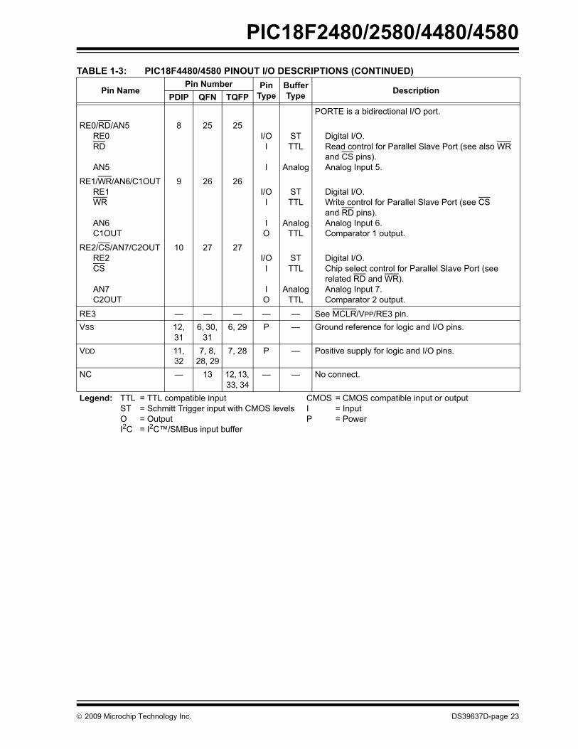
PIC18F2480/2580/4480/4580
PORTE is a bidirectional I/O port.
RE0/RD/AN5RE0RD
AN5
8 25 25I/OI
I
STTTL
Analog
Digital I/O.Read control for Parallel Slave Port (see also WR and CS pins).Analog Input 5.
RE1/WR/AN6/C1OUTRE1WR
AN6C1OUT
9 26 26I/OI
IO
STTTL
AnalogTTL
Digital I/O.Write control for Parallel Slave Port (see CS and RD pins).Analog Input 6.Comparator 1 output.
RE2/CS/AN7/C2OUTRE2CS
AN7C2OUT
10 27 27I/OI
IO
STTTL
AnalogTTL
Digital I/O.Chip select control for Parallel Slave Port (see related RD and WR).Analog Input 7.Comparator 2 output.
RE3 — — — — — See MCLR/VPP/RE3 pin.VSS 12,
316, 30,
316, 29 P — Ground reference for logic and I/O pins.
VDD 11, 32
7, 8, 28, 29
7, 28 P — Positive supply for logic and I/O pins.
NC — 13 12, 13, 33, 34
— — No connect.
TABLE 1-3: PIC18F4480/4580 PINOUT I/O DESCRIPTIONS (CONTINUED)
Pin NamePin Number Pin
TypeBufferType Description
PDIP QFN TQFP
Legend: TTL = TTL compatible input CMOS = CMOS compatible input or output ST = Schmitt Trigger input with CMOS levels I = Input O = Output P = Power I2C = I2C™/SMBus input buffer
© 2009 Microchip Technology Inc. DS39637D-page 23

PIC18F2480/2580/4480/4580
NOTES:DS39637D-page 24 © 2009 Microchip Technology Inc.

PIC18F2480/2580/4480/4580
2.0 GUIDELINES FOR GETTING STARTED WITH PIC18F MICROCONTROLLERS
2.1 Basic Connection RequirementsGetting started with the PIC18F2480/2580/4480/4580family of 8-bit microcontrollers requires attention to aminimal set of device pin connections beforeproceeding with development.
The following pins must always be connected:
• All VDD and VSS pins (see Section 2.2 “Power Supply Pins”)
• All AVDD and AVSS pins, regardless of whether or not the analog device features are used (see Section 2.2 “Power Supply Pins”)
• MCLR pin (see Section 2.3 “Master Clear (MCLR) Pin”)
These pins must also be connected if they are beingused in the end application:
• PGC/PGD pins used for In-Circuit Serial Programming™ (ICSP™) and debugging purposes (see Section 2.4 “ICSP Pins”)
• OSCI and OSCO pins when an external oscillator source is used (see Section 2.5 “External Oscillator Pins”)
Additionally, the following pins may be required:
• VREF+/VREF- pins are used when external voltage reference for analog modules is implemented
The minimum mandatory connections are shown inFigure 2-1.
FIGURE 2-1: RECOMMENDED MINIMUM CONNECTIONS
Note: The AVDD and AVSS pins must always beconnected, regardless of whether any ofthe analog modules are being used.
PIC18FXXXX
VD
D
VS
S
VDD
VSS
VSS
VDD
AVD
D
AVS
S
VD
D
VS
S
C1
R1
VDD
MCLRR2
C2(1)
C3(1)
C4(1)C5(1)
C6(1)
Key (all values are recommendations):C1 through C6: 0.1 µF, 20V ceramicR1: 10 kΩR2: 100Ω to 470ΩNote 1: The example shown is for a PIC18F device
with five VDD/VSS and AVDD/AVSS pairs. Other devices may have more or less pairs; adjust the number of decoupling capacitors appropriately.
© 2009 Microchip Technology Inc. DS39637D-page 25

PIC18F2480/2580/4480/4580
2.2 Power Supply Pins2.2.1 DECOUPLING CAPACITORSThe use of decoupling capacitors on every pair ofpower supply pins, such as VDD, VSS, AVDD andAVSS, is required.
Consider the following criteria when using decouplingcapacitors:
• Value and type of capacitor: A 0.1 μF (100 nF), 10-20V capacitor is recommended. The capacitor should be a low-ESR device, with a resonance frequency in the range of 200 MHz and higher. Ceramic capacitors are recommended.
• Placement on the printed circuit board: The decoupling capacitors should be placed as close to the pins as possible. It is recommended to place the capacitors on the same side of the board as the device. If space is constricted, the capacitor can be placed on another layer on the PCB using a via; however, ensure that the trace length from the pin to the capacitor is no greater than 0.25 inch (6 mm).
• Handling high-frequency noise: If the board is experiencing high-frequency noise (upward of tens of MHz), add a second ceramic type capaci-tor in parallel to the above described decoupling capacitor. The value of the second capacitor can be in the range of 0.01 μF to 0.001 μF. Place this second capacitor next to each primary decoupling capacitor. In high-speed circuit designs, consider implementing a decade pair of capacitances as close to the power and ground pins as possible (e.g., 0.1 μF in parallel with 0.001 μF).
• Maximizing performance: On the board layout from the power supply circuit, run the power and return traces to the decoupling capacitors first, and then to the device pins. This ensures that the decoupling capacitors are first in the power chain. Equally important is to keep the trace length between the capacitor and the power pins to a minimum, thereby reducing PCB trace inductance.
2.2.2 TANK CAPACITORSOn boards with power traces running longer thansix inches in length, it is suggested to use a tank capac-itor for integrated circuits, including microcontrollers, tosupply a local power source. The value of the tankcapacitor should be determined based on the traceresistance that connects the power supply source tothe device, and the maximum current drawn by thedevice in the application. In other words, select the tankcapacitor so that it meets the acceptable voltage sag atthe device. Typical values range from 4.7 μF to 47 μF.
2.2.3 CONSIDERATIONS WHEN USING BOR
When the Brown-out Reset (BOR) feature is enabled,a sudden change in VDD may result in a spontaneousBOR event. This can happen when the microcontrolleris operating under normal operating conditions, regard-less of what the BOR set point has been programmedto, and even if VDD does not approach the set point.The precipitating factor in these BOR events is a rise orfall in VDD with a slew rate faster than 0.15V/μs.
An application that incorporates adequate decouplingbetween the power supplies will not experience suchrapid voltage changes. Additionally, the use of anelectrolytic tank capacitor across VDD and VSS, asdescribed above, will be helpful in preventing high slewrate transitions.
If the application has components that turn on or off,and share the same VDD circuit as the microcontroller,the BOR can be disabled in software by using theSBOREN bit before switching the component. After-wards, allow a small delay before re-enabling the BOR.By doing this, it is ensured that the BOR is disabledduring the interval that might cause high slew ratechanges of VDD.
Note: Not all devices incorporate software BORcontrol. See Section 5.0 “Reset” fordevice-specific information.
DS39637D-page 26 © 2009 Microchip Technology Inc.

PIC18F2480/2580/4480/4580
2.3 Master Clear (MCLR) PinThe MCLR pin provides two specific devicefunctions: Device Reset, and Device Programmingand Debugging. If programming and debugging arenot required in the end application, a directconnection to VDD may be all that is required. Theaddition of other components, to help increase theapplication’s resistance to spurious Resets fromvoltage sags, may be beneficial. A typicalconfiguration is shown in Figure 2-1. Other circuitdesigns may be implemented, depending on theapplication’s requirements.During programming and debugging, the resistanceand capacitance that can be added to the pin must beconsidered. Device programmers and debuggers drivethe MCLR pin. Consequently, specific voltage levels(VIH and VIL) and fast signal transitions must not beadversely affected. Therefore, specific values of R1and C1 will need to be adjusted based on theapplication and PCB requirements. For example, it isrecommended that the capacitor, C1, be isolated fromthe MCLR pin during programming and debuggingoperations by using a jumper (Figure 2-2). The jumperis replaced for normal run-time operations.
Any components associated with the MCLR pinshould be placed within 0.25 inch (6 mm) of the pin.
FIGURE 2-2: EXAMPLE OF MCLR PIN CONNECTIONS
2.4 ICSP PinsThe PGC and PGD pins are used for In-Circuit SerialProgramming™ (ICSP™) and debugging purposes. Itis recommended to keep the trace length between theICSP connector and the ICSP pins on the device asshort as possible. If the ICSP connector is expected toexperience an ESD event, a series resistor is recom-mended, with the value in the range of a few tens ofohms, not to exceed 100Ω.
Pull-up resistors, series diodes, and capacitors on thePGC and PGD pins are not recommended as they willinterfere with the programmer/debugger communica-tions to the device. If such discrete components are anapplication requirement, they should be removed fromthe circuit during programming and debugging. Alter-natively, refer to the AC/DC characteristics and timingrequirements information in the respective deviceFlash programming specification for information oncapacitive loading limits and pin input voltage high (VIH)and input low (VIL) requirements.
For device emulation, ensure that the “CommunicationChannel Select” (i.e., PGCx/PGDx pins) programmedinto the device matches the physical connections forthe ICSP to the Microchip debugger/emulator tool.
For more information on available Microchipdevelopment tools connection requirements, refer toSection 27.0 “Development Support”.
Note 1: R1 ≤ 10 kΩ is recommended. A suggestedstarting value is 10 kΩ. Ensure that theMCLR pin VIH and VIL specifications are met.
2: R2 ≤ 470Ω will limit any current flowing intoMCLR from the external capacitor, C, in theevent of MCLR pin breakdown, due toElectrostatic Discharge (ESD) or ElectricalOverstress (EOS). Ensure that the MCLR pinVIH and VIL specifications are met.
C1
R2R1
VDD
MCLR
PIC18FXXXXJP
© 2009 Microchip Technology Inc. DS39637D-page 27

PIC18F2480/2580/4480/4580
2.5 External Oscillator PinsMany microcontrollers have options for at least twooscillators: a high-frequency primary oscillator and alow-frequency secondary oscillator (refer toSection 3.0 “Oscillator Configurations” for details).The oscillator circuit should be placed on the sameside of the board as the device. Place the oscillatorcircuit close to the respective oscillator pins with nomore than 0.5 inch (12 mm) between the circuitcomponents and the pins. The load capacitors shouldbe placed next to the oscillator itself, on the same sideof the board.
Use a grounded copper pour around the oscillator cir-cuit to isolate it from surrounding circuits. Thegrounded copper pour should be routed directly to theMCU ground. Do not run any signal traces or powertraces inside the ground pour. Also, if using a two-sidedboard, avoid any traces on the other side of the boardwhere the crystal is placed.
Layout suggestions are shown in Figure 2-4. In-linepackages may be handled with a single-sided layoutthat completely encompasses the oscillator pins. Withfine-pitch packages, it is not always possible to com-pletely surround the pins and components. A suitablesolution is to tie the broken guard sections to a mirroredground layer. In all cases, the guard trace(s) must bereturned to ground.
In planning the application’s routing and I/O assign-ments, ensure that adjacent port pins and other signalsin close proximity to the oscillator are benign (i.e., freeof high frequencies, short rise and fall times, and othersimilar noise).
For additional information and design guidance onoscillator circuits, please refer to these MicrochipApplication Notes, available at the corporate web site(www.microchip.com):
• AN826, “Crystal Oscillator Basics and Crystal Selection for rfPIC™ and PICmicro® Devices”
• AN849, “Basic PICmicro® Oscillator Design”• AN943, “Practical PICmicro® Oscillator Analysis
and Design”• AN949, “Making Your Oscillator Work”
2.6 Unused I/OsUnused I/O pins should be configured as outputs anddriven to a logic low state. Alternatively, connect a 1 kΩto 10 kΩ resistor to VSS on unused pins and drive theoutput to logic low.
FIGURE 2-3: SUGGESTED PLACEMENT OF THE OSCILLATOR CIRCUIT
GND
`
`
`
OSC1
OSC2
T1OSO
T1OS I
Copper Pour Primary OscillatorCrystal
Timer1 OscillatorCrystal
DEVICE PINS
PrimaryOscillator
C1
C2
T1 Oscillator: C1 T1 Oscillator: C2
(tied to ground)
Single-Sided and In-Line Layouts:
Fine-Pitch (Dual-Sided) Layouts:
GND
OSCO
OSCI
Bottom LayerCopper Pour
OscillatorCrystal
Top Layer Copper Pour
C2
C1
DEVICE PINS
(tied to ground)
(tied to ground)
DS39637D-page 28 © 2009 Microchip Technology Inc.

PIC18F2480/2580/4480/4580
3.0 OSCILLATOR CONFIGURATIONS
3.1 Oscillator TypesPIC18F2480/2580/4480/4580 devices can be operatedin ten different oscillator modes. The user can programthe Configuration bits, FOSC<3:0>, in ConfigurationRegister 1H to select one of these ten modes:
1. LP Low-Power Crystal2. XT Crystal/Resonator3. HS High-Speed Crystal/Resonator4. HSPLL High-Speed Crystal/Resonator
with PLL Enabled5. RC External Resistor/Capacitor with
FOSC/4 Output on RA66. RCIO External Resistor/Capacitor with I/O
on RA67. INTIO1 Internal Oscillator with FOSC/4 Output
on RA6 and I/O on RA78. INTIO2 Internal Oscillator with I/O on RA6
and RA79. EC External Clock with FOSC/4 Output10. ECIO External Clock with I/O on RA6
3.2 Crystal Oscillator/Ceramic Resonators
In XT, LP, HS or HSPLL Oscillator modes, a crystal orceramic resonator is connected to the OSC1 andOSC2 pins to establish oscillation. Figure 3-1 showsthe pin connections.
The oscillator design requires the use of a parallelresonant crystal.
FIGURE 3-1: CRYSTAL/CERAMIC RESONATOR OPERATION (XT, LP, HS OR HSPLL CONFIGURATION)
TABLE 3-1: CAPACITOR SELECTION FOR CERAMIC RESONATORS
Note: Use of a series resonant crystal may givea frequency out of the crystalmanufacturer’s specifications.
Typical Capacitor Values Used:
Mode Freq OSC1 OSC2
XT 455 kHz2.0 MHz4.0 MHz
56 pF47 pF33 pF
56 pF47 pF33 pF
HS 8.0 MHz16.0 MHz
27 pF22 pF
27 pF22 pF
Capacitor values are for design guidance only. These capacitors were tested with the resonatorslisted below for basic start-up and operation. Thesevalues are not optimized.
Different capacitor values may be required to produceacceptable oscillator operation. The user should testthe performance of the oscillator over the expectedVDD and temperature range for the application.
See the notes on page 30 for additional information.
Resonators Used:
455 kHz 4.0 MHz2.0 MHz 8.0 MHz
16.0 MHz
Note: When using resonators with frequenciesabove 3.5 MHz, the use of HS mode,rather than XT mode, is recommended.HS mode may be used at any VDD forwhich the controller is rated. If HS isselected, it is possible that the gain of theoscillator will overdrive the resonator.Therefore, a series resistor should beplaced between the OSC2 pin and theresonator. As a good starting point, therecommended value of RS is 330Ω.
Note 1: See Table 3-1 and Table 3-2 for initial values of C1 and C2.
2: A series resistor (RS) may be required for AT strip cut crystals.
3: RF varies with the oscillator mode chosen.
C1(1)
C2(1)
XTAL
OSC2
OSC1
RF(3)
Sleep
To
Logic
PIC18FXXXXRS(2)
Internal
© 2009 Microchip Technology Inc. DS39637D-page 29

PIC18F2480/2580/4480/4580
TABLE 3-2: CAPACITOR SELECTION FORCRYSTAL OSCILLATOR
An external clock source may also be connected to theOSC1 pin in the HS mode, as shown in Figure 3-2.
FIGURE 3-2: EXTERNAL CLOCK INPUT OPERATION (HS OSCILLATOR CONFIGURATION)
3.3 External Clock InputThe EC and ECIO Oscillator modes require an externalclock source to be connected to the OSC1 pin. There isno oscillator start-up time required after a Power-onReset or after an exit from Sleep mode.
In the EC Oscillator mode, the oscillator frequencydivided by 4 is available on the OSC2 pin. This signalmay be used for test purposes or to synchronize otherlogic. Figure 3-3 shows the pin connections for the ECOscillator mode.
FIGURE 3-3: EXTERNAL CLOCK INPUT OPERATION (EC CONFIGURATION)
The ECIO Oscillator mode functions like the EC mode,except that the OSC2 pin becomes an additionalgeneral purpose I/O pin. The I/O pin becomes bit 6 ofPORTA (RA6). Figure 3-4 shows the pin connectionsfor the ECIO Oscillator mode.
FIGURE 3-4: EXTERNAL CLOCK INPUT OPERATION (ECIO CONFIGURATION)
Osc Type Crystal Freq
Typical Capacitor Values Tested:
C1 C2
LP 32 kHz 33 pF 33 pF200 kHz 15 pF 15 pF
XT 1 MHz 33 pF 33 pF4 MHz 27 pF 27 pF
HS 4 MHz 27 pF 27 pF8 MHz 22 pF 22 pF
20 MHz 15 pF 15 pFCapacitor values are for design guidance only. These capacitors were tested with the crystals listedbelow for basic start-up and operation. These valuesare not optimized.Different capacitor values may be required to produceacceptable oscillator operation. The user should testthe performance of the oscillator over the expectedVDD and temperature range for the application.
See the notes following this table for additionalinformation.
Crystals Used:32 kHz 4 MHz
200 kHz 8 MHz1 MHz 20 MHz
Note 1: Higher capacitance increases the stabilityof the oscillator but also increases thestart-up time.
2: When operating below 3V VDD, or whenusing certain ceramic resonators at anyvoltage, it may be necessary to use theHS mode or switch to a crystal oscillator.
3: Since each resonator/crystal has its owncharacteristics, the user should consultthe resonator/crystal manufacturer forappropriate values of externalcomponents.
4: Rs may be required to avoid overdrivingcrystals with low drive level specification.
5: Always verify oscillator performance overthe VDD and temperature range that isexpected for the application.
OSC1
OSC2Open
Clock fromExt. System PIC18FXXXX
(HS Mode)
OSC1/CLKI
OSC2/CLKOFOSC/4
Clock fromExt. System PIC18FXXXX
OSC1/CLKI
I/O (OSC2)RA6
Clock fromExt. System PIC18FXXXX
DS39637D-page 30 © 2009 Microchip Technology Inc.

PIC18F2480/2580/4480/4580
3.4 RC OscillatorFor timing insensitive applications, the “RC” and“RCIO” device options offer additional cost savings.The actual oscillator frequency is a function of severalfactors:• supply voltage• values of the external resistor (REXT) and
capacitor (CEXT)• operating temperature
Given the same device, operating voltage and tempera-ture and component values, there will also be unit-to-unitfrequency variations. These are due to factors such as:
• normal manufacturing variation• difference in lead frame capacitance between
package types (especially for low CEXT values) • variations within the tolerance of limits of REXT
and CEXT
In the RC Oscillator mode, the oscillator frequencydivided by 4 is available on the OSC2 pin. This signalmay be used for test purposes or to synchronize otherlogic. Figure 3-5 shows how the R/C combination isconnected.
FIGURE 3-5: RC OSCILLATOR MODE
The RCIO Oscillator mode (Figure 3-6) functions likethe RC mode, except that the OSC2 pin becomes anadditional general purpose I/O pin. The I/O pinbecomes bit 6 of PORTA (RA6).
FIGURE 3-6: RCIO OSCILLATOR MODE
3.5 PLL Frequency MultiplierA Phase Locked Loop (PLL) circuit is provided as anoption for users who wish to use a lower frequencyoscillator circuit or to clock the device up to its highestrated frequency from a crystal oscillator. This may beuseful for customers who are concerned with EMI dueto high-frequency crystals or users who require higherclock speeds from an internal oscillator.
3.5.1 HSPLL OSCILLATOR MODEThe HSPLL mode makes use of the HS mode oscillatorfor frequencies up to 10 MHz. A PLL then multiplies theoscillator output frequency by 4 to produce an internalclock frequency up to 40 MHz.
The PLL is only available to the crystal oscillator whenthe FOSC<3:0> Configuration bits are programmed forHSPLL mode (= 0110).
FIGURE 3-7: PLL BLOCK DIAGRAM (HS MODE)
3.5.2 PLL AND INTOSCThe PLL is also available to the internal oscillator blockin selected oscillator modes. In this configuration, thePLL is enabled in software and generates a clockoutput of up to 32 MHz. The operation of INTOSC withthe PLL is described in Section 3.6.4 “PLL in INTOSCModes”.
OSC2/CLKO
CEXT
REXT
PIC18FXXXX
OSC1
FOSC/4
InternalClock
VDD
VSS
Recommended values: 3 kΩ ≤ REXT ≤ 100 kΩCEXT > 20 pF
CEXT
REXT
PIC18FXXXX
OSC1 InternalClock
VDD
VSS
Recommended values: 3 kΩ ≤ REXT ≤ 100 kΩCEXT > 20 pF
I/O (OSC2)RA6
MU
X
VCO
LoopFilter
CrystalOsc
OSC2
OSC1
PLL Enable
FIN
FOUT
SYSCLK
PhaseComparator
HS Osc Enable
÷4
(from Configuration Register 1H)
HS Mode
© 2009 Microchip Technology Inc. DS39637D-page 31

PIC18F2480/2580/4480/4580
3.6 Internal Oscillator BlockThe PIC18F2480/2580/4480/4580 devices include aninternal oscillator block which generates two differentclock signals; either can be used as the micro-controller’s clock source. This may eliminate the needfor external oscillator circuits on the OSC1 and/orOSC2 pins.The main output (INTOSC) is an 8 MHz clock source,which can be used to directly drive the device clock. Italso drives a postscaler, which can provide a range ofclock frequencies from 31 kHz to 4 MHz. The INTOSCoutput is enabled when a clock frequency from 125 kHzto 8 MHz is selected.
The other clock source is the internal RC oscillator(INTRC), which provides a nominal 31 kHz output.INTRC is enabled if it is selected as the device clocksource; it is also enabled automatically when any of thefollowing are enabled:
• Power-up Timer• Fail-Safe Clock Monitor• Watchdog Timer• Two-Speed Start-up
These features are discussed in greater detail inSection 25.0 “Special Features of the CPU”.
The clock source frequency (INTOSC direct, INTRCdirect or INTOSC postscaler) is selected by configuringthe IRCF bits of the OSCCON register (Register 3-2).
3.6.1 INTIO MODESUsing the internal oscillator as the clock source elimi-nates the need for up to two external oscillator pins,which can then be used for digital I/O. Two distinctconfigurations are available:
• In INTIO1 mode, the OSC2 pin outputs FOSC/4, while OSC1 functions as RA7 for digital input and output.
• In INTIO2 mode, OSC1 functions as RA7 and OSC2 functions as RA6, both for digital input and output.
3.6.2 INTOSC OUTPUT FREQUENCYThe internal oscillator block is calibrated at the factoryto produce an INTOSC output frequency of 8.0 MHz.
The INTRC oscillator operates independently of theINTOSC source. Any changes in INTOSC across volt-age and temperature are not necessarily reflected bychanges in INTRC and vice versa.
3.6.3 OSCTUNE REGISTERThe internal oscillator’s output has been calibrated atthe factory but can be adjusted in the user’s applica-tion. This is done by writing to the OSCTUNE register(Register 3-1).
When the OSCTUNE register is modified, the INTOSCand INTRC frequencies will begin shifting to the newfrequency. The INTRC clock will reach the newfrequency within 8 clock cycles (approximately8 * 32 μs = 256 μs). Code execution continues duringthis shift. There is no indication that the shift hasoccurred.
The OSCTUNE register also implements the INTSRCand PLLEN bits, which control certain features of theinternal oscillator block. The INTSRC bit allows usersto select which internal oscillator provides the clocksource when the 31 kHz frequency option is selected.This is covered in greater detail in Section 3.7.1“Oscillator Control Register”.
The PLLEN bit controls the operation of the frequencymultiplier, PLL, in internal oscillator modes.
3.6.4 PLL IN INTOSC MODESThe 4x frequency multiplier can be used with the inter-nal oscillator block to produce faster device clockspeeds than are normally possible with an internaloscillator. When enabled, the PLL produces a clockspeed of up to 32 MHz.
Unlike HSPLL mode, the PLL is controlled throughsoftware. The control bit, PLLEN (OSCTUNE<6>), isused to enable or disable its operation. If PLL isenabled and a Two-Speed Start-up from wake isperformed, execution is delayed until the PLL starts.
The PLL is available when the device is configured touse the internal oscillator block as its primary clocksource (FOSC<3:0> = 1001 or 1000). Additionally, thePLL will only function when the selected output fre-quency is either 4 MHz or 8 MHz (OSCCON<6:4> = 111or 110). If both of these conditions are not met, the PLLis disabled.
The PLLEN control bit is only functional in those internaloscillator modes where the PLL is available. In all othermodes, it is forced to ‘0’ and is effectively unavailable.
3.6.5 INTOSC FREQUENCY DRIFTThe factory calibrates the internal oscillator blockoutput (INTOSC) for 8 MHz. However, this frequencymay drift as VDD or temperature changes, which canaffect the controller operation in a variety of ways. It ispossible to adjust the INTOSC frequency by modifyingthe value in the OSCTUNE register. This has no effecton the INTRC clock source frequency.
Tuning the INTOSC source requires knowing when tomake the adjustment, in which direction it should bemade, and in some cases, how large a change isneeded. Three compensation techniques arediscussed in Section 3.6.5.1 “Compensating withthe EUSART”, Section 3.6.5.2 “Compensating withthe Timers” and Section 3.6.5.3 “Compensatingwith the CCP Module in Capture Mode”, but othertechniques may be used.
DS39637D-page 32 © 2009 Microchip Technology Inc.

PIC18F2480/2580/4480/4580
3.6.5.1 Compensating with the EUSART An adjustment may be required when the EUSARTbegins to generate framing errors or receives data witherrors while in Asynchronous mode. Framing errorsindicate that the device clock frequency is too high. Toadjust for this, decrement the value in OSCTUNE toreduce the clock frequency. On the other hand, errorsin data may suggest that the clock speed is too low. Tocompensate, increment OSCTUNE to increase theclock frequency.
3.6.5.2 Compensating with the TimersThis technique compares device clock speed to somereference clock. Two timers may be used; one timer isclocked by the peripheral clock, while the other isclocked by a fixed reference source, such as theTimer1 oscillator.
Both timers are cleared, but the timer clocked by thereference generates interrupts. When an interruptoccurs, the internally clocked timer is read and bothtimers are cleared. If the internally clocked timer value
is greater than expected, then the internal oscillatorblock is running too fast. To adjust for this, decrementthe OSCTUNE register.
3.6.5.3 Compensating with the CCP Module in Capture Mode
A CCP module can use free-running Timer1 (orTimer3), clocked by the internal oscillator block and anexternal event with a known period (i.e., AC powerfrequency). The time of the first event is captured in theCCPRxH:CCPRxL registers and is recorded for uselater. When the second event causes a capture, thetime of the first event is subtracted from the time of thesecond event. Since the period of the external event isknown, the time difference between events can becalculated.
If the measured time is much greater than thecalculated time, the internal oscillator block is runningtoo fast. To compensate, decrement the OSCTUNEregister. If the measured time is much less than thecalculated time, the internal oscillator block is runningtoo slow. To compensate, increment the OSCTUNEregister.
REGISTER 3-1: OSCTUNE: OSCILLATOR TUNING REGISTER
R/W-0 R/W-0(1) U-0 R/W-0 R/W-0 R/W-0 R/W-0 R/W-0 INTSRC PLLEN(1) — TUN4 TUN3 TUN2 TUN1 TUN0
bit 7 bit 0
Legend:R = Readable bit W = Writable bit U = Unimplemented bit, read as ‘0’-n = Value at POR ‘1’ = Bit is set ‘0’ = Bit is cleared x = Bit is unknown
bit 7 INTSRC: Internal Oscillator Low-Frequency Source Select bit1 = 31.25 kHz device clock derived from 8 MHz INTOSC source (divide-by-256 enabled)0 = 31 kHz device clock derived directly from INTRC internal oscillator
bit 6 PLLEN: Frequency Multiplier PLL for INTOSC Enable bit(1)
1 = PLL enabled for INTOSC (4 MHz and 8 MHz only)0 = PLL disabled
bit 5 Unimplemented: Read as ‘0’bit 4-0 TUN<4:0>: Frequency Tuning bits
01111 = Maximum frequency• •• •00001 00000 = Center frequency. Oscillator module is running at the calibrated frequency.11111 • •• •10000 = Minimum frequency
Note 1: Available only in certain oscillator configurations; otherwise, this bit is unavailable and reads as ‘0’. See text for details.
© 2009 Microchip Technology Inc. DS39637D-page 33

PIC18F2480/2580/4480/4580
3.7 Clock Sources and OscillatorSwitchingLike previous PIC18 devices, thePIC18F2480/2580/4480/4580 family includes a featurethat allows the device clock source to be switched fromthe main oscillator to an alternate low-frequency clocksource. PIC18F2480/2580/4480/4580 devices offertwo alternate clock sources. When an alternate clocksource is enabled, the various power-managedoperating modes are available.
Essentially, there are three clock sources for thesedevices:
• Primary oscillators• Secondary oscillators• Internal oscillator block
The primary oscillators include the external crystaland resonator modes, the external RC modes, theexternal clock modes and the internal oscillator block.The particular mode is defined by the FOSC<3:0>Configuration bits. The details of these modes arecovered earlier in this chapter.
The secondary oscillators are those external sourcesnot connected to the OSC1 or OSC2 pins. Thesesources may continue to operate even after thecontroller is placed in a power-managed mode.
PIC18F2480/2580/4480/4580 devices offer the Timer1oscillator as a secondary oscillator. This oscillator, in allpower-managed modes, is often the time base forfunctions such as a Real-Time Clock (RTC).
Most often, a 32.768 kHz watch crystal is connectedbetween the RC0/T1OSO/T13CKI and RC1/T1OSIpins. Like the LP Oscillator mode circuit, loadingcapacitors are also connected from each pin to ground.
The Timer1 oscillator is discussed in greater detail inSection 13.3 “Timer1 Oscillator”.
In addition to being a primary clock source, the internaloscillator block is available as a power-managedmode clock source. The INTRC source is also used asthe clock source for several special features, such asthe WDT and Fail-Safe Clock Monitor.
The clock sources for the PIC18F2480/2580/4480/4580devices are shown in Figure 3-8. See Section 25.0“Special Features of the CPU” for Configurationregister details.
FIGURE 3-8: PIC18F2480/2580/4480/4580 CLOCK DIAGRAM
4 x PLL
FOSC<3:0>
Secondary Oscillator
T1OSCENEnableOscillator
T1OSO
T1OSI
Clock Source Option for Other Modules
OSC1
OSC2
Sleep
Primary Oscillator
HSPLL, INTOSC/PLL
LP, XT, HS, RC, EC
T1OSC
CPU
Peripherals
IDLEN
Pos
tsca
ler
MU
X
MU
X
8 MHz
4 MHz
2 MHz
1 MHz
500 kHz
125 kHz
250 kHz
OSCCON<6:4>
111
110
101
100
011
010
001
00031 kHz
INTRCSource
InternalOscillator
Block
WDT, PWRT, FSCM
8 MHz
Internal Oscillator
(INTOSC)
OSCCON<6:4>
ClockControl
OSCCON<1:0>
Source8 MHz
31 kHz (INTRC)
OSCTUNE<6>
01
OSCTUNE<7>
and Two-Speed Start-up
DS39637D-page 34 © 2009 Microchip Technology Inc.
PIC18F2480/2580/4480/4580
3.7.1 OSCILLATOR CONTROL REGISTERThe OSCCON register (Register 3-2) controls severalaspects of the device clock’s operation, both infull-power operation and in power-managed modes.The System Clock Select bits, SCS<1:0>, select theclock source. The available clock sources are theprimary clock (defined by the FOSC<3:0> Configura-tion bits), the secondary clock (Timer1 oscillator) andthe internal oscillator block. The clock source changesimmediately after one or more of the bits is written to,following a brief clock transition interval. The SCS bitsare cleared on all forms of Reset.
The Internal Oscillator Frequency Select bits,IRCF<2:0>, select the frequency output of the internaloscillator block to drive the device clock. The choicesare the INTRC source, the INTOSC source (8 MHz) orone of the frequencies derived from the INTOSC post-scaler (31 kHz to 4 MHz). If the internal oscillator blockis supplying the device clock, changing the states ofthese bits will have an immediate change on the inter-nal oscillator’s output. On device Resets, the defaultoutput frequency of the internal oscillator block is set at1 MHz.
When an output frequency of 31 kHz is selected(IRCF<2:0> = 000), users may choose which internaloscillator acts as the source. This is done with theINTSRC bit in the OSCTUNE register (OSCTUNE<7>).Setting this bit selects INTOSC as a 31.25 kHz clocksource by enabling the divide-by-256 output of theINTOSC postscaler. Clearing INTSRC selects INTRC(nominally 31 kHz) as the clock source.
This option allows users to select the tunable and moreprecise INTOSC as a clock source, while maintainingpower savings with a very low clock speed. Regardlessof the setting of INTSRC, INTRC always remains theclock source for features such as the Watchdog Timerand the Fail-Safe Clock Monitor.
The OSTS, IOFS and T1RUN bits indicate which clocksource is currently providing the device clock. TheOSTS bit indicates that the Oscillator Start-up Timer(OST) has timed out and the primary clock is providingthe device clock in primary clock modes. The IOFS bitindicates when the internal oscillator block has stabi-lized and is providing the device clock in RC Clockmodes. The T1RUN bit (T1CON<6>) indicates whenthe Timer1 oscillator is providing the device clock insecondary clock modes. In power-managed modes,only one of these three bits will be set at any time. Ifnone of these bits are set, the INTRC is providing theclock or the internal oscillator block has just started andis not yet stable.
The IDLEN bit determines if the device goes into Sleepmode or one of the Idle modes when the SLEEPinstruction is executed.
The use of the flag and control bits in the OSCCONregister is discussed in more detail in Section 4.0“Power-Managed Modes”.
3.7.2 OSCILLATOR TRANSITIONSPIC18F2480/2580/4480/4580 devices contain circuitryto prevent clock “glitches” when switching betweenclock sources. A short pause in the device clock occursduring the clock switch. The length of this pause is thesum of two cycles of the old clock source and three tofour cycles of the new clock source. This formulaassumes that the new clock source is stable.
Clock transitions are discussed in greater detail inSection 4.1.2 “Entering Power-Managed Modes”.
Note 1: The Timer1 oscillator must be enabled toselect the secondary clock source. TheTimer1 oscillator is enabled by setting theT1OSCEN bit in the Timer1 Control regis-ter (T1CON<3>). If the Timer1 oscillator isnot enabled, then any attempt to select asecondary clock source when executing aSLEEP instruction will be ignored.
2: It is recommended that the Timer1oscillator be operating and stable beforeexecuting the SLEEP instruction, or a verylong delay may occur while the Timer1oscillator starts.
© 2009 Microchip Technology Inc. DS39637D-page 35

PIC18F2480/2580/4480/4580
REGISTER 3-2: OSCCON: OSCILLATOR CONTROL REGISTERR/W-0 R/W-1 R/W-0 R/W-0 R(1) R-0 R/W-0 R/W-0IDLEN IRCF2 IRCF1 IRCF0 OSTS IOFS SCS1 SCS0
bit 7 bit 0
Legend:R = Readable bit W = Writable bit U = Unimplemented bit, read as ‘0’-n = Value at POR ‘1’ = Bit is set ‘0’ = Bit is cleared x = Bit is unknown
bit 7 IDLEN: Idle Enable bit1 = Device enters Idle mode on SLEEP instruction0 = Device enters Sleep mode on SLEEP instruction
bit 6-4 IRCF<2:0>: Internal Oscillator Frequency Select bits111 = 8 MHz (INTOSC drives clock directly)110 = 4 MHz 101 = 2 MHz 100 = 1 MHz(3) 011 = 500 kHz 010 = 250 kHz001 = 125 kHz000 = 31 kHz (from either INTOSC/256 or INTRC directly)(2)
bit 3 OSTS: Oscillator Start-up Timer Time-out Status bit(1)
1 = Oscillator Start-up Timer time-out has expired; primary oscillator is running0 = Oscillator Start-up Timer time-out is running; primary oscillator is not ready
bit 2 IOFS: INTOSC Frequency Stable bit 1 = INTOSC frequency is stable and the frequency is provided by one of the RC modes0 = INTOSC frequency is not stable
bit 1-0 SCS<1:0>: System Clock Select bits1x = Internal oscillator block01 = Timer1 oscillator00 = Primary oscillator
Note 1: Depends on state of the IESO Configuration bit.2: Source selected by the INTSRC bit (OSCTUNE<7>), see text.3: Default output frequency of INTOSC on Reset.
DS39637D-page 36 © 2009 Microchip Technology Inc.

PIC18F2480/2580/4480/4580
3.8 Effects of Power-Managed Modeson the Various Clock SourcesWhen PRI_IDLE mode is selected, the designatedprimary oscillator continues to run without interruption.For all other power-managed modes, the oscillatorusing the OSC1 pin is disabled. The OSC1 pin (andOSC2 pin, if used by the oscillator) will stop oscillating.
In secondary clock modes (SEC_RUN andSEC_IDLE), the Timer1 oscillator is operating andproviding the device clock. The Timer1 oscillator mayalso run in all power-managed modes if required toclock Timer1 or Timer3.
In internal oscillator modes (RC_RUN and RC_IDLE),the internal oscillator block provides the device clocksource. The 31 kHz INTRC output can be used directlyto provide the clock and may be enabled to supportvarious special features, regardless of thepower-managed mode (see Section 25.2 “WatchdogTimer (WDT)”, Section 25.3 “Two-Speed Start-up”and Section 25.4 “Fail-Safe Clock Monitor” for moreinformation on WDT, Two-Speed Start-up and Fail-SafeClock Monitor. The INTOSC output at 8 MHz may beused directly to clock the device or may be divideddown by the postscaler. The INTOSC output is disabledif the clock is provided directly from the INTRC output.The INTOSC output is enabled for Two-Speed Start-upat 1 MHz after a Reset.
If the Sleep mode is selected, all clock sources arestopped. Since all the transistor switching currentshave been stopped, Sleep mode achieves the lowestcurrent consumption of the device (only leakagecurrents).
Enabling any on-chip feature that will operate duringSleep will increase the current consumed during Sleep.The INTRC is required to support WDT operation. The
Timer1 oscillator may be operating to support aReal-Time Clock (RTC). Other features may be operat-ing that do not require a device clock source (i.e.,MSSP slave, PSP, INTx pins and others). Peripheralsthat may add significant current consumption are listedin Section 28.2 “DC Characteristics: Power Downand Supply Current”.
3.9 Power-up DelaysPower-up delays are controlled by two timers, so that noexternal Reset circuitry is required for most applications.The delays ensure that the device is kept in Reset untilthe device power supply is stable under normal circum-stances and the primary clock is operating and stable.For additional information on power-up delays, seeSection 5.5 “Device Reset Timers”.
The first timer is the Power-up Timer (PWRT), whichprovides a fixed delay on power-up (parameter 33,Table 28-10). It is enabled by clearing (= 0) thePWRTEN Configuration bit.
The second timer is the Oscillator Start-up Timer(OST), intended to keep the chip in Reset until thecrystal oscillator is stable (LP, XT and HS modes). TheOST does this by counting 1024 oscillator cyclesbefore allowing the oscillator to clock the device.
When the HSPLL Oscillator mode is selected, thedevice is kept in Reset for an additional 2 ms, followingthe HS mode OST delay, so the PLL can lock to theincoming clock frequency.
There is a delay of interval, TCSD (parameter 38,Table 28-10), following POR, while the controllerbecomes ready to execute instructions. This delay runsconcurrently with any other delays. This may be theonly delay that occurs when any of the EC, RC or INTIOmodes are used as the primary clock source.
TABLE 3-3: OSC1 AND OSC2 PIN STATES IN SLEEP MODE OSC Mode OSC1 Pin OSC2 Pin
RC, INTIO1 Floating, external resistor should pull high At logic low (clock/4 output)RCIO, INTIO2 Floating, external resistor should pull high Configured as PORTA, bit 6ECIO Floating, pulled by external clock Configured as PORTA, bit 6EC Floating, pulled by external clock At logic low (clock/4 output)LP, XT and HS Feedback inverter disabled at quiescent
voltage levelFeedback inverter disabled at quiescent voltage level
Note: See Table 5-2 in Section 5.0 “Reset”, for time-outs due to Sleep and MCLR Reset.
© 2009 Microchip Technology Inc. DS39637D-page 37

PIC18F2480/2580/4480/4580
NOTES:DS39637D-page 38 © 2009 Microchip Technology Inc.

PIC18F2480/2580/4480/4580
4.0 POWER-MANAGED MODESPIC18F2480/2580/4480/4580 devices offer a total ofseven operating modes for more efficient powermanagement. These modes provide a variety ofoptions for selective power conservation in applicationswhere resources may be limited (i.e., battery-powereddevices).
There are three categories of power-managed modes:
• Run modes• Idle modes • Sleep mode
These categories define which portions of the deviceare clocked, and sometimes, what speed. The Run andIdle modes may use any of the three available clocksources (primary, secondary or internal oscillatorblock); the Sleep mode does not use a clock source.
The power-managed modes include severalpower-saving features offered on previous PIC®
devices. One is the clock switching feature, offered inother PIC18 devices, allowing the controller to use theTimer1 oscillator in place of the primary oscillator. Alsoincluded is the Sleep mode, offered by all PIC devices,where all device clocks are stopped.
4.1 Selecting Power-Managed ModesSelecting a power-managed mode requires twodecisions: if the CPU is to be clocked or not and theselection of a clock source. The IDLEN bit(OSCCON<7>) controls CPU clocking, while theSCS<1:0> bits (OSCCON<1:0>) select the clocksource. The individual modes, bit settings, clock sourcesand affected modules are summarized in Table 4-1.
4.1.1 CLOCK SOURCESThe SCS<1:0> bits allow the selection of one of threeclock sources for power-managed modes. They are:
• The primary clock, as defined by the FOSC<3:0> Configuration bits
• The secondary clock (the Timer1 oscillator)• The internal oscillator block (for RC modes)
4.1.2 ENTERING POWER-MANAGED MODES
Switching from one power-managed mode to anotherbegins by loading the OSCCON register. TheSCS<1:0> bits select the clock source and determinewhich Run or Idle mode is to be used. Changing thesebits causes an immediate switch to the new clocksource, assuming that it is running. The switch mayalso be subject to clock transition delays. These arediscussed in Section 4.1.3 “Clock Transitions andStatus Indicators” and subsequent sections.
Entry to the power-managed Idle or Sleep modes istriggered by the execution of a SLEEP instruction. Theactual mode that results depends on the status of theIDLEN bit.
Depending on the current mode and the mode beingswitched to, a change to a power-managed mode doesnot always require setting all of these bits. Manytransitions may be done by changing the oscillatorselect bits, or changing the IDLEN bit, prior to issuing aSLEEP instruction. If the IDLEN bit is alreadyconfigured correctly, it may only be necessary toperform a SLEEP instruction to switch to the desiredmode.
TABLE 4-1: POWER-MANAGED MODES
ModeOSCCON<7,1:0> Module Clocking
Available Clock and Oscillator SourceIDLEN(1) SCS<1:0> CPU Peripherals
Sleep 0 N/A Off Off None – All clocks are disabledPRI_RUN N/A 00 Clocked Clocked Primary – LP, XT, HS, HSPLL, RC, EC, INTRC(2):
This is the normal full-power execution mode.SEC_RUN N/A 01 Clocked Clocked Secondary – Timer1 OscillatorRC_RUN N/A 1x Clocked Clocked Internal Oscillator Block(2)
PRI_IDLE 1 00 Off Clocked Primary – LP, XT, HS, HSPLL, RC, ECSEC_IDLE 1 01 Off Clocked Secondary – Timer1 OscillatorRC_IDLE 1 1x Off Clocked Internal Oscillator Block(2)
Note 1: IDLEN reflects its value when the SLEEP instruction is executed.2: Includes INTOSC and INTOSC postscaler, as well as the INTRC source.
© 2009 Microchip Technology Inc. DS39637D-page 39

PIC18F2480/2580/4480/4580
4.1.3 CLOCK TRANSITIONS AND STATUSINDICATORSThe length of the transition between clock sources isthe sum of two cycles of the old clock source and threeto four cycles of the new clock source. This formulaassumes that the new clock source is stable.
Three bits indicate the current clock source and itsstatus. They are:
• OSTS (OSCCON<3>) • IOFS (OSCCON<2>) • T1RUN (T1CON<6>)
In general, only one of these bits will be set while in agiven power-managed mode. When the OSTS bit isset, the primary clock is providing the device clock.When the IOFS bit is set, the INTOSC output is provid-ing a stable 8 MHz clock source to a divider thatactually drives the device clock. When the T1RUN bit isset, the Timer1 oscillator is providing the clock. If noneof these bits are set, then either the INTRC clocksource is clocking the device, or the INTOSC source isnot yet stable.
If the internal oscillator block is configured as theprimary clock source by the FOSC<3:0> Configurationbits, then both the OSTS and IOFS bits may be setwhen in PRI_RUN or PRI_IDLE modes. This indicatesthat the primary clock (INTOSC output) is generating astable 8 MHz output. Entering another RCpower-managed mode at the same frequency wouldclear the OSTS bit.
4.1.4 MULTIPLE SLEEP COMMANDSThe power-managed mode that is invoked with theSLEEP instruction is determined by the setting of theIDLEN bit at the time the instruction is executed. Ifanother SLEEP instruction is executed, the device willenter the power-managed mode specified by IDLEN atthat time. If IDLEN has changed, the device will enter thenew power-managed mode specified by the new setting.
Upon resuming normal operation after waking formSleep or Idle, the internal state machines require atleast one TCY delay before another SLEEP instructioncan be executed. If two back-to-back SLEEP instruc-tions need to be executed, the process shown inExample 4-1 should be used.
EXAMPLE 4-1: EXECUTING BACK-TO-BACK SLEEP INSTRUCTIONS
4.2 Run ModesIn the Run modes, clocks to both the core andperipherals are active. The difference between thesemodes is the clock source.
4.2.1 PRI_RUN MODEThe PRI_RUN mode is the normal, full-power executionmode of the microcontroller. This is also the defaultmode upon a device Reset, unless Two-Speed Start-upis enabled (see Section 25.3 “Two-Speed Start-up” fordetails). In this mode, the OSTS bit is set. The IOFS bitmay be set if the internal oscillator block is the primaryclock source (see Section 3.7.1 “Oscillator ControlRegister”).
4.2.2 SEC_RUN MODEThe SEC_RUN mode is the compatible mode to the“clock switching” feature offered in other PIC18devices. In this mode, the CPU and peripherals areclocked from the Timer1 oscillator. This gives users theoption of lower power consumption while still using ahigh accuracy clock source.
SEC_RUN mode is entered by setting the SCS<1:0>bits to ‘01’. The device clock source is switched to theTimer1 oscillator (see Figure 4-1), the primary oscilla-tor is shut down, the T1RUN bit (T1CON<6>) is set andthe OSTS bit is cleared.
Note 1: Caution should be used when modifying asingle IRCF bit. If VDD is less than 3V, it ispossible to select a higher clock speedthan is supported by the low VDD.Improper device operation may result ifthe VDD/FOSC specifications are violated.
2: Executing a SLEEP instruction does notnecessarily place the device into Sleepmode. It acts as the trigger to place thecontroller into either the Sleep mode, orone of the Idle modes, depending on thesetting of the IDLEN bit.
Note: The Timer1 oscillator should already berunning prior to entering SEC_RUN mode.If the T1OSCEN bit is not set when theSCS<1:0> bits are set to ‘01’, entry toSEC_RUN mode will not occur. If theTimer1 oscillator is enabled but not yetrunning, device clocks will be delayed untilthe oscillator has started. In such situa-tions, initial oscillator operation is far fromstable and unpredictable operation mayresult.
SLEEPNOP ; Wait at least 1 Tcy before executing another SLEEP instruction
SLEEP
DS39637D-page 40 © 2009 Microchip Technology Inc.

PIC18F2480/2580/4480/4580
On transitions from SEC_RUN mode to PRI_RUNmode, the peripherals and CPU continue to be clockedfrom the Timer1 oscillator while the primary clock isstarted. When the primary clock becomes ready, aclock switch back to the primary clock occurs (seeFigure 4-2). When the clock switch is complete, theT1RUN bit is cleared, the OSTS bit is set and theprimary clock is providing the clock. The IDLEN andSCS bits are not affected by the wake-up; the Timer1oscillator continues to run.
FIGURE 4-1: TRANSITION TIMING FOR ENTRY TO SEC_RUN MODE
FIGURE 4-2: TRANSITION TIMING FROM SEC_RUN MODE TO PRI_RUN MODE (HSPLL)
4.2.3 RC_RUN MODEIn RC_RUN mode, the CPU and peripherals areclocked from the internal oscillator block using theINTOSC multiplexer; the primary clock is shut down.When using the INTRC source, this mode provides thebest power conservation of all the Run modes, whilestill executing code. It works well for user applicationswhich are not highly timing-sensitive or do not requirehigh-speed clocks at all times.
If the primary clock source is the internal oscillatorblock (either INTRC or INTOSC), there are no distin-guishable differences between PRI_RUN andRC_RUN modes during execution. However, a clockswitch delay will occur during entry to, and exit from,RC_RUN mode. Therefore, if the primary clock sourceis the internal oscillator block, the use of RC_RUNmode is not recommended.
This mode is entered by setting SCS1 to ‘1’. Althoughit is ignored, it is recommended that SCS0 also becleared; this is to maintain software compatibility withfuture devices. When the clock source is switched tothe INTOSC multiplexer (see Figure 4-3), the primaryoscillator is shut down and the OSTS bit is cleared. TheIRCF bits may be modified at any time to immediatelychange the clock speed.
Q4Q3Q2
OSC1
Peripheral
Program
Q1
T1OSI
Q1
Counter
Clock
CPUClock
PC + 2PC
1 2 3 n-1 n
Clock Transition
Q4Q3Q2 Q1 Q3Q2
PC + 4
Q1 Q3 Q4
OSC1
Peripheral
Program PC
T1OSI
PLL Clock
Q1
PC + 4
Q2
Output
Q3 Q4 Q1
CPU Clock
PC + 2
Clock
Counter
Q2 Q2 Q3
Note 1: TOST = 1024 TOSC; TPLL = 2 ms (approx). These intervals are not shown to scale.
SCS<1:0> Bits Changed
TOST(1)TPLL(1)
1 2 n-1 n
Clock
OSTS Bit Set
Transition
Note: Caution should be used when modifying asingle IRCF bit. If VDD is less than 3V, it ispossible to select a higher clock speedthan is supported by the low VDD.Improper device operation may result ifthe VDD/FOSC specifications are violated.
© 2009 Microchip Technology Inc. DS39637D-page 41

PIC18F2480/2580/4480/4580
If the IRCF bits and the INTSRC bit are all clear, theINTOSC output is not enabled and the IOFS bit willremain clear; there will be no indication of the currentclock source. The INTRC source is providing thedevice clocks.If the IRCF bits are changed from all clear (thus,enabling the INTOSC output) or if INTSRC is set, theIOFS bit becomes set after the INTOSC outputbecomes stable. Clocks to the device continue whilethe INTOSC source stabilizes after an interval ofTIOBST.
If the IRCF bits were previously at a non-zero value orif INTSRC was set before setting SCS1 and theINTOSC source was already stable, the IOFS bit willremain set.
On transitions from RC_RUN mode to PRI_RUN mode,the device continues to be clocked from the INTOSCmultiplexer while the primary clock is started. When theprimary clock becomes ready, a clock switch to theprimary clock occurs (see Figure 4-4). When the clockswitch is complete, the IOFS bit is cleared, the OSTSbit is set and the primary clock is providing the deviceclock. The IDLEN and SCS bits are not affected by theswitch. The INTRC source will continue to run if eitherthe WDT or the Fail-Safe Clock Monitor is enabled.
FIGURE 4-3: TRANSITION TIMING TO RC_RUN MODE
FIGURE 4-4: TRANSITION TIMING FROM RC_RUN MODE TO PRI_RUN MODE
Q4Q3Q2
OSC1
Peripheral
Program
Q1
INTRC
Q1
Counter
Clock
CPUClock
PC + 2PC
1 2 3 n-1 n
Clock Transition
Q4Q3Q2 Q1 Q3Q2
PC + 4
Q1 Q3 Q4
OSC1
Peripheral
Program PC
INTOSC
PLL Clock
Q1
PC + 4
Q2
Output
Q3 Q4 Q1
CPU Clock
PC + 2
Clock
Counter
Q2 Q2 Q3
Note 1: TOST = 1024 TOSC; TPLL = 2 ms (approx). These intervals are not shown to scale.
SCS<1:0> Bits Changed
TOST(1)TPLL(1)
1 2 n-1 n
Clock
OSTS Bit Set
Transition
Multiplexer
DS39637D-page 42 © 2009 Microchip Technology Inc.

PIC18F2480/2580/4480/4580
4.3 Sleep ModeThe power-managed Sleep mode in thePIC18F2480/2580/4480/4580 devices is identical tothe legacy Sleep mode offered in all other PIC devices.It is entered by clearing the IDLEN bit (the default stateon device Reset) and executing the SLEEP instruction.This shuts down the selected oscillator (Figure 4-5). Allclock source status bits are cleared.Entering the Sleep mode from any other mode does notrequire a clock switch. This is because no clocks areneeded once the controller has entered Sleep. If theWDT is selected, the INTRC source will continue tooperate. If the Timer1 oscillator is enabled, it will alsocontinue to run.
When a wake event occurs in Sleep mode (by interrupt,Reset or WDT time-out), the device will not be clockeduntil the clock source selected by the SCS1:SCS0 bitsbecomes ready (see Figure 4-6), or it will be clockedfrom the internal oscillator block if either the Two-SpeedStart-up or the Fail-Safe Clock Monitor are enabled(see Section 25.0 “Special Features of the CPU”). Ineither case, the OSTS bit is set when the primary clockis providing the device clocks. The IDLEN and SCS bitsare not affected by the wake-up.
4.4 Idle ModesThe Idle modes allow the controller’s CPU to beselectively shut down while the peripherals continue tooperate. Selecting a particular Idle mode allows usersto further manage power consumption.
If the IDLEN bit is set to ‘1’ when a SLEEP instruction isexecuted, the peripherals will be clocked from the clocksource selected using the SCS<1:0> bits; however, theCPU will not be clocked. The clock source status bits arenot affected. Setting IDLEN and executing a SLEEPinstruction provides a quick method of switching from agiven Run mode to its corresponding Idle mode.
If the WDT is selected, the INTRC source will continueto operate. If the Timer1 oscillator is enabled, it will alsocontinue to run.
Since the CPU is not executing instructions, the onlyexits from any of the Idle modes are by interrupt, WDTtime-out or a Reset. When a wake event occurs, CPUexecution is delayed by an interval of TCSD(parameter 38, Table 28-10) while it becomes ready toexecute code. When the CPU begins executing code,it resumes with the same clock source for the currentIdle mode. For example, when waking from RC_IDLEmode, the internal oscillator block will clock the CPUand peripherals (in other words, RC_RUN mode). TheIDLEN and SCS bits are not affected by the wake-up.
While in any Idle mode or Sleep mode, a WDT time-outwill result in a WDT wake-up to the Run mode currentlyspecified by the SCS<1:0> bits.
FIGURE 4-5: TRANSITION TIMING FOR ENTRY TO SLEEP MODE
FIGURE 4-6: TRANSITION TIMING FOR WAKE FROM SLEEP (HSPLL)
Q4Q3Q2
OSC1
Peripheral
Sleep
Program
Q1Q1
Counter
Clock
CPUClock
PC + 2PC
Q3 Q4 Q1 Q2
OSC1
Peripheral
Program PC
PLL Clock
Q3 Q4
Output
CPU Clock
Q1 Q2 Q3 Q4 Q1 Q2
Clock
Counter PC + 6PC + 4
Q1 Q2 Q3 Q4
Wake Event
Note1: TOST = 1024 TOSC; TPLL = 2 ms (approx). These intervals are not shown to scale.
TOST(1) TPLL(1)
OSTS Bit Set
PC + 2
© 2009 Microchip Technology Inc. DS39637D-page 43

PIC18F2480/2580/4480/4580
4.4.1 PRI_IDLE MODEThis mode is unique among the three low-power Idlemodes, in that it does not disable the primary deviceclock. For timing-sensitive applications, this allows forthe fastest resumption of device operation with its moreaccurate primary clock source, since the clock sourcedoes not have to “warm up” or transition from anotheroscillator.PRI_IDLE mode is entered from PRI_RUN mode bysetting the IDLEN bit and executing a SLEEP instruc-tion. If the device is in another Run mode, set IDLENfirst, then clear the SCS bits and execute SLEEP.Although the CPU is disabled, the peripherals continueto be clocked from the primary clock source specifiedby the FOSC<3:0> Configuration bits. The OSTS bitremains set (see Figure 4-7).
When a wake event occurs, the CPU is clocked from theprimary clock source. A delay of interval TCSD isrequired between the wake event and when codeexecution starts. This is required to allow the CPU tobecome ready to execute instructions. After thewake-up, the OSTS bit remains set. The IDLEN andSCS bits are not affected by the wake-up (seeFigure 4-8).
4.4.2 SEC_IDLE MODEIn SEC_IDLE mode, the CPU is disabled but theperipherals continue to be clocked from the Timer1oscillator. This mode is entered from SEC_RUN by set-ting the IDLEN bit and executing a SLEEP instruction. Ifthe device is in another Run mode, set the IDLEN bitfirst, then set the SCS<1:0> bits to ‘01’ and executeSLEEP. When the clock source is switched to theTimer1 oscillator, the primary oscillator is shut down,the OSTS bit is cleared and the T1RUN bit is set.
When a wake event occurs, the peripherals continue tobe clocked from the Timer1 oscillator. After an intervalof TCSD following the wake event, the CPU begins exe-cuting code being clocked by the Timer1 oscillator. TheIDLEN and SCS bits are not affected by the wake-up;the Timer1 oscillator continues to run (see Figure 4-8).
FIGURE 4-7: TRANSITION TIMING FOR ENTRY TO IDLE MODE
FIGURE 4-8: TRANSITION TIMING FOR WAKE FROM IDLE TO RUN MODE
Note: The Timer1 oscillator should already berunning prior to entering SEC_IDLE mode.If the T1OSCEN bit is not set when theSLEEP instruction is executed, the SLEEPinstruction will be ignored and entry toSEC_IDLE mode will not occur. If theTimer1 oscillator is enabled but not yetrunning, peripheral clocks will be delayeduntil the oscillator has started. In suchsituations, initial oscillator operation is farfrom stable and unpredictable operationmay result.
Q1
Peripheral
Program PC PC + 2
OSC1
Q3 Q4 Q1
CPU Clock
Clock
Counter
Q2
OSC1
Peripheral
Program PC
CPU Clock
Q1 Q3 Q4
Clock
Counter
Q2
Wake Event
TCSD
DS39637D-page 44 © 2009 Microchip Technology Inc.

PIC18F2480/2580/4480/4580
4.4.3 RC_IDLE MODEIn RC_IDLE mode, the CPU is disabled but the periph-erals continue to be clocked from the internal oscillatorblock using the INTOSC multiplexer. This mode allowsfor controllable power conservation during Idle periods.From RC_RUN, this mode is entered by setting theIDLEN bit and executing a SLEEP instruction. If thedevice is in another Run mode, first set IDLEN, then setthe SCS1 bit and execute SLEEP. Although its value isignored, it is recommended that SCS0 also be cleared;this is to maintain software compatibility with futuredevices. The INTOSC multiplexer may be used toselect a higher clock frequency, by modifying the IRCFbits, before executing the SLEEP instruction. When theclock source is switched to the INTOSC multiplexer, theprimary oscillator is shut down and the OSTS bit iscleared.
If the IRCF bits are set to any non-zero value or theINTSRC bit is set, the INTOSC output is enabled. TheIOFS bit becomes set, after the INTOSC outputbecomes stable, after an interval of TIOBST(parameter 39, Table 28-10). Clocks to the peripheralscontinue while the INTOSC source stabilizes. If theIRCF bits were previously at a non-zero value, orINTSRC was set before the SLEEP instruction wasexecuted and the INTOSC source was already stable,the IOFS bit will remain set. If the IRCF bits andINTSRC are all clear, the INTOSC output will not beenabled, the IOFS bit will remain clear and there will beno indication of the current clock source.
When a wake event occurs, the peripherals continue tobe clocked from the INTOSC multiplexer. After a delayof TCSD following the wake event, the CPU begins exe-cuting code being clocked by the INTOSC multiplexer.The IDLEN and SCS bits are not affected by thewake-up. The INTRC source will continue to run ifeither the WDT or the Fail-Safe Clock Monitor isenabled.
4.5 Exiting Idle and Sleep ModesAn exit from Sleep mode or any of the Idle modes istriggered by an interrupt, a Reset or a WDT time-out.This section discusses the triggers that cause exitsfrom power-managed modes. The clocking subsystemactions are discussed in each of the power-managedmodes (see Section 4.2 “Run Modes”, Section 4.3“Sleep Mode” and Section 4.4 “Idle Modes”).
4.5.1 EXIT BY INTERRUPTAny of the available interrupt sources can cause thedevice to exit from an Idle mode or the Sleep mode toa Run mode. To enable this functionality, an interruptsource must be enabled by setting its enable bit in oneof the INTCON or PIE registers. The exit sequence isinitiated when the corresponding interrupt flag bit is set.
On all exits from Idle or Sleep modes by interrupt, codeexecution branches to the interrupt vector if theGIE/GIEH bit (INTCON<7>) is set. Otherwise, codeexecution continues or resumes without branching(see Section 10.0 “Interrupts”).
A fixed delay of interval, TCSD, following the wake eventis required when leaving Sleep and Idle modes. Thisdelay is required for the CPU to prepare for execution.Instruction execution resumes on the first clock cyclefollowing this delay.
4.5.2 EXIT BY WDT TIME-OUTA WDT time-out will cause different actions dependingon which power-managed mode the device is in whenthe time-out occurs.
If the device is not executing code (all Idle modes andSleep mode), the time-out will result in an exit from thepower-managed mode (see Section 4.2 “RunModes” and Section 4.3 “Sleep Mode”). If the deviceis executing code (all Run modes), the time-out willresult in a WDT Reset (see Section 25.2 “WatchdogTimer (WDT)”).
The WDT timer and postscaler are cleared by execut-ing a SLEEP or CLRWDT instruction, the loss of acurrently selected clock source (if the Fail-Safe ClockMonitor is enabled) and modifying the IRCF bits in theOSCCON register if the internal oscillator block is thedevice clock source.
4.5.3 EXIT BY RESETNormally, the device is held in Reset by the OscillatorStart-up Timer (OST) until the primary clock becomesready. At that time, the OSTS bit is set and the devicebegins executing code. If the internal oscillator block isthe new clock source, the IOFS bit is set instead.
The exit delay time from Reset to the start of codeexecution depends on both the clock sources beforeand after the wake-up and the type of oscillator if thenew clock source is the primary clock. Exit delays aresummarized in Table 4-2.
Code execution can begin before the primary clockbecomes ready. If either the Two-Speed Start-up (seeSection 25.3 “Two-Speed Start-up”) or Fail-SafeClock Monitor (see Section 25.4 “Fail-Safe ClockMonitor”) is enabled, the device may begin executionas soon as the Reset source has cleared. Execution isclocked by the INTOSC multiplexer driven by theinternal oscillator block. Execution is clocked by theinternal oscillator block until either the primary clockbecomes ready or a power-managed mode is enteredbefore the primary clock becomes ready; the primaryclock is then shut down.
© 2009 Microchip Technology Inc. DS39637D-page 45

PIC18F2480/2580/4480/4580
4.5.4 EXIT WITHOUT AN OSCILLATORSTART-UP DELAYCertain exits from power-managed modes do notinvoke the OST at all. There are two cases:
• PRI_IDLE mode where the primary clock source is not stopped; and
• the primary clock source is not any of the LP, XT, HS or HSPLL modes.
In these instances, the primary clock source eitherdoes not require an oscillator start-up delay, since it isalready running (PRI_IDLE), or normally does notrequire an oscillator start-up delay (RC, EC and INTIOOscillator modes). However, a fixed delay of interval,TCSD, following the wake event is still required whenleaving Sleep and Idle modes to allow the CPU toprepare for execution. Instruction execution resumeson the first clock cycle following this delay.
TABLE 4-2: EXIT DELAY ON WAKE-UP BY RESET FROM SLEEP MODE OR ANY IDLE MODE(BY CLOCK SOURCES)
Clock SourceBefore Wake-up
Clock Source After Wake-up Exit Delay Clock Ready Status
bit (OSCCON)
Primary Device Clock(PRI_IDLE mode)
LP, XT, HS
TCSD(2)OSTSHSPLL
EC, RCINTRC(1) —
INTOSC(3) IOFS
T1OSC or INTRC(1)
LP, XT, HS TOST(4)
OSTSHSPLL TOST + trc(4)
EC, RCTCSD(2)
INTRC(1) —INTOSC(3) TIOBST(5) IOFS
INTOSC(3)
LP, XT, HS TOST(5)
OSTSHSPLL TOST + trc(4)
EC, RCTCSD(2)
INTRC(1) —INTOSC(3) None IOFS
None(Sleep mode)
LP, XT, HS TOST(4)
OSTSHSPLL TOST + trc(4)
EC, RCTCSD(2)
INTRC(1) —INTOSC(3) TIOBST(5) IOFS
Note 1: In this instance, refers specifically to the 31 kHz INTRC clock source.2: TCSD (parameter 38) is a required delay when waking from Sleep and all Idle modes and runs concurrently
with any other required delays (see Section 4.4 “Idle Modes”).3: Includes both the INTOSC 8 MHz source and postscaler derived frequencies.4: TOST is the Oscillator Start-up Timer (parameter 32). trc is the PLL Lock-out Timer (parameter F12); it is
also designated as TPLL.5: Execution continues during TIOBST (parameter 39), the INTOSC stabilization period.
DS39637D-page 46 © 2009 Microchip Technology Inc.

PIC18F2480/2580/4480/4580
5.0 RESETThe PIC18F2480/2580/4480/4580 devices differentiatebetween various kinds of Reset:
a) Power-on Reset (POR) b) MCLR Reset during normal operationc) MCLR Reset during power-managed modes d) Watchdog Timer (WDT) Reset (during
execution)e) Programmable Brown-out Reset (BOR) f) RESET Instructiong) Stack Full Reseth) Stack Underflow Reset
This section discusses Resets generated by MCLR,POR and BOR, and covers the operation of the variousstart-up timers. Stack Reset events are covered inSection 6.1.2.4 “Stack Full and Underflow Resets”.WDT Resets are covered in Section 25.2 “WatchdogTimer (WDT)”.
A simplified block diagram of the On-Chip Reset Circuitis shown in Figure 5-1.
5.1 RCON RegisterDevice Reset events are tracked through the RCONregister (Register 5-1). The lower five bits of the regis-ter indicate that a specific Reset event has occurred. Inmost cases, these bits can only be cleared by the eventand must be set by the application after the event. Thestate of these flag bits, taken together, can be read toindicate the type of Reset that just occurred. This isdescribed in more detail in Section 5.6 “Reset Stateof Registers”.
The RCON register also has control bits for settinginterrupt priority (IPEN) and software control of theBOR (SBOREN). Interrupt priority is discussed inSection 10.0 “Interrupts”. BOR is covered inSection 5.4 “Brown-out Reset (BOR)”.
FIGURE 5-1: SIMPLIFIED BLOCK DIAGRAM OF ON-CHIP RESET CIRCUIT
S
R Q
External Reset
MCLR
VDD
OSC1
WDTTime-out
VDD RiseDetect
OST/PWRT
INTRC(1)
POR Pulse
OST10-Bit Ripple Counter
PWRT
Chip_Reset
11-Bit Ripple Counter
Enable OST(2)
Enable PWRT
Note 1: This is the INTRC source from the internal oscillator block and is separate from the RC oscillator of the CLKI pin.2: See Table 5-2 for time-out situations.
Brown-outReset
BOREN
RESETInstruction
StackPointer
Stack Full/Underflow Reset
Sleep( )_IDLE
1024 Cycles
65.5 ms32 μs
MCLRE
© 2009 Microchip Technology Inc. DS39637D-page 47

PIC18F2480/2580/4480/4580
REGISTER 5-1: RCON: RESET CONTROL REGISTERR/W-0 R/W-1(1) U-0 R/W-1 R-1 R-1 R/W-0(2) R/W-0
IPEN SBOREN — RI TO PD POR BORbit 7 bit 0
Legend:R = Readable bit W = Writable bit U = Unimplemented bit, read as ‘0’-n = Value at POR ‘1’ = Bit is set ‘0’ = Bit is cleared x = Bit is unknown
bit 7 IPEN: Interrupt Priority Enable bit 1 = Enable priority levels on interrupts0 = Disable priority levels on interrupts (PIC16CXXX Compatibility mode)
bit 6 SBOREN: BOR Software Enable bit(1)
If BOREN<1:0> = 01:1 = BOR is enabled0 = BOR is disabledIf BOREN<1:0> = 00, 10 or 11:Bit is disabled and reads as ‘0’.
bit 5 Unimplemented: Read as ‘0’bit 4 RI: RESET Instruction Flag bit
1 = The RESET instruction was not executed (set by firmware only)0 = The RESET instruction was executed causing a device Reset (must be set in software after a
Brown-out Reset occurs)bit 3 TO: Watchdog Time-out Flag bit
1 = Set by power-up, CLRWDT instruction or SLEEP instruction 0 = A WDT time-out occurred
bit 2 PD: Power-down Detection Flag bit 1 = Set by power-up or by the CLRWDT instruction 0 = Set by execution of the SLEEP instruction
bit 1 POR: Power-on Reset Status bit(2)
1 = A Power-on Reset has not occurred (set by firmware only)0 = A Power-on Reset occurred (must be set in software after a Power-on Reset occurs)
bit 0 BOR: Brown-out Reset Status bit1 = A Brown-out Reset has not occurred (set by firmware only)0 = A Brown-out Reset occurred (must be set in software after a Brown-out Reset occurs)
Note 1: If SBOREN is enabled, its Reset state is ‘1’; otherwise, it is ‘0’.2: The actual Reset value of POR is determined by the type of device Reset. See the notes following this
register and Section 5.6 “Reset State of Registers” for additional information.
Note 1: It is recommended that the POR bit be set after a Power-on Reset has been detected so that subsequentPower-on Resets may be detected.
2: Brown-out Reset is said to have occurred when BOR is ‘0’ and POR is ‘1’ (assuming that POR was set to‘1’ by software immediately after a Power-on Reset).
DS39637D-page 48 © 2009 Microchip Technology Inc.
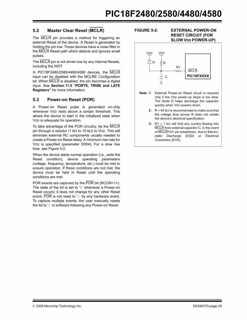
PIC18F2480/2580/4480/4580
5.2 Master Clear Reset (MCLR)The MCLR pin provides a method for triggering anexternal Reset of the device. A Reset is generated byholding the pin low. These devices have a noise filter inthe MCLR Reset path which detects and ignores smallpulses.The MCLR pin is not driven low by any internal Resets,including the WDT.
In PIC18F2480/2580/4480/4580 devices, the MCLRinput can be disabled with the MCLRE Configurationbit. When MCLR is disabled, the pin becomes a digitalinput. See Section 11.5 “PORTE, TRISE and LATERegisters” for more information.
5.3 Power-on Reset (POR)A Power-on Reset pulse is generated on-chipwhenever VDD rises above a certain threshold. Thisallows the device to start in the initialized state whenVDD is adequate for operation.
To take advantage of the POR circuitry, tie the MCLRpin through a resistor (1 kΩ to 10 kΩ) to VDD. This willeliminate external RC components usually needed tocreate a Power-on Reset delay. A minimum rise rate forVDD is specified (parameter D004). For a slow risetime, see Figure 5-2.
When the device starts normal operation (i.e., exits theReset condition), device operating parameters(voltage, frequency, temperature, etc.) must be met toensure operation. If these conditions are not met, thedevice must be held in Reset until the operatingconditions are met.
POR events are captured by the POR bit (RCON<1>).The state of the bit is set to ‘0’ whenever a Power-onReset occurs; it does not change for any other Resetevent. POR is not reset to ‘1’ by any hardware event.To capture multiple events, the user manually resetsthe bit to ‘1’ in software following any Power-on Reset.
FIGURE 5-2: EXTERNAL POWER-ON RESET CIRCUIT (FOR SLOW VDD POWER-UP)
Note 1: External Power-on Reset circuit is requiredonly if the VDD power-up slope is too slow.The diode D helps discharge the capacitorquickly when VDD powers down.
2: R < 40 kΩ is recommended to make sure thatthe voltage drop across R does not violatethe device’s electrical specification.
3: R1 ≥ 1 kΩ will limit any current flowing intoMCLR from external capacitor C, in the eventof MCLR/VPP pin breakdown, due to Electro-static Discharge (ESD) or ElectricalOverstress (EOS).
C
R1RD
VDD
MCLR
PIC18FXXXX
VDD
© 2009 Microchip Technology Inc. DS39637D-page 49

PIC18F2480/2580/4480/4580
5.4 Brown-out Reset (BOR)PIC18F2480/2580/4480/4580 devices implement aBOR circuit that provides the user with a number ofconfiguration and power-saving options. The BOR iscontrolled by the BORV<1:0> and BOREN<1:0>Configuration bits. There are a total of four BORconfigurations which are summarized in Table 5-1.The BOR threshold is set by the BORV<1:0> bits. IfBOR is enabled (any values of BOREN<1:0>, except‘00’), any drop of VDD below VBOR (parameter D005)for greater than TBOR (parameter 35) will reset thedevice. A Reset may or may not occur if VDD falls belowVBOR for less than TBOR. The chip will remain inBrown-out Reset until VDD rises above VBOR.
If the Power-up Timer is enabled, it will be invoked afterVDD rises above VBOR; it then will keep the chip inReset for an additional time delay, TPWRT(parameter 33). If VDD drops below VBOR while thePower-up Timer is running, the chip will go back into aBrown-out Reset and the Power-up Timer will beinitialized. Once VDD rises above VBOR, the Power-upTimer will execute the additional time delay.
BOR and the Power-on Timer (PWRT) areindependently configured. Enabling a Brown-out Resetdoes not automatically enable the PWRT.
5.4.1 SOFTWARE ENABLED BORWhen BOREN<1:0> = 01, the BOR can be enabled ordisabled by the user in software. This is done with thecontrol bit, SBOREN (RCON<6>). Setting SBORENenables the BOR to function as previously described.Clearing SBOREN disables the BOR entirely. TheSBOREN bit operates only in this mode; otherwise it isread as ‘0’.
Placing the BOR under software control gives the userthe additional flexibility of tailoring the application to itsenvironment without having to reprogram the device tochange BOR configuration. It also allows the user totailor device power consumption in software by elimi-nating the incremental current that the BOR consumes.While the BOR current is typically very small, it mayhave some impact in low-power applications.
5.4.2 DETECTING BORWhen Brown-out Reset is enabled, the BOR bit alwaysresets to ‘0’ on any Brown-out Reset or Power-onReset event. This makes it difficult to determine if aBrown-out Reset event has occurred just by readingthe state of BOR alone. A more reliable method is tosimultaneously check the state of both POR and BOR.This assumes that the POR bit is reset to ‘1’ in softwareimmediately after any Power-on Reset event. IF BORis ‘0’ while POR is ‘1’, it can be reliably assumed that aBrown-out Reset event has occurred.
5.4.3 DISABLING BOR IN SLEEP MODEWhen BOREN<1:0> = 10, the BOR remains underhardware control and operates as previouslydescribed. Whenever the device enters Sleep mode,however, the BOR is automatically disabled. When thedevice returns to any other operating mode, BOR isautomatically re-enabled.
This mode allows for applications to recover frombrown-out situations, while actively executing code,when the device requires BOR protection the most. Atthe same time, it saves additional power in Sleep modeby eliminating the small incremental BOR current.
TABLE 5-1: BOR CONFIGURATIONS
Note: Even when BOR is under software control,the Brown-out Reset voltage level is stillset by the BORV<1:0> Configuration bits.It cannot be changed in software.
BOR Configuration Status of SBOREN
(RCON<6>)BOR Operation
BOREN1 BOREN0
0 0 Unavailable BOR disabled; must be enabled by reprogramming the Configuration bits.0 1 Available BOR enabled in software; operation controlled by SBOREN.1 0 Unavailable BOR enabled in hardware in Run and Idle modes, disabled during Sleep
mode.1 1 Unavailable BOR enabled in hardware; must be disabled by reprogramming the
Configuration bits.
DS39637D-page 50 © 2009 Microchip Technology Inc.

PIC18F2480/2580/4480/4580
5.5 Device Reset TimersPIC18F2480/2580/4480/4580 devices incorporatethree separate on-chip timers that help regulate thePower-on Reset process. Their main function is toensure that the device clock is stable before code isexecuted. These timers are:• Power-up Timer (PWRT)• Oscillator Start-up Timer (OST)• PLL Lock Time-out
5.5.1 POWER-UP TIMER (PWRT)The Power-up Timer (PWRT) of the PIC18F2480/2580/4480/4580 devices is an 11-bit counter which uses theINTRC source as the clock input. This yields anapproximate time interval of 2048 x 32 μs = 65.6 ms.While the PWRT is counting, the device is held inReset.
The power-up time delay depends on the INTRC clockand will vary from chip-to-chip due to temperature andprocess variation. See DC parameter 33 for details.
The PWRT is enabled by clearing the PWRTENConfiguration bit.
5.5.2 OSCILLATOR START-UP TIMER (OST)
The Oscillator Start-up Timer (OST) provides a1024 oscillator cycle (from OSC1 input) delay after thePWRT delay is over (parameter 33). This ensures thatthe crystal oscillator or resonator has started andstabilized.
The OST time-out is invoked only for XT, LP, HS andHSPLL modes and only on Power-on Reset or on exitfrom most power-managed modes.
5.5.3 PLL LOCK TIME-OUTWith the PLL enabled in its PLL mode, the time-outsequence following a Power-on Reset is slightly differ-ent from other oscillator modes. A separate timer isused to provide a fixed time-out that is sufficient for thePLL to lock to the main oscillator frequency. This PLLlock time-out (TPLL) is typically 2 ms and follows theoscillator start-up time-out.
5.5.4 TIME-OUT SEQUENCEOn power-up, the time-out sequence is as follows:
1. After the POR pulse has cleared, PWRTtime-out is invoked (if enabled).
2. Then, the OST is activated.
The total time-out will vary based on oscillator configu-ration and the status of the PWRT. Figure 5-3,Figure 5-4, Figure 5-5, Figure 5-6 and Figure 5-7 alldepict time-out sequences on power-up, with thePower-up Timer enabled and the device operating inHS Oscillator mode. Figures 5-3 through 5-6 also applyto devices operating in XT or LP modes. For devices inRC mode and with the PWRT disabled, on the otherhand, there will be no time-out at all.
Since the time-outs occur from the POR pulse, if MCLRis kept low long enough, all time-outs will expire. Bring-ing MCLR high will begin execution immediately(Figure 5-5). This is useful for testing purposes or tosynchronize more than one PIC18FXXXX deviceoperating in parallel.
TABLE 5-2: TIME-OUT IN VARIOUS SITUATIONS
OscillatorConfiguration
Power-up(2) and Brown-out Exit from Power-Managed ModePWRTEN = 0 PWRTEN = 1
HSPLL 66 ms(1) + 1024 TOSC + 2 ms(2) 1024 TOSC + 2 ms(2) 1024 TOSC + 2 ms(2)
HS, XT, LP 66 ms(1) + 1024 TOSC 1024 TOSC 1024 TOSC
EC, ECIO 66 ms(1) — —RC, RCIO 66 ms(1) — —INTIO1, INTIO2 66 ms(1) — —Note 1: 66 ms (65.5 ms) is the nominal Power-up Timer (PWRT) delay.
2: 2 ms is the nominal time required for the PLL to lock.
© 2009 Microchip Technology Inc. DS39637D-page 51

PIC18F2480/2580/4480/4580
FIGURE 5-3: TIME-OUT SEQUENCE ON POWER-UP (MCLR TIED TO VDD, VDD RISE < TPWRT)FIGURE 5-4: TIME-OUT SEQUENCE ON POWER-UP (MCLR NOT TIED TO VDD): CASE 1
FIGURE 5-5: TIME-OUT SEQUENCE ON POWER-UP (MCLR NOT TIED TO VDD): CASE 2
TPWRT
TOST
VDD
MCLR
INTERNAL POR
PWRT TIME-OUT
OST TIME-OUT
INTERNAL RESET
TPWRT
TOST
VDD
MCLR
INTERNAL POR
PWRT TIME-OUT
OST TIME-OUT
INTERNAL RESET
VDD
MCLR
INTERNAL POR
PWRT TIME-OUT
OST TIME-OUT
INTERNAL RESET
TPWRT
TOST
DS39637D-page 52 © 2009 Microchip Technology Inc.
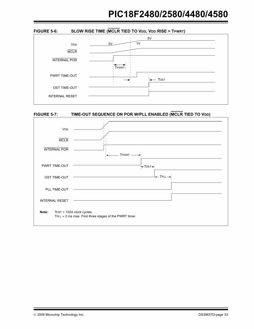
PIC18F2480/2580/4480/4580
FIGURE 5-6: SLOW RISE TIME (MCLR TIED TO VDD, VDD RISE > TPWRT)FIGURE 5-7: TIME-OUT SEQUENCE ON POR W/PLL ENABLED (MCLR TIED TO VDD)
VDD
MCLR
INTERNAL POR
PWRT TIME-OUT
OST TIME-OUT
INTERNAL RESET
0V 1V5V
TPWRT
TOST
TPWRT
TOST
VDD
MCLR
INTERNAL POR
PWRT TIME-OUT
OST TIME-OUT
INTERNAL RESET
PLL TIME-OUT
TPLL
Note: TOST = 1024 clock cycles.TPLL ≈ 2 ms max. First three stages of the PWRT timer.
© 2009 Microchip Technology Inc. DS39637D-page 53

PIC18F2480/2580/4480/4580
5.6 Reset State of RegistersMost registers are unaffected by a Reset. Their statusis unknown on a Power-on Reset and unchanged by allother Resets. The other registers are forced to a “Resetstate” depending on the type of Reset that occurred.Most registers are not affected by a WDT wake-up,since this is viewed as the resumption of normal oper-ation. Status bits from the RCON register, RI, TO, PD,POR and BOR, are set or cleared differently in different
Reset situations, as indicated in Table 5-3. These bitsare used in software to determine the nature of theReset.
Table 5-4 describes the Reset states for all of theSpecial Function Registers. These are categorized byPower-on and Brown-out Resets, Master Clear andWDT Resets and WDT wake-ups.
TABLE 5-3: STATUS BITS, THEIR SIGNIFICANCE AND THE INITIALIZATION CONDITION FOR RCON REGISTER
Condition Program Counter(1)
RCON Register STKPTR Register
SBOREN RI TO PD POR BOR STKFUL STKUNF
Power-on Reset 0000h 1 1 1 1 0 0 0 0
RESET Instruction 0000h u(2) 0 u u u u u u
Brown-out Reset 0000h u(2) 1 1 1 u 0 u u
MCLR Reset during Power-Managed Run modes
0000h u(2) u 1 u u u u u
MCLR Reset during Power-Managed Idle modes and Sleep mode
0000h u(2) u 1 0 u u u u
WDT Time-out during Full Power or Power-Managed Run modes
0000h u(2) u 0 u u u u u
MCLR Reset during Full-Power execution
0000h u(2) u u u u u u u
Stack Full Reset (STVREN = 1) 0000h u(2) u u u u u 1 u
Stack Underflow Reset (STVREN = 1)
0000h u(2) u u u u u u 1
Stack Underflow Error (not an actual Reset, STVREN = 0)
0000h u(2) u u u u u u 1
WDT Time-out during Power-Managed Idle or Sleep modes
PC + 2 u(2) u 0 0 u u u u
Interrupt Exit from Power-Managed modes
PC + 2 u(2) u u 0 u u u u
Legend: u = unchangedNote 1: When the wake-up is due to an interrupt and the GIEH or GIEL bits are set, the PC is loaded with the
interrupt vector (008h or 0018h).2: Reset state is ‘1’ for POR and unchanged for all other Resets when software BOR is enabled
(BOREN<1:0> Configuration bits = 01 and SBOREN = 1); otherwise, the Reset state is ‘0’.
DS39637D-page 54 © 2009 Microchip Technology Inc.
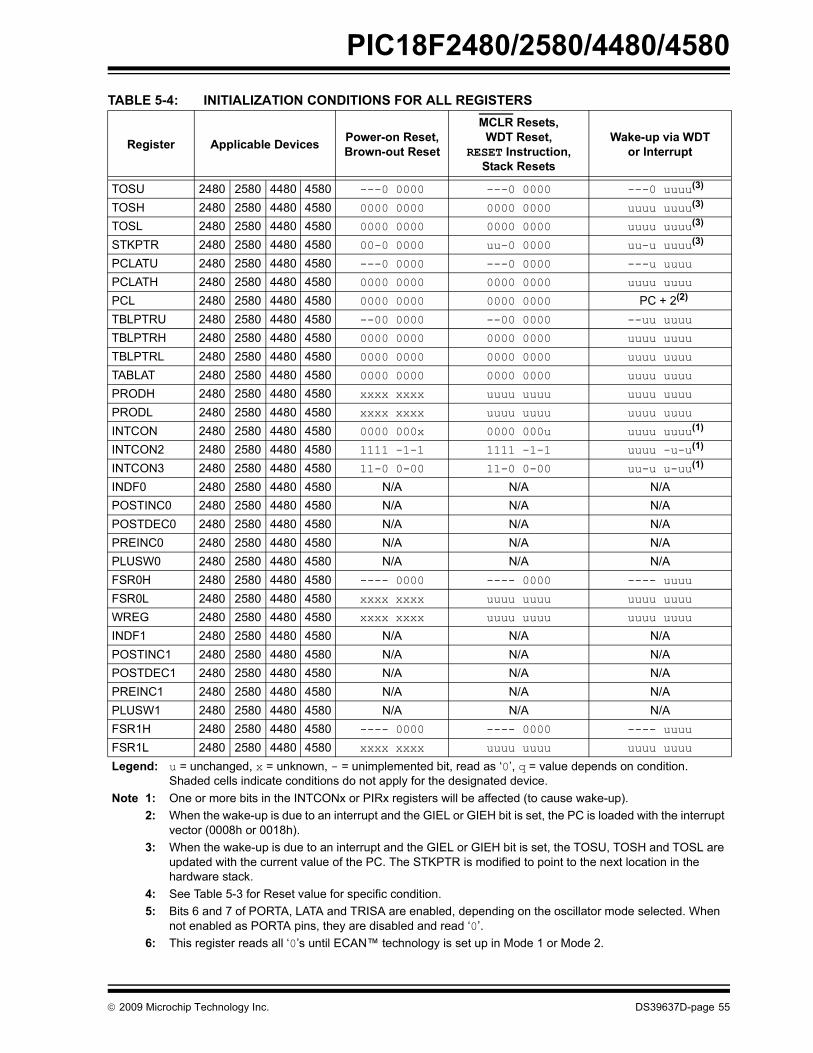
PIC18F2480/2580/4480/4580
TABLE 5-4: INITIALIZATION CONDITIONS FOR ALL REGISTERSRegister Applicable Devices Power-on Reset,Brown-out Reset
MCLR Resets,WDT Reset,
RESET Instruction,Stack Resets
Wake-up via WDT or Interrupt
TOSU 2480 2580 4480 4580 ---0 0000 ---0 0000 ---0 uuuu(3)
TOSH 2480 2580 4480 4580 0000 0000 0000 0000 uuuu uuuu(3)
TOSL 2480 2580 4480 4580 0000 0000 0000 0000 uuuu uuuu(3)
STKPTR 2480 2580 4480 4580 00-0 0000 uu-0 0000 uu-u uuuu(3)
PCLATU 2480 2580 4480 4580 ---0 0000 ---0 0000 ---u uuuu
PCLATH 2480 2580 4480 4580 0000 0000 0000 0000 uuuu uuuu
PCL 2480 2580 4480 4580 0000 0000 0000 0000 PC + 2(2)
TBLPTRU 2480 2580 4480 4580 --00 0000 --00 0000 --uu uuuu
TBLPTRH 2480 2580 4480 4580 0000 0000 0000 0000 uuuu uuuu
TBLPTRL 2480 2580 4480 4580 0000 0000 0000 0000 uuuu uuuu
TABLAT 2480 2580 4480 4580 0000 0000 0000 0000 uuuu uuuu
PRODH 2480 2580 4480 4580 xxxx xxxx uuuu uuuu uuuu uuuu
PRODL 2480 2580 4480 4580 xxxx xxxx uuuu uuuu uuuu uuuu
INTCON 2480 2580 4480 4580 0000 000x 0000 000u uuuu uuuu(1)
INTCON2 2480 2580 4480 4580 1111 -1-1 1111 -1-1 uuuu -u-u(1)
INTCON3 2480 2580 4480 4580 11-0 0-00 11-0 0-00 uu-u u-uu(1)
INDF0 2480 2580 4480 4580 N/A N/A N/APOSTINC0 2480 2580 4480 4580 N/A N/A N/APOSTDEC0 2480 2580 4480 4580 N/A N/A N/APREINC0 2480 2580 4480 4580 N/A N/A N/APLUSW0 2480 2580 4480 4580 N/A N/A N/AFSR0H 2480 2580 4480 4580 ---- 0000 ---- 0000 ---- uuuu
FSR0L 2480 2580 4480 4580 xxxx xxxx uuuu uuuu uuuu uuuu
WREG 2480 2580 4480 4580 xxxx xxxx uuuu uuuu uuuu uuuu
INDF1 2480 2580 4480 4580 N/A N/A N/APOSTINC1 2480 2580 4480 4580 N/A N/A N/APOSTDEC1 2480 2580 4480 4580 N/A N/A N/APREINC1 2480 2580 4480 4580 N/A N/A N/APLUSW1 2480 2580 4480 4580 N/A N/A N/AFSR1H 2480 2580 4480 4580 ---- 0000 ---- 0000 ---- uuuu
FSR1L 2480 2580 4480 4580 xxxx xxxx uuuu uuuu uuuu uuuu
Legend: u = unchanged, x = unknown, - = unimplemented bit, read as ‘0’, q = value depends on condition.Shaded cells indicate conditions do not apply for the designated device.
Note 1: One or more bits in the INTCONx or PIRx registers will be affected (to cause wake-up).2: When the wake-up is due to an interrupt and the GIEL or GIEH bit is set, the PC is loaded with the interrupt
vector (0008h or 0018h).3: When the wake-up is due to an interrupt and the GIEL or GIEH bit is set, the TOSU, TOSH and TOSL are
updated with the current value of the PC. The STKPTR is modified to point to the next location in the hardware stack.
4: See Table 5-3 for Reset value for specific condition.5: Bits 6 and 7 of PORTA, LATA and TRISA are enabled, depending on the oscillator mode selected. When
not enabled as PORTA pins, they are disabled and read ‘0’. 6: This register reads all ‘0’s until ECAN™ technology is set up in Mode 1 or Mode 2.
© 2009 Microchip Technology Inc. DS39637D-page 55

PIC18F2480/2580/4480/4580
BSR 2480 2580 4480 4580 ---- 0000 ---- 0000 ---- uuuu
INDF2 2480 2580 4480 4580 N/A N/A N/APOSTINC2 2480 2580 4480 4580 N/A N/A N/APOSTDEC2 2480 2580 4480 4580 N/A N/A N/APREINC2 2480 2580 4480 4580 N/A N/A N/APLUSW2 2480 2580 4480 4580 N/A N/A N/AFSR2H 2480 2580 4480 4580 ---- 0000 ---- 0000 ---- uuuu
FSR2L 2480 2580 4480 4580 xxxx xxxx uuuu uuuu uuuu uuuu
STATUS 2480 2580 4480 4580 ---x xxxx ---u uuuu ---u uuuu
TMR0H 2480 2580 4480 4580 0000 0000 0000 0000 uuuu uuuu
TMR0L 2480 2580 4480 4580 xxxx xxxx uuuu uuuu uuuu uuuu
T0CON 2480 2580 4480 4580 1111 1111 1111 1111 uuuu uuuu
OSCCON 2480 2580 4480 4580 0100 q000 0100 00q0 uuuu uuqu
HLVDCON 2480 2580 4480 4580 0-00 0101 0-00 0101 0-uu uuuu
WDTCON 2480 2580 4480 4580 ---- ---0 ---- ---0 ---- ---u
RCON(4) 2480 2580 4480 4580 0q-1 11q0 0q-q qquu uq-u qquu
TMR1H 2480 2580 4480 4580 xxxx xxxx uuuu uuuu uuuu uuuu
TMR1L 2480 2580 4480 4580 xxxx xxxx uuuu uuuu uuuu uuuu
T1CON 2480 2580 4480 4580 0000 0000 u0uu uuuu uuuu uuuu
TMR2 2480 2580 4480 4580 0000 0000 0000 0000 uuuu uuuu
PR2 2480 2580 4480 4580 1111 1111 1111 1111 1111 1111
T2CON 2480 2580 4480 4580 -000 0000 -000 0000 -uuu uuuu
SSPBUF 2480 2580 4480 4580 xxxx xxxx uuuu uuuu uuuu uuuu
SSPADD 2480 2580 4480 4580 0000 0000 0000 0000 uuuu uuuu
SSPSTAT 2480 2580 4480 4580 0000 0000 0000 0000 uuuu uuuu
SSPCON1 2480 2580 4480 4580 0000 0000 0000 0000 uuuu uuuu
SSPCON2 2480 2580 4480 4580 0000 0000 0000 0000 uuuu uuuu
ADRESH 2480 2580 4480 4580 xxxx xxxx uuuu uuuu uuuu uuuu
ADRESL 2480 2580 4480 4580 xxxx xxxx uuuu uuuu uuuu uuuu
ADCON0 2480 2580 4480 4580 --00 0000 --00 0000 --uu uuuu
ADCON1 2480 2580 4480 4580 --00 0qqq --00 0qqq --uu uuuu
TABLE 5-4: INITIALIZATION CONDITIONS FOR ALL REGISTERS (CONTINUED)
Register Applicable Devices Power-on Reset,Brown-out Reset
MCLR Resets,WDT Reset,
RESET Instruction,Stack Resets
Wake-up via WDT or Interrupt
Legend: u = unchanged, x = unknown, - = unimplemented bit, read as ‘0’, q = value depends on condition.Shaded cells indicate conditions do not apply for the designated device.
Note 1: One or more bits in the INTCONx or PIRx registers will be affected (to cause wake-up).2: When the wake-up is due to an interrupt and the GIEL or GIEH bit is set, the PC is loaded with the interrupt
vector (0008h or 0018h).3: When the wake-up is due to an interrupt and the GIEL or GIEH bit is set, the TOSU, TOSH and TOSL are
updated with the current value of the PC. The STKPTR is modified to point to the next location in the hardware stack.
4: See Table 5-3 for Reset value for specific condition.5: Bits 6 and 7 of PORTA, LATA and TRISA are enabled, depending on the oscillator mode selected. When
not enabled as PORTA pins, they are disabled and read ‘0’. 6: This register reads all ‘0’s until ECAN™ technology is set up in Mode 1 or Mode 2.
DS39637D-page 56 © 2009 Microchip Technology Inc.
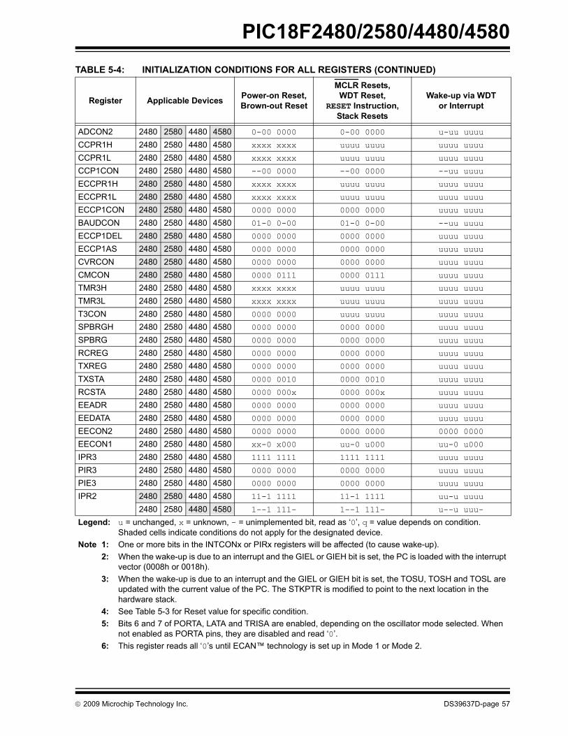
PIC18F2480/2580/4480/4580
ADCON2 2480 2580 4480 4580 0-00 0000 0-00 0000 u-uu uuuu
CCPR1H 2480 2580 4480 4580 xxxx xxxx uuuu uuuu uuuu uuuu
CCPR1L 2480 2580 4480 4580 xxxx xxxx uuuu uuuu uuuu uuuu
CCP1CON 2480 2580 4480 4580 --00 0000 --00 0000 --uu uuuu
ECCPR1H 2480 2580 4480 4580 xxxx xxxx uuuu uuuu uuuu uuuu
ECCPR1L 2480 2580 4480 4580 xxxx xxxx uuuu uuuu uuuu uuuu
ECCP1CON 2480 2580 4480 4580 0000 0000 0000 0000 uuuu uuuu
BAUDCON 2480 2580 4480 4580 01-0 0-00 01-0 0-00 --uu uuuu
ECCP1DEL 2480 2580 4480 4580 0000 0000 0000 0000 uuuu uuuu
ECCP1AS 2480 2580 4480 4580 0000 0000 0000 0000 uuuu uuuu
CVRCON 2480 2580 4480 4580 0000 0000 0000 0000 uuuu uuuu
CMCON 2480 2580 4480 4580 0000 0111 0000 0111 uuuu uuuu
TMR3H 2480 2580 4480 4580 xxxx xxxx uuuu uuuu uuuu uuuu
TMR3L 2480 2580 4480 4580 xxxx xxxx uuuu uuuu uuuu uuuu
T3CON 2480 2580 4480 4580 0000 0000 uuuu uuuu uuuu uuuu
SPBRGH 2480 2580 4480 4580 0000 0000 0000 0000 uuuu uuuu
SPBRG 2480 2580 4480 4580 0000 0000 0000 0000 uuuu uuuu
RCREG 2480 2580 4480 4580 0000 0000 0000 0000 uuuu uuuu
TXREG 2480 2580 4480 4580 0000 0000 0000 0000 uuuu uuuu
TXSTA 2480 2580 4480 4580 0000 0010 0000 0010 uuuu uuuu
RCSTA 2480 2580 4480 4580 0000 000x 0000 000x uuuu uuuu
EEADR 2480 2580 4480 4580 0000 0000 0000 0000 uuuu uuuu
EEDATA 2480 2580 4480 4580 0000 0000 0000 0000 uuuu uuuu
EECON2 2480 2580 4480 4580 0000 0000 0000 0000 0000 0000
EECON1 2480 2580 4480 4580 xx-0 x000 uu-0 u000 uu-0 u000
IPR3 2480 2580 4480 4580 1111 1111 1111 1111 uuuu uuuu
PIR3 2480 2580 4480 4580 0000 0000 0000 0000 uuuu uuuu
PIE3 2480 2580 4480 4580 0000 0000 0000 0000 uuuu uuuu
IPR2 2480 2580 4480 4580 11-1 1111 11-1 1111 uu-u uuuu
2480 2580 4480 4580 1--1 111- 1--1 111- u--u uuu-
TABLE 5-4: INITIALIZATION CONDITIONS FOR ALL REGISTERS (CONTINUED)
Register Applicable Devices Power-on Reset,Brown-out Reset
MCLR Resets,WDT Reset,
RESET Instruction,Stack Resets
Wake-up via WDT or Interrupt
Legend: u = unchanged, x = unknown, - = unimplemented bit, read as ‘0’, q = value depends on condition.Shaded cells indicate conditions do not apply for the designated device.
Note 1: One or more bits in the INTCONx or PIRx registers will be affected (to cause wake-up).2: When the wake-up is due to an interrupt and the GIEL or GIEH bit is set, the PC is loaded with the interrupt
vector (0008h or 0018h).3: When the wake-up is due to an interrupt and the GIEL or GIEH bit is set, the TOSU, TOSH and TOSL are
updated with the current value of the PC. The STKPTR is modified to point to the next location in the hardware stack.
4: See Table 5-3 for Reset value for specific condition.5: Bits 6 and 7 of PORTA, LATA and TRISA are enabled, depending on the oscillator mode selected. When
not enabled as PORTA pins, they are disabled and read ‘0’. 6: This register reads all ‘0’s until ECAN™ technology is set up in Mode 1 or Mode 2.
© 2009 Microchip Technology Inc. DS39637D-page 57

PIC18F2480/2580/4480/4580
PIR2 2480 2580 4480 4580 00-0 0000 00-0 0000 uu-u uuuu(1)
2480 2580 4480 4580 0--0 000- 0--0 000- u--u uuu-(1)
PIE2 2480 2580 4480 4580 00-0 0000 00-0 0000 uu-u uuuu
2480 2580 4480 4580 0--0 000- 0--0 000- u--u uuu-
IPR1 2480 2580 4480 4580 1111 1111 1111 1111 uuuu uuuu
2480 2580 4480 4580 -111 1111 -111 1111 -uuu uuuu
PIR1 2480 2580 4480 4580 0000 0000 0000 0000 uuuu uuuu(1)
2480 2580 4480 4580 -000 0000 -000 0000 -uuu uuuu
PIE1 2480 2580 4480 4580 0000 0000 0000 0000 uuuu uuuu
2480 2580 4480 4580 -000 0000 -000 0000 -uuu uuuu
OSCTUNE 2480 2580 4480 4580 --00 0000 --00 0000 --uu uuuu
TRISE 2480 2580 4480 4580 0000 -111 0000 -111 uuuu -uuu
TRISD 2480 2580 4480 4580 1111 1111 1111 1111 uuuu uuuu
TRISC 2480 2580 4480 4580 1111 1111 1111 1111 uuuu uuuu
TRISB 2480 2580 4480 4580 1111 1111 1111 1111 uuuu uuuu
TRISA(5) 2480 2580 4480 4580 1111 1111(5) 1111 1111(5) uuuu uuuu(5)
LATE 2480 2580 4480 4580 ---- -xxx ---- -uuu ---- -uuu
LATD 2480 2580 4480 4580 xxxx xxxx uuuu uuuu uuuu uuuu
LATC 2480 2580 4480 4580 xxxx xxxx uuuu uuuu uuuu uuuu
LATB 2480 2580 4480 4580 xxxx xxxx uuuu uuuu uuuu uuuu
LATA(5) 2480 2580 4480 4580 xxxx xxxx(5) uuuu uuuu(5) uuuu uuuu(5)
PORTE 2480 2580 4480 4580 ---- x000 ---- x000 ---- uuuu
PORTD 2480 2580 4480 4580 xxxx xxxx uuuu uuuu uuuu uuuu
PORTC 2480 2580 4480 4580 xxxx xxxx uuuu uuuu uuuu uuuu
PORTB 2480 2580 4480 4580 xxxx xxxx uuuu uuuu uuuu uuuu
PORTA(5) 2480 2580 4480 4580 xx0x 0000(5) uu0u 0000(5) uuuu uuuu(5)
ECANCON 2480 2580 4480 4580 0001 0000 0001 0000 uuuu uuuu
TXERRCNT 2480 2580 4480 4580 0000 0000 0000 0000 uuuu uuuu
RXERRCNT 2480 2580 4480 4580 0000 0000 0000 0000 uuuu uuuu
COMSTAT 2480 2580 4480 4580 0000 0000 0000 0000 uuuu uuuu
CIOCON 2480 2580 4480 4580 --00 ---- --00 ---- --uu ----
TABLE 5-4: INITIALIZATION CONDITIONS FOR ALL REGISTERS (CONTINUED)
Register Applicable Devices Power-on Reset,Brown-out Reset
MCLR Resets,WDT Reset,
RESET Instruction,Stack Resets
Wake-up via WDT or Interrupt
Legend: u = unchanged, x = unknown, - = unimplemented bit, read as ‘0’, q = value depends on condition.Shaded cells indicate conditions do not apply for the designated device.
Note 1: One or more bits in the INTCONx or PIRx registers will be affected (to cause wake-up).2: When the wake-up is due to an interrupt and the GIEL or GIEH bit is set, the PC is loaded with the interrupt
vector (0008h or 0018h).3: When the wake-up is due to an interrupt and the GIEL or GIEH bit is set, the TOSU, TOSH and TOSL are
updated with the current value of the PC. The STKPTR is modified to point to the next location in the hardware stack.
4: See Table 5-3 for Reset value for specific condition.5: Bits 6 and 7 of PORTA, LATA and TRISA are enabled, depending on the oscillator mode selected. When
not enabled as PORTA pins, they are disabled and read ‘0’. 6: This register reads all ‘0’s until ECAN™ technology is set up in Mode 1 or Mode 2.
DS39637D-page 58 © 2009 Microchip Technology Inc.

PIC18F2480/2580/4480/4580
BRGCON3 2480 2580 4480 4580 00-- -000 00-- -000 uu-- -uuu
BRGCON2 2480 2580 4480 4580 0000 0000 0000 0000 uuuu uuuu
BRGCON1 2480 2580 4480 4580 0000 0000 0000 0000 uuuu uuuu
CANCON 2480 2580 4480 4580 1000 000- 1000 000- uuuu uuu-
CANSTAT 2480 2580 4480 4580 100- 000- 100- 000- uuu- uuu-
RXB0D7 2480 2580 4480 4580 xxxx xxxx uuuu uuuu uuuu uuuu
RXB0D6 2480 2580 4480 4580 xxxx xxxx uuuu uuuu uuuu uuuu
RXB0D5 2480 2580 4480 4580 xxxx xxxx uuuu uuuu uuuu uuuu
RXB0D4 2480 2580 4480 4580 xxxx xxxx uuuu uuuu uuuu uuuu
RXB0D3 2480 2580 4480 4580 xxxx xxxx uuuu uuuu uuuu uuuu
RXB0D2 2480 2580 4480 4580 xxxx xxxx uuuu uuuu uuuu uuuu
RXB0D1 2480 2580 4480 4580 xxxx xxxx uuuu uuuu uuuu uuuu
RXB0D0 2480 2580 4480 4580 xxxx xxxx uuuu uuuu uuuu uuuu
RXB0DLC 2480 2580 4480 4580 -xxx xxxx -uuu uuuu -uuu uuuu
RXB0EIDL 2480 2580 4480 4580 xxxx xxxx uuuu uuuu uuuu uuuu
RXB0EIDH 2480 2580 4480 4580 xxxx xxxx uuuu uuuu uuuu uuuu
RXB0SIDL 2480 2580 4480 4580 xxxx x-xx uuuu u-uu uuuu u-uu
RXB0SIDH 2480 2580 4480 4580 xxxx xxxx uuuu uuuu uuuu uuuu
RXB0CON 2480 2580 4480 4580 000- 0000 000- 0000 uuu- uuuu
RXB1D7 2480 2580 4480 4580 xxxx xxxx uuuu uuuu uuuu uuuu
RXB1D6 2480 2580 4480 4580 xxxx xxxx uuuu uuuu uuuu uuuu
RXB1D5 2480 2580 4480 4580 xxxx xxxx uuuu uuuu uuuu uuuu
RXB1D4 2480 2580 4480 4580 xxxx xxxx uuuu uuuu uuuu uuuu
RXB1D3 2480 2580 4480 4580 xxxx xxxx uuuu uuuu uuuu uuuu
RXB1D2 2480 2580 4480 4580 xxxx xxxx uuuu uuuu uuuu uuuu
RXB1D1 2480 2580 4480 4580 xxxx xxxx uuuu uuuu uuuu uuuu
RXB1D0 2480 2580 4480 4580 xxxx xxxx uuuu uuuu uuuu uuuu
RXB1DLC 2480 2580 4480 4580 -xxx xxxx -uuu uuuu -uuu uuuu
RXB1EIDL 2480 2580 4480 4580 xxxx xxxx uuuu uuuu uuuu uuuu
RXB1EIDH 2480 2580 4480 4580 xxxx xxxx uuuu uuuu uuuu uuuu
RXB1SIDL 2480 2580 4480 4580 xxxx x-xx uuuu u-uu uuuu u-uu
TABLE 5-4: INITIALIZATION CONDITIONS FOR ALL REGISTERS (CONTINUED)
Register Applicable Devices Power-on Reset,Brown-out Reset
MCLR Resets,WDT Reset,
RESET Instruction,Stack Resets
Wake-up via WDT or Interrupt
Legend: u = unchanged, x = unknown, - = unimplemented bit, read as ‘0’, q = value depends on condition.Shaded cells indicate conditions do not apply for the designated device.
Note 1: One or more bits in the INTCONx or PIRx registers will be affected (to cause wake-up).2: When the wake-up is due to an interrupt and the GIEL or GIEH bit is set, the PC is loaded with the interrupt
vector (0008h or 0018h).3: When the wake-up is due to an interrupt and the GIEL or GIEH bit is set, the TOSU, TOSH and TOSL are
updated with the current value of the PC. The STKPTR is modified to point to the next location in the hardware stack.
4: See Table 5-3 for Reset value for specific condition.5: Bits 6 and 7 of PORTA, LATA and TRISA are enabled, depending on the oscillator mode selected. When
not enabled as PORTA pins, they are disabled and read ‘0’. 6: This register reads all ‘0’s until ECAN™ technology is set up in Mode 1 or Mode 2.
© 2009 Microchip Technology Inc. DS39637D-page 59

PIC18F2480/2580/4480/4580
RXB1SIDH 2480 2580 4480 4580 xxxx xxxx uuuu uuuu uuuu uuuu
RXB1CON 2480 2580 4480 4580 000- 0000 000- 0000 uuu- uuuu
TXB0D7 2480 2580 4480 4580 xxxx xxxx uuuu uuuu uuuu uuuu
TXB0D6 2480 2580 4480 4580 xxxx xxxx uuuu uuuu uuuu uuuu
TXB0D5 2480 2580 4480 4580 xxxx xxxx uuuu uuuu uuuu uuuu
TXB0D4 2480 2580 4480 4580 xxxx xxxx uuuu uuuu uuuu uuuu
TXB0D3 2480 2580 4480 4580 xxxx xxxx uuuu uuuu uuuu uuuu
TXB0D2 2480 2580 4480 4580 xxxx xxxx uuuu uuuu uuuu uuuu
TXB0D1 2480 2580 4480 4580 xxxx xxxx uuuu uuuu uuuu uuuu
TXB0D0 2480 2580 4480 4580 xxxx xxxx uuuu uuuu uuuu uuuu
TXB0DLC 2480 2580 4480 4580 -x-- xxxx -u-- uuuu -u-- uuuu
TXB0EIDL 2480 2580 4480 4580 xxxx xxxx uuuu uuuu uuuu uuuu
TXB0EIDH 2480 2580 4480 4580 xxxx xxxx uuuu uuuu -uuu uuuu
TXB0SIDL 2480 2580 4480 4580 xxx- x-xx uuu- u-uu uuu- u-uu
TXB0SIDH 2480 2580 4480 4580 xxxx xxxx uuuu uuuu uuuu uuuu
TXB0CON 2480 2580 4480 4580 0000 0-00 0000 0-00 uuuu u-uu
TXB1D7 2480 2580 4480 4580 xxxx xxxx uuuu uuuu uuuu uuuu
TXB1D6 2480 2580 4480 4580 xxxx xxxx uuuu uuuu uuuu uuuu
TXB1D5 2480 2580 4480 4580 xxxx xxxx uuuu uuuu uuuu uuuu
TXB1D4 2480 2580 4480 4580 xxxx xxxx uuuu uuuu uuuu uuuu
TXB1D3 2480 2580 4480 4580 xxxx xxxx uuuu uuuu uuuu uuuu
TXB1D2 2480 2580 4480 4580 xxxx xxxx uuuu uuuu uuuu uuuu
TXB1D1 2480 2580 4480 4580 xxxx xxxx uuuu uuuu uuuu uuuu
TXB1D0 2480 2580 4480 4580 xxxx xxxx uuuu uuuu uuuu uuuu
TXB1DLC 2480 2580 4480 4580 -x-- xxxx -u-- uuuu -u-- uuuu
TXB1EIDL 2480 2580 4480 4580 xxxx xxxx uuuu uuuu uuuu uuuu
TXB1EIDH 2480 2580 4480 4580 xxxx xxxx uuuu uuuu uuuu uuuu
TXB1SIDL 2480 2580 4480 4580 xxx- x-xx uuu- u-uu uuu- uu-u
TXB1SIDH 2480 2580 4480 4580 xxxx xxxx uuuu uuuu -uuu uuuu
TXB1CON 2480 2580 4480 4580 0000 0-00 0000 0-00 uuuu u-uu
TXB2D7 2480 2580 4480 4580 xxxx xxxx uuuu uuuu 0uuu uuuu
TABLE 5-4: INITIALIZATION CONDITIONS FOR ALL REGISTERS (CONTINUED)
Register Applicable Devices Power-on Reset,Brown-out Reset
MCLR Resets,WDT Reset,
RESET Instruction,Stack Resets
Wake-up via WDT or Interrupt
Legend: u = unchanged, x = unknown, - = unimplemented bit, read as ‘0’, q = value depends on condition.Shaded cells indicate conditions do not apply for the designated device.
Note 1: One or more bits in the INTCONx or PIRx registers will be affected (to cause wake-up).2: When the wake-up is due to an interrupt and the GIEL or GIEH bit is set, the PC is loaded with the interrupt
vector (0008h or 0018h).3: When the wake-up is due to an interrupt and the GIEL or GIEH bit is set, the TOSU, TOSH and TOSL are
updated with the current value of the PC. The STKPTR is modified to point to the next location in the hardware stack.
4: See Table 5-3 for Reset value for specific condition.5: Bits 6 and 7 of PORTA, LATA and TRISA are enabled, depending on the oscillator mode selected. When
not enabled as PORTA pins, they are disabled and read ‘0’. 6: This register reads all ‘0’s until ECAN™ technology is set up in Mode 1 or Mode 2.
DS39637D-page 60 © 2009 Microchip Technology Inc.

PIC18F2480/2580/4480/4580
TXB2D6 2480 2580 4480 4580 xxxx xxxx uuuu uuuu 0uuu uuuu
TXB2D5 2480 2580 4480 4580 xxxx xxxx uuuu uuuu 0uuu uuuu
TXB2D4 2480 2580 4480 4580 xxxx xxxx uuuu uuuu 0uuu uuuu
TXB2D3 2480 2580 4480 4580 xxxx xxxx uuuu uuuu 0uuu uuuu
TXB2D2 2480 2580 4480 4580 xxxx xxxx uuuu uuuu 0uuu uuuu
TXB2D1 2480 2580 4480 4580 xxxx xxxx uuuu uuuu 0uuu uuuu
TXB2D0 2480 2580 4480 4580 xxxx xxxx uuuu uuuu 0uuu uuuu
TXB2DLC 2480 2580 4480 4580 -x-- xxxx -u-- uuuu -u-- uuuu
TXB2EIDL 2480 2580 4480 4580 xxxx xxxx uuuu uuuu uuuu uuuu
TXB2EIDH 2480 2580 4480 4580 xxxx xxxx uuuu uuuu uuuu uuuu
TXB2SIDL 2480 2580 4480 4580 xxxx x-xx uuuu u-uu -uuu uuuu
TXB2SIDH 2480 2580 4480 4580 xxx- x-xx uuu- u-uu uuu- u-uu
TXB2CON 2480 2580 4480 4580 0000 0-00 0000 0-00 uuuu u-uu
RXM1EIDL 2480 2580 4480 4580 xxxx xxxx uuuu uuuu uuuu uuuu
RXM1EIDH 2480 2580 4480 4580 xxxx xxxx uuuu uuuu uuuu uuuu
RXM1SIDL 2480 2580 4480 4580 xxx- x-xx uuu- u-uu uuu- u-uu
RXM1SIDH 2480 2580 4480 4580 xxxx xxxx uuuu uuuu uuuu uuuu
RXM0EIDL 2480 2580 4480 4580 xxxx xxxx uuuu uuuu uuuu uuuu
RXM0EIDH 2480 2580 4480 4580 xxxx xxxx uuuu uuuu uuuu uuuu
RXM0SIDL 2480 2580 4480 4580 xxx- x-xx uuu- u-uu uuu- u-uu
RXM0SIDH 2480 2580 4480 4580 xxxx xxxx uuuu uuuu uuuu uuuu
RXF5EIDL 2480 2580 4480 4580 xxxx xxxx uuuu uuuu uuuu uuuu
RXF5EIDH 2480 2580 4480 4580 xxxx xxxx uuuu uuuu uuuu uuuu
RXF5SIDL 2480 2580 4480 4580 xxx- x-xx uuu- u-uu uuu- u-uu
RXF5SIDH 2480 2580 4480 4580 xxxx xxxx uuuu uuuu uuuu uuuu
RXF4EIDL 2480 2580 4480 4580 xxxx xxxx uuuu uuuu uuuu uuuu
RXF4EIDH 2480 2580 4480 4580 xxxx xxxx uuuu uuuu uuuu uuuu
RXF4SIDL 2480 2580 4480 4580 xxx- x-xx uuu- u-uu uuu- u-uu
RXF4SIDH 2480 2580 4480 4580 xxxx xxxx uuuu uuuu uuuu uuuu
RXF3EIDL 2480 2580 4480 4580 xxxx xxxx uuuu uuuu uuuu uuuu
RXF3EIDH 2480 2580 4480 4580 xxxx xxxx uuuu uuuu uuuu uuuu
TABLE 5-4: INITIALIZATION CONDITIONS FOR ALL REGISTERS (CONTINUED)
Register Applicable Devices Power-on Reset,Brown-out Reset
MCLR Resets,WDT Reset,
RESET Instruction,Stack Resets
Wake-up via WDT or Interrupt
Legend: u = unchanged, x = unknown, - = unimplemented bit, read as ‘0’, q = value depends on condition.Shaded cells indicate conditions do not apply for the designated device.
Note 1: One or more bits in the INTCONx or PIRx registers will be affected (to cause wake-up).2: When the wake-up is due to an interrupt and the GIEL or GIEH bit is set, the PC is loaded with the interrupt
vector (0008h or 0018h).3: When the wake-up is due to an interrupt and the GIEL or GIEH bit is set, the TOSU, TOSH and TOSL are
updated with the current value of the PC. The STKPTR is modified to point to the next location in the hardware stack.
4: See Table 5-3 for Reset value for specific condition.5: Bits 6 and 7 of PORTA, LATA and TRISA are enabled, depending on the oscillator mode selected. When
not enabled as PORTA pins, they are disabled and read ‘0’. 6: This register reads all ‘0’s until ECAN™ technology is set up in Mode 1 or Mode 2.
© 2009 Microchip Technology Inc. DS39637D-page 61

PIC18F2480/2580/4480/4580
RXF3SIDL 2480 2580 4480 4580 xxx- x-xx uuu- u-uu uuu- u-uu
RXF3SIDH 2480 2580 4480 4580 xxxx xxxx uuuu uuuu uuuu uuuu
RXF2EIDL 2480 2580 4480 4580 xxxx xxxx uuuu uuuu uuuu uuuu
RXF2EIDH 2480 2580 4480 4580 xxxx xxxx uuuu uuuu uuuu uuuu
RXF2SIDL 2480 2580 4480 4580 xxx- x-xx uuu- u-uu uuu- u-uu
RXF2SIDH 2480 2580 4480 4580 xxxx xxxx uuuu uuuu uuuu uuuu
RXF1EIDL 2480 2580 4480 4580 xxxx xxxx uuuu uuuu uuuu uuuu
RXF1EIDH 2480 2580 4480 4580 xxxx xxxx uuuu uuuu uuuu uuuu
RXF1SIDL 2480 2580 4480 4580 xxx- x-xx uuu- u-uu uuu- u-uu
RXF1SIDH 2480 2580 4480 4580 xxxx xxxx uuuu uuuu uuuu uuuu
RXF0EIDL 2480 2580 4480 4580 xxxx xxxx uuuu uuuu uuuu uuuu
RXF0EIDH 2480 2580 4480 4580 xxxx xxxx uuuu uuuu uuuu uuuu
RXF0SIDL 2480 2580 4480 4580 xxx- x-xx uuu- u-uu uuu- u-uu
RXF0SIDH 2480 2580 4480 4580 xxxx xxxx uuuu uuuu uuuu uuuu
B5D7(6) 2480 2580 4480 4580 xxxx xxxx uuuu uuuu uuuu uuuu
B5D6(6) 2480 2580 4480 4580 xxxx xxxx uuuu uuuu uuuu uuuu
B5D5(6) 2480 2580 4480 4580 xxxx xxxx uuuu uuuu uuuu uuuu
B5D4(6) 2480 2580 4480 4580 xxxx xxxx uuuu uuuu uuuu uuuu
B5D3(6) 2480 2580 4480 4580 xxxx xxxx uuuu uuuu uuuu uuuu
B5D2(6) 2480 2580 4480 4580 xxxx xxxx uuuu uuuu uuuu uuuu
B5D1(6) 2480 2580 4480 4580 xxxx xxxx uuuu uuuu uuuu uuuu
B5D0(6) 2480 2580 4480 4580 xxxx xxxx uuuu uuuu uuuu uuuu
B5DLC(6) 2480 2580 4480 4580 -xxx xxxx -uuu uuuu -uuu uuuu
B5EIDL(6) 2480 2580 4480 4580 xxxx xxxx uuuu uuuu uuuu uuuu
B5EIDH(6) 2480 2580 4480 4580 xxxx xxxx uuuu uuuu uuuu uuuu
B5SIDL(6) 2480 2580 4480 4580 xxxx x-xx uuuu u-uu uuuu u-uu
B5SIDH(6) 2480 2580 4480 4580 xxxx x-xx uuuu u-uu uuuu u-uu
B5CON(6) 2480 2580 4480 4580 0000 0000 0000 0000 uuuu uuuu
B4D7(6) 2480 2580 4480 4580 xxxx xxxx uuuu uuuu uuuu uuuu
B4D6(6) 2480 2580 4480 4580 xxxx xxxx uuuu uuuu uuuu uuuu
B4D5(6) 2480 2580 4480 4580 xxxx xxxx uuuu uuuu uuuu uuuu
TABLE 5-4: INITIALIZATION CONDITIONS FOR ALL REGISTERS (CONTINUED)
Register Applicable Devices Power-on Reset,Brown-out Reset
MCLR Resets,WDT Reset,
RESET Instruction,Stack Resets
Wake-up via WDT or Interrupt
Legend: u = unchanged, x = unknown, - = unimplemented bit, read as ‘0’, q = value depends on condition.Shaded cells indicate conditions do not apply for the designated device.
Note 1: One or more bits in the INTCONx or PIRx registers will be affected (to cause wake-up).2: When the wake-up is due to an interrupt and the GIEL or GIEH bit is set, the PC is loaded with the interrupt
vector (0008h or 0018h).3: When the wake-up is due to an interrupt and the GIEL or GIEH bit is set, the TOSU, TOSH and TOSL are
updated with the current value of the PC. The STKPTR is modified to point to the next location in the hardware stack.
4: See Table 5-3 for Reset value for specific condition.5: Bits 6 and 7 of PORTA, LATA and TRISA are enabled, depending on the oscillator mode selected. When
not enabled as PORTA pins, they are disabled and read ‘0’. 6: This register reads all ‘0’s until ECAN™ technology is set up in Mode 1 or Mode 2.
DS39637D-page 62 © 2009 Microchip Technology Inc.

PIC18F2480/2580/4480/4580
B4D4(6) 2480 2580 4480 4580 xxxx xxxx uuuu uuuu uuuu uuuu
B4D3(6) 2480 2580 4480 4580 xxxx xxxx uuuu uuuu uuuu uuuu
B4D2(6) 2480 2580 4480 4580 xxxx xxxx uuuu uuuu uuuu uuuu
B4D1(6) 2480 2580 4480 4580 xxxx xxxx uuuu uuuu uuuu uuuu
B4D0(6) 2480 2580 4480 4580 xxxx xxxx uuuu uuuu uuuu uuuu
B4DLC(6) 2480 2580 4480 4580 -xxx xxxx -uuu uuuu -uuu uuuu
B4EIDL(6) 2480 2580 4480 4580 xxxx xxxx uuuu uuuu uuuu uuuu
B4EIDH(6) 2480 2580 4480 4580 xxxx xxxx uuuu uuuu uuuu uuuu
B4SIDL(6) 2480 2580 4480 4580 xxxx x-xx uuuu u-uu uuuu u-uu
B4SIDH(6) 2480 2580 4480 4580 xxxx xxxx uuuu uuuu uuuu uuuu
B4CON(6) 2480 2580 4480 4580 0000 0000 0000 0000 uuuu uuuu
B3D7(6) 2480 2580 4480 4580 xxxx xxxx uuuu uuuu uuuu uuuu
B3D6(6) 2480 2580 4480 4580 xxxx xxxx uuuu uuuu uuuu uuuu
B3D5(6) 2480 2580 4480 4580 xxxx xxxx uuuu uuuu uuuu uuuu
B3D4(6) 2480 2580 4480 4580 xxxx xxxx uuuu uuuu uuuu uuuu
B3D3(6) 2480 2580 4480 4580 xxxx xxxx uuuu uuuu uuuu uuuu
B3D2(6) 2480 2580 4480 4580 xxxx xxxx uuuu uuuu uuuu uuuu
B3D1(6) 2480 2580 4480 4580 xxxx xxxx uuuu uuuu uuuu uuuu
B3D0(6) 2480 2580 4480 4580 xxxx xxxx uuuu uuuu uuuu uuuu
B3DLC(6) 2480 2580 4480 4580 -xxx xxxx -uuu uuuu -uuu uuuu
B3EIDL(6) 2480 2580 4480 4580 xxxx xxxx uuuu uuuu uuuu uuuu
B3EIDH(6) 2480 2580 4480 4580 xxxx xxxx uuuu uuuu uuuu uuuu
B3SIDL(6) 2480 2580 4480 4580 xxxx x-xx uuuu u-uu uuuu u-uu
B3SIDH(6) 2480 2580 4480 4580 xxxx xxxx uuuu uuuu uuuu uuuu
B3CON(6) 2480 2580 4480 4580 0000 0000 0000 0000 uuuu uuuu
B2D7(6) 2480 2580 4480 4580 xxxx xxxx uuuu uuuu uuuu uuuu
B2D6(6) 2480 2580 4480 4580 xxxx xxxx uuuu uuuu uuuu uuuu
B2D5(6) 2480 2580 4480 4580 xxxx xxxx uuuu uuuu uuuu uuuu
B2D4(6) 2480 2580 4480 4580 xxxx xxxx uuuu uuuu uuuu uuuu
B2D3(6) 2480 2580 4480 4580 xxxx xxxx uuuu uuuu uuuu uuuu
B2D2(6) 2480 2580 4480 4580 xxxx xxxx uuuu uuuu uuuu uuuu
TABLE 5-4: INITIALIZATION CONDITIONS FOR ALL REGISTERS (CONTINUED)
Register Applicable Devices Power-on Reset,Brown-out Reset
MCLR Resets,WDT Reset,
RESET Instruction,Stack Resets
Wake-up via WDT or Interrupt
Legend: u = unchanged, x = unknown, - = unimplemented bit, read as ‘0’, q = value depends on condition.Shaded cells indicate conditions do not apply for the designated device.
Note 1: One or more bits in the INTCONx or PIRx registers will be affected (to cause wake-up).2: When the wake-up is due to an interrupt and the GIEL or GIEH bit is set, the PC is loaded with the interrupt
vector (0008h or 0018h).3: When the wake-up is due to an interrupt and the GIEL or GIEH bit is set, the TOSU, TOSH and TOSL are
updated with the current value of the PC. The STKPTR is modified to point to the next location in the hardware stack.
4: See Table 5-3 for Reset value for specific condition.5: Bits 6 and 7 of PORTA, LATA and TRISA are enabled, depending on the oscillator mode selected. When
not enabled as PORTA pins, they are disabled and read ‘0’. 6: This register reads all ‘0’s until ECAN™ technology is set up in Mode 1 or Mode 2.
© 2009 Microchip Technology Inc. DS39637D-page 63

PIC18F2480/2580/4480/4580
B2D1(6) 2480 2580 4480 4580 xxxx xxxx uuuu uuuu uuuu uuuu
B2D0(6) 2480 2580 4480 4580 xxxx xxxx uuuu uuuu uuuu uuuu
B2DLC(6) 2480 2580 4480 4580 -xxx xxxx -uuu uuuu -uuu uuuu
B2EIDL(6) 2480 2580 4480 4580 xxxx xxxx uuuu uuuu uuuu uuuu
B2EIDH(6) 2480 2580 4480 4580 xxxx xxxx uuuu uuuu uuuu uuuu
B2SIDL(6) 2480 2580 4480 4580 xxxx x-xx uuuu u-uu uuuu u-uu
B2SIDH(6) 2480 2580 4480 4580 xxxx xxxx uuuu uuuu uuuu uuuu
B2CON(6) 2480 2580 4480 4580 0000 0000 0000 0000 uuuu uuuu
B1D7(6) 2480 2580 4480 4580 xxxx xxxx uuuu uuuu uuuu uuuu
B1D6(6) 2480 2580 4480 4580 xxxx xxxx uuuu uuuu uuuu uuuu
B1D5(6) 2480 2580 4480 4580 xxxx xxxx uuuu uuuu uuuu uuuu
B1D4(6) 2480 2580 4480 4580 xxxx xxxx uuuu uuuu uuuu uuuu
B1D3(6) 2480 2580 4480 4580 xxxx xxxx uuuu uuuu uuuu uuuu
B1D2(6) 2480 2580 4480 4580 xxxx xxxx uuuu uuuu uuuu uuuu
B1D1(6) 2480 2580 4480 4580 xxxx xxxx uuuu uuuu uuuu uuuu
B1D0(6) 2480 2580 4480 4580 xxxx xxxx uuuu uuuu uuuu uuuu
B1DLC(6) 2480 2580 4480 4580 -xxx xxxx -uuu uuuu -uuu uuuu
B1EIDL(6) 2480 2580 4480 4580 xxxx xxxx uuuu uuuu uuuu uuuu
B1EIDH(6) 2480 2580 4480 4580 xxxx xxxx uuuu uuuu uuuu uuuu
B1SIDL(6) 2480 2580 4480 4580 xxxx x-xx uuuu u-uu uuuu u-uu
B1SIDH(6) 2480 2580 4480 4580 xxxx xxxx uuuu uuuu uuuu uuuu
B1CON(6) 2480 2580 4480 4580 0000 0000 0000 0000 uuuu uuuu
B0D7(6) 2480 2580 4480 4580 xxxx xxxx uuuu uuuu uuuu uuuu
B0D6(6) 2480 2580 4480 4580 xxxx xxxx uuuu uuuu uuuu uuuu
B0D5(6) 2480 2580 4480 4580 xxxx xxxx uuuu uuuu uuuu uuuu
B0D4(6) 2480 2580 4480 4580 xxxx xxxx uuuu uuuu uuuu uuuu
B0D3(6) 2480 2580 4480 4580 xxxx xxxx uuuu uuuu uuuu uuuu
B0D2(6) 2480 2580 4480 4580 xxxx xxxx uuuu uuuu uuuu uuuu
B0D1(6) 2480 2580 4480 4580 xxxx xxxx uuuu uuuu uuuu uuuu
B0D0(6) 2480 2580 4480 4580 xxxx xxxx uuuu uuuu uuuu uuuu
B0DLC(6) 2480 2580 4480 4580 -xxx xxxx -uuu uuuu -uuu uuuu
TABLE 5-4: INITIALIZATION CONDITIONS FOR ALL REGISTERS (CONTINUED)
Register Applicable Devices Power-on Reset,Brown-out Reset
MCLR Resets,WDT Reset,
RESET Instruction,Stack Resets
Wake-up via WDT or Interrupt
Legend: u = unchanged, x = unknown, - = unimplemented bit, read as ‘0’, q = value depends on condition.Shaded cells indicate conditions do not apply for the designated device.
Note 1: One or more bits in the INTCONx or PIRx registers will be affected (to cause wake-up).2: When the wake-up is due to an interrupt and the GIEL or GIEH bit is set, the PC is loaded with the interrupt
vector (0008h or 0018h).3: When the wake-up is due to an interrupt and the GIEL or GIEH bit is set, the TOSU, TOSH and TOSL are
updated with the current value of the PC. The STKPTR is modified to point to the next location in the hardware stack.
4: See Table 5-3 for Reset value for specific condition.5: Bits 6 and 7 of PORTA, LATA and TRISA are enabled, depending on the oscillator mode selected. When
not enabled as PORTA pins, they are disabled and read ‘0’. 6: This register reads all ‘0’s until ECAN™ technology is set up in Mode 1 or Mode 2.
DS39637D-page 64 © 2009 Microchip Technology Inc.

PIC18F2480/2580/4480/4580
B0EIDL(6) 2480 2580 4480 4580 xxxx xxxx uuuu uuuu uuuu uuuu
B0EIDH(6) 2480 2580 4480 4580 xxxx xxxx uuuu uuuu uuuu uuuu
B0SIDL(6) 2480 2580 4480 4580 xxxx x-xx uuuu u-uu uuuu u-uu
B0SIDH(6) 2480 2580 4480 4580 xxxx xxxx uuuu uuuu uuuu uuuu
B0CON(6) 2480 2580 4480 4580 0000 0000 0000 0000 uuuu uuuu
TXBIE(6) 2480 2580 4480 4580 ---0 00-- ---u uu-- ---u uu--
BIE0(6) 2480 2580 4480 4580 0000 0000 0000 0000 uuuu uuuu
BSEL0(6) 2480 2580 4480 4580 0000 00-- 0000 00-- uuuu uu--
MSEL3(6) 2480 2580 4480 4580 0000 0000 0000 0000 uuuu uuuu
MSEL2(6) 2480 2580 4480 4580 0000 0000 0000 0000 uuuu uuuu
MSEL1(6) 2480 2580 4480 4580 0000 0101 0000 0101 uuuu uuuu
MSEL0(6) 2480 2580 4480 4580 0101 0000 0101 0000 uuuu uuuu
SDFLC(6) 2480 2580 4480 4580 ---0 0000 ---0 0000 -u-- uuuu
RXFCON1(6) 2480 2580 4480 4580 0000 0000 0000 0000 uuuu uuuu
RXFCON0(6) 2480 2580 4480 4580 0000 0000 0000 0000 uuuu uuuu
RXFBCON7(6) 2480 2580 4480 4580 0000 0000 0000 0000 uuuu uuuu
RXFBCON6(6) 2480 2580 4480 4580 0000 0000 0000 0000 uuuu uuuu
RXFBCON5(6) 2480 2580 4480 4580 0000 0000 0000 0000 uuuu uuuu
RXFBCON4(6) 2480 2580 4480 4580 0000 0000 0000 0000 uuuu uuuu
RXFBCON3(6) 2480 2580 4480 4580 0000 0000 0000 0000 uuuu uuuu
RXFBCON2(6) 2480 2580 4480 4580 0001 0001 0001 0001 uuuu uuuu
RXFBCON1(6) 2480 2580 4480 4580 0001 0001 0001 0001 uuuu uuuu
RXFBCON0(6) 2480 2580 4480 4580 0000 0000 0000 0000 uuuu uuuu
RXF15EIDL(6) 2480 2580 4480 4580 xxxx xxxx uuuu uuuu uuuu uuuu
RXF15EIDH(6) 2480 2580 4480 4580 xxxx xxxx uuuu uuuu uuuu uuuu
RXF15SIDL(6) 2480 2580 4480 4580 xxx- x-xx uuu- u-uu uuu- u-uu
RXF15SIDH(6) 2480 2580 4480 4580 xxxx xxxx uuuu uuuu uuuu uuuu
RXF14EIDL(6) 2480 2580 4480 4580 xxxx xxxx uuuu uuuu uuuu uuuu
RXF14EIDH(6) 2480 2580 4480 4580 xxxx xxxx uuuu uuuu uuuu uuuu
RXF14SIDL(6) 2480 2580 4480 4580 xxx- x-xx uuu- u-uu uuu- u-uu
RXF14SIDH(6) 2480 2580 4480 4580 xxxx xxxx uuuu uuuu uuuu uuuu
TABLE 5-4: INITIALIZATION CONDITIONS FOR ALL REGISTERS (CONTINUED)
Register Applicable Devices Power-on Reset,Brown-out Reset
MCLR Resets,WDT Reset,
RESET Instruction,Stack Resets
Wake-up via WDT or Interrupt
Legend: u = unchanged, x = unknown, - = unimplemented bit, read as ‘0’, q = value depends on condition.Shaded cells indicate conditions do not apply for the designated device.
Note 1: One or more bits in the INTCONx or PIRx registers will be affected (to cause wake-up).2: When the wake-up is due to an interrupt and the GIEL or GIEH bit is set, the PC is loaded with the interrupt
vector (0008h or 0018h).3: When the wake-up is due to an interrupt and the GIEL or GIEH bit is set, the TOSU, TOSH and TOSL are
updated with the current value of the PC. The STKPTR is modified to point to the next location in the hardware stack.
4: See Table 5-3 for Reset value for specific condition.5: Bits 6 and 7 of PORTA, LATA and TRISA are enabled, depending on the oscillator mode selected. When
not enabled as PORTA pins, they are disabled and read ‘0’. 6: This register reads all ‘0’s until ECAN™ technology is set up in Mode 1 or Mode 2.
© 2009 Microchip Technology Inc. DS39637D-page 65

PIC18F2480/2580/4480/4580
RXF13EIDL(6) 2480 2580 4480 4580 xxxx xxxx uuuu uuuu uuuu uuuu
RXF13EIDH(6) 2480 2580 4480 4580 xxxx xxxx uuuu uuuu uuuu uuuu
RXF13SIDL(6) 2480 2580 4480 4580 xxx- x-xx uuu- u-uu uuu- u-uu
RXF13SIDH(6) 2480 2580 4480 4580 xxxx xxxx uuuu uuuu uuuu uuuu
RXF12EIDL(6) 2480 2580 4480 4580 xxxx xxxx uuuu uuuu uuuu uuuu
RXF12EIDH(6) 2480 2580 4480 4580 xxxx xxxx uuuu uuuu uuuu uuuu
RXF12SIDL(6) 2480 2580 4480 4580 xxx- x-xx uuu- u-uu uuu- u-uu
RXF12SIDH(6) 2480 2580 4480 4580 xxxx xxxx uuuu uuuu uuuu uuuu
RXF11EIDL(6) 2480 2580 4480 4580 xxxx xxxx uuuu uuuu uuuu uuuu
RXF11EIDH(6) 2480 2580 4480 4580 xxxx xxxx uuuu uuuu uuuu uuuu
RXF11SIDL(6) 2480 2580 4480 4580 xxx- x-xx uuu- u-uu uuu- u-uu
RXF11SIDH(6) 2480 2580 4480 4580 xxxx xxxx uuuu uuuu uuuu uuuu
RXF10EIDL(6) 2480 2580 4480 4580 xxxx xxxx uuuu uuuu -uuu uuuu
RXF10EIDH(6) 2480 2580 4480 4580 xxxx xxxx uuuu uuuu -uuu uuuu
RXF10SIDL(6) 2480 2580 4480 4580 xxx- x-xx uuu- u-uu -uuu uuuu
RXF10SIDH(6) 2480 2580 4480 4580 xxxx xxxx uuuu uuuu -uuu uuuu
RXF9EIDL(6) 2480 2580 4480 4580 xxxx xxxx uuuu uuuu -uuu uuuu
RXF9EIDH(6) 2480 2580 4480 4580 xxxx xxxx uuuu uuuu -uuu uuuu
RXF9SIDL(6) 2480 2580 4480 4580 xxx- x-xx uuu- u-uu -uuu uuuu
RXF9SIDH(6) 2480 2580 4480 4580 xxxx xxxx uuuu uuuu -uuu uuuu
RXF8EIDL(6) 2480 2580 4480 4580 xxxx xxxx uuuu uuuu -uuu uuuu
RXF8EIDH(6) 2480 2580 4480 4580 xxxx xxxx uuuu uuuu -uuu uuuu
RXF8SIDL(6) 2480 2580 4480 4580 xxx- x-xx uuu- u-uu -uuu uuuu
RXF8SIDH(6) 2480 2580 4480 4580 xxxx xxxx uuuu uuuu -uuu uuuu
RXF7EIDL(6) 2480 2580 4480 4580 xxxx xxxx uuuu uuuu -uuu uuuu
RXF7EIDH(6) 2480 2580 4480 4580 xxxx xxxx uuuu uuuu -uuu uuuu
RXF7SIDL(6) 2480 2580 4480 4580 xxx- x-xx uuu- u-uu -uuu uuuu
RXF7SIDH(6) 2480 2580 4480 4580 xxxx xxxx uuuu uuuu -uuu uuuu
RXF6EIDL(6) 2480 2580 4480 4580 xxxx xxxx uuuu uuuu -uuu uuuu
RXF6EIDH(6) 2480 2580 4480 4580 xxxx xxxx uuuu uuuu -uuu uuuu
RXF6SIDL(6) 2480 2580 4480 4580 xxx- x-xx uuu- u-uu -uuu uuuu
RXF6SIDH(6) 2480 2580 4480 4580 xxxx xxxx uuuu uuuu -uuu uuuu
TABLE 5-4: INITIALIZATION CONDITIONS FOR ALL REGISTERS (CONTINUED)
Register Applicable Devices Power-on Reset,Brown-out Reset
MCLR Resets,WDT Reset,
RESET Instruction,Stack Resets
Wake-up via WDT or Interrupt
Legend: u = unchanged, x = unknown, - = unimplemented bit, read as ‘0’, q = value depends on condition.Shaded cells indicate conditions do not apply for the designated device.
Note 1: One or more bits in the INTCONx or PIRx registers will be affected (to cause wake-up).2: When the wake-up is due to an interrupt and the GIEL or GIEH bit is set, the PC is loaded with the interrupt
vector (0008h or 0018h).3: When the wake-up is due to an interrupt and the GIEL or GIEH bit is set, the TOSU, TOSH and TOSL are
updated with the current value of the PC. The STKPTR is modified to point to the next location in the hardware stack.
4: See Table 5-3 for Reset value for specific condition.5: Bits 6 and 7 of PORTA, LATA and TRISA are enabled, depending on the oscillator mode selected. When
not enabled as PORTA pins, they are disabled and read ‘0’. 6: This register reads all ‘0’s until ECAN™ technology is set up in Mode 1 or Mode 2.
DS39637D-page 66 © 2009 Microchip Technology Inc.

PIC18F2480/2580/4480/4580
6.0 MEMORY ORGANIZATIONThere are three types of memory in PIC18 Enhancedmicrocontroller devices:
• Program Memory• Data RAM • Data EEPROM
As Harvard architecture devices, the data and programmemories use separate busses; this allows for con-current access of the two memory spaces. The dataEEPROM, for practical purposes, can be regarded asa peripheral device, since it is addressed and accessedthrough a set of control registers.
Additional detailed information on the operation of theFlash program memory is provided in Section 7.0“Flash Program Memory”. Data EEPROM is dis-cussed separately in Section 8.0 “Data EEPROMMemory”.
6.1 Program Memory OrganizationPIC18 microcontrollers implement a 21-bit programcounter, which is capable of addressing a 2-Mbyteprogram memory space. Accessing a location betweenupper boundary of the physically implemented memoryand the 2-Mbyte address will return all ‘0’s (a NOPinstruction).
The PIC18F2480 and PIC18F4480 each have16 Kbytes of Flash memory and can store up to8,192 single-word instructions. The PIC18F2580 andPIC18F4580 each have 32 Kbytes of Flash memoryand can store up to 16,384 single-word instructions.
PIC18 devices have two interrupt vectors. The Resetvector address is at 0000h and the interrupt vectoraddresses are at 0008h and 0018h.
The program memory maps for PIC18FX480 andPIC18FX580 devices are shown in Figure 6-1.
FIGURE 6-1: PROGRAM MEMORY MAP AND STACK FOR PIC18F2480/2580/4480/4580 DEVICES
PC<20:0>
Stack Level 1•
Stack Level 31
Reset Vector
Low-Priority Interrupt Vector
••
CALL,RCALL,RETURNRETFIE,RETLW
21
0000h
0018h
On-ChipProgram Memory
High-Priority Interrupt Vector 0008h
Use
r Mem
ory
Spac
e
1FFFFFh
4000h3FFFh
Read ‘0’
200000h
PC<20:0>
Stack Level 1•
Stack Level 31
Reset Vector
Low-Priority Interrupt Vector
••
CALL,RCALL,RETURNRETFIE,RETLW
21
0000h
0018h
80000h7FFFh
On-ChipProgram Memory
High-Priority Interrupt Vector 0008h
Use
r Mem
ory
Spac
e
Read ‘0’
1FFFFFh200000h
PIC18FX480 PIC18FX580
© 2009 Microchip Technology Inc. DS39637D-page 67

PIC18F2480/2580/4480/4580
6.1.1 PROGRAM COUNTERThe Program Counter (PC) specifies the address of theinstruction to fetch for execution. The PC is 21 bits wideand is contained in three separate 8-bit registers. Thelow byte, known as the PCL register, is both readableand writable. The high byte, or PCH register, containsthe PC<15:8> bits; it is not directly readable or writable.Updates to the PCH register are performed through thePCLATH register. The upper byte is called PCU. Thisregister contains the PC<20:16> bits; it is also notdirectly readable or writable. Updates to the PCUregister are performed through the PCLATU register.The contents of PCLATH and PCLATU are transferredto the program counter by any operation that writesPCL. Similarly, the upper two bytes of the programcounter are transferred to PCLATH and PCLATU by anoperation that reads PCL. This is useful for computedoffsets to the PC (see Section 6.1.4.1 “ComputedGOTO”).
The PC addresses bytes in the program memory. Toprevent the PC from becoming misaligned with wordinstructions, the Least Significant bit of PCL is fixed toa value of ‘0’. The PC increments by 2 to addresssequential instructions in the program memory.
The CALL, RCALL and GOTO program branchinstructions write to the program counter directly. Forthese instructions, the contents of PCLATH andPCLATU are not transferred to the program counter.
6.1.2 RETURN ADDRESS STACKThe return address stack allows any combination of upto 31 program calls and interrupts to occur. The PC ispushed onto the stack when a CALL or RCALL instruc-tion is executed or an interrupt is Acknowledged. ThePC value is pulled off the stack on a RETURN, RETLWor a RETFIE instruction. PCLATU and PCLATH are notaffected by any of the RETURN or CALL instructions.
The stack operates as a 31-word by 21-bit RAM and a5-bit Stack Pointer, STKPTR. The stack space is notpart of either program or data space. The Stack Pointeris readable and writable and the address on the top ofthe stack is readable and writable through theTop-Of-Stack (TOF) Special File Registers. Data canalso be pushed to, or popped from the stack, usingthese registers.
A CALL type instruction causes a push onto the stack;the Stack Pointer is first incremented and the locationpointed to by the Stack Pointer is written with thecontents of the PC (already pointing to the instructionfollowing the CALL). A RETURN type instruction causesa pop from the stack; the contents of the locationpointed to by the STKPTR are transferred to the PCand then the Stack Pointer is decremented.
The Stack Pointer is initialized to ‘00000’ after allResets. There is no RAM associated with the locationcorresponding to a Stack Pointer value of ‘00000’; thisis only a Reset value. Status bits indicate if the stack isfull or has overflowed or has underflowed.
6.1.2.1 Top-of-Stack AccessOnly the top of the return address stack (TOS) isreadable and writable. A set of three registers,TOSU:TOSH:TOSL, hold the contents of the stack loca-tion pointed to by the STKPTR register (Figure 6-2). Thisallows users to implement a software stack if necessary.After a CALL, RCALL or interrupt, the software can readthe pushed value by reading the TOSU:TOSH:TOSLregisters. These values can be placed on a user-definedsoftware stack. At return time, the software can returnthese values to TOSU:TOSH:TOSL and do a return.
The user must disable the global interrupt enable bitswhile accessing the stack to prevent inadvertent stackcorruption.
FIGURE 6-2: RETURN ADDRESS STACK AND ASSOCIATED REGISTERS
00011001A34h
111111111011101
000100000100000
00010
Return Address Stack <20:0>
Top-of-Stack000D58h
TOSLTOSHTOSU34h1Ah00h
STKPTR<4:0>
Top-of-Stack Registers Stack Pointer
DS39637D-page 68 © 2009 Microchip Technology Inc.

PIC18F2480/2580/4480/4580
6.1.2.2 Return Stack Pointer (STKPTR)The STKPTR register (Register 6-1) contains the StackPointer value, the STKFUL (Stack Full) status bit andthe STKUNF (Stack Underflow) status bits. The valueof the Stack Pointer can be 0 through 31. The StackPointer increments before values are pushed onto thestack and decrements after values are popped off thestack. On Reset, the Stack Pointer value will be zero.The user may read and write the Stack Pointer value.This feature can be used by a Real-Time OperatingSystem for return stack maintenance.After the PC is pushed onto the stack 31 times (withoutpopping any values off the stack), the STKFUL bit isset. The STKFUL bit is cleared by software or by aPOR.
The action that takes place when the stack becomesfull depends on the state of the STVREN (Stack Over-flow Reset Enable) Configuration bit. (Refer toSection 25.1 “Configuration Bits” for a description ofthe device Configuration bits.) If STVREN is set(default), the 31st push will push the (PC + 2) valueonto the stack, set the STKFUL bit and reset thedevice. The STKFUL bit will remain set and the StackPointer will be set to zero.
If STVREN is cleared, the STKFUL bit will be set on the31st push and the Stack Pointer will increment to 31.Any additional pushes will not overwrite the 31st pushand STKPTR will remain at 31.
When the stack has been popped enough times tounload the stack, the next pop will return a value of zeroto the PC and sets the STKUNF bit, while the StackPointer remains at zero. The STKUNF bit will remainset until cleared by software or until a POR occurs.
6.1.2.3 PUSH and POP InstructionsSince the Top-of-Stack is readable and writable, theability to push values onto the stack and pull values offthe stack without disturbing normal program executionis a desirable feature. The PIC18 instruction setincludes two instructions, PUSH and POP, that permitthe TOS to be manipulated under software control.TOSU, TOSH and TOSL can be modified to place dataor a return address on the stack.
The PUSH instruction places the current PC value ontothe stack. This increments the Stack Pointer and loadsthe current PC value onto the stack.
The POP instruction discards the current TOS by decre-menting the Stack Pointer. The previous value pushedonto the stack then becomes the TOS value.
Note: Returning a value of zero to the PC on anunderflow has the effect of vectoring theprogram to the Reset vector, where thestack conditions can be verified andappropriate actions can be taken. This isnot the same as a Reset, as the contentsof the SFRs are not affected.
REGISTER 6-1: STKPTR: STACK POINTER REGISTER
R/C-0 R/C-0 U-0 R/W-0 R/W-0 R/W-0 R/W-0 R/W-0STKFUL(1) STKUNF(1) — SP4 SP3 SP2 SP1 SP0
bit 7 bit 0
Legend: C = Clearable bitR = Readable bit W = Writable bit U = Unimplemented bit, read as ‘0’-n = Value at POR ‘1’ = Bit is set ‘0’ = Bit is cleared x = Bit is unknown
bit 7 STKFUL: Stack Full Flag bit(1)
1 = Stack became full or overflowed 0 = Stack has not become full or overflowed
bit 6 STKUNF: Stack Underflow Flag bit(1)
1 = Stack underflow occurred 0 = Stack underflow did not occur
bit 5 Unimplemented: Read as ‘0’bit 4-0 SP<4:0>: Stack Pointer Location bits
Note 1: Bit 7 and bit 6 are cleared by user software or by a POR.
© 2009 Microchip Technology Inc. DS39637D-page 69

PIC18F2480/2580/4480/4580
6.1.2.4 Stack Full and Underflow ResetsDevice Resets on stack overflow and stack underflowconditions are enabled by setting the STVREN bit inConfiguration Register 4L. When STVREN is set, a fullor underflow will set the appropriate STKFUL orSTKUNF bit and then cause a device Reset. WhenSTVREN is cleared, a full or underflow condition will setthe appropriate STKFUL or STKUNF bit but not causea device Reset. The STKFUL or STKUNF bits arecleared by the user software or a Power-on Reset.6.1.3 FAST REGISTER STACKA Fast Register Stack is provided for the STATUS,WREG and BSR registers, to provide a “fast return”option for interrupts. Each stack is only one level deepand is neither readable nor writable. It is loaded with thecurrent value of the corresponding register when theprocessor vectors for an interrupt. All interrupt sourceswill push values into the stack registers. The values inthe registers are then loaded back into their associatedregisters, if the RETFIE, FAST instruction is used toreturn from the interrupt.
If both low and high-priority interrupts are enabled, thestack registers cannot be used reliably to return fromlow-priority interrupts. If a high-priority interrupt occurswhile servicing a low-priority interrupt, the stackregister values stored by the low-priority interrupt willbe overwritten. In these cases, users must save the keyregisters in software during a low-priority interrupt.
If interrupt priority is not used, all interrupts may use theFast Register Stack for returns from interrupt. If nointerrupts are used, the Fast Register Stack can beused to restore the STATUS, WREG and BSR registersat the end of a subroutine call. To use the Fast RegisterStack for a subroutine call, a CALL label, FASTinstruction must be executed to save the STATUS,WREG and BSR registers to the Fast Register Stack. ARETURN, FAST instruction is then executed to restorethese registers from the Fast Register Stack.
Example 6-1 shows a source code example that usesthe Fast Register Stack during a subroutine call andreturn.
EXAMPLE 6-1: FAST REGISTER STACK CODE EXAMPLE
6.1.4 LOOK-UP TABLES IN PROGRAM MEMORY
There may be programming situations that require thecreation of data structures, or look-up tables, inprogram memory. For PIC18 devices, look-up tablescan be implemented in two ways:
• Computed GOTO • Table Reads
6.1.4.1 Computed GOTOA computed GOTO is accomplished by adding an offsetto the program counter. An example is shown inExample 6-2.
A look-up table can be formed with an ADDWF PCLinstruction and a group of RETLW nn instructions. TheW register is loaded with an offset into the table beforeexecuting a call to that table. The first instruction of thecalled routine is the ADDWF PCL instruction. The nextinstruction executed will be one of the RETLW nninstructions, that returns the value ‘nn’ to the callingfunction.
The offset value (in WREG) specifies the number ofbytes that the program counter should advance andshould be multiples of 2 (LSb = 0).
In this method, only one data byte may be stored ineach instruction location and room on the returnaddress stack is required.
EXAMPLE 6-2: COMPUTED GOTO USING AN OFFSET VALUE
6.1.4.2 Table Reads and Table WritesA better method of storing data in program memoryallows two bytes of data to be stored in each instructionlocation.
Look-up table data may be stored two bytes perprogram word by using table reads and writes. TheTable Pointer (TBLPTR) register specifies the byteaddress and the Table Latch (TABLAT) register con-tains the data that is read from or written to programmemory. Data is transferred to or from programmemory one byte at a time.
Table read and table write operations are discussedfurther in Section 7.1 “Table Reads and Table Writes”.
CALL SUB1, FAST ;STATUS, WREG, BSR;SAVED IN FAST REGISTER;STACK
• •
SUB1 • •RETURN, FAST ;RESTORE VALUES SAVED
;IN FAST REGISTER STACK
MOVF OFFSET, WCALL TABLE
ORG nn00hTABLE ADDWF PCL
RETLW nnhRETLW nnhRETLW nnh...
DS39637D-page 70 © 2009 Microchip Technology Inc.

PIC18F2480/2580/4480/4580
6.2 PIC18 Instruction Cycle6.2.1 CLOCKING SCHEMEThe microcontroller clock input, whether from an inter-nal or external source, is internally divided by four togenerate four non-overlapping quadrature clocks (Q1,Q2, Q3 and Q4). Internally, the Program Counter (PC)is incremented on every Q1; the instruction is fetchedfrom the program memory and latched into the Instruc-tion Register (IR) during Q4. The instruction is decodedand executed during the following Q1 through Q4. Theclocks and instruction execution flow are shown inFigure 6-3.
6.2.2 INSTRUCTION FLOW/PIPELININGAn “Instruction Cycle” consists of four Q cycles: Q1through Q4. The instruction fetch and execute arepipelined in such a manner that a fetch takes oneinstruction cycle, while the decode and execute takeanother instruction cycle. However, due to thepipelining, each instruction effectively executes in onecycle. If an instruction causes the program counter tochange (e.g., GOTO), then two cycles are required tocomplete the instruction (Example 6-3).
A fetch cycle begins with the program counterincrementing in Q1.
In the execution cycle, the fetched instruction is latchedinto the Instruction Register (IR) in cycle Q1. Thisinstruction is then decoded and executed during theQ2, Q3 and Q4 cycles. Data memory is read during Q2(operand read) and written during Q4 (destinationwrite).
FIGURE 6-3: CLOCK/INSTRUCTION CYCLE
EXAMPLE 6-3: INSTRUCTION PIPELINE FLOW
Q1 Q2 Q3 Q4 Q1 Q2 Q3 Q4 Q1 Q2 Q3 Q4OSC1
Q1
Q2Q3
Q4
PC
OSC2/CLKO(RC mode)
PC PC + 2 PC + 4
Fetch INST (PC)Execute INST (PC – 2)
Fetch INST (PC + 2)Execute INST (PC)
Fetch INST (PC + 4)Execute INST (PC + 2)
InternalPhaseClock
Note: All instructions are single cycle, except for any program branches. These take two cycles since thefetch instruction is “flushed” from the pipeline while the new instruction is being fetched and thenexecuted.
TCY0 TCY1 TCY2 TCY3 TCY4 TCY51. MOVLW 55h Fetch 1 Execute 12. MOVWF PORTB Fetch 2 Execute 23. BRA SUB_1 Fetch 3 Execute 34. BSF PORTA, BIT3 (Forced NOP) Fetch 4 Flush (NOP)5. Instruction @ address SUB_1 Fetch SUB_1 Execute SUB_1
© 2009 Microchip Technology Inc. DS39637D-page 71

PIC18F2480/2580/4480/4580
6.2.3 INSTRUCTIONS IN PROGRAMMEMORYThe program memory is addressed in bytes. Instruc-tions are stored as two bytes or four bytes in programmemory. The Least Significant Byte of an instructionword is always stored in a program memory locationwith an even address (LSB = 0). To maintain alignmentwith instruction boundaries, the PC increments in stepsof 2 and the LSB will always read ‘0’ (see Section 6.1.1“Program Counter”).
Figure 6-4 shows an example of how instruction wordsare stored in the program memory.
The CALL and GOTO instructions have the absolute pro-gram memory address embedded into the instruction.Since instructions are always stored on word bound-aries, the data contained in the instruction is a wordaddress. The word address is written to PC<20:1>,which accesses the desired byte address in programmemory. Instruction #2 in Figure 6-4 shows how theinstruction, GOTO 0006h, is encoded in the programmemory. Program branch instructions, which encode arelative address offset, operate in the same manner. Theoffset value stored in a branch instruction represents thenumber of single-word instructions that the PC will beoffset by. Section 26.0 “Instruction Set Summary”provides further details of the instruction set.
FIGURE 6-4: INSTRUCTIONS IN PROGRAM MEMORY
6.2.4 TWO-WORD INSTRUCTIONSThe standard PIC18 instruction set has four, two-wordinstructions: CALL, MOVFF, GOTO and LSFR. In allcases, the second word of the instructions always has‘1111’ as its four Most Significant bits; the other 12 bitsare literal data, usually a data memory address.
The use of ‘1111’ in the 4 MSbs of an instruction spec-ifies a special form of NOP. If the instruction is executedin proper sequence – immediately after the first word –the data in the second word is accessed and used by
the instruction sequence. If the first word is skipped forsome reason and the second word is executed by itself,a NOP is executed instead. This is necessary for caseswhen the two-word instruction is preceded by a condi-tional instruction that changes the PC. Example 6-4shows how this works.
EXAMPLE 6-4: TWO-WORD INSTRUCTIONS
Word AddressLSB = 1 LSB = 0 ↓
Program MemoryByte Locations →
000000h000002h000004h000006h
Instruction 1: MOVLW 055h 0Fh 55h 000008hInstruction 2: GOTO 0006h EFh 03h 00000Ah
F0h 00h 00000ChInstruction 3: MOVFF 123h, 456h C1h 23h 00000Eh
F4h 56h 000010h000012h000014h
Note: See Section 6.5 “Program Memory andthe Extended Instruction Set” for infor-mation on two-word instructions in theextended instruction set.
CASE 1:Object Code Source Code0110 0110 0000 0000 TSTFSZ REG1 ; is RAM location 0?1100 0001 0010 0011 MOVFF REG1, REG2 ; No, skip this word1111 0100 0101 0110 ; Execute this word as a NOP
0010 0100 0000 0000 ADDWF REG3 ; continue codeCASE 2:Object Code Source Code0110 0110 0000 0000 TSTFSZ REG1 ; is RAM location 0?1100 0001 0010 0011 MOVFF REG1, REG2 ; Yes, execute this word
1111 0100 0101 0110 ; 2nd word of instruction0010 0100 0000 0000 ADDWF REG3 ; continue code
DS39637D-page 72 © 2009 Microchip Technology Inc.

PIC18F2480/2580/4480/4580
6.3 Data Memory OrganizationThe data memory in PIC18 devices is implemented asstatic RAM. Each register in the data memory has a12-bit address, allowing up to 4096 bytes of datamemory. The memory space is divided into as many as16 banks that contain 256 bytes each;PIC18F2480/2580/4480/4580 devices implement all16 banks. Figure 6-6 shows the data memoryorganization for the PIC18F2480/2580/4480/4580devices.
The data memory contains Special Function Registers(SFRs) and General Purpose Registers (GPRs). TheSFRs are used for control and status of the controllerand peripheral functions, while GPRs are used for datastorage and scratchpad operations in the user’s appli-cation. Any read of an unimplemented location will readas ‘0’s.
The instruction set and architecture allow operationsacross all banks. The entire data memory may beaccessed by Direct, Indirect or Indexed Addressingmodes. Addressing modes are discussed later in thissubsection.
To ensure that commonly used registers (SFRs andselect GPRs) can be accessed in a single cycle, PIC18devices implement an Access Bank. This is a 256-bytememory space that provides fast access to SFRs andthe lower portion of GPR Bank 0 without using theBSR. Section 6.3.2 “Access Bank” provides adetailed description of the Access RAM.
6.3.1 BANK SELECT REGISTER (BSR)Large areas of data memory require an efficientaddressing scheme to make rapid access to anyaddress possible. Ideally, this means that an entireaddress does not need to be provided for each read orwrite operation. For PIC18 devices, this is accom-plished with a RAM banking scheme. This divides thememory space into 16 contiguous banks of 256 bytes.Depending on the instruction, each location can beaddressed directly by its full 12-bit address, or an 8-bitlow-order address and a 4-bit Bank Pointer.
Most instructions in the PIC18 instruction set make useof the Bank Pointer, known as the Bank Select Register(BSR). This SFR holds the 4 Most Significant bits of alocation’s address; the instruction itself includes the8 Least Significant bits. Only the four lower bits of theBSR are implemented (BSR<3:0>). The upper four bitsare unused; they will always read ‘0’ and cannot bewritten to. The BSR can be loaded directly by using theMOVLB instruction.
The value of the BSR indicates the bank in data mem-ory; the 8 bits in the instruction show the location in thebank and can be thought of as an offset from the bank’slower boundary. The relationship between the BSR’svalue and the bank division in data memory is shown inFigure 6-7.
Since up to 16 registers may share the same low-orderaddress, the user must always be careful to ensure thatthe proper bank is selected before performing a dataread or write. For example, writing what should beprogram data to an 8-bit address of F9h, while the BSRis 0Fh will end up resetting the Program Counter.
While any bank can be selected, only those banks thatare actually implemented can be read or written to.Writes to unimplemented banks are ignored, whilereads from unimplemented banks will return ‘0’s. Evenso, the STATUS register will still be affected as if theoperation was successful. The data memory map inFigure 6-6 indicates which banks are implemented.
In the core PIC18 instruction set, only the MOVFFinstruction fully specifies the 12-bit address of thesource and target registers. This instruction ignores theBSR completely when it executes. All other instructionsinclude only the low-order address as an operand andmust use either the BSR or the Access Bank to locatetheir target registers.
Note: The operation of some aspects of datamemory are changed when the PIC18extended instruction set is enabled. SeeSection 6.6 “Data Memory and theExtended Instruction Set” for moreinformation.
© 2009 Microchip Technology Inc. DS39637D-page 73

PIC18F2480/2580/4480/4580
FIGURE 6-5: DATA MEMORY MAP FOR PIC18F2480/4480 DEVICESBank 0
Bank 1
Bank 14
Bank 15
Data Memory MapBSR<3:0>
= 0000
= 0001
= 1111
060h05Fh
F60hFFFh
00h5Fh60h
FFh
Access Bank
When a = 0: The BSR is ignored and theAccess Bank is used.The first 128 bytes are general purpose RAM (from Bank 0). The second 128 bytes areSpecial Function Registers(from Bank 15).
When a = 1: The BSR specifies the Bankused by the instruction.
F5FhF00hEFFh
1FFh
100h0FFh
000hAccess RAM
FFh
00h
FFh
00h
FFh
00h
GPR
GPR
SFR
CAN SFRs
Access RAM High
Access RAM Low
Bank 2
= 0110
= 0010
(SFRs)
2FFh
200h
3FFh
300h
4FFh
400h
5FFh
500h
6FFh
600h
7FFh
700h
8FFh
800h
9FFh
900h
AFFh
A00h
BFFh
B00h
CFFh
C00h
DFFh
D00h
E00h
Bank 3
Bank 4
Bank 5
Bank 6
Bank 7
Bank 8
Bank 9
Bank 10
Bank 11
Bank 12
Bank 13
FFh
00h
FFh
00h
FFh
00h
FFh
00h
FFh
00h
FFh
00h
FFh
00h
FFh
00h
FFh
00h
FFh
00h
FFh
00h
FFh
00h
GPR
CAN SFRs
CAN SFRsFFh
00h
= 0011
= 0100
= 0101
= 0111
= 1000
= 1001
= 1010
= 1011
= 1100
= 1101
= 1110
UnimplementedRead as ‘0’
DS39637D-page 74 © 2009 Microchip Technology Inc.

PIC18F2480/2580/4480/4580
FIGURE 6-6: DATA MEMORY MAP FOR PIC18F2580/4580 DEVICESBank 0
Bank 1
Bank 14
Bank 15
Data Memory MapBSR<3:0>
= 0000
= 0001
= 1111
060h05Fh
F60hFFFh
00h5Fh60h
FFh
Access Bank
When a = 0: The BSR is ignored and theAccess Bank is used.The first 128 bytes are general purpose RAM (from Bank 0). The second 128 bytes areSpecial Function Registers(from Bank 15).
When a = 1: The BSR specifies the Bankused by the instruction.
F5FhF00hEFFh
1FFh
100h0FFh
000hAccess RAM
FFh
00h
FFh
00h
FFh
00h
GPR
GPR
SFR
CAN SFRs
Access RAM High
Access RAM Low
Bank 2
= 0110
= 0010
(SFRs)
2FFh
200h
3FFh
300h
4FFh
400h
5FFh
500h
6FFh
600h
7FFh
700h
8FFh
800h
9FFh
900h
AFFh
A00h
BFFh
B00h
CFFh
C00h
DFFh
D00h
E00h
Bank 3
Bank 4
Bank 5
Bank 6
Bank 7
Bank 8
Bank 9
Bank 10
Bank 11
Bank 12
Bank 13
FFh
00h
FFh
00h
FFh
00h
FFh
00h
FFh
00h
FFh
00h
FFh
00h
FFh
00h
FFh
00h
FFh
00h
FFh
00h
FFh
00h
GPR
GPR
GPR
GPR
CAN SFRs
CAN SFRsFFh
00h
= 0011
= 0100
= 0101
= 0111
= 1000
= 1001
= 1010
= 1011
= 1100
= 1101
= 1110
UnimplementedRead as ‘0’
© 2009 Microchip Technology Inc. DS39637D-page 75

PIC18F2480/2580/4480/4580
FIGURE 6-7: USE OF THE BANK SELECT REGISTER (DIRECT ADDRESSING)6.3.2 ACCESS BANKWhile the use of the BSR with an embedded 8-bitaddress allows users to address the entire range ofdata memory, it also means that the user must alwaysensure that the correct bank is selected. Otherwise,data may be read from or written to the wrong location.This can be disastrous if a GPR is the intended targetof an operation, but an SFR is written to instead.Verifying and/or changing the BSR for each read orwrite to data memory can become very inefficient.
To streamline access for the most commonly used datamemory locations, the data memory is configured withan Access Bank, which allows users to access amapped block of memory without specifying a BSR.The Access Bank consists of the first 128 bytes ofmemory (00h-7Fh) in Bank 0 and the last 128 bytes ofmemory (80h-FFh) in Block 15. The lower half is knownas the “Access RAM” and is composed of GPRs. Theupper half is where the device’s SFRs are mapped.These two areas are mapped contiguously in theAccess Bank and can be addressed in a linear fashionby an 8-bit address (Figure 6-6).
The Access Bank is used by core PIC18 instructionsthat include the Access RAM bit (the ‘a’ parameter inthe instruction). When ‘a’ is equal to ‘1’, the instructionuses the BSR and the 8-bit address included in theopcode for the data memory address. When ‘a’ is ‘0’
however, the instruction is forced to use the AccessBank address map; the current value of the BSR isignored entirely.
Using this “forced” addressing allows the instruction tooperate on a data address in a single cycle, withoutupdating the BSR first. For 8-bit addresses of 80h andabove, this means that users can evaluate and operateon SFRs more efficiently. The Access RAM below 80his a good place for data values that the user might needto access rapidly, such as immediate computationalresults or common program variables. Access RAMalso allows for faster and more code efficient contextsaving and switching of variables.
The mapping of the Access Bank is slightly differentwhen the extended instruction set is enabled (XINSTConfiguration bit = 1). This is discussed in more detailin Section 6.6.3 “Mapping the Access Bank inIndexed Literal Offset Mode”.
6.3.3 GENERAL PURPOSE REGISTER FILE
PIC18 devices may have banked memory in the GPRarea. This is data RAM, which is available for use by allinstructions. GPRs start at the bottom of Bank 0(address 000h) and grow upwards towards the bottomof the SFR area. GPRs are not initialized by aPower-on Reset and are unchanged on all otherResets.
Note 1: The Access RAM bit of the instruction can be used to force an override of the selected bank (BSR<3:0>) to the registers of the Access Bank.
2: The MOVFF instruction embeds the entire 12-bit address in the instruction.
Data Memory
Bank Select(2)
7 0From Opcode(2)
0 0 0 0
000h
100h
200h
300h
F00h
E00h
FFFh
Bank 0
Bank 1
Bank 2
Bank 14
Bank 15
00h
FFh00h
FFh00h
FFh
00h
FFh00h
FFh
00h
FFh
Bank 3throughBank 13
0 0 1 1 1 1 1 1 1 1 1 17 0
BSR(1)
DS39637D-page 76 © 2009 Microchip Technology Inc.

PIC18F2480/2580/4480/4580
6.3.4 SPECIAL FUNCTION REGISTERSThe Special Function Registers (SFRs) are registersused by the CPU and peripheral modules for controllingthe desired operation of the device. These registers areimplemented as static RAM. SFRs start at the top ofdata memory (FFFh) and extend downward to occupythe top half of Bank 15 (F80h to FFFh). A list of theseregisters is given in Table 6-1 and Table 6-2.
The SFRs can be classified into two sets: thoseassociated with the “core” device functionality (ALU,Resets and interrupts) and those related to the
peripheral functions. The reset and interrupt registersare described in their respective chapters, while theALU’s STATUS register is described later in thissection. Registers related to the operation of aperipheral feature are described in the chapter for thatperipheral.
The SFRs are typically distributed among theperipherals whose functions they control. Unused SFRlocations are unimplemented and read as ‘0’s.
TABLE 6-1: SPECIAL FUNCTION REGISTER MAP FOR PIC18F2480/2580/4480/4580 DEVICES
Address Name Address Name Address Name Address Name
FFFh TOSU FDFh INDF2(3) FBFh ECCPR1H F9Fh IPR1FFEh TOSH FDEh POSTINC2(3) FBEh ECCPR1L F9Eh PIR1FFDh TOSL FDDh POSTDEC2(3) FBDh CCP1CON F9Dh PIE1FFCh STKPTR FDCh PREINC2(3) FBCh CCPR2H(1) F9Ch —FFBh PCLATU FDBh PLUSW2(3) FBBh CCPR2L(1) F9Bh OSCTUNEFFAh PCLATH FDAh FSR2H FBAh ECCP1CON(1) F9Ah —FF9h PCL FD9h FSR2L FB9h — F99h —FF8h TBLPTRU FD8h STATUS FB8h BAUDCON F98h —FF7h TBLPTRH FD7h TMR0H FB7h ECCP1DEL F97h —FF6h TBLPTRL FD6h TMR0L FB6h ECCP1AS(1) F96h TRISE(1)
FF5h TABLAT FD5h T0CON FB5h CVRCON(1) F95h TRISD(1)
FF4h PRODH FD4h — FB4h CMCON F94h TRISCFF3h PRODL FD3h OSCCON FB3h TMR3H F93h TRISBFF2h INTCON FD2h HLVDCON FB2h TMR3L F92h TRISAFF1h INTCON2 FD1h WDTCON FB1h T3CON F91h —FF0h INTCON3 FD0h RCON FB0h SPBRGH F90h —FEFh INDF0(3) FCFh TMR1H FAFh SPBRG F8Fh —FEEh POSTINC0(3) FCEh TMR1L FAEh RCREG F8Eh —FEDh POSTDEC0(3) FCDh T1CON FADh TXREG F8Dh LATE(1)
FECh PREINC0(3) FCCh TMR2 FACh TXSTA F8Ch LATD(1)
FEBh PLUSW0(3) FCBh PR2 FABh RCSTA F8Bh LATCFEAh FSR0H FCAh T2CON FAAh — F8Ah LATBFE9h FSR0L FC9h SSPBUF FA9h EEADR F89h LATAFE8h WREG FC8h SSPADD FA8h EEDATA F88h —FE7h INDF1(3) FC7h SSPSTAT FA7h EECON2(3) F87h —FE6h POSTINC1(3) FC6h SSPCON1 FA6h EECON1 F86h —FE5h POSTDEC1(3) FC5h SSPCON2 FA5h IPR3 F85h —FE4h PREINC1(3) FC4h ADRESH FA4h PIR3 F84h PORTEFE3h PLUSW1(3) FC3h ADRESL FA3h PIE3 F83h PORTD(1)
FE2h FSR1H FC2h ADCON0 FA2h IPR2 F82h PORTCFE1h FSR1L FC1h ADCON1 FA1h PIR2 F81h PORTBFE0h BSR FC0h ADCON2 FA0h PIE2 F80h PORTA
Note 1: Registers available only on PIC18F4X80 devices; otherwise, the registers read as ‘0’.2: When any TX_ENn bit in RX_TX_SELn is set, then the corresponding bit in this register has transmit properties.3: This is not a physical register.
© 2009 Microchip Technology Inc. DS39637D-page 77

PIC18F2480/2580/4480/4580
Address Name Address Name Address Name Address Name
F7Fh — F5Fh CANCON_RO0 F3Fh CANCON_RO2 F1Fh RXM1EIDLF7Eh — F5Eh CANSTAT_RO0 F3Eh CANSTAT_RO2 F1Eh RXM1EIDHF7Dh — F5Dh RXB1D7 F3Dh TXB1D7 F1Dh RXM1SIDLF7Ch — F5Ch RXB1D6 F3Ch TXB1D6 F1Ch RXM1SIDHF7Bh — F5Bh RXB1D5 F3Bh TXB1D5 F1Bh RXM0EIDLF7Ah — F5Ah RXB1D4 F3Ah TXB1D4 F1Ah RXM0EIDHF79h — F59h RXB1D3 F39h TXB1D3 F19h RXM0SIDLF78h — F58h RXB1D2 F38h TXB1D2 F18h RXM0SIDHF77h ECANCON F57h RXB1D1 F37h TXB1D1 F17h RXF5EIDLF76h TXERRCNT F56h RXB1D0 F36h TXB1D0 F16h RXF5EIDHF75h RXERRCNT F55h RXB1DLC F35h TXB1DLC F15h RXF5SIDLF74h COMSTAT F54h RXB1EIDL F34h TXB1EIDL F14h RXF5SIDHF73h CIOCON F53h RXB1EIDH F33h TXB1EIDH F13h RXF4EIDLF72h BRGCON3 F52h RXB1SIDL F32h TXB1SIDL F12h RXF4EIDHF71h BRGCON2 F51h RXB1SIDH F31h TXB1SIDH F11h RXF4SIDLF70h BRGCON1 F50h RXB1CON F30h TXB1CON F10h RXF4SIDHF6Fh CANCON F4Fh CANCON_RO1 F2Fh CANCON_RO3 F0Fh RXF3EIDLF6Eh CANSTAT F4Eh CANSTAT_RO1 F2Eh CANSTAT_RO3 F0Eh RXF3EIDHF6Dh RXB0D7 F4DH TXB0D7 F2Dh TXB2D7 F0Dh RXF3SIDLF6Ch RXB0D6 F4Ch TXB0D6 F2Ch TXB2D6 F0Ch RXF3SIDHF6Bh RXB0D5 F4Bh TXB0D5 F2Bh TXB2D5 F0Bh RXF2EIDLF6Ah RXB0D4 F4Ah TXB0D4 F2Ah TXB2D4 F0Ah RXF2EIDHF69h RXB0D3 F49h TXB0D3 F29h TXB2D3 F09h RXF2SIDLF68h RXB0D2 F48h TXB0D2 F28h TXB2D2 F08h RXF2SIDHF67h RXB0D1 F47h TXB0D1 F27h TXB2D1 F07h RXF1EIDLF66h RXB0D0 F46h TXB0D0 F26h TXB2D0 F06h RXF1EIDHF65h RXB0DLC F45h TXB0DLC F25h TXB2DLC F05h RXF1SIDLF64h RXB0EIDL F44h TXB0EIDL F24h TXB2EIDL F04h RXF1SIDHF63h RXB0EIDH F43h TXB0EIDH F23h TXB2EIDH F03h RXF0EIDLF62h RXB0SIDL F42h TXB0SIDL F22h TXB2SIDL F02h RXF0EIDHF61h RXB0SIDH F41h TXB0SIDH F21h TXB2SIDH F01h RXF0SIDLF60h RXB0CON F40h TXB0CON F20h TXB2CON F00h RXF0SIDH
TABLE 6-1: SPECIAL FUNCTION REGISTER MAP FOR PIC18F2480/2580/4480/4580 DEVICES (CONTINUED)
Note 1: Registers available only on PIC18F4X80 devices; otherwise, the registers read as ‘0’.2: When any TX_ENn bit in RX_TX_SELn is set, then the corresponding bit in this register has transmit properties.3: This is not a physical register.
DS39637D-page 78 © 2009 Microchip Technology Inc.

PIC18F2480/2580/4480/4580
Address Name Address Name Address Name Address Name
EFFh — EDFh — EBFh — E9Fh —EFEh — EDEh — EBEh — E9Eh —EFDh — EDDh — EBDh — E9Dh —EFCh — EDCh — EBCh — E9Ch —EFBh — EDBh — EBBh — E9Bh —EFAh — EDAh — EBAh — E9Ah —EF9h — ED9h — EB9h — E99h —EF8h — ED8h — EB8h — E98h —EF7h — ED7h — EB7h — E97h —EF6h — ED6h — EB6h — E96h —EF5h — ED5h — EB5h — E95h —EF4h — ED4h — EB4h — E94h —EF3h — ED3h — EB3h — E93h —EF2h — ED2h — EB2h — E92h —EF1h — ED1h — EB1h — E91h —EF0h — ED0h — EB0h — E90h —EEFh — ECFh — EAFh — E8Fh —EEEh — ECEh — EAEh — E8Eh —EEDh — ECDh — EADh — E8Dh —EECh — ECCh — EACh — E8Ch —EEBh — ECBh — EABh — E8Bh —EEAh — ECAh — EAAh — E8Ah —EE9h — EC9h — EA9h — E89h —EE8h — EC8h — EA8h — E88h —EE7h — EC7h — EA7h — E87h —EE6h — EC6h — EA6h — E86h —EE5h — EC5h — EA5h — E85h —EE4h — EC4h — EA4h — E84h —EE3h — EC3h — EA3h — E83h —EE2h — EC2h — EA2h — E82h —EE1h — EC1h — EA1h — E81h —EE0h — EC0h — EA0h — E80h —
TABLE 6-1: SPECIAL FUNCTION REGISTER MAP FOR PIC18F2480/2580/4480/4580 DEVICES (CONTINUED)
Note 1: Registers available only on PIC18F4X80 devices; otherwise, the registers read as ‘0’.2: When any TX_ENn bit in RX_TX_SELn is set, then the corresponding bit in this register has transmit properties.3: This is not a physical register.
© 2009 Microchip Technology Inc. DS39637D-page 79

PIC18F2480/2580/4480/4580
Address Name Address Name Address Name Address Name
E7Fh CANCON_RO4 E6Fh CANCON_RO5 E5Fh CANCON_RO6 E4Fh CANCON_RO7E7Eh CANSTAT_RO4 E6Eh CANSTAT_RO5 E5Eh CANSTAT_RO6 E4Eh CANSTAT_RO7E7Dh B5D7(2) E6Dh B4D7(2) E5Dh B3D7(2) E4Dh B2D7(2)
E7Ch B5D6(2) E6Ch B4D6(2) E5Ch B3D6(2) E4Ch B2D6(2)
E7Bh B5D5(2) E6Bh B4D5(2) E5Bh B3D5(2) E4Bh B2D5(2)
E7Ah B5D4(2) E6Ah B4D4(2) E5Ah B3D4(2) E4Ah B2D4(2)
E79h B5D3(2) E69h B4D3(2) E59h B3D3(2) E49h B2D3(2)
E78h B5D2(2) E68h B4D2(2) E58h B3D2(2) E48h B2D2(2)
E77h B5D1(2) E67h B4D1(2) E57h B3D1(2) E47h B2D1(2)
E76h B5D0(2) E66h B4D0(2) E56h B3D0(2) E46h B2D0(2)
E75h B5DLC(2) E65h B4DLC(2) E55h B3DLC(2) E45h B2DLC(2)
E74h B5EIDL(2) E64h B4EIDL(2) E54h B3EIDL(2) E44h B2EIDL(2)
E73h B5EIDH(2) E63h B4EIDH(2) E53h B3EIDH(2) E43h B2EIDH(2)
E72h B5SIDL(2) E62h B4SIDL(2) E52h B3SIDL(2) E42h B2SIDL(2)
E71h B5SIDH(2) E61h B4SIDH(2) E51h B3SIDH(2) E41h B2SIDH(2)
E70h B5CON (2) E60h B4CON(2) E50h B3CON(2) E40h B2CON(2)
E3Fh CANCON_RO8 E2Fh CANCON_RO9 E1Fh — E0Fh —E3Eh CANSTAT_RO8 E2Eh CANSTAT_RO9 E1Eh — E0Eh —E3Dh B1D7(2) E2Dh B0D7(2) E1Dh — E0Dh —E3Ch B1D6(2) E2Ch B0D6(2) E1Ch — E0Ch —E3Bh B1D5(2) E2Bh B0D5(2) E1Bh — E0Bh —E3Ah B1D4(2) E2Ah B0D4(2) E1Ah — E0Ah —E39h B1D3(2) E29h B0D3(2) E19h — E09h —E38h B1D2(2) E28h B0D2(2) E18h — E08h —E37h B1D1(2) E27h B0D1(2) E17h — E07h —E36h B1D0(2) E26h B0D0(2) E16h — E06h —E35h B1DLC(2) E25h B0DLC(2) E15h — E05h —E34h B1EIDL(2) E24h B0EIDL(2) E14h — E04h —E33h B1EIDH(2) E23h B0EIDH(2) E13h — E03h —E32h B1SIDL(2) E22h B0SIDL(2) E12h — E02h —E31h B1SIDH(2) E21h B0SIDH(2) E11h — E01h —E30h B1CON(2) E20h B0CON(2) E10h — E00h —
TABLE 6-1: SPECIAL FUNCTION REGISTER MAP FOR PIC18F2480/2580/4480/4580 DEVICES (CONTINUED)
Note 1: Registers available only on PIC18F4X80 devices; otherwise, the registers read as ‘0’.2: When any TX_ENn bit in RX_TX_SELn is set, then the corresponding bit in this register has transmit properties.3: This is not a physical register.
DS39637D-page 80 © 2009 Microchip Technology Inc.

PIC18F2480/2580/4480/4580
Address Name Address Name Address Name Address Name
DFFh — DDFh — DBFh — D9Fh —DFEh — DDEh — DBEh — D9Eh —DFDh — DDDh — DBDh — D9Dh —DFCh TXBIE DDCh — DBCh — D9Ch —DFBh — DDBh — DBBh — D9Bh —DFAh BIE0 DDAh — DBAh — D9Ah —DF9h — DD9h — DB9h — D99h —DF8h BSEL0 DD8h SDFLC DB8h — D98h —DF7h — DD7h — DB7h — D97h —DF6h — DD6h — DB6h — D96h —DF5h — DD5h RXFCON1 DB5h — D95h —DF4h — DD4h RXFCON0 DB4h — D94h —DF3h MSEL3 DD3h — DB3h — D93h RXF15EIDLDF2h MSEL2 DD2h — DB2h — D92h RXF15EIDHDF1h MSEL1 DD1h — DB1h — D91h RXF15SIDLDF0h MSEL0 DD0h — DB0h — D90h RXF15SIDHDEFh — DCFh — DAFh — D8Fh —DEEh — DCEh — DAEh — D8Eh —DEDh — DCDh — DADh — D8Dh —DECh — DCCh — DACh — D8Ch —DEBh — DCBh — DABh — D8Bh RXF14EIDLDEAh — DCAh — DAAh — D8Ah RXF14EIDHDE9h — DC9h — DA9h — D89h RXF14SIDLDE8h — DC8h — DA8h — D88h RXF14SIDHDE7h RXFBCON7 DC7h — DA7h — D87h RXF13EIDLDE6h RXFBCON6 DC6h — DA6h — D86h RXF13EIDHDE5h RXFBCON5 DC5h — DA5h — D85h RXF13SIDLDE4h RXFBCON4 DC4h — DA4h — D84h RXF13SIDHDE3h RXFBCON3 DC3h — DA3h — D83h RXF12EIDLDE2h RXFBCON2 DC2h — DA2h — D82h RXF12EIDHDE1h RXFBCON1 DC1h — DA1h — D81h RXF12SIDLDE0h RXFBCON0 DC0h — DA0h — D80h RXF12SIDH
TABLE 6-1: SPECIAL FUNCTION REGISTER MAP FOR PIC18F2480/2580/4480/4580 DEVICES (CONTINUED)
Note 1: Registers available only on PIC18F4X80 devices; otherwise, the registers read as ‘0’.2: When any TX_ENn bit in RX_TX_SELn is set, then the corresponding bit in this register has transmit properties.3: This is not a physical register.
© 2009 Microchip Technology Inc. DS39637D-page 81
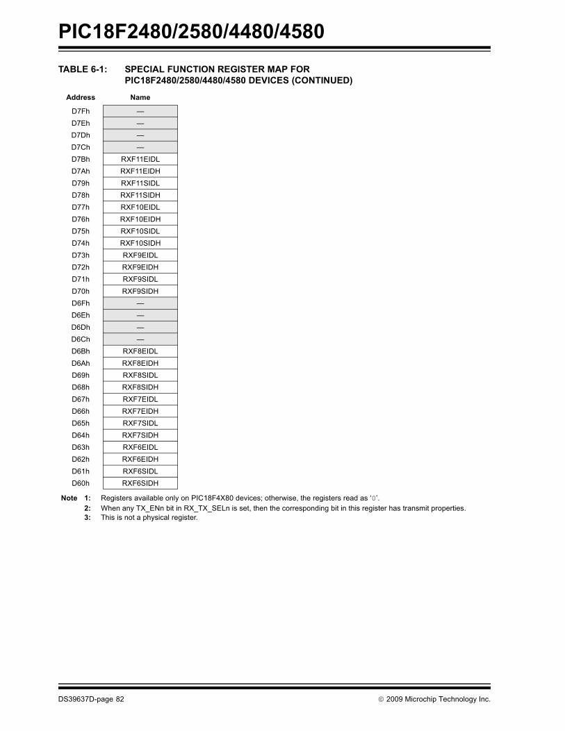
PIC18F2480/2580/4480/4580
Address Name
D7Fh —D7Eh —D7Dh —D7Ch —D7Bh RXF11EIDLD7Ah RXF11EIDHD79h RXF11SIDLD78h RXF11SIDHD77h RXF10EIDLD76h RXF10EIDHD75h RXF10SIDLD74h RXF10SIDHD73h RXF9EIDLD72h RXF9EIDHD71h RXF9SIDLD70h RXF9SIDHD6Fh —D6Eh —D6Dh —D6Ch —D6Bh RXF8EIDLD6Ah RXF8EIDHD69h RXF8SIDLD68h RXF8SIDHD67h RXF7EIDLD66h RXF7EIDHD65h RXF7SIDLD64h RXF7SIDHD63h RXF6EIDLD62h RXF6EIDHD61h RXF6SIDLD60h RXF6SIDH
TABLE 6-1: SPECIAL FUNCTION REGISTER MAP FOR PIC18F2480/2580/4480/4580 DEVICES (CONTINUED)
Note 1: Registers available only on PIC18F4X80 devices; otherwise, the registers read as ‘0’.2: When any TX_ENn bit in RX_TX_SELn is set, then the corresponding bit in this register has transmit properties.3: This is not a physical register.
DS39637D-page 82 © 2009 Microchip Technology Inc.

PIC18F2480/2580/4480/4580
TABLE 6-2: REGISTER FILE SUMMARY (PIC18F2480/2580/4480/4580)
File Name Bit 7 Bit 6 Bit 5 Bit 4 Bit 3 Bit 2 Bit 1 Bit 0 Value on POR, BOR
Details on Page:
TOSU — — — Top-of-Stack Upper Byte (TOS<20:16>) ---0 0000 55, 68
TOSH Top-of-Stack High Byte (TOS<15:8>) 0000 0000 55, 68
TOSL Top-of-Stack Low Byte (TOS<7:0>) 0000 0000 55, 68
STKPTR STKFUL STKUNF — Return Stack Pointer 00-0 0000 55, 69
PCLATU — — bit 21(1) Holding Register for PC<20:16> ---0 0000 55, 68
PCLATH Holding Register for PC<15:8> 0000 0000 55, 68
PCL PC Low Byte (PC<7:0>) 0000 0000 55, 68
TBLPTRU — — bit 21 Program Memory Table Pointer Upper Byte (TBLPTR<20:16>) --00 0000 55, 109
TBLPTRH Program Memory Table Pointer High Byte (TBLPTR<15:8>) 0000 0000 55, 109
TBLPTRL Program Memory Table Pointer Low Byte (TBLPTR<7:0>) 0000 0000 55, 109
TABLAT Program Memory Table Latch 0000 0000 55, 109
PRODH Product Register High Byte xxxx xxxx 55, 117
PRODL Product Register Low Byte xxxx xxxx 55, 117
INTCON GIE/GIEH PEIE/GIEL TMR0IE INT0IE RBIE TMR0IF INT0IF RBIF 0000 000x 55, 121
INTCON2 RBPU INTEDG0 INTEDG1 INTEDG2 — TMR0IP — RBIP 1111 -1-1 55, 122
INTCON3 INT2IP INT1IP — INT2IE INT1IE — INT2IF INT1IF 11-0 0-00 55, 123
INDF0 Uses contents of FSR0 to address data memory – value of FSR0 not changed (not a physical register) N/A 55, 96
POSTINC0 Uses contents of FSR0 to address data memory – value of FSR0 post-incremented (not a physical register) N/A 55, 97
POSTDEC0 Uses contents of FSR0 to address data memory – value of FSR0 post-decremented (not a physical register) N/A 55, 97
PREINC0 Uses contents of FSR0 to address data memory – value of FSR0 pre-incremented (not a physical register) N/A 55, 97
PLUSW0 Uses contents of FSR0 to address data memory – value of FSR0 pre-incremented (not a physical register), value of FSR0 offset by W
N/A 55, 97
FSR0H — — — — Indirect Data Memory Address Pointer 0 High ---- xxxx 55, 96
FSR0L Indirect Data Memory Address Pointer 0 Low Byte xxxx xxxx 55, 96
WREG Working Register xxxx xxxx 55
INDF1 Uses contents of FSR1 to address data memory – value of FSR1 not changed (not a physical register) N/A 55, 96
POSTINC1 Uses contents of FSR1 to address data memory – value of FSR1 post-incremented (not a physical register) N/A 55, 97
POSTDEC1 Uses contents of FSR1 to address data memory – value of FSR1 post-decremented (not a physical register) N/A 55, 97
PREINC1 Uses contents of FSR1 to address data memory – value of FSR1 pre-incremented (not a physical register) N/A 55, 97
PLUSW1 Uses contents of FSR1 to address data memory – value of FSR1 pre-incremented (not a physical register), value of FSR1 offset by W
N/A 55, 97
FSR1H — — — — Indirect Data Memory Address Pointer 1 High ---- xxxx 55, 96
FSR1L Indirect Data Memory Address Pointer 1 Low Byte xxxx xxxx 55, 96
BSR — — — — Bank Select Register ---- 0000 56, 73
INDF2 Uses contents of FSR2 to address data memory – value of FSR2 not changed (not a physical register) N/A 56, 96
POSTINC2 Uses contents of FSR2 to address data memory – value of FSR2 post-incremented (not a physical register) N/A 56, 97
POSTDEC2 Uses contents of FSR2 to address data memory – value of FSR2 post-decremented (not a physical register) N/A 56, 97
PREINC2 Uses contents of FSR2 to address data memory – value of FSR2 pre-incremented (not a physical register) N/A 56, 97
PLUSW2 Uses contents of FSR2 to address data memory – value of FSR2 pre-incremented (not a physical register), value of FSR2 offset by W
N/A 56, 97
Legend: x = unknown, u = unchanged, - = unimplemented, q = value depends on conditionNote 1: Bit 21 of the PC is only available in Test mode and Serial Programming modes.
2: The SBOREN bit is only available when CONFIG2L<1:0> = 01; otherwise, it is disabled and reads as ‘0’. See Section 5.4 “Brown-out Reset (BOR)”.3: These registers and/or bits are not implemented on PIC18F2X80 devices and are read as ‘0’. Reset values are shown for PIC18F4X80 devices;
individual unimplemented bits should be interpreted as ‘—’.4: The PLLEN bit is only available in specific oscillator configuration; otherwise, it is disabled and reads as ‘0’. See Section 3.6.4 “PLL in INTOSC
Modes”.5: The RE3 bit is only available when Master Clear Reset is disabled (CONFIG3H<7> = 0); otherwise, RE3 reads as ‘0’. This bit is read-only.6: RA6/RA7 and their associated latch and direction bits are individually configured as port pins based on various primary oscillator modes. When
disabled, these bits read as ‘0’.7: CAN bits have multiple functions depending on the selected mode of the CAN module.8: This register reads all ‘0’s until the ECAN™ technology is set up in Mode 1 or Mode 2.9: These registers are available on PIC18F4X80 devices only.
© 2009 Microchip Technology Inc. DS39637D-page 83

PIC18F2480/2580/4480/4580
FSR2H — — — — Indirect Data Memory Address Pointer 2 High ---- xxxx 56, 96
FSR2L Indirect Data Memory Address Pointer 2 Low Byte xxxx xxxx 56, 96
STATUS — — — N OV Z DC C ---x xxxx 56, 94
TMR0H Timer0 Register High Byte 0000 0000 56, 153
TMR0L Timer0 Register Low Byte xxxx xxxx 56, 153
T0CON TMR0ON T08BIT T0CS T0SE PSA T0PS2 T0PS1 T0PS0 1111 1111 56, 153
OSCCON IDLEN IRCF2 IRCF1 IRCF0 OSTS IOFS SCS1 SCS0 0000 q000 36, 56
HLVDCON VDIRMAG — IRVST HLVDEN HLVDL3 HLVDL2 HLVDL1 HLVDL0 0-00 0101 56, 273
WDTCON — — — — — — — SWDTEN --- ---0 56, 359
RCON IPEN SBOREN(2) — RI TO PD POR BOR 0q-1 11q0 56, 133
TMR1H Timer1 Register High Byte xxxx xxxx 56, 159
TMR1L Timer1 Register Low Byte 0000 0000 56, 159
T1CON RD16 T1RUN T1CKPS1 T1CKPS0 T1OSCEN T1SYNC TMR1CS TMR1ON 0000 0000 56, 155
TMR2 Timer2 Register 1111 1111 56, 162
PR2 Timer2 Period Register -000 0000 56, 159
T2CON — T2OUTPS3 T2OUTPS2 T2OUTPS1 T2OUTPS0 TMR2ON T2CKPS1 T2CKPS0 -000 0000 56, 161
SSPBUF MSSP Receive Buffer/Transmit Register xxxx xxxx 56, 199
SSPADD MSSP Address Register in I2C Slave Mode. MSSP Baud Rate Reload Register in I2C Master Mode. 0000 0000 56, 199
SSPSTAT SMP CKE D/A P S R/W UA BF 0000 0000 56, 201
SSPCON1 WCOL SSPOV SSPEN CKP SSPM3 SSPM2 SSPM1 SSPM0 0000 0000 56, 202
SSPCON2 GCEN ACKSTAT ACKDT ACKEN RCEN PEN RSEN SEN 0000 0000 56, 203
ADRESH A/D Result Register High Byte xxxx xxxx 56, 262
ADRESL A/D Result Register Low Byte xxxx xxxx 56, 262
ADCON0 — — CHS3 CHS2 CHS1 CHS0 GO/DONE ADON --00 0000 56, 253
ADCON1 — — VCFG1 VCFG0 PCFG3 PCFG2 PCFG1 PCFG0 --00 0qqq 56, 254
ADCON2 ADFM — ACQT2 ACQT1 ACQT0 ADCS2 ADCS1 ADCS0 0-00 0000 57, 255
CCPR1H Capture/Compare/PWM Register 1 High Byte xxxx xxxx 57, 172
CCPR1L Capture/Compare/PWM Register 1 Low Byte xxxx xxxx 57, 172
CCP1CON — — DC1B1 DC1B0 CCP1M3 CCP1M2 CCP1M1 CCP1M0 --00 0000 57, 167
ECCPR1H(9) Enhanced Capture/Compare/PWM Register 1 High Byte xxxx xxxx 57, 171
ECCPR1L(9) Enhanced Capture/Compare/PWM Register 1 Low Byte xxxx xxxx 57, 171
ECCP1CON(9) EPWM1M1 EPWM1M0 EDC1B1 EDC1B0 ECCP1M3 ECCP1M2 ECCP1M1 ECCP1M0 0000 0000 57, 172
BAUDCON ABDOVF RCIDL — SCKP BRG16 — WUE ABDEN 01-0 0000 57, 234
ECCP1DEL(9) PRSEN PDC6(3) PDC5(3) PDC4(3) PDC3(3) PDC2(3) PDC1(3) PDC0(3) 0000 0000 57, 187
ECCP1AS(9) ECCPASE ECCPAS2 ECCPAS1 ECCPAS0 PSSAC1 PSSAC0 PSSBD1(3) PSSBD0(3) 0000 0000 57, 187
CVRCON(9) CVREN CVROE CVRR CVRSS CVR3 CVR2 CVR1 CVR0 0000 0000 57, 269
CMCON(9) C2OUT C1OUT C2INV C1INV CIS CM2 CM1 CM0 0000 0000 57, 263
TMR3H Timer3 Register High Byte xxxx xxxx 57, 165
TMR3L Timer3 Register Low Byte xxxx xxxx 57, 165
T3CON RD16 T3ECCP1(9) T3CKPS1 T3CKPS0 T3CCP1(9) T3SYNC TMR3CS TMR3ON 0000 0000 57, 165
TABLE 6-2: REGISTER FILE SUMMARY (PIC18F2480/2580/4480/4580) (CONTINUED)
File Name Bit 7 Bit 6 Bit 5 Bit 4 Bit 3 Bit 2 Bit 1 Bit 0 Value on POR, BOR
Details on Page:
Legend: x = unknown, u = unchanged, - = unimplemented, q = value depends on conditionNote 1: Bit 21 of the PC is only available in Test mode and Serial Programming modes.
2: The SBOREN bit is only available when CONFIG2L<1:0> = 01; otherwise, it is disabled and reads as ‘0’. See Section 5.4 “Brown-out Reset (BOR)”.3: These registers and/or bits are not implemented on PIC18F2X80 devices and are read as ‘0’. Reset values are shown for PIC18F4X80 devices;
individual unimplemented bits should be interpreted as ‘—’.4: The PLLEN bit is only available in specific oscillator configuration; otherwise, it is disabled and reads as ‘0’. See Section 3.6.4 “PLL in INTOSC
Modes”.5: The RE3 bit is only available when Master Clear Reset is disabled (CONFIG3H<7> = 0); otherwise, RE3 reads as ‘0’. This bit is read-only.6: RA6/RA7 and their associated latch and direction bits are individually configured as port pins based on various primary oscillator modes. When
disabled, these bits read as ‘0’.7: CAN bits have multiple functions depending on the selected mode of the CAN module.8: This register reads all ‘0’s until the ECAN™ technology is set up in Mode 1 or Mode 2.9: These registers are available on PIC18F4X80 devices only.
DS39637D-page 84 © 2009 Microchip Technology Inc.

PIC18F2480/2580/4480/4580
SPBRGH EUSART Baud Rate Generator High Byte 0000 0000 57, 236
SPBRG EUSART Baud Rate Generator 0000 0000 57, 236
RCREG EUSART Receive Register 0000 0000 57, 244
TXREG EUSART Transmit Register 0000 0000 57, 241
TXSTA CSRC TX9 TXEN SYNC SENDB BRGH TRMT TX9D 0000 0010 57, 243
RCSTA SPEN RX9 SREN CREN ADDEN FERR OERR RX9D 0000 000x 57, 243
EEADR EEPROM Address Register 0000 0000 57, 111
EEDATA EEPROM Data Register 0000 0000 57, 111
EECON2 EEPROM Control Register 2 (not a physical register) 0000 0000 57, 111
EECON1 EEPGD CFGS — FREE WRERR WREN WR RD xx-0 x000 57, 111
IPR3Mode 0
IRXIP WAKIP ERRIP TXB2IP TXB1IP TXB0IP RXB1IP RXB0IP 1111 1111 57, 132
IPR3Mode 1, 2
IRXIP WAKIP ERRIP TXBnIP TXB1IP(8) TXB0IP(8) RXBnIP FIFOWMIP 1111 1111 57, 132
PIR3Mode 0
IRXIF WAKIF ERRIF TXB2IF TXB1IF TXB0IF RXB1IF RXB0IF 0000 0000 57, 126
PIR3Mode 1, 2
IRXIF WAKIF ERRIF TXBnIF TXB1IF(8) TXB0IF(8) RXBnIF FIFOWMIF 0000 0000 57, 126
PIE3Mode 0
IRXIE WAKIE ERRIE TXB2IE TXB1IE TXB0IE RXB1IE RXB0IE 0000 0000 57, 129
PIE3Mode 1, 2
IRXIE WAKIE ERRIE TXBnIE TXB1IE(8) TXB0IE(8) RXBnIE FIFOMWIE 0000 0000 57, 129
IPR2 OSCFIP CMIP(9) — EEIP BCLIP HLVDIP TMR3IP ECCP1IP(9) 11-1 1111 57, 131
PIR2 OSCFIF CMIF(9) — EEIF BCLIF HLVDIF TMR3IF ECCP1IF(9) 00-0 0000 58, 125
PIE2 OSCFIE CMIE(9) — EEIE BCLIE HLVDIE TMR3IE ECCP1IE(9) 00-0 0000 58, 128
IPR1 PSPIP(3) ADIP RCIP TXIP SSPIP CCP1IP TMR2IP TMR1IP 1111 1111 58, 130
PIR1 PSPIF(3) ADIF RCIF TXIF SSPIF CCP1IF TMR2IF TMR1IF 0000 0000 58, 124
PIE1 PSPIE(3) ADIE RCIE TXIE SSPIE CCP1IE TMR2IE TMR1IE 0000 0000 58, 127
OSCTUNE INTSRC PLLEN(4) — TUN4 TUN3 TUN2 TUN1 TUN0 0q-0 0000 33, 58
TRISE(3) IBF OBF IBOV PSPMODE — TRISE2 TRISE1 TRISE0 0000 -111 58, 146
TRISD(3) PORTD Data Direction Register 1111 1111 58, 143
TRISC PORTC Data Direction Register 1111 1111 58, 141
TRISB PORTB Data Direction Register 1111 1111 58, 138
TRISA TRISA7(6) TRISA6(6) PORTA Data Direction Register 1111 1111 58, 135
LATE(3) — — — — — LATE2 LATE1 LATE0 ---- -xxx 58, 146
LATD(3) LATD Output Latch Register xxxx xxxx 58, 143
LATC LATC Output Latch Register xxxx xxxx 58, 141
LATB LATB Output Latch Register xxxx xxxx 58, 138
LATA LATA7(6) LATA6(6) LATA Output Latch Register xxxx xxxx 58, 135
TABLE 6-2: REGISTER FILE SUMMARY (PIC18F2480/2580/4480/4580) (CONTINUED)
File Name Bit 7 Bit 6 Bit 5 Bit 4 Bit 3 Bit 2 Bit 1 Bit 0 Value on POR, BOR
Details on Page:
Legend: x = unknown, u = unchanged, - = unimplemented, q = value depends on conditionNote 1: Bit 21 of the PC is only available in Test mode and Serial Programming modes.
2: The SBOREN bit is only available when CONFIG2L<1:0> = 01; otherwise, it is disabled and reads as ‘0’. See Section 5.4 “Brown-out Reset (BOR)”.3: These registers and/or bits are not implemented on PIC18F2X80 devices and are read as ‘0’. Reset values are shown for PIC18F4X80 devices;
individual unimplemented bits should be interpreted as ‘—’.4: The PLLEN bit is only available in specific oscillator configuration; otherwise, it is disabled and reads as ‘0’. See Section 3.6.4 “PLL in INTOSC
Modes”.5: The RE3 bit is only available when Master Clear Reset is disabled (CONFIG3H<7> = 0); otherwise, RE3 reads as ‘0’. This bit is read-only.6: RA6/RA7 and their associated latch and direction bits are individually configured as port pins based on various primary oscillator modes. When
disabled, these bits read as ‘0’.7: CAN bits have multiple functions depending on the selected mode of the CAN module.8: This register reads all ‘0’s until the ECAN™ technology is set up in Mode 1 or Mode 2.9: These registers are available on PIC18F4X80 devices only.
© 2009 Microchip Technology Inc. DS39637D-page 85

PIC18F2480/2580/4480/4580
PORTE(3) — — — — RE3(5) RE2(3) RE1(3) RE0(3) ---- xxxx 58, 150
PORTD(3) PORTD Data Direction Register xxxx xxxx 58, 143
PORTC PORTC Data Direction Register xxxx xxxx 58, 141
PORTB PORTB Data Direction Register xxxx xxxx 58, 138
PORTA RA7(6) RA6(6) PORTA Data Direction Register xx00 0000 58, 135
ECANCON MDSEL1 MDSEL0 FIFOWM EWIN4 EWIN3 EWIN2 EWIN1 EWIN0 0001 000 58, 286
TXERRCNT TEC7 TEC6 TEC5 TEC4 TEC3 TEC2 TEC1 TEC0 0000 0000 58, 291
RXERRCNT REC7 REC6 REC5 REC4 REC3 REC2 REC1 REC0 0000 0000 58, 299
COMSTATMode 0
RXB0OVFL RXB1OVFL TXBO TXBP RXBP TXWARN RXWARN EWARN 0000 0000 58, 287
COMSTATMode 1
— RXBnOVFL TXBO TXBP RXBP TXWARN RXWARN EWARN -000 0000 58, 287
COMSTATMode 2
FIFOEMPTY RXBnOVFL TXBO TXBP RXBP TXWARN RXWARN EWARN 0000 0000 58, 287
CIOCON — — ENDRHI CANCAP — — — — --00 ---- 58, 320
BRGCON3 WAKDIS WAKFIL — — — SEG2PH2 SEG2PH1 SEG2PH0 00-- -000 59, 319
BRGCON2 SEG2PHTS SAM SEG1PH2 SEG1PH1 SEG1PH0 PRSEG2 PRSEG1 PRSEG0 0000 0000 59, 318
BRGCON1 SJW1 SJW0 BRP5 BRP4 BRP3 BRP2 BRP1 BRP0 0000 0000 59, 317
CANCONMode 0
REQOP2 REQOP1 REQOP0 ABAT WIN2(7) WIN1(7) WIN0(7) —(7) 1000 000- 59, 282
CANCONMode 1
REQOP2 REQOP1 REQOP0 ABAT —(7) —(7) —(7) —(7) 1000 ---- 59, 282
CANCONMode 2
REQOP2 REQOP1 REQOP0 ABAT FP3(7) FP2(7) FP1(7) FP0(7) 1000 0000 59, 282
CANSTATMode 0
OPMODE2 OPMODE1 OPMODE0 —(7) ICODE3(7) ICODE2(7) ICODE1(7) —(7) 000- 0000 59, 283
CANSTATModes 1, 2
OPMODE2 OPMODE1 OPMODE0 EICODE4(7) EICODE3(7) EICODE2(7) EICODE1(7) EICODE0(7) 0000 0000 59, 283
RXB0D7 RXB0D77 RXB0D76 RXB0D75 RXB0D74 RXB0D73 RXB0D72 RXB0D71 RXB0D70 xxxx xxxx 59, 298
RXB0D6 RXB0D67 RXB0D66 RXB0D65 RXB0D64 RXB0D63 RXB0D62 RXB0D61 RXB0D60 xxxx xxxx 59, 298
RXB0D5 RXB0D57 RXB0D56 RXB0D55 RXB0D54 RXB0D53 RXB0D52 RXB0D51 RXB0D50 xxxx xxxx 59, 298
RXB0D4 RXB0D47 RXB0D46 RXB0D45 RXB0D44 RXB0D43 RXB0D42 RXB0D41 RXB0D40 xxxx xxxx 59, 298
RXB0D3 RXB0D37 RXB0D36 RXB0D35 RXB0D34 RXB0D33 RXB0D32 RXB0D31 RXB0D30 xxxx xxxx 59, 298
RXB0D2 RXB0D27 RXB0D26 RXB0D25 RXB0D24 RXB0D23 RXB0D22 RXB0D21 RXB0D20 xxxx xxxx 59, 298
RXB0D1 RXB0D17 RXB0D16 RXB0D15 RXB0D14 RXB0D13 RXB0D12 RXB0D11 RXB0D10 xxxx xxxx 59, 298
RXB0D0 RXB0D07 RXB0D06 RXB0D05 RXB0D04 RXB0D03 RXB0D02 RXB0D01 RXB0D00 xxxx xxxx 59, 298
RXB0DLC — RXRTR RB1 RB0 DLC3 DLC2 DLC1 DLC0 -xxx xxxx 59, 298
RXB0EIDL EID7 EID6 EID5 EID4 EID3 EID2 EID1 EID0 xxxx xxxx 59, 297
RXB0EIDH EID15 EID14 EID13 EID12 EID11 EID10 EID9 EID8 xxxx xxxx 59, 297
RXB0SIDL SID2 SID1 SID0 SRR EXID — EID17 EID16 xxxx x-xx 59, 297
RXB0SIDH SID10 SID9 SID8 SID7 SID6 SID5 SID4 SID3 xxxx xxxx 59, 296
TABLE 6-2: REGISTER FILE SUMMARY (PIC18F2480/2580/4480/4580) (CONTINUED)
File Name Bit 7 Bit 6 Bit 5 Bit 4 Bit 3 Bit 2 Bit 1 Bit 0 Value on POR, BOR
Details on Page:
Legend: x = unknown, u = unchanged, - = unimplemented, q = value depends on conditionNote 1: Bit 21 of the PC is only available in Test mode and Serial Programming modes.
2: The SBOREN bit is only available when CONFIG2L<1:0> = 01; otherwise, it is disabled and reads as ‘0’. See Section 5.4 “Brown-out Reset (BOR)”.3: These registers and/or bits are not implemented on PIC18F2X80 devices and are read as ‘0’. Reset values are shown for PIC18F4X80 devices;
individual unimplemented bits should be interpreted as ‘—’.4: The PLLEN bit is only available in specific oscillator configuration; otherwise, it is disabled and reads as ‘0’. See Section 3.6.4 “PLL in INTOSC
Modes”.5: The RE3 bit is only available when Master Clear Reset is disabled (CONFIG3H<7> = 0); otherwise, RE3 reads as ‘0’. This bit is read-only.6: RA6/RA7 and their associated latch and direction bits are individually configured as port pins based on various primary oscillator modes. When
disabled, these bits read as ‘0’.7: CAN bits have multiple functions depending on the selected mode of the CAN module.8: This register reads all ‘0’s until the ECAN™ technology is set up in Mode 1 or Mode 2.9: These registers are available on PIC18F4X80 devices only.
DS39637D-page 86 © 2009 Microchip Technology Inc.
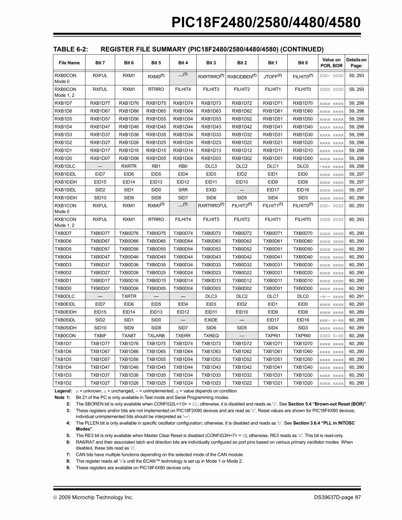
PIC18F2480/2580/4480/4580
RXB0CONMode 0
RXFUL RXM1 RXM0(7) —(7)RXRTRRO(7) RXBODBEN(7) JTOFF(7) FILHIT0(7) 000- 0000 59, 293
RXB0CONMode 1, 2
RXFUL RXM1 RTRRO FILHIT4 FILHIT3 FILHIT2 FILHIT1 FILHIT0 0000 0000 59, 293
RXB1D7 RXB1D77 RXB1D76 RXB1D75 RXB1D74 RXB1D73 RXB1D72 RXB1D71 RXB1D70 xxxx xxxx 59, 298
RXB1D6 RXB1D67 RXB1D66 RXB1D65 RXB1D64 RXB1D63 RXB1D62 RXB1D61 RXB1D60 xxxx xxxx 59, 298
RXB1D5 RXB1D57 RXB1D56 RXB1D55 RXB1D54 RXB1D53 RXB1D52 RXB1D51 RXB1D50 xxxx xxxx 59, 298
RXB1D4 RXB1D47 RXB1D46 RXB1D45 RXB1D44 RXB1D43 RXB1D42 RXB1D41 RXB1D40 xxxx xxxx 59, 298
RXB1D3 RXB1D37 RXB1D36 RXB1D35 RXB1D34 RXB1D33 RXB1D32 RXB1D31 RXB1D30 xxxx xxxx 59, 298
RXB1D2 RXB1D27 RXB1D26 RXB1D25 RXB1D24 RXB1D23 RXB1D22 RXB1D21 RXB1D20 xxxx xxxx 59, 298
RXB1D1 RXB1D17 RXB1D16 RXB1D15 RXB1D14 RXB1D13 RXB1D12 RXB1D11 RXB1D10 xxxx xxxx 59, 298
RXB1D0 RXB1D07 RXB1D06 RXB1D05 RXB1D04 RXB1D03 RXB1D02 RXB1D01 RXB1D00 xxxx xxxx 59, 298
RXB1DLC — RXRTR RB1 RB0 DLC3 DLC2 DLC1 DLC0 -xxx xxxx 59, 298
RXB1EIDL EID7 EID6 EID5 EID4 EID3 EID2 EID1 EID0 xxxx xxxx 59, 297
RXB1EIDH EID15 EID14 EID13 EID12 EID11 EID10 EID9 EID8 xxxx xxxx 59, 297
RXB1SIDL SID2 SID1 SID0 SRR EXID — EID17 EID16 xxxx xxxx 59, 297
RXB1SIDH SID10 SID9 SID8 SID7 SID6 SID5 SID4 SID3 xxxx xxxx 60, 296
RXB1CONMode 0
RXFUL RXM1 RXM0(7) —(7) RXRTRRO(7) FILHIT2(7) FILHIT1(7) FILHIT0(7) 000- 0000 60, 293
RXB1CONMode 1, 2
RXFUL RXM1 RTRRO FILHIT4 FILHIT3 FILHIT2 FILHIT1 FILHIT0 0000 0000 60, 293
TXB0D7 TXB0D77 TXB0D76 TXB0D75 TXB0D74 TXB0D73 TXB0D72 TXB0D71 TXB0D70 xxxx xxxx 60, 290
TXB0D6 TXB0D67 TXB0D66 TXB0D65 TXB0D64 TXB0D63 TXB0D62 TXB0D61 TXB0D60 xxxx xxxx 60, 290
TXB0D5 TXB0D57 TXB0D56 TXB0D55 TXB0D54 TXB0D53 TXB0D52 TXB0D51 TXB0D50 xxxx xxxx 60, 290
TXB0D4 TXB0D47 TXB0D46 TXB0D45 TXB0D44 TXB0D43 TXB0D42 TXB0D41 TXB0D40 xxxx xxxx 60, 290
TXB0D3 TXB0D37 TXB0D36 TXB0D35 TXB0D34 TXB0D33 TXB0D32 TXB0D31 TXB0D30 xxxx xxxx 60, 290
TXB0D2 TXB0D27 TXB0D26 TXB0D25 TXB0D24 TXB0D23 TXB0D22 TXB0D21 TXB0D20 xxxx xxxx 60, 290
TXB0D1 TXB0D17 TXB0D16 TXB0D15 TXB0D14 TXB0D13 TXB0D12 TXB0D11 TXB0D10 xxxx xxxx 60, 290
TXB0D0 TXB0D07 TXB0D06 TXB0D05 TXB0D04 TXB0D03 TXB0D02 TXB0D01 TXB0D00 xxxx xxxx 60, 290
TXB0DLC — TXRTR — — DLC3 DLC2 DLC1 DLC0 -x-- xxxx 60, 291
TXB0EIDL EID7 EID6 EID5 EID4 EID3 EID2 EID1 EID0 xxxx xxxx 60, 290
TXB0EIDH EID15 EID14 EID13 EID12 EID11 EID10 EID9 EID8 xxxx xxxx 60, 289
TXB0SIDL SID2 SID1 SID0 — EXIDE — EID17 EID16 xxx- x-xx 60, 289
TXB0SIDH SID10 SID9 SID8 SID7 SID6 SID5 SID4 SID3 xxxx xxxx 60, 289
TXB0CON TXBIF TXABT TXLARB TXERR TXREQ — TXPRI1 TXPRI0 0000 0-00 60, 288
TXB1D7 TXB1D77 TXB1D76 TXB1D75 TXB1D74 TXB1D73 TXB1D72 TXB1D71 TXB1D70 xxxx xxxx 60, 290
TXB1D6 TXB1D67 TXB1D66 TXB1D65 TXB1D64 TXB1D63 TXB1D62 TXB1D61 TXB1D60 xxxx xxxx 60, 290
TXB1D5 TXB1D57 TXB1D56 TXB1D55 TXB1D54 TXB1D53 TXB1D52 TXB1D51 TXB1D50 xxxx xxxx 60, 290
TXB1D4 TXB1D47 TXB1D46 TXB1D45 TXB1D44 TXB1D43 TXB1D42 TXB1D41 TXB1D40 xxxx xxxx 60, 290
TXB1D3 TXB1D37 TXB1D36 TXB1D35 TXB1D34 TXB1D33 TXB1D32 TXB1D31 TXB1D30 xxxx xxxx 60, 290
TXB1D2 TXB1D27 TXB1D26 TXB1D25 TXB1D24 TXB1D23 TXB1D22 TXB1D21 TXB1D20 xxxx xxxx 60, 290
TABLE 6-2: REGISTER FILE SUMMARY (PIC18F2480/2580/4480/4580) (CONTINUED)
File Name Bit 7 Bit 6 Bit 5 Bit 4 Bit 3 Bit 2 Bit 1 Bit 0 Value on POR, BOR
Details on Page:
Legend: x = unknown, u = unchanged, - = unimplemented, q = value depends on conditionNote 1: Bit 21 of the PC is only available in Test mode and Serial Programming modes.
2: The SBOREN bit is only available when CONFIG2L<1:0> = 01; otherwise, it is disabled and reads as ‘0’. See Section 5.4 “Brown-out Reset (BOR)”.3: These registers and/or bits are not implemented on PIC18F2X80 devices and are read as ‘0’. Reset values are shown for PIC18F4X80 devices;
individual unimplemented bits should be interpreted as ‘—’.4: The PLLEN bit is only available in specific oscillator configuration; otherwise, it is disabled and reads as ‘0’. See Section 3.6.4 “PLL in INTOSC
Modes”.5: The RE3 bit is only available when Master Clear Reset is disabled (CONFIG3H<7> = 0); otherwise, RE3 reads as ‘0’. This bit is read-only.6: RA6/RA7 and their associated latch and direction bits are individually configured as port pins based on various primary oscillator modes. When
disabled, these bits read as ‘0’.7: CAN bits have multiple functions depending on the selected mode of the CAN module.8: This register reads all ‘0’s until the ECAN™ technology is set up in Mode 1 or Mode 2.9: These registers are available on PIC18F4X80 devices only.
© 2009 Microchip Technology Inc. DS39637D-page 87

PIC18F2480/2580/4480/4580
TXB1D1 TXB1D17 TXB1D16 TXB1D15 TXB1D14 TXB1D13 TXB1D12 TXB1D11 TXB1D10 xxxx xxxx 60, 290
TXB1D0 TXB1D07 TXB1D06 TXB1D05 TXB1D04 TXB1D03 TXB1D02 TXB1D01 TXB1D00 xxxx xxxx 60, 290
TXB1DLC — TXRTR — — DLC3 DLC2 DLC1 DLC0 -x-- xxxx 60, 291
TXB1EIDL EID7 EID6 EID5 EID4 EID3 EID2 EID1 EID0 xxxx xxxx 60, 290
TXB1EIDH EID15 EID14 EID13 EID12 EID11 EID10 EID9 EID8 xxxx xxxx 60, 289
TXB1SIDL SID2 SID1 SID0 — EXIDE — EID17 EID16 xxx- x-xx 60, 289
TXB1SIDH SID10 SID9 SID8 SID7 SID6 SID5 SID4 SID3 xxxx xxxx 60, 289
TXB1CON TXBIF TXABT TXLARB TXERR TXREQ — TXPRI1 TXPRI0 0000 0-00 60, 288
TXB2D7 TXB2D77 TXB2D76 TXB2D75 TXB2D74 TXB2D73 TXB2D72 TXB2D71 TXB2D70 xxxx xxxx 60, 290
TXB2D6 TXB2D67 TXB2D66 TXB2D65 TXB2D64 TXB2D63 TXB2D62 TXB2D61 TXB2D60 xxxx xxxx 61, 290
TXB2D5 TXB2D57 TXB2D56 TXB2D55 TXB2D54 TXB2D53 TXB2D52 TXB2D51 TXB2D50 xxxx xxxx 61, 290
TXB2D4 TXB2D47 TXB2D46 TXB2D45 TXB2D44 TXB2D43 TXB2D42 TXB2D41 TXB2D40 xxxx xxxx 61, 290
TXB2D3 TXB2D37 TXB2D36 TXB2D35 TXB2D34 TXB2D33 TXB2D32 TXB2D31 TXB2D30 xxxx xxxx 61, 290
TXB2D2 TXB2D27 TXB2D26 TXB2D25 TXB2D24 TXB2D23 TXB2D22 TXB2D21 TXB2D20 xxxx xxxx 61, 290
TXB2D1 TXB2D17 TXB2D16 TXB2D15 TXB2D14 TXB2D13 TXB2D12 TXB2D11 TXB2D10 xxxx xxxx 61, 290
TXB2D0 TXB2D07 TXB2D06 TXB2D05 TXB2D04 TXB2D03 TXB2D02 TXB2D01 TXB2D00 xxxx xxxx 61, 290
TXB2DLC — TXRTR — — DLC3 DLC2 DLC1 DLC0 -x-- xxxx 61, 291
TXB2EIDL EID7 EID6 EID5 EID4 EID3 EID2 EID1 EID0 xxxx xxxx 61, 290
TXB2EIDH EID15 EID14 EID13 EID12 EID11 EID10 EID9 EID8 xxxx xxxx 61, 289
TXB2SIDL SID2 SID1 SID0 — EXIDE — EID17 EID16 xxxx x-xx 61, 289
TXB2SIDH SID10 SID9 SID8 SID7 SID6 SID5 SID4 SID3 xxx- x-xx 61, 289
TXB2CON TXBIF TXABT TXLARB TXERR TXREQ — TXPRI1 TXPRI0 0000 0-00 61, 288
RXM1EIDL EID7 EID6 EID5 EID4 EID3 EID2 EID1 EID0 xxxx xxxx 61, 310
RXM1EIDH EID15 EID14 EID13 EID12 EID11 EID10 EID9 EID8 xxxx xxxx 61, 310
RXM1SIDL SID2 SID1 SID0 — EXIDEN — EID17 EID16 xxx- x-xx 61, 310
RXM1SIDH SID10 SID9 SID8 SID7 SID6 SID5 SID4 SID3 xxxx xxxx 61, 310
RXM0EIDL EID7 EID6 EID5 EID4 EID3 EID2 EID1 EID0 xxxx xxxx 61, 310
RXM0EIDH EID15 EID14 EID13 EID12 EID11 EID10 EID9 EID8 xxxx xxxx 61, 310
RXM0SIDL SID2 SID1 SID0 — EXIDEN — EID17 EID16 xxx- x-xx 61, 310
RXM0SIDH SID10 SID9 SID8 SID7 SID6 SID5 SID4 SID3 xxxx xxxx 61, 309
RXF5EIDL EID7 EID6 EID5 EID4 EID3 EID2 EID1 EID0 xxxx xxxx 61, 309
RXF5EIDH EID15 EID14 EID13 EID12 EID11 EID10 EID9 EID8 xxxx xxxx 61, 309
RXF5SIDL SID2 SID1 SID0 — EXIDEN — EID17 EID16 xxx- x-xx 61, 308
RXF5SIDH SID10 SID9 SID8 SID7 SID6 SID5 SID4 SID3 xxxx xxxx 61, 308
RXF4EIDL EID7 EID6 EID5 EID4 EID3 EID2 EID1 EID0 xxxx xxxx 61, 309
RXF4EIDH EID15 EID14 EID13 EID12 EID11 EID10 EID9 EID8 xxxx xxxx 61, 309
RXF4SIDL SID2 SID1 SID0 — EXIDEN — EID17 EID16 xxx- x-xx 61, 308
RXF4SIDH SID10 SID9 SID8 SID7 SID6 SID5 SID4 SID3 xxxx xxxx 61, 308
RXF3EIDL EID7 EID6 EID5 EID4 EID3 EID2 EID1 EID0 xxxx xxxx 61, 309
RXF3EIDH EID15 EID14 EID13 EID12 EID11 EID10 EID9 EID8 xxxx xxxx 61, 309
RXF3SIDL SID2 SID1 SID0 — EXIDEN — EID17 EID16 xxx- x-xx 62, 308
TABLE 6-2: REGISTER FILE SUMMARY (PIC18F2480/2580/4480/4580) (CONTINUED)
File Name Bit 7 Bit 6 Bit 5 Bit 4 Bit 3 Bit 2 Bit 1 Bit 0 Value on POR, BOR
Details on Page:
Legend: x = unknown, u = unchanged, - = unimplemented, q = value depends on conditionNote 1: Bit 21 of the PC is only available in Test mode and Serial Programming modes.
2: The SBOREN bit is only available when CONFIG2L<1:0> = 01; otherwise, it is disabled and reads as ‘0’. See Section 5.4 “Brown-out Reset (BOR)”.3: These registers and/or bits are not implemented on PIC18F2X80 devices and are read as ‘0’. Reset values are shown for PIC18F4X80 devices;
individual unimplemented bits should be interpreted as ‘—’.4: The PLLEN bit is only available in specific oscillator configuration; otherwise, it is disabled and reads as ‘0’. See Section 3.6.4 “PLL in INTOSC
Modes”.5: The RE3 bit is only available when Master Clear Reset is disabled (CONFIG3H<7> = 0); otherwise, RE3 reads as ‘0’. This bit is read-only.6: RA6/RA7 and their associated latch and direction bits are individually configured as port pins based on various primary oscillator modes. When
disabled, these bits read as ‘0’.7: CAN bits have multiple functions depending on the selected mode of the CAN module.8: This register reads all ‘0’s until the ECAN™ technology is set up in Mode 1 or Mode 2.9: These registers are available on PIC18F4X80 devices only.
DS39637D-page 88 © 2009 Microchip Technology Inc.
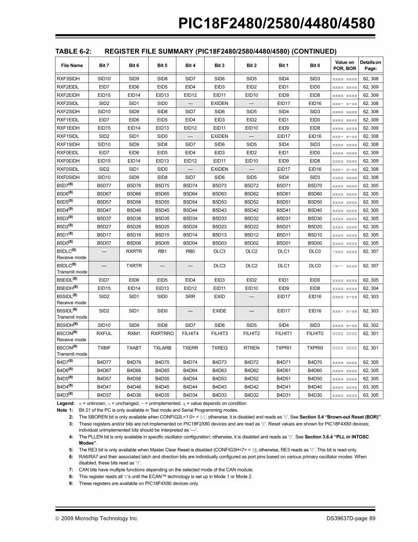
PIC18F2480/2580/4480/4580
RXF3SIDH SID10 SID9 SID8 SID7 SID6 SID5 SID4 SID3 xxxx xxxx 62, 308
RXF2EIDL EID7 EID6 EID5 EID4 EID3 EID2 EID1 EID0 xxxx xxxx 62, 309
RXF2EIDH EID15 EID14 EID13 EID12 EID11 EID10 EID9 EID8 xxxx xxxx 62, 309
RXF2SIDL SID2 SID1 SID0 — EXIDEN — EID17 EID16 xxx- x-xx 62, 308
RXF2SIDH SID10 SID9 SID8 SID7 SID6 SID5 SID4 SID3 xxxx xxxx 62, 308
RXF1EIDL EID7 EID6 EID5 EID4 EID3 EID2 EID1 EID0 xxxx xxxx 62, 309
RXF1EIDH EID15 EID14 EID13 EID12 EID11 EID10 EID9 EID8 xxxx xxxx 62, 309
RXF1SIDL SID2 SID1 SID0 — EXIDEN — EID17 EID16 xxx- x-xx 62, 308
RXF1SIDH SID10 SID9 SID8 SID7 SID6 SID5 SID4 SID3 xxxx xxxx 62, 308
RXF0EIDL EID7 EID6 EID5 EID4 EID3 EID2 EID1 EID0 xxxx xxxx 62, 309
RXF0EIDH EID15 EID14 EID13 EID12 EID11 EID10 EID9 EID8 xxxx xxxx 62, 309
RXF0SIDL SID2 SID1 SID0 — EXIDEN — EID17 EID16 xxx- x-xx 62, 308
RXF0SIDH SID10 SID9 SID8 SID7 SID6 SID5 SID4 SID3 xxxx xxxx 62, 308
B5D7(8) B5D77 B5D76 B5D75 B5D74 B5D73 B5D72 B5D71 B5D70 xxxx xxxx 62, 305
B5D6(8) B5D67 B5D66 B5D65 B5D64 B5D63 B5D62 B5D61 B5D60 xxxx xxxx 62, 305
B5D5(8) B5D57 B5D56 B5D55 B5D54 B5D53 B5D52 B5D51 B5D50 xxxx xxxx 62, 305
B5D4(8) B5D47 B5D46 B5D45 B5D44 B5D43 B5D42 B5D41 B5D40 xxxx xxxx 62, 305
B5D3(8) B5D37 B5D36 B5D35 B5D34 B5D33 B5D32 B5D31 B5D30 xxxx xxxx 62, 305
B5D2(8) B5D27 B5D26 B5D25 B5D24 B5D23 B5D22 B5D21 B5D20 xxxx xxxx 62, 305
B5D1(8) B5D17 B5D16 B5D15 B5D14 B5D13 B5D12 B5D11 B5D10 xxxx xxxx 62, 305
B5D0(8) B5D07 B5D06 B5D05 B5D04 B5D03 B5D02 B5D01 B5D00 xxxx xxxx 62, 305
B5DLC(8) Receive mode
— RXRTR RB1 RB0 DLC3 DLC2 DLC1 DLC0 -xxx xxxx 62, 307
B5DLC(8) Transmit mode
— TXRTR — — DLC3 DLC2 DLC1 DLC0 -x-- xxxx 62, 307
B5EIDL(8) EID7 EID6 EID5 EID4 EID3 EID2 EID1 EID0 xxxx xxxx 62, 305
B5EIDH(8) EID15 EID14 EID13 EID12 EID11 EID10 EID9 EID8 xxxx xxxx 62, 304
B5SIDL(8) Receive mode
SID2 SID1 SID0 SRR EXID — EID17 EID16 xxxx x-xx 62, 303
B5SIDL(8) Transmit mode
SID2 SID1 SID0 — EXIDE — EID17 EID16 xxx- x-xx 62, 303
B5SIDH(8) SID10 SID9 SID8 SID7 SID6 SID5 SID4 SID3 xxxx x-xx 62, 302
B5CON(8) Receive mode
RXFUL RXM1 RXRTRRO FILHIT4 FILHIT3 FILHIT2 FILHIT1 FILHIT0 0000 0000 62, 301
B5CON(8) Transmit mode
TXBIF TXABT TXLARB TXERR TXREQ RTREN TXPRI1 TXPRI0 0000 0000 62, 301
B4D7(8) B4D77 B4D76 B4D75 B4D74 B4D73 B4D72 B4D71 B4D70 xxxx xxxx 62, 305
B4D6(8) B4D67 B4D66 B4D65 B4D64 B4D63 B4D62 B4D61 B4D60 xxxx xxxx 62, 305
B4D5(8) B4D57 B4D56 B4D55 B4D54 B4D53 B4D52 B4D51 B4D50 xxxx xxxx 62, 305
B4D4(8) B4D47 B4D46 B4D45 B4D44 B4D43 B4D42 B4D41 B4D40 xxxx xxxx 63, 305
B4D3(8) B4D37 B4D36 B4D35 B4D34 B4D33 B4D32 B4D31 B4D30 xxxx xxxx 63, 305
TABLE 6-2: REGISTER FILE SUMMARY (PIC18F2480/2580/4480/4580) (CONTINUED)
File Name Bit 7 Bit 6 Bit 5 Bit 4 Bit 3 Bit 2 Bit 1 Bit 0 Value on POR, BOR
Details on Page:
Legend: x = unknown, u = unchanged, - = unimplemented, q = value depends on conditionNote 1: Bit 21 of the PC is only available in Test mode and Serial Programming modes.
2: The SBOREN bit is only available when CONFIG2L<1:0> = 01; otherwise, it is disabled and reads as ‘0’. See Section 5.4 “Brown-out Reset (BOR)”.3: These registers and/or bits are not implemented on PIC18F2X80 devices and are read as ‘0’. Reset values are shown for PIC18F4X80 devices;
individual unimplemented bits should be interpreted as ‘—’.4: The PLLEN bit is only available in specific oscillator configuration; otherwise, it is disabled and reads as ‘0’. See Section 3.6.4 “PLL in INTOSC
Modes”.5: The RE3 bit is only available when Master Clear Reset is disabled (CONFIG3H<7> = 0); otherwise, RE3 reads as ‘0’. This bit is read-only.6: RA6/RA7 and their associated latch and direction bits are individually configured as port pins based on various primary oscillator modes. When
disabled, these bits read as ‘0’.7: CAN bits have multiple functions depending on the selected mode of the CAN module.8: This register reads all ‘0’s until the ECAN™ technology is set up in Mode 1 or Mode 2.9: These registers are available on PIC18F4X80 devices only.
© 2009 Microchip Technology Inc. DS39637D-page 89

PIC18F2480/2580/4480/4580
B4D2(8) B4D27 B4D26 B4D25 B4D24 B4D23 B4D22 B4D21 B4D20 xxxx xxxx 63, 305
B4D1(8) B4D17 B4D16 B4D15 B4D14 B4D13 B4D12 B4D11 B4D10 xxxx xxxx 63, 305
B4D0(8) B4D07 B4D06 B4D05 B4D04 B4D03 B4D02 B4D01 B4D00 xxxx xxxx 62, 305
B4DLC(8) Receive mode
— RXRTR RB1 RB0 DLC3 DLC2 DLC1 DLC0 -xxx xxxx 63, 307
B4DLC(8) Transmit mode
— TXRTR — — DLC3 DLC2 DLC1 DLC0 -x-- xxxx 63, 307
B4EIDL(8) EID7 EID6 EID5 EID4 EID3 EID2 EID1 EID0 xxxx xxxx 63, 305
B4EIDH(8) EID15 EID14 EID13 EID12 EID11 EID10 EID9 EID8 xxxx xxxx 63, 304
B4SIDL(8) Receive mode
SID2 SID1 SID0 SRR EXID — EID17 EID16 xxxx x-xx 63, 303
B4SIDL(8) Transmit mode
SID2 SID1 SID0 — EXIDE — EID17 EID16 xxx- x-xx 63, 303
B4SIDH(8) SID10 SID9 SID8 SID7 SID6 SID5 SID4 SID3 xxxx xxxx 63, 302
B4CON(8) Receive mode
RXFUL RXM1 RXRTRRO FILHIT4 FILHIT3 FILHIT2 FILHIT1 FILHIT0 0000 0000 63, 301
B4CON(8) Transmit mode
TXBIF TXABT TXLARB TXERR TXREQ RTREN TXPRI1 TXPRI0 0000 0000 63, 301
B3D7(8) B3D77 B3D76 B3D75 B3D74 B3D73 B3D72 B3D71 B3D70 xxxx xxxx 63, 305
B3D6(8) B3D67 B3D66 B3D65 B3D64 B3D63 B3D62 B3D61 B3D60 xxxx xxxx 63, 305
B3D5(8) B3D57 B3D56 B3D55 B3D54 B3D53 B3D52 B3D51 B3D50 xxxx xxxx 63, 305
B3D4(8) B3D47 B3D46 B3D45 B3D44 B3D43 B3D42 B3D41 B3D40 xxxx xxxx 63, 305
B3D3(8) B3D37 B3D36 B3D35 B3D34 B3D33 B3D32 B3D31 B3D30 xxxx xxxx 63, 305
B3D2(8) B3D27 B3D26 B3D25 B3D24 B3D23 B3D22 B3D21 B3D20 xxxx xxxx 63, 305
B3D1(8) B3D17 B3D16 B3D15 B3D14 B3D13 B3D12 B3D11 B3D10 xxxx xxxx 63, 305
B3D0(8) B3D07 B3D06 B3D05 B3D04 B3D03 B3D02 B3D01 B3D00 xxxx xxxx 63, 305
B3DLC(8) Receive mode
— RXRTR RB1 RB0 DLC3 DLC2 DLC1 DLC0 -xxx xxxx 63, 307
B3DLC(8) Transmit mode
— TXRTR — — DLC3 DLC2 DLC1 DLC0 -x-- xxxx 63, 307
B3EIDL(8) EID7 EID6 EID5 EID4 EID3 EID2 EID1 EID0 xxxx xxxx 63, 305
B3EIDH(8) EID15 EID14 EID13 EID12 EID11 EID10 EID9 EID8 xxxx xxxx 63, 304
B3SIDL(8) Receive mode
SID2 SID1 SID0 SRR EXID — EID17 EID16 xxxx x-xx 63, 303
B3SIDL(8) Transmit mode
SID2 SID1 SID0 — EXIDE — EID17 EID16 xxx- x-xx 63, 303
B3SIDH(8) SID10 SID9 SID8 SID7 SID6 SID5 SID4 SID3 xxxx xxxx 63, 302
B3CON(8) Receive mode
RXFUL RXM1 RXRTRRO FILHIT4 FILHIT3 FILHIT2 FILHIT1 FILHIT0 0000 0000 63, 301
B3CON(8) Transmit mode
TXBIF TXABT TXLARB TXERR TXREQ RTREN TXPRI1 TXPRI0 0000 0000 63, 301
B2D7(8) B2D77 B2D76 B2D75 B2D74 B2D73 B2D72 B2D71 B2D70 xxxx xxxx 63, 305
B2D6(8) B2D67 B2D66 B2D65 B2D64 B2D63 B2D62 B2D61 B2D60 xxxx xxxx 63, 305
B2D5(8) B2D57 B2D56 B2D55 B2D54 B2D53 B2D52 B2D51 B2D50 xxxx xxxx 63, 305
TABLE 6-2: REGISTER FILE SUMMARY (PIC18F2480/2580/4480/4580) (CONTINUED)
File Name Bit 7 Bit 6 Bit 5 Bit 4 Bit 3 Bit 2 Bit 1 Bit 0 Value on POR, BOR
Details on Page:
Legend: x = unknown, u = unchanged, - = unimplemented, q = value depends on conditionNote 1: Bit 21 of the PC is only available in Test mode and Serial Programming modes.
2: The SBOREN bit is only available when CONFIG2L<1:0> = 01; otherwise, it is disabled and reads as ‘0’. See Section 5.4 “Brown-out Reset (BOR)”.3: These registers and/or bits are not implemented on PIC18F2X80 devices and are read as ‘0’. Reset values are shown for PIC18F4X80 devices;
individual unimplemented bits should be interpreted as ‘—’.4: The PLLEN bit is only available in specific oscillator configuration; otherwise, it is disabled and reads as ‘0’. See Section 3.6.4 “PLL in INTOSC
Modes”.5: The RE3 bit is only available when Master Clear Reset is disabled (CONFIG3H<7> = 0); otherwise, RE3 reads as ‘0’. This bit is read-only.6: RA6/RA7 and their associated latch and direction bits are individually configured as port pins based on various primary oscillator modes. When
disabled, these bits read as ‘0’.7: CAN bits have multiple functions depending on the selected mode of the CAN module.8: This register reads all ‘0’s until the ECAN™ technology is set up in Mode 1 or Mode 2.9: These registers are available on PIC18F4X80 devices only.
DS39637D-page 90 © 2009 Microchip Technology Inc.
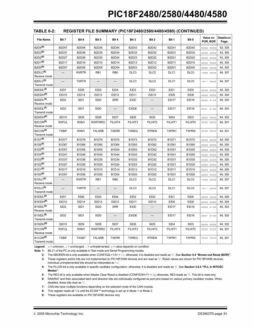
PIC18F2480/2580/4480/4580
B2D4(8) B2D47 B2D46 B2D45 B2D44 B2D43 B2D42 B2D41 B2D40 xxxx xxxx 63, 305
B2D3(8) B2D37 B2D36 B2D35 B2D34 B2D33 B2D32 B2D31 B2D30 xxxx xxxx 63, 305
B2D2(8) B2D27 B2D26 B2D25 B2D24 B2D23 B2D22 B2D21 B2D20 xxxx xxxx 63, 305
B2D1(8) B2D17 B2D16 B2D15 B2D14 B2D13 B2D12 B2D11 B2D10 xxxx xxxx 64, 305
B2D0(8) B2D07 B2D06 B2D05 B2D04 B2D03 B2D02 B2D01 B2D00 xxxx xxxx 64, 305
B2DLC(8) Receive mode
— RXRTR RB1 RB0 DLC3 DLC2 DLC1 DLC0 -xxx xxxx 64, 307
B2DLC(8) Transmit mode
— TXRTR — — DLC3 DLC2 DLC1 DLC0 -x-- xxxx 64, 307
B2EIDL(8) EID7 EID6 EID5 EID4 EID3 EID2 EID1 EID0 xxxx xxxx 64, 305
B2EIDH(8) EID15 EID14 EID13 EID12 EID11 EID10 EID9 EID8 xxxx xxxx 64, 304
B2SIDL(8) Receive mode
SID2 SID1 SID0 SRR EXID — EID17 EID16 xxxx x-xx 64, 303
B2SIDL(8) Transmit mode
SID2 SID1 SID0 — EXIDE — EID17 EID16 xxx- x-xx 64, 303
B2SIDH(8) SID10 SID9 SID8 SID7 SID6 SID5 SID4 SID3 xxxx xxxx 64, 302
B2CON(8) Receive mode
RXFUL RXM1 RXRTRRO FILHIT4 FILHIT3 FILHIT2 FILHIT1 FILHIT0 0000 0000 64, 301
B2CON(8) Transmit mode
TXBIF RXM1 TXLARB TXERR TXREQ RTREN TXPRI1 TXPRI0 0000 0000 64, 301
B1D7(8) B1D77 B1D76 B1D75 B1D74 B1D73 B1D72 B1D71 B1D70 xxxx xxxx 64, 305
B1D6(8) B1D67 B1D66 B1D65 B1D64 B1D63 B1D62 B1D61 B1D60 xxxx xxxx 64, 305
B1D5(8) B1D57 B1D56 B1D55 B1D54 B1D53 B1D52 B1D51 B1D50 xxxx xxxx 64, 305
B1D4(8) B1D47 B1D46 B1D45 B1D44 B1D43 B1D42 B1D41 B1D40 xxxx xxxx 64, 305
B1D3(8) B1D37 B1D36 B1D35 B1D34 B1D33 B1D32 B1D31 B1D30 xxxx xxxx 64, 305
B1D2(8) B1D27 B1D26 B1D25 B1D24 B1D23 B1D22 B1D21 B1D20 xxxx xxxx 64, 305
B1D1(8) B1D17 B1D16 B1D15 B1D14 B1D13 B1D12 B1D11 B1D10 xxxx xxxx 64, 305
B1D0(8) B1D07 B1D06 B1D05 B1D04 B1D03 B1D02 B1D01 B1D00 xxxx xxxx 64, 305
B1DLC(8) Receive mode
— RXRTR RB1 RB0 DLC3 DLC2 DLC1 DLC0 -xxx xxxx 64, 307
B1DLC(8) Transmit mode
— TXRTR — — DLC3 DLC2 DLC1 DLC0 -x-- xxxx 64, 307
B1EIDL(8) EID7 EID6 EID5 EID4 EID3 EID2 EID1 EID0 xxxx xxxx 64, 305
B1EIDH(8) EID15 EID14 EID13 EID12 EID11 EID10 EID9 EID8 xxxx xxxx 64, 304
B1SIDL(8) Receive mode
SID2 SID1 SID0 SRR EXID — EID17 EID16 xxxx x-xx 64, 303
B1SIDL(8) Transmit mode
SID2 SID1 SID0 — EXIDE — EID17 EID16 xxx- x-xx 64, 303
B1SIDH(8) SID10 SID9 SID8 SID7 SID6 SID5 SID4 SID3 xxxx xxxx 64, 302
B1CON(8) Receive mode
RXFUL RXM1 RXRTRRO FILHIT4 FILHIT3 FILHIT2 FILHIT1 FILHIT0 0000 0000 64, 301
B1CON(8) Transmit mode
TXBIF TXABT TXLARB TXERR TXREQ RTREN TXPRI1 TXPRI0 0000 0000 64, 301
TABLE 6-2: REGISTER FILE SUMMARY (PIC18F2480/2580/4480/4580) (CONTINUED)
File Name Bit 7 Bit 6 Bit 5 Bit 4 Bit 3 Bit 2 Bit 1 Bit 0 Value on POR, BOR
Details on Page:
Legend: x = unknown, u = unchanged, - = unimplemented, q = value depends on conditionNote 1: Bit 21 of the PC is only available in Test mode and Serial Programming modes.
2: The SBOREN bit is only available when CONFIG2L<1:0> = 01; otherwise, it is disabled and reads as ‘0’. See Section 5.4 “Brown-out Reset (BOR)”.3: These registers and/or bits are not implemented on PIC18F2X80 devices and are read as ‘0’. Reset values are shown for PIC18F4X80 devices;
individual unimplemented bits should be interpreted as ‘—’.4: The PLLEN bit is only available in specific oscillator configuration; otherwise, it is disabled and reads as ‘0’. See Section 3.6.4 “PLL in INTOSC
Modes”.5: The RE3 bit is only available when Master Clear Reset is disabled (CONFIG3H<7> = 0); otherwise, RE3 reads as ‘0’. This bit is read-only.6: RA6/RA7 and their associated latch and direction bits are individually configured as port pins based on various primary oscillator modes. When
disabled, these bits read as ‘0’.7: CAN bits have multiple functions depending on the selected mode of the CAN module.8: This register reads all ‘0’s until the ECAN™ technology is set up in Mode 1 or Mode 2.9: These registers are available on PIC18F4X80 devices only.
© 2009 Microchip Technology Inc. DS39637D-page 91

PIC18F2480/2580/4480/4580
B0D7(8) B0D77 B0D76 B0D75 B0D74 B0D73 B0D72 B0D71 B0D70 xxxx xxxx 64, 305
B0D6(8) B0D67 B0D66 B0D65 B0D64 B0D63 B0D62 B0D61 B0D60 xxxx xxxx 64, 305
B0D5(8) B0D57 B0D56 B0D55 B0D54 B0D53 B0D52 B0D51 B0D50 xxxx xxxx 64, 305
B0D4(8) B0D47 B0D46 B0D45 B0D44 B0D43 B0D42 B0D41 B0D40 xxxx xxxx 64, 305
B0D3(8) B0D37 B0D36 B0D35 B0D34 B0D33 B0D32 B0D31 B0D30 xxxx xxxx 64, 305
B0D2(8) B0D27 B0D26 B0D25 B0D24 B0D23 B0D22 B0D21 B0D20 xxxx xxxx 64, 305
B0D1(8) B0D17 B0D16 B0D15 B0D14 B0D13 B0D12 B0D11 B0D10 xxxx xxxx 64, 305
B0D0(8) B0D07 B0D06 B0D05 B0D04 B0D03 B0D02 B0D01 B0D00 xxxx xxxx 64, 305
B0DLC(8) Receive mode
— RXRTR RB1 RB0 DLC3 DLC2 DLC1 DLC0 -xxx xxxx 64, 307
B0DLC(8) Transmit mode
— TXRTR — — DLC3 DLC2 DLC1 DLC0 -x-- xxxx 64, 307
B0EIDL(8) EID7 EID6 EID5 EID4 EID3 EID2 EID1 EID0 xxxx xxxx 65, 305
B0EIDH(8) EID15 EID14 EID13 EID12 EID11 EID10 EID9 EID8 xxxx xxxx 65, 304
B0SIDL(8) Receive mode
SID2 SID1 SID0 SRR EXID — EID17 EID16 xxxx x-xx 65, 303
B0SIDL(8) Transmit mode
SID2 SID1 SID0 — EXIDE — EID17 EID16 xxx- x-xx 65, 303
B0SIDH(8) SID10 SID9 SID8 SID7 SID6 SID5 SID4 SID3 xxxx xxxx 65, 302
B0CON(8) Receive mode
RXFUL RXM1 RXRTRRO FILHIT4 FILHIT3 FILHIT2 FILHIT1 FILHIT0 0000 0000 64, 301
B0CON(8) Transmit mode
TXBIF TXABT TXLARB TXERR TXREQ RTREN TXPRI1 TXPRI0 0000 0000 64, 301
TXBIE — — — TXB2IE TXB1IE TXB0IE — — ---0 00-- 65, 324
BIE0 B5IE B4IE B3IE B2IE B1IE B0IE RXB1IE RXB0IE 0000 0000 65, 324
BSEL0 B5TXEN B4TXEN B3TXEN B2TXEN B1TXEN B0TXEN — — 0000 00-- 65, 307
MSEL3 FIL15_1 FIL15_0 FIL14_1 FIL14_0 FIL13_1 FIL13_0 FIL12_1 FIL12_0 0000 0000 65, 316
MSEL2 FIL11_1 FIL11_0 FIL10_1 FIL10_0 FIL9_1 FIL9_0 FIL8_1 FIL8_0 0000 0000 65, 315
MSEL1 FIL7_1 FIL7_0 FIL6_1 FIL6_0 FIL5_1 FIL5_0 FIL4_1 FIL4_0 0000 0101 65, 314
MSEL0 FIL3_1 FIL3_0 FIL2_1 FIL2_0 FIL1_1 FIL1_0 FIL0_1 FIL0_0 0101 0000 65, 313
RXFBCON7 F15BP_3 F15BP_2 F15BP_1 F15BP_0 F14BP_3 F14BP_2 F14BP_1 F14BP_0 0000 0000 65, 312
RXFBCON6 F13BP_3 F13BP_2 F13BP_1 F13BP_0 F12BP_3 F12BP_2 F12BP_1 F12BP_0 0000 0000 65, 312
RXFBCON5 F11BP_3 F11BP_2 F11BP_1 F11BP_0 F10BP_3 F10BP_2 F10BP_1 F10BP_0 0000 0000 65, 312
RXFBCON4 F9BP_3 F9BP_2 F9BP_1 F9BP_0 F8BP_3 F8BP_2 F8BP_1 F8BP_0 0000 0000 65, 312
RXFBCON3 F7BP_3 F7BP_2 F7BP_1 F7BP_0 F6BP_3 F6BP_2 F6BP_1 F6BP_0 0000 0000 65, 312
RXFBCON2 F5BP_3 F5BP_2 F5BP_1 F5BP_0 F4BP_3 F4BP_2 F4BP_1 F4BP_0 0001 0001 65, 312
RXFBCON1 F3BP_3 F3BP_2 F3BP_1 F3BP_0 F2BP_3 F2BP_2 F2BP_1 F2BP_0 0001 0001 65, 312
RXFBCON0 F1BP_3 F1BP_2 F1BP_1 F1BP_0 F0BP_3 F0BP_2 F0BP_1 F0BP_0 0000 0000 65, 312
SDFLC — — — FLC4 FLC3 FLC2 FLC1 FLC0 ---0 0000 65, 312
RXFCON1 RXF15EN RXF14EN RXF13EN RXF12EN RXF11EN RXF10EN RXF9EN RXF8EN 0000 0000 65, 311
RXFCON0 RXF7EN RXF6EN RXF5EN RXF4EN RXF3EN RXF2EN RXF1EN RXF0EN 0000 0000 65, 311
RXF15EIDL EID7 EID6 EID5 EID4 EID3 EID2 EID1 EID0 xxxx xxxx 65, 309
TABLE 6-2: REGISTER FILE SUMMARY (PIC18F2480/2580/4480/4580) (CONTINUED)
File Name Bit 7 Bit 6 Bit 5 Bit 4 Bit 3 Bit 2 Bit 1 Bit 0 Value on POR, BOR
Details on Page:
Legend: x = unknown, u = unchanged, - = unimplemented, q = value depends on conditionNote 1: Bit 21 of the PC is only available in Test mode and Serial Programming modes.
2: The SBOREN bit is only available when CONFIG2L<1:0> = 01; otherwise, it is disabled and reads as ‘0’. See Section 5.4 “Brown-out Reset (BOR)”.3: These registers and/or bits are not implemented on PIC18F2X80 devices and are read as ‘0’. Reset values are shown for PIC18F4X80 devices;
individual unimplemented bits should be interpreted as ‘—’.4: The PLLEN bit is only available in specific oscillator configuration; otherwise, it is disabled and reads as ‘0’. See Section 3.6.4 “PLL in INTOSC
Modes”.5: The RE3 bit is only available when Master Clear Reset is disabled (CONFIG3H<7> = 0); otherwise, RE3 reads as ‘0’. This bit is read-only.6: RA6/RA7 and their associated latch and direction bits are individually configured as port pins based on various primary oscillator modes. When
disabled, these bits read as ‘0’.7: CAN bits have multiple functions depending on the selected mode of the CAN module.8: This register reads all ‘0’s until the ECAN™ technology is set up in Mode 1 or Mode 2.9: These registers are available on PIC18F4X80 devices only.
DS39637D-page 92 © 2009 Microchip Technology Inc.
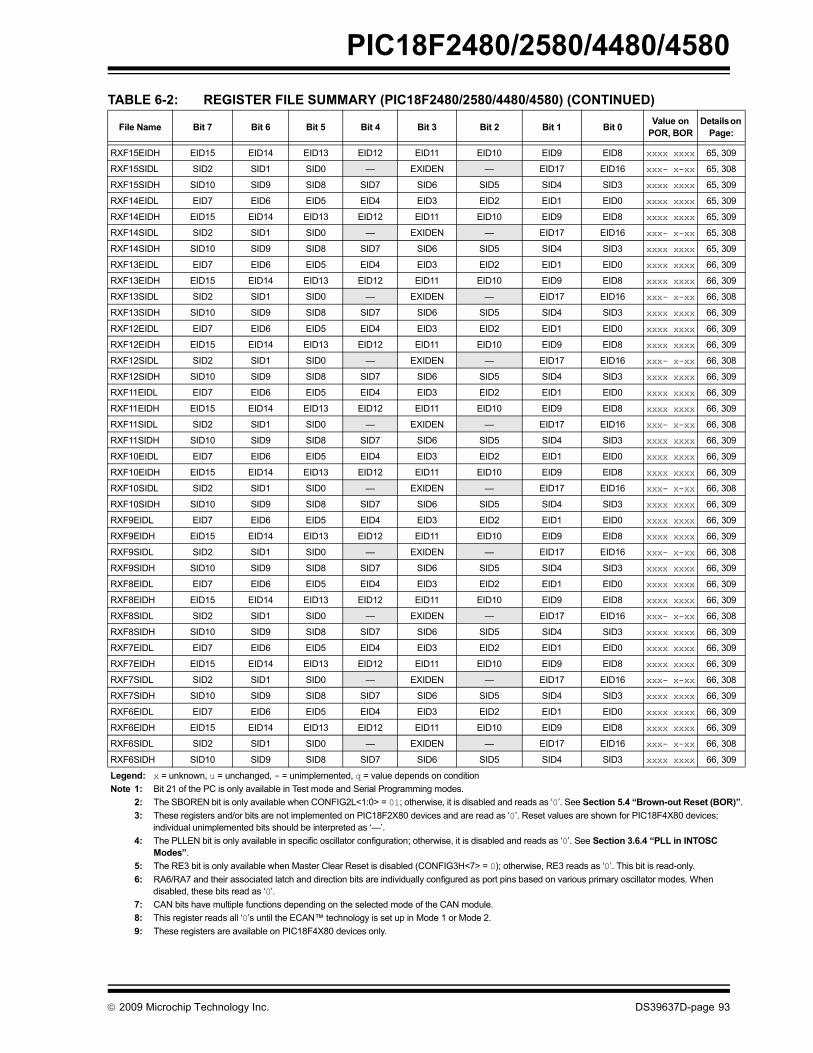
PIC18F2480/2580/4480/4580
RXF15EIDH EID15 EID14 EID13 EID12 EID11 EID10 EID9 EID8 xxxx xxxx 65, 309
RXF15SIDL SID2 SID1 SID0 — EXIDEN — EID17 EID16 xxx- x-xx 65, 308
RXF15SIDH SID10 SID9 SID8 SID7 SID6 SID5 SID4 SID3 xxxx xxxx 65, 309
RXF14EIDL EID7 EID6 EID5 EID4 EID3 EID2 EID1 EID0 xxxx xxxx 65, 309
RXF14EIDH EID15 EID14 EID13 EID12 EID11 EID10 EID9 EID8 xxxx xxxx 65, 309
RXF14SIDL SID2 SID1 SID0 — EXIDEN — EID17 EID16 xxx- x-xx 65, 308
RXF14SIDH SID10 SID9 SID8 SID7 SID6 SID5 SID4 SID3 xxxx xxxx 65, 309
RXF13EIDL EID7 EID6 EID5 EID4 EID3 EID2 EID1 EID0 xxxx xxxx 66, 309
RXF13EIDH EID15 EID14 EID13 EID12 EID11 EID10 EID9 EID8 xxxx xxxx 66, 309
RXF13SIDL SID2 SID1 SID0 — EXIDEN — EID17 EID16 xxx- x-xx 66, 308
RXF13SIDH SID10 SID9 SID8 SID7 SID6 SID5 SID4 SID3 xxxx xxxx 66, 309
RXF12EIDL EID7 EID6 EID5 EID4 EID3 EID2 EID1 EID0 xxxx xxxx 66, 309
RXF12EIDH EID15 EID14 EID13 EID12 EID11 EID10 EID9 EID8 xxxx xxxx 66, 309
RXF12SIDL SID2 SID1 SID0 — EXIDEN — EID17 EID16 xxx- x-xx 66, 308
RXF12SIDH SID10 SID9 SID8 SID7 SID6 SID5 SID4 SID3 xxxx xxxx 66, 309
RXF11EIDL EID7 EID6 EID5 EID4 EID3 EID2 EID1 EID0 xxxx xxxx 66, 309
RXF11EIDH EID15 EID14 EID13 EID12 EID11 EID10 EID9 EID8 xxxx xxxx 66, 309
RXF11SIDL SID2 SID1 SID0 — EXIDEN — EID17 EID16 xxx- x-xx 66, 308
RXF11SIDH SID10 SID9 SID8 SID7 SID6 SID5 SID4 SID3 xxxx xxxx 66, 309
RXF10EIDL EID7 EID6 EID5 EID4 EID3 EID2 EID1 EID0 xxxx xxxx 66, 309
RXF10EIDH EID15 EID14 EID13 EID12 EID11 EID10 EID9 EID8 xxxx xxxx 66, 309
RXF10SIDL SID2 SID1 SID0 — EXIDEN — EID17 EID16 xxx- x-xx 66, 308
RXF10SIDH SID10 SID9 SID8 SID7 SID6 SID5 SID4 SID3 xxxx xxxx 66, 309
RXF9EIDL EID7 EID6 EID5 EID4 EID3 EID2 EID1 EID0 xxxx xxxx 66, 309
RXF9EIDH EID15 EID14 EID13 EID12 EID11 EID10 EID9 EID8 xxxx xxxx 66, 309
RXF9SIDL SID2 SID1 SID0 — EXIDEN — EID17 EID16 xxx- x-xx 66, 308
RXF9SIDH SID10 SID9 SID8 SID7 SID6 SID5 SID4 SID3 xxxx xxxx 66, 309
RXF8EIDL EID7 EID6 EID5 EID4 EID3 EID2 EID1 EID0 xxxx xxxx 66, 309
RXF8EIDH EID15 EID14 EID13 EID12 EID11 EID10 EID9 EID8 xxxx xxxx 66, 309
RXF8SIDL SID2 SID1 SID0 — EXIDEN — EID17 EID16 xxx- x-xx 66, 308
RXF8SIDH SID10 SID9 SID8 SID7 SID6 SID5 SID4 SID3 xxxx xxxx 66, 309
RXF7EIDL EID7 EID6 EID5 EID4 EID3 EID2 EID1 EID0 xxxx xxxx 66, 309
RXF7EIDH EID15 EID14 EID13 EID12 EID11 EID10 EID9 EID8 xxxx xxxx 66, 309
RXF7SIDL SID2 SID1 SID0 — EXIDEN — EID17 EID16 xxx- x-xx 66, 308
RXF7SIDH SID10 SID9 SID8 SID7 SID6 SID5 SID4 SID3 xxxx xxxx 66, 309
RXF6EIDL EID7 EID6 EID5 EID4 EID3 EID2 EID1 EID0 xxxx xxxx 66, 309
RXF6EIDH EID15 EID14 EID13 EID12 EID11 EID10 EID9 EID8 xxxx xxxx 66, 309
RXF6SIDL SID2 SID1 SID0 — EXIDEN — EID17 EID16 xxx- x-xx 66, 308
RXF6SIDH SID10 SID9 SID8 SID7 SID6 SID5 SID4 SID3 xxxx xxxx 66, 309
TABLE 6-2: REGISTER FILE SUMMARY (PIC18F2480/2580/4480/4580) (CONTINUED)
File Name Bit 7 Bit 6 Bit 5 Bit 4 Bit 3 Bit 2 Bit 1 Bit 0 Value on POR, BOR
Details on Page:
Legend: x = unknown, u = unchanged, - = unimplemented, q = value depends on conditionNote 1: Bit 21 of the PC is only available in Test mode and Serial Programming modes.
2: The SBOREN bit is only available when CONFIG2L<1:0> = 01; otherwise, it is disabled and reads as ‘0’. See Section 5.4 “Brown-out Reset (BOR)”.3: These registers and/or bits are not implemented on PIC18F2X80 devices and are read as ‘0’. Reset values are shown for PIC18F4X80 devices;
individual unimplemented bits should be interpreted as ‘—’.4: The PLLEN bit is only available in specific oscillator configuration; otherwise, it is disabled and reads as ‘0’. See Section 3.6.4 “PLL in INTOSC
Modes”.5: The RE3 bit is only available when Master Clear Reset is disabled (CONFIG3H<7> = 0); otherwise, RE3 reads as ‘0’. This bit is read-only.6: RA6/RA7 and their associated latch and direction bits are individually configured as port pins based on various primary oscillator modes. When
disabled, these bits read as ‘0’.7: CAN bits have multiple functions depending on the selected mode of the CAN module.8: This register reads all ‘0’s until the ECAN™ technology is set up in Mode 1 or Mode 2.9: These registers are available on PIC18F4X80 devices only.
© 2009 Microchip Technology Inc. DS39637D-page 93

PIC18F2480/2580/4480/4580
6.3.5 STATUS REGISTERThe STATUS register, shown in Register 6-2, containsthe arithmetic status of the ALU. As with any other SFR,it can be the operand for any instruction.If the STATUS register is the destination for an instruc-tion that affects the Z, DC, C, OV or N bits, the resultsof the instruction are not written; instead, the status isupdated according to the instruction performed. There-fore, the result of an instruction with the STATUSregister as its destination may be different thanintended. As an example, CLRF STATUS will set the Zbit and leave the remaining Status bits unchanged(‘000u u1uu’).
It is recommended that only BCF, BSF, SWAPF, MOVFFand MOVWF instructions are used to alter the STATUSregister, because these instructions do not affect the Z,C, DC, OV or N bits in the STATUS register.
For other instructions that do not affect Status bits, seethe instruction set summaries in Table 26-2 andTable 26-3.
Note: The C and DC bits operate as the borrowand digit borrow bits respectively insubtraction.
REGISTER 6-2: STATUS REGISTER
U-0 U-0 U-0 R/W-x R/W-x R/W-x R/W-x R/W-x— — — N OV Z DC(1) C(2)
bit 7 bit 0
Legend:R = Readable bit W = Writable bit U = Unimplemented bit, read as ‘0’-n = Value at POR ‘1’ = Bit is set ‘0’ = Bit is cleared x = Bit is unknown
bit 7-5 Unimplemented: Read as ‘0’bit 4 N: Negative bit
This bit is used for signed arithmetic (2’s complement). It indicates whether the result was negative (ALU MSB = 1).1 = Result was negative 0 = Result was positive
bit 3 OV: Overflow bit This bit is used for signed arithmetic (2’s complement). It indicates an overflow of the 7-bit magnitude which causes the sign bit (bit 7) to change state.1 = Overflow occurred for signed arithmetic (in this arithmetic operation) 0 = No overflow occurred
bit 2 Z: Zero bit 1 = The result of an arithmetic or logic operation is zero 0 = The result of an arithmetic or logic operation is not zero
bit 1 DC: Digit carry/borrow bit(1) For ADDWF, ADDLW, SUBLW and SUBWF instructions: 1 = A carry-out from the 4th low-order bit of the result occurred 0 = No carry-out from the 4th low-order bit of the result
bit 0 C: Carry/borrow bit(2) For ADDWF, ADDLW, SUBLW and SUBWF instructions: 1 = A carry-out from the Most Significant bit of the result occurred 0 = No carry-out from the Most Significant bit of the result occurred
Note 1: For borrow, the polarity is reversed. A subtraction is executed by adding the two’s complement of the second operand. For rotate (RRF, RLF) instructions, this bit is loaded with either the bit 4 or bit 3 of the source register.
2: For borrow, the polarity is reversed. A subtraction is executed by adding the two’s complement of the second operand. For rotate (RRF, RLF) instructions, this bit is loaded with either the high or low-order bit of the source register.
DS39637D-page 94 © 2009 Microchip Technology Inc.

PIC18F2480/2580/4480/4580
6.4 Data Addressing ModesWhile the program memory can be addressed in onlyone way – through the program counter – informationin the data memory space can be addressed in severalways. For most instructions, the addressing mode isfixed. Other instructions may use up to three modes,depending on which operands are used and whether ornot the extended instruction set is enabled.
The addressing modes are:
• Inherent• Literal• Direct• Indirect
An additional addressing mode, Indexed Literal Offset,is available when the extended instruction set isenabled (XINST Configuration bit = 1). Its operation isdiscussed in greater detail in Section 6.6.1 “IndexedAddressing with Literal Offset”.
6.4.1 INHERENT AND LITERAL ADDRESSING
Many PIC18 control instructions do not need anyargument at all; they either perform an operation thatglobally affects the device or they operate implicitly onone register. This addressing mode is known asInherent Addressing. Examples include SLEEP, RESETand DAW.
Other instructions work in a similar way but require anadditional explicit argument in the opcode. This isknown as Literal Addressing mode because theyrequire some literal value as an argument. Examplesinclude ADDLW and MOVLW which, respectively, add ormove a literal value to the W register. Other examplesinclude CALL and GOTO, which include a 20-bitprogram memory address.
6.4.2 DIRECT ADDRESSINGDirect Addressing specifies all or part of the sourceand/or destination address of the operation within theopcode itself. The options are specified by thearguments accompanying the instruction.
In the core PIC18 instruction set, bit-oriented andbyte-oriented instructions use some version of DirectAddressing by default. All of these instructions includesome 8-bit literal address as their Least SignificantByte. This address specifies either a register address inone of the banks of data RAM (Section 6.3.3 “General
Purpose Register File”) or a location in the AccessBank (Section 6.3.2 “Access Bank”) as the datasource for the instruction.
The Access RAM bit ‘a’ determines how the address isinterpreted. When ‘a’ is ‘1’, the contents of the BSR(Section 6.3.1 “Bank Select Register (BSR)”) areused with the address to determine the complete 12-bitaddress of the register. When ‘a’ is ‘0’, the address isinterpreted as being a register in the Access Bank.Addressing that uses the Access RAM is sometimesalso known as Direct Forced Addressing mode.
A few instructions, such as MOVFF, include the entire12-bit address (either source or destination) in theiropcodes. In these cases, the BSR is ignored entirely.
The destination of the operation’s results is determinedby the destination bit, ‘d’. When ‘d’ is ‘1’, the results arestored back in the source register, overwriting its origi-nal contents. When ‘d’ is ‘0’, the results are stored inthe W register. Instructions without the ‘d’ argumenthave a destination that is implicit in the instruction; theirdestination is either the target register being operatedon or the W register.
6.4.3 INDIRECT ADDRESSINGIndirect Addressing allows the user to access a locationin data memory without giving a fixed address in theinstruction. This is done by using File Select Registers(FSRs) as pointers to the locations to be read or writtento. Since the FSRs are themselves located in RAM asSpecial File Registers, they can also be directly manip-ulated under program control. This makes FSRs veryuseful in implementing data structures, such as tablesand arrays in data memory.
The registers for Indirect Addressing are also imple-mented with Indirect File Operands (INDFs) that permitautomatic manipulation of the pointer value withauto-incrementing, auto-decrementing or offsettingwith another value. This allows for efficient code, usingloops, such as the example of clearing an entire RAMbank in Example 6-5.
EXAMPLE 6-5: HOW TO CLEAR RAM (BANK 1) USING INDIRECT ADDRESSING
Note: The execution of some instructions in thecore PIC18 instruction set are changedwhen the PIC18 extended instructionset is enabled. See Section 6.6 “DataMemory and the Extended InstructionSet” for more information.
LFSR FSR0, 100h ; NEXT CLRF POSTINC0 ; Clear INDF
; register then ; inc pointer
BTFSS FSR0H,1 ; All done with; Bank1?
BRA NEXT ; NO, clear next CONTINUE ; YES, continue
© 2009 Microchip Technology Inc. DS39637D-page 95

PIC18F2480/2580/4480/4580
6.4.3.1 FSR Registers and theINDF OperandAt the core of Indirect Addressing are three sets ofregisters: FSR0, FSR1 and FSR2. Each represents apair of 8-bit registers, FSRnH and FSRnL. The fourupper bits of the FSRnH register are not used, so eachFSR pair holds a 12-bit value. This represents a valuethat can address the entire range of the data memoryin a linear fashion. The FSR register pairs, then, serveas pointers to data memory locations.
Indirect Addressing is accomplished with a set ofIndirect File Operands, INDF0 through INDF2. Thesecan be thought of as “virtual” registers: they are
mapped in the SFR space, but are not physically imple-mented. Reading or writing to a particular INDF registeractually accesses its corresponding FSR register pair.A read from INDF1, for example, reads the data at theaddress indicated by FSR1H:FSR1L. Instructions thatuse the INDF registers as operands actually use thecontents of their corresponding FSR as a pointer to theinstruction’s target. The INDF operand is just aconvenient way of using the pointer.
Because Indirect Addressing uses a full 12-bit address,data RAM banking is not necessary. Thus, the currentcontents of the BSR and the Access RAM bit have noeffect on determining the target address.
FIGURE 6-8: INDIRECT ADDRESSING
FSR1H:FSR1L
07
Data Memory
000h
100h
200h
300h
F00h
E00h
FFFh
Bank 0
Bank 1
Bank 2
Bank 14
Bank 15
Bank 3throughBank 13
ADDWF, INDF1, 1
07
Using an instruction with one of theIndirect Addressing registers as theoperand....
...uses the 12-bit address stored inthe FSR pair associated with thatregister....
...to determine the data memorylocation to be used in that operation.
In this case, the FSR1 pair containsECCh. This means the contents oflocation ECCh will be added to thatof the W register and stored back inECCh.
x x x x 1 1 1 0 1 1 0 0 1 1 0 0
Bank 14
DS39637D-page 96 © 2009 Microchip Technology Inc.

PIC18F2480/2580/4480/4580
6.4.3.2 FSR Registers and POSTINC,POSTDEC, PREINC and PLUSWIn addition to the INDF operand, each FSR register pairalso has four additional indirect operands. Like INDF,these are “virtual” registers that cannot be indirectlyread or written to. Accessing these registers actuallyaccesses the associated FSR register pair, but alsoperforms a specific action on its stored value. They are:
• POSTDEC: accesses the FSR value, then automatically decrements it by 1 afterwards
• POSTINC: accesses the FSR value, then automatically increments it by 1 afterwards
• PREINC: increments the FSR value by 1, then uses it in the operation
• PLUSW: adds the signed value of the W register (range of -127 to 128) to that of the FSR and uses the new value in the operation.
In this context, accessing an INDF register, uses thevalue in the FSR registers without changing them.Similarly, accessing a PLUSW register gives the FSRvalue offset by that in the W register; neither value isactually changed in the operation. Accessing the othervirtual registers changes the value of the FSRregisters.
Operations on the FSRs with POSTDEC, POSTINCand PREINC affect the entire register pair; that is, roll-overs of the FSRnL register from FFh to 00h carry overto the FSRnH register. On the other hand, results ofthese operations do not change the value of any flagsin the STATUS register (e.g., Z, N, OV, etc.).
The PLUSW register can be used to implement a formof Indexed Addressing in the data memory space. Bymanipulating the value in the W register, users canreach addresses that are fixed offsets from pointeraddresses. In some applications, this can be used toimplement some powerful program control structure,such as software stacks, inside of data memory.
6.4.3.3 Operations by FSRs on FSRsIndirect Addressing operations that target other FSRsor virtual registers represent special cases. Forexample, using an FSR to point to one of the virtualregisters will not result in successful operations. As aspecific case, assume that FSR0H:FSR0L containsFE7h, the address of INDF1. Attempts to read thevalue of the INDF1 using INDF0 as an operand willreturn 00h. Attempts to write to INDF1 using INDF0 asthe operand will result in a NOP.
On the other hand, using the virtual registers to write toan FSR pair may not occur as planned. In these cases,the value will be written to the FSR pair but without anyincrementing or decrementing. Thus, writing to INDF2or POSTDEC2 will write the same value to theFSR2H:FSR2L.
Since the FSRs are physical registers mapped in theSFR space, they can be manipulated through all directoperations. Users should proceed cautiously whenworking on these registers, particularly if their codeuses Indirect Addressing.
Similarly, operations by Indirect Addressing are gener-ally permitted on all other SFRs. Users should exercisethe appropriate caution that they do not inadvertentlychange settings that might affect the operation of thedevice.
© 2009 Microchip Technology Inc. DS39637D-page 97

PIC18F2480/2580/4480/4580
6.5 Program Memory and theExtended Instruction SetThe operation of program memory is unaffected by theuse of the extended instruction set.
Enabling the extended instruction set adds eightadditional two-word commands to the existingPIC18 instruction set: ADDFSR, ADDULNK, CALLW,MOVSF, MOVSS, PUSHL, SUBFSR and SUBULNK. Theseinstructions are executed as described inSection 6.2.4 “Two-Word Instructions”.
6.6 Data Memory and the Extended Instruction Set
Enabling the PIC18 extended instruction set (XINSTConfiguration bit = 1) significantly changes certainaspects of data memory and its addressing. Specifically,the use of the Access Bank for many of the core PIC18instructions is different. This is due to the introduction ofa new addressing mode for the data memory space. Thismode also alters the behavior of Indirect Addressingusing FSR2 and its associated operands.
What does not change is just as important. The size ofthe data memory space is unchanged, as well as itslinear addressing. The SFR map remains the same.Core PIC18 instructions can still operate in both Directand Indirect Addressing mode; inherent and literalinstructions do not change at all. Indirect Addressingwith FSR0 and FSR1 also remains unchanged.
6.6.1 INDEXED ADDRESSING WITH LITERAL OFFSET
Enabling the PIC18 extended instruction set changesthe behavior of Indirect Addressing using the FSR2register pair and its associated file operands. Under theproper conditions, instructions that use the AccessBank – that is, most bit-oriented and byte-oriented –instructions – can invoke a form of Indexed Addressingusing an offset specified in the instruction. This specialaddressing mode is known as Indexed Addressing withLiteral Offset or Indexed Literal Offset mode.
When using the extended instruction set, thisaddressing mode requires the following:
• The use of the Access Bank is forced (‘a’ = 0); and
• The file address argument is less than or equal to 5Fh.
Under these conditions, the file address of the instruc-tion is not interpreted as the lower byte of an address(used with the BSR in Direct Addressing), or as an 8-bitaddress in the Access Bank. Instead, the value isinterpreted as an offset value to an Address Pointer,specified by FSR2. The offset and the contents ofFSR2 are added to obtain the target address of theoperation.
6.6.2 INSTRUCTIONS AFFECTED BY INDEXED LITERAL OFFSET MODE
Any of the core PIC18 instructions that can use DirectAddressing are potentially affected by the IndexedLiteral Offset Addressing mode. This includes allbyte-oriented and bit-oriented instructions, or almostone-half of the standard PIC18 instruction set. Instruc-tions that only use Inherent or Literal Addressingmodes are unaffected.
Additionally, byte-oriented and bit-oriented instructionsare not affected if they use the Access Bank (AccessRAM bit is ‘1’), or include a file address of 60h or above.Instructions meeting these criteria will continue toexecute as before. A comparison of the differentpossible addressing modes when the extendedinstruction set is enabled in shown in Figure 6-9.
Those who desire to use byte-oriented or bit-orientedinstructions in the Indexed Literal Offset mode shouldnote the changes to assembler syntax for this mode.This is described in more detail in Section 26.2.1“Extended Instruction Syntax”.
DS39637D-page 98 © 2009 Microchip Technology Inc.

PIC18F2480/2580/4480/4580
FIGURE 6-9: COMPARING ADDRESSING OPTIONS FOR BIT-ORIENTED ANDBYTE-ORIENTED INSTRUCTIONS (EXTENDED INSTRUCTION SET ENABLED)
EXAMPLE INSTRUCTION: ADDWF, f, d, a (Opcode: 0010 01da ffff ffff)
When a = 0 and f ≥ 60h:The instruction executes inDirect Forced mode. ‘f’ is inter-preted as a location in theAccess RAM between 060hand 0FFh. This is the same asthe SFRs, or locations F60h to0FFh (Bank 15) of datamemory.
Locations below 60h are notavailable in this addressingmode.
When a = 0 and f ≤ 5Fh:The instruction executes inIndexed Literal Offset mode. ‘f’is interpreted as an offset to theaddress value in FSR2. Thetwo are added together toobtain the address of the targetregister for the instruction. Theaddress can be anywhere inthe data memory space.
Note that in this mode, thecorrect syntax is now:ADDWF [k], dwhere ‘k’ is the same as ‘f’.
When a = 1 (all values of f):The instruction executes inDirect mode (also known asDirect Long mode). ‘f’ isinterpreted as a location inone of the 16 banks of the datamemory space. The bank isdesignated by the Bank SelectRegister (BSR). The addresscan be in any implementedbank in the data memoryspace.
000h
060h
100h
F00h
F60h
FFFh
Valid range
00h
60h
FFh
Data Memory
Access RAM
Bank 0
Bank 1throughBank 14
Bank 15
SFRs
000h
080h
100h
F00h
F60h
FFFhData Memory
Bank 0
Bank 1throughBank 14
Bank 15
SFRs
FSR2H FSR2L
ffffffff001001da
ffffffff001001da
000h
080h
100h
F00h
F60h
FFFhData Memory
Bank 0
Bank 1throughBank 14
Bank 15
SFRs
for ‘f’
BSR00000000
080h
© 2009 Microchip Technology Inc. DS39637D-page 99

PIC18F2480/2580/4480/4580
6.6.3 MAPPING THE ACCESS BANK ININDEXED LITERAL OFFSET MODEThe use of Indexed Literal Offset Addressing modeeffectively changes how the lower half of Access RAM(00h to 7Fh) is mapped. Rather than containing just thecontents of the bottom half of Bank 0, this mode mapsthe contents from Bank 0 and a user-defined “window”that can be located anywhere in the data memoryspace. The value of FSR2 establishes the lower bound-ary of the addresses mapped into the window, while theupper boundary is defined by FSR2 plus 95 (5Fh).Addresses in the Access RAM above 5Fh are mappedas previously described (see Section 6.3.2 “AccessBank”). An example of Access Bank remapping in thisaddressing mode is shown in Figure 6-10.
Remapping of the Access Bank applies only to opera-tions using the Indexed Literal Offset mode. Operationsthat use the BSR (Access RAM bit is ‘1’) will continueto use Direct Addressing as before. Any indirect orindexed operation that explicitly uses any of the indirectfile operands (including FSR2) will continue to operateas standard Indirect Addressing. Any instruction thatuses the Access Bank, but includes a register addressof greater than 05Fh, will use Direct Addressing andthe normal Access Bank map.
6.6.4 BSR IN INDEXED LITERAL OFFSET MODE
Although the Access Bank is remapped when theextended instruction set is enabled, the operation of theBSR remains unchanged. Direct Addressing using theBSR to select the data memory bank operates in thesame manner as previously described.
FIGURE 6-10: REMAPPING THE ACCESS BANK WITH INDEXED LITERAL OFFSET ADDRESSING
Data Memory
000h
100h
200h
F60h
F00h
FFFh
Bank 1
Bank 15
Bank 2throughBank 14
SFRs
ADDWF f, d, aFSR2H:FSR2L = 120h
Locations in the regionfrom the FSR2 Pointer(120h) to the pointer plus05Fh (17Fh) are mappedto the bottom of theAccess RAM (000h-05Fh).
Special File Registers atF60h through FFFh aremapped to 60h throughFFh, as usual.
Bank 0 addresses below5Fh are not available inthis mode. They can stillbe addressed by using theBSR.
Access Bank
00h
60h
FFh
Bank 0
SFRs
Bank 1 “Window”
Window
Example Situation:
120h17Fh
5Fh
DS39637D-page 100 © 2009 Microchip Technology Inc.

PIC18F2480/2580/4480/4580
7.0 FLASH PROGRAM MEMORYThe Flash program memory is readable, writable anderasable, during normal operation over the entire VDDrange.
A read from program memory is executed on one byteat a time. A write to program memory is executed onblocks of 8 bytes at a time. Program memory is erasedin blocks of 64 bytes at a time. A bulk erase operationmay not be issued from user code.
Writing or erasing program memory will ceaseinstruction fetches until the operation is complete. Theprogram memory cannot be accessed during the writeor erase, therefore, code cannot execute. An internalprogramming timer terminates program memory writesand erases.
7.1 Table Reads and Table WritesIn order to read and write program memory, there aretwo operations that allow the processor to move bytesbetween the program memory space and the data RAM:
• Table Read (TBLRD)• Table Write (TBLWT)
The program memory space is 16 bits wide, while thedata RAM space is 8 bits wide. Table reads and tablewrites move data between these two memory spacesthrough an 8-bit register (TABLAT).
Table read operations retrieve data from programmemory and place it into the data RAM space.Figure 7-1 shows the operation of a table read withprogram memory and data RAM.
Table write operations store data from the data memoryspace into holding registers in program memory. Theprocedure to write the contents of the holding registersinto program memory is detailed in Section 7.5 “Writingto Flash Program Memory”. Figure 7-2 shows theoperation of a table write with program memory and dataRAM.
Table operations work with byte entities. A table blockcontaining data, rather than program instructions, is notrequired to be word aligned. Therefore, a table block canstart and end at any byte address. If a table write is beingused to write executable code into program memory,program instructions will need to be word aligned.
FIGURE 7-1: TABLE READ OPERATION
Table Pointer(1)Table Latch (8-bit)
Program Memory
TBLPTRH TBLPTRLTABLAT
TBLPTRU
Instruction: TBLRD*
Note 1: Table Pointer register points to a byte in program memory.
Program Memory(TBLPTR)
© 2009 Microchip Technology Inc. DS39637D-page 101

PIC18F2480/2580/4480/4580
FIGURE 7-2: TABLE WRITE OPERATION7.2 Control RegistersSeveral control registers are used in conjunction withthe TBLRD and TBLWT instructions. These include the:
• EECON1 register• EECON2 register• TABLAT register• TBLPTR registers
7.2.1 EECON1 AND EECON2 REGISTERSThe EECON1 register (Register 7-1) is the controlregister for memory accesses. The EECON2 register isnot a physical register; it is used exclusively in thememory write and erase sequences. ReadingEECON2 will read all ‘0’s.
The EEPGD control bit determines if the access will bea program or data EEPROM memory access. Whenclear, any subsequent operations will operate on thedata EEPROM memory. When set, any subsequentoperations will operate on the program memory.
The CFGS control bit determines if the access will beto the Configuration/Calibration registers or to programmemory/data EEPROM memory. When set,subsequent operations will operate on Configurationregisters regardless of EEPGD (see Section 25.0“Special Features of the CPU”). When clear, memoryselection access is determined by EEPGD.
The FREE bit, when set, will allow a program memoryerase operation. When FREE is set, the erase opera-tion is initiated on the next WR command. When FREEis clear, only writes are enabled.
The WREN bit, when set, will allow a write operation.On power-up, the WREN bit is clear. The WRERR bit isset in hardware when the WREN bit is set and clearedwhen the internal programming timer expires and thewrite operation is complete.
The WR control bit initiates write operations. The bitcannot be cleared, only set, in software; it is cleared inhardware at the completion of the write operation.
Table Pointer(1) Table Latch (8-bit)
TBLPTRH TBLPTRL TABLAT
Program Memory(TBLPTR)
TBLPTRU
Instruction: TBLWT*
Note 1: Table Pointer actually points to one of 32 holding registers, the address of which is determined byTBLPTRL<4:0>. The process for physically writing data to the program memory array is discussed inSection 7.5 “Writing to Flash Program Memory”.
Holding Registers Program Memory
Note: During normal operation, the WRERR isread as ‘1’. This can indicate that a writeoperation was prematurely terminated bya Reset, or a write operation wasattempted improperly.
Note: The EEIF Interrupt Flag bit (PIR2<4>) isset when the write is complete. It must becleared in software.
DS39637D-page 102 © 2009 Microchip Technology Inc.

PIC18F2480/2580/4480/4580
REGISTER 7-1: EECON1: DATA EEPROM CONTROL REGISTER 1R/W-x R/W-x U-0 R/W-0 R/W-x R/W-0 R/S-0 R/S-0EEPGD CFGS — FREE WRERR(1) WREN WR RD
bit 7 bit 0
Legend: S = Settable bitR = Readable bit W = Writable bit U = Unimplemented bit, read as ‘0’-n = Value at POR ‘1’ = Bit is set ‘0’ = Bit is cleared x = Bit is unknown
bit 7 EEPGD: Flash Program or Data EEPROM Memory Select bit1 = Access Flash program memory0 = Access data EEPROM memory
bit 6 CFGS: Flash Program/Data EEPROM or Configuration Select bit1 = Access Configuration registers0 = Access Flash program or data EEPROM memory
bit 5 Unimplemented: Read as ‘0’bit 4 FREE: Flash Row Erase Enable bit
1 = Erase the program memory row addressed by TBLPTR on the next WR command (cleared bycompletion of erase operation)
0 = Perform write onlybit 3 WRERR: Flash Program/Data EEPROM Error Flag bit(1)
1 = A write operation is prematurely terminated (any Reset during self-timed programming in normaloperation or an improper write attempt)
0 = The write operation completedbit 2 WREN: Flash Program/Data EEPROM Write Enable bit
1 = Allows write cycles to Flash program/data EEPROM0 = Inhibits write cycles to Flash program/data EEPROM
bit 1 WR: Write Control bit1 = Initiates a data EEPROM erase/write cycle or a program memory erase cycle or write cycle
(The operation is self-timed and the bit is cleared by hardware once write is complete. The WR bit can only be set (not cleared) in software.)
0 = Write cycle to the EEPROM is completebit 0 RD: Read Control bit
1 = Initiates an EEPROM read (Read takes one cycle. RD is cleared in hardware. The RD bit can onlybe set (not cleared) in software. RD bit cannot be set when EEPGD = 1 or CFGS = 1.)
0 = Does not initiate an EEPROM read
Note 1: When a WRERR occurs, the EEPGD and CFGS bits are not cleared. This allows tracing of the error condition.
© 2009 Microchip Technology Inc. DS39637D-page 103

PIC18F2480/2580/4480/4580
7.2.2 TABLAT – TABLE LATCH REGISTERThe Table Latch (TABLAT) is an 8-bit register mappedinto the SFR space. The Table Latch register is used tohold 8-bit data during data transfers between programmemory and data RAM.7.2.3 TBLPTR – TABLE POINTER REGISTER
The Table Pointer (TBLPTR) register addresses a bytewithin the program memory. The TBLPTR is comprisedof three SFR registers: Table Pointer Upper Byte, TablePointer High Byte and Table Pointer Low Byte(TBLPTRU:TBLPTRH:TBLPTRL). These three regis-ters join to form a 22-bit wide pointer. The low-order21 bits allow the device to address up to 2 Mbytes ofprogram memory space. The 22nd bit allows access tothe Device ID, the user ID and the Configuration bits.
The Table Pointer, TBLPTR, is used by the TBLRD andTBLWT instructions. These instructions can update theTBLPTR in one of four ways based on the table opera-tion. These operations are shown in Table 7-1. Theseoperations on the TBLPTR only affect the low-order21 bits.
7.2.4 TABLE POINTER BOUNDARIESTBLPTR is used in reads, writes and erases of theFlash program memory.
When a TBLRD is executed, all 22 bits of the TBLPTRdetermine which byte is read from program memoryinto TABLAT.
When a TBLWT is executed, the five LSbs of the TablePointer register (TBLPTR<4:0>) determine which ofthe 32 program memory holding registers is written to.When the timed write to program memory begins (viathe WR bit), the 16 MSbs of the TBLPTR(TBLPTR<21:6>) determine which program memoryblock of 32 bytes is written to. For more detail, seeSection 7.5 “Writing to Flash Program Memory”.
When an erase of program memory is executed, the16 MSbs of the Table Pointer register (TBLPTR<21:6>)point to the 64-byte block that will be erased. The LeastSignificant bits (TBLPTR<5:0>) are ignored.
Figure 7-3 describes the relevant boundaries ofTBLPTR based on Flash program memory operations.
TABLE 7-1: TABLE POINTER OPERATIONS WITH TBLRD AND TBLWT INSTRUCTIONS
FIGURE 7-3: TABLE POINTER BOUNDARIES BASED ON OPERATION
Example Operation on Table Pointer
TBLRD*TBLWT*
TBLPTR is not modified
TBLRD*+TBLWT*+
TBLPTR is incremented after the read/write
TBLRD*-TBLWT*-
TBLPTR is decremented after the read/write
TBLRD+*TBLWT+*
TBLPTR is incremented before the read/write
21 16 15 8 7 0
TABLE ERASE/WRITE TABLE WRITE
TABLE READ – TBLPTR<21:0>
TBLPTRLTBLPTRHTBLPTRU
TBLPTR<5:0>TBLPTR<21:6>
DS39637D-page 104 © 2009 Microchip Technology Inc.

PIC18F2480/2580/4480/4580
7.3 Reading the Flash ProgramMemoryThe TBLRD instruction is used to retrieve data fromprogram memory and place it into data RAM. Tablereads from program memory are performed one byte ata time.
TBLPTR points to a byte address in program space.Executing TBLRD places the byte pointed to intoTABLAT. In addition, TBLPTR can be modifiedautomatically for the next table read operation.
The internal program memory is typically organized bywords. The Least Significant bit of the address selectsbetween the high and low bytes of the word. Figure 7-4shows the interface between the internal programmemory and the TABLAT.
FIGURE 7-4: READS FROM FLASH PROGRAM MEMORY
EXAMPLE 7-1: READING A FLASH PROGRAM MEMORY WORD
(Even Byte Address)
Program Memory
(Odd Byte Address)
TBLRD TABLAT
TBLPTR = xxxxx1
FETCHInstruction Register (IR) Read Register
TBLPTR = xxxxx0
MOVLW CODE_ADDR_UPPER ; Load TBLPTR with the baseMOVWF TBLPTRU ; address of the wordMOVLW CODE_ADDR_HIGHMOVWF TBLPTRHMOVLW CODE_ADDR_LOWMOVWF TBLPTRL
READ_WORDTBLRD*+ ; read into TABLAT and incrementMOVF TABLAT, W ; get dataMOVWF WORD_EVENTBLRD*+ ; read into TABLAT and incrementMOVF TABLAT, W ; get dataMOVF WORD_ODD
© 2009 Microchip Technology Inc. DS39637D-page 105

PIC18F2480/2580/4480/4580
7.4 Erasing Flash Program MemoryThe minimum erase block is 32 words or 64 bytes. Onlythrough the use of an external programmer, or throughICSP control, can larger blocks of program memory bebulk erased. Word erase in the Flash array is notsupported.When initiating an erase sequence from the micro-controller itself, a block of 64 bytes of program memoryis erased. The Most Significant 16 bits of theTBLPTR<21:5> point to the block being erased.TBLPTR<4:0> are ignored.
The EECON1 register commands the erase operation.The EEPGD bit must be set to point to the Flashprogram memory. The WREN bit must be set to enablewrite operations. The FREE bit is set to select an eraseoperation.
For protection, the write initiate sequence for EECON2must be used.
A long write is necessary for erasing the internal Flash.Instruction execution is halted while in a long writecycle. The long write will be terminated by the internalprogramming timer.
7.4.1 FLASH PROGRAM MEMORY ERASE SEQUENCE
The sequence of events for erasing a block of internalprogram memory location is:
1. Load Table Pointer register with address of rowbeing erased.
2. Set the EECON1 register for the erase operation:• set EEPGD bit to point to program memory;• clear the CFGS bit to access program memory;• set WREN bit to enable writes; • set FREE bit to enable the erase.
3. Disable interrupts.4. Write 55h to EECON2.5. Write 0AAh to EECON2.6. Set the WR bit. This will begin the row erase
cycle.7. The CPU will stall for duration of the erase
(about 2 ms using internal timer).8. Re-enable interrupts.
EXAMPLE 7-2: ERASING A FLASH PROGRAM MEMORY ROW MOVLW CODE_ADDR_UPPER ; load TBLPTR with the baseMOVWF TBLPTRU ; address of the memory blockMOVLW CODE_ADDR_HIGHMOVWF TBLPTRH MOVLW CODE_ADDR_LOWMOVWF TBLPTRL
ERASE_ROW BSF EECON1, EEPGD ; point to Flash program memoryBCF EECON1, CFGS ; access Flash program memoryBSF EECON1, WREN ; enable write to memoryBSF EECON1, FREE ; enable Row Erase operationBCF INTCON, GIE ; disable interrupts
Required MOVLW 55hSequence MOVWF EECON2 ; write 55h
MOVLW 0AAhMOVWF EECON2 ; write 0AAhBSF EECON1, WR ; start erase (CPU stall)BSF INTCON, GIE ; re-enable interrupts
DS39637D-page 106 © 2009 Microchip Technology Inc.
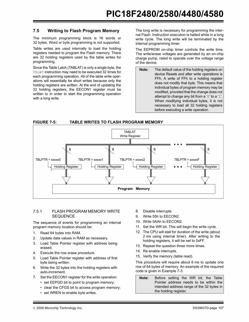
PIC18F2480/2580/4480/4580
7.5 Writing to Flash Program MemoryThe minimum programming block is 16 words or32 bytes. Word or byte programming is not supported.Table writes are used internally to load the holdingregisters needed to program the Flash memory. Thereare 32 holding registers used by the table writes forprogramming.Since the Table Latch (TABLAT) is only a single byte, theTBLWT instruction may need to be executed 32 times foreach programming operation. All of the table write oper-ations will essentially be short writes because only theholding registers are written. At the end of updating the32 holding registers, the EECON1 register must bewritten to in order to start the programming operationwith a long write.The long write is necessary for programming the inter-nal Flash. Instruction execution is halted while in a longwrite cycle. The long write will be terminated by theinternal programming timer. The EEPROM on-chip timer controls the write time.The write/erase voltages are generated by an on-chipcharge pump, rated to operate over the voltage rangeof the device.
FIGURE 7-5: TABLE WRITES TO FLASH PROGRAM MEMORY
7.5.1 FLASH PROGRAM MEMORY WRITE SEQUENCE
The sequence of events for programming an internalprogram memory location should be:1. Read 64 bytes into RAM.2. Update data values in RAM as necessary.3. Load Table Pointer register with address being
erased.4. Execute the row erase procedure.5. Load Table Pointer register with address of first
byte being written.6. Write the 32 bytes into the holding registers with
auto-increment.7. Set the EECON1 register for the write operation:
• set EEPGD bit to point to program memory;• clear the CFGS bit to access program memory;• set WREN to enable byte writes.
8. Disable interrupts.9. Write 55h to EECON2.10. Write 0AAh to EECON2.11. Set the WR bit. This will begin the write cycle.12. The CPU will stall for duration of the write (about
2 ms using internal timer). After writing to theholding registers, it will be set to 0xFF.
13. Repeat the question three more times.14. Re-enable interrupts.15. Verify the memory (table read).This procedure will require about 6 ms to update onerow of 64 bytes of memory. An example of the requiredcode is given in Example 7-3.
Note: The default value of the holding registers ondevice Resets and after write operations isFFh. A write of FFh to a holding registerdoes not modify that byte. This means thatindividual bytes of program memory may bemodified, provided that the change does notattempt to change any bit from a ‘0’ to a ‘1’.When modifying individual bytes, it is notnecessary to load all 32 holding registersbefore executing a write operation.
TBLPTR = xxxxxFTBLPTR = xxxxx1TBLPTR = xxxxx0 TBLPTR = xxxxx2
Program Memory
Holding Register Holding Register Holding Register Holding Register
8 8 8 8
TABLAT Write Register
Note: Before setting the WR bit, the TablePointer address needs to be within theintended address range of the 32 bytes inthe holding register.
© 2009 Microchip Technology Inc. DS39637D-page 107

PIC18F2480/2580/4480/4580
EXAMPLE 7-3: WRITING TO FLASH PROGRAM MEMORYMOVLW D'64 ; number of bytes in erase blockMOVWF COUNTERMOVLW BUFFER_ADDR_HIGH ; point to bufferMOVWF FSR0HMOVLW BUFFER_ADDR_LOWMOVWF FSR0LMOVLW CODE_ADDR_UPPER ; Load TBLPTR with the baseMOVWF TBLPTRU ; address of the memory blockMOVLW CODE_ADDR_HIGHMOVWF TBLPTRHMOVLW CODE_ADDR_LOWMOVWF TBLPTRL
READ_BLOCKTBLRD*+ ; read into TABLAT, and incMOVF TABLAT, W ; get dataMOVWF POSTINC0 ; store dataDECFSZ COUNTER ; done?BRA READ_BLOCK ; repeat
MODIFY_WORDMOVLW DATA_ADDR_HIGH ; point to bufferMOVWF FSR0HMOVLW DATA_ADDR_LOWMOVWF FSR0LMOVLW NEW_DATA_LOW ; update buffer wordMOVWF POSTINC0MOVLW NEW_DATA_HIGHMOVWF INDF0
ERASE_BLOCKMOVLW CODE_ADDR_UPPER ; load TBLPTR with the baseMOVWF TBLPTRU ; address of the memory blockMOVLW CODE_ADDR_HIGHMOVWF TBLPTRH MOVLW CODE_ADDR_LOWMOVWF TBLPTRL BSF EECON1, EEPGD ; point to Flash program memoryBCF EECON1, CFGS ; access Flash program memoryBSF EECON1, WREN ; enable write to memoryBSF EECON1, FREE ; enable Row Erase operationBCF INTCON, GIE ; disable interruptsMOVLW 55h
Required MOVWF EECON2 ; write 55hSequence MOVLW 0AAh
MOVWF EECON2 ; write 0AAhBSF EECON1, WR ; start erase (CPU stall)BSF INTCON, GIE ; re-enable interruptsTBLRD*- ; dummy read decrementMOVLW BUFFER_ADDR_HIGH ; point to bufferMOVWF FSR0HMOVLW BUFFER_ADDR_LOWMOVWF FSR0LMOVLW D’4’MOVWF COUNTER1
WRITE_BUFFER_BACKMOVLW D’64 ; number of bytes in holding registerMOVWF COUNTER
WRITE_BYTE_TO_HREGSMOVF POSTINC0, W ; get low byte of buffer dataMOVWF TABLAT ; present data to table latchTBLWT+* ; write data, perform a short write
; to internal TBLWT holding register.DECFSZ COUNTER ; loop until buffers are fullBRA WRITE_BYTE_TO_HREGS
DS39637D-page 108 © 2009 Microchip Technology Inc.

PIC18F2480/2580/4480/4580
EXAMPLE 7-3: WRITING TO FLASH PROGRAM MEMORY (CONTINUED)7.5.2 WRITE VERIFYDepending on the application, good programmingpractice may dictate that the value written to the mem-ory should be verified against the original value. Thisshould be used in applications where excessive writescan stress bits near the specification limit.
7.5.3 UNEXPECTED TERMINATION OF WRITE OPERATION
If a write is terminated by an unplanned event, such asloss of power or an unexpected Reset, the memorylocation just programmed should be verified and repro-grammed if needed. If the write operation is interruptedby a MCLR Reset or a WDT time-out Reset duringnormal operation, the user can check the WRERR bitand rewrite the location(s) as needed.
7.5.4 PROTECTION AGAINST SPURIOUS WRITES
To protect against spurious writes to Flash programmemory, the write initiate sequence must also befollowed. See Section 25.0 “Special Features of theCPU” for more detail.
7.6 Flash Program Operation During Code Protection
See Section 25.5 “Program Verification and CodeProtection” for details on code protection of Flashprogram memory.
TABLE 7-2: REGISTERS ASSOCIATED WITH PROGRAM FLASH MEMORY
PROGRAM_MEMORYBSF EECON1,EEPGD ; point to Flash program memoryBCF EECON1, CFGS ; access Flash program memoryBSF EECON1, WREN ; enable write to memoryBCF INTCON, GIE ; disable interruptsMOVLW 55h
Required MOVWF EECON2 ; write 55hSequence MOVLW 0AAh
MOVWF EECON2 ; write 0AAhBSF EECON1, WR ; start program (CPU stall)DECFSZ COUNTER1BRA WRITE_BUFFER_BACKBSF INTCON, GIE ; re-enable interruptsBCF EECON1, WREN ; disable write to memory
Name Bit 7 Bit 6 Bit 5 Bit 4 Bit 3 Bit 2 Bit 1 Bit 0Reset Values
on Page:
TBLPTRU — — bit21(3) Program Memory Table Pointer Upper Byte (TBLPTR<20:16>) 55TBPLTRH Program Memory Table Pointer High Byte (TBLPTR<15:8>) 55TBLPTRL Program Memory Table Pointer High Byte (TBLPTR<7:0>) 55TABLAT Program Memory Table Latch 55INTCON GIE/GIEH PEIE/GIEL TMR0IE INTE RBIE TMR0IF INTF RBIF 55EECON2 EEPROM Control Register 2 (not a physical register) 57EECON1 EEPGD CFGS — FREE WRERR WREN WR RD 57IPR2 OSCFIP CMIP(2) — EEIP BCLIP HLVDIP TMR3IP ECCP1IP(1) 57PIR2 OSCFIF CMIF(2) — EEIF BCLIF HLVDIF TMR3IF ECCP1IF(1) 58PIE2 OSCFIE CMIE(2) — EEIE BCLIE HLVDIE TMR3IE ECCP1IE(1) 58Legend: — = unimplemented, read as ‘0’. Shaded cells are not used during Flash/EEPROM access.Note 1: These bits are available in PIC18F4X80 devices only.
2: These bits are available in PIC18F4X80 devices and reserved in PIC18F2X80 devices.3: This bit is available only in Test mode and Serial Programming mode.
© 2009 Microchip Technology Inc. DS39637D-page 109

PIC18F2480/2580/4480/4580
NOTES:DS39637D-page 110 © 2009 Microchip Technology Inc.

PIC18F2480/2580/4480/4580
8.0 DATA EEPROM MEMORY The data EEPROM is a nonvolatile memory array,separate from the data RAM and program memory, thatis used for long-term storage of program data. It is notdirectly mapped in either the register file or programmemory space, but is indirectly addressed through theSpecial Function Registers (SFRs). The EEPROM isreadable and writable during normal operation over theentire VDD range.
Four SFRs are used to read and write to the dataEEPROM, as well as the program memory. They are:
• EECON1• EECON2• EEDATA• EEADR
The data EEPROM allows byte read and write. Wheninterfacing to the data memory block, EEDATA holdsthe 8-bit data for read/write and the EEADR registerholds the address of the EEPROM location beingaccessed.
The EEPROM data memory is rated for high erase/writecycle endurance. A byte write automatically erases thelocation and writes the new data (erase-before-write).The write time is controlled by an on-chip timer; it willvary with voltage and temperature, as well as from chipto chip. Please refer to parameter D122 (Table 28-1 inSection 28.0 “Electrical Characteristics”) for exactlimits.
8.1 EEADR RegisterThe EEADR register is used to address the dataEEPROM for read and write operations. The 8-bitrange of the register can address a memory range of256 bytes (00h to FFh).
8.2 EECON1 and EECON2 RegistersAccess to the data EEPROM is controlled by tworegisters: EECON1 and EECON2. These are the sameregisters which control access to the program memoryand are used in a similar manner for the dataEEPROM.
The EECON1 register (Register 8-1) is the controlregister for data and program memory access. Controlbit, EEPGD, determines if the access will be to programor data EEPROM memory. When clear, operations willaccess the data EEPROM memory. When set, programmemory is accessed.
Control bit, CFGS, determines if the access will be tothe Configuration registers or to program memory/dataEEPROM memory. When set, subsequent operationsaccess Configuration registers. When CFGS is clear,the EEPGD bit selects either program Flash or dataEEPROM memory.
The WREN bit, when set, will allow a write operation.On power-up, the WREN bit is clear. The WRERR bit isset in hardware when the WREN bit is set and clearedwhen the internal programming timer expires and thewrite operation is complete.
The WR control bit initiates write operations. The bitcannot be cleared, only set, in software; it is cleared inhardware at the completion of the write operation.
Control bits, RD and WR, start read and erase/writeoperations, respectively. These bits are set by firmwareand cleared by hardware at the completion of theoperation.
The RD bit cannot be set when accessing programmemory (EEPGD = 1). Program memory is read usingtable read instructions. See Section 7.1 “Table Readsand Table Writes” regarding table reads.
The EECON2 register is not a physical register. It isused exclusively in the memory write and erasesequences. Reading EECON2 will read all ‘0’s.
Note: During normal operation, the WRERR isread as ‘1’. This can indicate that a writeoperation was prematurely terminated bya Reset, or a write operation wasattempted improperly.
Note: The EEIF interrupt flag bit (PIR2<4>) is setwhen the write is complete. It must becleared in software.
© 2009 Microchip Technology Inc. DS39637D-page 111

PIC18F2480/2580/4480/4580
REGISTER 8-1: EECON1: DATA EEPROM CONTROL REGISTER 1R/W-x R/W-x U-0 R/W-0 R/W-x R/W-0 R/S-0 R/S-0EEPGD CFGS — FREE WRERR(1) WREN WR RD
bit 7 bit 0
Legend: S = Settable bitR = Readable bit W = Writable bit U = Unimplemented bit, read as ‘0’-n = Value at POR ‘1’ = Bit is set ‘0’ = Bit is cleared x = Bit is unknown
bit 7 EEPGD: Flash Program or Data EEPROM Memory Select bit1 = Access Flash program memory0 = Access data EEPROM memory
bit 6 CFGS: Flash Program/Data EEPROM or Configuration Select bit1 = Access Configuration registers0 = Access Flash program or data EEPROM memory
bit 5 Unimplemented: Read as ‘0’bit 4 FREE: Flash Row Erase Enable bit
1 = Erase the program memory row addressed by TBLPTR on the next WR command (cleared bycompletion of erase operation)
0 = Perform write onlybit 3 WRERR: Flash Program/Data EEPROM Error Flag bit(1)
1 = A write operation is prematurely terminated (any Reset during self-timed programming in normaloperation or an improper write attempt)
0 = The write operation completedbit 2 WREN: Flash Program/Data EEPROM Write Enable bit
1 = Allows write cycles to Flash program/data EEPROM0 = Inhibits write cycles to Flash program/data EEPROM
bit 1 WR: Write Control bit1 = Initiates a data EEPROM erase/write cycle or a program memory erase cycle or write cycle
(The operation is self-timed and the bit is cleared by hardware once write is complete. The WR bit can only be set (not cleared) in software.)
0 = Write cycle to the EEPROM is completebit 0 RD: Read Control bit
1 = Initiates an EEPROM read (Read takes one cycle. RD is cleared in hardware. The RD bit can onlybe set (not cleared) in software. RD bit cannot be set when EEPGD = 1 or CFGS = 1.)
0 = Does not initiate an EEPROM read
Note 1: When a WRERR occurs, the EEPGD and CFGS bits are not cleared. This allows tracing of the error condition.
DS39637D-page 112 © 2009 Microchip Technology Inc.

PIC18F2480/2580/4480/4580
8.3 Reading the Data EEPROMMemoryTo read a data memory location, the user must write theaddress to the EEADR register, clear the EEPGDcontrol bit (EECON1<7>) and then set control bit, RD(EECON1<0>). The data is available on the very nextinstruction cycle; therefore, the EEDATA register canbe read by the next instruction. EEDATA will hold thisvalue until another read operation, or until it is written toby the user (during a write operation).
The basic process is shown in Example 8-1.
8.4 Writing to the Data EEPROM Memory
To write an EEPROM data location, the address mustfirst be written to the EEADR register and the datawritten to the EEDATA register. The sequence inExample 8-2 must be followed to initiate the write cycle.
The write will not begin if this sequence is not exactlyfollowed (write 55h to EECON2, write 0AAh toEECON2, then set WR bit) for each byte. It is stronglyrecommended that interrupts be disabled during thiscode segment.
Additionally, the WREN bit in EECON1 must be set toenable writes. This mechanism prevents accidentalwrites to data EEPROM due to unexpected code exe-cution (i.e., runaway programs). The WREN bit shouldbe kept clear at all times, except when updating theEEPROM. The WREN bit is not cleared by hardware.
After a write sequence has been initiated, EECON1,EEADR and EEDATA cannot be modified. The WR bitwill be inhibited from being set unless the WREN bit isset. The WREN bit must be set on a previous instruc-tion. Both WR and WREN cannot be set with the sameinstruction.
At the completion of the write cycle, the WR bit iscleared in hardware and the EEPROM Interrupt Flag bit(EEIF) is set. The user may either enable this interrupt,or poll this bit. EEIF must be cleared by software.
8.5 Write VerifyDepending on the application, good programmingpractice may dictate that the value written to the mem-ory should be verified against the original value. Thisshould be used in applications where excessive writescan stress bits near the specification limit.
EXAMPLE 8-1: DATA EEPROM READ
EXAMPLE 8-2: DATA EEPROM WRITE
MOVLW DATA_EE_ADDR ;MOVWF EEADR ; Data Memory Address to readBCF EECON1, EEPGD ; Point to DATA memoryBCF EECON1, CFGS ; Access EEPROMBSF EECON1, RD ; EEPROM ReadMOVF EEDATA, W ; W = EEDATA
MOVLW DATA_EE_ADDR ;MOVWF EEADR ; Data Memory Address to writeMOVLW DATA_EE_DATA ;MOVWF EEDATA ; Data Memory Value to writeBCF EECON1, EEPGD ; Point to DATA memoryBCF EECON1, CFGS ; Access EEPROMBSF EECON1, WREN ; Enable writes
BCF INTCON, GIE ; Disable InterruptsMOVLW 55h ;
Required MOVWF EECON2 ; Write 55hSequence MOVLW 0AAh ;
MOVWF EECON2 ; Write 0AAhBSF EECON1, WR ; Set WR bit to begin writeBTFSC EECON1, WR ; Wait for write to completeBRA $-2BSF INTCON, GIE ; Enable Interrupts
; User code executionBCF EECON1, WREN ; Disable writes on write complete (EEIF set)
© 2009 Microchip Technology Inc. DS39637D-page 113
PIC18F2480/2580/4480/4580
8.6 Operation During Code-ProtectData EEPROM memory has its own code-protect bits inConfiguration Words. External read and writeoperations are disabled if code protection is enabled.The microcontroller itself can both read and write to theinternal data EEPROM, regardless of the state of thecode-protect Configuration bit. Refer to Section 25.0“Special Features of the CPU” for additionalinformation.
8.7 Protection Against Spurious WriteThere are conditions when the device may not want towrite to the data EEPROM memory. To protect againstspurious EEPROM writes, various mechanisms havebeen implemented. On power-up, the WREN bit iscleared. In addition, writes to the EEPROM are blockedduring the Power-up Timer period (TPWRT,parameter 33).
The write initiate sequence and the WREN bit togetherhelp prevent an accidental write during brown-out,power glitch or software malfunction.
8.8 Using the Data EEPROMThe data EEPROM is a high-endurance, byte address-able array that has been optimized for the storage offrequently changing information (e.g., programvariables or other data that are updated often).Frequently changing values will typically be updatedmore often than specification D124. If this is not thecase, an array refresh must be performed. For thisreason, variables that change infrequently (such asconstants, IDs, calibration, etc.) should be stored inFlash program memory.
A simple data EEPROM refresh routine is shown inExample 8-3.
EXAMPLE 8-3: DATA EEPROM REFRESH ROUTINE
Note: If data EEPROM is only used to storeconstants and/or data that changes rarely,an array refresh is likely not required. Seespecification D124.
CLRF EEADR ; Start at address 0BCF EECON1, CFGS ; Set for memoryBCF EECON1, EEPGD ; Set for Data EEPROMBCF INTCON, GIE ; Disable interruptsBSF EECON1, WREN ; Enable writes
LOOP ; Loop to refresh arrayBSF EECON1, RD ; Read current addressMOVLW 55h ;MOVWF EECON2 ; Write 55hMOVLW 0AAh ;MOVWF EECON2 ; Write 0AAhBSF EECON1, WR ; Set WR bit to begin writeBTFSC EECON1, WR ; Wait for write to completeBRA $-2INCFSZ EEADR, F ; Increment addressBRA LOOP ; Not zero, do it again
BCF EECON1, WREN ; Disable writesBSF INTCON, GIE ; Enable interrupts
DS39637D-page 114 © 2009 Microchip Technology Inc.

PIC18F2480/2580/4480/4580
TABLE 8-1: REGISTERS ASSOCIATED WITH DATA EEPROM MEMORYName Bit 7 Bit 6 Bit 5 Bit 4 Bit 3 Bit 2 Bit 1 Bit 0Reset Values
on Page:
INTCON GIE/GIEH PEIE/GIEL TMR0IE INT0IE RBIE TMR0IF INT0IF RBIF 55EEADR EEPROM Address Register 57EEDATA EEPROM Data Register 57EECON2 EEPROM Control Register 2 (not a physical register) 57EECON1 EEPGD CFGS — FREE WRERR WREN WR RD 57IPR2 OSCFIP CMIP(1) — EEIP BCLIP HLVDIP TMR3IP ECCP1IP(1) 57PIR2 OSCFIF CMIF(1) — EEIF BCLIF HLVDIF TMR3IF ECCP1IF(1) 58PIE2 OSCFIE CMIE(1) — EEIE BCLIE HLVDIE TMR3IE ECCP1IE(1) 58Legend: — = unimplemented, read as ‘0’. Shaded cells are not used during Flash/EEPROM access.Note 1: These bits are available in PIC18F4X80 devices and reserved in PIC18F2X80 devices.
© 2009 Microchip Technology Inc. DS39637D-page 115

PIC18F2480/2580/4480/4580
NOTES:DS39637D-page 116 © 2009 Microchip Technology Inc.

PIC18F2480/2580/4480/4580
9.0 8 x 8 HARDWARE MULTIPLIER
9.1 IntroductionAll PIC18 devices include an 8 x 8 hardware multiplieras part of the ALU. The multiplier performs an unsignedoperation and yields a 16-bit result that is stored in theproduct register pair, PRODH:PRODL. The multiplier’soperation does not affect any flags in the STATUSregister.
Making multiplication a hardware operation allows it tobe completed in a single instruction cycle. This has theadvantages of higher computational throughput andreduced code size for multiplication algorithms andallows the PIC18 devices to be used in many applica-tions previously reserved for digital signal processors.A comparison of various hardware and softwaremultiply operations, along with the savings in memoryand execution time, is shown in Table 9-1.
9.2 OperationExample 9-1 shows the instruction sequence for an8 x 8 unsigned multiplication. Only one instruction isrequired when one of the arguments is already loadedin the WREG register.
Example 9-2 shows the sequence to do an 8 x 8 signedmultiplication. To account for the signed bits of thearguments, each argument’s Most Significant bit (MSb)is tested and the appropriate subtractions are done.
EXAMPLE 9-1: 8 x 8 UNSIGNED MULTIPLY ROUTINE
EXAMPLE 9-2: 8 x 8 SIGNED MULTIPLY ROUTINE
TABLE 9-1: PERFORMANCE COMPARISON FOR VARIOUS MULTIPLY OPERATIONS
MOVF ARG1, W ; MULWF ARG2 ; ARG1 * ARG2 ->
; PRODH:PRODL
MOVF ARG1, W MULWF ARG2 ; ARG1 * ARG2 ->
; PRODH:PRODL BTFSC ARG2, SB ; Test Sign Bit SUBWF PRODH, F ; PRODH = PRODH
; - ARG1 MOVF ARG2, WBTFSC ARG1, SB ; Test Sign Bit SUBWF PRODH, F ; PRODH = PRODH
; - ARG2
Routine Multiply MethodProgramMemory(Words)
Cycles(Max)
Time
@ 40 MHz @ 10 MHz @ 4 MHz
8 x 8 unsignedWithout hardware multiply 13 69 6.9 μs 27.6 μs 69 μs
Hardware multiply 1 1 100 ns 400 ns 1 μs
8 x 8 signedWithout hardware multiply 33 91 9.1 μs 36.4 μs 91 μs
Hardware multiply 6 6 600 ns 2.4 μs 6 μs
16 x 16 unsignedWithout hardware multiply 21 242 24.2 μs 96.8 μs 242 μs
Hardware multiply 28 28 2.8 μs 11.2 μs 28 μs
16 x 16 signedWithout hardware multiply 52 254 25.4 μs 102.6 μs 254 μs
Hardware multiply 35 40 4.0 μs 16.0 μs 40 μs
© 2009 Microchip Technology Inc. DS39637D-page 117

PIC18F2480/2580/4480/4580
Example 9-3 shows the sequence to do a 16 x 16unsigned multiplication. Equation 9-1 shows thealgorithm that is used. The 32-bit result is stored in fourregisters (RES3:RES0).EQUATION 9-1: 16 x 16 UNSIGNED MULTIPLICATION ALGORITHM
EXAMPLE 9-3: 16 x 16 UNSIGNED MULTIPLY ROUTINE
Example 9-4 shows the sequence to do a 16 x 16signed multiply. Equation 9-2 shows the algorithmused. The 32-bit result is stored in four registers(RES3:RES0). To account for the signed bits of thearguments, the MSb for each argument pair is testedand the appropriate subtractions are done.
EQUATION 9-2: 16 x 16 SIGNED MULTIPLICATION ALGORITHM
EXAMPLE 9-4: 16 x 16 SIGNED MULTIPLY ROUTINE
RES3:RES0 = ARG1H:ARG1L • ARG2H:ARG2L= (ARG1H • ARG2H • 216) +
(ARG1H • ARG2L • 28) +(ARG1L • ARG2H • 28) +(ARG1L • ARG2L)
MOVF ARG1L, W MULWF ARG2L ; ARG1L * ARG2L->
; PRODH:PRODL MOVFF PRODH, RES1 ; MOVFF PRODL, RES0 ;
; MOVF ARG1H, W MULWF ARG2H ; ARG1H * ARG2H->
; PRODH:PRODL MOVFF PRODH, RES3 ; MOVFF PRODL, RES2 ;
; MOVF ARG1L, W MULWF ARG2H ; ARG1L * ARG2H->
; PRODH:PRODL MOVF PRODL, W ;ADDWF RES1, F ; Add cross MOVF PRODH, W ; products ADDWFC RES2, F ; CLRF WREG ; ADDWFC RES3, F ;
; MOVF ARG1H, W ; MULWF ARG2L ; ARG1H * ARG2L->
; PRODH:PRODL MOVF PRODL, W ; ADDWF RES1, F ; Add cross MOVF PRODH, W ; products ADDWFC RES2, F ; CLRF WREG ; ADDWFC RES3, F ;
RES3:RES0 = ARG1H:ARG1L • ARG2H:ARG2L= (ARG1H • ARG2H • 216) +
(ARG1H • ARG2L • 28) +(ARG1L • ARG2H • 28) +(ARG1L • ARG2L) +(-1 • ARG2H<7> • ARG1H:ARG1L • 216) +(-1 • ARG1H<7> • ARG2H:ARG2L • 216)
MOVF ARG1L, W MULWF ARG2L ; ARG1L * ARG2L ->
; PRODH:PRODL MOVFF PRODH, RES1 ; MOVFF PRODL, RES0 ;
; MOVF ARG1H, W MULWF ARG2H ; ARG1H * ARG2H ->
; PRODH:PRODL MOVFF PRODH, RES3 ; MOVFF PRODL, RES2 ;
; MOVF ARG1L,W MULWF ARG2H ; ARG1L * ARG2H ->
; PRODH:PRODL MOVF PRODL, W ; ADDWF RES1, F ; Add cross MOVF PRODH, W ; products ADDWFC RES2, F ; CLRF WREG ; ADDWFC RES3, F ;
; MOVF ARG1H, W ; MULWF ARG2L ; ARG1H * ARG2L ->
; PRODH:PRODL MOVF PRODL, W ; ADDWF RES1, F ; Add cross MOVF PRODH, W ; products ADDWFC RES2, F ; CLRF WREG ; ADDWFC RES3, F ;
; BTFSS ARG2H, 7 ; ARG2H:ARG2L neg? BRA SIGN_ARG1 ; no, check ARG1 MOVF ARG1L, W ; SUBWF RES2 ; MOVF ARG1H, W ; SUBWFB RES3
; SIGN_ARG1
BTFSS ARG1H, 7 ; ARG1H:ARG1L neg? BRA CONT_CODE ; no, done MOVF ARG2L, W ; SUBWF RES2 ; MOVF ARG2H, W ; SUBWFB RES3
; CONT_CODE :
DS39637D-page 118 © 2009 Microchip Technology Inc.

PIC18F2480/2580/4480/4580
10.0 INTERRUPTSThe PIC18F2480/2580/4480/4580 devices havemultiple interrupt sources and an interrupt priorityfeature that allows each interrupt source to be assigneda high-priority level or a low-priority level. The high-priority interrupt vector is at 000008h and the low-priority interrupt vector is at 000018h. High-priorityinterrupt events will interrupt any low-priority interruptsthat may be in progress.
There are ten registers which are used to controlinterrupt operation. These registers are:
• RCON• INTCON• INTCON2• INTCON3• PIR1, PIR2, PIR3• PIE1, PIE2, PIE3• IPR1, IPR2, IPR3
It is recommended that the Microchip header filessupplied with MPLAB® IDE be used for the symbolic bitnames in these registers. This allows the assembler/compiler to automatically take care of the placement ofthese bits within the specified register.
Each interrupt source has three bits to control itsoperation. The functions of these bits are:
• Flag bit to indicate that an interrupt event occurred
• Enable bit that allows program execution to branch to the interrupt vector address when the flag bit is set
• Priority bit to select high priority or low priority
The interrupt priority feature is enabled by setting theIPEN bit (RCON<7>). When interrupt priority is enabled,there are two bits which enable interrupts globally. Set-ting the GIEH bit (INTCON<7>) enables all interruptsthat have the priority bit set (high priority). Setting theGIEL bit (INTCON<6>) enables all interrupts that havethe priority bit cleared (low priority). When the interruptflag, enable bit and appropriate global interrupt enablebit are set, the interrupt will vector immediately toaddress 000008h or 000018h, depending on the prioritybit setting. Individual interrupts can be disabled throughtheir corresponding enable bits.
When the IPEN bit is cleared (default state), theinterrupt priority feature is disabled and interrupts arecompatible with PIC® mid-range devices. In Compati-bility mode, the interrupt priority bits for each sourcehave no effect. INTCON<6> is the PEIE bit, whichenables/disables all peripheral interrupt sources. INT-CON<7> is the GIE bit, which enables/disables allinterrupt sources. All interrupts branch to address000008h in Compatibility mode.
When an interrupt is responded to, the global interruptenable bit is cleared to disable further interrupts. If theIPEN bit is cleared, this is the GIE bit. If interrupt prioritylevels are used, this will be either the GIEH or GIEL bit.High-priority interrupt sources can interrupt a low-priority interrupt. Low-priority interrupts are notprocessed while high-priority interrupts are in progress.
The return address is pushed onto the stack and thePC is loaded with the interrupt vector address(000008h or 000018h). Once in the Interrupt ServiceRoutine, the source(s) of the interrupt can be deter-mined by polling the interrupt flag bits. The interruptflag bits must be cleared in software before re-enablinginterrupts to avoid recursive interrupts.
The “return from interrupt” instruction, RETFIE, exitsthe interrupt routine and sets the GIE bit (GIEH or GIELif priority levels are used), which re-enables interrupts.
For external interrupt events, such as the INTx pins orthe PORTB input change interrupt, the interrupt latencywill be three to four instruction cycles. The exactlatency is the same for one or two-cycle instructions.Individual interrupt flag bits are set, regardless of thestatus of their corresponding enable bit or the GIE bit.
Note: Do not use the MOVFF instruction to modifyany of the Interrupt Control registers whileany interrupt is enabled. Doing so maycause erratic microcontroller behavior.
© 2009 Microchip Technology Inc. DS39637D-page 119

PIC18F2480/2580/4480/4580
FIGURE 10-1: INTERRUPT LOGICTMR0IE
GIEH/GIE
GIEL/PEIE
Wake-up if in Sleep Mode
Interrupt to CPUVector to Location0008h
INT2IFINT2IEINT2IP
INT1IFINT1IEINT1IP
TMR0IFTMR0IETMR0IP
RBIFRBIERBIP
IPEN
TMR0IF
TMR0IP
INT1IFINT1IEINT1IPINT2IFINT2IEINT2IP
RBIFRBIERBIP
INT0IFINT0IE
GIEL/PEIE
Interrupt to CPUVector to Location
IPEN
IPE
0018h
Peripheral Interrupt Flag bitPeripheral Interrupt Enable bitPeripheral Interrupt Priority bit
Peripheral Interrupt Flag bitPeripheral Interrupt Enable bitPeripheral Interrupt Priority bit
TMR1IFTMR1IETMR1IP
XXXXIFXXXXIEXXXXIP
Additional Peripheral Interrupts
TMR1IFTMR1IETMR1IP
High-Priority Interrupt Generation
Low-Priority Interrupt Generation
XXXXIFXXXXIEXXXXIP
Additional Peripheral Interrupts
GIE/GEIH
DS39637D-page 120 © 2009 Microchip Technology Inc.

PIC18F2480/2580/4480/4580
10.1 INTCON RegistersThe INTCON registers are readable and writableregisters, which contain various enable, priority andflag bits.Note: Interrupt flag bits are set when an interruptcondition occurs regardless of the state ofits corresponding enable bit or the globalinterrupt enable bit. User software shouldensure the appropriate interrupt flag bitsare clear prior to enabling an interrupt.This feature allows for software polling.
REGISTER 10-1: INTCON: INTERRUPT CONTROL REGISTER
R/W-0 R/W-0 R/W-0 R/W-0 R/W-0 R/W-0 R/W-0 R/W-xGIE/GIEH PEIE/GIEL TMR0IE INT0IE RBIE TMR0IF INT0IF RBIF(1)
bit 7 bit 0
Legend:R = Readable bit W = Writable bit U = Unimplemented bit, read as ‘0’-n = Value at POR ‘1’ = Bit is set ‘0’ = Bit is cleared x = Bit is unknown
bit 7 GIE/GIEH: Global Interrupt Enable bitWhen IPEN = 0:1 = Enables all unmasked interrupts0 = Disables all interrupts When IPEN = 1:1 = Enables all high-priority interrupts 0 = Disables all high-priority interrupts
bit 6 PEIE/GIEL: Peripheral Interrupt Enable bitWhen IPEN = 0:1 = Enables all unmasked peripheral interrupts 0 = Disables all peripheral interrupts When IPEN = 1:1 = Enables all low-priority peripheral interrupts 0 = Disables all low-priority peripheral interrupts
bit 5 TMR0IE: TMR0 Overflow Interrupt Enable bit 1 = Enables the TMR0 overflow interrupt 0 = Disables the TMR0 overflow interrupt
bit 4 INT0IE: INT0 External Interrupt Enable bit 1 = Enables the INT0 external interrupt 0 = Disables the INT0 external interrupt
bit 3 RBIE: RB Port Change Interrupt Enable bit 1 = Enables the RB port change interrupt 0 = Disables the RB port change interrupt
bit 2 TMR0IF: TMR0 Overflow Interrupt Flag bit 1 = TMR0 register has overflowed (must be cleared in software) 0 = TMR0 register did not overflow
bit 1 INT0IF: INT0 External Interrupt Flag bit 1 = The INT0 external interrupt occurred (must be cleared in software) 0 = The INT0 external interrupt did not occur
bit 0 RBIF: RB Port Change Interrupt Flag bit(1) 1 = At least one of the RB<7:4> pins changed state (must be cleared in software)0 = None of the RB<7:4> pins have changed state
Note 1: A mismatch condition will continue to set this bit. Reading PORTB will end the mismatch condition and allow the bit to be cleared.
© 2009 Microchip Technology Inc. DS39637D-page 121

PIC18F2480/2580/4480/4580
REGISTER 10-2: INTCON2: INTERRUPT CONTROL REGISTER 2
R/W-1 R/W-1 R/W-1 R/W-1 U-0 R/W-1 U-0 R/W-1
RBPU INTEDG0 INTEDG1 INTEDG2 — TMR0IP — RBIPbit 7 bit 0
Legend:R = Readable bit W = Writable bit U = Unimplemented bit, read as ‘0’-n = Value at POR ‘1’ = Bit is set ‘0’ = Bit is cleared x = Bit is unknown
bit 7 RBPU: PORTB Pull-up Enable bit 1 = All PORTB pull-ups are disabled 0 = PORTB pull-ups are enabled by individual port latch values
bit 6 INTEDG0: External Interrupt 0 Edge Select bit 1 = Interrupt on rising edge 0 = Interrupt on falling edge
bit 5 INTEDG1: External Interrupt 1 Edge Select bit 1 = Interrupt on rising edge 0 = Interrupt on falling edge
bit 4 INTEDG2: External Interrupt 2 Edge Select bit 1 = Interrupt on rising edge 0 = Interrupt on falling edge
bit 3 Unimplemented: Read as ‘0’bit 2 TMR0IP: TMR0 Overflow Interrupt Priority bit
1 = High priority 0 = Low priority
bit 1 Unimplemented: Read as ‘0’bit 0 RBIP: RB Port Change Interrupt Priority bit
1 = High priority 0 = Low priority
Note: Interrupt flag bits are set when an interrupt condition occurs regardless of the state of its correspondingenable bit or the global interrupt enable bit. User software should ensure the appropriate interrupt flag bitsare clear prior to enabling an interrupt. This feature allows for software polling.
DS39637D-page 122 © 2009 Microchip Technology Inc.

PIC18F2480/2580/4480/4580
REGISTER 10-3: INTCON3: INTERRUPT CONTROL REGISTER 3
R/W-1 R/W-1 U-0 R/W-0 R/W-0 U-0 R/W-0 R/W-0INT2IP INT1IP — INT2IE INT1IE — INT2IF INT1IF
bit 7 bit 0
Legend:R = Readable bit W = Writable bit U = Unimplemented bit, read as ‘0’-n = Value at POR ‘1’ = Bit is set ‘0’ = Bit is cleared x = Bit is unknown
bit 7 INT2IP: INT2 External Interrupt Priority bit1 = High priority 0 = Low priority
bit 6 INT1IP: INT1 External Interrupt Priority bit1 = High priority 0 = Low priority
bit 5 Unimplemented: Read as ‘0’bit 4 INT2IE: INT2 External Interrupt Enable bit
1 = Enables the INT2 external interrupt 0 = Disables the INT2 external interrupt
bit 3 INT1IE: INT1 External Interrupt Enable bit 1 = Enables the INT1 external interrupt 0 = Disables the INT1 external interrupt
bit 2 Unimplemented: Read as ‘0’ bit 1 INT2IF: INT2 External Interrupt Flag bit
1 = The INT2 external interrupt occurred (must be cleared in software) 0 = The INT2 external interrupt did not occur
bit 0 INT1IF: INT1 External Interrupt Flag bit 1 = The INT1 external interrupt occurred (must be cleared in software) 0 = The INT1 external interrupt did not occur
Note: Interrupt flag bits are set when an interrupt condition occurs regardless of the state of its correspondingenable bit or the global interrupt enable bit. User software should ensure the appropriate interrupt flag bitsare clear prior to enabling an interrupt. This feature allows for software polling.
© 2009 Microchip Technology Inc. DS39637D-page 123

PIC18F2480/2580/4480/4580
10.2 PIR RegistersThe PIR registers contain the individual flag bits for theperipheral interrupts. Due to the number of peripheralinterrupt sources, there are two Peripheral InterruptRequest (Flag) registers (PIR1, PIR2).Note 1: Interrupt flag bits are set when an interruptcondition occurs regardless of the state ofits corresponding enable bit or the globalinterrupt enable bit, GIE (INTCON<7>).
2: User software should ensure the appropri-ate interrupt flag bits are cleared prior toenabling an interrupt and after servicingthat interrupt.
REGISTER 10-4: PIR1: PERIPHERAL INTERRUPT REQUEST (FLAG) REGISTER 1
R/W-0 R/W-0 R-0 R-0 R/W-0 R/W-0 R/W-0 R/W-0PSPIF(1) ADIF RCIF TXIF SSPIF CCP1IF TMR2IF TMR1IF
bit 7 bit 0
Legend:R = Readable bit W = Writable bit U = Unimplemented bit, read as ‘0’-n = Value at POR ‘1’ = Bit is set ‘0’ = Bit is cleared x = Bit is unknown
bit 7 PSPIF: Parallel Slave Port Read/Write Interrupt Flag bit(1)
1 = A read or a write operation has taken place (must be cleared in software) 0 = No read or write has occurred
bit 6 ADIF: A/D Converter Interrupt Flag bit 1 = An A/D conversion completed (must be cleared in software) 0 = The A/D conversion is not complete
bit 5 RCIF: EUSART Receive Interrupt Flag bit 1 = The EUSART receive buffer, RCREG, is full (cleared when RCREG is read) 0 = The EUSART receive buffer is empty
bit 4 TXIF: EUSART Transmit Interrupt Flag bit 1 = The EUSART transmit buffer, TXREG, is empty (cleared when TXREG is written) 0 = The EUSART transmit buffer is full
bit 3 SSPIF: Master Synchronous Serial Port Interrupt Flag bit 1 = The transmission/reception is complete (must be cleared in software)0 = Waiting to transmit/receive
bit 2 CCP1IF: CCP1 Interrupt Flag bit Capture mode: 1 = A TMR1 register capture occurred (must be cleared in software) 0 = No TMR1 register capture occurred Compare mode: 1 = A TMR1 register compare match occurred (must be cleared in software) 0 = No TMR1 register compare match occurredPWM mode: Unused in this mode.
bit 1 TMR2IF: TMR2 to PR2 Match Interrupt Flag bit1 = TMR2 to PR2 match occurred (must be cleared in software) 0 = No TMR2 to PR2 match occurred
bit 0 TMR1IF: TMR1 Overflow Interrupt Flag bit 1 = TMR1 register overflowed (must be cleared in software)0 = TMR1 register did not overflow
Note 1: This bit is reserved on PIC18F2X80 devices; always maintain this bit clear.
DS39637D-page 124 © 2009 Microchip Technology Inc.

PIC18F2480/2580/4480/4580
REGISTER 10-5: PIR2: PERIPHERAL INTERRUPT REQUEST (FLAG) REGISTER 2
R/W-0 R/W-0 U-0 R/W-0 R/W-0 R/W-0 R/W-0 R/W-0OSCFIF CMIF(1) — EEIF BCLIF HLVDIF TMR3IF ECCP1IF(1)
bit 7 bit 0
Legend:R = Readable bit W = Writable bit U = Unimplemented bit, read as ‘0’-n = Value at POR ‘1’ = Bit is set ‘0’ = Bit is cleared x = Bit is unknown
bit 7 OSCFIF: Oscillator Fail Interrupt Flag bit1 = System oscillator failed, clock input has changed to INTOSC (must be cleared in software)0 = System clock operating
bit 6 CMIF: Comparator Interrupt Flag bit(1)
1 = Comparator input has changed (must be cleared in software)0 = Comparator input has not changed
bit 5 Unimplemented: Read as ‘0’bit 4 EEIF: Data EEPROM/Flash Write Operation Interrupt Flag bit
1 = The write operation is complete (must be cleared in software)0 = The write operation is not complete, or has not been started
bit 3 BCLIF: Bus Collision Interrupt Flag bit 1 = A bus collision occurred (must be cleared in software)0 = No bus collision occurred
bit 2 HLVDIF: High/Low-Voltage Detect Interrupt Flag bit 1 = A low-voltage condition occurred (must be cleared in software)0 = The device voltage is above the High/Low-Voltage Detect trip point
bit 1 TMR3IF: TMR3 Overflow Interrupt Flag bit1 = TMR3 register overflowed (must be cleared in software)0 = TMR3 register did not overflow
bit 0 ECCP1IF: CCPx Interrupt Flag bit(1) Capture mode: 1 = A TMR1 register capture occurred (must be cleared in software) 0 = No TMR1 register capture occurred Compare mode: 1 = A TMR1 register compare match occurred (must be cleared in software) 0 = No TMR1 register compare match occurredPWM mode:Unused in this mode.
Note 1: These bits are available in PIC18F4X80 and reserved in PIC18F2X80 devices.
© 2009 Microchip Technology Inc. DS39637D-page 125

PIC18F2480/2580/4480/4580
REGISTER 10-6: PIR3: PERIPHERAL INTERRUPT REQUEST (FLAG) REGISTER 3Mode 0R/W-0 R/W-0 R/W-0 R/W-0 R/W-0 R/W-0 R/W-0 R/W-0IRXIF WAKIF ERRIF TXB2IF TXB1IF(1) TXB0IF(1) RXB1IF RXB0IF
Mode 1,2R/W-0 R/W-0 R/W-0 R/W-0 R/W-0 R/W-0 R/W-0 R/W-0IRXIF WAKIF ERRIF TXBnIF TXB1IF(1) TXB0IF(1) RXBnIF FIFOWMIF(1)
bit 7 bit 0
Legend:R = Readable bit W = Writable bit U = Unimplemented bit, read as ‘0’-n = Value at POR ‘1’ = Bit is set ‘0’ = Bit is cleared x = Bit is unknown
bit 7 IRXIF: CAN Invalid Received Message Interrupt Flag bit1 = An invalid message has occurred on the CAN bus 0 = No invalid message on CAN bus
bit 6 WAKIF: CAN bus Activity Wake-up Interrupt Flag bit1 = Activity on CAN bus has occurred 0 = No activity on CAN bus
bit 5 ERRIF: CAN bus Error Interrupt Flag bit1 = An error has occurred in the CAN module (multiple sources) 0 = No CAN module errors
bit 4 When CAN is in Mode 0:TXB2IF: CAN Transmit Buffer 2 Interrupt Flag bit1 = Transmit Buffer 2 has completed transmission of a message and may be reloaded 0 = Transmit Buffer 2 has not completed transmission of a messageWhen CAN is in Mode 1 or 2:TXBnIF: Any Transmit Buffer Interrupt Flag bit1 = One or more transmit buffers have completed transmission of a message and may be reloaded 0 = No transmit buffer is ready for reload
bit 3 TXB1IF: CAN Transmit Buffer 1 Interrupt Flag bit(1)
1 = Transmit Buffer 1 has completed transmission of a message and may be reloaded 0 = Transmit Buffer 1 has not completed transmission of a message
bit 2 TXB0IF: CAN Transmit Buffer 0 Interrupt Flag bit(1)
1 = Transmit Buffer 0 has completed transmission of a message and may be reloaded 0 = Transmit Buffer 0 has not completed transmission of a message
bit 1 When CAN is in Mode 0:RXB1IF: CAN Receive Buffer 1 Interrupt Flag bit1 = Receive Buffer 1 has received a new message 0 = Receive Buffer 1 has not received a new message When CAN is in Mode 1 or 2:RXBnIF: Any Receive Buffer Interrupt Flag bit1 = One or more receive buffers has received a new message 0 = No receive buffer has received a new message
bit 0 When CAN is in Mode 0:RXB0IF: CAN Receive Buffer 0 Interrupt Flag bit1 = Receive Buffer 0 has received a new message 0 = Receive Buffer 0 has not received a new messageWhen CAN is in Mode 1:Unimplemented: Read as ‘0’When CAN is in Mode 2:FIFOWMIF: FIFO Watermark Interrupt Flag bit(1)
1 = FIFO high watermark is reached 0 = FIFO high watermark is not reached
Note 1: In CAN Mode 1 and 2, these bits are forced to ‘0’.
DS39637D-page 126 © 2009 Microchip Technology Inc.
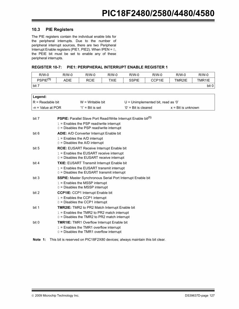
PIC18F2480/2580/4480/4580
10.3 PIE RegistersThe PIE registers contain the individual enable bits forthe peripheral interrupts. Due to the number ofperipheral interrupt sources, there are two PeripheralInterrupt Enable registers (PIE1, PIE2). When IPEN = 0,the PEIE bit must be set to enable any of theseperipheral interrupts.REGISTER 10-7: PIE1: PERIPHERAL INTERRUPT ENABLE REGISTER 1
R/W-0 R/W-0 R/W-0 R/W-0 R/W-0 R/W-0 R/W-0 R/W-0PSPIE(1) ADIE RCIE TXIE SSPIE CCP1IE TMR2IE TMR1IE
bit 7 bit 0
Legend:R = Readable bit W = Writable bit U = Unimplemented bit, read as ‘0’-n = Value at POR ‘1’ = Bit is set ‘0’ = Bit is cleared x = Bit is unknown
bit 7 PSPIE: Parallel Slave Port Read/Write Interrupt Enable bit(1) 1 = Enables the PSP read/write interrupt 0 = Disables the PSP read/write interrupt
bit 6 ADIE: A/D Converter Interrupt Enable bit 1 = Enables the A/D interrupt 0 = Disables the A/D interrupt
bit 5 RCIE: EUSART Receive Interrupt Enable bit1 = Enables the EUSART receive interrupt 0 = Disables the EUSART receive interrupt
bit 4 TXIE: EUSART Transmit Interrupt Enable bit 1 = Enables the EUSART transmit interrupt 0 = Disables the EUSART transmit interrupt
bit 3 SSPIE: Master Synchronous Serial Port Interrupt Enable bit1 = Enables the MSSP interrupt 0 = Disables the MSSP interrupt
bit 2 CCP1IE: CCP1 Interrupt Enable bit 1 = Enables the CCP1 interrupt 0 = Disables the CCP1 interrupt
bit 1 TMR2IE: TMR2 to PR2 Match Interrupt Enable bit1 = Enables the TMR2 to PR2 match interrupt 0 = Disables the TMR2 to PR2 match interrupt
bit 0 TMR1IE: TMR1 Overflow Interrupt Enable bit1 = Enables the TMR1 overflow interrupt 0 = Disables the TMR1 overflow interrupt
Note 1: This bit is reserved on PIC18F2X80 devices; always maintain this bit clear.
© 2009 Microchip Technology Inc. DS39637D-page 127

PIC18F2480/2580/4480/4580
REGISTER 10-8: PIE2: PERIPHERAL INTERRUPT ENABLE REGISTER 2
R/W-0 R/W-0 U-0 R/W-0 R/W-0 R/W-0 R/W-0 R/W-0OSCFIE CMIE(1) — EEIE BCLIE HLVDIE TMR3IE ECCP1IE(2)
bit 7 bit 0
Legend:R = Readable bit W = Writable bit U = Unimplemented bit, read as ‘0’-n = Value at POR ‘1’ = Bit is set ‘0’ = Bit is cleared x = Bit is unknown
bit 7 OSCFIE: Oscillator Fail Interrupt Enable bit1 = Enabled0 = Disabled
bit 6 CMIE: Comparator Interrupt Enable bit(1)
1 = Enabled0 = Disabled
bit 5 Unimplemented: Read as ‘0’bit 4 EEIE: Data EEPROM/Flash Write Operation Interrupt Enable bit
1 = Enabled0 = Disabled
bit 3 BCLIE: Bus Collision Interrupt Enable bit 1 = Enabled0 = Disabled
bit 2 HLVDIE: High/Low-Voltage Detect Interrupt Enable bit 1 = Enabled0 = Disabled
bit 1 TMR3IE: TMR3 Overflow Interrupt Enable bit 1 = Enabled0 = Disabled
bit 0 ECCP1IE: CCP1 Interrupt Enable bit(2) 1 = Enabled0 = Disabled
Note 1: This bit is available in PIC18F4X80 devices and reserved in PIC18F2X80 devices.2: This bit is available in PIC18F4X80 devices only.
DS39637D-page 128 © 2009 Microchip Technology Inc.

PIC18F2480/2580/4480/4580
REGISTER 10-9: PIE3: PERIPHERAL INTERRUPT ENABLE REGISTER 3Mode 0R/W-0 R/W-0 R/W-0 R/W-0 R/W-0 R/W-0 R/W-0 R/W-0IRXIE WAKIE ERRIE TXB2IE TXB1IE(1) TXB0IE(1) RXB1IE RXB0IE
Mode 1,2R/W-0 R/W-0 R/W-0 R/W-0 R/W-0 R/W-0 R/W-0 R/W-0IRXIE WAKIE ERRIE TXBnIE TXB1IE(1) TXB0IE(1) RXBnIE FIFOWMIE(1)
bit 7 bit 0
Legend:R = Readable bit W = Writable bit U = Unimplemented bit, read as ‘0’-n = Value at POR ‘1’ = Bit is set ‘0’ = Bit is cleared x = Bit is unknown
bit 7 IRXIE: CAN Invalid Received Message Interrupt Enable bit1 = Enable invalid message received interrupt 0 = Disable invalid message received interrupt
bit 6 WAKIE: CAN bus Activity Wake-up Interrupt Enable bit1 = Enable bus activity wake-up interrupt 0 = Disable bus activity wake-up interrupt
bit 5 ERRIE: CAN bus Error Interrupt Enable bit1 = Enable CAN bus error interrupt 0 = Disable CAN bus error interrupt
bit 4 When CAN is in Mode 0:TXB2IE: CAN Transmit Buffer 2 Interrupt Enable bit1 = Enable Transmit Buffer 2 interrupt 0 = Disable Transmit Buffer 2 interruptWhen CAN is in Mode 1 or 2:TXBnIE: CAN Transmit Buffer Interrupts Enable bit1 = Enable transmit buffer interrupt; individual interrupt is enabled by TXBIE and BIE0 0 = Disable all transmit buffer interrupts
bit 3 TXB1IE: CAN Transmit Buffer 1 Interrupt Enable bit(1)
1 = Enable Transmit Buffer 1 interrupt 0 = Disable Transmit Buffer 1 interrupt
bit 2 TXB0IE: CAN Transmit Buffer 0 Interrupt Enable bit(1)
1 = Enable Transmit Buffer 0 interrupt 0 = Disable Transmit Buffer 0 interrupt
bit 1 When CAN is in Mode 0:RXB1IE: CAN Receive Buffer 1 Interrupt Enable bit1 = Enable Receive Buffer 1 interrupt 0 = Disable Receive Buffer 1 interrupt When CAN is in Mode 1 or 2:RXBnIE: CAN Receive Buffer Interrupts Enable bit1 = Enable receive buffer interrupt; individual interrupt is enabled by BIE0 0 = Disable all receive buffer interrupts
bit 0 When CAN is in Mode 0:RXB0IE: CAN Receive Buffer 0 Interrupt Enable bit1 = Enable Receive Buffer 0 interrupt 0 = Disable Receive Buffer 0 interrupt When CAN is in Mode 1:Unimplemented: Read as ‘0’When CAN is in Mode 2:FIFOWMIE: FIFO Watermark Interrupt Enable bit(1)
1 = Enable FIFO watermark interrupt 0 = Disable FIFO watermark interrupt
Note 1: In CAN Mode 1 and 2, these bits are forced to ‘0’.
© 2009 Microchip Technology Inc. DS39637D-page 129

PIC18F2480/2580/4480/4580
10.4 IPR RegistersThe IPR registers contain the individual priority bits forthe peripheral interrupts. Due to the number ofperipheral interrupt sources, there are two PeripheralInterrupt Priority registers (IPR1, IPR2). Using thepriority bits requires that the Interrupt Priority Enable(IPEN) bit be set.REGISTER 10-10: IPR1: PERIPHERAL INTERRUPT PRIORITY REGISTER 1
R/W-1 R/W-1 R/W-1 R/W-1 R/W-1 R/W-1 R/W-1 R/W-1PSPIP(1) ADIP RCIP TXIP SSPIP CCP1IP TMR2IP TMR1IP
bit 7 bit 0
Legend:R = Readable bit W = Writable bit U = Unimplemented bit, read as ‘0’-n = Value at POR ‘1’ = Bit is set ‘0’ = Bit is cleared x = Bit is unknown
bit 7 PSPIP: Parallel Slave Port Read/Write Interrupt Priority bit(1) 1 = High priority 0 = Low priority
bit 6 ADIP: A/D Converter Interrupt Priority bit1 = High priority 0 = Low priority
bit 5 RCIP: EUSART Receive Interrupt Priority bit 1 = High priority 0 = Low priority
bit 4 TXIP: EUSART Transmit Interrupt Priority bit 1 = High priority 0 = Low priority
bit 3 SSPIP: Master Synchronous Serial Port Interrupt Priority bit 1 = High priority 0 = Low priority
bit 2 CCP1IP: CCP1 Interrupt Priority bit1 = High priority 0 = Low priority
bit 1 TMR2IP: TMR2 to PR2 Match Interrupt Priority bit 1 = High priority 0 = Low priority
bit 0 TMR1IP: TMR1 Overflow Interrupt Priority bit 1 = High priority 0 = Low priority
Note 1: This bit is reserved on PIC18F2X80 devices; always maintain this bit set.
DS39637D-page 130 © 2009 Microchip Technology Inc.

PIC18F2480/2580/4480/4580
REGISTER 10-11: IPR2: PERIPHERAL INTERRUPT PRIORITY REGISTER 2
R/W-1 R/W-1 U-0 R/W-1 R/W-1 R/W-1 R/W-1 R/W-1OSCFIP CMIP(1) — EEIP BCLIP HLVDIP TMR3IP ECCP1IP(2)
bit 7 bit 0
Legend:R = Readable bit W = Writable bit U = Unimplemented bit, read as ‘0’-n = Value at POR ‘1’ = Bit is set ‘0’ = Bit is cleared x = Bit is unknown
bit 7 OSCFIP: Oscillator Fail Interrupt Priority bit1 = High priority0 = Low priority
bit 6 CMIP: Comparator Interrupt Priority bit(1)
1 = High priority0 = Low priority
bit 5 Unimplemented: Read as ‘0’bit 4 EEIP: Data EEPROM/Flash Write Operation Interrupt Priority bit
1 = High priority0 = Low priority
bit 3 BCLIP: Bus Collision Interrupt Priority bit 1 = High priority0 = Low priority
bit 2 HLVDIP: High/Low-Voltage Detect Interrupt Priority bit 1 = High priority0 = Low priority
bit 1 TMR3IP: TMR3 Overflow Interrupt Priority bit 1 = High priority0 = Low priority
bit 0 ECCP1IP: CCP1 Interrupt Priority bit(2)
1 = High priority0 = Low priority
Note 1: This bit is available in PIC18F4X80 devices and reserved in PIC18F2X80 devices.2: This bit is available in PIC18F4X80 devices only.
© 2009 Microchip Technology Inc. DS39637D-page 131

PIC18F2480/2580/4480/4580
REGISTER 10-12: IPR3: PERIPHERAL INTERRUPT PRIORITY REGISTER 3Mode 0R/W-1 R/W-1 R/W-1 R/W-1 R/W-1 R/W-1 R/W-1 R/W-1IRXIP WAKIP ERRIP TXB2IP TXB1IP(1) TXB0IP(1) RXB1IP RXB0IP
Mode 1,2R/W-1 R/W-1 R/W-1 R/W-1 R/W-1 R/W-1 R/W-1 R/W-1IRXIP WAKIP ERRIP TXBnIP TXB1IP(1) TXB0IP(1) RXBnIP FIFOWMIP
bit 7 bit 0
Legend:R = Readable bit W = Writable bit U = Unimplemented bit, read as ‘0’-n = Value at POR ‘1’ = Bit is set ‘0’ = Bit is cleared x = Bit is unknown
bit 7 IRXIP: CAN Invalid Received Message Interrupt Priority bit1 = High priority 0 = Low priority
bit 6 WAKIP: CAN bus Activity Wake-up Interrupt Priority bit1 = High priority 0 = Low priority
bit 5 ERRIP: CAN bus Error Interrupt Priority bit1 = High priority 0 = Low priority
bit 4 When CAN is in Mode 0:TXB2IP: CAN Transmit Buffer 2 Interrupt Priority bit1 = High priority 0 = Low priority When CAN is in Mode 1 or 2:TXBnIP: CAN Transmit Buffer Interrupt Priority bit1 = High priority 0 = Low priority
bit 3 TXB1IP: CAN Transmit Buffer 1 Interrupt Priority bit(1)
1 = High priority 0 = Low priority
bit 2 TXB0IP: CAN Transmit Buffer 0 Interrupt Priority bit(1)
1 = High priority 0 = Low priority
bit 1 When CAN is in Mode 0:RXB1IP: CAN Receive Buffer 1 Interrupt Priority bit1 = High priority 0 = Low priority When CAN is in Mode 1 or 2:RXBnIP: CAN Receive Buffer Interrupts Priority bit1 = High priority 0 = Low priority
bit 0 When CAN is in Mode 0:RXB0IP: CAN Receive Buffer 0 Interrupt Priority bit1 = High priority 0 = Low priority When CAN is in Mode 1:Unimplemented: Read as ‘0’When CAN is in Mode 2:FIFOWMIP: FIFO Watermark Interrupt Priority bit1 = High priority 0 = Low priority
Note 1: In CAN Mode 1 and 2, these bits are forced to ‘0’.
DS39637D-page 132 © 2009 Microchip Technology Inc.

PIC18F2480/2580/4480/4580
10.5 RCON RegisterThe RCON register contains flag bits which are used todetermine the cause of the last Reset or wake-up fromIdle or Sleep modes. RCON also contains the IPEN bitwhich enables interrupt priorities.REGISTER 10-13: RCON: RESET CONTROL REGISTER
R/W-0 R/W-1(1) U-0 R/W-1 R-1 R-1 R/W-0(2) R/W-0
IPEN SBOREN — RI TO PD POR BORbit 7 bit 0
Legend:R = Readable bit W = Writable bit U = Unimplemented bit, read as ‘0’-n = Value at POR ‘1’ = Bit is set ‘0’ = Bit is cleared x = Bit is unknown
bit 7 IPEN: Interrupt Priority Enable bit 1 = Enable priority levels on interrupts0 = Disable priority levels on interrupts (PIC16CXXX Compatibility mode)
bit 6 SBOREN: BOR Software Enable bit(1) For details of bit operation, see Register 5-1.
bit 5 Unimplemented: Read as ‘0’bit 4 RI: RESET Instruction Flag bit
For details of bit operation, see Register 5-1.bit 3 TO: Watchdog Time-out Flag bit
For details of bit operation, see Register 5-1.bit 2 PD: Power-Down Detection Flag bit
For details of bit operation, see Register 5-1.bit 1 POR: Power-on Reset Status bit(2)
For details of bit operation, see Register 5-1.bit 0 BOR: Brown-out Reset Status bit
For details of bit operation, see Register 5-1.
Note 1: If SBOREN is enabled, its Reset state is ‘1’; otherwise, it is ‘0’. 2: The actual Reset value of POR is determined by the type of device Reset. See Register 5-1 for additional
information.
© 2009 Microchip Technology Inc. DS39637D-page 133

PIC18F2480/2580/4480/4580
10.6 INTx Pin InterruptsExternal interrupts on the RB0/INT0, RB1/INT1 andRB2/INT2 pins are edge-triggered. If the correspondingINTEDGx bit in the INTCON2 register is set (= 1), theinterrupt is triggered by a rising edge; if the bit is clear,the trigger is on the falling edge. When a valid edgeappears on the RBx/INTx pin, the corresponding flagbit, INTxF, is set. This interrupt can be disabled byclearing the corresponding enable bit, INTxE. Flag bit,INTxF, must be cleared in software in the InterruptService Routine before re-enabling the interrupt.All external interrupts (INT0, INT1 and INT2) can wake-up the processor from the power-managed modes, if bitINTxE was set prior to going into power-managedmodes. If the Global Interrupt Enable bit, GIE, is set,the processor will branch to the interrupt vectorfollowing wake-up.
Interrupt priority for INT1 and INT2 is determined bythe value contained in the interrupt priority bits,INT1IP (INTCON3<6>) and INT2IP (INTCON3<7>).There is no priority bit associated with INT0. It isalways a high-priority interrupt source.
10.7 TMR0 InterruptIn 8-bit mode (which is the default), an overflow in theTMR0 register (FFh → 00h) will set flag bit TMR0IF. In16-bit mode, an overflow in the TMR0H:TMR0L regis-ter pair (FFFFh → 0000h) will set TMR0IF. The interruptcan be enabled/disabled by setting/clearing enable bitTMR0IE (INTCON<5>). Interrupt priority for Timer0 isdetermined by the value contained in the interruptpriority bit, TMR0IP (INTCON2<2>). See Section 14.0“Timer2 Module” for further details on the Timer0module.
10.8 PORTB Interrupt-on-ChangeAn input change on PORTB<7:4> sets flag bit, RBIF(INTCON<0>). The interrupt can be enabled/disabledby setting/clearing enable bit, RBIE (INTCON<3>).Interrupt priority for PORTB interrupt-on-change isdetermined by the value contained in the interruptpriority bit, RBIP (INTCON2<0>).
10.9 Context Saving During InterruptsDuring interrupts, the return PC address is saved onthe stack. Additionally, the WREG, STATUS and BSRregisters are saved on the Fast Return Stack. If a fastreturn from interrupt is not used (See Section 6.3“Data Memory Organization”), the user may need tosave the WREG, STATUS and BSR registers on entryto the Interrupt Service Routine. Depending on theuser’s application, other registers may also need to besaved. Example 10-1 saves and restores the WREG,STATUS and BSR registers during an Interrupt ServiceRoutine.
EXAMPLE 10-1: SAVING STATUS, WREG AND BSR REGISTERS IN RAM MOVWF W_TEMP ; W_TEMP is in virtual bankMOVFF STATUS, STATUS_TEMP ; STATUS_TEMP located anywhereMOVFF BSR, BSR_TEMP ; BSR_TMEP located anywhere;; USER ISR CODE;MOVFF BSR_TEMP, BSR ; Restore BSRMOVF W_TEMP, W ; Restore WREGMOVFF STATUS_TEMP, STATUS ; Restore STATUS
DS39637D-page 134 © 2009 Microchip Technology Inc.

PIC18F2480/2580/4480/4580
11.0 I/O PORTSDepending on the device selected and featuresenabled, there are up to five ports available. Some pinsof the I/O ports are multiplexed with an alternatefunction from the peripheral features on the device. Ingeneral, when a peripheral is enabled, that pin may notbe used as a general purpose I/O pin.
Each port has three registers for its operation. Theseregisters are:
• TRIS register (Data Direction register)• PORT register (reads the levels on the pins of the
device)• LAT register (Output Latch register)
The Output Latch register (LAT) is useful for read-modify-write operations on the value that the I/O pinsare driving.
A simplified model of a generic I/O port, without theinterfaces to other peripherals, is shown in Figure 11-1.
FIGURE 11-1: GENERIC I/O PORT OPERATION
11.1 PORTA, TRISA and LATA RegistersPORTA is an 8-bit wide, bidirectional port. Thecorresponding Data Direction register is TRISA. Settinga TRISA bit (= 1) will make the corresponding PORTApin an input (i.e., put the corresponding output driver ina high-impedance mode). Clearing a TRISA bit (= 0)will make the corresponding PORTA pin an output (i.e.,put the contents of the Output Latch register on theselected pin).
Reading the PORTA register reads the status of thepins, whereas writing to it, will write to the port latch.
The Output Latch register (LATA) is also memorymapped. Read-modify-write operations on the LATAregister read and write the latched output value forPORTA.
The RA4 pin is multiplexed with the Timer0 moduleclock input to become the RA4/T0CKI pin. Pins, RA6and RA7, are multiplexed with the main oscillator pins;they are enabled as oscillator or I/O pins by the selec-tion of the main oscillator in Configuration Register 1H(see Section 25.1 “Configuration Bits” for details).When they are not used as port pins, RA6 and RA7 andtheir associated TRIS and LAT bits are read as ‘0’.
The other PORTA pins are multiplexed with analoginputs, the analog VREF+ and VREF- inputs and thecomparator voltage reference output. The operation ofpins, RA<3:0> and RA5 as A/D Converter inputs, isselected by clearing/setting the control bits in theADCON1 register (A/D Control Register 1).
All other PORTA pins have TTL input levels and fullCMOS output drivers.
The TRISA register controls the direction of the RApins, even when they are being used as analog inputs.The user must ensure the bits in the TRISA register aremaintained set when using them as analog inputs.
EXAMPLE 11-1: INITIALIZING PORTA
DataBus
WR LAT
WR TRIS
RD PORT
Data Latch
TRIS Latch
RD TRIS
InputBuffer
I/O pin(1)
QD
CK
QD
CK
EN
Q D
EN
RD LAT
or PORT
Note 1: I/O pins have diode protection to VDD and VSS.
Note: On a Power-on Reset, RA5 and RA<3:0>are configured as analog inputs and readas ‘0’. RA4 is configured as a digital input.
CLRF PORTA ; Initialize PORTA by; clearing output; data latches
CLRF LATA ; Alternate method; to clear output; data latches
MOVLW 0Fh ; Configure A/D MOVWF ADCON1 ; for digital inputsMOVWF 07h ; Configure comparatorsMOVWF CMCON ; for digital inputMOVLW 0CFh ; Value used to
; initialize data ; direction
MOVWF TRISA ; Set RA<3:0> as inputs; RA<5:4> as outputs
© 2009 Microchip Technology Inc. DS39637D-page 135

PIC18F2480/2580/4480/4580
TABLE 11-1: PORTA I/O SUMMARYPin Name Function I/O TRIS Buffer Description
RA0/AN0/CVREF RA0 OUT 0 DIG LATA<0> data output.IN 1 TTL PORTA<0> data input.
AN0 IN 1 ANA A/D Input Channel 0. Enabled on POR; this analog input overrides the digital input (read as clear – low level).
CVREF(1) OUT x ANA Comparator voltage reference analog output. Enabling this analog output overrides the digital I/O (read as clear – low level).
RA1/AN1 RA1 OUT 0 DIG LATA<1> data output.IN 1 TTL PORTA<1> data input.
AN1 IN 1 ANA A/D Input Channel 1. Enabled on POR; this analog input overrides the digital input (read as clear – low level).
RA2/AN2/VREF- RA2 OUT 0 DIG LATA<2> data output.IN 1 TTL PORTA<2> data input.
AN2 IN 1 ANA A/D Input Channel 2. Enabled on POR; this analog input overrides the digital input (read as clear – low level).
VREF- IN 1 ANA A/D and comparator negative voltage analog input.RA3/AN3/VREF+ RA3 OUT 0 DIG LATA<3> data output.
IN 1 TTL PORTA<3> data input.AN3 IN 1 ANA A/D Input Channel 3. Enabled on POR; this analog input overrides the
digital input (read as clear – low level).VREF+ IN 1 ANA A/D and comparator positive voltage analog input.
RA4/T0CKI RA4 OUT 0 DIG LATA<4> data output.IN 1 TTL PORTA<4> data input.
T0CKI IN 1 ST Timer0 clock input.
RA5/AN4/SS/HLVDIN RA5 OUT 0 DIG LATA<5> data output.IN 1 TTL PORTA<5> data input.
AN4 IN 1 ANA A/D Input Channel 4. Enabled on POR; this analog input overrides the digital input (read as clear – low level).
SS IN 1 TTL Slave select input for MSSP.HLVDIN IN 1 ANA High/Low-Voltage Detect external trip point input.
OSC2/CLKO/RA6 OSC2 OUT x ANA Output connection; selected by FOSC<3:0> Configuration bits. Enabling OSC2 overrides digital I/O.
CLKO OUT x DIG Output connection; selected by FOSC<3:0> Configuration bits. Enabling CLKO overrides digital I/O (FOSC/4).
RA6 OUT 0 DIG LATA<6> data output.IN 1 TTL PORTA<6> data input.
OSC1/CLKI/RA7 OSC1 IN x ANA Main oscillator input connection determined by FOSC<3:0> Configuration bits. Enabling OSC1 overrides digital I/O.
CLKI IN x ANA Main clock input connection determined by FOSC<3:0> Configuration bits. Enabling CLKI overrides digital I/O.
RA7 OUT 0 DIG LATA<7> data output.IN 1 TTL PORTA<7> data input.
Legend: OUT = Output, IN = Input, ANA = Analog Signal, DIG = Digital Output, ST = Schmitt Buffer Input, TTL = TTL Buffer InputNote 1: Available on 40/44-pin devices only.
DS39637D-page 136 © 2009 Microchip Technology Inc.
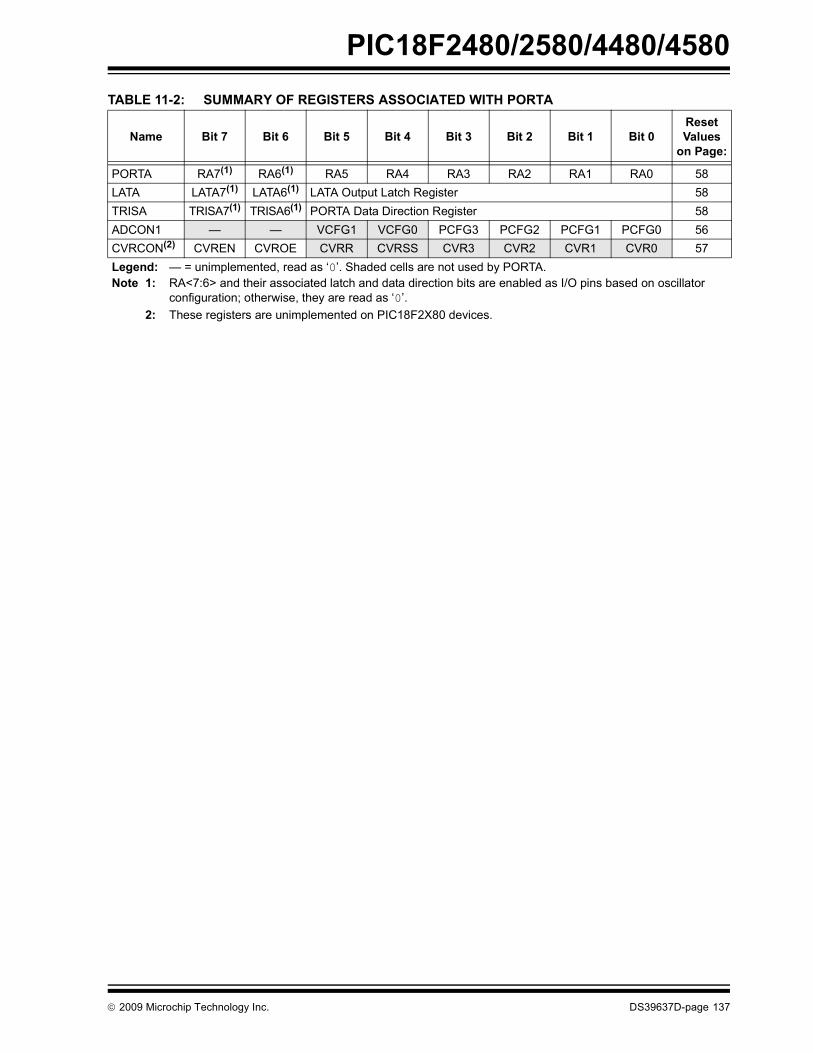
PIC18F2480/2580/4480/4580
TABLE 11-2: SUMMARY OF REGISTERS ASSOCIATED WITH PORTAName Bit 7 Bit 6 Bit 5 Bit 4 Bit 3 Bit 2 Bit 1 Bit 0Reset Values
on Page:
PORTA RA7(1) RA6(1) RA5 RA4 RA3 RA2 RA1 RA0 58LATA LATA7(1) LATA6(1) LATA Output Latch Register 58TRISA TRISA7(1) TRISA6(1) PORTA Data Direction Register 58ADCON1 — — VCFG1 VCFG0 PCFG3 PCFG2 PCFG1 PCFG0 56CVRCON(2) CVREN CVROE CVRR CVRSS CVR3 CVR2 CVR1 CVR0 57Legend: — = unimplemented, read as ‘0’. Shaded cells are not used by PORTA.Note 1: RA<7:6> and their associated latch and data direction bits are enabled as I/O pins based on oscillator
configuration; otherwise, they are read as ‘0’.2: These registers are unimplemented on PIC18F2X80 devices.
© 2009 Microchip Technology Inc. DS39637D-page 137

PIC18F2480/2580/4480/4580
11.2 PORTB, TRISB and LATBRegistersPORTB is an 8-bit wide, bidirectional port. The corre-sponding Data Direction register is TRISB. Setting aTRISB bit (= 1) will make the corresponding PORTBpin an input (i.e., put the corresponding output driver ina high-impedance mode). Clearing a TRISB bit (= 0)will make the corresponding PORTB pin an output (i.e.,put the contents of the output latch on the selected pin).
The Output Latch register (LATB) is also memorymapped. Read-modify-write operations on the LATBregister read and write the latched output value forPORTB.
Pins, RB2 through RB3, are multiplexed with the ECANperipheral. Refer to Section 24.0 “ECAN Module” forproper settings of TRISB when CAN is enabled.
EXAMPLE 11-2: INITIALIZING PORTB
Each of the PORTB pins has a weak internal pull-up. Asingle control bit can turn on all the pull-ups. This isperformed by clearing bit, RBPU (INTCON2<7>). Theweak pull-up is automatically turned off when the portpin is configured as an output. The pull-ups aredisabled on all device resets.
Four of the PORTB pins (RB<7:4>) have an interrupt-on-change feature. Only pins configured as inputs cancause this interrupt to occur (i.e., any RB<7:4> pinconfigured as an output is excluded from the interrupt-on-change comparison). The input pins (of RB<7:4>)are compared with the old value latched on the lastread of PORTB. The “mismatch” outputs of RB<7:4>are ORed together to generate the RB Port ChangeInterrupt with Flag bit, RBIF (INTCON<0>).
This interrupt can wake the device from Sleep. Theuser, in the Interrupt Service Routine, can clear theinterrupt in the following manner:
a) Any read or write of PORTB (except with theMOVFF (ANY), PORTB instruction). This willend the mismatch condition.
b) 1 TCY.c) Clear flag bit, RBIF.
A mismatch condition will continue to set flag bit, RBIF.Reading PORTB and waiting 1 TCY will end themismatch condition and allow flag bit, RBIF, to becleared.
The interrupt-on-change feature is recommended forwake-up on key depression operation and operationswhere PORTB is only used for the interrupt-on-changefeature. Polling of PORTB is not recommended whileusing the interrupt-on-change feature.
Note: On a Power-on Reset, RB4, RB1 and RB0are configured as analog inputs by defaultand read as ‘0’; RB<7:5> and RB<3:2>are configured as digital inputs.
CLRF PORTB ; Initialize PORTB by; clearing output; data latches
CLRF LATB ; Alternate method; to clear output; data latches
MOVLW 0Eh ; Set RB<4:0> asMOVWF ADCON1 ; digital I/O pins
; (required if config bit; PBADEN is set)
MOVLW 0CFh ; Value used to; initialize data ; direction
MOVWF TRISB ; Set RB<3:0> as inputs; RB<5:4> as outputs; RB<7:6> as inputs
DS39637D-page 138 © 2009 Microchip Technology Inc.

PIC18F2480/2580/4480/4580
TABLE 11-3: PORTB I/O SUMMARYPin Name Function I/O TRIS Buffer Description
RB0/INT0/FLT0/AN10 RB0 OUT 0 DIG LATB<0> data output.IN 1 TTL PORTB<0> data input. Weak pull-up available only in this mode.
INT0 IN 1 ST External Interrupt 0 input.FLT0(1) IN 1 ST Enhanced PWM Fault input.AN10 IN 1 ANA A/D Input Channel 10. Enabled on POR, this analog input overrides
the digital input (read as clear – low level).RB1/INT1/AN8 RB1 OUT 0 DIG LATB<1> data output.
IN 1 TTL PORTB<1> data input. Weak pull-up available only in this mode.INT1 IN 1 ST External Interrupt 1 input. AN8 IN 1 ANA A/D Input Channel 8. Enabled on POR; this analog input overrides
the digital input (read as clear – low level).RB2/INT2/CANTX RB2 OUT x DIG LATB<2> data output.
IN 1 TTL PORTB<2> data input. Weak pull-up available only in this mode.INT2 IN 1 ST External Interrupt 2 input.
CANTX OUT 1 DIG CAN transmit signal output. The CAN interface overrides the TRIS<2> control when enabled.
RB3/CANRX RB3 OUT 0 DIG LATB<3> data output.IN 1 TTL PORTB<3> data input. Weak pull-up available only in this mode.
CANRX IN 1 ST CAN receive signal input. Pin must be configured as a digital input by setting TRISB<3>.
RB4/KBI0/AN9 RB4 OUT 0 DIG LATB<4> data output.IN 1 TTL PORTB<4> data input. Weak pull-up available only in this mode.
KBI0 IN 1 TTL Interrupt-on-pin change.AN9 IN 1 ANA A/D Input Channel 9. Enabled on POR; this analog input overrides
the digital input (read as clear – low level).RB5/KBI1/PGM RB5 OUT 0 DIG LATB<5> data output.
IN 1 TTL PORTB<5> data input. Weak pull-up available only in this mode.KBI1 IN 1 TTL Interrupt-on-pin change.PGM IN x ST Low-Voltage Programming mode entry (ICSP™). Enabling this
function overrides digital output.RB6/KBI2/PGC RB6 OUT 0 DIG LATB<6> data output.
IN 1 TTL PORTB<6> data input. Weak pull-up available only in this mode.KBI2 IN 1 TTL Interrupt-on-pin change.PGC IN x ST Low-Voltage Programming mode entry (ICSP) clock input.
RB7/KBI3/PGD RB7 OUT 0 DIG LATB<7> data output.IN 1 TTL PORTB<7> data input. Weak pull-up available only in this mode.
KBI3 IN 1 TTL Interrupt-on-pin change.PGD OUT x DIG Low-Voltage Programming mode entry (ICSP) clock output.
IN x ST Low-Voltage Programming mode entry (ICSP) clock input.Legend: OUT = Output, IN = Input, ANA = Analog Signal, DIG = Digital Output, ST = Schmitt Buffer Input, TTL = TTL Buffer InputNote 1: Available on 40/44-pin devices only.
© 2009 Microchip Technology Inc. DS39637D-page 139

PIC18F2480/2580/4480/4580
TABLE 11-4: SUMMARY OF REGISTERS ASSOCIATED WITH PORTBName Bit 7 Bit 6 Bit 5 Bit 4 Bit 3 Bit 2 Bit 1 Bit 0Reset Values
on Page:
PORTB RB7 RB6 RB5 RB4 RB3 RB2 RB1 RB0 58LATB LATB Output Latch Register 58TRISB PORTB Data Direction Register 58INTCON GIE/GIEH PEIE/GIEL TMR0IE INT0IE RBIE TMR0IF INT0IF RBIF 55
INTCON2 RBPU INTEDG0 INTEDG1 INTEDG2 — TMR0IP — RBIP 55INTCON3 INT2IP INT1IP — INT2IE INT1IE — INT2IF INT1IF 55ADCON1 — — VCFG1 VCFG0 PCFG3 PCFG2 PCFG1 PCFG0 56Legend: — = unimplemented, read as ‘0’. Shaded cells are not used by PORTB.
DS39637D-page 140 © 2009 Microchip Technology Inc.

PIC18F2480/2580/4480/4580
11.3 PORTC, TRISC and LATCRegistersPORTC is an 8-bit wide, bidirectional port. The corre-sponding Data Direction register is TRISC. Setting aTRISC bit (= 1) will make the corresponding PORTCpin an input (i.e., put the corresponding output driver ina high-impedance mode). Clearing a TRISC bit (= 0)will make the corresponding PORTC pin an output (i.e.,put the contents of the output latch on the selected pin).
The Output Latch register (LATC) is also memorymapped. Read-modify-write operations on the LATCregister read and write the latched output value forPORTC.
PORTC is multiplexed with several peripheral functions(Table 11-5). The pins have Schmitt Trigger inputbuffers.
When enabling peripheral functions, care should betaken in defining TRIS bits for each PORTC pin. Someperipherals override the TRIS bit to make a pin an output,while other peripherals override the TRIS bit to make apin an input. The user should refer to the correspondingperipheral section for the correct TRIS bit settings.
The contents of the TRISC register are affected byperipheral overrides. Reading TRISC always returnsthe current contents, even though a peripheral devicemay be overriding one or more of the pins.
EXAMPLE 11-3: INITIALIZING PORTC
Note: On a Power-on Reset, these pins areconfigured as digital inputs.
CLRF PORTC ; Initialize PORTC by; clearing output; data latches
CLRF LATC ; Alternate method; to clear output; data latches
MOVLW 0CFh ; Value used to ; initialize data ; direction
MOVWF TRISC ; Set RC<3:0> as inputs; RC<5:4> as outputs; RC<7:6> as inputs
© 2009 Microchip Technology Inc. DS39637D-page 141

PIC18F2480/2580/4480/4580
TABLE 11-5: PORTC I/O SUMMARYTABLE 11-6: SUMMARY OF REGISTERS ASSOCIATED WITH PORTC
Pin Name Function I/O TRIS Buffer Description
RC0/T1OSO/T13CKI
RC0 OUT 0 DIG LATC<0> data output.IN 1 ST PORTC<0> data input.
T1OSO OUT x ANA Timer1 oscillator output – overrides the TRIS<0> control when enabled.T13CKI IN 1 ST Timer1/Timer3 clock input.
RC1/T1OSI RC1 OUT 0 DIG LATC<1> data output.IN 1 ST PORTC<1> data input.
T1OSI IN x ANA Timer1 oscillator input – overrides the TRIS<1> control when enabled.RC2/CCP1 RC2 OUT 0 DIG LATC<2> data output.
IN 1 ST PORTC<2> data input.CCP1 OUT 0 DIG CCP1 compare output.
IN 1 ST CCP1 capture input.RC3/SCK/SCL RC3 OUT 0 DIG LATC<3> data output.
IN 1 ST PORTC<3> data input.SCK OUT 0 DIG SPI clock output (MSSP module) – must have TRIS set to ‘1’ to allow
MSSP module to control the bidirectional communication.IN 1 ST SPI clock input (MSSP module).
SCL OUT 0 DIG I2C™/SM bus clock output (MSSP module) – must have TRIS set to ‘1’ to allow MSSP module to control the bidirectional communication.
IN 1 I2C™/SMB I2C/SM bus clock input.RC4/SDI/SDA RC4 OUT 0 DIG LATC<4> data output.
IN 1 ST PORTC<4> data input.SDI IN 1 ST SPI data input (MSSP module).SDA OUT 1 DIG I2C/SM bus data output (MSSP module) – must have TRIS set to ‘1’ to
allow MSSP module to control the bidirectional communication.IN 1 I2C/SMB I2C/SM bus data input (MSSP module) – must have TRIS set to ‘1’ to
allow MSSP module to control the bidirectional communication.RC5/SDO RC5 OUT 0 DIG LATC<5> data output.
IN 1 ST PORTC<5> data input.SDO OUT 0 DIG SPI data output (MSSP module).
RC6/TX/CK RC6 OUT 0 DIG LATC<6> data output.IN 1 ST PORTC<6> data input.
TX OUT 0 DIG EUSART data output.CK OUT 1 DIG EUSART synchronous clock output – must have TRIS set to ‘1’ to enable
EUSART to control the bidirectional communication.IN 1 ST EUSART synchronous clock input.
RC7/RX/DT RC7 OUT 0 DIG LATC<7> data output.IN 1 ST PORTC<7> data input.
RX IN 1 ST EUSART asynchronous data input.DT OUT 1 DIG EUSART synchronous data output – must have TRIS set to ‘1’ to enable
EUSART to control the bidirectional communication.IN 1 ST EUSART synchronous data input.
Legend: OUT = Output, IN = Input, ANA = Analog Signal, DIG = Digital Output, ST = Schmitt Buffer Input, TTL = TTL Buffer Input
Name Bit 7 Bit 6 Bit 5 Bit 4 Bit 3 Bit 2 Bit 1 Bit 0Reset Values
on Page:
PORTC RC7 RC6 RC5 RC4 RC3 RC2 RC1 RC0 58LATC LATC Output Latch Register 58TRISC PORTC Data Direction Register 58
DS39637D-page 142 © 2009 Microchip Technology Inc.

PIC18F2480/2580/4480/4580
11.4 PORTD, TRISD and LATDRegisters
PORTD is an 8-bit wide, bidirectional port. The corre-sponding Data Direction register is TRISD. Setting aTRISD bit (= 1) will make the corresponding PORTDpin an input (i.e., put the corresponding output driver ina high-impedance mode). Clearing a TRISD bit (= 0)will make the corresponding PORTD pin an output (i.e.,put the contents of the output latch on the selected pin).
The Output Latch register (LATD) is also memorymapped. Read-modify-write operations on the LATDregister read and write the latched output value forPORTD.
All pins on PORTD are implemented with SchmittTrigger input buffers. Each pin is individuallyconfigurable as an input or output.
Four of the PORTD pins are multiplexed with outputsP1A, P1B, P1C and P1D of the Enhanced CCPmodule. The operation of these additional PWM outputpins is covered in greater detail in Section 17.0“Enhanced Capture/Compare/PWM (ECCP)Module”.
Four of the PORTD pins are multiplexed with the inputpins of the comparators. The operation of these inputpins is covered in greater detail in Section 21.0“Comparator Module”.
PORTD can also be configured as an 8-bit wide micro-processor port (Parallel Slave Port) by setting controlbit, PSPMODE (TRISE<4>). In this mode, the inputbuffers are TTL. See Section 11.6 “Parallel SlavePort” for additional information on the Parallel SlavePort (PSP).
EXAMPLE 11-4: INITIALIZING PORTD
Note: PORTD is only available on PIC18F4X80devices.
Note: On a Power-on Reset, these pins areconfigured as analog inputs.
CLRF PORTD ; Initialize PORTD by ; clearing output ; data latchesCLRF LATD ; Alternate method
; to clear output; data latches
MOVLW 0CFh ; Value used to ; initialize data ; direction
MOVWF TRISD ; Set RD<3:0> as inputs; RD<5:4> as outputs; RD<7:6> as inputs
© 2009 Microchip Technology Inc. DS39637D-page 143

PIC18F2480/2580/4480/4580
TABLE 11-7: PORTD I/O SUMMARYPin Name Function I/O TRIS Buffer Description
RD0/PSP0/C1IN+
RD0 OUT 0 DIG LATD<0> data output.IN 1 ST PORTD<0> data input.
PSP0 OUT x DIG Parallel Slave Port (PSP) data output (overrides the TRIS<0> control when enabled).IN x TTL Parallel Slave Port (PSP) data input (overrides the TRIS<0> control when enabled).
C1IN+ IN 1 ANA Comparator 1 Positive Input B. Default on POR. This analog input overrides the digital input (read as clear – low level).
RD1/PSP1/C1IN-
RD1 OUT 0 DIG LATD<1> data output.IN 1 ST PORTD<1> data input.
PSP1 OUT x DIG Parallel Slave Port (PSP) data output (overrides the TRIS<1> control when enabled).
IN x TTL Parallel Slave Port (PSP) data input (overrides the TRIS<1> control when enabled).C1IN- IN 1 ANA Comparator 1 negative input. Default on POR. This analog input overrides the
digital input (read as clear – low level).RD2/PSP2/C2IN+
RD2 OUT 0 DIG LATD<2> data output.IN 1 ST PORTD<2> data input.
PSP2 OUT x DIG Parallel Slave Port (PSP) data output (overrides the TRIS<2> control when enabled).
IN x TTL Parallel Slave Port (PSP) data input (overrides the TRIS<2> control when enabled).C2IN+ IN 1 ANA Comparator 2 positive input. Default on POR. This analog input overrides the digital
input (read as clear – low level).RD3/PSP3/C2IN-
RD3 OUT 0 DIG LATD<3> data output.IN 1 ST PORTD<3> data input.
PSP3 OUT x DIG Parallel Slave Port (PSP) data output (overrides the TRIS<3> control when enabled).IN x TTL Parallel Slave Port (PSP) data input (overrides the TRIS<3> control when enabled).
C2IN- IN 1 ANA Comparator 2 negative input. Default input on POR. This analog input overrides the digital input (read as clear – low level).
RD4/PSP4/ECCP1/P1A
RD4 OUT 0 DIG LATD<4> data output.IN 1 ST PORTD<4> data input.
PSP4 OUT x DIG Parallel Slave Port (PSP) data output (overrides the TRIS<4> control when enabled).IN x TTL Parallel Slave Port (PSP) data input (overrides the TRIS<4> control when enabled).
ECCP1 OUT 0 DIG ECCP1 compare output.IN 1 ST ECCP1 capture input.
P1A OUT 0 DIG ECCP1 Enhanced PWM output, Channel A.RD5/PSP5/P1B
RD5 OUT 0 DIG LATD<5> data output.IN 1 ST PORTD<5> data input.
PSP5 OUT X DIG Parallel Slave Port (PSP) data output (overrides the TRIS<5> control when enabled).IN x TTL Parallel Slave Port (PSP) data input (overrides the TRIS<5> control when enabled).
P1B OUT 0 DIG ECCP1 Enhanced PWM output, Channel B.RD6/PSP6/P1C
RD6 OUT 0 DIG LATD<6> data output.IN 1 ST PORTD<6> data input.
PSP6 OUT x DIG Parallel Slave Port (PSP) data output (overrides the TRIS<6> control when enabled).IN x TTL Parallel Slave Port (PSP) data input (overrides the TRIS<6> control when enabled).
P1C OUT 0 DIG ECCP1 Enhanced PWM output, Channel C.RD7/PSP7/P1D
RD7 OUT 0 DIG LATD<7> data output.IN 1 ST PORTD<7> data input.
PSP7 OUT x DIG Parallel Slave Port (PSP) data output (overrides the TRIS<7> control when enabled).IN x TTL Parallel Slave Port (PSP) data input (overrides the TRIS<7> control when enabled).
P1D OUT 0 DIG ECCP1 Enhanced PWM output, channel D.Legend: OUT = Output, IN = Input, ANA = Analog Signal, DIG = Digital Output, ST = Schmitt Buffer Input, TTL = TTL Buffer Input
DS39637D-page 144 © 2009 Microchip Technology Inc.

PIC18F2480/2580/4480/4580
TABLE 11-8: SUMMARY OF REGISTERS ASSOCIATED WITH PORTDName Bit 7 Bit 6 Bit 5 Bit 4 Bit 3 Bit 2 Bit 1 Bit 0Reset Values
on Page:
PORTD(1) RD7 RD6 RD5 RD4 RD3 RD2 RD1 RD0 58LATD(1) LATD Output Latch Register 58TRISD(1) PORTD Data Direction Register 58TRISE(1) IBF OBF IBOV PSPMODE — TRISE2 TRISE1 TRISE0 58ECCP1CON(1) EPWM1M1 EPWM1M0 EDC1B1 EDC1B0 ECCP1M3 ECCP1M2 ECCP1M1 ECCP1M0 57Legend: — = unimplemented, read as ‘0’. Shaded cells are not used by PORTD.Note 1: These registers are available on PIC18F4X80 devices only.
© 2009 Microchip Technology Inc. DS39637D-page 145

PIC18F2480/2580/4480/4580
11.5 PORTE, TRISE and LATERegistersDepending on the particular PIC18F2480/2580/4480/4580 device selected, PORTE is implemented in twodifferent ways.For PIC18F4X80 devices, PORTE is a 4-bit wide port.Three pins (RE0/RD/AN5, RE1/WR/AN6/C1OUT andRE2/CS/AN7/C2OUT) are individually configurable asinputs or outputs. These pins have Schmitt Triggerinput buffers. When selected as an analog input, thesepins will read as ‘0’s.The corresponding Data Direction register is TRISE.Setting a TRISE bit (= 1) will make the correspondingPORTE pin an input (i.e., put the corresponding outputdriver in a high-impedance mode). Clearing a TRISE bit(= 0) will make the corresponding PORTE pin an output(i.e., put the contents of the output latch on the selectedpin).TRISE controls the direction of the RE pins, even whenthey are being used as analog inputs. The user mustmake sure to keep the pins configured as inputs whenusing them as analog inputs.
The upper four bits of the TRISE register also controlthe operation of the Parallel Slave Port. Their operationis explained in Register 11-1.The Output Latch register (LATE) is also memorymapped. Read-modify-write operations on the LATEregister, read and write the latched output value forPORTE.
The fourth pin of PORTE (MCLR/VPP/RE3) is an inputonly pin. Its operation is controlled by the MCLREConfiguration bit. When selected as a port pin(MCLRE = 0), it functions as a digital input only pin. Assuch, it does not have TRIS or LAT bits associated withits operation. Otherwise, it functions as the device’sMaster Clear input. In either configuration, RE3 alsofunctions as the programming voltage input duringprogramming.
EXAMPLE 11-5: INITIALIZING PORTE
11.5.1 PORTE IN 28-PIN DEVICESFor PIC18F2X80 devices, PORTE is only availablewhen Master Clear functionality is disabled(MCLRE = 0). In these cases, PORTE is a single bit,input only port comprised of RE3 only. The pin operatesas previously described.
Note: On a Power-on Reset, RE<2:0> areconfigured as analog inputs.
Note: On a Power-on Reset, RE3 is enabled asa digital input only if Master Clearfunctionality is disabled.
CLRF PORTE ; Initialize PORTE by; clearing output; data latches
CLRF LATE ; Alternate method; to clear output; data latches
MOVLW 0Ah ; Configure A/D MOVWF ADCON1 ; for digital inputsMOVLW 03h ; Value used to
; initialize data ; direction
MOVLW 07h ; Turn offMOVWF CMCON ; comparatorsMOVWF TRISC ; Set RE<0> as inputs
; RE<1> as outputs; RE<2> as inputs
DS39637D-page 146 © 2009 Microchip Technology Inc.
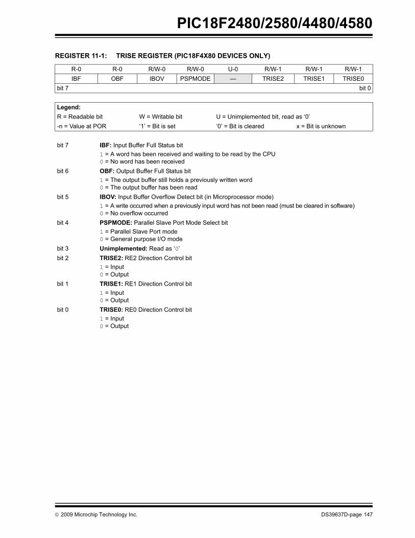
PIC18F2480/2580/4480/4580
REGISTER 11-1: TRISE REGISTER (PIC18F4X80 DEVICES ONLY)R-0 R-0 R/W-0 R/W-0 U-0 R/W-1 R/W-1 R/W-1IBF OBF IBOV PSPMODE — TRISE2 TRISE1 TRISE0
bit 7 bit 0
Legend:R = Readable bit W = Writable bit U = Unimplemented bit, read as ‘0’-n = Value at POR ‘1’ = Bit is set ‘0’ = Bit is cleared x = Bit is unknown
bit 7 IBF: Input Buffer Full Status bit1 = A word has been received and waiting to be read by the CPU0 = No word has been received
bit 6 OBF: Output Buffer Full Status bit1 = The output buffer still holds a previously written word 0 = The output buffer has been read
bit 5 IBOV: Input Buffer Overflow Detect bit (in Microprocessor mode)1 = A write occurred when a previously input word has not been read (must be cleared in software)0 = No overflow occurred
bit 4 PSPMODE: Parallel Slave Port Mode Select bit1 = Parallel Slave Port mode 0 = General purpose I/O mode
bit 3 Unimplemented: Read as ‘0’bit 2 TRISE2: RE2 Direction Control bit
1 = Input 0 = Output
bit 1 TRISE1: RE1 Direction Control bit 1 = Input 0 = Output
bit 0 TRISE0: RE0 Direction Control bit 1 = Input 0 = Output
© 2009 Microchip Technology Inc. DS39637D-page 147

PIC18F2480/2580/4480/4580
TABLE 11-9: PORTE I/O SUMMARYTABLE 11-10: SUMMARY OF REGISTERS ASSOCIATED WITH PORTE
Pin Name Function I/O TRIS Buffer Description
RE0/RD/AN5 RE0 OUT 0 DIG LATE<0> data output.IN 1 ST PORTE<0> data input.
RD IN 1 TTL PSP read enable input.AN5 IN 1 ANA A/D Input Channel 5. Enabled on POR; this analog input overrides the
digital input (read as clear – low level).
RE1/WR/AN6/C1OUT RE1 OUT 0 DIG LATE<1> data output.IN 1 ST PORTE<1> data input.
WR IN 1 TTL PSP write enable input.AN6 IN 1 ANA A/D Input Channel 6. Enabled on POR; this analog input overrides the
digital input (read as clear – low level).C1OUT OUT 0 DIG Comparator 1 output.
RE2/CS/AN7/C2OUT RE2 OUT 0 DIG LATE<2> data output.IN 1 ST PORTE<2> data input.
CS IN 1 TTL PSP chip select input.AN7 IN 1 ANA A/D Input Channel 7. Enabled on POR; this analog input overrides the
digital input (read as clear – low level).C2OUT OUT 0 DIG Comparator 2 output.
MCLR/VPP/RE3 MCLR IN x ST External Reset input. Disabled when MCLRE Configuration bit is ‘1’.VPP IN x ANA High-voltage detection; used by ICSP™ operation.RE3 IN 1 ST PORTE<3> data input. Disabled when MCLRE Configuration bit is ‘0’.
Legend: PWR = Power Supply, OUT = Output, IN = Input, ANA = Analog Signal, DIG = Digital Output, ST = Schmitt Buffer Input, TTL = TTL Buffer Input
Name Bit 7 Bit 6 Bit 5 Bit 4 Bit 3 Bit 2 Bit 1 Bit 0Reset Values
on Page:
PORTE(3) — — — — RE3(1,2) RE2 RE1 RE0 58LATE(2) — — — — — LATE Output Latch Register 58TRISE(3) IBF OBF IBOV PSPMODE — TRISE2 TRISE1 TRISE0 58ADCON1 — — VCFG1 VCFG0 PCFG3 PCFG2 PCFG1 PCFG0 56CMCON(3) C2OUT C1OUT C2INV C1INV CIS CM2 CM1 CM0 57Legend: — = unimplemented, read as ‘0’. Shaded cells are not used by PORTE.Note 1: Implemented only when Master Clear functionality is disabled (MCLRE Configuration bit = 0).
2: RE3 is the only PORTE bit implemented on both PIC18F2X80 and PIC18F4X80 devices. All other bits are implemented only when PORTE is implemented (i.e., PIC18F4X80 devices).
3: These registers are unimplemented on PIC18F2X80 devices.
DS39637D-page 148 © 2009 Microchip Technology Inc.

PIC18F2480/2580/4480/4580
11.6 Parallel Slave PortIn addition to its function as a general I/O port, PORTDcan also operate as an 8-bit wide Parallel Slave Port(PSP) or microprocessor port. PSP operation is con-trolled by the 4 upper bits of the TRISE register(Register 11-1). Setting control bit, PSPMODE(TRISE<4>), enables PSP operation, as long as theEnhanced CCP module is not operating in dual outputor quad output PWM mode. In Slave mode, the port isasynchronously readable and writable by the externalworld.
The PSP can directly interface to an 8-bit micro-processor data bus. The external microprocessor canread or write the PORTD latch as an 8-bit latch. Settingthe control bit PSPMODE enables the PORTE I/O pinsto become control inputs for the microprocessor port.When set, port pin RE0 is the RD input, RE1 is the WRinput and RE2 is the CS (Chip Select) input. For thisfunctionality, the corresponding data direction bits ofthe TRISE register (TRISE<2:0>) must be configuredas inputs (set). The A/D port Configuration bits,PFCG<3:0> (ADCON1<3:0>), must also be set to‘1010’.
A write to the PSP occurs when both the CS and WRlines are first detected low and ends when either aredetected high. The PSPIF and IBF flag bits are both setwhen the write ends.
A read from the PSP occurs when both the CS and RDlines are first detected low. The data in PORTD is readout and the OBF bit is set. If the user writes new datato PORTD to set OBF, the data is immediately read out;however, the OBF bit is not set.
When either the CS or RD lines are detected high, thePORTD pins return to the input state and the PSPIF bitis set. User applications should wait for PSPIF to be setbefore servicing the PSP; when this happens, the IBFand OBF bits can be polled and the appropriate actiontaken.
The timing for the control signals in Write and Readmodes is shown in Figure 11-3 and Figure 11-4,respectively.
FIGURE 11-2: PORTD AND PORTE BLOCK DIAGRAM (PARALLEL SLAVE PORT)
Note: The Parallel Slave Port is only available onPIC18F4X80 devices.
Data Bus
WR LATD RDx pin
QD
CK
EN
Q D
ENRD PORTD
One bit of PORTD
Set Interrupt FlagPSPIF (PIR1<7>)
Read
Chip Select
Write
RD
CS
WR
TTL
TTL
TTL
TTL
orWR PORTD
RD LATD
Data Latch
Note: I/O pins have diode protection to VDD and VSS.
PORTE Pins
© 2009 Microchip Technology Inc. DS39637D-page 149

PIC18F2480/2580/4480/4580
FIGURE 11-3: PARALLEL SLAVE PORT WRITE WAVEFORMSFIGURE 11-4: PARALLEL SLAVE PORT READ WAVEFORMS
TABLE 11-11: REGISTERS ASSOCIATED WITH PARALLEL SLAVE PORT
Name Bit 7 Bit 6 Bit 5 Bit 4 Bit 3 Bit 2 Bit 1 Bit 0Reset Values
on Page:
PORTD(1) RD7 RD6 RD5 RD4 RD3 RD2 RD1 RD0 58LATD(1) LATD Output Latch Register 58TRISD(1) PORTD Data Direction Register 58PORTE(1) — — — — RE3 RE2 RE1 RE0 58LATE(1) — — — — — LATE Output Latch Register 58TRISE(1) IBF OBF IBOV PSPMODE — TRISE2 TRISE1 TRISE0 58INTCON GIE/GIEH PEIE/GIEL TMR0IE INT0IE RBIE TMR0IF INT0IF RBIF 55PIR1 PSPIF ADIF RCIF TXIF SSPIF CCP1IF TMR2IF TMR1IF 58PIE1 PSPIE ADIE RCIE TXIE SSPIE CCP1IE TMR2IE TMR1IE 58IPR1 PSPIP ADIP RCIP TXIP SSPIP CCP1IP TMR2IP TMR1IP 58ADCON1 — — VCFG1 VCFG0 PCFG3 PCFG2 PCFG1 PCFG0 56CMCON(1) C2OUT C1OUT C2INV C1INV CIS CM2 CM1 CM0 57Legend: — = unimplemented, read as ‘0’. Shaded cells are not used by the Parallel Slave Port.Note 1: These registers are available on PIC18F4X80 devices only.
Q1 Q2 Q3 Q4
CS
Q1 Q2 Q3 Q4 Q1 Q2 Q3 Q4
WR
RD
IBF
OBF
PSPIF
PORTD<7:0>
Q1 Q2 Q3 Q4
CS
Q1 Q2 Q3 Q4 Q1 Q2 Q3 Q4
WR
IBF
PSPIF
RD
OBF
PORTD<7:0>
DS39637D-page 150 © 2009 Microchip Technology Inc.

PIC18F2480/2580/4480/4580
12.0 TIMER0 MODULEThe Timer0 module incorporates the following features:
• Software-selectable operation as a timer or counter in both 8-bit or 16-bit modes
• Readable and writable registers• Dedicated 8-bit, software programmable
prescaler• Selectable clock source (internal or external)• Edge select for external clock• Interrupt-on-overflow
The T0CON register (Register 12-1) controls allaspects of the module’s operation, including theprescale selection. It is both readable and writable.
A simplified block diagram of the Timer0 module in 8-bitmode is shown in Figure 12-1. Figure 12-2 shows asimplified block diagram of the Timer0 module in 16-bitmode.
REGISTER 12-1: T0CON: TIMER0 CONTROL REGISTER
R/W-1 R/W-1 R/W-1 R/W-1 R/W-1 R/W-1 R/W-1 R/W-1TMR0ON T08BIT T0CS T0SE PSA T0PS2 T0PS1 T0PS0
bit 7 bit 0
Legend:R = Readable bit W = Writable bit U = Unimplemented bit, read as ‘0’-n = Value at POR ‘1’ = Bit is set ‘0’ = Bit is cleared x = Bit is unknown
bit 7 TMR0ON: Timer0 On/Off Control bit 1 = Enables Timer0 0 = Stops Timer0
bit 6 T08BIT: Timer0 8-Bit/16-Bit Control bit 1 = Timer0 is configured as an 8-bit timer/counter 0 = Timer0 is configured as a 16-bit timer/counter
bit 5 T0CS: Timer0 Clock Source Select bit 1 = Transition on T0CKI pin input edge0 = Internal clock (FOSC/4)
bit 4 T0SE: Timer0 Source Edge Select bit1 = Increment on high-to-low transition on T0CKI pin 0 = Increment on low-to-high transition on T0CKI pin
bit 3 PSA: Timer0 Prescaler Assignment bit 1 = TImer0 prescaler is not assigned. Timer0 clock input bypasses prescaler. 0 = Timer0 prescaler is assigned. Timer0 clock input comes from prescaler output.
bit 2-0 T0PS<2:0>: Timer0 Prescaler Select bits 111 = 1:256 Prescale value110 = 1:128 Prescale value101 = 1:64 Prescale value100 = 1:32 Prescale value011 = 1:16 Prescale value010 = 1:8 Prescale value001 = 1:4 Prescale value000 = 1:2 Prescale value
© 2009 Microchip Technology Inc. DS39637D-page 151

PIC18F2480/2580/4480/4580
12.1 Timer0 OperationTimer0 can operate as either a timer or a counter; themode is selected by clearing the T0CS bit(T0CON<5>). In Timer mode, the module incrementson every clock by default unless a different prescalervalue is selected (see Section 12.3 “Prescaler”). Ifthe TMR0 register is written to, the increment is inhib-ited for the following two instruction cycles. The usercan work around this by writing an adjusted value to theTMR0 register.The Counter mode is selected by setting the T0CS bit(= 1). In Counter mode, Timer0 increments either onevery rising or falling edge of pin, RA4/T0CKI. Theincrementing edge is determined by the Timer0 SourceEdge Select bit, T0SE (T0CON<4>); clearing this bitselects the rising edge. Restrictions on the externalclock input are discussed below.
An external clock source can be used to drive Timer0;however, it must meet certain requirements to ensurethat the external clock can be synchronized with the
internal phase clock (TOSC). There is a delay betweensynchronization and the onset of incrementing thetimer/counter.
12.2 Timer0 Reads and Writes in 16-Bit Mode
TMR0H is not the actual high byte of Timer0 in 16-bitmode; it is actually a buffered version of the real highbyte of Timer0, which is not directly readable norwritable (refer to Figure 12-2). TMR0H is updated withthe contents of the high byte of Timer0 during a read ofTMR0L. This provides the ability to read all 16 bits ofTimer0 without having to verify that the read of the highand low byte were valid, due to a rollover betweensuccessive reads of the high and low byte.
Similarly, a write to the high byte of Timer0 must alsotake place through the TMR0H Buffer register. The highbyte is updated with the contents of TMR0H when awrite occurs to TMR0L. This allows all 16 bits of Timer0to be updated at once.
FIGURE 12-1: TIMER0 BLOCK DIAGRAM (8-BIT MODE)
FIGURE 12-2: TIMER0 BLOCK DIAGRAM (16-BIT MODE)
Note: Upon Reset, Timer0 is enabled in 8-bit mode with clock input from T0CKI max. prescale.
T0CKI pin
T0SE
0
1
1
0
T0CS
FOSC/4
ProgrammablePrescaler
Sync withInternalClocks
TMR0L
(2 TCY Delay)
Internal Data BusPSAT0PS<2:0>
Set TMR0IF
on Overflow
3 8
8
Note: Upon Reset, Timer0 is enabled in 8-bit mode with clock input from T0CKI max. prescale.
T0CKI pin
T0SE
0
1
1
0
T0CS
FOSC/4
ProgrammablePrescaler
Sync withInternalClocks
TMR0L
(2 TCY Delay)
Internal Data Bus
8
PSAT0PS<2:0>
Set TMR0IF
on Overflow
3
TMR0
TMR0H
High Byte
88
8
Read TMR0L
Write TMR0L
8
DS39637D-page 152 © 2009 Microchip Technology Inc.

PIC18F2480/2580/4480/4580
12.3 PrescalerAn 8-bit counter is available as a prescaler for the Timer0module. The prescaler is not directly readable or writable;its value is set by the PSA and T0PS<2:0> bits(T0CON<3:0>) which determine the prescalerassignment and prescale ratio.Clearing the PSA bit assigns the prescaler to theTimer0 module. When it is assigned, prescale valuesfrom 1:2 through 1:256 in power-of-2 increments areselectable.
When assigned to the Timer0 module, all instructionswriting to the TMR0 register (e.g., CLRF TMR0, MOVWFTMR0, BSF TMR0, etc.) clear the prescaler count.
12.3.1 SWITCHING PRESCALER ASSIGNMENT
The prescaler assignment is fully under softwarecontrol and can be changed “on-the-fly” during programexecution.
12.4 Timer0 InterruptThe TMR0 interrupt is generated when the TMR0register overflows from FFh to 00h in 8-bit mode, orfrom FFFFh to 0000h in 16-bit mode. This overflow setsthe TMR0IF flag bit. The interrupt can be masked byclearing the TMR0IE bit (INTCON<5>). Before re-enabling the interrupt, the TMR0IF bit must be clearedin software by the Interrupt Service Routine.
Since Timer0 is shut down in Sleep mode, the TMR0interrupt cannot awaken the processor from Sleep.
TABLE 12-1: REGISTERS ASSOCIATED WITH TIMER0
Note: Writing to TMR0 when the prescaler isassigned to Timer0 will clear the prescalercount but will not change the prescalerassignment.
Name Bit 7 Bit 6 Bit 5 Bit 4 Bit 3 Bit 2 Bit 1 Bit 0Reset Values
on Page:
TMR0L Timer0 Register Low Byte 56
TMR0H Timer0 Register High Byte 56
INTCON GIE/GIEH PEIE/GIEL TMR0IE INT0IE RBIE TMR0IF INT0IF RBIF 55
T0CON TMR0ON T08BIT T0CS T0SE PSA T0PS2 T0PS1 T0PS0 56
TRISA TRISA7(1) TRISA6(1) PORTA Data Direction Register 58
Legend: — = unimplemented locations, read as ‘0’. Shaded cells are not used by Timer0.Note 1: RA6/RA7 and their associated latch and direction bits are individually configured as port pins based on various
primary oscillator modes. When disabled, these bits read as ‘0’.
© 2009 Microchip Technology Inc. DS39637D-page 153

PIC18F2480/2580/4480/4580
NOTES:DS39637D-page 154 © 2009 Microchip Technology Inc.

PIC18F2480/2580/4480/4580
13.0 TIMER1 MODULEThe Timer1 timer/counter module incorporates thesefeatures:
• Software-selectable operation as a 16-bit timer or counter
• Readable and writable 8-bit registers (TMR1H and TMR1L)
• Selectable clock source (internal or external) with device clock or Timer1 oscillator internal options
• Interrupt-on-overflow• Module Reset on CCP Special Event Trigger• Device clock status flag (T1RUN)
A simplified block diagram of the Timer1 module isshown in Figure 13-1. A block diagram of the module’soperation in Read/Write mode is shown in Figure 13-2.
The module incorporates its own low-power oscillatorto provide an additional clocking option. The Timer1oscillator can also be used as a low-power clock sourcefor the microcontroller in power-managed operation.
Timer1 can also be used to provide Real-Time Clock(RTC) functionality to applications with only a minimaladdition of external components and code overhead.
Timer1 is controlled through the T1CON Controlregister (Register 13-1). It also contains the Timer1Oscillator Enable bit (T1OSCEN). Timer1 can beenabled or disabled by setting or clearing control bit,TMR1ON (T1CON<0>).
REGISTER 13-1: T1CON: TIMER1 CONTROL REGISTER
R/W-0 R-0 R/W-0 R/W-0 R/W-0 R/W-0 R/W-0 R/W-0
RD16 T1RUN T1CKPS1 T1CKPS0 T1OSCEN T1SYNC TMR1CS TMR1ONbit 7 bit 0
Legend:R = Readable bit W = Writable bit U = Unimplemented bit, read as ‘0’-n = Value at POR ‘1’ = Bit is set ‘0’ = Bit is cleared x = Bit is unknown
bit 7 RD16: 16-Bit Read/Write Mode Enable bit1 = Enables register read/write of Timer1 in one 16-bit operation0 = Enables register read/write of Timer1 in two 8-bit operations
bit 6 T1RUN: Timer1 System Clock Status bit1 = Device clock is derived from Timer1 oscillator0 = Device clock is derived from another source
bit 5-4 T1CKPS<1:0>: Timer1 Input Clock Prescale Select bits11 = 1:8 Prescale value 10 = 1:4 Prescale value 01 = 1:2 Prescale value 00 = 1:1 Prescale value
bit 3 T1OSCEN: Timer1 Oscillator Enable bit1 = Timer1 oscillator is enabled 0 = Timer1 oscillator is shut off The oscillator inverter and feedback resistor are turned off to eliminate power drain.
bit 2 T1SYNC: Timer1 External Clock Input Synchronization Select bitWhen TMR1CS = 1: 1 = Do not synchronize external clock input 0 = Synchronize external clock inputWhen TMR1CS = 0: This bit is ignored. Timer1 uses the internal clock when TMR1CS = 0.
bit 1 TMR1CS: Timer1 Clock Source Select bit1 = External clock from pin RC0/T1OSO/T13CKI (on the rising edge) 0 = Internal clock (FOSC/4)
bit 0 TMR1ON: Timer1 On bit1 = Enables Timer1 0 = Stops Timer1
© 2009 Microchip Technology Inc. DS39637D-page 155

PIC18F2480/2580/4480/4580
13.1 Timer1 OperationTimer1 can operate in one of these modes:• Timer• Synchronous Counter• Asynchronous Counter
The operating mode is determined by the clock selectbit, TMR1CS (T1CON<1>). When TMR1CS is cleared(= 0), Timer1 increments on every internal instruction
cycle (FOSC/4). When the bit is set, Timer1 incrementson every rising edge of the Timer1 external clock inputor the Timer1 oscillator, if enabled.
When Timer1 is enabled, the RC1/T1OSI and RC0/T1OSO/T13CKI pins become inputs. This means thevalues of TRISC<1:0> are ignored and the pins areread as ‘0’.
FIGURE 13-1: TIMER1 BLOCK DIAGRAM
FIGURE 13-2: TIMER1 BLOCK DIAGRAM (16-BIT READ/WRITE MODE)
T1SYNC
TMR1CS
T1CKPS<1:0>
Sleep InputT1OSCEN(1)
FOSC/4InternalClock
On/Off
Prescaler1, 2, 4, 8
SynchronizeDetect
1
02
T1OSO/T13CKI
T1OSI
1
0
TMR1ON
TMR1LSet
TMR1IFon Overflow
TMR1 High ByteClear TMR1
(CCP Special Event Trigger)
Timer1 Oscillator
Note 1: When enable bit, T1OSCEN, is cleared, the inverter and feedback resistor are turned off to eliminate power drain.
On/OffTimer1
T1SYNC
TMR1CS
T1CKPS<1:0>
Sleep InputT1OSCEN(1)
FOSC/4InternalClock
Prescaler1, 2, 4, 8
SynchronizeDetect
1
02
T1OSO/T13CKI
T1OSI
Note 1: When enable bit, T1OSCEN, is cleared, the inverter and feedback resistor are turned off to eliminate power drain.
1
0
TMR1L
Internal Data Bus
8
Set TMR1IF
on Overflow
TMR1
TMR1H
High Byte
88
8
Read TMR1L
Write TMR1L
8
TMR1ON
Clear TMR1(CCP Special Event Trigger)
Timer1 Oscillator
On/OffTimer1
1
DS39637D-page 156 © 2009 Microchip Technology Inc.

PIC18F2480/2580/4480/4580
13.2 Timer1 16-Bit Read/Write ModeTimer1 can be configured for 16-bit reads and writes(see Figure 13-2). When the RD16 control bit(T1CON<7>) is set, the address for TMR1H is mappedto a buffer register for the high byte of Timer1. A readfrom TMR1L will load the contents of the high byte ofTimer1 into the Timer1 High Byte Buffer register. Thisprovides the user with the ability to accurately read all16 bits of Timer1 without having to determine whethera read of the high byte, followed by a read of the lowbyte, has become invalid due to a rollover betweenreads.A write to the high byte of Timer1 must also take placethrough the TMR1H Buffer register. The Timer1 highbyte is updated with the contents of TMR1H when awrite occurs to TMR1L. This allows a user to write all16 bits to both the high and low bytes of Timer1 at once.
The high byte of Timer1 is not directly readable orwritable in this mode. All reads and writes must takeplace through the Timer1 High Byte Buffer register.Writes to TMR1H do not clear the Timer1 prescaler.The prescaler is only cleared on writes to TMR1L.
13.3 Timer1 OscillatorAn on-chip crystal oscillator circuit is incorporatedbetween pins, T1OSI (input) and T1OSO (amplifieroutput). It is enabled by setting the Timer1 OscillatorEnable bit, T1OSCEN (T1CON<3>). The oscillator is alow-power circuit rated for 32 kHz crystals. It willcontinue to run during all power-managed modes. Thecircuit for a typical LP oscillator is shown in Figure 13-3.Table 13-1 shows the capacitor selection for the Timer1oscillator.
The user must provide a software time delay to ensureproper start-up of the Timer1 oscillator.
FIGURE 13-3: EXTERNAL COMPONENTS FOR THE TIMER1 LP OSCILLATOR
TABLE 13-1: CAPACITOR SELECTION FOR THE TIMER OSCILLATOR(1-4)
13.3.1 USING TIMER1 AS A CLOCK SOURCE
The Timer1 oscillator is also available as a clock sourcein power-managed modes. By setting the clock selectbits, SCS<1:0> (OSCCON<1:0>), to ‘01’, the deviceswitches to SEC_RUN mode; both the CPU andperipherals are clocked from the Timer1 oscillator. If theIDLEN bit (OSCCON<7>) is cleared and a SLEEPinstruction is executed, the device enters SEC_IDLEmode. Additional details are available in Section 4.0“Power-Managed Modes”.
Whenever the Timer1 oscillator is providing the clocksource, the Timer1 system clock status flag, T1RUN(T1CON<6>), is set. This can be used to determine thecontroller’s current clocking mode. It can also indicatethe clock source being currently used by the Fail-SafeClock Monitor. If the Clock Monitor is enabled and theTimer1 oscillator fails while providing the clock, pollingthe T1RUN bit will indicate whether the clock is beingprovided by the Timer1 oscillator or another source.
13.3.2 LOW-POWER TIMER1 OPTION The Timer1 oscillator can operate at two distinct levelsof power consumption based on device configuration.When the LPT1OSC Configuration bit is set, the Timer1oscillator operates in a low-power mode. WhenLPT1OSC is not set, Timer1 operates at a higher powerlevel. Power consumption for a particular mode is rela-tively constant, regardless of the device’s operatingmode. The default Timer1 configuration is the higherpower mode.
As the low-power Timer1 mode tends to be moresensitive to interference, high noise environments maycause some oscillator instability. The low-power optionis, therefore, best suited for low noise applicationswhere power conservation is an important designconsideration.
Note: See the Notes with Table 13-1 for additionalinformation about capacitor selection.
C1
C2
XTAL
PIC18FXXXXT1OSI
T1OSO
32.768 kHz
33 pF
33 pF
Osc Type Freq C1 C2LP 32 kHz 27 pF 27 pF
Note 1: Microchip suggests these values as astarting point in validating the oscillatorcircuit.
2: Higher capacitance increases the stabilityof the oscillator but also increases thestart-up time.
3: Since each resonator/crystal has its owncharacteristics, the user should consultthe resonator/crystal manufacturer forappropriate values of externalcomponents.
4: Capacitor values are for design guidanceonly.
© 2009 Microchip Technology Inc. DS39637D-page 157

PIC18F2480/2580/4480/4580
13.3.3 TIMER1 OSCILLATOR LAYOUTCONSIDERATIONS
The Timer1 oscillator circuit draws very little powerduring operation. Due to the low-power nature of theoscillator, it may also be sensitive to rapidly changingsignals in close proximity.
The oscillator circuit, shown in Figure 13-3, should belocated as close as possible to the microcontroller.There should be no circuits passing within the oscillatorcircuit boundaries other than VSS or VDD.
If a high-speed circuit must be located near the oscilla-tor (such as the CCP1 pin in Output Compare or PWMmode, or the primary oscillator using the OSC2 pin), agrounded guard ring around the oscillator circuit, asshown in Figure 13-4, may be helpful when used on asingle-sided PCB or in addition to a ground plane.
FIGURE 13-4: OSCILLATOR CIRCUIT WITH GROUNDED GUARD RING
13.4 Timer1 InterruptThe TMR1 register pair (TMR1H:TMR1L) incrementsfrom 0000h to FFFFh and rolls over to 0000h. TheTimer1 interrupt, if enabled, is generated on overflow,which is latched in interrupt flag bit, TMR1IF(PIR1<0>). This interrupt can be enabled or disabledby setting or clearing the Timer1 Interrupt Enable bit,TMR1IE (PIE1<0>).
13.5 Resetting Timer1 Using the CCP Special Event Trigger
If either of the CCP modules is configured in Comparemode to generate a Special Event Trigger(CCP1M<3:0> or CCP2M<3:0> = 1011), this signalwill reset Timer1. The trigger from ECCP1 will also startan A/D conversion if the A/D module is enabled (seeSection 16.3.4 “Special Event Trigger” for moreinformation.).
The module must be configured as either a timer or asynchronous counter to take advantage of this feature.When used this way, the CCPRH:CCPRL register paireffectively becomes a period register for Timer1.
If Timer1 is running in Asynchronous Counter mode,this Reset operation may not work.
In the event that a write to Timer1 coincides with aSpecial Event Trigger, the write operation will takeprecedence.
13.6 Using Timer1 as a Real-Time Clock
Adding an external LP oscillator to Timer1 (such as theone described in Section 13.3 “Timer1 Oscillator”)gives users the option to include RTC functionality totheir applications. This is accomplished with aninexpensive watch crystal to provide an accurate timebase and several lines of application code to calculatethe time. When operating in Sleep mode and using abattery or supercapacitor as a power source, it cancompletely eliminate the need for a separate RTCdevice and battery backup.
The application code routine, RTCisr, shown inExample 13-1, demonstrates a simple method toincrement a counter at one-second intervals using anInterrupt Service Routine. Incrementing the TMR1register pair to overflow triggers the interrupt and callsthe routine, which increments the seconds counter byone; additional counters for minutes and hours areincremented as the previous counter overflow.
Since the register pair is 16 bits wide, counting up tooverflow the register directly from a 32.768 kHz clockwould take 2 seconds. To force the overflow at therequired one-second intervals, it is necessary to pre-load it. The simplest method is to set the MSb ofTMR1H with a BSF instruction. Note that the TMR1Lregister is never preloaded or altered; doing so mayintroduce cumulative error over many cycles.
For this method to be accurate, Timer1 must operate inAsynchronous mode and the Timer1 overflow interruptmust be enabled (PIE1<0> = 1), as shown in theroutine, RTCinit. The Timer1 oscillator must also beenabled and running at all times.
VDD
OSC1
VSS
OSC2
RC0
RC1
RC2
Note: Not drawn to scale.
Note: The special event triggers from theECCP1 module will not set the TMR1IFinterrupt flag bit (PIR1<0>).
DS39637D-page 158 © 2009 Microchip Technology Inc.

PIC18F2480/2580/4480/4580
EXAMPLE 13-1: IMPLEMENTING A REAL-TIME CLOCK USING A TIMER1 INTERRUPT SERVICETABLE 13-2: REGISTERS ASSOCIATED WITH TIMER1 AS A TIMER/COUNTER
Name Bit 7 Bit 6 Bit 5 Bit 4 Bit 3 Bit 2 Bit 1 Bit 0Reset Values
on Page:
INTCON GIE/GIEH PEIE/GIEL TMR0IE INT0IE RBIE TMR0IF INT0IF RBIF 55PIR1 PSPIF(1) ADIF RCIF TXIF SSPIF CCP1IF TMR2IF TMR1IF 58PIE1 PSPIE(1) ADIE RCIE TXIE SSPIE CCP1IE TMR2IE TMR1IE 58IPR1 PSPIP(1) ADIP RCIP TXIP SSPIP CCP1IP TMR2IP TMR1IP 58TMR1L Timer1 Register Low Byte 56TMR1H TImer1 Register High Byte 56
T1CON RD16 T1RUN T1CKPS1 T1CKPS0 T1OSCEN T1SYNC TMR1CS TMR1ON 56Legend: — = unimplemented, read as ‘0’. Shaded cells are not used by the Timer1 module.Note 1: These bits are unimplemented on PIC18F2X80 devices; always maintain these bits clear.
RTCinitMOVLW 80h ; Preload TMR1 register pairMOVWF TMR1H ; for 1 second overflowCLRF TMR1LMOVLW b’00001111’ ; Configure for external clock,MOVWF T1OSC ; Asynchronous operation, external oscillatorCLRF secs ; Initialize timekeeping registersCLRF mins ; MOVLW .12MOVWF hoursBSF PIE1, TMR1IE ; Enable Timer1 interruptRETURN
RTCisrBSF TMR1H, 7 ; Preload for 1 sec overflowBCF PIR1, TMR1IF ; Clear interrupt flagINCF secs, F ; Increment secondsMOVLW .59 ; 60 seconds elapsed?CPFSGT secsRETURN ; No, doneCLRF secs ; Clear secondsINCF mins, F ; Increment minutesMOVLW .59 ; 60 minutes elapsed?CPFSGT minsRETURN ; No, doneCLRF mins ; clear minutesINCF hours, F ; Increment hoursMOVLW .23 ; 24 hours elapsed?CPFSGT hoursRETURN ; No, doneMOVLW .01 ; Reset hours to 1MOVWF hoursRETURN ; Done
© 2009 Microchip Technology Inc. DS39637D-page 159

PIC18F2480/2580/4480/4580
NOTES:DS39637D-page 160 © 2009 Microchip Technology Inc.

PIC18F2480/2580/4480/4580
14.0 TIMER2 MODULEThe Timer2 module timer incorporates the followingfeatures:
• 8-Bit Timer and Period registers (TMR2 and PR2, respectively)
• Readable and writable (both registers) • Software programmable prescaler (1:1, 1:4 and
1:16)• Software programmable postscaler (1:1 through
1:16)• Interrupt on TMR2 to PR2 match• Optional use as the shift clock for the MSSP
module
The module is controlled through the T2CON register(Register 14-1), which enables or disables the timerand configures the prescaler and postscaler. Timer2can be shut off by clearing control bit, TMR2ON(T2CON<2>), to minimize power consumption.
A simplified block diagram of the module is shown inFigure 14-1.
14.1 Timer2 OperationIn normal operation, TMR2 is incremented from 00h oneach clock (FOSC/4). A 2-bit counter/prescaler on theclock input gives direct input, divide-by-4 and divide-by-16 prescale options; these are selected by the prescalercontrol bits, T2CKPS<1:0> (T2CON<1:0>). The value ofTMR2 is compared to that of the Period register, PR2, oneach clock cycle. When the two values match, the com-parator generates a match signal as the timer output.This signal also resets the value of TMR2 to 00h on thenext cycle and drives the output counter/postscaler (seeSection 14.2 “Timer2 Interrupt”).
The TMR2 and PR2 registers are both directly readableand writable. The TMR2 register is cleared on anydevice Reset, while the PR2 register initializes at FFh.Both the prescaler and postscaler counters are clearedon the following events:
• a write to the TMR2 register• a write to the T2CON register• any device Reset (Power-on Reset, MCLR Reset,
Watchdog Timer Reset or Brown-out Reset)
TMR2 is not cleared when T2CON is written.
REGISTER 14-1: T2CON: TIMER2 CONTROL REGISTER
U-0 R/W-0 R/W-0 R/W-0 R/W-0 R/W-0 R/W-0 R/W-0— T2OUTPS3 T2OUTPS2 T2OUTPS1 T2OUTPS0 TMR2ON T2CKPS1 T2CKPS0
bit 7 bit 0
Legend:R = Readable bit W = Writable bit U = Unimplemented bit, read as ‘0’-n = Value at POR ‘1’ = Bit is set ‘0’ = Bit is cleared x = Bit is unknown
bit 7 Unimplemented: Read as ‘0’bit 6-3 T2OUTPS<3:0>: Timer2 Output Postscale Select bits
0000 = 1:1 Postscale 0001 = 1:2 Postscale • • • 1111 = 1:16 Postscale
bit 2 TMR2ON: Timer2 On bit1 = Timer2 is on 0 = Timer2 is off
bit 1-0 T2CKPS<1:0>: Timer2 Clock Prescale Select bits00 = Prescaler is 1 01 = Prescaler is 4 1x = Prescaler is 16
© 2009 Microchip Technology Inc. DS39637D-page 161

PIC18F2480/2580/4480/4580
14.2 Timer2 InterruptTimer2 also can generate an optional device interrupt.The Timer2 output signal (TMR2 to PR2 match)provides the input for the 4-bit output counter/post-scaler. This counter generates the TMR2 match inter-rupt flag which is latched in TMR2IF (PIR1<1>). Theinterrupt is enabled by setting the TMR2 Match Inter-rupt Enable bit, TMR2IE (PIE1<1>).A range of 16 postscale options (from 1:1 through 1:16inclusive) can be selected with the postscaler controlbits, T2OUTPS<3:0> (T2CON<6:3>).
14.3 TMR2 OutputThe unscaled output of TMR2 is available primarily tothe CCP modules, where it is used as a time base foroperations in PWM mode.
Timer2 can be optionally used as the shift clock sourcefor the MSSP module operating in SPI mode. Addi-tional information is provided in Section 18.0 “MasterSynchronous Serial Port (MSSP) Module”.
FIGURE 14-1: TIMER2 BLOCK DIAGRAM
TABLE 14-1: REGISTERS ASSOCIATED WITH TIMER2 AS A TIMER/COUNTER
Name Bit 7 Bit 6 Bit 5 Bit 4 Bit 3 Bit 2 Bit 1 Bit 0Reset Values
on Page:
INTCON GIE/GIEH PEIE/GIEL TMR0IE INT0IE RBIE TMR0IF INT0IF RBIF 55PIR1 PSPIF(1) ADIF RCIF TXIF SSPIF CCP1IF TMR2IF TMR1IF 58PIE1 PSPIE(1) ADIE RCIE TXIE SSPIE CCP1IE TMR2IE TMR1IE 58IPR1 PSPIP(1) ADIP RCIP TXIP SSPIP CCP1IP TMR2IP TMR1IP 58TMR2 Timer2 Register 56T2CON — T2OUTPS3 T2OUTPS2 T2OUTPS1 T2OUTPS0 TMR2ON T2CKPS1 T2CKPS0 56PR2 Timer2 Period Register 56Legend: — = unimplemented, read as ‘0’. Shaded cells are not used by the Timer2 module.Note 1: These bits are unimplemented on PIC18F2X80 devices; always maintain these bits clear.
Comparator
TMR2 Output
TMR2
Postscaler
PrescalerPR2
2
FOSC/4
1:1 to 1:16
1:1, 1:4, 1:16
4T2OUTPS<3:0>
T2CKPS<1:0>
Set TMR2IF
Internal Data Bus8
ResetTMR2/PR2
88
(to PWM or MSSP)
Match
DS39637D-page 162 © 2009 Microchip Technology Inc.

PIC18F2480/2580/4480/4580
15.0 TIMER3 MODULEThe Timer3 module timer/counter incorporates thesefeatures:
• Software-selectable operation as a 16-bit timer or counter
• Readable and writable 8-bit registers (TMR3H and TMR3L)
• Selectable clock source (internal or external) with device clock or Timer1 oscillator internal options
• Interrupt-on-overflow• Module Reset on CCP Special Event Trigger
A simplified block diagram of the Timer3 module isshown in Figure 15-1. A block diagram of the module’soperation in Read/Write mode is shown in Figure 15-2.
The Timer3 module is controlled through the T3CONregister (Register 15-1). It also selects the clock sourceoptions for the CCP modules (see Section 16.1.1“CCP Modules and Timer Resources” for moreinformation).
REGISTER 15-1: T3CON: TIMER3 CONTROL REGISTER
R/W-0 R/W-0 R/W-0 R/W-0 R/W-0 R/W-0 R/W-0 R/W-0
RD16 T3ECCP1(1) T3CKPS1 T3CKPS0 T3CCP1(1) T3SYNC TMR3CS TMR3ONbit 7 bit 0
Legend:R = Readable bit W = Writable bit U = Unimplemented bit, read as ‘0’-n = Value at POR ‘1’ = Bit is set ‘0’ = Bit is cleared x = Bit is unknown
bit 7 RD16: 16-Bit Read/Write Mode Enable bit1 = Enables register read/write of Timer3 in one 16-bit operation0 = Enables register read/write of Timer3 in two 8-bit operations
bit 6,3 T3ECCP1:T3CCP1: Timer3 and Timer1 to CCP/ECCP Enable bits(1)
1x = Timer3 is the capture/compare clock source for both CCP and ECCP modules01 = Timer3 is the capture/compare clock source for ECCP;
Timer1 is the capture/compare clock source for CCP00 = Timer1 is the capture/compare clock source for both CCP and ECCP modules
bit 5-4 T3CKPS<1:0>: Timer3 Input Clock Prescale Select bits11 = 1:8 Prescale value10 = 1:4 Prescale value01 = 1:2 Prescale value00 = 1:1 Prescale value
bit 2 T3SYNC: Timer3 External Clock Input Synchronization Control bit (Not usable if the device clock comes from Timer1/Timer3.)When TMR3CS = 1:1 = Do not synchronize external clock input0 = Synchronize external clock inputWhen TMR3CS = 0:This bit is ignored. Timer3 uses the internal clock when TMR3CS = 0.
bit 1 TMR3CS: Timer3 Clock Source Select bit1 = External clock input from Timer1 oscillator or T13CKI (on the rising edge after the first falling edge)0 = Internal clock (FOSC/4)
bit 0 TMR3ON: Timer3 On bit1 = Enables Timer3 0 = Stops Timer3
Note 1: These bits and the ECCP module are available on PIC18F4X80 devices only.
© 2009 Microchip Technology Inc. DS39637D-page 163

PIC18F2480/2580/4480/4580
15.1 Timer3 OperationTimer3 can operate in one of three modes:• Timer• Synchronous Counter• Asynchronous Counter
The operating mode is determined by the clock selectbit, TMR3CS (T3CON<1>). When TMR3CS is cleared(= 0), Timer3 increments on every internal instruction
cycle (Fosc/4). When the bit is set, Timer3 incrementson every rising edge of the Timer1 external clock inputor the Timer1 oscillator if enabled.
As with Timer1, the RC1/T1OSI and RC0/T1OSO/T13CKI pins become inputs when the Timer1 oscillatoris enabled. This means the values of TRISC<1:0> areignored and the pins are read as ‘0’.
FIGURE 15-1: TIMER3 BLOCK DIAGRAM
FIGURE 15-2: TIMER3 BLOCK DIAGRAM (16-BIT READ/WRITE MODE)
T3SYNC
TMR3CS
T3CKPS<1:0>
Sleep InputT1OSCEN(1)
FOSC/4InternalClock
Prescaler1, 2, 4, 8
SynchronizeDetect
1
02
T1OSO/T13CKI
T1OSI
1
0
TMR3ON
TMR3LSet
TMR3IFon Overflow
TMR3 High Byte
Timer1 Oscillator
Note 1: When enable bit, T1OSCEN, is cleared, the inverter and feedback resistor are turned off to eliminate power drain.
On/OffTimer3
CCP/ECCP Special Event TriggerT3ECCP1
Clear TMR3
T3SYNC
TMR3CST3CKPS<1:0>
Sleep InputT1OSCEN(1)
FOSC/4InternalClock
Prescaler1, 2, 4, 8
SynchronizeDetect
1
02
T1OSO/T13CKI
T1OSI
Note 1: When enable bit, T1OSCEN, is cleared, the inverter and feedback resistor are turned off to eliminate power drain.
1
0
TMR3L
Internal Data Bus
8
Set TMR3IF
on Overflow
TMR3
TMR3H
High Byte
88
8
Read TMR1L
Write TMR1L
8
TMR3ON
CCP/ECCP Special Event Trigger
Timer1 Oscillator
On/OffTimer3
Timer1 clock input
T3ECCP1Clear TMR3
DS39637D-page 164 © 2009 Microchip Technology Inc.

PIC18F2480/2580/4480/4580
15.2 Timer3 16-Bit Read/Write ModeTimer3 can be configured for 16-bit reads and writes(see Figure 15-2). When the RD16 control bit(T3CON<7>) is set, the address for TMR3H is mappedto a buffer register for the high byte of Timer3. A readfrom TMR3L will load the contents of the high byte ofTimer3 into the Timer3 High Byte Buffer register. Thisprovides the user with the ability to accurately read all16 bits of Timer1 without having to determine whethera read of the high byte, followed by a read of the lowbyte, has become invalid due to a rollover betweenreads.A write to the high byte of Timer3 must also take placethrough the TMR3H Buffer register. The Timer3 highbyte is updated with the contents of TMR3H when awrite occurs to TMR3L. This allows a user to write all16 bits to both the high and low bytes of Timer3 at once.
The high byte of Timer3 is not directly readable orwritable in this mode. All reads and writes must takeplace through the Timer3 High Byte Buffer register.
Writes to TMR3H do not clear the Timer3 prescaler.The prescaler is only cleared on writes to TMR3L.
15.3 Using the Timer1 Oscillator as the Timer3 Clock Source
The Timer1 internal oscillator may be used as the clocksource for Timer3. The Timer1 oscillator is enabled bysetting the T1OSCEN (T1CON<3>) bit. To use it as theTimer3 clock source, the TMR3CS bit must also be set.As previously noted, this also configures Timer3 toincrement on every rising edge of the oscillator source.
The Timer1 oscillator is described in Section 13.0“Timer1 Module”.
15.4 Timer3 InterruptThe TMR3 register pair (TMR3H:TMR3L) incrementsfrom 0000h to FFFFh and overflows to 0000h. TheTimer3 interrupt, if enabled, is generated on overflowand is latched in the interrupt flag bit, TMR3IF(PIR2<1>). This interrupt can be enabled or disabledby setting or clearing the Timer3 Interrupt Enable bit,TMR3IE (PIE2<1>).
15.5 Resetting Timer3 Using the CCP Special Event Trigger
If the ECCP1 module is configured to generate aspecial event trigger in Compare mode(ECCP1M<3:0> = 1011), this signal will reset Timer3.It will also start an A/D conversion if the A/D module isenabled (see Section 16.3.4 “Special Event Trigger”for more information.).
The module must be configured as either a timer orsynchronous counter to take advantage of this feature.When used this way, the ECCPR2H:ECCPR2L registerpair effectively becomes a period register for Timer3.
If Timer3 is running in Asynchronous Counter mode,the Reset operation may not work.
In the event that a write to Timer3 coincides with aSpecial Event Trigger from a CCP module, the write willtake precedence.
TABLE 15-1: REGISTERS ASSOCIATED WITH TIMER3 AS A TIMER/COUNTER
Note: The special event triggers from theECCP1 module will not set the TMR3IFinterrupt flag bit (PIR1<0>).
Name Bit 7 Bit 6 Bit 5 Bit 4 Bit 3 Bit 2 Bit 1 Bit 0Reset Values
on Page:
INTCON GIE/GIEH PEIE/GIEL TMR0IE INT0IE RBIE TMR0IF INT0IF RBIF 55PIR2 OSCFIF CMIF(2) — EEIF BCLIF HLVDIF TMR3IF ECCP1IF(2) 58PIE2 OSCFIE CMIE(2) — EEIE BCLIE HLVDIE TMR3IE ECCP1IE(2) 58IPR2 OSCFIP CMIP(2) — EEIP BCLIP HLVDIP TMR3IP ECCP1IP(2) 57TMR3L Timer3 Register Low Byte 57TMR3H Timer3 Register High Byte 57
T1CON RD16 T1RUN T1CKPS1 T1CKPS0 T1OSCEN T1SYNC TMR1CS TMR1ON 56
T3CON RD16 T3ECCP1(1) T3CKPS1 T3CKPS0 T3CCP1(1) T3SYNC TMR3CS TMR3ON 57Legend: — = unimplemented, read as ‘0’. Shaded cells are not used by the Timer3 module.Note 1: These bits are available in PIC18F4X80 devices only.
2: These bits are available in PIC18F4X80 devices and reserved in PIC18F2X80 devices.
© 2009 Microchip Technology Inc. DS39637D-page 165

PIC18F2480/2580/4480/4580
NOTES:DS39637D-page 166 © 2009 Microchip Technology Inc.

PIC18F2480/2580/4480/4580
16.0 CAPTURE/COMPARE/PWM (CCP) MODULES
PIC18F2480/2580 devices have one CCP module.PIC18F4480/4580 devices have two CCP(Capture/Compare/PWM) modules. CCP1, discussedin this chapter, implements standard Capture,Compare and Pulse-Width Modulation (PWM) modes.
ECCP1 implements an Enhanced PWM mode. TheECCP implementation is discussed in Section 17.0“Enhanced Capture/Compare/PWM (ECCP)Module”.
The CCP1 module contains a 16-bit register which canoperate as a 16-bit Capture register, a 16-bit Compareregister or a PWM Master/Slave Duty Cycle register.For the sake of clarity, all CCP module operation in thefollowing sections is described with respect to CCP1,but is equally applicable to ECCP1.
Capture and Compare operations described in thischapter apply to all standard and Enhanced CCPmodules. The operations of PWM mode, described inSection 16.4 “PWM Mode”, apply to ECCP1 only.
REGISTER 16-1: CCP1CON: CAPTURE/COMPARE/PWM CONTROL REGISTER
U-0 U-0 R/W-0 R/W-0 R/W-0 R/W-0 R/W-0 R/W-0— — DC1B1 DC1B0 CCP1M3 CCP1M2 CCP1M1 CCP1M0
bit 7 bit 0
Legend:R = Readable bit W = Writable bit U = Unimplemented bit, read as ‘0’-n = Value at POR ‘1’ = Bit is set ‘0’ = Bit is cleared x = Bit is unknown
bit 7-6 Unimplemented: Read as ‘0’bit 5-4 DC1B<1:0>: CCP1 Module PWM Duty Cycle bit 1 and bit 0
Capture mode:Unused.Compare mode:Unused.PWM mode:These bits are the two LSbs (bit 1 and bit 0) of the 10-bit PWM duty cycle. The eight MSbs(DC1B<9:2>) of the duty cycle are found in CCPR1L.
bit 3-0 CCP1M<3:0>: CCP1 Module Mode Select bits0000 = Capture/Compare/PWM disabled (resets CCP1 module) 0001 = Reserved 0010 = Compare mode; toggle output on match (CCP1IF bit is set) 0011 = Reserved 0100 = Capture mode; every falling edge or CAN message received (time-stamp)(1)
0101 = Capture mode; every rising edge or CAN message received (time-stamp)(1)
0110 = Capture mode; every 4th rising edge or every 4th CAN message received (time-stamp)(1)
0111 = Capture mode; every 16th rising edge or every 16th CAN message received (time-stamp)(1)
1000 = Compare mode; initialize CCP1 pin low; on compare match, force CCP1 pin high (CCPIF bit is set)
1001 = Compare mode; initialize CCP pin high; on compare match, force CCP1 pin low (CCPIF bit is set)
1010 = Compare mode; generate software interrupt on compare match (CCP1IF bit is set, CCP1 pin reflects I/O state)
1011 = Compare mode; trigger special event; reset timer (TMR1 or TMR3, CCP1IF bit is set)11xx = PWM mode
Note 1: Selected by CANCAP (CIOCON<4>) bit; overrides the CCP1 input pin source.
© 2009 Microchip Technology Inc. DS39637D-page 167

PIC18F2480/2580/4480/4580
16.1 CCP Module ConfigurationEach Capture/Compare/PWM module is associatedwith a control register (generically, CCPxCON) and adata register (CCPRx). The data register, in turn, iscomprised of two 8-bit registers: CCPRxL (low byte)and CCPRxH (high byte). All registers are bothreadable and writable.16.1.1 CCP MODULES AND TIMER RESOURCES
The CCP modules utilize Timers 1, 2 or 3, dependingon the mode selected. Timer1 and Timer3 are availableto modules in Capture or Compare modes, whileTimer2 is available for modules in PWM mode.
TABLE 16-1: CCP MODE – TIMER RESOURCE
The assignment of a particular timer to a module isdetermined by the Timer to CCP enable bits in theT3CON register (Register 15-1). Both modules may beactive at any given time and may share the same timerresource if they are configured to operate in the samemode (Capture/Compare or PWM) at the same time.The interactions between the two modules aresummarized in Figure 16-1 and Figure 16-2.
TABLE 16-2: INTERACTIONS BETWEEN CCP1 AND ECCP1 FOR TIMER RESOURCES
CCP/ECCP Mode Timer Resource
CaptureCompare
PWM
Timer1 or Timer3Timer1 or Timer3
Timer2
CCP1 Mode ECCP1 Mode Interaction
Capture Capture Each module can use TMR1 or TMR3 as the time base. Time base can be different for each CCP.
Capture Compare CCP1 can be configured for the Special Event Trigger to reset TMR1 or TMR3 (depending upon which time base is used). Automatic A/D conversions on trigger event can also be done. Operation of CCP1 could be affected if it is using the same timer as a time base.
Compare Capture CCP1 can be configured for the Special Event Trigger to reset TMR1 or TMR3 (depending upon which time base is used). Operation of CCP1 could be affected if it is using the same timer as a time base.
Compare Compare Either module can be configured for the Special Event Trigger to reset the time base. Automatic A/D conversions on ECCP1 trigger event can be done. Conflicts may occur if both modules are using the same time base.
Capture PWM(1) NoneCompare PWM(1) NonePWM(1) Capture NonePWM(1) Compare NonePWM(1) PWM Both PWMs will have the same frequency and update rate (TMR2 interrupt).
Note 1: Includes standard and Enhanced PWM operation.
DS39637D-page 168 © 2009 Microchip Technology Inc.

PIC18F2480/2580/4480/4580
16.2 Capture ModeIn Capture mode, the CCPR1H:CCPR1L register paircaptures the 16-bit value of the TMR1 or TMR3 regis-ters when an event occurs on the CCP1 pin (RB3 orRC1, depending on device configuration). An event isdefined as one of the following:• every falling edge• every rising edge• every 4th rising edge• every 16th rising edge
The event is selected by the mode select bits,CCP1M<3:0> (CCP1CON<3:0>). When a capture ismade, the interrupt request flag bit, CCP1IF (PIR2<1>),is set; it must be cleared in software. If another captureoccurs before the value in register CCPR1 is read, theold captured value is overwritten by the new capturedvalue.
16.2.1 CCP1/ECCP1 PIN CONFIGURATIONIn Capture mode, the appropriate CCP1/ECCP1 pinshould be configured as an input by setting thecorresponding TRIS direction bit.
16.2.2 TIMER1/TIMER3 MODE SELECTIONThe timers that are to be used with the capture feature(Timer1 and/or Timer3) must be running in Timer modeor Synchronized Counter mode. In AsynchronousCounter mode, the capture operation may not work.The timer to be used with each CCP module is selectedin the T3CON register (see Section 16.1.1 “CCPModules and Timer Resources”).
16.2.3 SOFTWARE INTERRUPTWhen the Capture mode is changed, a false captureinterrupt may be generated. The user should keep theCCPxIE interrupt enable bit clear to avoid false inter-rupts. The interrupt flag bit, CCPxIF, should also becleared following any such change in operating mode.
16.2.4 CCP PRESCALERThere are four prescaler settings in Capture mode; theyare specified as part of the operating mode selected bythe mode select bits (CCP1M<3:0>). Whenever theCCP module is turned off or the CCP module is not inCapture mode, the prescaler counter is cleared. Thismeans that any Reset will clear the prescaler counter.
Switching from one capture prescaler to another maygenerate an interrupt. Also, the prescaler counter willnot be cleared; therefore, the first capture may be froma non-zero prescaler. Example 16-1 shows the recom-mended method for switching between captureprescalers. This example also clears the prescalercounter and will not generate the “false” interrupt.
16.2.5 CAN MESSAGE TIME-STAMPThe CAN capture event occurs when a message isreceived in any of the receive buffers. When config-ured, the CAN module provides the trigger to the CCP1module to cause a capture event. This feature isprovided to “time-stamp” the received CAN messages.
This feature is enabled by setting the CANCAP bit ofthe CAN I/O Control register (CIOCON<4>). Themessage receive signal from the CAN module thentakes the place of the events on RC2/CCP1.
If this feature is selected, then four different captureoptions for CCP1M<3:0> are available:
• 0100 – every time a CAN message is received• 0101 – every time a CAN message is received• 0110 – every 4th time a CAN message is
received• 0111 – capture mode, every 16th time a CAN
message is received
EXAMPLE 16-1: CHANGING BETWEEN CAPTURE PRESCALERS
Note: If RC2/CCP1 or RD4/PSP4/ECCP1/P1Ais configured as an output, a write to theport can cause a capture condition.
CLRF CCP1CON ; Turn CCP module offMOVLW NEW_CAPT_PS ; Load WREG with the
; new prescaler mode; value and CCP ON
MOVWF CCP1CON ; Load CCP1CON with; this value
© 2009 Microchip Technology Inc. DS39637D-page 169

PIC18F2480/2580/4480/4580
FIGURE 16-1: CAPTURE MODE OPERATION BLOCK DIAGRAMCCPR1H CCPR1L
TMR1H TMR1L
Set CCP1IFTMR3Enable
Q1:Q4CCP1CON<3:0>
CCP1 pinPrescaler÷ 1, 4, 16
andEdge Detect
TMR1Enable
T3ECCP1
T3ECCP1
ECCPR1H ECCPR1L
TMR1H TMR1L
Set ECCP1IF
TMR3Enable
ECCP1CON<3:0>
ECCP1 pinPrescaler÷ 1, 4, 16
TMR3H TMR3L
TMR1Enable
T3ECCP1T3CCP1
T3ECCP1T3CCP1
TMR3H TMR3L
andEdge Detect
44
4
DS39637D-page 170 © 2009 Microchip Technology Inc.

PIC18F2480/2580/4480/4580
16.3 Compare ModeIn Compare mode, the 16-bit CCPR1 register value isconstantly compared against either the TMR1 or TMR3register pair value. When a match occurs, the CCP1pin can be:• driven high• driven low• toggled (high-to-low or low-to-high) • remain unchanged (that is, reflects the state of the
I/O latch)
The action on the pin is based on the value of the modeselect bits (ECCP1M<3:0>). At the same time, theinterrupt flag bit, ECCP1IF, is set.
16.3.1 CCP PIN CONFIGURATIONThe user must configure the CCP1 pin as an output byclearing the appropriate TRIS bit.
16.3.2 TIMER1/TIMER3 MODE SELECTIONTimer1 and/or Timer3 must be running in Timer modeor Synchronized Counter mode if the CCP module isusing the compare feature. In Asynchronous Countermode, the compare operation may not work.
16.3.3 SOFTWARE INTERRUPT MODE When the Generate Software Interrupt mode is chosen(CCP1M<3:0> = 1010), the CCP1 pin is not affected.Only a CCP interrupt is generated, if enabled, and theCCP1IE bit is set.
16.3.4 SPECIAL EVENT TRIGGERBoth CCP modules are equipped with a Special EventTrigger. This is an internal hardware signal generatedin Compare mode to trigger actions by other modules.The Special Event Trigger is enabled by selectingthe Compare Special Event Trigger mode(CCP1M<3:0> = 1011).
For either CCP module, the Special Event Triggerresets the Timer register pair for whichever timerresource is currently assigned as the module’s timebase. This allows the CCPR1 registers to serve as aprogrammable period register for either timer.
FIGURE 16-2: COMPARE MODE OPERATION BLOCK DIAGRAM
Note: Clearing the CCP1CON register will forcethe RC2 compare output latch (dependingon device configuration) to the default lowlevel. This is not the PORTC I/O datalatch.
CCPR1H CCPR1L
TMR1H TMR1L
ComparatorQS
R
OutputLogic
Special Event TriggerSet CCP1IF
CCP1 pin
TRIS
CCP1CON<3:0>
Output Enable
TMR3H TMR3L
ECCPR1H ECCPR1L
Comparator
1
0
T3ECCP1T3CCP1
Set CCP1IF
1
0
Compare
4
(Timer1 Reset)
QS
R
OutputLogic
Special Event Trigger
ECCP1 pin
TRIS
ECCP1CON<3:0>
Output Enable4
(Timer1/Timer3 Reset, A/D Trigger)
Match
CompareMatch
© 2009 Microchip Technology Inc. DS39637D-page 171

PIC18F2480/2580/4480/4580
TABLE 16-3: REGISTERS ASSOCIATED WITH CAPTURE, COMPARE, TIMER1 AND TIMER3Name Bit 7 Bit 6 Bit 5 Bit 4 Bit 3 Bit 2 Bit 1 Bit 0Reset Values
on Page:
INTCON GIE/GIEH PEIE/GIEL TMR0IE INT0IE RBIE TMR0IF INT0IF RBIF 55
RCON IPEN SBOREN(3) — RI TO PD POR BOR 56IPR1 PSPIP ADIP RCIP TXIP SSPIP CCP1IP TMR2IP TMR1IP 58PIR1 PSPIF ADIF RCIF TXIF SSPIF CCP1IF TMR2IF TMR1IF 58PIE1 PSPIE ADIE RCIE TXIE SSPIE CCP1IE TMR2IE TMR1IE 58IPR2 OSCFIP CMIP(2) — EEIP BCLIP HLVDIP TMR3IP ECCP1IP(2) 58
PIR2 OSCFIF CMIF(2) — EEIF BCLIF HLVDIF TMR3IF ECCP1IF(2) 58PIE2 OSCFIE CMIE(2) — EEIE BCLIE HLVDIE TMR3IE ECCP1IE(2) 57
TRISB PORTB Data Direction Register 58TRISC PORTC Data Direction Register 58TMR1L Timer1 Register Low Byte 56TMR1H Timer1 Register High Byte 56
T1CON RD16 T1RUN T1CKPS1 T1CKPS0 T1OSCEN T1SYNC TMR1CS TMR1ON 56TMR3H Timer3 Register High Byte 57TMR3L Timer3 Register Low Byte 57
T3CON RD16 T3ECCP1(1) T3CKPS1 T3CKPS0 T3CCP1(1) T3SYNC TMR3CS TMR3ON 57CCPR1L Capture/Compare/PWM Register 1 Low Byte 57CCPR1H Capture/Compare/PWM Register 1 High Byte 57CCP1CON — — DC1B1 DC1B0 CCP1M3 CCP1M2 CCP1M1 CCP1M0 57ECCPR1L(1) Enhanced Capture/Compare/PWM Register 1 Low Byte 57ECCPR1H(1) Enhanced Capture/Compare/PWM Register 1 High Byte 57ECCP1CON(1) EPWM1M1 EPWM1M0 EDC1B1 EDC1B0 ECCP1M3 ECCP1M2 ECCP1M1 ECCP1M0 57Legend: — = unimplemented, read as ‘0’. Shaded cells are not used by capture, compare, Timer1 or Timer3.Note 1: These bits or registers are available on PIC18F4X80 devices only.
2: These bits are available on PIC18F4X80 devices and reserved on PIC18F2X80 devices.3: The SBOREN bit is only available when CONFIG2L<1:0> = 01; otherwise, it is disabled and reads as ‘0’. See
Section 5.4 “Brown-out Reset (BOR)”.
DS39637D-page 172 © 2009 Microchip Technology Inc.

PIC18F2480/2580/4480/4580
16.4 PWM ModeIn Pulse-Width Modulation (PWM) mode, the CCP1 pinproduces up to a 10-bit resolution PWM output. Sincethe CCP1 pin is multiplexed with a PORTB or PORTCdata latch, the appropriate TRIS bit must be cleared tomake the CCP1 pin an output.Figure 16-3 shows a simplified block diagram of theCCP module in PWM mode.
For a step-by-step procedure on how to set up the CCPmodule for PWM operation, see Section 16.4.4“Setup for PWM Operation”.
FIGURE 16-3: SIMPLIFIED PWM BLOCK DIAGRAM
A PWM output (Figure 16-4) has a time base (period)and a time that the output stays high (duty cycle). Thefrequency of the PWM is the inverse of the period(1/period).
FIGURE 16-4: PWM OUTPUT
16.4.1 PWM PERIODThe PWM period is specified by writing to the PR2(PR4) register. The PWM period can be calculatedusing the following formula.
EQUATION 16-1:
PWM frequency is defined as 1/[PWM period].
When TMR1 (TMR3) is equal to PR2 (PR2), thefollowing three events occur on the next incrementcycle:
• TMR2 is cleared• The CCP1 pin is set (exception: if PWM duty
cycle = 0%, the CCP1 pin will not be set)• The PWM duty cycle is latched from CCPR1L into
CCPR1H
16.4.2 PWM DUTY CYCLEThe PWM duty cycle is specified by writing to theCCPR1L register and to the CCP1CON<5:4> bits. Upto 10-bit resolution is available. The CCPR1L containsthe eight MSbs and the CCP1CON<5:4> bits containthe two LSbs. This 10-bit value is represented byCCPR1L:CCP1CON<5:4>. The following equation isused to calculate the PWM duty cycle in time.
EQUATION 16-2:
CCPR1L and CCP1CON<5:4> can be written to at anytime, but the duty cycle value is not latched intoCCPR1H until after a match between PR2 and TMR2occurs (i.e., the period is complete). In PWM mode,CCPR1H is a read-only register.
Note: Clearing the CCP1CON register will forcethe RC2 output latch (depending ondevice configuration) to the default lowlevel. This is not the PORTC I/O datalatch.
CCPR1L
CCPR1H (Slave)
Comparator
TMR2
Comparator
PR2
(Note 1)
R Q
S
Duty Cycle Registers CCP1CON<5:4>
Clear Timer,CCP1 pin and latch D.C.
TRISC<2>
RC2/CCP1
Note 1: The 8-bit TMR2 value is concatenated with 2-bit internal Q clock, or 2 bits of the prescaler, to create the 10-bit time base.
PORTC<2> Note: The Timer2 postscalers (see Section 14.0“Timer2 Module”) are not used in thedetermination of the PWM frequency. Thepostscaler could be used to have a servoupdate rate at a different frequency thanthe PWM output.
Period
Duty Cycle
TMR2 = PR2
TMR2 = Duty Cycle
TMR2 = PR2
PWM Period = (PR2) + 1] • 4 • TOSC •(TMR2 Prescale Value)
PWM Duty Cycle = (CCPR1L:CCP1CON<5:4>) •TOSC • (TMR2 Prescale Value)
© 2009 Microchip Technology Inc. DS39637D-page 173

PIC18F2480/2580/4480/4580
The CCPR1H register and a 2-bit internal latch areused to double-buffer the PWM duty cycle. Thisdouble-buffering is essential for glitchless PWMoperation.When the CCPR1H and 2-bit latch match TMR2,concatenated with an internal 2-bit Q clock or 2 bits ofthe TMR2 prescaler, the CCP1 pin is cleared.
The maximum PWM resolution (bits) for a given PWMfrequency is given by the equation.
EQUATION 16-3:
TABLE 16-4: EXAMPLE PWM FREQUENCIES AND RESOLUTIONS AT 40 MHz
16.4.3 PWM AUTO-SHUTDOWN (ECCP1 ONLY)
The PWM auto-shutdown features of the EnhancedCCP module are available to ECCP1 inPIC18F4480/4580 (40/44-pin) devices. The operationof this feature is discussed in detail in Section 17.4.7“Enhanced PWM Auto-Shutdown”.
Auto-shutdown features are not available for CCP1.
16.4.4 SETUP FOR PWM OPERATIONThe following steps should be taken when configuringthe CCP module for PWM operation:
1. Set the PWM period by writing to the PR2register.
2. Set the PWM duty cycle by writing to theCCPR1L register and CCP1CON<5:4> bits.
3. Make the CCP1 pin an output by clearing theappropriate TRIS bit.
4. Set the TMR2 prescale value, then enableTimer2 by writing to T2CON.
5. Configure the CCP1 module for PWM operation.
Note: If the PWM duty cycle value is longer thanthe PWM period, the CCP1 pin will not becleared.
PWM Resolution (max) =
FOSCFPWM
log
log(2)bits
⎛⎝
⎞⎠
PWM Frequency 2.44 kHz 9.77 kHz 39.06 kHz 156.25 kHz 312.50 kHz 416.67 kHz
Timer Prescaler (1, 4, 16) 16 4 1 1 1 1PR2 Value FFh FFh FFh 3Fh 1Fh 17hMaximum Resolution (bits) 10 10 10 8 7 6.58
DS39637D-page 174 © 2009 Microchip Technology Inc.

PIC18F2480/2580/4480/4580
TABLE 16-5: REGISTERS ASSOCIATED WITH PWM AND TIMER2Name Bit 7 Bit 6 Bit 5 Bit 4 Bit 3 Bit 2 Bit 1 Bit 0Reset Values
on Page:
INTCON GIE/GIEH PEIE/GIEL TMR0IE INT0IE RBIE TMR0IF INT0IF RBIF 55
RCON IPEN SBOREN(2) — RI TO PD POR BOR 56PIR1 PSPIF ADIF RCIF TXIF SSPIF CCP1IF TMR2IF TMR1IF 58PIE1 PSPIE ADIE RCIE TXIE SSPIE CCP1IE TMR2IE TMR1IE 58IPR1 PSPIP ADIP RCIP TXIP SSPIP CCP1IP TMR2IP TMR1IP 58TRISB PORTB Data Direction Register 58TRISC PORTC Data Direction Register 58TMR2 Timer2 Register 56PR2 Timer2 Period Register 56T2CON — T2OUTPS3 T2OUTPS2 T2OUTPS1 T2OUTPS0 TMR2ON T2CKPS1 T2CKPS0 56CCPR1L Capture/Compare/PWM Register 1 Low Byte 57CCPR1H Capture/Compare/PWM Register 1 High Byte 57CCP1CON — — DC1B1 DC1B0 CCP1M3 CCP1M2 CCP1M1 CCP1M0 57ECCPR1L(1) Enhanced Capture/Compare/PWM Register 1 Low Byte 57ECCPR1H(1) Enhanced Capture/Compare/PWM Register 1 High Byte 57ECCP1CON(1) EPWM1M1 EPWM1M0 EDC1B1 EDC1B0 ECCP1M3 ECCP1M2 ECCP1M1 ECCP1M0 57Legend: — = unimplemented, read as ‘0’. Shaded cells are not used by PWM or Timer2.Note 1: These registers are unimplemented on PIC18F2X80 devices.
2: The SBOREN bit is only available when CONFIG2L<1:0> = 01; otherwise, it is disabled and reads as ‘0’. See Section 5.4 “Brown-out Reset (BOR)”.
© 2009 Microchip Technology Inc. DS39637D-page 175

PIC18F2480/2580/4480/4580
NOTES:DS39637D-page 176 © 2009 Microchip Technology Inc.

PIC18F2480/2580/4480/4580
17.0 ENHANCEDCAPTURE/COMPARE/PWM (ECCP) MODULE
In PIC18F4480/4580 devices, ECCP1 is implementedas a standard CCP module with Enhanced PWMcapabilities. These include the provision for 2 or4 output channels, user-selectable polarity, dead-bandcontrol and automatic shutdown and restart. The
Enhanced features are discussed in detail inSection 17.4 “Enhanced PWM Mode”. Capture,Compare and single-output PWM functions of theECCP module are the same as described for thestandard CCP module.
The control register for the Enhanced CCP module isshown in Register 17-1. It differs from the CCP1CONregister in PIC18F2480/2580 devices in that the twoMost Significant bits are implemented to control PWMfunctionality.
Note: The ECCP1 module is implemented onlyin PIC18F4X80 (40/44-pin) devices.
REGISTER 17-1: ECCP1CON REGISTER (ECCP1 MODULE, PIC18F4480/4580 DEVICES)
R/W-0 R/W-0 R/W-0 R/W-0 R/W-0 R/W-0 R/W-0 R/W-0EPWM1M1 EPWM1M0 EDC1B1 EDC1B0 ECCP1M3 ECCP1M2 ECCP1M1 ECCP1M0
bit 7 bit 0
Legend:R = Readable bit W = Writable bit U = Unimplemented bit, read as ‘0’-n = Value at POR ‘1’ = Bit is set ‘0’ = Bit is cleared x = Bit is unknown
bit 7-6 EPWM1M<1:0>: Enhanced PWM Output Configuration bitsIf ECCP1M<3:2> = 00, 01, 10:xx = P1A assigned as Capture/Compare input/output; P1B, P1C, P1D assigned as port pinsIf ECCP1M<3:2> = 11:00 = Single output: P1A modulated; P1B, P1C, P1D assigned as port pins01 = Full-bridge output forward: P1D modulated; P1A active; P1B, P1C inactive10 = Half-bridge output: P1A, P1B modulated with dead-band control; P1C, P1D assigned as port pins11 = Full-bridge output reverse: P1B modulated; P1C active; P1A, P1D inactive
bit 5-4 EDC1B<1:0>: ECCP1 Module PWM Duty Cycle bit 1 and bit 0Capture mode:Unused.Compare mode: Unused.PWM mode: These bits are the two LSbs of the 10-bit PWM duty cycle. The eight MSbs of the duty cycle are foundin ECCPR1L.
bit 3-0 ECCP1M<3:0>: Enhanced CCP1 Mode Select bits0000 = Capture/Compare/PWM off (resets ECCP1 module)0001 = Reserved 0010 = Compare mode; toggle output on match0011 = Reserved0100 = Capture mode; every falling edge 0101 = Capture mode; every rising edge0110 = Capture mode; every 4th rising edge 0111 = Capture mode; every 16th rising edge1000 = Compare mode; initialize ECCP1 pin low; set output on compare match (set ECCP1IF)1001 = Compare mode; initialize ECCP1 pin high; clear output on compare match (set ECCP1IF)1010 = Compare mode; generate software interrupt only; ECCP1 pin reverts to I/O state1011 = Compare mode; trigger special event (ECCP1 resets TMR1 or TMR3, sets ECCP1IF bit and
starts the A/D conversion on ECCP1 match)1100 = PWM mode; P1A, P1C active-high; P1B, P1D active-high1101 = PWM mode; P1A, P1C active-high; P1B, P1D active-low1110 = PWM mode; P1A, P1C active-low; P1B, P1D active-high1111 = PWM mode; P1A, P1C active-low; P1B, P1D active-low
© 2009 Microchip Technology Inc. DS39637D-page 177

PIC18F2480/2580/4480/4580
In addition to the expanded range of modes availablethrough the CCP1CON register, the ECCP module hastwo additional registers associated with EnhancedPWM operation and auto-shutdown features. They are:• ECCP1DEL (Dead-Band Delay) • ECCP1AS (Auto-Shutdown Control)17.1 ECCP Outputs and Configuration The Enhanced CCP module may have up to four PWMoutputs, depending on the selected operating mode.These outputs, designated P1A through P1D, aremultiplexed with I/O pins on PORTC and PORTD. Theoutputs that are active depend on the CCP operatingmode selected. The pin assignments are summarizedin Table 17-1.
To configure the I/O pins as PWM outputs, the properPWM mode must be selected by setting theEPWM1M<1:0> and CCP1M<3:0> bits. The appropriateTRISC and TRISD direction bits for the port pins mustalso be set as outputs.
17.1.1 ECCP MODULES AND TIMER RESOURCES
Like the standard CCP modules, the ECCP module canutilize Timers 1, 2 or 3, depending on the modeselected. Timer1 and Timer3 are available for modulesin Capture or Compare modes, while Timer2 isavailable for modules in PWM mode. Interactionsbetween the standard and Enhanced CCP modules areidentical to those described for standard CCP modules.Additional details on timer resources are provided inSection 16.1.1 “CCP Modules and TimerResources”.
17.2 Capture and Compare ModesExcept for the operation of the Special Event Triggerdiscussed below, the Capture and Compare modes ofthe ECCP1 module are identical in operation to that ofCCP1. These are discussed in detail in Section 16.2“Capture Mode” and Section 16.3 “CompareMode”.
17.2.1 SPECIAL EVENT TRIGGERThe Special Event Trigger output of ECCP1 resets theTMR1 or TMR3 register pair, depending on which timerresource is currently selected. This allows the ECCP1register to effectively be a 16-bit programmable periodregister for Timer1 or Timer3. The Special EventTrigger for ECCP1 can also start an A/D conversion. Inorder to start the conversion, the A/D Converter mustbe previously enabled.
17.3 Standard PWM ModeWhen configured in Single Output mode, the ECCPmodule functions identically to the standard CCPmodule in PWM mode, as described in Section 16.4“PWM Mode”. This is also sometimes referred to as“Compatible CCP” mode, as in Table 17-1.
TABLE 17-1: PIN ASSIGNMENTS FOR VARIOUS ECCP MODES
Note: When setting up single output PWM opera-tions, users are free to use either of theprocesses described in Section 16.4.4“Setup for PWM Operation” orSection 17.4.9 “Setup for PWM Opera-tion”. The latter is more generic, but willwork for either single or multi-output PWM.
ECCP Mode CCP1CONConfiguration RD4 RD5 RD6 RD7
All PIC18F4480/4580 Devices:Compatible CCP 00xx 11xx CCP1 RD5/PSP5 RD6/PSP6 RD7/PSP7Dual PWM 10xx 11xx P1A P1B RD6/PSP6 RD7/PSP7Quad PWM x1xx 11xx P1A P1B P1C P1DLegend: x = Don’t care. Shaded cells indicate pin assignments not used by ECCP1 in a given mode.
DS39637D-page 178 © 2009 Microchip Technology Inc.

PIC18F2480/2580/4480/4580
17.4 Enhanced PWM ModeThe Enhanced PWM mode provides additional PWMoutput options for a broader range of control applica-tions. The module is a backward compatible version ofthe standard CCP module and offers up to four outputs,designated P1A through P1D. Users are also able toselect the polarity of the signal (either active-high oractive-low). The module’s output mode and polarity areconfigured by setting the EPWM1M<1:0> andCCP1M<3:0> bits of the ECCP1CON register.Figure 17-1 shows a simplified block diagram of PWMoperation. All control registers are double-buffered andare loaded at the beginning of a new PWM cycle (theperiod boundary when Timer2 resets) in order toprevent glitches on any of the outputs. The exception isthe ECCP PWM Dead-Band Delay register,ECCP1DEL, which is loaded at either the duty cycleboundary or the boundary period (whichever comesfirst). Because of the buffering, the module waits untilthe assigned timer resets instead of starting immedi-ately. This means that Enhanced PWM waveforms donot exactly match the standard PWM waveforms, butare instead offset by one full instruction cycle (4 TOSC).
As before, the user must manually configure theappropriate TRIS bits for output.
17.4.1 PWM PERIODThe PWM period is specified by writing to the PR2register. The PWM period can be calculated using thefollowing equation.
EQUATION 17-1:
PWM frequency is defined as 1/[PWM period]. WhenTMR2 is equal to PR2, the following three events occuron the next increment cycle:
• TMR2 is cleared• The ECCP1 pin is set (if PWM duty cycle = 0%,
the ECCP1 pin will not be set)• The PWM duty cycle is copied from ECCPR1L
into ECCPR1H
FIGURE 17-1: SIMPLIFIED BLOCK DIAGRAM OF THE ENHANCED PWM MODULE
Note: The Timer2 postscaler (see Section 14.0“Timer2 Module”) is not used in thedetermination of the PWM frequency. Thepostscaler could be used to have a servoupdate rate at a different frequency thanthe PWM output.
PWM Period = [(PR2) + 1] • 4 • TOSC •(TMR2 Prescale Value)
ECCPR1L
ECCPR1H (Slave)
Comparator
TMR2
Comparator
PR2
(Note 1)
R Q
S
Duty Cycle RegistersCCP1CON<5:4>
Clear Timer,set ECCP1 pin and latch D.C.
Note: The 8-bit TMR2 register is concatenated with the 2-bit internal Q clock, or 2 bits of the prescaler, to create the 10-bit timebase.
TRISD<4>
ECCP1/P1A
TRISD<5>
P1B
TRISD<6>
TRISD<7>
P1D
OutputController
EPWM1M1<1:0>2
CCP1M<3:0>4
ECCP1DEL
ECCP1/P1A
P1B
P1C
P1D
P1C
© 2009 Microchip Technology Inc. DS39637D-page 179

PIC18F2480/2580/4480/4580
17.4.2 PWM DUTY CYCLEThe PWM duty cycle is specified by writing to theECCPR1L register and to the ECCP1CON<5:4> bits.Up to 10-bit resolution is available. The ECCPR1Lcontains the eight MSbs and the ECCP1CON<5:4> bitscontain the two LSbs. This 10-bit value is representedby ECCPR1L:ECCP1CON<5:4>. The PWM duty cycleis calculated by the following equation.EQUATION 17-2:
ECCPR1L and ECCP1CON<5:4> can be written to atany time, but the duty cycle value is not copied intoECCPR1H until a match between PR2 and TMR2occurs (i.e., the period is complete). In PWM mode,ECCPR1H is a read-only register.
The ECCPR1H register and a 2-bit internal latch areused to double-buffer the PWM duty cycle. Thisdouble-buffering is essential for glitchless PWM opera-tion. When the ECCPR1H and 2-bit latch match TMR2,concatenated with an internal 2-bit Q clock or two bitsof the TMR2 prescaler, the ECCP1 pin is cleared. Themaximum PWM resolution (bits) for a given PWMfrequency is given by the following equation.
EQUATION 17-3:
17.4.3 PWM OUTPUT CONFIGURATIONSThe EPWM1M<1:0> bits in the ECCP1CON registerallow one of four configurations:
• Single Output• Half-Bridge Output • Full-Bridge Output, Forward mode• Full-Bridge Output, Reverse mode
The Single Output mode is the standard PWM modediscussed in Section 17.4 “Enhanced PWM Mode”.The Half-Bridge and Full-Bridge Output modes arecovered in detail in the sections that follow.
The general relationship of the outputs in allconfigurations is summarized in Figure 17-2.
TABLE 17-2: EXAMPLE PWM FREQUENCIES AND RESOLUTIONS AT 40 MHz
PWM Duty Cycle = (ECCPR1L:ECCP1CON<5:4> •TOSC • (TMR2 Prescale Value)
Note: If the PWM duty cycle value is longer thanthe PWM period, the CCP1 pin will not becleared.
( )PWM Resolution (max) =
FOSCFPWM
log
log(2)bits
PWM Frequency 2.44 kHz 9.77 kHz 39.06 kHz 156.25 kHz 312.50 kHz 416.67 kHz
Timer Prescaler (1, 4, 16) 16 4 1 1 1 1PR2 Value FFh FFh FFh 3Fh 1Fh 17hMaximum Resolution (bits) 10 10 10 8 7 6.58
DS39637D-page 180 © 2009 Microchip Technology Inc.

PIC18F2480/2580/4480/4580
FIGURE 17-2: PWM OUTPUT RELATIONSHIPS (ACTIVE-HIGH STATE)FIGURE 17-3: PWM OUTPUT RELATIONSHIPS (ACTIVE-LOW STATE)
0
Period
00
10
01
11
SIGNALPR2 + 1
ECCP1CON<7:6>
P1A Modulated
P1A Modulated
P1B Modulated
P1A Active
P1B Inactive
P1C Inactive
P1D Modulated
P1A Inactive
P1B Modulated
P1C Active
P1D Inactive
DutyCycle
(Single Output)
(Half-Bridge)
(Full-Bridge,Forward)
(Full-Bridge,Reverse)
Delay(1) Delay(1)
0
Period
00
10
01
11
SIGNALPR2 + 1
ECCP1CON<7:6>
P1A Modulated
P1A Modulated
P1B Modulated
P1A Active
P1B Inactive
P1C Inactive
P1D Modulated
P1A Inactive
P1B Modulated
P1C Active
P1D Inactive
DutyCycle
(Single Output)
(Half-Bridge)
(Full-Bridge,Forward)
(Full-Bridge,Reverse)
Delay(1) Delay(1)
Relationships:• Period = 4 * TOSC * (PR2 + 1) * (TMR2 Prescale Value)• Duty Cycle = TOSC * (ECCPR1L<7:0>:ECCP1CON<5:4>) * (TMR2 Prescale Value)• Delay = 4 * TOSC * (ECCP1DEL<6:0>)Note 1: Dead-band delay is programmed using the ECCP1DEL register (Section 17.4.6 “Programmable Dead-Band Delay”).
© 2009 Microchip Technology Inc. DS39637D-page 181

PIC18F2480/2580/4480/4580
17.4.4 HALF-BRIDGE MODEIn the Half-Bridge Output mode, two pins are used asoutputs to drive push-pull loads. The PWM outputsignal is output on the P1A pin, while the complemen-tary PWM output signal is output on the P1B pin(Figure 17-4). This mode can be used for half-bridgeapplications, as shown in Figure 17-5, or for full-bridgeapplications where four power switches are beingmodulated with two PWM signals.In Half-Bridge Output mode, the programmabledead-band delay can be used to prevent shoot-throughcurrent in half-bridge power devices. The value of bits,PDC<6:0>, sets the number of instruction cycles beforethe output is driven active. If the value is greater thanthe duty cycle, the corresponding output remainsinactive during the entire cycle. See Section 17.4.6“Programmable Dead-Band Delay” for more detailsof the dead-band delay operations.
Since the P1A and P1B outputs are multiplexed withthe PORTD<4> and PORTD<5> data latches, theTRISD<4> and TRISD<5> bits must be cleared toconfigure P1A and P1B as outputs.
FIGURE 17-4: HALF-BRIDGE PWM OUTPUT
FIGURE 17-5: EXAMPLES OF HALF-BRIDGE OUTPUT MODE APPLICATIONS
Period
Duty Cycle
td
td
(1)
P1A(2)
P1B(2)
td = Dead-Band Delay
Period
(1) (1)
Note 1: At this time, the TMR2 register is equal to thePR2 register.
2: Output signals are shown as active-high.
PIC18F2X80/4X80
P1A
P1B
FETDriver
FETDriver
V+
V-
Load
+V-
+V-
FETDriver
FETDriver
V+
V-
Load
FETDriver
FETDriver
PIC18F2X80/4X80
P1A
P1B
Standard Half-Bridge Circuit (“Push-Pull”)
Half-Bridge Output Driving a Full-Bridge Circuit
DS39637D-page 182 © 2009 Microchip Technology Inc.
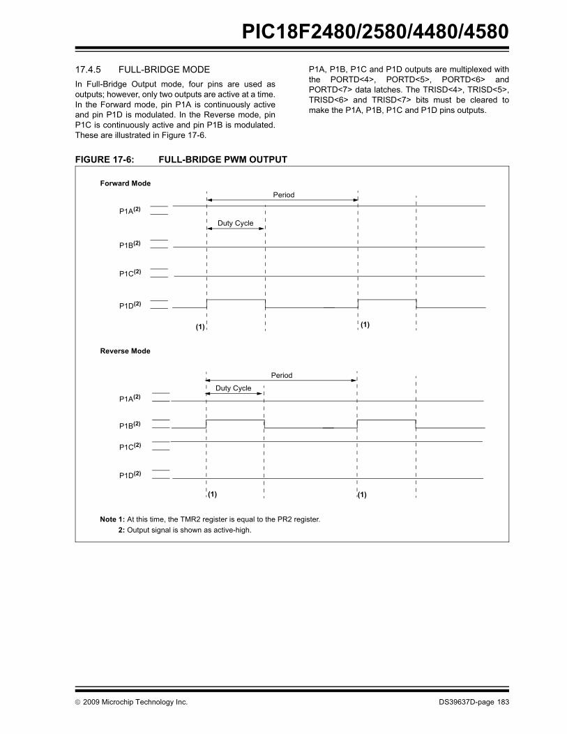
PIC18F2480/2580/4480/4580
17.4.5 FULL-BRIDGE MODEIn Full-Bridge Output mode, four pins are used asoutputs; however, only two outputs are active at a time.In the Forward mode, pin P1A is continuously activeand pin P1D is modulated. In the Reverse mode, pinP1C is continuously active and pin P1B is modulated.These are illustrated in Figure 17-6.P1A, P1B, P1C and P1D outputs are multiplexed withthe PORTD<4>, PORTD<5>, PORTD<6> andPORTD<7> data latches. The TRISD<4>, TRISD<5>,TRISD<6> and TRISD<7> bits must be cleared tomake the P1A, P1B, P1C and P1D pins outputs.
FIGURE 17-6: FULL-BRIDGE PWM OUTPUT
Period
Duty CycleP1A(2)
P1B(2)
P1C(2)
P1D(2)
Forward Mode
(1)
Period
Duty CycleP1A(2)
P1C(2)
P1D(2)
P1B(2)
Reverse Mode
(1)
(1)(1)
Note 1: At this time, the TMR2 register is equal to the PR2 register.Note 2: Output signal is shown as active-high.
© 2009 Microchip Technology Inc. DS39637D-page 183
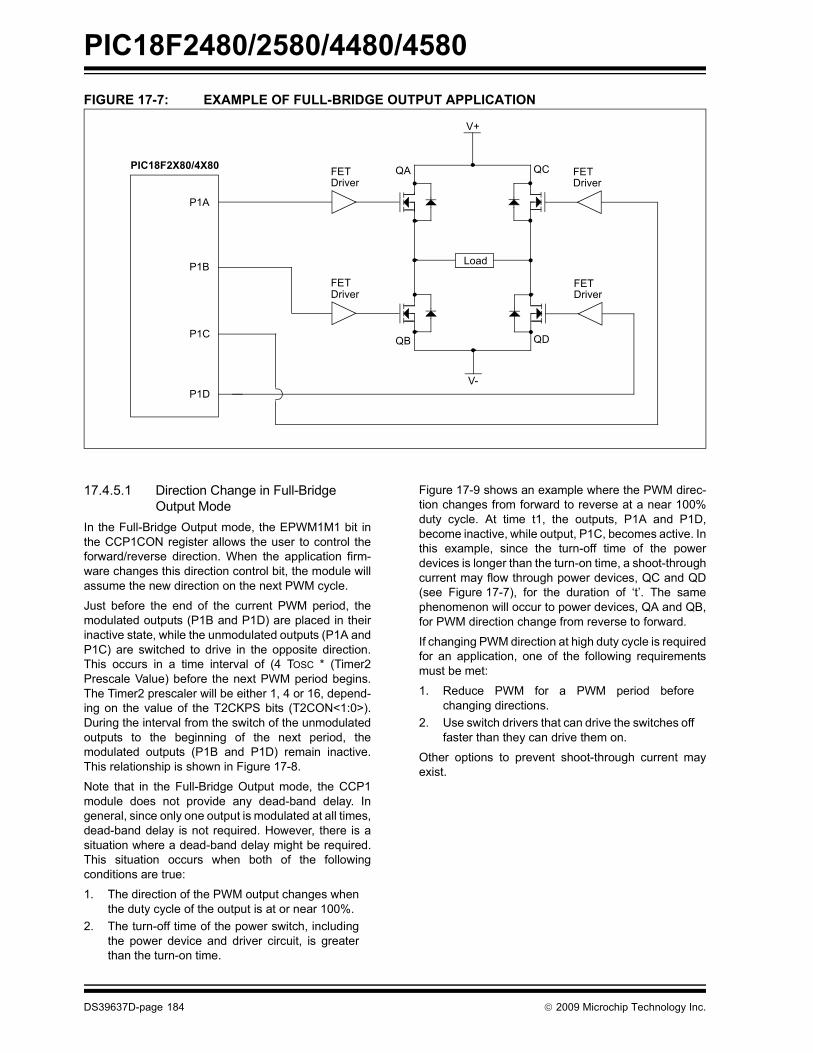
PIC18F2480/2580/4480/4580
FIGURE 17-7: EXAMPLE OF FULL-BRIDGE OUTPUT APPLICATION17.4.5.1 Direction Change in Full-Bridge Output Mode
In the Full-Bridge Output mode, the EPWM1M1 bit inthe CCP1CON register allows the user to control theforward/reverse direction. When the application firm-ware changes this direction control bit, the module willassume the new direction on the next PWM cycle.
Just before the end of the current PWM period, themodulated outputs (P1B and P1D) are placed in theirinactive state, while the unmodulated outputs (P1A andP1C) are switched to drive in the opposite direction.This occurs in a time interval of (4 TOSC * (Timer2Prescale Value) before the next PWM period begins.The Timer2 prescaler will be either 1, 4 or 16, depend-ing on the value of the T2CKPS bits (T2CON<1:0>).During the interval from the switch of the unmodulatedoutputs to the beginning of the next period, themodulated outputs (P1B and P1D) remain inactive.This relationship is shown in Figure 17-8.
Note that in the Full-Bridge Output mode, the CCP1module does not provide any dead-band delay. Ingeneral, since only one output is modulated at all times,dead-band delay is not required. However, there is asituation where a dead-band delay might be required.This situation occurs when both of the followingconditions are true:
1. The direction of the PWM output changes whenthe duty cycle of the output is at or near 100%.
2. The turn-off time of the power switch, includingthe power device and driver circuit, is greaterthan the turn-on time.
Figure 17-9 shows an example where the PWM direc-tion changes from forward to reverse at a near 100%duty cycle. At time t1, the outputs, P1A and P1D,become inactive, while output, P1C, becomes active. Inthis example, since the turn-off time of the powerdevices is longer than the turn-on time, a shoot-throughcurrent may flow through power devices, QC and QD(see Figure 17-7), for the duration of ‘t’. The samephenomenon will occur to power devices, QA and QB,for PWM direction change from reverse to forward.
If changing PWM direction at high duty cycle is requiredfor an application, one of the following requirementsmust be met:
1. Reduce PWM for a PWM period beforechanging directions.
2. Use switch drivers that can drive the switches offfaster than they can drive them on.
Other options to prevent shoot-through current mayexist.
P1A
P1C
FETDriver
FETDriver
V+
V-
Load
FETDriver
FETDriver
P1B
P1D
QA
QB QD
QCPIC18F2X80/4X80
DS39637D-page 184 © 2009 Microchip Technology Inc.

PIC18F2480/2580/4480/4580
FIGURE 17-8: PWM DIRECTION CHANGEFIGURE 17-9: PWM DIRECTION CHANGE AT NEAR 100% DUTY CYCLE
DC
Period(1)SIGNAL
Note 1: The direction bit in the CCP1 Control register (CCP1CON<7>) is written any time during the PWM cycle.2: When changing directions, the P1A and P1C signals switch before the end of the current PWM cycle at intervals
of 4 TOSC, 16 TOSC or 64 TOSC, depending on the Timer2 prescaler value. The modulated P1B and P1D signals are inactive at this time.
Period
(Note 2)
P1A (Active-High)
P1B (Active-High)
P1C (Active-High)
P1D (Active-High)
DC
Forward Period Reverse Period
P1A(1)
tON(2)
tOFF(3)
t = tOFF – tON(2,3)
P1B(1)
P1C(1)
P1D(1)
External Switch D(1)
PotentialShoot-Through
Current(1)
Note 1: All signals are shown as active-high.2: tON is the turn-on delay of power switch QC and its driver.3: tOFF is the turn-off delay of power switch QD and its driver.
External Switch C(1)
t1
DC
DC
© 2009 Microchip Technology Inc. DS39637D-page 185

PIC18F2480/2580/4480/4580
17.4.6 PROGRAMMABLE DEAD-BANDDELAY
In half-bridge applications where all power switches aremodulated at the PWM frequency at all times, the powerswitches normally require more time to turn off than toturn on. If both the upper and lower power switches areswitched at the same time (one turned on and the otherturned off), both switches may be on for a short period oftime until one switch completely turns off. During thisbrief interval, a very high current (shoot-through current)may flow through both power switches, shorting thebridge supply. To avoid this potentially destructiveshoot-through current from flowing during switching,turning on either of the power switches is normallydelayed to allow the other switch to completely turn off.
In the Half-Bridge Output mode, a digitally program-mable, dead-band delay is available to avoidshoot-through current from destroying the bridgepower switches. The delay occurs at the signal transi-tion from the non-active state to the active state (seeFigure 17-4 for illustration). Bits, PDC<6:0< of theECCP1DEL register (Register 17-2), set the delayperiod in terms of microcontroller instruction cycles(TCY or 4 TOSC). These bits are not available onPIC18F2X80 devices, as the standard CCP moduledoes not support half-bridge operation.
17.4.7 ENHANCED PWM AUTO-SHUTDOWNWhen the CCP1 is programmed for any of the EnhancedPWM modes, the active output pins may be configuredfor auto-shutdown. Auto-shutdown immediately placesthe Enhanced PWM output pins into a defined shutdownstate when a shutdown event occurs.
A shutdown event can be caused by either of thecomparator modules, a low level on theRB0/INT0/FLT0/AN10 pin, or any combination of thesethree sources. The comparators may be used to monitora voltage input proportional to a current being monitoredin the bridge circuit. If the voltage exceeds a threshold,the comparator switches state and triggers a shutdown.Alternatively, a digital signal on the INT0 pin can alsotrigger a shutdown. The auto-shutdown feature can bedisabled by not selecting any auto-shutdown sources.The auto-shutdown sources to be used are selectedusing the ECCPAS<2:0> bits (ECCP1AS<6:4>).
When a shutdown occurs, the output pins areasynchronously placed in their shutdown states,specified by the PSSAC<1:0> and PSS1BD<1:0> bits(ECCPAS<3:0>). Each pin pair (P1A/P1C and P1B/P1D)may be set to drive high, drive low or be tri-stated (notdriving). The ECCPASE bit (ECCP1AS<7>) is also set tohold the Enhanced PWM outputs in their shutdownstates.
The ECCPASE bit is set by hardware when a shutdownevent occurs. If automatic restarts are not enabled, theECCPASE bit is cleared by firmware when the cause ofthe shutdown clears. If automatic restarts are enabled,the ECCPASE bit is automatically cleared when thecause of the auto-shutdown has cleared.
If the ECCPASE bit is set when a PWM period begins,the PWM outputs remain in their shutdown state for thatentire PWM period. When the ECCPASE bit is cleared,the PWM outputs will return to normal operation at thebeginning of the next PWM period.
Note: Programmable dead-band delay is notimplemented in PIC18F2X80 devices withstandard CCP modules.
Note: Writing to the ECCPASE bit is disabledwhile a shutdown condition is active.
Note: If the dead-band delay value is increasedafter the dead-band time has elapsed, thatnew value takes effect immediately. Thishappens even if the PWM pulse is highand can appear to be a glitch. Dead-bandvalues must be changed during thedead-band time or before ECCP is active
DS39637D-page 186 © 2009 Microchip Technology Inc.

PIC18F2480/2580/4480/4580
REGISTER 17-2: ECCP1DEL: ECCP PWM DEAD-BAND DELAY REGISTER
R/W-0 R/W-0 R/W-0 R/W-0 R/W-0 R/W-0 R/W-0 R/W-0PRSEN PDC6(1) PDC5(1) PDC4(1) PDC3(1) PDC2(1) PDC1(1) PDC0(1)
bit 7 bit 0
Legend:R = Readable bit W = Writable bit U = Unimplemented bit, read as ‘0’-n = Value at POR ‘1’ = Bit is set ‘0’ = Bit is cleared x = Bit is unknown
bit 7 PRSEN: PWM Restart Enable bit1 = Upon auto-shutdown, the ECCPASE bit clears automatically once the shutdown event goes away;
the PWM restarts automatically0 = Upon auto-shutdown, ECCPASE must be cleared in software to restart the PWM
bit 6-0 PDC<6:0>: PWM Delay Count bits(1)
Delay time, in number of FOSC/4 (4 * TOSC) cycles, between the scheduled and actual time for a PWMsignal to transition to active.
Note 1: Reserved on PIC18F2X80 devices; maintain these bits clear.
REGISTER 17-3: ECCP1AS: ECCP AUTO-SHUTDOWN CONTROL REGISTER(1)
R/W-0 R/W-0 R/W-0 R/W-0 R/W-0 R/W-0 R/W-0 R/W-0ECCPASE ECCPAS2 ECCPAS1 ECCPAS0 PSSAC1 PSSAC0 PSSBD1(1) PSSBD0(1)
bit 7 bit 0
Legend:R = Readable bit W = Writable bit U = Unimplemented bit, read as ‘0’-n = Value at POR ‘1’ = Bit is set ‘0’ = Bit is cleared x = Bit is unknown
bit 7 ECCPASE: ECCP Auto-Shutdown Event Status bit1 = A shutdown event has occurred; ECCP outputs are in shutdown state0 = ECCP outputs are operating
bit 6-4 ECCPAS<2:0>: ECCP Auto-Shutdown Source Select bits111 = RB0 or Comparator 1 or Comparator 2110 = RB0 or Comparator 2101 = RB0 or Comparator 1100 = RB0011 = Either Comparator 1 or 2010 = Comparator 2 output001 = Comparator 1 output000 = Auto-shutdown is disabled
bit 3-2 PSSAC<1:0>: Pins, A and C, Shutdown State Control bits1x = Pins, A and C, tri-state (PIC18F4X80 devices)01 = Drive Pins, A and C, to ‘1’00 = Drive Pins, A and C, to ‘0’
bit 1-0 PSSBD<1:0>: Pins, B and D, Shutdown State Control bits(1)
1x = Pins, B and D, tri-state01 = Drive Pins, B and D, to ‘1’00 = Drive Pins, B and D, to ‘0’
Note 1: Reserved on PIC18F2X80 devices; maintain these bits clear.
© 2009 Microchip Technology Inc. DS39637D-page 187

PIC18F2480/2580/4480/4580
17.4.7.1 Auto-Shutdown and Auto-RestartThe auto-shutdown feature can be configured to allowautomatic restarts of the module following a shutdownevent. This is enabled by setting the PRSEN bit of theECCP1DEL register (ECCP1DEL<7>).In Shutdown mode with PRSEN = 1 (Figure 17-10), theECCPASE bit will remain set for as long as the causeof the shutdown continues. When the shutdown condi-tion clears, the ECCP1ASE bit is cleared. If PRSEN = 0(Figure 17-11), once a shutdown condition occurs, theECCPASE bit will remain set until it is cleared byfirmware. Once ECCPASE is cleared, the EnhancedPWM will resume at the beginning of the next PWMperiod.
Independent of the PRSEN bit setting, if theauto-shutdown source is one of the comparators, theshutdown condition is a level. The ECCPASE bitcannot be cleared as long as the cause of the shutdownpersists.
The Auto-Shutdown mode can be forced by writing a ‘1’to the ECCPASE bit.
17.4.8 START-UP CONSIDERATIONSWhen the ECCP module is used in the PWM mode, theapplication hardware must use the proper external pull-upand/or pull-down resistors on the PWM output pins. Whenthe microcontroller is released from Reset, all of the I/Opins are in the high-impedance state. The external circuitsmust keep the power switch devices in the off state untilthe microcontroller drives the I/O pins with the propersignal levels, or activates the PWM output(s).
The CCP1M<1:0> bits (ECCP1CON<1:0>) allow theuser to choose whether the PWM output signals areactive-high or active-low for each pair of PWM outputpins (P1A/P1C and P1B/P1D). The PWM outputpolarities must be selected before the PWM pins areconfigured as outputs. Changing the polarity configura-tion while the PWM pins are configured as outputs isnot recommended, since it may result in damage to theapplication circuits.
The P1A, P1B, P1C and P1D output latches may not bein the proper states when the PWM module is initialized.Enabling the PWM pins for output at the same time asthe ECCP module may cause damage to the applica-tion circuit. The ECCP module must be enabled in theproper output mode and complete a full PWM cyclebefore configuring the PWM pins as outputs. The com-pletion of a full PWM cycle is indicated by the TMR2IFbit being set as the second PWM period begins.
FIGURE 17-10: PWM AUTO-SHUTDOWN (PRSEN = 1, AUTO-RESTART ENABLED)
FIGURE 17-11: PWM AUTO-SHUTDOWN (PRSEN = 0, AUTO-RESTART DISABLED)
Note: Writing to the ECCPASE bit is disabledwhile a shutdown condition is active.
Shutdown
PWM
ECCPASE bit
Activity
Event
ShutdownEvent Occurs
ShutdownEvent Clears
PWMResumes
Normal PWM
Start ofPWM Period
PWM Period
Shutdown
PWM
ECCPASE bit
Activity
Event
ShutdownEvent Occurs
ShutdownEvent Clears
PWMResumes
Normal PWM
Start ofPWM Period
ECCPASECleared byFirmware
PWM Period
DS39637D-page 188 © 2009 Microchip Technology Inc.

PIC18F2480/2580/4480/4580
17.4.9 SETUP FOR PWM OPERATIONThe following steps should be taken when configuringthe ECCP module for PWM operation:1. Configure the PWM pins, P1A and P1B (andP1C and P1D, if used), as inputs by setting thecorresponding TRIS bits.
2. Set the PWM period by loading the PR2 register.3. Configure the ECCP1 module for the desired
PWM mode and configuration by loading theECCP1CON register with the appropriatevalues:• Select one of the available output
configurations and direction with the EPWM1M<1:0> bits.
• Select the polarities of the PWM output signals with the ECCP1M<3:0> bits.
4. Set the PWM duty cycle by loading theECCPR1L register and ECCP1CON<5:4> bits.
5. For Half-Bridge Output mode, set thedead-band delay by loading ECCP1DEL<6:0>with the appropriate value.
6. If auto-shutdown operation is required, load theECCP1AS register:• Select the auto-shutdown sources using the
ECCPAS<2:0> bits.• Select the shutdown states of the PWM
output pins using PSSAC<1:0> and PSSBD<1:0> bits.
• Set the ECCPASE bit (ECCP1AS<7>).• Configure the comparators using the CMCON
register.• Configure the comparator inputs as analog
inputs.
7. If auto-restart operation is required, set thePRSEN bit (ECCP1DEL<7>).
8. Configure and start TMR2:• Clear the TMR2 interrupt flag bit by clearing
the TMR2IF bit (PIR1<1>).• Set the TMR2 prescale value by loading the
T2CKPS bits (T2CON<1:0>).• Enable Timer2 by setting the TMR2ON bit
(T2CON<2>).9. Enable PWM outputs after a new PWM cycle
has started:• Wait until TMRn overflows (TMRnIF bit is set).• Enable the ECCP1/P1A, P1B, P1C and/or
P1D pin outputs by clearing the respective TRIS bits.
• Clear the ECCPASE bit (ECCP1AS<7>).
17.4.10 EFFECTS OF A RESETBoth Power-on Reset and subsequent Resets will forceall ports to Input mode and the CCP registers to theirReset states.
This forces the Enhanced CCP module to reset to astate compatible with the standard CCP module.
© 2009 Microchip Technology Inc. DS39637D-page 189

PIC18F2480/2580/4480/4580
TABLE 17-3: REGISTERS ASSOCIATED WITH ECCP1 MODULE AND TIMER1 TO TIMER3Name Bit 7 Bit 6 Bit 5 Bit 4 Bit 3 Bit 2 Bit 1 Bit 0Reset Values
on Page:
INTCON GIE/GIEH PEIE/GIEL TMR0IE INT0IE RBIE TMR0IF INT0IF RBIF 55
RCON IPEN SBOREN — RI TO PD POR BOR 56IPR1 PSPIP ADIP RCIP TXIP SSPIP CCP1IP TMR2IP TMR1IP 58PIR1 PSPIF ADIF RCIF TXIF SSPIF CCP1IF TMR2IF TMR1IF 58PIE1 PSPIE ADIE RCIE TXIE SSPIE CCP1IE TMR2IE TMR1IE 58IPR2 OSCFIP CMIP(3) — EEIP BCLIP HLVDIP TMR3IP ECCP1IP(3) 57PIR2 OSCFIF CMIF(3) — EEIF BCLIF HLVDIF TMR3IF ECCP1IF(3) 58PIE2 OSCFIE CMIE(3) — EEIE BCLIE HLVDIE TMR3IE ECCP1IE(3) 58TRISB PORTB Data Direction Register 58TRISC PORTC Data Direction Register 58TRISD(1) PORTD Data Direction Register 58TMR1L Holding Register for the Least Significant Byte of the 16-bit TMR1 Register 56TMR1H Holding Register for the Most Significant Byte of the 16-bit TMR1 Register 56
T1CON RD16 T1RUN T1CKPS1 T1CKPS0 T1OSCEN T1SYNC TMR1CS TMR1ON 56TMR2 Timer2 Module Register 56T2CON — T2OUTPS3 T2OUTPS2 T2OUTPS1 T2OUTPS0 TMR2ON T2CKPS1 T2CKPS0 56PR2 Timer2 Period Register 56TMR3L Holding Register for the Least Significant Byte of the 16-bit TMR3 Register 57TMR3H Holding Register for the Most Significant Byte of the 16-bit TMR3 Register 57
T3CON RD16 T3ECCP1(1) T3CKPS1 T3CKPS0 T3CCP1(1) T3SYNC TMR3CS TMR3ON 57ECCPR1L(2) Enhanced Capture/Compare/PWM Register 1 (LSB) 57ECCPR1H(2) Enhanced Capture/Compare/PWM Register 1 (MSB) 57ECCP1CON(2) EPWM1M1 EPWM1M0 EDC1B1 EDC1B0 ECCP1M3 ECCP1M2 ECCP1M1 ECCP1M0 57ECCP1AS(2) ECCPASE ECCPAS2 ECCPAS1 ECCPAS0 PSSAC1 PSSAC0 PSSBD1(2) PSSBD0(2) 57ECCP1DEL(2) PRSEN PDC6(2) PDC5(2) PDC4(2) PDC3(2) PDC2(2) PDC1(2) PDC0(2) 57Legend: — = unimplemented, read as ‘0’. Shaded cells are not used during ECCP operation.Note 1: These bits are available on PIC18F4X80 devices only.
2: These bits or registers are unimplemented in PIC18F2X80 devices; always maintain these bit clear.3: These bits are available on PIC18F4X80 and reserved on PIC18F2X80 devices.
DS39637D-page 190 © 2009 Microchip Technology Inc.

PIC18F2480/2580/4480/4580
18.0 MASTER SYNCHRONOUS SERIAL PORT (MSSP) MODULE
18.1 Master SSP (MSSP) Module Overview
The Master Synchronous Serial Port (MSSP) module isa serial interface, useful for communicating with otherperipheral or microcontroller devices. These peripheraldevices may be serial EEPROMs, shift registers,display drivers, A/D Converters, etc. The MSSPmodule can operate in one of two modes:
• Serial Peripheral Interface (SPI)• Inter-Integrated Circuit (I2C)
- Full Master mode- Slave mode (with general address call)
The I2C interface supports the following modes inhardware:
• Master mode• Multi-Master mode• Slave mode
18.2 Control RegistersThe MSSP module has three associated registers.These include a status register (SSPSTAT) and twocontrol registers (SSPCON1 and SSPCON2). The useof these registers and their individual configuration bitsdiffer significantly depending on whether the MSSPmodule is operated in SPI or I2C mode.
Additional details are provided under the individualsections.
18.3 SPI ModeThe SPI mode allows 8 bits of data to be synchronouslytransmitted and received simultaneously. All fourmodes of SPI are supported. To accomplishcommunication, typically three pins are used:
• Serial Data Out (SDO) – RC5/SDO • Serial Data In (SDI) – RC4/SDI/SDA• Serial Clock (SCK) – RC3/SCK/SCL
Additionally, a fourth pin may be used when in a Slavemode of operation:
• Slave Select (SS) – RA5/AN4/SS/HLVDIN
Figure 18-1 shows the block diagram of the MSSPmodule when operating in SPI mode.
FIGURE 18-1: MSSP BLOCK DIAGRAM (SPI MODE)
( )
Read Write
InternalData Bus
SSPSR reg
SSPM<3:0>
bit 0 ShiftClock
SS ControlEnable
EdgeSelect
Clock Select
TMR2 Output
TOSCPrescaler4, 16, 64
2EdgeSelect
2
4
Data to TX/RX in SSPSRTRIS bit
2SMP:CKE
SDO
SSPBUF reg
SDI
SS
SCK
© 2009 Microchip Technology Inc. DS39637D-page 191

PIC18F2480/2580/4480/4580
18.3.1 REGISTERSThe MSSP module has four registers for SPI modeoperation. These are:• MSSP Control Register 1 (SSPCON1)• MSSP Status Register (SSPSTAT)• Serial Receive/Transmit Buffer Register
(SSPBUF)• MSSP Shift Register (SSPSR) – Not directly
accessible
SSPCON1 and SSPSTAT are the control and statusregisters in SPI mode operation. The SSPCON1 regis-ter is readable and writable. The lower 6 bits of theSSPSTAT are read-only. The upper two bits of theSSPSTAT are read/write.
SSPSR is the shift register used for shifting data in orout. SSPBUF is the buffer register to which data bytesare written to or read from.
In receive operations, SSPSR and SSPBUF together,create a double-buffered receiver. When SSPSRreceives a complete byte, it is transferred to SSPBUFand the SSPIF interrupt is set.
During transmission, the SSPBUF is not double-buffered. A write to SSPBUF will write to both SSPBUFand SSPSR.
REGISTER 18-1: SSPSTAT: MSSP STATUS REGISTER (SPI MODE)
R/W-0 R/W-0 R-0 R-0 R-0 R-0 R-0 R-0
SMP CKE D/A P S R/W UA BFbit 7 bit 0
Legend:R = Readable bit W = Writable bit U = Unimplemented bit, read as ‘0’-n = Value at POR ‘1’ = Bit is set ‘0’ = Bit is cleared x = Bit is unknown
bit 7 SMP: Sample bitSPI Master mode:1 = Input data sampled at end of data output time0 = Input data sampled at middle of data output timeSPI Slave mode:SMP must be cleared when SPI is used in Slave mode.
bit 6 CKE: SPI Clock Select bit1 = Transmit occurs on transition from active to Idle clock state0 = Transmit occurs on transition from Idle to active clock statePolarity of clock state is set by the CKP bit (SSPCON1<4>).
bit 5 D/A: Data/Address bit Used in I2C mode only.
bit 4 P: Stop bit Used in I2C mode only. This bit is cleared when the MSSP module is disabled, SSPEN is cleared.
bit 3 S: Start bitUsed in I2C mode only.
bit 2 R/W: Read/Write Information bitUsed in I2C mode only.
bit 1 UA: Update Address bitUsed in I2C mode only.
bit 0 BF: Buffer Full Status bit (Receive mode only)1 = Receive complete, SSPBUF is full 0 = Receive not complete, SSPBUF is empty
DS39637D-page 192 © 2009 Microchip Technology Inc.

PIC18F2480/2580/4480/4580
REGISTER 18-2: SSPCON1: MSSP CONTROL REGISTER 1 (SPI MODE)R/W-0 R/W-0 R/W-0 R/W-0 R/W-0 R/W-0 R/W-0 R/W-0WCOL SSPOV(1) SSPEN(2) CKP SSPM3(3) SSPM2(3) SSPM1(3) SSPM0(3)
bit 7 bit 0
Legend:R = Readable bit W = Writable bit U = Unimplemented bit, read as ‘0’-n = Value at POR ‘1’ = Bit is set ‘0’ = Bit is cleared x = Bit is unknown
bit 7 WCOL: Write Collision Detect bit (Transmit mode only)1 = The SSPBUF register is written while it is still transmitting the previous word
(must be cleared in software) 0 = No collision
bit 6 SSPOV: Receive Overflow Indicator bit(1) SPI Slave mode: 1 = A new byte is received while the SSPBUF register is still holding the previous data. In case of over-
flow, the data in SSPSR is lost. Overflow can only occur in Slave mode. The user must read theSSPBUF, even if only transmitting data, to avoid setting overflow (must be cleared in software).
0 = No overflowbit 5 SSPEN: Master Synchronous Serial Port Enable bit(2)
1 = Enables serial port and configures SCK, SDO, SDI and SS as serial port pins(2) 0 = Disables serial port and configures these pins as I/O port pins(2)
bit 4 CKP: Clock Polarity Select bit 1 = Idle state for clock is a high level 0 = Idle state for clock is a low level
bit 3-0 SSPM3:SSPM0: Master Synchronous Serial Port Mode Select bits(3)
0101 = SPI Slave mode, clock = SCK pin, SS pin control disabled, SS can be used as I/O pin0100 = SPI Slave mode, clock = SCK pin, SS pin control enabled0011 = SPI Master mode, clock = TMR2 output/20010 = SPI Master mode, clock = FOSC/640001 = SPI Master mode, clock = FOSC/160000 = SPI Master mode, clock = FOSC/4
Note 1: In Master mode, the overflow bit is not set since each new reception (and transmission) is initiated by writing to the SSPBUF register.
2: When enabled, these pins must be properly configured as input or output.3: Bit combinations not specifically listed here are either reserved or implemented in I2C™ mode only.
© 2009 Microchip Technology Inc. DS39637D-page 193

PIC18F2480/2580/4480/4580
18.3.2 OPERATIONWhen initializing the SPI, several options need to bespecified. This is done by programming the appropriatecontrol bits (SSPCON1<5:0> and SSPSTAT<7:6>).These control bits allow the following to be specified:• Master mode (SCK is the clock output)• Slave mode (SCK is the clock input)• Clock Polarity (Idle state of SCK)• Data Input Sample Phase (middle or end of data
output time)• Clock Edge (output data on rising/falling edge of
SCK)• Clock Rate (Master mode only)• Slave Select mode (Slave mode only)
The MSSP consists of a Transmit/Receive Shift regis-ter (SSPSR) and a Buffer register (SSPBUF). TheSSPSR shifts the data in and out of the device, MSbfirst. The SSPBUF holds the data that was written to theSSPSR until the received data is ready. Once the 8 bitsof data have been received, that byte is moved to theSSPBUF register. Then, the Buffer Full detect bit, BF(SSPSTAT<0>), and the interrupt flag bit, SSPIF, areset. This double-buffering of the received data(SSPBUF) allows the next byte to start reception beforereading the data that was just received. Any write to theSSPBUF register during transmission/reception of datawill be ignored and the write collision detect bit, WCOL(SSPCON1<7>), will be set. User software must clear
the WCOL bit so that it can be determined if the follow-ing write(s) to the SSPBUF register completedsuccessfully.
When the application software is expecting to receivevalid data, the SSPBUF should be read before the nextbyte of data to transfer is written to the SSPBUF. TheBuffer Full bit, BF (SSPSTAT<0>), indicates whenSSPBUF has been loaded with the received data(transmission is complete). When the SSPBUF is read,the BF bit is cleared. This data may be irrelevant if theSPI is only a transmitter. Generally, the MSSP interruptis used to determine when the transmission/receptionhas completed. The SSPBUF must be read and/orwritten. If the interrupt method is not going to be used,then software polling can be done to ensure that a writecollision does not occur. Example 18-1 shows theloading of the SSPBUF (SSPSR) for data transmission.
The SSPSR is not directly readable or writable and canonly be accessed by addressing the SSPBUF register.Additionally, the MSSP Status register (SSPSTAT)indicates the various status conditions.
EXAMPLE 18-1: LOADING THE SSPBUF (SSPSR) REGISTER
Note: The SSPBUF register cannot be used withread-modify-write instructions such asBCF, BTFSC and COMF, etc.
Note: To avoid lost data in Master mode, a read ofthe SSPBUF must be performed to clear theBuffer Full (BF) detect bit (SSPSTAT<0>)between each transmission.
LOOP BTFSS SSPSTAT, BF ;Has data been received (transmit complete)? BRA LOOP ;No MOVF SSPBUF, W ;WREG reg = contents of SSPBUF
MOVWF RXDATA ;Save in user RAM, if data is meaningful
MOVF TXDATA, W ;W reg = contents of TXDATA MOVWF SSPBUF ;New data to xmit
DS39637D-page 194 © 2009 Microchip Technology Inc.

PIC18F2480/2580/4480/4580
18.3.3 ENABLING SPI I/OTo enable the serial port, MSSP Enable bit, SSPEN(SSPCON1<5>), must be set. To reset or reconfigureSPI mode, clear the SSPEN bit, reinitialize theSSPCON registers and then set the SSPEN bit. Thisconfigures the SDI, SDO, SCK and SS pins as serialport pins. For the pins to behave as the serial port func-tion, some must have their data direction bits (in theTRIS register) appropriately programmed as follows:• SDI is automatically controlled by the SPI module • SDO must have TRISC<5> bit cleared• SCK (Master mode) must have TRISC<3> bit
cleared• SCK (Slave mode) must have TRISC<3> bit set • SS must have TRISF<7> bit set
Any serial port function that is not desired may beoverridden by programming the corresponding DataDirection (TRIS) register to the opposite value.
18.3.4 TYPICAL CONNECTIONFigure 18-2 shows a typical connection between twomicrocontrollers. The master controller (Processor 1)initiates the data transfer by sending the SCK signal.Data is shifted out of both shift registers on their pro-grammed clock edge and latched on the opposite edgeof the clock. Both processors should be programmed tothe same Clock Polarity (CKP), then both controllerswould send and receive data at the same time.Whether the data is meaningful (or dummy data)depends on the application software. This leads tothree scenarios for data transmission:
• Master sends data – Slave sends dummy data• Master sends data – Slave sends data• Master sends dummy data – Slave sends data
FIGURE 18-2: SPI MASTER/SLAVE CONNECTION
Note: When the module is enabled and inMaster mode (CKE, SSPSTAT<6> = 1), asmall glitch of approximately half a TCYmay be seen on the SCK pin. To resolvethis, keep the SCK pin as an input whilesetting SPEN. Then, configure the SCKpin as an output (TRISC<3> = 0).
Serial Input Buffer(SSPBUF)
Shift Register(SSPSR)
MSb LSb
SDO
SDI
PROCESSOR 1
SCK
SPI Master SSPM<3:0> = 00xxb
Serial Input Buffer(SSPBUF)
Shift Register(SSPSR)
LSbMSb
SDI
SDO
PROCESSOR 2
SCK
SPI Slave SSPM<3:0> = 010xb
Serial Clock
© 2009 Microchip Technology Inc. DS39637D-page 195

PIC18F2480/2580/4480/4580
18.3.5 MASTER MODEThe master can initiate the data transfer at any timebecause it controls the SCK. The master determineswhen the slave (Processor 2, Figure 18-2) is tobroadcast data by the software protocol.In Master mode, the data is transmitted/received assoon as the SSPBUF register is written to. If the SPI isonly going to receive, the SDO output could be dis-abled (programmed as an input). The SSPSR registerwill continue to shift in the signal present on the SDI pinat the programmed clock rate. As each byte isreceived, it will be loaded into the SSPBUF register asif a normal received byte (interrupts and status bitsappropriately set). This could be useful in receiverapplications as a “Line Activity Monitor” mode.
The clock polarity is selected by appropriatelyprogramming the CKP bit (SSPCON1<4>). This then,would give waveforms for SPI communication asshown in Figure 18-3, Figure 18-5 and Figure 18-6,where the MSB is transmitted first. In Master mode, theSPI clock rate (bit rate) is user-programmable to be oneof the following:
• FOSC/4 (or TCY)• FOSC/16 (or 4 • TCY)• FOSC/64 (or 16 • TCY)• Timer2 output/2
This allows a maximum data rate (at 40 MHz) of10.00 Mbps.
Figure 18-3 shows the waveforms for Master mode.When the CKE bit is set, the SDO data is valid beforethere is a clock edge on SCK. The change of the inputsample is shown based on the state of the SMP bit. Thetime when the SSPBUF is loaded with the receiveddata is shown.
FIGURE 18-3: SPI MODE WAVEFORM (MASTER MODE)
SCK(CKP = 0
SCK(CKP = 1
SCK(CKP = 0
SCK(CKP = 1
4 ClockModes
InputSample
InputSample
SDI
bit 7 bit 0
SDO bit 7 bit 6 bit 5 bit 4 bit 3 bit 2 bit 1 bit 0
bit 7SDI
SSPIF(SMP = 1)
(SMP = 0)
(SMP = 1)
CKE = 1)
CKE = 0)
CKE = 1)
CKE = 0)
(SMP = 0)
Write toSSPBUF
SSPSR toSSPBUF
SDO bit 7 bit 6 bit 5 bit 4 bit 3 bit 2 bit 1 bit 0
(CKE = 0)
(CKE = 1)
Next Q4 Cycleafter Q2↓
bit 0
DS39637D-page 196 © 2009 Microchip Technology Inc.

PIC18F2480/2580/4480/4580
18.3.6 SLAVE MODEIn Slave mode, the data is transmitted and received asthe external clock pulses appear on SCK. When thelast bit is latched, the SSPIF interrupt flag bit is set.Before enabling the module in SPI Slave mode, theclock line must match the proper Idle state. The clockline can be observed by reading the SCK pin. The Idlestate is determined by the CKP bit (SSPCON1<4>).
While in Slave mode, the external clock is supplied bythe external clock source on the SCK pin. This externalclock must meet the minimum high and low times asspecified in the electrical specifications.
While in Sleep mode, the slave can transmit/receivedata. When a byte is received, the device will wake-upfrom Sleep.
18.3.7 SLAVE SELECT SYNCHRONIZATION
The SS pin allows a Synchronous Slave mode. TheSPI must be in Slave mode with SS pin control enabled(SSPCON1<3:0> = 04h). The pin must not be drivenlow for the SS pin to function as an input. The data latch
must be high. When the SS pin is low, transmission andreception are enabled and the SDO pin is driven. Whenthe SS pin goes high, the SDO pin is no longer driveneven if in the middle of a transmitted byte and becomesa floating output. External pull-up/pull-down resistorsmay be desirable depending on the application.
When the SPI module resets, the bit counter is forcedto ‘0’. This can be done by either forcing the SS pin toa high level or clearing the SSPEN bit.
To emulate two-wire communication, the SDO pin canbe connected to the SDI pin. When the SPI needs tooperate as a receiver, the SDO pin can be configuredas an input. This disables transmissions from the SDO.The SDI can always be left as an input (SDI function)since it cannot create a bus conflict.
FIGURE 18-4: SLAVE SYNCHRONIZATION WAVEFORM
Note 1: When the SPI is in Slave mode with SS pincontrol enabled (SSPCON<3:0> = 0100),the SPI module will reset if the SS pin is setto VDD.
2: If the SPI is used in Slave mode with CKEset, then the SS pin control must beenabled.
SCK(CKP = 1
SCK(CKP = 0
InputSample
SDI
bit 7
SDO bit 7 bit 6 bit 7
SSPIFInterrupt
(SMP = 0)
CKE = 0)
CKE = 0)
(SMP = 0)
Write toSSPBUF
SSPSR toSSPBUF
SS
Flag
bit 0
bit 7bit 0
Next Q4 Cycleafter Q2↓
© 2009 Microchip Technology Inc. DS39637D-page 197

PIC18F2480/2580/4480/4580
FIGURE 18-5: SPI MODE WAVEFORM (SLAVE MODE WITH CKE = 0)FIGURE 18-6: SPI MODE WAVEFORM (SLAVE MODE WITH CKE = 1)
SCK(CKP = 1
SCK(CKP = 0
InputSample
SDIbit 7
SDO bit 7 bit 6 bit 5 bit 4 bit 3 bit 2 bit 1 bit 0
SSPIFInterrupt
(SMP = 0)
CKE = 0)
CKE = 0)
(SMP = 0)
Write toSSPBUF
SSPSR toSSPBUF
SS
Flag
Optional
Next Q4 Cycleafter Q2↓
bit 0
SCK(CKP = 1
SCK(CKP = 0
InputSample
SDI
bit 7 bit 0
SDO bit 7 bit 6 bit 5 bit 4 bit 3 bit 2 bit 1 bit 0
SSPIFInterrupt
(SMP = 0)
CKE = 1)
CKE = 1)
(SMP = 0)
Write toSSPBUF
SSPSR toSSPBUF
SS
Flag
Not Optional
Next Q4 Cycleafter Q2↓
DS39637D-page 198 © 2009 Microchip Technology Inc.

PIC18F2480/2580/4480/4580
18.3.8 OPERATION IN POWER-MANAGEDMODES
In SPI Master mode, module clocks may be operatingat a different speed than when in full-power mode; inthe case of the Sleep mode, all clocks are halted.
In most power-managed modes, a clock is provided tothe peripherals. That clock should be from the primaryclock source, the secondary clock (Timer1 oscillator at32.768 kHz) or the INTOSC source. See Section 3.7“Clock Sources and Oscillator Switching” foradditional information.
In most cases, the speed that the master clocks SPIdata is not important; however, this should beevaluated for each system.
If MSSP interrupts are enabled, they can wake the con-troller from Sleep mode, or one of the Idle modes, whenthe master completes sending data. If an exit fromSleep or Idle mode is not desired, MSSP interruptsshould be disabled.
If the Sleep mode is selected, all module clocks arehalted and the transmission/reception will remain inthat state until the device wakes. After the devicereturns to Run mode, the module will resumetransmitting and receiving data.
In SPI Slave mode, the SPI Transmit/Receive Shiftregister operates asynchronously to the device. Thisallows the device to be placed in any power-managedmode and data to be shifted into the SPI Transmit/Receive Shift register. When all 8 bits have beenreceived, the MSSP interrupt flag bit will be set and ifenabled, will wake the device.
18.3.9 EFFECTS OF A RESETA Reset disables the MSSP module and terminates thecurrent transfer.
18.3.10 BUS MODE COMPATIBILITYTable 18-1 shows the compatibility between thestandard SPI modes and the states of the CKP andCKE control bits.
TABLE 18-1: SPI BUS MODES
There is also a SMP bit which controls when the data issampled.
TABLE 18-2: REGISTERS ASSOCIATED WITH SPI OPERATION
Standard SPI Mode Terminology
Control Bits State
CKP CKE
0, 0 0 1
0, 1 0 0
1, 0 1 1
1, 1 1 0
Name Bit 7 Bit 6 Bit 5 Bit 4 Bit 3 Bit 2 Bit 1 Bit 0Reset Values
on Page:
INTCON GIE/GIEH PEIE/GIEL TMR0IE INT0IE RBIE TMR0IF INT0IF RBIF 55PIR1 PSPIF(1) ADIF RCIF TXIF SSPIF CCP1IF TMR2IF TMR1IF 58PIE1 PSPIE(1) ADIE RCIE TXIE SSPIE CCP1IE TMR2IE TMR1IE 58IPR1 PSPIP(1) ADIP RCIP TXIP SSPIP CCP1IP TMR2IP TMR1IP 58TRISA PORTA Data Direction Register 58TRISC PORTC Data Direction Register 58SSPBUF Synchronous Serial Port Receive Buffer/Transmit Register 56SSPCON1 WCOL SSPOV SSPEN CKP SSPM3 SSPM2 SSPM1 SSPM0 56
SSPSTAT SMP CKE D/A P S R/W UA BF 56Legend: — = unimplemented, read as ‘0’. Shaded cells are not used by the MSSP in SPI mode.Note 1: These bits are unimplemented in PIC18F2X80 devices; always maintain these bits clear.
© 2009 Microchip Technology Inc. DS39637D-page 199

PIC18F2480/2580/4480/4580
18.4 I2C ModeThe MSSP module in I2C mode fully implements allmaster and slave functions (including general callsupport) and provides interrupts on Start and Stop bitsin hardware to determine a free bus (multi-masterfunction). The MSSP module implements the standardmode specifications, as well as 7-bit and 10-bitaddressing.Two pins are used for data transfer:
• Serial Clock (SCL) – RC3/SCK/SCL • Serial Data (SDA) – RC4/SDI/SDA
The user must configure these pins as inputs or outputsthrough the TRISC<4:3> bits.
FIGURE 18-7: MSSP BLOCK DIAGRAM (I2C™ MODE)
18.4.1 REGISTERSThe MSSP module has six registers for I2C operation.These are:
• MSSP Control Register 1 (SSPCON1)• MSSP Control Register 2 (SSPCON2)• MSSP Status Register (SSPSTAT)• Serial Receive/Transmit Buffer Register
(SSPBUF)• MSSP Shift Register (SSPSR) – Not directly
accessible• MSSP Address Register (SSPADD)
SSPCON1, SSPCON2 and SSPSTAT are the controland status registers in I2C mode operation. TheSSPCON1 and SSPCON2 registers are readable andwritable. The lower 6 bits of the SSPSTAT are read-only.The upper two bits of the SSPSTAT are read/write.
SSPSR is the shift register used for shifting data in orout. SSPBUF is the buffer register to which data bytesare written to or read from.
SSPADD register holds the slave device addresswhen the MSSP is configured in I2C Slave mode.When the MSSP is configured in Master mode, thelower seven bits of SSPADD act as the Baud RateGenerator reload value.
In receive operations, SSPSR and SSPBUF together,create a double-buffered receiver. When SSPSRreceives a complete byte, it is transferred to SSPBUFand the SSPIF interrupt is set.
During transmission, the SSPBUF is not double-buffered. A write to SSPBUF will write to both SSPBUFand SSPSR.
Read Write
SSPSR reg
Match Detect
SSPADD reg
Start andStop bit Detect
SSPBUF reg
InternalData Bus
Addr Match
Set, ResetS, P bits
(SSPSTAT reg)
SCL
SDA
ShiftClock
MSb LSb
DS39637D-page 200 © 2009 Microchip Technology Inc.

PIC18F2480/2580/4480/4580
REGISTER 18-3: SSPSTAT: MSSP STATUS REGISTER (I2C™ MODE)R/W-0 R/W-0 R-0 R-0 R-0 R-0 R-0 R-0
SMP CKE D/A P(1) S(1) R/W(2,3) UA BFbit 7 bit 0
Legend:R = Readable bit W = Writable bit U = Unimplemented bit, read as ‘0’-n = Value at POR ‘1’ = Bit is set ‘0’ = Bit is cleared x = Bit is unknown
bit 7 SMP: Slew Rate Control bitIn Master or Slave mode:1 = Slew rate control disabled for Standard Speed mode (100 kHz and 1 MHz) 0 = Slew rate control enabled for High-Speed mode (400 kHz)
bit 6 CKE: SMBus Select bitIn Master or Slave mode:1 = Enable SMBus specific inputs 0 = Disable SMBus specific inputs
bit 5 D/A: Data/Address bit In Master mode:Reserved.In Slave mode:1 = Indicates that the last byte received or transmitted was data0 = Indicates that the last byte received or transmitted was address
bit 4 P: Stop bit(1) 1 = Indicates that a Stop bit has been detected last0 = Stop bit was not detected last
bit 3 S: Start bit(1)
1 = Indicates that a Start bit has been detected last0 = Start bit was not detected last
bit 2 R/W: Read/Write Information bit (I2C mode only)(2,3)
In Slave mode:1 = Read0 = WriteIn Master mode:1 = Transmit is in progress0 = Transmit is not in progress
bit 1 UA: Update Address bit (10-Bit Slave mode only)1 = Indicates that the user needs to update the address in the SSPADD register 0 = Address does not need to be updated
bit 0 BF: Buffer Full Status bitIn Receive mode: 1 = Receive complete, SSPBUF is full 0 = Receive is not complete, SSPBUF is emptyIn Transmit mode:1 = Data transmit in progress (does not include the ACK and Stop bits), SSPBUF is full0 = Data transmit complete (does not include the ACK and Stop bits), SSPBUF is empty
Note 1: This bit is cleared on Reset and when SSPEN is cleared.2: This bit holds the R/W bit information following the last address match. This bit is only valid from the
address match to the next Start bit, Stop bit or not ACK bit.3: ORing this bit with SEN, RSEN, PEN, RCEN or ACKEN will indicate if the MSSP is in Idle mode.
© 2009 Microchip Technology Inc. DS39637D-page 201

PIC18F2480/2580/4480/4580
REGISTER 18-4: SSPCON1: MSSP CONTROL REGISTER 1 (I2C™ MODE)R/W-0 R/W-0 R/W-0 R/W-0 R/W-0 R/W-0 R/W-0 R/W-0WCOL SSPOV SSPEN(1) CKP SSPM3(2) SSPM2(2) SSPM1(2) SSPM0(2)
bit 7 bit 0
Legend:R = Readable bit W = Writable bit U = Unimplemented bit, read as ‘0’-n = Value at POR ‘1’ = Bit is set ‘0’ = Bit is cleared x = Bit is unknown
bit 7 WCOL: Write Collision Detect bitIn Master Transmit mode:1 = A write to the SSPBUF register was attempted while the I2C conditions were not valid for a
transmission to be started (must be cleared in software)0 = No collisionIn Slave Transmit mode:1 = The SSPBUF register is written while it is still transmitting the previous word (must be cleared in
software)0 = No collision In Receive mode (Master or Slave modes):This is a “don’t care” bit.
bit 6 SSPOV: Receive Overflow Indicator bit In Receive mode:1 = A byte is received while the SSPBUF register is still holding the previous byte (must be cleared in
software)0 = No overflowIn Transmit mode: This is a “don’t care” bit in Transmit mode.
bit 5 SSPEN: Master Synchronous Serial Port Enable bit(1) 1 = Enables the serial port and configures the SDA and SCL pins as the serial port pins0 = Disables serial port and configures these pins as I/O port pins
bit 4 CKP: SCK Release Control bit In Slave mode: 1 = Releases clock 0 = Holds clock low (clock stretch), used to ensure data setup timeIn Master mode: Unused in this mode.
bit 3-0 SSPM<3:0>: Master Synchronous Serial Port Mode Select bits(2)
1111 = I2C Slave mode, 10-bit address with Start and Stop bit interrupts enabled1110 = I2C Slave mode, 7-bit address with Start and Stop bit interrupts enabled1011 = I2C Firmware Controlled Master mode (slave Idle)1000 = I2C Master mode, clock = FOSC/(4 * (SSPADD + 1)) 0111 = I2C Slave mode, 10-bit address0110 = I2C Slave mode, 7-bit address
Note 1: When enabled, the SDA and SCL pins must be properly configured as input or output.2: Bit combinations not specifically listed here are either reserved or implemented in SPI mode only.
DS39637D-page 202 © 2009 Microchip Technology Inc.

PIC18F2480/2580/4480/4580
REGISTER 18-5: SSPCON2: MSSP CONTROL REGISTER 2 (I2C™ MODE)R/W-0 R/W-0 R/W-0 R/W-0 R/W-0 R/W-0 R/W-0 R/W-0GCEN ACKSTAT ACKDT(1) ACKEN(2) RCEN(2) PEN(2) RSEN(2) SEN(2)
bit 7 bit 0
Legend:R = Readable bit W = Writable bit U = Unimplemented bit, read as ‘0’-n = Value at POR ‘1’ = Bit is set ‘0’ = Bit is cleared x = Bit is unknown
bit 7 GCEN: General Call Enable bit (Slave mode only) 1 = Enables interrupt when a general call address (0000h) is received in the SSPSR 0 = General call address disabled
bit 6 ACKSTAT: Acknowledge Status bit (Master Transmit mode only)1 = Acknowledge was not received from slave 0 = Acknowledge was received from slave
bit 5 ACKDT: Acknowledge Data bit (Master Receive mode only)(1)
1 = Not Acknowledge 0 = Acknowledge
bit 4 ACKEN: Acknowledge Sequence Enable bit (Master Receive mode only)(2)
1 = Initiates Acknowledge sequence on SDA and SCL pins and transmits the ACKDT data bit.Automatically cleared by hardware.
0 = Acknowledge sequence Idle bit 3 RCEN: Receive Enable bit (Master mode only)(2)
1 = Enables Receive mode for I2C 0 = Receive Idle
bit 2 PEN: Stop Condition Enable bit (Master mode only)(2)
1 = Initiates Stop condition on SDA and SCL pins. Automatically cleared by hardware. 0 = Stop condition Idle
bit 1 RSEN: Repeated Start Condition Enable bit (Master mode only(2)
1 = Initiates Repeated Start condition on SDA and SCL pins. Automatically cleared by hardware. 0 = Repeated Start condition Idle
bit 0 SEN: Start Condition Enable/Stretch Enable bit(2)
In Master mode:1 = Initiates Start condition on SDA and SCL pins. Automatically cleared by hardware. 0 = Start condition IdleIn Slave mode:1 = Clock stretching is enabled for both slave transmit and slave receive (stretch enabled)0 = Clock stretching is disabled
Note 1: Value that will be transmitted when the user initiates an Acknowledge sequence at the end of a receive.2: For bits, ACKEN, RCEN, PEN, RSEN, SEN: If the I2C module is not in the Idle mode, these bits may not
be set (no spooling) and the SSPBUF may not be written (or writes to the SSPBUF are disabled).
© 2009 Microchip Technology Inc. DS39637D-page 203

PIC18F2480/2580/4480/4580
18.4.2 OPERATIONThe MSSP module functions are enabled by setting theMSSP Enable bit, SSPEN (SSPCON<5>).The SSPCON1 register allows control of the I2Coperation. Four mode selection bits (SSPCON<3:0>)allow one of the following I2C modes to be selected:
• I2C Master mode, clock = (FOSC/4) x (SSPADD + 1)• I2C Slave mode (7-bit address)• I2C Slave mode (10-bit address)• I2C Slave mode (7-bit address) with Start and
Stop bit interrupts enabled• I2C Slave mode (10-bit address) with Start and
Stop bit interrupts enabled• I2C Firmware Controlled Master mode, slave is
Idle
Selection of any I2C mode with the SSPEN bit set,forces the SCL and SDA pins to be open-drain,provided these pins are programmed to inputs bysetting the appropriate TRISC bits. To ensure properoperation of the module, pull-up resistors must beprovided externally to the SCL and SDA pins.
18.4.3 SLAVE MODEIn Slave mode, the SCL and SDA pins must be config-ured as inputs (TRISC<4:3> set). The MSSP modulewill override the input state with the output data whenrequired (slave-transmitter).
The I2C Slave mode hardware will always generate aninterrupt on an address match. Through the modeselect bits, the user can also choose to interrupt onStart and Stop bits
When an address is matched, or the data transfer afteran address match is received, the hardware automati-cally will generate the Acknowledge (ACK) pulse andload the SSPBUF register with the received valuecurrently in the SSPSR register.
Any combination of the following conditions will causethe MSSP module not to give this ACK pulse:
• The Buffer Full bit, BF (SSPSTAT<0>), was set before the transfer was received.
• The overflow bit, SSPOV (SSPCON<6>), was set before the transfer was received.
In this case, the SSPSR register value is not loadedinto the SSPBUF, but bit, SSPIF (PIR1<3>), is set. TheBF bit is cleared by reading the SSPBUF register, whilebit SSPOV is cleared through software.
The SCL clock input must have a minimum high andlow for proper operation. The high and low times of theI2C specification, as well as the requirement of theMSSP module, are shown in timing parameter 100 andparameter 101.
18.4.3.1 AddressingOnce the MSSP module has been enabled, it waits fora Start condition to occur. Following the Start condition,the 8-bits are shifted into the SSPSR register. Allincoming bits are sampled with the rising edge of theclock (SCL) line. The value of register, SSPSR<7:1>, iscompared to the value of the SSPADD register. Theaddress is compared on the falling edge of the eighthclock (SCL) pulse. If the addresses match and the BFand SSPOV bits are clear, the following events occur:
1. The SSPSR register value is loaded into theSSPBUF register.
2. The Buffer Full bit, BF, is set.3. An ACK pulse is generated.4. MSSP Interrupt Flag bit, SSPIF (PIR1<3>), is
set (interrupt is generated, if enabled) on thefalling edge of the ninth SCL pulse.
In 10-Bit Addressing mode, two address bytes need tobe received by the slave. The five Most Significant bits(MSbs) of the first address byte specify if this is a 10-bitaddress. Bit, R/W (SSPSTAT<2>), must specify a writeso the slave device will receive the second addressbyte. For a 10-bit address, the first byte would equal‘11110 A9 A8 0’, where ‘A9’ and ‘A8’ are the twoMSbs of the address. The sequence of events for10-bit addressing is as follows, with steps 7 through9 for the slave-transmitter:
1. Receive first (high) byte of address (bits, SSPIF,BF and UA (SSPSTAT<1>), are set).
2. Update the SSPADD register with second (low)byte of address (clears bit, UA, and releases theSCL line).
3. Read the SSPBUF register (clears bit, BF) andclear flag bit, SSPIF.
4. Receive second (low) byte of address (bits,SSPIF, BF and UA, are set).
5. Update the SSPADD register with the first (high)byte of address. If match releases SCL line, thiswill clear bit, UA.
6. Read the SSPBUF register (clears bit BF) andclear flag bit, SSPIF.
7. Receive Repeated Start condition.8. Receive first (high) byte of address (bits, SSPIF
and BF, are set).9. Read the SSPBUF register (clears bit, BF) and
clear flag bit, SSPIF.
DS39637D-page 204 © 2009 Microchip Technology Inc.

PIC18F2480/2580/4480/4580
18.4.3.2 ReceptionWhen the R/W bit of the address byte is clear and anaddress match occurs, the R/W bit of the SSPSTATregister is cleared. The received address is loaded intothe SSPBUF register and the SDA line is held low(ACK).When the address byte overflow condition exists, thenthe no Acknowledge (ACK) pulse is given. An overflowcondition is defined as either bit, BF (SSPSTAT<0>), isset, or bit, SSPOV (SSPCON1<6>), is set.
An MSSP interrupt is generated for each data transferbyte. Flag bit, SSPIF (PIR1<3>), must be cleared insoftware. The SSPSTAT register is used to determinethe status of the byte.
If SEN is enabled (SSPCON2<0> = 1), RC3/SCK/SCLwill be held low (clock stretch) following each datatransfer. The clock must be released by setting bit, CKP(SSPCON<4>). See Section 18.4.4 “ClockStretching” for more details.
18.4.3.3 TransmissionWhen the R/W bit of the incoming address byte is setand an address match occurs, the R/W bit of theSSPSTAT register is set. The received address isloaded into the SSPBUF register. The ACK pulse willbe sent on the ninth bit and pin RC3/SCK/SCL is heldlow regardless of SEN (see Section 18.4.4 “ClockStretching” for more details). By stretching the clock,the master will be unable to assert another clock pulseuntil the slave is done preparing the transmit data. Thetransmit data must be loaded into the SSPBUF registerwhich also loads the SSPSR register. Then, the RC3/SCK/SCL pin should be enabled by setting bit, CKP(SSPCON1<4>). The eight data bits are shifted out onthe falling edge of the SCL input. This ensures that theSDA signal is valid during the SCL high time(Figure 18-9).
The ACK pulse from the master-receiver is latched onthe rising edge of the ninth SCL input pulse. If the SDAline is high (not ACK), then the data transfer iscomplete. In this case, when the ACK is latched by theslave, the slave logic is reset and the slave monitors foranother occurrence of the Start bit. If the SDA line waslow (ACK), the next transmit data must be loaded intothe SSPBUF register. Again, pin, RC3/SCK/SCL, mustbe enabled by setting bit, CKP.
An MSSP interrupt is generated for each data transferbyte. The SSPIF bit must be cleared in software andthe SSPSTAT register is used to determine the statusof the byte. The SSPIF bit is set on the falling edge ofthe ninth clock pulse.
© 2009 Microchip Technology Inc. DS39637D-page 205

PIC18F2480/2580/4480/4580
FIGURE 18-8: I2C™ SLAVE MODE TIMING WITH SEN = 0 (RECEPTION, 7-BIT ADDRESS)SDA
SCL
SSP
IF
BF (S
SPS
TAT<
0>)
SSP
OV
(SS
PCO
N1<
6>)
S1
23
45
67
89
12
34
56
78
91
23
45
78
9P
A7
A6A
5A
4A
3A
2A
1D
7D
6D
5D
4D
3D
2D
1D
0D
7D
6D
5D
4D
3D
1D
0
ACK
Rec
eivi
ng D
ata
AC
KR
ecei
ving
Dat
aR
/W =
0 AC
K
Rec
eivi
ng A
ddre
ss
Cle
ared
in s
oftw
are
SSP
BUF
is re
ad
Bus
mas
ter
term
inat
estra
nsfe
r
SSP
OV
is s
etbe
caus
e SS
PBU
F is
still
full.
AC
K is
not
sen
t.
D2 6
(PIR
1<3>
)
CK
P (S
SPC
ON
1<4>
)
(CKP
doe
s no
t res
et to
‘0’ w
hen
SEN
= 0
)
DS39637D-page 206 © 2009 Microchip Technology Inc.

PIC18F2480/2580/4480/4580
FIGURE 18-9: I2C™ SLAVE MODE TIMING (TRANSMISSION, 7-BIT ADDRESS)SDA
SCL
SSPI
F (P
IR1<
3>)
BF (S
SPST
AT<0
>)
A6A5
A4A3
A2A1
D6
D5
D4
D3
D2
D1
D0
12
34
56
78
23
45
67
89
SSPB
UF
is w
ritte
n in
sof
twar
e
Cle
ared
in s
oftw
are
Dat
a in
sa
mpl
ed
S
ACK
Tran
smitt
ing
Dat
aR
/W =
1
ACK
Rec
eivi
ng A
ddre
ss
A7D
7
91
D6
D5
D4
D3
D2
D1
D0
23
45
67
89
SSPB
UF
is w
ritte
n in
sof
twar
e
Cle
ared
in s
oftw
are
From
SSP
IF IS
R
Tran
smitt
ing
Dat
a
D7 1
CKP
P
ACK
CKP
is s
et in
sof
twar
eC
KP is
set
in s
oftw
are
SCL
held
low
whi
le C
PUre
spon
ds to
SSP
IF
Cle
ar b
y re
adin
g
From
SSP
IF IS
R
© 2009 Microchip Technology Inc. DS39637D-page 207

PIC18F2480/2580/4480/4580
FIGURE 18-10: I2C™ SLAVE MODE TIMING WITH SEN = 0 (RECEPTION, 10-BIT ADDRESS)SDA
SCL
SSPI
F
BF (S
SPS
TAT<
0>)
S1
23
45
67
89
12
34
56
78
91
23
45
78
9P
11
11
0A
9A8
A7A6
A5A4
A3A2
A1
A0D
7D
6D
5D
4D
3D
1D
0
Rec
eive
Dat
a B
yte
ACK
R/W
= 0 AC
K
Rec
eive
Firs
t Byt
e of
Add
ress
Cle
ared
in s
oftw
are
D2 6
(PIR
1<3>
)
Cle
ared
in s
oftw
are
Rec
eive
Sec
ond
Byte
of A
ddre
ss
Cle
ared
by
hard
war
ew
hen
SSPA
DD
is u
pdat
edw
ith lo
w b
yte
of a
ddre
ss
UA
(SS
PSTA
T<1>
)
Clo
ck is
hel
d lo
w u
ntil
upda
te o
f SSP
ADD
has
ta
ken
plac
e
UA
is s
et in
dica
ting
that
the
SSPA
DD
nee
ds to
be
upda
ted
UA
is s
et in
dica
ting
that
SSPA
DD
nee
ds to
be
upda
ted
Cle
ared
by
hard
war
e w
hen
SSPA
DD
is u
pdat
ed w
ith h
igh
byte
of a
ddre
ss
SSP
BU
F is
writ
ten
with
cont
ents
of S
SPS
RD
umm
y re
ad o
f SS
PBU
Fto
cle
ar B
F fla
g
AC
K
CKP
(SSP
CO
N1<
4>)
12
34
57
89
D7
D6
D5
D4
D3
D1
D0
Rec
eive
Dat
a B
yte
Bus
mas
ter
term
inat
estra
nsfe
r
D2 6
ACK
Cle
ared
in s
oftw
are
Cle
ared
in s
oftw
are
SSP
OV
(SSP
CO
N1<
6>)
SSP
OV
is s
etbe
caus
e S
SPB
UF
isst
ill fu
ll. A
CK
is n
ot s
ent.
(CK
P do
es n
ot re
set t
o ‘0
’ whe
n S
EN =
0)
Clo
ck is
hel
d lo
w u
ntil
upda
te o
f SSP
ADD
has
ta
ken
plac
e
DS39637D-page 208 © 2009 Microchip Technology Inc.

PIC18F2480/2580/4480/4580
FIGURE 18-11: I2C™ SLAVE MODE TIMING (TRANSMISSION, 10-BIT ADDRESS)SDA
SCL
SSP
IF
BF (S
SPS
TAT<
0>)
S1
23
45
67
89
12
34
56
78
91
23
45
78
9P
11
11
0A9
A8
A7A6
A5A4
A3A
2A1
A0
11
11
0A8
R/W
= 1 A
CK
AC
K
R/W
= 0
ACK
Rec
eive
Firs
t Byt
e of
Add
ress
Cle
ared
in s
oftw
are
Bus
mas
ter
term
inat
estra
nsfe
r
A9 6
(PIR
1<3>
)
Rec
eive
Sec
ond
Byte
of A
ddre
ss
Cle
ared
by
hard
war
e w
hen
SSPA
DD
is u
pdat
ed w
ith lo
wby
te o
f add
ress
UA
(SS
PSTA
T<1>
)
Clo
ck is
hel
d lo
w u
ntil
upda
te o
f SS
PAD
D h
as
take
n pl
ace
UA
is s
et in
dica
ting
that
the
SSPA
DD
nee
ds to
be
upda
ted
UA
is s
et in
dica
ting
that
SSPA
DD
nee
ds to
be
upda
ted
Cle
ared
by
hard
war
e w
hen
SSPA
DD
is u
pdat
ed w
ith h
igh
byte
of a
ddre
ss.
SSPB
UF
is w
ritte
n w
ithco
nten
ts o
f SSP
SRD
umm
y re
ad o
f SSP
BUF
to c
lear
BF
flag
Rec
eive
Firs
t Byt
e of
Add
ress
12
34
57
89
D7
D6
D5
D4
D3
D1
AC
K
D2 6
Tran
smitt
ing
Dat
a B
yte
D0
Dum
my
read
of S
SPB
UF
to c
lear
BF
flag
Sr
Cle
ared
in s
oftw
are
Writ
e of
SS
PBU
Fin
itiat
es tr
ansm
it
Cle
ared
in s
oftw
are
Com
plet
ion
of
clea
rs B
F fla
g
CKP
(SSP
CO
N1<
4>)
CKP
is s
et in
sof
twar
e
CK
P is
aut
omat
ical
ly c
lear
ed in
har
dwar
e, h
oldi
ng S
CL
low
Clo
ck is
hel
d lo
w u
ntil
upda
te o
f SSP
ADD
has
ta
ken
plac
e
data
tran
smis
sion
Clo
ck is
hel
d lo
w u
ntil
CKP
is s
et to
‘1’
BF fl
ag is
cle
ar
third
add
ress
seq
uenc
eat
the
end
of th
e
© 2009 Microchip Technology Inc. DS39637D-page 209

PIC18F2480/2580/4480/4580
18.4.4 CLOCK STRETCHINGBoth 7 and 10-Bit Slave modes implement automaticclock stretching during a transmit sequence.The SEN bit (SSPCON2<0>) allows clock stretching tobe enabled during receives. Setting SEN will causethe SCL pin to be held low at the end of each datareceive sequence.
18.4.4.1 Clock Stretching for 7-Bit Slave Receive Mode (SEN = 1)
In 7-Bit Slave Receive mode, on the falling edge of theninth clock at the end of the ACK sequence if the BFbit is set, the CKP bit in the SSPCON1 register isautomatically cleared, forcing the SCL output to beheld low. The CKP bit being cleared to ‘0’ will assertthe SCL line low. The CKP bit must be set in the user’sISR before reception is allowed to continue. By holdingthe SCL line low, the user has time to service the ISRand read the contents of the SSPBUF before themaster device can initiate another receive sequence.This will prevent buffer overruns from occurring (seeFigure 18-13).
18.4.4.2 Clock Stretching for 10-Bit Slave Receive Mode (SEN = 1)
In 10-Bit Slave Receive mode, during the addresssequence, clock stretching automatically takes placebut CKP is not cleared. During this time, if the UA bit isset after the ninth clock, clock stretching is initiated.The UA bit is set after receiving the upper byte of the10-bit address and following the receive of the secondbyte of the 10-bit address with the R/W bit cleared to‘0’. The release of the clock line occurs upon updatingSSPADD. Clock stretching will occur on each datareceive sequence as described in 7-bit mode.
18.4.4.3 Clock Stretching for 7-Bit Slave Transmit Mode
7-Bit Slave Transmit mode implements clock stretch-ing by clearing the CKP bit after the falling edge of theninth clock if the BF bit is clear. This occurs regardlessof the state of the SEN bit.
The user’s ISR must set the CKP bit before transmis-sion is allowed to continue. By holding the SCL linelow, the user has time to service the ISR and load thecontents of the SSPBUF before the master device caninitiate another transmit sequence (see Figure 18-9).
18.4.4.4 Clock Stretching for 10-Bit Slave Transmit Mode
In 10-Bit Slave Transmit mode, clock stretching is con-trolled during the first two address sequences by thestate of the UA bit, just as it is in 10-Bit Slave Receivemode. The first two addresses are followed by a thirdaddress sequence, which contains the high-order bitsof the 10-bit address and the R/W bit set to ‘1’. Afterthe third address sequence is performed, the UA bit isnot set, the module is now configured in Transmitmode and clock stretching is controlled by the BF flagas in 7-Bit Slave Transmit mode (see Figure 18-11).
Note 1: If the user reads the contents of theSSPBUF before the falling edge of theninth clock, thus clearing the BF bit, theCKP bit will not be cleared and clockstretching will not occur.
2: The CKP bit can be set in softwareregardless of the state of the BF bit. Theuser should be careful to clear the BF bitin the ISR before the next receivesequence in order to prevent an overflowcondition.
Note: If the user polls the UA bit and clears it byupdating the SSPADD register before thefalling edge of the ninth clock occurs, andif the user hasn’t cleared the BF bit byreading the SSPBUF register before thattime, then the CKP bit will still NOT beasserted low. Clock stretching on the basisof the state of the BF bit only occurs duringa data sequence, not an addresssequence.
Note 1: If the user loads the contents of SSPBUF,setting the BF bit before the falling edge ofthe ninth clock, the CKP bit will not becleared and clock stretching will notoccur.
2: The CKP bit can be set in softwareregardless of the state of the BF bit.
DS39637D-page 210 © 2009 Microchip Technology Inc.

PIC18F2480/2580/4480/4580
18.4.4.5 Clock Synchronization andthe CKP bitWhen the CKP bit is cleared, the SCL output is forcedto ‘0’. However, setting the CKP bit will not assert theSCL output low until the SCL output is alreadysampled low. Therefore, the CKP bit will not assert theSCL line until an external I2C master device has
already asserted the SCL line. The SCL output willremain low until the CKP bit is set and all otherdevices on the I2C bus have deasserted SCL. Thisensures that a write to the CKP bit will not violate theminimum high time requirement for SCL (seeFigure 18-12).
FIGURE 18-12: CLOCK SYNCHRONIZATION TIMING
SDA
SCL
DX – 1DX
WR
Q1 Q2 Q3 Q4 Q1 Q2 Q3 Q4 Q1 Q2 Q3 Q4 Q1 Q2 Q3 Q4 Q1 Q2 Q3 Q4 Q1 Q2 Q3 Q4 Q1 Q2 Q3 Q4
SSPCON
CKP
Master devicedeasserts clock
Master deviceasserts clock
© 2009 Microchip Technology Inc. DS39637D-page 211

PIC18F2480/2580/4480/4580
FIGURE 18-13: I2C™ SLAVE MODE TIMING WITH SEN = 1 (RECEPTION, 7-BIT ADDRESS)SDA
SCL
SSPI
F
BF (S
SPS
TAT<
0>)
SSP
OV
(SSP
CO
N1<
6>)
S1
23
45
67
89
12
34
56
78
91
23
45
78
9P
A7
A6A
5A4
A3
A2A
1D
7D
6D
5D
4D
3D
2D
1D
0D
7D
6D
5D
4D
3D
1D
0
ACK
Rec
eivi
ng D
ata
ACK
Rec
eivi
ng D
ata
R/W
= 0 AC
K
Rec
eivi
ng A
ddre
ss
Cle
ared
in s
oftw
are
SSP
BUF
is re
ad
Bus
mas
ter
term
inat
estra
nsfe
r
SSP
OV
is s
etbe
caus
e SS
PBU
F is
still
full.
AC
K is
not
sen
t.
D2 6
(PIR
1<3>
)
CK
P (S
SPC
ON
1<4>
)
CK
Pw
ritte
nto
‘1’ i
nIf
BF is
cle
ared
prio
r to
the
falli
nged
ge o
f the
9th
clo
ck,
CK
P w
ill no
t be
rese
tto
‘0’ a
nd n
o cl
ock
stre
tchi
ng w
ill oc
cur
softw
are
Clo
ck is
hel
d lo
w u
ntil
CKP
is s
et to
‘1’
Clo
ck is
not
hel
d lo
wbe
caus
e bu
ffer f
ull b
it is
cl
ear p
rior t
o fa
lling
edg
e of
9th
clo
ck
Clo
ck is
not
hel
d lo
wbe
caus
e AC
K =
1
BF
is s
et a
fter f
allin
g ed
ge o
f the
9th
clo
ck,
CKP
is re
set t
o ‘0
’ and
cloc
k st
retc
hing
occ
urs
DS39637D-page 212 © 2009 Microchip Technology Inc.
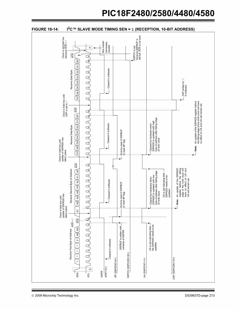
PIC18F2480/2580/4480/4580
FIGURE 18-14: I2C™ SLAVE MODE TIMING SEN = 1 (RECEPTION, 10-BIT ADDRESS)SD
A
SC
L
SSP
IF
BF
(SS
PSTA
T<0>
)
S1
23
45
67
89
12
34
56
78
91
23
45
78
9P
11
11
0A9
A8A7
A6A5
A4A3
A2
A1A0
D7
D6
D5
D4
D3
D1
D0
Rec
eive
Dat
a B
yte
AC
KR
/W =
0
ACK
Rec
eive
Firs
t Byt
e of
Add
ress
Cle
ared
in s
oftw
are
D2 6
(PIR
1<3>
)
Cle
ared
in s
oftw
are
Rec
eive
Sec
ond
Byte
of A
ddre
ss
Cle
ared
by
hard
war
e w
hen
SSPA
DD
is u
pdat
ed w
ith lo
wby
te o
f add
ress
afte
r fal
ling
edge
UA
(SSP
STA
T<1>
)
Clo
ck is
hel
d lo
w u
ntil
upda
te o
f SS
PAD
D h
as
take
n pl
ace
UA
is s
et in
dica
ting
that
the
SSPA
DD
nee
ds to
be
upda
ted
UA
is s
et in
dica
ting
that
SSP
ADD
nee
ds to
be
upda
ted
Cle
ared
by
hard
war
e w
hen
SSPA
DD
is u
pdat
ed w
ith h
igh
byte
of a
ddre
ss a
fter f
allin
g ed
ge
SSP
BUF
is w
ritte
n w
ithco
nten
ts o
f SSP
SR
Dum
my
read
of S
SPB
UF
to c
lear
BF
flag
AC
K
CKP
(SSP
CO
N1<
4>)
12
34
57
89
D7
D6
D5
D4
D3
D1
D0
Rec
eive
Dat
a B
yte
Bus
mas
ter
term
inat
estra
nsfe
r
D2 6
ACK
Cle
ared
in s
oftw
are
Cle
ared
in s
oftw
are
SSPO
V (S
SPC
ON
1<6>
)
CKP
writ
ten
to ‘1
’
Not
e:An
upd
ate
of th
e SS
PAD
D re
gist
er b
efor
eth
e fa
lling
edge
of t
he n
inth
clo
ck w
ill ha
veno
effe
ct o
n U
A a
nd U
A w
ill re
mai
n se
t.
Not
e:An
upd
ate
of t
he S
SPAD
Dre
gist
er
befo
re
the
falli
nged
ge o
f th
e ni
nth
cloc
k w
illha
ve n
o ef
fect
on
UA
and
UA
will
rem
ain
set.
in s
oftw
are
Clo
ck is
hel
d lo
w u
ntil
upda
te o
f SSP
ADD
has
ta
ken
plac
e of n
inth
clo
ckof
nin
th c
lock
SSPO
V is
set
beca
use
SSP
BUF
isst
ill fu
ll. A
CK
is n
ot s
ent.
Dum
my
read
of S
SPB
UF
to c
lear
BF
flag
Clo
ck is
hel
d lo
w u
ntil
CKP
is s
et to
‘1’
Clo
ck is
not
hel
d lo
wbe
caus
e A
CK
= 1
© 2009 Microchip Technology Inc. DS39637D-page 213

PIC18F2480/2580/4480/4580
18.4.5 GENERAL CALL ADDRESSSUPPORTThe addressing procedure for the I2C bus is such thatthe first byte after the Start condition usually deter-mines which device will be the slave addressed by themaster. The exception is the general call address whichcan address all devices. When this address is used, alldevices should, in theory, respond with anAcknowledge.
The general call address is one of eight addressesreserved for specific purposes by the I2C protocol. Itconsists of all ‘0’s with R/W = 0.
The general call address is recognized when theGeneral Call Enable bit (GCEN) is enabled(SSPCON2<7> set). Following a Start bit detect, 8 bitsare shifted into the SSPSR and the address iscompared against the SSPADD. It is also compared tothe general call address and fixed in hardware.
If the general call address matches, the SSPSR istransferred to the SSPBUF, the BF flag bit is set (eighthbit), and on the falling edge of the ninth bit (ACK bit),the SSPIF interrupt flag bit is set.
When the interrupt is serviced, the source for theinterrupt can be checked by reading the contents of theSSPBUF. The value can be used to determine if theaddress was device-specific or a general call address.
In 10-bit mode, the SSPADD is required to be updatedfor the second half of the address to match and the UAbit is set (SSPSTAT<1>). If the general call address issampled when the GCEN bit is set, while the slave isconfigured in 10-Bit Addressing mode, then the secondhalf of the address is not necessary, the UA bit will notbe set and the slave will begin receiving data after theAcknowledge (Figure 18-15).
FIGURE 18-15: SLAVE MODE GENERAL CALL ADDRESS SEQUENCE (7 OR 10-BIT ADDRESSING MODE)
SDA
SCLS
SSPIF
BF (SSPSTAT<0>)
SSPOV (SSPCON1<6>)
Cleared in software
SSPBUF is read
R/W = 0ACKGeneral Call Address
Address is compared to General Call Address
GCEN (SSPCON2<7>)
Receiving Data ACK
1 2 3 4 5 6 7 8 9 1 2 3 4 5 6 7 8 9
D7 D6 D5 D4 D3 D2 D1 D0
after ACK, set interrupt
‘0’
‘1’
DS39637D-page 214 © 2009 Microchip Technology Inc.

PIC18F2480/2580/4480/4580
18.4.6 MASTER MODEMaster mode is enabled by setting and clearing theappropriate SSPM bits in SSPCON1 and by setting theSSPEN bit. In Master mode, the SCL and SDA linesare manipulated by the MSSP hardware.Master mode of operation is supported by interruptgeneration on the detection of the Start and Stopconditions. The Stop (P) and Start (S) bits are clearedfrom a Reset or when the MSSP module is disabled.Control of the I2C bus may be taken when the P bit isset or the bus is Idle, with both the S and P bits clear.
In Firmware Controlled Master mode, user codeconducts all I2C bus operations based on Start andStop bit conditions.
Once Master mode is enabled, the user has sixoptions.
1. Assert a Start condition on SDA and SCL.2. Assert a Repeated Start condition on SDA and
SCL.3. Write to the SSPBUF register initiating
transmission of data/address.4. Configure the I2C port to receive data.5. Generate an Acknowledge condition at the end
of a received byte of data.6. Generate a Stop condition on SDA and SCL.
The following events will cause the MSSP InterruptFlag bit, SSPIF, to be set (MSSP interrupt, if enabled):
• Start condition• Stop condition• Data transfer byte transmitted/received• Acknowledge transmitted• Repeated Start
FIGURE 18-16: MSSP BLOCK DIAGRAM (I2C™ MASTER MODE)
Note: The MSSP module, when configured inI2C Master mode, does not allow queueingof events. For instance, the user is notallowed to initiate a Start condition andimmediately write the SSPBUF register toinitiate transmission before the Startcondition is complete. In this case, theSSPBUF will not be written to and theWCOL bit will be set, indicating that a writeto the SSPBUF did not occur.
Read Write
SSPSR
Start bit, Stop bit,
Start bit Detect
SSPBUF
InternalData Bus
Set/Reset, S, P, WCOL (SSPSTAT);
ShiftClock
MSb LSb
SDA
AcknowledgeGenerate
Stop bit DetectWrite Collision Detect
Clock ArbitrationState Counter forEnd of XMIT/RCV
SCL
SCL In
Bus Collision
SDA In
Rec
eive
Ena
ble
Clo
ck C
ntl
Clo
ck A
rbitr
ate/
WC
OL
Det
ect
(hol
d of
f clo
ck s
ourc
e)
SSPADD<6:0>
Baud
Set SSPIF, BCLIF;Reset ACKSTAT, PEN (SSPCON2)
RateGenerator
SSPM<3:0>
© 2009 Microchip Technology Inc. DS39637D-page 215
PIC18F2480/2580/4480/4580
18.4.6.1 I2C Master Mode OperationThe master device generates all of the serial clockpulses and the Start and Stop conditions. A transfer isended with a Stop condition or with a Repeated Startcondition. Since the Repeated Start condition is alsothe beginning of the next serial transfer, the I2C bus willnot be released.In Master Transmitter mode, serial data is outputthrough SDA while SCL outputs the serial clock. Thefirst byte transmitted contains the slave address of thereceiving device (7 bits) and the Read/Write (R/W) bit.In this case, the R/W bit will be logic ‘0’. Serial data istransmitted 8 bits at a time. After each byte is transmit-ted, an Acknowledge bit is received. Start and Stopconditions are output to indicate the beginning and theend of a serial transfer.
In Master Receive mode, the first byte transmitted con-tains the slave address of the transmitting device(7 bits) and the R/W bit. In this case, the R/W bit will belogic ‘1’ Thus, the first byte transmitted is a 7-bit slaveaddress followed by a ‘1’ to indicate the receive bit.Serial data is received via SDA, while SCL outputs theserial clock. Serial data is received 8 bits at a time. Aftereach byte is received, an Acknowledge bit is transmit-ted. Start and Stop conditions indicate the beginningand end of transmission.
The Baud Rate Generator used for the SPI mode oper-ation is used to set the SCL clock frequency for either100 kHz, 400 kHz or 1 MHz I2C operation. SeeSection 18.4.7 “Baud Rate” for more details.
A typical transmit sequence would go as follows:
1. The user generates a Start condition by settingthe Start Enable bit, SEN (SSPCON2<0>).
2. SSPIF is set. The MSSP module will wait therequired start time before any other operationtakes place.
3. The user loads the SSPBUF with the slaveaddress to transmit.
4. Address is shifted out the SDA pin until all 8 bitsare transmitted.
5. The MSSP module shifts in the ACK bit from theslave device and writes its value into theSSPCON2 register (SSPCON2<6>).
6. The MSSP module generates an interrupt at theend of the ninth clock cycle by setting the SSPIFbit.
7. The user loads the SSPBUF with eight bits ofdata.
8. Data is shifted out the SDA pin until all 8 bits aretransmitted.
9. The MSSP module shifts in the ACK bit from theslave device and writes its value into theSSPCON2 register (SSPCON2<6>).
10. The MSSP module generates an interrupt at theend of the ninth clock cycle by setting the SSPIFbit.
11. The user generates a Stop condition by settingthe Stop Enable bit, PEN (SSPCON2<2>).
12. Interrupt is generated once the Stop condition iscomplete.
DS39637D-page 216 © 2009 Microchip Technology Inc.

PIC18F2480/2580/4480/4580
18.4.7 BAUD RATE In I2C Master mode, the Baud Rate Generator (BRG)reload value is placed in the lower 7 bits of theSSPADD register (Figure 18-17). When a write occursto SSPBUF, the Baud Rate Generator will automaticallybegin counting. The BRG counts down and stops untilanother reload has taken place. The BRG count isdecremented twice per instruction cycle (TCY) on theQ2 and Q4 clocks. In I2C Master mode, the BRG isreloaded automatically.Once the given operation is complete (i.e., transmis-sion of the last data bit is followed by ACK), the internalclock will automatically stop counting and the SCL pinwill remain in its last state.
Table 18-3 demonstrates clock rates based oninstruction cycles and the BRG value loaded intoSSPADD.
FIGURE 18-17: BAUD RATE GENERATOR BLOCK DIAGRAM
TABLE 18-3: I2C™ CLOCK RATE W/BRG
FCY FCY*2 BRG Value FSCL (2 Rollovers of BRG)
10 MHz 20 MHz 19h 400 kHz10 MHz 20 MHz 20h 312.5 kHz10 MHz 20 MHz 64h 100 kHz4 MHz 8 MHz 0Ah 400 kHz4 MHz 8 MHz 0Dh 308 kHz4 MHz 8 MHz 28h 100 kHz1 MHz 2 MHz 03h 333 kHz1 MHz 2 MHz 0Ah 100 kHz
SSPM<3:0>
BRG Down CounterCLKO FOSC/4
SSPADD<6:0>
SSPM<3:0>
SCL
ReloadControl
Reload
© 2009 Microchip Technology Inc. DS39637D-page 217

PIC18F2480/2580/4480/4580
18.4.7.1 Clock ArbitrationClock arbitration occurs when the master, during anyreceive, transmit or Repeated Start/Stop condition,deasserts the SCL pin (SCL allowed to float high).When the SCL pin is allowed to float high, the BaudRate Generator (BRG) is suspended from countinguntil the SCL pin is actually sampled high. When theSCL pin is sampled high, the Baud Rate Generator isreloaded with the contents of SSPADD<6:0> andbegins counting. This ensures that the SCL high timewill always be at least one BRG rollover count in theevent that the clock is held low by an external device(Figure 18-18).
FIGURE 18-18: BAUD RATE GENERATOR TIMING WITH CLOCK ARBITRATION
SDA
SCL
SCL deasserted but slave holds
DX – 1DX
BRG
SCL is sampled high, reload takesplace and BRG starts its count
03h 02h 01h 00h (hold off) 03h 02h
Reload
BRGValue
SCL low (clock arbitration)SCL allowed to transition high
BRG decrements onQ2 and Q4 cycles
DS39637D-page 218 © 2009 Microchip Technology Inc.
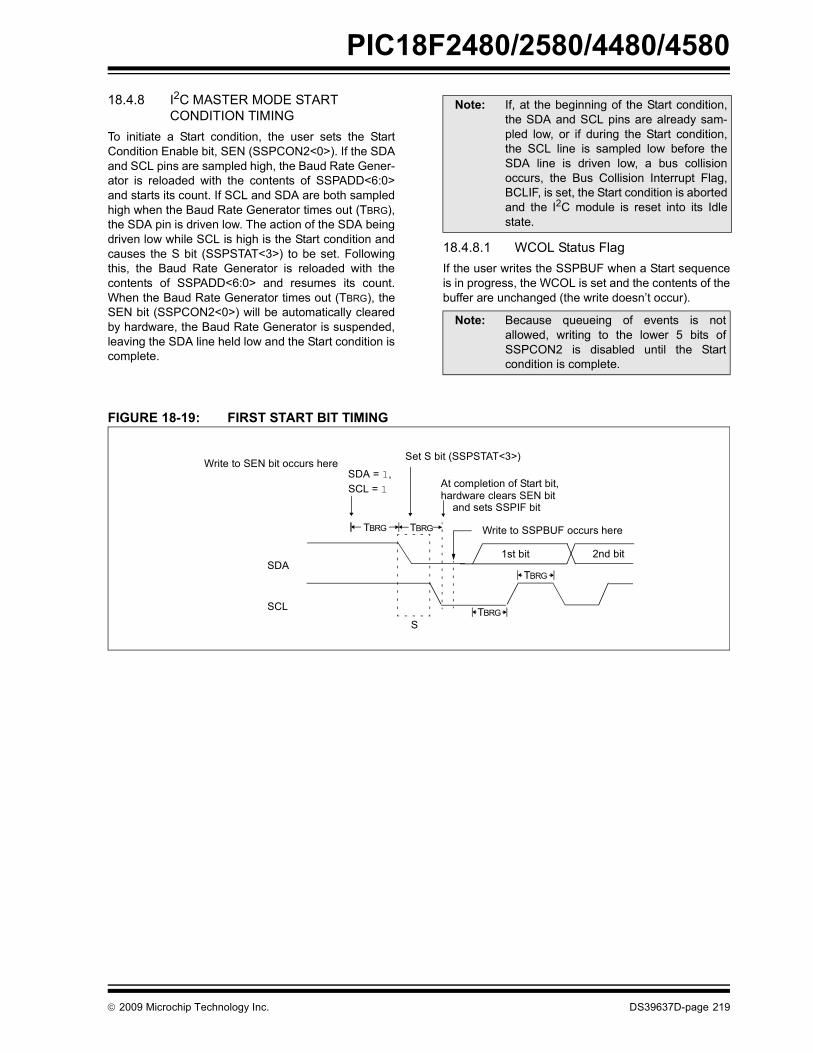
PIC18F2480/2580/4480/4580
18.4.8 I2C MASTER MODE STARTCONDITION TIMINGTo initiate a Start condition, the user sets the StartCondition Enable bit, SEN (SSPCON2<0>). If the SDAand SCL pins are sampled high, the Baud Rate Gener-ator is reloaded with the contents of SSPADD<6:0>and starts its count. If SCL and SDA are both sampledhigh when the Baud Rate Generator times out (TBRG),the SDA pin is driven low. The action of the SDA beingdriven low while SCL is high is the Start condition andcauses the S bit (SSPSTAT<3>) to be set. Followingthis, the Baud Rate Generator is reloaded with thecontents of SSPADD<6:0> and resumes its count.When the Baud Rate Generator times out (TBRG), theSEN bit (SSPCON2<0>) will be automatically clearedby hardware, the Baud Rate Generator is suspended,leaving the SDA line held low and the Start condition iscomplete.
18.4.8.1 WCOL Status FlagIf the user writes the SSPBUF when a Start sequenceis in progress, the WCOL is set and the contents of thebuffer are unchanged (the write doesn’t occur).
FIGURE 18-19: FIRST START BIT TIMING
Note: If, at the beginning of the Start condition,the SDA and SCL pins are already sam-pled low, or if during the Start condition,the SCL line is sampled low before theSDA line is driven low, a bus collisionoccurs, the Bus Collision Interrupt Flag,BCLIF, is set, the Start condition is abortedand the I2C module is reset into its Idlestate.
Note: Because queueing of events is notallowed, writing to the lower 5 bits ofSSPCON2 is disabled until the Startcondition is complete.
SDA
SCL
S
TBRG
1st bit 2nd bit
TBRG
SDA = 1, At completion of Start bit,SCL = 1
Write to SSPBUF occurs hereTBRG
hardware clears SEN bit
TBRG
Write to SEN bit occurs hereSet S bit (SSPSTAT<3>)
and sets SSPIF bit
© 2009 Microchip Technology Inc. DS39637D-page 219

PIC18F2480/2580/4480/4580
18.4.9 I2C MASTER MODE REPEATEDSTART CONDITION TIMINGA Repeated Start condition occurs when the RSEN bit(SSPCON2<1>) is programmed high and the I2C logicmodule is in the Idle state. When the RSEN bit is set,the SCL pin is asserted low. When the SCL pin is sam-pled low, the Baud Rate Generator is loaded with thecontents of SSPADD<5:0> and begins counting. TheSDA pin is released (brought high) for one Baud RateGenerator count (TBRG). When the Baud Rate Genera-tor times out, and if SDA is sampled high, the SCL pinwill be deasserted (brought high). When SCL is sam-pled high, the Baud Rate Generator is reloaded withthe contents of SSPADD<6:0> and begins counting.SDA and SCL must be sampled high for one TBRG.This action is then followed by assertion of the SDA pin(SDA = 0) for one TBRG while SCL is high. Followingthis, the RSEN bit (SSPCON2<1>) will be automaticallycleared and the Baud Rate Generator will not bereloaded, leaving the SDA pin held low. As soon as aStart condition is detected on the SDA and SCL pins,the S bit (SSPSTAT<3>) will be set. The SSPIF bit willnot be set until the Baud Rate Generator has timed out.
Immediately following the SSPIF bit getting set, the usermay write the SSPBUF with the 7-bit address in 7-bitmode, or the default first address in 10-bit mode. Afterthe first eight bits are transmitted and an ACK isreceived, the user may then transmit an additional eightbits of address (10-bit mode) or eight bits of data (7-bitmode).
18.4.9.1 WCOL Status FlagIf the user writes the SSPBUF when a Repeated Startsequence is in progress, the WCOL is set and thecontents of the buffer are unchanged (the write doesn’toccur).
FIGURE 18-20: REPEAT START CONDITION WAVEFORM
Note 1: If RSEN is programmed while any otherevent is in progress, it will not take effect.
2: A bus collision during the Repeated Startcondition occurs if:
• SDA is sampled low when SCL goes from low-to-high.
• SCL goes low before SDA is asserted low. This may indicate that another master is attempting to transmit a data ‘1’.
Note: Because queueing of events is notallowed, writing of the lower 5 bits ofSSPCON2 is disabled until the RepeatedStart condition is complete.
SDA
SCL
Sr = Repeated Start
Write to SSPCON2
Write to SSPBUF occurs hereFalling edge of ninth clock,end of XMIT
At completion of Start bit, hardware clears RSEN bit
1st bit
Set S (SSPSTAT<3>)
TBRG
TBRG
SDA = 1,
SDA = 1,
SCL (no change).SCL = 1
occurs here.
TBRG TBRG TBRG
and sets SSPIF
DS39637D-page 220 © 2009 Microchip Technology Inc.

PIC18F2480/2580/4480/4580
18.4.10 I2C MASTER MODETRANSMISSIONTransmission of a data byte, a 7-bit address or theother half of a 10-bit address is accomplished by simplywriting a value to the SSPBUF register. This action willset the Buffer Full flag bit, BF, and allow the Baud RateGenerator to begin counting and start the next trans-mission. Each bit of address/data will be shifted outonto the SDA pin after the falling edge of SCL isasserted (see data hold time specification parameter106). SCL is held low for one Baud Rate Generator roll-over count (TBRG). Data should be valid before SCL isreleased high (see data setup time specificationparameter 107). When the SCL pin is released high, itis held that way for TBRG. The data on the SDA pinmust remain stable for that duration and some holdtime after the next falling edge of SCL. After the eighthbit is shifted out (the falling edge of the eighth clock),the BF flag is cleared and the master releases SDA.This allows the slave device being addressed torespond with an ACK bit during the ninth bit time if anaddress match occurred, or if data was receivedproperly. The status of ACK is written into the ACKDTbit on the falling edge of the ninth clock. If the masterreceives an Acknowledge, the Acknowledge status bit,ACKSTAT, is cleared. If not, the bit is set. After the ninthclock, the SSPIF bit is set and the master clock (BaudRate Generator) is suspended until the next data byteis loaded into the SSPBUF, leaving SCL low and SDAunchanged (Figure 18-21).
After the write to the SSPBUF, each bit of address willbe shifted out on the falling edge of SCL until all sevenaddress bits and the R/W bit are completed. On the fall-ing edge of the eighth clock, the master will deassertthe SDA pin, allowing the slave to respond with anAcknowledge. On the falling edge of the ninth clock, themaster will sample the SDA pin to see if the addresswas recognized by a slave. The status of the ACK bit isloaded into the ACKSTAT status bit (SSPCON2<6>).Following the falling edge of the ninth clock transmis-sion of the address, the SSPIF flag is set, the BF flag iscleared and the Baud Rate Generator is turned off untilanother write to the SSPBUF takes place, holding SCLlow and allowing SDA to float.
18.4.10.1 BF Status FlagIn Transmit mode, the BF bit (SSPSTAT<0>) is setwhen the CPU writes to SSPBUF and is cleared whenall 8 bits are shifted out.
18.4.10.2 WCOL Status FlagIf the user writes the SSPBUF when a transmit isalready in progress (i.e., SSPSR is still shifting out adata byte), the WCOL is set and the contents of the buf-fer are unchanged (the write doesn’t occur).
WCOL must be cleared in software.
18.4.10.3 ACKSTAT Status FlagIn Transmit mode, the ACKSTAT bit (SSPCON2<6>) iscleared when the slave has sent an Acknowledge(ACK = 0) and is set when the slave does not Acknowl-edge (ACK = 1). A slave sends an Acknowledge whenit has recognized its address (including a general call),or when the slave has properly received its data.
18.4.11 I2C MASTER MODE RECEPTIONMaster mode reception is enabled by programming theReceive Enable bit, RCEN (SSPCON2<3>).
The Baud Rate Generator begins counting and on eachrollover, the state of the SCL pin changes (high-to-low/low-to-high) and data is shifted into the SSPSR. Afterthe falling edge of the eighth clock, the receive enableflag is automatically cleared, the contents of theSSPSR are loaded into the SSPBUF, the BF flag bit isset, the SSPIF flag bit is set and the Baud RateGenerator is suspended from counting, holding SCLlow. The MSSP is now in Idle state awaiting the nextcommand. When the buffer is read by the CPU, the BFflag bit is automatically cleared. The user can thensend an Acknowledge bit at the end of reception bysetting the Acknowledge sequence enable bit, ACKEN(SSPCON2<4>).
18.4.11.1 BF Status FlagIn receive operation, the BF bit is set when an addressor data byte is loaded into SSPBUF from SSPSR. It iscleared when the SSPBUF register is read.
18.4.11.2 SSPOV Status FlagIn receive operation, the SSPOV bit is set when 8 bitsare received into the SSPSR and the BF flag bit isalready set from a previous reception.
18.4.11.3 WCOL Status FlagIf the user writes the SSPBUF when a receive isalready in progress (i.e., SSPSR is still shifting in a databyte), the WCOL bit is set and the contents of the bufferare unchanged (the write doesn’t occur).
Note: The MSSP module must be in an Idle statebefore the RCEN bit is set or the RCEN bitwill be disregarded.
© 2009 Microchip Technology Inc. DS39637D-page 221

PIC18F2480/2580/4480/4580
FIGURE 18-21: I2C™ MASTER MODE WAVEFORM (TRANSMISSION, 7 OR 10-BIT ADDRESS)SD
A
SC
L
SS
PIF
BF
(SS
PS
TAT<
0>)
SE
N
A7A
6A5
A4A
3A
2A1
AC
K =
0D
7D
6D
5D
4D
3D
2D
1D
0
AC
KTr
ansm
ittin
g D
ata
or S
econ
d H
alf
R/W
= 0
Tran
smit
Addr
ess
to S
lave
12
34
56
78
91
23
45
67
89
P
Cle
ared
in s
oftw
are
serv
ice
rout
ine
SS
PB
UF
is w
ritte
n in
sof
twar
e
from
MS
SP
inte
rrup
t
Afte
r Sta
rt co
nditi
on, S
EN c
lear
ed b
y ha
rdw
are
S
SS
PB
UF
writ
ten
with
7-b
it ad
dres
s an
d R
/W,
star
t tra
nsm
it
SC
L he
ld lo
ww
hile
CP
Ure
spon
ds to
SS
PIF
SE
N =
0
of 1
0-bi
t Add
ress
Writ
e S
SP
CO
N2<
0> S
EN
= 1
Star
t con
ditio
n be
gins
From
sla
ve, c
lear
AC
KS
TAT
bit S
SPC
ON
2<6>
AC
KS
TAT
in
SS
PC
ON
2 = 1
Cle
ared
in s
oftw
are
SSP
BU
F w
ritte
n
PE
N
R/W
Cle
ared
in s
oftw
are
DS39637D-page 222 © 2009 Microchip Technology Inc.

PIC18F2480/2580/4480/4580
FIGURE 18-22: I2C™ MASTER MODE WAVEFORM (RECEPTION, 7-BIT ADDRESS)P9
87
65
D0
D1
D2
D3
D4
D5
D6
D7
S
A7
A6
A5
A4
A3
A2
A1
SD
A
SC
L1
23
45
67
89
12
34
56
78
91
23
4
Bus
mas
ter
term
inat
estra
nsfe
r
ACK
Rec
eivi
ng D
ata
from
Sla
veR
ecei
ving
Dat
a fro
m S
lave
D0
D1
D2
D3
D4
D5
D6
D7
ACK
R/W
= 1
Tran
smit
Addr
ess
to S
lave
SS
PIF
BF
AC
K is
not
sen
t
Writ
e to
SS
PCO
N2<
0>(S
EN =
1),
Writ
e to
SS
PBU
F oc
curs
her
e,AC
K fr
om S
laveM
aste
r con
figur
ed a
s a
rece
iver
by p
rogr
amm
ing
SSP
CO
N2<
3> (R
CEN
= 1
)PE
N b
it = 1
writ
ten
here
Dat
a sh
ifted
in o
n fa
lling
edge
of C
LK
Cle
ared
in s
oftw
are
star
t XM
IT
SEN
= 0
SS
PO
V
SDA
= 0
, SC
L = 1
whi
le C
PU
(SSP
STA
T<0>
)
AC
K
Cle
ared
in s
oftw
are
Cle
ared
in s
oftw
are
Set
SSP
IF in
terru
ptat
end
of r
ecei
ve
Set P
bit
(SSP
STAT
<4>)
and
SSPI
FC
lear
ed in
softw
are
AC
K fro
m M
aste
r
Set S
SPI
F at
end
Set S
SPIF
inte
rrupt
at e
nd o
f Ack
now
ledg
ese
quen
ce
Set
SSP
IF in
terru
ptat
end
of A
ckno
wle
dge
sequ
ence
of re
ceiv
e
Set A
CKE
N, s
tart
Ackn
owle
dge
sequ
ence
SSP
OV
is s
et b
ecau
seS
SPB
UF
is s
till f
ull
SD
A =
ACK
DT
= 1
RC
EN c
lear
edau
tom
atic
ally
RC
EN =
1, s
tart
next
rece
ive
Writ
e to
SSP
CO
N2<
4>to
sta
rt Ac
know
ledg
e se
quen
ceSD
A =
ACK
DT
(SSP
CO
N2<
5>) =
0
RC
EN c
lear
edau
tom
atic
ally
resp
onds
to S
SPIF
AC
KE
Nbegi
n St
art C
ondi
tion
Cle
ared
in s
oftw
are
SDA
= A
CKD
T = 0
Last
bit
is s
hifte
d in
to S
SPSR
and
cont
ents
are
unl
oade
d in
to S
SPB
UF
© 2009 Microchip Technology Inc. DS39637D-page 223

PIC18F2480/2580/4480/4580
18.4.12 ACKNOWLEDGE SEQUENCETIMINGAn Acknowledge sequence is enabled by setting theAcknowledge sequence enable bit, ACKEN(SSPCON2<4>). When this bit is set, the SCL pin ispulled low and the contents of the Acknowledge data bitare presented on the SDA pin. If the user wishes to gen-erate an Acknowledge, then the ACKDT bit should becleared. If not, the user should set the ACKDT bit beforestarting an Acknowledge sequence. The Baud RateGenerator then counts for one rollover period (TBRG)and the SCL pin is deasserted (pulled high). When theSCL pin is sampled high (clock arbitration), the BaudRate Generator counts for TBRG; the SCL pin is thenpulled low. Following this, the ACKEN bit is automaticallycleared, the Baud Rate Generator is turned off and theMSSP module then goes into Idle mode (Figure 18-23).
18.4.12.1 WCOL Status FlagIf the user writes the SSPBUF when an Acknowledgesequence is in progress, then WCOL is set and thecontents of the buffer are unchanged (the write doesn’toccur).
18.4.13 STOP CONDITION TIMINGA Stop bit is asserted on the SDA pin at the end of areceive/transmit by setting the Stop Sequence Enablebit, PEN (SSPCON2<2>). At the end of a receive/transmit, the SCL line is held low after the falling edgeof the ninth clock. When the PEN bit is set, the masterwill assert the SDA line low. When the SDA line is sam-pled low, the Baud Rate Generator is reloaded andcounts down to 0. When the Baud Rate Generatortimes out, the SCL pin will be brought high and oneTBRG (Baud Rate Generator rollover count) later, theSDA pin will be deasserted. When the SDA pin issampled high while SCL is high, the P bit(SSPSTAT<4>) is set. A TBRG later, the PEN bit iscleared and the SSPIF bit is set (Figure 18-24).
18.4.13.1 WCOL Status FlagIf the user writes the SSPBUF when a Stop sequenceis in progress, then the WCOL bit is set and thecontents of the buffer are unchanged (the write doesn’toccur).
FIGURE 18-23: ACKNOWLEDGE SEQUENCE WAVEFORM
FIGURE 18-24: STOP CONDITION RECEIVE OR TRANSMIT MODE
Note: TBRG = one Baud Rate Generator period.
SDA
SCL
Set SSPIF at the
Acknowledge sequence starts here,write to SSPCON2 ACKEN automatically cleared
Cleared in
TBRG TBRG
end of receive
8
ACKEN = 1, ACKDT = 0
D0
9
SSPIF
software Set SSPIF at the endof Acknowledge sequence
Cleared insoftware
ACK
SCL
SDA
SDA asserted low before rising edge of clock
Write to SSPCON2,set PEN
Falling edge of
SCL = 1 for TBRG, followed by SDA = 1 for TBRG
9th clock
SCL brought high after TBRG
Note: TBRG = one Baud Rate Generator period.
TBRG TBRG
after SDA sampled high, P bit (SSPSTAT<4>) is set
TBRG
to set up Stop condition
ACK
PTBRG
PEN bit (SSPCON2<2>) is cleared byhardware and the SSPIF bit is set
DS39637D-page 224 © 2009 Microchip Technology Inc.

PIC18F2480/2580/4480/4580
18.4.14 SLEEP OPERATIONWhile in Sleep mode, the I2C module can receiveaddresses or data and when an address match orcomplete byte transfer occurs, wake the processorfrom Sleep (if the MSSP interrupt is enabled).18.4.15 EFFECT OF A RESETA Reset disables the MSSP module and terminates thecurrent transfer.
18.4.16 MULTI-MASTER MODEIn Multi-Master mode, the interrupt generation on thedetection of the Start and Stop conditions allows thedetermination of when the bus is free. The Stop (P) andStart (S) bits are cleared from a Reset or when theMSSP module is disabled. Control of the I2C bus maybe taken when the P bit (SSPSTAT<4>) is set, or thebus is Idle, with both the S and P bits clear. When thebus is busy, enabling the MSSP interrupt will generatethe interrupt when the Stop condition occurs.
In multi-master operation, the SDA line must bemonitored for arbitration to see if the signal level is theexpected output level. This check is performed inhardware with the result placed in the BCLIF bit.
The states where arbitration can be lost are:
• Address Transfer • Data Transfer• A Start Condition • A Repeated Start Condition• An Acknowledge Condition
18.4.17 MULTI-MASTER COMMUNICATION, BUS COLLISION AND BUS ARBITRATION
Multi-Master mode support is achieved by bus arbitra-tion. When the master outputs address/data bits ontothe SDA pin, arbitration takes place when the masteroutputs a ‘1’ on SDA, by letting SDA float high, andanother master asserts a ‘0’. When the SCL pin floatshigh, data should be stable. If the expected data onSDA is a ‘1’ and the data sampled on the SDA pin = 0,then a bus collision has taken place. The master will setthe Bus Collision Interrupt Flag, BCLIF, and reset theI2C port to its Idle state (Figure 18-25).
If a transmit was in progress when the bus collisionoccurred, the transmission is halted, the BF flag iscleared, the SDA and SCL lines are deasserted and theSSPBUF can be written to. When the user services thebus collision Interrupt Service Routine and if the I2Cbus is free, the user can resume communication byasserting a Start condition.
If a Start, Repeated Start, Stop or Acknowledgecondition was in progress when the bus collisionoccurred, the condition is aborted, the SDA and SCLlines are deasserted and the respective control bits inthe SSPCON2 register are cleared. When the user ser-vices the bus collision Interrupt Service Routine, and ifthe I2C bus is free, the user can resume communicationby asserting a Start condition.
The master will continue to monitor the SDA and SCLpins. If a Stop condition occurs, the SSPIF bit will be set.
A write to the SSPBUF will start the transmission ofdata at the first data bit, regardless of where thetransmitter left off when the bus collision occurred.
In Multi-Master mode, the interrupt generation on thedetection of Start and Stop conditions allows the determi-nation of when the bus is free. Control of the I2C bus canbe taken when the P bit is set in the SSPSTAT register,or the bus is Idle and the S and P bits are cleared.
FIGURE 18-25: BUS COLLISION TIMING FOR TRANSMIT AND ACKNOWLEDGE
SDA
SCL
BCLIF
SDA released
SDA line pulled lowby another source
Sample SDA. While SCL is high,data doesn’t match what is driven
bus collision has occurred.
Set bus collisioninterrupt (BCLIF)
by the master;
by master
Data changeswhile SCL = 0
© 2009 Microchip Technology Inc. DS39637D-page 225

PIC18F2480/2580/4480/4580
18.4.17.1 Bus Collision During a StartConditionDuring a Start condition, a bus collision occurs if:
a) SDA or SCL is sampled low at the beginning ofthe Start condition (Figure 18-26).
b) SCL is sampled low before SDA is asserted low(Figure 18-27).
During a Start condition, both the SDA and the SCLpins are monitored.
If the SDA pin is already low, or the SCL pin is alreadylow, then all of the following occur:• the Start condition is aborted, • the BCLIF flag is set; and• the MSSP module is reset to its Idle state
(Figure 18-26)
The Start condition begins with the SDA and SCL pinsdeasserted. When the SDA pin is sampled high, theBaud Rate Generator is loaded from SSPADD<6:0>and counts down to 0. If the SCL pin is sampled lowwhile SDA is high, a bus collision occurs because it isassumed that another master is attempting to drive adata ‘1’ during the Start condition.
If the SDA pin is sampled low during this count, theBRG is reset and the SDA line is asserted early(Figure 18-28). If, however, a ‘1’ is sampled on the SDApin, the SDA pin is asserted low at the end of the BRGcount. The Baud Rate Generator is then reloaded andcounts down to 0 and during this time, if the SCL pinsare sampled as ‘0’, a bus collision does not occur. Atthe end of the BRG count, the SCL pin is asserted low.
FIGURE 18-26: BUS COLLISION DURING START CONDITION (SDA ONLY)
Note: The reason that bus collision is not a factorduring a Start condition is that no two busmasters can assert a Start condition at theexact same time. Therefore, one masterwill always assert SDA before the other.This condition does not cause a buscollision because the two masters must beallowed to arbitrate the first addressfollowing the Start condition. If the addressis the same, arbitration must be allowed tocontinue into the data portion, RepeatedStart or Stop conditions.
SDA
SCL
SEN
SDA sampled low before
SDA goes low before the SEN bit is set.
S bit and SSPIF set because
MSSP module reset into Idle state.SEN cleared automatically because of bus collision.
S bit and SSPIF set because
Set SEN, enable Startcondition if SDA = 1, SCL = 1
SDA = 0, SCL = 1.
BCLIF
S
SSPIF
SDA = 0, SCL = 1.
SSPIF and BCLIF arecleared in software
SSPIF and BCLIF arecleared in software
Set BCLIF,
Start condition. Set BCLIF.
DS39637D-page 226 © 2009 Microchip Technology Inc.

PIC18F2480/2580/4480/4580
FIGURE 18-27: BUS COLLISION DURING START CONDITION (SCL = 0)FIGURE 18-28: BRG RESET DUE TO SDA ARBITRATION DURING START CONDITION
SDA
SCL
SENbus collision occurs. Set BCLIF.SCL = 0 before SDA = 0,
Set SEN, enable Startsequence if SDA = 1, SCL = 1
TBRG TBRG
SDA = 0, SCL = 1
BCLIF
S
SSPIF
Interrupt clearedin software
bus collision occurs. Set BCLIF.SCL = 0 before BRG time-out,
‘0’ ‘0’
‘0’‘0’
SDA
SCL
SEN
Set S
Set SEN, enable STARTsequence if SDA = 1, SCL = 1
Less than TBRG TBRG
SDA = 0, SCL = 1
BCLIF
S
SSPIF
S
Interrupts clearedin softwareset SSPIF
SDA = 0, SCL = 1,
SDA pulled low by other master.Reset BRG and assert SDA.
SCL pulled low after BRGtime-out
Set SSPIF
‘0’
© 2009 Microchip Technology Inc. DS39637D-page 227

PIC18F2480/2580/4480/4580
18.4.17.2 Bus Collision During a RepeatedStart ConditionDuring a Repeated Start condition, a bus collisionoccurs if:
a) A low level is sampled on SDA when SCL goesfrom a low level to a high level.
b) SCL goes low before SDA is asserted low, indi-cating that another master is attempting totransmit a data ‘1’.
When the user deasserts SDA and the pin is allowed tofloat high, the BRG is loaded with SSPADD<6:0> andcounts down to 0. The SCL pin is then deasserted andwhen sampled high, the SDA pin is sampled.
If SDA is low, a bus collision has occurred (i.e., anothermaster is attempting to transmit a data ‘0’, seeFigure 18-29). If SDA is sampled high, the BRG isreloaded and begins counting. If SDA goes from high-to-low before the BRG times out, no bus collision occursbecause no two masters can assert SDA at exactly thesame time.
If SCL goes from high-to-low before the BRG times out,and SDA has not already been asserted, a bus collisionoccurs. In this case, another master is attempting totransmit a data ‘1’ during the Repeated Start condition,see Figure 18-30.
If, at the end of the BRG time-out, both SCL and SDAare still high, the SDA pin is driven low and the BRG isreloaded and begins counting. At the end of the countregardless of the status of the SCL pin, the SCL pin isdriven low and the Repeated Start condition iscomplete.
FIGURE 18-29: BUS COLLISION DURING A REPEATED START CONDITION (CASE 1)
FIGURE 18-30: BUS COLLISION DURING REPEATED START CONDITION (CASE 2)
SDA
SCL
RSEN
BCLIF
S
SSPIF
Sample SDA when SCL goes high.If SDA = 0, set BCLIF and release SDA and SCL.
Cleared in software
‘0’
‘0’
SDA
SCL
BCLIF
RSEN
S
SSPIF
Interrupt clearedin software
SCL goes low before SDA,set BCLIF. Release SDA and SCL.
TBRG TBRG
‘0’
DS39637D-page 228 © 2009 Microchip Technology Inc.

PIC18F2480/2580/4480/4580
18.4.17.3 Bus Collision During a StopConditionBus collision occurs during a Stop condition if:
a) After the SDA pin has been deasserted andallowed to float high, SDA is sampled low afterthe BRG has timed out.
b) After the SCL pin is deasserted, SCL is sampledlow before SDA goes high.
The Stop condition begins with SDA asserted low.When SDA is sampled low, the SCL pin is allowed tofloat. When the pin is sampled high (clock arbitration),the Baud Rate Generator is loaded with SSPADD<6:0>and counts down to 0. After the BRG times out, SDA issampled. If SDA is sampled low, a bus collision hasoccurred. This is due to another master attempting todrive a data ‘0’ (Figure 18-31). If the SCL pin issampled low before SDA is allowed to float high, a buscollision occurs. This is another case of another masterattempting to drive a data ‘0’ (Figure 18-32).
FIGURE 18-31: BUS COLLISION DURING A STOP CONDITION (CASE 1)
FIGURE 18-32: BUS COLLISION DURING A STOP CONDITION (CASE 2)
SDA
SCL
BCLIF
PEN
P
SSPIF
TBRG TBRG TBRG
SDA asserted low
SDA sampledlow after TBRG,set BCLIF
‘0’
‘0’
SDA
SCL
BCLIF
PEN
P
SSPIF
TBRG TBRG TBRG
Assert SDA SCL goes low before SDA goes high,set BCLIF
‘0’
‘0’
© 2009 Microchip Technology Inc. DS39637D-page 229

PIC18F2480/2580/4480/4580
NOTES:DS39637D-page 230 © 2009 Microchip Technology Inc.

PIC18F2480/2580/4480/4580
19.0 ENHANCED UNIVERSAL SYNCHRONOUS RECEIVER TRANSMITTER (EUSART)
The Universal Synchronous Asynchronous ReceiverTransmitter (USART) module is one of the two serialI/O modules. (USART is also known as a SerialCommunications Interface or SCI.) The USART can beconfigured as a full-duplex asynchronous system thatcan communicate with peripheral devices, such asCRT terminals and personal computers. It can also beconfigured as a half-duplex synchronous system thatcan communicate with peripheral devices, such as A/Dor D/A integrated circuits, serial EEPROMs and so on.
The EUSART module implements additional features,including automatic baud rate detection and calibra-tion, automatic wake-up on Sync Break reception and12-bit Break character transmit. These make it ideallysuited for use in Local Interconnect Network bus(LIN/J2602 bus) systems.
The EUSART can be configured in the followingmodes:
• Asynchronous (full-duplex) with:- Auto-wake-up on character reception- Auto-baud calibration- 12-bit Break character transmission
• Synchronous – Master (half-duplex) with selectable clock polarity
• Synchronous – Slave (half-duplex) with selectable clock polarity
The pins of the Enhanced USART are multiplexed withPORTC. In order to configure RC6/TX/CK andRC7/RX/DT as a USART:
• bit, SPEN (RCSTA<7>), must be set (= 1)• bit, TRISC<7>, must be set (= 1)• bit, TRISC<6>, must be cleared (= 0) for
Asynchronous and Synchronous Master modes, or set (= 1) for Synchronous Slave mode
The operation of the Enhanced USART module iscontrolled through three registers:
• Transmit Status and Control (TXSTA)• Receive Status and Control (RCSTA)• Baud Rate Control (BAUDCON)
These are detailed on the following pages inRegister 19-1, Register 19-2 and Register 19-3,respectively.
Note: The EUSART control will automaticallyreconfigure the pin from input to output asneeded.
© 2009 Microchip Technology Inc. DS39637D-page 231

PIC18F2480/2580/4480/4580
REGISTER 19-1: TXSTA: TRANSMIT STATUS AND CONTROL REGISTERR/W-0 R/W-0 R/W-0 R/W-0 R/W-0 R/W-0 R-1 R/W-0CSRC TX9 TXEN(1) SYNC SENDB BRGH TRMT TX9D
bit 7 bit 0
Legend:R = Readable bit W = Writable bit U = Unimplemented bit, read as ‘0’-n = Value at POR ‘1’ = Bit is set ‘0’ = Bit is cleared x = Bit is unknown
bit 7 CSRC: Clock Source Select bitAsynchronous mode: Don’t care.Synchronous mode: 1 = Master mode (clock generated internally from BRG)0 = Slave mode (clock from external source)
bit 6 TX9: 9-Bit Transmit Enable bit 1 = Selects 9-bit transmission 0 = Selects 8-bit transmission
bit 5 TXEN: Transmit Enable bit(1)
1 = Transmit enabled0 = Transmit disabled
bit 4 SYNC: EUSART Mode Select bit 1 = Synchronous mode 0 = Asynchronous mode
bit 3 SENDB: Send Break Character bitAsynchronous mode:1 = Send Sync Break on next transmission (cleared by hardware upon completion)0 = Sync Break transmission completedSynchronous mode:Don’t care.
bit 2 BRGH: High Baud Rate Select bit Asynchronous mode: 1 = High speed 0 = Low speedSynchronous mode: Unused in this mode.
bit 1 TRMT: Transmit Shift Register Status bit1 = TSR empty 0 = TSR full
bit 0 TX9D: 9th bit of Transmit DataCan be address/data bit or a parity bit.
Note 1: SREN/CREN overrides TXEN in Sync mode.
DS39637D-page 232 © 2009 Microchip Technology Inc.

PIC18F2480/2580/4480/4580
REGISTER 19-2: RCSTA: RECEIVE STATUS AND CONTROL REGISTERR/W-0 R/W-0 R/W-0 R/W-0 R/W-0 R-0 R-0 R-xSPEN RX9 SREN CREN ADDEN FERR OERR RX9D
bit 7 bit 0
Legend:R = Readable bit W = Writable bit U = Unimplemented bit, read as ‘0’-n = Value at POR ‘1’ = Bit is set ‘0’ = Bit is cleared x = Bit is unknown
bit 7 SPEN: Serial Port Enable bit1 = Serial port enabled (configures RX/DT and TX/CK pins as serial port pins)0 = Serial port disabled (held in Reset)
bit 6 RX9: 9-Bit Receive Enable bit1 = Selects 9-bit reception 0 = Selects 8-bit reception
bit 5 SREN: Single Receive Enable bit Asynchronous mode: Don’t care.Synchronous mode – Master: 1 = Enables single receive0 = Disables single receive This bit is cleared after reception is complete.Synchronous mode – Slave: Don’t care.
bit 4 CREN: Continuous Receive Enable bit Asynchronous mode: 1 = Enables receiver0 = Disables receiverSynchronous mode: 1 = Enables continuous receive until enable bit CREN is cleared (CREN overrides SREN) 0 = Disables continuous receive
bit 3 ADDEN: Address Detect Enable bitAsynchronous mode 9-bit (RX9 = 1):1 = Enables address detection, enables interrupt and loads the receive buffer when RSR<8> is set0 = Disables address detection, all bytes are received and ninth bit can be used as parity bitAsynchronous mode 9-bit (RX9 = 0):Don’t care.
bit 2 FERR: Framing Error bit 1 = Framing error (can be updated by reading RCREG register and receiving next valid byte)0 = No framing error
bit 1 OERR: Overrun Error bit 1 = Overrun error (can be cleared by clearing bit CREN) 0 = No overrun error
bit 0 RX9D: 9th bit of Received Data This can be an address/data bit or a parity bit and must be calculated by user firmware.
© 2009 Microchip Technology Inc. DS39637D-page 233

PIC18F2480/2580/4480/4580
REGISTER 19-3: BAUDCON: BAUD RATE CONTROL REGISTERR/W-0 R-1 U-0 R/W-0 R/W-0 U-0 R/W-0 R/W-0ABDOVF RCIDL — SCKP BRG16 — WUE ABDEN
bit 7 bit 0
Legend:R = Readable bit W = Writable bit U = Unimplemented bit, read as ‘0’-n = Value at POR ‘1’ = Bit is set ‘0’ = Bit is cleared x = Bit is unknown
bit 7 ABDOVF: Auto-Baud Acquisition Rollover Status bit1 = A BRG rollover has occurred during Auto-Baud Rate Detect mode (must be cleared in software)0 = No BRG rollover has occurred
bit 6 RCIDL: Receive Operation Idle Status bit1 = Receive operation is Idle0 = Receive operation is active
bit 5 Unimplemented: Read as ‘0’bit 4 SCKP: Synchronous Clock Polarity Select bit
Asynchronous mode:Unused in this mode.Synchronous mode:1 = Idle state for clock (CK) is a high level0 = Idle state for clock (CK) is a low level
bit 3 BRG16: 16-Bit Baud Rate Register Enable bit1 = 16-bit Baud Rate Generator – SPBRGH and SPBRG0 = 8-bit Baud Rate Generator – SPBRG only (Compatible mode), SPBRGH value ignored
bit 2 Unimplemented: Read as ‘0’bit 1 WUE: Wake-up Enable bit
Asynchronous mode:1 = EUSART will continue to sample the RX pin – interrupt generated on falling edge; bit cleared in
hardware on following rising edge0 = RX pin not monitored or rising edge detectedSynchronous mode:Unused in this mode.
bit 0 ABDEN: Auto-Baud Detect Enable bitAsynchronous mode:1 = Enable baud rate measurement on the next character. Requires reception of a Sync field (55h);
cleared in hardware upon completion.0 = Baud rate measurement disabled or completedSynchronous mode:Unused in this mode.
DS39637D-page 234 © 2009 Microchip Technology Inc.

PIC18F2480/2580/4480/4580
19.1 Baud Rate Generator (BRG)The BRG is a dedicated, 8-bit or 16-bit generator thatsupports both the Asynchronous and Synchronousmodes of the EUSART. By default, the BRG operatesin 8-bit mode; setting the BRG16 bit (BAUDCON<3>)selects 16-bit mode.The SPBRGH:SPBRG register pair controls the periodof a free running timer. In Asynchronous mode, bitsBRGH (TXSTA<2>) and BRG16 (BAUDCON<3>) alsocontrol the baud rate. In Synchronous mode, BRGH isignored. Table 19-1 shows the formula for computationof the baud rate for different EUSART modes whichonly apply in Master mode (internally generated clock).Given the desired baud rate and FOSC, the nearestinteger value for the SPBRGH:SPBRG registers can becalculated using the formulas in Table 19-1. From this,the error in baud rate can be determined. An examplecalculation is shown in Example 19-1. Typical baudrates and error values for the various Asynchronousmodes are shown in Table 19-2. It may beadvantageous to use the high baud rate (BRGH = 1) orthe 16-bit BRG to reduce the baud rate error, orachieve a slow baud rate for a fast oscillator frequency.Writing a new value to the SPBRGH:SPBRG registerscauses the BRG timer to be reset (or cleared). Thisensures the BRG does not wait for a timer overflowbefore outputting the new baud rate.
19.1.1 OPERATION IN POWER-MANAGED MODES
The device clock is used to generate the desired baudrate. When one of the power-managed modes isentered, the new clock source may be operating at adifferent frequency. This may require an adjustment tothe value in the SPBRG register pair.
19.1.2 SAMPLINGThe data on the RX pin is sampled three times by amajority detect circuit to determine if a high or a lowlevel is present at the RX pin when SYNC is clear orwhen BRG16 and BRGH are both not set. The data onthe RX pin is sampled once when SYNC is set or whenBRGH16 and BRGH are both set.
TABLE 19-1: BAUD RATE FORMULAS
Note: BRG value of ‘0’ is not supported.
Configuration BitsBRG/EUSART Mode Baud Rate Formula
SYNC BRG16 BRGH0 0 0 8-bit/Asynchronous FOSC/[64 (n + 1)]0 0 1 8-bit/Asynchronous
FOSC/[16 (n + 1)]0 1 0 16-bit/Asynchronous0 1 1 16-bit/Asynchronous
FOSC/[4 (n + 1)]1 0 x 8-bit/Synchronous1 1 x 16-bit/Synchronous
Legend: x = Don’t care, n = value of SPBRGH:SPBRG register pair
© 2009 Microchip Technology Inc. DS39637D-page 235

PIC18F2480/2580/4480/4580
EXAMPLE 19-1: CALCULATING BAUD RATE ERRORTABLE 19-2: REGISTERS ASSOCIATED WITH BAUD RATE GENERATOR
Name Bit 7 Bit 6 Bit 5 Bit 4 Bit 3 Bit 2 Bit 1 Bit 0Reset Values
on Page:TXSTA CSRC TX9 TXEN SYNC SENDB BRGH TRMT TX9D 57RCSTA SPEN RX9 SREN CREN ADDEN FERR OERR RX9D 57BAUDCON ABDOVF RCIDL — SCKP BRG16 — WUE ABDEN 57SPBRGH EUSART Baud Rate Generator Register High Byte 57SPBRG EUSART Baud Rate Generator Register Low Byte 57Legend: — = unimplemented, read as ‘0’. Shaded cells are not used by the BRG.
For a device with FOSC of 16 MHz, desired baud rate of 9600, Asynchronous mode, 8-bit BRG:Desired Baud Rate = FOSC/(64 ([SPBRGH:SPBRG] + 1) Solving for SPBRGH:SPBRG:
X = ((FOSC/Desired Baud Rate)/64) – 1= ((16000000/9600)/64) – 1 = [25.042] = 25
Calculated Baud Rate = 16000000/(64 (25 + 1)) = 9615
Error = (Calculated Baud Rate – Desired Baud Rate)/Desired Baud Rate= (9615 – 9600)/9600 = 0.16%
DS39637D-page 236 © 2009 Microchip Technology Inc.

PIC18F2480/2580/4480/4580
TABLE 19-3: BAUD RATES FOR ASYNCHRONOUS MODES
BAUDRATE
(K)
SYNC = 0, BRGH = 0, BRG16 = 0
FOSC = 40.000 MHz FOSC = 20.000 MHz FOSC = 10.000 MHz FOSC = 8.000 MHzActual Rate (K)
%Error
SPBRGvalue
(decimal)
Actual Rate (K)
%Error
SPBRGvalue
(decimal)
Actual Rate (K)
%Error
SPBRGvalue
(decimal)
Actual Rate (K)
%Error
SPBRGvalue
(decimal)
0.3 — — — — — — — — — — — —1.2 — — — 1.221 1.73 255 1.202 0.16 129 1.201 -0.16 1032.4 2.441 1.73 255 2.404 0.16 129 2.404 0.16 64 2.403 -0.16 519.6 9.615 0.16 64 9.766 1.73 31 9.766 1.73 15 9.615 -0.16 12
19.2 19.531 1.73 31 19.531 1.73 15 19.531 1.73 7 — — —57.6 56.818 -1.36 10 62.500 8.51 4 52.083 -9.58 2 — — —115.2 125.000 8.51 4 104.167 -9.58 2 78.125 -32.18 1 — — —
BAUDRATE
(K)
SYNC = 0, BRGH = 0, BRG16 = 0
FOSC = 4.000 MHz FOSC = 2.000 MHz FOSC = 1.000 MHzActual Rate (K)
%Error
SPBRGvalue
(decimal)
Actual Rate (K)
%Error
SPBRGvalue
(decimal)
Actual Rate (K)
%Error
SPBRGvalue
(decimal)
0.3 0.300 0.16 207 0.300 -0.16 103 0.300 -0.16 511.2 1.202 0.16 51 1.201 -0.16 25 1.201 -0.16 122.4 2.404 0.16 25 2.403 -0.16 12 — — —9.6 8.929 -6.99 6 — — — — — —
19.2 20.833 8.51 2 — — — — — —57.6 62.500 8.51 0 — — — — — —115.2 62.500 -45.75 0 — — — — — —
BAUDRATE
(K)
SYNC = 0, BRGH = 1, BRG16 = 0
FOSC = 40.000 MHz FOSC = 20.000 MHz FOSC = 10.000 MHz FOSC = 8.000 MHzActual Rate (K)
%Error
SPBRGvalue
(decimal)
Actual Rate (K)
%Error
SPBRGvalue
(decimal)
Actual Rate (K)
%Error
SPBRGvalue
(decimal)
Actual Rate (K)
%Error
SPBRGvalue
(decimal)
0.3 — — — — — — — — — — — —1.2 — — — — — — — — — — — —2.4 — — — — — — 2.441 1.73 255 2.403 -0.16 2079.6 9.766 1.73 255 9.615 0.16 129 9.615 0.16 64 9.615 -0.16 51
19.2 19.231 0.16 129 19.231 0.16 64 19.531 1.73 31 19.230 -0.16 2557.6 58.140 0.94 42 56.818 -1.36 21 56.818 -1.36 10 55.555 3.55 8115.2 113.636 -1.36 21 113.636 -1.36 10 125.000 8.51 4 — — —
BAUDRATE
(K)
SYNC = 0, BRGH = 1, BRG16 = 0
FOSC = 4.000 MHz FOSC = 2.000 MHz FOSC = 1.000 MHzActual Rate (K)
%Error
SPBRGvalue
(decimal)
Actual Rate (K)
%Error
SPBRGvalue
(decimal)
Actual Rate (K)
%Error
SPBRGvalue
(decimal)
0.3 — — — — — — 0.300 -0.16 2071.2 1.202 0.16 207 1.201 -0.16 103 1.201 -0.16 512.4 2.404 0.16 103 2.403 -0.16 51 2.403 -0.16 259.6 9.615 0.16 25 9.615 -0.16 12 — — —
19.2 19.231 0.16 12 — — — — — —57.6 62.500 8.51 3 — — — — — —115.2 125.000 8.51 1 — — — — — —
© 2009 Microchip Technology Inc. DS39637D-page 237

PIC18F2480/2580/4480/4580
BAUDRATE
(K)
SYNC = 0, BRGH = 0, BRG16 = 1
FOSC = 40.000 MHz FOSC = 20.000 MHz FOSC = 10.000 MHz FOSC = 8.000 MHzActual Rate (K)
%Error
SPBRGvalue
(decimal)
Actual Rate (K)
%Error
SPBRGvalue
(decimal)
Actual Rate (K)
%Error
SPBRGvalue
(decimal)
Actual Rate (K)
%Error
SPBRGvalue
(decimal)
0.3 0.300 0.00 8332 0.300 0.02 4165 0.300 0.02 2082 0.300 -0.04 16651.2 1.200 0.02 2082 1.200 -0.03 1041 1.200 -0.03 520 1.201 -0.16 4152.4 2.402 0.06 1040 2.399 -0.03 520 2.404 0.16 259 2.403 -0.16 2079.6 9.615 0.16 259 9.615 0.16 129 9.615 0.16 64 9.615 -0.16 51
19.2 19.231 0.16 129 19.231 0.16 64 19.531 1.73 31 19.230 -0.16 2557.6 58.140 0.94 42 56.818 -1.36 21 56.818 -1.36 10 55.555 3.55 8115.2 113.636 -1.36 21 113.636 -1.36 10 125.000 8.51 4 — — —
BAUDRATE
(K)
SYNC = 0, BRGH = 0, BRG16 = 1
FOSC = 4.000 MHz FOSC = 2.000 MHz FOSC = 1.000 MHzActual Rate (K)
%Error
SPBRGvalue
(decimal)
Actual Rate (K)
%Error
SPBRGvalue
(decimal)
Actual Rate (K)
%Error
SPBRGvalue
(decimal)
0.3 0.300 0.04 832 0.300 -0.16 415 0.300 -0.16 2071.2 1.202 0.16 207 1.201 -0.16 103 1.201 -0.16 512.4 2.404 0.16 103 2.403 -0.16 51 2.403 -0.16 259.6 9.615 0.16 25 9.615 -0.16 12 — — —
19.2 19.231 0.16 12 — — — — — —57.6 62.500 8.51 3 — — — — — —115.2 125.000 8.51 1 — — — — — —
BAUDRATE
(K)
SYNC = 0, BRGH = 1, BRG16 = 1 or SYNC = 1, BRG16 = 1
FOSC = 40.000 MHz FOSC = 20.000 MHz FOSC = 10.000 MHz FOSC = 8.000 MHzActual Rate (K)
%Error
SPBRGvalue
(decimal)
Actual Rate (K)
%Error
SPBRGvalue
(decimal)
Actual Rate (K)
%Error
SPBRGvalue
(decimal)
Actual Rate (K)
%Error
SPBRGvalue
(decimal)
0.3 0.300 0.00 33332 0.300 0.00 16665 0.300 0.00 8332 0.300 -0.01 66651.2 1.200 0.00 8332 1.200 0.02 4165 1.200 0.02 2082 1.200 -0.04 16652.4 2.400 0.02 4165 2.400 0.02 2082 2.402 0.06 1040 2.400 -0.04 8329.6 9.606 0.06 1040 9.596 -0.03 520 9.615 0.16 259 9.615 -0.16 207
19.2 19.193 -0.03 520 19.231 0.16 259 19.231 0.16 129 19.230 -0.16 10357.6 57.803 0.35 172 57.471 -0.22 86 58.140 0.94 42 57.142 0.79 34115.2 114.943 -0.22 86 116.279 0.94 42 113.636 -1.36 21 117.647 -2.12 16
BAUDRATE
(K)
SYNC = 0, BRGH = 1, BRG16 = 1 or SYNC = 1, BRG16 = 1
FOSC = 4.000 MHz FOSC = 2.000 MHz FOSC = 1.000 MHzActual Rate (K)
%Error
SPBRGvalue
(decimal)
Actual Rate (K)
%Error
SPBRGvalue
(decimal)
Actual Rate (K)
%Error
SPBRGvalue
(decimal)
0.3 0.300 0.01 3332 0.300 -0.04 1665 0.300 -0.04 8321.2 1.200 0.04 832 1.201 -0.16 415 1.201 -0.16 2072.4 2.404 0.16 415 2.403 -0.16 207 2.403 -0.16 1039.6 9.615 0.16 103 9.615 -0.16 51 9.615 -0.16 25
19.2 19.231 0.16 51 19.230 -0.16 25 19.230 -0.16 1257.6 58.824 2.12 16 55.555 3.55 8 — — —115.2 111.111 -3.55 8 — — — — — —
TABLE 19-3: BAUD RATES FOR ASYNCHRONOUS MODES (CONTINUED)
DS39637D-page 238 © 2009 Microchip Technology Inc.

PIC18F2480/2580/4480/4580
19.1.3 AUTO-BAUD RATE DETECTThe Enhanced USART module supports the automaticdetection and calibration of baud rate. This feature isactive only in Asynchronous mode and while the WUEbit is clear.The automatic baud rate measurement sequence(Figure 19-1) begins whenever a Start bit is receivedand the ABDEN bit is set. The calculation isself-averaging.
In the Auto-Baud Rate Detect (ABD) mode, the clock tothe BRG is reversed. Rather than the BRG clocking theincoming RX signal, the RX signal is timing the BRG. InABD mode, the internal Baud Rate Generator is usedas a counter to time the bit period of the incoming serialbyte stream.
Once the ABDEN bit is set, the state machine will clearthe BRG and look for a Start bit. The Auto-Baud RateDetection must receive a byte with the value 55h(ASCII “U”, which is also the LIN/J2602 bus Synccharacter) in order to calculate the proper bit rate. Themeasurement is taken over both a low and a high bittime in order to minimize any effects caused by asym-metry of the incoming signal. After a Start bit, theSPBRG begins counting up, using the preselectedclock source on the first rising edge of RX. After eightbits on the RX pin or the fifth rising edge, an accumu-lated value totalling the proper BRG period is left in theSPBRGH:SPBRG register pair. Once the 5th edge isseen (this should correspond to the Stop bit), theABDEN bit is automatically cleared.
If a rollover of the BRG occurs (an overflow from FFFFhto 0000h), the event is trapped by the ABDOVF statusbit (BAUDCON<7>). It is set in hardware by BRG roll-overs and can be set or cleared by the user in software.ABD mode remains active after rollover events and theABDEN bit remains set (Figure 19-2).
While calibrating the baud rate period, the BRG regis-ters are clocked at 1/8th the preconfigured clock rate.Note that the BRG clock can be configured by theBRG16 and BRGH bits. The BRG16 bit must be set touse both SPBRG1 and SPBRGH1 as a 16-bit counter.This allows the user to verify that no carry occurred for8-bit modes by checking for 00h in the SPBRGHregister. Refer to Table 19-4 for counter clock rates tothe BRG.
While the ABD sequence takes place, the EUSARTstate machine is held in Idle. The RCIF interrupt is setonce the fifth rising edge on RX is detected. The valuein the RCREG needs to be read to clear the RCIFinterrupt. The contents of RCREG should be discarded.
TABLE 19-4: BRG COUNTER CLOCK RATES
19.1.3.1 ABD and EUSART TransmissionSince the BRG clock is reversed during ABD acquisi-tion, the EUSART transmitter cannot be used duringABD. This means that whenever the ABDEN bit is set,TXREG cannot be written to. Users should also ensurethat ABDEN does not become set during a transmitsequence. Failing to do this may result in unpredictableEUSART operation.
Note 1: If the WUE bit is set with the ABDEN bit,Auto-Baud Rate Detection will occur onthe byte following the Break character.
2: It is up to the user to determine that theincoming character baud rate is within therange of the selected BRG clock source.Some combinations of oscillatorfrequency and EUSART baud rates arenot possible due to bit error rates. Overallsystem timing and communication baudrates must be taken into considerationwhen using the Auto-Baud RateDetection feature.
3: To maximize baud rate range, it is recom-mended to set the BRG16 bit if theauto-baud feature is used.
BRG16 BRGH BRG Counter Clock
0 0 FOSC/512
0 1 FOSC/128
1 0 FOSC/1281 1 FOSC/32
© 2009 Microchip Technology Inc. DS39637D-page 239

PIC18F2480/2580/4480/4580
FIGURE 19-1: AUTOMATIC BAUD RATE CALCULATIONFIGURE 19-2: BRG OVERFLOW SEQUENCE
BRG Value
RX Pin
ABDEN bit
RCIF bit
Bit 0 Bit 1
(Interrupt)
ReadRCREG
BRG Clock
Start
Auto-ClearedSet by User
XXXXh 0000h
Edge #1Bit 2 Bit 3Edge #2
Bit 4 Bit 5Edge #3
Bit 6 Bit 7Edge #4
Stop BitEdge #5
001Ch
Note: The ABD sequence requires the EUSART module to be configured in Asynchronous mode and WUE = 0.
SPBRG XXXXh 1Ch
SPBRGH XXXXh 00h
Start Bit 0
XXXXh 0000h 0000hFFFFh
BRG Clock
ABDEN bit
RX Pin
ABDOVF bit
BRG Value
DS39637D-page 240 © 2009 Microchip Technology Inc.

PIC18F2480/2580/4480/4580
19.2 EUSART Asynchronous ModeThe Asynchronous mode of operation is selected byclearing the SYNC bit (TXSTA<4>). In this mode, theEUSART uses standard Non-Return-to-Zero (NRZ)format (one Start bit, eight or nine data bits and one Stopbit). The most common data format is 8 bits. An on-chipdedicated 8-bit/16-bit Baud Rate Generator can be usedto derive standard baud rate frequencies from theoscillator. The EUSART transmits and receives the LSb first. TheEUSART’s transmitter and receiver are functionallyindependent but use the same data format and baudrate. The Baud Rate Generator produces a clock, eitherx16 or x64 of the bit shift rate depending on the BRGHand BRG16 bits (TXSTA<2> and BAUDCON<3>). Parityis not supported by the hardware, but can beimplemented in software and stored as the 9th data bit.When operating in Asynchronous mode, the EUSARTmodule consists of the following important elements:In Asynchronous mode, clock polarity is selected withthe TXCKP bit (BAUDCON<4>). Setting TXCKP setsthe Idle state on CK as high, while clearing the bit setsthe Idle state as low. Data polarity is selected with theRXDTP bit (BAUDCON<5>).Setting RXDTP inverts data on RX, while clearing thebit has no affect on received data.
• Baud Rate Generator• Sampling Circuit• Asynchronous Transmitter• Asynchronous Receiver• Auto-Wake-up on Sync Break Character• 12-Bit Break Character Transmit• Auto-Baud Rate Detection
19.2.1 EUSART ASYNCHRONOUS TRANSMITTER
The EUSART transmitter block diagram is shown inFigure 19-3. The heart of the transmitter is the Transmit(Serial) Shift Register (TSR). The Shift register obtainsits data from the Read/Write Transmit Buffer register,TXREG. The TXREG register is loaded with data insoftware. The TSR register is not loaded until the Stopbit has been transmitted from the previous load. Assoon as the Stop bit is transmitted, the TSR is loadedwith new data from the TXREG register (if available).
Once the TXREG register transfers the data to the TSRregister (occurs in one TCY), the TXREG register is emptyand the TXIF flag bit (PIR1<4>) is set. This interrupt canbe enabled or disabled by setting or clearing the interruptenable bit, TXIE (PIE1<4>). TXIF will be set regardless ofthe state of TXIE; it cannot be cleared in software. TXIFis also not cleared immediately upon loading TXREG, butbecomes valid in the second instruction cycle followingthe load instruction. Polling TXIF immediately following aload of TXREG will return invalid results.
While TXIF indicates the status of the TXREG register,another bit, TRMT (TXSTA<1>), shows the status ofthe TSR register. TRMT is a read-only bit which is setwhen the TSR register is empty. No interrupt logic istied to this bit so the user has to poll this bit in order todetermine if the TSR register is empty.
To set up an Asynchronous Transmission:1. Initialize the SPBRGH:SPBRG registers for the
appropriate baud rate. Set or clear the BRGHand BRG16 bits, as required, to achieve thedesired baud rate.
2. Enable the asynchronous serial port by clearingbit, SYNC, and setting bit, SPEN.
3. If interrupts are desired, set enable bit, TXIE.4. If 9-bit transmission is desired, set transmit bit,
TX9. Can be used as address/data bit.5. Enable the transmission by setting bit, TXEN,
which will also set bit, TXIF.6. If 9-bit transmission is selected, the ninth bit
should be loaded in bit, TX9D.7. Load data to the TXREG register (starts
transmission).8. If using interrupts, ensure that the GIE and PEIE bits
in the INTCON register (INTCON<7:6>) are set.
Note 1: The TSR register is not mapped in datamemory so it is not available to the user.
2: Flag bit, TXIF, is set when enable bit,TXEN, is set.
© 2009 Microchip Technology Inc. DS39637D-page 241

PIC18F2480/2580/4480/4580
FIGURE 19-3: EUSART TRANSMIT BLOCK DIAGRAMFIGURE 19-4: ASYNCHRONOUS TRANSMISSION
FIGURE 19-5: ASYNCHRONOUS TRANSMISSION (BACK-TO-BACK)
TXIFTXIE
Interrupt
TXEN Baud Rate CLK
SPBRG
Baud Rate Generator
MSb LSb
Data Bus
TXREG Register
TSR Register
(8) 0
TX9
TRMT SPEN
TX Pin
Pin Bufferand Control
8
• • •
SPBRGHBRG16
TX9D
Word 1
Word 1Transmit Shift Reg
Start bit bit 0 bit 1 bit 7/8
Write to TXREGWord 1
BRG Output(Shift Clock)
TX
TXIF bit(Transmit Buffer
Reg. Empty Flag)
TRMT bit(Transmit Shift
Reg. Empty Flag)
1 TCY
(pin) Stop bit
Transmit Shift Reg.
Write to TXREG
BRG Output(Shift Clock)
TX
TXIF bit(Interrupt Reg. Flag)
TRMT bit(Transmit Shift
Reg. Empty Flag)
Word 1 Word 2
Word 1 Word 2
Stop bit Start bit
Transmit Shift Reg.
Word 1 Word 2
bit 0 bit 1 bit 7/8 bit 0
Note: This timing diagram shows two consecutive transmissions.
1 TCY
1 TCY
(pin) Start bit
DS39637D-page 242 © 2009 Microchip Technology Inc.

PIC18F2480/2580/4480/4580
TABLE 19-5: REGISTERS ASSOCIATED WITH ASYNCHRONOUS TRANSMISSIONName Bit 7 Bit 6 Bit 5 Bit 4 Bit 3 Bit 2 Bit 1 Bit 0Reset
Values on Page:
INTCON GIE/GIEH PEIE/GIEL TMR0IE INT0IE RBIE TMR0IF INT0IF RBIF 55PIR1 PSPIF(1) ADIF RCIF TXIF SSPIF CCP1IF TMR2IF TMR1IF 58PIE1 PSPIE(1) ADIE RCIE TXIE SSPIE CCP1IE TMR2IE TMR1IE 58IPR1 PSPIP(1) ADIP RCIP TXIP SSPIP CCP1IP TMR2IP TMR1IP 58RCSTA SPEN RX9 SREN CREN ADDEN FERR OERR RX9D 57TXREG EUSART Transmit Register 57TXSTA CSRC TX9 TXEN SYNC SENDB BRGH TRMT TX9D 57BAUDCON ABDOVF RCIDL — SCKP BRG16 — WUE ABDEN 57SPBRGH EUSART Baud Rate Generator Register High Byte 57SPBRG EUSART Baud Rate Generator Register Low Byte 57Legend: — = unimplemented locations read as ‘0’. Shaded cells are not used for asynchronous transmission.Note 1: Reserved in PIC18F2X80 devices; always maintain these bits clear.
© 2009 Microchip Technology Inc. DS39637D-page 243

PIC18F2480/2580/4480/4580
19.2.2 EUSART ASYNCHRONOUSRECEIVERThe receiver block diagram is shown in Figure 19-6.The data is received on the RX pin and drives the datarecovery block. The data recovery block is actually ahigh-speed shifter operating at x16 times the baud rate,whereas the main receive serial shifter operates at thebit rate or at FOSC. This mode would typically be usedin RS-232 systems.
To set up an Asynchronous Reception:
1. Initialize the SPBRGH:SPBRG registers for theappropriate baud rate. Set or clear the BRGHand BRG16 bits, as required, to achieve thedesired baud rate.
2. Enable the asynchronous serial port by clearingbit, SYNC, and setting bit, SPEN.
3. If interrupts are desired, set enable bit, RCIE.4. If 9-bit reception is desired, set bit, RX9.5. Enable the reception by setting bit, CREN.6. Flag bit, RCIF, will be set when reception is com-
plete and an interrupt will be generated if enablebit, RCIE, was set.
7. Read the RCSTA register to get the 9th bit (ifenabled) and determine if any error occurredduring reception.
8. Read the 8-bit received data by reading theRCREG register.
9. If any error occurred, clear the error by clearingenable bit, CREN.
10. If using interrupts, ensure that the GIE and PEIEbits in the INTCON register (INTCON<7:6>) areset.
19.2.3 SETTING UP 9-BIT MODE WITH ADDRESS DETECT
This mode would typically be used in RS-485 systems.To set up an Asynchronous Reception with AddressDetect Enable:
1. Initialize the SPBRGH:SPBRG registers for theappropriate baud rate. Set or clear the BRGHand BRG16 bits, as required, to achieve thedesired baud rate.
2. Enable the asynchronous serial port by clearingthe SYNC bit and setting the SPEN bit.
3. If interrupts are required, set the RCEN bit andselect the desired priority level with the RCIP bit.
4. Set the RX9 bit to enable 9-bit reception. 5. Set the ADDEN bit to enable address detect.6. Enable reception by setting the CREN bit.7. The RCIF bit will be set when reception is
complete. The interrupt will be Acknowledged ifthe RCIE and GIE bits are set.
8. Read the RCSTA register to determine if anyerror occurred during reception, as well as readbit 9 of data (if applicable).
9. Read RCREG to determine if the device is beingaddressed.
10. If any error occurred, clear the CREN bit. 11. If the device has been addressed, clear the
ADDEN bit to allow all received data into thereceive buffer and interrupt the CPU.
FIGURE 19-6: EUSART RECEIVE BLOCK DIAGRAM
x64 Baud Rate CLK
Baud Rate Generator
RX
Pin Bufferand Control
SPEN
DataRecovery
CREN OERR FERR
RSR RegisterMSb LSb
RX9D RCREG RegisterFIFO
Interrupt RCIF
RCIEData Bus
8
÷ 64
÷ 16or
Stop Start(8) 7 1 0
RX9
• • •
SPBRGSPBRGHBRG16
or÷ 4
DS39637D-page 244 © 2009 Microchip Technology Inc.

PIC18F2480/2580/4480/4580
FIGURE 19-7: ASYNCHRONOUS RECEPTIONTABLE 19-6: REGISTERS ASSOCIATED WITH ASYNCHRONOUS RECEPTION
Name Bit 7 Bit 6 Bit 5 Bit 4 Bit 3 Bit 2 Bit 1 Bit 0Reset Values
on Page:
INTCON GIE/GIEH PEIE/GIEL TMR0IE INT0IE RBIE TMR0IF INT0IF RBIF 55PIR1 PSPIF(1) ADIF RCIF TXIF SSPIF CCP1IF TMR2IF TMR1IF 58PIE1 PSPIE(1) ADIE RCIE TXIE SSPIE CCP1IE TMR2IE TMR1IE 58IPR1 PSPIP(1) ADIP RCIP TXIP SSPIP CCP1IP TMR2IP TMR1IP 58RCSTA SPEN RX9 SREN CREN ADDEN FERR OERR RX9D 57RCREG EUSART Receive Register 57TXSTA CSRC TX9 TXEN SYNC SENDB BRGH TRMT TX9D 57BAUDCON ABDOVF RCIDL — SCKP BRG16 — WUE ABDEN 57SPBRGH EUSART Baud Rate Generator Register, High Byte 57SPBRG EUSART Baud Rate Generator Register, Low Byte 57Legend: — = unimplemented locations read as ‘0’. Shaded cells are not used for asynchronous reception.Note 1: Reserved in PIC18F2X80 devices; always maintain these bits clear.
Startbit bit 7/8bit 1bit 0 bit 7/8 bit 0Stop
bit
Startbit
Startbitbit 7/8 Stop
bitRX (pin)
Rcv Buffer RegRcv Shift Reg
Read RcvBuffer RegRCREG
RCIF(Interrupt Flag)
OERR bit
CREN
Word 1RCREG
Word 2RCREG
Stopbit
Note: This timing diagram shows three words appearing on the RX input. The RCREG (receive buffer) is read after the third wordcausing the OERR (overrun) bit to be set.
© 2009 Microchip Technology Inc. DS39637D-page 245
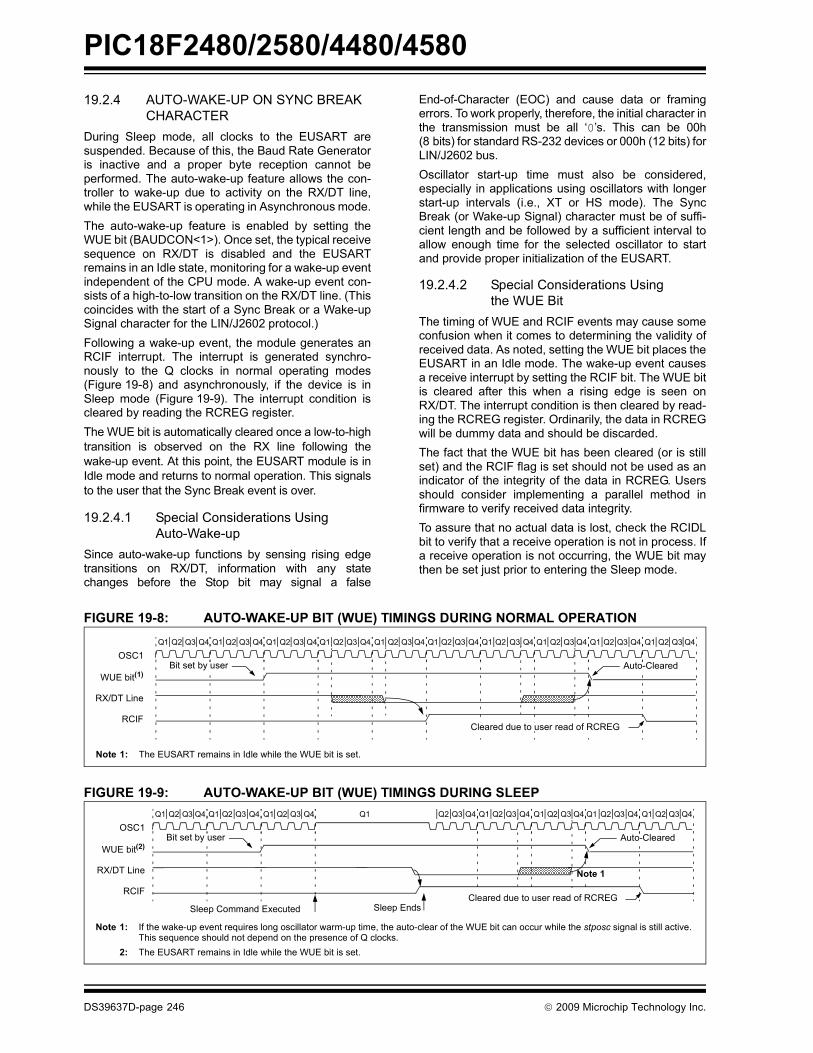
PIC18F2480/2580/4480/4580
19.2.4 AUTO-WAKE-UP ON SYNC BREAKCHARACTERDuring Sleep mode, all clocks to the EUSART aresuspended. Because of this, the Baud Rate Generatoris inactive and a proper byte reception cannot beperformed. The auto-wake-up feature allows the con-troller to wake-up due to activity on the RX/DT line,while the EUSART is operating in Asynchronous mode.The auto-wake-up feature is enabled by setting theWUE bit (BAUDCON<1>). Once set, the typical receivesequence on RX/DT is disabled and the EUSARTremains in an Idle state, monitoring for a wake-up eventindependent of the CPU mode. A wake-up event con-sists of a high-to-low transition on the RX/DT line. (Thiscoincides with the start of a Sync Break or a Wake-upSignal character for the LIN/J2602 protocol.)Following a wake-up event, the module generates anRCIF interrupt. The interrupt is generated synchro-nously to the Q clocks in normal operating modes(Figure 19-8) and asynchronously, if the device is inSleep mode (Figure 19-9). The interrupt condition iscleared by reading the RCREG register.The WUE bit is automatically cleared once a low-to-hightransition is observed on the RX line following thewake-up event. At this point, the EUSART module is inIdle mode and returns to normal operation. This signalsto the user that the Sync Break event is over.
19.2.4.1 Special Considerations Using Auto-Wake-up
Since auto-wake-up functions by sensing rising edgetransitions on RX/DT, information with any statechanges before the Stop bit may signal a false
End-of-Character (EOC) and cause data or framingerrors. To work properly, therefore, the initial character inthe transmission must be all ‘0’s. This can be 00h(8 bits) for standard RS-232 devices or 000h (12 bits) forLIN/J2602 bus.Oscillator start-up time must also be considered,especially in applications using oscillators with longerstart-up intervals (i.e., XT or HS mode). The SyncBreak (or Wake-up Signal) character must be of suffi-cient length and be followed by a sufficient interval toallow enough time for the selected oscillator to startand provide proper initialization of the EUSART.
19.2.4.2 Special Considerations Using the WUE Bit
The timing of WUE and RCIF events may cause someconfusion when it comes to determining the validity ofreceived data. As noted, setting the WUE bit places theEUSART in an Idle mode. The wake-up event causesa receive interrupt by setting the RCIF bit. The WUE bitis cleared after this when a rising edge is seen onRX/DT. The interrupt condition is then cleared by read-ing the RCREG register. Ordinarily, the data in RCREGwill be dummy data and should be discarded. The fact that the WUE bit has been cleared (or is stillset) and the RCIF flag is set should not be used as anindicator of the integrity of the data in RCREG. Usersshould consider implementing a parallel method infirmware to verify received data integrity.To assure that no actual data is lost, check the RCIDLbit to verify that a receive operation is not in process. Ifa receive operation is not occurring, the WUE bit maythen be set just prior to entering the Sleep mode.
FIGURE 19-8: AUTO-WAKE-UP BIT (WUE) TIMINGS DURING NORMAL OPERATION
FIGURE 19-9: AUTO-WAKE-UP BIT (WUE) TIMINGS DURING SLEEP
Q1 Q2 Q3 Q4 Q1 Q2 Q3 Q4 Q1 Q2 Q3 Q4 Q1 Q2 Q3 Q4 Q1 Q2 Q3 Q4 Q1 Q2 Q3 Q4 Q1 Q2 Q3 Q4 Q1 Q2 Q3 Q4 Q1 Q2 Q3 Q4 Q1 Q2 Q3 Q4
OSC1
WUE bit(1)
RX/DT Line
RCIF
Note 1: The EUSART remains in Idle while the WUE bit is set.
Bit set by user Auto-Cleared
Cleared due to user read of RCREG
Q1 Q2 Q3 Q4 Q1 Q2 Q3 Q4 Q1 Q2 Q3 Q4 Q1 Q2 Q3 Q4 Q1 Q2 Q3 Q4 Q1 Q2 Q3 Q4 Q1 Q2 Q3 Q4 Q1 Q2 Q3 Q4
OSC1
WUE bit(2)
RX/DT Line
RCIF
Sleep Command Executed
Note 1: If the wake-up event requires long oscillator warm-up time, the auto-clear of the WUE bit can occur while the stposc signal is still active.This sequence should not depend on the presence of Q clocks.
2: The EUSART remains in Idle while the WUE bit is set.
Sleep Ends
Auto-Cleared
Note 1
Cleared due to user read of RCREG
Bit set by user
DS39637D-page 246 © 2009 Microchip Technology Inc.

PIC18F2480/2580/4480/4580
19.2.5 BREAK CHARACTER SEQUENCEThe Enhanced EUSART module has the capability ofsending the special Break character sequences thatare required by the LIN/J2602 bus standard. The Breakcharacter transmit consists of a Start bit, followed bytwelve ‘0’ bits and a Stop bit. The Frame Break charac-ter is sent whenever the SENDB and TXEN bits(TXSTA<3> and TXSTA<5>) are set while the TransmitShift register is loaded with data. Note that the value ofdata written to TXREG will be ignored and all ‘0’s willbe transmitted.The SENDB bit is automatically reset by hardware afterthe corresponding Stop bit is sent. This allows the userto preload the transmit FIFO with the next transmit bytefollowing the Break character (typically, the Synccharacter in the LIN/J2602 specification).
Note that the data value written to the TXREG for theBreak character is ignored. The write simply serves thepurpose of initiating the proper sequence.
The TRMT bit indicates when the transmit operation isactive or Idle, just as it does during normal transmis-sion. See Figure 19-10 for the timing of the Breakcharacter sequence.
19.2.5.1 Break and Sync Transmit SequenceThe following sequence will send a message frameheader made up of a Break, followed by an Auto-BaudSync byte. This sequence is typical of a LIN/J2602 busmaster.
1. Configure the EUSART for the desired mode.2. Set the TXEN and SENDB bits to set up the
Break character.3. Load the TXREG with a dummy character to
initiate transmission (the value is ignored).4. Write ‘55h’ to TXREG to load the Sync character
into the transmit FIFO buffer.5. After the Break has been sent, the SENDB bit is
reset by hardware. The Sync character nowtransmits in the preconfigured mode.
When the TXREG becomes empty, as indicated by theTXIF, the next data byte can be written to TXREG.
19.2.6 RECEIVING A BREAK CHARACTERThe Enhanced USART module can receive a Breakcharacter in two ways.
The first method forces configuration of the baud rateat a frequency of 9/13 the typical speed. This allows forthe Stop bit transition to be at the correct sampling loca-tion (13 bits for Break versus Start bit and 8 data bits fortypical data).
The second method uses the auto-wake-up featuredescribed in Section 19.2.4 “Auto-Wake-up on SyncBreak Character”. By enabling this feature, theEUSART will sample the next two transitions on RX/DT,cause an RCIF interrupt and receive the next data bytefollowed by another interrupt.
Note that following a Break character, the user willtypically want to enable the Auto-Baud Rate Detectfeature. For both methods, the user can set the ABD bitonce the TXIF interrupt is observed.
FIGURE 19-10: SEND BREAK CHARACTER SEQUENCE
Write to TXREG
BRG Output(Shift Clock)
Start Bit Bit 0 Bit 1 Bit 11 Stop Bit
Break
TXIF bit(Transmit Buffer
Reg. Empty Flag)
TX (pin)
TRMT bit(Transmit Shift
Reg. Empty Flag)
SENDB(Transmit Shift
Reg. Empty Flag)
SENDB sampled here Auto-Cleared
Dummy Write
© 2009 Microchip Technology Inc. DS39637D-page 247

PIC18F2480/2580/4480/4580
19.3 EUSART SynchronousMaster ModeThe Master mode indicates that the processor trans-mits the master clock on the CK line. The SynchronousMaster mode is entered by setting the CSRC bit(TXSTA<7>). In this mode, the data is transmitted in ahalf-duplex manner (i.e., transmission and reception donot occur at the same time). When transmitting data,the reception is inhibited and vice versa. Synchronousmode is entered by setting bit, SYNC (TXSTA<4>). Inaddition, enable bit, SPEN (RCSTA<7>), is set in orderto configure the TX and RX pins to CK (clock) and DT(data) lines, respectively.
The Master mode indicates that the processor trans-mits the master clock on the CK line. Clock polarity isselected with the SCKP bit (BAUDCON<4>). SettingSCKP sets the Idle state on CK as high, while clearingthe bit sets the Idle state as low. This option is providedto support Microwire devices with this module.
19.3.1 EUSART SYNCHRONOUS MASTER TRANSMISSION
The EUSART transmitter block diagram is shown inFigure 19-3. The heart of the transmitter is the Transmit(Serial) Shift Register (TSR). The Shift register obtainsits data from the Read/Write Transmit Buffer register,TXREG. The TXREG register is loaded with data insoftware. The TSR register is not loaded until the lastbit has been transmitted from the previous load. Assoon as the last bit is transmitted, the TSR is loadedwith new data from the TXREG (if available).
Once the TXREG register transfers the data to the TSRregister (occurs in one TCYCLE), the TXREG is emptyand the TXIF flag bit (PIR1<4>) is set. The interrupt canbe enabled or disabled by setting or clearing the inter-rupt enable bit, TXIE (PIE1<4>). TXIF is set regardlessof the state of enable bit TXIE; it cannot be cleared insoftware. It will reset only when new data is loaded intothe TXREG register.
While flag bit, TXIF, indicates the status of the TXREGregister, another bit, TRMT (TXSTA<1>), shows thestatus of the TSR register. TRMT is a read-only bit whichis set when the TSR is empty. No interrupt logic is tied tothis bit so the user has to poll this bit in order todetermine if the TSR register is empty. The TSR is notmapped in data memory so it is not available to the user.
To set up a Synchronous Master Transmission:
1. Initialize the SPBRGH:SPBRG registers for theappropriate baud rate. Set or clear the BRG16bit, as required, to achieve the desired baudrate.
2. Enable the synchronous master serial port bysetting bits, SYNC, SPEN and CSRC.
3. If interrupts are desired, set enable bit, TXIE.4. If 9-bit transmission is desired, set bit, TX9.5. Enable the transmission by setting bit, TXEN.6. If 9-bit transmission is selected, the ninth bit
should be loaded in bit, TX9D.7. Start transmission by loading data to the TXREG
register.8. If using interrupts, ensure that the GIE and PEIE
bits in the INTCON register (INTCON<7:6>) areset.
FIGURE 19-11: SYNCHRONOUS TRANSMISSION
bit 0 bit 1 bit 7Word 1
Q1 Q2 Q3Q4 Q1 Q2 Q3 Q4 Q1Q2 Q3 Q4 Q1Q2 Q3 Q4Q1 Q2 Q3 Q4 Q3 Q4 Q1 Q2 Q3Q4 Q1Q2 Q3Q4 Q1 Q2Q3Q4 Q1 Q2Q3 Q4Q1 Q2 Q3 Q4 Q1 Q2 Q3 Q4
bit 2 bit 0 bit 1 bit 7RC7/RX/DT
RC6/TX/CK pin
Write toTXREG Reg
TXIF bit(Interrupt Flag)
TXEN bit ‘1’ ‘1’
Word 2
TRMT bit
Write Word 1 Write Word 2
Note: Sync Master mode, SPBRG = 0, continuous transmission of two 8-bit words.
pin
RC6/TX/CK pin(SCKP = 0)
(SCKP = 1)
DS39637D-page 248 © 2009 Microchip Technology Inc.

PIC18F2480/2580/4480/4580
FIGURE 19-12: SYNCHRONOUS TRANSMISSION (THROUGH TXEN)TABLE 19-7: REGISTERS ASSOCIATED WITH SYNCHRONOUS MASTER TRANSMISSION
Name Bit 7 Bit 6 Bit 5 Bit 4 Bit 3 Bit 2 Bit 1 Bit 0Reset Values
on Page:
INTCON GIE/GIEH PEIE/GIEL TMR0IE INT0IE RBIE TMR0IF INT0IF RBIF 55PIR1 PSPIF(1) ADIF RCIF TXIF SSPIF CCP1IF TMR2IF TMR1IF 58PIE1 PSPIE(1) ADIE RCIE TXIE SSPIE CCP1IE TMR2IE TMR1IE 58IPR1 PSPIP(1) ADIP RCIP TXIP SSPIP CCP1IP TMR2IP TMR1IP 58RCSTA SPEN RX9 SREN CREN ADDEN FERR OERR RX9D 57TXREG EUSART Transmit Register 57TXSTA CSRC TX9 TXEN SYNC SENDB BRGH TRMT TX9D 57BAUDCON ABDOVF RCIDL — SCKP BRG16 — WUE ABDEN 57SPBRGH EUSART Baud Rate Generator Register, High Byte 57SPBRG EUSART Baud Rate Generator Register, Low Byte 57Legend: — = unimplemented, read as ‘0’. Shaded cells are not used for synchronous master transmission.Note 1: Reserved in PIC18F2X80 devices; always maintain these bits clear.
RC7/RX/DT pin
RC6/TX/CK pin
Write toTXREG reg
TXIF bit
TRMT bit
bit 0 bit 1 bit 2 bit 6 bit 7
TXEN bit
© 2009 Microchip Technology Inc. DS39637D-page 249

PIC18F2480/2580/4480/4580
19.3.2 EUSART SYNCHRONOUSMASTER RECEPTIONOnce Synchronous mode is selected, reception isenabled by setting either the Single Receive Enable bit,SREN (RCSTA<5>), or the Continuous ReceiveEnable bit, CREN (RCSTA<4>). Data is sampled on theRX pin on the falling edge of the clock.If enable bit, SREN, is set, only a single word isreceived. If enable bit, CREN, is set, the reception iscontinuous until CREN is cleared. If both bits are set,then CREN takes precedence.To set up a Synchronous Master Reception:1. Initialize the SPBRGH:SPBRG registers for the
appropriate baud rate. Set or clear the BRG16bit, as required, to achieve the desired baud rate.
2. Enable the synchronous master serial port bysetting bits, SYNC, SPEN and CSRC.
3. Ensure bits, CREN and SREN, are clear.4. If interrupts are desired, set enable bit, RCIE.5. If 9-bit reception is desired, set bit, RX9.6. If a single reception is required, set bit, SREN.
For continuous reception, set bit, CREN.7. Interrupt flag bit, RCIF, will be set when
reception is complete and an interrupt will begenerated if the enable bit, RCIE, was set.
8. Read the RCSTA register to get the 9th bit (ifenabled) and determine if any error occurredduring reception.
9. Read the 8-bit received data by reading theRCREG register.
10. If any error occurred, clear the error by clearingbit, CREN.
11. If using interrupts, ensure that the GIE and PEIEbits in the INTCON register (INTCON<7:6>) areset.
FIGURE 19-13: SYNCHRONOUS RECEPTION (MASTER MODE, SREN)
TABLE 19-8: REGISTERS ASSOCIATED WITH SYNCHRONOUS MASTER RECEPTION
Name Bit 7 Bit 6 Bit 5 Bit 4 Bit 3 Bit 2 Bit 1 Bit 0Reset
Values on Page:
INTCON GIE/GIEH PEIE/GIEL TMR0IE INT0IE RBIE TMR0IF INT0IF RBIF 55PIR1 PSPIF(1) ADIF RCIF TXIF SSPIF CCP1IF TMR2IF TMR1IF 58PIE1 PSPIE(1) ADIE RCIE TXIE SSPIE CCP1IE TMR2IE TMR1IE 58IPR1 PSPIP(1) ADIP RCIP TXIP SSPIP CCP1IP TMR2IP TMR1IP 58RCSTA SPEN RX9 SREN CREN ADDEN FERR OERR RX9D 57RCREG EUSART Receive Register 57TXSTA CSRC TX9 TXEN SYNC SENDB BRGH TRMT TX9D 57BAUDCON ABDOVF RCIDL — SCKP BRG16 — WUE ABDEN 57SPBRGH EUSART Baud Rate Generator Register High Byte 57SPBRG EUSART Baud Rate Generator Register Low Byte 57Legend: — = unimplemented, read as ‘0’. Shaded cells are not used for synchronous master reception.Note 1: Reserved in PIC18F2X80 devices; always maintain these bits clear.
CREN bit
RC7/RX1/DT1
RC7/TX/CK pin
Write tobit SREN
SREN bit
RCIF bit(Interrupt)
ReadRXREG
Q3 Q4 Q1 Q2 Q3 Q4 Q1 Q2 Q3 Q4Q2 Q1 Q2 Q3 Q4 Q1 Q2 Q3 Q4 Q1 Q2 Q3 Q4 Q1 Q2 Q3 Q4 Q1Q2 Q3 Q4 Q1 Q2 Q3 Q4 Q1 Q2 Q3 Q4
‘0’
bit 0 bit 1 bit 2 bit 3 bit 4 bit 5 bit 6 bit 7
‘0’
Q1 Q2 Q3 Q4
Note: Timing diagram demonstrates Sync Master mode with bit, SREN = 1, and bit, BRGH = 0.
RC7/TX/CK pin
pin
(SCKP = 0)
(SCKP = 1)
DS39637D-page 250 © 2009 Microchip Technology Inc.

PIC18F2480/2580/4480/4580
19.4 EUSART SynchronousSlave ModeSynchronous Slave mode is entered by clearing bitCSRC (TXSTA<7>). This mode differs from theSynchronous Master mode in that the shift clock is sup-plied externally at the CK pin (instead of being suppliedinternally in Master mode). This allows the device totransfer or receive data while in any low-power mode.
19.4.1 EUSART SYNCHRONOUS SLAVE TRANSMIT
The operation of the Synchronous Master and Slavemodes are identical, except in the case of the Sleepmode.
If two words are written to the TXREG and then theSLEEP instruction is executed, the following will occur:
a) The first word will immediately transfer to theTSR register and transmit.
b) The second word will remain in the TXREGregister.
c) Flag bit, TXIF, will not be set. d) When the first word has been shifted out of TSR,
the TXREG register will transfer the secondword to the TSR and flag bit, TXIF, will now beset.
e) If enable bit, TXIE, is set, the interrupt will wakethe chip from Sleep. If the global interrupt isenabled, the program will branch to the interruptvector.
To set up a Synchronous Slave Transmission:
1. Enable the synchronous slave serial port bysetting bits, SYNC and SPEN, and clearing bit,CSRC.
2. Clear bits, CREN and SREN.3. If interrupts are desired, set enable bit, TXIE.4. If 9-bit transmission is desired, set bit, TX9.5. Enable the transmission by setting enable bit,
TXEN.6. If 9-bit transmission is selected, the ninth bit
should be loaded in bit, TX9D.7. Start transmission by loading data to the
TXREGx register.8. If using interrupts, ensure that the GIE and PEIE
bits in the INTCON register (INTCON<7:6>) areset.
TABLE 19-9: REGISTERS ASSOCIATED WITH SYNCHRONOUS SLAVE TRANSMISSION
Name Bit 7 Bit 6 Bit 5 Bit 4 Bit 3 Bit 2 Bit 1 Bit 0Reset Values
on Page:
INTCON GIE/GIEH PEIE/GIEL TMR0IE INT0IE RBIE TMR0IF INT0IF RBIF 55PIR1 PSPIF(1) ADIF RCIF TXIF SSPIF CCP1IF TMR2IF TMR1IF 58PIE1 PSPIE(1) ADIE RCIE TXIE SSPIE CCP1IE TMR2IE TMR1IE 58IPR1 PSPIP(1) ADIP RCIP TXIP SSPIP CCP1IP TMR2IP TMR1IP 58RCSTA SPEN RX9 SREN CREN ADDEN FERR OERR RX9D 57TXREG EUSART Transmit Register 57TXSTA CSRC TX9 TXEN SYNC SENDB BRGH TRMT TX9D 57BAUDCON ABDOVF RCIDL — SCKP BRG16 — WUE ABDEN 57SPBRGH EUSART Baud Rate Generator Register High Byte 57SPBRG EUSART Baud Rate Generator Register Low Byte 57Legend: — = unimplemented, read as ‘0’. Shaded cells are not used for synchronous slave transmission.Note 1: Reserved in PIC18F2X80 devices; always maintain these bits clear.
© 2009 Microchip Technology Inc. DS39637D-page 251

PIC18F2480/2580/4480/4580
19.4.2 EUSART SYNCHRONOUS SLAVERECEPTIONThe operation of the Synchronous Master and Slavemodes is identical, except in the case of Sleep or anyIdle mode and bit, SREN, which is a “don’t care” inSlave mode.
If receive is enabled by setting the CREN bit prior toentering Sleep or any Idle mode, then a word may bereceived while in this low-power mode. Once the wordis received, the RSR register will transfer the data to theRCREG register. If the RCIE enable bit is set, the inter-rupt generated will wake the chip from the low-powermode. If the global interrupt is enabled, the program willbranch to the interrupt vector.
To set up a Synchronous Slave Reception:
1. Enable the synchronous master serial port bysetting bits, SYNC and SPEN, and clearing bit,CSRC.
2. If interrupts are desired, set enable bit, RCIE.3. If 9-bit reception is desired, set bit, RX9.4. To enable reception, set enable bit, CREN.5. Flag bit, RCIF, will be set when reception is
complete. An interrupt will be generated ifenable bit, RCIE, was set.
6. Read the RCSTA register to get the 9th bit (ifenabled) and determine if any error occurredduring reception.
7. Read the 8-bit received data by reading theRCREG register.
8. If any error occurred, clear the error by clearingbit, CREN.
9. If using interrupts, ensure that the GIE and PEIEbits in the INTCON register (INTCON<7:6>) areset.
TABLE 19-10: REGISTERS ASSOCIATED WITH SYNCHRONOUS SLAVE RECEPTION
Name Bit 7 Bit 6 Bit 5 Bit 4 Bit 3 Bit 2 Bit 1 Bit 0Reset Values
on Page:
INTCON GIE/GIEH PEIE/GIEL TMR0IE INT0IE RBIE TMR0IF INT0IF RBIF 55PIR1 PSPIF(1) ADIF RCIF TXIF SSPIF CCP1IF TMR2IF TMR1IF 58PIE1 PSPIE(1) ADIE RCIE TXIE SSPIE CCP1IE TMR2IE TMR1IE 58IPR1 PSPIP(1) ADIP RCIP TXIP SSPIP CCP1IP TMR2IP TMR1IP 58RCSTA SPEN RX9 SREN CREN ADDEN FERR OERR RX9D 57RCREG EUSART Receive Register 57TXSTA CSRC TX9 TXEN SYNC SENDB BRGH TRMT TX9D 57BAUDCON ABDOVF RCIDL — SCKP BRG16 — WUE ABDEN 57SPBRGH EUSART Baud Rate Generator Register High Byte 57SPBRG EUSART Baud Rate Generator Register Low Byte 57Legend: — = unimplemented, read as ‘0’. Shaded cells are not used for synchronous slave reception.Note 1: Reserved in PIC18F2X80 devices; always maintain these bits clear.
DS39637D-page 252 © 2009 Microchip Technology Inc.

PIC18F2480/2580/4480/4580
20.0 10-BIT ANALOG-TO-DIGITAL CONVERTER (A/D) MODULE
The Analog-to-Digital (A/D) Converter module has8 inputs for the PIC18F2X80 devices and 11 for thePIC18F4X80 devices. This module allows conversionof an analog input signal to a corresponding 10-bitdigital number.
The module has five registers:
• A/D Result High Register (ADRESH)• A/D Result Low Register (ADRESL)• A/D Control Register 0 (ADCON0)• A/D Control Register 1 (ADCON1)• A/D Control Register 2 (ADCON2)
The ADCON0 register, shown in Register 20-1,controls the operation of the A/D module. TheADCON1 register, shown in Register 20-2, configuresthe functions of the port pins. The ADCON2 register,shown in Register 20-3, configures the A/D clocksource, programmed acquisition time and justification.
REGISTER 20-1: ADCON0: A/D CONTROL REGISTER 0
U-0 U-0 R/W-0 R/W-0 R/W-0 R/W-0 R/W-0 R/W-0
— — CHS3 CHS2 CHS1 CHS0 GO/DONE ADONbit 7 bit 0
Legend:R = Readable bit W = Writable bit U = Unimplemented bit, read as ‘0’-n = Value at POR ‘1’ = Bit is set ‘0’ = Bit is cleared x = Bit is unknown
bit 7-6 Unimplemented: Read as ‘0’bit 5-2 CHS<3:0>: Analog Channel Select bits
0000 = Channel 0 (AN0)0001 = Channel 1 (AN1)0010 = Channel 2 (AN2)0011 = Channel 3 (AN3)0100 = Channel 4 (AN4)0101 = Channel 5 (AN5)(1,2) 0110 = Channel 6 (AN6)(1,2) 0111 = Channel 7 (AN7)(1,2)
1000 = Channel 8 (AN8)1001 = Channel 9 (AN9)1010 = Channel 10 (AN10)1011 = Unused1100 = Unused1101 = Unused1110 = Unused1111 = Unused
bit 1 GO/DONE: A/D Conversion Status bitWhen ADON = 1: 1 = A/D conversion in progress0 = A/D Idle
bit 0 ADON: A/D On bit1 = A/D Converter module is enabled 0 = A/D Converter module is disabled
Note 1: These channels are not implemented on PIC18F2X80 devices.2: Performing a conversion on unimplemented channels will return full-scale measurements.
© 2009 Microchip Technology Inc. DS39637D-page 253
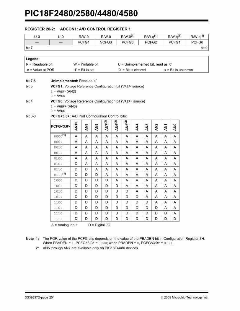
PIC18F2480/2580/4480/4580
REGISTER 20-2: ADCON1: A/D CONTROL REGISTER 1U-0 U-0 R/W-0 R/W-0 R/W-0(1) R/W-q(1) R/W-q(1) R/W-q(1)
— — VCFG1 VCFG0 PCFG3 PCFG2 PCFG1 PCFG0bit 7 bit 0
Legend:R = Readable bit W = Writable bit U = Unimplemented bit, read as ‘0’-n = Value at POR ‘1’ = Bit is set ‘0’ = Bit is cleared x = Bit is unknown
bit 7-6 Unimplemented: Read as ‘0’bit 5 VCFG1: Voltage Reference Configuration bit (VREF- source)
1 = VREF- (AN2)0 = AVSS
bit 4 VCFG0: Voltage Reference Configuration bit (VREF+ source)1 = VREF+ (AN3)0 = AVDD
bit 3-0 PCFG<3:0>: A/D Port Configuration Control bits:
Note 1: The POR value of the PCFG bits depends on the value of the PBADEN bit in Configuration Register 3H. When PBADEN = 1, PCFG<3:0> = 0000; when PBADEN = 0, PCFG<3:0> = 0111.
2: AN5 through AN7 are available only on PIC18F4X80 devices.
A = Analog input D = Digital I/O
PCFG<3:0>
AN
10
AN
9
AN
8
AN
7(2)
AN
6(2)
AN
5(2)
AN
4
AN
3
AN
2
AN
1
AN
0
0000(1) A A A A A A A A A A A0001 A A A A A A A A A A A0010 A A A A A A A A A A A0011 A A A A A A A A A A A0100 A A A A A A A A A A A0101 D A A A A A A A A A A0110 D D A A A A A A A A A0111(1) D D D A A A A A A A A1000 D D D D A A A A A A A1001 D D D D D A A A A A A1010 D D D D D D A A A A A1011 D D D D D D D A A A A1100 D D D D D D D D A A A1101 D D D D D D D D D A A1110 D D D D D D D D D D A1111 D D D D D D D D D D D
DS39637D-page 254 © 2009 Microchip Technology Inc.

PIC18F2480/2580/4480/4580
REGISTER 20-3: ADCON2: A/D CONTROL REGISTER 2R/W-0 U-0 R/W-0 R/W-0 R/W-0 R/W-0 R/W-0 R/W-0ADFM — ACQT2 ACQT1 ACQT0 ADCS2 ADCS1 ADCS0
bit 7 bit 0
Legend:R = Readable bit W = Writable bit U = Unimplemented bit, read as ‘0’-n = Value at POR ‘1’ = Bit is set ‘0’ = Bit is cleared x = Bit is unknown
bit 7 ADFM: A/D Result Format Select bit1 = Right justified 0 = Left justified
bit 6 Unimplemented: Read as ‘0’bit 5-3 ACQT<2:0>: A/D Acquisition Time Select bits
111 = 20 TAD110 = 16 TAD101 = 12 TAD100 = 8 TAD011 = 6 TAD010 = 4 TAD001 = 2 TAD000 = 0 TAD(1)
bit 2-0 ADCS<2:0>: A/D Conversion Clock Select bits111 = FRC (clock derived from A/D RC oscillator)(1) 110 = FOSC/64 101 = FOSC/16 100 = FOSC/4 011 = FRC (clock derived from A/D RC oscillator)(1) 010 = FOSC/32 001 = FOSC/8 000 = FOSC/2
Note 1: If the A/D FRC clock source is selected, a delay of one TCY (instruction cycle) is added before the A/D clock starts. This allows the SLEEP instruction to be executed before starting a conversion.
© 2009 Microchip Technology Inc. DS39637D-page 255

PIC18F2480/2580/4480/4580
The analog reference voltage is software-selectable toeither the device’s positive and negative supply voltage(AVDD and AVSS), or the voltage level on theRA3/AN3/VREF+ and RA2/AN2/VREF-/CVREF pins.The A/D Converter has a unique feature of being ableto operate while the device is in Sleep mode. To oper-ate in Sleep, the A/D conversion clock must be derivedfrom the A/D’s internal RC oscillator.
The output of the sample and hold is the input into theconverter, which generates the result via successiveapproximation.
A device Reset forces all registers to their Reset state.This forces the A/D module to be turned off and anyconversion in progress is aborted.
Each port pin associated with the A/D Converter can beconfigured as an analog input, or as a digital I/O. TheADRESH and ADRESL registers contain the result ofthe A/D conversion. When the A/D conversion is com-plete, the result is loaded into the ADRESH/ADRESLregisters, the GO/DONE bit (ADCON0 register) iscleared and A/D Interrupt Flag bit, ADIF, is set. Theblock diagram of the A/D module is shown inFigure 20-1.
FIGURE 20-1: A/D BLOCK DIAGRAM
(Input Voltage)VAIN
VREF+ReferenceVoltage
AVDD(2)
VCFG<1:0>
CHS<3:0>
AN7(1)
AN6(1)
AN5(1)
AN4
AN3
AN2
AN1
AN0
0111
0110
0101
0100
0011
0010
0001
0000
10-BitA/D
VREF-
AVSS(2)
Converter
AN10
AN9
AN8
1010
1001
1000
Note 1: Channels, AN5 through AN7, are not available on PIC18F2X80 devices.2: I/O pins have diode protection to VDD and VSS.
0X1XX1X0
DS39637D-page 256 © 2009 Microchip Technology Inc.

PIC18F2480/2580/4480/4580
The value in the ADRESH/ADRESL registers is notmodified for a Power-on Reset. The ADRESH/ADRESLregisters will contain unknown data after a Power-onReset.After the A/D module has been configured as desired,the selected channel must be acquired before the con-version is started. The analog input channels musthave their corresponding TRIS bits selected as aninput. To determine acquisition time, see Section 20.1“A/D Acquisition Requirements”. After this acquisi-tion time has elapsed, the A/D conversion can bestarted. An acquisition time can be programmed tooccur between setting the GO/DONE bit and the actualstart of the conversion.
The following steps should be followed to perform anA/D conversion:
1. Configure the A/D module:• Configure analog pins, voltage reference and
digital I/O (ADCON1)• Select A/D input channel (ADCON0)• Select A/D acquisition time (ADCON2)• Select A/D conversion clock (ADCON2)• Turn on A/D module (ADCON0)
2. Configure A/D interrupt (if desired):• Clear ADIF bit • Set ADIE bit • Set GIE bit
3. Wait the required acquisition time (if required).4. Start conversion:
• Set GO/DONE bit (ADCON0 register)5. Wait for A/D conversion to complete, by either:
• Polling for the GO/DONE bit to be cleared
OR
• Waiting for the A/D interrupt6. Read A/D Result registers (ADRESH:ADRESL);
clear bit, ADIF, if required.7. For next conversion, go to step 1 or step 2, as
required. The A/D conversion time per bit isdefined as TAD. A minimum wait of 2 TAD isrequired before next acquisition starts.
FIGURE 20-2: ANALOG INPUT MODEL
VAIN CPIN
Rs ANx
5 pF
VDD
VT = 0.6V
VT = 0.6VILEAKAGE
RIC ≤ 1k
SamplingSwitch
SS RSS
CHOLD = 120 pF
VSS
6V
Sampling Switch
5V4V3V2V
5 6 7 8 9 10 11(kΩ)
VDD
± 100 nA
Legend: CPIN
VTILEAKAGE
RIC
SSCHOLD
= Input Capacitance= Threshold Voltage= Leakage Current at the pin due to
= Interconnect Resistance= Sampling Switch= Sample/Hold Capacitance (from DAC)
various junctions
= Sampling Switch ResistanceRSS
© 2009 Microchip Technology Inc. DS39637D-page 257
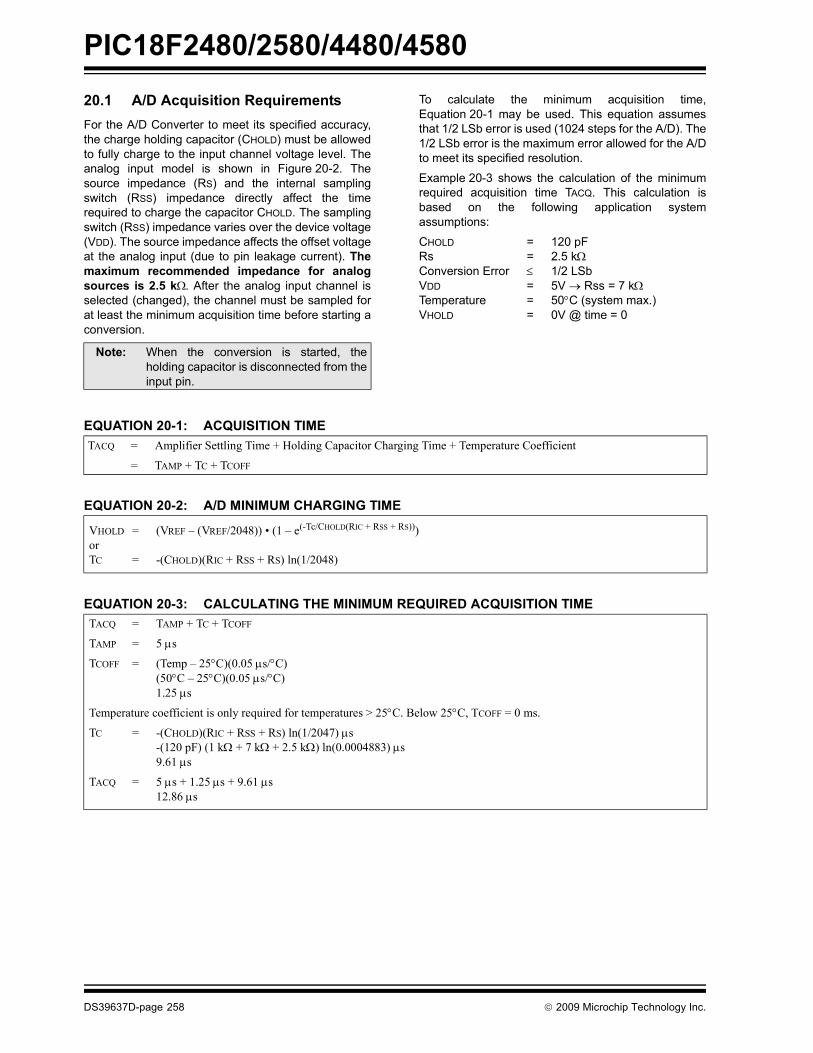
PIC18F2480/2580/4480/4580
20.1 A/D Acquisition RequirementsFor the A/D Converter to meet its specified accuracy,the charge holding capacitor (CHOLD) must be allowedto fully charge to the input channel voltage level. Theanalog input model is shown in Figure 20-2. Thesource impedance (RS) and the internal samplingswitch (RSS) impedance directly affect the timerequired to charge the capacitor CHOLD. The samplingswitch (RSS) impedance varies over the device voltage(VDD). The source impedance affects the offset voltageat the analog input (due to pin leakage current). Themaximum recommended impedance for analogsources is 2.5 kΩ. After the analog input channel isselected (changed), the channel must be sampled forat least the minimum acquisition time before starting aconversion.To calculate the minimum acquisition time,Equation 20-1 may be used. This equation assumesthat 1/2 LSb error is used (1024 steps for the A/D). The1/2 LSb error is the maximum error allowed for the A/Dto meet its specified resolution.
Example 20-3 shows the calculation of the minimumrequired acquisition time TACQ. This calculation isbased on the following application systemassumptions:
CHOLD = 120 pF Rs = 2.5 kΩ Conversion Error ≤ 1/2 LSb VDD = 5V → Rss = 7 kΩ Temperature = 50°C (system max.) VHOLD = 0V @ time = 0
EQUATION 20-1: ACQUISITION TIME
EQUATION 20-2: A/D MINIMUM CHARGING TIME
EQUATION 20-3: CALCULATING THE MINIMUM REQUIRED ACQUISITION TIME
Note: When the conversion is started, theholding capacitor is disconnected from theinput pin.
TACQ = Amplifier Settling Time + Holding Capacitor Charging Time + Temperature Coefficient
= TAMP + TC + TCOFF
VHOLD = (VREF – (VREF/2048)) • (1 – e(-Tc/CHOLD(RIC + RSS + RS))) or TC = -(CHOLD)(RIC + RSS + RS) ln(1/2048)
TACQ = TAMP + TC + TCOFF
TAMP = 5 μs
TCOFF = (Temp – 25°C)(0.05 μs/°C)(50°C – 25°C)(0.05 μs/°C)1.25 μs
Temperature coefficient is only required for temperatures > 25°C. Below 25°C, TCOFF = 0 ms.
TC = -(CHOLD)(RIC + RSS + RS) ln(1/2047) μs-(120 pF) (1 kΩ + 7 kΩ + 2.5 kΩ) ln(0.0004883) μs 9.61 μs
TACQ = 5 μs + 1.25 μs + 9.61 μs12.86 μs
DS39637D-page 258 © 2009 Microchip Technology Inc.

PIC18F2480/2580/4480/4580
20.2 Selecting and ConfiguringAutomatic Acquisition TimeThe ADCON2 register allows the user to select anacquisition time that occurs each time the GO/DONEbit is set.
When the GO/DONE bit is set, sampling is stopped anda conversion begins. The user is responsible for ensur-ing the required acquisition time has passed betweenselecting the desired input channel and setting theGO/DONE bit. This occurs when the ACQT<2:0> bits(ADCON2<5:3>) remain in their Reset state (‘000’) andis compatible with devices that do not offerprogrammable acquisition times.
If desired, the ACQT bits can be set to select aprogrammable acquisition time for the A/D module.When the GO/DONE bit is set, the A/D modulecontinues to sample the input for the selected acquisitiontime, then automatically begins a conversion. Since theacquisition time is programmed, there may be no needto wait for an acquisition time between selecting achannel and setting the GO/DONE bit.
In either case, when the conversion is completed, theGO/DONE bit is cleared, the ADIF flag is set and theA/D begins sampling the currently selected channelagain. If an acquisition time is programmed, there isnothing to indicate if the acquisition time has ended orif the conversion has begun.
20.3 Selecting the A/D Conversion Clock
The A/D conversion time per bit is defined as TAD. TheA/D conversion requires 11 TAD per 10-bit conversion.The source of the A/D conversion clock issoftware-selectable. There are seven possible optionsfor TAD:
• 2 TOSC
• 4 TOSC
• 8 TOSC
• 16 TOSC
• 32 TOSC • 64 TOSC
• Internal RC Oscillator
For correct A/D conversions, the A/D conversion clock(TAD) must be as short as possible, but greater than theminimum TAD (approximately 2 μs, see parameter 130for more information).
Table 20-1 shows the resultant TAD times derived fromthe device operating frequencies and the A/D clocksource selected.
TABLE 20-1: TAD vs. DEVICE OPERATING FREQUENCIES AD Clock Source (TAD) Maximum Device Frequency
Operation ADCS2:ADCS0 PIC18F2X80/4X80 PIC18LF2X80/4X80(4)
2 TOSC 000 2.86 MHz 1.43 kHz4 TOSC 100 5.71 MHz 2.86 MHz8 TOSC 001 11.43 MHz 5.72 MHz
16 TOSC 101 22.86 MHz 11.43 MHz32 TOSC 010 40.0 MHz 22.86 MHz64 TOSC 110 40.0 MHz 22.86 MHz
RC(3) x11 1.00 MHz(1) 1.00 MHz(2)
Note 1: The RC source has a typical TAD time of 1.2 ms.2: The RC source has a typical TAD time of 2.5 ms.3: For device frequencies above 1 MHz, the device must be in Sleep for the entire conversion or the A/D
accuracy may be out of specification.4: Low-power (PIC18LFXXXX) devices only.
© 2009 Microchip Technology Inc. DS39637D-page 259
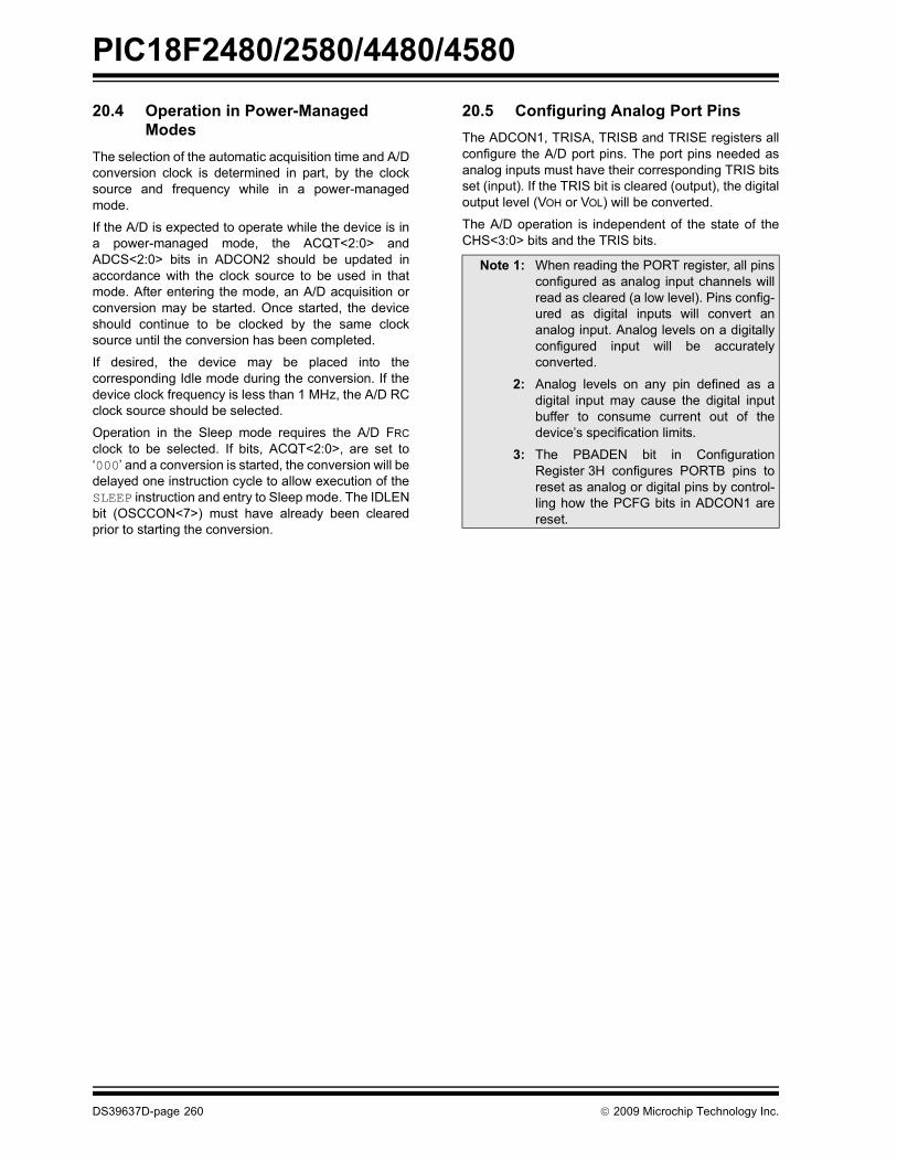
PIC18F2480/2580/4480/4580
20.4 Operation in Power-ManagedModesThe selection of the automatic acquisition time and A/Dconversion clock is determined in part, by the clocksource and frequency while in a power-managedmode.
If the A/D is expected to operate while the device is ina power-managed mode, the ACQT<2:0> andADCS<2:0> bits in ADCON2 should be updated inaccordance with the clock source to be used in thatmode. After entering the mode, an A/D acquisition orconversion may be started. Once started, the deviceshould continue to be clocked by the same clocksource until the conversion has been completed.
If desired, the device may be placed into thecorresponding Idle mode during the conversion. If thedevice clock frequency is less than 1 MHz, the A/D RCclock source should be selected.
Operation in the Sleep mode requires the A/D FRCclock to be selected. If bits, ACQT<2:0>, are set to‘000’ and a conversion is started, the conversion will bedelayed one instruction cycle to allow execution of theSLEEP instruction and entry to Sleep mode. The IDLENbit (OSCCON<7>) must have already been clearedprior to starting the conversion.
20.5 Configuring Analog Port PinsThe ADCON1, TRISA, TRISB and TRISE registers allconfigure the A/D port pins. The port pins needed asanalog inputs must have their corresponding TRIS bitsset (input). If the TRIS bit is cleared (output), the digitaloutput level (VOH or VOL) will be converted.
The A/D operation is independent of the state of theCHS<3:0> bits and the TRIS bits.
Note 1: When reading the PORT register, all pinsconfigured as analog input channels willread as cleared (a low level). Pins config-ured as digital inputs will convert ananalog input. Analog levels on a digitallyconfigured input will be accuratelyconverted.
2: Analog levels on any pin defined as adigital input may cause the digital inputbuffer to consume current out of thedevice’s specification limits.
3: The PBADEN bit in ConfigurationRegister 3H configures PORTB pins toreset as analog or digital pins by control-ling how the PCFG bits in ADCON1 arereset.
DS39637D-page 260 © 2009 Microchip Technology Inc.

PIC18F2480/2580/4480/4580
20.6 A/D Conversions Figure 20-3 shows the operation of the A/D Converterafter the GO/DONE bit has been set and theACQT<2:0> bits are cleared. A conversion is startedafter the following instruction to allow entry into Sleepmode before the conversion begins.Figure 20-4 shows the operation of the A/D Converterafter the GO/DONE bit has been set and theACQT<2:0> bits are set to ‘010’ and selecting a 4 TADacquisition time before the conversion starts.
Clearing the GO/DONE bit during a conversion willabort the current conversion. The A/D Result registerpair will NOT be updated with the partially completedA/D conversion sample. This means theADRESH:ADRESL registers will continue to containthe value of the last completed conversion (or the lastvalue written to the ADRESH:ADRESL registers).
After the A/D conversion is completed or aborted, a2 TAD wait is required before the next acquisition canbe started. After this wait, acquisition on the selectedchannel is automatically started.
FIGURE 20-3: A/D CONVERSION TAD CYCLES (ACQT<2:0> = 000, TACQ = 0)
FIGURE 20-4: A/D CONVERSION TAD CYCLES (ACQT<2:0> = 010, TACQ = 4 TAD)
Note: The GO/DONE bit should NOT be set inthe same instruction that turns on the A/D.
TAD1 TAD2 TAD3 TAD4 TAD5 TAD6 TAD7 TAD8 TAD11
Set GO/DONE bit
Holding capacitor is disconnected from analog input (typically 100 ns)
TAD9 TAD10TCY - TAD
ADRESH:ADRESL is loaded, GO/DONE bit is cleared, ADIF bit is set, holding capacitor is connected to analog input.
Conversion starts
b0b9 b6 b5 b4 b3 b2 b1b8 b7
On the following cycle:
1 2 3 4 5 6 7 8 11
Set GO/DONE bit
(Holding capacitor is disconnected)
9 10
Conversion starts
1 2 3 4
(Holding capacitor continuesacquiring input)
TACQT Cycles TAD Cycles
AutomaticAcquisition
Time
b0b9 b6 b5 b4 b3 b2 b1b8 b7
ADRESH:ADRESL is loaded, GO/DONE bit is cleared, ADIF bit is set, holding capacitor is connected to analog input.
On the following cycle:
© 2009 Microchip Technology Inc. DS39637D-page 261

PIC18F2480/2580/4480/4580
20.7 Use of the CCP1 TriggerAn A/D conversion can be started by the “Special EventTrigger” of the ECCP1 module. This requires that theECCP1M<3:0> bits (ECCP1CON<3:0>) be pro-grammed as ‘1011’ and that the A/D module is enabled(ADON bit is set). When the trigger occurs, theGO/DONE bit will be set, starting the A/D acquisitionand conversion and the Timer1 (or Timer3) counter willbe reset to zero. Timer1 (or Timer3) is reset to automat-ically repeat the A/D acquisition period with minimalsoftware overhead (moving ADRESH/ADRESL to thedesired location). The appropriate analog input chan-nel must be selected and the minimum acquisitionperiod is either timed by the user, or an appropriateTACQ time selected before the “Special Event Trigger”sets the GO/DONE bit (starts a conversion).
If the A/D module is not enabled (ADON is cleared), the“Special Event Trigger” will be ignored by the A/Dmodule, but will still reset the Timer1 (or Timer3) coun-ter.
TABLE 20-2: REGISTERS ASSOCIATED WITH A/D OPERATION
Name Bit 7 Bit 6 Bit 5 Bit 4 Bit 3 Bit 2 Bit 1 Bit 0Reset Values
on Page:
INTCON GIE/GIEH PEIE/GIEL TMR0IE INT0IE RBIE TMR0IF INT0IF RBIF 55IPR1 PSPIP ADIP RCIP TXIP SSPIP CCP1IP TMR2IP TMR1IP 58PIR1 PSPIF ADIF RCIF TXIF SSPIF CCP1IF TMR2IF TMR1IF 58PIE1 PSPIE ADIE RCIE TXIE SSPIE CCP1IE TMR2IE TMR1IE 58IPR2 OSCFIP CMIP — EEIP BCLIP HLVDIP TMR3IP ECCP1IP(5) 57PIR2 OSCFIF CMIF — EEIF BCLIF HLVDIF TMR3IF ECCP1IF(5) 58PIE2 OSCFIE CMIE — EEIE BCLIE HLVDIE TMR3IE ECCP1IE(5) 58ADRESH A/D Result Register High Byte 56ADRESL A/D Result Register Low Byte 56
ADCON0 — — CHS3 CHS2 CHS1 CHS0 GO/DONE ADON 56ADCON1 — — VCFG1 VCFG0 PCFG3 PCFG2 PCFG1 PCFG0 56ADCON2 ADFM — ACQT2 ACQT1 ACQT0 ADCS2 ADCS1 ADCS0 57PORTA RA7(2) RA6(2) RA5 RA4 RA3 RA2 RA1 RA0 58TRISA TRISA7(2) TRISA6(2) PORTA Data Direction Register 58PORTB Read PORTB pins, Write LATB Latch 58TRISB PORTB Data Direction Register 58LATB PORTB Output Data Latch 58PORTE(4) — — — — RE3(3) Read PORTE pins, Write LATE(1) 58TRISE(4) IBF OBF IBOV PSPMODE — PORTE Data Direction 58LATE(4) — — — — — LATE2 LATE1 LATE0 58Legend: — = unimplemented, read as ‘0’. Shaded cells are not used for A/D conversion.Note 1: These bits are unimplemented on PIC18F2X80 devices; always maintain these bits clear.
2: These pins may be configured as port pins depending on the Oscillator mode selected.3: RE3 port bit is available only as an input pin when the MCLRE Configuration bit is ‘0’.4: These registers are not implemented on PIC18F2X80 devices.5: These bits are available on PIC18F4X80 and reserved on PIC18F2X80 devices.
DS39637D-page 262 © 2009 Microchip Technology Inc.
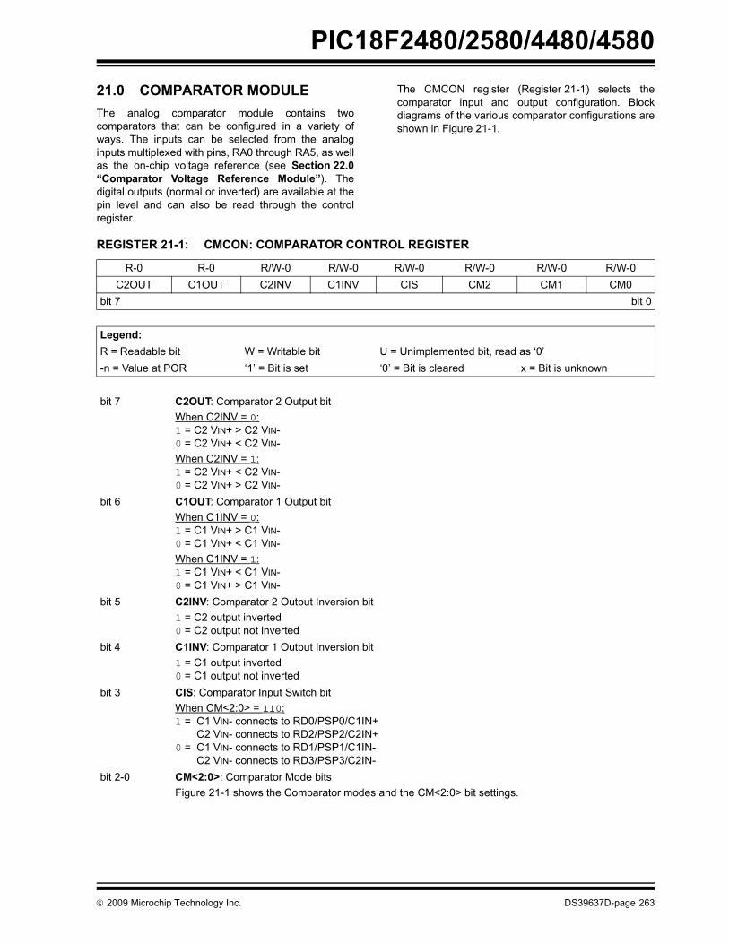
PIC18F2480/2580/4480/4580
21.0 COMPARATOR MODULEThe analog comparator module contains twocomparators that can be configured in a variety ofways. The inputs can be selected from the analoginputs multiplexed with pins, RA0 through RA5, as wellas the on-chip voltage reference (see Section 22.0“Comparator Voltage Reference Module”). Thedigital outputs (normal or inverted) are available at thepin level and can also be read through the controlregister.
The CMCON register (Register 21-1) selects thecomparator input and output configuration. Blockdiagrams of the various comparator configurations areshown in Figure 21-1.
REGISTER 21-1: CMCON: COMPARATOR CONTROL REGISTER
R-0 R-0 R/W-0 R/W-0 R/W-0 R/W-0 R/W-0 R/W-0C2OUT C1OUT C2INV C1INV CIS CM2 CM1 CM0
bit 7 bit 0
Legend:R = Readable bit W = Writable bit U = Unimplemented bit, read as ‘0’-n = Value at POR ‘1’ = Bit is set ‘0’ = Bit is cleared x = Bit is unknown
bit 7 C2OUT: Comparator 2 Output bitWhen C2INV = 0:1 = C2 VIN+ > C2 VIN-0 = C2 VIN+ < C2 VIN-When C2INV = 1:1 = C2 VIN+ < C2 VIN-0 = C2 VIN+ > C2 VIN-
bit 6 C1OUT: Comparator 1 Output bitWhen C1INV = 0:1 = C1 VIN+ > C1 VIN-0 = C1 VIN+ < C1 VIN-When C1INV = 1:1 = C1 VIN+ < C1 VIN-0 = C1 VIN+ > C1 VIN-
bit 5 C2INV: Comparator 2 Output Inversion bit1 = C2 output inverted0 = C2 output not inverted
bit 4 C1INV: Comparator 1 Output Inversion bit1 = C1 output inverted0 = C1 output not inverted
bit 3 CIS: Comparator Input Switch bitWhen CM<2:0> = 110:1 = C1 VIN- connects to RD0/PSP0/C1IN+
C2 VIN- connects to RD2/PSP2/C2IN+0 = C1 VIN- connects to RD1/PSP1/C1IN-
C2 VIN- connects to RD3/PSP3/C2IN-bit 2-0 CM<2:0>: Comparator Mode bits
Figure 21-1 shows the Comparator modes and the CM<2:0> bit settings.
© 2009 Microchip Technology Inc. DS39637D-page 263

PIC18F2480/2580/4480/4580
21.1 Comparator ConfigurationThere are eight modes of operation for the compara-tors, shown in Figure 21-1. Bits, CM<2:0> of theCMCON register, are used to select these modes. TheTRISA register controls the data direction of the com-parator pins for each mode. If the Comparator mode ischanged, the comparator output level may not be validfor the specified mode change delay shown inSection 28.0 “Electrical Characteristics”.
FIGURE 21-1: COMPARATOR I/O OPERATING MODES
Note: Comparator interrupts should be disabledduring a Comparator mode change;otherwise, a false interrupt may occur.
C1
VIN-
VIN+ Off
Comparators Reset (POR Default Value)
A
A
CM<2:0> = 000
C2
VIN-
VIN+ Off
A
A
C1
VIN-
VIN+ C1OUT
Two Independent Comparators
A
A
CM<2:0> = 010
C2
VIN-
VIN+ C2OUT
A
A
C1
VIN-
VIN+ C1OUT
Two Common Reference Comparators
A
A
CM<2:0> = 100
C2
VIN-
VIN+ C2OUT
A
D
C2
VIN-
VIN+Off
One Independent Comparator with Output
D
D
CM<2:0> = 001
C1
VIN-
VIN+C1OUT
A
A
C1
VIN-
VIN+Off
Comparators Off
D
D
CM<2:0> = 111
C2
VIN-
VIN+Off
D
D
C1
VIN-
VIN+ C1OUT
Four Inputs Multiplexed to Two Comparators
A
A
CM<2:0> = 110
C2
VIN-
VIN+ C2OUT
A
A
From VREF Module
CIS = 0CIS = 1
CIS = 0CIS = 1
C1
VIN-
VIN+ C1OUT
Two Common Reference Comparators with Outputs
A
A
CM<2:0> = 101
C2
VIN-
VIN+ C2OUT
A
D
A = Analog Input, port reads zeros always D = Digital Input CIS (CMCON<3>) is the Comparator Input Switch
CVREF
C1
VIN-
VIN+ C1OUT
Two Independent Comparators with Outputs
A
A
CM<2:0> = 011
C2
VIN-
VIN+ C2OUT
A
A
* Setting the TRISA<5:4> bits will disable the comparator outputs by configuring the pins as inputs.
(Read as ‘0’)
(Read as ‘0’)
(Read as ‘0’)
(Read as ‘0’)
(Read as ‘0’)
RD1/PSP1/C1IN-
RD0/PSP0/C1IN+
RD3/PSP3/C2IN-
RD2/PSP2/C2IN+
RD1/PSP1/C1IN-
RD0/PSP0/C1IN+
RD3/PSP3/C2IN-
RD2/PSP2/C2IN+
RD1/PSP1/C1IN-
RD0/PSP0/C1IN+
RD3/PSP3/C2IN-
RD2/PSP2/C2IN+
RD1/PSP1/C1IN-
RD0/PSP0/C1IN+
RD3/PSP3/C2IN-
RD2/PSP2/C2IN+
RD1/PSP1/C1IN-
RD0/PSP0/C1IN+
RD3/PSP3/C2IN-
RD2/PSP2/C2IN+
RD1/PSP1/C1IN-
RD0/PSP0/C1IN+
RD3/PSP3/C2IN-
RD2/PSP2/C2IN+
RD1/PSP1/
RD0/PSP0/
RD3/PSP3/
RD2/PSP2/C2IN-
C2IN+
C1IN+
C1IN-
RE1/WR/AN6/C1OUT*
RE1/WR/AN6/C1OUT*
RE2/CS/AN7/C2OUT*
RD1/PSP1/C1IN-
RD0/PSP0/C1IN+
RD3/PSP3/C2IN-
RD2/PSP2/C2IN+
RE1/WR/AN6/C1OUT*
RE2/CS/AN7/C2OUT*
DS39637D-page 264 © 2009 Microchip Technology Inc.

PIC18F2480/2580/4480/4580
21.2 Comparator OperationA single comparator is shown in Figure 21-2, along withthe relationship between the analog input levels andthe digital output. When the analog input at VIN+ is lessthan the analog input VIN-, the output of the comparatoris a digital low level. When the analog input at VIN+ isgreater than the analog input, VIN-, the output of thecomparator is a digital high level. The shaded areas ofthe output of the comparator in Figure 21-2 representthe uncertainty, due to input offsets and response time.21.3 Comparator ReferenceDepending on the comparator operating mode, eitheran external or internal voltage reference may be used.The analog signal present at VIN- is compared to thesignal at VIN+ and the digital output of the comparatoris adjusted accordingly (Figure 21-2).
FIGURE 21-2: SINGLE COMPARATOR
21.3.1 EXTERNAL REFERENCE SIGNAL
When external voltage references are used, thecomparator module can be configured to have the com-parators operate from the same or different referencesources. However, threshold detector applications mayrequire the same reference. The reference signal mustbe between VSS and VDD and can be applied to eitherpin of the comparator(s).
21.3.2 INTERNAL REFERENCE SIGNAL
The comparator module also allows the selection of aninternally generated voltage reference from the com-parator voltage reference module. This module isdescribed in more detail in Section 22.0 “ComparatorVoltage Reference Module”.
The internal reference is only available in the modewhere four inputs are multiplexed to two comparators(CM<2:0> = 110). In this mode, the internal voltagereference is applied to the VIN+ pin of bothcomparators.
21.4 Comparator Response TimeResponse time is the minimum time, after selecting anew reference voltage or input source, before thecomparator output has a valid level. If the internalreference is changed, the maximum delay of theinternal voltage reference must be considered whenusing the comparator outputs. Otherwise, themaximum delay of the comparators should be used(see Section 28.0 “Electrical Characteristics”).
21.5 Comparator OutputsThe comparator outputs are read through the CMCONregister. These bits are read-only. The comparatoroutputs may also be directly output to the RE1 and RE2I/O pins. When enabled, multiplexers in the output pathof the RE1 and RE2 pins will switch and the output ofeach pin will be the unsynchronized output of thecomparator. The uncertainty of each of thecomparators is related to the input offset voltage andthe response time given in the specifications.Figure 21-3 shows the comparator output blockdiagram.
The TRISE bits will still function as an output enable/disable for the RE1 and RE2 pins while in this mode.
The polarity of the comparator outputs can be changedusing the C2INV and C1INV bits (CMCON<4:5>).
–
+VIN+
VIN-Output
Output
VIN-
VIN+
Note 1: When reading the PORT register, all pinsconfigured as analog inputs will read as a‘0’. Pins configured as digital inputs willconvert an analog input according to theSchmitt Trigger input specification.
2: Analog levels on any pin defined as adigital input may cause the input buffer toconsume more current than is specified.
© 2009 Microchip Technology Inc. DS39637D-page 265

PIC18F2480/2580/4480/4580
FIGURE 21-3: COMPARATOR OUTPUT BLOCK DIAGRAM21.6 Comparator InterruptsThe comparator interrupt flag is set whenever there isa change in the output value of either comparator.Software will need to maintain information about thestatus of the output bits, as read from CMCON<7:6>, todetermine the actual change that occurred. The CMIFbit (PIR2<6>) is the Comparator Interrupt Flag. TheCMIF bit must be reset by clearing it. Since it is alsopossible to write a ‘1’ to this register, a simulatedinterrupt may be initiated.
Both the CMIE bit (PIE2<6>) and the PEIE bit(INTCON<6>) must be set to enable the interrupt. Inaddition, the GIE bit (INTCON<7>) must also be set. Ifany of these bits are clear, the interrupt is not enabled,though the CMIF bit will still be set if an interruptcondition occurs.
The user, in the Interrupt Service Routine, can clear theinterrupt in the following manner:
a) Any read or write of CMCON will end themismatch condition.
b) Clear flag bit CMIF.
A mismatch condition will continue to set flag bit, CMIF.Reading CMCON will end the mismatch condition andallow flag bit, CMIF, to be cleared.
21.7 Comparator Operation During Sleep
When a comparator is active and the device is placedin Sleep mode, the comparator remains active and theinterrupt is functional if enabled. This interrupt willwake-up the device from Sleep mode when enabled.While the comparator is powered up, higher Sleepcurrents than shown in the power-down currentspecification will occur. Each operational comparatorwill consume additional current, as shown in the com-parator specifications. To minimize power consumptionwhile in Sleep mode, turn off the comparators(CM<2:0> = 111) before entering Sleep. If the devicewakes up from Sleep, the contents of the CMCONregister are not affected.
21.8 Effects of a ResetA device Reset forces the CMCON register to its Resetstate, causing the comparator module to be in the Com-parator Reset mode (CM<2:0> = 000). This ensuresthat all potential inputs are analog inputs. Devicecurrent is minimized when analog inputs are present atReset time. The comparators are powered down duringthe Reset interval.
D Q
EN
To RE1 orRE2 Pin
BusData
Set
MU
LTIP
LEX
CMIFbit
-+
Port Pins
Read CMCON
ResetFromother
Comparator
CxINV
D Q
EN CL
Note: If a change in the CMCON register(C1OUT or C2OUT) should occur when aread operation is being executed (start ofthe Q2 cycle), then the CMIF (PIRregisters) interrupt flag may not get set.
DS39637D-page 266 © 2009 Microchip Technology Inc.

PIC18F2480/2580/4480/4580
21.9 Analog Input ConnectionConsiderationsA simplified circuit for an analog input is shown inFigure 21-4. Since the analog pins are connected to adigital output, they have reverse biased diodes to VDDand VSS. The analog input, therefore, must be betweenVSS and VDD. If the input voltage deviates from this
range by more than 0.6V in either direction, one of thediodes is forward biased and a latch-up condition mayoccur. A maximum source impedance of 10 kΩ isrecommended for the analog sources. Any externalcomponent connected to an analog input pin, such asa capacitor or a Zener diode, should have very littleleakage current.
FIGURE 21-4: COMPARATOR ANALOG INPUT MODEL
TABLE 21-1: REGISTERS ASSOCIATED WITH COMPARATOR MODULE
Name Bit 7 Bit 6 Bit 5 Bit 4 Bit 3 Bit 2 Bit 1 Bit 0Reset Values
on Page:
CMCON(3) C2OUT C1OUT C2INV C1INV CIS CM2 CM1 CM0 57CVRCON(3) CVREN CVROE CVRR CVRSS CVR3 CVR2 CVR1 CVR0 57INTCON GIE/GIEH PEIE/GIEL TMR0IE INT0IE RBIE TMR0IF INT0IF RBIF 58IPR2 OSCFIP CMIP(2) — EEIP BCLIP HLVDIP TMR3IP ECCP1IP 57PIR2 OSCFIF CMIF(2) — EEIF BCLIF HLVDIF TMR3IF ECCP1IF 58PIE2 OSCFIE CMIE(2) — EEIE BCLIE HLVDIE TMR3IE ECCP1IE 58PORTA RA7(1) RA6(1) RA5 RA4 RA3 RA2 RA1 RA0 58LATA LATA7(1) LATA6(1) LATA Data Output Register 58TRISA TRISA7(1) TRISA6(1) PORTA Data Direction Register 58Legend: — = unimplemented, read as ‘0’. Shaded cells are unused by the comparator module.Note 1: PORTA pins are enabled based on oscillator configuration.
2: These bits are available in PIC18F4X80 devices and reserved in PIC18F2X80 devices.3: These registers are unimplemented on PIC18F2X80 devices.
VA
RS < 10k
AINCPIN5 pF
VDD
VT = 0.6V
VT = 0.6V
RIC
ILEAKAGE±100 nA
VSS
Legend: CPIN = Input CapacitanceVT = Threshold VoltageILEAKAGE = Leakage Current at the pin due to various junctionsRIC = Interconnect ResistanceRS = Source ImpedanceVA = Analog Voltage
ComparatorInput
© 2009 Microchip Technology Inc. DS39637D-page 267

PIC18F2480/2580/4480/4580
NOTES:DS39637D-page 268 © 2009 Microchip Technology Inc.

PIC18F2480/2580/4480/4580
22.0 COMPARATOR VOLTAGE REFERENCE MODULE
The comparator voltage reference is a 16-tap resistorladder network that provides a selectable referencevoltage. Although its primary purpose is to provide areference for the analog comparators, it may also beused independently of them.
A block diagram is of the module shown inFigure 22-1.The resistor ladder is segmented toprovide two ranges of CVREF values and has apower-down function to conserve power when thereference is not being used. The module’s supplyreference can be provided from either device VDD/VSSor an external voltage reference.
22.1 Configuring the Comparator Voltage Reference
The voltage reference module is controlled through theCVRCON register (Register 22-1). The comparatorvoltage reference provides two ranges of output voltage,
each with 16 distinct levels. The range to be used isselected by the CVRR bit (CVRCON<5>). The primarydifference between the ranges is the size of the stepsselected by the CVREF Selection bits (CVR<3:0>), withone range offering finer resolution. The equations usedto calculate the output of the comparator voltagereference are as follows:
If CVRR = 1: CVREF = ((CVR<3:0>)/24) x CVRSRC
If CVRR = 0: CVREF = (CVDD x 1/4) + (((CVR<3:0>)/32) xCVRSRC)
The comparator reference supply voltage can comefrom either VDD and VSS, or the external VREF+ andVREF- that are multiplexed with RA2 and RA3. Thevoltage source is selected by the CVRSS bit(CVRCON<4>).
The settling time of the comparator voltage referencemust be considered when changing the CVREF output(see Table 28-3 in Section 28.0 “ElectricalCharacteristics”).
REGISTER 22-1: CVRCON: COMPARATOR VOLTAGE REFERENCE CONTROL REGISTER
R/W-0 R/W-0 R/W-0 R/W-0 R/W-0 R/W-0 R/W-0 R/W-0CVREN CVROE(1) CVRR CVRSS CVR3 CVR2 CVR1 CVR0
bit 7 bit 0
Legend:R = Readable bit W = Writable bit U = Unimplemented bit, read as ‘0’-n = Value at POR ‘1’ = Bit is set ‘0’ = Bit is cleared x = Bit is unknown
bit 7 CVREN: Comparator Voltage Reference Enable bit1 = CVREF circuit powered on 0 = CVREF circuit powered down
bit 6 CVROE: Comparator VREF Output Enable bit(1)
1 = CVREF voltage level is also output on the RA0/AN0/CVREF pin 0 = CVREF voltage is disconnected from the RA0/AN0/CVREF pin
bit 5 CVRR: Comparator VREF Range Selection bit1 = 0.00 CVRSRC to 0.75 CVRSRC, with CVRSRC/24 step size 0 = 0.25 CVRSRC to 0.75 CVRSRC, with CVRSRC/32 step size
bit 4 CVRSS: Comparator VREF Source Selection bit1 = Comparator reference source, CVRSRC = (VREF+) – (VREF-)0 = Comparator reference source, CVRSRC = VDD – VSS
bit 3-0 CVR<3:0>: Comparator VREF Value Selection bits (0 ≤ (CVR<3:0>) ≤ 15) When CVRR = 1: CVREF = ((CVR<3:0>)/24) • (CVRSRC)When CVRR = 0: CVREF = (CVRSRC/4) + ((CVR<3:0>)/32) • (CVRSRC)
Note 1: CVROE overrides the TRISA<0> bit setting. If enabled for output, RA2 must also be configured as an input by setting TRISA<2> to ‘1’.
© 2009 Microchip Technology Inc. DS39637D-page 269

PIC18F2480/2580/4480/4580
FIGURE 22-1: COMPARATOR VOLTAGE REFERENCE BLOCK DIAGRAM22.2 Voltage Reference Accuracy/ErrorThe full range of voltage reference cannot be realizeddue to the construction of the module. The transistorson the top and bottom of the resistor ladder network(Figure 22-1) keep CVREF from approaching thereference source rails. The voltage reference is derivedfrom the reference source; therefore, the CVREF outputchanges with fluctuations in that source. The testedabsolute accuracy of the voltage reference can befound in Section 28.0 “Electrical Characteristics”.
22.3 Operation During SleepWhen the device wakes up from Sleep through aninterrupt or a Watchdog Timer time-out, the contents ofthe CVRCON register are not affected. To minimizecurrent consumption in Sleep mode, the voltagereference should be disabled.
22.4 Effects of a ResetA device Reset disables the voltage reference byclearing bit, CVREN (CVRCON<7>). This Reset alsodisconnects the reference from the RA0 pin by clearingbit, CVROE (CVRCON<6>), and selects the high-voltagerange by clearing bit, CVRR (CVRCON<5>). The CVRvalue select bits are also cleared.
22.5 Connection ConsiderationsThe voltage reference module operates independentlyof the comparator module. The output of the referencegenerator may be connected to the RA0 pin if theTRISA<0> bit and the CVROE bit are both set.Enabling the voltage reference output onto the RA0pin, with an input signal present, will increase currentconsumption. Connecting RA0 as a digital output withCVRSS enabled will also increase currentconsumption.
The RA0 pin can be used as a simple D/A output withlimited drive capability. Due to the limited current drivecapability, a buffer must be used on the voltagereference output for external connections to VREF.Figure 22-2 shows an example buffering technique.
16 to
1 M
UX
CVR<3:0>8R
RCVREN
CVRSS = 0VDD
VREF+CVRSS = 1
8R
CVRSS = 0
VREF-CVRSS = 1
R
R
R
R
R
R
16 Steps
CVRR
CVREF
DS39637D-page 270 © 2009 Microchip Technology Inc.

PIC18F2480/2580/4480/4580
FIGURE 22-2: COMPARATOR VOLTAGE REFERENCE OUTPUT BUFFER EXAMPLETABLE 22-1: REGISTERS ASSOCIATED WITH COMPARATOR VOLTAGE REFERENCE
Name Bit 7 Bit 6 Bit 5 Bit 4 Bit 3 Bit 2 Bit 1 Bit 0Reset Values
on Page:
CVRCON(2) CVREN CVROE CVRR CVRSS CVR3 CVR2 CVR1 CVR0 57CMCON(2) C2OUT C1OUT C2INV C1INV CIS CM2 CM1 CM0 57TRISA TRISA7(1) TRISA6(1) PORTA Data Direction Register 58Legend: Shaded cells are not used with the comparator voltage reference.Note 1: PORTA pins are enabled based on oscillator configuration.
2: These registers are unimplemented on PIC18F2X80 devices.
CVREF Output+–
CVREFModule
Voltage Reference
Output Impedance
R(1)
RA0
Note 1: R is dependent upon the voltage reference configuration bits, CVRCON<3:0> and CVRCON<5>.
PIC18F4X80
© 2009 Microchip Technology Inc. DS39637D-page 271

PIC18F2480/2580/4480/4580
NOTES:DS39637D-page 272 © 2009 Microchip Technology Inc.

PIC18F2480/2580/4480/4580
23.0 HIGH/LOW-VOLTAGE DETECT (HLVD)
PIC18F2480/2580/4480/4580 devices have aHigh/Low-Voltage Detect module (HLVD). This is aprogrammable circuit that allows the user to specifyboth a device voltage trip point and the direction ofchange from that point. If the device experiences anexcursion past the trip point in that direction, aninterrupt flag is set. If the interrupt is enabled, theprogram execution will branch to the interrupt vectoraddress and the software can then respond to theinterrupt.
The High/Low-Voltage Detect Control register(Register 23-1) completely controls the operation of theHLVD module. This allows the circuitry to be “turnedoff” by the user under software control, whichminimizes the current consumption for the device.
The block diagram for the HLVD module is shown inFigure 23-1.
REGISTER 23-1: HLVDCON: HIGH/LOW-VOLTAGE DETECT CONTROL REGISTER
R/W-0 U-0 R-0 R/W-0 R/W-0 R/W-1 R/W-0 R/W-1VDIRMAG — IRVST HLVDEN HLVDL3(1) HLVDL2(1) HLVDL1(1) HLVDL0(1)
bit 7 bit 0
Legend:R = Readable bit W = Writable bit U = Unimplemented bit, read as ‘0’-n = Value at POR ‘1’ = Bit is set ‘0’ = Bit is cleared x = Bit is unknown
bit 7 VDIRMAG: Voltage Direction Magnitude Select bit1 = Event occurs when voltage equals or exceeds trip point (HLVDL<3:0>)0 = Event occurs when voltage equals or falls below trip point (HLVDL<3:0>)
bit 6 Unimplemented: Read as ‘0’bit 5 IRVST: Internal Reference Voltage Stable Flag bit
1 = Indicates that the voltage detect logic will generate the interrupt flag at the specified voltage range0 = Indicates that the voltage detect logic will not generate the interrupt flag at the specified voltage
range and the HLVD interrupt should not be enabled bit 4 HLVDEN: High/Low-Voltage Detect Power Enable bit
1 = HLVD enabled0 = HLVD disabled
bit 3-0 HLVDL<3:0>: High/Low-Voltage Detection Limit bits(1)
1111 = External analog input is used (input comes from the HLVDIN pin) 1110 = 4.48V-4.69V 1101 = 4.23V-4.43V 1100 = 4.01V-4.20V 1011 = 3.81V-3.99V 1010 = 3.63V-3.80V 1001 = 3.46V-3.63V 1000 = 3.31V-3.47V 0111 = 3.05V-3.19V 0110 = 2.82V-2.95V 0101 = 2.72V-2.85V 0100 = 2.54V-2.66V 0011 = 2.38V-2.49V 0010 = 2.31V-2.42V 0001 = 2.18V-2.28V 0000 = 2.12V-2.22V
Note 1: HLVDL<3:0> modes that result in a trip point below the valid operating voltage of the device are not tested.
© 2009 Microchip Technology Inc. DS39637D-page 273
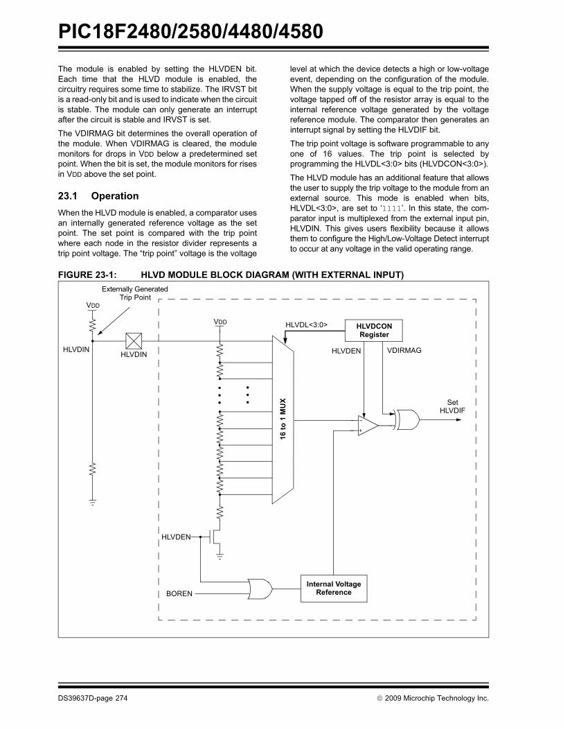
PIC18F2480/2580/4480/4580
The module is enabled by setting the HLVDEN bit.Each time that the HLVD module is enabled, thecircuitry requires some time to stabilize. The IRVST bitis a read-only bit and is used to indicate when the circuitis stable. The module can only generate an interruptafter the circuit is stable and IRVST is set.The VDIRMAG bit determines the overall operation ofthe module. When VDIRMAG is cleared, the modulemonitors for drops in VDD below a predetermined setpoint. When the bit is set, the module monitors for risesin VDD above the set point.
23.1 OperationWhen the HLVD module is enabled, a comparator usesan internally generated reference voltage as the setpoint. The set point is compared with the trip pointwhere each node in the resistor divider represents atrip point voltage. The “trip point” voltage is the voltage
level at which the device detects a high or low-voltageevent, depending on the configuration of the module.When the supply voltage is equal to the trip point, thevoltage tapped off of the resistor array is equal to theinternal reference voltage generated by the voltagereference module. The comparator then generates aninterrupt signal by setting the HLVDIF bit.
The trip point voltage is software programmable to anyone of 16 values. The trip point is selected byprogramming the HLVDL<3:0> bits (HLVDCON<3:0>).
The HLVD module has an additional feature that allowsthe user to supply the trip voltage to the module from anexternal source. This mode is enabled when bits,HLVDL<3:0>, are set to ‘1111’. In this state, the com-parator input is multiplexed from the external input pin,HLVDIN. This gives users flexibility because it allowsthem to configure the High/Low-Voltage Detect interruptto occur at any voltage in the valid operating range.
FIGURE 23-1: HLVD MODULE BLOCK DIAGRAM (WITH EXTERNAL INPUT)
Set
VDD
16 to
1 M
UX
HLVDEN
HLVDCON
HLVDIN
HLVDL<3:0>Register
HLVDIN
VDD
Externally GeneratedTrip Point
HLVDIF
HLVDEN
BORENInternal Voltage
Reference
VDIRMAG
DS39637D-page 274 © 2009 Microchip Technology Inc.

PIC18F2480/2580/4480/4580
23.2 HLVD SetupThe following steps are needed to set up the HLVDmodule:1. Disable the module by clearing the HLVDEN bit(HLVDCON<4>).
2. Write the value to the HLVDL<3:0> bits thatselect the desired HLVD trip point.
3. Set the VDIRMAG bit to detect high voltage(VDIRMAG = 1) or low voltage (VDIRMAG = 0).
4. Enable the HLVD module by setting theHLVDEN bit.
5. Clear the HLVD interrupt flag (PIR2<2>), whichmay have been set from a previous interrupt.
6. Enable the HLVD interrupt if interrupts aredesired by setting the HLVDIE and GIE bits(PIE<2> and INTCON<7>). An interrupt will notbe generated until the IRVST bit is set.
23.3 Current ConsumptionWhen the module is enabled, the HLVD comparatorand voltage divider are enabled and will consume staticcurrent. The total current consumption, when enabled,is specified in electrical specification parameter D022B.
Depending on the application, the HLVD module doesnot need to be operating constantly. To decrease thecurrent requirements, the HLVD circuitry may onlyneed to be enabled for short periods where the voltageis checked. After doing the check, the HLVD modulemay be disabled.
23.4 HLVD Start-up TimeThe internal reference voltage of the HLVD module,specified in electrical specification parameter D420,may be used by other internal circuitry, such as theProgrammable Brown-out Reset. If the HLVD or othercircuits using the voltage reference are disabled tolower the device’s current consumption, the referencevoltage circuit will require time to become stable beforea low or high-voltage condition can be reliablydetected. This start-up time, TIRVST, is an interval thatis independent of device clock speed. It is specified inelectrical specification parameter 36.
The HLVD interrupt flag is not enabled until TIRVST hasexpired and a stable reference voltage is reached. Forthis reason, brief excursions beyond the set point maynot be detected during this interval. Refer toFigure 23-2 or Figure 23-3.
FIGURE 23-2: LOW-VOLTAGE DETECT OPERATION (VDIRMAG = 0)
VLVD
VDD
HLVDIF
VLVD
VDD
Enable HLVD
TIRVST
HLVDIF may not be set
Enable HLVD
HLVDIF
HLVDIF cleared in software
HLVDIF cleared in software
HLVDIF cleared in software,
CASE 1:
CASE 2:
HLVDIF remains set since HLVD condition still exists
TIRVST
Internal Reference is stable
Internal Reference is stable
IRVST
IRVST
© 2009 Microchip Technology Inc. DS39637D-page 275

PIC18F2480/2580/4480/4580
FIGURE 23-3: HIGH-VOLTAGE DETECT OPERATION (VDIRMAG = 1)23.5 ApplicationsIn many applications, the ability to detect a drop below,or rise above a particular threshold is desirable. Forexample, the HLVD module could be periodicallyenabled to detect Universal Serial Bus (USB) attach ordetach. This assumes the device is powered by a lowervoltage source than the USB when detached. An attachwould indicate a high-voltage detect from, for example,3.3V to 5V (the voltage on USB) and vice versa for adetach. This feature could save a design a few extracomponents and an attach signal (input pin).
For general battery applications, Figure 23-4 shows apossible voltage curve. Over time, the device voltagedecreases. When the device voltage reaches voltage,VA, the HLVD logic generates an interrupt at time, TA.The interrupt could cause the execution of an ISR,which would allow the application to perform “house-keeping tasks” and perform a controlled shutdownbefore the device voltage exits the valid operatingrange at TB. The HLVD, thus, would give the applica-tion a time window, represented by the differencebetween TA and TB, to safely exit.
FIGURE 23-4: TYPICAL LOW-VOLTAGE DETECT APPLICATION
VLVD
VDD
HLVDIF
VLVDVDD
Enable HLVD
TIRVST
HLVDIF may not be set
Enable HLVD
HLVDIF
HLVDIF cleared in software
HLVDIF cleared in software
HLVDIF cleared in software,
CASE 1:
CASE 2:
HLVDIF remains set since HLVD condition still exists
TIRVST
IRVST
Internal Reference is stable
Internal Reference is stable
IRVST
Time
Volta
ge
VAVB
TA TB
VA = HLVD trip pointVB = Minimum valid device operating voltage
Legend:
DS39637D-page 276 © 2009 Microchip Technology Inc.

PIC18F2480/2580/4480/4580
23.6 Operation During SleepWhen enabled, the HLVD circuitry continues to operateduring Sleep. If the device voltage crosses the trippoint, the HLVDIF bit will be set and the device willwake-up from Sleep. Device execution will continuefrom the interrupt vector address if interrupts havebeen globally enabled.23.7 Effects of a Reset A device Reset forces all registers to their Reset state.This forces the HLVD module to be turned off.
TABLE 23-1: REGISTERS ASSOCIATED WITH HIGH/LOW-VOLTAGE DETECT MODULE
Name Bit 7 Bit 6 Bit 5 Bit 4 Bit 3 Bit 2 Bit 1 Bit 0Reset Values
on Page:
HLVDCON VDIRMAG — IRVST HLVDEN HLVDL3 HLVDL2 HLVDL1 HLVDL0 56INTCON GIE/GIEH PEIE/GIEL TMR0IE INT0IE RBIE TMR0IF INT0IF RBIF 55PIR2 OSCFIF CMIF — EEIF BCLIF HLVDIF TMR3IF ECCP1IF 58PIE2 OSCFIE CMIE — EEIE BCLIE HLVDIE TMR3IE ECCP1IE 58IPR2 OSCFIP CMIP — EEIP BCLIP HLVDIP TMR3IP ECCP1IP 57Legend: — = unimplemented, read as ‘0’. Shaded cells are unused by the HLVD module.
© 2009 Microchip Technology Inc. DS39637D-page 277

PIC18F2480/2580/4480/4580
NOTES:DS39637D-page 278 © 2009 Microchip Technology Inc.

PIC18F2480/2580/4480/4580
24.0 ECAN MODULEPIC18F2480/2580/4480/4580 devices contain anEnhanced Controller Area Network (ECAN) module.The ECAN module is fully backward compatible withthe CAN module available in PIC18CXX8 andPIC18FXX8 devices.
The Controller Area Network (CAN) module is a serialinterface which is useful for communicating with otherperipherals or microcontroller devices. This interface,or protocol, was designed to allow communicationswithin noisy environments.
The ECAN module is a communication controller, imple-menting the CAN 2.0A or B protocol as defined in theBOSCH specification. The module will support CAN 1.2,CAN 2.0A, CAN 2.0B Passive and CAN 2.0B Activeversions of the protocol. The module implementation isa full CAN system; however, the CAN specification is notcovered within this data sheet. Refer to the BOSCH CANspecification for further details.
The module features are as follows:
• Implementation of the CAN protocol, CAN 1.2, CAN 2.0A and CAN 2.0B
• DeviceNetTM data bytes filter support• Standard and extended data frames• 0-8 bytes data length• Programmable bit rate up to 1 Mbit/sec• Fully backward compatible with the PIC18XXX8
CAN module• Three modes of operation:
- Mode 0 – Legacy mode- Mode 1 – Enhanced Legacy mode with
DeviceNet support- Mode 2 – FIFO mode with DeviceNet support
• Support for remote frames with automated handling• Double-buffered receiver with two prioritized
received message storage buffers• Six buffers programmable as RX and TX
message buffers• 16 full (standard/extended identifier) acceptance
filters that can be linked to one of four masks• Two full acceptance filter masks that can be
assigned to any filter• One full acceptance filter that can be used as either
an acceptance filter or acceptance filter mask• Three dedicated transmit buffers with application
specified prioritization and abort capability• Programmable wake-up functionality with
integrated low-pass filter• Programmable Loopback mode supports self-test
operation• Signaling via interrupt capabilities for all CAN
receiver and transmitter error states• Programmable clock source• Programmable link to timer module for
time-stamping and network synchronization• Low-power Sleep mode
24.1 Module OverviewThe CAN bus module consists of a protocol engine andmessage buffering and control. The CAN protocolengine automatically handles all functions for receivingand transmitting messages on the CAN bus. Messagesare transmitted by first loading the appropriate dataregisters. Status and errors can be checked by readingthe appropriate registers. Any message detected onthe CAN bus is checked for errors and then matchedagainst filters to see if it should be received and storedin one of the two receive registers.
The CAN module supports the following frame types:
• Standard Data Frame• Extended Data Frame• Remote Frame• Error Frame• Overload Frame Reception
The CAN module uses the RB2/CANTX and RB3/CANRX pins to interface with the CAN bus. In normalmode, the CAN module automatically overridesTRISB<2>. The user must ensure that TRISB<3> isset.
24.1.1 MODULE FUNCTIONALITYThe CAN bus module consists of a protocol engine,message buffering and control (see Figure 24-1). Theprotocol engine can best be understood by defining thetypes of data frames to be transmitted and received bythe module.
The following sequence illustrates the necessary initial-ization steps before the ECAN module can be used totransmit or receive a message. Steps can be added orremoved depending on the requirements of theapplication.
1. Initial LAT and TRIS bits for RX and TX CAN.2. Ensure that the ECAN module is in Configuration
mode.3. Select ECAN Operational mode.4. Set up the Baud Rate registers.5. Set up the Filter and Mask registers.6. Set the ECAN module to normal mode or any
other mode required by the application logic.
© 2009 Microchip Technology Inc. DS39637D-page 279

PIC18F2480/2580/4480/4580
FIGURE 24-1: CAN BUFFERS AND PROTOCOL ENGINE BLOCK DIAGRAMMS
GR
EQ
TXB2
ABTF
MLO
ATX
ERR
MTX
BU
FF
ME
SSA
GE
MessageQueueControl
Transmit Byte Sequencer
MS
GR
EQ
TXB1
ABTF
MLO
ATX
ERR
MTX
BU
FF
ME
SSA
GE
MS
GR
EQ
TXB0
ABTF
MLO
ATX
ERR
MTX
BU
FF
ME
SSA
GE
Acceptance Filters(RXF0-RXF05)
Accept
Data Field
Identifier
Acc
epta
nce
Mas
kR
XM
1Acceptance Filters(RXF06-RXF15)
MAB
Acc
epta
nce
Mas
kR
XM
0
Rcv Byte
16 - 4 to 1 MUXs
PROTOCOL
MESSAGEBUFFERS
Transmit Option
MODE 0
MODE 1, 26 TX/RXBuffers
2 RXBuffers
CRC<14:0>
Comparator
Receive<8:0>Transmit<7:0>
ReceiveError
TransmitError
Protocol
REC
TEC
Err-PasBus-Off
FiniteState
Machine
Counter
Counter
Shift<14:0>Transmit<5:0>, Receive<8:0>
TransmitLogic
BitTimingLogic
TX RX ConfigurationRegisters
ClockGenerator
BUFFERS
ENGINE
MODE 0
MODE 1, 2
RXF15
VCC
DS39637D-page 280 © 2009 Microchip Technology Inc.

PIC18F2480/2580/4480/4580
24.2 CAN Module RegistersThere are many control and data registers associatedwith the CAN module. For convenience, theirdescriptions have been grouped into the followingsections:
• Control and Status Registers• Dedicated Transmit Buffer Registers• Dedicated Receive Buffer Registers• Programmable TX/RX and Auto RTR Buffers• Baud Rate Control Registers• I/O Control Register• Interrupt Status and Control Registers
Detailed descriptions of each register and their usageare described in the following sections.
24.2.1 CAN CONTROL AND STATUS REGISTERS
The registers described in this section control theoverall operation of the CAN module and show itsoperational status.
Note: Not all CAN registers are available in theAccess Bank.
© 2009 Microchip Technology Inc. DS39637D-page 281

PIC18F2480/2580/4480/4580
REGISTER 24-1: CANCON: CAN CONTROL REGISTERMode 0R/W-1 R/W-0 R/W-0 R/S-0 R/W-0 R/W-0 R/W-0 U-0
REQOP2 REQOP1 REQOP0 ABAT WIN2 WIN1 WIN0 —
Mode 1R/W-1 R/W-0 R/W-0 R/S-0 U0 U-0 U-0 U-0
REQOP2 REQOP1 REQOP0 ABAT — — — —
Mode 2R/W-1 R/W-0 R/W-0 R/S-0 R-0 R-0 R-0 R-0
REQOP2 REQOP1 REQOP0 ABAT FP3 FP2 FP1 FP0bit 7 bit 0
Legend: S = Settable bitR = Readable bit W = Writable bit U = Unimplemented bit, read as ‘0’-n = Value at POR ‘1’ = Bit is set ‘0’ = Bit is cleared x = Bit is unknown
bit 7-5 REQOP<2:0>: Request CAN Operation Mode bits1xx = Request Configuration mode 011 = Request Listen Only mode 010 = Request Loopback mode 001 = Disabled/Sleep mode000 = Request Normal mode
bit 4 ABAT: Abort All Pending Transmissions bit1 = Abort all pending transmissions (in all transmit buffers)(1) 0 = Transmissions proceeding as normal
bit 3-1 Mode 0:WIN<2:0>: Window Address bitsThese bits select which of the CAN buffers to switch into the Access Bank area. This allows access to the buffer registers from any data memory bank. After a frame has caused an interrupt, the ICODE<3:0> bits can be copied to the WIN<2:0> bits to select the correct buffer. See Example 24-2 for a code example.111 = Receive Buffer 0 110 = Receive Buffer 0 101 = Receive Buffer 1 100 = Transmit Buffer 0 011 = Transmit Buffer 1 010 = Transmit Buffer 2 001 = Receive Buffer 0 000 = Receive Buffer 0
bit 0 Unimplemented: Read as ‘0’bit 4-0 Mode 1:
Unimplemented: Read as ‘0’Mode 2:FP<3:0>: FIFO Read Pointer bitsThese bits point to the message buffer to be read.0000 = Receive Message Buffer 00001 = Receive Message Buffer 10010 = Receive Message Buffer 20011 = Receive Message Buffer 30100 = Receive Message Buffer 40101 = Receive Message Buffer 50110 = Receive Message Buffer 60111 = Receive Message Buffer 71000:1111 Reserved
Note 1: This bit will clear when all transmissions are aborted.
DS39637D-page 282 © 2009 Microchip Technology Inc.

PIC18F2480/2580/4480/4580
REGISTER 24-2: CANSTAT: CAN STATUS REGISTERMode 0R-1 R-0 R-0 R-0 R-0 R-0 R-0 U-0
OPMODE2(1) OPMODE1(1) OPMODE0(1) — ICODE3 ICODE2 ICODE1 —
Mode 1,2R-1 R-0 R-0 R-0 R-0 R-0 R-0 R-0
OPMODE2(1) OPMODE1(1) OPMODE0(1) EICODE4 EICODE3 EICODE2 EICODE1 EICODE0bit 7 bit 0
Legend:R = Readable bit W = Writable bit U = Unimplemented bit, read as ‘0’-n = Value at POR ‘1’ = Bit is set ‘0’ = Bit is cleared x = Bit is unknown
bit 7-5 OPMODE<2:0>: Operation Mode Status bits(1)
111 = Reserved 110 = Reserved 101 = Reserved 100 = Configuration mode 011 = Listen Only mode 010 = Loopback mode 001 = Disable/Sleep mode 000 = Normal mode
bit 4 Mode 0:Unimplemented: Read as ‘0’
bit 3-1 ICODE<3:1>: Interrupt Code bitsWhen an interrupt occurs, a prioritized coded interrupt value will be present in these bits. This codeindicates the source of the interrupt. By copying ICODE<3:1> to WIN<3:0> (Mode 0) or EICODE<4:0> toEWIN<4:0> (Mode 1 and 2), it is possible to select the correct buffer to map into the Access Bank area.See Example 24-2 for a code example. To simplify the description, the following table lists all five bits.
bit 0 Unimplemented: Read as ‘0’bit 4-0 Mode 1, 2:
EICODE<4:0>: Interrupt Code bitsSee ICODE<3:1> above.
Note 1: To achieve maximum power saving and/or able to wake-up on CAN bus activity, switch CAN module in Disable/Sleep mode before putting device to Sleep.
2: If buffer is configured as receiver, EICODE bits will contain ‘10000’ upon interrupt.
Mode 0 Mode 1 Mode 2No interrupt 00000 00000 00000CAN bus error interrupt 00010 00010 00010TXB2 interrupt 00100 00100 00100TXB1 interrupt 00110 00110 00110TXB0 interrupt 01000 01000 01000RXB1 interrupt 01010 10001 -----RXB0 interrupt 01100 10000 10000Wake-up interrupt 00010 01110 01110RXB0 interrupt ----- 10000 10000RXB1 interrupt ----- 10001 10000RX/TX B0 interrupt ----- 10010 10010(2)
RX/TX B1 interrupt ----- 10011 10011(2)
RX/TX B2 interrupt ----- 10100 10100(2)
RX/TX B3 interrupt ----- 10101 10101(2)
RX/TX B4 interrupt ----- 10110 10110(2)
RX/TX B5 interrupt ----- 10111 10111(2)
© 2009 Microchip Technology Inc. DS39637D-page 283

PIC18F2480/2580/4480/4580
EXAMPLE 24-1: CHANGING TO CONFIGURATION MODEEXAMPLE 24-2: WIN AND ICODE BITS USAGE IN INTERRUPT SERVICE ROUTINE TO ACCESS TX/RX BUFFERS
; Request Configuration mode.MOVLW B’10000000’ ; Set to Configuration Mode.MOVWF CANCON; A request to switch to Configuration mode may not be immediately honored. ; Module will wait for CAN bus to be idle before switching to Configuration Mode.; Request for other modes such as Loopback, Disable etc. may be honored immediately. ; It is always good practice to wait and verify before continuing.
ConfigWait:MOVF CANSTAT, W ; Read current mode state.ANDLW B’10000000’ ; Interested in OPMODE bits only.TSTFSZ WREG ; Is it Configuration mode yet?BRA ConfigWait ; No. Continue to wait...; Module is in Configuration mode now.; Modify configuration registers as required.; Switch back to Normal mode to be able to communicate.
; Save application required context.; Poll interrupt flags and determine source of interrupt; This was found to be CAN interrupt; TempCANCON and TempCANSTAT are variables defined in Access Bank lowMOVFF CANCON, TempCANCON ; Save CANCON.WIN bits
; This is required to prevent CANCON; from corrupting CAN buffer access; in-progress while this interrupt; occurred
MOVFF CANSTAT, TempCANSTAT ; Save CANSTAT register; This is required to make sure that; we use same CANSTAT value rather; than one changed by another CAN; interrupt.
MOVF TempCANSTAT, W ; Retrieve ICODE bitsANDLW B’00001110’ADDWF PCL, F ; Perform computed GOTO
; to corresponding interrupt causeBRA NoInterrupt ; 000 = No interruptBRA ErrorInterrupt ; 001 = Error interruptBRA TXB2Interrupt ; 010 = TXB2 interruptBRA TXB1Interrupt ; 011 = TXB1 interruptBRA TXB0Interrupt ; 100 = TXB0 interruptBRA RXB1Interrupt ; 101 = RXB1 interruptBRA RXB0Interrupt ; 110 = RXB0 interrupt
; 111 = Wake-up on interruptWakeupInterrupt
BCF PIR3, WAKIF ; Clear the interrupt flag;; User code to handle wake-up procedure;;; Continue checking for other interrupt source or return from here…
NoInterrupt… ; PC should never vector here. User may
; place a trap such as infinite loop or pin/port; indication to catch this error.
DS39637D-page 284 © 2009 Microchip Technology Inc.

PIC18F2480/2580/4480/4580
EXAMPLE 24-2: WIN AND ICODE BITS USAGE IN INTERRUPT SERVICE ROUTINE TO ACCESSTX/RX BUFFERS (CONTINUED)ErrorInterrupt
BCF PIR3, ERRIF ; Clear the interrupt flag… ; Handle error.RETFIE
TXB2InterruptBCF PIR3, TXB2IF ; Clear the interrupt flagGOTO AccessBuffer
TXB1InterruptBCF PIR3, TXB1IF ; Clear the interrupt flagGOTO AccessBuffer
TXB0InterruptBCF PIR3, TXB0IF ; Clear the interrupt flagGOTO AccessBuffer
RXB1InterruptBCF PIR3, RXB1IF ; Clear the interrupt flagGOTO Accessbuffer
RXB0InterruptBCF PIR3, RXB0IF ; Clear the interrupt flagGOTO AccessBuffer
AccessBuffer ; This is either TX or RX interrupt; Copy CANSTAT.ICODE bits to CANCON.WIN bitsMOVF TempCANCON, W ; Clear CANCON.WIN bits before copying
; new ones.ANDLW B’11110001’ ; Use previously saved CANCON value to
; make sure same value.MOVWF TempCANCON ; Copy masked value back to TempCANCONMOVF TempCANSTAT, W ; Retrieve ICODE bitsANDLW B’00001110’ ; Use previously saved CANSTAT value
; to make sure same value.IORWF TempCANCON ; Copy ICODE bits to WIN bits.MOVFF TempCANCON, CANCON ; Copy the result to actual CANCON; Access current buffer…; User code; Restore CANCON.WIN bitsMOVF CANCON, W ; Preserve current non WIN bitsANDLW B’11110001’IORWF TempCANCON ; Restore original WIN bits; Do not need to restore CANSTAT - it is read-only register.; Return from interrupt or check for another module interrupt source
© 2009 Microchip Technology Inc. DS39637D-page 285

PIC18F2480/2580/4480/4580
REGISTER 24-3: ECANCON: ENHANCED CAN CONTROL REGISTERR/W-0 R/W-0 R/W-0 R/W-1 R/W-0 R/W-0 R/W-0 R/W-0MDSEL1(1) MDSEL0(1) FIFOWM(2) EWIN4 EWIN3 EWIN2 EWIN1 EWIN0
bit 7 bit 0
Legend:R = Readable bit W = Writable bit U = Unimplemented bit, read as ‘0’-n = Value at POR ‘1’ = Bit is set ‘0’ = Bit is cleared x = Bit is unknown
bit 7-6 MDSEL<1:0>: Mode Select bits(1)
00 = Legacy mode (Mode 0, default)01 = Enhanced Legacy mode (Mode 1)10 = Enhanced FIFO mode (Mode 2)11 = Reserved
bit 5 FIFOWM: FIFO High Water Mark bit(2)
1 = Will cause FIFO interrupt when one receive buffer remains0 = Will cause FIFO interrupt when four receive buffers remain(3)
bit 4-0 EWIN<4:0>: Enhanced Window Address bitsThese bits map the group of 16 banked CAN SFRs into Access Bank addresses 0F60-0F6Dh. Theexact group of registers to map is determined by the binary value of these bits.Mode 0:Unimplemented: Read as ‘0’Mode 1, 2:00000 = Acceptance Filters 0, 1, 2 and BRGCON2, 300001 = Acceptance Filters 3, 4, 5 and BRGCON1, CIOCON00010 = Acceptance Filter Masks, Error and Interrupt Control00011 = Transmit Buffer 000100 = Transmit Buffer 100101 = Transmit Buffer 200110 = Acceptance Filters 6, 7, 800111 = Acceptance Filters 9, 10, 1101000 = Acceptance Filters 12, 13, 1401001 = Acceptance Filters 1501010-01110 = Reserved01111 = RXINT0, RXINT110000 = Receive Buffer 010001 = Receive Buffer 110010 = TX/RX Buffer 010011 = TX/RX Buffer 110100 = TX/RX Buffer 210101 = TX/RX Buffer 310110 = TX/RX Buffer 410111 = TX/RX Buffer 511000-11111 = Reserved
Note 1: These bits can only be changed in Configuration mode. See Register 24-1 to change to Configuration mode.2: This bit is used in Mode 2 only.3: If FIFO is configured to contain four or less buffers, then the FIFO interrupt will trigger.
DS39637D-page 286 © 2009 Microchip Technology Inc.

PIC18F2480/2580/4480/4580
REGISTER 24-4: COMSTAT: COMMUNICATION STATUS REGISTERMode 0R/C-0 R/C-0 R-0 R-0 R-0 R-0 R-0 R-0
RXB0OVFL RXB1OVFL TXBO TXBP RXBP TXWARN RXWARN EWARN
Mode 1R/C-0 R/C-0 R-0 R-0 R-0 R-0 R-0 R-0
— RXBnOVFL TXB0 TXBP RXBP TXWARN RXWARN EWARN
Mode 2R/C-0 R/C-0 R-0 R-0 R-0 R-0 R-0 R-0
FIFOEMPTY RXBnOVFL TXBO TXBP RXBP TXWARN RXWARN EWARNbit 7 bit 0
Legend: C = Clearable bitR = Readable bit W = Writable bit U = Unimplemented bit, read as ‘0’-n = Value at POR ‘1’ = Bit is set ‘0’ = Bit is cleared x = Bit is unknown
bit 7 Mode 0:RXB0OVFL: Receive Buffer 0 Overflow bit1 = Receive Buffer 0 overflowed 0 = Receive Buffer 0 has not overflowedMode 1:Unimplemented: Read as ‘0’Mode 2:FIFOEMPTY: FIFO Not Empty bit1 = Receive FIFO is not empty0 = Receive FIFO is empty
bit 6 Mode 0:RXB1OVFL: Receive Buffer 1 Overflow bit1 = Receive Buffer 1 overflowed 0 = Receive Buffer 1 has not overflowed Mode 1, 2:RXBnOVFL: Receive Buffer n Overflow bit1 = Receive Buffer n has overflowed 0 = Receive Buffer n has not overflowed
bit 5 TXBO: Transmitter Bus-Off bit1 = Transmit error counter > 255 0 = Transmit error counter ≤ 255
bit 4 TXBP: Transmitter Bus Passive bit1 = Transmit error counter > 127 0 = Transmit error counter ≤ 127
bit 3 RXBP: Receiver Bus Passive bit1 = Receive error counter > 127 0 = Receive error counter ≤ 127
bit 2 TXWARN: Transmitter Warning bit1 = Transmit error counter > 95 0 = Transmit error counter ≤ 95
bit 1 RXWARN: Receiver Warning bit1 = 127 ≥ Receive error counter > 95 0 = Receive error counter ≤ 95
bit 0 EWARN: Error Warning bitThis bit is a flag of the RXWARN and TXWARN bits.1 = The RXWARN or the TXWARN bits are set 0 = Neither the RXWARN or the TXWARN bits are set
© 2009 Microchip Technology Inc. DS39637D-page 287

PIC18F2480/2580/4480/4580
24.2.2 DEDICATED CAN TRANSMITBUFFER REGISTERSThis section describes the dedicated CAN TransmitBuffer registers and their associated control registers.
REGISTER 24-5: TXBnCON: TRANSMIT BUFFER n CONTROL REGISTERS [0 ≤ n ≤ 2]
Mode 0U-0 R-0 R-0 R-0 R/W-0 U-0 R/W-0 R/W-0— TXABT(1) TXLARB(1) TXERR(1) TXREQ(2) — TXPRI1(3) TXPRI0(3)
Mode 1,2R/C-0 R-0 R-0 R-0 R/W-0 U-0 R/W-0 R/W-0TXBIF TXABT(1) TXLARB(1) TXERR(1) TXREQ(2) — TXPRI1(3) TXPRI0(3)
bit 7 bit 0
Legend: C = Clearable bitR = Readable bit W = Writable bit U = Unimplemented bit, read as ‘0’-n = Value at POR ‘1’ = Bit is set ‘0’ = Bit is cleared x = Bit is unknown
bit 7 Mode 0:Unimplemented: Read as ‘0’Mode 1, 2:TXBIF: Transmit Buffer Interrupt Flag bit1 = Transmit buffer has completed transmission of message and may be reloaded0 = Transmit buffer has not completed transmission of a message
bit 6 TXABT: Transmission Aborted Status bit(1)
1 = Message was aborted 0 = Message was not aborted
bit 5 TXLARB: Transmission Lost Arbitration Status bit(1)
1 = Message lost arbitration while being sent 0 = Message did not lose arbitration while being sent
bit 4 TXERR: Transmission Error Detected Status bit(1) 1 = A bus error occurred while the message was being sent 0 = A bus error did not occur while the message was being sent
bit 3 TXREQ: Transmit Request Status bit(2)
1 = Requests sending a message. Clears the TXABT, TXLARB and TXERR bits.0 = Automatically cleared when the message is successfully sent
bit 2 Unimplemented: Read as ‘0’ bit 1-0 TXPRI<1:0>: Transmit Priority bits(3)
11 = Priority Level 3 (highest priority) 10 = Priority Level 2 01 = Priority Level 100 = Priority Level 0 (lowest priority)
Note 1: This bit is automatically cleared when TXREQ is set.2: While TXREQ is set, Transmit Buffer registers remain read-only. Clearing this bit in software while the bit is
set will request a message abort.3: These bits define the order in which transmit buffers will be transferred. They do not alter the CAN
message identifier.
DS39637D-page 288 © 2009 Microchip Technology Inc.

PIC18F2480/2580/4480/4580
REGISTER 24-6: TXBnSIDH: TRANSMIT BUFFER n STANDARD IDENTIFIER REGISTERS, HIGH BYTE [0 ≤ n ≤ 2]
R/W-x R/W-x R/W-x R/W-x R/W-x R/W-x R/W-x R/W-xSID10 SID9 SID8 SID7 SID6 SID5 SID4 SID3
bit 7 bit 0
Legend:R = Readable bit W = Writable bit U = Unimplemented bit, read as ‘0’-n = Value at POR ‘1’ = Bit is set ‘0’ = Bit is cleared x = Bit is unknown
bit 7-0 SID<10:3>: Standard Identifier bits (if EXIDE (TXBnSIDL<3>) = 0)Extended Identifier bits EID<28:21> (if EXIDE = 1).
REGISTER 24-7: TXBnSIDL: TRANSMIT BUFFER n STANDARD IDENTIFIER REGISTERS, LOW BYTE [0 ≤ n ≤ 2]
R/W-x R/W-x R/W-x U-0 R/W-x U-0 R/W-x R/W-xSID2 SID1 SID0 — EXIDE — EID17 EID16
bit 7 bit 0
Legend:R = Readable bit W = Writable bit U = Unimplemented bit, read as ‘0’-n = Value at POR ‘1’ = Bit is set ‘0’ = Bit is cleared x = Bit is unknown
bit 7-5 SID<2:0>: Standard Identifier bits (if EXIDE (TXBnSIDL<3>) = 0)Extended Identifier bits EID<20:18> (if EXIDE = 1).
bit 4 Unimplemented: Read as ‘0’bit 3 EXIDE: Extended Identifier Enable bit
1 = Message will transmit extended ID, SID<10:0> become EID<28:18>0 = Message will transmit standard ID, EID<17:0> are ignored
bit 2 Unimplemented: Read as ‘0’bit 1-0 EID<17:16>: Extended Identifier bits
REGISTER 24-8: TXBnEIDH: TRANSMIT BUFFER n EXTENDED IDENTIFIER REGISTERS, HIGH BYTE [0 ≤ n ≤ 2]
R/W-x R/W-x R/W-x R/W-x R/W-x R/W-x R/W-x R/W-xEID15 EID14 EID13 EID12 EID11 EID10 EID9 EID8
bit 7 bit 0
Legend:R = Readable bit W = Writable bit U = Unimplemented bit, read as ‘0’-n = Value at POR ‘1’ = Bit is set ‘0’ = Bit is cleared x = Bit is unknown
bit 7-0 EID<15:8>: Extended Identifier bits (not used when transmitting standard identifier message)
© 2009 Microchip Technology Inc. DS39637D-page 289

PIC18F2480/2580/4480/4580
REGISTER 24-9: TXBnEIDL: TRANSMIT BUFFER n EXTENDED IDENTIFIER REGISTERS, LOW BYTE [0 ≤ n ≤ 2]
R/W-x R/W-x R/W-x R/W-x R/W-x R/W-x R/W-x R/W-xEID7 EID6 EID5 EID4 EID3 EID2 EID1 EID0
bit 7 bit 0
Legend:R = Readable bit W = Writable bit U = Unimplemented bit, read as ‘0’-n = Value at POR ‘1’ = Bit is set ‘0’ = Bit is cleared x = Bit is unknown
bit 7-0 EID<7:0>: Extended Identifier bits (not used when transmitting standard identifier message)
REGISTER 24-10: TXBnDm: TRANSMIT BUFFER n DATA FIELD BYTE m REGISTERS [0 ≤ n ≤ 2, 0 ≤ m ≤ 7]
R/W-x R/W-x R/W-x R/W-x R/W-x R/W-x R/W-x R/W-xTXBnDm7 TXBnDm6 TXBnDm5 TXBnDm4 TXBnDm3 TXBnDm2 TXBnDm1 TXBnDm0
bit 7 bit 0
Legend:R = Readable bit W = Writable bit U = Unimplemented bit, read as ‘0’-n = Value at POR ‘1’ = Bit is set ‘0’ = Bit is cleared x = Bit is unknown
bit 7-0 TXBnDm<7:0>: Transmit Buffer n Data Field Byte m bits (where 0 ≤ n < 3 and 0 ≤ m < 8)Each transmit buffer has an array of registers. For example, Transmit Buffer 0 has 7 registers: TXB0D0to TXB0D7.
DS39637D-page 290 © 2009 Microchip Technology Inc.

PIC18F2480/2580/4480/4580
REGISTER 24-11: TXBnDLC: TRANSMIT BUFFER n DATA LENGTH CODE REGISTERS [0 ≤ n ≤ 2]
U-0 R/W-x U-0 U-0 R/W-x R/W-x R/W-x R/W-x— TXRTR — — DLC3 DLC2 DLC1 DLC0
bit 7 bit 0
Legend:R = Readable bit W = Writable bit U = Unimplemented bit, read as ‘0’-n = Value at POR ‘1’ = Bit is set ‘0’ = Bit is cleared x = Bit is unknown
bit 7 Unimplemented: Read as ‘0’bit 6 TXRTR: Transmit Remote Frame Transmission Request bit
1 = Transmitted message will have TXRTR bit set 0 = Transmitted message will have TXRTR bit cleared
bit 5-4 Unimplemented: Read as ‘0’bit 3-0 DLC<3:0>: Data Length Code bits
1111 = Reserved 1110 = Reserved 1101 = Reserved 1100 = Reserved 1011 = Reserved 1010 = Reserved 1001 = Reserved 1000 = Data length = 8 bytes 0111 = Data length = 7 bytes 0110 = Data length = 6 bytes 0101 = Data length = 5 bytes 0100 = Data length = 4 bytes 0011 = Data length = 3 bytes 0010 = Data length = 2 bytes 0001 = Data length = 1 bytes 0000 = Data length = 0 bytes
REGISTER 24-12: TXERRCNT: TRANSMIT ERROR COUNT REGISTER
R-0 R-0 R-0 R-0 R-0 R-0 R-0 R-0TEC7 TEC6 TEC5 TEC4 TEC3 TEC2 TEC1 TEC0
bit 7 bit 0
Legend:R = Readable bit W = Writable bit U = Unimplemented bit, read as ‘0’-n = Value at POR ‘1’ = Bit is set ‘0’ = Bit is cleared x = Bit is unknown
bit 7-0 TEC<7:0>: Transmit Error Counter bitsThis register contains a value which is derived from the rate at which errors occur. When the errorcount overflows, the bus-off state occurs. When the bus has 128 occurrences of 11 consecutiverecessive bits, the counter value is cleared.
© 2009 Microchip Technology Inc. DS39637D-page 291

PIC18F2480/2580/4480/4580
EXAMPLE 24-3: TRANSMITTING A CAN MESSAGE USING BANKED METHODEXAMPLE 24-4: TRANSMITTING A CAN MESSAGE USING WIN BITS
; Need to transmit Standard Identifier message 123h using TXB0 buffer.; To successfully transmit, CAN module must be either in Normal or Loopback mode.; TXB0 buffer is not in access bank. And since we want banked method, we need to make sure; that correct bank is selected.BANKSEL TXB0CON ; One BANKSEL in beginning will make sure that we are
; in correct bank for rest of the buffer access.; Now load transmit data into TXB0 buffer.MOVLW MY_DATA_BYTE1 ; Load first data byte into bufferMOVWF TXB0D0 ; Compiler will automatically set “BANKED” bit; Load rest of data bytes - up to 8 bytes into TXB0 buffer....; Load message identifierMOVLW 60H ; Load SID2:SID0, EXIDE = 0MOVWF TXB0SIDLMOVLW 24H ; Load SID10:SID3MOVWF TXB0SIDH; No need to load TXB0EIDL:TXB0EIDH, as we are transmitting Standard Identifier Message only.
; Now that all data bytes are loaded, mark it for transmission.MOVLW B’00001000’ ; Normal priority; Request transmissionMOVWF TXB0CON
; If required, wait for message to get transmittedBTFSC TXB0CON, TXREQ ; Is it transmitted?BRA $-2 ; No. Continue to wait...
; Message is transmitted.
; Need to transmit Standard Identifier message 123h using TXB0 buffer.; To successfully transmit, CAN module must be either in Normal or Loopback mode.; TXB0 buffer is not in access bank. Use WIN bits to map it to RXB0 area.MOVF CANCON, W ; WIN bits are in lower 4 bits only. Read CANCON
; register to preserve all other bits. If operation; mode is already known, there is no need to preserve; other bits.
ANDLW B’11110000’ ; Clear WIN bits.IORLW B’00001000’ ; Select Transmit Buffer 0MOVWF CANCON ; Apply the changes.; Now TXB0 is mapped in place of RXB0. All future access to RXB0 registers will actually; yield TXB0 register values.
; Load transmit data into TXB0 buffer.MOVLW MY_DATA_BYTE1 ; Load first data byte into bufferMOVWF RXB0D0 ; Access TXB0D0 via RXB0D0 address.; Load rest of the data bytes - up to 8 bytes into “TXB0” buffer using RXB0 registers....; Load message identifierMOVLW 60H ; Load SID2:SID0, EXIDE = 0MOVWF RXB0SIDLMOVLW 24H ; Load SID10:SID3MOVWF RXB0SIDH; No need to load RXB0EIDL:RXB0EIDH, as we are transmitting Standard Identifier Message only.
; Now that all data bytes are loaded, mark it for transmission.MOVLW B’00001000’ ; Normal priority; Request transmissionMOVWF RXB0CON
; If required, wait for message to get transmittedBTFSC RXB0CON, TXREQ ; Is it transmitted?BRA $-2 ; No. Continue to wait...
; Message is transmitted.; If required, reset the WIN bits to default state.
DS39637D-page 292 © 2009 Microchip Technology Inc.

PIC18F2480/2580/4480/4580
24.2.3 DEDICATED CAN RECEIVEBUFFER REGISTERSThis section shows the dedicated CAN Receive Bufferregisters with their associated control registers.
REGISTER 24-13: RXB0CON: RECEIVE BUFFER 0 CONTROL REGISTER
Mode 0R/C-0 R/W-0 R/W-0 U-0 R-0 R/W-0 R-0 R-0
RXFUL(1) RXM1 RXM0 — RXRTRRO RXB0DBEN JTOFF(2) FILHIT0
Mode 1,2R/C-0 R/W-0 R-0 R-0 R-0 R-0 R-0 R-0
RXFUL(1) RXM1 RTRRO FILHIT4 FILHIT3 FILHIT2 FILHIT1 FILHIT0bit 7 bit 0
Legend: C = Clearable bitR = Readable bit W = Writable bit U = Unimplemented bit, read as ‘0’-n = Value at POR ‘1’ = Bit is set ‘0’ = Bit is cleared x = Bit is unknown
bit 7 RXFUL: Receive Full Status bit(1)
1 = Receive buffer contains a received message0 = Receive buffer is open to receive a new message
bit 6 Mode 0:RXM1: Receive Buffer Mode bit 1 (combines with RXM0 to form RXM<1:0> bits, see bit 5)11 = Receive all messages (including those with errors); filter criteria is ignored 10 = Receive only valid messages with extended identifier; EXIDEN in RXFnSIDL must be ‘1’01 = Receive only valid messages with standard identifier; EXIDEN in RXFnSIDL must be ‘0’00 = Receive all valid messages as per EXIDEN bit in the RXFnSIDL registerMode 1, 2:RXM1: Receive Buffer Mode bit 11 = Receive all messages (including those with errors); acceptance filters are ignored 0 = Receive all valid messages as per acceptance filters
bit 5 Mode 0:RXM0: Receive Buffer Mode bit 0 (combines with RXM1 to form RXM<1:0>bits, see bit 6)Mode 1, 2:RTRRO: Remote Transmission Request bit for Received Message (read-only)1 = A remote transmission request is received0 = A remote transmission request is not received
bit 4 Mode 0:Unimplemented: Read as ‘0’ Mode 1, 2:FILHIT4: Filter Hit bit 4This bit combines with other bits to form filter acceptance bits<4:0>.
bit 3 Mode 0:RXRTRRO: Remote Transmission Request bit for Received Message (read-only)1 = A remote transmission request is received0 = A remote transmission request is not receivedMode 1, 2:FILHIT3: Filter Hit bit 3This bit combines with other bits to form filter acceptance bits<4:0>.
Note 1: This bit is set by the CAN module upon receiving a message and must be cleared by software after the buffer is read. As long as RXFUL is set, no new message will be loaded and buffer will be considered full. After clearing the RXFUL flag, the PIR3 bit, RXB0IF, can be cleared. If RXB0IF is cleared, but RXFUL is not cleared, then RXB0IF is set again.
2: This bit allows same filter jump table for both RXB0CON and RXB1CON.
© 2009 Microchip Technology Inc. DS39637D-page 293

PIC18F2480/2580/4480/4580
bit 2 Mode 0:RXB0DBEN: Receive Buffer 0 Double-Buffer Enable bit 1 = Receive Buffer 0 overflow will write to Receive Buffer 1 0 = No Receive Buffer 0 overflow to Receive Buffer 1 Mode 1, 2:FILHIT2: Filter Hit bit 2This bit combines with other bits to form filter acceptance bits<4:0>.
bit 1 Mode 0:JTOFF: Jump Table Offset bit (read-only copy of RXB0DBEN)(2)
1 = Allows jump table offset between 6 and 7 0 = Allows jump table offset between 1 and 0Mode 1, 2:FILHIT1: Filter Hit bit 1This bit combines with other bits to form filter acceptance bits<4:0>.
bit 0 Mode 0:FILHIT0: Filter Hit bit 0This bit indicates which acceptance filter enabled the message reception into Receive Buffer 0.1 = Acceptance Filter 1 (RXF1) 0 = Acceptance Filter 0 (RXF0)Mode 1, 2:FILHIT0: Filter Hit bit 0This bit, in combination with FILHIT<4:1>, indicates which acceptance filter enabled the message reception into this receive buffer.01111 = Acceptance Filter 15 (RXF15) 01110 = Acceptance Filter 14 (RXF14)...00000 = Acceptance Filter 0 (RXF0)
REGISTER 24-13: RXB0CON: RECEIVE BUFFER 0 CONTROL REGISTER (CONTINUED)
Note 1: This bit is set by the CAN module upon receiving a message and must be cleared by software after the buffer is read. As long as RXFUL is set, no new message will be loaded and buffer will be considered full. After clearing the RXFUL flag, the PIR3 bit, RXB0IF, can be cleared. If RXB0IF is cleared, but RXFUL is not cleared, then RXB0IF is set again.
2: This bit allows same filter jump table for both RXB0CON and RXB1CON.
DS39637D-page 294 © 2009 Microchip Technology Inc.

PIC18F2480/2580/4480/4580
REGISTER 24-14: RXB1CON: RECEIVE BUFFER 1 CONTROL REGISTERMode 0R/C-0 R/W-0 R/W-0 U-0 R-0 R/W-0 R-0 R-0
RXFUL(1) RXM1 RXM0 — RXRTRRO FILHIT2 FILHIT1 FILHIT0
Mode 1,2R/C-0 R/W-0 R-0 R-0 R-0 R-0 R-0 R-0
RXFUL(1) RXM1 RTRRO FILHIT4 FILHIT3 FILHIT2 FILHIT1 FILHIT0bit 7 bit 0
Legend: C = Clearable bitR = Readable bit W = Writable bit U = Unimplemented bit, read as ‘0’-n = Value at POR ‘1’ = Bit is set ‘0’ = Bit is cleared x = Bit is unknown
bit 7 RXFUL: Receive Full Status bit(1)
1 = Receive buffer contains a received message0 = Receive buffer is open to receive a new message
bit 6 Mode 0:RXM1: Receive Buffer Mode bit 1 (combines with RXM0 to form RXM<1:0> bits, see bit 5) 11 = Receive all messages (including those with errors); filter criteria is ignored 10 = Receive only valid messages with extended identifier; EXIDEN in RXFnSIDL must be ‘1’01 = Receive only valid messages with standard identifier, EXIDEN in RXFnSIDL must be ‘0’00 = Receive all valid messages as per EXIDEN bit in RXFnSIDL registerMode 1, 2:RXM1: Receive Buffer Mode bit1 = Receive all messages (including those with errors); acceptance filters are ignored 0 = Receive all valid messages as per acceptance filters
bit 5 Mode 0:RXM0: Receive Buffer Mode bit 0 (combines with RXM1 to form RXM<1:0> bits, see bit 6)Mode 1, 2:RTRRO: Remote Transmission Request bit for Received Message (read-only)1 = A remote transmission request is received0 = A remote transmission request is not received
bit 4 Mode 0:Unimplemented: Read as ‘0’ Mode 1, 2:FILHIT4: Filter Hit bit 4This bit combines with other bits to form the filter acceptance bits<4:0>.
bit 3 Mode 0:RXRTRRO: Remote Transmission Request bit for Received Message (read-only)1 = A remote transmission request is received0 = A remote transmission request is not receivedMode 1, 2:FILHIT3: Filter Hit bit 3This bit combines with other bits to form the filter acceptance bits<4:0>.
Note 1: This bit is set by the CAN module upon receiving a message and must be cleared by software after the buffer is read. As long as RXFUL is set, no new message will be loaded and buffer will be considered full.
© 2009 Microchip Technology Inc. DS39637D-page 295

PIC18F2480/2580/4480/4580
bit 2-0 Mode 0:FILHIT<2:0>: Filter Hit bitsThese bits indicate which acceptance filter enabled the last message reception into Receive Buffer 1.111 = Reserved 110 = Reserved101 = Acceptance Filter 5 (RXF5) 100 = Acceptance Filter 4 (RXF4) 011 = Acceptance Filter 3 (RXF3) 010 = Acceptance Filter 2 (RXF2) 001 = Acceptance Filter 1 (RXF1), only possible when RXB0DBEN bit is set 000 = Acceptance Filter 0 (RXF0), only possible when RXB0DBEN bit is setMode 1, 2:FILHIT<2:0> Filter Hit bits <2:0>These bits, in combination with FILHIT<4:3>, indicate which acceptance filter enabled the message reception into this receive buffer.01111 = Acceptance Filter 15 (RXF15)01110 = Acceptance Filter 14 (RXF14)...00000 = Acceptance Filter 0 (RXF0)
REGISTER 24-14: RXB1CON: RECEIVE BUFFER 1 CONTROL REGISTER (CONTINUED)
Note 1: This bit is set by the CAN module upon receiving a message and must be cleared by software after the buffer is read. As long as RXFUL is set, no new message will be loaded and buffer will be considered full.
REGISTER 24-15: RXBnSIDH: RECEIVE BUFFER n STANDARD IDENTIFIER REGISTERS, HIGH BYTE [0 ≤ n ≤ 1]
R-x R-x R-x R-x R-x R-x R-x R-xSID10 SID9 SID8 SID7 SID6 SID5 SID4 SID3
bit 7 bit 0
Legend:R = Readable bit W = Writable bit U = Unimplemented bit, read as ‘0’-n = Value at POR ‘1’ = Bit is set ‘0’ = Bit is cleared x = Bit is unknown
bit 7-0 SID<10:3>: Standard Identifier bits (if EXID (RXBnSIDL<3>) = 0) Extended Identifier bits, EID<28:21> (if EXID = 1).
DS39637D-page 296 © 2009 Microchip Technology Inc.

PIC18F2480/2580/4480/4580
REGISTER 24-16: RXBnSIDL: RECEIVE BUFFER n STANDARD IDENTIFIER REGISTERS, LOW BYTE [0 ≤ n ≤ 1]
R-x R-x R-x R-x R-x U-0 R-x R-xSID2 SID1 SID0 SRR EXID — EID17 EID16
bit 7 bit 0
Legend:R = Readable bit W = Writable bit U = Unimplemented bit, read as ‘0’-n = Value at POR ‘1’ = Bit is set ‘0’ = Bit is cleared x = Bit is unknown
bit 7-5 SID<2:0>: Standard Identifier bits (if EXID = 0)Extended Identifier bits, EID<20:18> (if EXID = 1).
bit 4 SRR: Substitute Remote Request bit This bit is always ‘1’ when EXID = 1 or equal to the value of RXRTRRO (RBXnCON<3>) when EXID = 0.
bit 3 EXID: Extended Identifier bit1 = Received message is an extended data frame, SID<10:0> are EID<28:18 >0 = Received message is a standard data frame
bit 2 Unimplemented: Read as ‘0’ bit 1-0 EID<17:16>: Extended Identifier bits
REGISTER 24-17: RXBnEIDH: RECEIVE BUFFER n EXTENDED IDENTIFIER REGISTERS, HIGH BYTE [0 ≤ n ≤ 1]
R-x R-x R-x R-x R-x R-x R-x R-xEID15 EID14 EID13 EID12 EID11 EID10 EID9 EID8
bit 7 bit 0
Legend:R = Readable bit W = Writable bit U = Unimplemented bit, read as ‘0’-n = Value at POR ‘1’ = Bit is set ‘0’ = Bit is cleared x = Bit is unknown
bit 7-0 EID<15:8>: Extended Identifier bits
REGISTER 24-18: RXBnEIDL: RECEIVE BUFFER n EXTENDED IDENTIFIER REGISTERS, LOW BYTE [0 ≤ n ≤ 1]
R-x R-x R-x R-x R-x R-x R-x R-xEID7 EID6 EID5 EID4 EID3 EID2 EID1 EID0
bit 7 bit 0
Legend:R = Readable bit W = Writable bit U = Unimplemented bit, read as ‘0’-n = Value at POR ‘1’ = Bit is set ‘0’ = Bit is cleared x = Bit is unknown
bit 7-0 EID<7:0>: Extended Identifier bits
© 2009 Microchip Technology Inc. DS39637D-page 297

PIC18F2480/2580/4480/4580
REGISTER 24-19: RXBnDLC: RECEIVE BUFFER n DATA LENGTH CODE REGISTERS [0 ≤ n ≤ 1]
U-0 R-x R-x R-x R-x R-x R-x R-x— RXRTR RB1 RB0 DLC3 DLC2 DLC1 DLC0
bit 7 bit 0
Legend:R = Readable bit W = Writable bit U = Unimplemented bit, read as ‘0’-n = Value at POR ‘1’ = Bit is set ‘0’ = Bit is cleared x = Bit is unknown
bit 7 Unimplemented: Read as ‘0’bit 6 RXRTR: Receiver Remote Transmission Request bit
1 = Remote transfer request 0 = No remote transfer request
bit 5 RB1: Reserved bit 1Reserved by CAN Spec and read as ‘0’.
bit 4 RB0: Reserved bit 0Reserved by CAN Spec and read as ‘0’.
bit 3-0 DLC<3:0>: Data Length Code bits1111 = Invalid 1110 = Invalid 1101 = Invalid 1100 = Invalid 1011 = Invalid 1010 = Invalid 1001 = Invalid 1000 = Data length = 8 bytes 0111 = Data length = 7 bytes 0110 = Data length = 6 bytes 0101 = Data length = 5 bytes 0100 = Data length = 4 bytes 0011 = Data length = 3 bytes 0010 = Data length = 2 bytes 0001 = Data length = 1 bytes 0000 = Data length = 0 bytes
REGISTER 24-20: RXBnDm: RECEIVE BUFFER n DATA FIELD BYTE m REGISTERS[0 ≤ n ≤ 1, 0 ≤ m ≤ 7]
R-x R-x R-x R-x R-x R-x R-x R-xRXBnDm7 RXBnDm6 RXBnDm5 RXBnDm4 RXBnDm3 RXBnDm2 RXBnDm1 RXBnDm0
bit 7 bit 0
Legend:R = Readable bit W = Writable bit U = Unimplemented bit, read as ‘0’-n = Value at POR ‘1’ = Bit is set ‘0’ = Bit is cleared x = Bit is unknown
bit 7-0 RXBnDm<7:0>: Receive Buffer n Data Field Byte m bits (where 0 ≤ n < 1 and 0 < m < 7)Each receive buffer has an array of registers. For example, Receive Buffer 0 has 8 registers: RXB0D0to RXB0D7.
DS39637D-page 298 © 2009 Microchip Technology Inc.

PIC18F2480/2580/4480/4580
EXAMPLE 24-5: READING A CAN MESSAGE
REGISTER 24-21: RXERRCNT: RECEIVE ERROR COUNT REGISTER
R-0 R-0 R-0 R-0 R-0 R-0 R-0 R-0REC7 REC6 REC5 REC4 REC3 REC2 REC1 REC0
bit 7 bit 0
Legend:R = Readable bit W = Writable bit U = Unimplemented bit, read as ‘0’-n = Value at POR ‘1’ = Bit is set ‘0’ = Bit is cleared x = Bit is unknown
bit 7-0 REC<7:0>: Receive Error Counter bitsThis register contains the receive error value as defined by the CAN specifications. WhenRXERRCNT > 127, the module will go into an error-passive state. RXERRCNT does not have theability to put the module in “bus-off” state.
; Need to read a pending message from RXB0 buffer.; To receive any message, filter, mask and RXM1:RXM0 bits in RXB0CON registers must be ; programmed correctly.;; Make sure that there is a message pending in RXB0.BTFSS RXB0CON, RXFUL ; Does RXB0 contain a message?BRA NoMessage ; No. Handle this situation...; We have verified that a message is pending in RXB0 buffer.; If this buffer can receive both Standard or Extended Identifier messages, ; identify type of message received.BTFSS RXB0SIDL, EXID ; Is this Extended Identifier?BRA StandardMessage ; No. This is Standard Identifier message.
; Yes. This is Extended Identifier message.; Read all 29-bits of Extended Identifier message....; Now read all data bytesMOVFF RXB0DO, MY_DATA_BYTE1...; Once entire message is read, mark the RXB0 that it is read and no longer FULL.BCF RXB0CON, RXFUL ; This will allow CAN Module to load new messages
; into this buffer....
© 2009 Microchip Technology Inc. DS39637D-page 299

PIC18F2480/2580/4480/4580
24.2.3.1 Programmable TX/RX andAuto-RTR BuffersThe ECAN module contains 6 message buffers that canbe programmed as transmit or receive buffers. Any ofthese buffers can also be programmed to automaticallyhandle RTR messages.
Note: These registers are not used in Mode 0.
REGISTER 24-22: BnCON: TX/RX BUFFER n CONTROL REGISTERS IN RECEIVE MODE [0 ≤ n ≤ 5, TXnEN (BSEL0<n>) = 0](1)
R/W-0 R/W-0 R-0 R-0 R-0 R-0 R-0 R-0RXFUL(2) RXM1 RXRTRRO FILHIT4 FILHIT3 FILHIT2 FILHIT1 FILHIT0
bit 7 bit 0
Legend:R = Readable bit W = Writable bit U = Unimplemented bit, read as ‘0’-n = Value at POR ‘1’ = Bit is set ‘0’ = Bit is cleared x = Bit is unknown
bit 7 RXFUL: Receive Full Status bit(2)
1 = Receive buffer contains a received message 0 = Receive buffer is open to receive a new message
bit 6 RXM1: Receive Buffer Mode bit1 = Receive all messages including partial and invalid (acceptance filters are ignored)0 = Receive all valid messages as per acceptance filters
bit 5 RXRTRRO: Read-Only Remote Transmission Request for Received Message bit1 = Received message is a remote transmission request0 = Received message is not a remote transmission request
bit 4-0 FILHIT<4:0>: Filter Hit bitsThese bits indicate which acceptance filter enabled the last message reception into this buffer.01111 = Acceptance Filter 15 (RXF15)01110 = Acceptance Filter 14 (RXF14) ...00001 = Acceptance Filter 1 (RXF1) 00000 = Acceptance Filter 0 (RXF0)
Note 1: These registers are available in Mode 1 and 2 only.2: This bit is set by the CAN module upon receiving a message and must be cleared by software after the
buffer is read. As long as RXFUL is set, no new message will be loaded and the buffer will be considered full.
DS39637D-page 300 © 2009 Microchip Technology Inc.

PIC18F2480/2580/4480/4580
REGISTER 24-23: BnCON: TX/RX BUFFER n CONTROL REGISTERS IN TRANSMIT MODE[0 ≤ n ≤ 5, TXnEN (BSEL0<n>) = 1](1)
R/W-0 R-0 R-0 R-0 R/W-0 R/W-0 R/W-0 R/W-0TXBIF(3) TXABT(3) TXLARB(3) TXERR(3) TXREQ(2,4) RTREN TXPRI1(5) TXPRI0(5)
bit 7 bit 0
Legend:R = Readable bit W = Writable bit U = Unimplemented bit, read as ‘0’-n = Value at POR ‘1’ = Bit is set ‘0’ = Bit is cleared x = Bit is unknown
bit 7 TXBIF: Transmit Buffer Interrupt Flag bit(3)
1 = A message is successfully transmitted0 = No message was transmitted
bit 6 TXABT: Transmission Aborted Status bit(3)
1 = Message was aborted 0 = Message was not aborted
bit 5 TXLARB: Transmission Lost Arbitration Status bit(3) 1 = Message lost arbitration while being sent 0 = Message did not lose arbitration while being sent
bit 4 TXERR: Transmission Error Detected Status bit(3) 1 = A bus error occurred while the message was being sent 0 = A bus error did not occur while the message was being sent
bit 3 TXREQ: Transmit Request Status bit(2,4)
1 = Requests sending a message; clears the TXABT, TXLARB and TXERR bits0 = Automatically cleared when the message is successfully sent
bit 2 RTREN: Automatic Remote Transmission Request Enable bit1 = When a remote transmission request is received, TXREQ will be automatically set0 = When a remote transmission request is received, TXREQ will be unaffected
bit 1-0 TXPRI<1:0>: Transmit Priority bits(5)
11 = Priority Level 3 (highest priority) 10 = Priority Level 2 01 = Priority Level 1 00 = Priority Level 0 (lowest priority)
Note 1: These registers are available in Mode 1 and 2 only.2: Clearing this bit in software while the bit is set will request a message abort.3: This bit is automatically cleared when TXREQ is set.4: While TXREQ is set or a transmission is in progress, Transmit Buffer registers remain read-only.5: These bits set the order in which the Transmit Buffer register will be transferred. They do not alter the CAN
message identifier.
© 2009 Microchip Technology Inc. DS39637D-page 301

PIC18F2480/2580/4480/4580
REGISTER 24-24: BnSIDH: TX/RX BUFFER n STANDARD IDENTIFIER REGISTERS, HIGH BYTE IN RECEIVE MODE [0 ≤ n ≤ 5, TXnEN (BSEL0<n>) = 0](1)
R-x R-x R-x R-x R-x R-x R-x R-xSID10 SID9 SID8 SID7 SID6 SID5 SID4 SID3
bit 7 bit 0
Legend:R = Readable bit W = Writable bit U = Unimplemented bit, read as ‘0’-n = Value at POR ‘1’ = Bit is set ‘0’ = Bit is cleared x = Bit is unknown
bit 7-0 SID<10:3>: Standard Identifier bits (if EXIDE (BnSIDL<3>) = 0)Extended Identifier bits, EID<28:21> (if EXIDE = 1).
Note 1: These registers are available in Mode 1 and 2 only.
REGISTER 24-25: BnSIDH: TX/RX BUFFER n STANDARD IDENTIFIER REGISTERS, HIGH BYTE IN TRANSMIT MODE [0 ≤ n ≤ 5, TXnEN (BSEL0<n>) = 1](1)
R/W-x R/W-x R/W-x R/W-x R/W-x R/W-x R/W-x R/W-xSID10 SID9 SID8 SID7 SID6 SID5 SID4 SID3
bit 7 bit 0
Legend:R = Readable bit W = Writable bit U = Unimplemented bit, read as ‘0’-n = Value at POR ‘1’ = Bit is set ‘0’ = Bit is cleared x = Bit is unknown
bit 7-0 SID<10:3>: Standard Identifier bits (if EXIDE (BnSIDL<3>) = 0)Extended Identifier bits, EID<28:21> (if EXIDE = 1).
Note 1: These registers are available in Mode 1 and 2 only.
DS39637D-page 302 © 2009 Microchip Technology Inc.

PIC18F2480/2580/4480/4580
REGISTER 24-26: BnSIDL: TX/RX BUFFER n STANDARD IDENTIFIER REGISTERS, LOW BYTE IN RECEIVE MODE [0 ≤ n ≤ 5, TXnEN (BSEL0<n>) = 0](1)
R-x R-x R-x R-x R-x U-0 R-x R-xSID2 SID1 SID0 SRR EXID — EID17 EID16
bit 7 bit 0
Legend:R = Readable bit W = Writable bit U = Unimplemented bit, read as ‘0’-n = Value at POR ‘1’ = Bit is set ‘0’ = Bit is cleared x = Bit is unknown
bit 7-5 SID<2:0>: Standard Identifier bits (if EXID = 0)Extended Identifier bits, EID<20:18> (if EXID = 1).
bit 4 SRR: Substitute Remote Transmission Request bitThis bit is always ‘1’ when EXID = 1 or equal to the value of RXRTRRO (BnCON<5>) when EXID = 0.
bit 3 EXID: Extended Identifier Enable bit1 = Received message is an extended identifier frame (SID<10:0> are EID<28:18>) 0 = Received message is a standard identifier frame
bit 2 Unimplemented: Read as ‘0’bit 1-0 EID<17:16>: Extended Identifier bits
Note 1: These registers are available in Mode 1 and 2 only.
REGISTER 24-27: BnSIDL: TX/RX BUFFER n STANDARD IDENTIFIER REGISTERS, LOW BYTE IN RECEIVE MODE [0 ≤ n ≤ 5, TXnEN (BSEL0<n>) = 1](1)
R/W-x R/W-x R/W-x U-0 R/W-x U-0 R/W-x R/W-xSID2 SID1 SID0 — EXIDE — EID17 EID16
bit 7 bit 0
Legend:R = Readable bit W = Writable bit U = Unimplemented bit, read as ‘0’-n = Value at POR ‘1’ = Bit is set ‘0’ = Bit is cleared x = Bit is unknown
bit 7-5 SID<2:0>: Standard Identifier bits (if EXIDE = 0)Extended Identifier bits, EID<20:18> (if EXIDE = 1).
bit 4 Unimplemented: Read as ‘0’bit 3 EXIDE: Extended Identifier Enable bit
1 = Received message is an extended identifier frame (SID<10:0> are EID<28:18>) 0 = Received message is a standard identifier frame
bit 2 Unimplemented: Read as ‘0’bit 1-0 EID<17:16>: Extended Identifier bits
Note 1: These registers are available in Mode 1 and 2 only.
© 2009 Microchip Technology Inc. DS39637D-page 303
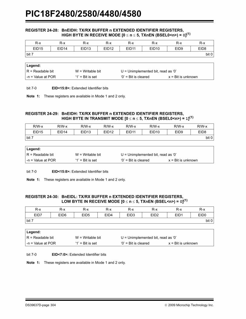
PIC18F2480/2580/4480/4580
REGISTER 24-28: BnEIDH: TX/RX BUFFER n EXTENDED IDENTIFIER REGISTERS, HIGH BYTE IN RECEIVE MODE [0 ≤ n ≤ 5, TXnEN (BSEL0<n>) = 0](1)
R-x R-x R-x R-x R-x R-x R-x R-xEID15 EID14 EID13 EID12 EID11 EID10 EID9 EID8
bit 7 bit 0
Legend:R = Readable bit W = Writable bit U = Unimplemented bit, read as ‘0’-n = Value at POR ‘1’ = Bit is set ‘0’ = Bit is cleared x = Bit is unknown
bit 7-0 EID<15:8>: Extended Identifier bits
Note 1: These registers are available in Mode 1 and 2 only.
REGISTER 24-29: BnEIDH: TX/RX BUFFER n EXTENDED IDENTIFIER REGISTERS, HIGH BYTE IN TRANSMIT MODE [0 ≤ n ≤ 5, TXnEN (BSEL0<n>) = 1](1)
R/W-x R/W-x R/W-x R/W-x R/W-x R/W-x R/W-x R/W-xEID15 EID14 EID13 EID12 EID11 EID10 EID9 EID8
bit 7 bit 0
Legend:R = Readable bit W = Writable bit U = Unimplemented bit, read as ‘0’-n = Value at POR ‘1’ = Bit is set ‘0’ = Bit is cleared x = Bit is unknown
bit 7-0 EID<15:8>: Extended Identifier bits
Note 1: These registers are available in Mode 1 and 2 only.
REGISTER 24-30: BnEIDL: TX/RX BUFFER n EXTENDED IDENTIFIER REGISTERS, LOW BYTE IN RECEIVE MODE [0 ≤ n ≤ 5, TXnEN (BSEL<n>) = 0](1)
R-x R-x R-x R-x R-x R-x R-x R-xEID7 EID6 EID5 EID4 EID3 EID2 EID1 EID0
bit 7 bit 0
Legend:R = Readable bit W = Writable bit U = Unimplemented bit, read as ‘0’-n = Value at POR ‘1’ = Bit is set ‘0’ = Bit is cleared x = Bit is unknown
bit 7-0 EID<7:0>: Extended Identifier bits
Note 1: These registers are available in Mode 1 and 2 only.
DS39637D-page 304 © 2009 Microchip Technology Inc.

PIC18F2480/2580/4480/4580
REGISTER 24-31: BnEIDL: TX/RX BUFFER n EXTENDED IDENTIFIER REGISTERS, LOW BYTE IN RECEIVE MODE [0 ≤ n ≤ 5, TXnEN (BSEL<n>) = 1](1)
R/W-x R/W-x R/W-x R/W-x R/W-x R/W-x R/W-x R/W-xEID7 EID6 EID5 EID4 EID3 EID2 EID1 EID0
bit 7 bit 0
Legend:R = Readable bit W = Writable bit U = Unimplemented bit, read as ‘0’-n = Value at POR ‘1’ = Bit is set ‘0’ = Bit is cleared x = Bit is unknown
bit 7-0 EID<7:0>: Extended Identifier bits
Note 1: These registers are available in Mode 1 and 2 only.
REGISTER 24-32: BnDm: TX/RX BUFFER n DATA FIELD BYTE m REGISTERS IN RECEIVE MODE[0 ≤ n ≤ 5, 0 ≤ m ≤ 7, TXnEN (BSEL<n>) = 0](1)
R-x R-x R-x R-x R-x R-x R-x R-xBnDm7 BnDm6 BnDm5 BnDm4 BnDm3 BnDm2 BnDm1 BnDm0
bit 7 bit 0
Legend:R = Readable bit W = Writable bit U = Unimplemented bit, read as ‘0’-n = Value at POR ‘1’ = Bit is set ‘0’ = Bit is cleared x = Bit is unknown
bit 7-0 BnDm<7:0>: Receive Buffer n Data Field Byte m bits (where 0 ≤ n < 3 and 0 < m < 8)Each receive buffer has an array of registers. For example, Receive Buffer 0 has 7 registers: B0D0 toB0D7.
Note 1: These registers are available in Mode 1 and 2 only.
REGISTER 24-33: BnDm: TX/RX BUFFER n DATA FIELD BYTE m REGISTERS IN TRANSMIT MODE[0 ≤ n ≤ 5, 0 ≤ m ≤ 7, TXnEN (BSEL<n>) = 1](1)
R/W-x R/W-x R/W-x R/W-x R/W-x R/W-x R/W-x R/W-xBnDm7 BnDm6 BnDm5 BnDm4 BnDm3 BnDm2 BnDm1 BnDm0
bit 7 bit 0
Legend:R = Readable bit W = Writable bit U = Unimplemented bit, read as ‘0’-n = Value at POR ‘1’ = Bit is set ‘0’ = Bit is cleared x = Bit is unknown
bit 7-0 BnDm<7:0>: Transmit Buffer n Data Field Byte m bits (where 0 ≤ n < 3 and 0 < m < 8)Each transmit buffer has an array of registers. For example, Transmit Buffer 0 has 7 registers: TXB0D0to TXB0D7.
Note 1: These registers are available in Mode 1 and 2 only.
© 2009 Microchip Technology Inc. DS39637D-page 305

PIC18F2480/2580/4480/4580
REGISTER 24-34: BnDLC: TX/RX BUFFER n DATA LENGTH CODE REGISTERS IN RECEIVE MODE[0 ≤ n ≤ 5, TXnEN (BSEL<n>) = 0](1)
U-0 R-x R-x R-x R-x R-x R-x R-x— RXRTR RB1 RB0 DLC3 DLC2 DLC1 DLC0
bit 7 bit 0
Legend:R = Readable bit W = Writable bit U = Unimplemented bit, read as ‘0’-n = Value at POR ‘1’ = Bit is set ‘0’ = Bit is cleared x = Bit is unknown
bit 7 Unimplemented: Read as ‘0’bit 6 RXRTR: Receiver Remote Transmission Request bit
1 = This is a remote transmission request0 = This is not a remote transmission request
bit 5 RB1: Reserved bit 1Reserved by CAN Spec and read as ‘0’.
bit 4 RB0: Reserved bit 0Reserved by CAN Spec and read as ‘0’.
bit 3-0 DLC<3:0>: Data Length Code bits1111 = Reserved 1110 = Reserved 1101 = Reserved 1100 = Reserved 1011 = Reserved 1010 = Reserved 1001 = Reserved 1000 = Data length = 8 bytes 0111 = Data length = 7 bytes 0110 = Data length = 6 bytes 0101 = Data length = 5 bytes 0100 = Data length = 4 bytes 0011 = Data length = 3 bytes 0010 = Data length = 2 bytes 0001 = Data length = 1 bytes 0000 = Data length = 0 bytes
Note 1: These registers are available in Mode 1 and 2 only.
DS39637D-page 306 © 2009 Microchip Technology Inc.

PIC18F2480/2580/4480/4580
REGISTER 24-35: BnDLC: TX/RX BUFFER n DATA LENGTH CODE REGISTERS IN TRANSMIT MODE[0 ≤ n ≤ 5, TXnEN (BSEL<n>) = 1](1)
U-0 R/W-x U-0 U-0 R/W-x R/W-x R/W-x R/W-x— TXRTR — — DLC3 DLC2 DLC1 DLC0
bit 7 bit 0
Legend:R = Readable bit W = Writable bit U = Unimplemented bit, read as ‘0’-n = Value at POR ‘1’ = Bit is set ‘0’ = Bit is cleared x = Bit is unknown
bit 7 Unimplemented: Read as ‘0’bit 6 TXRTR: Transmitter Remote Transmission Request bit
1 = Transmitted message will have RTR bit set0 = Transmitted message will have RTR bit cleared
bit 5-4 Unimplemented: Read as ‘0’bit 3-0 DLC<3:0>: Data Length Code bits
1111-1001 = Reserved 1000 = Data length = 8 bytes 0111 = Data length = 7 bytes 0110 = Data length = 6 bytes 0101 = Data length = 5 bytes 0100 = Data length = 4 bytes 0011 = Data length = 3 bytes 0010 = Data length = 2 bytes 0001 = Data length = 1 bytes 0000 = Data length = 0 bytes
Note 1: These registers are available in Mode 1 and 2 only.
REGISTER 24-36: BSEL0: BUFFER SELECT REGISTER 0(1)
R/W-0 R/W-0 R/W-0 R/W-0 R/W-0 R/W-0 U-0 U-0B5TXEN B4TXEN B3TXEN B2TXEN B1TXEN B0TXEN — —
bit 7 bit 0
Legend:R = Readable bit W = Writable bit U = Unimplemented bit, read as ‘0’-n = Value at POR ‘1’ = Bit is set ‘0’ = Bit is cleared x = Bit is unknown
bit 7-2 B5TXEN:B0TXEN: Buffer 5 to Buffer 0 Transmit Enable bit1 = Buffer is configured in Transmit mode0 = Buffer is configured in Receive mode
bit 1-0 Unimplemented: Read as ‘0’
Note 1: These registers are available in Mode 1 and 2 only.
© 2009 Microchip Technology Inc. DS39637D-page 307

PIC18F2480/2580/4480/4580
24.2.3.2 Message Acceptance Filtersand MasksThis section describes the message acceptance filtersand masks for the CAN receive buffers.
REGISTER 24-37: RXFnSIDH: RECEIVE ACCEPTANCE FILTER n STANDARD IDENTIFIER FILTER REGISTERS, HIGH BYTE [0 ≤ n ≤ 15](1)
R/W-x R/W-x R/W-x R/W-x R/W-x R/W-x R/W-x R/W-xSID10 SID9 SID8 SID7 SID6 SID5 SID4 SID3
bit 7 bit 0
Legend:R = Readable bit W = Writable bit U = Unimplemented bit, read as ‘0’-n = Value at POR ‘1’ = Bit is set ‘0’ = Bit is cleared x = Bit is unknown
bit 7-0 SID<10:3>: Standard Identifier Filter bits (if EXIDEN = 0)Extended Identifier Filter bits, EID<28:21> (if EXIDEN = 1).
Note 1: Registers, RXF6SIDH:RXF15SIDH, are available in Mode 1 and 2 only.
REGISTER 24-38: RXFnSIDL: RECEIVE ACCEPTANCE FILTER n STANDARD IDENTIFIER FILTER REGISTERS, LOW BYTE [0 ≤ n ≤ 15](1)
R/W-x R/W-x R/W-x U-0 R/W-x U-0 R/W-x R/W-xSID2 SID1 SID0 — EXIDEN(2) — EID17 EID16
bit 7 bit 0
Legend:R = Readable bit W = Writable bit U = Unimplemented bit, read as ‘0’-n = Value at POR ‘1’ = Bit is set ‘0’ = Bit is cleared x = Bit is unknown
bit 7-5 SID<2:0>: Standard Identifier Filter bits (if EXIDEN = 0)Extended Identifier Filter bits, EID<20:18> (if EXIDEN = 1).
bit 4 Unimplemented: Read as ‘0’bit 3 EXIDEN: Extended Identifier Filter Enable bit(2)
1 = Filter will only accept extended ID messages 0 = Filter will only accept standard ID messages
bit 2 Unimplemented: Read as ‘0’bit 1-0 EID<17:16>: Extended Identifier Filter bits
Note 1: Registers, RXF6SIDL:RXF15SIDL, are available in Mode 1 and 2 only.2: In Mode 0, this bit must be set/cleared as required, irrespective of corresponding mask register value.
DS39637D-page 308 © 2009 Microchip Technology Inc.

PIC18F2480/2580/4480/4580
REGISTER 24-39: RXFnEIDH: RECEIVE ACCEPTANCE FILTER n EXTENDED IDENTIFIERREGISTERS, HIGH BYTE [0 ≤ n ≤ 15](1)
R/W-x R/W-x R/W-x R/W-x R/W-x R/W-x R/W-x R/W-xEID15 EID14 EID13 EID12 EID11 EID10 EID9 EID8
bit 7 bit 0
Legend:R = Readable bit W = Writable bit U = Unimplemented bit, read as ‘0’-n = Value at POR ‘1’ = Bit is set ‘0’ = Bit is cleared x = Bit is unknown
bit 7-0 EID<15:8>: Extended Identifier Filter bits
Note 1: Registers, RXF6EIDH:RXF15EIDH, are available in Mode 1 and 2 only.
REGISTER 24-40: RXFnEIDL: RECEIVE ACCEPTANCE FILTER n EXTENDED IDENTIFIER REGISTERS, LOW BYTE [0 ≤ n ≤ 15](1)
R/W-x R/W-x R/W-x R/W-x R/W-x R/W-x R/W-x R/W-xEID7 EID6 EID5 EID4 EID3 EID2 EID1 EID0
bit 7 bit 0
Legend:R = Readable bit W = Writable bit U = Unimplemented bit, read as ‘0’-n = Value at POR ‘1’ = Bit is set ‘0’ = Bit is cleared x = Bit is unknown
bit 7-0 EID<7:0>: Extended Identifier Filter bits
Note 1: Registers, RXF6EIDL:RXF15EIDL, are available in Mode 1 and 2 only.
REGISTER 24-41: RXMnSIDH: RECEIVE ACCEPTANCE MASK n STANDARD IDENTIFIER MASK REGISTERS, HIGH BYTE [0 ≤ n ≤ 1]
R/W-x R/W-x R/W-x R/W-x R/W-x R/W-x R/W-x R/W-xSID10 SID9 SID8 SID7 SID6 SID5 SID4 SID3
bit 7 bit 0
Legend:R = Readable bit W = Writable bit U = Unimplemented bit, read as ‘0’-n = Value at POR ‘1’ = Bit is set ‘0’ = Bit is cleared x = Bit is unknown
bit 7-0 SID<10:3>: Standard Identifier Mask bits or Extended Identifier Mask bits (EID<28:21>)
© 2009 Microchip Technology Inc. DS39637D-page 309

PIC18F2480/2580/4480/4580
REGISTER 24-42: RXMnSIDL: RECEIVE ACCEPTANCE MASK n STANDARD IDENTIFIER MASK REGISTERS, LOW BYTE [0 ≤ n ≤ 1]
R/W-x R/W-x R/W-x U-0 R/W-0 U-0 R/W-x R/W-xSID2 SID1 SID0 — EXIDEN(1) — EID17 EID16
bit 7 bit 0
Legend:R = Readable bit W = Writable bit U = Unimplemented bit, read as ‘0’-n = Value at POR ‘1’ = Bit is set ‘0’ = Bit is cleared x = Bit is unknown
bit 7-5 SID<2:0>: Standard Identifier Mask bits or Extended Identifier Mask bits (EID<20:18>)bit 4 Unimplemented: Read as ‘0’bit 3 Mode 0:
Unimplemented: Read as ‘0’Mode 1, 2:EXIDEN: Extended Identifier Filter Enable Mask bit(1)
1 = Messages selected by the EXIDEN bit in RXFnSIDL will be accepted0 = Both standard and extended identifier messages will be accepted
bit 2 Unimplemented: Read as ‘0’bit 1-0 EID<17:16>: Extended Identifier Mask bits
Note 1: This bit is available in Mode 1 and 2 only.
REGISTER 24-43: RXMnEIDH: RECEIVE ACCEPTANCE MASK n EXTENDED IDENTIFIER MASK REGISTERS, HIGH BYTE [0 ≤ n ≤ 1]
R/W-x R/W-x R/W-x R/W-x R/W-x R/W-x R/W-x R/W-xEID15 EID14 EID13 EID12 EID11 EID10 EID9 EID8
bit 7 bit 0
Legend:R = Readable bit W = Writable bit U = Unimplemented bit, read as ‘0’-n = Value at POR ‘1’ = Bit is set ‘0’ = Bit is cleared x = Bit is unknown
bit 7-0 EID<15:8>: Extended Identifier Mask bits
REGISTER 24-44: RXMnEIDL: RECEIVE ACCEPTANCE MASK n EXTENDED IDENTIFIER MASK REGISTERS, LOW BYTE [0 ≤ n ≤ 1]
R/W-x R/W-x R/W-x R/W-x R/W-x R/W-x R/W-x R/W-xEID7 EID6 EID5 EID4 EID3 EID2 EID1 EID0
bit 7 bit 0
Legend:R = Readable bit W = Writable bit U = Unimplemented bit, read as ‘0’-n = Value at POR ‘1’ = Bit is set ‘0’ = Bit is cleared x = Bit is unknown
bit 7-0 EID<7:0>: Extended Identifier Mask bits
DS39637D-page 310 © 2009 Microchip Technology Inc.

PIC18F2480/2580/4480/4580
REGISTER 24-45: RXFCONn: RECEIVE FILTER CONTROL REGISTER n [0 ≤ n ≤ 1](1)
RXFCON0R/W-0 R/W-0 R/W-1 R/W-1 R/W-1 R/W-1 R/W-1 R/W-1
RXF7EN RXF6EN RXF5EN RXF4EN RXF3EN RXF2EN RXF1EN RXF0EN
RXFCON1R/W-0 R/W-0 R/W-0 R/W-1 R/W-0 R/W-0 R/W-0 R/W-0
RXF15EN RXF14EN RXF13EN RXF12EN RXF11EN RXF10EN RXF9EN RXF8ENbit 7 bit 0
Legend:R = Readable bit W = Writable bit U = Unimplemented bit, read as ‘0’-n = Value at POR ‘1’ = Bit is set ‘0’ = Bit is cleared x = Bit is unknown
bit 7-0 RXFnEN: Receive Filter n Enable bits0 = Filter is disabled1 = Filter is enabled
Note 1: This register is available in Mode 1 and 2 only.
Note: Register 24-46 through Register 24-51 are writable in Configuration mode only.
REGISTER 24-46: SDFLC: STANDARD DATA BYTES FILTER LENGTH COUNT REGISTER(1)
U-0 U-0 U-0 R/W-0 R/W-0 R/W-0 R/W-0 R/W-0— — — FLC4 FLC3 FLC2 FLC1 FLC0
bit 7 bit 0
Legend:R = Readable bit W = Writable bit U = Unimplemented bit, read as ‘0’-n = Value at POR ‘1’ = Bit is set ‘0’ = Bit is cleared x = Bit is unknown
bit 7-5 Unimplemented: Read as ‘0’bit 4-0 FLC<4:0>: Filter Length Count bits
Mode 0:Not used; forced to ‘00000’.00000-10010 = 0 18 bits are available for standard data byte filter. Actual number of bits used
depends on the DLC<3:0> bits (RXBnDLC<3:0> or BnDLC<3:0> if configuredas RX buffer) of the message being received.
If DLC<3:0> = 0000 No bits will be compared with incoming data bits.If DLC<3:0> = 0001 Up to 8 data bits of RXFnEID<7:0>, as determined by FLC<2:0>, will be com-
pared with the corresponding number of data bits of the incoming message.If DLC<3:0> = 0010 Up to 16 data bits of RXFnEID<15:0>, as determined by FLC<3:0>, will be
compared with the corresponding number of data bits of the incomingmessage.
If DLC<3:0> = 0011 Up to 18 data bits of RXFnEID<17:0>, as determined by FLC<4:0>, will becompared with the corresponding number of data bits of the incomingmessage.
Note 1: This register is available in Mode 1 and 2 only.
© 2009 Microchip Technology Inc. DS39637D-page 311

PIC18F2480/2580/4480/4580
REGISTER 24-47: RXFBCONn: RECEIVE FILTER BUFFER CONTROL REGISTER n(1)RXFBCON0R/W-0 R/W-0 R/W-0 R/W-0 R/W-0 R/W-0 R/W-0 R/W-0
F1BP_3 F1BP_2 F1BP_1 F1BP_0 F0BP_3 F0BP_2 F0BP_1 F0BP_0
RXFBCON1R/W-0 R/W-0 R/W-0 R/W-1 R/W-0 R/W-0 R/W-0 R/W-1
F3BP_3 F3BP_2 F3BP_1 F3BP_0 F2BP_3 F2BP_2 F2BP_1 F2BP_0
RXFBCON2R/W-0 R/W-0 R/W-0 R/W-1 R/W-0 R/W-0 R/W-0 R/W-1
F5BP_3 F5BP_2 F5BP_1 F5BP_0 F4BP_3 F4BP_2 F4BP_1 F4BP_0
RXFBCON3R/W-0 R/W-0 R/W-0 R/W-0 R/W-0 R/W-0 R/W-0 R/W-0
F7BP_3 F7BP_2 F7BP_1 F7BP_0 F6BP_3 F6BP_2 F6BP_1 F6BP_0
RXFBCON4R/W-0 R/W-0 R/W-0 R/W-0 R/W-0 R/W-0 R/W-0 R/W-0
F9BP_3 F9BP_2 F9BP_1 F9BP_0 F8BP_3 F8BP_2 F8BP_1 F8BP_0
RXFBCON5R/W-0 R/W-0 R/W-0 R/W-0 R/W-0 R/W-0 R/W-0 R/W-0
F11BP_3 F11BP_2 F11BP_1 F11BP_0 F10BP_3 F10BP_2 F10BP_1 F10BP_0
RXFBCON6R/W-0 R/W-0 R/W-0 R/W-0 R/W-0 R/W-0 R/W-0 R/W-0
F13BP_3 F13BP_2 F13BP_1 F13BP_0 F12BP_3 F12BP_2 F12BP_1 F12BP_0
RXFBCON7R/W-0 R/W-0 R/W-0 R/W-0 R/W-0 R/W-0 R/W-0 R/W-0
F15BP_3 F15BP_2 F15BP_1 F15BP_0 F14BP_3 F14BP_2 F14BP_1 F14BP_0bit 7 bit 0
Legend:R = Readable bit W = Writable bit U = Unimplemented bit, read as ‘0’-n = Value at POR ‘1’ = Bit is set ‘0’ = Bit is cleared x = Bit is unknown
bit 7-0 FnBP_<3:0>: Filter n Buffer Pointer Nibble bits0000 = Filter n is associated with RXB00001 = Filter n is associated with RXB10010 = Filter n is associated with B00011 = Filter n is associated with B1...0111 = Filter n is associated with B51111-1000 = Reserved
Note 1: This register is available in Mode 1 and 2 only.
DS39637D-page 312 © 2009 Microchip Technology Inc.

PIC18F2480/2580/4480/4580
REGISTER 24-48: MSEL0: MASK SELECT REGISTER 0(1)R/W-0 R/W-1 R/W-0 R/W-1 R/W-0 R/W-0 R/W-0 R/W-0FIL3_1 FIL3_0 FIL2_1 FIL2_0 FIL1_1 FIL1_0 FIL0_1 FIL0_0
bit 7 bit 0
Legend:R = Readable bit W = Writable bit U = Unimplemented bit, read as ‘0’-n = Value at POR ‘1’ = Bit is set ‘0’ = Bit is cleared x = Bit is unknown
bit 7-6 FIL3_<1:0>: Filter 3 Select bits 1 and 011 = No mask10 = Filter 1501 = Acceptance Mask 100 = Acceptance Mask 0
bit 5-4 FIL2_<1:0>: Filter 2 Select bits 1 and 011 = No mask10 = Filter 1501 = Acceptance Mask 100 = Acceptance Mask 0
bit 3-2 FIL1_<1:0>: Filter 1 Select bits 1 and 011 = No mask10 = Filter 1501 = Acceptance Mask 100 = Acceptance Mask 0
bit 1-0 FIL0_<1:0>: Filter 0 Select bits 1 and 011 = No mask10 = Filter 1501 = Acceptance Mask 100 = Acceptance Mask 0
Note 1: This register is available in Mode 1 and 2 only.
© 2009 Microchip Technology Inc. DS39637D-page 313

PIC18F2480/2580/4480/4580
REGISTER 24-49: MSEL1: MASK SELECT REGISTER 1(1)R/W-0 R/W-0 R/W-0 R/W-0 R/W-0 R/W-1 R/W-0 R/W-1FIL7_1 FIL7_0 FIL6_1 FIL6_0 FIL5_1 FIL5_0 FIL4_1 FIL4_0
bit 7 bit 0
Legend:R = Readable bit W = Writable bit U = Unimplemented bit, read as ‘0’-n = Value at POR ‘1’ = Bit is set ‘0’ = Bit is cleared x = Bit is unknown
bit 7-6 FIL7_<1:0>: Filter 7 Select bits 1 and 011 = No mask10 = Filter 1501 = Acceptance Mask 100 = Acceptance Mask 0
bit 5-4 FIL6_<1:0>: Filter 6 Select bits 1 and 011 = No mask10 = Filter 1501 = Acceptance Mask 100 = Acceptance Mask 0
bit 3-2 FIL5_<1:0>: Filter 5 Select bits 1 and 011 = No mask10 = Filter 1501 = Acceptance Mask 100 = Acceptance Mask 0
bit 1-0 FIL4_<1:0>: Filter 4 Select bits 1 and 011 = No mask10 = Filter 1501 = Acceptance Mask 100 = Acceptance Mask 0
Note 1: This register is available in Mode 1 and 2 only.
DS39637D-page 314 © 2009 Microchip Technology Inc.

PIC18F2480/2580/4480/4580
REGISTER 24-50: MSEL2: MASK SELECT REGISTER 2(1)R/W-0 R/W-0 R/W-0 R/W-0 R/W-0 R/W-0 R/W-0 R/W-0FIL11_1 FIL11_0 FIL10_1 FIL10_0 FIL9_1 FIL9_0 FIL8_1 FIL8_0
bit 7 bit 0
Legend:R = Readable bit W = Writable bit U = Unimplemented bit, read as ‘0’-n = Value at POR ‘1’ = Bit is set ‘0’ = Bit is cleared x = Bit is unknown
bit 7-6 FIL11_<1:0>: Filter 11 Select bits 1 and 011 = No mask10 = Filter 1501 = Acceptance Mask 100 = Acceptance Mask 0
bit 5-4 FIL10_<1:0>: Filter 10 Select bits 1 and 011 = No mask10 = Filter 1501 = Acceptance Mask 100 = Acceptance Mask 0
bit 3-2 FIL9_<1:0>: Filter 9 Select bits 1 and 011 = No mask10 = Filter 1501 = Acceptance Mask 100 = Acceptance Mask 0
bit 1-0 FIL8_<1:0>: Filter 8 Select bits 1 and 011 = No mask10 = Filter 1501 = Acceptance Mask 100 = Acceptance Mask 0
Note 1: This register is available in Mode 1 and 2 only.
© 2009 Microchip Technology Inc. DS39637D-page 315
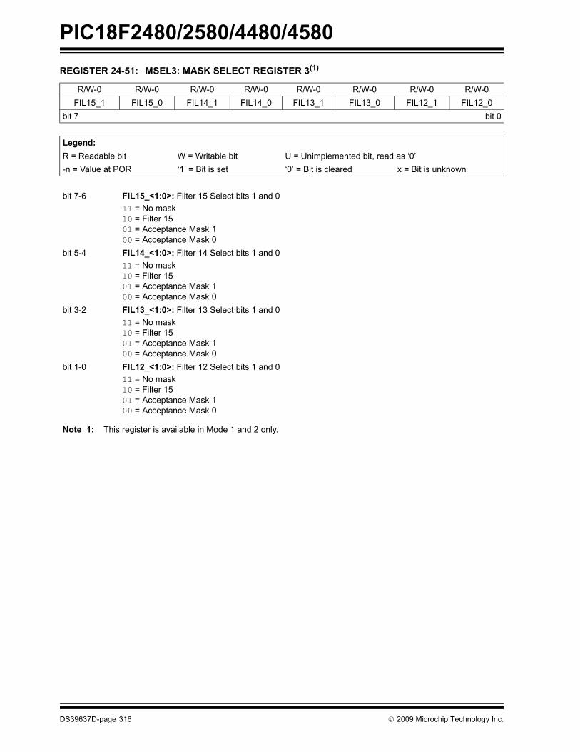
PIC18F2480/2580/4480/4580
REGISTER 24-51: MSEL3: MASK SELECT REGISTER 3(1)R/W-0 R/W-0 R/W-0 R/W-0 R/W-0 R/W-0 R/W-0 R/W-0FIL15_1 FIL15_0 FIL14_1 FIL14_0 FIL13_1 FIL13_0 FIL12_1 FIL12_0
bit 7 bit 0
Legend:R = Readable bit W = Writable bit U = Unimplemented bit, read as ‘0’-n = Value at POR ‘1’ = Bit is set ‘0’ = Bit is cleared x = Bit is unknown
bit 7-6 FIL15_<1:0>: Filter 15 Select bits 1 and 011 = No mask10 = Filter 1501 = Acceptance Mask 100 = Acceptance Mask 0
bit 5-4 FIL14_<1:0>: Filter 14 Select bits 1 and 011 = No mask10 = Filter 1501 = Acceptance Mask 100 = Acceptance Mask 0
bit 3-2 FIL13_<1:0>: Filter 13 Select bits 1 and 011 = No mask10 = Filter 1501 = Acceptance Mask 100 = Acceptance Mask 0
bit 1-0 FIL12_<1:0>: Filter 12 Select bits 1 and 011 = No mask10 = Filter 1501 = Acceptance Mask 100 = Acceptance Mask 0
Note 1: This register is available in Mode 1 and 2 only.
DS39637D-page 316 © 2009 Microchip Technology Inc.

PIC18F2480/2580/4480/4580
24.2.4 CAN BAUD RATE REGISTERSThis section describes the CAN Baud Rate registers.Note: These registers are writable inConfiguration mode only.
REGISTER 24-52: BRGCON1: BAUD RATE CONTROL REGISTER 1
R/W-0 R/W-0 R/W-0 R/W-0 R/W-0 R/W-0 R/W-0 R/W-0SJW1 SJW0 BRP5 BRP4 BRP3 BRP2 BRP1 BRP0
bit 7 bit 0
Legend:R = Readable bit W = Writable bit U = Unimplemented bit, read as ‘0’-n = Value at POR ‘1’ = Bit is set ‘0’ = Bit is cleared x = Bit is unknown
bit 7-6 SJW<1:0>: Synchronized Jump Width bits11 = Synchronization jump width time = 4 x TQ 10 = Synchronization jump width time = 3 x TQ 01 = Synchronization jump width time = 2 x TQ 00 = Synchronization jump width time = 1 x TQ
bit 5-0 BRP<5:0>: Baud Rate Prescaler bits111111 = TQ = (2 x 64)/FOSC 111110 = TQ = (2 x 63)/FOSC :
: 000001 = TQ = (2 x 2)/FOSC 000000 = TQ = (2 x 1)/FOSC
© 2009 Microchip Technology Inc. DS39637D-page 317

PIC18F2480/2580/4480/4580
REGISTER 24-53: BRGCON2: BAUD RATE CONTROL REGISTER 2R/W-0 R/W-0 R/W-0 R/W-0 R/W-0 R/W-0 R/W-0 R/W-0SEG2PHTS SAM SEG1PH2 SEG1PH1 SEG1PH0 PRSEG2 PRSEG1 PRSEG0
bit 7 bit 0
Legend:R = Readable bit W = Writable bit U = Unimplemented bit, read as ‘0’-n = Value at POR ‘1’ = Bit is set ‘0’ = Bit is cleared x = Bit is unknown
bit 7 SEG2PHTS: Phase Segment 2 Time Select bit1 = Freely programmable 0 = Maximum of PHEG1 or Information Processing Time (IPT), whichever is greater
bit 6 SAM: Sample of the CAN bus Line bit1 = Bus line is sampled three times prior to the sample point 0 = Bus line is sampled once at the sample point
bit 5-3 SEG1PH<2:0>: Phase Segment 1 bits111 = Phase Segment 1 time = 8 x TQ 110 = Phase Segment 1 time = 7 x TQ 101 = Phase Segment 1 time = 6 x TQ 100 = Phase Segment 1 time = 5 x TQ 011 = Phase Segment 1 time = 4 x TQ 010 = Phase Segment 1 time = 3 x TQ 001 = Phase Segment 1 time = 2 x TQ 000 = Phase Segment 1 time = 1 x TQ
bit 2-0 PRSEG<2:0>: Propagation Time Select bits111 = Propagation time = 8 x TQ 110 = Propagation time = 7 x TQ 101 = Propagation time = 6 x TQ 100 = Propagation time = 5 x TQ 011 = Propagation time = 4 x TQ 010 = Propagation time = 3 x TQ 001 = Propagation time = 2 x TQ 000 = Propagation time = 1 x TQ
DS39637D-page 318 © 2009 Microchip Technology Inc.

PIC18F2480/2580/4480/4580
REGISTER 24-54: BRGCON3: BAUD RATE CONTROL REGISTER 3R/W-0 R/W-0 U-0 U-0 U-0 R/W-0 R/W-0 R/W-0WAKDIS WAKFIL — — — SEG2PH2(1) SEG2PH1(1) SEG2PH0(1)
bit 7 bit 0
Legend:R = Readable bit W = Writable bit U = Unimplemented bit, read as ‘0’-n = Value at POR ‘1’ = Bit is set ‘0’ = Bit is cleared x = Bit is unknown
bit 7 WAKDIS: Wake-up Disable bit1 = Disable CAN bus activity wake-up feature0 = Enable CAN bus activity wake-up feature
bit 6 WAKFIL: Selects CAN bus Line Filter for Wake-up bit1 = Use CAN bus line filter for wake-up 0 = CAN bus line filter is not used for wake-up
bit 5-3 Unimplemented: Read as ‘0’bit 2-0 SEG2PH<2:0>: Phase Segment 2 Time Select bits(1)
111 = Phase Segment 2 time = 8 x TQ 110 = Phase Segment 2 time = 7 x TQ 101 = Phase Segment 2 time = 6 x TQ 100 = Phase Segment 2 time = 5 x TQ 011 = Phase Segment 2 time = 4 x TQ 010 = Phase Segment 2 time = 3 x TQ 001 = Phase Segment 2 time = 2 x TQ 000 = Phase Segment 2 time = 1 x TQ
Note 1: Ignored if SEG2PHTS bit (BRGCON2<7>) is ‘0’.
© 2009 Microchip Technology Inc. DS39637D-page 319

PIC18F2480/2580/4480/4580
24.2.5 CAN MODULE I/O CONTROLREGISTERThis register controls the operation of the CAN module’sI/O pins in relation to the rest of the microcontroller.
REGISTER 24-55: CIOCON: CAN I/O CONTROL REGISTER
U-0 U-0 R/W-0 R/W-0 U-0 U-0 U-0 U-0— — ENDRHI(1) CANCAP — — — —
bit 7 bit 0
Legend:R = Readable bit W = Writable bit U = Unimplemented bit, read as ‘0’-n = Value at POR ‘1’ = Bit is set ‘0’ = Bit is cleared x = Bit is unknown
bit 7-6 Unimplemented: Read as ‘0’bit 5 ENDRHI: Enable Drive High bit(1)
1 = CANTX pin will drive VDD when recessive 0 = CANTX pin will be tri-state when recessive
bit 4 CANCAP: CAN Message Receive Capture Enable bit1 = Enable CAN capture, CAN message receive signal replaces input on RC2/CCP1 0 = Disable CAN capture, RC2/CCP1 input to CCP1 module
bit 3-0 Unimplemented: Read as ‘0’
Note 1: Always set this bit when using a differential bus to avoid signal crosstalk in CANTX from other nearby pins.
DS39637D-page 320 © 2009 Microchip Technology Inc.

PIC18F2480/2580/4480/4580
24.2.6 CAN INTERRUPT REGISTERSThe registers in this section are the same as describedin Section 10.0 “Interrupts”. They are duplicated herefor convenience. REGISTER 24-56: PIR3: PERIPHERAL INTERRUPT REQUEST (FLAG) REGISTER 3Mode 0R/W-0 R/W-0 R/W-0 R/W-0 R/W-0 R/W-0 R/W-0 R/W-0IRXIF WAKIF ERRIF TXB2IF TXB1IF(1) TXB0IF(1) RXB1IF RXB0IF
Mode 1,2R/W-0 R/W-0 R/W-0 R/W-0 R/W-0 R/W-0 R/W-0 R/W-0IRXIF WAKIF ERRIF TXBnIF TXB1IF(1) TXB0IF(1) RXBnIF FIFOWMIF
bit 7 bit 0
Legend:R = Readable bit W = Writable bit U = Unimplemented bit, read as ‘0’-n = Value at POR ‘1’ = Bit is set ‘0’ = Bit is cleared x = Bit is unknown
bit 7 IRXIF: CAN Bus Error Message Received Interrupt Flag bit1 = An invalid message has occurred on the CAN bus 0 = No invalid message on CAN bus
bit 6 WAKIF: CAN Bus Activity Wake-up Interrupt Flag bit1 = Activity on CAN bus has occurred 0 = No activity on CAN bus
bit 5 ERRIF: CAN Module Error Interrupt Flag bit1 = An error has occurred in the CAN module (multiple sources; refer to Section 24.15.6 “Error Interrupt”)0 = No CAN module errors
bit 4 When CAN is in Mode 0:TXB2IF: CAN Transmit Buffer 2 Interrupt Flag bit1 = Transmit Buffer 2 has completed transmission of a message and may be reloaded 0 = Transmit Buffer 2 has not completed transmission of a messageWhen CAN is in Mode 1 or 2:TXBnIF: Any Transmit Buffer Interrupt Flag bit1 = One or more transmit buffers have completed transmission of a message and may be reloaded 0 = No transmit buffer is ready for reload
bit 3 TXB1IF: CAN Transmit Buffer 1 Interrupt Flag bit(1)
1 = Transmit Buffer 1 has completed transmission of a message and may be reloaded 0 = Transmit Buffer 1 has not completed transmission of a message
bit 2 TXB0IF: CAN Transmit Buffer 0 Interrupt Flag bit(1)
1 = Transmit Buffer 0 has completed transmission of a message and may be reloaded 0 = Transmit Buffer 0 has not completed transmission of a message
bit 1 When CAN is in Mode 0:RXB1IF: CAN Receive Buffer 1 Interrupt Flag bit1 = Receive Buffer 1 has received a new message 0 = Receive Buffer 1 has not received a new message When CAN is in Mode 1 or 2:RXBnIF: Any Receive Buffer Interrupt Flag bit1 = One or more receive buffers has received a new message 0 = No receive buffer has received a new message
bit 0 When CAN is in Mode 0:RXB0IF: CAN Receive Buffer 0 Interrupt Flag bit1 = Receive Buffer 0 has received a new message 0 = Receive Buffer 0 has not received a new messageWhen CAN is in Mode 1:Unimplemented: Read as ‘0’When CAN is in Mode 2:FIFOWMIF: FIFO Watermark Interrupt Flag bit1 = FIFO high watermark is reached 0 = FIFO high watermark is not reached
Note 1: In CAN Mode 1 and 2, these bits are forced to ‘0’.
© 2009 Microchip Technology Inc. DS39637D-page 321

PIC18F2480/2580/4480/4580
REGISTER 24-57: PIE3: PERIPHERAL INTERRUPT ENABLE REGISTER 3Mode 0R/W-0 R/W-0 R/W-0 R/W-0 R/W-0 R/W-0 R/W-0 R/W-0IRXIE WAKIE ERRIE TXB2IE TXB1IE(1) TXB0IE(1) RXB1IE RXB0IE
Mode 1R/W-0 R/W-0 R/W-0 R/W-0 R/W-0 R/W-0 R/W-0 R/W-0IRXIE WAKIE ERRIE TXBnIE TXB1IE(1) TXB0IE(1) RXBnIE FIFOWMIE
bit 7 bit 0
Legend:R = Readable bit W = Writable bit U = Unimplemented bit, read as ‘0’-n = Value at POR ‘1’ = Bit is set ‘0’ = Bit is cleared x = Bit is unknown
bit 7 IRXIE: CAN Bus Error Message Received Interrupt Enable bit1 = Enable invalid message received interrupt 0 = Disable invalid message received interrupt
bit 6 WAKIE: CAN bus Activity Wake-up Interrupt Enable bit1 = Enable bus activity wake-up interrupt 0 = Disable bus activity wake-up interrupt
bit 5 ERRIE: CAN bus Error Interrupt Enable bit1 = Enable CAN module error interrupt 0 = Disable CAN module error interrupt
bit 4 When CAN is in Mode 0:TXB2IE: CAN Transmit Buffer 2 Interrupt Enable bit1 = Enable Transmit Buffer 2 interrupt 0 = Disable Transmit Buffer 2 interruptWhen CAN is in Mode 1 or 2:TXBnIE: CAN Transmit Buffer Interrupts Enable bit1 = Enable transmit buffer interrupt; individual interrupt is enabled by TXBIE and BIE0 0 = Disable all transmit buffer interrupts
bit 3 TXB1IE: CAN Transmit Buffer 1 Interrupt Enable bit(1)
1 = Enable Transmit Buffer 1 interrupt 0 = Disable Transmit Buffer 1 interrupt
bit 2 TXB0IE: CAN Transmit Buffer 0 Interrupt Enable bit(1)
1 = Enable Transmit Buffer 0 interrupt 0 = Disable Transmit Buffer 0 interrupt
bit 1 When CAN is in Mode 0:RXB1IE: CAN Receive Buffer 1 Interrupt Enable bit1 = Enable Receive Buffer 1 interrupt 0 = Disable Receive Buffer 1 interrupt When CAN is in Mode 1 or 2:RXBnIE: CAN Receive Buffer Interrupts Enable bit1 = Enable receive buffer interrupt; individual interrupt is enabled by BIE0 0 = Disable all receive buffer interrupts
bit 0 When CAN is in Mode 0:RXB0IE: CAN Receive Buffer 0 Interrupt Enable bit1 = Enable Receive Buffer 0 interrupt 0 = Disable Receive Buffer 0 interrupt When CAN is in Mode 1:Unimplemented: Read as ‘0’When CAN is in Mode 2:FIFOWMIE: FIFO Watermark Interrupt Enable bit1 = Enable FIFO watermark interrupt 0 = Disable FIFO watermark interrupt
Note 1: In CAN Mode 1 and 2, these bits are forced to ‘0’.
DS39637D-page 322 © 2009 Microchip Technology Inc.

PIC18F2480/2580/4480/4580
REGISTER 24-58: IPR3: PERIPHERAL INTERRUPT PRIORITY REGISTER 3Mode 0R/W-1 R/W-1 R/W-1 R/W-1 R/W-1 R/W-1 R/W-1 R/W-1IRXIP WAKIP ERRIP TXB2IP TXB1IP(1) TXB0IP(1) RXB1IP RXB0IP
Mode 1,2R/W-1 R/W-1 R/W-1 R/W-1 R/W-1 R/W-1 R/W-1 R/W-1IRXIP WAKIP ERRIP TXBnIP TXB1IP(1) TXB0IP(1) RXBnIP FIFOWMIP
bit 7 bit 0
Legend:R = Readable bit W = Writable bit U = Unimplemented bit, read as ‘0’-n = Value at POR ‘1’ = Bit is set ‘0’ = Bit is cleared x = Bit is unknown
bit 7 IRXIP: CAN Bus Error Message Received Interrupt Priority bit1 = High priority 0 = Low priority
bit 6 WAKIP: CAN Bus Activity Wake-up Interrupt Priority bit1 = High priority 0 = Low priority
bit 5 ERRIP: CAN Module Error Interrupt Priority bit1 = High priority 0 = Low priority
bit 4 When CAN is in Mode 0:TXB2IP: CAN Transmit Buffer 2 Interrupt Priority bit1 = High priority 0 = Low priority When CAN is in Mode 1 or 2:TXBnIP: CAN Transmit Buffer Interrupt Priority bit1 = High priority 0 = Low priority
bit 3 TXB1IP: CAN Transmit Buffer 1 Interrupt Priority bit(1)
1 = High priority 0 = Low priority
bit 2 TXB0IP: CAN Transmit Buffer 0 Interrupt Priority bit(1)
1 = High priority 0 = Low priority
bit 1 When CAN is in Mode 0:RXB1IP: CAN Receive Buffer 1 Interrupt Priority bit1 = High priority 0 = Low priority When CAN is in Mode 1 or 2:RXBnIP: CAN Receive Buffer Interrupts Priority bit1 = High priority 0 = Low priority
bit 0 When CAN is in Mode 0:RXB0IP: CAN Receive Buffer 0 Interrupt Priority bit1 = High priority 0 = Low priority When CAN is in Mode 1:Unimplemented: Read as ‘0’When CAN is in Mode 2:FIFOWMIP: FIFO Watermark Interrupt Priority bit1 = High priority 0 = Low priority
Note 1: In CAN Mode 1 and 2, these bits are forced to ‘0’.
© 2009 Microchip Technology Inc. DS39637D-page 323

PIC18F2480/2580/4480/4580
REGISTER 24-59: TXBIE: TRANSMIT BUFFERS INTERRUPT ENABLE REGISTER(1)
U-0 U-0 U-0 R/W-0 R/W-0 R/W-0 U-0 U-0— — — TXB2IE(2) TXB1IE(2) TXB0IE(2) — —
bit 7 bit 0
Legend:R = Readable bit W = Writable bit U = Unimplemented bit, read as ‘0’-n = Value at POR ‘1’ = Bit is set ‘0’ = Bit is cleared x = Bit is unknown
bit 7-5 Unimplemented: Read as ‘0’bit 4-2 TXB2IE:TXB0IE: Transmit Buffer 2-0 Interrupt Enable bits(2)
1 = Transmit buffer interrupt is enabled0 = Transmit buffer interrupt is disabled
bit 1-0 Unimplemented: Read as ‘0’
Note 1: This register is available in Mode 1 and 2 only.2: TXBnIE in PIE3 register must be set to get an interrupt.
REGISTER 24-60: BIE0: BUFFER INTERRUPT ENABLE REGISTER 0(1)
R/W-0 R/W-0 R/W-0 R/W-0 R/W-0 R/W-0 R/W-0 R/W-0B5IE(2) B4IE(2) B3IE(2) B2IE(2) B1IE(2) B0IE(2) RXB1IE(2) RXB0IE(2)
bit 7 bit 0
Legend:R = Readable bit W = Writable bit U = Unimplemented bit, read as ‘0’-n = Value at POR ‘1’ = Bit is set ‘0’ = Bit is cleared x = Bit is unknown
bit 7-2 B5IE:B0IE: Programmable Transmit/Receive Buffer 5-0 Interrupt Enable bits(2)
1 = Interrupt is enabled0 = Interrupt is disabled
bit 1-0 RXB1IE:RXB0IE: Dedicated Receive Buffer 1-0 Interrupt Enable bits(2)
1 = Interrupt is enabled0 = Interrupt is disabled
Note 1: This register is available in Mode 1 and 2 only.2: Either TXBnIE or RXBnIE in the PIE3 register must be set to get an interrupt.
DS39637D-page 324 © 2009 Microchip Technology Inc.

PIC18F2480/2580/4480/4580
TABLE 24-1: CAN CONTROLLER REGISTER MAP
Address(1) Name Address Name Address Name Address NameF7Fh SPBRGH(3) F5Fh CANCON_RO0 F3Fh CANCON_RO2 F1Fh RXM1EIDLF7Eh BAUDCON(3) F5Eh CANSTAT_RO0 F3Eh CANSTAT_RO2 F1Eh RXM1EIDHF7Dh —(4) F5Dh RXB1D7 F3Dh TXB1D7 F1Dh RXM1SIDLF7Ch —(4) F5Ch RXB1D6 F3Ch TXB1D6 F1Ch RXM1SIDHF7Bh —(4) F5Bh RXB1D5 F3Bh TXB1D5 F1Bh RXM0EIDLF7Ah —(4) F5Ah RXB1D4 F3Ah TXB1D4 F1Ah RXM0EIDHF79h ECCP1DEL(3) F59h RXB1D3 F39h TXB1D3 F19h RXM0SIDLF78h —(4) F58h RXB1D2 F38h TXB1D2 F18h RXM0SIDHF77h ECANCON F57h RXB1D1 F37h TXB1D1 F17h RXF5EIDLF76h TXERRCNT F56h RXB1D0 F36h TXB1D0 F16h RXF5EIDHF75h RXERRCNT F55h RXB1DLC F35h TXB1DLC F15h RXF5SIDLF74h COMSTAT F54h RXB1EIDL F34h TXB1EIDL F14h RXF5SIDHF73h CIOCON F53h RXB1EIDH F33h TXB1EIDH F13h RXF4EIDLF72h BRGCON3 F52h RXB1SIDL F32h TXB1SIDL F12h RXF4EIDHF71h BRGCON2 F51h RXB1SIDH F31h TXB1SIDH F11h RXF4SIDLF70h BRGCON1 F50h RXB1CON F30h TXB1CON F10h RXF4SIDHF6Fh CANCON F4Fh CANCON_RO1(2) F2Fh CANCON_RO3(2) F0Fh RXF3EIDLF6Eh CANSTAT F4Eh CANSTAT_RO1(2) F2Eh CANSTAT_RO3(2) F0Eh RXF3EIDHF6Dh RXB0D7 F4Dh TXB0D7 F2Dh TXB2D7 F0Dh RXF3SIDLF6Ch RXB0D6 F4Ch TXB0D6 F2Ch TXB2D6 F0Ch RXF3SIDHF6Bh RXB0D5 F4Bh TXB0D5 F2Bh TXB2D5 F0Bh RXF2EIDLF6Ah RXB0D4 F4Ah TXB0D4 F2Ah TXB2D4 F0Ah RXF2EIDHF69h RXB0D3 F49h TXB0D3 F29h TXB2D3 F09h RXF2SIDLF68h RXB0D2 F48h TXB0D2 F28h TXB2D2 F08h RXF2SIDHF67h RXB0D1 F47h TXB0D1 F27h TXB2D1 F07h RXF1EIDLF66h RXB0D0 F46h TXB0D0 F26h TXB2D0 F06h RXF1EIDHF65h RXB0DLC F45h TXB0DLC F25h TXB2DLC F05h RXF1SIDLF64h RXB0EIDL F44h TXB0EIDL F24h TXB2EIDL F04h RXF1SIDHF63h RXB0EIDH F43h TXB0EIDH F23h TXB2EIDH F03h RXF0EIDLF62h RXB0SIDL F42h TXB0SIDL F22h TXB2SIDL F02h RXF0EIDHF61h RXB0SIDH F41h TXB0SIDH F21h TXB2SIDH F01h RXF0SIDLF60h RXB0CON F40h TXB0CON F20h TXB2CON F00h RXF0SIDH
Note 1: Shaded registers are available in Access Bank low area, while the rest are available in Bank 15.2: CANSTAT register is repeated in these locations to simplify application firmware. Unique names are given
for each instance of the controller register due to the Microchip header file requirement.3: These registers are not CAN registers.4: Unimplemented registers are read as ‘0’.
© 2009 Microchip Technology Inc. DS39637D-page 325

PIC18F2480/2580/4480/4580
EFFh —(4) EDFh —(4) EBFh —(4) E9Fh —(4)
EFEh —(4) EDEh —(4) EBEh —(4) E9Eh —(4)
EFDh —(4) EDDh —(4) EBDh —(4) E9Dh —(4)
EFCh —(4) EDCh —(4) EBCh —(4) E9Ch —(4)
EFBh —(4) EDBh —(4) EBBh —(4) E9Bh —(4)
EFAh —(4) EDAh —(4) EBAh —(4) E9Ah —(4)
EF9h —(4) ED9h —(4) EB9h —(4) E99h —(4)
EF8h —(4) ED8h —(4) EB8h —(4) E98h —(4)
EF7h —(4) ED7h —(4) EB7h —(4) E97h —(4)
EF6h —(4) ED6h —(4) EB6h —(4) E96h —(4)
EF5h —(4) ED5h —(4) EB5h —(4) E95h —(4)
EF4h —(4) ED4h —(4) EB4h —(4) E94h —(4)
EF3h —(4) ED3h —(4) EB3h —(4) E93h —(4)
EF2h —(4) ED2h —(4) EB2h —(4) E92h —(4)
EF1h —(4) ED1h —(4) EB1h —(4) E91h —(4)
EF0h —(4) ED0h —(4) EB0h —(4) E90h —(4)
EEFh —(4) ECFh —(4) EAFh —(4) E8Fh —(4)
EEEh —(4) ECEh —(4) EAEh —(4) E8Eh —(4)
EEDh —(4) ECDh —(4) EADh —(4) E8Dh —(4)
EECh —(4) ECCh —(4) EACh —(4) E8Ch —(4)
EEBh —(4) ECBh —(4) EABh —(4) E8Bh —(4)
EEAh —(4) ECAh —(4) EAAh —(4) E8Ah —(4)
EE9h —(4) EC9h —(4) EA9h —(4) E89h —(4)
EE8h —(4) EC8h —(4) EA8h —(4) E88h —(4)
EE7h —(4) EC7h —(4) EA7h —(4) E87h —(4)
EE6h —(4) EC6h —(4) EA6h —(4) E86h —(4)
EE5h —(4) EC5h —(4) EA5h —(4) E85h —(4)
EE4h —(4) EC4h —(4) EA4h —(4) E84h —(4)
EE3h —(4) EC3h —(4) EA3h —(4) E83h —(4)
EE2h —(4) EC2h —(4) EA2h —(4) E82h —(4)
EE1h —(4) EC1h —(4) EA1h —(4) E81h —(4)
EE0h —(4) EC0h —(4) EA0h —(4) E80h —(4)
TABLE 24-1: CAN CONTROLLER REGISTER MAP (CONTINUED)
Address(1) Name Address Name Address Name Address Name
Note 1: Shaded registers are available in Access Bank low area, while the rest are available in Bank 15.2: CANSTAT register is repeated in these locations to simplify application firmware. Unique names are given
for each instance of the controller register due to the Microchip header file requirement.3: These registers are not CAN registers.4: Unimplemented registers are read as ‘0’.
DS39637D-page 326 © 2009 Microchip Technology Inc.

PIC18F2480/2580/4480/4580
E7Fh CANCON_RO4(2) E5Fh CANCON_RO6(2) E3Fh CANCON_RO8(2) E1Fh —(4)
E7Eh CANSTAT_RO4(2) E5Eh CANSTAT_RO6(2) E3Eh CANSTAT_RO8(2) E1Eh —(4)
E7Dh B5D7 E5Dh B3D7 E3Dh B1D7 E1Dh —(4)
E7Ch B5D6 E5Ch B3D6 E3Ch B1D6 E1Ch —(4)
E7Bh B5D5 E5Bh B3D5 E3Bh B1D5 E1Bh —(4)
E7Ah B5D4 E5Ah B3D4 E3Ah B1D4 E1Ah —(4)
E79h B5D3 E59h B3D3 E39h B1D3 E19h —(4)
E78h B5D2 E58h B3D2 E38h B1D2 E18h —(4)
E77h B5D1 E57h B3D1 E37h B1D1 E17h —(4)
E76h B5D0 E56h B3D0 E36h B1D0 E16h —(4)
E75h B5DLC E55h B3DLC E35h B1DLC E15h —(4)
E74h B5EIDL E54h B3EIDL E34h B1EIDL E14h —(4)
E73h B5EIDH E53h B3EIDH E33h B1EIDH E13h —(4)
E72h B5SIDL E52h B3SIDL E32h B1SIDL E12h —(4)
E71h B5SIDH E51h B3SIDH E31h B1SIDH E11h —(4)
E70h B5CON E50h B3CON E30h B1CON E10h —(4)
E6Fh CANCON_RO5 E4Fh CANCON_RO7 E2Fh CANCON_RO9 E0Fh —(4)
E6Eh CANSTAT_RO5 E4Eh CANSTAT_RO7 E2Eh CANSTAT_RO9 E0Eh —(4)
E6Dh B4D7 E4Dh B2D7 E2Dh B0D7 E0Dh —(4)
E6Ch B4D6 E4Ch B2D6 E2Ch B0D6 E0Ch —(4)
E6Bh B4D5 E4Bh B2D5 E2Bh B0D5 E0Bh —(4)
E6Ah B4D4 E4Ah B2D4 E2Ah B0D4 E0Ah —(4)
E69h B4D3 E49h B2D3 E29h B0D3 E09h —(4)
E68h B4D2 E48h B2D2 E28h B0D2 E08h —(4)
E67h B4D1 E47h B2D1 E27h B0D1 E07h —(4)
E66h B4D0 E46h B2D0 E26h B0D0 E06h —(4)
E65h B4DLC E45h B2DLC E25h B0DLC E05h —(4)
E64h B4EIDL E44h B2EIDL E24h B0EIDL E04h —(4)
E63h B4EIDH E43h B2EIDH E23h B0EIDH E03h —(4)
E62h B4SIDL E42h B2SIDL E22h B0SIDL E02h —(4)
E61h B4SIDH E41h B2SIDH E21h B0SIDH E01h —(4)
E60h B4CON E40h B2CON E20h B0CON E00h —(4)
TABLE 24-1: CAN CONTROLLER REGISTER MAP (CONTINUED)
Address(1) Name Address Name Address Name Address Name
Note 1: Shaded registers are available in Access Bank low area, while the rest are available in Bank 15.2: CANSTAT register is repeated in these locations to simplify application firmware. Unique names are given
for each instance of the controller register due to the Microchip header file requirement.3: These registers are not CAN registers.4: Unimplemented registers are read as ‘0’.
© 2009 Microchip Technology Inc. DS39637D-page 327

PIC18F2480/2580/4480/4580
DFFh —(4) DDFh —(4) DBFh —(4) D9Fh —(4)
DFEh —(4) DDEh —(4) DBEh —(4) D9Eh —(4)
DFDh —(4) DDDh —(4) DBDh —(4) D9Dh —(4)
DFCh TXBIE DDCh —(4) DBCh —(4) D9Ch —(4)
DFBh —(4) DDBh —(4) DBBh —(4) D9Bh —(4)
DFAh BIE0 DDAh —(4) DBAh —(4) D9Ah —(4)
DF9h —(4) DD9h —(4) DB9h —(4) D99h —(4)
DF8h BSEL0 DD8h SDFLC DB8h —(4) D98h —(4)
DF7h —(4) DD7h —(4) DB7h —(4) D97h —(4)
DF6h —(4) DD6h —(4) DB6h —(4) D96h —(4)
DF5h —(4) DD5h RXFCON1 DB5h —(4) D95h —(4)
DF4h —(4) DD4h RXFCON0 DB4h —(4) D94h —(4)
DF3h MSEL3 DD3h —(4) DB3h —(4) D93h RXF15EIDLDF2h MSEL2 DD2h —(4) DB2h —(4) D92h RXF15EIDHDF1h MSEL1 DD1h —(4) DB1h —(4) D91h RXF15SIDLDF0h MSEL0 DD0h —(4) DB0h —(4) D90h RXF15SIDHDEFh —(4) DCFh —(4) DAFh —(4) D8Fh —(4)
DEEh —(4) DCEh —(4) DAEh —(4) D8Eh —(4)
DEDh —(4) DCDh —(4) DADh —(4) D8Dh —(4)
DECh —(4) DCCh —(4) DACh —(4) D8Ch —(4)
DEBh —(4) DCBh —(4) DABh —(4) D8Bh RXF14EIDLDEAh —(4) DCAh —(4) DAAh —(4) D8Ah RXF14EIDHDE9h —(4) DC9h —(4) DA9h —(4) D89h RXF14SIDLDE8h —(4) DC8h —(4) DA8h —(4) D88h RXF14SIDHDE7h RXFBCON7 DC7h —(4) DA7h —(4) D87h RXF13EIDLDE6h RXFBCON6 DC6h —(4) DA6h —(4) D86h RXF13EIDHDE5h RXFBCON5 DC5h —(4) DA5h —(4) D85h RXF13SIDLDE4h RXFBCON4 DC4h —(4) DA4h —(4) D84h RXF13SIDHDE3h RXFBCON3 DC3h —(4) DA3h —(4) D83h RXF12EIDLDE2h RXFBCON2 DC2h —(4) DA2h —(4) D82h RXF12EIDHDE1h RXFBCON1 DC1h —(4) DA1h —(4) D81h RXF12SIDLDE0h RXFBCON0 DC0h —(4) DA0h —(4) D80h RXF12SIDH
TABLE 24-1: CAN CONTROLLER REGISTER MAP (CONTINUED)
Address(1) Name Address Name Address Name Address Name
Note 1: Shaded registers are available in Access Bank low area, while the rest are available in Bank 15.2: CANSTAT register is repeated in these locations to simplify application firmware. Unique names are given
for each instance of the controller register due to the Microchip header file requirement.3: These registers are not CAN registers.4: Unimplemented registers are read as ‘0’.
DS39637D-page 328 © 2009 Microchip Technology Inc.

PIC18F2480/2580/4480/4580
TABLE 24-1: CAN CONTROLLER REGISTER MAP (CONTINUED)
Address(1) Name
D7Fh —(4)
D7Eh —(4)
D7Dh —(4)
D7Ch —(4)
D7Bh RXF11EIDLD7Ah RXF11EIDHD79h RXF11SIDLD78h RXF11SIDHD77h RXF10EIDLD76h RXF10EIDHD75h RXF10SIDLD74h RXF10SIDHD73h RXF9EIDLD72h RXF9EIDHD71h RXF9SIDLD70h RXF9SIDHD6Fh —(4)
D6Eh —(4)
D6Dh —(4)
D6Ch —(4)
D6Bh RXF8EIDLD6Ah RXF8EIDHD69h RXF8SIDLD68h RXF8SIDHD67h RXF7EIDLD66h RXF7EIDHD65h RXF7SIDLD64h RXF7SIDHD63h RXF6EIDLD62h RXF6EIDHD61h RXF6SIDLD60h RXF6SIDH
Note 1: Shaded registers are available in Access Bank low area while the rest are available in Bank 15.2: CANSTAT register is repeated in these locations to simplify application firmware. Unique names are given
for each instance of the controller register due to the Microchip header file requirement.3: These registers are not CAN registers.4: Unimplemented registers are read as ‘0’.
© 2009 Microchip Technology Inc. DS39637D-page 329

PIC18F2480/2580/4480/4580
24.3 CAN Modes of OperationThe PIC18F2480/2580/4480/4580 has six main modesof operation:• Configuration mode• Disable/Sleep mode• Normal Operation mode• Listen Only mode• Loopback mode• Error Recognition mode
All modes, except Error Recognition, are requested bysetting the REQOP bits (CANCON<7:5>). Error Recog-nition mode is requested through the RXM bits of theReceive Buffer register(s). Entry into a mode isAcknowledged by monitoring the OPMODE bits.
When changing modes, the mode will not actuallychange until all pending message transmissions arecomplete. Because of this, the user must verify that thedevice has actually changed into the requested modebefore further operations are executed.
24.3.1 CONFIGURATION MODEThe CAN module has to be initialized before theactivation. This is only possible if the module is in theConfiguration mode. The Configuration mode isrequested by setting the REQOP2 bit. Only when thestatus bit, OPMODE2, has a high level can the initial-ization be performed. Afterwards, the Configurationregisters, the acceptance mask registers and theacceptance filter registers can be written. The moduleis activated by setting the REQOP control bits to zero.
The module will protect the user from accidentallyviolating the CAN protocol through programmingerrors. All registers which control the configuration ofthe module can not be modified while the module is on-line. The CAN module will not be allowed to enter theConfiguration mode while a transmission or receptionis taking place. The Configuration mode serves as alock to protect the following registers:
• Configuration Registers • Functional Mode Selection Registers• Bit Timing Registers • Identifier Acceptance Filter Registers • Identifier Acceptance Mask Registers• Filter and Mask Control Registers• Mask Selection Registers
In the Configuration mode, the module will not transmitor receive. The error counters are cleared and the inter-rupt flags remain unchanged. The programmer willhave access to Configuration registers that are accessrestricted in other modes. I/O pins will revert to normalI/O functions.
24.3.2 DISABLE/SLEEP MODEIn Disable/Sleep mode, the module will not transmit orreceive. The module has the ability to set the WAKIF bitdue to bus activity; however, any pending interrupts willremain and the error counters will retain their value.
If the REQOP<2:0> bits are set to ‘001’, the module willenter the module Disable/Sleep mode. This mode issimilar to disabling other peripheral modules by turningoff the module enables. This causes the moduleinternal clock to stop unless the module is active (i.e.,receiving or transmitting a message). If the module isactive, the module will wait for 11 recessive bits on theCAN bus, detect that condition as an Idle bus, thenaccept the module Disable/Sleep command.OPMODE<2:0> = 001 indicates whether the modulesuccessfully went into the module Disable/Sleep mode.
The WAKIF interrupt is the only module interrupt that isstill active in the Disable/Sleep mode. If the WAKDIS iscleared and WAKIE is set, the processor will receive aninterrupt whenever the module detects recessive todominant transition. On wake-up, the module will auto-matically be set to the previous mode of operation. Forexample, if the module was switched from Normal toDisable/Sleep mode on bus activity wake-up, themodule will automatically enter into Normal mode andthe first message that caused the module to wake-up islost. The module will not generate any error frame.Firmware logic must detect this condition and makesure that retransmission is requested. If the processorreceives a wake-up interrupt while it is sleeping, morethan one message may get lost. The actual number ofmessages lost would depend on the processoroscillator start-up time and incoming message bit rate.
The TXCAN pin will stay in the recessive state while themodule is in Disable/Sleep mode.
24.3.3 NORMAL MODEThis is the standard operating mode of thePIC18F2480/2580/4480/4580 devices. In this mode,the device actively monitors all bus messages and gen-erates Acknowledge bits, error frames, etc. This is alsothe only mode in which the PIC18F2480/2580/4480/4580 devices will transmit messages over the CANbus.
DS39637D-page 330 © 2009 Microchip Technology Inc.

PIC18F2480/2580/4480/4580
24.3.4 LISTEN ONLY MODEListen Only mode provides a means for thePIC18F2480/2580/4480/4580 devices to receive allmessages, including messages with errors. This modecan be used for bus monitor applications or fordetecting the baud rate in ‘hot plugging’ situations. Forauto-baud detection, it is necessary that there are atleast two other nodes which are communicating witheach other. The baud rate can be detected empiricallyby testing different values until valid messages arereceived. The Listen Only mode is a silent mode,meaning no messages will be transmitted while in thisstate, including error flags or Acknowledge signals. Thefilters and masks can be used to allow only particularmessages to be loaded into the receive registers or thefilter masks can be set to all zeros to allow a messagewith any identifier to pass. The error counters are resetand deactivated in this state. The Listen Only mode isactivated by setting the mode request bits in theCANCON register.24.3.5 LOOPBACK MODEThis mode will allow internal transmission of messagesfrom the transmit buffers to the receive buffers withoutactually transmitting messages on the CAN bus. Thismode can be used in system development and testing.In this mode, the ACK bit is ignored and the device willallow incoming messages from itself, just as if theywere coming from another node. The Loopback modeis a silent mode, meaning no messages will be trans-mitted while in this state, including error flags orAcknowledge signals. The TXCAN pin will revert to portI/O while the device is in this mode. The filters andmasks can be used to allow only particular messagesto be loaded into the receive registers. The masks canbe set to all zeros to provide a mode that accepts allmessages. The Loopback mode is activated by settingthe mode request bits in the CANCON register.
24.3.6 ERROR RECOGNITION MODEThe module can be set to ignore all errors and receiveany message. In functional Mode 0, the Error Recogni-tion mode is activated by setting the RXM<1:0> bits inthe RXBnCON registers to ‘11’. In this mode, the datawhich is in the message assembly buffer until the errortime, is copied in the receive buffer and can be read viathe CPU interface.
24.4 CAN Module Functional ModesIn addition to CAN modes of operation, the ECAN mod-ule offers a total of 3 functional modes. Each of thesemodes are identified as Mode 0, Mode 1 and Mode 2.
24.4.1 MODE 0 – LEGACY MODEMode 0 is designed to be fully compatible with CANmodules used in PIC18CXX8 and PIC18FXX8 devices.This is the default mode of operation on all Reset con-ditions. As a result, module code written for thePIC18XX8 CAN module may be used on the ECANmodule without any code changes.
The following is the list of resources available in Mode 0:
• Three transmit buffers: TXB0, TXB1 and TXB2• Two receive buffers: RXB0 and RXB1• Two acceptance masks, one for each receive buf-
fer: RXM0, RXM1• Six acceptance filters, 2 for RXB0 and 4 for RXB1:
RXF0, RXF1, RXF2, RXF3, RXF4, RXF5
24.4.2 MODE 1 – ENHANCED LEGACY MODE
Mode 1 is similar to Mode 0, with the exceptionthat more resources are available in Mode 1. There are16 acceptance filters and two acceptance mask regis-ters. Acceptance Filter 15 can be used as either anacceptance filter or an acceptance mask register. Inaddition to three transmit and two receive buffers, thereare six more message buffers. One or more of theseadditional buffers can be programmed as transmit orreceive buffers. These additional buffers can also beprogrammed to automatically handle RTR messages.
Fourteen of sixteen acceptance filter registers can bedynamically associated to any receive buffer andacceptance mask register. One can use this capabilityto associate more than one filter to any one buffer.
When a receive buffer is programmed to use standardidentifier messages, part of the full acceptance filter reg-ister can be used as a data byte filter. The length of thedata byte filter is programmable from 0 to 18 bits. Thisfunctionality simplifies implementation of high-levelprotocols, such as the DeviceNet™ protocol.
The following is the list of resources available in Mode 1:
• Three transmit buffers: TXB0, TXB1 and TXB2• Two receive buffers: RXB0 and RXB1• Six buffers programmable as TX or RX: B0-B5• Automatic RTR handling on B0-B5• Sixteen dynamically assigned acceptance filters:
RXF0-RXF15• Two dedicated acceptance mask registers;
RXF15 programmable as third mask: RXM0-RXM1, RXF15
• Programmable data filter on standard identifier messages: SDFLC
© 2009 Microchip Technology Inc. DS39637D-page 331

PIC18F2480/2580/4480/4580
24.4.3 MODE 2 – ENHANCED FIFO MODEIn Mode 2, two or more receive buffers are used to formthe receive FIFO (first in, first out) buffer. There is noone-to-one relationship between the receive buffer andacceptance filter registers. Any filter that is enabled andlinked to any FIFO receive buffer can generateacceptance and cause FIFO to be updated.FIFO length is user-programmable, from 2-8 buffersdeep. FIFO length is determined by the very first pro-grammable buffer that is configured as a transmit buf-fer. For example, if Buffer 2 (B2) is programmed as atransmit buffer, FIFO consists of RXB0, RXB1, B0 andB1 – creating a FIFO length of 4. If all programmablebuffers are configured as receive buffers, FIFO willhave the maximum length of 8.
The following is the list of resources available in Mode 2:
• Three transmit buffers: TXB0, TXB1 and TXB2• Two receive buffers: RXB0 and RXB1• Six buffers programmable as TX or RX; receive
buffers form FIFO: B0-B5• Automatic RTR handling on B0-B5• Sixteen acceptance filters: RXF0-RXF15• Two dedicated acceptance mask registers;
RXF15 programmable as third mask: RXM0-RXM1, RXF15
• Programmable data filter on standard identifier messages: SDFLC, useful for DeviceNet protocol
24.5 CAN Message Buffers
24.5.1 DEDICATED TRANSMIT BUFFERSThe PIC18F2480/2580/4480/4580 devices implementthree dedicated transmit buffers – TXB0, TXB1 andTXB2. Each of these buffers occupies 14 bytes ofSRAM and are mapped into the SFR memory map.These are the only transmit buffers available inMode 0. Mode 1 and 2 may access these and otheradditional buffers.
Each transmit buffer contains one Control register(TXBnCON), four Identifier registers (TXBnSIDL,TXBnSIDH, TXBnEIDL, TXBnEIDH), one Data LengthCount register (TXBnDLC) and eight Data Byteregisters (TXBnDm).
24.5.2 DEDICATED RECEIVE BUFFERSThe PIC18F2480/2580/4480/4580 devices implementtwo dedicated receive buffers: RXB0 and RXB1. Eachof these buffers occupies 14 bytes of SRAM and aremapped into SFR memory map. These are the onlyreceive buffers available in Mode 0. Mode 1 and 2 mayaccess these and other additional buffers.
Each receive buffer contains one Control register(RXBnCON), four Identifier registers (RXBnSIDL,RXBnSIDH, RXBnEIDL, RXBnEIDH), one Data LengthCount register (RXBnDLC) and eight Data Byteregisters (RXBnDm).
There is also a separate Message Assembly Buffer(MAB) which acts as an additional receive buffer. MABis always committed to receiving the next messagefrom the bus and is not directly accessible to user firm-ware. The MAB assembles all incoming messages oneby one. A message is transferred to appropriatereceive buffers only if the corresponding acceptancefilter criteria is met.
24.5.3 PROGRAMMABLE TRANSMIT/RECEIVE BUFFERS
The ECAN module implements six new buffers: B0-B5.These buffers are individually programmable as eithertransmit or receive buffers. These buffers are availableonly in Mode 1 and 2. As with dedicated transmit andreceive buffers, each of these programmable buffersoccupies 14 bytes of SRAM and are mapped into SFRmemory map.
Each buffer contains one Control register (BnCON),four Identifier registers (BnSIDL, BnSIDH, BnEIDL,BnEIDH), one Data Length Count register (BnDLC)and eight Data Byte registers (BnDm). Each of theseregisters contains two sets of control bits. Dependingon whether the buffer is configured as transmit orreceive, one would use the corresponding control bitset. By default, all buffers are configured as receivebuffers. Each buffer can be individually configured as atransmit or receive buffer by setting the correspondingTXENn bit in the BSEL0 register.
When configured as transmit buffers, user firmwaremay access transmit buffers in any order similar toaccessing dedicated transmit buffers. In receiveconfiguration with Mode 1 enabled, user firmware mayalso access receive buffers in any order required. Butin Mode 2, all receive buffers are combined to form asingle FIFO. Actual FIFO length is programmable byuser firmware. Access to FIFO must be done throughthe FIFO Pointer bits (FP<4:0>) in the CANCONregister. It must be noted that there is no hardwareprotection against out of order FIFO reads.
DS39637D-page 332 © 2009 Microchip Technology Inc.
PIC18F2480/2580/4480/4580
24.5.4 PROGRAMMABLE AUTO-RTRBUFFERSIn Mode 1 and 2, any of six programmable transmit/receive buffers may be programmed to automaticallyrespond to predefined RTR messages without userfirmware intervention. Automatic RTR handling isenabled by setting the TXnEN bit in the BSEL0 registerand the RTREN bit in the BnCON register. After thissetup, when an RTR request is received, the TXREQbit is automatically set and the current buffer content isautomatically queued for transmission as a RTRresponse. As with all transmit buffers, once the TXREQbit is set, buffer registers become read-only and anywrites to them will be ignored.
The following outlines the steps required toautomatically handle RTR messages:
1. Set buffer to Transmit mode by setting theTXnEN bit to ‘1’ in BSEL0 register.
2. At least one acceptance filter must be associ-ated with this buffer and preloaded with theexpected RTR identifier.
3. Bit, RTREN in the BnCON register, must be setto ‘1’.
4. Buffer must be preloaded with the data to besent as a RTR response.
Normally, user firmware will keep buffer data registersup to date. If firmware attempts to update the bufferwhile an automatic RTR response is in the process oftransmission, all writes to buffers are ignored.
24.6 CAN Message Transmission
24.6.1 INITIATING TRANSMISSION For the MCU to have write access to the message buf-fer, the TXREQ bit must be clear, indicating that themessage buffer is clear of any pending message to betransmitted. At a minimum, the SIDH, SIDL and DLCregisters must be loaded. If data bytes are present inthe message, the Data registers must also be loaded.If the message is to use extended identifiers, theEIDH:EIDL registers must also be loaded and theEXIDE bit set.
To initiate message transmission, the TXREQ bit mustbe set for each buffer to be transmitted. When TXREQis set, the TXABT, TXLARB and TXERR bits will becleared. To successfully complete the transmission,there must be at least one node with matching baudrate on the network.
Setting the TXREQ bit does not initiate a messagetransmission; it merely flags a message buffer as readyfor transmission. Transmission will start when thedevice detects that the bus is available. The device willthen begin transmission of the highest priority messagethat is ready.
When the transmission has completed successfully, theTXREQ bit will be cleared, the TXBnIF bit will be set andan interrupt will be generated if the TXBnIE bit is set.
If the message transmission fails, the TXREQ will remainset, indicating that the message is still pending for trans-mission and one of the following condition flags will beset. If the message started to transmit but encounteredan error condition, the TXERR and the IRXIF bits will beset and an interrupt will be generated. If the message lostarbitration, the TXLARB bit will be set.
24.6.2 ABORTING TRANSMISSIONThe MCU can request to abort a message by clearingthe TXREQ bit associated with the corresponding mes-sage buffer (TXBnCON<3> or BnCON<3>). Setting theABAT bit (CANCON<4>) will request an abort of allpending messages. If the message has not yet startedtransmission, or if the message started but is inter-rupted by loss of arbitration or an error, the abort will beprocessed. The abort is indicated when the modulesets the TXABT bit for the corresponding buffer(TXBnCON<6> or BnCON<6>). If the message hasstarted to transmit, it will attempt to transmit the currentmessage fully. If the current message is transmittedfully and is not lost to arbitration or an error, the TXABTbit will not be set because the message was transmit-ted successfully. Likewise, if a message is being trans-mitted during an abort request and the message is lostto arbitration or an error, the message will not beretransmitted and the TXABT bit will be set, indicatingthat the message was successfully aborted.
Once an abort is requested by setting the ABAT orTXABT bits, it cannot be cleared to cancel the abortrequest. Only CAN module hardware or a PORcondition can clear it.
© 2009 Microchip Technology Inc. DS39637D-page 333

PIC18F2480/2580/4480/4580
24.6.3 TRANSMIT PRIORITYTransmit priority is a prioritization within thePIC18F2480/2580/4480/4580 devices of the pendingtransmittable messages. This is independent from andnot related to any prioritization implicit in the messagearbitration scheme built into the CAN protocol. Prior tosending the Start-Of-Frame (SOF), the priority of allbuffers that are queued for transmission is compared.The transmit buffer with the highest priority will be sentfirst. If two buffers have the same priority setting, thebuffer with the highest buffer number will be sent first.There are four levels of transmit priority. If the TXP bitsfor a particular message buffer are set to ‘11’, that buf-fer has the highest possible priority. If the TXP bits fora particular message buffer are set to ‘00’, that bufferhas the lowest possible priority.
FIGURE 24-2: TRANSMIT BUFFERS
TXR
EQ
TXB0
TXAB
T
TXLA
RB
TXER
R
TXB0
IF
MES
SAG
E
MessageQueueControl Transmit Byte Sequencer
TXR
EQ
TXB1TX
ABT
TXLA
RB
TXER
R
TXB1
IF
MES
SAG
E
TXR
EQ
TXB2
TXAB
T
TXLA
RB
TXER
R
TXB2
IF
MES
SAG
E
MES
SAG
E
TXB2
IF
TXR
EQ
TXAB
T
TXLA
RB
TXER
R
TXB3 - TXB8
DS39637D-page 334 © 2009 Microchip Technology Inc.

PIC18F2480/2580/4480/4580
24.7 Message Reception24.7.1 RECEIVING A MESSAGEOf all receive buffers, the MAB is always committed toreceiving the next message from the bus. The MCUcan access one buffer while the other buffer is availablefor message reception or holding a previously receivedmessage.
When a message is moved into either of the receivebuffers, the associated RXFUL bit is set. This bit mustbe cleared by the MCU when it has completed process-ing the message in the buffer in order to allow a newmessage to be received into the buffer. This bitprovides a positive lockout to ensure that the firmwarehas finished with the message before the moduleattempts to load a new message into the receive buffer.If the receive interrupt is enabled, an interrupt will begenerated to indicate that a valid message has beenreceived.
Once a message is loaded into any matching buffer,user firmware may determine exactly what filter causedthis reception by checking the filter hit bits in theRXBnCON or BnCON registers. In Mode 0,FILHIT<3:0> of RXBnCON serve as filter hit bits. InMode 1 and 2, FILHIT<4:0> bits of BnCON serve as fil-ter hit bits. The same registers also indicate whetherthe current message is an RTR frame or not. Areceived message is considered a standard identifiermessage if the EXID bit in the RXBnSIDL or theBnSIDL register is cleared. Conversely, a set EXID bitindicates an extended identifier message. If thereceived message is a standard identifier message,user firmware needs to read the SIDL and SIDH regis-ters. In the case of an extended identifier message,firmware should read the SIDL, SIDH, EIDL and EIDHregisters. If the RXBnDLC or BnDLC register containnon-zero data count, user firmware should also readthe corresponding number of data bytes by accessingthe RXBnDm or the BnDm registers. When a receivedmessage is an RTR and if the current buffer is not con-figured for automatic RTR handling, user firmwaremust take appropriate action and respond manually.
Each receive buffer contains RXM bits to set specialReceive modes. In Mode 0, RXM<1:0> bits inRXBnCON define a total of four Receive modes. InMode 1 and 2, RXM1 bit, in combination with the EXIDmask and filter bit, define the same four receive modes.
Normally, these bits are set to ‘00’ to enable receptionof all valid messages as determined by the appropriateacceptance filters. In this case, the determination ofwhether or not to receive standard or extended mes-sages is determined by the EXIDE bit in the accep-tance filter register. In Mode 0, if the RXM bits are setto ‘01’ or ‘10’, the receiver will accept only messageswith standard or extended identifiers, respectively. If anacceptance filter has the EXIDE bit set such that it doesnot correspond with the RXM mode, that acceptancefilter is rendered useless. In Mode 1 and 2, settingEXID in the SIDL Mask register will ensure that onlystandard or extended identifiers are received. Thesetwo modes of RXM bits can be used in systems whereit is known that only standard or extended messageswill be on the bus. If the RXM bits are set to ‘11’ (RXM1= 1 in Mode 1 and 2), the buffer will receive all mes-sages regardless of the values of the acceptance fil-ters. Also, if a message has an error before the end offrame, that portion of the message assembled in theMAB before the error frame will be loaded into the buf-fer. This mode may serve as a valuable debugging toolfor a given CAN network. It should not be used in anactual system environment as the actual system willalways have some bus errors and all nodes on the busare expected to ignore them.
In Mode 1 and 2, when a programmable buffer isconfigured as a transmit buffer and one or more accep-tance filters are associated with it, all incoming messagesmatching this acceptance filter criteria will be discarded.To avoid this scenario, user firmware must make surethat there are no acceptance filters associated with abuffer configured as a transmit buffer.
24.7.2 RECEIVE PRIORITYWhen in Mode 0, RXB0 is the higher priority buffer andhas two message acceptance filters associated with it.RXB1 is the lower priority buffer and has four acceptancefilters associated with it. The lower number of acceptancefilters makes the match on RXB0 more restrictive andimplies a higher priority for that buffer. Additionally, theRXB0CON register can be configured such that if RXB0contains a valid message and another valid message isreceived, an overflow error will not occur and the newmessage will be moved into RXB1 regardless of theacceptance criteria of RXB1. There are also twoprogrammable acceptance filter masks available, one foreach receive buffer (see Section 24.5 “CAN MessageBuffers”).
In Mode 1 and 2, there are a total of 16 acceptancefilters available and each can be dynamically assignedto any of the receive buffers. A buffer with a lowernumber has higher priority. Given this, if an incomingmessage matches with two or more receive bufferacceptance criteria, the buffer with the lower numberwill be loaded with that message.
Note: The entire contents of the MAB are movedinto the receive buffer once a message isaccepted. This means that regardless ofthe type of identifier (standard orextended) and the number of data bytesreceived, the entire receive buffer is over-written with the MAB contents. Therefore,the contents of all registers in the buffermust be assumed to have been modifiedwhen any message is received.
© 2009 Microchip Technology Inc. DS39637D-page 335

PIC18F2480/2580/4480/4580
24.7.3 ENHANCED FIFO MODEWhen configured for Mode 2, two of the dedicatedreceive buffers in combination with one or more pro-grammable transmit/receive buffers, are used to createa maximum of an 8 buffer deep FIFO buffer. In thismode, there is no direct correlation between filters andreceive buffer registers. Any filter that has beenenabled can generate an acceptance. When a mes-sage has been accepted, it is stored in the next avail-able receive buffer register and an internal WritePointer is incremented. The FIFO can be a maximumof 8 buffers deep. The entire FIFO must consist of con-tiguous receive buffers. The FIFO head begins atRXB0 buffer and its tail spans toward B5. The maxi-mum length of the FIFO is limited by the presence orabsence of the first transmit buffer starting from B0. If abuffer is configured as a transmit buffer, the FIFOlength is reduced accordingly. For instance, if B3 isconfigured as a transmit buffer, the actual FIFO willconsist of RXB0, RXB1, B0, B1 and B2, a total of 5 buf-fers. If B0 is configured as a transmit buffer, the FIFOlength will be 2. If none of the programmable buffersare configured as a transmit buffer, the FIFO will be8 buffers deep. A system that requires more transmitbuffers should try to locate transmit buffers at the veryend of B0-B5 buffers to maximize available FIFOlength.When a message is received in FIFO mode, the inter-rupt flag code bits (EICODE<4:0>) in the CANSTATregister will have a value of ‘10000’, indicating theFIFO has received a message. FIFO Pointer bits,FP<3:0> in the CANCON register, point to the bufferthat contains data not yet read. The FIFO Pointer bits,in this sense, serve as the FIFO Read Pointer. The usershould use FP bits and read corresponding buffer data.When receive data is no longer needed, the RXFUL bitin the current buffer must be cleared, causing FP<3:0>to be updated by the module.
To determine whether FIFO is empty or not, the usermay use the FP<3:0> bits to access the RXFUL bit inthe current buffer. If RXFUL is cleared, the FIFO is con-sidered to be empty. If it is set, the FIFO may containone or more messages. In Mode 2, the module alsoprovides a bit called FIFO High Water Mark (FIFOWM)in the ECANCON register. This bit can be used tocause an interrupt whenever the FIFO contains onlyone or four empty buffers. The FIFO high water markinterrupt can serve as an early warning to a full FIFOcondition.
24.7.4 TIME-STAMPINGThe CAN module can be programmed to generate atime-stamp for every message that is received. Whenenabled, the module generates a capture signal forCCP1, which in turn captures the value of either Timer1or Timer3. This value can be used as the messagetime-stamp.
To use the time-stamp capability, the CANCAP bit(CIOCON<4>) must be set. This replaces the captureinput for CCP1 with the signal generated from the CANmodule. In addition, CCP1CON<3:0> must be set to‘0011’ to enable the CCP Special Event Trigger forCAN events.
24.8 Message Acceptance Filters and Masks
The message acceptance filters and masks are used todetermine if a message in the Message Assembly Buf-fer should be loaded into any of the receive buffers.Once a valid message has been received into the MAB,the identifier fields of the message are compared to thefilter values. If there is a match, that message will beloaded into the appropriate receive buffer. The filtermasks are used to determine which bits in the identifierare examined with the filters. A truth table is shownbelow in Table 24-2 that indicates how each bit in theidentifier is compared to the masks and filters to deter-mine if a message should be loaded into a receive buf-fer. The mask essentially determines which bits toapply the acceptance filters to. If any mask bit is set toa zero, then that bit will automatically be acceptedregardless of the filter bit.
TABLE 24-2: FILTER/MASK TRUTH TABLE
In Mode 0, acceptance filters, RXF0 and RXF1, andfilter mask, RXM0, are associated with RXB0. Filters,RXF2, RXF3, RXF4 and RXF5, and mask, RXM1, areassociated with RXB1.
Mask bit n
Filter bit n
Message Identifier bit n001
Accept or Reject bit n
0 x x Accept1 0 0 Accept1 0 1 Reject1 1 0 Reject1 1 1 Accept
Legend: x = don’t care
DS39637D-page 336 © 2009 Microchip Technology Inc.

PIC18F2480/2580/4480/4580
In Mode 1 and 2, there are an additional 10 acceptancefilters, RXF6-RXF15, creating a total of 16 availablefilters. RXF15 can be used either as an acceptancefilter or acceptance mask register. Each of theseacceptance filters can be individually enabled ordisabled by setting or clearing the RXFENn bit in theRXFCONn register. Any of these 16 acceptance filterscan be dynamically associated with any of the receivebuffers. Actual association is made by setting theappropriate bits in the RXFBCONn register. EachRXFBCONn register contains a nibble for each filter.This nibble can be used to associate a specific filter toany of available receive buffers. User firmware mayassociate more than one filter to any one specificreceive buffer.In addition to dynamic filter to buffer association, inMode 1 and 2, each filter can also be dynamically asso-ciated to available Acceptance Mask registers. TheFILn_m bits in the MSELn register can be used to linka specific acceptance filter to an acceptance mask reg-ister. As with filter to buffer association, one can alsoassociate more than one mask to a specific acceptancefilter.
When a filter matches and a message is loaded into thereceive buffer, the filter number that enabled the mes-sage reception is loaded into the FILHIT bit(s). InMode 0 for RXB1, the RXB1CON register contains theFILHIT<2:0> bits. They are coded as follows:
• 101 = Acceptance Filter 5 (RXF5)• 100 = Acceptance Filter 4 (RXF4)• 011 = Acceptance Filter 3 (RXF3)• 010 = Acceptance Filter 2 (RXF2)• 001 = Acceptance Filter 1 (RXF1)• 000 = Acceptance Filter 0 (RXF0)
The coding of the RXB0DBEN bit enables these threebits to be used similarly to the FILHIT bits and to distin-guish a hit on filter, RXF0 and RXF1, in either RXB0 orafter a rollover into RXB1.
• 111 = Acceptance Filter 1 (RXF1)• 110 = Acceptance Filter 0 (RXF0)• 001 = Acceptance Filter 1 (RXF1)• 000 = Acceptance Filter 0 (RXF0)
If the RXB0DBEN bit is clear, there are six codescorresponding to the six filters. If the RXB0DBEN bit isset, there are six codes corresponding to the six filters,plus two additional codes corresponding to RXF0 andRXF1 filters, that rollover into RXB1.
In Mode 1 and 2, each buffer control register contains5 bits of filter hit bits (FILHIT<4:0>). A binary value of ‘0’indicates a hit from RXF0 and 15 indicates RXF15.
If more than one acceptance filter matches, the FILHITbits will encode the binary value of the lowest num-bered filter that matched. In other words, if filter RXF2and filter RXF4 match, FILHIT will be loaded with thevalue for RXF2. This essentially prioritizes theacceptance filters with a lower number filter havinghigher priority. Messages are compared to filters inascending order of filter number.
The mask and filter registers can only be modifiedwhen the PIC18F2480/2580/4480/4580 devices are inConfiguration mode.
FIGURE 24-3: MESSAGE ACCEPTANCE MASK AND FILTER OPERATION
Note: ‘000’ and ‘001’ can only occur if theRXB0DBEN bit is set in the RXB0CONregister, allowing RXB0 messages torollover into RXB1.
Acceptance Filter Register Acceptance Mask Register
RxRqst
Message Assembly Buffer
RXFn0
RXFn1
RXFnn
RXMn0
RXMn1
RXMnn
Identifier
© 2009 Microchip Technology Inc. DS39637D-page 337

PIC18F2480/2580/4480/4580
24.9 Baud Rate SettingAll nodes on a given CAN bus must have the samenominal bit rate. The CAN protocol uses Non-Return-to-Zero (NRZ) coding which does not encode a clockwithin the data stream. Therefore, the receive clockmust be recovered by the receiving nodes andsynchronized to the transmitter’s clock.As oscillators and transmission time may vary fromnode to node, the receiver must have some type ofPhase Lock Loop (PLL) synchronized to data transmis-sion edges to synchronize and maintain the receiverclock. Since the data is NRZ coded, it is necessary toinclude bit stuffing to ensure that an edge occurs atleast every six bit times to maintain the Digital PhaseLock Loop (DPLL) synchronization.
The bit timing of the PIC18F2480/2580/4480/4580 isimplemented using a DPLL that is configured to syn-chronize to the incoming data and provides the nominaltiming for the transmitted data. The DPLL breaks eachbit time into multiple segments made up of minimalperiods of time called the Time Quanta (TQ).
Bus timing functions executed within the bit time frame,such as synchronization to the local oscillator, networktransmission delay compensation and sample pointpositioning, are defined by the programmable bit timinglogic of the DPLL.
All devices on the CAN bus must use the same bit rate.However, all devices are not required to have the samemaster oscillator clock frequency. For the different clockfrequencies of the individual devices, the bit rate has tobe adjusted by appropriately setting the baud rateprescaler and number of time quanta in each segment.
The Nominal Bit Rate is the number of bits transmittedper second, assuming an ideal transmitter with an idealoscillator, in the absence of resynchronization. Thenominal bit rate is defined to be a maximum of 1 Mb/s.
The Nominal Bit Time is defined as:
EQUATION 24-1:
The Nominal Bit Time can be thought of as beingdivided into separate, non-overlapping time segments.These segments (Figure 24-4) include:
• Synchronization Segment (Sync_Seg)• Propagation Time Segment (Prop_Seg)• Phase Buffer Segment 1 (Phase_Seg1)• Phase Buffer Segment 2 (Phase_Seg2)
The time segments (and thus, the Nominal Bit Time)are, in turn, made up of integer units of time called TimeQuanta or TQ (see Figure 24-4). By definition, theNominal Bit Time is programmable from a minimum of8 TQ to a maximum of 25 TQ. Also by definition, theminimum Nominal Bit Time is 1 μs, corresponding to amaximum 1 Mb/s rate. The actual duration is given bythe following relationship.
EQUATION 24-2:
The Time Quantum is a fixed unit derived from theoscillator period. It is also defined by the programmablebaud rate prescaler, with integer values from 1 to 64, inaddition to a fixed divide-by-two for clock generation.Mathematically, this is:
EQUATION 24-3:
where FOSC is the clock frequency, TOSC is thecorresponding oscillator period and BRP is an integer(0 through 63) represented by the binary values ofBRGCON1<5:0>. The equation above refers to theeffective clock frequency used by the microcontroller. If,for example, a 10 MHz crystal in HS mode is used, thenFOSC = 10 MHz and TOSC = 100 ns. If the same 10 MHzcrystal is used in HS-PLL mode, then the effectivefrequency is FOSC = 40 MHz and TOSC = 25 ns.
FIGURE 24-4: BIT TIME PARTITIONING
TBIT = 1/Nominal Bit Rate
Nominal Bit Time = TQ * (Sync_Seg + Prop_Seg +Phase_Seg1 + Phase_Seg2)
TQ (μs) = (2 * (BRP+1))/FOSC (MHz)or
TQ (μs) = (2 * (BRP+1)) * TOSC (μs)
Input
Sync PropagationSegment
PhaseSegment 1
PhaseSegment 2
Sample Point
TQ
Nominal Bit Time
BitTimeIntervals
Signal
SegmentSync
DS39637D-page 338 © 2009 Microchip Technology Inc.

PIC18F2480/2580/4480/4580
24.9.1 EXTERNAL CLOCK, INTERNALCLOCK AND MEASURABLE JITTER IN HS-PLL BASED OSCILLATORS
The microcontroller clock frequency generated from aPLL circuit is subject to a jitter, also defined as PhaseJitter or Phase Skew. For its PIC18 Enhanced micro-controllers, Microchip specifies phase jitter (Pjitter) asbeing 2% (Gaussian distribution, within 3 standarddeviations, see parameter F13 in Table 28-7) and TotalJitter (Tjitter) as being 2*Pjitter.
The CAN protocol uses a bit-stuffing technique thatinserts a bit of a given polarity following five bits with theopposite polarity. This gives a total of 10 bits transmit-ted without re-synchronization (compensation for jitteror phase error).
Given the random nature of the jitter error added, it canbe shown that the total error caused by the jitter tendsto cancel itself over time. For a period of 10 bits, it isnecessary to add only two jitter intervals to correct forjitter-induced error: one interval in the beginning of the10-bit period and another at the end. The overall effectis shown in Figure 24-5.
FIGURE 24-5: EFFECTS OF PHASE JITTER ON THE MICROCONTROLLER CLOCK AND CAN BIT TIME
Once these considerations are taken into account, it ispossible to show that the relation between the jitter andthe total frequency error can be defined as:
where jitter is expressed in terms of time and NBT is theNominal Bit Time.
For example, assume a CAN bit rate of 125 Kb/s, whichgives an NBT of 8 µs. For a 16 MHz clock generatedfrom a 4x PLL, the jitter at this clock frequency is:
and resultant frequency error is:
Nominal Clock
Clock with Jitter
CAN Bit Time
Phase Skew (Jitter)
CAN Bit Jitterwith Jitter
ΔfTjitter
10 NBT×------------------------
2 Pjitter×10 NBT×------------------------== 2% 1
16 MHz-------------------× 0.0216 6×10----------------- 1.25ns= =
2 1.25 9–×10( )×
10 8 6–×10( )×--------------------------------------- 3.125 5–×10 0.0031%==
© 2009 Microchip Technology Inc. DS39637D-page 339

PIC18F2480/2580/4480/4580
Table 24-3 shows the relation between the clockgenerated by the PLL and the frequency error fromjitter (measured jitter-induced error of 2%, Gaussiandistribution, within 3 standard deviations), as apercentage of the nominal clock frequency.This is clearly smaller than the expected drift of acrystal oscillator, typically specified at 100 ppm or0.01%. If we add jitter to oscillator drift, we have a totalfrequency drift of 0.0132%. The total oscillatorfrequency errors for common clock frequencies and bitrates, including both drift and jitter, are shown inTable 24-4.
TABLE 24-3: FREQUENCY ERROR FROM JITTER AT VARIOUS PLL-GENERATED CLOCK SPEEDS
TABLE 24-4: TOTAL FREQUENCY ERROR AT VARIOUS PLL-GENERATED CLOCK SPEEDS (100 PPM OSCILLATOR DRIFT, INCLUDING ERROR FROM JITTER)
PLL Output Pjitter Tjitter
Frequency Error at Various Nominal Bit Times (Bit Rates)
8 μs(125 Kb/s)
4 μs(250 Kb/s)
2 μs(500 Kb/s)
1 μs(1 Mb/s)
40 MHz 0.5 ns 1 ns 0.00125% 0.00250% 0.005% 0.01%24 MHz 0.83 ns 1.67 ns 0.00209% 0.00418% 0.008% 0.017%16 MHz 1.25 ns 2.5 ns 0.00313% 0.00625% 0.013% 0.025%
Nominal PLL OutputFrequency Error at Various Nominal Bit Times (Bit Rates)
8 μs(125 Kb/s)
4 μs(250 Kb/s)
2 μs(500 Kb/s)
1 μs(1 Mb/s)
40 MHz 0.01125% 0.01250% 0.015% 0.02%24 MHz 0.01209% 0.01418% 0.018% 0.027%16 MHz 0.01313% 0.01625% 0.023% 0.035%
DS39637D-page 340 © 2009 Microchip Technology Inc.
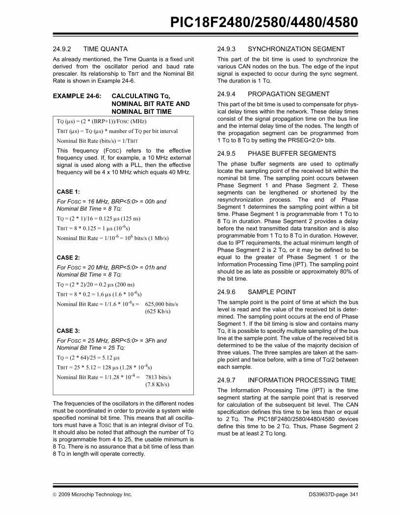
PIC18F2480/2580/4480/4580
24.9.2 TIME QUANTAAs already mentioned, the Time Quanta is a fixed unitderived from the oscillator period and baud rateprescaler. Its relationship to TBIT and the Nominal BitRate is shown in Example 24-6.EXAMPLE 24-6: CALCULATING TQ, NOMINAL BIT RATE AND NOMINAL BIT TIME
The frequencies of the oscillators in the different nodesmust be coordinated in order to provide a system widespecified nominal bit time. This means that all oscilla-tors must have a TOSC that is an integral divisor of TQ.It should also be noted that although the number of TQis programmable from 4 to 25, the usable minimum is8 TQ. There is no assurance that a bit time of less than8 TQ in length will operate correctly.
24.9.3 SYNCHRONIZATION SEGMENTThis part of the bit time is used to synchronize thevarious CAN nodes on the bus. The edge of the inputsignal is expected to occur during the sync segment.The duration is 1 TQ.
24.9.4 PROPAGATION SEGMENT This part of the bit time is used to compensate for phys-ical delay times within the network. These delay timesconsist of the signal propagation time on the bus lineand the internal delay time of the nodes. The length ofthe propagation segment can be programmed from1 TQ to 8 TQ by setting the PRSEG<2:0> bits.
24.9.5 PHASE BUFFER SEGMENTSThe phase buffer segments are used to optimallylocate the sampling point of the received bit within thenominal bit time. The sampling point occurs betweenPhase Segment 1 and Phase Segment 2. Thesesegments can be lengthened or shortened by theresynchronization process. The end of PhaseSegment 1 determines the sampling point within a bittime. Phase Segment 1 is programmable from 1 TQ to8 TQ in duration. Phase Segment 2 provides a delaybefore the next transmitted data transition and is alsoprogrammable from 1 TQ to 8 TQ in duration. However,due to IPT requirements, the actual minimum length ofPhase Segment 2 is 2 TQ, or it may be defined to beequal to the greater of Phase Segment 1 or theInformation Processing Time (IPT). The sampling pointshould be as late as possible or approximately 80% ofthe bit time.
24.9.6 SAMPLE POINTThe sample point is the point of time at which the buslevel is read and the value of the received bit is deter-mined. The sampling point occurs at the end of PhaseSegment 1. If the bit timing is slow and contains manyTQ, it is possible to specify multiple sampling of the busline at the sample point. The value of the received bit isdetermined to be the value of the majority decision ofthree values. The three samples are taken at the sam-ple point and twice before, with a time of TQ/2 betweeneach sample.
24.9.7 INFORMATION PROCESSING TIMEThe Information Processing Time (IPT) is the timesegment starting at the sample point that is reservedfor calculation of the subsequent bit level. The CANspecification defines this time to be less than or equalto 2 TQ. The PIC18F2480/2580/4480/4580 devicesdefine this time to be 2 TQ. Thus, Phase Segment 2must be at least 2 TQ long.
TQ (μs) = (2 * (BRP+1))/FOSC (MHz)
TBIT (μs) = TQ (μs) * number of TQ per bit interval
Nominal Bit Rate (bits/s) = 1/TBIT
This frequency (FOSC) refers to the effectivefrequency used. If, for example, a 10 MHz externalsignal is used along with a PLL, then the effectivefrequency will be 4 x 10 MHz which equals 40 MHz.
CASE 1:For FOSC = 16 MHz, BRP<5:0> = 00h and Nominal Bit Time = 8 TQ:
TQ = (2 * 1)/16 = 0.125 μs (125 ns)
TBIT = 8 * 0.125 = 1 μs (10-6s)
Nominal Bit Rate = 1/10-6 = 106 bits/s (1 Mb/s)
CASE 2:For FOSC = 20 MHz, BRP<5:0> = 01h and Nominal Bit Time = 8 TQ:
TQ = (2 * 2)/20 = 0.2 μs (200 ns)
TBIT = 8 * 0.2 = 1.6 μs (1.6 * 10-6s)
Nominal Bit Rate = 1/1.6 * 10-6s = 625,000 bits/s(625 Kb/s)
CASE 3:For FOSC = 25 MHz, BRP<5:0> = 3Fh and Nominal Bit Time = 25 TQ:
TQ = (2 * 64)/25 = 5.12 μs
TBIT = 25 * 5.12 = 128 μs (1.28 * 10-4s)
Nominal Bit Rate = 1/1.28 * 10-4 = 7813 bits/s(7.8 Kb/s)
© 2009 Microchip Technology Inc. DS39637D-page 341

PIC18F2480/2580/4480/4580
24.10 SynchronizationTo compensate for phase shifts between the oscillatorfrequencies of each of the nodes on the bus, each CANcontroller must be able to synchronize to the relevantsignal edge of the incoming signal. When an edge inthe transmitted data is detected, the logic will comparethe location of the edge to the expected time(Sync_Seg). The circuit will then adjust the values ofPhase Segment 1 and Phase Segment 2 as necessary.There are two mechanisms used for synchronization.24.10.1 HARD SYNCHRONIZATIONHard synchronization is only done when there is arecessive to dominant edge during a bus Idle condition,indicating the start of a message. After hard synchroni-zation, the bit time counters are restarted withSync_Seg. Hard synchronization forces the edge,which has occurred to lie within the synchronizationsegment of the restarted bit time. Due to the rules ofsynchronization, if a hard synchronization occurs, therewill not be a resynchronization within that bit time.
24.10.2 RESYNCHRONIZATIONAs a result of resynchronization, Phase Segment 1may be lengthened or Phase Segment 2 may be short-ened. The amount of lengthening or shortening of thephase buffer segments has an upper bound given bythe Synchronization Jump Width (SJW). The value ofthe SJW will be added to Phase Segment 1 (seeFigure 24-6) or subtracted from Phase Segment 2 (seeFigure 24-7). The SJW is programmable between 1 TQand 4 TQ.
Clocking information will only be derived from reces-sive to dominant transitions. The property, that only afixed maximum number of successive bits have thesame value, ensures resynchronization to the bitstream during a frame.
The phase error of an edge is given by the position ofthe edge relative to Sync_Seg, measured in TQ. Thephase error is defined in magnitude of TQ as follows:
• e = 0 if the edge lies within Sync_Seg.• e > 0 if the edge lies before the sample point.• e < 0 if the edge lies after the sample point of the
previous bit.
If the magnitude of the phase error is less than, or equalto, the programmed value of the Synchronization JumpWidth, the effect of a resynchronization is the same asthat of a hard synchronization.
If the magnitude of the phase error is larger than theSynchronization Jump Width and if the phase error ispositive, then Phase Segment 1 is lengthened by anamount equal to the Synchronization Jump Width.
If the magnitude of the phase error is larger than theresynchronization jump width and if the phase error isnegative, then Phase Segment 2 is shortened by anamount equal to the Synchronization Jump Width.
24.10.3 SYNCHRONIZATION RULES• Only one synchronization within one bit time is
allowed.• An edge will be used for synchronization only if
the value detected at the previous sample point (previously read bus value) differs from the bus value immediately after the edge.
• All other recessive to dominant edges fulfilling rules 1 and 2 will be used for resynchronization, with the exception that a node transmitting a dominant bit will not perform a resynchronization as a result of a recessive to dominant edge with a positive phase error.
DS39637D-page 342 © 2009 Microchip Technology Inc.

PIC18F2480/2580/4480/4580
FIGURE 24-6: LENGTHENING A BIT PERIOD (ADDING SJW TO PHASE SEGMENT 1)FIGURE 24-7: SHORTENING A BIT PERIOD (SUBTRACTING SJW FROM PHASE SEGMENT 2)
24.11 Programming Time SegmentsSome requirements for programming of the timesegments:
• Prop_Seg + Phase_Seg 1 ≥ Phase_Seg 2• Phase_Seg 2 ≥ Sync Jump Width.
For example, assume that a 125 kHz CAN baud rate isdesired, using 20 MHz for FOSC. With a TOSC of 50 ns,a baud rate prescaler value of 04h gives a TQ of 500 ns.To obtain a Nominal Bit Rate of 125 kHz, the NominalBit Time must be 8 μs or 16 TQ.
Using 1 TQ for the Sync_Seg, 2 TQ for the Prop_Segand 7 TQ for Phase Segment 1 would place the samplepoint at 10 TQ after the transition. This leaves 6 TQ forPhase Segment 2.
By the rules above, the Sync Jump Width could be themaximum of 4 TQ. However, normally a large SJW isonly necessary when the clock generation of thedifferent nodes is inaccurate or unstable, such as usingceramic resonators. Typically, an SJW of 1 is enough.
24.12 Oscillator ToleranceAs a rule of thumb, the bit timing requirements allowceramic resonators to be used in applications withtransmission rates of up to 125 Kbit/sec. For the full busspeed range of the CAN protocol, a quartz oscillator isrequired. Refer to ISO11898-1 for oscillator tolerancerequirements.
Input
SyncProp
SegmentPhase
Segment 1Phase
Segment 2≤ SJW
Sample PointTQ
Signal
Nominal Bit Length
Actual Bit Length
BitTimeSegments
SyncProp
SegmentPhase
Segment 1Phase
Segment 2 ≤ SJW
TQ Sample Point
Nominal Bit Length
Actual Bit Length
© 2009 Microchip Technology Inc. DS39637D-page 343

PIC18F2480/2580/4480/4580
24.13 Bit Timing ConfigurationRegistersThe Baud Rate Control registers (BRGCON1,BRGCON2, BRGCON3) control the bit timing for theCAN bus interface. These registers can only be modi-fied when the PIC18F2480/2580/4480/4580 devicesare in Configuration mode.
24.13.1 BRGCON1The BRP bits control the baud rate prescaler. TheSJW<1:0> bits select the synchronization jump width interms of multiples of TQ.
24.13.2 BRGCON2The PRSEG bits set the length of the propagation seg-ment in terms of TQ. The SEG1PH bits set the length ofPhase Segment 1 in TQ. The SAM bit controls howmany times the RXCAN pin is sampled. Setting this bitto a ‘1’ causes the bus to be sampled three times: twiceat TQ/2 before the sample point and once at the normalsample point (which is at the end of Phase Segment 1).The value of the bus is determined to be the value readduring at least two of the samples. If the SAM bit is setto a ‘0’, then the RXCAN pin is sampled only once atthe sample point. The SEG2PHTS bit controls how thelength of Phase Segment 2 is determined. If this bit isset to a ‘1’, then the length of Phase Segment 2 isdetermined by the SEG2PH bits of BRGCON3. If theSEG2PHTS bit is set to a ‘0’, then the length of PhaseSegment 2 is the greater of Phase Segment 1 and theinformation processing time (which is fixed at 2 TQ forthe PIC18F2480/2580/4480/4580).
24.13.3 BRGCON3The PHSEG2<2:0> bits set the length (in TQ) of PhaseSegment 2 if the SEG2PHTS bit is set to a ‘1’. If theSEG2PHTS bit is set to a ‘0’, then the PHSEG2<2:0>bits have no effect.
24.14 Error DetectionThe CAN protocol provides sophisticated errordetection mechanisms. The following errors can bedetected.
24.14.1 CRC ERRORWith the Cyclic Redundancy Check (CRC), the trans-mitter calculates special check bits for the bitsequence, from the start of a frame until the end of thedata field. This CRC sequence is transmitted in theCRC field. The receiving node also calculates the CRCsequence using the same formula and performs acomparison to the received sequence. If a mismatch isdetected, a CRC error has occurred and an error frameis generated. The message is repeated.
24.14.2 ACKNOWLEDGE ERRORIn the Acknowledge field of a message, the transmitterchecks if the Acknowledge slot (which was sent out asa recessive bit) contains a dominant bit. If not, no othernode has received the frame correctly. An Acknowl-edge error has occurred, an error frame is generatedand the message will have to be repeated.
24.14.3 FORM ERROR If a node detects a dominant bit in one of the four seg-ments, including End-Of-Frame (EOF), interframespace, Acknowledge delimiter or CRC delimiter, then aform error has occurred and an error frame isgenerated. The message is repeated.
24.14.4 BIT ERRORA bit error occurs if a transmitter sends a dominant bitand detects a recessive bit, or if it sends a recessive bitand detects a dominant bit, when monitoring the actualbus level and comparing it to the just transmitted bit. Inthe case where the transmitter sends a recessive bitand a dominant bit is detected during the arbitrationfield and the Acknowledge slot, no bit error isgenerated because normal arbitration is occurring.
24.14.5 STUFF BIT ERRORlf, between the Start-Of-Frame (SOF) and the CRCdelimiter, six consecutive bits with the same polarity aredetected, the bit stuffing rule has been violated. A stuffbit error occurs and an error frame is generated. Themessage is repeated.
24.14.6 ERROR STATESDetected errors are made public to all other nodes viaerror frames. The transmission of the erroneous mes-sage is aborted and the frame is repeated as soon aspossible. Furthermore, each CAN node is in one of thethree error states; “error-active”, “error-passive” or“bus-off”, according to the value of the internal errorcounters. The error-active state is the usual statewhere the bus node can transmit messages and acti-vate error frames (made of dominant bits) without anyrestrictions. In the error-passive state, messages andpassive error frames (made of recessive bits) may betransmitted. The bus-off state makes it temporarilyimpossible for the node to participate in the buscommunication. During this state, messages can neitherbe received nor transmitted.
24.14.7 ERROR MODES AND ERROR COUNTERS
The PIC18F2480/2580/4480/4580 devices contain twoerror counters: the Receive Error Counter (RXERRCNT)and the Transmit Error Counter (TXERRCNT). Thevalues of both counters can be read by the MCU. Thesecounters are incremented or decremented inaccordance with the CAN bus specification.
DS39637D-page 344 © 2009 Microchip Technology Inc.

PIC18F2480/2580/4480/4580
The PIC18F2480/2580/4480/4580 devices are error-active if both error counters are below the error-passivelimit of 128. They are error-passive if at least one of theerror counters equals or exceeds 128. They go to bus-off if the transmit error counter equals or exceeds thebus-off limit of 256. The devices remain in this stateuntil the bus-off recovery sequence is finished. Thebus-off recovery sequence consists of 128 occurrencesof 11 consecutive recessive bits (see Figure 24-8).Note that the CAN module, after going bus-off, willrecover back to error-active without any intervention bythe MCU if the bus remains Idle for 128 x 11 bit times.If this is not desired, the error Interrupt Service Routineshould address this. The current Error mode of theCAN module can be read by the MCU via theCOMSTAT register.
Additionally, there is an Error State Warning flag bit,EWARN, which is set if at least one of the error coun-ters equals or exceeds the error warning limit of 96.EWARN is reset if both error counters are less than theerror warning limit.
FIGURE 24-8: ERROR MODES STATE DIAGRAM
24.15 CAN InterruptsThe module has several sources of interrupts. Each ofthese interrupts can be individually enabled or dis-abled. The PIR3 register contains interrupt flags. ThePIE3 register contains the enables for the 8 main inter-rupts. A special set of read-only bits in the CANSTATregister, the ICODE bits, can be used in combinationwith a jump table for efficient handling of interrupts.
All interrupts have one source, with the exception of theerror interrupt and buffer interrupts in Mode 1 and 2. Anyof the error interrupt sources can set the error interruptflag. The source of the error interrupt can be determinedby reading the Communication Status register,COMSTAT. In Mode 1 and 2, there are two interruptenable/disable and flag bits – one for all transmit buffersand the other for all receive buffers.
The interrupts can be broken up into two categories:receive and transmit interrupts.
The receive related interrupts are:
• Receive Interrupts • Wake-up Interrupt • Receiver Overrun Interrupt• Receiver Warning Interrupt• Receiver Error-Passive Interrupt
The transmit related interrupts are:
• Transmit Interrupts • Transmitter Warning Interrupt • Transmitter Error-Passive Interrupt • Bus-Off Interrupt
Bus-Off
Error-Active
Error-Passive
RXERRCNT < 128 orTXERRCNT < 128
RXERRCNT ≥ 128 orTXERRCNT ≥ 128
TXERRCNT > 255
128 occurrences of11 consecutive“recessive” bits
Reset
© 2009 Microchip Technology Inc. DS39637D-page 345

PIC18F2480/2580/4480/4580
24.15.1 INTERRUPT CODE BITSTo simplify the interrupt handling process in user firm-ware, the ECAN module encodes a special set of bits. InMode 0, these bits are ICODE<3:1> in the CANSTATregister. In Mode 1 and 2, these bits are EICODE<4:0> inthe CANSTAT register. Interrupts are internally prioritizedsuch that the higher priority interrupts are assigned lowervalues. Once the highest priority interrupt condition hasbeen cleared, the code for the next highest priority inter-rupt that is pending (if any) will be reflected by the ICODEbits (see Table 24-5). Note that only those interruptsources that have their associated interrupt enable bit setwill be reflected in the ICODE bits.In Mode 2, when a receive message interrupt occurs,the EICODE bits will always consist of ‘10000’. Userfirmware may use FIFO Pointer bits to actually accessthe next available buffer.
24.15.2 TRANSMIT INTERRUPTWhen the transmit interrupt is enabled, an interrupt willbe generated when the associated transmit bufferbecomes empty and is ready to be loaded with a newmessage. In Mode 0, there are separate interrupt enable/disable and flag bits for each of the three dedicated trans-mit buffers. The TXBnIF bit will be set to indicate thesource of the interrupt. The interrupt is cleared by theMCU, resetting the TXBnIF bit to a ‘0’. In Mode 1 and 2,all transmit buffers share one interrupt enable/disable bitand one flag bit. In Mode 1 and 2, TXBIE in PIE3 andTXBIF in PIR3 indicate when a transmit buffer has com-pleted transmission of its message. TXBnIF, TXBnIE andTXBnIP in PIR3, PIE3 and IPR3, respectively, are notused in Mode 1 and 2. Individual transmit buffer interruptscan be enabled or disabled by setting or clearing TXBIEand B0IE register bits. When a shared interrupt occurs,user firmware must poll the TXREQ bit of all transmitbuffers to detect the source of interrupt.
24.15.3 RECEIVE INTERRUPTWhen the receive interrupt is enabled, an interrupt willbe generated when a message has been successfullyreceived and loaded into the associated receive buffer.This interrupt is activated immediately after receivingthe End-Of-Frame (EOF) field.
In Mode 0, the RXBnIF bit is set to indicate the sourceof the interrupt. The interrupt is cleared by the MCU,resetting the RXBnIF bit to a ‘0’.
In Mode 1 and 2, all receive buffers share RXBIE,RXBIF and RXBIP in PIE3, PIR3 and IPR3, respec-tively. Bits, RXBnIE, RXBnIF and RXBnIP, are notused. Individual receive buffer interrupts can be con-trolled by the TXBIE and BIE0 registers. In Mode 1,when a shared receive interrupt occurs, user firmwaremust poll the RXFUL bit of each receive buffer to detectthe source of interrupt. In Mode 2, a receive interruptindicates that the new message is loaded into FIFO.FIFO can be read by using FIFO Pointer bits, FP.
TABLE 24-5: VALUES FOR ICODE<2:0>
24.15.4 MESSAGE ERROR INTERRUPTWhen an error occurs during transmission or receptionof a message, the message error flag, IRXIF, will be setand if the IRXIE bit is set, an interrupt will be generated.This is intended to be used to facilitate baud ratedetermination when used in conjunction with ListenOnly mode.
24.15.5 BUS ACTIVITY WAKE-UP INTERRUPT
When the PIC18F2480/2580/4480/4580 devices are inSleep mode and the bus activity wake-up interrupt isenabled, an interrupt will be generated and the WAKIFbit will be set when activity is detected on the CAN bus.This interrupt causes the PIC18F2480/2580/4480/4580 devices to exit Sleep mode. The interrupt is resetby the MCU, clearing the WAKIF bit.
24.15.6 ERROR INTERRUPTWhen the CAN module error interrupt (ERRIE in PIE3)is enabled, an interrupt is generated if an overflow con-dition occurs, or if the error state of the transmitter orreceiver has changed. The error flags in COMSTAT willindicate one of the following conditions.
ICODE<2:0> Interrupt Boolean Expression
000 None ERR•WAK•TX0•TX1•TX2•RX0•RX1
001 Error ERR
010 TXB2 ERR•TX0•TX1•TX2
011 TXB1 ERR•TX0•TX1
100 TXB0 ERR•TX0
101 RXB1 ERR•TX0•TX1•TX2•RX0•RX1
110 RXB0 ERR•TX0•TX1•TX2•RX0
111Wake on Interrupt ERR•TX0•TX1•TX2•RX0•RX1•WAK
Legend:ERR = ERRIF * ERRIE RX0 = RXB0IF * RXB0IETX0 = TXB0IF * TXB0IE RX1 = RXB1IF * RXB1IETX1 = TXB1IF * TXB1IE WAK = WAKIF * WAKIETX2 = TXB2IF * TXB2IE
DS39637D-page 346 © 2009 Microchip Technology Inc.

PIC18F2480/2580/4480/4580
24.15.6.1 Receiver OverflowAn overflow condition occurs when the MAB hasassembled a valid received message (the messagemeets the criteria of the acceptance filters) and thereceive buffer associated with the filter is not availablefor loading of a new message. The associatedRXBnOVFL bit in the COMSTAT register will be set toindicate the overflow condition. This bit must be clearedby the MCU.24.15.6.2 Receiver WarningThe receive error counter has reached the MCUwarning limit of 96.
24.15.6.3 Transmitter WarningThe transmit error counter has reached the MCUwarning limit of 96.
24.15.6.4 Receiver Bus PassiveThis will occur when the device has gone to the error-passive state because the receive error counter isgreater or equal to 128.
24.15.6.5 Transmitter Bus PassiveThis will occur when the device has gone to the error-passive state because the transmit error counter isgreater or equal to 128.
24.15.6.6 Bus-OffThe transmit error counter has exceeded 255 and thedevice has gone to bus-off state.
© 2009 Microchip Technology Inc. DS39637D-page 347

PIC18F2480/2580/4480/4580
NOTES:DS39637D-page 348 © 2009 Microchip Technology Inc.

PIC18F2480/2580/4480/4580
25.0 SPECIAL FEATURES OF THE CPU
PIC18F2480/2580/4480/4580 devices include severalfeatures intended to maximize reliability and minimizecost through elimination of external components.These are:• Oscillator Selection• Resets:
- Power-on Reset (POR)- Power-up Timer (PWRT)- Oscillator Start-up Timer (OST)- Brown-out Reset (BOR)
• Interrupts• Watchdog Timer (WDT)• Fail-Safe Clock Monitor• Two-Speed Start-up• Code Protection• ID Locations• In-Circuit Serial ProgrammingThe oscillator can be configured for the applicationdepending on frequency, power, accuracy and cost. Allof the options are discussed in detail in Section 3.0“Oscillator Configurations”.A complete discussion of device Resets and interruptsis available in previous sections of this data sheet.In addition to their Power-up and Oscillator Start-upTimers provided for Resets, PIC18F2480/2580/4480/4580 devices have a Watchdog Timer, which is eitherpermanently enabled via the Configuration bits orsoftware controlled (if configured as disabled).
The inclusion of an internal RC oscillator also providesthe additional benefits of a Fail-Safe Clock Monitor(FSCM) and Two-Speed Start-up. FSCM provides forbackground monitoring of the peripheral clock andautomatic switchover in the event of its failure. Two-Speed Start-up enables code to be executed almostimmediately on start-up, while the primary clock sourcecompletes its start-up delays. All of these features are enabled and configured bysetting the appropriate Configuration register bits.
25.1 Configuration BitsThe Configuration bits can be programmed (read as‘0’) or left unprogrammed (read as ‘1’) to select variousdevice configurations. These bits are mapped startingat program memory location 300000h.
The user will note that address 300000h is beyond theuser program memory space. In fact, it belongs to theconfiguration memory space (300000h-3FFFFFh), whichcan only be accessed using table reads and table writes.Programming the Configuration registers is done in amanner similar to programming the Flash memory. TheWR bit in the EECON1 register starts a self-timed writeto the Configuration register. In normal operationmode, a TBLWT instruction with the TBLPTR pointing tothe Configuration register sets up the address and thedata for the Configuration register write. Setting the WRbit starts a long write to the Configuration register. TheConfiguration registers are written a byte at a time. Towrite or erase a configuration cell, a TBLWT instructioncan write a ‘1’ or a ‘0’ into the cell. For additional detailson Flash programming, refer to Section 7.5 “Writingto Flash Program Memory”.
TABLE 25-1: CONFIGURATION BITS AND DEVICE IDs
File Name Bit 7 Bit 6 Bit 5 Bit 4 Bit 3 Bit 2 Bit 1 Bit 0Default/
UnprogrammedValue
300001h CONFIG1H IESO FCMEN — — FOSC3 FOSC2 FOSC1 FOSC0 00-- 0111
300002h CONFIG2L — — — BORV1 BORV0 BOREN1 BOREN0 PWRTEN ---1 1111
300003h CONFIG2H — — — WDTPS3 WDTPS2 WDTPS1 WDTPS0 WDTEN ---1 1111
300005h CONFIG3H MCLRE — — — — LPT1OSC PBADEN — 1--- -01-
300006h CONFIG4L DEBUG XINST — BBSIZ — LVP — STVREN 10-0 -1-1
300008h CONFIG5L — — — — CP3 CP2 CP1 CP0 ---- 1111
300009h CONFIG5H CPD CPB — — — — — — 11-- ----
30000Ah CONFIG6L — — — — WRT3 WRT2 WRT1 WRT0 ---- 1111
30000Bh CONFIG6H WRTD WRTB WRTC — — — — — 111- ----
30000Ch CONFIG7L — — — — EBTR3 EBTR2 EBTR1 EBTR0 ---- 1111
30000Dh CONFIG7H — EBTRB — — — — — — -1-- ----
3FFFFEh DEVID1 DEV2 DEV1 DEV0 REV4 REV3 REV2 REV1 REV0 xxxx xxxx(1)
3FFFFFh DEVID2 DEV10 DEV9 DEV8 DEV7 DEV6 DEV5 DEV4 DEV3 0000 1100
Legend: x = unknown, u = unchanged, - = unimplemented, q = value depends on condition. Shaded cells are unimplemented, read as ‘0’.
Note 1: See Register 25-12 for DEVID1 values. DEVID registers are read-only and cannot be programmed by the user.
© 2009 Microchip Technology Inc. DS39637D-page 349

PIC18F2480/2580/4480/4580
REGISTER 25-1: CONFIG1H: CONFIGURATION REGISTER 1 HIGH (BYTE ADDRESS 300001h)R/P-0 R/P-0 U-0 U-0 R/P-0 R/P-1 R/P-1 R/P-1IESO FCMEN — — FOSC3 FOSC2 FOSC1 FOSC0
bit 7 bit 0
Legend:R = Readable bit P = Programmable bit U = Unimplemented bit, read as ‘0’-n = Value when device is unprogrammed u = Unchanged from programmed state
bit 7 IESO: Internal/External Oscillator Switchover bit1 = Oscillator Switchover mode enabled0 = Oscillator Switchover mode disabled
bit 6 FCMEN: Fail-Safe Clock Monitor Enable bit1 = Fail-Safe Clock Monitor enabled0 = Fail-Safe Clock Monitor disabled
bit 5-4 Unimplemented: Read as ‘0’bit 3-0 FOSC<3:0>: Oscillator Selection bits
11xx = External RC oscillator, CLKO function on RA6101x = External RC oscillator, CLKO function on RA61001 = Internal oscillator block, CLKO function on RA6, port function on RA71000 = Internal oscillator block, port function on RA6 and RA70111 = External RC oscillator, port function on RA60110 = HS oscillator, PLL enabled (Clock Frequency = 4 x FOSC1)0101 = EC oscillator, port function on RA60100 = EC oscillator, CLKO function on RA60011 = External RC oscillator, CLKO function on RA60010 = HS oscillator0001 = XT oscillator0000 = LP oscillator
DS39637D-page 350 © 2009 Microchip Technology Inc.

PIC18F2480/2580/4480/4580
REGISTER 25-2: CONFIG2L: CONFIGURATION REGISTER 2 LOW (BYTE ADDRESS 300002h)U-0 U-0 U-0 R/P-1 R/P-1 R/P-1 R/P-1 R/P-1
— — — BORV1 BORV0 BOREN1(1) BOREN0(1) PWRTEN(1)
bit 7 bit 0
Legend:R = Readable bit P = Programmable bit U = Unimplemented bit, read as ‘0’-n = Value when device is unprogrammed u = Unchanged from programmed state
bit 7-5 Unimplemented: Read as ‘0’bit 4-3 BORV<1:0>: Brown-out Reset Voltage bits
11 = VBOR set to 2.1V 10 = VBOR set to 2.8V 01 = VBOR set to 4.3V 00 = VBOR set to 4.6V
bit 2-1 BOREN<1:0>: Brown-out Reset Enable bits(1)
11 = Brown-out Reset enabled in hardware only (SBOREN is disabled)10 = Brown-out Reset enabled in hardware only and disabled in Sleep mode (SBOREN is disabled) 01 = Brown-out Reset enabled and controlled by software (SBOREN is enabled) 00 = Brown-out Reset disabled in hardware and software
bit 0 PWRTEN: Power-up Timer Enable bit(1)
1 = PWRT disabled 0 = PWRT enabled
Note 1: The Power-up Timer is decoupled from Brown-out Reset, allowing these features to be independently controlled.
© 2009 Microchip Technology Inc. DS39637D-page 351

PIC18F2480/2580/4480/4580
REGISTER 25-3: CONFIG2H: CONFIGURATION REGISTER 2 HIGH (BYTE ADDRESS 300003h)U-0 U-0 U-0 R/P-1 R/P-1 R/P-1 R/P-1 R/P-1
— — — WDTPS3 WDTPS2 WDTPS1 WDTPS0 WDTEN
bit 7 bit 0
Legend:R = Readable bit P = Programmable bit U = Unimplemented bit, read as ‘0’-n = Value when device is unprogrammed u = Unchanged from programmed state
bit 7-5 Unimplemented: Read as ‘0’bit 4-1 WDTPS<3:0>: Watchdog Timer Postscale Select bits
1111 = 1:32,7681110 = 1:16,3841101 = 1:8,1921100 = 1:4,0961011 = 1:2,0481010 = 1:1,0241001 = 1:5121000 = 1:2560111 = 1:1280110 = 1:640101 = 1:320100 = 1:160011 = 1:80010 = 1:40001 = 1:20000 = 1:1
bit 0 WDTEN: Watchdog Timer Enable bit1 = WDT enabled0 = WDT disabled (control is placed on the SWDTEN bit)
DS39637D-page 352 © 2009 Microchip Technology Inc.

PIC18F2480/2580/4480/4580
REGISTER 25-4: CONFIG3H: CONFIGURATION REGISTER 3 HIGH (BYTE ADDRESS 300005h)
R/P-1 U-0 U-0 U-0 U-0 R/P-0 R/P-1 U-0MCLRE — — — — LPT1OSC PBADEN —
bit 7 bit 0
Legend:R = Readable bit P = Programmable bit U = Unimplemented bit, read as ‘0’-n = Value when device is unprogrammed u = Unchanged from programmed state
bit 7 MCLRE: MCLR Pin Enable bit 1 = MCLR pin enabled; RE3 input pin disabled0 = RE3 input pin enabled; MCLR disabled
bit 6-3 Unimplemented: Read as ‘0’bit 2 LPT1OSC: Low-Power Timer1 Oscillator Enable bit
1 = Timer1 configured for low-power operation0 = Timer1 configured for higher power operation
bit 1 PBADEN: PORTB A/D Enable bit (Affects ADCON1 Reset state. ADCON1 controls PORTB<4:0> pin configuration.)1 = PORTB<4:0> pins are configured as analog input channels on Reset0 = PORTB<4:0> pins are configured as digital I/O on Reset
bit 0 Unimplemented: Read as ‘0’
REGISTER 25-5: CONFIG4L: CONFIGURATION REGISTER 4 LOW (BYTE ADDRESS 300006h)
R/P-1 R/P-0 U-0 R/P-0 U-0 R/P-1 U-0 R/P-1
DEBUG XINST — BBSIZ — LVP — STVRENbit 7 bit 0
Legend:R = Readable bit P = Programmable bit U = Unimplemented bit, read as ‘0’-n = Value when device is unprogrammed u = Unchanged from programmed state
bit 7 DEBUG: Background Debugger Enable bit1 = Background debugger disabled, RB6 and RB7 configured as general purpose I/O pins 0 = Background debugger enabled, RB6 and RB7 are dedicated to In-Circuit Debug
bit 6 XINST: Extended Instruction Set Enable bit1 = Instruction set extension and Indexed Addressing mode enabled 0 = Instruction set extension and Indexed Addressing mode disabled (Legacy mode)
bit 5 Unimplemented: Read as ‘0’bit 4 BBSIZ: Boot Block Size Select Bit 0
01 = 2K words (4 Kbytes) boot block00 = 1K words (2 Kbytes) boot block
bit 3 Unimplemented: Read as ‘0’bit 2 LVP: Single-Supply ICSP™ Enable bit
1 = Single-Supply ICSP enabled 0 = Single-Supply ICSP disabled
bit 1 Unimplemented: Read as ‘0’bit 0 STVREN: Stack Full/Underflow Reset Enable bit
1 = Stack full/underflow will cause Reset 0 = Stack full/underflow will not cause Reset
© 2009 Microchip Technology Inc. DS39637D-page 353

PIC18F2480/2580/4480/4580
REGISTER 25-6: CONFIG5L: CONFIGURATION REGISTER 5 LOW (BYTE ADDRESS 300008h)
U-0 U-0 U-0 U-0 R/C-1 R/C-1 R/C-1 R/C-1— — — — CP3(1) CP2(1) CP1 CP0
bit 7 bit 0
Legend:R = Readable bit C = Clearable bit U = Unimplemented bit, read as ‘0’-n = Value when device is unprogrammed u = Unchanged from programmed state
bit 7-4 Unimplemented: Read as ‘0’bit 3 CP3: Code Protection bit(1)
1 = Block 3 (006000-007FFFh) not code-protected 0 = Block 3 (006000-007FFFh) code-protected
bit 2 CP2: Code Protection bit(1)
1 = Block 2 (004000-005FFFh) not code-protected 0 = Block 2 (004000-005FFFh) code-protected
bit 1 CP1: Code Protection bit1 = Block 1 (002000-003FFFh) not code-protected 0 = Block 1 (002000-003FFFh) code-protected
bit 0 CP0: Code Protection bit1 = Block 0 (000800-001FFFh) not code-protected 0 = Block 0 (000800-001FFFh) code-protected
Note 1: Unimplemented in PIC18FX480 devices; maintain this bit set.
REGISTER 25-7: CONFIG5H: CONFIGURATION REGISTER 5 HIGH (BYTE ADDRESS 300009h)
R/C-1 R/C-1 U-0 U-0 U-0 U-0 U-0 U-0CPD CPB — — — — — —
bit 7 bit 0
Legend:R = Readable bit C = Clearable bit U = Unimplemented bit, read as ‘0’-n = Value when device is unprogrammed u = Unchanged from programmed state
bit 7 CPD: Data EEPROM Code Protection bit1 = Data EEPROM not code-protected0 = Data EEPROM code-protected
bit 6 CPB: Boot Block Code Protection bit1 = Boot Block (000000-0007FFh) not code-protected0 = Boot Block (000000-0007FFh) code-protected
bit 5-0 Unimplemented: Read as ‘0’
DS39637D-page 354 © 2009 Microchip Technology Inc.

PIC18F2480/2580/4480/4580
REGISTER 25-8: CONFIG6L: CONFIGURATION REGISTER 6 LOW (BYTE ADDRESS 30000Ah)
U-0 U-0 U-0 U-0 R/C-1 R/C-1 R/C-1 R/C-1— — — — WRT3(1) WRT2(1) WRT1 WRT0
bit 7 bit 0
Legend:R = Readable bit C = Clearable bit U = Unimplemented bit, read as ‘0’-n = Value when device is unprogrammed u = Unchanged from programmed state
bit 7-4 Unimplemented: Read as ‘0’bit 3 WRT3: Write Protection bit(1)
1 = Block 3 (006000-007FFFh) not write-protected 0 = Block 3 (006000-007FFFh) write-protected
bit 2 WRT2: Write Protection bit(1)
1 = Block 2 (004000-005FFFh) not write-protected 0 = Block 2 (004000-005FFFh) write-protected
bit 1 WRT1: Write Protection bit1 = Block 1 (002000-003FFFh) not write-protected 0 = Block 1 (002000-003FFFh) write-protected
bit 0 WRT0: Write Protection bit1 = Block 0 (000800-001FFFh) not write-protected 0 = Block 0 (000800-001FFFh) write-protected
Note 1: Unimplemented in PIC18FX480 devices; maintain this bit set.
REGISTER 25-9: CONFIG6H: CONFIGURATION REGISTER 6 HIGH (BYTE ADDRESS 30000Bh)
R/C-1 R/C-1 R-1 U-0 U-0 U-0 U-0 U-0WRTD WRTB WRTC(1) — — — — —
bit 7 bit 0
Legend:R = Readable bit C = Clearable bit U = Unimplemented bit, read as ‘0’-n = Value when device is unprogrammed u = Unchanged from programmed state
bit 7 WRTD: Data EEPROM Write Protection bit1 = Data EEPROM not write-protected0 = Data EEPROM write-protected
bit 6 WRTB: Boot Block Write Protection bit1 = Boot Block (000000-0007FFh) not write-protected0 = Boot Block (000000-0007FFh) write-protected
bit 5 WRTC: Configuration Register Write Protection bit(1)
1 = Configuration registers (300000-3000FFh) not write-protected0 = Configuration registers (300000-3000FFh) write-protected
bit 4-0 Unimplemented: Read as ‘0’
Note 1: This bit is read-only in normal execution mode; it can be written only in Program mode.
© 2009 Microchip Technology Inc. DS39637D-page 355

PIC18F2480/2580/4480/4580
REGISTER 25-10: CONFIG7L: CONFIGURATION REGISTER 7 LOW (BYTE ADDRESS 30000Ch)
U-0 U-0 U-0 U-0 R/C-1 R/C-1 R/C-1 R/C-1— — — — EBTR3(1,2) EBTR2(1,2) EBTR1(2) EBTR0(2)
bit 7 bit 0
Legend:R = Readable bit C = Clearable bit U = Unimplemented bit, read as ‘0’-n = Value when device is unprogrammed u = Unchanged from programmed state
bit 7-4 Unimplemented: Read as ‘0’bit 3 EBTR3: Table Read Protection bit(1,2)
1 = Block 3 (006000-007FFFh) not protected from table reads executed in other blocks0 = Block 3 (006000-007FFFh) protected from table reads executed in other blocks
bit 2 EBTR2: Table Read Protection bit(1,2)
1 = Block 2 (004000-005FFFh) not protected from table reads executed in other blocks 0 = Block 2 (004000-005FFFh) protected from table reads executed in other blocks
bit 1 EBTR1: Table Read Protection bit(2)
1 = Block 1 (002000-003FFFh) not protected from table reads executed in other blocks 0 = Block 1 (002000-003FFFh) protected from table reads executed in other blocks
bit 0 EBTR0: Table Read Protection bit(2)
1 = Block 0 (000800-001FFFh) not protected from table reads executed in other blocks 0 = Block 0 (000800-001FFFh) protected from table reads executed in other blocks
Note 1: Unimplemented in PIC18FX480 devices; maintain this bit set.2: It is recommended to enable the corresponding CPx bit to protect the block from external read operations.
REGISTER 25-11: CONFIG7H: CONFIGURATION REGISTER 7 HIGH (BYTE ADDRESS 30000Dh)
U-0 R/C-1 U-0 U-0 U-0 U-0 U-0 U-0— EBTRB(1) — — — — — —
bit 7 bit 0
Legend:R = Readable bit C = Clearable bit U = Unimplemented bit, read as ‘0’-n = Value when device is unprogrammed u = Unchanged from programmed state
bit 7 Unimplemented: Read as ‘0’bit 6 EBTRB: Boot Block Table Read Protection bit(1)
1 = Boot Block (000000-0007FFh) not protected from table reads executed in other blocks0 = Boot Block (000000-0007FFh) protected from table reads executed in other blocks
bit 5-0 Unimplemented: Read as ‘0’
Note 1: It is recommended to enable the corresponding CPx bit to protect the block from external read operations.
DS39637D-page 356 © 2009 Microchip Technology Inc.

PIC18F2480/2580/4480/4580
REGISTER 25-12: DEVID1: DEVICE ID REGISTER 1 FOR PIC18F2480/2580/4480/4580
R R R R R R R RDEV2 DEV1 DEV0 REV4 REV3 REV2 REV1 REV0
bit 7 bit 0
Legend:R = Read-only bit P = Programmable bit U = Unimplemented bit, read as ‘0’-n = Value when device is unprogrammed u = Unchanged from programmed state
bit 7-5 DEV<2:0>: Device ID bits111 = PIC18F2480110 = PIC18F2580101 = PIC18F4480100 = PIC18F4580
bit 4-0 REV<3:0>: Revision ID bitsThese bits are used to indicate the device revision.
REGISTER 25-13: DEVID2: DEVICE ID REGISTER 2 FOR PIC18F2480/2580/4480/4580
R R R R R R R RDEV10 DEV9 DEV8 DEV7 DEV6 DEV5 DEV4 DEV3
bit 7 bit 0
Legend:R = Read-only bit P = Programmable bit U = Unimplemented bit, read as ‘0’-n = Value when device is unprogrammed u = Unchanged from programmed state
bit 7-0 DEV<10:3>: Device ID bitsThese bits are used with the DEV<2:0> bits in Device ID Register 1 to identify the part number.0001 1010 = PIC18F2480/2580/4480/4580 devices
Note 1: These values for DEV<10:3> may be shared with other devices. The specific device is always identified by using the entire DEV<10:0> bit sequence.
© 2009 Microchip Technology Inc. DS39637D-page 357

PIC18F2480/2580/4480/4580
25.2 Watchdog Timer (WDT)For PIC18F2480/2580/4480/4580 devices, the WDT isdriven by the INTRC source. When the WDT isenabled, the clock source is also enabled. The nominalWDT period is 4 ms and has the same stability as theINTRC oscillator.The 4 ms period of the WDT is multiplied by a 16-bitpostscaler. Any output of the WDT postscaler isselected by a multiplexer, controlled by bits in Configu-ration Register 2H. Available periods range from 4 msto 131.072 seconds (2.18 minutes). The WDT andpostscaler are cleared when any of the following eventsoccur: a SLEEP or CLRWDT instruction is executed, theIRCF bits (OSCCON<6:4>) are changed or a clockfailure has occurred.
.
25.2.1 CONTROL REGISTER
Register 25-14 shows the WDTCON register. This is areadable and writable register which contains a controlbit that allows software to override the WDT enableConfiguration bit, but only if the Configuration bit hasdisabled the WDT.
FIGURE 25-1: WDT BLOCK DIAGRAM
Note 1: The CLRWDT and SLEEP instructionsclear the WDT and postscaler countswhen executed.
2: Changing the setting of the IRCF bits(OSCCON<6:4>) clears the WDT andpostscaler counts.
3: When a CLRWDT instruction is executed,the postscaler count will be cleared.
INTRC Source
WDT
Wake-up
Reset
WDT
WDT Counter
Programmable Postscaler1:1 to 1:32,768
Enable WDT
WDTPS<3:0>
SWDTENWDTEN
CLRWDT
4
from Power
Reset
All Device Resets
Sleep
INTRC Control
÷128
Change on IRCF bitsManaged Modes
DS39637D-page 358 © 2009 Microchip Technology Inc.

PIC18F2480/2580/4480/4580
TABLE 25-2: SUMMARY OF WATCHDOG TIMER REGISTERS
REGISTER 25-14: WDTCON: WATCHDOG TIMER CONTROL REGISTER
U-0 U-0 U-0 U-0 U-0 U-0 U-0 R/W-0— — — — — — — SWDTEN(1)
bit 7 bit 0
Legend:R = Readable bit W = Writable bit U = Unimplemented bit, read as ‘0’-n = Value at POR ‘1’ = Bit is set ‘0’ = Bit is cleared x = Bit is unknown
bit 7-1 Unimplemented: Read as ‘0’bit 0 SWDTEN: Software Controlled Watchdog Timer Enable bit(1)
1 = Watchdog Timer is on0 = Watchdog Timer is off
Note 1: This bit has no effect if the Configuration bit, WDTEN, is enabled.
Name Bit 7 Bit 6 Bit 5 Bit 4 Bit 3 Bit 2 Bit 1 Bit 0Reset Values
on Page:
RCON IPEN SBOREN — RI TO PD POR BOR 54WDTCON — — — — — — — SWDTEN 56Legend: — = unimplemented, read as ‘0’. Shaded cells are not used by the Watchdog Timer.
© 2009 Microchip Technology Inc. DS39637D-page 359
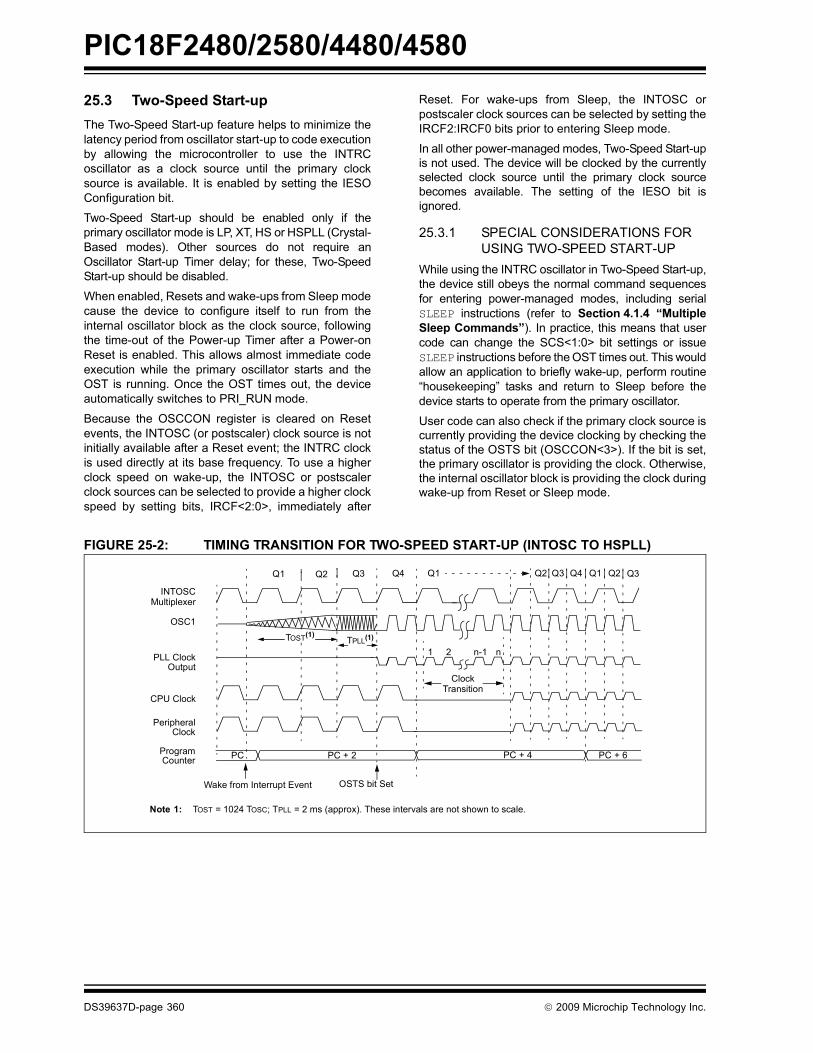
PIC18F2480/2580/4480/4580
25.3 Two-Speed Start-upThe Two-Speed Start-up feature helps to minimize thelatency period from oscillator start-up to code executionby allowing the microcontroller to use the INTRCoscillator as a clock source until the primary clocksource is available. It is enabled by setting the IESOConfiguration bit.Two-Speed Start-up should be enabled only if theprimary oscillator mode is LP, XT, HS or HSPLL (Crystal-Based modes). Other sources do not require anOscillator Start-up Timer delay; for these, Two-SpeedStart-up should be disabled.
When enabled, Resets and wake-ups from Sleep modecause the device to configure itself to run from theinternal oscillator block as the clock source, followingthe time-out of the Power-up Timer after a Power-onReset is enabled. This allows almost immediate codeexecution while the primary oscillator starts and theOST is running. Once the OST times out, the deviceautomatically switches to PRI_RUN mode.
Because the OSCCON register is cleared on Resetevents, the INTOSC (or postscaler) clock source is notinitially available after a Reset event; the INTRC clockis used directly at its base frequency. To use a higherclock speed on wake-up, the INTOSC or postscalerclock sources can be selected to provide a higher clockspeed by setting bits, IRCF<2:0>, immediately after
Reset. For wake-ups from Sleep, the INTOSC orpostscaler clock sources can be selected by setting theIRCF2:IRCF0 bits prior to entering Sleep mode.
In all other power-managed modes, Two-Speed Start-upis not used. The device will be clocked by the currentlyselected clock source until the primary clock sourcebecomes available. The setting of the IESO bit isignored.
25.3.1 SPECIAL CONSIDERATIONS FOR USING TWO-SPEED START-UP
While using the INTRC oscillator in Two-Speed Start-up,the device still obeys the normal command sequencesfor entering power-managed modes, including serialSLEEP instructions (refer to Section 4.1.4 “MultipleSleep Commands”). In practice, this means that usercode can change the SCS<1:0> bit settings or issueSLEEP instructions before the OST times out. This wouldallow an application to briefly wake-up, perform routine“housekeeping” tasks and return to Sleep before thedevice starts to operate from the primary oscillator.
User code can also check if the primary clock source iscurrently providing the device clocking by checking thestatus of the OSTS bit (OSCCON<3>). If the bit is set,the primary oscillator is providing the clock. Otherwise,the internal oscillator block is providing the clock duringwake-up from Reset or Sleep mode.
FIGURE 25-2: TIMING TRANSITION FOR TWO-SPEED START-UP (INTOSC TO HSPLL)
Q1 Q3 Q4
OSC1
Peripheral
Program PC PC + 2
INTOSC
PLL Clock
Q1
PC + 6
Q2
Output
Q3 Q4 Q1
CPU Clock
PC + 4
Clock
Counter
Q2 Q2 Q3
Note 1: TOST = 1024 TOSC; TPLL = 2 ms (approx). These intervals are not shown to scale.
Wake from Interrupt Event
TPLL(1)
1 2 n-1 n
Clock
OSTS bit Set
Transition
Multiplexer
TOST(1)
DS39637D-page 360 © 2009 Microchip Technology Inc.

PIC18F2480/2580/4480/4580
25.4 Fail-Safe Clock MonitorThe Fail-Safe Clock Monitor (FSCM) allows themicrocontroller to continue operation in the event of anexternal oscillator failure by automatically switching thedevice clock to the internal oscillator block. The FSCMfunction is enabled by setting the FCMEN Configurationbit.When FSCM is enabled, the INTRC oscillator runs atall times to monitor clocks to peripherals and provide abackup clock in the event of a clock failure. Clockmonitoring (shown in Figure 25-3) is accomplished bycreating a sample clock signal, which is the INTRC out-put divided by 64. This allows ample time betweenFSCM sample clocks for a peripheral clock edge tooccur. The peripheral device clock and the sampleclock are presented as inputs to the Clock Monitor(CM) latch. The CM is set on the falling edge of thedevice clock source, but cleared on the rising edge ofthe sample clock.
FIGURE 25-3: FSCM BLOCK DIAGRAM
Clock failure is tested for on the falling edge of thesample clock. If a sample clock falling edge occurswhile CM is still set, a clock failure has been detected(Figure 25-4). This causes the following:
• the FSCM generates an oscillator fail interrupt by setting bit, OSCFIF (PIR2<7>);
• the device clock source is switched to the internal oscillator block (OSCCON is not updated to show the current clock source – this is the Fail-Safe condition); and
• the WDT is reset.
During switchover, the postscaler frequency from theinternal oscillator block may not be sufficiently stable fortiming-sensitive applications. In these cases, it may bedesirable to select another clock configuration and enteran alternate power-managed mode. This can be done toattempt a partial recovery or execute a controlled shut-down. See Section 4.1.4 “Multiple Sleep Commands”and Section 25.3.1 “Special Considerations forUsing Two-Speed Start-up” for more details.
To use a higher clock speed on wake-up, the INTOSCor postscaler clock sources can be selected to providea higher clock speed by setting bits, IRCF<2:0>,immediately after Reset. For wake-ups from Sleep, theINTOSC or postscaler clock sources can be selectedby setting the IRCF<2:0> bits prior to entering Sleepmode.
The FSCM will detect failures of the primary or second-ary clock sources only. If the internal oscillator blockfails, no failure would be detected, nor would any actionbe possible.
25.4.1 FSCM AND THE WATCHDOG TIMERBoth the FSCM and the WDT are clocked by theINTRC oscillator. Since the WDT operates with aseparate divider and counter, disabling the WDT hasno effect on the operation of the INTRC oscillator whenthe FSCM is enabled.
As already noted, the clock source is switched to theINTOSC clock when a clock failure is detected.Depending on the frequency selected by theIRCF<2:0> bits, this may mean a substantial change inthe speed of code execution. If the WDT is enabledwith a small prescale value, a decrease in clock speedallows a WDT time-out to occur and a subsequentdevice Reset. For this reason, Fail-Safe Clock eventsalso reset the WDT and postscaler, allowing it to starttiming from when execution speed was changed anddecreasing the likelihood of an erroneous time-out.
25.4.2 EXITING FAIL-SAFE OPERATIONThe Fail-Safe condition is terminated by either a deviceReset or by entering a power-managed mode. OnReset, the controller starts the primary clock sourcespecified in Configuration Register 1H (with anyrequired start-up delays that are required for theoscillator mode, such as OST or PLL timer). TheINTOSC multiplexer provides the device clock until theprimary clock source becomes ready (similar to a Two-Speed Start-up). The clock source is then switched tothe primary clock (indicated by the OSTS bit in theOSCCON register becoming set). The Fail-Safe ClockMonitor then resumes monitoring the peripheral clock.
The primary clock source may never become readyduring start-up. In this case, operation is clocked by theINTOSC multiplexer. The OSCCON register will remainin its Reset state until a power-managed mode isentered.
Peripheral
INTRC÷ 64
S
C
Q
(32 μs) 488 Hz(2.048 ms)
Clock MonitorLatch (CM)
(edge-triggered)
ClockFailure
Detected
Source
Clock
Q
© 2009 Microchip Technology Inc. DS39637D-page 361
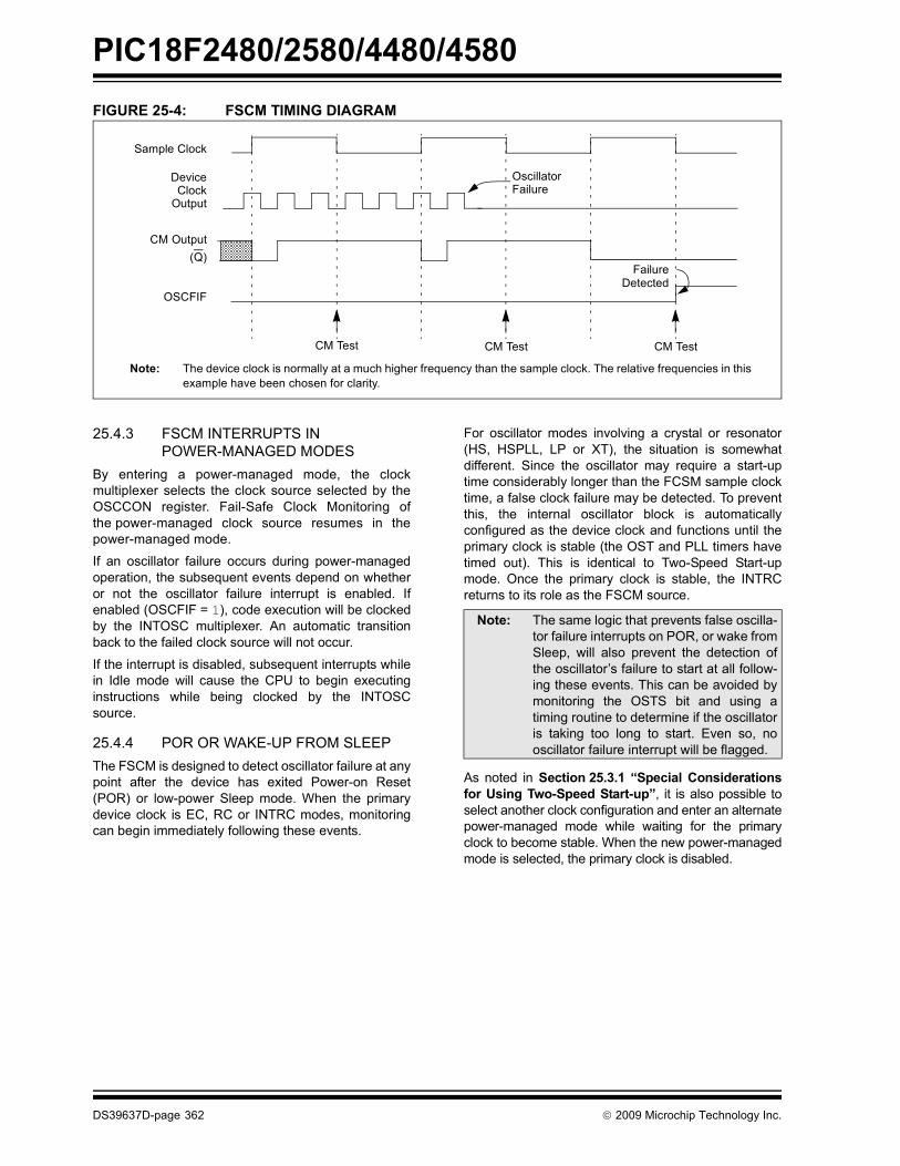
PIC18F2480/2580/4480/4580
FIGURE 25-4: FSCM TIMING DIAGRAM25.4.3 FSCM INTERRUPTS IN POWER-MANAGED MODES
By entering a power-managed mode, the clockmultiplexer selects the clock source selected by theOSCCON register. Fail-Safe Clock Monitoring ofthe power-managed clock source resumes in thepower-managed mode.
If an oscillator failure occurs during power-managedoperation, the subsequent events depend on whetheror not the oscillator failure interrupt is enabled. Ifenabled (OSCFIF = 1), code execution will be clockedby the INTOSC multiplexer. An automatic transitionback to the failed clock source will not occur.
If the interrupt is disabled, subsequent interrupts whilein Idle mode will cause the CPU to begin executinginstructions while being clocked by the INTOSCsource.
25.4.4 POR OR WAKE-UP FROM SLEEPThe FSCM is designed to detect oscillator failure at anypoint after the device has exited Power-on Reset(POR) or low-power Sleep mode. When the primarydevice clock is EC, RC or INTRC modes, monitoringcan begin immediately following these events.
For oscillator modes involving a crystal or resonator(HS, HSPLL, LP or XT), the situation is somewhatdifferent. Since the oscillator may require a start-uptime considerably longer than the FCSM sample clocktime, a false clock failure may be detected. To preventthis, the internal oscillator block is automaticallyconfigured as the device clock and functions until theprimary clock is stable (the OST and PLL timers havetimed out). This is identical to Two-Speed Start-upmode. Once the primary clock is stable, the INTRCreturns to its role as the FSCM source.
As noted in Section 25.3.1 “Special Considerationsfor Using Two-Speed Start-up”, it is also possible toselect another clock configuration and enter an alternatepower-managed mode while waiting for the primaryclock to become stable. When the new power-managedmode is selected, the primary clock is disabled.
OSCFIF
CM Output
DeviceClock
Output
Sample Clock
FailureDetected
OscillatorFailure
Note: The device clock is normally at a much higher frequency than the sample clock. The relative frequencies in thisexample have been chosen for clarity.
(Q)
CM Test CM Test CM Test
Note: The same logic that prevents false oscilla-tor failure interrupts on POR, or wake fromSleep, will also prevent the detection ofthe oscillator’s failure to start at all follow-ing these events. This can be avoided bymonitoring the OSTS bit and using atiming routine to determine if the oscillatoris taking too long to start. Even so, nooscillator failure interrupt will be flagged.
DS39637D-page 362 © 2009 Microchip Technology Inc.

PIC18F2480/2580/4480/4580
25.5 Program Verification andCode ProtectionThe overall structure of the code protection on thePIC18 Flash devices differs significantly from otherPIC® devices.
The user program memory is divided into five blocks.One of these is a boot block of 2 Kbytes. The remainderof the memory is divided into four blocks on binaryboundaries.
Each of the five blocks has three code protection bitsassociated with them. They are:
• Code-Protect bit (CPn)• Write-Protect bit (WRTn)• External Block Table Read bit (EBTRn)
Figure 25-5 shows the program memory organizationfor 16 and 32-Kbyte devices and the specific codeprotection bit associated with each block. The actuallocations of the bits are summarized in Table 25-3.
FIGURE 25-5: CODE-PROTECTED PROGRAM MEMORY FOR PIC18F2480/2580/4480/4580
AddressRange
MEMORY SIZE/DEVICE
32 Kbytes(PIC18F2580/4580)
16 Kbytes(PIC18F2480/4480)
Block Code ProtectionControlled by:
BBSIZ 0 1 0 1
000000h Boot Block 1 kW Boot Block
2 kW
Boot Block 1 kW Boot Block
2 kWCPB, WRTB, EBRTB
(Boot Block)0007FFh
000800h
Block 0 3 kW
Block 03 kW
000FFFh
001000h Block 02 kW
Block 02 kW
CP0, WRT0, EBRT0(Block 0)001FFFh
002000h
Block 14 kW
Block 14 kW
Block 14 kW
Block 14 kW
CP!, WRT1, EBRT1(Block 1)
003FFFh
004000h
Block 24 kW
Block 24 kW
UnimplementedRead ‘0’s
UnimplementedRead ‘0’s
CP2, WRT2, EBRT2(Block 2)
005FFFh
006000h
Block 34 kW
Block 34 kW
CP3, WRT3, EBTR3(Block 3)
007FFFh
008000h
UnimplementedRead ‘0’s
UnimplementedRead ‘0’s (Unimplemented Memory Space)
1FFFFFh
© 2009 Microchip Technology Inc. DS39637D-page 363

PIC18F2480/2580/4480/4580
TABLE 25-3: SUMMARY OF CODE PROTECTION REGISTERS25.5.1 PROGRAM MEMORYCODE PROTECTION
The program memory may be read to or written fromany location using the table read and table writeinstructions. The Device ID may be read with tablereads. The Configuration registers may be read andwritten with the table read and table write instructions.
In normal execution mode, the CPn bits have no directeffect. CPn bits inhibit external reads and writes. Ablock of user memory may be protected from tablewrites if the WRTn Configuration bit is ‘0’. The EBTRnbits control table reads. For a block of user memorywith the EBTRn bit set to ‘0’, a table read instructionthat executes from within that block is allowed to read.
A table read instruction that executes from a locationoutside of that block is not allowed to read and willresult in reading ‘0’s. Figures 25-6 through 25-8illustrate table write and table read protection.
FIGURE 25-6: TABLE WRITE (WRTn) DISALLOWED
File Name Bit 7 Bit 6 Bit 5 Bit 4 Bit 3 Bit 2 Bit 1 Bit 0
300008h CONFIG5L — — — — CP3* CP2 CP1 CP0300009h CONFIG5H CPD CPB — — — — — —30000Ah CONFIG6L — — — — WRT3* WRT2 WRT1 WRT030000Bh CONFIG6H WRTD WRTB WRTC — — — — —30000Ch CONFIG7L — — — — EBTR3* EBTR2 EBTR1 EBTR030000Dh CONFIG7H — EBTRB — — — — — —Legend: Shaded cells are unimplemented.
* Unimplemented in PIC18FX480 devices; maintain this bit set.
Note: Code protection bits may only be written toa ‘0’ from a ‘1’ state. It is not possible towrite a ‘1’ to a bit in the ‘0’ state. Codeprotection bits are only set to ‘1’ by a fullchip erase or block erase function. The fullchip erase and block erase functions canonly be initiated via ICSP or an externalprogrammer.
000000h
0007FFh000800h
003FFFh004000h
007FFFh008000h
00BFFFh00C000h
00FFFFh
WRTB, EBTRB = 11
WRT0, EBTR0 = 01
WRT1, EBTR1 = 11
WRT2, EBTR2 = 11
WRT3, EBTR3 = 11
TBLWT*
TBLPTR = 0008FFh
PC = 003FFEh
TBLWT*PC = 00BFFEh
Register Values Program Memory Configuration Bit Settings
Results: All table writes disabled to Blockn whenever WRTn = 0.
DS39637D-page 364 © 2009 Microchip Technology Inc.

PIC18F2480/2580/4480/4580
FIGURE 25-7: EXTERNAL BLOCK TABLE READ (EBTRn) DISALLOWEDFIGURE 25-8: EXTERNAL BLOCK TABLE READ (EBTRn) ALLOWED
WRTB, EBTRB = 11
WRT0, EBTR0 = 10
WRT1, EBTR1 = 11
WRT2, EBTR2 = 11
WRT3, EBTR3 = 11
TBLRD*
TBLPTR = 0008FFh
PC = 007FFEh
Results: All table reads from external blocks to Blockn are disabled whenever EBTRn = 0. TABLAT register returns a value of ‘0’.
Register Values Program Memory Configuration Bit Settings
000000h
0007FFh000800h
003FFFh004000h
007FFFh008000h
00BFFFh00C000h
00FFFFh
WRTB, EBTRB = 11
WRT0, EBTR0 = 10
WRT1, EBTR1 = 11
WRT2, EBTR2 = 11
WRT3, EBTR3 = 11
TBLRD*
TBLPTR = 0008FFh
PC = 003FFEh
Register Values Program Memory Configuration Bit Settings
Results: Table reads permitted within Blockn, even when EBTRBn = 0.TABLAT register returns the value of the data at the location TBLPTR.
000000h
0007FFh000800h
003FFFh004000h
007FFFh008000h
00BFFFh00C000h
00FFFFh
© 2009 Microchip Technology Inc. DS39637D-page 365

PIC18F2480/2580/4480/4580
25.5.2 DATA EEPROMCODE PROTECTIONThe entire data EEPROM is protected from externalreads and writes by two bits: CPD and WRTD. CPDinhibits external reads and writes of data EEPROM.WRTD inhibits internal and external writes to dataEEPROM. The CPU can continue to read and writedata EEPROM regardless of the protection bit settings.
25.5.3 CONFIGURATION REGISTER PROTECTION
The Configuration registers can be write-protected.The WRTC bit controls protection of the Configurationregisters. In normal execution mode, the WRTC bit isreadable only. WRTC can only be written via ICSP oran external programmer.
25.6 ID LocationsEight memory locations (200000h-200007h) aredesignated as ID locations, where the user can storechecksum or other code identification numbers. Theselocations are both readable and writable during normalexecution through the TBLRD and TBLWT instructionsor during program/verify. The ID locations can be readwhen the device is code-protected.
25.7 In-Circuit Serial ProgrammingPIC18F2480/2580/4480/4580 microcontrollers can beserially programmed while in the end application circuit.This is simply done with two lines for clock and dataand three other lines for power, ground and theprogramming voltage. This allows customers to manu-facture boards with unprogrammed devices and thenprogram the microcontroller just before shipping theproduct. This also allows the most recent firmware or acustom firmware to be programmed.
25.8 In-Circuit DebuggerWhen the DEBUG Configuration bit is programmed toa ‘0’, the In-Circuit Debugger functionality is enabled.This function allows simple debugging functions whenused with MPLAB® IDE. When the microcontroller hasthis feature enabled, some resources are not availablefor general use. Table 25-4 shows which resources arerequired by the background debugger.
TABLE 25-4: DEBUGGER RESOURCES
To use the In-Circuit Debugger function of the micro-controller, the design must implement In-Circuit SerialProgramming connections to MCLR/VPP/RE3, VDD,VSS, RB7 and RB6. This will interface to the In-Circuitdebugger module available from Microchip or one ofthe third party development tool companies.
25.9 Single-Supply ICSP ProgrammingThe LVP Configuration bit enables Single-Supply ICSPProgramming (formerly known as Low-Voltage ICSPProgramming or LVP). When Single-Supply Program-ming is enabled, the microcontroller can beprogrammed without requiring high voltage beingapplied to the MCLR/VPP/RE3 pin, but the RB5/KBI1/PGM pin is then dedicated to controlling Program modeentry and is not available as a general purpose I/O pin.
While programming using Single-Supply Program-ming, VDD is applied to the MCLR/VPP/RE3 pin as innormal execution mode. To enter Programming mode,VDD is applied to the PGM pin.
If Single-Supply ICSP Programming mode will not beused, the LVP bit can be cleared. RB5/KBI1/PGM thenbecomes available as the digital I/O pin, RB5. The LVPbit may be set or cleared only when using standardhigh-voltage programming (VIHH applied to the MCLR/VPP/RE3 pin). Once LVP has been disabled, only thestandard high-voltage programming is available andmust be used to program the device.
Memory that is not code-protected can be erased usingeither a block erase, or erased row by row, then writtenat any specified VDD. If code-protected memory is to beerased, a block erase is required. If a block erase is tobe performed when using Low-Voltage Programming,the device must be supplied with VDD of 4.5V to 5.5V.
I/O pins: RB6, RB7Stack: 2 levels
Note: Memory resources listed in MPLAB® IDE.
Note 1: High-voltage programming is always avail-able, regardless of the state of the LVP bit,by applying VIHH to the MCLR pin.
2: While in Low-Voltage ICSP Programmingmode, the RB5 pin can no longer be usedas a general purpose I/O pin and shouldbe held low during normal operation.
3: When using Low-Voltage ICSP Program-ming (LVP) and the pull-ups on PORTBare enabled, bit 5 in the TRISB registermust be cleared to disable the pull-up onRB5 and ensure the proper operation ofthe device.
4: If the device Master Clear is disabled,verify that either of the following is done toensure proper entry into ICSP mode:
a) disable Low-Voltage Programming(CONFIG4l<2> = 0); or
b) make certain that RB5/PGM is heldlow during entry into ICSP.
DS39637D-page 366 © 2009 Microchip Technology Inc.

PIC18F2480/2580/4480/4580
26.0 INSTRUCTION SET SUMMARYPIC18F2480/2580/4480/4580 devices incorporate thestandard set of 75 PIC18 core instructions, as well asan extended set of 8 new instructions for the optimiza-tion of code that is recursive or that utilizes a softwarestack. The extended set is discussed later in thissection.
26.1 Standard Instruction SetThe standard PIC18 instruction set adds manyenhancements to the previous PIC® MCU instructionsets, while maintaining an easy migration from thesePIC MCU instruction sets. Most instructions are asingle program memory word (16 bits), but there arefour instructions that require two program memorylocations.
Each single-word instruction is a 16-bit word dividedinto an opcode, which specifies the instruction type andone or more operands, which further specify theoperation of the instruction.
The instruction set is highly orthogonal and is groupedinto four basic categories:
• Byte-oriented operations• Bit-oriented operations• Literal operations• Control operations
The PIC18 instruction set summary in Table 26-2 listsbyte-oriented, bit-oriented, literal and controloperations. Table 26-1 shows the opcode fielddescriptions.
Most byte-oriented instructions have three operands:
1. The file register (specified by ‘f’) 2. The destination of the result (specified by ‘d’) 3. The accessed memory (specified by ‘a’)
The file register designator, ‘f’, specifies which fileregister is to be used by the instruction. The destinationdesignator, ‘d’, specifies where the result of the opera-tion is to be placed. If ‘d’ is ‘0’, the result is placed in theWREG register. If ‘d’ is ‘1’, the result is placed in the fileregister specified in the instruction.
All bit-oriented instructions have three operands:
1. The file register (specified by ‘f’) 2. The bit in the file register (specified by ‘b’) 3. The accessed memory (specified by ‘a’)
The bit field designator, ‘b’, selects the number of the bitaffected by the operation, while the file register desig-nator, ‘f’, represents the number of the file in which thebit is located.
The literal instructions may use some of the followingoperands:
• A literal value to be loaded into a file register (specified by ‘k’)
• The desired FSR register to load the literal value into (specified by ‘f’)
• No operand required (specified by ‘—’)
The control instructions may use some of the followingoperands:
• A program memory address (specified by ‘n’)• The mode of the CALL or RETURN instructions
(specified by ‘s’)• The mode of the table read and table write
instructions (specified by ‘m’)• No operand required
(specified by ‘—’)
All instructions are a single word, except for fourdouble-word instructions. These instructions weremade double-word to contain the required informationin 32 bits. In the second word, the 4 MSbs are ‘1’s. Ifthis second word is executed as an instruction (byitself), it will execute as a NOP.
All single-word instructions are executed in a singleinstruction cycle, unless a conditional test is true or theprogram counter is changed as a result of the instruc-tion. In these cases, the execution takes two instructioncycles with the additional instruction cycle(s) executedas a NOP.
The double-word instructions execute in two instructioncycles.
One instruction cycle consists of four oscillator periods.Thus, for an oscillator frequency of 4 MHz, the normalinstruction execution time is 1 μs. If a conditional test istrue, or the program counter is changed as a result ofan instruction, the instruction execution time is 2 μs.Two-word branch instructions (if true) would take 3 μs.
Figure 26-1 shows the general formats that the instruc-tions can have. All examples use the convention ‘nnh’to represent a hexadecimal number.
The instruction set summary, shown in Table 26-2, liststhe standard instructions recognized by the MicrochipMPASM Assembler.
Section 26.1.1 “Standard Instruction Set” providesa description of each instruction.
© 2009 Microchip Technology Inc. DS39637D-page 367

PIC18F2480/2580/4480/4580
TABLE 26-1: OPCODE FIELD DESCRIPTIONSField Descriptiona RAM access bit
a = 0: RAM location in Access RAM (BSR register is ignored)a = 1: RAM bank is specified by BSR register
bbb Bit address within an 8-bit file register (0 to 7).BSR Bank Select Register. Used to select the current RAM bank.C, DC, Z, OV, N ALU Status bits: Carry, Digit Carry, Zero, Overflow, Negative.d Destination select bit
d = 0: store result in WREGd = 1: store result in file register f
dest Destination: either the WREG register or the specified register file location.f 8-bit Register file address (00h to FFh), or 2-bit FSR designator (0h to 3h).fs 12-bit Register file address (000h to FFFh). This is the source address. fd 12-bit Register file address (000h to FFFh). This is the destination address. GIE Global Interrupt Enable bit.k Literal field, constant data or label (may be either an 8-bit, 12-bit or a 20-bit value)label Label namemm The mode of the TBLPTR register for the table read and table write instructions.
Only used with table read and table write instructions:* No change to register (such as TBLPTR with table reads and writes)*+ Post-Increment register (such as TBLPTR with table reads and writes)*- Post-Decrement register (such as TBLPTR with table reads and writes)+* Pre-Increment register (such as TBLPTR with table reads and writes)n The relative address (2’s complement number) for relative branch instructions or the direct address for
Call/Branch and Return instructionsPC Program Counter.PCL Program Counter Low Byte.PCH Program Counter High Byte.PCLATH Program Counter High Byte Latch.PCLATU Program Counter Upper Byte Latch.PD Power-down bit.PRODH Product of Multiply High Byte.PRODL Product of Multiply Low Byte.s Fast Call/Return mode select bit
s = 0: do not update into/from shadow registerss = 1: certain registers loaded into/from shadow registers (Fast mode)
TBLPTR 21-bit Table Pointer (points to a program memory location).TABLAT 8-bit Table Latch.TO Time-out bit.TOS Top-of-Stack.u Unused or unchanged.WDT Watchdog Timer.WREG Working register (accumulator).x Don’t care (‘0’ or ‘1’). The assembler will generate code with x = 0. It is the recommended form of use for
compatibility with all Microchip software tools.zs 7-bit offset value for indirect addressing of register files (source).zd 7-bit offset value for indirect addressing of register files (destination). Optional argument.[text] Indicates an indexed address.(text) The contents of text.[expr]<n> Specifies bit n of the register indicated by the pointer expr.→ Assigned to.< > Register bit field.∈ In the set of.italics User-defined term (font is Courier New).
DS39637D-page 368 © 2009 Microchip Technology Inc.

PIC18F2480/2580/4480/4580
FIGURE 26-1: GENERAL FORMAT FOR INSTRUCTIONSByte-oriented file register operations
15 10 9 8 7 0
d = 0 for result destination to be WREG register
OPCODE d a f (FILE #)
d = 1 for result destination to be file register (f)a = 0 to force Access Bank
Bit-oriented file register operations
15 12 11 9 8 7 0OPCODE b (BIT #) a f (FILE #)
b = 3-bit position of bit in file register (f)
Literal operations
15 8 7 0 OPCODE k (literal)
k = 8-bit immediate value
Byte to Byte move operations (2-word)
15 12 11 0OPCODE f (Source FILE #)
CALL, GOTO and Branch operations 15 8 7 0
OPCODE n<7:0> (literal)
n = 20-bit immediate value
a = 1 for BSR to select bankf = 8-bit file register address
a = 0 to force Access Banka = 1 for BSR to select bankf = 8-bit file register address
15 12 11 01111 n<19:8> (literal)
15 12 11 0 1111 f (Destination FILE #)
f = 12-bit file register address
Control operations
Example Instruction
ADDWF MYREG, W, B
MOVFF MYREG1, MYREG2
BSF MYREG, bit, B
MOVLW 7Fh
GOTO Label
15 8 7 0
OPCODE n<7:0> (literal)
15 12 11 0
1111 n<19:8> (literal)
CALL MYFUNC
15 11 10 0
OPCODE n<10:0> (literal)
S = Fast bit
BRA MYFUNC
15 8 7 0
OPCODE n<7:0> (literal) BC MYFUNC
S
© 2009 Microchip Technology Inc. DS39637D-page 369
PIC18F2480/2580/4480/4580
44
4
t
ll
TABLE 26-2: PIC18FXXXX INSTRUCTION SET
Mnemonic,Operands Description Cycles
16-Bit Instruction Word StatusAffected Notes
MSb LSb
BYTE-ORIENTED OPERATIONSADDWFADDWFCANDWFCLRFCOMFCPFSEQCPFSGTCPFSLTDECFDECFSZDCFSNZINCFINCFSZINFSNZIORWFMOVFMOVFF
MOVWFMULWFNEGFRLCFRLNCFRRCFRRNCFSETFSUBFWB
SUBWFSUBWFB
SWAPFTSTFSZXORWF
f, d, af, d, af, d, af, af, d, af, af, af, af, d, af, d, af, d, af, d, af, d, af, d, af, d, af, d, afs, fd
f, af, af, af, d, af, d, af, d, af, d, af, af, d, a
f, d, af, d, a
f, d, af, af, d, a
Add WREG and fAdd WREG and Carry bit to fAND WREG with fClear fComplement fCompare f with WREG, Skip =Compare f with WREG, Skip >Compare f with WREG, Skip <Decrement fDecrement f, Skip if 0Decrement f, Skip if Not 0Increment fIncrement f, Skip if 0Increment f, Skip if Not 0Inclusive OR WREG with fMove fMove fs (source) to 1st word
fd (destination) 2nd wordMove WREG to fMultiply WREG with fNegate fRotate Left f through CarryRotate Left f (No Carry)Rotate Right f through CarryRotate Right f (No Carry)Set fSubtract f from WREG with Borrow Subtract WREG from fSubtract WREG from f with BorrowSwap Nibbles in fTest f, Skip if 0Exclusive OR WREG with f
111111 (2 or 3)1 (2 or 3)1 (2 or 3)11 (2 or 3)1 (2 or 3)11 (2 or 3)1 (2 or 3)112
111111111
11
11 (2 or 3)1
001000100001011000010110011001100000001001000010001101000001010111001111011000000110001101000011010001100101
01010101
001101100001
01da00da01da101a11da001a010a000a01da11da11da10da11da10da00da00daffffffff111a001a110a01da01da00da00da100a01da
11da10da
10da011a10da
ffffffffffffffffffffffffffffffffffffffffffffffffffffffffffffffffffffffffffffffffffffffffffffffffffffffffffff
ffffffff
ffffffffffff
ffffffffffffffffffffffffffffffffffffffffffffffffffffffffffffffffffffffffffffffffffffffffffffffffffffffffffff
ffffffff
ffffffffffff
C, DC, Z, OV, NC, DC, Z, OV, NZ, NZZ, NNoneNoneNoneC, DC, Z, OV, NNoneNoneC, DC, Z, OV, NNoneNoneZ, NZ, NNone
NoneNoneC, DC, Z, OV, NC, Z, NZ, NC, Z, NZ, NNoneC, DC, Z, OV, N
C, DC, Z, OV, NC, DC, Z, OV, N
NoneNoneZ, N
1, 21, 21,221, 2441, 21, 2, 3, 1, 2, 3, 1, 21, 2, 3, 41, 21, 21
1, 2
1, 2
1, 2
1, 2
41, 2
Note 1: When a PORT register is modified as a function of itself (e.g., MOVF PORTB, 1, 0), the value used will be thavalue present on the pins themselves. For example, if the data latch is ‘1’ for a pin configured as input and is driven low by an external device, the data will be written back with a ‘0’.
2: If this instruction is executed on the TMR0 register (and where applicable, ‘d’ = 1), the prescaler will be clearedif assigned.
3: If the Program Counter (PC) is modified or a conditional test is true, the instruction requires two cycles. The second cycle is executed as a NOP.
4: Some instructions are two-word instructions. The second word of these instructions will be executed as a NOPunless the first word of the instruction retrieves the information embedded in these 16 bits. This ensures that aprogram memory locations have a valid instruction.
5: If the table write starts the write cycle to internal memory, the write will continue until terminated.
DS39637D-page 370 © 2009 Microchip Technology Inc.

PIC18F2480/2580/4480/4580
t
ll
BIT-ORIENTED OPERATIONSBCFBSFBTFSCBTFSSBTG
f, b, af, b, af, b, af, b, af, b, a
Bit Clear fBit Set fBit Test f, Skip if ClearBit Test f, Skip if SetBit Toggle f
111 (2 or 3)1 (2 or 3)1
10011000101110100111
bbbabbbabbbabbbabbba
ffffffffffffffffffff
ffffffffffffffffffff
NoneNoneNoneNoneNone
1, 21, 23, 43, 41, 2
CONTROL OPERATIONSBCBNBNCBNNBNOVBNZBOVBRABZCALL
CLRWDTDAWGOTO
NOPNOPPOPPUSHRCALLRESETRETFIE
RETLWRETURNSLEEP
nnnnnnnnnn, s
——n
————n
s
ks—
Branch if CarryBranch if NegativeBranch if Not CarryBranch if Not NegativeBranch if Not OverflowBranch if Not ZeroBranch if OverflowBranch Unconditionally Branch if ZeroCall Subroutine 1st word
2nd wordClear Watchdog TimerDecimal Adjust WREGGo to Address 1st word
2nd wordNo OperationNo OperationPop Top of Return Stack (TOS)Push Top of Return Stack (TOS)Relative CallSoftware Device ResetReturn from Interrupt Enable
Return with Literal in WREG Return from SubroutineGo into Standby mode
1 (2)1 (2)1 (2)1 (2)1 (2)1 (2)1 (2)21 (2)2
112
1111212
221
1110111011101110111011101110110111101110111100000000111011110000111100000000110100000000
000000000000
00100110001101110101000101000nnn0000110skkkk000000001111kkkk0000xxxx000000001nnn00000000
110000000000
nnnnnnnnnnnnnnnnnnnnnnnnnnnnnnnnnnnnkkkkkkkk00000000kkkkkkkk0000xxxx00000000nnnn11110001
kkkk00010000
nnnnnnnnnnnnnnnnnnnnnnnnnnnnnnnnnnnnkkkkkkkk01000111kkkkkkkk0000xxxx01100101nnnn1111000s
kkkk001s0011
NoneNoneNoneNoneNoneNoneNoneNoneNoneNone
TO, PDCNone
NoneNoneNoneNoneNoneAllGIE/GIEH, PEIE/GIELNoneNoneTO, PD
4
TABLE 26-2: PIC18FXXXX INSTRUCTION SET (CONTINUED)
Mnemonic,Operands Description Cycles
16-Bit Instruction Word StatusAffected Notes
MSb LSb
Note 1: When a PORT register is modified as a function of itself (e.g., MOVF PORTB, 1, 0), the value used will be thavalue present on the pins themselves. For example, if the data latch is ‘1’ for a pin configured as input and is driven low by an external device, the data will be written back with a ‘0’.
2: If this instruction is executed on the TMR0 register (and where applicable, ‘d’ = 1), the prescaler will be clearedif assigned.
3: If the Program Counter (PC) is modified or a conditional test is true, the instruction requires two cycles. The second cycle is executed as a NOP.
4: Some instructions are two-word instructions. The second word of these instructions will be executed as a NOPunless the first word of the instruction retrieves the information embedded in these 16 bits. This ensures that aprogram memory locations have a valid instruction.
5: If the table write starts the write cycle to internal memory, the write will continue until terminated.
© 2009 Microchip Technology Inc. DS39637D-page 371

PIC18F2480/2580/4480/4580
t
ll
LITERAL OPERATIONSADDLWANDLWIORLWLFSR
MOVLBMOVLWMULLWRETLWSUBLWXORLW
kkkf, k
kkkkkk
Add Literal and WREGAND Literal with WREGInclusive OR Literal with WREGMove literal (12-bit) 2nd word to FSR(f) 1st wordMove Literal to BSR<3:0>Move Literal to WREGMultiply Literal with WREGReturn with Literal in WREG Subtract WREG from LiteralExclusive OR Literal with WREG
1112
111211
00000000000011101111000000000000000000000000
11111011100111100000000111101101110010001010
kkkkkkkkkkkk00ffkkkk0000kkkkkkkkkkkkkkkkkkkk
kkkkkkkkkkkkkkkkkkkkkkkkkkkkkkkkkkkkkkkkkkkk
C, DC, Z, OV, NZ, NZ, NNone
NoneNoneNoneNoneC, DC, Z, OV, NZ, N
DATA MEMORY ↔ PROGRAM MEMORY OPERATIONSTBLRD*TBLRD*+TBLRD*-TBLRD+*TBLWT*TBLWT*+TBLWT*-TBLWT+*
Table ReadTable Read with Post-IncrementTable Read with Post-DecrementTable Read with Pre-IncrementTable WriteTable Write with Post-IncrementTable Write with Post-DecrementTable Write with Pre-Increment
2
2
00000000000000000000000000000000
00000000000000000000000000000000
00000000000000000000000000000000
10001001101010111100110111101111
NoneNoneNoneNoneNoneNoneNoneNone
5555
TABLE 26-2: PIC18FXXXX INSTRUCTION SET (CONTINUED)
Mnemonic,Operands Description Cycles
16-Bit Instruction Word StatusAffected Notes
MSb LSb
Note 1: When a PORT register is modified as a function of itself (e.g., MOVF PORTB, 1, 0), the value used will be thavalue present on the pins themselves. For example, if the data latch is ‘1’ for a pin configured as input and is driven low by an external device, the data will be written back with a ‘0’.
2: If this instruction is executed on the TMR0 register (and where applicable, ‘d’ = 1), the prescaler will be clearedif assigned.
3: If the Program Counter (PC) is modified or a conditional test is true, the instruction requires two cycles. The second cycle is executed as a NOP.
4: Some instructions are two-word instructions. The second word of these instructions will be executed as a NOPunless the first word of the instruction retrieves the information embedded in these 16 bits. This ensures that aprogram memory locations have a valid instruction.
5: If the table write starts the write cycle to internal memory, the write will continue until terminated.
DS39637D-page 372 © 2009 Microchip Technology Inc.

PIC18F2480/2580/4480/4580
26.1.1 STANDARD INSTRUCTION SETADDLW ADD Literal to W
Syntax: ADDLW k
Operands: 0 ≤ k ≤ 255
Operation: (W) + k → W
Status Affected: N, OV, C, DC, Z
Encoding: 0000 1111 kkkk kkkk
Description: The contents of W are added to the 8-bit literal ‘k’ and the result is placed in W.
Words: 1
Cycles: 1
Q Cycle Activity:Q1 Q2 Q3 Q4
Decode Readliteral ‘k’
Process Data
Write to W
Example: ADDLW 15h
Before InstructionW = 10h
After InstructionW = 25h
ADDWF ADD W to f
Syntax: ADDWF f ,d ,a
Operands: 0 ≤ f ≤ 255d ∈ [0,1]a ∈ [0,1]
Operation: (W) + (f) → dest
Status Affected: N, OV, C, DC, Z
Encoding: 0010 01da ffff ffff
Description: Add W to register ‘f’. If ‘d’ is ‘0’, the result is stored in W. If ‘d’ is ‘1’, the result is stored back in register ‘f’. If ‘a’ is ‘0’, the Access Bank is selected. If ‘a’ is ‘1’, the BSR is used to select the GPR bank. If ‘a’ is ‘0’ and the extended instruction set is enabled, this instruction operates in Indexed Literal Offset Addressing mode whenever f ≤ 95 (5Fh). See Section 26.2.3 “Byte-Oriented and Bit-Oriented Instructions in Indexed Literal Offset Mode” for details.
Words: 1
Cycles: 1
Q Cycle Activity:Q1 Q2 Q3 Q4
Decode Readregister ‘f’
Process Data
Write todestination
Example: ADDWF REG, 0, 0
Before InstructionW = 17hREG = 0C2h
After InstructionW = 0D9hREG = 0C2h
Note: All PIC18 instructions may take an optional label argument preceding the instruction mnemonic for use insymbolic addressing. If a label is used, the instruction format then becomes: label instruction argument(s).
© 2009 Microchip Technology Inc. DS39637D-page 373

PIC18F2480/2580/4480/4580
ADDWFC ADD W and Carry bit to f
Syntax: ADDWFC f ,d ,a
Operands: 0 ≤ f ≤ 255d ∈ [0,1]a ∈ [0,1]
Operation: (W) + (f) + (C) → dest
Status Affected: N,OV, C, DC, Z
Encoding: 0010 00da ffff ffff
Description: Add W, the Carry flag and data memory location ‘f’. If ‘d’ is ‘0’, the result is placed in W. If ‘d’ is ‘1’, the result is placed in data memory location ‘f’. If ‘a’ is ‘0’, the Access Bank is selected. If ‘a’ is ‘1’, the BSR is used to select the GPR bank. If ‘a’ is ‘0’ and the extended instruction set is enabled, this instruction operates in Indexed Literal Offset Addressing mode whenever f ≤ 95 (5Fh). See Section 26.2.3 “Byte-Oriented and Bit-Oriented Instructions in Indexed Literal Offset Mode” for details.
Words: 1
Cycles: 1
Q Cycle Activity:Q1 Q2 Q3 Q4
Decode Readregister ‘f’
Process Data
Write to destination
Example: ADDWFC REG, 0, 1
Before InstructionCarry bit = 1REG = 02hW = 4Dh
After InstructionCarry bit = 0REG = 02hW = 50h
ANDLW AND Literal with W
Syntax: ANDLW k
Operands: 0 ≤ k ≤ 255
Operation: (W) .AND. k → W
Status Affected: N, Z
Encoding: 0000 1011 kkkk kkkk
Description: The contents of W are ANDed with the 8-bit literal ‘k’. The result is placed in W.
Words: 1
Cycles: 1
Q Cycle Activity:Q1 Q2 Q3 Q4
Decode Read literal ‘k’
Process Data
Write to W
Example: ANDLW 05Fh
Before InstructionW = A3h
After InstructionW = 03h
DS39637D-page 374 © 2009 Microchip Technology Inc.

PIC18F2480/2580/4480/4580
ANDWF AND W with f
Syntax: ANDWF f ,d ,a
Operands: 0 ≤ f ≤ 255d ∈ [0,1]a ∈ [0,1]
Operation: (W) .AND. (f) → dest
Status Affected: N, Z
Encoding: 0001 01da ffff ffff
Description: The contents of W are AND’ed with register ‘f’. If ‘d’ is ‘0’, the result is stored in W. If ‘d’ is ‘1’, the result is stored back in register ‘f’. If ‘a’ is ‘0’, the Access Bank is selected. If ‘a’ is ‘1’, the BSR is used to select the GPR bank. If ‘a’ is ‘0’ and the extended instruction set is enabled, this instruction operates in Indexed Literal Offset Addressing mode whenever f ≤ 95 (5Fh). See Section 26.2.3 “Byte-Oriented and Bit-Oriented Instructions in Indexed Literal Offset Mode” for details.
Words: 1
Cycles: 1
Q Cycle Activity:Q1 Q2 Q3 Q4
Decode Readregister ‘f’
Process Data
Write to destination
Example: ANDWF REG, 0, 0
Before InstructionW = 17hREG = C2h
After InstructionW = 02hREG = C2h
BC Branch if Carry
Syntax: BC n
Operands: -128 ≤ n ≤ 127
Operation: if Carry bit is ‘1’,(PC) + 2 + 2n → PC
Status Affected: None
Encoding: 1110 0010 nnnn nnnn
Description: If the Carry bit is ‘1’, then the program will branch.The 2’s complement number ‘2n’ is added to the PC. Since the PC will have incremented to fetch the next instruction, the new address will be PC + 2 + 2n. This instruction is then a two-cycle instruction.
Words: 1
Cycles: 1(2)
Q Cycle Activity:If Jump:
Q1 Q2 Q3 Q4Decode Read literal
‘n’Process
DataWrite to PC
No operation
No operation
No operation
No operation
If No Jump:Q1 Q2 Q3 Q4
Decode Read literal ‘n’
Process Data
No operation
Example: HERE BC 5
Before InstructionPC = address (HERE)
After InstructionIf Carry = 1;
PC = address (HERE + 12)If Carry = 0;
PC = address (HERE + 2)
© 2009 Microchip Technology Inc. DS39637D-page 375

PIC18F2480/2580/4480/4580
BCF Bit Clear f
Syntax: BCF f, b ,a
Operands: 0 ≤ f ≤ 2550 ≤ b ≤ 7a ∈ [0,1]
Operation: 0 → f<b>
Status Affected: None
Encoding: 1001 bbba ffff ffff
Description: Bit ‘b’ in register ‘f’ is cleared.If ‘a’ is ‘0’, the Access Bank is selected. If ‘a’ is ‘1’, the BSR is used to select the GPR bank. If ‘a’ is ‘0’ and the extended instruction set is enabled, this instruction operates in Indexed Literal Offset Addressing mode whenever f ≤ 95 (5Fh). See Section 26.2.3 “Byte-Oriented and Bit-Oriented Instructions in Indexed Literal Offset Mode” for details.
Words: 1
Cycles: 1
Q Cycle Activity:Q1 Q2 Q3 Q4
Decode Readregister ‘f’
Process Data
Writeregister ‘f’
Example: BCF FLAG_REG, 7, 0
Before InstructionFLAG_REG = C7h
After InstructionFLAG_REG = 47h
BN Branch if Negative
Syntax: BN n
Operands: -128 ≤ n ≤ 127
Operation: if Negative bit is ‘1’,(PC) + 2 + 2n → PC
Status Affected: None
Encoding: 1110 0110 nnnn nnnn
Description: If the Negative bit is ‘1’, then the program will branch.The 2’s complement number ‘2n’ is added to the PC. Since the PC will have incremented to fetch the next instruction, the new address will be PC + 2 + 2n. This instruction is then a two-cycle instruction.
Words: 1
Cycles: 1(2)
Q Cycle Activity:If Jump:
Q1 Q2 Q3 Q4Decode Read literal
‘n’Process
DataWrite to PC
No operation
No operation
No operation
No operation
If No Jump:Q1 Q2 Q3 Q4
Decode Read literal ‘n’
Process Data
No operation
Example: HERE BN Jump
Before InstructionPC = address (HERE)
After InstructionIf Negative = 1;
PC = address (Jump)If Negative = 0;
PC = address (HERE + 2)
DS39637D-page 376 © 2009 Microchip Technology Inc.

PIC18F2480/2580/4480/4580
BNC Branch if Not Carry
Syntax: BNC n
Operands: -128 ≤ n ≤ 127
Operation: if Carry bit is ‘0’,(PC) + 2 + 2n → PC
Status Affected: None
Encoding: 1110 0011 nnnn nnnn
Description: If the Carry bit is ‘0’, then the program will branch.The 2’s complement number ‘2n’ is added to the PC. Since the PC will have incremented to fetch the next instruction, the new address will be PC + 2 + 2n. This instruction is then a two-cycle instruction.
Words: 1
Cycles: 1(2)
Q Cycle Activity:If Jump:
Q1 Q2 Q3 Q4Decode Read literal
‘n’Process
DataWrite to PC
No operation
No operation
No operation
No operation
If No Jump:Q1 Q2 Q3 Q4
Decode Read literal ‘n’
Process Data
No operation
Example: HERE BNC Jump
Before InstructionPC = address (HERE)
After InstructionIf Carry = 0;
PC = address (Jump)If Carry = 1;
PC = address (HERE + 2)
BNN Branch if Not Negative
Syntax: BNN n
Operands: -128 ≤ n ≤ 127
Operation: if Negative bit is ‘0’,(PC) + 2 + 2n → PC
Status Affected: None
Encoding: 1110 0111 nnnn nnnn
Description: If the Negative bit is ‘0’, then the program will branch.The 2’s complement number ‘2n’ is added to the PC. Since the PC will have incremented to fetch the next instruction, the new address will be PC + 2 + 2n. This instruction is then a two-cycle instruction.
Words: 1
Cycles: 1(2)
Q Cycle Activity:If Jump:
Q1 Q2 Q3 Q4Decode Read literal
‘n’Process
DataWrite to PC
No operation
No operation
No operation
No operation
If No Jump:Q1 Q2 Q3 Q4
Decode Read literal ‘n’
Process Data
No operation
Example: HERE BNN Jump
Before InstructionPC = address (HERE)
After InstructionIf Negative = 0;
PC = address (Jump)If Negative = 1;
PC = address (HERE + 2)
© 2009 Microchip Technology Inc. DS39637D-page 377

PIC18F2480/2580/4480/4580
BNOV Branch if Not Overflow
Syntax: BNOV n
Operands: -128 ≤ n ≤ 127
Operation: if Overflow bit is ‘0’,(PC) + 2 + 2n → PC
Status Affected: None
Encoding: 1110 0101 nnnn nnnn
Description: If the Overflow bit is ‘0’, then the program will branch.The 2’s complement number ‘2n’ is added to the PC. Since the PC will have incremented to fetch the next instruction, the new address will be PC + 2 + 2n. This instruction is then a two-cycle instruction.
Words: 1
Cycles: 1(2)
Q Cycle Activity:If Jump:
Q1 Q2 Q3 Q4Decode Read literal
‘n’Process
DataWrite to PC
No operation
No operation
No operation
No operation
If No Jump:Q1 Q2 Q3 Q4
Decode Read literal ‘n’
Process Data
No operation
Example: HERE BNOV Jump
Before InstructionPC = address (HERE)
After InstructionIf Overflow = 0;
PC = address (Jump)If Overflow = 1;
PC = address (HERE + 2)
BNZ Branch if Not Zero
Syntax: BNZ n
Operands: -128 ≤ n ≤ 127
Operation: if Zero bit is ‘0’,(PC) + 2 + 2n → PC
Status Affected: None
Encoding: 1110 0001 nnnn nnnn
Description: If the Zero bit is ‘0’, then the program will branch.The 2’s complement number ‘2n’ is added to the PC. Since the PC will have incremented to fetch the next instruction, the new address will be PC + 2 + 2n. This instruction is then a two-cycle instruction.
Words: 1
Cycles: 1(2)
Q Cycle Activity:If Jump:
Q1 Q2 Q3 Q4Decode Read literal
‘n’Process
DataWrite to PC
No operation
No operation
No operation
No operation
If No Jump:Q1 Q2 Q3 Q4
Decode Read literal ‘n’
Process Data
No operation
Example: HERE BNZ Jump
Before InstructionPC = address (HERE)
After InstructionIf Zero = 0;
PC = address (Jump)If Zero = 1;
PC = address (HERE + 2)
DS39637D-page 378 © 2009 Microchip Technology Inc.

PIC18F2480/2580/4480/4580
BRA Unconditional Branch
Syntax: BRA n
Operands: -1024 ≤ n ≤ 1023
Operation: (PC) + 2 + 2n → PC
Status Affected: None
Encoding: 1101 0nnn nnnn nnnn
Description: Add the 2’s complement number ‘2n’ to the PC. Since the PC will have incremented to fetch the next instruction, the new address will be PC + 2 + 2n. This instruction is a two-cycle instruction.
Words: 1
Cycles: 2
Q Cycle Activity:Q1 Q2 Q3 Q4
Decode Read literal ‘n’
Process Data
Write to PC
No operation
No operation
No operation
No operation
Example: HERE BRA Jump
Before InstructionPC = address (HERE)
After InstructionPC = address (Jump)
BSF Bit Set f
Syntax: BSF f, b ,a
Operands: 0 ≤ f ≤ 2550 ≤ b ≤ 7a ∈ [0,1]
Operation: 1 → f<b>
Status Affected: None
Encoding: 1000 bbba ffff ffff
Description: Bit ‘b’ in register ‘f’ is set. If ‘a’ is ‘0’, the Access Bank is selected. If ‘a’ is ‘1’, the BSR is used to select the GPR bank. If ‘a’ is ‘0’ and the extended instruction set is enabled, this instruction operates in Indexed Literal Offset Addressing mode whenever f ≤ 95 (5Fh). See Section 26.2.3 “Byte-Oriented and Bit-Oriented Instructions in Indexed Literal Offset Mode” for details.
Words: 1
Cycles: 1
Q Cycle Activity:Q1 Q2 Q3 Q4
Decode Readregister ‘f’
Process Data
Writeregister ‘f’
Example: BSF FLAG_REG, 7, 1
Before InstructionFLAG_REG = 0Ah
After InstructionFLAG_REG = 8Ah
© 2009 Microchip Technology Inc. DS39637D-page 379
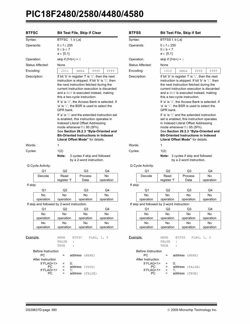
PIC18F2480/2580/4480/4580
BTFSC Bit Test File, Skip if Clear
Syntax: BTFSC f, b ,a
Operands: 0 ≤ f ≤ 2550 ≤ b ≤ 7a ∈ [0,1]
Operation: skip if (f<b>) = 0
Status Affected: None
Encoding: 1011 bbba ffff ffff
Description: If bit ‘b’ in register ‘f’ is ‘0’, then the next instruction is skipped. If bit ‘b’ is ‘0’, then the next instruction fetched during the current instruction execution is discarded and a NOP is executed instead, making this a two-cycle instruction. If ‘a’ is ‘0’, the Access Bank is selected. If ‘a’ is ‘1’, the BSR is used to select the GPR bank. If ‘a’ is ‘0’ and the extended instruction set is enabled, this instruction operates in Indexed Literal Offset Addressing mode whenever f ≤ 95 (5Fh). See Section 26.2.3 “Byte-Oriented and Bit-Oriented Instructions in Indexed Literal Offset Mode” for details.
Words: 1
Cycles: 1(2)Note: 3 cycles if skip and followed
by a 2-word instruction.
Q Cycle Activity:Q1 Q2 Q3 Q4
Decode Readregister ‘f’
Process Data
No operation
If skip:Q1 Q2 Q3 Q4No
operationNo
operationNo
operationNo
operationIf skip and followed by 2-word instruction:
Q1 Q2 Q3 Q4No
operationNo
operationNo
operationNo
operationNo
operationNo
operationNo
operationNo
operation
Example: HEREFALSETRUE
BTFSC::
FLAG, 1, 0
Before InstructionPC = address (HERE)
After InstructionIf FLAG<1> = 0;
PC = address (TRUE)If FLAG<1> = 1;
PC = address (FALSE)
BTFSS Bit Test File, Skip if Set
Syntax: BTFSS f, b ,a
Operands: 0 ≤ f ≤ 2550 ≤ b < 7a ∈ [0,1]
Operation: skip if (f<b>) = 1
Status Affected: None
Encoding: 1010 bbba ffff ffff
Description: If bit ‘b’ in register ‘f’ is ‘1’, then the next instruction is skipped. If bit ‘b’ is ‘1’, then the next instruction fetched during the current instruction execution is discarded and a NOP is executed instead, making this a two-cycle instruction. If ‘a’ is ‘0’, the Access Bank is selected. If ‘a’ is ‘1’, the BSR is used to select the GPR bank. If ‘a’ is ‘0’ and the extended instruction set is enabled, this instruction operates in Indexed Literal Offset Addressing mode whenever f ≤ 95 (5Fh). See Section 26.2.3 “Byte-Oriented and Bit-Oriented Instructions in Indexed Literal Offset Mode” for details.
Words: 1
Cycles: 1(2)Note: 3 cycles if skip and followed
by a 2-word instruction.
Q Cycle Activity:Q1 Q2 Q3 Q4
Decode Readregister ‘f’
Process Data
No operation
If skip:Q1 Q2 Q3 Q4No
operationNo
operationNo
operationNo
operationIf skip and followed by 2-word instruction:
Q1 Q2 Q3 Q4No
operationNo
operationNo
operationNo
operationNo
operationNo
operationNo
operationNo
operation
Example: HEREFALSETRUE
BTFSS::
FLAG, 1, 0
Before InstructionPC = address (HERE)
After InstructionIf FLAG<1> = 0;
PC = address (FALSE)If FLAG<1> = 1;
PC = address (TRUE)
DS39637D-page 380 © 2009 Microchip Technology Inc.

PIC18F2480/2580/4480/4580
BTG Bit Toggle f
Syntax: BTG f, b ,a
Operands: 0 ≤ f ≤ 2550 ≤ b < 7a ∈ [0,1]
Operation: (f<b>) → f<b>
Status Affected: None
Encoding: 0111 bbba ffff ffff
Description: Bit ‘b’ in data memory location ‘f’ is inverted.If ‘a’ is ‘0’, the Access Bank is selected. If ‘a’ is ‘1’, the BSR is used to select the GPR bank. If ‘a’ is ‘0’ and the extended instruction set is enabled, this instruction operates in Indexed Literal Offset Addressing mode whenever f ≤ 95 (5Fh). See Section 26.2.3 “Byte-Oriented and Bit-Oriented Instructions in Indexed Literal Offset Mode” for details.
Words: 1
Cycles: 1
Q Cycle Activity:Q1 Q2 Q3 Q4
Decode Readregister ‘f’
Process Data
Writeregister ‘f’
Example: BTG PORTC, 4, 0
Before Instruction:PORTC = 0111 0101 [75h]
After Instruction:PORTC = 0110 0101 [65h]
BOV Branch if Overflow
Syntax: BOV n
Operands: -128 ≤ n ≤ 127
Operation: if Overflow bit is ‘1’,(PC) + 2 + 2n → PC
Status Affected: None
Encoding: 1110 0100 nnnn nnnn
Description: If the Overflow bit is ‘1’, then the program will branch.The 2’s complement number ‘2n’ is added to the PC. Since the PC will have incremented to fetch the next instruction, the new address will be PC + 2 + 2n. This instruction is then a two-cycle instruction.
Words: 1
Cycles: 1(2)
Q Cycle Activity:If Jump:
Q1 Q2 Q3 Q4Decode Read literal
‘n’Process
DataWrite to PC
No operation
No operation
No operation
No operation
If No Jump:Q1 Q2 Q3 Q4
Decode Read literal ‘n’
Process Data
No operation
Example: HERE BOV Jump
Before InstructionPC = address (HERE)
After InstructionIf Overflow = 1;
PC = address (Jump)If Overflow = 0;
PC = address (HERE + 2)
© 2009 Microchip Technology Inc. DS39637D-page 381

PIC18F2480/2580/4480/4580
BZ Branch if Zero
Syntax: BZ n
Operands: -128 ≤ n ≤ 127
Operation: if Zero bit is ‘1’,(PC) + 2 + 2n → PC
Status Affected: None
Encoding: 1110 0000 nnnn nnnn
Description: If the Zero bit is ‘1’, then the program will branch.The 2’s complement number ‘2n’ is added to the PC. Since the PC will have incremented to fetch the next instruction, the new address will be PC + 2 + 2n. This instruction is then a two-cycle instruction.
Words: 1
Cycles: 1(2)
Q Cycle Activity:If Jump:
Q1 Q2 Q3 Q4Decode Read literal
‘n’Process
DataWrite to PC
No operation
No operation
No operation
No operation
If No Jump:Q1 Q2 Q3 Q4
Decode Read literal ‘n’
Process Data
No operation
Example: HERE BZ Jump
Before InstructionPC = address (HERE)
After InstructionIf Zero = 1;
PC = address (Jump)If Zero = 0;
PC = address (HERE + 2)
CALL Subroutine Call
Syntax: CALL k ,s
Operands: 0 ≤ k ≤ 1048575s ∈ [0,1]
Operation: (PC) + 4 → TOS,k → PC<20:1>;if s = 1,(W) → WS,(STATUS) → STATUSS,(BSR) → BSRS
Status Affected: None
Encoding:1st word (k<7:0>)2nd word(k<19:8>)
11101111
110sk19kkk
k7kkkkkkk
kkkk0kkkk8
Description: Subroutine call of entire 2-Mbyte memory range. First, return address (PC + 4) is pushed onto the return stack. If ‘s’ = 1, the W, STATUS and BSR registers are also pushed into their respective shadow registers, WS, STATUSS and BSRS. If ‘s’ = 0, no update occurs. Then, the 20-bit value ‘k’ is loaded into PC<20:1>. CALL is a two-cycle instruction.
Words: 2
Cycles: 2
Q Cycle Activity:Q1 Q2 Q3 Q4
Decode Read literal ‘k’<7:0>,
Push PC to stack
Read literal ‘k’<19:8>,
Write to PCNo
operationNo
operationNo
operationNo
operation
Example: HERE CALL THERE,1
Before InstructionPC = address (HERE)
After InstructionPC = address (THERE)TOS = address (HERE + 4)WS = WBSRS = BSRSTATUSS= STATUS
DS39637D-page 382 © 2009 Microchip Technology Inc.

PIC18F2480/2580/4480/4580
CLRF Clear f
Syntax: CLRF f ,a
Operands: 0 ≤ f ≤ 255a ∈ [0,1]
Operation: 000h → f,1 → Z
Status Affected: Z
Encoding: 0110 101a ffff ffff
Description: Clears the contents of the specified register. If ‘a’ is ‘0’, the Access Bank is selected. If ‘a’ is ‘1’, the BSR is used to select the GPR bank. If ‘a’ is ‘0’ and the extended instruction set is enabled, this instruction operates in Indexed Literal Offset Addressing mode whenever f ≤ 95 (5Fh). See Section 26.2.3 “Byte-Oriented and Bit-Oriented Instructions in Indexed Literal Offset Mode” for details.
Words: 1
Cycles: 1
Q Cycle Activity:Q1 Q2 Q3 Q4
Decode Readregister ‘f’
Process Data
Writeregister ‘f’
Example: CLRF FLAG_REG,1
Before InstructionFLAG_REG = 5Ah
After InstructionFLAG_REG = 00h
CLRWDT Clear Watchdog Timer
Syntax: CLRWDT
Operands: None
Operation: 000h → WDT,000h → WDT postscaler,1 → TO,1 → PD
Status Affected: TO, PD
Encoding: 0000 0000 0000 0100
Description: CLRWDT instruction resets the Watchdog Timer. It also resets the post-scaler of the WDT. Status bits TO and PD are set.
Words: 1
Cycles: 1
Q Cycle Activity:Q1 Q2 Q3 Q4
Decode No operation
Process Data
No operation
Example: CLRWDT
Before InstructionWDT Counter = ?
After InstructionWDT Counter = 00hWDT Postscaler = 0TO = 1PD = 1
© 2009 Microchip Technology Inc. DS39637D-page 383

PIC18F2480/2580/4480/4580
COMF Complement f
Syntax: COMF f ,d ,a
Operands: 0 ≤ f ≤ 255d ∈ [0,1]a ∈ [0,1]
Operation: → dest
Status Affected: N, Z
Encoding: 0001 11da ffff ffff
Description: The contents of register ‘f’ are complemented. If ‘d’ is ‘1’, the result is stored in W. If ‘d’ is ‘0’, the result is stored back in register ‘f’. If ‘a’ is ‘0’, the Access Bank is selected. If ‘a’ is ‘1’, the BSR is used to select the GPR bank. If ‘a’ is ‘0’ and the extended instruction set is enabled, this instruction operates in Indexed Literal Offset Addressing mode whenever f ≤ 95 (5Fh). See Section 26.2.3 “Byte-Oriented and Bit-Oriented Instructions in Indexed Literal Offset Mode” for details.
Words: 1
Cycles: 1
Q Cycle Activity:Q1 Q2 Q3 Q4
Decode Readregister ‘f’
Process Data
Write todestination
Example: COMF REG, 0, 0
Before InstructionREG = 13h
After InstructionREG = 13hW = ECh
( f )
CPFSEQ Compare f with W, Skip if f = WSyntax: CPFSEQ f ,aOperands: 0 ≤ f ≤ 255
a ∈ [0,1]Operation: (f) – (W),
skip if (f) = (W) (unsigned comparison)
Status Affected: NoneEncoding: 0110 001a ffff ffff
Description: Compares the contents of data memory location ‘f’ to the contents of W by performing an unsigned subtraction.If ‘f’ = W, then the fetched instruction is discarded and a NOP is executed instead, making this a two-cycle instruction. If ‘a’ is ‘0’, the Access Bank is selected. If ‘a’ is ‘0’, the BSR is used to select the GPR bank. If ‘a’ is ‘0’ and the extended instruction set is enabled, this instruction operates in Indexed Literal Offset Addressing mode whenever f ≤ 95 (5Fh). See Section 26.2.3 “Byte-Oriented and Bit-Oriented Instructions in Indexed Literal Offset Mode” for details.
Words: 1Cycles: 1(2)
Note: 3 cycles if skip and followedby a 2-word instruction.
Q Cycle Activity:Q1 Q2 Q3 Q4
Decode Readregister ‘f’
Process Data
No operation
If skip:Q1 Q2 Q3 Q4No
operationNo
operationNo
operationNo
operationIf skip and followed by 2-word instruction:
Q1 Q2 Q3 Q4No
operationNo
operationNo
operationNo
operationNo
operationNo
operationNo
operationNo
operation
Example: HERE CPFSEQ REG, 0NEQUAL :EQUAL :
Before InstructionPC Address = HEREW = ?REG = ?
After InstructionIf REG = W;
PC = Address (EQUAL)If REG ≠ W;
PC = Address (NEQUAL)
DS39637D-page 384 © 2009 Microchip Technology Inc.

PIC18F2480/2580/4480/4580
CPFSGT Compare f with W, Skip if f > WSyntax: CPFSGT f ,aOperands: 0 ≤ f ≤ 255
a ∈ [0,1]Operation: (f) − (W),
skip if (f) > (W) (unsigned comparison)
Status Affected: NoneEncoding: 0110 010a ffff ffff
Description: Compares the contents of data memory location ‘f’ to the contents of the W by performing an unsigned subtraction.If the contents of ‘f’ are greater than the contents of WREG, then the fetched instruction is discarded and a NOP is executed instead, making this a two-cycle instruction. If ‘a’ is ‘0’, the Access Bank is selected. If ‘a’ is ‘1’, the BSR is used to select the GPR bank. If ‘a’ is ‘0’ and the extended instruction set is enabled, this instruction operates in Indexed Literal Offset Addressing mode whenever f ≤ 95 (5Fh). See Section 26.2.3 “Byte-Oriented and Bit-Oriented Instructions in Indexed Literal Offset Mode” for details.
Words: 1Cycles: 1(2)
Note: 3 cycles if skip and followedby a 2-word instruction.
Q Cycle Activity:Q1 Q2 Q3 Q4
Decode Readregister ‘f’
Process Data
No operation
If skip:Q1 Q2 Q3 Q4No
operationNo
operationNo
operationNo
operationIf skip and followed by 2-word instruction:
Q1 Q2 Q3 Q4No
operationNo
operationNo
operationNo
operationNo
operationNo
operationNo
operationNo
operation
Example: HERE CPFSGT REG, 0NGREATER :GREATER :
Before InstructionPC = Address (HERE)W = ?
After InstructionIf REG > W;
PC = Address (GREATER)If REG ≤ W;
PC = Address (NGREATER)
CPFSLT Compare f with W, Skip if f < W
Syntax: CPFSLT f ,a
Operands: 0 ≤ f ≤ 255a ∈ [0,1]
Operation: (f) – (W),skip if (f) < (W) (unsigned comparison)
Status Affected: None
Encoding: 0110 000a ffff ffff
Description: Compares the contents of data memory location ‘f’ to the contents of W by performing an unsigned subtraction.If the contents of ‘f’ are less than the contents of W, then the fetched instruction is discarded and a NOP is executed instead, making this a two-cycle instruction. If ‘a’ is ‘0’, the Access Bank is selected. If ‘a’ is ‘1’, the BSR is used to select the GPR bank.
Words: 1
Cycles: 1(2)Note: 3 cycles if skip and followed
by a 2-word instruction.
Q Cycle Activity:Q1 Q2 Q3 Q4
Decode Readregister ‘f’
Process Data
No operation
If skip:Q1 Q2 Q3 Q4No
operationNo
operationNo
operationNo
operationIf skip and followed by 2-word instruction:
Q1 Q2 Q3 Q4No
operationNo
operationNo
operationNo
operationNo
operationNo
operationNo
operationNo
operation
Example: HERE CPFSLT REG, 1NLESS :LESS :
Before InstructionPC = Address (HERE)W = ?
After InstructionIf REG < W;PC = Address (LESS)If REG ≥ W;PC = Address (NLESS)
© 2009 Microchip Technology Inc. DS39637D-page 385

PIC18F2480/2580/4480/4580
DAW Decimal Adjust W Register
Syntax: DAW
Operands: None
Operation: If [W<3:0> >9] or [DC = 1] then,(W<3:0>) + 6 → W<3:0>;else, (W<3:0>) → W<3:0>;
If [W<7:4> >9] or [C = 1] then,(W<7:4>) + 6 → W<7:4>;C = 1,else, (W<7:4>) → W<7:4>
Status Affected: C
Encoding: 0000 0000 0000 0111
Description: DAW adjusts the eight-bit value in W, resulting from the earlier addition of two variables (each in packed BCD format) and produces a correct packed BCD result.
Words: 1
Cycles: 1
Q Cycle Activity:Q1 Q2 Q3 Q4
Decode Readregister W
Process Data
WriteW
Example 1:DAW
Before InstructionW = A5hC = 0DC = 0
After InstructionW = 05hC = 1DC = 0
Example 2:Before Instruction
W = CEhC = 0DC = 0
After InstructionW = 34hC = 1DC = 0
DECF Decrement f
Syntax: DECF f ,d ,a
Operands: 0 ≤ f ≤ 255d ∈ [0,1]a ∈ [0,1]
Operation: (f) – 1 → dest
Status Affected: C, DC, N, OV, Z
Encoding: 0000 01da ffff ffff
Description: Decrement register ‘f’. If ‘d’ is ‘0’, the result is stored in W. If ‘d’ is ‘1’, the result is stored back in register ‘f’. If ‘a’ is ‘0’, the Access Bank is selected. If ‘a’ is ‘1’, the BSR is used to select the GPR bank. If ‘a’ is ‘0’ and the extended instruction set is enabled, this instruction operates in Indexed Literal Offset Addressing mode whenever f ≤ 95 (5Fh). See Section 26.2.3 “Byte-Oriented and Bit-Oriented Instructions in Indexed Literal Offset Mode” for details.
Words: 1
Cycles: 1
Q Cycle Activity:Q1 Q2 Q3 Q4
Decode Readregister ‘f’
Process Data
Write to destination
Example: DECF CNT, 1, 0
Before InstructionCNT = 01hZ = 0
After InstructionCNT = 00hZ = 1
DS39637D-page 386 © 2009 Microchip Technology Inc.

PIC18F2480/2580/4480/4580
DECFSZ Decrement f, Skip if 0
Syntax: DECFSZ f ,d ,a
Operands: 0 ≤ f ≤ 255d ∈ [0,1]a ∈ [0,1]
Operation: (f) – 1 → dest,skip if result = 0
Status Affected: None
Encoding: 0010 11da ffff ffff
Description: The contents of register ‘f’ are decremented. If ‘d’ is ‘0’, the result is placed in W. If ‘d’ is ‘1’, the result is placed back in register ‘f’.If the result is ‘0’, the next instruction which is already fetched is discarded and a NOP is executed instead, making it a two-cycle instruction.If ‘a’ is ‘0’, the Access Bank is selected. If ‘a’ is ‘1’, the BSR is used to select the GPR bank. If ‘a’ is ‘0’ and the extended instruction set is enabled, this instruction operates in Indexed Literal Offset Addressing mode whenever f ≤ 95 (5Fh). See Section 26.2.3 “Byte-Oriented and Bit-Oriented Instructions in Indexed Literal Offset Mode” for details.
Words: 1
Cycles: 1(2)Note: 3 cycles if skip and followed
by a 2-word instruction.
Q Cycle Activity:Q1 Q2 Q3 Q4
Decode Readregister ‘f’
Process Data
Write to destination
If skip:Q1 Q2 Q3 Q4No
operationNo
operationNo
operationNo
operationIf skip and followed by 2-word instruction:
Q1 Q2 Q3 Q4No
operationNo
operationNo
operationNo
operationNo
operationNo
operationNo
operationNo
operation
Example: HERE DECFSZ CNT, 1, 1 GOTO LOOPCONTINUE
Before InstructionPC = Address (HERE)
After InstructionCNT = CNT – 1If CNT = 0;
PC = Address (CONTINUE)If CNT ≠ 0;
PC = Address (HERE + 2)
DCFSNZ Decrement f, Skip if not 0
Syntax: DCFSNZ f ,d ,a
Operands: 0 ≤ f ≤ 255d ∈ [0,1]a ∈ [0,1]
Operation: (f) – 1 → dest,skip if result ≠ 0
Status Affected: None
Encoding: 0100 11da ffff ffff
Description: The contents of register ‘f’ are decremented. If ‘d’ is ‘0’, the result is placed in W. If ‘d’ is ‘1’, the result is placed back in register ‘f’.If the result is not ‘0’, the next instruction which is already fetched is discarded and a NOP is executed instead, making it a two-cycle instruction. If ‘a’ is ‘0’, the Access Bank is selected. If ‘a’ is ‘1’, the BSR is used to select the GPR bank. If ‘a’ is ‘0’ and the extended instruction set is enabled, this instruction operates in Indexed Literal Offset Addressing mode whenever f ≤ 95 (5Fh). See Section 26.2.3 “Byte-Oriented and Bit-Oriented Instructions in Indexed Literal Offset Mode” for details.
Words: 1
Cycles: 1(2)Note: 3 cycles if skip and followed
by a 2-word instruction.
Q Cycle Activity:Q1 Q2 Q3 Q4
Decode Readregister ‘f’
Process Data
Write to destination
If skip:Q1 Q2 Q3 Q4No
operationNo
operationNo
operationNo
operationIf skip and followed by 2-word instruction:
Q1 Q2 Q3 Q4No
operationNo
operationNo
operationNo
operationNo
operationNo
operationNo
operationNo
operation
Example: HERE DCFSNZ TEMP, 1, 0ZERO : NZERO :
Before InstructionTEMP = ?
After InstructionTEMP = TEMP – 1,If TEMP = 0;
PC = Address (ZERO)If TEMP ≠ 0;
PC = Address (NZERO)
© 2009 Microchip Technology Inc. DS39637D-page 387

PIC18F2480/2580/4480/4580
GOTO Unconditional Branch
Syntax: GOTO k
Operands: 0 ≤ k ≤ 1048575
Operation: k → PC<20:1>
Status Affected: None
Encoding:1st word (k<7:0>)2nd word(k<19:8>)
11101111
1111k19kkk
k7kkkkkkk
kkkk0kkkk8
Description: GOTO allows an unconditional branch anywhere within entire 2-Mbyte memory range. The 20-bit value ‘k’ is loaded into PC<20:1>. GOTO is always a two-cycle instruction.
Words: 2
Cycles: 2
Q Cycle Activity:Q1 Q2 Q3 Q4
Decode Read literal ‘k’<7:0>,
No operation
Read literal ‘k’<19:8>,
Write to PCNo
operationNo
operationNo
operationNo
operation
Example: GOTO THERE
After InstructionPC = Address (THERE)
INCF Increment f
Syntax: INCF f ,d ,a
Operands: 0 ≤ f ≤ 255d ∈ [0,1]a ∈ [0,1]
Operation: (f) + 1 → dest
Status Affected: C, DC, N, OV, Z
Encoding: 0010 10da ffff ffff
Description: The contents of register ‘f’ are incremented. If ‘d’ is ‘0’, the result is placed in W. If ‘d’ is ‘1’, the result is placed back in register ‘f’. If ‘a’ is ‘0’, the Access Bank is selected. If ‘a’ is ‘1’, the BSR is used to select the GPR bank. If ‘a’ is ‘0’ and the extended instruction set is enabled, this instruction operates in Indexed Literal Offset Addressing mode whenever f ≤ 95 (5Fh). See Section 26.2.3 “Byte-Oriented and Bit-Oriented Instructions in Indexed Literal Offset Mode” for details.
Words: 1
Cycles: 1
Q Cycle Activity:Q1 Q2 Q3 Q4
Decode Readregister ‘f’
Process Data
Write to destination
Example: INCF CNT, 1, 0
Before InstructionCNT = FFhZ = 0C = ?DC = ?
After InstructionCNT = 00hZ = 1C = 1DC = 1
DS39637D-page 388 © 2009 Microchip Technology Inc.
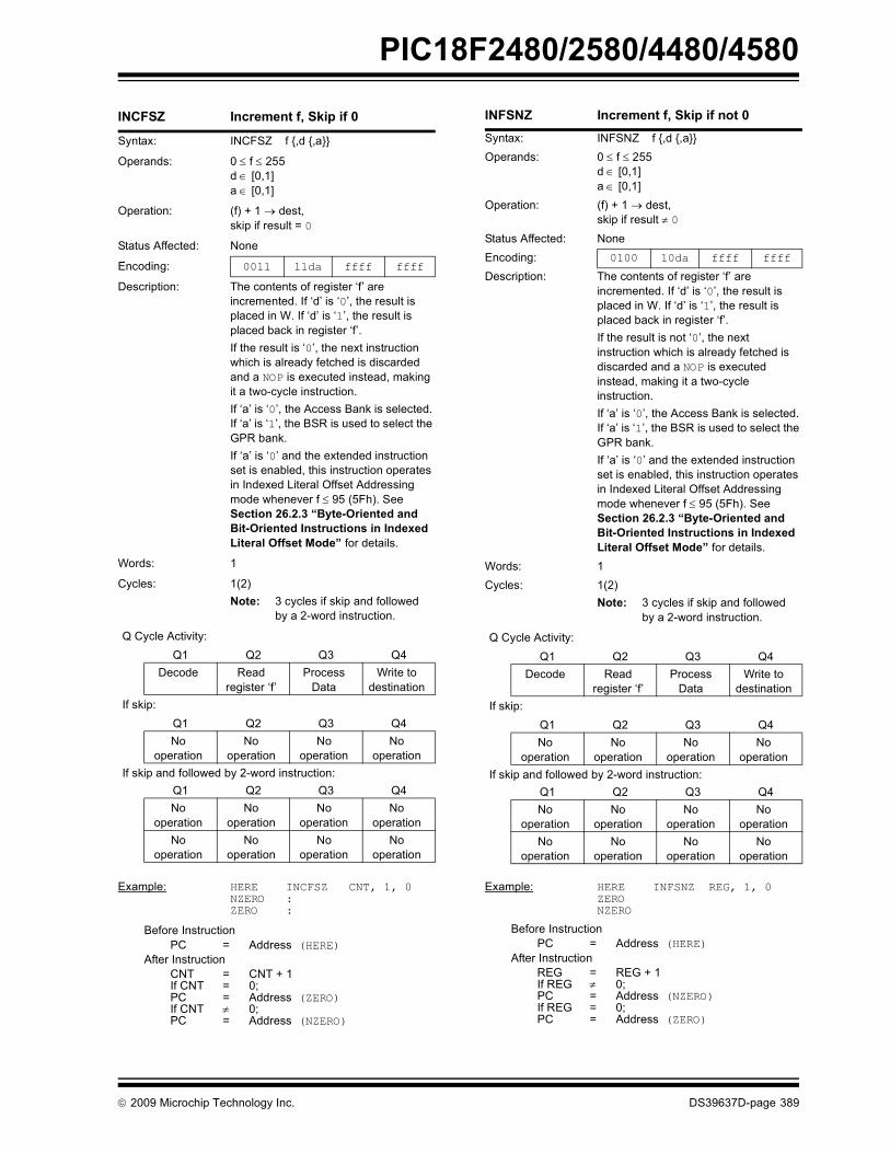
PIC18F2480/2580/4480/4580
INCFSZ Increment f, Skip if 0
Syntax: INCFSZ f ,d ,a
Operands: 0 ≤ f ≤ 255d ∈ [0,1]a ∈ [0,1]
Operation: (f) + 1 → dest,skip if result = 0
Status Affected: None
Encoding: 0011 11da ffff ffff
Description: The contents of register ‘f’ are incremented. If ‘d’ is ‘0’, the result is placed in W. If ‘d’ is ‘1’, the result is placed back in register ‘f’.If the result is ‘0’, the next instruction which is already fetched is discarded and a NOP is executed instead, making it a two-cycle instruction. If ‘a’ is ‘0’, the Access Bank is selected. If ‘a’ is ‘1’, the BSR is used to select the GPR bank. If ‘a’ is ‘0’ and the extended instruction set is enabled, this instruction operates in Indexed Literal Offset Addressing mode whenever f ≤ 95 (5Fh). See Section 26.2.3 “Byte-Oriented and Bit-Oriented Instructions in Indexed Literal Offset Mode” for details.
Words: 1
Cycles: 1(2)Note: 3 cycles if skip and followed
by a 2-word instruction.
Q Cycle Activity:Q1 Q2 Q3 Q4
Decode Readregister ‘f’
Process Data
Write to destination
If skip:Q1 Q2 Q3 Q4No
operationNo
operationNo
operationNo
operationIf skip and followed by 2-word instruction:
Q1 Q2 Q3 Q4No
operationNo
operationNo
operationNo
operationNo
operationNo
operationNo
operationNo
operation
Example: HERE INCFSZ CNT, 1, 0NZERO : ZERO :
Before InstructionPC = Address (HERE)
After InstructionCNT = CNT + 1If CNT = 0;PC = Address (ZERO)If CNT ≠ 0;PC = Address (NZERO)
INFSNZ Increment f, Skip if not 0Syntax: INFSNZ f ,d ,aOperands: 0 ≤ f ≤ 255
d ∈ [0,1]a ∈ [0,1]
Operation: (f) + 1 → dest, skip if result ≠ 0
Status Affected: NoneEncoding: 0100 10da ffff ffff
Description: The contents of register ‘f’ are incremented. If ‘d’ is ‘0’, the result is placed in W. If ‘d’ is ‘1’, the result is placed back in register ‘f’.If the result is not ‘0’, the next instruction which is already fetched is discarded and a NOP is executed instead, making it a two-cycle instruction. If ‘a’ is ‘0’, the Access Bank is selected. If ‘a’ is ‘1’, the BSR is used to select the GPR bank. If ‘a’ is ‘0’ and the extended instruction set is enabled, this instruction operates in Indexed Literal Offset Addressing mode whenever f ≤ 95 (5Fh). See Section 26.2.3 “Byte-Oriented and Bit-Oriented Instructions in Indexed Literal Offset Mode” for details.
Words: 1Cycles: 1(2)
Note: 3 cycles if skip and followedby a 2-word instruction.
Q Cycle Activity:Q1 Q2 Q3 Q4
Decode Readregister ‘f’
Process Data
Write to destination
If skip:Q1 Q2 Q3 Q4No
operationNo
operationNo
operationNo
operationIf skip and followed by 2-word instruction:
Q1 Q2 Q3 Q4No
operationNo
operationNo
operationNo
operationNo
operationNo
operationNo
operationNo
operation
Example: HERE INFSNZ REG, 1, 0ZERONZERO
Before InstructionPC = Address (HERE)
After InstructionREG = REG + 1If REG ≠ 0;PC = Address (NZERO)If REG = 0;PC = Address (ZERO)
© 2009 Microchip Technology Inc. DS39637D-page 389

PIC18F2480/2580/4480/4580
IORLW Inclusive OR Literal with W
Syntax: IORLW k
Operands: 0 ≤ k ≤ 255
Operation: (W) .OR. k → W
Status Affected: N, Z
Encoding: 0000 1001 kkkk kkkk
Description: The contents of W are ORed with the eight-bit literal ‘k’. The result is placed in W.
Words: 1
Cycles: 1
Q Cycle Activity:Q1 Q2 Q3 Q4
Decode Read literal ‘k’
Process Data
Write to W
Example: IORLW 35h
Before InstructionW = 9Ah
After InstructionW = BFh
IORWF Inclusive OR W with f
Syntax: IORWF f ,d ,a
Operands: 0 ≤ f ≤ 255d ∈ [0,1]a ∈ [0,1]
Operation: (W) .OR. (f) → dest
Status Affected: N, Z
Encoding: 0001 00da ffff ffff
Description: Inclusive OR W with register ‘f’. If ‘d’ is ‘0’, the result is placed in W. If ‘d’ is ‘1’, the result is placed back in register ‘f’. If ‘a’ is ‘0’, the Access Bank is selected. If ‘a’ is ‘1’, the BSR is used to select the GPR bank. If ‘a’ is ‘0’ and the extended instruction set is enabled, this instruction operates in Indexed Literal Offset Addressing mode whenever f ≤ 95 (5Fh). See Section 26.2.3 “Byte-Oriented and Bit-Oriented Instructions in Indexed Literal Offset Mode” for details.
Words: 1
Cycles: 1
Q Cycle Activity:Q1 Q2 Q3 Q4
Decode Readregister ‘f’
Process Data
Write to destination
Example: IORWF RESULT, 0, 1
Before InstructionRESULT = 13hW = 91h
After InstructionRESULT = 13hW = 93h
DS39637D-page 390 © 2009 Microchip Technology Inc.

PIC18F2480/2580/4480/4580
LFSR Load FSR
Syntax: LFSR f, k
Operands: 0 ≤ f ≤ 20 ≤ k ≤ 4095
Operation: k → FSRf
Status Affected: None
Encoding: 11101111
11100000
00ffk7kkk
k11kkkkkkk
Description: The 12-bit literal ‘k’ is loaded into the file select register pointed to by ‘f’.
Words: 2
Cycles: 2
Q Cycle Activity:Q1 Q2 Q3 Q4
Decode Read literal ‘k’ MSB
Process Data
Writeliteral ‘k’ MSB to FSRfH
Decode Read literal ‘k’ LSB
Process Data
Write literal ‘k’ to FSRfL
Example: LFSR 2, 3ABh
After InstructionFSR2H = 03hFSR2L = ABh
MOVF Move f
Syntax: MOVF f ,d ,a
Operands: 0 ≤ f ≤ 255d ∈ [0,1]a ∈ [0,1]
Operation: f → dest
Status Affected: N, Z
Encoding: 0101 00da ffff ffff
Description: The contents of register ‘f’ are moved to a destination dependent upon the status of ‘d’. If ‘d’ is ‘0’, the result is placed in W. If ‘d’ is ‘1’, the result is placed back in register ‘f’. Location ‘f’ can be anywhere in the 256-byte bank.If ‘a’ is ‘0’, the Access Bank is selected. If ‘a’ is ‘1’, the BSR is used to select the GPR bank. If ‘a’ is ‘0’ and the extended instruction set is enabled, this instruction operates in Indexed Literal Offset Addressing mode whenever f ≤ 95 (5Fh). See Section 26.2.3 “Byte-Oriented and Bit-Oriented Instructions in Indexed Literal Offset Mode” for details.
Words: 1
Cycles: 1
Q Cycle Activity:Q1 Q2 Q3 Q4
Decode Readregister ‘f’
Process Data
Write W
Example: MOVF REG, 0, 0
Before InstructionREG = 22hW = FFh
After InstructionREG = 22hW = 22h
© 2009 Microchip Technology Inc. DS39637D-page 391

PIC18F2480/2580/4480/4580
MOVFF Move f to f
Syntax: MOVFF fs,fdOperands: 0 ≤ fs ≤ 4095
0 ≤ fd ≤ 4095
Operation: (fs) → fdStatus Affected: None
Encoding:1st word (source)2nd word (destin.)
11001111
ffffffff
ffffffff
ffffsffffd
Description: The contents of source register ‘fs’ are moved to destination register ‘fd’. Location of source ‘fs’ can be anywhere in the 4096-byte data space (000h to FFFh) and location of destination ‘fd’ can also be anywhere from 000h to FFFh.Either source or destination can be W (a useful special situation).MOVFF is particularly useful for transferring a data memory location to a peripheral register (such as the transmit buffer or an I/O port).The MOVFF instruction cannot use the PCL, TOSU, TOSH or TOSL as the destination register.
Words: 2
Cycles: 2 (3)
Q Cycle Activity:Q1 Q2 Q3 Q4
Decode Readregister ‘f’
(src)
Process Data
No operation
Decode No operation
No dummy read
No operation
Write register ‘f’
(dest)
Example: MOVFF REG1, REG2
Before InstructionREG1 = 33hREG2 = 11h
After InstructionREG1 = 33hREG2 = 33h
MOVLB Move Literal to Low Nibble in BSR
Syntax: MOVLW k
Operands: 0 ≤ k ≤ 255
Operation: k → BSR
Status Affected: None
Encoding: 0000 0001 kkkk kkkk
Description: The eight-bit literal ‘k’ is loaded into the Bank Select Register (BSR). The value of BSR<7:4> always remains ‘0’, regardless of the value of k7:k4.
Words: 1
Cycles: 1
Q Cycle Activity:Q1 Q2 Q3 Q4
Decode Readliteral ‘k’
Process Data
Write literal ‘k’ to BSR
Example: MOVLB 5
Before InstructionBSR Register = 02h
After InstructionBSR Register = 05h
DS39637D-page 392 © 2009 Microchip Technology Inc.

PIC18F2480/2580/4480/4580
MOVLW Move Literal to W
Syntax: MOVLW k
Operands: 0 ≤ k ≤ 255
Operation: k → W
Status Affected: None
Encoding: 0000 1110 kkkk kkkk
Description: The eight-bit literal ‘k’ is loaded into W.
Words: 1
Cycles: 1
Q Cycle Activity:Q1 Q2 Q3 Q4
Decode Readliteral ‘k’
Process Data
Write to W
Example: MOVLW 5Ah
After InstructionW = 5Ah
MOVWF Move W to f
Syntax: MOVWF f ,a
Operands: 0 ≤ f ≤ 255a ∈ [0,1]
Operation: (W) → f
Status Affected: None
Encoding: 0110 111a ffff ffff
Description: Move data from W to register ‘f’. Location ‘f’ can be anywhere in the 256-byte bank. If ‘a’ is ‘0’, the Access Bank is selected. If ‘a’ is ‘1’, the BSR is used to select the GPR bank. If ‘a’ is ‘0’ and the extended instruction set is enabled, this instruction operates in Indexed Literal Offset Addressing mode whenever f ≤ 95 (5Fh). See Section 26.2.3 “Byte-Oriented and Bit-Oriented Instructions in Indexed Literal Offset Mode” for details.
Words: 1
Cycles: 1
Q Cycle Activity:Q1 Q2 Q3 Q4
Decode Readregister ‘f’
Process Data
Writeregister ‘f’
Example: MOVWF REG, 0
Before InstructionW = 4FhREG = FFh
After InstructionW = 4FhREG = 4Fh
© 2009 Microchip Technology Inc. DS39637D-page 393

PIC18F2480/2580/4480/4580
MULLW Multiply Literal with W
Syntax: MULLW k
Operands: 0 ≤ k ≤ 255
Operation: (W) x k → PRODH:PRODL
Status Affected: None
Encoding: 0000 1101 kkkk kkkk
Description: An unsigned multiplication is carried out between the contents of W and the 8-bit literal ‘k’. The 16-bit result is placed in the PRODH:PRODL register pair. PRODH contains the high byte.W is unchanged.None of the Status flags are affected.Note that neither overflow nor carry is possible in this operation. A zero result is possible but not detected.
Words: 1
Cycles: 1
Q Cycle Activity:Q1 Q2 Q3 Q4
Decode Read literal ‘k’
Process Data
Write registers PRODH:PRODL
Example: MULLW 0C4h
Before InstructionW = E2hPRODH = ?PRODL = ?
After InstructionW = E2hPRODH = ADhPRODL = 08h
MULWF Multiply W with f
Syntax: MULWF f ,a
Operands: 0 ≤ f ≤ 255a ∈ [0,1]
Operation: (W) x (f) → PRODH:PRODL
Status Affected: None
Encoding: 0000 001a ffff ffff
Description: An unsigned multiplication is carried out between the contents of W and the register file location ‘f’. The 16-bit result is stored in the PRODH:PRODL register pair. PRODH contains the high byte. Both W and ‘f’ are unchanged.None of the Status flags are affected.Note that neither overflow nor carry is possible in this operation. A zero result is possible but not detected.If ‘a’ is ‘0’, the Access Bank is selected. If ‘a’ is ‘1’, the BSR is used to select the GPR bank. If ‘a’ is ‘0’ and the extended instruction set is enabled, this instruction operates in Indexed Literal Offset Addressing mode whenever f ≤ 95 (5Fh). See Section 26.2.3 “Byte-Oriented and Bit-Oriented Instructions in Indexed Literal Offset Mode” for details.
Words: 1
Cycles: 1
Q Cycle Activity:Q1 Q2 Q3 Q4
Decode Readregister ‘f’
Process Data
Writeregisters PRODH:PRODL
Example: MULWF REG, 1
Before InstructionW = C4hREG = B5hPRODH = ?PRODL = ?
After InstructionW = C4hREG = B5hPRODH = 8AhPRODL = 94h
DS39637D-page 394 © 2009 Microchip Technology Inc.

PIC18F2480/2580/4480/4580
NEGF Negate f
Syntax: NEGF f ,a
Operands: 0 ≤ f ≤ 255a ∈ [0,1]
Operation: ( f ) + 1 → f
Status Affected: N, OV, C, DC, Z
Encoding: 0110 110a ffff ffff
Description: Location ‘f’ is negated using two’s complement. The result is placed in the data memory location ‘f’. If ‘a’ is ‘0’, the Access Bank is selected. If ‘a’ is ‘1’, the BSR is used to select the GPR bank. If ‘a’ is ‘0’ and the extended instruction set is enabled, this instruction operates in Indexed Literal Offset Addressing mode whenever f ≤ 95 (5Fh). See Section 26.2.3 “Byte-Oriented and Bit-Oriented Instructions in Indexed Literal Offset Mode” for details.
Words: 1
Cycles: 1
Q Cycle Activity:Q1 Q2 Q3 Q4
Decode Readregister ‘f’
Process Data
Write register ‘f’
Example: NEGF REG, 1
Before InstructionREG = 0011 1010 [3Ah]
After InstructionREG = 1100 0110 [C6h]
NOP No Operation
Syntax: NOP
Operands: None
Operation: No operation
Status Affected: None
Encoding: 00001111
0000xxxx
0000xxxx
0000xxxx
Description: No operation.
Words: 1
Cycles: 1
Q Cycle Activity:Q1 Q2 Q3 Q4
Decode No operation
No operation
No operation
Example:
None.
© 2009 Microchip Technology Inc. DS39637D-page 395

PIC18F2480/2580/4480/4580
POP Pop Top of Return Stack
Syntax: POP
Operands: None
Operation: (TOS) → bit bucket
Status Affected: None
Encoding: 0000 0000 0000 0110
Description: The TOS value is pulled off the return stack and is discarded. The TOS value then becomes the previous value that was pushed onto the return stack.This instruction is provided to enable the user to properly manage the return stack to incorporate a software stack.
Words: 1
Cycles: 1
Q Cycle Activity:Q1 Q2 Q3 Q4
Decode Nooperation
POP TOS value
Nooperation
Example: POPGOTO NEW
Before InstructionTOS = 0031A2hStack (1 level down) = 014332h
After InstructionTOS = 014332hPC = NEW
PUSH Push Top of Return Stack
Syntax: PUSH
Operands: None
Operation: (PC + 2) → TOS
Status Affected: None
Encoding: 0000 0000 0000 0101
Description: The PC + 2 is pushed onto the top of the return stack. The previous TOS value is pushed down on the stack.This instruction allows implementing a software stack by modifying TOS and then pushing it onto the return stack.
Words: 1
Cycles: 1
Q Cycle Activity:Q1 Q2 Q3 Q4
Decode PUSH PC + 2 onto return stack
No operation
No operation
Example: PUSH
Before InstructionTOS = 345AhPC = 0124h
After InstructionPC = 0126hTOS = 0126hStack (1 level down) = 345Ah
DS39637D-page 396 © 2009 Microchip Technology Inc.

PIC18F2480/2580/4480/4580
RCALL Relative Call
Syntax: RCALL n
Operands: -1024 ≤ n ≤ 1023
Operation: (PC) + 2 → TOS,(PC) + 2 + 2n → PC
Status Affected: None
Encoding: 1101 1nnn nnnn nnnn
Description: Subroutine call with a jump up to 1K from the current location. First, return address (PC + 2) is pushed onto the stack. Then, add the 2’s complement number ‘2n’ to the PC. Since the PC will have incremented to fetch the next instruction, the new address will be PC + 2 + 2n. This instruction is a two-cycle instruction.
Words: 1
Cycles: 2
Q Cycle Activity:Q1 Q2 Q3 Q4
Decode Read literal ‘n’
PUSH PC to stack
Process Data
Write to PC
No operation
No operation
No operation
No operation
Example: HERE RCALL Jump
Before InstructionPC = Address (HERE)
After InstructionPC = Address (Jump)TOS = Address (HERE + 2)
RESET Reset
Syntax: RESET
Operands: None
Operation: Reset all registers and flags that are affected by a MCLR Reset.
Status Affected: All
Encoding: 0000 0000 1111 1111
Description: This instruction provides a way to execute a MCLR Reset in software.
Words: 1
Cycles: 1
Q Cycle Activity:Q1 Q2 Q3 Q4
Decode Start Reset
No operation
No operation
Example: RESET
After InstructionRegisters = Reset ValueFlags* = Reset Value
© 2009 Microchip Technology Inc. DS39637D-page 397

PIC18F2480/2580/4480/4580
RETFIE Return from Interrupt
Syntax: RETFIE s
Operands: s ∈ [0,1]
Operation: (TOS) → PC,1 → GIE/GIEH or PEIE/GIEL;if s = 1,(WS) → W,(STATUSS) → STATUS,(BSRS) → BSR,PCLATU, PCLATH are unchanged.
Status Affected: GIE/GIEH, PEIE/GIEL.
Encoding: 0000 0000 0001 000s
Description: Return from interrupt. Stack is popped and Top-of-Stack (TOS) is loaded into the PC. Interrupts are enabled by setting either the high or low-priority global interrupt enable bit. If ‘s’ = 1, the contents of the shadow registers, WS, STATUSS and BSRS, are loaded into their corresponding registers, W, STATUS and BSR. If ‘s’ = 0, no update of these registers occurs.
Words: 1
Cycles: 2
Q Cycle Activity:Q1 Q2 Q3 Q4
Decode No operation
No operation
POP PC from stack
Set GIEH or GIEL
No operation
No operation
No operation
No operation
Example: RETFIE 1
After InterruptPC = TOSW = WSBSR = BSRSSTATUS = STATUSSGIE/GIEH, PEIE/GIEL = 1
RETLW Return Literal to W
Syntax: RETLW k
Operands: 0 ≤ k ≤ 255
Operation: k → W,(TOS) → PC,PCLATU, PCLATH are unchanged
Status Affected: None
Encoding: 0000 1100 kkkk kkkk
Description: W is loaded with the eight-bit literal ‘k’. The program counter is loaded from the top of the stack (the return address). The high address latch (PCLATH) remains unchanged.
Words: 1
Cycles: 2
Q Cycle Activity:Q1 Q2 Q3 Q4
Decode Readliteral ‘k’
Process Data
POP PC from stack, Write to W
No operation
No operation
No operation
No operation
Example: CALL TABLE ; W contains table ; offset value ; W now has ; table value :TABLE
ADDWF PCL ; W = offsetRETLW k0 ; Begin tableRETLW k1 ;
: :
RETLW kn ; End of table
Before InstructionW = 07h
After InstructionW = value of kn
DS39637D-page 398 © 2009 Microchip Technology Inc.

PIC18F2480/2580/4480/4580
RETURN Return from Subroutine
Syntax: RETURN s
Operands: s ∈ [0,1]
Operation: (TOS) → PC;if s = 1,(WS) → W,(STATUSS) → STATUS,(BSRS) → BSR,PCLATU, PCLATH are unchanged
Status Affected: None
Encoding: 0000 0000 0001 001s
Description: Return from subroutine. The stack is popped and the top of the stack (TOS) is loaded into the program counter. If ‘s’= 1, the contents of the shadow registers, WS, STATUSS and BSRS, are loaded into their corresponding registers, W, STATUS and BSR. If ‘s’ = 0, no update of these registers occurs.
Words: 1
Cycles: 2
Q Cycle Activity:Q1 Q2 Q3 Q4
Decode No operation
Process Data
POP PC from stack
No operation
No operation
No operation
No operation
Example: RETURN
After InterruptPC = TOS
RLCF Rotate Left f through Carry
Syntax: RLCF f ,d ,a
Operands: 0 ≤ f ≤ 255d ∈ [0,1]a ∈ [0,1]
Operation: (f<n>) → dest<n + 1>,(f<7>) → C,(C) → dest<0>
Status Affected: C, N, Z
Encoding: 0011 01da ffff ffff
Description: The contents of register ‘f’ are rotated one bit to the left through the Carry flag. If ‘d’ is ‘0’, the result is placed in W. If ‘d’ is ‘1’, the result is stored back in register ‘f’. If ‘a’ is ‘0’, the Access Bank is selected. If ‘a’ is ‘1’, the BSR is used to select the GPR bank. If ‘a’ is ‘0’ and the extended instruction set is enabled, this instruction operates in Indexed Literal Offset Addressing mode whenever f ≤ 95 (5Fh). See Section 26.2.3 “Byte-Oriented and Bit-Oriented Instructions in Indexed Literal Offset Mode” for details.
Words: 1
Cycles: 1
Q Cycle Activity:Q1 Q2 Q3 Q4
Decode Readregister ‘f’
Process Data
Write to destination
Example: RLCF REG, 0, 0
Before InstructionREG = 1110 0110C = 0
After InstructionREG = 1110 0110W = 1100 1100C = 1
C register f
© 2009 Microchip Technology Inc. DS39637D-page 399

PIC18F2480/2580/4480/4580
RLNCF Rotate Left f (No Carry)
Syntax: RLNCF f ,d ,a
Operands: 0 ≤ f ≤ 255d ∈ [0,1]a ∈ [0,1]
Operation: (f<n>) → dest<n + 1>,(f<7>) → dest<0>
Status Affected: N, Z
Encoding: 0100 01da ffff ffff
Description: The contents of register ‘f’ are rotated one bit to the left. If ‘d’ is ‘0’, the result is placed in W. If ‘d’ is ‘1’, the result is stored back in register ‘f’.If ‘a’ is ‘0’, the Access Bank is selected. If ‘a’ is ‘1’, the BSR is used to select the GPR bank. If ‘a’ is ‘0’ and the extended instruction set is enabled, this instruction operates in Indexed Literal Offset Addressing mode whenever f ≤ 95 (5Fh). See Section 26.2.3 “Byte-Oriented and Bit-Oriented Instructions in Indexed Literal Offset Mode” for details.
Words: 1
Cycles: 1
Q Cycle Activity:Q1 Q2 Q3 Q4
Decode Readregister ‘f’
Process Data
Write to destination
Example: RLNCF REG, 1, 0
Before InstructionREG = 1010 1011
After InstructionREG = 0101 0111
register f
RRCF Rotate Right f through Carry
Syntax: RRCF f ,d ,a
Operands: 0 ≤ f ≤ 255d ∈ [0,1]a ∈ [0,1]
Operation: (f<n>) → dest<n – 1>,(f<0>) → C,(C) → dest<7>
Status Affected: C, N, Z
Encoding: 0011 00da ffff ffff
Description: The contents of register ‘f’ are rotated one bit to the right through the Carry flag. If ‘d’ is ‘0’, the result is placed in W. If ‘d’ is ‘1’, the result is placed back in register ‘f’. If ‘a’ is ‘0’, the Access Bank is selected. If ‘a’ is ‘1’, the BSR is used to select the GPR bank. If ‘a’ is ‘0’ and the extended instruction set is enabled, this instruction operates in Indexed Literal Offset Addressing mode whenever f ≤ 95 (5Fh). See Section 26.2.3 “Byte-Oriented and Bit-Oriented Instructions in Indexed Literal Offset Mode” for details.
Words: 1
Cycles: 1
Q Cycle Activity:Q1 Q2 Q3 Q4
Decode Readregister ‘f’
Process Data
Write to destination
Example: RRCF REG, 0, 0
Before InstructionREG = 1110 0110C = 0
After InstructionREG = 1110 0110W = 0111 0011C = 0
C register f
DS39637D-page 400 © 2009 Microchip Technology Inc.
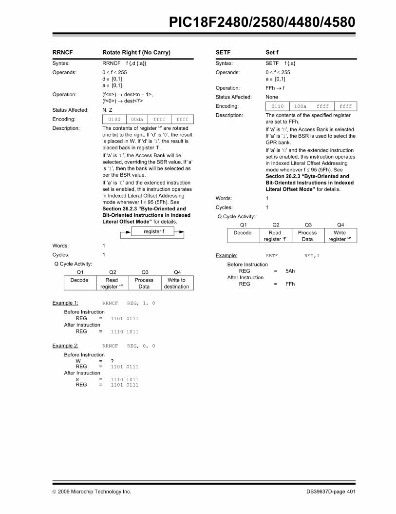
PIC18F2480/2580/4480/4580
RRNCF Rotate Right f (No Carry)
Syntax: RRNCF f ,d ,a
Operands: 0 ≤ f ≤ 255d ∈ [0,1]a ∈ [0,1]
Operation: (f<n>) → dest<n – 1>,(f<0>) → dest<7>
Status Affected: N, Z
Encoding: 0100 00da ffff ffff
Description: The contents of register ‘f’ are rotated one bit to the right. If ‘d’ is ‘0’, the result is placed in W. If ‘d’ is ‘1’, the result is placed back in register ‘f’.If ‘a’ is ‘0’, the Access Bank will be selected, overriding the BSR value. If ‘a’ is ‘1’, then the bank will be selected as per the BSR value.If ‘a’ is ‘0’ and the extended instruction set is enabled, this instruction operates in Indexed Literal Offset Addressing mode whenever f ≤ 95 (5Fh). See Section 26.2.3 “Byte-Oriented and Bit-Oriented Instructions in Indexed Literal Offset Mode” for details.
Words: 1
Cycles: 1
Q Cycle Activity:Q1 Q2 Q3 Q4
Decode Readregister ‘f’
Process Data
Write to destination
Example 1: RRNCF REG, 1, 0
Before InstructionREG = 1101 0111
After InstructionREG = 1110 1011
Example 2: RRNCF REG, 0, 0
Before InstructionW = ?REG = 1101 0111
After InstructionW = 1110 1011REG = 1101 0111
register f
SETF Set f
Syntax: SETF f ,a
Operands: 0 ≤ f ≤ 255a ∈ [0,1]
Operation: FFh → f
Status Affected: None
Encoding: 0110 100a ffff ffff
Description: The contents of the specified register are set to FFh. If ‘a’ is ‘0’, the Access Bank is selected. If ‘a’ is ‘1’, the BSR is used to select the GPR bank. If ‘a’ is ‘0’ and the extended instruction set is enabled, this instruction operates in Indexed Literal Offset Addressing mode whenever f ≤ 95 (5Fh). See Section 26.2.3 “Byte-Oriented and Bit-Oriented Instructions in Indexed Literal Offset Mode” for details.
Words: 1
Cycles: 1
Q Cycle Activity:Q1 Q2 Q3 Q4
Decode Readregister ‘f’
Process Data
Writeregister ‘f’
Example: SETF REG,1
Before InstructionREG = 5Ah
After InstructionREG = FFh
© 2009 Microchip Technology Inc. DS39637D-page 401

PIC18F2480/2580/4480/4580
SLEEP Enter Sleep mode
Syntax: SLEEP
Operands: None
Operation: 00h → WDT,0 → WDT postscaler,1 → TO,0 → PD
Status Affected: TO, PD
Encoding: 0000 0000 0000 0011
Description: The Power-Down Status bit (PD) is cleared. The Time-out Status bit (TO) is set. Watchdog Timer and its postscaler are cleared.The processor is put into Sleep mode with the oscillator stopped.
Words: 1
Cycles: 1
Q Cycle Activity:Q1 Q2 Q3 Q4
Decode No operation
Process Data
Go toSleep
Example: SLEEP
Before InstructionTO = ?PD = ?
After InstructionTO = 1 †PD = 0
† If WDT causes wake-up, this bit is cleared.
SUBFWB Subtract f from W with Borrow
Syntax: SUBFWB f ,d ,a
Operands: 0 ≤ f ≤ 255d ∈ [0,1]a ∈ [0,1]
Operation: (W) – (f) – (C) → dest
Status Affected: N, OV, C, DC, Z
Encoding: 0101 01da ffff ffff
Description: Subtract register ‘f’ and Carry flag (borrow) from W (2’s complement method). If ‘d’ is ‘0’, the result is stored in W. If ‘d’ is ‘1’, the result is stored in register ‘f’. If ‘a’ is ‘0’, the Access Bank is selected. If ‘a’ is ‘1’, the BSR is used to select the GPR bank. If ‘a’ is ‘0’ and the extended instruction set is enabled, this instruction operates in Indexed Literal Offset Addressing mode whenever f ≤ 95 (5Fh). See Section 26.2.3 “Byte-Oriented and Bit-Oriented Instructions in Indexed Literal Offset Mode” for details.
Words: 1
Cycles: 1
Q Cycle Activity:Q1 Q2 Q3 Q4
Decode Readregister ‘f’
Process Data
Write to destination
Example 1: SUBFWB REG, 1, 0
Before InstructionREG = 3W = 2C = 1
After InstructionREG = FFW = 2C = 0Z = 0N = 1 ; result is negative
Example 2: SUBFWB REG, 0, 0Before Instruction
REG = 2W = 5C = 1
After InstructionREG = 2W = 3C = 1Z = 0N = 0 ; result is positive
Example 3: SUBFWB REG, 1, 0
Before InstructionREG = 1W = 2C = 0
After InstructionREG = 0W = 2C = 1Z = 1 ; result is zeroN = 0
DS39637D-page 402 © 2009 Microchip Technology Inc.

PIC18F2480/2580/4480/4580
SUBLW Subtract W from Literal
Syntax: SUBLW k
Operands: 0 ≤ k ≤ 255
Operation: k – (W) → W
Status Affected: N, OV, C, DC, Z
Encoding: 0000 1000 kkkk kkkk
Description: W is subtracted from the eight-bit literal ‘k’. The result is placed in W.
Words: 1
Cycles: 1
Q Cycle Activity:Q1 Q2 Q3 Q4
Decode Readliteral ‘k’
Process Data
Write to W
Example 1: SUBLW 02h
Before InstructionW = 01hC = ?
After InstructionW = 01hC = 1 ; result is positiveZ = 0N = 0
Example 2: SUBLW 02h
Before InstructionW = 02hC = ?
After InstructionW = 00hC = 1 ; result is zeroZ = 1N = 0
Example 3: SUBLW 02h
Before InstructionW = 03hC = ?
After InstructionW = FFh; (2’s complement)C = 0 ; result is negativeZ = 0N = 1
SUBWF Subtract W from f
Syntax: SUBWF f ,d ,a
Operands: 0 ≤ f ≤ 255d ∈ [0,1]a ∈ [0,1]
Operation: (f) – (W) → dest
Status Affected: N, OV, C, DC, Z
Encoding: 0101 11da ffff ffff
Description: Subtract W from register ‘f’ (2’s complement method). If ‘d’ is ‘0’, the result is stored in W. If ‘d’ is ‘1’, the result is stored back in register ‘f’. If ‘a’ is ‘0’, the Access Bank is selected. If ‘a’ is ‘1’, the BSR is used to select the GPR bank. If ‘a’ is ‘0’ and the extended instruction set is enabled, this instruction operates in Indexed Literal Offset Addressing mode whenever f ≤ 95 (5Fh). See Section 26.2.3 “Byte-Oriented and Bit-Oriented Instructions in Indexed Literal Offset Mode” for details.
Words: 1
Cycles: 1
Q Cycle Activity:Q1 Q2 Q3 Q4
Decode Readregister ‘f’
Process Data
Write to destination
Example 1: SUBWF REG, 1, 0
Before InstructionREG = 3W = 2C = ?
After InstructionREG = 1W = 2C = 1 ; result is positiveZ = 0N = 0
Example 2: SUBWF REG, 0, 0
Before InstructionREG = 2W = 2C = ?
After InstructionREG = 2W = 0C = 1 ; result is zeroZ = 1N = 0
Example 3: SUBWF REG, 1, 0
Before InstructionREG = 1W = 2C = ?
After InstructionREG = FFh ;(2’s complement)W = 2C = 0 ; result is negativeZ = 0N = 1
© 2009 Microchip Technology Inc. DS39637D-page 403

PIC18F2480/2580/4480/4580
SUBWFB Subtract W from f with Borrow
Syntax: SUBWFB f ,d ,aOperands: 0 ≤ f ≤ 255
d ∈ [0,1]a ∈ [0,1]
Operation: (f) – (W) – (C) → destStatus Affected: N, OV, C, DC, ZEncoding: 0101 10da ffff ffff
Description: Subtract W and the Carry flag (borrow) from register ‘f’ (2’s complement method). If ‘d’ is ‘0’, the result is stored in W. If ‘d’ is ‘1’, the result is stored back in register ‘f’.If ‘a’ is ‘0’, the Access Bank is selected. If ‘a’ is ‘1’, the BSR is used to select the GPR bank. If ‘a’ is ‘0’ and the extended instruction set is enabled, this instruction operates in Indexed Literal Offset Addressing mode whenever f ≤ 95 (5Fh). See Section 26.2.3 “Byte-Oriented and Bit-Oriented Instructions in Indexed Literal Offset Mode” for details.
Words: 1Cycles: 1Q Cycle Activity:
Q1 Q2 Q3 Q4Decode Read
register ‘f’Process
DataWrite to
destination
Example 1: SUBWFB REG, 1, 0
Before InstructionREG = 19h (0001 1001)W = 0Dh (0000 1101)C = 1
After InstructionREG = 0Ch (0000 1011)W = 0Dh (0000 1101)C = 1Z = 0N = 0 ; result is positive
Example 2: SUBWFB REG, 0, 0
Before InstructionREG = 1Bh (0001 1011)W = 1Ah (0001 1010)C = 0
After InstructionREG = 1Bh (0001 1011)W = 00hC = 1Z = 1 ; result is zeroN = 0
Example 3: SUBWFB REG, 1, 0
Before InstructionREG = 03h (0000 0011)W = 0Eh (0000 1101)C = 1
After InstructionREG = F5h (1111 0100)
; [2’s comp]W = 0Eh (0000 1101)C = 0Z = 0N = 1 ; result is negative
SWAPF Swap f
Syntax: SWAPF f ,d ,a
Operands: 0 ≤ f ≤ 255d ∈ [0,1]a ∈ [0,1]
Operation: (f<3:0>) → dest<7:4>,(f<7:4>) → dest<3:0>
Status Affected: None
Encoding: 0011 10da ffff ffff
Description: The upper and lower nibbles of register ‘f’ are exchanged. If ‘d’ is ‘0’, the result is placed in W. If ‘d’ is ‘1’, the result is placed in register ‘f’.If ‘a’ is ‘0’, the Access Bank is selected. If ‘a’ is ‘1’, the BSR is used to select the GPR bank. If ‘a’ is ‘0’ and the extended instruction set is enabled, this instruction operates in Indexed Literal Offset Addressing mode whenever f ≤ 95 (5Fh). See Section 26.2.3 “Byte-Oriented and Bit-Oriented Instructions in Indexed Literal Offset Mode” for details.
Words: 1
Cycles: 1
Q Cycle Activity:Q1 Q2 Q3 Q4
Decode Readregister ‘f’
Process Data
Write to destination
Example: SWAPF REG, 1, 0
Before InstructionREG = 53h
After InstructionREG = 35h
DS39637D-page 404 © 2009 Microchip Technology Inc.

PIC18F2480/2580/4480/4580
TBLRD Table Read
Syntax: TBLRD ( *; *+; *-; +*)
Operands: None
Operation: if TBLRD *,(Prog Mem (TBLPTR)) → TABLAT,TBLPTR – No Change;if TBLRD *+,(Prog Mem (TBLPTR)) → TABLAT,(TBLPTR) + 1 → TBLPTR;if TBLRD *-,(Prog Mem (TBLPTR)) → TABLAT,(TBLPTR) – 1 → TBLPTR;if TBLRD +*,(TBLPTR) + 1 → TBLPTR,(Prog Mem (TBLPTR)) → TABLAT;
Status Affected: None
Encoding: 0000 0000 0000 10nn nn=0 * =1 *+ =2 *- =3 +*
Description: This instruction is used to read the contents of Program Memory (P.M.). To address the program memory, a pointer, called Table Pointer (TBLPTR), is used.The TBLPTR (a 21-bit pointer) points to each byte in the program memory. TBLPTR has a 2-Mbyte address range.
TBLPTR[0] = 0: Least Significant Byte of Program Memory Word
TBLPTR[0] = 1: Most Significant Byte of Program Memory Word
The TBLRD instruction can modify the value of TBLPTR as follows:• no change• post-increment• post-decrement• pre-increment
Words: 1
Cycles: 2
Q Cycle Activity:Q1 Q2 Q3 Q4
Decode No operation
No operation
No operation
No operation
No operation(Read Program
Memory)
No operation
No operation(Write TABLAT)
TBLRD Table Read (Continued)
Example 1: TBLRD *+ ;
Before InstructionTABLAT = 55hTBLPTR = 00A356hMEMORY(00A356h) = 34h
After InstructionTABLAT = 34hTBLPTR = 00A357h
Example 2: TBLRD +* ;
Before InstructionTABLAT = 0AAhTBLPTR = 01A357hMEMORY(01A357h) = 12hMEMORY(01A358h) = 34h
After InstructionTABLAT = 34hTBLPTR = 01A358h
© 2009 Microchip Technology Inc. DS39637D-page 405

PIC18F2480/2580/4480/4580
TBLWT Table WriteSyntax: TBLWT ( *; *+; *-; +*)Operands: NoneOperation: if TBLWT*,
(TABLAT) → Holding Register,TBLPTR – No Change;if TBLWT*+,(TABLAT) → Holding Register,(TBLPTR) + 1 → TBLPTR;if TBLWT*-,(TABLAT) → Holding Register,(TBLPTR) – 1 → TBLPTR;if TBLWT+*,(TBLPTR) + 1 → TBLPTR,(TABLAT) → Holding Register;
Status Affected: NoneEncoding: 0000 0000 0000 11nn
nn=0 * =1 *+ =2 *- =3 +*
Description: This instruction uses the 3 LSBs of the TBLPTR to determine which of the 8 holding registers the TABLAT is written to. The holding registers are used to pro-gram the contents of Program Memory (P.M.). (Refer to Section 7.0 “Flash Pro-gram Memory” for additional details on programming Flash memory.)The TBLPTR (a 21-bit pointer) points to each byte in the program memory. TBLPTR has a 2-MBtye address range. The LSb of the TBLPTR selects which byte of the program memory location to access.
TBLPTR[0] = 0: Least Significant Byte of Program Memory Word
TBLPTR[0] = 1: Most Significant Byte of Program Memory Word
The TBLWT instruction can modify the value of TBLPTR as follows:• no change• post-increment• post-decrement• pre-increment
Words: 1Cycles: 2 Q Cycle Activity:
Q1 Q2 Q3 Q4Decode No
operationNo
operationNo
operationNo
operationNo
operation(Read
TABLAT)
No operation
No operation(Write to Holding
Register )
TBLWT Table Write (Continued)
Example 1: TBLWT *+;
Before InstructionTABLAT = 55hTBLPTR = 00A356hHOLDING REGISTER (00A356h) = FFh
After Instructions (table write completion)TABLAT = 55hTBLPTR = 00A357hHOLDING REGISTER (00A356h) = 55h
Example 2: TBLWT +*;
Before InstructionTABLAT = 34hTBLPTR = 01389AhHOLDING REGISTER (01389Ah) = FFhHOLDING REGISTER (01389Bh) = FFh
After Instruction (table write completion)TABLAT = 34hTBLPTR = 01389BhHOLDING REGISTER (01389Ah) = FFhHOLDING REGISTER (01389Bh) = 34h
DS39637D-page 406 © 2009 Microchip Technology Inc.

PIC18F2480/2580/4480/4580
TSTFSZ Test f, Skip if 0
Syntax: TSTFSZ f ,a
Operands: 0 ≤ f ≤ 255a ∈ [0,1]
Operation: skip if f = 0
Status Affected: None
Encoding: 0110 011a ffff ffff
Description: If ‘f’ = 0, the next instruction fetched during the current instruction execution is discarded and a NOP is executed, making this a two-cycle instruction. If ‘a’ is ‘0’, the Access Bank is selected. If ‘a’ is ‘1’, the BSR is used to select the GPR bank. If ‘a’ is ‘0’ and the extended instruction set is enabled, this instruction operates in Indexed Literal Offset Addressing mode whenever f ≤ 95 (5Fh). See Section 26.2.3 “Byte-Oriented and Bit-Oriented Instructions in Indexed Literal Offset Mode” for details.
Words: 1
Cycles: 1(2)Note: 3 cycles if skip and followed
by a 2-word instruction.
Q Cycle Activity:Q1 Q2 Q3 Q4
Decode Readregister ‘f’
Process Data
No operation
If skip:Q1 Q2 Q3 Q4No
operationNo
operationNo
operationNo
operationIf skip and followed by 2-word instruction:
Q1 Q2 Q3 Q4No
operationNo
operationNo
operationNo
operationNo
operationNo
operationNo
operationNo
operation
Example: HERE TSTFSZ CNT, 1NZERO :ZERO :
Before InstructionPC = Address (HERE)
After InstructionIf CNT = 00h,PC = Address (ZERO)If CNT ≠ 00h,PC = Address (NZERO)
XORLW Exclusive OR Literal with W
Syntax: XORLW k
Operands: 0 ≤ k ≤ 255
Operation: (W) .XOR. k → W
Status Affected: N, Z
Encoding: 0000 1010 kkkk kkkk
Description: The contents of W are XORed with the 8-bit literal ‘k’. The result is placed in W.
Words: 1
Cycles: 1
Q Cycle Activity:Q1 Q2 Q3 Q4
Decode Readliteral ‘k’
Process Data
Write to W
Example: XORLW 0AFh
Before InstructionW = B5h
After InstructionW = 1Ah
© 2009 Microchip Technology Inc. DS39637D-page 407
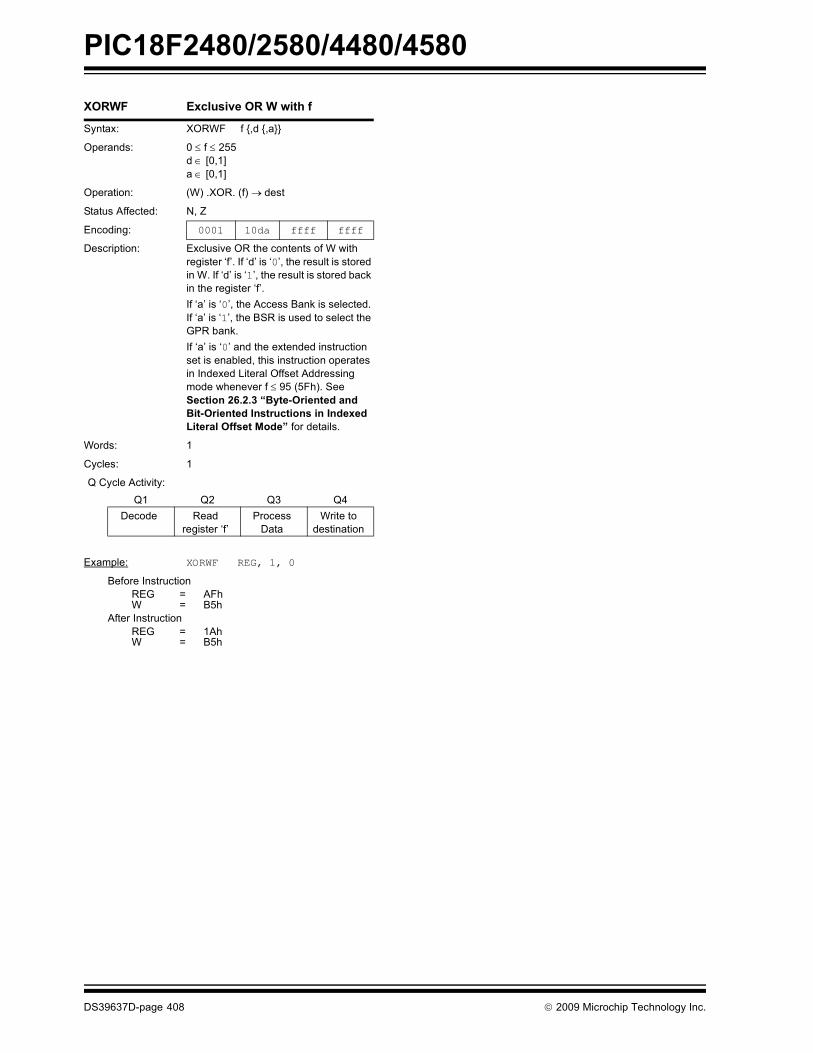
PIC18F2480/2580/4480/4580
XORWF Exclusive OR W with f
Syntax: XORWF f ,d ,a
Operands: 0 ≤ f ≤ 255d ∈ [0,1]a ∈ [0,1]
Operation: (W) .XOR. (f) → dest
Status Affected: N, Z
Encoding: 0001 10da ffff ffff
Description: Exclusive OR the contents of W with register ‘f’. If ‘d’ is ‘0’, the result is stored in W. If ‘d’ is ‘1’, the result is stored back in the register ‘f’. If ‘a’ is ‘0’, the Access Bank is selected. If ‘a’ is ‘1’, the BSR is used to select the GPR bank. If ‘a’ is ‘0’ and the extended instruction set is enabled, this instruction operates in Indexed Literal Offset Addressing mode whenever f ≤ 95 (5Fh). See Section 26.2.3 “Byte-Oriented and Bit-Oriented Instructions in Indexed Literal Offset Mode” for details.
Words: 1
Cycles: 1
Q Cycle Activity:Q1 Q2 Q3 Q4
Decode Readregister ‘f’
Process Data
Write to destination
Example: XORWF REG, 1, 0
Before InstructionREG = AFhW = B5h
After InstructionREG = 1AhW = B5h
DS39637D-page 408 © 2009 Microchip Technology Inc.

PIC18F2480/2580/4480/4580
26.2 Extended Instruction SetIn addition to the standard 75 instructions of the PIC18instruction set, PIC18F2480/2580/4480/4580 devicesalso provide an optional extension to the core CPUfunctionality. The added features include eight addi-tional instructions that augment indirect and indexedaddressing operations and the implementation ofIndexed Literal Offset Addressing mode for many of thestandard PIC18 instructions.The additional features are disabled by default. Toenable them, users must set the XINST Configurationbit.
The instructions in the extended set can all beclassified as literal operations, which either manipulatethe File Select Registers or use them for indexedaddressing. Two of the instructions, ADDFSR andSUBFSR, each have an additional special instantiationfor using FSR2. These versions (ADDULNK andSUBULNK) allow for automatic return after execution.
The extended instructions are specifically implementedto optimize re-entrant program code (that is, code thatis recursive or that uses a software stack) written inhigh-level languages, particularly C. Among otherthings, they allow users working in high-levellanguages to perform certain operations on datastructures more efficiently. These include:
• dynamic allocation and de-allocation of software stack space when entering and leaving subroutines
• function pointer invocation• software Stack Pointer manipulation• manipulation of variables located in a software
stack
A summary of the instructions in the extended instruc-tion set is provided in Table 26-3. Detailed descriptionsare provided in Section 26.2.2 “Extended InstructionSet”. The opcode field descriptions in Table 26-1 applyto both the standard and extended PIC18 instructionsets.
26.2.1 EXTENDED INSTRUCTION SYNTAXMost of the extended instructions use indexed argu-ments, using one of the File Select Registers and someoffset to specify a source or destination register. Whenan argument for an instruction serves as part ofindexed addressing, it is enclosed in square brackets(“[ ]”). This is done to indicate that the argument is usedas an index or offset. MPASM™ Assembler will flag anerror if it determines that an index or offset value is notbracketed.
When the extended instruction set is enabled, bracketsare also used to indicate index arguments in byte-oriented and bit-oriented instructions. This is in additionto other changes in their syntax. For more details, seeSection 26.2.3.1 “Extended Instruction Syntax withStandard PIC18 Commands”.
TABLE 26-3: EXTENSIONS TO THE PIC18 INSTRUCTION SET
Note: The instruction set extension and theIndexed Literal Offset Addressing modewere designed for optimizing applicationswritten in C; the user may likely never usethese instructions directly in assembler.The syntax for these commands is pro-vided as a reference for users who may bereviewing code that has been generatedby a compiler.
Note: In the past, square brackets have beenused to denote optional arguments in thePIC18 and earlier instruction sets. In thistext and going forward, optional argumentsare denoted by braces (“ ”).
Mnemonic,Operands Description Cycles
16-Bit Instruction Word StatusAffectedMSb LSb
ADDFSRADDULNKCALLWMOVSF
MOVSS
PUSHL
SUBFSRSUBULNK
f, kk
zs, fd
zs, zd
k
f, kk
Add Literal to FSRAdd Literal to FSR2 and ReturnCall Subroutine using WREGMove zs (source) to 1st word
fd (destination) 2nd wordMove zs (source) to 1st word
zd (destination) 2nd wordStore Literal at FSR2, Decrement FSR2Subtract Literal from FSRSubtract Literal from FSR2 and Return
1222
2
1
12
11101110000011101111111011111110
11101110
1000100000001011ffff1011xxxx1010
10011001
ffkk 11kk 00010zzzffff1zzzxzzzkkkk
ffkk11kk
kkkkkkkk0100zzzzffffzzzzzzzzkkkk
kkkkkkkk
NoneNoneNoneNone
None
None
NoneNone
© 2009 Microchip Technology Inc. DS39637D-page 409

PIC18F2480/2580/4480/4580
26.2.2 EXTENDED INSTRUCTION SETADDFSR Add Literal to FSR Syntax: ADDFSR f, kOperands: 0 ≤ k ≤ 63
f ∈ [ 0, 1, 2 ]Operation: FSR(f) + k → FSR(f)Status Affected: NoneEncoding: 1110 1000 ffkk kkkk
Description: The 6-bit literal ‘k’ is added to the contents of the FSR specified by ‘f’.
Words: 1Cycles: 1Q Cycle Activity:
Q1 Q2 Q3 Q4Decode Read
literal ‘k’Process
DataWrite to
FSR
Example: ADDFSR 2, 23h
Before InstructionFSR2 = 03FFh
After InstructionFSR2 = 0422h
ADDULNK Add Literal to FSR2 and ReturnSyntax: ADDULNK kOperands: 0 ≤ k ≤ 63Operation: FSR2 + k → FSR2,
PC = (TOS)Status Affected: NoneEncoding: 1110 1000 11kk kkkk
Description: The 6-bit literal ‘k’ is added to the contents of FSR2. A RETURN is then executed by loading the PC with the TOS. The instruction takes two cycles to execute; a NOP is performed during the second cycle.This may be thought of as a special case of the ADDFSR instruction, where f = 3 (binary ‘11’); it operates only on FSR2.
Words: 1Cycles: 2
Q Cycle Activity:Q1 Q2 Q3 Q4
Decode Readliteral ‘k’
Process Data
Write to FSR
No Operation
No Operation
No Operation
No Operation
Example: ADDULNK 23h
Before InstructionFSR2 = 03FFhPC = 0100hTOS = 02AFh
After InstructionFSR2 = 0422hPC = 02AFhTOS = TOS – 1
Note: All PIC18 instructions may take an optional label argument preceding the instruction mnemonic for use insymbolic addressing. If a label is used, the instruction syntax then becomes: label instruction argument(s).
DS39637D-page 410 © 2009 Microchip Technology Inc.

PIC18F2480/2580/4480/4580
CALLW Subroutine Call Using WREG
Syntax: CALLW
Operands: None
Operation: (PC + 2) → TOS,(W) → PCL,(PCLATH) → PCH,(PCLATU) → PCU
Status Affected: None
Encoding: 0000 0000 0001 0100
Description First, the return address (PC + 2) is pushed onto the return stack. Next, the contents of W are written to PCL; the existing value is discarded. Then, the contents of PCLATH and PCLATU are latched into PCH and PCU, respectively. The second cycle is executed as a NOP instruction while the new next instruction is fetched.Unlike CALL, there is no option to update W, STATUS or BSR.
Words: 1
Cycles: 2
Q Cycle Activity:Q1 Q2 Q3 Q4
Decode Read WREG
Push PC to stack
No operation
No operation
No operation
No operation
No operation
Example: HERE CALLW
Before InstructionPC = address (HERE)PCLATH = 10hPCLATU = 00hW = 06h
After InstructionPC = 001006hTOS = address (HERE + 2)PCLATH = 10hPCLATU = 00hW = 06h
MOVSF Move Indexed to f
Syntax: MOVSF [zs], fdOperands: 0 ≤ zs ≤ 127
0 ≤ fd ≤ 4095
Operation: ((FSR2) + zs) → fdStatus Affected: None
Encoding:1st word (source)2nd word (destin.)
11101111
1011ffff
0zzzffff
zzzzsffffd
Description: The contents of the source register are moved to destination register ‘fd’. The actual address of the source register is determined by adding the 7-bit literal offset ‘zs’ in the first word to the value of FSR2. The address of the destination register is specified by the 12-bit literal ‘fd’ in the second word. Both addresses can be anywhere in the 4096-byte data space (000h to FFFh).The MOVSF instruction cannot use the PCL, TOSU, TOSH or TOSL as the destination register.If the resultant source address points to an indirect addressing register, the value returned will be 00h.
Words: 2
Cycles: 2
Q Cycle Activity:Q1 Q2 Q3 Q4
Decode Determine source addr
Determinesource addr
Read source reg
Decode No operation
No dummy read
No operation
Write register ‘f’
(dest)
Example: MOVSF [05h], REG2
Before InstructionFSR2 = 80hContents of 85h = 33hREG2 = 11h
After InstructionFSR2 = 80hContentsof 85h = 33hREG2 = 33h
© 2009 Microchip Technology Inc. DS39637D-page 411

PIC18F2480/2580/4480/4580
MOVSS Move Indexed to IndexedSyntax: MOVSS [zs], [zd]Operands: 0 ≤ zs ≤ 127
0 ≤ zd ≤ 127Operation: ((FSR2) + zs) → ((FSR2) + zd)Status Affected: NoneEncoding:1st word (source)2nd word (dest.)
11101111
1011xxxx
1zzzxzzz
zzzzszzzzd
Description The contents of the source register are moved to the destination register. The addresses of the source and destination registers are determined by adding the 7-bit literal offsets ‘zs’ or ‘zd’, respectively, to the value of FSR2. Both registers can be located anywhere in the 4096-byte data memory space (000h to FFFh).The MOVSS instruction cannot use the PCL, TOSU, TOSH or TOSL as the destination register.If the resultant source address points to an indirect addressing register, the value returned will be 00h. If the resultant destination address points to an indirect addressing register, the instruction will execute as a NOP.
Words: 2Cycles: 2Q Cycle Activity:
Q1 Q2 Q3 Q4Decode Determine
source addrDetermine
source addrRead
source regDecode Determine
dest addrDeterminedest addr
Write to dest reg
Example: MOVSS [05h], [06h]
Before InstructionFSR2 = 80hContentsof 85h = 33hContentsof 86h = 11h
After InstructionFSR2 = 80hContentsof 85h = 33hContentsof 86h = 33h
PUSHL Store Literal at FSR2, Decrement FSR2
Syntax: PUSHL k
Operands: 0 ≤ k ≤ 255
Operation: k → (FSR2),FSR2 – 1→ FSR2
Status Affected: None
Encoding: 1111 1010 kkkk kkkk
Description: The 8-bit literal ‘k’ is written to the data memory address specified by FSR2. FSR2 is decremented by 1 after the operation. This instruction allows users to push values onto a software stack.
Words: 1
Cycles: 1
Q Cycle Activity:Q1 Q2 Q3 Q4
Decode Read ‘k’ Processdata
Write todestination
Example: PUSHL 08h
Before InstructionFSR2H:FSR2L = 01EChMemory (01ECh) = 00h
After InstructionFSR2H:FSR2L = 01EBhMemory (01ECh) = 08h
DS39637D-page 412 © 2009 Microchip Technology Inc.

PIC18F2480/2580/4480/4580
SUBFSR Subtract Literal from FSR Syntax: SUBFSR f, kOperands: 0 ≤ k ≤ 63
f ∈ [ 0, 1, 2 ]Operation: FSRf – k → FSRfStatus Affected: NoneEncoding: 1110 1001 ffkk kkkk
Description: The 6-bit literal ‘k’ is subtracted from the contents of the FSR specified by ‘f’.
Words: 1Cycles: 1Q Cycle Activity:
Q1 Q2 Q3 Q4Decode Read
register ‘f’Process
DataWrite to
destination
Example: SUBFSR 2, 23h
Before InstructionFSR2 = 03FFh
After InstructionFSR2 = 03DCh
SUBULNK Subtract Literal from FSR2 and ReturnSyntax: SUBULNK kOperands: 0 ≤ k ≤ 63Operation: FSR2 – k → FSR2
(TOS) → PCStatus Affected: NoneEncoding: 1110 1001 11kk kkkk
Description: The 6-bit literal ‘k’ is subtracted from the contents of the FSR2. A RETURN is then executed by loading the PC with the TOS. The instruction takes two cycles to execute; a NOP is performed during the second cycle.This may be thought of as a special case of the SUBFSR instruction, where f = 3 (binary ‘11’); it operates only on FSR2.
Words: 1Cycles: 2Q Cycle Activity:
Q1 Q2 Q3 Q4Decode Read
register ‘f’Process
DataWrite to
destinationNo
OperationNo
OperationNo
OperationNo
Operation
Example: SUBULNK 23h
Before InstructionFSR2 = 03FFhPC = 0100h
After InstructionFSR2 = 03DChPC = (TOS)
© 2009 Microchip Technology Inc. DS39637D-page 413

PIC18F2480/2580/4480/4580
26.2.3 BYTE-ORIENTED ANDBIT-ORIENTED INSTRUCTIONS IN INDEXED LITERAL OFFSET MODE
In addition to eight new commands in the extended set,enabling the extended instruction set also enablesIndexed Literal Offset Addressing mode (Section 6.6.1“Indexed Addressing with Literal Offset”). This hasa significant impact on the way that many commands ofthe standard PIC18 instruction set are interpreted.
When the extended set is disabled, addresses embed-ded in opcodes are treated as literal memory locations:either as a location in the Access Bank (a = 0), or in aGPR bank designated by the BSR (a = 1). When theextended instruction set is enabled and a = 0, however,a file register argument of 5Fh or less is interpreted asan offset from the pointer value in FSR2 and not as aliteral address. For practical purposes, this means thatall instructions that use the Access RAM bit as anargument – that is, all byte-oriented and bit-orientedinstructions, or almost half of the core PIC18 instructions– may behave differently when the extended instructionset is enabled.
When the content of FSR2 is 00h, the boundaries of theAccess RAM are essentially remapped to their originalvalues. This may be useful in creating backwardcompatible code. If this technique is used, it may benecessary to save the value of FSR2 and restore itwhen moving back and forth between ‘C’ and assemblyroutines in order to preserve the Stack Pointer. Usersmust also keep in mind the syntax requirements of theextended instruction set (see Section 26.2.3.1“Extended Instruction Syntax with Standard PIC18Commands”).
Although the Indexed Literal Offset Addressing modecan be very useful for dynamic stack and pointermanipulation, it can also be very annoying if a simplearithmetic operation is carried out on the wrongregister. Users who are accustomed to the PIC18programming must keep in mind that, when theextended instruction set is enabled, register addressesof 5Fh or less are used for Indexed Literal OffsetAddressing.
Representative examples of typical byte-oriented andbit-oriented instructions in the Indexed Literal OffsetAddressing mode are provided on the following page toshow how execution is affected. The operandconditions shown in the examples are applicable to allinstructions of these types.
26.2.3.1 Extended Instruction Syntax with Standard PIC18 Commands
When the extended instruction set is enabled, the fileregister argument, ‘f’, in the standard byte-oriented andbit-oriented commands is replaced with the literal offsetvalue, ‘k’. As already noted, this occurs only when ‘f’ isless than or equal to 5Fh. When an offset value is used,it must be indicated by square brackets (“[ ]”). As withthe extended instructions, the use of brackets indicatesto the compiler that the value is to be interpreted as anindex or an offset. Omitting the brackets, or using avalue greater than 5Fh within brackets, will generate anerror in the MPASM™ Assembler.
If the index argument is properly bracketed for IndexedLiteral Offset Addressing, the Access RAM argument isnever specified; it will automatically be assumed to be‘0’. This is in contrast to standard operation (extendedinstruction set disabled) when ‘a’ is set on the basis ofthe target address. Declaring the Access RAM bit inthis mode will also generate an error in the MPASMAssembler.
The destination argument, ‘d’, functions as before.
In the latest versions of the MPASM assembler,language support for the extended instruction set mustbe explicitly invoked. This is done with either thecommand line option, /y, or the PE directive in thesource listing.
26.2.4 CONSIDERATIONS WHEN ENABLING THE EXTENDED INSTRUCTION SET
It is important to note that the extensions to the instruc-tion set may not be beneficial to all users. In particular,users who are not writing code that uses a softwarestack may not benefit from using the extensions to theinstruction set.
Additionally, the Indexed Literal Offset Addressingmode may create issues with legacy applicationswritten to the PIC18 assembler. This is becauseinstructions in the legacy code may attempt to addressregisters in the Access Bank below 5Fh. Since theseaddresses are interpreted as literal offsets to FSR2when the instruction set extension is enabled, theapplication may read or write to the wrong dataaddresses.
When porting an application to the PIC18F2480/2580/4480/4580, it is very important to consider the type ofcode. A large, re-entrant application that is written in ‘C’and would benefit from efficient compilation will do wellwhen using the instruction set extensions. Legacyapplications that heavily use the Access Bank will mostlikely not benefit from using the extended instructionset.
Note: Enabling the PIC18 instruction setextension may cause legacy applicationsto behave erratically or fail entirely.
DS39637D-page 414 © 2009 Microchip Technology Inc.
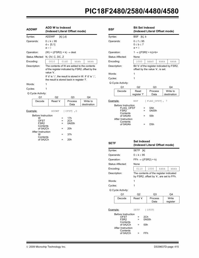
PIC18F2480/2580/4480/4580
ADDWF ADD W to Indexed(Indexed Literal Offset mode)
Syntax: ADDWF [k] ,d
Operands: 0 ≤ k ≤ 95d ∈ [0,1]a = 0
Operation: (W) + ((FSR2) + k) → dest
Status Affected: N, OV, C, DC, Z
Encoding: 0010 01d0 kkkk kkkk
Description: The contents of W are added to the contents of the register indicated by FSR2, offset by the value ‘k’. If ‘d’ is ‘0’, the result is stored in W. If ‘d’ is ‘1’, the result is stored back in register ‘f’.
Words: 1
Cycles: 1
Q Cycle Activity:Q1 Q2 Q3 Q4
Decode Read ‘k’ Process Data
Write todestination
Example: ADDWF [OFST] ,0
Before InstructionW = 17hOFST = 2ChFSR2 = 0A00hContentsof 0A2Ch = 20h
After InstructionW = 37hContentsof 0A2Ch = 20h
BSF Bit Set Indexed (Indexed Literal Offset mode)
Syntax: BSF [k], b
Operands: 0 ≤ f ≤ 950 ≤ b ≤ 7a = 0
Operation: 1 → ((FSR2 + k))<b>
Status Affected: None
Encoding: 1000 bbb0 kkkk kkkk
Description: Bit ‘b’ of the register indicated by FSR2, offset by the value ‘k’, is set.
Words: 1
Cycles: 1
Q Cycle Activity:Q1 Q2 Q3 Q4
Decode Readregister ‘f’
Process Data
Write todestination
Example: BSF [FLAG_OFST], 7
Before InstructionFLAG_OFST = 0AhFSR2 = 0A00hContents of 0A0Ah = 55h
After InstructionContentsof 0A0Ah = D5h
SETF Set Indexed(Indexed Literal Offset mode)
Syntax: SETF [k]
Operands: 0 ≤ k ≤ 95
Operation: FFh → ((FSR2) + k)
Status Affected: None
Encoding: 0110 1000 kkkk kkkk
Description: The contents of the register indicated by FSR2, offset by ‘k’, are set to FFh.
Words: 1
Cycles: 1
Q Cycle Activity:Q1 Q2 Q3 Q4
Decode Read ‘k’ Process Data
Writeregister
Example: SETF [OFST]
Before InstructionOFST = 2ChFSR2 = 0A00hContentsof 0A2Ch = 00h
After InstructionContentsof 0A2Ch = FFh
© 2009 Microchip Technology Inc. DS39637D-page 415

PIC18F2480/2580/4480/4580
26.2.5 SPECIAL CONSIDERATIONS WITHMICROCHIP MPLAB® IDE TOOLS
The latest versions of Microchip’s software tools havebeen designed to fully support the extended instructionset of the PIC18F2480/2580/4480/4580 family ofdevices. This includes the MPLAB C18 C compiler,MPASM assembly language and MPLAB IntegratedDevelopment Environment (IDE).
When selecting a target device for software develop-ment, MPLAB IDE will automatically set default Config-uration bits for that device. The default setting for theXINST Configuration bit is ‘0’, disabling the extendedinstruction set and Indexed Literal Offset Addressingmode. For proper execution of applications developedto take advantage of the extended instruction set,XINST must be set during programming.
To develop software for the extended instruction set,the user must enable support for the instructions andthe Indexed Addressing mode in their language tool(s).Depending on the environment being used, this may bedone in several ways:
• A menu option, or dialog box within the environment, that allows the user to configure the language tool and its settings for the project
• A command line option• A directive in the source code
These options vary between different compilers,assemblers and development environments. Users areencouraged to review the documentation accompany-ing their development systems for the appropriateinformation.
DS39637D-page 416 © 2009 Microchip Technology Inc.

PIC18F2480/2580/4480/4580
27.0 DEVELOPMENT SUPPORTThe PIC® microcontrollers and dsPIC® digital signalcontrollers are supported with a full range of softwareand hardware development tools:
• Integrated Development Environment- MPLAB® IDE Software
• Compilers/Assemblers/Linkers- MPLAB C Compiler for Various Device
Families- HI-TECH C for Various Device Families- MPASMTM Assembler- MPLINKTM Object Linker/
MPLIBTM Object Librarian- MPLAB Assembler/Linker/Librarian for
Various Device Families• Simulators
- MPLAB SIM Software Simulator• Emulators
- MPLAB REAL ICE™ In-Circuit Emulator• In-Circuit Debuggers
- MPLAB ICD 3- PICkit™ 3 Debug Express
• Device Programmers- PICkit™ 2 Programmer- MPLAB PM3 Device Programmer
• Low-Cost Demonstration/Development Boards, Evaluation Kits, and Starter Kits
27.1 MPLAB Integrated Development Environment Software
The MPLAB IDE software brings an ease of softwaredevelopment previously unseen in the 8/16/32-bitmicrocontroller market. The MPLAB IDE is a Windows®
operating system-based application that contains:
• A single graphical interface to all debugging tools- Simulator- Programmer (sold separately)- In-Circuit Emulator (sold separately)- In-Circuit Debugger (sold separately)
• A full-featured editor with color-coded context• A multiple project manager• Customizable data windows with direct edit of
contents• High-level source code debugging• Mouse over variable inspection• Drag and drop variables from source to watch
windows• Extensive on-line help• Integration of select third party tools, such as
IAR C Compilers
The MPLAB IDE allows you to:
• Edit your source files (either C or assembly)• One-touch compile or assemble, and download to
emulator and simulator tools (automatically updates all project information)
• Debug using:- Source files (C or assembly)- Mixed C and assembly- Machine code
MPLAB IDE supports multiple debugging tools in asingle development paradigm, from the cost-effectivesimulators, through low-cost in-circuit debuggers, tofull-featured emulators. This eliminates the learningcurve when upgrading to tools with increased flexibilityand power.
© 2009 Microchip Technology Inc. Advance Information DS39637D-page 417

PIC18F2480/2580/4480/4580
27.2 MPLAB C Compilers for VariousDevice FamiliesThe MPLAB C Compiler code development systemsare complete ANSI C compilers for Microchip’s PIC18,PIC24 and PIC32 families of microcontrollers and thedsPIC30 and dsPIC33 families of digital signal control-lers. These compilers provide powerful integrationcapabilities, superior code optimization and ease ofuse.
For easy source level debugging, the compilers providesymbol information that is optimized to the MPLAB IDEdebugger.
27.3 HI-TECH C for Various Device Families
The HI-TECH C Compiler code development systemsare complete ANSI C compilers for Microchip’s PICfamily of microcontrollers and the dsPIC family of digitalsignal controllers. These compilers provide powerfulintegration capabilities, omniscient code generationand ease of use.
For easy source level debugging, the compilers providesymbol information that is optimized to the MPLAB IDEdebugger.
The compilers include a macro assembler, linker, pre-processor, and one-step driver, and can run on multipleplatforms.
27.4 MPASM AssemblerThe MPASM Assembler is a full-featured, universalmacro assembler for PIC10/12/16/18 MCUs.
The MPASM Assembler generates relocatable objectfiles for the MPLINK Object Linker, Intel® standard HEXfiles, MAP files to detail memory usage and symbolreference, absolute LST files that contain source linesand generated machine code and COFF files fordebugging.
The MPASM Assembler features include:
• Integration into MPLAB IDE projects• User-defined macros to streamline
assembly code• Conditional assembly for multi-purpose
source files• Directives that allow complete control over the
assembly process
27.5 MPLINK Object Linker/MPLIB Object Librarian
The MPLINK Object Linker combines relocatableobjects created by the MPASM Assembler and theMPLAB C18 C Compiler. It can link relocatable objectsfrom precompiled libraries, using directives from alinker script.
The MPLIB Object Librarian manages the creation andmodification of library files of precompiled code. Whena routine from a library is called from a source file, onlythe modules that contain that routine will be linked inwith the application. This allows large libraries to beused efficiently in many different applications.
The object linker/library features include:
• Efficient linking of single libraries instead of many smaller files
• Enhanced code maintainability by grouping related modules together
• Flexible creation of libraries with easy module listing, replacement, deletion and extraction
27.6 MPLAB Assembler, Linker and Librarian for Various Device Families
MPLAB Assembler produces relocatable machinecode from symbolic assembly language for PIC24,PIC32 and dsPIC devices. MPLAB C Compiler usesthe assembler to produce its object file. The assemblergenerates relocatable object files that can then bearchived or linked with other relocatable object files andarchives to create an executable file. Notable featuresof the assembler include:
• Support for the entire device instruction set• Support for fixed-point and floating-point data• Command line interface• Rich directive set• Flexible macro language• MPLAB IDE compatibility
DS39637D-page 418 Advance Information © 2009 Microchip Technology Inc.

PIC18F2480/2580/4480/4580
27.7 MPLAB SIM Software SimulatorThe MPLAB SIM Software Simulator allows codedevelopment in a PC-hosted environment by simulat-ing the PIC MCUs and dsPIC® DSCs on an instructionlevel. On any given instruction, the data areas can beexamined or modified and stimuli can be applied froma comprehensive stimulus controller. Registers can belogged to files for further run-time analysis. The tracebuffer and logic analyzer display extend the power ofthe simulator to record and track program execution,actions on I/O, most peripherals and internal registers.The MPLAB SIM Software Simulator fully supportssymbolic debugging using the MPLAB C Compilers,and the MPASM and MPLAB Assemblers. The soft-ware simulator offers the flexibility to develop anddebug code outside of the hardware laboratory envi-ronment, making it an excellent, economical softwaredevelopment tool.
27.8 MPLAB REAL ICE In-Circuit Emulator System
MPLAB REAL ICE In-Circuit Emulator System isMicrochip’s next generation high-speed emulator forMicrochip Flash DSC and MCU devices. It debugs andprograms PIC® Flash MCUs and dsPIC® Flash DSCswith the easy-to-use, powerful graphical user interface ofthe MPLAB Integrated Development Environment (IDE),included with each kit.
The emulator is connected to the design engineer’s PCusing a high-speed USB 2.0 interface and is connectedto the target with either a connector compatible with in-circuit debugger systems (RJ11) or with the new high-speed, noise tolerant, Low-Voltage Differential Signal(LVDS) interconnection (CAT5).
The emulator is field upgradable through future firmwaredownloads in MPLAB IDE. In upcoming releases ofMPLAB IDE, new devices will be supported, and newfeatures will be added. MPLAB REAL ICE offers signifi-cant advantages over competitive emulators includinglow-cost, full-speed emulation, run-time variablewatches, trace analysis, complex breakpoints, a rugge-dized probe interface and long (up to three meters) inter-connection cables.
27.9 MPLAB ICD 3 In-Circuit Debugger System
MPLAB ICD 3 In-Circuit Debugger System is Micro-chip's most cost effective high-speed hardwaredebugger/programmer for Microchip Flash Digital Sig-nal Controller (DSC) and microcontroller (MCU)devices. It debugs and programs PIC® Flash microcon-trollers and dsPIC® DSCs with the powerful, yet easy-to-use graphical user interface of MPLAB IntegratedDevelopment Environment (IDE).
The MPLAB ICD 3 In-Circuit Debugger probe is con-nected to the design engineer's PC using a high-speedUSB 2.0 interface and is connected to the target with aconnector compatible with the MPLAB ICD 2 or MPLABREAL ICE systems (RJ-11). MPLAB ICD 3 supports allMPLAB ICD 2 headers.
27.10 PICkit 3 In-Circuit Debugger/Programmer and PICkit 3 Debug Express
The MPLAB PICkit 3 allows debugging and program-ming of PIC® and dsPIC® Flash microcontrollers at amost affordable price point using the powerful graphicaluser interface of the MPLAB Integrated DevelopmentEnvironment (IDE). The MPLAB PICkit 3 is connectedto the design engineer's PC using a full speed USBinterface and can be connected to the target via anMicrochip debug (RJ-11) connector (compatible withMPLAB ICD 3 and MPLAB REAL ICE). The connectoruses two device I/O pins and the reset line to imple-ment in-circuit debugging and In-Circuit Serial Pro-gramming™.
The PICkit 3 Debug Express include the PICkit 3, demoboard and microcontroller, hookup cables and CDROMwith user’s guide, lessons, tutorial, compiler andMPLAB IDE software.
© 2009 Microchip Technology Inc. Advance Information DS39637D-page 419

PIC18F2480/2580/4480/4580
27.11 PICkit 2 DevelopmentProgrammer/Debugger and PICkit 2 Debug Express
The PICkit™ 2 Development Programmer/Debugger isa low-cost development tool with an easy to use inter-face for programming and debugging Microchip’s Flashfamilies of microcontrollers. The full featuredWindows® programming interface supports baseline(PIC10F, PIC12F5xx, PIC16F5xx), midrange(PIC12F6xx, PIC16F), PIC18F, PIC24, dsPIC30,dsPIC33, and PIC32 families of 8-bit, 16-bit, and 32-bitmicrocontrollers, and many Microchip Serial EEPROMproducts. With Microchip’s powerful MPLAB IntegratedDevelopment Environment (IDE) the PICkit™ 2enables in-circuit debugging on most PIC® microcon-trollers. In-Circuit-Debugging runs, halts and singlesteps the program while the PIC microcontroller isembedded in the application. When halted at a break-point, the file registers can be examined and modified.
The PICkit 2 Debug Express include the PICkit 2, demoboard and microcontroller, hookup cables and CDROMwith user’s guide, lessons, tutorial, compiler andMPLAB IDE software.
27.12 MPLAB PM3 Device ProgrammerThe MPLAB PM3 Device Programmer is a universal,CE compliant device programmer with programmablevoltage verification at VDDMIN and VDDMAX formaximum reliability. It features a large LCD display(128 x 64) for menus and error messages and a modu-lar, detachable socket assembly to support variouspackage types. The ICSP™ cable assembly is includedas a standard item. In Stand-Alone mode, the MPLABPM3 Device Programmer can read, verify and programPIC devices without a PC connection. It can also setcode protection in this mode. The MPLAB PM3connects to the host PC via an RS-232 or USB cable.The MPLAB PM3 has high-speed communications andoptimized algorithms for quick programming of largememory devices and incorporates an MMC card for filestorage and data applications.
27.13 Demonstration/Development Boards, Evaluation Kits, and Starter Kits
A wide variety of demonstration, development andevaluation boards for various PIC MCUs and dsPICDSCs allows quick application development on fully func-tional systems. Most boards include prototyping areas foradding custom circuitry and provide application firmwareand source code for examination and modification.
The boards support a variety of features, including LEDs,temperature sensors, switches, speakers, RS-232interfaces, LCD displays, potentiometers and additionalEEPROM memory.
The demonstration and development boards can beused in teaching environments, for prototyping customcircuits and for learning about various microcontrollerapplications.
In addition to the PICDEM™ and dsPICDEM™ demon-stration/development board series of circuits, Microchiphas a line of evaluation kits and demonstration softwarefor analog filter design, KEELOQ® security ICs, CAN,IrDA®, PowerSmart battery management, SEEVAL®
evaluation system, Sigma-Delta ADC, flow ratesensing, plus many more.
Also available are starter kits that contain everythingneeded to experience the specified device. This usuallyincludes a single application and debug capability, allon one board.
Check the Microchip web page (www.microchip.com)for the complete list of demonstration, developmentand evaluation kits.
DS39637D-page 420 Advance Information © 2009 Microchip Technology Inc.

PIC18F2480/2580/4480/4580
28.0 ELECTRICAL CHARACTERISTICS
Absolute Maximum Ratings (†) Ambient temperature under bias............................................................................................................ .-40°C to +125°C
Storage temperature .............................................................................................................................. -65°C to +150°C
Voltage on any pin with respect to VSS (except VDD and MCLR) ................................................... -0.3V to (VDD + 0.3V)
Voltage on VDD with respect to VSS ......................................................................................................... -0.3V to +7.5V
Voltage on MCLR with respect to VSS (Note 2) ......................................................................................... 0V to +13.25V
Total power dissipation (Note 1) ...............................................................................................................................1.0W
Maximum current out of VSS pin ...........................................................................................................................300 mA
Maximum current into VDD pin ..............................................................................................................................250 mA
Input clamp current, IIK (VI < 0 or VI > VDD)...................................................................................................................... ±20 mA
Output clamp current, IOK (VO < 0 or VO > VDD) .............................................................................................................. ±20 mA
Maximum output current sunk by any I/O pin..........................................................................................................25 mA
Maximum output current sourced by any I/O pin ....................................................................................................25 mA
Maximum current sunk by all ports .......................................................................................................................200 mA
Maximum current sourced by all ports ..................................................................................................................200 mA
Note 1: Power dissipation is calculated as follows: Pdis = VDD x IDD – ∑ IOH + ∑ (VDD – VOH) x IOH + ∑(VOL x IOL)
2: Voltage spikes below VSS at the MCLR/VPP pin, inducing currents greater than 80 mA, may cause latch-up.Thus, a series resistor of 50-100Ω should be used when applying a “low” level to the MCLR/VPP/RE3 pin,rather than pulling this pin directly to VSS.
† NOTICE: Stresses above those listed under “Absolute Maximum Ratings” may cause permanent damage to the device. This is a stress rating only and functional operation of the device at those or any other conditions above those indicated in the operation listings of this specification is not implied. Exposure to maximum rating conditions for extended periods may affect device reliability.
© 2009 Microchip Technology Inc. DS39637D-page 421
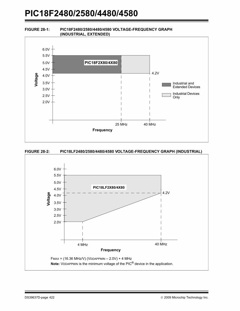
PIC18F2480/2580/4480/4580
FIGURE 28-1: PIC18F2480/2580/4480/4580 VOLTAGE-FREQUENCY GRAPH(INDUSTRIAL, EXTENDED)
FIGURE 28-2: PIC18LF2480/2580/4480/4580 VOLTAGE-FREQUENCY GRAPH (INDUSTRIAL)
Frequency
Volta
ge
6.0V
5.5V
4.5V
4.0V
2.0V
40 MHz
5.0V
3.5V
3.0V
2.5V
PIC18F2X80/4X80
4.2V
25 MHz
Industrial andExtended Devices
Industrial DevicesOnly
Frequency
Volta
ge
6.0V
5.5V
4.5V
4.0V
2.0V
40 MHz
5.0V
3.5V
3.0V
2.5V
PIC18LF2X80/4X80
FMAX = (16.36 MHz/V) (VDDAPPMIN – 2.0V) + 4 MHzNote: VDDAPPMIN is the minimum voltage of the PIC® device in the application.
4 MHz
4.2V
DS39637D-page 422 © 2009 Microchip Technology Inc.

PIC18F2480/2580/4480/4580
28.1 DC Characteristics: Supply VoltagePIC18F2480/2580/4480/4580 (Industrial, Extended) PIC18LF2480/2580/4480/4580 (Industrial)
PIC18LF2480/2580/4480/4580 (Industrial)
Standard Operating Conditions (unless otherwise stated)Operating temperature -40°C ≤ TA ≤ +85°C for industrial
PIC18F2480/2580/4480/4580 (Industrial, Extended)
Standard Operating Conditions (unless otherwise stated)Operating temperature -40°C ≤ TA ≤ +85°C for industrial
-40°C ≤ TA ≤ +125°C for extended
Param No. Symbol Characteristic Min Typ Max Units Conditions
VDD Supply VoltageD001 PIC18LF2X80/4X80 2.0 — 5.5 V
PIC18F2X80/4X80 4.2 — 5.5 VD001C AVDD Analog Supply Voltage VDD – 0.3 — VDD + 0.3 VD001D AVSS Analog Ground Voltage VSS – 0.3 — VSS + 0.3 VD002 VDR RAM Data Retention
Voltage(1)1.5 — — V
D003 VPOR VDD Start Voltage to ensure Internal Power-on Reset Signal
— — 0.7 V See section on Power-on Reset for details
D004 SVDD VDD Rise Rateto ensure Internal Power-on Reset Signal
0.05 — — V/ms See section on Power-on Reset for details
VBOR Brown-out Reset VoltageD005 PIC18LF2X80/4X80
BORV<1:0> = 11 2.00 2.1 2.16 VBORV<1:0> = 10 2.65 2.79 2.93 V
D005 All DevicesBORV<1:0> = 01(2) 4.11 4.33 4.55 VBORV<1:0> = 00 4.36 4.59 4.82 V
Legend: Shading of rows is to assist in readability of the table.Note 1: This is the limit to which VDD can be lowered in Sleep mode, or during a device Reset, without losing RAM data.
2: With BOR enabled, full-speed operation (FOSC = 40 MHz) is supported until a BOR occurs. This is valid although VDD may be below the minimum voltage for this frequency.
© 2009 Microchip Technology Inc. DS39637D-page 423
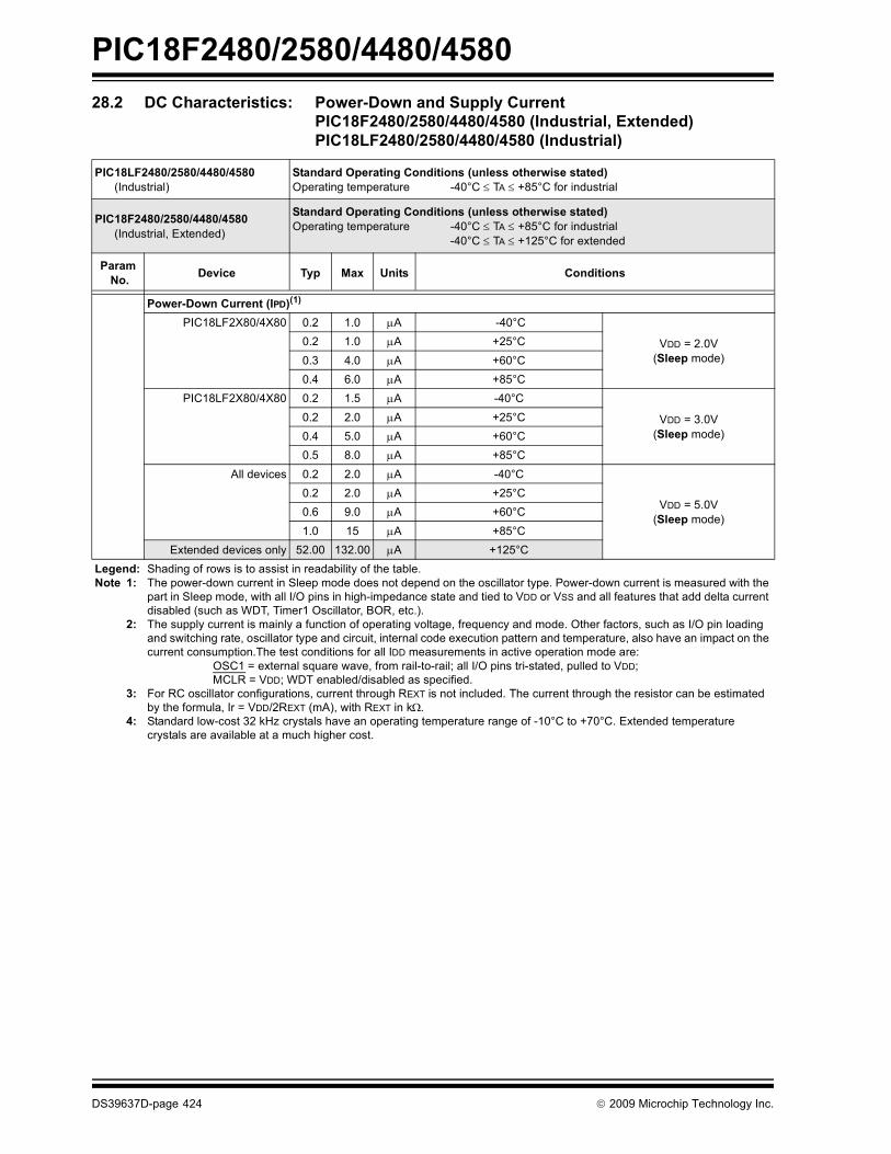
PIC18F2480/2580/4480/4580
28.2 DC Characteristics: Power-Down and Supply CurrentPIC18F2480/2580/4480/4580 (Industrial, Extended) PIC18LF2480/2580/4480/4580 (Industrial)
PIC18LF2480/2580/4480/4580 (Industrial)
Standard Operating Conditions (unless otherwise stated)Operating temperature -40°C ≤ TA ≤ +85°C for industrial
PIC18F2480/2580/4480/4580 (Industrial, Extended)
Standard Operating Conditions (unless otherwise stated)Operating temperature -40°C ≤ TA ≤ +85°C for industrial
-40°C ≤ TA ≤ +125°C for extended
Param No. Device Typ Max Units Conditions
Power-Down Current (IPD)(1)
PIC18LF2X80/4X80 0.2 1.0 μA -40°C
VDD = 2.0V(Sleep mode)
0.2 1.0 μA +25°C0.3 4.0 μA +60°C0.4 6.0 μA +85°C
PIC18LF2X80/4X80 0.2 1.5 μA -40°C
VDD = 3.0V(Sleep mode)
0.2 2.0 μA +25°C0.4 5.0 μA +60°C0.5 8.0 μA +85°C
All devices 0.2 2.0 μA -40°C
VDD = 5.0V(Sleep mode)
0.2 2.0 μA +25°C0.6 9.0 μA +60°C1.0 15 μA +85°C
Extended devices only 52.00 132.00 μA +125°CLegend: Shading of rows is to assist in readability of the table.Note 1: The power-down current in Sleep mode does not depend on the oscillator type. Power-down current is measured with the
part in Sleep mode, with all I/O pins in high-impedance state and tied to VDD or VSS and all features that add delta current disabled (such as WDT, Timer1 Oscillator, BOR, etc.).
2: The supply current is mainly a function of operating voltage, frequency and mode. Other factors, such as I/O pin loading and switching rate, oscillator type and circuit, internal code execution pattern and temperature, also have an impact on the current consumption.The test conditions for all IDD measurements in active operation mode are:
OSC1 = external square wave, from rail-to-rail; all I/O pins tri-stated, pulled to VDD;MCLR = VDD; WDT enabled/disabled as specified.
3: For RC oscillator configurations, current through REXT is not included. The current through the resistor can be estimated by the formula, Ir = VDD/2REXT (mA), with REXT in kΩ.
4: Standard low-cost 32 kHz crystals have an operating temperature range of -10°C to +70°C. Extended temperature crystals are available at a much higher cost.
DS39637D-page 424 © 2009 Microchip Technology Inc.

PIC18F2480/2580/4480/4580
Supply Current (IDD)(2,3)
PIC18LF2X80/4X80 19 31 μA -40°CVDD = 2.0V
FOSC = 31 kHz(RC_RUN mode,
Internal oscillator source)
21 31 μA +25°C22 31 μA +85°C
PIC18LF2X80/4X80 57 60 μA -40°CVDD = 3.0V47 60 μA +25°C
42 60 μA +85°CAll devices 150 170 μA -40°C
VDD = 5.0V113 170 μA +25°C98 170 μA +85°C
Extended devices only 170 280 μA +125°CPIC18LF2X80/4X80 530 1030 μA -40°C
VDD = 2.0V
FOSC = 1 MHz(RC_RUN mode,
Internal oscillator source)
550 1030 μA +25°C560 1030 μA +85°C
PIC18LF2X80/4X80 940 1150 μA -40°CVDD = 3.0V900 1150 μA +25°C
880.0 1150 μA +85°CAll devices 1.8 2.3 mA -40°C
VDD = 5.0V1.7 2.3 mA +25°C1.7 2.3 mA +85°C
Extended devices only 2.6 3.6 mA +125°C
28.2 DC Characteristics: Power-Down and Supply CurrentPIC18F2480/2580/4480/4580 (Industrial, Extended) PIC18LF2480/2580/4480/4580 (Industrial) (Continued)
PIC18LF2480/2580/4480/4580 (Industrial)
Standard Operating Conditions (unless otherwise stated)Operating temperature -40°C ≤ TA ≤ +85°C for industrial
PIC18F2480/2580/4480/4580 (Industrial, Extended)
Standard Operating Conditions (unless otherwise stated)Operating temperature -40°C ≤ TA ≤ +85°C for industrial
-40°C ≤ TA ≤ +125°C for extended
Param No. Device Typ Max Units Conditions
Legend: Shading of rows is to assist in readability of the table.Note 1: The power-down current in Sleep mode does not depend on the oscillator type. Power-down current is measured with the
part in Sleep mode, with all I/O pins in high-impedance state and tied to VDD or VSS and all features that add delta current disabled (such as WDT, Timer1 Oscillator, BOR, etc.).
2: The supply current is mainly a function of operating voltage, frequency and mode. Other factors, such as I/O pin loading and switching rate, oscillator type and circuit, internal code execution pattern and temperature, also have an impact on the current consumption.The test conditions for all IDD measurements in active operation mode are:
OSC1 = external square wave, from rail-to-rail; all I/O pins tri-stated, pulled to VDD;MCLR = VDD; WDT enabled/disabled as specified.
3: For RC oscillator configurations, current through REXT is not included. The current through the resistor can be estimated by the formula, Ir = VDD/2REXT (mA), with REXT in kΩ.
4: Standard low-cost 32 kHz crystals have an operating temperature range of -10°C to +70°C. Extended temperature crystals are available at a much higher cost.
© 2009 Microchip Technology Inc. DS39637D-page 425

PIC18F2480/2580/4480/4580
Supply Current (IDD)(2,3)
PIC18LF2X80/4X80 1.5 2.1 mA -40°CVDD = 2.0V
FOSC = 4 MHz(RC_RUN mode,
Internal oscillator source)
1.5 2.1 mA +25°C1.5 2.1 mA +85°C
PIC18LF2X80/4X80 2.4 3.3 mA -40°CVDD = 3.0V2.4 3.3 mA +25°C
2.4 3.3 mA +85°CAll devices 4.4 5.3 mA -40°C
VDD = 5.0V4.4 5.3 mA +25°C4.4 5.3 mA +85°C
Extended devices only 9.2 11 mA +125°CPIC18LF2X80/4X80 6.1 8.4 μA -40°C
VDD = 2.0V
FOSC = 31 kHz(RC_IDLE mode,
Internal oscillator source)
6.7 8.4 μA +25°C7.4 21 μA +85°C
PIC18LF2X80/4X80 9.6 12 μA -40°CVDD = 3.0V11 12 μA +25°C
12 33 μA +85°CAll devices 20 28 μA -40°C
VDD = 5.0V22 28 μA +25°C24 55 μA +85°C
Extended devices only 84 200 μA +125°C
28.2 DC Characteristics: Power-Down and Supply CurrentPIC18F2480/2580/4480/4580 (Industrial, Extended) PIC18LF2480/2580/4480/4580 (Industrial) (Continued)
PIC18LF2480/2580/4480/4580 (Industrial)
Standard Operating Conditions (unless otherwise stated)Operating temperature -40°C ≤ TA ≤ +85°C for industrial
PIC18F2480/2580/4480/4580 (Industrial, Extended)
Standard Operating Conditions (unless otherwise stated)Operating temperature -40°C ≤ TA ≤ +85°C for industrial
-40°C ≤ TA ≤ +125°C for extended
Param No. Device Typ Max Units Conditions
Legend: Shading of rows is to assist in readability of the table.Note 1: The power-down current in Sleep mode does not depend on the oscillator type. Power-down current is measured with the
part in Sleep mode, with all I/O pins in high-impedance state and tied to VDD or VSS and all features that add delta current disabled (such as WDT, Timer1 Oscillator, BOR, etc.).
2: The supply current is mainly a function of operating voltage, frequency and mode. Other factors, such as I/O pin loading and switching rate, oscillator type and circuit, internal code execution pattern and temperature, also have an impact on the current consumption.The test conditions for all IDD measurements in active operation mode are:
OSC1 = external square wave, from rail-to-rail; all I/O pins tri-stated, pulled to VDD;MCLR = VDD; WDT enabled/disabled as specified.
3: For RC oscillator configurations, current through REXT is not included. The current through the resistor can be estimated by the formula, Ir = VDD/2REXT (mA), with REXT in kΩ.
4: Standard low-cost 32 kHz crystals have an operating temperature range of -10°C to +70°C. Extended temperature crystals are available at a much higher cost.
DS39637D-page 426 © 2009 Microchip Technology Inc.

PIC18F2480/2580/4480/4580
Supply Current (IDD)(2,3)
PIC18LF2X80/4X80 300 390 μA -40°CVDD = 2.0V
FOSC = 1 MHz(RC_IDLE mode,
Internal oscillator source)
320 390 μA +25°C330 390 μA +85°C
PIC18LF2X80/4X80 450 550 μA -40°CVDD = 3.0V470 550 μA +25°C
490 550 μA +85°CAll devices 840 1030 μA -40°C
VDD = 5.0V880 1030 μA +25°C900 1030 μA +85°C
Extended devices only 2.8 3.2 mA +125°CPIC18LF2X80/4X80 760 1050 μA -40°C
VDD = 2.0V
FOSC = 4 MHz(RC_IDLE mode,
Internal oscillator source)
790 1050 μA +25°C810 1050 μA +85°C
PIC18LF2X80/4X80 1.2 1.5 mA -40°CVDD = 3.0V1.2 1.5 mA +25°C
1.3 1.5 mA +85°CAll devices 2.2 2.7 mA -40°C
VDD = 5.0V2.3 2.7 mA +25°C2.3 2.7 mA +85°C
Extended devices only 4.7 5.5 mA +125°CPIC18LF2X80/4X80 410 550 μA -40°C
VDD = 2.0V
FOSC = 1 MHZ(PRI_RUN,
EC oscillator)
420 550 μA +25°C420 550 μA +85°C
PIC18LF2X80/4X80 870 830 μA -40°CVDD = 3.0V770 830 μA +25°C
720 830 μA +85°CAll devices 1.8 3.3 mA -40°C
VDD = 5.0V1.6 3.3 mA +25°C1.5 3.3 mA +85°C
Extended devices only 1.5 3.3 mA +125°C
28.2 DC Characteristics: Power-Down and Supply CurrentPIC18F2480/2580/4480/4580 (Industrial, Extended) PIC18LF2480/2580/4480/4580 (Industrial) (Continued)
PIC18LF2480/2580/4480/4580 (Industrial)
Standard Operating Conditions (unless otherwise stated)Operating temperature -40°C ≤ TA ≤ +85°C for industrial
PIC18F2480/2580/4480/4580 (Industrial, Extended)
Standard Operating Conditions (unless otherwise stated)Operating temperature -40°C ≤ TA ≤ +85°C for industrial
-40°C ≤ TA ≤ +125°C for extended
Param No. Device Typ Max Units Conditions
Legend: Shading of rows is to assist in readability of the table.Note 1: The power-down current in Sleep mode does not depend on the oscillator type. Power-down current is measured with the
part in Sleep mode, with all I/O pins in high-impedance state and tied to VDD or VSS and all features that add delta current disabled (such as WDT, Timer1 Oscillator, BOR, etc.).
2: The supply current is mainly a function of operating voltage, frequency and mode. Other factors, such as I/O pin loading and switching rate, oscillator type and circuit, internal code execution pattern and temperature, also have an impact on the current consumption.The test conditions for all IDD measurements in active operation mode are:
OSC1 = external square wave, from rail-to-rail; all I/O pins tri-stated, pulled to VDD;MCLR = VDD; WDT enabled/disabled as specified.
3: For RC oscillator configurations, current through REXT is not included. The current through the resistor can be estimated by the formula, Ir = VDD/2REXT (mA), with REXT in kΩ.
4: Standard low-cost 32 kHz crystals have an operating temperature range of -10°C to +70°C. Extended temperature crystals are available at a much higher cost.
© 2009 Microchip Technology Inc. DS39637D-page 427

PIC18F2480/2580/4480/4580
Supply Current (IDD)(2,3)
PIC18LF2X80/4X80 1.4 2.2 mA -40°CVDD = 2.0V
FOSC = 4 MHz(PRI_RUN,
EC oscillator)
1.4 2.2 mA +25°C1.4 2.2 mA +85°C
PIC18LF2X80/4X80 2.3 3.3 mA -40°CVDD = 3.0V2.3 3.3 mA +25°C
2.3 3.3 mA +85°CAll devices 4.5 6.6 mA -40°C
VDD = 5.0V4.3 6.6 mA +25°C4.3 6.6 mA +85°C
Extended devices only 5 7.7 mA +125°C15 23 mA +125°C VDD = 4.2V FOSC = 25 MHz
(PRI_RUN,EC oscillator)
20 31 mA +125°CVDD = 5.0V
All devices 30 38 mA -40°CVDD = 4.2V
FOSC = 40 MHZ(PRI_RUN,
EC oscillator)
31 38 mA +25°C31 38 mA +85°C
All devices 37 44 mA -40°CVDD = 5.0V38 44 mA +25°C
39 44 mA +85°C
28.2 DC Characteristics: Power-Down and Supply CurrentPIC18F2480/2580/4480/4580 (Industrial, Extended) PIC18LF2480/2580/4480/4580 (Industrial) (Continued)
PIC18LF2480/2580/4480/4580 (Industrial)
Standard Operating Conditions (unless otherwise stated)Operating temperature -40°C ≤ TA ≤ +85°C for industrial
PIC18F2480/2580/4480/4580 (Industrial, Extended)
Standard Operating Conditions (unless otherwise stated)Operating temperature -40°C ≤ TA ≤ +85°C for industrial
-40°C ≤ TA ≤ +125°C for extended
Param No. Device Typ Max Units Conditions
Legend: Shading of rows is to assist in readability of the table.Note 1: The power-down current in Sleep mode does not depend on the oscillator type. Power-down current is measured with the
part in Sleep mode, with all I/O pins in high-impedance state and tied to VDD or VSS and all features that add delta current disabled (such as WDT, Timer1 Oscillator, BOR, etc.).
2: The supply current is mainly a function of operating voltage, frequency and mode. Other factors, such as I/O pin loading and switching rate, oscillator type and circuit, internal code execution pattern and temperature, also have an impact on the current consumption.The test conditions for all IDD measurements in active operation mode are:
OSC1 = external square wave, from rail-to-rail; all I/O pins tri-stated, pulled to VDD;MCLR = VDD; WDT enabled/disabled as specified.
3: For RC oscillator configurations, current through REXT is not included. The current through the resistor can be estimated by the formula, Ir = VDD/2REXT (mA), with REXT in kΩ.
4: Standard low-cost 32 kHz crystals have an operating temperature range of -10°C to +70°C. Extended temperature crystals are available at a much higher cost.
DS39637D-page 428 © 2009 Microchip Technology Inc.

PIC18F2480/2580/4480/4580
Supply Current (IDD)(2,3)
PIC18LF2X80/4X80 160 220 μA -40°CVDD = 2.0V
FOSC = 1 MHz(PRI_IDLE mode,
EC oscillator)
170 220 μA +25°C170 220 μA +85°C
PIC18LF2X80/4X80 250 330 μA -40°CVDD = 3.0V260 330 μA +25°C
260 330 μA +85°CAll devices 460 550 μA -40°C
VDD = 5.0V470 550 μA +25°C480 550 μA +85°C
Extended devices only 790 920 μA +125°CPIC18LF2X80/4X80 640 715 μA -40°C
VDD = 2.0V
FOSC = 4 MHz(PRI_IDLE mode,
EC oscillator)
650 715 μA +25°C660 715 μA +85°C
PIC18LF2X80/4X80 0.98 1.4 mA -40°CVDD = 3.0V1 1.4 mA +25°C
1.1 1.4 mA +85°CAll devices 1.9 2.2 mA -40°C
VDD = 5.0V1.9 2.2 mA +25°C1.9 2.2 mA +85°C
Extended devices only 2.1 2.4 mA +125°C9.5 11 mA +125°C VDD = 4.2V FOSC = 25 MHz
(PRI_IDLE mode, EC oscillator)
14 16 mA +125°CVDD = 5.0V
All devices 15 18 mA -40°CVDD = 4.2 V
FOSC = 40 MHz(PRI_IDLE mode,
EC oscillator)
16 18 mA +25°C16 18 mA +85°C
All devices 19 22 mA -40°CVDD = 5.0V19 22 mA +25°C
20 22 mA +85°C
28.2 DC Characteristics: Power-Down and Supply CurrentPIC18F2480/2580/4480/4580 (Industrial, Extended) PIC18LF2480/2580/4480/4580 (Industrial) (Continued)
PIC18LF2480/2580/4480/4580 (Industrial)
Standard Operating Conditions (unless otherwise stated)Operating temperature -40°C ≤ TA ≤ +85°C for industrial
PIC18F2480/2580/4480/4580 (Industrial, Extended)
Standard Operating Conditions (unless otherwise stated)Operating temperature -40°C ≤ TA ≤ +85°C for industrial
-40°C ≤ TA ≤ +125°C for extended
Param No. Device Typ Max Units Conditions
Legend: Shading of rows is to assist in readability of the table.Note 1: The power-down current in Sleep mode does not depend on the oscillator type. Power-down current is measured with the
part in Sleep mode, with all I/O pins in high-impedance state and tied to VDD or VSS and all features that add delta current disabled (such as WDT, Timer1 Oscillator, BOR, etc.).
2: The supply current is mainly a function of operating voltage, frequency and mode. Other factors, such as I/O pin loading and switching rate, oscillator type and circuit, internal code execution pattern and temperature, also have an impact on the current consumption.The test conditions for all IDD measurements in active operation mode are:
OSC1 = external square wave, from rail-to-rail; all I/O pins tri-stated, pulled to VDD;MCLR = VDD; WDT enabled/disabled as specified.
3: For RC oscillator configurations, current through REXT is not included. The current through the resistor can be estimated by the formula, Ir = VDD/2REXT (mA), with REXT in kΩ.
4: Standard low-cost 32 kHz crystals have an operating temperature range of -10°C to +70°C. Extended temperature crystals are available at a much higher cost.
© 2009 Microchip Technology Inc. DS39637D-page 429

PIC18F2480/2580/4480/4580
Supply Current (IDD)(2,3)
PIC18LF2X80/4X80 19 44 μA -40°CVDD = 2.0V
FOSC = 32 kHz(SEC_RUN mode, Timer1 as clock)(4)
20 44 μA +25°C 22 44 μA +85°C
PIC18LF2X80/4X80 56 71 μA -40°CVDD = 3.0V45 71 μA +25°C
41 71 μA +85°CAll devices 140 165 μA -40°C
VDD = 5.0V106 165 μA +25°C 95 165 μA +85°C
PIC18LF2X80/4X80 6.1 13 μA -40°CVDD = 2.0V
FOSC = 32 kHz(SEC_IDLE mode, Timer1 as clock)(4)
6.6 13 μA +25°C 7.7 13 μA +85°C
PIC18LF2X80/4X80 9.3 33 μA -40°CVDD = 3.0V9.4 33 μA +25°C
11 33 μA +85°CAll devices 17 50 μA -40°C
VDD = 5.0V17 50 μA +25°C 20 50 μA +85°C
28.2 DC Characteristics: Power-Down and Supply CurrentPIC18F2480/2580/4480/4580 (Industrial, Extended) PIC18LF2480/2580/4480/4580 (Industrial) (Continued)
PIC18LF2480/2580/4480/4580 (Industrial)
Standard Operating Conditions (unless otherwise stated)Operating temperature -40°C ≤ TA ≤ +85°C for industrial
PIC18F2480/2580/4480/4580 (Industrial, Extended)
Standard Operating Conditions (unless otherwise stated)Operating temperature -40°C ≤ TA ≤ +85°C for industrial
-40°C ≤ TA ≤ +125°C for extended
Param No. Device Typ Max Units Conditions
Legend: Shading of rows is to assist in readability of the table.Note 1: The power-down current in Sleep mode does not depend on the oscillator type. Power-down current is measured with the
part in Sleep mode, with all I/O pins in high-impedance state and tied to VDD or VSS and all features that add delta current disabled (such as WDT, Timer1 Oscillator, BOR, etc.).
2: The supply current is mainly a function of operating voltage, frequency and mode. Other factors, such as I/O pin loading and switching rate, oscillator type and circuit, internal code execution pattern and temperature, also have an impact on the current consumption.The test conditions for all IDD measurements in active operation mode are:
OSC1 = external square wave, from rail-to-rail; all I/O pins tri-stated, pulled to VDD;MCLR = VDD; WDT enabled/disabled as specified.
3: For RC oscillator configurations, current through REXT is not included. The current through the resistor can be estimated by the formula, Ir = VDD/2REXT (mA), with REXT in kΩ.
4: Standard low-cost 32 kHz crystals have an operating temperature range of -10°C to +70°C. Extended temperature crystals are available at a much higher cost.
DS39637D-page 430 © 2009 Microchip Technology Inc.

PIC18F2480/2580/4480/4580
Module Differential Currents (ΔIWDT, ΔIBOR, ΔILVD, ΔIOSCB, ΔIAD)D022(ΔIWDT)
Watchdog Timer 1.7 7.6 μA -40°CVDD = 2.0V2.1 8 μA +25°C
2.6 8.4 μA +85°C2.2 11.4 μA -40°C
VDD = 3.0V2.4 12 μA +25°C2.8 12.6 μA +85°C2.9 14.3 μA -40°C
VDD = 5.0V3.1 15 μA +25°C3.3 15.8 μA +85°C
7.80 19 μA +125°C
D022A(ΔIBOR)
Brown-out Reset 17 75 μA -40°C to +85°C VDD = 3.0V47 92 μA -40°C to +85°C
VDD = 5.0V30 58 μA +125°C0 2 μA -40°C to +85°C Sleep mode0 5 μA -40°C to +125°C BOREN<1:0>
D022B High/Low-Voltage Detect 14 47 μA -40°C to +85°C VDD = 2.0V
(ΔILVD) 18 58 μA -40°C to +85°C VDD = 3.0V21 69 μA -40°C to +85°C
VDD = 5.0V19 50 μA +125°C
D025 Timer1 Oscillator 1.0 8 μA -40°CVDD = 2.0V 32 kHz on Timer1(4)(ΔIOSCB) 1.1 8 μA +25°C
1.1 8 μA +85°C1.2 8.2 μA -40°C
VDD = 3.0V 32 kHz on Timer1(4)1.3 8.2 μA +25°C1.2 8.2 μA +85°C1.8 10 μA -40°C
VDD = 5.0V 32 kHz on Timer1(4)1.9 10 μA +25°C1.9 10 μA +85°C
28.2 DC Characteristics: Power-Down and Supply CurrentPIC18F2480/2580/4480/4580 (Industrial, Extended) PIC18LF2480/2580/4480/4580 (Industrial) (Continued)
PIC18LF2480/2580/4480/4580 (Industrial)
Standard Operating Conditions (unless otherwise stated)Operating temperature -40°C ≤ TA ≤ +85°C for industrial
PIC18F2480/2580/4480/4580 (Industrial, Extended)
Standard Operating Conditions (unless otherwise stated)Operating temperature -40°C ≤ TA ≤ +85°C for industrial
-40°C ≤ TA ≤ +125°C for extended
Param No. Device Typ Max Units Conditions
Legend: Shading of rows is to assist in readability of the table.Note 1: The power-down current in Sleep mode does not depend on the oscillator type. Power-down current is measured with the
part in Sleep mode, with all I/O pins in high-impedance state and tied to VDD or VSS and all features that add delta current disabled (such as WDT, Timer1 Oscillator, BOR, etc.).
2: The supply current is mainly a function of operating voltage, frequency and mode. Other factors, such as I/O pin loading and switching rate, oscillator type and circuit, internal code execution pattern and temperature, also have an impact on the current consumption.The test conditions for all IDD measurements in active operation mode are:
OSC1 = external square wave, from rail-to-rail; all I/O pins tri-stated, pulled to VDD;MCLR = VDD; WDT enabled/disabled as specified.
3: For RC oscillator configurations, current through REXT is not included. The current through the resistor can be estimated by the formula, Ir = VDD/2REXT (mA), with REXT in kΩ.
4: Standard low-cost 32 kHz crystals have an operating temperature range of -10°C to +70°C. Extended temperature crystals are available at a much higher cost.
© 2009 Microchip Technology Inc. DS39637D-page 431

PIC18F2480/2580/4480/4580
D026(ΔIAD)
A/D Converter 1.0 2.0 μA -40°C to +85°C VDD = 2.0V
A/D on, not converting1.0 2.0 μA -40°C to +85°C VDD = 3.0V
1.0 2.0 μA -40°C to +85°CVDD = 5.0V
2.0 8.0 μA -40°C to +125°C
28.2 DC Characteristics: Power-Down and Supply CurrentPIC18F2480/2580/4480/4580 (Industrial, Extended) PIC18LF2480/2580/4480/4580 (Industrial) (Continued)
PIC18LF2480/2580/4480/4580 (Industrial)
Standard Operating Conditions (unless otherwise stated)Operating temperature -40°C ≤ TA ≤ +85°C for industrial
PIC18F2480/2580/4480/4580 (Industrial, Extended)
Standard Operating Conditions (unless otherwise stated)Operating temperature -40°C ≤ TA ≤ +85°C for industrial
-40°C ≤ TA ≤ +125°C for extended
Param No. Device Typ Max Units Conditions
Legend: Shading of rows is to assist in readability of the table.Note 1: The power-down current in Sleep mode does not depend on the oscillator type. Power-down current is measured with the
part in Sleep mode, with all I/O pins in high-impedance state and tied to VDD or VSS and all features that add delta current disabled (such as WDT, Timer1 Oscillator, BOR, etc.).
2: The supply current is mainly a function of operating voltage, frequency and mode. Other factors, such as I/O pin loading and switching rate, oscillator type and circuit, internal code execution pattern and temperature, also have an impact on the current consumption.The test conditions for all IDD measurements in active operation mode are:
OSC1 = external square wave, from rail-to-rail; all I/O pins tri-stated, pulled to VDD;MCLR = VDD; WDT enabled/disabled as specified.
3: For RC oscillator configurations, current through REXT is not included. The current through the resistor can be estimated by the formula, Ir = VDD/2REXT (mA), with REXT in kΩ.
4: Standard low-cost 32 kHz crystals have an operating temperature range of -10°C to +70°C. Extended temperature crystals are available at a much higher cost.
DS39637D-page 432 © 2009 Microchip Technology Inc.
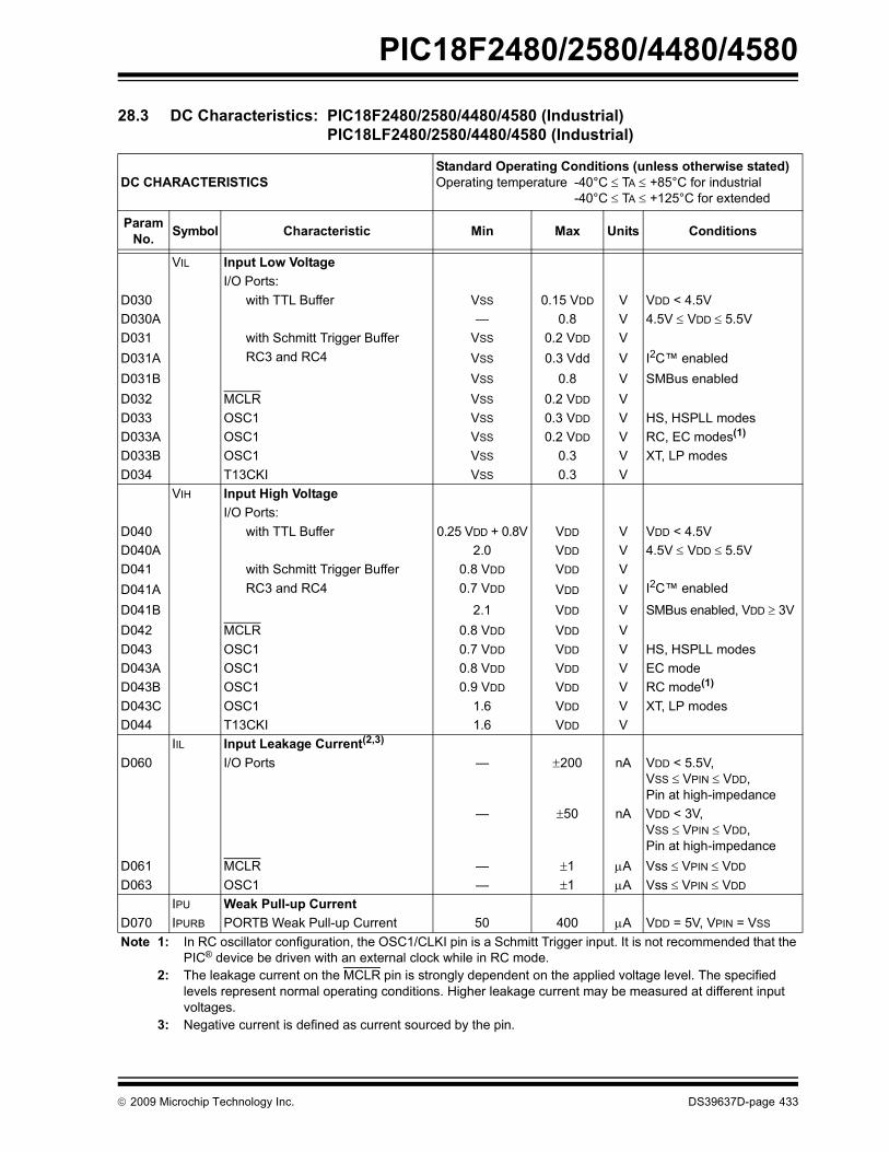
PIC18F2480/2580/4480/4580
28.3 DC Characteristics: PIC18F2480/2580/4480/4580 (Industrial) PIC18LF2480/2580/4480/4580 (Industrial)
DC CHARACTERISTICSStandard Operating Conditions (unless otherwise stated)Operating temperature -40°C ≤ TA ≤ +85°C for industrial
-40°C ≤ TA ≤ +125°C for extended
ParamNo. Symbol Characteristic Min Max Units Conditions
VIL Input Low VoltageI/O Ports:
D030 with TTL Buffer VSS 0.15 VDD V VDD < 4.5V D030A — 0.8 V 4.5V ≤ VDD ≤ 5.5V D031 with Schmitt Trigger Buffer VSS 0.2 VDD VD031A RC3 and RC4 VSS 0.3 Vdd V I2C™ enabledD031B VSS 0.8 V SMBus enabledD032 MCLR VSS 0.2 VDD VD033 OSC1 VSS 0.3 VDD V HS, HSPLL modesD033A OSC1 VSS 0.2 VDD V RC, EC modes(1)
D033B OSC1 VSS 0.3 V XT, LP modesD034 T13CKI VSS 0.3 V
VIH Input High VoltageI/O Ports:
D040 with TTL Buffer 0.25 VDD + 0.8V VDD V VDD < 4.5VD040A 2.0 VDD V 4.5V ≤ VDD ≤ 5.5V D041 with Schmitt Trigger Buffer 0.8 VDD VDD VD041A RC3 and RC4 0.7 VDD VDD V I2C™ enabled
D041B 2.1 VDD V SMBus enabled, VDD ≥ 3VD042 MCLR 0.8 VDD VDD VD043 OSC1 0.7 VDD VDD V HS, HSPLL modesD043A OSC1 0.8 VDD VDD V EC modeD043B OSC1 0.9 VDD VDD V RC mode(1)
D043C OSC1 1.6 VDD V XT, LP modesD044 T13CKI 1.6 VDD V
IIL Input Leakage Current(2,3) D060 I/O Ports — ±200 nA VDD < 5.5V,
VSS ≤ VPIN ≤ VDD, Pin at high-impedance
— ±50 nA VDD < 3V,VSS ≤ VPIN ≤ VDD, Pin at high-impedance
D061 MCLR — ±1 μA Vss ≤ VPIN ≤ VDD
D063 OSC1 — ±1 μA Vss ≤ VPIN ≤ VDD IPU Weak Pull-up Current
D070 IPURB PORTB Weak Pull-up Current 50 400 μA VDD = 5V, VPIN = VSS
Note 1: In RC oscillator configuration, the OSC1/CLKI pin is a Schmitt Trigger input. It is not recommended that the PIC® device be driven with an external clock while in RC mode.
2: The leakage current on the MCLR pin is strongly dependent on the applied voltage level. The specified levels represent normal operating conditions. Higher leakage current may be measured at different input voltages.
3: Negative current is defined as current sourced by the pin.
© 2009 Microchip Technology Inc. DS39637D-page 433

PIC18F2480/2580/4480/4580
VOL Output Low VoltageD080 I/O Ports — 0.6 V IOL = 8.5 mA, VDD = 4.5V,
-40°C to +85°CD083 OSC2/CLKO
(RC, RCIO, EC, ECIO modes)— 0.6 V IOL = 1.6 mA, VDD = 4.5V,
-40°C to +85°CVOH Output High Voltage(3)
D090 I/O Ports VDD – 0.7 — V IOH = -3.0 mA, VDD = 4.5V,-40°C to +85°C
D092 OSC2/CLKO (RC, RCIO, EC, ECIO modes)
VDD – 0.7 — V IOH = -1.3 mA, VDD = 4.5V,-40°C to +85°C
Capacitive Loading Specson Output Pins
D100 COSC2 OSC2 Pin — 15 pF In XT, HS and LP modes when external clock is used to drive OSC1
D101 CIO All I/O Pins and OSC2 (in RC mode)
— 50 pF To meet the AC Timing Specifications
D102 CB SCL, SDA — 400 pF I2C™ Specification
28.3 DC Characteristics: PIC18F2480/2580/4480/4580 (Industrial) PIC18LF2480/2580/4480/4580 (Industrial) (Continued)
DC CHARACTERISTICSStandard Operating Conditions (unless otherwise stated)Operating temperature -40°C ≤ TA ≤ +85°C for industrial
-40°C ≤ TA ≤ +125°C for extended
ParamNo. Symbol Characteristic Min Max Units Conditions
Note 1: In RC oscillator configuration, the OSC1/CLKI pin is a Schmitt Trigger input. It is not recommended that the PIC® device be driven with an external clock while in RC mode.
2: The leakage current on the MCLR pin is strongly dependent on the applied voltage level. The specified levels represent normal operating conditions. Higher leakage current may be measured at different input voltages.
3: Negative current is defined as current sourced by the pin.
DS39637D-page 434 © 2009 Microchip Technology Inc.

PIC18F2480/2580/4480/4580
TABLE 28-1: MEMORY PROGRAMMING REQUIREMENTSDC CharacteristicsStandard Operating Conditions (unless otherwise stated)Operating temperature -40°C ≤ TA ≤ +85°C for industrial
-40°C ≤ TA ≤ +125°C for extended
ParamNo. Sym Characteristic Min Typ† Max Units Conditions
Internal Program Memory Programming Specifications(1)
D110 VPP Voltage on MCLR/VPP/RE3 Pin 9.00 — 13.25 V (Note 3)D113 IDDP Supply Current during
Programming— — 10 mA
Data EEPROM MemoryD120 ED Byte Endurance 100K 1M — E/W -40°C to +85°CD121 VDRW VDD for Read/Write VMIN — 5.5 V Using EECON to read/write
VMIN = Minimum operating voltage
D122 TDEW Erase/Write Cycle Time — 4 — msD123 TRETD Characteristic Retention 40 — — Year Provided no other
specifications are violatedD124 TREF Number of Total Erase/Write
Cycles before Refresh(2)1M 10M — E/W -40°C to +85°C
Program Flash MemoryD130 EP Cell Endurance 10K 100K — E/W -40°C to +85°CD131 VPR VDD for Read VMIN — 5.5 V VMIN = Minimum operating
voltageD132 VIE VDD for Block Erase 4.5 — 5.5 V Using ICSP™ portD132A VIW VDD for Externally Timed Erase
or Write4.5 — 5.5 V Using ICSP port
D132B VPEW VDD for Self-Timed Write VMIN — 5.5 V VMIN = Minimum operating voltage
D133 TIE ICSP Block Erase Cycle Time — 4 — ms VDD > 4.5VD133A TIW ICSP Erase or Write Cycle Time
(externally timed)1 — — ms VDD > 4.5V
D133A TIW Self-Timed Write Cycle Time — 2 — msD134 TRETD Characteristic Retention 40 100 — Year Provided no other
specifications are violated† Data in “Typ” column is at 5.0V, 25°C unless otherwise stated. These parameters are for design guidance
only and are not tested.Note 1: These specifications are for programming the on-chip program memory through the use of table write
instructions.2: Refer to Section 8.8 “Using the Data EEPROM” for a more detailed discussion on data EEPROM
endurance.3: Required only if Single-Supply Programming is disabled.
© 2009 Microchip Technology Inc. DS39637D-page 435

PIC18F2480/2580/4480/4580
TABLE 28-2: COMPARATOR SPECIFICATIONSTABLE 28-3: VOLTAGE REFERENCE SPECIFICATIONS
Operating Conditions: 3.0V < VDD < 5.5V, -40°C < TA < +85°C (unless otherwise stated)-40°C < TA < +125°C for extended
ParamNo. Sym Characteristics Min Typ Max Units Comments
D300 VIOFF Input Offset Voltage — ±5.0 ±10 mVD301 VICM Input Common Mode Voltage 0 — VDD – 1.5 VD302 CMRR Common Mode Rejection Ratio 55 — — dBD303 TRESP Response Time(1)* — 150 400 ns PIC18FXXXXD303A — 150 600 ns PIC18LFXXXX,
VDD = 2.0VD304 TMC2OV Comparator Mode Change to
Output Valid*— — 10 μs
Note 1: Response time measured with one comparator input at (VDD – 1.5)/2 while the other input transitions from VSS to VDD.
Operating Conditions: 3.0V < VDD < 5.5V, -40°C < TA < +85°C (unless otherwise stated)-40°C < TA < +125°C for extended
ParamNo. Sym Characteristics Min Typ Max Units Comments
D310 VRES Resolution VDD/24 — VDD/32 LSbD311 VRAA Absolute Accuracy —
———
1/41/2
LSbLSb
Low Range (CVRR = 1)High Range (CVRR = 0)
D312 VRUR Unit Resistor Value (R) — 2k — Ω
D313 TSET Settling Time(1) — — 10 μs
Note 1: Settling time measured while CVRR = 1 and CVR<3:0> bits transition from ‘0000’ to ‘1111’.
DS39637D-page 436 © 2009 Microchip Technology Inc.

PIC18F2480/2580/4480/4580
FIGURE 28-3: HIGH/LOW-VOLTAGE DETECT CHARACTERISTICSTABLE 28-4: HIGH/LOW-VOLTAGE DETECT CHARACTERISTICS Standard Operating Conditions (unless otherwise stated)Operating temperature -40°C ≤ TA ≤ +85°C for industrial
-40°C < TA < +125°C for extended
Param No. Symbol Characteristic Min Typ Max Units Conditions
D420 HLVD Voltage on VDD Transition High-to-Low
LVV = 0000 2.12 2.17 2.22 VLVV = 0001 2.18 2.23 2.28 VLVV = 0010 2.31 2.36 2.42 VLVV = 0011 2.38 2.44 2.49 VLVV = 0100 2.54 2.60 2.66 VLVV = 0101 2.72 2.79 2.85 VLVV = 0110 2.82 2.89 2.95 VLVV = 0111 3.05 3.12 3.19 VLVV = 1000 3.31 3.39 3.47 VLVV = 1001 3.46 3.55 3.63 VLVV = 1010 3.63 3.71 3.80 VLVV = 1011 3.81 3.90 3.99 VLVV = 1100 4.01 4.11 4.20 VLVV = 1101 4.23 4.33 4.43 VLVV = 1110 4.48 4.59 4.69 VLVV = 1111 1.14 1.2 1.26 V
VLVD
HLVDIF
VDD
(HLVDIF set by hardware)
(HLVDIF can be cleared in software)
© 2009 Microchip Technology Inc. DS39637D-page 437

PIC18F2480/2580/4480/4580
28.4 AC (Timing) Characteristics28.4.1 TIMING PARAMETER SYMBOLOGYThe timing parameter symbols have been createdusing one of the following formats:
1. TppS2ppS 3. TCC:ST (I2C specifications only)2. TppS 4. Ts (I2C specifications only)T
F Frequency T TimeLowercase letters (pp) and their meanings:pp
cc CCP1 osc OSC1ck CLKO rd RDcs CS rw RD or WRdi SDI sc SCKdo SDO ss SSdt Data in t0 T0CKIio I/O port t1 T13CKImc MCLR wr WR
Uppercase letters and their meanings:S
F Fall P PeriodH High R RiseI Invalid (High-impedance) V ValidL Low Z High-impedance
I2C onlyAA output access High HighBUF Bus free Low Low
TCC:ST (I2C specifications only)CC
HD Hold SU SetupST
DAT DATA input hold STO Stop conditionSTA Start condition
DS39637D-page 438 © 2009 Microchip Technology Inc.

PIC18F2480/2580/4480/4580
28.4.2 TIMING CONDITIONSThe temperature and voltages specified in Table 28-5apply to all timing specifications unless otherwisenoted. Figure 28-4 specifies the load conditions for thetiming specifications.TABLE 28-5: TEMPERATURE AND VOLTAGE SPECIFICATIONS – AC
FIGURE 28-4: LOAD CONDITIONS FOR DEVICE TIMING SPECIFICATIONS
Note: Because of space limitations, the genericterms “PIC18FXXXX” and “PIC18LFXXXX”are used throughout this section to refer tothe PIC18F2480/2580/4480/4580 andPIC18LF2480/2580/4480/4580 families ofdevices specifically and only those devices.
AC CHARACTERISTICS
Standard Operating Conditions (unless otherwise stated)Operating temperature -40°C ≤ TA ≤ +85°C for industrial
-40°C < TA < +125°C for extendedOperating voltage VDD range as described in DC spec Section 28.1 and Section 28.3. LF parts operate for industrial temperatures only.
VDD/2
CL
RL
Pin
Pin
VSS
VSS
CL
RL = 464Ω
CL = 50 pF for all pins except OSC2/CLKOand including D and E outputs as ports
Load Condition 1 Load Condition 2
© 2009 Microchip Technology Inc. DS39637D-page 439

PIC18F2480/2580/4480/4580
28.4.3 TIMING DIAGRAMS AND SPECIFICATIONSFIGURE 28-5: EXTERNAL CLOCK TIMING (ALL MODES EXCEPT PLL)
TABLE 28-6: EXTERNAL CLOCK TIMING REQUIREMENTS Param.
No. Symbol Characteristic Min Max Units Conditions
1A FOSC External CLKI Frequency(1) DC 1 MHz XT, RC Oscillator modeDC 25 MHz HS Oscillator modeDC 31.25 kHz LP Oscillator modeDC 40 MHz EC Oscillator mode
Oscillator Frequency(1) DC 4 MHz RC Oscillator mode0.1 4 MHz XT Oscillator mode4 25 MHz HS Oscillator mode4 10 MHz HSPLL Oscillator mode5 200 kHz LP Oscillator mode
1 TOSC External CLKI Period(1) 1000 — ns XT, RC Oscillator mode40 — ns HS Oscillator mode32 — μs LP Oscillator mode25 — ns EC Oscillator mode
Oscillator Period(1) 250250
—1
nsμs
RC Oscillator modeXT Oscillator mode
40 250 ns HS Oscillator mode100 250 ns HSPLL Oscillator mode5 200 μs LP Oscillator mode
2 TCY Instruction Cycle Time(1) 100 — ns TCY = 4/FOSC, Industrial 160 — ns TCY = 4/FOSC, Extended
3 TOSL,TOSH
External Clock in (OSC1) High or Low Time
30 — ns XT Oscillator mode2.5 — μs LP Oscillator mode10 — ns HS Oscillator mode
4 TOSR,TOSF
External Clock in (OSC1) Rise or Fall Time
— 20 ns XT Oscillator mode— 50 ns LP Oscillator mode— 7.5 ns HS Oscillator mode
Note 1: Instruction cycle period (TCY) equals four times the input oscillator time base period for all configurations except PLL. All specified values are based on characterization data for that particular oscillator type under standard operating conditions with the device executing code. Exceeding these specified limits may result in an unstable oscillator operation and/or higher than expected current consumption. All devices are tested to operate at “min.” values with an external clock applied to the OSC1/CLKI pin. When an external clock input is used, the “max.” cycle time limit is “DC” (no clock) for all devices.
OSC1
CLKO
Q4 Q1 Q2 Q3 Q4 Q1
1
23 3 4 4
DS39637D-page 440 © 2009 Microchip Technology Inc.

PIC18F2480/2580/4480/4580
TABLE 28-7: PLL CLOCK TIMING SPECIFICATIONS (VDD = 4.2V TO 5.5V)TABLE 28-8: AC CHARACTERISTICS: INTERNAL RC ACCURACYPIC18F2480/2580/4480/4580 (INDUSTRIAL)PIC18LF2480/2580/4480/4580 (INDUSTRIAL)
Param No. Sym Characteristic Min Typ† Max Units Conditions
F10 FOSC Oscillator Frequency Range 4 — 10 MHz HS mode onlyF11 FSYS On-Chip VCO System Frequency 16 — 40 MHz HS mode onlyF12 trc PLL Start-up Time (lock time) — — 2 msF13 ΔCLK CLKO Stability (jitter) -2 — +2 %
† Data in “Typ” column is at 5V, 25°C unless otherwise stated. These parameters are for design guidance only and are not tested.
PIC18F2480/2580/4480/4580 (Industrial)
Standard Operating Conditions (unless otherwise stated)Operating temperature -40°C ≤ TA ≤ +85°C for industrial
-40°C < TA < +125°C for extended
ParamNo. Device Min Typ Max Units Conditions
INTOSC Accuracy @ Freq = 8 MHz, 4 MHz, 2 MHz, 1 MHz, 500 kHz, 250 kHz, 125 kHz(1)
PIC18LF2X80/4X80 -2 +/-1 2 % +25°C VDD = 2.7-3.3V-5 — 5 % -10°C to +85°C VDD = 2.7-3.3V
-10 +/-1 10 % -40°C to +85°C VDD = 2.7-3.3VPIC18F2X80/4X80 -2 +/-1 2 % +25°C VDD = 4.5-5.5V
-5 — 5 % -10°C to +85°C VDD = 4.5-5.5V-10 +/-1 10 % -40°C to +85°C VDD = 4.5-5.5V
INTRC Accuracy @ Freq = 31 kHzPIC18LF2X80/4X80 26.562 — 35.938 kHz -40°C to +85°C VDD = 2.7-3.3VPIC18F2X80/4X80 26.562 — 35.938 kHz -40°C to +85°C VDD = 4.5-5.5V
Note 1: Frequency calibrated at 25°C. OSCTUNE register can be used to compensate for temperature drift.
© 2009 Microchip Technology Inc. DS39637D-page 441

PIC18F2480/2580/4480/4580
FIGURE 28-6: CLKO AND I/O TIMINGTABLE 28-9: CLKO AND I/O TIMING REQUIREMENTS Param
No. Symbol Characteristic Min Typ Max Units Conditions
10 TOSH2CKL OSC1 ↑ to CLKO ↓ — 75 200 ns (Note 1)11 TOSH2CK
HOSC1 ↑ to CLKO ↑ — 75 200 ns (Note 1)
12 TCKR CLKO Rise Time — 35 100 ns (Note 1)13 TCKF CLKO Fall Time — 35 100 ns (Note 1)14 TCKL2IOV CLKO ↓ to Port Out Valid — — 0.5 TCY + 20 ns (Note 1)15 TIOV2CKH Port In Valid before CLKO ↑ 0.25 TCY + 25 — — ns (Note 1)16 TCKH2IOI Port In Hold after CLKO ↑ 0 — — ns (Note 1)17 TOSH2IOV OSC1 ↑ (Q1 cycle) to Port Out Valid — 50 150 ns18 TOSH2IOI OSC1 ↑ (Q2 cycle) to Port
Input Invalid (I/O in hold time)
PIC18FXXXX 100 — — ns18A PIC18LFXXXX 200 — — ns VDD = 2.0V
19 TIOV2OSH Port Input Valid to OSC1 ↑ (I/O in setup time)
0 — — ns
20 TIOR Port Output Rise Time PIC18FXXXX — 10 25 ns20A PIC18LFXXXX — — 60 ns VDD = 2.0V21 TIOF Port Output Fall Time PIC18FXXXX — 10 25 ns21A PIC18LFXXXX — — 60 ns VDD = 2.0V22† TINP INTx Pin High or Low Time TCY — — ns23† TRBP RB<7:4> Change INTx High or Low Time TCY — — ns24† TRCP RC<7:4> Change INTx High or Low Time 20 ns
† These parameters are asynchronous events not related to any internal clock edges.Note 1: Measurements are taken in RC mode, where CLKO output is 4 x TOSC.
Note: Refer to Figure 28-4 for load conditions.
OSC1
CLKO
I/O pin(Input)
I/O pin(Output)
Q4 Q1 Q2 Q3
10
1314
17
20, 21
19 18
15
11
12
16
Old Value New Value
DS39637D-page 442 © 2009 Microchip Technology Inc.

PIC18F2480/2580/4480/4580
FIGURE 28-7: RESET, WATCHDOG TIMER, OSCILLATOR START-UP TIMER ANDPOWER-UP TIMER TIMING
FIGURE 28-8: BROWN-OUT RESET TIMING
TABLE 28-10: RESET, WATCHDOG TIMER, OSCILLATOR START-UP TIMER, POWER-UP TIMER AND BROWN-OUT RESET REQUIREMENTS
Param. No. Sym Characteristic Min Typ Max Units Conditions
30 TMCL MCLR Pulse Width (low) 2 — — μs31 TWDT Watchdog Timer Time-out Period
(no postscaler)3.4 4.0 4.6 ms
32 TOST Oscillator Start-up Timer Period 1024 TOSC — 1024 TOSC — TOSC = OSC1 period33 TPWRT Power-up Timer Period 55.6 65.5 75 ms
34 TIOZ I/O High-Impedance from MCLR Low or Watchdog Timer Reset
— 2 — μs
35 TBOR Brown-out Reset Pulse Width 200 — — μs VDD ≤ BVDD (see D005)36 TIRVST Time for Internal Reference Voltage
to become Stable— 20 50 μs
37 TLVD High/Low-Voltage Detect Pulse Width
200 — — μs VDD ≤ VLVD
38 TCSD CPU Start-up Time — 10 — μs39 TIOBST Time for INTOSC to Stabilize — 1 — μs
VDD
MCLR
InternalPOR
PWRTTime-out
OSCTime-out
InternalReset
WatchdogTimerReset
33
32
30
3134
I/O pins
34
VDD BVDD
35 VBGAP = 1.2V
VIRVST
Enable Internal
Internal Reference 36
Reference Voltage
Voltage Stable
© 2009 Microchip Technology Inc. DS39637D-page 443

PIC18F2480/2580/4480/4580
FIGURE 28-9: TIMER0 AND TIMER1 EXTERNAL CLOCK TIMINGSTABLE 28-11: TIMER0 AND TIMER1 EXTERNAL CLOCK REQUIREMENTS Param
No. Sym Characteristic Min Max Units Conditions
40 TT0H T0CKI High Pulse Width No prescaler 0.5 TCY + 20 — nsWith prescaler 10 — ns
41 TT0L T0CKI Low Pulse Width No prescaler 0.5 TCY + 20 — nsWith prescaler 10 — ns
42 TT0P T0CKI Period No prescaler TCY + 10 — nsWith prescaler Greater of:
20 ns or (TCY + 40)/N
— ns N = prescale value (1, 2, 4,..., 256)
45 TT1H T13CKI High Time
Synchronous, no prescaler 0.5 TCY + 20 — nsSynchronous,with prescaler
PIC18FXXXX 10 — nsPIC18LFXXXX 25 — ns VDD = 2.0V
Asynchronous PIC18FXXXX 30 — nsPIC18LFXXXX 50 — ns VDD = 2.0V
46 TT1L T13CKI Low Time
Synchronous, no prescaler 0.5 TCY + 5 — nsSynchronous, with prescaler
PIC18FXXXX 10 — nsPIC18LFXXXX 25 — ns VDD = 2.0V
Asynchronous PIC18FXXXX 30 — nsPIC18LFXXXX 50 — ns VDD = 2.0V
47 TT1P T13CKI Input Period
Synchronous Greater of:20 ns or
(TCY + 40)/N
— ns N = prescale value (1, 2, 4, 8)
Asynchronous 60 — nsFT1 T13CKI Oscillator Input Frequency Range DC 50 kHz
48 TCKE2TMRI
Delay from External T13CKI Clock Edge to Timer Increment
2 TOSC 7 TOSC —
46
47
45
48
41
42
40
T0CKI
T1OSO/T13CKI
TMR0 orTMR1
DS39637D-page 444 © 2009 Microchip Technology Inc.

PIC18F2480/2580/4480/4580
FIGURE 28-10: CAPTURE/COMPARE/PWM TIMINGS (ALL CCP MODULES)TABLE 28-12: CAPTURE/COMPARE/PWM REQUIREMENTS (ALL CCP MODULES) Param
No. Sym Characteristic Min Max Units Conditions
50 TCCL CCPx Input Low Time
No prescaler 0.5 TCY + 20
— ns
With prescaler PIC18FXXXX 10 — nsPIC18LFXXXX 20 — ns VDD = 2.0V
51 TCCH CCPx Input High Time
No prescaler 0.5 TCY + 20
— ns
With prescaler PIC18FXXXX 10 — nsPIC18LFXXXX 20 — ns VDD = 2.0V
52 TCCP CCPx Input Period 3 TCY + 40N
— ns N = prescale value (1,4 or 16)
53 TCCR CCPx Output Fall Time PIC18FXXXX — 25 nsPIC18LFXXXX — 45 ns VDD = 2.0V
54 TCCF CCPx Output Fall Time PIC18FXXXX — 25 nsPIC18LFXXXX — 45 ns VDD = 2.0V
CCPx(Capture Mode)
50 51
52
CCPx
53 54(Compare or PWM Mode)
© 2009 Microchip Technology Inc. DS39637D-page 445

PIC18F2480/2580/4480/4580
FIGURE 28-11: PARALLEL SLAVE PORT TIMING (PIC18F4480/4580)TABLE 28-13: PARALLEL SLAVE PORT REQUIREMENTS (PIC18F4480/4580) Param.
No. Symbol Characteristic Min Max Units Conditions
62 TDTV2WRH Data In Valid before WR ↑ or CS ↑ (setup time) 20 — ns
63 TWRH2DTI WR ↑ or CS ↑ to Data–In Invalid (hold time)
PIC18FXXXX 20 — nsPIC18LFXXXX 35 — ns VDD = 2.0V
64 TRDL2DTV RD ↓ and CS ↓ to Data–Out Valid — 80 ns
65 TRDH2DTI RD ↑ or CS ↓ to Data–Out Invalid 10 30 ns
66 TIBFINH Inhibit of the IBF Flag bit being Cleared from WR ↑ or CS ↑ — 3 TCY
RE2/CS
RE0/RD
RE1/WR
RD<7:0>
62
63
64
65
DS39637D-page 446 © 2009 Microchip Technology Inc.

PIC18F2480/2580/4480/4580
FIGURE 28-12: EXAMPLE SPI MASTER MODE TIMING (CKE = 0)TABLE 28-14: EXAMPLE SPI MODE REQUIREMENTS (MASTER MODE, CKE = 0) Param
No. Symbol Characteristic Min Max Units Conditions
73 TDIV2SCH, TDIV2SCL
Setup Time of SDI Data Input to SCK Edge 100 — ns
74 TSCH2DIL, TSCL2DIL
Hold Time of SDI Data Input to SCK Edge 100 — ns
75 TDOR SDO Data Output Rise Time PIC18FXXXX — 25 nsPIC18LFXXXX — 45 ns VDD = 2.0V
76 TDOF SDO Data Output Fall Time — 25 ns78 TSCR SCK Output Rise Time PIC18FXXXX — 25 ns
PIC18LFXXXX — 45 ns VDD = 2.0V79 TSCF SCK Output Fall Time — 25 ns80 TSCH2DOV,
TSCL2DOVSDO Data Output Valid after SCK Edge
PIC18FXXXX — 50 nsPIC18LFXXXX — 100 ns VDD = 2.0V
SCK(CKP = 0)
SCK(CKP = 1)
SDO
SDI
7374
75, 76
787980
7978
MSb LSbbit 6 - - - - - -1
LSb Inbit 6 - - - -1MSb In
© 2009 Microchip Technology Inc. DS39637D-page 447

PIC18F2480/2580/4480/4580
FIGURE 28-13: EXAMPLE SPI MASTER MODE TIMING (CKE = 1)TABLE 28-15: EXAMPLE SPI MODE REQUIREMENTS (MASTER MODE, CKE = 1) Param.
No. Symbol Characteristic Min Max Units Conditions
73 TDIV2SCH, TDIV2SCL
Setup Time of SDI Data Input to SCK Edge 100 — ns
74 TSCH2DIL, TSCL2DIL
Hold Time of SDI Data Input to SCK Edge 100 — ns
75 TDOR SDO Data Output Rise Time PIC18FXXXX — 25 nsPIC18LFXXXX 45 ns VDD = 2.0V
76 TDOF SDO Data Output Fall Time — 25 ns78 TSCR SCK Output Rise Time PIC18FXXXX — 25 ns
PIC18LFXXXX 45 ns VDD = 2.0V79 TSCF SCK Output Fall Time — 25 ns80 TSCH2DOV,
TSCL2DOVSDO Data Output Valid after SCK Edge
PIC18FXXXX — 50 nsPIC18LFXXXX 100 ns VDD = 2.0V
81 TDOV2SCH,TDOV2SCL
SDO Data Output Setup to SCK Edge TCY — ns
SCK(CKP = 0)
SCK(CKP = 1)
SDO
SDI
81
74
75, 76
78
80
MSb
7973
MSb In
bit 6 - - - - - -1
LSb Inbit 6 - - - -1
LSb
DS39637D-page 448 © 2009 Microchip Technology Inc.

PIC18F2480/2580/4480/4580
FIGURE 28-14: EXAMPLE SPI SLAVE MODE TIMING (CKE = 0)TABLE 28-16: EXAMPLE SPI MODE REQUIREMENTS (SLAVE MODE TIMING, CKE = 0) Param
No. Symbol Characteristic Min Max Units Conditions
70 TSSL2SCH, TSSL2SCL
SS ↓ to SCK ↓ or SCK ↑ Input 3 TCY — ns
71 TSCH SCK Input High Time Continuous 1.25 TCY + 30 — ns71A Single Byte 40 — ns (Note 1)72 TSCL SCK Input Low Time Continuous 1.25 TCY + 30 — ns72A Single Byte 40 — ns (Note 1)73 TDIV2SCH,
TDIV2SCLSetup Time of SDI Data Input to SCK Edge 20 — ns
73A TB2B Last Clock Edge of Byte1 to the First Clock Edge of Byte 2 1.5 TCY + 40 — ns (Note 2)74 TSCH2DIL,
TSCL2DILHold Time of SDI Data Input to SCK Edge 40 — ns
75 TDOR SDO Data Output Rise Time PIC18FXXXX — 25 nsPIC18LFXXXX 45 ns VDD = 2.0V
76 TDOF SDO Data Output Fall Time — 25 ns
77 TSSH2DOZ SS ↑ to SDO Output High-Impedance 10 50 ns80 TSCH2DOV
,TSCL2DOV
SDO Data Output Valid after SCK Edge
PIC18FXXXX — 50 nsPIC18LFXXXX 100 ns VDD = 2.0V
83 TscH2ssH,TscL2ssH
SS ↑ after SCK Edge 1.5 TCY + 40 — ns
Note 1: Requires the use of Parameter #73A.2: Only if Parameter #71A and #72A are used.
SS
SCK(CKP = 0)
SCK(CKP = 1)
SDO
SDI
70
71 72
7374
75, 76 77
787980
7978
SDI
MSb LSbbit 6 - - - - - -1
bit 6 - - - -1 LSb In
83
MSb In
© 2009 Microchip Technology Inc. DS39637D-page 449

PIC18F2480/2580/4480/4580
FIGURE 28-15: EXAMPLE SPI SLAVE MODE TIMING (CKE = 1)TABLE 28-17: EXAMPLE SPI SLAVE MODE REQUIREMENTS (CKE = 1) Param
No. Symbol Characteristic Min Max Units Conditions
70 TSSL2SCH, TSSL2SCL
SS ↓ to SCK ↓ or SCK ↑ Input 3 TCY — ns
71 TSCH SCK Input High Time Continuous 1.25 TCY + 30 — ns71A Single Byte 40 — ns (Note 1)72 TSCL SCK Input Low Time Continuous 1.25 TCY + 30 — ns72A Single Byte 40 — ns (Note 1)73A TB2B Last Clock Edge of Byte 1 to the fIrst Clock Edge of Byte 2 1.5 TCY + 40 — ns (Note 2)74 TSCH2DIL,
TSCL2DILHold Time of SDI Data Input to SCK Edge 40 — ns
75 TDOR SDO Data Output Rise Time PIC18FXXXX — 25 nsPIC18LFXXXX 45 ns VDD = 2.0V
76 TDOF SDO Data Output Fall Time — 25 ns
77 TSSH2DOZ SS↑ to SDO Output High-Impedance 10 50 ns80 TSCH2DOV,
TSCL2DOVSDO Data Output Valid after SCK Edge
PIC18FXXXX — 50 nsPIC18LFXXXX — 100 ns VDD = 2.0V
82 TSSL2DOV SDO Data Output Valid after SS ↓ Edge
PIC18FXXXX — 50 nsPIC18LFXXXX — 100 ns VDD = 2.0V
83 TSCH2SSH,TSCL2SSH
SS ↑ after SCK Edge 1.5 TCY + 40 — ns
Note 1: Requires the use of Parameter #73A.2: Only if Parameter #71A and #72A are used.
SS
SCK(CKP = 0)
SCK(CKP = 1)
SDO
SDI
70
71 72
82
SDI
74
75, 76
MSb bit 6 - - - - - -1 LSb
77
MSb In bit 6 - - - -1 LSb In
80
83
DS39637D-page 450 © 2009 Microchip Technology Inc.
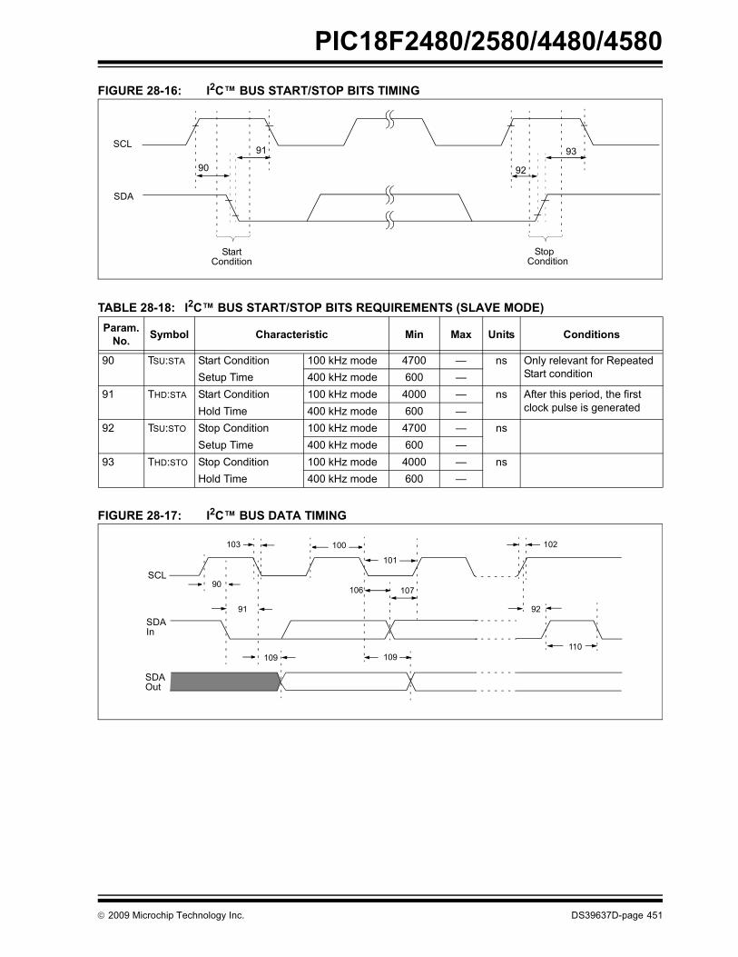
PIC18F2480/2580/4480/4580
FIGURE 28-16: I2C™ BUS START/STOP BITS TIMINGTABLE 28-18: I2C™ BUS START/STOP BITS REQUIREMENTS (SLAVE MODE)
FIGURE 28-17: I2C™ BUS DATA TIMING
Param. No. Symbol Characteristic Min Max Units Conditions
90 TSU:STA Start Condition 100 kHz mode 4700 — ns Only relevant for Repeated Start conditionSetup Time 400 kHz mode 600 —
91 THD:STA Start Condition 100 kHz mode 4000 — ns After this period, the first clock pulse is generatedHold Time 400 kHz mode 600 —
92 TSU:STO Stop Condition 100 kHz mode 4700 — nsSetup Time 400 kHz mode 600 —
93 THD:STO Stop Condition 100 kHz mode 4000 — nsHold Time 400 kHz mode 600 —
91
92
93SCL
SDA
StartCondition
StopCondition
90
90
91 92
100
101
103
106 107
109 109110
102
SCL
SDAIn
SDAOut
© 2009 Microchip Technology Inc. DS39637D-page 451

PIC18F2480/2580/4480/4580
TABLE 28-19: I2C™ BUS DATA REQUIREMENTS (SLAVE MODE)Param. No. Symbol Characteristic Min Max Units Conditions
100 THIGH Clock High Time 100 kHz mode 4.0 — μs PIC18FXXXX must operate at a minimum of 1.5 MHz
400 kHz mode 0.6 — μs PIC18FXXXX must operate at a minimum of 10 MHz
MSSP module 1.5 TCY —101 TLOW Clock Low Time 100 kHz mode 4.7 — μs PIC18FXXXX must operate at
a minimum of 1.5 MHz400 kHz mode 1.3 — μs PIC18FXXXX must operate at
a minimum of 10 MHzMSSP module 1.5 TCY —
102 TR SDA and SCL Rise Time
100 kHz mode — 1000 ns400 kHz mode 20 + 0.1 CB 300 ns CB is specified to be from
10 to 400 pF 103 TF SDA and SCL Fall
Time100 kHz mode — 300 ns400 kHz mode 20 + 0.1 CB 300 ns CB is specified to be from
10 to 400 pF 90 TSU:STA Start Condition Setup
Time100 kHz mode 4.7 — μs Only relevant for Repeated
Start condition400 kHz mode 0.6 — μs91 THD:STA Start Condition Hold
Time 100 kHz mode 4.0 — μs After this period, the first clock
pulse is generated400 kHz mode 0.6 — μs106 THD:DAT Data Input Hold Time 100 kHz mode 0 — ns
400 kHz mode 0 0.9 μs107 TSU:DAT Data Input Setup Time 100 kHz mode 250 — ns (Note 2)
400 kHz mode 100 — ns92 TSU:STO Stop Condition Setup
Time100 kHz mode 4.7 — μs400 kHz mode 0.6 — μs
109 TAA Output Valid from Clock
100 kHz mode — 3500 ns (Note 1)400 kHz mode — — ns
110 TBUF Bus Free Time 100 kHz mode 4.7 — μs Time the bus must be free before a new transmission can start
400 kHz mode 1.3 — μs
D102 CB Bus Capacitive Loading — 400 pF Note 1: As a transmitter, the device must provide this internal minimum delay time to bridge the undefined region (min. 300 ns) of
the falling edge of SCL to avoid unintended generation of Start or Stop conditions.2: A Fast mode I2C™ bus device can be used in a Standard mode I2C bus system, but the requirement TSU:DAT ≥ 250 ns
must then be met. This will automatically be the case if the device does not stretch the LOW period of the SCL signal. If such a device does stretch the LOW period of the SCL signal, it must output the next data bit to the SDA line,TR max. + TSU:DAT = 1000 + 250 = 1250 ns (according to the Standard mode I2C bus specification), before the SCL line is released.
DS39637D-page 452 © 2009 Microchip Technology Inc.

PIC18F2480/2580/4480/4580
FIGURE 28-18: MASTER SSP I2C™ BUS START/STOP BITS TIMING WAVEFORMSTABLE 28-20: MASTER SSP I2C™ BUS START/STOP BITS REQUIREMENTS
FIGURE 28-19: MASTER SSP I2C™ BUS DATA TIMING
Param.No. Symbol Characteristic Min Max Units Conditions
90 TSU:STA Start condition 100 kHz mode 2(TOSC)(BRG + 1) — ns Only relevant for Repeated Start condi-tion
Setup Time 400 kHz mode 2(TOSC)(BRG + 1) —1 MHz mode(1) 2(TOSC)(BRG + 1) —
91 THD:STA Start Condition 100 kHz mode 2(TOSC)(BRG + 1) — ns After this period, the first clock pulse is generatedHold Time 400 kHz mode 2(TOSC)(BRG + 1) —
1 MHz mode(1) 2(TOSC)(BRG + 1) —92 TSU:STO Stop Condition 100 kHz mode 2(TOSC)(BRG + 1) — ns
Setup Time 400 kHz mode 2(TOSC)(BRG + 1) —1 MHz mode(1) 2(TOSC)(BRG + 1) —
93 THD:STO Stop Condition 100 kHz mode 2(TOSC)(BRG + 1) — nsHold Time 400 kHz mode 2(TOSC)(BRG + 1) —
1 MHz mode(1) 2(TOSC)(BRG + 1) —Note 1: Maximum pin capacitance = 10 pF for all I2C pins.
91 93SCL
SDA
StartCondition
StopCondition
90 92
9091 92
100101
103
106107
109 109 110
102
SCL
SDAIn
SDAOut
© 2009 Microchip Technology Inc. DS39637D-page 453

PIC18F2480/2580/4480/4580
TABLE 28-21: MASTER SSP I2C™ BUS DATA REQUIREMENTS Param.No. Symbol Characteristic Min Max Units Conditions
100 THIGH Clock High Time
100 kHz mode 2(TOSC)(BRG + 1) — ms400 kHz mode 2(TOSC)(BRG + 1) — ms1 MHz mode(1) 2(TOSC)(BRG + 1) — ms
101 TLOW Clock Low Time 100 kHz mode 2(TOSC)(BRG + 1) — ms400 kHz mode 2(TOSC)(BRG + 1) — ms1 MHz mode(1) 2(TOSC)(BRG + 1) — ms
102 TR SDA and SCL Rise Time
100 kHz mode — 1000 ns CB is specified to be from 10 to 400 pF 400 kHz mode 20 + 0.1 CB 300 ns
1 MHz mode(1) — 300 ns103 TF SDA and SCL
Fall Time100 kHz mode — 300 ns CB is specified to be from
10 to 400 pF 400 kHz mode 20 + 0.1 CB 300 ns1 MHz mode(1) — 100 ns
90 TSU:STA Start Condition Setup Time
100 kHz mode 2(TOSC)(BRG + 1) — ms Only relevant for Repeated Start condition
400 kHz mode 2(TOSC)(BRG + 1) — ms1 MHz mode(1) 2(TOSC)(BRG + 1) — ms
91 THD:STA Start Condition Hold Time
100 kHz mode 2(TOSC)(BRG + 1) — ms After this period, the first clock pulse is generated400 kHz mode 2(TOSC)(BRG + 1) — ms
1 MHz mode(1) 2(TOSC)(BRG + 1) — ms106 THD:DAT Data Input
Hold Time100 kHz mode 0 — ns400 kHz mode 0 0.9 ms
107 TSU:DAT Data Input Setup Time
100 kHz mode 250 — ns (Note 2)400 kHz mode 100 — ns
92 TSU:STO Stop Condition Setup Time
100 kHz mode 2(TOSC)(BRG + 1) — ms400 kHz mode 2(TOSC)(BRG + 1) — ms1 MHz mode(1) 2(TOSC)(BRG + 1) — ms
109 TAA Output Valid from Clock
100 kHz mode — 3500 ns400 kHz mode — 1000 ns1 MHz mode(1) — — ns
110 TBUF Bus Free Time 100 kHz mode 4.7 — ms Time the bus must be free before a new transmission can start
400 kHz mode 1.3 — ms
D102 CB Bus Capacitive Loading — 400 pF Note 1: Maximum pin capacitance = 10 pF for all I2C™ pins.
2: A Fast mode I2C bus device can be used in a Standard mode I2C bus system, but parameter #107 ≥ 250 ns must then be met. This will automatically be the case if the device does not stretch the LOW period of the SCL signal. If such a device does stretch the LOW period of the SCL signal, it must output the next data bit to the SDA line, parameter #102 + parameter #107 = 1000 + 250 = 1250 ns (for 100 kHz mode), before the SCL line is released.
DS39637D-page 454 © 2009 Microchip Technology Inc.

PIC18F2480/2580/4480/4580
FIGURE 28-20: EUSART SYNCHRONOUS TRANSMISSION (MASTER/SLAVE) TIMINGTABLE 28-22: EUSART SYNCHRONOUS TRANSMISSION REQUIREMENTS
FIGURE 28-21: EUSART SYNCHRONOUS RECEIVE (MASTER/SLAVE) TIMING
TABLE 28-23: EUSART SYNCHRONOUS RECEIVE REQUIREMENTS
Param No. Symbol Characteristic Min Max Units Conditions
120 TCKH2DTV SYNC XMIT (MASTER & SLAVE)Clock High to Data Out Valid PIC18FXXXX — 40 ns
PIC18LFXXXX — 100 ns VDD = 2.0V121 TCKRF Clock Out Rise Time and Fall Time
(Master mode)PIC18FXXXX — 20 nsPIC18LFXXXX — 50 ns VDD = 2.0V
122 TDTRF Data Out Rise Time and Fall Time PIC18FXXXX — 20 nsPIC18LFXXXX — 50 ns VDD = 2.0V
Param. No. Symbol Characteristic Min Max Units Conditions
125 TDTV2CKL SYNC RCV (MASTER & SLAVE)Data Hold before CK ↓ (DT hold time) 10 — ns
126 TCKL2DTL Data Hold after CK ↓ (DT hold time) 15 — ns
121 121
120122
RC6/TX/CK
RC7/RX/DTPin
Pin
125
126
RC6/TX/CK
RC7/RX/DT
Pin
Pin
Note: Refer to Figure 28-4 for load conditions.
© 2009 Microchip Technology Inc. DS39637D-page 455
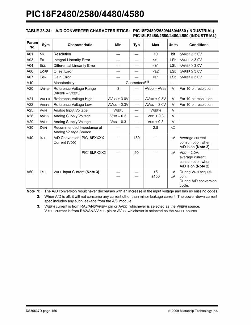
PIC18F2480/2580/4480/4580
TABLE 28-24: A/D CONVERTER CHARACTERISTICS: PIC18F2480/2580/4480/4580 (INDUSTRIAL)PIC18LF2480/2580/4480/4580 (INDUSTRIAL) Param
No. Sym Characteristic Min Typ Max Units Conditions
A01 NR Resolution — — 10 bit ΔVREF ≥ 3.0V A03 EIL Integral Linearity Error — — <±1 LSb ΔVREF ≥ 3.0V A04 EDL Differential Linearity Error — — <±1 LSb ΔVREF ≥ 3.0V A06 EOFF Offset Error — — <±2 LSb ΔVREF ≥ 3.0V A07 EGN Gain Error — — <±1 LSb ΔVREF ≥ 3.0V A10 — Monotonicity Guaranteed(1) —A20 ΔVREF Reference Voltage Range
(VREFH – VREFL)3 — AVDD – AVSS V For 10-bit resolution
A21 VREFH Reference Voltage High AVSS + 3.0V — AVDD + 0.3V V For 10-bit resolutionA22 VREFL Reference Voltage Low AVSS – 0.3V — AVDD – 3.0V V For 10-bit resolutionA25 VAIN Analog Input Voltage VREFL — VREFH VA28 AVDD Analog Supply Voltage VDD – 0.3 — VDD + 0.3 VA29 AVSS Analog Supply Voltage VSS – 0.3 — VSS + 0.3 VA30 ZAIN Recommended Impedance of
Analog Voltage Source— — 2.5 kΩ
A40 IAD A/D ConversionCurrent (VDD)
PIC18FXXXX — 180 — μA Average current consumption when A/D is on (Note 2)
PIC18LFXXXX — 90 — μA VDD = 2.0V;average current consumption when A/D is on (Note 2)
A50 IREF VREF Input Current (Note 3) ——
——
±5±150
μAμA
During VAIN acquisi-tion.During A/D conversion cycle.
Note 1: The A/D conversion result never decreases with an increase in the input voltage and has no missing codes.2: When A/D is off, it will not consume any current other than minor leakage current. The power-down current
spec includes any such leakage from the A/D module.3: VREFH current is from RA3/AN3/VREF+ pin or AVDD, whichever is selected as the VREFH source.
VREFL current is from RA2/AN2/VREF- pin or AVSS, whichever is selected as the VREFL source.
DS39637D-page 456 © 2009 Microchip Technology Inc.

PIC18F2480/2580/4480/4580
FIGURE 28-22: A/D CONVERSION TIMINGTABLE 28-25: A/D CONVERSION REQUIREMENTS Param
No. Symbol Characteristic Min Max Units Conditions
130 TAD A/D Clock Period PIC18FXXXX 0.7 25.0(1) μs TOSC based, VREF ≥ 3.0VPIC18LFXXXX 1.4 25.0(1) μs VDD = 2.0V;
TOSC based, VREF full rangePIC18FXXXX — 1 μs A/D RC modePIC18LFXXXX — 3 μs VDD = 2.0V;
A/D RC mode131 TCNV Conversion Time
(not including acquisition time) (Note 2)11 12 TAD
132 TACQ Acquisition Time (Note 3) 1.4 — μs -40°C to +85°C135 TSWC Switching Time from Convert → Sample — (Note 4) —136 TAMP Amplifier Settling Time (Note 5) 1 — μs This may be used if the “new” input
voltage has not changed by more than 1 LSb (i.e., 5 mV @ 5.12V) from the last sampled voltage (as stated on CHOLD).
Note 1: The time of the A/D clock period is dependent on the device frequency and the TAD clock divider. 2: ADRES register may be read on the following TCY cycle.3: The time for the holding capacitor to acquire the “New” input voltage when the voltage changes full scale
after the conversion (AVDD to AVSS or AVSS to AVDD). The source impedance (RS) on the input channels is 50Ω.
4: On the following cycle of the device clock. 5: See Section 20.0 “10-Bit Analog-to-Digital Converter (A/D) Module” for minimum conditions when input
voltage has changed more than 1 LSb.
131
130
132
BSF ADCON0, GO
Q4
A/D CLK
A/D DATA
ADRES
ADIF
GO
SAMPLE
OLD_DATA
SAMPLING STOPPED
DONE
NEW_DATA
(Note 2)
9 8 7 2 1 0
Note 1: If the A/D clock source is selected as RC, a time of TCY is added before the A/D clock starts. This allows the SLEEP instructionto be executed.
2: This is a minimal RC delay (typically 100 ns), which also disconnects the holding capacitor from the analog input.
. . . . . .
TCY
© 2009 Microchip Technology Inc. DS39637D-page 457

PIC18F2480/2580/4480/4580
NOTES:DS39637D-page 458 © 2009 Microchip Technology Inc.

PIC18F2480/2580/4480/4580
29.0 PACKAGING INFORMATION
29.1 Package Marking Information
28-Lead SPDIP
XXXXXXXXXXXXXXXXXXXXXXXXXXXXXXXXXX
YYWWNNN
Example
PIC18F2580-I/SP0910017
28-Lead SOIC
XXXXXXXXXXXXXXXXXXXXXXXXXXXXXXXXXXXXXXXXXXXXXXXXXXXXXXXXXXXX
YYWWNNN
Example
PIC18F2580-E/SO0910017
28-Lead QFN
XXXXXXXXXXXXXXXXYYWWNNN
Example
18F2580-I/ML0910017
3e
3e
3e
Legend: XX...X Customer-specific informationY Year code (last digit of calendar year)YY Year code (last 2 digits of calendar year)WW Week code (week of January 1 is week ‘01’)NNN Alphanumeric traceability code Pb-free JEDEC designator for Matte Tin (Sn)* This package is Pb-free. The Pb-free JEDEC designator ( )
can be found on the outer packaging for this package.
Note: In the event the full Microchip part number cannot be marked on one line, it willbe carried over to the next line, thus limiting the number of availablecharacters for customer-specific information.
3e
3e
© 2009 Microchip Technology Inc. DS39637D-page 459

PIC18F2480/2580/4480/4580
29.1 Package Marking Information (Continued)44-Lead TQFP
XXXXXXXXXXXXXXXXXXXXXXXXXXXXXX
YYWWNNN
Example
PIC18F4580-I/PT
0910017
XXXXXXXXXX
44-Lead QFN
XXXXXXXXXXXXXXXXXXXX
YYWWNNN
PIC18F4580
Example
-I/ML0910017
40-Lead PDIP
XXXXXXXXXXXXXXXXXXXXXXXXXXXXXXXXXXXX
XXXXXXXXXXXXXXXXXXYYWWNNN
Example
PIC18F4580-I/P0910017
3e
3e
3e
DS39637D-page 460 © 2009 Microchip Technology Inc.

PIC18F2480/2580/4480/4580
29.2 Package DetailsThe following sections give the technical details of the packages.!" !"#$%&"' ()"&'"!&)&#*&&&# +%&,&!&- '!!#.#&"#'#%!&"!!#%!&"!!!&$#/!# '!#&.0
1,2 1!'! &$& "!**&"&&!
!" 3&'!&"&4#*!(!!&4%&&#&&&255***''54
6&! 7,8.'!9'&! 7 7: ;
7"')%! 7 <& 1, && = = ##4 4!! - 1!&& = ="#&"#>#& . - --##4>#& . < : 9& - -? && 9 - 9# 4!! < 69#>#& ) 9*9#>#& ) < : *+ 1 = = -
NOTE 1
N
1 2
D
E1
eB
c
E
L
A2
eb
b1A1
A
3
* ,1
© 2009 Microchip Technology Inc. DS39637D-page 461

PIC18F2480/2580/4480/4580
# #$%&'(#)
!" !"#$%&"' ()"&'"!&)&#*&&&# +%&,&!&- '!!#.#&"#'#%!&"!!#%!&"!!!&$#''!# '!#&.0
1,2 1!'! &$& "!**&"&&!.32 %'!("!"*&"&&(%%'&"!!
!" 3&'!&"&4#*!(!!&4%&&#&&&255***''54
6&! 99. .'!9'&! 7 7: ;
7"')%! 7 <& 1,: 8& = = ?##4 4!! = =&#%%+ = -: >#& . -1,##4>#& . 1,: 9& 1,,'%@&A = 3&9& 9 = 3&& 9 .33& B = <B9# 4!! < = --9#>#& ) - = #%& B = B#%&1&&' B = B
c
hh
LL1
A2
A1
A
NOTE 1
1 2 3
be
EE1
D
φ
β
α
N
* ,1
DS39637D-page 462 © 2009 Microchip Technology Inc.

PIC18F2480/2580/4480/4580
*+%!,-./.*+! 01'(() ,1
!" !"#$%&"' ()"&'"!&)&#*&&&# 4!!*!"&#- '!#&.0
1,2 1!'! &$& "!**&"&&!.32 %'!("!"*&"&&(%%'&"!!
!" 3&'!&"&4#*!(!!&4%&&#&&&255***''54
6&! 99. .'!9'&! 7 7: ;
7"')%! 7 <& ?1,: 8& < &#%% ,&& 4!! - .3: >#& . ?1,.$!##>#& . -? - : 9& ?1,.$!##9& -? - ,&&>#& ) - - -,&&9& 9 ,&&&.$!## C = =
D EXPOSED D2
e
b
K
E2
E
L
N
NOTE 1
1
22
1
N
A
A1A3
TOP VIEW BOTTOM VIEW
PAD
* ,1
© 2009 Microchip Technology Inc. DS39637D-page 463

PIC18F2480/2580/4480/4580
*+%!,-./.*+! 01'(() ,1
!" 3&'!&"&4#*!(!!&4%&&#&&&255***''54
DS39637D-page 464 © 2009 Microchip Technology Inc.

PIC18F2480/2580/4480/4580
2 .
!" !"#$%&"' ()"&'"!&)&#*&&&# +%&,&!&- '!!#.#&"#'#%!&"!!#%!&"!!!&$#/!# '!#&.0
1,2 1!'! &$& "!**&"&&!
!" 3&'!&"&4#*!(!!&4%&&#&&&255***''54
6&! 7,8.'!9'&! 7 7: ;
7"')%! 7 & 1, && = = ##4 4!! = 1!&& = ="#&"#>#& . = ?##4>#& . < = <: 9& < = && 9 = 9# 4!! < = 69#>#& ) - = 9*9#>#& ) = -: *+ 1 = =
N
NOTE 1
E1
D
1 2 3
A
A1b1
b e
c
eB
E
L
A2
* ,?1
© 2009 Microchip Technology Inc. DS39637D-page 465

PIC18F2480/2580/4480/4580
2231 *+435/5/5%'3*+
!" !"#$%&"' ()"&'"!&)&#*&&&# ,'%!&!&D!E' - '!!#.#&"#'#%!&"!!#%!&"!!!&$#''!# '!#&.0
1,2 1!'! &$& "!**&"&&!.32 %'!("!"*&"&&(%%'&"!!
!" 3&'!&"&4#*!(!!&4%&&#&&&255***''54
6&! 99. .'!9'&! 7 7: ;
7"')%9#! 7 9#& <1,: 8& = = ##4 4!! &#%% = 3&9& 9 ? 3&& 9 .33& B -B B: >#& . 1,: 9& 1,##4>#& . 1,##49& 1,9# 4!! = 9#>#& ) - - #%& B B -B#%&1&&' B B -B
A
E
E1
DD1
e
b
NOTE 1NOTE 2
N
1 2 3
c
A1L
A2L1
α
φ
β
* ,?1
DS39637D-page 466 © 2009 Microchip Technology Inc.

PIC18F2480/2580/4480/4580
2231 *+435/5/5%'3*+
!" 3&'!&"&4#*!(!!&4%&&#&&&255***''54
© 2009 Microchip Technology Inc. DS39637D-page 467

PIC18F2480/2580/4480/4580
22*+%!,-/*+!
!" !"#$%&"' ()"&'"!&)&#*&&&# 4!!*!"&#- '!#&.0
1,2 1!'! &$& "!**&"&&!.32 %'!("!"*&"&&(%%'&"!!
!" 3&'!&"&4#*!(!!&4%&&#&&&255***''54
6&! 99. .'!9'&! 7 7: ;
7"')%! 7 & ?1,: 8& < &#%% ,&& 4!! - .3: >#& . <1,.$!##>#& . ?- ? ?<: 9& <1,.$!##9& ?- ? ?<,&&>#& ) - -<,&&9& 9 - ,&&&.$!## C = =
D EXPOSEDPAD
D2
e
b
KL
E2
21
NNOTE 1
21
E
N
BOTTOM VIEWTOP VIEW
A3 A1
A
* ,-1
DS39637D-page 468 © 2009 Microchip Technology Inc.

PIC18F2480/2580/4480/4580
22*+%!,-/*+!
!" 3&'!&"&4#*!(!!&4%&&#&&&255***''54
© 2009 Microchip Technology Inc. DS39637D-page 469

PIC18F2480/2580/4480/4580
NOTES:DS39637D-page 470 © 2009 Microchip Technology Inc.

PIC18F2480/2580/4480/4580
APPENDIX A: REVISION HISTORY
Revision A (July 2004)Original data sheet for PIC18F2480/2580/4480/4580devices.
Revision B (August 2006)Edits to Table 6-1 in Section 6.0 “Memory Organization”and trademarking updated.
Revision C (March 2007)Edits to Table 6-1 in Section 6.0 “Memory Organiza-tion”, pin name change in Section 22.5 “ConnectionConsiderations”, updates to Section 27.3 “DC Charac-teristics”, changes to SPI Mode Requirements inFigure 28-12 and Figure 28-13, and Table 28-14 throughTable 28-17, and there have been minor updates to thedata sheet text, including trademarking updates.
Revision D (November 2009)Removed Preliminary from the Condition tags. Variousedits throughout the data sheet text.
APPENDIX B: DEVICE DIFFERENCES
The differences between the devices listed in this datasheet are shown in Table B-1.
TABLE B-1: DEVICE DIFFERENCES Features PIC18F2480 PIC18F2580 PIC18F4480 PIC18F4580
Program Memory (Bytes) 16384 32768 16384 32768Program Memory (Instructions) 8192 16384 8291 16384Interrupt Sources 19 19 20 20I/O Ports Ports A, B, C, (E) Ports A, B, C, (E) Ports A, B, C, D, E Ports A, B, C, D, ECapture/Compare/PWM Modules 1 1 1 1Enhanced Capture/Compare/PWM Modules
0 0 1 1
Parallel Communications (PSP) No No Yes Yes10-bit Analog-to-Digital Module 8 input channels 8 input channels 11 input channels 11 input channelsPackages 28-pin SPDIP
28-pin SOIC28-pin QFN
28-pin SPDIP28-pin SOIC28-pin QFN
40-pin PDIP44-pin TQFP44-pin QFN
40-pin PDIP44-pin TQFP44-pin QFN
© 2009 Microchip Technology Inc. DS39637D-page 471

PIC18F2480/2580/4480/4580
APPENDIX C: CONVERSION CONSIDERATIONS
This appendix discusses the considerations forconverting from previous versions of a device to theones listed in this data sheet. Typically, these changesare due to the differences in the process technologyused. An example of this type of conversion is from aPIC16C74A to a PIC16C74B.
Not Applicable
APPENDIX D: MIGRATION FROM BASELINE TO ENHANCED DEVICES
This section discusses how to migrate from a Baselinedevice (i.e., PIC16C5X) to an Enhanced MCU device(i.e., PIC18FXXX).
The following are the list of modifications over thePIC16C5X microcontroller family:
Not Currently Available
DS39637D-page 472 © 2009 Microchip Technology Inc.

PIC18F2480/2580/4480/4580
APPENDIX E: MIGRATION FROM MID-RANGE TO ENHANCED DEVICES
A detailed discussion of the differences between themid-range MCU devices (i.e., PIC16CXXX) and theenhanced devices (i.e., PIC18FXXX) is provided inAN716, “Migrating Designs from PIC16C74A/74B toPIC18C442.” The changes discussed, while devicespecific, are generally applicable to all mid-range toenhanced device migrations.
This Application Note is available as Literature NumberDS00716.
APPENDIX F: MIGRATION FROM HIGH-END TO ENHANCED DEVICES
A detailed discussion of the migration pathway anddifferences between the high-end MCU devices (i.e., PIC17CXXX) and the enhanced devices (i.e., PIC18FXXX) is provided in AN726, “PIC17CXXXto PIC18CXXX Migration.” This Application Note isavailable as Literature Number DS00726.
© 2009 Microchip Technology Inc. DS39637D-page 473

PIC18F2480/2580/4480/4580
NOTES:DS39637D-page 474 © 2009 Microchip Technology Inc.

PIC18F2480/2580/4480/4580
INDEXAA/D ................................................................................... 253
A/D Converter Interrupt, Configuring ....................... 257Acquisition Requirements ........................................ 258ADCON0 Register .................................................... 253ADCON1 Register .................................................... 253ADCON2 Register .................................................... 253ADRESH Register ............................................ 253, 256ADRESL Register .................................................... 253Analog Port Pins, Configuring .................................. 260Associated Registers ............................................... 262Automatic Acquisition Time ...................................... 259Calculating the Minimum Required
Acquisition Time .............................................. 258Configuring the Module ............................................ 257Conversion Clock (TAD) Selection ........................... 259Conversion Status (GO/DONE Bit) .......................... 256Conversions ............................................................. 261Converter Characteristics ........................................ 456Operation in Power-Managed Modes ...................... 260Special Event Trigger (CCP) .................................... 262Special Event Trigger (ECCP) ................................. 178Use of the CCP1 Trigger .......................................... 262
Absolute Maximum Ratings ............................................. 421AC (Timing) Characteristics ............................................. 438
Load Conditions for Device Timing Specifications ................................................... 439
Parameter Symbology ............................................. 438Temperature and Voltage Specifications ................. 439Timing Conditions .................................................... 439
Access Bank ...................................................................... 76Mapping with Indexed Literal Offset Mode ............... 100
ACKSTAT ........................................................................ 221ACKSTAT Status Flag ..................................................... 221ADCON0 Register ............................................................ 253
GO/DONE Bit ........................................................... 256ADCON1 Register ............................................................ 253ADCON2 Register ............................................................ 253ADDFSR .......................................................................... 410ADDLW ............................................................................ 373ADDULNK ........................................................................ 410ADDWF ............................................................................ 373ADDWFC ......................................................................... 374ADRESH Register ............................................................ 253ADRESL Register .................................................... 253, 256Analog-to-Digital Converter. See A/D.and BSR ........................................................................... 100ANDLW ............................................................................ 374ANDWF ............................................................................ 375Assembler
MPASM Assembler .................................................. 418Auto-Wake-up on Sync Break Character ......................... 246
BBank Select Register (BSR) ............................................... 73Baud Rate Generator ....................................................... 217Baud Rate Generator (BRG) ............................................ 235BC .................................................................................... 375BCF .................................................................................. 376BF .................................................................................... 221BF Status Flag ................................................................. 221
Bit Timing Configuration RegistersBRGCON1 ............................................................... 344BRGCON2 ............................................................... 344BRGCON3 ............................................................... 344
Block DiagramsA/D ........................................................................... 256Analog Input Model .................................................. 257Baud Rate Generator .............................................. 217CAN Buffers and Protocol Engine ........................... 280Capture Mode Operation ......................................... 170Comparator I/O Operating Modes ........................... 264Comparator Output .................................................. 266Comparator Voltage Reference ............................... 270Comparator Voltage Reference
Output Buffer Example .................................... 271Compare Mode Operation ....................................... 171Device Clock .............................................................. 34Enhanced PWM ....................................................... 179EUSART Receive .................................................... 244EUSART Transmit ................................................... 242External Power-on Reset Circuit
(Slow VDD Power-up) ........................................ 49Fail-Safe Clock Monitor ........................................... 361Generic I/O Port ....................................................... 135High/Low-Voltage Detect with External Input .......... 274MSSP (I2C Master Mode) ........................................ 215MSSP (I2C Mode) .................................................... 200MSSP (SPI Mode) ................................................... 191On-Chip Reset Circuit ................................................ 47PIC18F2480/2580 ..................................................... 12PIC18F4480/4580 ..................................................... 13PLL (HS Mode) .......................................................... 31PORTD and PORTE (Parallel Slave Port) ............... 149PWM Operation (Simplified) .................................... 173Reads From Flash Program Memory ...................... 105Single Comparator ................................................... 265Table Read Operation ............................................. 101Table Write Operation ............................................. 102Table Writes to Flash Program Memory .................. 107Timer0 in 16-Bit Mode ............................................. 152Timer0 in 8-Bit Mode ............................................... 152Timer1 ..................................................................... 156Timer1 (16-Bit Read/Write Mode) ............................ 156Timer2 ..................................................................... 162Timer3 ..................................................................... 164Timer3 (16-Bit Read/Write Mode) ............................ 164Transmit Buffers ...................................................... 334Watchdog Timer ...................................................... 358
Block Diagrams Comparator Analog Input Model ............ 267BN .................................................................................... 376BNC ................................................................................. 377BNN ................................................................................. 377BNOV .............................................................................. 378BNZ ................................................................................. 378BOR. See Brown-out Reset.BOV ................................................................................. 381BRA ................................................................................. 379BRG. See Baud Rate Generator.Brown-out Reset (BOR) ..................................................... 50
Detecting ................................................................... 50Disabling in Sleep Mode ............................................ 50Software Enabled ...................................................... 50
© 2009 Microchip Technology Inc. DS39637D-page 475

PIC18F2480/2580/4480/4580
BSF .................................................................................. 379BTFSC ............................................................................. 380BTFSS .............................................................................. 380BTG .................................................................................. 381BZ ..................................................................................... 382CC Compilers
MPLAB C18 ............................................................. 418CALL ................................................................................ 382CALLW ............................................................................. 411CAN Module
External-Internal Clock in HS-PLL Based Oscillators ............................................. 339
Capture (CCP Module) ..................................................... 169Associated Registers ............................................... 172CCP1/ECCP1 Pin Configuration .............................. 169CCPR1H:CCPR1L Registers ................................... 169Software Interrupt .................................................... 169Timer1/Timer3 Mode Selection ................................ 169
Capture (ECCP Module) .................................................. 178Capture/Compare/PWM (CCP) ........................................ 167
Capture Mode. See Capture.CCP Mode and Timer Resources ............................ 168CCPRxH Register .................................................... 168CCPRxL Register ..................................................... 168Compare Mode. See Compare.Interaction Between CCP1 and ECCP1
for Timer Resources ........................................ 168Module Configuration ............................................... 168PWM Mode. See PWM.
Clock Sources .................................................................... 34Selecting the 31 kHz Source ...................................... 35Selection Using OSCCON Register ........................... 35
Clocking Scheme/Instruction Cycle .................................... 71CLRF ................................................................................ 383CLRWDT .......................................................................... 383Code Examples
16 x 16 Signed Multiply Routine .............................. 11816 x 16 Unsigned Multiply Routine .......................... 1188 x 8 Signed Multiply Routine .................................. 1178 x 8 Unsigned Multiply Routine .............................. 117Changing Between Capture Prescalers ................... 169Changing to Configuration Mode ............................. 284Computed GOTO Using an Offset Value ................... 70Data EEPROM Read ............................................... 113Data EEPROM Refresh Routine .............................. 114Data EEPROM Write ............................................... 113Erasing a Flash Program Memory Row ................... 106Fast Register Stack .................................................... 70How to Clear RAM (Bank 1) Using
Indirect Addressing ............................................ 95Implementing a Real-Time Clock Using
a Timer1 Interrupt Service ............................... 159Initializing PORTA .................................................... 135Initializing PORTB .................................................... 138Initializing PORTC .................................................... 141Initializing PORTD .................................................... 143Initializing PORTE .................................................... 146Loading the SSPBUF (SSPSR) Register ................. 194Reading a CAN Message ........................................ 299Reading a Flash Program Memory Word ................ 105Saving STATUS, WREG and BSR
Registers in RAM ............................................. 134Transmitting a CAN Message Using
Banked Method ................................................ 292
Transmitting a CAN Message Using WIN Bits ......... 292WIN and ICODE Bits Usage in Interrupt Service
Routine to Access TX/RX Buffers .................... 284Writing to Flash Program Memory ................... 108–109
Code Protection ............................................................... 349COMF .............................................................................. 384Comparator ...................................................................... 263
Analog Input Connection Considerations ................ 267Associated Registers ............................................... 267Configuration ........................................................... 264Effects of a Reset .................................................... 266Interrupts ................................................................. 266Operation ................................................................. 265Operation During Sleep ........................................... 266Outputs .................................................................... 265Reference ................................................................ 265
External Signal ................................................ 265Internal Signal .................................................. 265
Response Time ........................................................ 265Comparator Specifications ............................................... 436Comparator Voltage Reference ....................................... 269
Accuracy and Error .................................................. 270Associated Registers ............................................... 271Configuring .............................................................. 269Connection Considerations ...................................... 270Effects of a Reset .................................................... 270Operation During Sleep ........................................... 270
Compare (CCP Module) .................................................. 171Associated Registers ............................................... 172CCP Pin Configuration ............................................. 171CCPR1 Register ...................................................... 171Software Interrupt .................................................... 171Special Event Trigger .............................. 165, 171, 262Timer1/Timer3 Mode Selection ................................ 171
Compare (ECCP Module) ................................................ 178Special Event Trigger .............................................. 178
Configuration Bits ............................................................ 349Configuration Mode ......................................................... 330Configuration Register Protection .................................... 366Context Saving During Interrupts ..................................... 134Conversion Considerations .............................................. 472CPFSEQ .......................................................................... 384CPFSGT .......................................................................... 385CPFSLT ........................................................................... 385Crystal Oscillator/Ceramic Resonator ................................ 29Customer Change Notification Service ............................ 486Customer Notification Service ......................................... 486Customer Support ............................................................ 486
DData Addressing Modes .................................................... 95
Comparing Addressing Modes with the Extended Instruction Set Enabled ..................... 99
Direct ......................................................................... 95Indexed Literal Offset ................................................ 98Indirect ....................................................................... 95Inherent and Literal .................................................... 95
Data EEPROM Code Protection ...................................... 366Data EEPROM Memory ................................................... 111
Associated Registers ............................................... 115EEADR Register ...................................................... 111EECON1 and EECON2 Registers ........................... 111Operation During Code-Protect ............................... 114Protection Against Spurious Write ........................... 114Reading ................................................................... 113Using ....................................................................... 114
DS39637D-page 476 © 2009 Microchip Technology Inc.

PIC18F2480/2580/4480/4580
Write Verify .............................................................. 113Writing ...................................................................... 113Data Memory ..................................................................... 73Access Bank .............................................................. 76and the Extended Instruction Set ............................... 98Bank Select Register (BSR) ....................................... 73General Purpose Registers ........................................ 76Map for PIC18F2480/4480 ......................................... 74Map for PIC18F2580/4580 ......................................... 75Special Function Registers ........................................ 77
DAW ................................................................................. 386DC Characteristics ........................................................... 433
Power-Down and Supply Current ............................ 424Supply Voltage ......................................................... 423
DCFSNZ .......................................................................... 387DECF ............................................................................... 386DECFSZ ........................................................................... 387Development Support ...................................................... 417Device Differences ........................................................... 471Device Overview .................................................................. 9
Features (table) .......................................................... 11Device Reset Timers .......................................................... 51
Oscillator Start-up Timer (OST) ................................. 51PLL Lock Time-out ..................................................... 51Power-up Timer (PWRT) ........................................... 51
Direct Addressing ............................................................... 96
EECAN Module .................................................................. 279
Baud Rate Setting .................................................... 338Bit Time Partitioning ................................................. 338Bit Timing Configuration Registers .......................... 344Calculating TQ, Nominal Bit Rate and
Nominal Bit Time ............................................. 341CAN Baud Rate Registers ....................................... 317CAN Control and Status Registers .......................... 281CAN Controller Register Map .................................. 325CAN I/O Control Register ......................................... 320CAN Interrupt Registers ........................................... 321CAN Interrupts ......................................................... 345
Acknowledge ................................................... 347Bus Activity Wake-up ....................................... 346Bus-Off ............................................................. 347Code Bits ......................................................... 346Error ................................................................. 346Message Error ................................................. 346Receive ............................................................ 346Receiver Bus Passive ...................................... 347Receiver Overflow ........................................... 347Receiver Warning ............................................ 347Transmit ........................................................... 346Transmitter Bus Passive .................................. 347Transmitter Warning ........................................ 347
CAN Message Buffers ............................................. 332Dedicated Receive ........................................... 332Dedicated Transmit .......................................... 332Programmable Auto-RTR ................................ 333Programmable Transmit/Receive .................... 332
CAN Message Transmission ................................... 333Aborting ........................................................... 333Initiating ........................................................... 333Priority .............................................................. 334
CAN Modes of Operation ......................................... 330CAN Registers ......................................................... 281Configuration Mode .................................................. 330Dedicated CAN Receive Buffer Registers ............... 293
Dedicated CAN Transmit Buffer Registers .............. 288Disable Mode ........................................................... 330Error Detection ........................................................ 344
Acknowledge ................................................... 344Bit .................................................................... 344CRC ................................................................. 344Error Modes and Counters .............................. 344Error States ..................................................... 344Form ................................................................ 344Stuff Bit ............................................................ 344
Error Modes State (diagram) ................................... 345Error Recognition Mode ........................................... 331Filter-Mask Truth (table) .......................................... 336Functional Modes .................................................... 331
Mode 0 (Legacy Mode) .................................... 331Mode 1 (Enhanced Legacy Mode) .................. 331Mode 2 (Enhanced FIFO Mode) ...................... 332
Information Processing Time (IPT) .......................... 341Lengthening a Bit Period ......................................... 343Listen Only Mode ..................................................... 331Loopback Mode ....................................................... 331Message Acceptance Filters and Masks ......... 308, 336Message Acceptance Mask and
Filter Operation ................................................ 337Message Reception ................................................. 335
Enhanced FIFO Mode ..................................... 336Priority ............................................................. 335Time-Stamping ................................................ 336
Normal Mode ........................................................... 330Oscillator Tolerance ................................................. 343Overview .................................................................. 279Phase Buffer Segments ........................................... 341Programmable TX/RX and Auto-RTR Buffers ......... 300Programming Time Segments ................................. 343Propagation Segment .............................................. 341Sample Point ........................................................... 341Shortening a Bit Period ............................................ 343Synchronization ....................................................... 342
Hard ................................................................. 342Resynchronization ........................................... 342Rules ............................................................... 342
Synchronization Segment ........................................ 341Time Quanta ............................................................ 341Values for ICODE (table) ......................................... 346
ECCPCapture and Compare Modes ................................. 178Standard PWM Mode .............................................. 178
Effect on Standard Instructions .......................................... 98Effect on Standard PIC Instructions ................................. 414Effects of Power-Managed Modes on
Various Clock Sources .............................................. 37Electrical Characteristics ................................................. 421Enhanced Capture/Compare/PWM (ECCP) .................... 177
Capture Mode. See Capture (ECCP Module).Outputs and Configuration ....................................... 178Pin Configurations for ECCP Modes ....................... 178PWM Mode. See PWM (ECCP Module).Timer Resources ..................................................... 178
Enhanced PWM Mode. See PWM (ECCP Module). ....... 179Enhanced Universal Synchronous Receiver
Transmitter (EUSART). See EUSART.Equations
A/D Acquisition Time ............................................... 258A/D Minimum Charging Time .................................. 258
Errata ................................................................................... 7
© 2009 Microchip Technology Inc. DS39637D-page 477

PIC18F2480/2580/4480/4580
Error Recognition Mode ................................................... 330EUSARTAsynchronous Mode ................................................ 241Associated Registers, Receive ........................ 245Associated Registers, Transmit ....................... 243Auto-Wake-up on Sync Break .......................... 246Break Character Sequence .............................. 247Receiver ........................................................... 244Setting up 9-Bit Mode with Address Detect ..... 244Transmitter ....................................................... 241
Baud Rate Generator (BRG)Associated Registers ....................................... 236Auto-Baud Rate Detect .................................... 239Baud Rate Error, Calculating ........................... 236Baud Rates, Asynchronous Modes .................. 237High Baud Rate Select (BRGH Bit) .................. 235Operation in Power-Managed Mode ................ 235Sampling .......................................................... 235
Synchronous Master Mode ...................................... 248Associated Registers, Receive ........................ 250Associated Registers, Transmit ....................... 249Reception ......................................................... 250Transmission .................................................... 248
Synchronous Slave Mode ........................................ 251Associated Registers, Receive ........................ 252Associated Registers, Transmit ....................... 251Reception ......................................................... 252Transmission .................................................... 251
Extended Instruction SetADDFSR .................................................................. 410ADDULNK ................................................................ 410CALLW ..................................................................... 411MOVSF .................................................................... 411MOVSS .................................................................... 412PUSHL ..................................................................... 412SUBFSR .................................................................. 413SUBULNK ................................................................ 413
External Clock Input ........................................................... 30
FFail-Safe Clock Monitor ............................................ 349, 361
Interrupts in Power-Managed Modes ....................... 362POR or Wake-up from Sleep ................................... 362WDT During Oscillator Failure ................................. 361
Fast Register Stack ............................................................ 70Firmware Instructions ....................................................... 367Flash Program Memory .................................................... 101
Associated Registers ............................................... 109Control Registers ..................................................... 102
EECON1 and EECON2 ................................... 102TABLAT (Table Latch) Register ....................... 104TBLPTR (Table Pointer) Register .................... 104
Erase Sequence ...................................................... 106Erasing ..................................................................... 106Operation During Code-Protect ............................... 109Reading .................................................................... 105Table Pointer
Boundaries Based on Operation ...................... 104Table Pointer Boundaries ........................................ 104Table Reads and Table Writes ................................ 101Write Sequence ....................................................... 107Writing To ................................................................. 107
Protection Against Spurious Writes ................. 109Unexpected Termination .................................. 109Write Verify ...................................................... 109
FSCM. See Fail-Safe Clock Monitor.
GGOTO .............................................................................. 388
HHardware Multiplier
Introduction .............................................................. 117Operation ................................................................. 117Performance Comparison ........................................ 117
High/Low-Voltage Detect ................................................. 273Applications ............................................................. 276Associated Registers ............................................... 277Characteristics ......................................................... 437Current Consumption ............................................... 275Effects of a Reset .................................................... 277Operation ................................................................. 274
During Sleep .................................................... 277Setup ....................................................................... 275Start-up Time ........................................................... 275Typical Application ................................................... 276
HLVD. See High/Low-Voltage Detect. ............................. 273
II/O Ports ........................................................................... 135I2C Mode (MSSP)
Acknowledge Sequence Timing .............................. 224Baud Rate Generator .............................................. 217Bus Collision
During a Repeated Start Condition .................. 228During a Stop Condition .................................. 229
Clock Arbitration ...................................................... 218Clock Stretching ....................................................... 210
10-Bit Slave Receive Mode (SEN = 1) ............ 21010-Bit Slave Transmit Mode ............................ 2107-Bit Slave Receive Mode (SEN = 1) .............. 2107-Bit Slave Transmit Mode .............................. 210
Clock Synchronization and the CKP Bit (SEN = 1) ......................................................... 211
Effect of a Reset ...................................................... 225General Call Address Support ................................. 214I2C Clock Rate w/BRG ............................................. 217Master Mode ............................................................ 215
Operation ......................................................... 216Reception ........................................................ 221Repeated Start Condition Timing .................... 220Start Condition ................................................. 219Transmission ................................................... 221Transmit Sequence ......................................... 216
Multi-Master Communication, Bus Collision and Arbitration ................................................. 225
Multi-Master Mode ................................................... 225Operation ................................................................. 204Read/Write Bit Information (R/W Bit) ............... 204, 205Registers ................................................................. 200Serial Clock (RC3/SCK/SCL) ................................... 205Slave Mode .............................................................. 204
Addressing ....................................................... 204Reception ........................................................ 205Transmission ................................................... 205
Sleep Operation ....................................................... 225Stop Condition Timing ............................................. 224
ID Locations ............................................................. 349, 366INCF ................................................................................ 388INCFSZ ............................................................................ 389In-Circuit Debugger .......................................................... 366In-Circuit Serial Programming (ICSP) ...................... 349, 366
DS39637D-page 478 © 2009 Microchip Technology Inc.
PIC18F2480/2580/4480/4580
Indexed Literal Offset Addressing Mode .......................... 414and Standard PIC18 Instructions ............................. 414Indexed Literal Offset Mode ....................................... 98, 100Indirect Addressing ............................................................ 96INFSNZ ............................................................................ 389Initialization Conditions for all Registers ...................... 55–66Instruction Cycle ................................................................ 71Instruction Flow/Pipelining ................................................. 71Instruction Set .................................................................. 367
ADDLW .................................................................... 373ADDWF .................................................................... 373ADDWF (Indexed Literal Offset mode) .................... 415ADDWFC ................................................................. 374ANDLW .................................................................... 374ANDWF .................................................................... 375BC ............................................................................ 375BCF .......................................................................... 376BN ............................................................................ 376BNC ......................................................................... 377BNN ......................................................................... 377BNOV ....................................................................... 378BNZ .......................................................................... 378BOV ......................................................................... 381BRA .......................................................................... 379BSF .......................................................................... 379BSF (Indexed Literal Offset mode) .......................... 415BTFSC ..................................................................... 380BTFSS ..................................................................... 380BTG .......................................................................... 381BZ ............................................................................ 382CALL ........................................................................ 382CLRF ........................................................................ 383CLRWDT .................................................................. 383COMF ...................................................................... 384CPFSEQ .................................................................. 384CPFSGT .................................................................. 385CPFSLT ................................................................... 385DAW ......................................................................... 386DCFSNZ .................................................................. 387DECF ....................................................................... 386DECFSZ ................................................................... 387Extended Instructions .............................................. 409
and Using MPLAB Tools .................................. 416Considerations when Enabling ........................ 414Syntax .............................................................. 409
General Format ........................................................ 369GOTO ...................................................................... 388INCF ......................................................................... 388INCFSZ .................................................................... 389INFSNZ .................................................................... 389IORLW ..................................................................... 390IORWF ..................................................................... 390LFSR ........................................................................ 391MOVF ....................................................................... 391MOVFF .................................................................... 392MOVLB .................................................................... 392MOVLW ................................................................... 393MOVWF ................................................................... 393MULLW .................................................................... 394MULWF .................................................................... 394NEGF ....................................................................... 395NOP ......................................................................... 395POP ......................................................................... 396PUSH ....................................................................... 396RCALL ..................................................................... 397
RESET ..................................................................... 397RETFIE .................................................................... 398RETLW .................................................................... 398RETURN .................................................................. 399RLCF ....................................................................... 399RLNCF ..................................................................... 400RRCF ....................................................................... 400RRNCF .................................................................... 401SETF ....................................................................... 401SETF (Indexed Literal Offset mode) ........................ 415SLEEP ..................................................................... 402Standard Instructions ............................................... 367SUBFWB ................................................................. 402SUBLW .................................................................... 403SUBWF .................................................................... 403SUBWFB ................................................................. 404Summary Table ....................................................... 370SWAPF .................................................................... 404TBLRD ..................................................................... 405TBLWT .................................................................... 406TSTFSZ ................................................................... 407XORLW ................................................................... 407XORWF ................................................................... 408
INTCON Registers ........................................................... 121Inter-Integrated Circuit. See I2C.Internal Oscillator Block ..................................................... 32
Adjustment ................................................................. 32INTIO Modes ............................................................. 32INTOSC Output Frequency ....................................... 32OSCTUNE Register ................................................... 32
Internal RC OscillatorUse with WDT .......................................................... 358
Internet Address .............................................................. 486Interrupt Sources ............................................................. 349
A/D Conversion Complete ....................................... 257Capture Complete (CCP) ........................................ 169Compare Complete (CCP) ...................................... 171ECAN Module .......................................................... 345Interrupt-on-Change (RB7:RB4) .............................. 138INTx Pin ................................................................... 134PORTB, Interrupt-on-Change .................................. 134TMR0 ....................................................................... 134TMR0 Overflow ........................................................ 153TMR1 Overflow ........................................................ 155TMR2 to PR2 Match (PWM) ............................ 173, 179TMR3 Overflow ................................................ 163, 165
Interrupts ......................................................................... 119Logic (diagram) ........................................................ 120
INTOSC Frequency Drift .................................................... 32INTOSC, INTRC. See Internal Oscillator Block.IORLW ............................................................................. 390IORWF ............................................................................. 390IPR Registers ................................................................... 130
LLFSR ............................................................................... 391Listen Only Mode ............................................................. 330Loopback Mode ............................................................... 330Low-Voltage ICSP Programming See
Single-Supply ICSP Programming.
MMaster Clear Reset (MCLR) .............................................. 49Master Synchronous Serial Port (MSSP). See MSSP.
© 2009 Microchip Technology Inc. DS39637D-page 479

PIC18F2480/2580/4480/4580
Memory Organization ......................................................... 67Data Memory ............................................................. 73Program Memory ....................................................... 67
Memory Programming Requirements .............................. 435Microchip Internet Web Site ............................................. 486Migration from Baseline to Enhanced Devices ................ 472Migration from High-End to Enhanced Devices ............... 473Migration from Mid-Range to Enhanced Devices ............. 473MOVF ............................................................................... 391MOVFF ............................................................................. 392MOVLB ............................................................................. 392MOVLW ............................................................................ 393MOVSF ............................................................................ 411MOVSS ............................................................................ 412MOVWF ........................................................................... 393MPLAB ASM30 Assembler, Linker, Librarian .................. 418MPLAB Integrated Development
Environment Software .............................................. 417MPLAB PM3 Device Programmer .................................... 420MPLAB REAL ICE In-Circuit Emulator System ................ 419MPLINK Object Linker/MPLIB Object Librarian ............... 418MSSP
ACK Pulse ........................................................ 204, 205Control Registers (general) ...................................... 191I2C Mode. See I2C Mode.Module Overview ..................................................... 191SPI Master/Slave Connection .................................. 195SPI Mode. See SPI Mode.SSPBUF ................................................................... 196SSPSR ..................................................................... 196
MULLW ............................................................................ 394MULWF ............................................................................ 394
NNEGF ............................................................................... 395NOP ................................................................................. 395Normal Operation Mode ................................................... 330
OOpcode Field Descriptions ............................................... 368Oscillator Configuration ...................................................... 29
EC .............................................................................. 29ECIO .......................................................................... 29HS .............................................................................. 29HSPLL ........................................................................ 29Internal Oscillator Block ............................................. 32INTIO1 ....................................................................... 29INTIO2 ....................................................................... 29LP ............................................................................... 29RC .............................................................................. 29RCIO .......................................................................... 29XT .............................................................................. 29
Oscillator Selection .......................................................... 349Oscillator Start-up Timer (OST) ................................... 37, 51Oscillator Switching ............................................................ 34Oscillator Transitions .......................................................... 35Oscillator, Timer1 ..................................................... 155, 165Oscillator, Timer3 ............................................................. 163
PPackaging Information ..................................................... 459
Details ...................................................................... 461Marking .................................................................... 459
Parallel Slave Port (PSP) ......................................... 143, 149Associated Registers ............................................... 150CS (Chip Select) ...................................................... 149
PORTD .................................................................... 149RD (Read Input) ....................................................... 149Select (PSPMODE Bit) .................................... 143, 149WR (Write Input) ...................................................... 149
PIE Registers ................................................................... 127Pin Functions
MCLR/VPP/RE3 ................................................... 14, 18OSC1/CLKI/RA7 .................................................. 14, 18OSC2/CLKO/RA6 ................................................ 14, 18RA0/AN0 .................................................................... 15RA0/AN0/CVREF ........................................................ 19RA1/AN1 .............................................................. 15, 19RA2/AN2/VREF- ................................................... 15, 19RA3/AN3/VREF+ .................................................. 15, 19RA4/T0CKI .......................................................... 15, 19RA5/AN4/SS/HLVDIN .......................................... 15, 19RB0/INT0/AN10 ......................................................... 16RB0/INT0/FLT0/AN10 ................................................ 20RB1/INT1/AN8 ..................................................... 16, 20RB2/INT2/CANTX ................................................ 16, 20RB3/CANRX ........................................................ 16, 20RB4/KBI0/AN9 ..................................................... 16, 20RB5/KBI1/PGM .................................................... 16, 20RB6/KBI2/PGC .................................................... 16, 20RB7/KBI3/PGD .................................................... 16, 20RC0/T1OSO/T13CKI ........................................... 17, 21RC1/T1OSI .......................................................... 17, 21RC2/CCP1 ........................................................... 17, 21RC3/SCK/SCL ..................................................... 17, 21RC4/SDI/SDA ...................................................... 17, 21RC5/SDO ............................................................. 17, 21RC6/TX/CK .......................................................... 17, 21RC7/RX/DT .......................................................... 17, 21RD0/PSP0/C1IN+ ...................................................... 22RD1/PSP1/C1IN- ....................................................... 22RD2/PSP2/C2IN+ ...................................................... 22RD3/PSP3/C2IN- ....................................................... 22RD4/PSP4/ECCP1/P1A ............................................. 22RD5/PSP5/P1B ......................................................... 22RD6/PSP6/P1C ......................................................... 22RD7/PSP7/P1D ......................................................... 22RE0/RD/AN5 .............................................................. 23RE1/WR/AN6/C1OUT ................................................ 23RE2/CS/AN7/C2OUT ................................................. 23VDD ...................................................................... 17, 23VSS ...................................................................... 17, 23
Pinout I/O DescriptionsPIC18F2480/2580 ..................................................... 14PIC18F4480/4580 ..................................................... 18
PIR Registers ................................................................... 124PLL
Use with INTOSC ...................................................... 31PLL Frequency Multiplier ................................................... 31
HSPLL Oscillator Mode ............................................. 31In INTOSC Modes ..................................................... 32
PLL Lock Time-out ............................................................. 51POP ................................................................................. 396POR. See Power-on Reset.PORTA
Associated Registers ............................................... 137I/O Summary ............................................................ 136LATA Register ......................................................... 135PORTA Register ...................................................... 135TRISA Register ........................................................ 135
DS39637D-page 480 © 2009 Microchip Technology Inc.

PIC18F2480/2580/4480/4580
PORTBAssociated Registers ............................................... 140I/O Summary ............................................................ 139LATB Register .......................................................... 138PORTB Register ...................................................... 138TRISB Register ........................................................ 138
PORTCAssociated Registers ............................................... 142I/O Summary ............................................................ 142LATC Register ......................................................... 141PORTC Register ...................................................... 141RC3/SCK/SCL Pin ................................................... 205TRISC Register ........................................................ 141
PORTDAssociated Registers ............................................... 145I/O Summary ............................................................ 144LATD Register ......................................................... 143Parallel Slave Port (PSP) Function .......................... 143PORTD Register ...................................................... 143TRISD Register ........................................................ 143
PORTEAssociated Registers ............................................... 148I/O Summary ............................................................ 148LATE Register .......................................................... 146PORTE Register ...................................................... 146PSP Mode Select (PSPMODE Bit) .......................... 143TRISE Register ........................................................ 146
Postscaler, WDTAssignment (PSA Bit) .............................................. 153Rate Select (T0PS2:T0PS0 Bits) ............................. 153Switching Between Timer0 and WDT ...................... 153
Power-Managed Modes ..................................................... 39and A/D Operation ................................................... 260and EUSART Operation ........................................... 235and Multiple Sleep Commands .................................. 40Clock Transitions and Status Indicators ..................... 40Effects on Clock Sources ........................................... 37Entering ...................................................................... 39Exiting Idle and Sleep Modes .................................... 45
by Interrupt ......................................................... 45by Reset ............................................................. 45by WDT Time-out ............................................... 45Without an Oscillator Start-up Delay .................. 46
Idle Modes ................................................................. 43PRI_IDLE ........................................................... 44RC_IDLE ............................................................ 45SEC_IDLE ......................................................... 44
Run Modes ................................................................. 40PRI_RUN ........................................................... 40RC_RUN ............................................................ 41SEC_RUN .......................................................... 40
Selecting .................................................................... 39Sleep Mode ................................................................ 43Summary (table) ........................................................ 39
Power-on Reset (POR) ...................................................... 49Oscillator Start-up Timer (OST) ................................. 51Power-up Timer (PWRT) ........................................... 51Time-out Sequence .................................................... 51
Power-up Delays ................................................................ 37Power-up Timer (PWRT) ............................................. 37, 51Prescaler
Timer2 ...................................................................... 180Prescaler, Capture ........................................................... 169
Prescaler, Timer0 ............................................................ 153Assignment (PSA Bit) .............................................. 153Rate Select (T0PS2:T0PS0 Bits) ............................. 153Switching Between Timer0 and WDT ...................... 153
Prescaler, Timer2 ............................................................ 174PRI_IDLE Mode ................................................................. 44PRI_RUN Mode ................................................................. 40Program Counter ............................................................... 68
PCL, PCH and PCU Registers .................................. 68PCLATH and PCLATU Registers .............................. 68
Program Memoryand the Extended Instruction Set .............................. 98Code Protection ....................................................... 364Instructions ................................................................ 72
Two-Word .......................................................... 72Interrupt Vector .......................................................... 67Look-up Tables .......................................................... 70Map and Stack (diagram) .......................................... 67Reset Vector .............................................................. 67
Program Verification and Code Protection ...................... 363Associated Registers ............................................... 364
Programming, Device Instructions ................................... 367PSP. See Parallel Slave Port.Pulse-Width Modulation. See PWM (CCP Module)
and PWM (ECCP Module).PUSH ............................................................................... 396PUSH and POP Instructions .............................................. 69PUSHL ............................................................................. 412PWM (CCP Module) ........................................................ 173
Associated Registers ............................................... 175Auto-Shutdown ........................................................ 174CCPR1H:CCPR1L Registers .................................. 173Duty Cycle ............................................................... 173Example Frequencies/Resolutions .......................... 174Period ...................................................................... 173Setup for PWM Operation ....................................... 174TMR2 to PR2 Match ................................................ 173
PWM (ECCP Module) ...................................................... 179Associated Registers ............................................... 190Direction Change in Full-Bridge Output Mode ......... 184Duty Cycle ............................................................... 180ECCPR1H:ECCPR1L Registers .............................. 179Effects of a Reset .................................................... 189Enhanced PWM Auto-Shutdown ............................. 186Example Frequencies/Resolutions .......................... 180Full-Bridge Application Example .............................. 184Full-Bridge Mode ..................................................... 183Half-Bridge Mode ..................................................... 182Half-Bridge Output Mode Applications Example ..... 182Output Configurations .............................................. 180Output Relationships (Active-High) ......................... 181Output Relationships (Active-Low) .......................... 181Period ...................................................................... 179Programmable Dead-Band Delay ............................ 186Start-up Considerations ........................................... 188TMR2 to PR2 Match ................................................ 179
QQ Clock .................................................................... 174, 180
RRAM. See Data Memory.RC Oscillator ...................................................................... 31
RCIO Oscillator Mode ................................................ 31
© 2009 Microchip Technology Inc. DS39637D-page 481
PIC18F2480/2580/4480/4580
RC_IDLE Mode .................................................................. 45RC_RUN Mode .................................................................. 41RCALL .............................................................................. 397RCON RegisterBit Status During Initialization .................................... 54Reader Response ............................................................ 487Receiver Warning ............................................................. 347Register File ....................................................................... 76Register File Summary ................................................. 83–93Registers
ADCON0 (A/D Control 0) ......................................... 253ADCON1 (A/D Control 1) ......................................... 254ADCON2 (A/D Control 2) ......................................... 255BAUDCON (Baud Rate Control) .............................. 234BIE0 (Buffer Interrupt Enable 0) ............................... 324BnCON (TX/RX Buffer n Control,
Receive Mode) ................................................. 300BnCON (TX/RX Buffer n Control,
Transmit Mode) ................................................ 301BnDLC (TX/RX Buffer n Data Length Code
in Receive Mode) ............................................. 306BnDLC (TX/RX Buffer n Data Length Code
in Transmit Mode) ............................................ 307BnDm (TX/RX Buffer n Data Field Byte m
in Receive Mode) ............................................. 305BnDm (TX/RX Buffer n Data Field Byte m
in Transmit Mode) ............................................ 305BnEIDH (TX/RX Buffer n Extended Identifier,
High Byte in Receive Mode) ............................ 304BnEIDH (TX/RX Buffer n Extended Identifier,
High Byte in Transmit Mode) ........................... 304BnEIDL (TX/RX Buffer n Extended Identifier,
Low Byte in Receive Mode) ..................... 304, 305BnSIDH (TX/RX Buffer n Standard Identifier,
High Byte in Receive Mode) ............................ 302BnSIDH (TX/RX Buffer n Standard Identifier,
High Byte in Transmit Mode) ........................... 302BnSIDL (TX/RX Buffer n Standard Identifier,
Low Byte in Receive Mode) ............................. 303BRGCON1 (Baud Rate Control 1) ........................... 317BRGCON2 (Baud Rate Control 2) ........................... 318BRGCON3 (Baud Rate Control 3) ........................... 319BSEL0 (Buffer Select 0) ........................................... 307CANCON (CAN Control) .......................................... 282CANSTAT (CAN Status) .......................................... 283CCP1CON (Capture/Compare/PWM Control) ......... 167CIOCON (CAN I/O Control) ..................................... 320CMCON (Comparator Control) ................................ 263COMSTAT (CAN Communication Status) ............... 287CONFIG1H (Configuration 1 High) .......................... 350CONFIG2H (Configuration 2 High) .......................... 352CONFIG2L (Configuration 2 Low) ............................ 351CONFIG3H (Configuration 3 High) .......................... 353CONFIG4L (Configuration 4 Low) ............................ 353CONFIG5H (Configuration 5 High) .......................... 354CONFIG5L (Configuration 5 Low) ............................ 354CONFIG6H (Configuration 6 High) .......................... 355CONFIG6L (Configuration 6 Low) ............................ 355CONFIG7H (Configuration 7 High) .......................... 356CONFIG7L (Configuration 7 Low) ............................ 356CVRCON (Comparator Voltage
Reference Control) ........................................... 269DEVID1 (Device ID 1) .............................................. 357DEVID2 (Device ID 2) .............................................. 357ECANCON (Enhanced CAN Control) ...................... 286
ECCP1AS (ECCP Auto-Shutdown Control) ............ 187ECCP1CON (Enhanced
Capture/Compare/PWM Control) .................... 177ECCP1DEL (ECCP PWM Dead-Band Delay) ......... 187EECON1 (Data EEPROM Control 1) ............... 103, 112HLVDCON (HLVD Control) ...................................... 273INTCON (Interrupt Control) ...................................... 121INTCON2 (Interrupt Control 2) ................................. 122INTCON3 (Interrupt Control 3) ................................. 123IPR1 (Peripheral Interrupt Priority 1) ....................... 130IPR2 (Peripheral Interrupt Priority 2) ....................... 131IPR3 (Peripheral Interrupt Priority 3) ............... 132, 323MSEL0 (Mask Select 0) ........................................... 313MSEL1 (Mask Select 1) ........................................... 314MSEL2 (Mask Select 2) ........................................... 315MSEL3 (Mask Select 3) ........................................... 316OSCCON (Oscillator Control) .................................... 36OSCTUNE (Oscillator Tuning) ................................... 33PIE1 (Peripheral Interrupt Enable 1) ........................ 127PIE2 (Peripheral Interrupt Enable 2) ........................ 128PIE3 (Peripheral Interrupt Enable 3) ................ 129, 322PIR1 (Peripheral Interrupt Request (Flag) 1) ........... 124PIR2 (Peripheral Interrupt Request (Flag) 2) ........... 125PIR3 (Peripheral Interrupt Request (Flag) 3) ... 126, 321RCON (Reset Control) ....................................... 48, 133RCSTA (Receive Status and Control) ..................... 233RXB0CON (Receive Buffer 0 Control) ..................... 293RXB1CON (Receive Buffer 1 Control) ..................... 295RXBnDLC (Receive Buffer n
Data Length Code) .......................................... 298RXBnDm (Receive Buffer n Data Field Byte m) ...... 298RXBnEIDH (Receive Buffer n
Extended Identifier, High Byte) ........................ 297RXBnEIDL (Receive Buffer n
Extended Identifier, Low Byte) ......................... 297RXBnSIDH (Receive Buffer n
Standard Identifier, High Byte) ........................ 296RXBnSIDL (Receive Buffer n
Standard Identifier, Low Byte) ......................... 297RXERRCNT (Receive Error Count) ......................... 299RXFBCONn (Receive Filter Buffer Control n) .......... 312RXFCONn (Receive Filter Control n) ....................... 311RXFnEIDH (Receive Acceptance Filter n
Extended Identifier, High Byte) ........................ 309RXFnEIDL (Receive Acceptance Filter n
Extended Identifier, Low Byte) ......................... 309RXFnSIDH (Receive Acceptance Filter n
Standard Identifier Filter, High Byte) ............... 308RXFnSIDL (Receive Acceptance Filter n
Standard Identifier Filter, Low Byte) ................ 308RXMnEIDH (Receive Acceptance Mask n
Extended Identifier Mask, High Byte) .............. 310RXMnEIDL (Receive Acceptance Mask n
Extended Identifier Mask, Low Byte) ............... 310RXMnSIDH (Receive Acceptance Mask n
Standard Identifier Mask, High Byte) ............... 309RXMnSIDL (Receive Acceptance Mask n
Standard Identifier Mask, Low Byte) ................ 310SDFLC (Standard Data Bytes Filter
Length Count) .................................................. 311SSPCON1 (MSSP Control 1, I2C Mode) ................. 202SSPCON1 (MSSP Control 1, SPI Mode) ................. 193SSPCON2 (MSSP Control 2, I2C Mode) ................. 203SSPSTAT (MSSP Status, I2C Mode) ...................... 201SSPSTAT (MSSP Status, SPI Mode) ...................... 192
DS39637D-page 482 © 2009 Microchip Technology Inc.

PIC18F2480/2580/4480/4580
STATUS ..................................................................... 94STKPTR (Stack Pointer) ............................................ 69T0CON (Timer0 Control) .......................................... 151T1CON (Timer 1 Control) ......................................... 155T2CON (Timer2 Control) .......................................... 161T3CON (Timer3 Control) .......................................... 163TRISE (PORTE/PSP Control) .................................. 147TXBIE (Transmit Buffers Interrupt Enable) .............. 324TXBnCON (Transmit Buffer n Control) .................... 288TXBnDLC (Transmit Buffer nData Length Code) .......................................... 291TXBnDm (Transmit Buffer n Data Field Byte m) ...... 290TXBnEIDH (Transmit Buffer n Extended
Identifier, High Byte) ........................................ 289TXBnEIDL (Transmit Buffer n Extended
Identifier, Low Byte) ......................................... 290TXBnSIDH (Transmit Buffer n Standard
Identifier, High Byte) ........................................ 289TXBnSIDL (Transmit Buffer n Standard
Identifier, Low Byte) ......................................... 289TXERRCNT (Transmit Error Count) ........................ 291TXSTA (Transmit Status and Control) ..................... 232WDTCON (Watchdog Timer Control) ...................... 359
RESET ............................................................................. 397Resets ........................................................................ 47, 349
Brown-out Reset (BOR) ........................................... 349Oscillator Start-up Timer (OST) ............................... 349Power-on Reset (POR) ............................................ 349Power-up Timer (PWRT) ......................................... 349
RETFIE ............................................................................ 398RETLW ............................................................................ 398RETURN .......................................................................... 399Return Address Stack ........................................................ 68
and Associated Registers .......................................... 68Return Stack Pointer (STKPTR) ........................................ 69Revision History ............................................................... 471RLCF ................................................................................ 399RLNCF ............................................................................. 400RRCF ............................................................................... 400RRNCF ............................................................................ 401
SSCK .................................................................................. 191SDI ................................................................................... 191SDO ................................................................................. 191SEC_IDLE Mode ................................................................ 44SEC_RUN Mode ................................................................ 40Serial Clock, SCK ............................................................ 191Serial Data In (SDI) .......................................................... 191Serial Data Out (SDO) ..................................................... 191Serial Peripheral Interface. See SPI Mode.SETF ................................................................................ 401Slave Select (SS) ............................................................. 191SLEEP ............................................................................. 402Sleep
OSC1 and OSC2 Pin States ...................................... 37Software Simulator (MPLAB SIM) .................................... 419Special Event Trigger. See Compare (ECCP Mode).Special Event Trigger. See Compare (ECCP Module).Special Features of the CPU ........................................... 349Special Function Registers ................................................ 77
Map ...................................................................... 77–82SPI Mode (MSSP)
Associated Registers ............................................... 199Bus Mode Compatibility ........................................... 199Effects of a Reset ..................................................... 199
Enabling SPI I/O ...................................................... 195Master Mode ............................................................ 196Master/Slave Connection ........................................ 195Operation ................................................................. 194Operation in Power-Managed Modes ...................... 199Serial Clock ............................................................. 191Serial Data In ........................................................... 191Serial Data Out ........................................................ 191Slave Mode .............................................................. 197Slave Select ............................................................. 191Slave Select Synchronization .................................. 197SPI Clock ................................................................. 196Typical Connection .................................................. 195
SS .................................................................................... 191SSPOV ............................................................................ 221SSPOV Status Flag ......................................................... 221SSPSTAT Register
R/W Bit ............................................................ 204, 205Stack Full/Underflow Resets .............................................. 70STATUS Register .............................................................. 94SUBFSR .......................................................................... 413SUBFWB ......................................................................... 402SUBLW ............................................................................ 403SUBULNK ........................................................................ 413SUBWF ............................................................................ 403SUBWFB ......................................................................... 404SWAPF ............................................................................ 404
TT0CON Register
PSA Bit .................................................................... 153T0CS Bit .................................................................. 152T0PS2:T0PS0 Bits ................................................... 153T0SE Bit .................................................................. 152
Table Pointer Operations (table) ...................................... 104Table Reads/Table Writes ................................................. 70TBLRD ............................................................................. 405TBLWT ............................................................................ 406Time-out in Various Situations (table) ................................ 51Timer0 ............................................................................. 151
16-Bit Mode Reads and Writes ................................ 152Associated Registers ............................................... 153Clock Source Edge Select (T0SE Bit) ..................... 152Clock Source Select (T0CS Bit) .............................. 152Operation ................................................................. 152Overflow Interrupt .................................................... 153Prescaler. See Prescaler, Timer0.
Timer1 ............................................................................. 15516-Bit Read/Write Mode .......................................... 157Associated Registers ............................................... 159Interrupt ................................................................... 158Operation ................................................................. 156Oscillator .......................................................... 155, 157Oscillator Layout Considerations ............................. 158Overflow Interrupt .................................................... 155Resetting, Using a Special Event Trigger
Output (CCP) .................................................. 158Special Event Trigger (ECCP) ................................. 178TMR1H Register ...................................................... 155TMR1L Register ...................................................... 155Use as a Real-Time Clock ....................................... 158
Timer2 ............................................................................. 161Associated Registers ............................................... 162Interrupt ................................................................... 162Operation ................................................................. 161Output ...................................................................... 162
© 2009 Microchip Technology Inc. DS39637D-page 483

PIC18F2480/2580/4480/4580
PR2 Register .................................................... 173, 179TMR2 to PR2 Match Interrupt .......................... 173, 179Timer3 .............................................................................. 16316-Bit Read/Write Mode ........................................... 165Associated Registers ....................................... 165, 172Operation ................................................................. 164Oscillator .......................................................... 163, 165Overflow Interrupt ............................................ 163, 165Special Event Trigger (CCP) .................................... 165TMR3H Register ...................................................... 163TMR3L Register ....................................................... 163
Timing DiagramsA/D Conversion ........................................................ 457Acknowledge Sequence .......................................... 224Asynchronous Reception ......................................... 245Asynchronous Transmission .................................... 242Asynchronous Transmission (Back-to-Back) ........... 242Automatic Baud Rate Calculation ............................ 240Auto-Wake-up Bit (WUE) During
Normal Operation ............................................. 246Auto-Wake-up Bit (WUE) During Sleep ................... 246Baud Rate Generator with Clock Arbitration ............ 218BRG Overflow Sequence ......................................... 240BRG Reset Due to SDA Arbitration During
Start Condition ................................................. 227Brown-out Reset (BOR) ........................................... 443Bus Collision During a Repeated Start
Condition (Case 1) ........................................... 228Bus Collision During a Repeated Start
Condition (Case 2) ........................................... 228Bus Collision During a Start Condition
(SCL = 0) ......................................................... 227Bus Collision During a Start Condition
(SDA only) ........................................................ 226Bus Collision During a Stop Condition
(Case 1) ........................................................... 229Bus Collision During a Stop Condition
(Case 2) ........................................................... 229Bus Collision for Transmit and Acknowledge ........... 225Capture/Compare/PWM (CCP) ................................ 445CLKO and I/O .......................................................... 442Clock Synchronization ............................................. 211EUSART Synchronous Receive (Master/Slave) ...... 455EUSART Synchronous Transmission
(Master/Slave) .................................................. 455Example SPI Master Mode (CKE = 0) ..................... 447Example SPI Master Mode (CKE = 1) ..................... 448Example SPI Slave Mode (CKE = 0) ....................... 449Example SPI Slave Mode (CKE = 1) ....................... 450External Clock (All Modes except PLL) .................... 440Fail-Safe Clock Monitor ............................................ 362First Start Bit Timing ................................................ 219Full-Bridge PWM Output .......................................... 183Half-Bridge PWM Output ......................................... 182High-Voltage Detect (VDIRMAG = 1) ....................... 276I2C Bus Data ............................................................ 451I2C Bus Start/Stop Bits ............................................. 451I2C Master Mode (7 or 10-Bit Transmission) ........... 222I2C Master Mode (7-Bit Reception) .......................... 223I2C Slave Mode (10-Bit Reception, SEN = 0) .......... 208I2C Slave Mode (10-Bit Reception, SEN = 1) .......... 213I2C Slave Mode (10-Bit Transmission) ..................... 209I2C Slave Mode (7-Bit Reception, SEN = 0) ............ 206I2C Slave Mode (7-Bit Reception, SEN = 1) ............ 212I2C Slave Mode (7-Bit Transmission) ....................... 207
I2C Slave Mode General Call Address Sequence (7 or 10-Bit Address Mode) ............................. 214
Low-Voltage Detect (VDIRMAG = 0) ....................... 275Master SSP I2C Bus Data ........................................ 453Master SSP I2C Bus Start/Stop Bits ........................ 453Parallel Slave Port (PIC18F4480/4580) ................... 446Parallel Slave Port (PSP) Read ............................... 150Parallel Slave Port (PSP) Write ............................... 150PWM Auto-Shutdown (PRSEN = 0,
Auto-Restart Disabled) .................................... 188PWM Auto-Shutdown (PRSEN = 1,
Auto-Restart Enabled) ..................................... 188PWM Direction Change ........................................... 185PWM Direction Change at Near
100% Duty Cycle ............................................. 185PWM Output ............................................................ 173Repeat Start Condition ............................................ 220Reset, Watchdog Timer (WDT), Oscillator Start-up
Timer (OST) and Power-up Timer (PWRT) ..... 443Send Break Character Sequence ............................ 247Slave Synchronization ............................................. 197Slow Rise Time (MCLR Tied to VDD,
VDD Rise > TPWRT) ............................................ 53SPI Mode (Master Mode) ......................................... 196SPI Mode (Slave Mode with CKE = 0) ..................... 198SPI Mode (Slave Mode with CKE = 1) ..................... 198Stop Condition Receive or Transmit Mode .............. 224Synchronous Reception (Master Mode, SREN) ...... 250Synchronous Transmission ..................................... 248Synchronous Transmission (Through TXEN) .......... 249Time-out Sequence on POR w/ PLL
Enabled (MCLR Tied to VDD) ............................ 53Time-out Sequence on Power-up
(MCLR Not Tied to VDD), Case 1 ...................... 52Time-out Sequence on Power-up
(MCLR Not Tied to VDD), Case 2 ...................... 52Time-out Sequence on Power-up
(MCLR Tied to VDD, VDD Rise Tpwrt) ................ 52Timer0 and Timer1 External Clock .......................... 444Transition for Entry to Idle Mode ................................ 44Transition for Entry to SEC_RUN Mode .................... 41Transition for Entry to Sleep Mode ............................ 43Transition for Two-Speed Start-up
(INTOSC to HSPLL) ........................................ 360Transition for Wake From Idle to Run Mode .............. 44Transition for Wake From Sleep (HSPLL) ................. 43Transition From RC_RUN Mode to
PRI_RUN Mode ................................................. 42Transition From SEC_RUN Mode to
PRI_RUN Mode (HSPLL) .................................. 41Transition to RC_RUN Mode ..................................... 42
Timing Diagrams and Specifications ............................... 440A/D Conversion Requirements ................................ 457AC Characteristics
Internal RC Accuracy ....................................... 441Capture/Compare/PWM Requirements ................... 445CLKO and I/O Requirements ................................... 442EUSART Synchronous Receive Requirements ....... 455EUSART Synchronous Transmission
Requirements .................................................. 455
DS39637D-page 484 © 2009 Microchip Technology Inc.

PIC18F2480/2580/4480/4580
Example SPI Mode RequirementsMaster Mode, CKE = 0 .................................... 447Master Mode, CKE = 1 .................................... 448Slave Mode, CKE = 0 ...................................... 449Slave Mode, CKE = 1 ...................................... 450
External Clock Requirements .................................. 440High/Low-Voltage Detect Characteristics ................ 437I2C Bus Data Requirements (Slave Mode) .............. 452Master SSP I2C Bus Data Requirements ................ 454Master SSP I2C Bus Start/Stop Bits
Requirements .................................................. 453Parallel Slave Port Requirements
(PIC18F4480/4580) ........................................ 446PLL Clock ................................................................. 441Reset, Watchdog Timer, Oscillator Start-up
Timer, Power-up Timer and Brown-out Reset Requirements ........................................ 443
Timer0 and Timer1 External Clock Requirements ........................................ 444
Top-of-Stack Access .......................................................... 68TRISE Register
PSPMODE Bit .......................................................... 143TSTFSZ ........................................................................... 407Two-Speed Start-up ................................................. 349, 360Two-Word Instructions
Example Cases .......................................................... 72TXSTA Register
BRGH Bit ................................................................. 235
VVoltage Reference Specifications .................................... 436
WWatchdog Timer (WDT) ........................................... 349, 358
Associated Registers ............................................... 359Control Register ....................................................... 358During Oscillator Failure .......................................... 361Programming Considerations .................................. 358
WCOL ...................................................... 219, 220, 221, 224WCOL Status Flag ................................... 219, 220, 221, 224WWW Address ................................................................ 486WWW, On-Line Support ...................................................... 7
XXORLW ........................................................................... 407XORWF ........................................................................... 408
© 2009 Microchip Technology Inc. DS39637D-page 485

PIC18F2480/2580/4480/4580
NOTES:DS39637D-page 486 © 2009 Microchip Technology Inc.

PIC18F2480/2580/4480/4580
THE MICROCHIP WEB SITEMicrochip provides online support via our WWW site atwww.microchip.com. This web site is used as a meansto make files and information easily available tocustomers. Accessible by using your favorite Internetbrowser, the web site contains the followinginformation:
• Product Support – Data sheets and errata, application notes and sample programs, design resources, user’s guides and hardware support documents, latest software releases and archived software
• General Technical Support – Frequently Asked Questions (FAQ), technical support requests, online discussion groups, Microchip consultant program member listing
• Business of Microchip – Product selector and ordering guides, latest Microchip press releases, listing of seminars and events, listings of Microchip sales offices, distributors and factory representatives
CUSTOMER CHANGE NOTIFICATION SERVICEMicrochip’s customer notification service helps keepcustomers current on Microchip products. Subscriberswill receive e-mail notification whenever there arechanges, updates, revisions or errata related to aspecified product family or development tool of interest.
To register, access the Microchip web site atwww.microchip.com, click on Customer ChangeNotification and follow the registration instructions.
CUSTOMER SUPPORTUsers of Microchip products can receive assistancethrough several channels:
• Distributor or Representative• Local Sales Office• Field Application Engineer (FAE)• Technical Support• Development Systems Information Line
Customers should contact their distributor,representative or field application engineer (FAE) forsupport. Local sales offices are also available to helpcustomers. A listing of sales offices and locations isincluded in the back of this document.
Technical support is available through the web siteat: http://support.microchip.com
© 2009 Microchip Technology Inc. DS39637D-page 487

PIC18F2480/2580/4480/4580
READER RESPONSEIt is our intention to provide you with the best documentation possible to ensure successful use of your Microchip prod-uct. If you wish to provide your comments on organization, clarity, subject matter, and ways in which our documentationcan better serve you, please FAX your comments to the Technical Publications Manager at (480) 792-4150.
Please list the following information, and use this outline to provide us with your comments about this document.
To: Technical Publications Manager
RE: Reader ResponseTotal Pages Sent ________
From: Name
CompanyAddressCity / State / ZIP / Country
Telephone: (_______) _________ - _________
Application (optional):
Would you like a reply? Y N
Device: Literature Number:
Questions:
FAX: (______) _________ - _________
DS39637DPIC18F2480/2580/4480/4580
1. What are the best features of this document?
2. How does this document meet your hardware and software development needs?
3. Do you find the organization of this document easy to follow? If not, why?
4. What additions to the document do you think would enhance the structure and subject?
5. What deletions from the document could be made without affecting the overall usefulness?
6. Is there any incorrect or misleading information (what and where)?
7. How would you improve this document?
DS39637D-page 488 © 2009 Microchip Technology Inc.
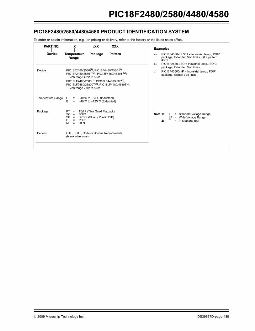
© 2009 Microchip Technology Inc. DS39637D-page 489
PIC18F2480/2580/4480/4580
PIC18F2480/2580/4480/4580 PRODUCT IDENTIFICATION SYSTEMTo order or obtain information, e.g., on pricing or delivery, refer to the factory or the listed sales office.
PART NO. X /XX XXX
PatternPackageTemperatureRange
Device
Device PIC18F2480/2580(1), PIC18F4480/4580 (1),
PIC18F2480/2580T (2), PIC18F4480/4580T (2); VDD range 4.2V to 5.5VPIC18LF2480/2580(1), PIC18LF4480/4580(1), PIC18LF2480/25800T(2), PIC18LF4480/4580T(2); VDD range 2.0V to 5.5V
Temperature Range I = -40°C to +85°C (Industrial)E = -40°C to +125°C (Extended)
Package PT = TQFP (Thin Quad Flatpack)SO = SOICSP = SPDIP (Skinny Plastic DIP)P = PDIPML = QFN
Pattern QTP, SQTP, Code or Special Requirements (blank otherwise)
Examples:a) PIC18F4580-I/P 301 = Industrial temp., PDIP
package, Extended VDD limits, QTP pattern #301.
b) PIC18F2580-I/SO = Industrial temp., SOIC package, Extended VDD limits.
c) PIC18F45805-I/P = Industrial temp., PDIP package, normal VDD limits.
Note 1: F = Standard Voltage RangeLF = Wide Voltage Range
2: T = in tape and reel

DS39637D-page 490 © 2009 Microchip Technology Inc.
AMERICASCorporate Office2355 West Chandler Blvd.Chandler, AZ 85224-6199Tel: 480-792-7200 Fax: 480-792-7277Technical Support: http://support.microchip.comWeb Address: www.microchip.comAtlantaDuluth, GA Tel: 678-957-9614 Fax: 678-957-1455BostonWestborough, MA Tel: 774-760-0087 Fax: 774-760-0088ChicagoItasca, IL Tel: 630-285-0071 Fax: 630-285-0075ClevelandIndependence, OH Tel: 216-447-0464 Fax: 216-447-0643DallasAddison, TX Tel: 972-818-7423 Fax: 972-818-2924DetroitFarmington Hills, MI Tel: 248-538-2250Fax: 248-538-2260KokomoKokomo, IN Tel: 765-864-8360Fax: 765-864-8387Los AngelesMission Viejo, CA Tel: 949-462-9523 Fax: 949-462-9608Santa ClaraSanta Clara, CA Tel: 408-961-6444Fax: 408-961-6445TorontoMississauga, Ontario, CanadaTel: 905-673-0699 Fax: 905-673-6509
ASIA/PACIFICAsia Pacific OfficeSuites 3707-14, 37th FloorTower 6, The GatewayHarbour City, KowloonHong KongTel: 852-2401-1200Fax: 852-2401-3431Australia - SydneyTel: 61-2-9868-6733Fax: 61-2-9868-6755China - BeijingTel: 86-10-8528-2100 Fax: 86-10-8528-2104China - ChengduTel: 86-28-8665-5511Fax: 86-28-8665-7889China - Hong Kong SARTel: 852-2401-1200 Fax: 852-2401-3431China - NanjingTel: 86-25-8473-2460Fax: 86-25-8473-2470China - QingdaoTel: 86-532-8502-7355Fax: 86-532-8502-7205China - ShanghaiTel: 86-21-5407-5533 Fax: 86-21-5407-5066China - ShenyangTel: 86-24-2334-2829Fax: 86-24-2334-2393China - ShenzhenTel: 86-755-8203-2660 Fax: 86-755-8203-1760China - WuhanTel: 86-27-5980-5300Fax: 86-27-5980-5118China - XiamenTel: 86-592-2388138 Fax: 86-592-2388130China - XianTel: 86-29-8833-7252Fax: 86-29-8833-7256China - ZhuhaiTel: 86-756-3210040 Fax: 86-756-3210049
ASIA/PACIFICIndia - BangaloreTel: 91-80-3090-4444 Fax: 91-80-3090-4080India - New DelhiTel: 91-11-4160-8631Fax: 91-11-4160-8632India - PuneTel: 91-20-2566-1512Fax: 91-20-2566-1513Japan - YokohamaTel: 81-45-471- 6166 Fax: 81-45-471-6122Korea - DaeguTel: 82-53-744-4301Fax: 82-53-744-4302Korea - SeoulTel: 82-2-554-7200Fax: 82-2-558-5932 or 82-2-558-5934Malaysia - Kuala LumpurTel: 60-3-6201-9857Fax: 60-3-6201-9859Malaysia - PenangTel: 60-4-227-8870Fax: 60-4-227-4068Philippines - ManilaTel: 63-2-634-9065Fax: 63-2-634-9069SingaporeTel: 65-6334-8870Fax: 65-6334-8850Taiwan - Hsin ChuTel: 886-3-6578-300Fax: 886-3-6578-370Taiwan - KaohsiungTel: 886-7-536-4818Fax: 886-7-536-4803Taiwan - TaipeiTel: 886-2-2500-6610 Fax: 886-2-2508-0102Thailand - BangkokTel: 66-2-694-1351Fax: 66-2-694-1350
EUROPEAustria - WelsTel: 43-7242-2244-39Fax: 43-7242-2244-393Denmark - CopenhagenTel: 45-4450-2828 Fax: 45-4485-2829France - ParisTel: 33-1-69-53-63-20 Fax: 33-1-69-30-90-79Germany - MunichTel: 49-89-627-144-0 Fax: 49-89-627-144-44Italy - Milan Tel: 39-0331-742611 Fax: 39-0331-466781Netherlands - DrunenTel: 31-416-690399 Fax: 31-416-690340Spain - MadridTel: 34-91-708-08-90Fax: 34-91-708-08-91UK - WokinghamTel: 44-118-921-5869Fax: 44-118-921-5820
WORLDWIDE SALES AND SERVICE
03/26/09