picmg exp.0 r.93 specification - norco technologies · pdf filepicmg exp.0 r.93 specification...
TRANSCRIPT

PICMG EXP.0 R.93 SpecificationDraft
March 11, 2005
DRAFT SPECIFICATION FOR REVIEW ONLY
DO NOT DESIGN TO/DO NOT CLAIM COMPLIANCE TO/DO NOT DISTRIBUTE THIS SPECIFICATION

©Copyright 2005, PCI Industrial Computer Manufacturers Group.
The attention of adopters is directed to the possibility that compliance with or adoption of PICMG® specifications may require use of an invention covered by patent rights. PICMG® shall not be responsible for identifying patents for which a license may be required by any PICMG® specification or for conducting legal inquiries into the legal validity or scope of those patents that are brought to its attention. PICMG® specifications are prospective and advisory only. Prospective users are responsible for protecting themselves against liability for infringement of patents.
NOTICE:
The information contained in this document is subject to change without notice. The material in this document details a PICMG® specification in accordance with the license and notices set forth on this page. This document does not represent a commitment to implement any portion of this specification in any company's products.
WHILE THE INFORMATION IN THIS PUBLICATION IS BELIEVED TO BE ACCURATE, PICMG® MAKES NO WARRANTY OF ANY KIND, EXPRESS OR IMPLIED, WITH REGARD TO THIS MATERIAL INCLUDING, BUT NOT LIMITED TO, ANY WARRANTY OF TITLE OR OWNERSHIP, IMPLIED WARRANTY OF MERCHANTABILITY OR WARRANTY OF FITNESS FOR PARTICULAR PURPOSE OR USE.
In no event shall PICMG® be liable for errors contained herein or for indirect, incidental, special, consequential, reliance or cover damages, including loss of profits, revenue, data or use, incurred by any user or any third party.
Compliance with this specification does not absolve manufacturers of CompactPCI Express™ equipment from the requirements of safety and regulatory agencies (UL, CSA, FCC, IEC, etc.).
The PICMG® and CompactPCI® names and the PICMG®, CompactPCI®, and CompactPCI Express® logos are registered trademarks of the PCI Industrial Computer Manufacturers Group.
All other brand or product names may be trademarks or registered trademarks of their respective holders.
PICMG EXP.O CompactPCI Express Specification, Draft R.93, March 11, 2005Do Not Design To/Do Not Claim Compliance To/Do Not Distribute This Specification

Contents1 Introduction ..........................................................................................................13
1.1 Statement of Compliance ............................................................................131.2 Terminology.................................................................................................131.3 Applicable Documents.................................................................................181.4 Objectives....................................................................................................191.5 Name and Logo Usage ...............................................................................20
1.5.1 Logo Use ........................................................................................201.5.2 Trademark Policy ...........................................................................20
1.6 Intellectual Property.....................................................................................211.7 Special Word Usage....................................................................................221.8 Connectors ..................................................................................................22
1.8.1 Legacy CompactPCI Connectors ...................................................221.8.2 High-Speed Advanced Differential Fabric Connectors ...................231.8.3 UPM Power Connectors .................................................................25
1.8.3.1 System Slot/Board and Type 1 Peripheral Slot/Board....251.8.3.2 Switch Slot/Board ...........................................................26
1.8.4 eHM Connector ..............................................................................271.8.5 CompactPCI Pluggable Power Supply Connector .........................27
1.9 Slot and Board Descriptions........................................................................281.9.1 Connector Reference Designators .................................................311.9.2 System Slot and Board...................................................................311.9.3 Type 1 Peripheral Slot and Board ..................................................321.9.4 Type 2 Peripheral Slot and Board ..................................................331.9.5 Hybrid Peripheral Slot ....................................................................351.9.6 Legacy Slot.....................................................................................361.9.7 Switch Slot and Board ....................................................................36
1.9.7.1 3U Switch Slot and Board...............................................361.9.7.2 6U Switch Slot and Board...............................................37
1.10 Example Configurations ..............................................................................40
2 Mechanical Requirements ..................................................................................452.1 Mechanical Overview ..................................................................................452.2 Drawing Standard........................................................................................452.3 Units ............................................................................................................452.4 Keepout Zones ............................................................................................452.5 Connector Requirements ............................................................................45
2.5.1 ADF Connectors .............................................................................452.5.1.1 Board Connectors...........................................................452.5.1.2 Backplane Connectors without Hot-Plug Support ..........462.5.1.3 Backplane Connectors with Hot-Plug Support ...............46
2.5.2 eHM Connectors ............................................................................462.5.2.1 Board Connector Type Designation ...............................462.5.2.2 Backplane Connectors without Hot-Plug Support ..........462.5.2.3 Backplane Connectors with Hot-Plug Support ...............46
2.5.3 UPM Connectors ............................................................................462.5.3.1 Backplane Connectors ...................................................462.5.3.2 Board Connectors without Hot-Plug Support..................47
PICMG EXP.O CompactPCI Express Specification, Draft R.93, March 11, 2005 3Do Not Design To/Do Not Claim Compliance To/Do Not Distribute This Specification

2.5.3.3 Board Connectors with Hot-Plug Support....................... 472.5.4 HM Connectors .............................................................................. 472.5.5 47-Position Pluggable Power Supply Connector............................ 47
2.6 Chassis Subrack Requirements .................................................................. 472.7 Backplane Requirements ............................................................................ 47
2.7.1 3U Backplane Dimensions and Connector Locations .................... 472.7.2 6U Backplane Dimensions and Connector Locations .................... 49
2.8 Slot Numbering and Glyphs ........................................................................ 512.9 Board Requirements ................................................................................... 51
2.9.1 3U System/Type 1/Type 2 Board Dimensions and Connector Locations ........................................................................................ 51
2.9.2 6U System/Type 1/Type 2 Board Dimensions and Connector Locations ........................................................................................ 53
2.9.3 3U Switch Board Dimensions and Connector Locations................ 542.9.4 6U Switch Board Dimensions and Connector Locations................ 552.9.5 Board PCB Thickness .................................................................... 562.9.6 ESD Discharge Strip ...................................................................... 562.9.7 ESD Clip......................................................................................... 562.9.8 Front Panels ................................................................................... 562.9.9 CompactPCI Express Logo ............................................................ 572.9.10 PMC/XMC Support......................................................................... 572.9.11 Cross Sectional View ..................................................................... 582.9.12 Component Outline and Warpage.................................................. 582.9.13 Solder Side Cover (Optional) ......................................................... 582.9.14 Component Heights........................................................................ 592.9.15 System Slot Identification ............................................................... 59
2.10 Rear-Panel I/O Board Requirements .......................................................... 592.10.1 3U Rear-Panel I/O Board Dimensions ........................................... 592.10.2 6U Rear-Panel I/O Board Dimensions ........................................... 60
3 Electrical Requirements ...................................................................................... 623.1 Signal Definitions......................................................................................... 62
3.1.1 PCI Express Signals....................................................................... 623.1.1.1 PCI Express Transmit Signals........................................ 623.1.1.2 PCI Express Receive Signals......................................... 623.1.1.3 Interconnect Definition.................................................... 63
3.1.1.3.1 Link Definition .............................................. 633.1.1.3.2 Link Grouping .............................................. 63
3.1.1.4 Electrical Budgets........................................................... 643.1.1.4.1 AC Coupling................................................. 653.1.1.4.2 Insertion Loss .............................................. 653.1.1.4.3 Crosstalk...................................................... 663.1.1.4.4 Lane-to-Lane Skew...................................... 673.1.1.4.5 Equalization ................................................. 673.1.1.4.6 Skew within the Differential Pair (Intra-Pair
Skew)........................................................... 673.1.1.5 Jitter Budget Allocation................................................... 68
3.1.1.5.1 Random Jitter (Rj)........................................ 683.1.1.5.2 System Level Jitter Distribution ................... 693.1.1.5.3 Interconnect Jitter Budget............................ 693.1.1.5.4 Eye Patterns ................................................ 703.1.1.5.5 Type 2 Peripheral Transmitter Eye .............. 71
4 PICMG EXP.O CompactPCI Express Specification, Draft R.93, March 11, 2005Do Not Design To/Do Not Claim Compliance To/Do Not Distribute This Specification

3.1.1.5.6 Controller Transmitter Eye ...........................723.1.1.5.7 Type 2 Peripheral Receiver Eye ..................733.1.1.5.8 Controller Receiver Eye ...............................743.1.1.5.9 Backplane Compliance Testing ...................753.1.1.5.10 Alternative Controller TX Measurement.......77
3.1.1.6 Reference Clock .............................................................783.1.1.6.1 Hot-Plug .......................................................783.1.1.6.2 Clock Fan-Out..............................................793.1.1.6.3 Clocking Dependencies ...............................793.1.1.6.4 AC-Coupling and Biasing.............................793.1.1.6.5 Routing Length.............................................803.1.1.6.6 Reference Clock Specification .....................813.1.1.6.7 REFCLK Phase Jitter Specification .............84
3.1.2 ESD ................................................................................................853.1.3 5 Vaux ............................................................................................853.1.4 SMBus............................................................................................85
3.1.4.1 SMBus “Back Powering” Considerations........................883.1.4.2 Backplane Identification and Capability Using SMBus ...88
3.1.5 PWRBTN# Signal ...........................................................................943.1.6 PS_ON# Signal ..............................................................................943.1.7 PWR_OK Signal .............................................................................953.1.8 WAKE# Signal ................................................................................96
3.1.8.1 Implementation Note ......................................................983.1.9 PERST# Signal ..............................................................................99
3.1.9.1 Initial Power-Up (G3 to L0) ...........................................1003.1.9.2 Power Management States (S0 to S3/S4 to S0) ..........1013.1.9.3 Power Down .................................................................102
3.1.10 SYSEN# Signal ............................................................................1033.1.11 Geographical Addressing .............................................................1033.1.12 LINKCAP Signal ...........................................................................1043.1.13 I/O Pins.........................................................................................1043.1.14 Reserved Pins ..............................................................................104
3.2 Hot-Plug Support.......................................................................................1043.2.1 Hot-Plug Sub-System Architecture...............................................1043.2.2 Power Enable ...............................................................................1073.2.3 Wake# ..........................................................................................1083.2.4 Module Power Good.....................................................................1083.2.5 Present Detection.........................................................................1083.2.6 System Management Bus ............................................................1083.2.7 System Management Bus Alert ....................................................1083.2.8 Attention LED ...............................................................................1093.2.9 Attention Switch............................................................................1093.2.10 DC Specifications .........................................................................109
3.3 Backplane Connector Pin Assignments ....................................................1093.3.1 System Slot ..................................................................................109
3.3.1.1 4-Link Configuration .....................................................1103.3.1.2 2-Link Combination Configuration ................................111
3.3.2 Peripheral Slot Type 1..................................................................1133.3.3 Peripheral Slot Type 2..................................................................1153.3.4 Hybrid Peripheral Slot ..................................................................1153.3.5 Legacy Slot...................................................................................117
PICMG EXP.O CompactPCI Express Specification, Draft R.93, March 11, 2005 5Do Not Design To/Do Not Claim Compliance To/Do Not Distribute This Specification

3.3.6 Switch Slot.................................................................................... 1173.3.6.1 3U Switch Slot .............................................................. 1173.3.6.2 6U Switch Slot—x4 Link Width ..................................... 1183.3.6.3 6U Switch Slot—x8 Link Width ..................................... 121
3.4 Power Supply Requirements..................................................................... 1233.4.1 Current Available.......................................................................... 1233.4.2 Regulation and Ripple and Noise................................................. 1243.4.3 Backplane Power Decoupling ...................................................... 1243.4.4 Power Supply Timing ................................................................... 1243.4.5 Additional Power Requirements for Boards Supporting
Hot-Plug ....................................................................................... 125
4 Keying Requirements ........................................................................................ 1264.1 Legacy Slots and Legacy Boards.............................................................. 1264.2 eHM Keying............................................................................................... 126
A CompactPCI Express Advanced Differential Fabric Connector .................... 129A.1 General Data ............................................................................................. 129
A.1.1 Objective of this Document ......................................................... 129A.1.2 Scope ........................................................................................... 129A.1.3 Intended Method of Mounting....................................................... 129A.1.4 Ratings and Characteristics ......................................................... 130A.1.5 Normative References.................................................................. 130A.1.6 Markings....................................................................................... 131A.1.7 Type Designation ......................................................................... 131A.1.8 Ordering Information .................................................................... 132A.1.9 Special Connector Loadings ........................................................ 132
A.2 Technical Information ................................................................................ 133A.2.1 Contacts and Terminations .......................................................... 133
A.3 Dimensional Information............................................................................ 134A.3.1 Isometric View and Common Features ........................................ 134A.3.2 Engagement Information .............................................................. 134
A.3.2.1 Electrical Engagement Length...................................... 134A.3.2.2 First Contact Point ........................................................ 135A.3.2.3 Perpendicular to Engagement Direction....................... 135A.3.2.4 Inclination ..................................................................... 135
A.3.3 Backplane Connectors ................................................................. 136A.3.3.1 Dimensions................................................................... 136A.3.3.2 Contacts ....................................................................... 136A.3.3.3 Contact Tip Geometry .................................................. 137A.3.3.4 Terminations................................................................. 137
A.3.4 Front Board Connectors ............................................................... 138A.3.4.1 Dimensions................................................................... 138A.3.4.2 Terminations................................................................. 138
A.3.5 Mounting Information for Backplane Connectors ......................... 138A.3.5.1 Hole Pattern on Backplanes ......................................... 139A.3.5.2 Backplane Contact Positional Requirements ............... 139A.3.5.3 True Position of Male Contacts .................................... 139
A.3.6 Mounting Information for Front Board Connectors ....................... 140A.3.6.1 Hole Pattern on Printed Boards.................................... 140
A.4 Characteristics........................................................................................... 141
6 PICMG EXP.O CompactPCI Express Specification, Draft R.93, March 11, 2005Do Not Design To/Do Not Claim Compliance To/Do Not Distribute This Specification

A.4.1 Climatic Category .........................................................................141A.4.1.1 Climatic Category Test batch P: Initial Examination.....141A.4.1.2 Climatic Category Test Batch A: Mechanical Tests......141A.4.1.3 Climatic Category Test Batch B: Harsh Environments .144A.4.1.4 Climatic Category Test Batch C: Damp Heat ...............146A.4.1.5 Climatic Category Test Batch D: Extended
Environmental Tests.....................................................147A.4.1.6 Climatic Category Test Batch E: Extended
Environmental Tests.....................................................148A.4.2 Electrical Characteristics ..............................................................148
A.4.2.1 Impedance....................................................................148A.4.2.2 Crosstalk.......................................................................149A.4.2.3 Propagation Delay ........................................................149A.4.2.4 Differential Skew...........................................................149A.4.2.5 Insertion Loss ...............................................................149
B Enriched Hard-Metric Connector ......................................................................150B.1 General Data .............................................................................................150
B.1.1 Objective of this Document ..........................................................150B.1.2 Description of the Connector’s Approach.....................................150B.1.3 Descriptive Partitions Found Further This Document...................150B.1.4 Normative References..................................................................151
B.1.4.1 Primary References Describing the Generic Part of the Connector ...............................................................151
B.1.4.2 Additional References ..................................................151B.1.5 Intended Method of Mounting.......................................................151B.1.6 Markings.......................................................................................152B.1.7 Type Designation (General) .........................................................152
B.2 Technical Information ................................................................................152B.2.1 Definitions.....................................................................................152B.2.2 Contacts .......................................................................................152B.2.3 Contact Performance Level ..........................................................154B.2.4 Keying ..........................................................................................154
B.2.4.1 Mating Rules.................................................................155B.2.4.2 Examples for Mating and Nonmating Configurations ...156
B.2.5 Type Designation .........................................................................156B.2.6 Applicational Information ..............................................................157
B.2.6.1 Alignment and Gathering..............................................157B.2.6.2 Polarization...................................................................158
B.3 Dimensional Information............................................................................158B.3.1 General.........................................................................................158B.3.2 View and Common Features........................................................158B.3.3 Remarks on Mating Properties of eHM Connector.......................159B.3.4 Fixed Board Connector ................................................................160
B.3.4.1 Dimensions...................................................................160B.3.4.2 Terminations.................................................................161B.3.4.3 Mounting Information for Fixed Board Connectors.......161B.3.4.4 Hole Pattern on Fixed Board ........................................161B.3.4.5 Position of Connectors on Fixed Board ........................161
B.3.5 Free Board Connectors ................................................................162B.3.5.1 Dimensions...................................................................162B.3.5.2 Terminations.................................................................163
PICMG EXP.O CompactPCI Express Specification, Draft R.93, March 11, 2005 7Do Not Design To/Do Not Claim Compliance To/Do Not Distribute This Specification

B.3.5.3 Mounting Information for Free Board Connectors ........ 163B.3.5.4 Hole Pattern on Free Board.......................................... 163B.3.5.5 Position of Connectors on Front Board ........................ 163
B.4 Characteristics........................................................................................... 163B.4.1 Climatic Category ......................................................................... 163B.4.2 Electrical Characteristics .............................................................. 163
B.4.2.1 Creepage and Clearance Distances............................. 163B.4.2.2 Voltage Proof................................................................ 164B.4.2.3 Current-Carrying Capacity............................................ 164B.4.2.4 Contact Resistance ...................................................... 164B.4.2.5 Insulation Resistance ................................................... 164
B.4.3 Mechanical ................................................................................... 164B.4.3.1 Mechanical Operation................................................... 164B.4.3.2 Engaging and Separating Forces ................................. 164B.4.3.3 Contact Retention in Insert ........................................... 164B.4.3.4 Static Load, Transverse................................................ 164B.4.3.5 Gauge Retention Force ................................................ 164B.4.3.6 Vibration (Sinusoidal) ................................................... 164B.4.3.7 Shock............................................................................ 164B.4.3.8 Polarization Method...................................................... 165B.4.3.9 Robustness and Effectiveness of Coding Device......... 165
B.4.3.9.1 Conditions According to IEC60512-7, Test 13e..................................................... 165
B.5 Test Schedule ........................................................................................... 165B.6 Quality Assessment Procedures ............................................................... 165
C Universal Power Connector (UPM)................................................................... 166C.1 General Data ............................................................................................. 166
C.1.1 Objective of this Document .......................................................... 166C.2 Dimensions................................................................................................ 167C.3 Perpendicular to Engagement Direction.................................................... 169C.4 Inclination .................................................................................................. 169C.5 Mounting Information................................................................................. 169C.6 Climatic Category ...................................................................................... 171
Figures1-1 HM Connectors ................................................................................................ 231-2 Advanced Differential Fabric (ADF) Connector ................................................ 241-3 UPM Power Connector for System and Type 1 Peripheral Slots/Boards......... 251-4 Power Connector for Switch Slots/Boards ....................................................... 261-5 eHM Connector ................................................................................................ 271-6 47-Position CompactPCI Pluggable Power Supply Connector ........................ 281-7 CompactPCI Express 3U Slot Examples ......................................................... 291-8 CompactPCI Express 6U Slot Examples ......................................................... 301-9 System Board................................................................................................... 311-10 System Slot ...................................................................................................... 321-11 Type 1 Peripheral Board .................................................................................. 321-12 Type 1 Peripheral Slot ...................................................................................... 331-13 Type 2 Peripheral Board .................................................................................. 341-14 Type 2 Peripheral Slot ...................................................................................... 34
8 PICMG EXP.O CompactPCI Express Specification, Draft R.93, March 11, 2005Do Not Design To/Do Not Claim Compliance To/Do Not Distribute This Specification

1-15 Hybrid Peripheral Slot.......................................................................................351-16 Boards Supported By Hybrid Peripheral Slots..................................................361-17 3U Switch Board...............................................................................................371-18 3U Switch Slot ..................................................................................................371-19 6U Switch Board...............................................................................................381-20 6U Switch Slot ..................................................................................................391-21 Backplane with Hybrid Peripheral Slots and Legacy Slots ...............................401-22 Backplane with all Hybrid Peripheral Slots .......................................................411-23 Backplane with Type 2 and Hybrid Peripheral Slots.........................................421-24 3U Backplane with Switch, System, Type 1, and Type 2 Slots ........................431-25 6U Backplane with Switch, System, Type 1, and Type 2 Slots ........................442-1 Backplane Overall Dimensions.........................................................................482-2 3U Backplane Connector Locations .................................................................492-3 6U Backplane Connector Locations .................................................................502-4 Board Compatibility Glyphs ..............................................................................512-5 Glyph for Boards that Operate in Either System or Peripheral Slots................512-6 Slot Compatibility Glyphs..................................................................................512-7 3U System, Type 1, and Type 2 Board Dimensions and Connector
Locations ..........................................................................................................522-8 6U System/Type 1/Type 2 Board Dimensions and Connector Locations.........532-9 3U Switch Board Dimensions and Connector Locations ..................................542-10 6U Switch Board Dimensions and Connector Locations ..................................552-11 Modification to PCB to Support Thicker Boards ...............................................562-12 CompactPCI Express Logo ..............................................................................572-13 Alternate CompactPCI Express Logo...............................................................572-14 Approximate Clearance Between the PMC/XMC PCB and the ADF
Connector.........................................................................................................572-15 Board Cross-Sectional View.............................................................................582-16 3U Rear-Panel I/O Board Dimensions..............................................................602-17 6U Rear-Panel I/O Board Dimensions..............................................................613-1 2-Link and Loss Definition ................................................................................643-2 Backplane Connector Footprint ........................................................................683-3 Interconnect Jitter Allocation ............................................................................703-4 Peripheral TX Eye Mask...................................................................................723-5 Controller TX Eye Mask....................................................................................733-6 Peripheral RX Eye Mask ..................................................................................743-7 Controller RX Eye Mask ...................................................................................753-8 Backplane TX Compliance Signal ....................................................................763-9 Backplane RX Eye............................................................................................763-10 Alternative Controller Measurement .................................................................783-11 Biasing for HCSL Clock Input ...........................................................................803-12 Biasing Simulation Results ...............................................................................803-13 Single-Ended Measurement for Swing .............................................................833-14 Single-Ended Measurement Points for Delta Cross Point................................833-15 Single-Ended Measurement Points for Rise and Fall Time Matching ..............833-16 Differential Measurement Points for Duty Cycle and Period ............................833-17 Differential Measurement Points for Rise and Fall Time ..................................843-18 Differential Measurement Points for Ringback .................................................843-19 Eight-Slot Backplane Example .........................................................................913-20 Power Supply Timing........................................................................................95
PICMG EXP.O CompactPCI Express Specification, Draft R.93, March 11, 2005 9Do Not Design To/Do Not Claim Compliance To/Do Not Distribute This Specification

3-21 WAKE Rise and Fall Time Measurement Points .............................................. 983-22 WAKE# Circuit Example................................................................................... 993-23 Power Up........................................................................................................ 1013-24 Power Management States ............................................................................ 1023-25 Power Down ................................................................................................... 1033-26 Typical Hot-Plug Interface Implementation .................................................... 1063-27 4-Link Configuration Backplane Example ...................................................... 1103-28 2-Link Combination Configuration Backplane Example ................................. 112A-1 Sample Part Number with Explanation........................................................... 132A-2 Special Connector Loading 0100 ................................................................... 133A-3 View of Connectors with Common Features .................................................. 134A-4 Connector Mating Sequence.......................................................................... 135A-5 Dimensional Drawing of Backplane Connector .............................................. 136A-6 Contact Geometry for Zone 2 Backplane Connector ..................................... 137A-7 Dimensional Drawing of Front Board Connectors .......................................... 138A-8 Hole Requirements for Backplane Connector ................................................ 139A-9 Backplane Pin Contact Positional Tolerance ................................................. 140A-10 Hole Requirements for the Front Board Connector ........................................ 140B-1 View of Fixed and Free Board Keying Design (Left Perspective, Right
Detailed) ......................................................................................................... 155B-2 View of a Mating and a Non-Mating Keying Combination .............................. 156B-3 View of Fixed and Free Board Connectors .................................................... 158B-4 View of Fixed Board Connector Including Polarization Feature ..................... 159B-5 Dimensional Drawing of Fixed Board eHM Connector ................................... 160B-6 Hole Requirements for eHM on Fixed Board ................................................. 161B-7 Dimensional Drawing of eHM Free Board Connector .................................... 162B-8 Hole Requirements for eHM Free Board Connector ...................................... 163C-1 UPM-F-7 Female 7-Position Power Connector Dimensional Information ...... 167C-2 UPM-F-5 Female 5-Position Power Connector Dimensional Information ...... 168C-3 Male 7-Position Power Connector Dimensional Information .......................... 168C-4 UPM-M-5 Male 5-Position Power Connector Dimensional Information.......... 169C-5 Hole Pattern for 7-Row Male UPM Power Connector .................................... 169C-6 Hole Pattern for 5-Row Male UPM Power Connector .................................... 170C-7 Hole Pattern for Female 7-Row UPM Power Connector ................................ 170C-8 Hole Pattern for Female 5-Row UPM Power Connector ................................ 171
Tables3-1 Interconnect Loss Budget Type 1 Peripheral ................................................... 653-2 Interconnect Loss Budget Type 2 Peripheral ................................................... 653-3 Allowable Interconnect Lane-to-Lane Skew ..................................................... 673-4 Total System Jitter Distribution......................................................................... 693-5 Interconnect Jitter Budget ................................................................................ 703-6 Type 2 Peripheral Transmitter Eye................................................................... 713-7 Controller TX Compliance Eye Requirements.................................................. 723-8 Type 2 Peripheral RX Compliance Eye Requirements .................................... 733-9 Controller RX Compliance Eye Requirements ................................................. 743-10 Backplane TX Compliance Signal (Signal Generator) ..................................... 753-11 Backplane RX Compliance Eye ....................................................................... 76
10 PICMG EXP.O CompactPCI Express Specification, Draft R.93, March 11, 2005Do Not Design To/Do Not Claim Compliance To/Do Not Distribute This Specification

3-12 Reference Clock Source AC Timing.................................................................813-13 Maximum Allowed Phase Jitter ........................................................................853-14 Capacitance Budgets for SMBus, ALERT, and WAKE# Signals......................863-15 DC Electrical Requirements for the SMBus......................................................863-16 DC Electrical Requirements for the ALERT# Signal.........................................873-17 Backplane Descriptor .......................................................................................883-18 System Slot Descriptor .....................................................................................893-19 Peripheral Slot Descriptor.................................................................................903-20 Backplane Identification and Capability Record Example ................................923-21 PS_ON# Signal Characteristics........................................................................943-22 PWR_OK Signal Characteristics ......................................................................953-23 DC Electrical Requirements for the WAKE# Signal..........................................973-24 Sequencing and Reset Signal Timings.............................................................983-25 DC Electrical Requirements for the PERST# Signal ......................................1003-26 Signals Involved in Hot-Plug...........................................................................1063-27 Hot-Plug Auxiliary Signal DC Specifications...................................................1093-28 4-Link Configuration System Slot Pin Assignments .......................................1113-29 2-Link Combination Configuration System Slot Pin Assignments ..................1133-30 Peripheral Type 1 Pin Assignments ...............................................................1143-31 Peripheral Slot Type 2 Pin Assignments ........................................................1153-32 Hybrid Peripheral Slot Pin Assignments.........................................................1163-33 3U x4 Switch Slot Pin Assignments................................................................1183-34 6U Switch Slot Pin Assignments for x4 Lane Configuration Part 1 ................1193-35 6U Switch Slot Pin Assignments for x4 Lane Configuration Part 2 ................1203-36 6U Switch Slot Pin Assignments for x8 Lane Configuration Part 1 ................1213-37 6U Switch Slot Pin Assignments for x8 Lane Configuration Part 2 ................1223-38 Maximum Current Available Through Pins .....................................................1233-39 Regulation and Ripple and Noise ...................................................................1243-40 Minimum Power Decoupling Requirements ...................................................1243-41 Board Hot-Plug Capacitance and Current Limits............................................1254-1 Electrical Compatibility Between eHM I/O Pin Uses.......................................1274-2 eHM Male Connector Keying Designators .....................................................1274-3 eHM Female Connector Keying Designators .................................................127A-1 Connector Contact Engagement ....................................................................135A-2 Test Batch P ...................................................................................................141A-3 Test Batch A ...................................................................................................141A-4 Test Batch B ...................................................................................................144A-5 Test Batch C...................................................................................................146A-6 Test Batch D...................................................................................................147A-7 Test Batch E ...................................................................................................148A-8 Electrical Characteristics ................................................................................148A-9 Propagation Delay ..........................................................................................149A-10 Differential Skew.............................................................................................149B-1 Non-Hot-Plug Pin Length Definition................................................................153B-2 Hot-Plug Pin Length Definition .......................................................................153B-3 Pin Level Designation Cross Reference.........................................................154C-1 Climatic Category ...........................................................................................171
PICMG EXP.O CompactPCI Express Specification, Draft R.93, March 11, 2005 11Do Not Design To/Do Not Claim Compliance To/Do Not Distribute This Specification

12 PICMG EXP.0 CompactPCI Express Specification, Draft R.93, March 11, 2005Do Not Design To/Do Not Claim Compliance To/Do Not Distribute This Specification
History
Date Revision Change History

Introduction
Introduction 1
1.1 Statement of ComplianceStatements of compliance with this specification take the form specified in the PICMG® Policies and Procedures for Specification Development:
“This product complies with PICMG® EXP.0 Revision 1.0.”
Products making this simple claim of compliance must provide, at a minimum, all features defined in this specification as being mandatory by the use of the keyword “shall” in the body of the specification. Such products may also provide recommended features associated with the keyword “should” and permitted features associated with the keyword “may” as well.
1.2 TerminologyThe following terms and acronyms are used in specific ways throughout this specification:
Term Definition
8b/10b The data encoding scheme used in the PCI Express Version 1.1 Physical Layer.
ACPI Acronym for Advanced Configuration and Power Interface.
Asserted A signal is Asserted when it is in the state the signal name indicates. Opposite of Negated.
Auxiliary Signals Signals not required by the PCI Express architecture but necessary for certain desired Functions or system implementation. For example, the REFCLK signal.
Backplane A circuit board assembly typically mounted in a Subrack that provides the connectors signals, power, ground, etc., that allow boards defined in this specification to operate.
Backplane Capability Record The data stored in the Backplane EPROM that describes the type of slot and the bandwidth for each Backplane slot.
Backplane Descriptor The part of the Backplane Capability Record that includes the Backplane manufacturer, model, revision, serial number, and slot count.
Beacon An Optional 30 kHz–500 MHz in-band signal used to exit the L2 Link Power Management state. One of two defined mechanisms for waking up a Link in L2 (see also Wakeup).
BIOS Acronym for Basic Input/Output System. When BIOS is in Read-Only Memory Devices, it may be referred to as ROM BIOS.
Board A generic reference to all the board types defined in this specification.
Bridge A Device that virtually or actually connects a PCI/PCI-X segment or PCI Express Port with an internal Component interconnect or with another PCI/PCI-X segment or PCI Express Port. A virtual Bridge in a Root Complex or Switch must use the software configuration interface described in the PCI Express Base Specification.
PICMG EXP.0 CompactPCI Express Specification, Draft R.93, March 11, 2005 13Do Not Design To/Do Not Claim Compliance To/Do Not Distribute This Specification

Introduction
by-1, x1 A Link or Port with one Physical Lane.
by-4, x4 A Link or Port with four Physical Lanes.
by-8, x8 A Link or Port with eight Physical Lanes.
by-N, xN A Link with “N” Physical Lanes.
Card Guide See Guide Rail.
Character An 8-bit quantity treated as an atomic entity; a byte.
Chassis A Chassis is comprised of at least a Backplane, Subrack, power supply, metal enclosure, and cooling mechanism.
Completer The Logical Device addressed by a Request.
Completion A Packet used to terminate, or to partially terminate, a Transaction Sequence. A Completion always corresponds to a preceding Request, and, in some cases, includes data.
Component A physical Device (a single package).
Configuration Space One of the four address spaces within the PCI Express architecture. Packets with a Configuration Space address are used to configure a Device.
Data Link Layer The intermediate Layer between the Transaction Layer and Physical Layer.
Data Link Layer Packet, DLLP A Packet generated in the Data Link Layer to support Link management Functions.
Data Payload Information following the Header in some Packets destined for consumption by the Logical Device receiving the Packet (for example, Write Requests or Read Completions).
Deasserted The inactive logical state of a conceptual or actual signal.
Device A Logical Device, corresponding to a PCI Device Configuration Space. May be either a single or multifunction Device.
Downstream 1. The relative position of an interconnect/System Element (Port/Component) that is farther from the Root Complex. The Ports on a Switch that are not the Upstream Port are Downstream Ports. All Ports on a Root Complex are Downstream Ports. The Downstream Component on a Link is the Component farther from the Root Complex.2. A direction of information flow where the information is flowing away from the Root Complex.
DWORD, DW Four bytes. Used in the context of a Data Payload, the 4 bytes of data must be on a Naturally Aligned four-byte boundary (the least significant two bits of the byte address are 00b).
Electrical Idle The state of the output driver in which both lines, D+ and D–, are driven to the DC common mode voltage.
Endpoint A Device with a Type 00h Configuration Space Header.
FEXT Far End Crosstalk.
Flow Control The method for communicating receive buffer status from a Receiver to a Transmitter to prevent receive buffer overflow and allow Transmitter compliance with ordering rules.
Function A logical Function corresponding to a PCI Function Configuration Space. May refer to one Function of a multifunction Device, or to the only Function in a single-function Device.
Term Definition
14 PICMG EXP.0 CompactPCI Express Specification, Draft R.93, March 11, 2005Do Not Design To/Do Not Claim Compliance To/Do Not Distribute This Specification

Introduction
Geographical Addressing A mechanism by which a board can determine which Physical Slot it is plugged into within a Chassis.
Guide Rail Slotted rails within the Subrack used to guide the board as it is plugged into and removed from the Backplane. Also known as Card Guides.
Header A set of fields that appear at the front of a Packet that contain the information required to determine the characteristics and purpose of the Packet.
Hierarchy The tree-structured PCI Express I/O interconnect topology.
Host Bridge The part of a Root Complex that connects a host CPU or CPUs to a Hierarchy.
Host System The compute entity that contains the PCI Express Root Complex and is the source of the reference clock signal.
Hot-Plug Insertion and/or removal of a Device, either direct or through a cable, into an active Host or subsystem.
Hybrid Peripheral Slot A slot that supports either a Type 2 Peripheral Board, a 32-bit CompactPCI Board, or a PXI Board with the eHM connector populated instead of the J2 connector.
In-Band Signaling A method for signaling events and conditions using the Link between two Components, as opposed to the use of separate physical (sideband) signals. All PCI Express-defined mechanisms can be implemented using In-Band Signaling, although in some form factors, Sideband Signaling may be specified instead.
I/O An abbreviation for Input/Output.
IPMI Intelligent Platform Management Interface. A specification and mechanism for providing inventory management, monitoring, logging, and control for elements of a computer system. As defined in the Intelligent Platform Management Interface Specification.
ISI Inter-Symbol Interference.
Isochronous Data associated with time-sensitive applications, such as audio or video applications.
Lane A set of differential signal pairs, one pair for transmission and one pair for reception. A by-N Link is composed of N Lanes.
Layer A unit of distinction applied to this specification to help clarify the behavior of key elements. The use of the term Layer does not imply a specific implementation.
Legacy Board A board defined in the PICMG 2.0 (CompactPCI) specification.
Legacy Slot A slot defined in the PICMG 2.0 (CompactPCI) specification.
Link The collection of two Ports and their interconnecting Lanes. A Link is a dual simplex communications path between two Components.
Logical Device An element of a PCI Express system that responds to a unique Device number in Configuration Space. Logical Devices are either single-function or multifunction Devices. Logical Device requirements apply to both single-function Logical Devices and each Function individually of a multifunction Logical Device.
Logical Slot A term that applies only to Legacy Peripheral Slots and Hybrid Peripheral Slots. A slot’s Logical Slot number is defined in the PICMG 2.0 (CompactPCI) specification based on which PCI address line is wired to the slot’s IDSEL line.
NEXT Near End Crosstalk.
Term Definition
PICMG EXP.0 CompactPCI Express Specification, Draft R.93, March 11, 2005 15Do Not Design To/Do Not Claim Compliance To/Do Not Distribute This Specification

Introduction
Naturally Aligned A Data Payload with a starting address equal to an integer multiple of a power of two, usually a specific power of two. For example, 64-byte Naturally Aligned means the least significant 6 bits of the byte address are 00 0000b.
Negated A signal is Negated when it is in the state opposed to that which the signal name indicates.
Operating System Software on a Host System that manages resources and provides services, including Power Management services, Device drivers, user mode services, and/or kernel mode services.
Optional A characteristic or feature that is not mandatory, but is specifically permitted. If an Optional characteristic or feature is present, it must be implemented as described in the appropriate specification.
Packet A fundamental unit of information transfer consisting of a Header that, in some cases, is followed by a Data Payload.
PCB Printed Circuit Board. Also referred to as Printed Wiring Board (PWB).
PCI Acronym for the Peripheral Component Interface bus.
PCI Express A scalable full-simplex serial bus standard that operates at 2.5 Gbps and offers both asynchronous and Isochronous data transfers.
PCI-SIG Acronym for PCI Special Interest Group.
Peripheral Board A generic reference to all Peripheral Board types this specification defines.
Peripheral Slot A generic reference to all the Peripheral Slot types this specification defines.
Peripheral Slot Descriptor The portion of the Backplane Capability Record specific to Peripheral Slots.
Physical Lane See Lane.
Physical Layer The Layer that directly interacts with the communication medium between two Components.
Physical Slot The slots that boards can physically plug into that are consecutively numbered on the Chassis and Backplane.
Port Logically, an interface between a Component and a PCI Express Link. Physically, a group of Transmitters and Receivers on the same chip that define a Link.
PPM Parts per Million. Applied to frequency, the difference, in millionths of a Hertz, between a stated ideal frequency and the measured long-term average of a frequency.
Power Management Mechanisms in software and hardware to minimize system power consumption, manage system thermal limits, and maximize system battery life. Power Management involves tradeoffs among system speed, noise, battery life, and AC power consumption.
Pull-Ups Resistors that ensure that signals maintain stable values when no agent is actively driving the bus or signal.
PXI The PXI standard maintained by the PXI Systems Alliance.
Rear I/O Signals routed by a board that pass through the Backplane. These signals are not routed on the Backplane, but pass through on Backplane connector pins.
Receiver The Component that receives Packet information across a Link.
Term Definition
16 PICMG EXP.0 CompactPCI Express Specification, Draft R.93, March 11, 2005Do Not Design To/Do Not Claim Compliance To/Do Not Distribute This Specification

Introduction
Request A Packet that initiates a Transaction Sequence. A Request includes operation code and, in some cases, address and length, data, or other information.
Requester A Logical Device that first introduces a Transaction Sequence into the PCI Express domain.
Root Complex An entity that includes a Host Bridge and one or more Root Ports.
Root Port A PCI Express Port on a Root Complex that maps a portion of the Hierarchy through an associated virtual PCI-PCI Bridge.
Sideband Signaling A method for signaling events and conditions using physical signals separate from the signals forming the Link between two Components. All mechanisms defined within PCI Express can be implemented using In-Band Signaling, although in some form factors Sideband Signaling may be specified instead.
SMBus A serial bus defined in the System Management Bus (SMBus) Specification.
Standard Hot-Plug Controller (SHPC) A PCI Hot-Plug Controller compliant with SHPC 1.0.
Subrack A Subrack consists of the mounting features/supports for a Backplane and Guide Rails. It also has features for EMC gaskets, ESD clips, and front panel keying.
Switch A System Element that connects two or more Ports to allow Packets to be routed from one Port to another. To configuration software, a Switch appears as a collection of virtual PCI-to-PCI Bridges.
Switch Board A Switch Board provides a standard modular way for a CompactPCI Express system to provide PCI Express Link fan-out from the System Slot to multiple Peripheral Slots.
Switch Slot A slot that accepts a Switch Board.
Symbol A 10-bit quantity produced as the result of 8b/10b encoding.
System Element Logical Devices or groups of Devices that operate according to distinct sets of rules. The following System Elements are defined: Root Complex, Endpoint, Switch, and Bridge.
System Board This board provides the PCI Express Root Complex in the CompactPCI Express System, and it provides the power supply control signaling, reset, and SMBus master functionality.
System Slot The slot in a CompactPCI Express Chassis that accepts a System Board. The System Slot is Physical Slot 1.
System Slot Descriptor The portion of the Backplane Capability Record specific to the System Slot.
Transaction Layer The Layer that operates at the level of transactions (for example, read, write).
Transaction Layer Packet, TLP A Packet generated in the Transaction Layer to convey a Request or Completion.
Transaction Sequence A single Request and zero or more Completions associated with carrying out a single logical transfer by a Requester.
Transceiver The physical Transmitter and Receiver pair on a single chip.
Transmitter The Component sending Packet information across a Link.
Type 1 Peripheral Board A board designed to work in a Type 1 Peripheral Slot.
Type 2 Peripheral Board A board designed to work in a Type 2 Peripheral Slot as well as Type 1 Peripheral Slot and Hybrid Peripheral Slot.
Term Definition
PICMG EXP.0 CompactPCI Express Specification, Draft R.93, March 11, 2005 17Do Not Design To/Do Not Claim Compliance To/Do Not Distribute This Specification

Introduction
1.3 Applicable DocumentsThe documents in this section may be useful for reference when reading the specification. The revision listed for each document is the latest revision at the time this specification was published. Newer revisions of these documents may exist, so refer to the newest revision. Many of these documents are referenced throughout this specification. Refer to the newest revision of the document unless a specific revision is referenced.
• PCI Express Base Specification 1.1. PCI Special Interest Group (PCI-SIG).
• PCI Express Card Electromechanical (CEM) Specification 1.1. PCI Special Interest Group (PCI-SIG).
• PCI Express to PCI/PCI-X Bridge Specification, Rev. 1.0. PCI Special Interest Group (PCI-SIG).
• PCI Express Jitter White Paper. PCI Special Interest Group (PCI-SIG).
• PCIe Rj Dj BER White Paper. PCI Special Interest Group (PCI-SIG).
• PHY Electrical Test Specification for PCI Express Architecture. PCI Special Interest Group (PCI SIG).
• System Management Bus (SMBus) Specification, Version 2.0. Smart Battery System Implementer’s Forum (SBS-IF).
• EIA-364-1000.01: Environmental Test Methodology for Assessing the Performance of Electrical Connectors and Sockets Used in Business Office Applications.
• PCI Local Bus Specification, Rev. 2.3. PCI Special Interest Group (PCI-SIG).
• PCI-X Addendum to the PCI Local Bus Specification, Rev. 2.0. PCI Special Interest Group (PCI-SIG).
Type 1 Peripheral Slot A slot with up to two PCI Express Links routed to it that accepts either a Type 1 or Type 2 Peripheral Board.
Type 2 Peripheral Slot A slot with one PCI Express Link routed to it that accepts a Type 2 Peripheral Board.
Unit Interval, UI Given a data stream of a repeating pattern of alternating 1 and 0 values, the Unit Interval is the value measured by averaging the time interval between voltage transitions, over a time interval long enough to make all intentional frequency modulation of the source clock negligible.
Upstream 1. The relative position of an interconnect/System Element (Port/Component) that is closer to the Root Complex. The Port on a Switch closest topologically to the Root Complex is the Upstream Port. The Port on an Endpoint or Bridge Component is an Upstream Port. The Upstream Component on a Link is the Component closer to the Root Complex.2. A direction of information flow where the information is flowing towards the Root Complex.
Wakeup An Optional mechanism a Component uses to Request the reapplication of main power when in the L2 Link state. Two such mechanisms are defined: Beacon (using In-Band Signaling) and WAKE# (using Sideband Signaling).
Term Definition
18 PICMG EXP.0 CompactPCI Express Specification, Draft R.93, March 11, 2005Do Not Design To/Do Not Claim Compliance To/Do Not Distribute This Specification

Introduction
• Advanced Configuration and Power Interface (ACPI) Specification, Revision 2.0b. Compaq Computer Corporation, Intel Corporation, Microsoft Corporation, Phoenix Technologies Ltd., Toshiba Corporation.
• PCI Bus Power Management Interface Specification, Revision 1.2. PCI Special Interest Group (PCI-SIG).
• PCI Hot-Plug Specification, Rev. 1.1.
• PCI Standard Hot-Plug Controller and Subsystem Specification, Rev. 1.0.
• PCI-to-PCI Bridge Architecture Specification, Rev. 1.1.
• Guidelines for 64-bit Global Identifier (EUI-64) Registration Authority.
• CompactPCI 2.0 R3.0. PICMG standards organization.
• IEEE 1386.1: Standard Physical and Environmental Layers for PCI Mezzanine Cards: PMC.
• VITA 42.0: Switched Mezzanine Card (XMC).
• ASME Y14.100: Engineering Drawing Practices.
• IEEE 1101.1: IEEE Standard for Mechanical Core Specifications for Microcomputers Using IEC 60603-2 Connectors.
• IEEE 1101.10: IEEE Standard for Additional Mechanical Specifications for Microcomputers Using IEEE Std 1101.1-1991 Equipment Practice.
• ATX12V Power Supply Design Guide, Version 2.0. form factors.org (Intel)
1.4 ObjectivesThis specification’s objective is to bring PCI Express technology to the popular PICMG 2.0 CompactPCI form factor. This specification is intended to meet the future market needs of the CompactPCI, PXI, military, and aerospace markets and defines the connector, electrical, and mechanical requirements of 3U/6U System Boards, Peripheral Boards, Switch Boards, and Backplanes. This definition includes:
• Tree system topology.
• Connectors that support PCI Express Generation 1 signaling and potentially future generations of signaling.
• A System Slot definition that provides up to four high-bandwidth PCI Express Links, Rear I/O, and power to support current and future processor requirements.
• A Type 1 Peripheral Slot definition, similar to the System Slot definition, that allows System Boards to operate in Peripheral Slots.
• A Type 2 Peripheral Slot definition that allows a single high-bandwidth PCI Express Link and Rear I/O.
• A Hybrid Peripheral Slot definition that supports both Type 2 Peripheral Boards and legacy PICMG 2.0 32-bit CompactPCI Boards. This Hybrid Peripheral Slot definition will have a level of compatibility with the PXI specification such that PXI Peripheral Boards will work by populating a smaller HM connector in the J2 area of the board.
• 6U definition of slots that support 6U System, Type 1, and Type 2 Boards that may have the J3, J4, and J5 connectors as defined in the PICMG 2.0 specification and its derivatives.
• An Optional Switch Slot.
PICMG EXP.0 CompactPCI Express Specification, Draft R.93, March 11, 2005 19Do Not Design To/Do Not Claim Compliance To/Do Not Distribute This Specification

Introduction
• Optional Hot-Plug support.
• Geographical Addressing.
• Design guidance and electrical budgets for developing Backplanes, System Boards, Peripheral Boards, and Switch Boards.
• Support for a mezzanine board.
1.5 Name and Logo UsageThe PCI Industrial Computer Manufacturers Group’s policies regarding the use of its logos and trademarks are as follows.
1.5.1 Logo Use• Permission to use the PICMG® organization logo is automatically granted to designated
members only, as stipulated on the most recent Membership Privileges document (available on the Web at www.picmg.org), during the period of time for which their membership dues are paid. Nonmembers of PICMG® may not use the PICMG® organization logo.
• The PICMG® organization logo must be printed in black or in color as shown in the files available for download from the members’ side of the Web site. The center bar of the logo containing the phrase “PICMG” is set horizontally, and the aspect ratio of the entire logo must be maintained, but the size may be varied. Nothing may be added to or deleted from the PICMG® logo.
• Manufacturers’ distributors and sales representatives may use the CompactPCI Express® logos (but not the PICMG® organization logo) in promoting products sold under the manufacturer’s name.
• Use of the CompactPCI Express® logos is a privilege granted by the PICMG® organization to companies who have purchased the relevant CompactPCI Express® specifications (or acquired them as a member benefit) and who believe their products comply with these specifications. Use of the CompactPCI Express® logo by either members or nonmembers implies such compliance. Misuse of the CompactPCI Express® logos may result in PICMG®’s revoking permission to use them.
• The CompactPCI Express® logos must be used exactly as shown in the files available for download from the PICMG® Web site. The aspect ratios of the logos must be maintained, but the sizes may be varied. Nothing may be added to or deleted from the CompactPCI Express® logos.
1.5.2 Trademark Policy• The PICMG® name and logo are registered trademarks of PICMG®. Registered trademarks
must be followed by the symbol, and the following statement must appear in all published literature and advertising material in which the logo appears:
PICMG and the PICMG logo are registered trademarks of the PCI Industrial Computers Manufacturers Group.
20 PICMG EXP.0 CompactPCI Express Specification, Draft R.93, March 11, 2005Do Not Design To/Do Not Claim Compliance To/Do Not Distribute This Specification

Introduction
• The CompactPCI Express® name and logos are trademarks of PICMG® in process of registration. These trademarks must be followed by the symbol, and the following statement must appear in all published literature and advertising material in which the logo appears:
CompactPCI Express and the CompactPCI Express logos are trademarks of the PCI Industrial Computers Manufacturers Group.
1.6 Intellectual PropertyThe Consortium draws attention to the fact that it is claimed that compliance with this specification may involve the use of a patent claim(s) (“IPR”). The Consortium takes no position concerning the evidence, validity, or scope of this IPR.
The holder of this IPR has assured the Consortium that it is willing to license or sublicense all such IPR to those licensees (Members and non-Members alike) desiring to implement this specification. The statement of the holder of this IPR to such effect has been filed with the Consortium.
Attention is also drawn to the possibility that some of the elements of this specification may be the subject of IPR other than those identified above. The Consortium shall not be responsible for identifying any or all such IPR.
No representation is made as to the availability of any license rights for use of any IPR inherent in this specification for any purpose other than to implement this specification.
This specification conforms to the current PICMG Intellectual Property Rights Policy and the Policies and Procedures for Specification Development and does not contain any known intellectual property that is not available for licensing under Reasonable and Nondiscriminatory terms. In the course of Membership Review, the following disclosures were made:
Necessary Claims (referring to mandatory or recommended features):
Tyco has USA Patent Application 20030143894 A1 “Connector and a method of assembling it.” This patent application may cover some aspects of the PICMG EXP.0 Advanced Differential Fabric Connector as detailed in Appendix A. Contact Jim Leidy ([email protected]) for further information.
Tyco and Erni have Europe Patent Application No. WO-2003/065511. This patent application referring to “L-Shield” may cover some aspects of the PICMG EXP.0 Advanced Differential Fabric Connector as detailed in Appendix A. Contact Jim Leidy ([email protected]) and Bernd Eifer ([email protected]) for further information.
Tyco has USA Patent 5,582,519 “Make-First-Break-Last Ground Connections” and USA Patent 5,630,720 “Self Polarizing Electrical Contact.” These patents may cover some aspects of the PICMG EXP.0 Power Connector as detailed in Appendix C. Contact Jim Leidy ([email protected]) for further information.
Unnecessary Claims (referring to optional features or non-normative elements):
Tyco has USA Patent 5,667,392 “Electrical Connector With Stabilized Contact.” This patent may cover some optional feature or non-normative element of the PICMG EXP.0 Power Connector as detailed in Appendix C. Contact Jim Leidy ([email protected]) for further information.
PICMG EXP.0 CompactPCI Express Specification, Draft R.93, March 11, 2005 21Do Not Design To/Do Not Claim Compliance To/Do Not Distribute This Specification

Introduction
Refer to PICMG IPR Policies and Procedures and the company owner of the patent for terms and conditions of usage.
PICMG makes no judgment as to the validity of these claims or the licensing terms offered by the claimants.
THIS SPECIFICATION IS BEING OFFERED WITHOUT ANY WARRANTY WHATSOEVER, AND IN PARTICULAR, ANY WARRANTY OF NONINFRINGEMENT IS EXPRESSLY DISCLAIMED. ANY USE OF THIS SPECIFICATION SHALL BE MADE ENTIRELY AT THE IMPLEMENTER’S OWN RISK, AND NEITHER THE CONSORTIUM, NOR ANY OF ITS MEMBERS OR SUBMITTERS, SHALL HAVE ANY LIABILITY WHATSOEVER TO ANY IMPLEMENTER OR THIRD PARTY FOR ANY DAMAGES OF ANY NATURE WHATSOEVER, DIRECTLY OR INDIRECTLY, ARISING FROM THE USE OF THIS SPECIFICATION.
1.7 Special Word UsageIn this specification, the following key words (in bold text) are used:
may Indicates flexibility of choice with no implied preference.
should Indicates flexibility of choice with a strongly preferred implementation. The use of should not (in bold text) indicates flexibility of choice with a strong preference that the choice or implementation be prohibited.
shall Indicates a mandatory requirement. Designers shall implement such mandatory requirements to ensure interchangeability and to claim conformance with this specification. The use of shall not (in bold text) indicates a prohibited action or implementation.
Note: When not in bold text, the words “may,” “should,” and “shall” are used in the traditional sense; that is, they do not adhere to the strict meanings described above.
1.8 ConnectorsThe CompactPCI Express specification uses legacy CompactPCI connectors, new high-speed connectors, a new power connector, and a new HM connector called an eHM connector to define several different slot and board types.
1.8.1 Legacy CompactPCI ConnectorsThe HM connectors used in this specification are in accordance with IEC 61076.4.101 and are defined in the PICMG 2.0 (CompactPCI) specification. These connectors are for 3U and 6U slots that support 64-bit CompactPCI Peripheral Boards (Legacy Slot) and for 3U and 6U slots that can support either 32-bit CompactPCI Peripheral Boards, Type 2 Peripheral Boards, or modified PXI Boards (Hybrid Peripheral Slot). Also, the HM connectors defined in the PICMG 2.0 (CompactPCI) specification are used in this specification for 6U slots that may have any or all of the P3, P4, and P5 CompactPCI connectors populated. 6U boards may populate any or all of the J3, J4, and J5 CompactPCI connectors and may be used for rear-panel I/O. Rear-panel I/O may be
22 PICMG EXP.0 CompactPCI Express Specification, Draft R.93, March 11, 2005Do Not Design To/Do Not Claim Compliance To/Do Not Distribute This Specification

Introduction
defined by the user and/or use PICMG specifications. Contact PICMG for copies of these specifications. Refer to the IEC standard and the PICMG 2.0 (CompactPCI) specification for details on these connectors.
Figure 1-1 shows the HM connector.
Figure 1-1 HM Connectors
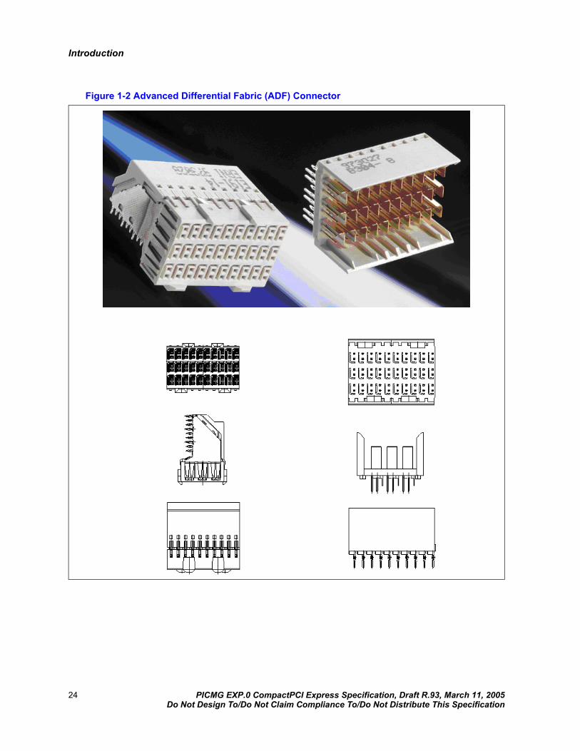
1.8.2 High-Speed Advanced Differential Fabric ConnectorsThis specification defines high-speed Advanced Differential Fabric (ADF) connectors to be used on System Slots/Boards, Type 1 Peripheral Slots/Boards, Type 2 Peripheral Slots/Boards, and Switch Slots/Boards. This ADF Connector is used mainly to carry the PCI Express signals and can support Generation 1 PCI Express signaling and potentially future generations of signaling.
Figure 1-2 shows the ADF connector.
PICMG EXP.0 CompactPCI Express Specification, Draft R.93, March 11, 2005 23Do Not Design To/Do Not Claim Compliance To/Do Not Distribute This Specification
Introduction
Figure 1-2 Advanced Differential Fabric (ADF) Connector
24 PICMG EXP.0 CompactPCI Express Specification, Draft R.93, March 11, 2005Do Not Design To/Do Not Claim Compliance To/Do Not Distribute This Specification

Introduction
1.8.3 UPM Power ConnectorsThe power connectors this specification defines are referred to as UPM Power Connectors.
1.8.3.1 System Slot/Board and Type 1 Peripheral Slot/Board
This specification defines a 7-position UPM Power Connector to be used on System Slots/Boards and Type 1 Peripheral Slots/Boards. The current handling of this connector provides enough power for high-performance CPUs.
Figure 1-3 shows the 7-position power connector.
Figure 1-3 UPM Power Connector for System and Type 1 Peripheral Slots/Boards
PICMG EXP.0 CompactPCI Express Specification, Draft R.93, March 11, 2005 25Do Not Design To/Do Not Claim Compliance To/Do Not Distribute This Specification
Introduction
1.8.3.2 Switch Slot/Board
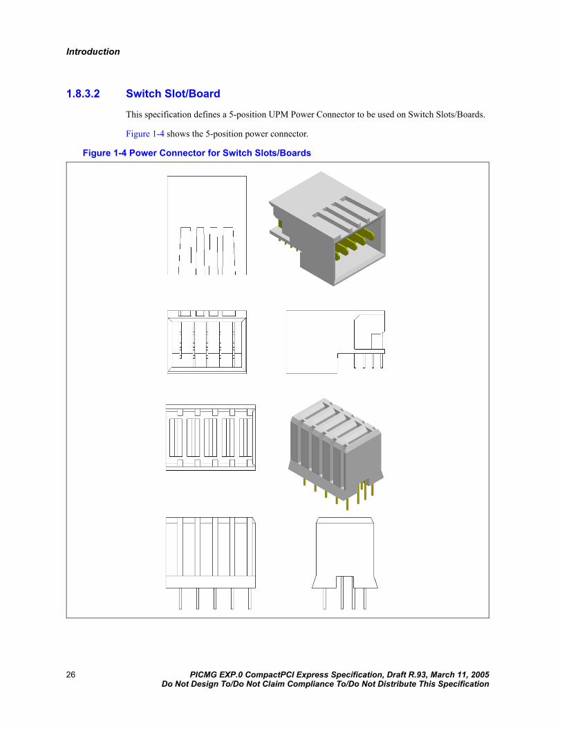
This specification defines a 5-position UPM Power Connector to be used on Switch Slots/Boards.
Figure 1-4 shows the 5-position power connector.
Figure 1-4 Power Connector for Switch Slots/Boards
26 PICMG EXP.0 CompactPCI Express Specification, Draft R.93, March 11, 2005Do Not Design To/Do Not Claim Compliance To/Do Not Distribute This Specification
Introduction
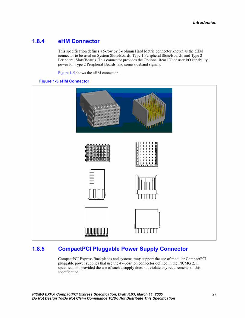
1.8.4 eHM ConnectorThis specification defines a 5-row by 8-column Hard Metric connector known as the eHM connector to be used on System Slots/Boards, Type 1 Peripheral Slots/Boards, and Type 2 Peripheral Slots/Boards. This connector provides the Optional Rear I/O or user I/O capability, power for Type 2 Peripheral Boards, and some sideband signals.
Figure 1-5 shows the eHM connector.
Figure 1-5 eHM Connector
1.8.5 CompactPCI Pluggable Power Supply ConnectorCompactPCI Express Backplanes and systems may support the use of modular CompactPCI pluggable power supplies that use the 47-position connector defined in the PICMG 2.11 specification, provided the use of such a supply does not violate any requirements of this specification.
PICMG EXP.0 CompactPCI Express Specification, Draft R.93, March 11, 2005 27Do Not Design To/Do Not Claim Compliance To/Do Not Distribute This Specification

Introduction
Figure 1-6 shows the 47-position CompactPCI pluggable power supply connector.
Figure 1-6 47-Position CompactPCI Pluggable Power Supply Connector
1.9 Slot and Board DescriptionsThis specification defines different slot and board types to meet the needs of different market segments, as well as ease the transition and speed the adoption of this standard. The slot types defined include a System Slot, a Type 1 Peripheral Slot, a Type 2 Peripheral Slot, a Hybrid Peripheral Slot, and a Switch Slot. The board types include a System Board, a Type 1 Peripheral Board, a Type 2 Peripheral Board, and a Switch Board. A Legacy Slot or Legacy Board refers to slots or Peripheral Boards defined in the PICMG 2.0 (CompactPCI) specification. These different board and slot types in the 6U form factor may include any or all of the J3/P3, J4/P4, and J5/P5 connectors defined in the PICMG 2.0 (CompactPCI) specification. The board examples in this section are shown as 3U boards for simplicity. The exception is the Switch Board, which is shown in both 3U and 6U for clarity.
Figure 1-7 shows the different 3U slot types.
28 PICMG EXP.0 CompactPCI Express Specification, Draft R.93, March 11, 2005Do Not Design To/Do Not Claim Compliance To/Do Not Distribute This Specification

Introduction
Figure 1-7 CompactPCI Express 3U Slot Examples
Figure 1-8 shows the different 6U slot types, along with the Optional P3, P4, and P5 connectors.
PICMG EXP.0 CompactPCI Express Specification, Draft R.93, March 11, 2005 29Do Not Design To/Do Not Claim Compliance To/Do Not Distribute This Specification

Introduction
Figure 1-8 CompactPCI Express 6U Slot Examples
OptionalConnectors
30 PICMG EXP.0 CompactPCI Express Specification, Draft R.93, March 11, 2005Do Not Design To/Do Not Claim Compliance To/Do Not Distribute This Specification

Introduction
1.9.1 Connector Reference DesignatorsSystem, Type 1, and Type 2 Slots/Boards share the same reference designator assignments with respect to connector type and position. The reference designator assignments start from the bottom at XJ1 for female connectors and at XP1 for male connectors. Note that the letter X has been added to the reference designator to indicate that it is a connector defined in this specification, and not leveraged from the PICMG 2.0 Specification (CompactPCI). Because a Type 2 Slot/Board does not have the bottom two connectors of a Type 1 or System Slot/Board, the Type 2 Slot/Board begins with XJ3 for female connectors and XP3 for male connectors.
Legacy Slots, Hybrid Peripheral Slots, and 6U Slots/Boards use HM connector reference designators leveraged from the PICMG 2.0 Specification (CompactPCI). The remaining connectors of these slot types have the same reference designator assignments with respect to connector type and position as a Type 1, Type 2, or System Slot/Board.
Switch Slots have their own unique numbering and start from the bottom at XSJ1 for female connectors and at XSP1 for male connectors.
1.9.2 System Slot and BoardA System Board provides two or four PCI Express Links that lead to the PCI Express Root Complex, along with their associated PCI Express reference clocks. It also provides the power supply control signaling, reset, and optionally SMBus master functionality. A System Board can be designed to work as a Type 1 Peripheral Board also. The System Board connectors include the XP1 7-position power connector, the XJ2 ADF connector, the XJ3 ADF connector, and the XJ4 eHM connector.
Figure 1-9 shows a System Board.
Figure 1-9 System Board
The System Slot is unique in a CompactPCI Express Chassis. It provides pins for the two or four PCI Express Links for routing from a System Board to PCI Express Switches, a Switch Slot for Link fan-out, or directly to Peripheral Slots. The System Slot connectors include the XJ1 7-position power connector, the XP2 ADF connector, the XP3 ADF connector, and the XP4 eHM connector.
Figure 1-10 shows a System Slot.
XJ4
XJ3
XJ2
XP1
PICMG EXP.0 CompactPCI Express Specification, Draft R.93, March 11, 2005 31Do Not Design To/Do Not Claim Compliance To/Do Not Distribute This Specification

Introduction
Figure 1-10 System Slot
The 6U form factor of the System Board/Slot may include any or all of the J3/P3, J4/P4, and J5/P5 connectors defined in the PICMG 2.0 (CompactPCI) specification.
1.9.3 Type 1 Peripheral Slot and Board A Type 1 Peripheral Board has access to two PCI Express Links. The Type 1 Peripheral Board connectors include the XP1 7-position power connector, the XJ2 ADF connector, the XJ3 ADF connector, and the XJ4 eHM connector.
Figure 1-11 shows a Type 1 Peripheral Board.
Figure 1-11 Type 1 Peripheral Board
XP4
XP3
XP2
XJ1
XJ4
XJ3
XJ2
XP1
32 PICMG EXP.0 CompactPCI Express Specification, Draft R.93, March 11, 2005Do Not Design To/Do Not Claim Compliance To/Do Not Distribute This Specification

Introduction
There may be multiple Type 1 Peripheral Slots in a CompactPCI Express Chassis. The PCI Express Links connected to the Type 1 Peripheral Slots shall be connected to either a PCI Express Switch, Switch Slot, or directly to the System Slot. Type 1 Peripheral Slots support both Type 1 and Type 2 Peripheral Boards. The Type 1 Peripheral Slot connectors include the XJ1 7-position power connector, the XP2 ADF connector, the XP3 ADF connector, and the XP4 eHM connector.
Figure 1-12 shows a Type 1 Peripheral Slot.
Figure 1-12 Type 1 Peripheral Slot
The 6U form factor of the Type 1 Peripheral Board/Slot may include any or all of the J3/P3, J4/P4, and J5/P5 connectors defined in the PICMG 2.0 (CompactPCI) specification.
1.9.4 Type 2 Peripheral Slot and Board A Type 2 Peripheral Board has access to one PCI Express Link. The Type 2 Peripheral Board connectors include the XJ3 ADF connector and XJ4 eHM connector.
Figure 1-13 shows a Type 2 Peripheral Board.
XP4
XP3
XP2
XJ1
PICMG EXP.0 CompactPCI Express Specification, Draft R.93, March 11, 2005 33Do Not Design To/Do Not Claim Compliance To/Do Not Distribute This Specification

Introduction
Figure 1-13 Type 2 Peripheral Board
There may be multiple Type 2 Peripheral Slots in a CompactPCI Express Chassis. The PCI Express Links connected to the Type 2 Peripheral Slots may be connected to a PCI Express Switch, Switch Slot, or directly to the System Slot. The Type 2 Peripheral Slot connectors include the XP3 ADF connector and the XP4 eHM connector.
Figure 1-14 shows a Type 2 Peripheral Slot.
Figure 1-14 Type 2 Peripheral Slot
The 6U form factor of the Type 2 Board/Slot may include any or all of the J3/P3, J4/P4, and J5/P5 connectors defined in the PICMG 2.0 (CompactPCI) specification.
XJ3
XJ4
XP4
XP3
34 PICMG EXP.0 CompactPCI Express Specification, Draft R.93, March 11, 2005Do Not Design To/Do Not Claim Compliance To/Do Not Distribute This Specification

Introduction
1.9.5 Hybrid Peripheral SlotA Hybrid Peripheral Slot supports either a Type 2 Peripheral Board, a 32-bit CompactPCI Board, or a PXI Board with an eHM connector populated instead of the J2 connector. This allows a single slot to work with new or existing products. The Hybrid Peripheral Slot connectors include the P1 connector defined in the PICMG 2.0 (Compact PCI) specification, the XP3 ADF connector, and the XP4 eHM connector.
Figure 1-15 shows a Hybrid Peripheral Slot, and Figure 1-16 shows the different boards that can be used in Hybrid Peripheral Slots.
Figure 1-15 Hybrid Peripheral Slot
XP4
XP3
P1
PICMG EXP.0 CompactPCI Express Specification, Draft R.93, March 11, 2005 35Do Not Design To/Do Not Claim Compliance To/Do Not Distribute This Specification

Introduction
Figure 1-16 Boards Supported By Hybrid Peripheral Slots
There may be multiple Hybrid Peripheral Slots in a CompactPCI Express Chassis.
The 6U form factor of the Hybrid Board/Slot may include any or all of the J3/P3, J4/P4, and J5/P5 connectors defined in the PICMG 2.0 (CompactPCI) specification.
1.9.6 Legacy SlotA Legacy Slot is a Peripheral Slot as defined by the PICMG 2.0 (CompactPCI) specification. Refer to the PICMG 2.0 specification for details. There may be multiple Legacy Slots in a CompactPCI Express Chassis.
1.9.7 Switch Slot and BoardThis specification defines a Switch Slot/Board in a 3U and 6U form factor that is Optional for CompactPCI Express systems. A Switch Board provides a standard modular way for a CompactPCI Express system to provide PCI Express Link fan-out from the System Slot to multiple Peripheral Slots. The 3U Switch Slot/Board pin assignments are a subset of the 6U Switch Slot/Board. The 3U Switch Slot/Board power connector and ADF connector spacing are mechanically identical to the 6U Switch Slot/Board. There may be multiple Switch Slots in a CompactPCI Express Chassis.
1.9.7.1 3U Switch Slot and Board
The 3U Switch Board definition includes the XSP1 5-position power connector, XSJ2 ADF connector, XSJ3 ADF connector, and XSJ4 ADF connector.
Figure 1-17 shows a 3U Switch Board.
Type 2 Board 32-Bit CompactPCI Board PXI Board
36 PICMG EXP.0 CompactPCI Express Specification, Draft R.93, March 11, 2005Do Not Design To/Do Not Claim Compliance To/Do Not Distribute This Specification

Introduction
Figure 1-17 3U Switch Board
The 3U Switch Slot includes the XSJ1 5-position power connector, XSP2 ADF connector, XSP3 ADF connector, and XSP4 ADF connector.
Figure 1-18 shows a 3U Switch Slot.
Figure 1-18 3U Switch Slot
1.9.7.2 6U Switch Slot and Board
The 6U Switch Board includes the XSP1 5-position power connector and XSJ2, XSJ3, XSJ4, XSJ5, XSJ6, XSJ7, XSJ8, and XSJ9 ADF connectors.
Figure 1-19 shows a 6U Switch Board.
XSJ4
XSJ3
XSJ2
XSP1
XSP4
XSP3
XSP2
XSJ1
PICMG EXP.0 CompactPCI Express Specification, Draft R.93, March 11, 2005 37Do Not Design To/Do Not Claim Compliance To/Do Not Distribute This Specification
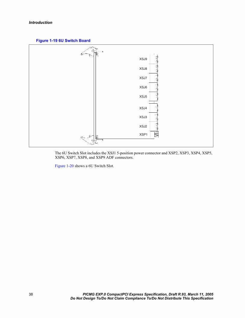
Introduction
Figure 1-19 6U Switch Board
The 6U Switch Slot includes the XSJ1 5-position power connector and XSP2, XSP3, XSP4, XSP5, XSP6, XSP7, XSP8, and XSP9 ADF connectors.
Figure 1-20 shows a 6U Switch Slot.
XSJ9
XSJ8
XSJ7
XSJ6
XSJ5
XSJ4
XSJ3
XSJ2
XSP1
38 PICMG EXP.0 CompactPCI Express Specification, Draft R.93, March 11, 2005Do Not Design To/Do Not Claim Compliance To/Do Not Distribute This Specification

Introduction
Figure 1-20 6U Switch Slot
XSP9
XSP8
XSP7
XSP6
XSP5
XSP4
XSP3
XSP2
XSJ1
PICMG EXP.0 CompactPCI Express Specification, Draft R.93, March 11, 2005 39Do Not Design To/Do Not Claim Compliance To/Do Not Distribute This Specification

Introduction
1.10 Example ConfigurationsThis specification enables numerous connector type and Backplane routing possibilities.
Figure 1-21 through Figure 1-25 show a few slot type and routing possibilities.
Figure 1-21 Backplane with Hybrid Peripheral Slots and Legacy Slots
System Slot
HybridPeripheral Slots
Legacy Peripheral Slots
x4 PCIe
x4 PCIe
x4 PCIe
x4 PCIe
PCI Bus
PCIe toPCI Bridge
40 PICMG EXP.0 CompactPCI Express Specification, Draft R.93, March 11, 2005Do Not Design To/Do Not Claim Compliance To/Do Not Distribute This Specification

Introduction
Figure 1-22 Backplane with all Hybrid Peripheral Slots
System Slot
HybridPeripheral Slots
x8 PCIe
x8 PCIe
x4 PCIex4 PCIe
x4 PCIe
x4 PCIex4 PCIe
x4 PCIe
x4 PCIe
PCI Bus Segment 1 PCI Bus Segment 2
x4 PCIe
16-lane Switch
32-lane Switch
PCIe Switch
PCIe Switch
PCIe toPCI Bridge
PICMG EXP.0 CompactPCI Express Specification, Draft R.93, March 11, 2005 41Do Not Design To/Do Not Claim Compliance To/Do Not Distribute This Specification

Introduction
Figure 1-23 Backplane with Type 2 and Hybrid Peripheral Slots
System Slot
HybridPeripheral Slots
x8 PCIe
x8 PCIe
x4 PCIex4 PCIe
x4 PCIe
x4 PCIe
x1 PCIe
x4 PCIe
PCI Bus
x4 PCIe
16-lane Switch
32-lane Switch
x4 PCIe
16-lane Switch
...
...Type 2Peripheral Slots
PCIe toPCI Bridge
PCIe Switch
PCIe Switch
PCIe Switch
42 PICMG EXP.0 CompactPCI Express Specification, Draft R.93, March 11, 2005Do Not Design To/Do Not Claim Compliance To/Do Not Distribute This Specification
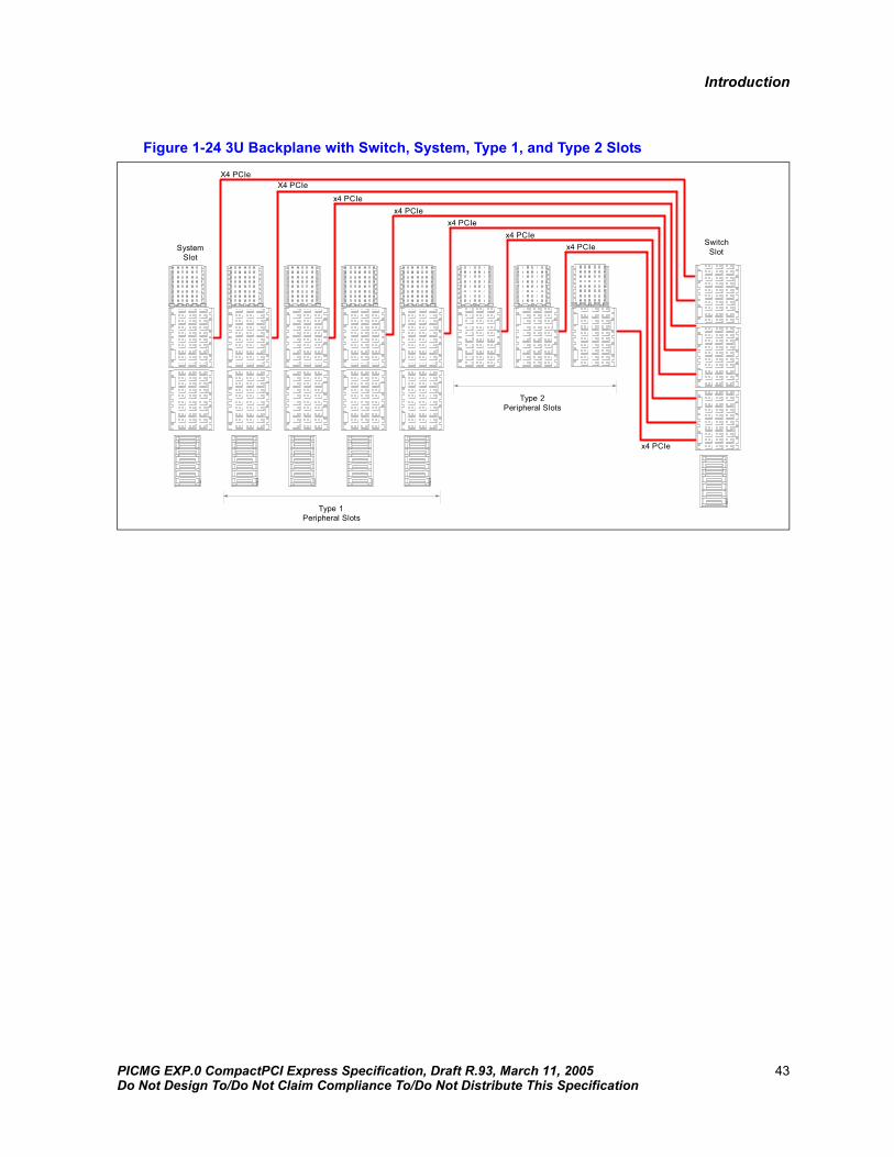
Introduction
Figure 1-24 3U Backplane with Switch, System, Type 1, and Type 2 Slots
System Slot
SwitchSlot
X4 PCIe
x4 PCIex4 PCIe
x4 PCIe
x4 PCIe
Type 2Peripheral Slots
x4 PCIe
Type 1Peripheral Slots
x4 PCIe
X4 PCIe
PICMG EXP.0 CompactPCI Express Specification, Draft R.93, March 11, 2005 43Do Not Design To/Do Not Claim Compliance To/Do Not Distribute This Specification
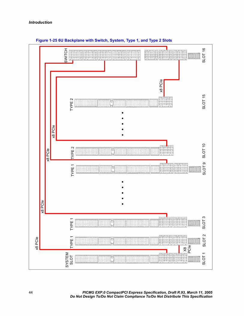
Introduction
Figure 1-25 6U Backplane with Switch, System, Type 1, and Type 2 Slots
SLO
T 1
X8 PCIe
x8 P
CIe
x8 P
CIe
x8 P
CIe
x8 P
CIe
x8 P
CIe
SW
ITC
HTY
PE
2TY
PE
2TY
PE 1
TYP
E 1
TYP
E 1
SLO
T 2
SLO
T 3
SLO
T 9
SLO
T 10
SLO
T 15
SLO
T 16
SYS
TEM
SLO
T
44 PICMG EXP.0 CompactPCI Express Specification, Draft R.93, March 11, 2005Do Not Design To/Do Not Claim Compliance To/Do Not Distribute This Specification

Mechanical Requirements
Mechanical Requirements 2
2.1 Mechanical OverviewThis section defines the mechanical requirements for CompactPCI Express platforms. Specifically, it provides details for the connectors, Backplanes, and boards the specification defines. In general, CompactPCI Express Backplanes and plug-in board dimensions are in accordance with PICMG-2.0, IEEE 1101.1, and 1101.10. In the event of discrepancies, this specification shall override. It is assumed that board, Backplane, and Chassis designers are familiar with these specifications.
2.2 Drawing StandardThe drawings in this specification shall be interpreted per ASME Y14.100.
2.3 UnitsThe units in the drawings in this standard are in millimeters unless otherwise noted.
2.4 Keepout ZonesUnless explicitly stated otherwise, all keepout zones defined in this specification shall apply to both sides of the PCB.
2.5 Connector RequirementsCompactPCI Express uses the connectors as outlined in Section 1.6 and appendices A, B, and C.
2.5.1 ADF ConnectorsAppendix A contains the requirements for the ADF Connectors.
2.5.1.1 Board Connectors
CompactPCI Express Boards shall use the ADF Connector with type designation of ADF-F-3-10-2-F-25.
PICMG EXP.0 CompactPCI Express Specification, Draft R.93, March 11, 2005 45Do Not Design To/Do Not Claim Compliance To/Do Not Distribute This Specification

Mechanical Requirements
2.5.1.2 Backplane Connectors without Hot-Plug Support
CompactPCI Express Backplane slots that do not support Hot-Plug shall use the ADF Connector with type designation ADF-M-3-10-2-B-25 or ADF-M-3-10-2-S-B-25-0100.
2.5.1.3 Backplane Connectors with Hot-Plug Support
CompactPCI Express Backplane slots that support Hot-Plug shall use the use the ADF Connector with type designation ADF-M-3-10-2-S-B-25-0100 for the XP3 connector and shall use the ADF Connector with type designation ADF-M-3-10-2-B-25 or ADF-M-3-10-2-S-B-25-0100 for any remaining ADF connectors.
2.5.2 eHM ConnectorsAppendix B contains the requirements for the eHM Connectors.
2.5.2.1 Board Connector Type Designation
CompactPCI Express Boards shall use the eHM Connector with type designation of eHM-FN, where N is the appropriate keying designator depending on eHM I/O pin use defined in Section 4.2.
2.5.2.2 Backplane Connectors without Hot-Plug Support
CompactPCI Express Backplane slots that do not support Hot-Plug and use pins for Rear I/O shall use the eHM Connector with type designation eHM-MN-HP-RX or eHM-MN-RX, where N is the appropriate keying designator depending on eHM I/O pin use defined in Section 4.2.
CompactPCI Express Backplane slots that do not support Hot-Plug and do not use pins for Rear I/O shall use the eHM Connector with type designation eHM-MN-HP or eHM-MN, where N is the appropriate keying designator depending on eHM I/O pin use defined in Section 4.2.
2.5.2.3 Backplane Connectors with Hot-Plug Support
CompactPCI Express Backplane slots that support Hot-Plug and use pins for Rear I/O shall use the eHM Connector with type designation eHM-MN-HP-RX, where N is the appropriate keying designator depending on eHM I/O pin use defined in Section 4.2.
CompactPCI Express Backplane slots that support Hot-Plug and do not use pins for Rear I/O shall use the eHM Connector with type designation eHM-MN-HP, where N is the appropriate keying designator depending on eHM I/O pin use defined in Section 4.2.
2.5.3 UPM ConnectorsAppendix C contains the requirements for the UPM Connectors.
2.5.3.1 Backplane Connectors
System Boards and Type 1 Boards shall use the UPM connector with type designation UPM-F-7.
46 PICMG EXP.0 CompactPCI Express Specification, Draft R.93, March 11, 2005Do Not Design To/Do Not Claim Compliance To/Do Not Distribute This Specification

Mechanical Requirements
Switch Boards shall use the UPM connector with type designation UPM-F-5.
2.5.3.2 Board Connectors without Hot-Plug Support
Type 1 Slots that do not support Hot-Plug shall use the UPM connector with type designation UPM-M-7 or UPM-M-7-HP.
System Slots shall use the UPM connector with type designation UPM-M-7 or UPM-M-7-HP.
Switch Slots shall use the UPM connector with type designation UPM-M-5.
2.5.3.3 Board Connectors with Hot-Plug Support
Type 1 Slots that support Hot-Plug shall use the UPM connector with type designation UPM-M-7-HP.
2.5.4 HM ConnectorsSee IEC 61076-4-101.
2.5.5 47-Position Pluggable Power Supply ConnectorSee PICMG 2.11.
2.6 Chassis Subrack RequirementsCompactPCI Express Chassis shall use PICMG 2.0-compliant Chassis Subracks.
2.7 Backplane RequirementsCompactPCI Express defines the 3U/6U Backplanes as shown in this section.
2.7.1 3U Backplane Dimensions and Connector LocationsFigure 2-1 and Figure 2-2 define the dimensional requirements that 3U CompactPCI Express Backplanes shall meet. Note that all slot types are shown for clarity. Each application may define how many of which slot types are used and what order they are in.
PICMG EXP.0 CompactPCI Express Specification, Draft R.93, March 11, 2005 47Do Not Design To/Do Not Claim Compliance To/Do Not Distribute This Specification

Mechanical Requirements
Figure 2-1 Backplane Overall Dimensions
48 PICMG EXP.0 CompactPCI Express Specification, Draft R.93, March 11, 2005Do Not Design To/Do Not Claim Compliance To/Do Not Distribute This Specification

Mechanical Requirements
Figure 2-2 3U Backplane Connector Locations
2.7.2 6U Backplane Dimensions and Connector LocationsFigure 2-3 defines the dimensional requirements that 6U CompactPCI Express Backplanes shall meet. Note that all slot types are shown for clarity. Each application may define how many of which slot types are used and what order they are in.
PICMG EXP.0 CompactPCI Express Specification, Draft R.93, March 11, 2005 49Do Not Design To/Do Not Claim Compliance To/Do Not Distribute This Specification

Mechanical Requirements
Figure 2-3 6U Backplane Connector Locations
50 PICMG EXP.0 CompactPCI Express Specification, Draft R.93, March 11, 2005Do Not Design To/Do Not Claim Compliance To/Do Not Distribute This Specification

Mechanical Requirements
2.8 Slot Numbering and GlyphsFigure 2-4 shows the board compatibility glyphs that shall be displayed on the front panel by board type.
Figure 2-4 Board Compatibility Glyphs
Boards that can be used in either a System Slot or Peripheral Slot shall combine both compatibility glyphs as shown in Figure 2-5.
Figure 2-5 Glyph for Boards that Operate in Either System or Peripheral Slots
Physical Slot locations within the Subrack shall be indicated by a numbering scheme visible from the front of the Subrack. These Physical Slot numbers shall be placed within the compatibility glyphs as shown in Figure 2-6.
Figure 2-6 Slot Compatibility Glyphs
2.9 Board RequirementsCompactPCI Express defines the 3U/6U board sizes as described in this section.
2.9.1 3U System/Type 1/Type 2 Board Dimensions and Connector LocationsFigure 2-7 defines the board dimensions and connector locations that 3U System, Type 1, and Type 2 Boards shall meet. Note that a Type 2 Board does not use the XP1 and XJ2 connectors.
Peripheral BoardSystem Board Switch Board
System or Peripheral Board
2 3
Peripheral Slot
1System Slot Switch Slot
PICMG EXP.0 CompactPCI Express Specification, Draft R.93, March 11, 2005 51Do Not Design To/Do Not Claim Compliance To/Do Not Distribute This Specification

Mechanical Requirements
Figure 2-7 3U System, Type 1, and Type 2 Board Dimensions and Connector Locations
52 PICMG EXP.0 CompactPCI Express Specification, Draft R.93, March 11, 2005Do Not Design To/Do Not Claim Compliance To/Do Not Distribute This Specification

Mechanical Requirements
2.9.2 6U System/Type 1/Type 2 Board Dimensions and Connector LocationsFigure 2-8 defines the board dimensions and connector locations that 6U System, Type 1, and Type 2 Boards shall meet. Note that a Type 2 Board does not use the XP1 and XJ2 connectors.
Figure 2-8 6U System/Type 1/Type 2 Board Dimensions and Connector Locations
PICMG EXP.0 CompactPCI Express Specification, Draft R.93, March 11, 2005 53Do Not Design To/Do Not Claim Compliance To/Do Not Distribute This Specification

Mechanical Requirements
2.9.3 3U Switch Board Dimensions and Connector LocationsFigure 2-9 defines the board dimensions and connector locations that a 3U Switch Board shall meet.
Figure 2-9 3U Switch Board Dimensions and Connector Locations
54 PICMG EXP.0 CompactPCI Express Specification, Draft R.93, March 11, 2005Do Not Design To/Do Not Claim Compliance To/Do Not Distribute This Specification
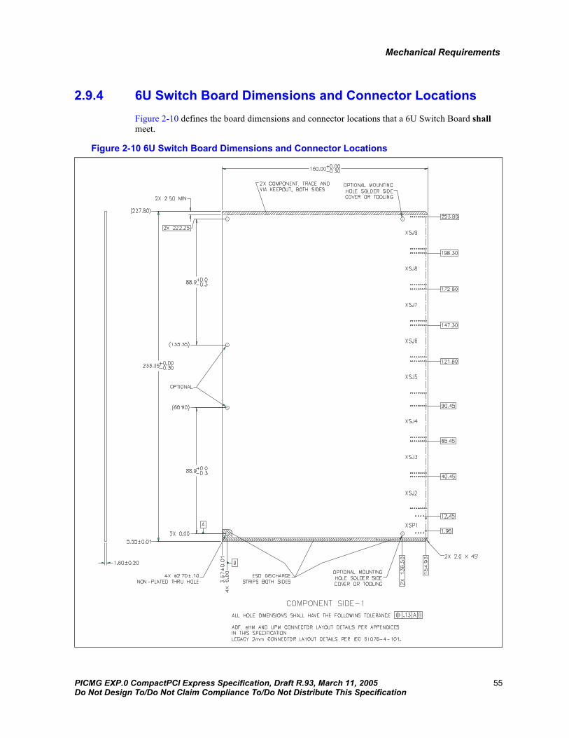
Mechanical Requirements
2.9.4 6U Switch Board Dimensions and Connector LocationsFigure 2-10 defines the board dimensions and connector locations that a 6U Switch Board shall meet.
Figure 2-10 6U Switch Board Dimensions and Connector Locations
PICMG EXP.0 CompactPCI Express Specification, Draft R.93, March 11, 2005 55Do Not Design To/Do Not Claim Compliance To/Do Not Distribute This Specification

Mechanical Requirements
2.9.5 Board PCB ThicknessCompactPCI Express Board PCB’s shall be 1.6 mm ± 0.2 mm within the Card Guide keepout area, as defined in Figure 2-7. PCB’s requiring a greater thickness shall have material removed from Component side-2 to meet the above requirements. See Figure 2-11 for more details.
Figure 2-11 Modification to PCB to Support Thicker Boards
2.9.6 ESD Discharge StripPICMG 2.0 requirements for ESD discharge strips shall be followed for CompactPCI Express.
2.9.7 ESD ClipPICMG 2.0 requirements for ESD clips shall be followed for CompactPCI Express.
2.9.8 Front PanelsPICMG 2.0 requirements for front panels shall be followed for CompactPCI Express, with the exception that Section 2.8 of this specification defines glyphs, and Section 2.9.9 defines the CompactPCI Express logo.
FrontPanel
PCB
GuideRail
4 HP Typ.(20.32)
Interboard Separation Plane
Component
PCB Milled inCarguide Areafrom Solder Side
PCB Thicker than Carguide Can Accept1.6 mm PCB
Detail Showing How a PCB Thickerthan the Cardguide Slot Will Accept,Could Be Modified in the Guide RailArea to Allow to Fit
56 PICMG EXP.0 CompactPCI Express Specification, Draft R.93, March 11, 2005Do Not Design To/Do Not Claim Compliance To/Do Not Distribute This Specification
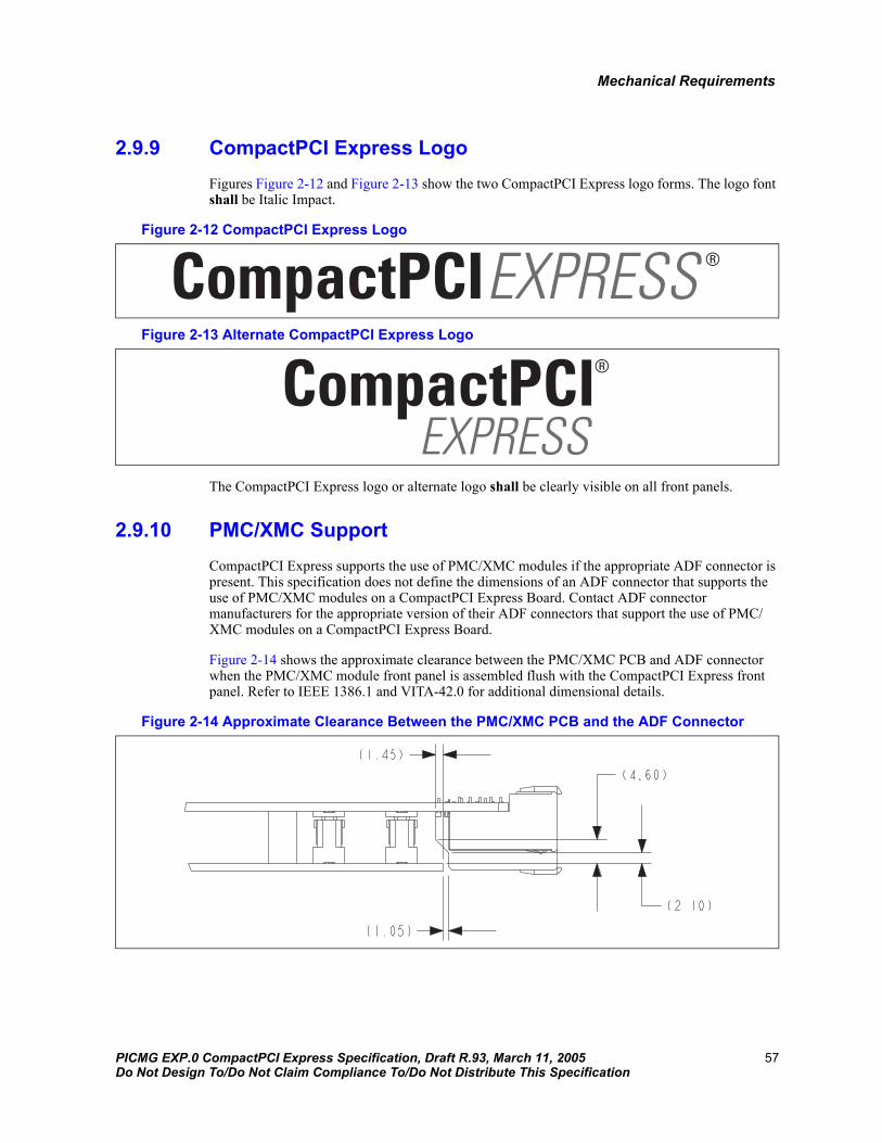
Mechanical Requirements
2.9.9 CompactPCI Express LogoFigures Figure 2-12 and Figure 2-13 show the two CompactPCI Express logo forms. The logo font shall be Italic Impact.
Figure 2-12 CompactPCI Express Logo
Figure 2-13 Alternate CompactPCI Express Logo
The CompactPCI Express logo or alternate logo shall be clearly visible on all front panels.
2.9.10 PMC/XMC SupportCompactPCI Express supports the use of PMC/XMC modules if the appropriate ADF connector is present. This specification does not define the dimensions of an ADF connector that supports the use of PMC/XMC modules on a CompactPCI Express Board. Contact ADF connector manufacturers for the appropriate version of their ADF connectors that support the use of PMC/XMC modules on a CompactPCI Express Board.
Figure 2-14 shows the approximate clearance between the PMC/XMC PCB and ADF connector when the PMC/XMC module front panel is assembled flush with the CompactPCI Express front panel. Refer to IEEE 1386.1 and VITA-42.0 for additional dimensional details.
Figure 2-14 Approximate Clearance Between the PMC/XMC PCB and the ADF Connector
PICMG EXP.0 CompactPCI Express Specification, Draft R.93, March 11, 2005 57Do Not Design To/Do Not Claim Compliance To/Do Not Distribute This Specification

Mechanical Requirements
2.9.11 Cross Sectional ViewFigure 2-15 provides a board cross-sectional view of several key features including connectors, front panel, ejector/injector, Component sides, etc.
Figure 2-15 Board Cross-Sectional View
2.9.12 Component Outline and WarpagePICMG 2.0 requirements shall be followed for CompactPCI Express.
2.9.13 Solder Side Cover (Optional)PICMG 2.0 requirements shall be followed for CompactPCI Express.
58 PICMG EXP.0 CompactPCI Express Specification, Draft R.93, March 11, 2005Do Not Design To/Do Not Claim Compliance To/Do Not Distribute This Specification

Mechanical Requirements
2.9.14 Component HeightsPICMG 2.0 requirements for Components heights shall be followed for CompactPCI Express. It is suggested that Component side-2 heights, as called out in Figure 2-15, should be used to minimize the possibility of Component damage during board insertion/extraction when a Component side-2 cover is not used.
2.9.15 System Slot IdentificationSystem Slot location shall be indicated within a CompactPCI Express Subrack by red Guide Rails. This allows users to locate the System Slot easily. Peripheral Slots and Switch Slots shall not use red Guide Rails.
2.10 Rear-Panel I/O Board Requirements6U CompactPCI Express Boards may populate any or all of the J3, J4, and J5 connectors. J3, J4, and J5 may be used for rear-panel I/O. Rear-panel I/O may be defined by the user and/or use PICMG specifications. Contact PICMG for copies of these specifications.
3U CompactPCI Express Boards may use pins of the XJ4 connector labeled I/O in the pin assignment tables in Chapter 3 for rear-panel I/O.
The same front panel, handles, keying, alignment pin, EMC, and ESD mechanics should be used as on the front CompactPCI Express Boards. The same Subrack rails, Guide Rails, EMC support, ESD support, keying, alignment pin hole, and injector/extractor comb should be used as on the Subrack front side, except for the Card Guide’s depth. Note that rear-panel I/O transition boards are “in-line” with the front CompactPCI Express Boards. This means the front panels of rear-panel I/O transition boards are reversed (mirrored) from the front boards. The top handles are on the bottom, and the bottom handles are on the top. The slot keying holes and hole labels in both the Card Guides and front panels are upside down as compared to the front boards and Card Guides.
The same connector pin labeling sequence should be used on the Rear I/O transition boards as the on front boards. Effectively, this is a mirror image of the front board’s layout orientation. Using the same 1-for-1 pin mapping labeling sequence eliminates confusion and I/O signal pin mapping problems. For example, pin J5:A3 of the front board connects to P5:A3 of the Backplane. The signal is available as RP5:A3 from the rear of the Backplane and connects to RJ5:A3 of the Rear I/O module.
2.10.1 3U Rear-Panel I/O Board Dimensions3U rear-panel I/O boards shall be 80 mm in depth. Figure 2-16 defines a 3U 80 mm representative rear-panel I/O board as IEEE 1101.11 defines. Refer to IEEE 1101.11 for further details.
Section 4.2 gives the requirements for keying CompactPCI Express Boards with rear-panel I/O on the eHM connector. The keying combination on the rear panel I/O module shall match that on the corresponding CompactPCI Express Board.
PICMG EXP.0 CompactPCI Express Specification, Draft R.93, March 11, 2005 59Do Not Design To/Do Not Claim Compliance To/Do Not Distribute This Specification

Mechanical Requirements
Figure 2-16 3U Rear-Panel I/O Board Dimensions
2.10.2 6U Rear-Panel I/O Board Dimensions6U rear-panel I/O boards shall be 80 mm in depth. Figure 2-17 defines a 6U 80 mm representative rear-panel I/O board as IEEE 1101.11 defines. Refer to IEEE 1101.11 for further details.
6U rear-panel I/O shall be keyed to conform to the PICMG 2.10, Keying of CompactPCI Boards and Backplanes specification. The keying combination on the rear panel I/O module shall match that on the corresponding CompactPCI Express Board. Note that RP3/RJ3 and RP5/RJ5 positions are implemented with type AB connectors.
60 PICMG EXP.0 CompactPCI Express Specification, Draft R.93, March 11, 2005Do Not Design To/Do Not Claim Compliance To/Do Not Distribute This Specification

Mechanical Requirements
Figure 2-17 6U Rear-Panel I/O Board Dimensions
PICMG EXP.0 CompactPCI Express Specification, Draft R.93, March 11, 2005 61Do Not Design To/Do Not Claim Compliance To/Do Not Distribute This Specification

Electrical Requirements
Electrical Requirements 3
3.1 Signal DefinitionsThis section details the signals this specification uses. This specification leverages standards that define many of the signals. Where appropriate, the standard this specification leverages is referenced.
3.1.1 PCI Express SignalsThe electrical requirements in this specification are based on first-generation PCI Express signaling at 2.5 Gb/s data rates. A future revision of this specification may support future generations of PCI Express supporting faster data rates.
3.1.1.1 PCI Express Transmit Signals
The PCI Express transmit signals yPETpx and yPETnx are named with the following convention: “y” is the Link within a slot or on a board, “PE” stands for PCI Express, “T” stands for Transmitter, “p” is the positive signal, “n” is the negative signal, and “x” is the Lane within a slot or on a board.
The signal characteristic requirements for the PCI Express transmit signals are defined in the PCI-SIG PCI Express Base Specification in the Differential Transmitter (TX) Output section.
The rules and permissions regarding polarity inversion and Lane reversal called out in the PCI-SIG PCI Express Base Specification apply.
The yPETpx and yPETnx pins on a System Board’s connectors shall be connected to the PCI Express Transmitter differential pairs on the Component providing the PCI Express Links. The PETpx and PETnx pins on Peripheral Board’s connectors shall be connected to the PCI Express Transmitter differential pairs on the Component accepting the PCI Express Links. This connection scheme is one of the requirements necessary to allow System Boards to be designed to work in Type 1 Peripheral Slots.
The PETpx and PETnx pins on Switch Board’s Upstream connector shall be connected to the PCIe Transmitter differential pairs on the Component accepting the PCIe Links. The yPETpx and yPETnx pins on a Switch Board’s Downstream connectors shall be connected to the PCIe Transmitter differential pairs on the Component providing the PCIe Links.
3.1.1.2 PCI Express Receive Signals
The PCI Express receive signals yPERpx and yPERnx are named with the following convention: “y” is the Link within a slot or on a board, “PE” stands for PCI Express, “R” stands for Receiver, “p” is the positive signal, “n” is the negative signal, and “x” is the Lane within a slot or on a board.
The signal characteristic requirements for the PCI Express receive signals are defined in the PCI-SIG PCI Express Base Specification in the Differential Receiver (RX) Input section.
The rules and permissions regarding polarity inversion and Lane reversal called out in the PCI-SIG PCI Express Base Specification apply.
62 PICMG EXP.0 CompactPCI Express Specification, Draft R.93, March 11, 2005Do Not Design To/Do Not Claim Compliance To/Do Not Distribute This Specification

Electrical Requirements
The yPERpx and yPERnx pins on a System Board’s connectors shall be connected to the PCI Express Receiver differential pairs on the Component providing the PCI Express Links. The PERpx and PERnx pins on Peripheral Board’s connectors shall be connected to the PCI Express Receiver differential pairs on the Component accepting the PCI Express Links. This connection scheme is one of the requirements necessary to allow System Boards to be designed to work in Type 1 Peripheral Slots.
The yPERpx and yPERnx pins on a Switch Board’s Upstream connector shall be connected to the PCIe Receiver differential pairs on the Component providing the PCIe Links. The PERpx and PERnx pins on Switch Board’s Downstream connectors shall be connected to the PCIe Receiver differential pairs on the Component accepting the PCIe Links.
3.1.1.3 Interconnect Definition
In the context of this specification, the interconnect is comprised of everything between the pins of a Transmitter package and the pins of a Receiver package. This consists of traces on printed circuit boards, vias, AC coupling capacitors, and connectors. The interconnect total capacitance to ground seen by the Receiver Detection circuit shall not exceed 3 nF, including capacitance added by any attached test instrumentation. Note that this capacitance is separate and distinct from the AC Coupling capacitance value.
3.1.1.3.1 Link Definition
Typical CompactPCI Express Links, from source to destination, consist of the following:
• ASIC Transmitters on a printed circuit board
• Package fan-in-out trace topologies
• AC-coupling capacitors
• PCB coupled microstrip and/or stripline traces
• Vias for Layer changes
• Mated Backplane connector
• Backplane stripline routes
• Mated Backplane connector
• Coupled microstrip and/or stripline traces
• Package fan-in-out trace topologies
• ASIC Receivers on a printed circuit board
3.1.1.3.2 Link Grouping
The electrical parameters for the Link are subdivided into three Components.
• Peripheral Board interconnect (no connector)
• Backplane including mated connectors
• System Board and Switch Board interconnect (no connector)
PICMG EXP.0 CompactPCI Express Specification, Draft R.93, March 11, 2005 63Do Not Design To/Do Not Claim Compliance To/Do Not Distribute This Specification
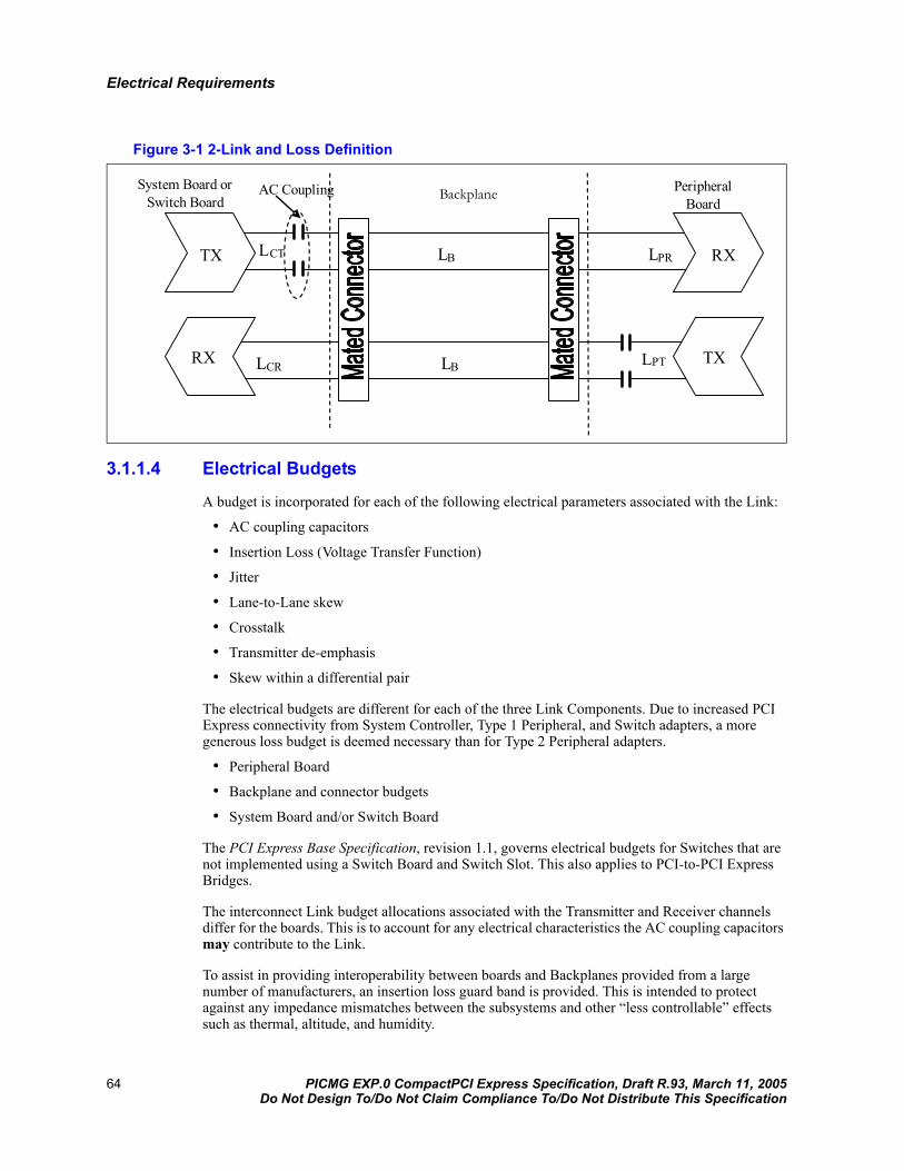
Electrical Requirements
Figure 3-1 2-Link and Loss Definition
3.1.1.4 Electrical Budgets
A budget is incorporated for each of the following electrical parameters associated with the Link:
• AC coupling capacitors
• Insertion Loss (Voltage Transfer Function)
• Jitter
• Lane-to-Lane skew
• Crosstalk
• Transmitter de-emphasis
• Skew within a differential pair
The electrical budgets are different for each of the three Link Components. Due to increased PCI Express connectivity from System Controller, Type 1 Peripheral, and Switch adapters, a more generous loss budget is deemed necessary than for Type 2 Peripheral adapters.
• Peripheral Board
• Backplane and connector budgets
• System Board and/or Switch Board
The PCI Express Base Specification, revision 1.1, governs electrical budgets for Switches that are not implemented using a Switch Board and Switch Slot. This also applies to PCI-to-PCI Express Bridges.
The interconnect Link budget allocations associated with the Transmitter and Receiver channels differ for the boards. This is to account for any electrical characteristics the AC coupling capacitors may contribute to the Link.
To assist in providing interoperability between boards and Backplanes provided from a large number of manufacturers, an insertion loss guard band is provided. This is intended to protect against any impedance mismatches between the subsystems and other “less controllable” effects such as thermal, altitude, and humidity.
AC Coupling
LCT
LCR LPT
LPRTX
TXRX
RX
System Board or Switch Board
Peripheral Board
Backplane
LB
LB
64 PICMG EXP.0 CompactPCI Express Specification, Draft R.93, March 11, 2005Do Not Design To/Do Not Claim Compliance To/Do Not Distribute This Specification

Electrical Requirements
By no means is this loss budget definition and allocation intended to limit any potential system architectures. It is the system/Backplane designer’s responsibility to test for compliance against this specification to guarantee interoperability with the large number of boards, compliant with this specification, which might become available.
3.1.1.4.1 AC Coupling
Each Lane of a Link shall be AC coupled. The requirement for the inclusion of AC coupling capacitors on the interconnect is specified at the Transmitter. A maximum 0603-type (or smaller 0402-type) capacitor package size is suggested, with a value as specified in the PCI Express Base Specification. The coupling capacitors of packages larger than 0603 may cause additional attenuation or jitter. This attenuation or jitter shall be accounted for as part of the budget allocation for the physical interconnect path of the board the capacitors are mounted on. The allocated budget includes the electrical parasitic effects associated with typical Component placement as mounted on the printed circuit board.
3.1.1.4.2 Insertion Loss
The maximum insertion loss values in dB (decibels) are specified for the boards and the Backplane including mated connectors. The maximum insertion loss values for an adapter are defined as the ratio of the voltage at the ASIC package pin and the voltage at the cPCI Express connector interface (terminated by 100 Ω differential termination, realized as two 50 Ω resistances). These resistances are referenced to ground at the interface. The maximum insertion loss value in dB (decibels) for the Backplane is defined as the ratio of the source voltage at one end of the Backplane and the output voltage at the other end (terminated by 100 Ω differential termination, realized as two 50 Ω resistances). The Backplane loss budget includes mated connectors at both ends, including the footprint of all four connectors. Table 3-1 and Table 3-2 list the Interconnect loss budgets that Backplanes and boards shall meet, depending on the type of peripheral.
Table 3-1 Interconnect Loss Budget Type 1 Peripheral
Table 3-2 Interconnect Loss Budget Type 2 Peripheral
Loss Parameter Symbol Loss Budget Value at 1.25 GHz (dB)
Loss Budget Value at 625 MHz (dB) Comments
Total Loss LTotal < 13.20 < 9.20 Note 1
Guard Band 1.00 0.60 Note 1
Type 1Peripheral Board
LPTLPR
< 2.00< 1.75
< 1.30< 1.10
Notes 1, 2, 4
Backplane LB < 8.45 < 6.20 Notes 1, 3, 4
System Board and Switch Board
LCTLCR
< 2.00< 1.75
< 1.30< 1.10
Notes 1, 2
Loss Parameter Symbol Loss Budget Value at 1.25 GHz (dB)
Loss Budget Value at 625 MHz (dB) Comments
Total Loss LTotal < 13.20 < 9.20 Note 1
Guard Band 1.00 0.60 Note 1
PICMG EXP.0 CompactPCI Express Specification, Draft R.93, March 11, 2005 65Do Not Design To/Do Not Claim Compliance To/Do Not Distribute This Specification

Electrical Requirements
NOTES:
1. All values are referenced to 100 Ω, realized as two 50 Ω resistances. The loss budget values include all possible crosstalk impacts (near-end and far-end) and potential mismatch of the actual interconnect with respect to the 100 Ω reference load.
The PCI Express Base Specification allows an interconnect loss of 13.2 dB at 1.25 GHz (non de-emphasized) and 9.2 dB at 625 MHz (de-emphasized) signal Components. This specification includes a guard band of 1dB @ 1.25 GHz and 0.6 dB @ 625 MHz. The allocated loss budget values in the table directly correlate to the eye diagram voltages in Section 3.1.1.5.4. Tradeoffs in terms of attenuation, crosstalk, and mismatch can be made within the budget allocations specified.
2. System, Peripheral, and Switch Board budgets are provided for the Link. For total loss, the RX and TX budgets of a particular differential pair are added to the Backplane budget. The Transmitter budget includes AC coupling capacitors attenuation. No specific trace geometry is explicitly defined in this specification. However, the Type 2 Peripheral loss budget targets a 4 in. maximum route, using generic laminate materials, and the Controller budget a 6 in. route. Tradeoffs between Laminate quality, via count, impedance mismatch, and crosstalk can be implemented within the limits provided within this specification. Backplane trace length the defined budget supports depends greatly on the Backplane thickness, laminate material, and any possible optimization techniques. The subscripts of the Symbol designators, T and R, represent the Transmitter and Receiver, respectively. B, P, and C represent the Backplane, Peripheral, and Controller adapter, respectively. The Backplane budget includes both mated connectors including their footprints, consisting of pad size, anti-pad construction, and parasitic capacitance of the press-fit hole on the plug-in board and Backplane.
3. The Backplane budget includes both mated connectors including all four footprints, consisting of pad size, anti-pad construction, and parasitic effects of the press-fit hole on the plug-in board and Backplane.
4. Backplane insertion loss budgets differ between Type 1 and Type 2 Peripheral Boards. A system designer determines if and how many Type 1 slots are implemented on a particular Backplane and is responsible for designing against the appropriate budget for such slots.
The insertion loss budget distributions above are used to derive the eye diagram heights, as described in Section 3.1.1.5.4. Boards and Backplanes shall meet both the insertion loss budgets in Section 3.1.1.4.2 and eye diagrams in Section 3.1.1.5.4. Compliance measurements of a Peripheral Board, System Board, Switch Board, and Backplane assembly shall be validated against the eye diagrams. Eye closure effects due to random and data dependent jitter, including crosstalk effects on eye height and width, differ between implementations. These are accounted for through an eye pattern compliance procedure.
Any design shall fall at or below the maximum insertion loss parameters provided in Table 3-1 and Table 3-2. A system implementation designed at the absolute maximum allowed insertion loss might fail the jitter, and corresponding eye mask, requirements defined in Section 3.1.1.5.
3.1.1.4.3 Crosstalk
All adapter and Backplane designs must properly account for any crosstalk that may exist among the various pairs of differential signals and other, non PCI Express, signals alike. Crosstalk can be either near-end (NEXT) or far-end (FEXT).
Type 2 Peripheral Board
LPTLPR
< 1.50< 1.25
< 0.95< 0.75
Notes 1, 2, 4
Backplane LB < 8.95 < 6.55 Notes 1, 3, 4
System Board and Switch Board
LCTLCR
< 2.00< 1.75
< 1.30< 1.10
Notes 1, 2
Loss Parameter Symbol Loss Budget Value at 1.25 GHz (dB)
Loss Budget Value at 625 MHz (dB) Comments
66 PICMG EXP.0 CompactPCI Express Specification, Draft R.93, March 11, 2005Do Not Design To/Do Not Claim Compliance To/Do Not Distribute This Specification

Electrical Requirements
The total maximum crosstalk a Receiver Component in Electrical Idle must tolerate is < 65 mV as dictated by the Electrical Idle Detect Threshold in the PCI Express Base Specification. This requirement is especially sensitive to crosstalk between Links and/or other signals, such as clocks, and must be carefully evaluated. Crosstalk between differential pairs on the interconnect will influence and impact the data signals and any subsequent loss and jitter budgets, as noted in Section 3.1.1.4.2 and Section 3.1.1.5. Note that Backplane eye diagrams in Section 3.1.1.5.9 already include any and all crosstalk allowed during active Link conditions.
3.1.1.4.4 Lane-to-Lane Skew
The skew at any point is measured using zero crossings of differential voltage of the PCI Express defined compliance pattern, while simultaneously transmitting on all Physical Lanes. Table 3-3 defines the inter-pair skew requirement any given Link shall meet or exceed. Note that no requirement is provided for skew between pairs of different Links.
Table 3-3 Allowable Interconnect Lane-to-Lane Skew
3.1.1.4.5 Equalization
To reduce ISI, 3.5 dB (±0.5 dB) below the first bit de-emphasis in the Transmitter shall be met as defined within Chapter 4 in the PCI Express Base Specification. For interoperability reasons, this specification does not support additional passive or active equalization.
3.1.1.4.6 Skew within the Differential Pair (Intra-Pair Skew)
The skew within the differential pair gives rise to a common-mode signal Component, which can, in turn, increase Electromagnetic Interference (EMI), signal loss, and jitter. The differential pair(s) on a Board (System Controller, Switch, Peripheral) shall be routed such that the skew within differential pairs is less than 3 mil. Every attempt should be made to exceed this maximum intra-pair skew requirement to a value less than 3 mil.
Propagation delays of connector pins are not identical, including that within a differential pair. This connector(s) introduced skew shall be corrected for on the Backplane, immediately at each respective connector, to limit EMI generated from common mode noise. Intra-pair skew introduced by a mated connector can exceed 10 psec, corresponding to approximately 60 mil trace length. Note that the propagation delay is dependent on PCB laminate and that, for this reason, the length matching adjustment is implementation specific. Due to the inclusion of mated connectors as part
Skew Parameter Symbol Skew Valuesa
a. The 0.2 ns discrepancy between the Total Interconnect Skew and the sum of the subsystems is to allow for connection of aSystem Board or Type 2 Board with a Switch.
Comments
Total Interconnect Skew ST 1.8 ns This does not include Transmitter output skew, LTX-SKEW (specified in the PCI Express Base Specification). The total skew at the Receiver (ST + LTX-SKEW) is smaller than LRX-SKEW (specified in the PCI Express Base Specification) to minimize latency for this interconnect topology.
Type 2 Board SA 0.20 ns Estimates about a 1 in. trace length delta on FR4 laminate.
Backplane SB 1.00 ns Estimates about a 5 in. trace length delta on FR4 laminate.
System Board, Switch Board or Type 1 Board
SC 0.4 ns Estimates about a 2 in. trace length delta on FR4 laminate.
PICMG EXP.0 CompactPCI Express Specification, Draft R.93, March 11, 2005 67Do Not Design To/Do Not Claim Compliance To/Do Not Distribute This Specification

Electrical Requirements
of the Backplane assembly, intra-pair skew for this Backplane is expressed as propagation delay delta instead of physical length matching. Intra-pair skew of the Backplane assembly shall be smaller or equal to 10 psec. Figure 3-2 depicts a possible Backplane connector footprint implementation to compensate for much of the intra-pair skew introduced by the mated connectors. This footprint suggestion is for the Backplane side only. Boards shall meet the length matching requirements provided earlier in this section.
Figure 3-2 Backplane Connector Footprint
3.1.1.5 Jitter Budget Allocation
The maximum jitter values in terms of percentage of Unit Interval (UI = 400 ps for 2.5 Gtransfers/s) are specified for the adapters and the Backplane including mated connectors. The jitter values are defined with respect to 100 Ω differential termination, realized as two 50 Ω resistances. These resistances are referenced to ground at the interface.
Aside from the Transmitter, Receiver, and Interconnect jitter budgets, some portion of the UI is reserved for phase jitter the reference clock generator introduces. This specification provides clock generator and PCI Express Transceiver requirements to bound the jitter contribution from REFCLK. Refer to Section 3.1.1.6.7 and the respective white papers available from the PCI-SIG for details.
3.1.1.5.1 Random Jitter (Rj)
The PCI Express base specification provides the budget for Tj (Total Jitter) at a bit error rate (BER) of 10-12. This does not make any assumption or quantification of random jitter. This specification includes a minimum assumption for a system budget of random jitter and calculates the eye openings appropriately for a measurement specification at a BER of 10-6. The addition of the random jitter in the system budget provides a realistic measurement for ensuring compliance at a measurement target of 10-6 BER. In addition, the convolution of the random jitter term provides sufficient specification relief so that the addition of the reference clock jitter term does not exceed the entire system budget of a 400 ps UI.
Notes:1. PWB trace length compensation is:DELTA= (x + y) - z.
a b ab c d cd e f ef
xyz
68 PICMG EXP.0 CompactPCI Express Specification, Draft R.93, March 11, 2005Do Not Design To/Do Not Claim Compliance To/Do Not Distribute This Specification

Electrical Requirements
The Rj assumptions are taken to be conservative “in system” minimum Rj numbers. A Device manufacturer without a minimum Rj Component must adjust the Dj (Deterministic Jitter) of the Component appropriately to compensate.
3.1.1.5.2 System Level Jitter Distribution
The total system jitter budget is derived with the assumption of a minimum Rj for each of the four budget items. This minimum Rj Component determines the overall system budget. The probability distribution of the Rj Component is at the Bit Error Rate (BER) indicated and Gaussian.
For any jitter distribution, the Tj shall always be met at the BER specified in Table 3-4. Tradeoffs of Rj (Random jitter) and Dj (Deterministic jitter) are allowed, provided the Tj (Total jitter), as defined in Table 3-4, is always met. The Rj of the Components are independent and convolve as the root sum square.
Table 3-4 Total System Jitter Distribution
NOTES:
1. RSS equation for BER 10-12: Tj = + 14.069 *
2. RSS equation for BER 10-6: Tj = + 9.507 *
3.1.1.5.3 Interconnect Jitter Budget
The interconnect budget is divided among three subsystems; two boards and a Backplane assembly including mated connectors. The jitter budgets provided are derived from the PCI Express Base Specification, revision 1.1, allowable 0.225 UI (90 ps with a UI = 400 ps) budget. Jitter the mated connectors introduce is included within the budget allocated to the Backplane assembly.
Jitter Contribution Min Rj (ps) Peak-to-Peak
Dj (ps) Peak-to-Peak
Tj at BER 10-12 (ps) Tj at BER 10-6 (ps)
Transmitter 2.8 60.6 100 87
Ref. Clock 4.7 41.9 108 86
Interconnect 0 90 90 90
Receiver 2.8 120.6 160 147
Linear Total Tj: 458 410
Root Sum Square (RSS) Total Tj: 399.13 371.52
nDj∑ 2
nRj∑
nDj∑ 2∑ nRj
PICMG EXP.0 CompactPCI Express Specification, Draft R.93, March 11, 2005 69Do Not Design To/Do Not Claim Compliance To/Do Not Distribute This Specification

Electrical Requirements
Figure 3-3 Interconnect Jitter Allocation
Table 3-5 Interconnect Jitter Budget
NOTES:
1. The PCI Express Base Specification allows an interconnect jitter budget of 0.225 UI (equivalent to 90 ps for a 400 ps Unit-Interval). The allocated jitter budget values in Table 3-5 directly correlate to the eye diagram. Tradeoffs in terms of attenuation, crosstalk, and mismatch can be made within the budget allocations specified. No additional guard band is specifically provided.
The jitter allocations are assumed per differential pair according to the table. These allocation assumptions include any effects of far-end crosstalk. All values are referenced to 100 Ω, realized as two 50 Ω resistances. Note that for the purpose of this specification, all jitter introduced by the interconnect is assumed to be deterministic.
2. The Transmitter side jitter budget is slightly greater than that for the Receiver to compensate for the AC-Coupling capacitor. These adapter budgets do not include jitter contribution from the interface with the Backplane.
3. The Backplane assembly budget includes mated connectors, including all four footprints, and the effects of crosstalk.
3.1.1.5.4 Eye Patterns
Transmitter and Receiver eye masks are derived from the loss and jitter budget definitions provided within Section 3.1.1.4.2 and Section 3.1.1.5. Measurements shall be taken with compliance Backplane and compliance boards specifically designed to minimize the impact of such measurement tools on the signals. The eye diagrams represent the compliance eye that shall be met for System Boards, Peripheral Boards, and Backplanes when measured in conjunction with the
Jitter Parameter Peak-to-Peak Jitter Budget Value UI (ps) Comments
Type 1/2 Peripheral Board
JAR < 0.0250 (10 ps) JAT < 0.0325 (13 ps) Notes 1, 2
Backplane and Mated Connectors
JB < 0.1675 (67 ps) JB < 0.1675 (67 ps) Notes 1, 3
System Board/Switch Board
JAT < 0.0325 (13 ps) JAR < 0.0250 (10 ps) Notes 1, 2
Total Jitter JTotal < 0.225 (90 ps) Note 1
AC Coupling
J CT
J CR JAT
JARTX
TXRX
RX
System Board or Switch Board
Peripheral Board
Backplane
JB
JB
70 PICMG EXP.0 CompactPCI Express Specification, Draft R.93, March 11, 2005Do Not Design To/Do Not Claim Compliance To/Do Not Distribute This Specification

Electrical Requirements
compliance Backplane and compliance boards. A BER of 10-6 is assumed for the eye diagram measurements. The eye diagrams provided have been adjusted, based on random and deterministic jitter budgets, to obtain a system implementation meeting a BER of 10-12.
Board eye patterns are measured using compliance platforms specifically designed for such purpose. These platforms allow for easy probing and termination of the PCI Express signals, resulting in the Device under test automatically entering its compliance mode as the PCI Express Base Specification dictates. As described in Section 3.1.1.5.9, worst-case Backplane validation is kept as easy as possible. Eye masks used for Backplane compliance testing are adjusted based on simulated worst-case loss and jitter effects from near and far end crosstalk. This allows Backplane validation to be performed without inclusion of all possible crosstalk sources.
3.1.1.5.5 Type 2 Peripheral Transmitter Eye
PCI Express Transmitter outputs from any and all Type 2 Peripheral Board designs shall meet or be better than the eye mask defined in Table 3-6 and Figure 3-4. Compliance testing of a Type 2 Peripheral Board’s Transmitter output includes routing on a compliance Backplane and, as a result, one mated connector pair. The compliance Backplane design is optimized for limiting its impact on the measurement.
Table 3-6 Type 2 Peripheral Transmitter Eye
NOTES:
1. An ideal reference clock without jitter is assumed for this specification. All Links and Lanes are assumed active while generating this eye diagram.
2. Transition and nontransition bits shall be distinguished to measure compliance against the de-emphasized voltage level (VtxA_d). VtxA and VtxA_d are minimum differential peak-to-peak output voltages.
3. TtxA is the minimum eye width. The eye diagram is defined and centered with respect to the jitter median.
4. The values in Table 3-6 are referenced to an ideal 100 Ω differential load at the end of the interconnect path at the connector boundary on the add-in card. The eye diagram is defined and centered with respect to the jitter median.
Parameter Value at BER 10-12 Notes
VtxA >= 673 mV 1, 2, 4
VtxA_d >= 453 mV 1, 2, 4
TtxA @ BER 10-12 >= 287 ps 1, 3, 4
TtxA @ BER 10-6 >= 300 ps 1, 3, 4
PICMG EXP.0 CompactPCI Express Specification, Draft R.93, March 11, 2005 71Do Not Design To/Do Not Claim Compliance To/Do Not Distribute This Specification

Electrical Requirements
Figure 3-4 Peripheral TX Eye Mask
A BER of 10-6 is assumed for the eye diagram measurements. These measurements shall be made using the clock recovery Function as defined in the PCI Express Base Specification, version 1.1.
3.1.1.5.6 Controller Transmitter Eye
PCI Express Transmitter outputs from System Controller, Switch, and Type 1 Peripheral Board designs shall meet or be better than the eye mask defined in Table 3-7 and Figure 3-5. Compliance testing of a such board’s Transmitter output includes routing on a compliance Backplane and, as a result, one mated connector pair. The compliance Backplane design is optimized for limiting its impact on the measurement.
Table 3-7 Controller TX Compliance Eye Requirements
NOTES:
1. An ideal reference clock without jitter is assumed for this specification. Section 3.1.1.5.10 provides an alternative measurement methodology for instances where a clean clock cannot be included for validating a System Controller design. All Links and Lanes are assumed active while generating this eye diagram.
2. Transition and nontransition bits shall be distinguished to measure compliance against the de-emphasized voltage level (VtxA_d). VtxA and VtxA_d are minimum differential peak-to-peak output voltages.
3. TtxA is the minimum eye width. The eye diagram is defined and centered with respect to the jitter median.
4. The values in Table 3-7 are referenced to an ideal 100 Ω differential load at the end of the interconnect path at the connector boundary on the add-in card. The eye diagram is defined and centered with respect to the jitter median.
TtxA
VtxA
VtxA_d
Parameter Value at BER 10-12 Notes
VtxA >= 635 mV 1, 2, 4
VtxA_d >= 435 mV 1, 2, 4
TtxA @ BER 10-12 >= 287 ps 1, 3, 4
TtxA @ BER 10-6 >= 300 ps 1, 3, 4
72 PICMG EXP.0 CompactPCI Express Specification, Draft R.93, March 11, 2005Do Not Design To/Do Not Claim Compliance To/Do Not Distribute This Specification

Electrical Requirements
Figure 3-5 Controller TX Eye Mask
A BER of 10-6 is assumed for the eye diagram measurements. These measurements shall be made using the clock recovery Function as defined in the PCI Express Base Specification, version 1.1.
3.1.1.5.7 Type 2 Peripheral Receiver Eye
Type 2 Peripheral RX compliance eye measurement is taken directly at the Backplane connector on the Peripheral Board. Actual measurement is performed using a compliance adapter, where the resultant values allow for a demonstration of compliance of the Backplane/controller combination. The Peripheral Board manufacturer must design against the parameters provided in Table 3-8 and simulate accordingly.
Table 3-8 Type 2 Peripheral RX Compliance Eye Requirements
NOTES:
1. An ideal reference clock without jitter is assumed for this specification. All Links and Lanes are assumed active while generating this eye diagram.
2. Transition and nontransition bits shall be distinguished to measure compliance against the de-emphasized voltage level (VrxA_d). VrxA and VrxA_d are minimum differential peak-to-peak output voltages.
3. TrxA is the minimum eye width. The eye diagram is defined and centered with respect to the jitter median.
4. The values in Table 3-8 are initially referenced to an ideal 100 Ω differential load. The resultant values, when provided to the Receiver interconnect path of the board, allow for a demonstration of compliance of the board’s Receiver path. The sensitivity requirements are defined and centered with respect to the jitter median.
TtxA
VtxA
VtxA_d
Parameter Value Notes
VrxA >= 202 mV 1, 2, 4
VrxA_d >= 191 mV 1, 2, 4
TrxA @ BER 10-12 >= 220 ps 1, 3, 4
TrxA @ BER 10-6 >= 233 ps 1, 3, 4
PICMG EXP.0 CompactPCI Express Specification, Draft R.93, March 11, 2005 73Do Not Design To/Do Not Claim Compliance To/Do Not Distribute This Specification

Electrical Requirements
Figure 3-6 Peripheral RX Eye Mask
A BER of 10-6 is assumed for the eye diagram measurements. These measurements shall be made using the clock recovery Function as defined in the PCI Express Base Specification, version 1.1.
3.1.1.5.8 Controller Receiver Eye
System Controller, Switch, and Type 1 Peripheral Board RX compliance eye measurements are taken directly at the Backplane connector on the board. Actual measurement is performed using a compliance adapter, where the resultant values allow for a demonstration of compliance of the Backplane/peripheral combination. The board manufacturer must design against the parameters provided in Table 3-9 and simulate accordingly.
Table 3-9 Controller RX Compliance Eye Requirements
NOTES:
1. An ideal reference clock without jitter is assumed for this specification. All Links and Lanes are assumed active while generating this eye diagram.
2. Transition and nontransition bits shall be distinguished to measure compliance against the de-emphasized voltage level (VrxA_d). VrxA and VrxA_d are minimum differential peak-to-peak output voltages.
3. TrxA is the minimum eye width. The eye diagram is defined and centered with respect to the jitter median.
4. The values in Table 3-9 are initially referenced to an ideal 100 Ω differential load. The resultant values, when provided to the Receiver interconnect path of the board, allow for a demonstration of compliance of the board’s Receiver path. The sensitivity requirements are defined and centered with respect to the jitter median.
TrxA
VrxA
VrxA_d
Parameter Value Notes
VrxA >= 214 mV 1, 2, 4
VrxA_d >= 199 mV 1, 2, 4
TrxA @ BER 10-12 >= 220 ps 1, 3, 4
TrxA @ BER 10-6 >= 233 ps 1, 3, 4
74 PICMG EXP.0 CompactPCI Express Specification, Draft R.93, March 11, 2005Do Not Design To/Do Not Claim Compliance To/Do Not Distribute This Specification

Electrical Requirements
Figure 3-7 Controller RX Eye Mask
A BER of 10-6 is assumed for the eye diagram measurements. These measurements shall be made using the clock recovery Function as defined in the PCI Express Base Specification, version 1.1.
3.1.1.5.9 Backplane Compliance Testing
Compliance testing of a Backplane design is simplified with the inclusion of simulated worst-case loss and jitter, resulting from crosstalk, in the eye mask definition. This allows for measurements to be taken without providing any and all potential crosstalk sources. It is assumed that standard design practices for high-speed differential signaling have been applied and, as a result, crosstalk between differential routes is minimized.
A peripheral compliance board provides ease of measurement of PCI Express signals provided from a Controller or Switch slot. Such Peripheral Board is designed to have a minimal effect on the signal being validated. Also included are probing locations, with necessary termination and loading, to allow for easy signal integrity and phase jitter measurements of the 100 MHz reference clock.
A Controller compliance adapter incorporates a number of SMA connectors. This allows for measurement using signal generators providing a low jitter source, and their signal swing and de-emphasis can be adjusted. Backplane eye pattern mask compliance shall be validated using such signal generator and compliance boards. PCI Express Transmitter signals on Backplanes shall meet or be better than the eye mask defined in Table 3-10 and Figure 3-8. PCI Express Receiver signals on Backplanes shall meet or be better than the eye mask defined in Table 3-11 and Figure 3-9. The compliance adapters provide any necessary termination on receive pairs from the Backplane.
Table 3-10 Backplane TX Compliance Signal (Signal Generator)
TrxA
VrxA
VrxA_d
Parameter Value Notes
VtxA = 635 mV 1, 3
VtxA_d = 435 mV/487 mV 2, 3
PICMG EXP.0 CompactPCI Express Specification, Draft R.93, March 11, 2005 75Do Not Design To/Do Not Claim Compliance To/Do Not Distribute This Specification
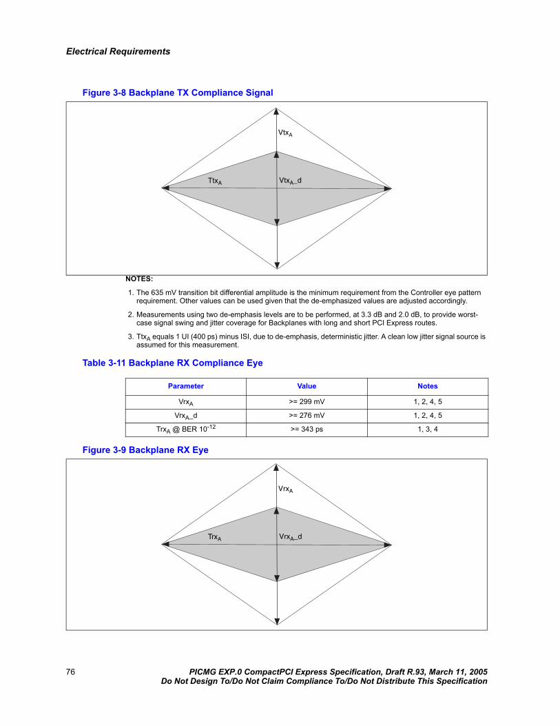
Electrical Requirements
Figure 3-8 Backplane TX Compliance Signal
NOTES:
1. The 635 mV transition bit differential amplitude is the minimum requirement from the Controller eye pattern requirement. Other values can be used given that the de-emphasized values are adjusted accordingly.
2. Measurements using two de-emphasis levels are to be performed, at 3.3 dB and 2.0 dB, to provide worst-case signal swing and jitter coverage for Backplanes with long and short PCI Express routes.
3. TtxA equals 1 UI (400 ps) minus ISI, due to de-emphasis, deterministic jitter. A clean low jitter signal source is assumed for this measurement.
Table 3-11 Backplane RX Compliance Eye
Figure 3-9 Backplane RX Eye
TtxA
VtxA
VtxA_d
Parameter Value Notes
VrxA >= 299 mV 1, 2, 4, 5
VrxA_d >= 276 mV 1, 2, 4, 5
TrxA @ BER 10-12 >= 343 ps 1, 3, 4
TrxA
VrxA
VrxA_d
76 PICMG EXP.0 CompactPCI Express Specification, Draft R.93, March 11, 2005Do Not Design To/Do Not Claim Compliance To/Do Not Distribute This Specification

Electrical Requirements
NOTES:
1. An ideal source without jitter is assumed for this specification.
2. Transition and nontransition bits shall be distinguished to measure compliance against the de-emphasized voltage level (VrxA_d). VrxA and VrxA_d are minimum differential peak-to-peak output voltages.
3. TrxA is the minimum eye width. The eye diagram is defined and centered with respect to the jitter median. This budget allocates 10 psec to jitter introduced from crosstalk between differential signals. From the interconnect jitter budget, 57 psec (90 psec – RXjitter – TXjitter – 10 psec = 57 psec) is available to the Backplane.
4. The values in Table 3-11 are initially referenced to an ideal 100 Ω differential load. Note that these values are not representative of the minimum Receiver input a plug-in board is required to operate with. Instead, they are intended for compliance testing of a Backplane only. The sensitivity requirements are defined and centered with respect to the jitter median.
5. Measurements using two de-emphasis levels shall be performed, at 3.3 dB and 2.0 dB, to provide worst-case signal swing and jitter coverage for Backplanes with long and/or short PCI Express routes. The Backplane RX Eye height parameters, with and without de-emphasis, must be adjusted based on any adjustments made to the source parameters defined in Table 3-10.
3.1.1.5.10 Alternative Controller TX Measurement
It is not always possible to measure the System Controller Transmitter Path Eye Diagram with an ideal reference clock. In this case, a two-Port measurement may suffice to adjust the measurement for the nonideal reference clock.
Referring to Figure 3-10 below,
1. xn is the sampled phase jitter on the reference clock at the connector. A first-order high pass with a –3 dB frequency of 1.5 MHz is used to measure the reference clock phase jitter.
2. hn is the impulse response of the Transmitter PLL on the System Board.
3. nn is the intrinsic Transmitter jitter assuming an ideal reference clock. The peak-peak value of the total jitter must meet the eye requirements as Table 3-7 specifies.
4. Jn = [xn hn] + nn is the sampled total jitter of the Transmitter and circuit board at Backplane, where is the discrete convolution operator. A first-order high pass clock recovery Function with a –3 dB frequency of 1.5 MHz is used to measure the phase jitter of totaln.
The intrinsic jitter of the Transmitter is then calculated in the discrete time domain by the following formula:
nn = Jn – [xn hn]
where xn is convolved with hn. The peak-peak value of nn is then calculated.
This single equation has two unknowns, hn and nn. If hn is known, it can be used directly. Otherwise, hn must be assumed to be the lowest limit of the allowed PLL bandwidth with no peaking (see the PCI Express Base Specification, version 1.1, for the PLL bandwidth limits).
A summary of this procedure is:
1. Take the simultaneous measurements of Jn and xn for the System Board at the connector.
2. Find xn hn.
3. Calculate nn = Jn – [xn hn]
4. Calculate the peak-peak value of nn.
⊗⊗
⊗
⊗⊗
PICMG EXP.0 CompactPCI Express Specification, Draft R.93, March 11, 2005 77Do Not Design To/Do Not Claim Compliance To/Do Not Distribute This Specification

Electrical Requirements
Figure 3-10 Alternative Controller Measurement
3.1.1.6 Reference Clock
To reduce jitter, control radiated emissions, and crosstalk, and allow for future silicon fabrication process changes, a low-voltage-swing differential clock is being used, as shown in Section 3.1.1.6.6.
The reference clock is sourced from the System Board and received by a Peripheral Board and/or the Upstream Port of a Switch Board. It is also sourced from the Switch Board and received by the Peripheral Boards and/or Switch Boards connected to its Downstream ports.
Links provided from the System Board and Switch Boards shall be accompanied by a 100 MHz reference clock, dedicated to that Link, to allow for point-to-point connection with Downstream Peripheral Slots, Switches, and Switch Boards.
Signal parameters follow that of standard LVPECL (Low Voltage Positive Emitter Coupled Logic) for driving onto the Backplane. Other logic families that meet the signal swing, rise/fall time, phase jitter and other requirements provided within this chapter are allowed.
Section 3.1.1.6.7 provides a reference clock phase jitter specification, which shall be met independently of the source of this clock and any fan-out requirements.
Any Device designed onto a board or proprietary Backplane implementation, and receiving the reference clock from the Backplane, shall include AC-coupling, as Section 3.1.1.6.4 describes. The Device also shall include biasing for converting the signal to that appropriate for the receiving PCI Express Device. The chapter on AC-coupling provides a recommended biasing network, although the board designer must guarantee that signal integrity parameters are met.
3.1.1.6.1 Hot-Plug
Clock sources may provide “clock disable” functionality to allow clocks to unused slots to be inactive. This reduces or prevents EMI from unterminated clock signals. However, a system design shall pass compliance assuming all clock signals are active, independent of whether a particular slot is populated.
Peripheral Boards supporting hot insertion or removal should provide a clock disable mechanism, either through tri-state or forced to a static inactive level, to prevent damage of any unpowered PCI Express Component. MPWRGD may be used to control the clock enabling and disabling. Any such clock disable mechanism shall be implemented to have minimal impact on phase jitter.
h(t) +x(t) h(t)
n(t)
x(t)
X
FromReference
Clock
Total Jitter atConnector
ReferenceClock Jitter at
Connector
⊗ x(t) h(t) + n(t)⊗
78 PICMG EXP.0 CompactPCI Express Specification, Draft R.93, March 11, 2005Do Not Design To/Do Not Claim Compliance To/Do Not Distribute This Specification
Electrical Requirements
3.1.1.6.2 Clock Fan-Out
Connection with a large number of PCI Express capable Peripheral Slots generally requires the addition of a PCI Express Switch, either as a standard board or proprietary implementation, to provide the necessary fan-out. With this fan-out of the PCI Express tree, duplicates of the reference clock must be generated for maintaining a point-to-point connection and signal integrity.
Fan-out of the reference clock shall be accomplished through LVPECL or similar Device(s). LVPECL Devices operate from a commonly available power rail and, if implemented properly, have extremely low additive phase jitter.
All reference clock phase jitter requirements in this specification shall be met with and without a fan-out Device.
3.1.1.6.3 Clocking Dependencies
Master–Slave implementations of this specification (a system controller with one or more Peripheral Boards) using PCI Express Components designed for mainstream markets have specific clocking requirements. The Ports on the two ends of a Link must transmit data at a rate within 600 parts per million (PPM) of each other at all times. This is specified to allow bit rate clock sources with a ±300 PPM tolerance.
Compute engine designs targeting Type 1 Peripheral Slots, in addition to the System Slot, shall provide control not to drive the reference clocks onto the Backplane when installed in a Peripheral Slot. Support of such architecture requires monitoring of the SYSEN# pin. It must be based on this configure itself either to drive the reference clocks onto the Backplane, when inserted into a System Slot, or receive a clock when inserted into a Type 1 Peripheral Slot.
3.1.1.6.3.1 Spread Spectrum Clock (SSC) Sources
The data rate can be modulated from +0% to –0.5% of the nominal data rate frequency, at a modulation rate in the range not exceeding 30 kHz–33 kHz. The ±300 PPM requirement still holds, which requires the two communicating Ports be modulated such that they never exceed a total of 600 PPM difference. For most implementations, this places the requirement that both Ports of a Link require the same reference clock source when the data is modulated with an SSC.
Any board design targeting this specification shall support SSC.
3.1.1.6.4 AC-Coupling and Biasing
The Reference Clock shall be AC-Coupled at the board receiving the differential clock. A recommended value is 0.1 uF, although other capacitor values are allowed within the signal integrity and rise/fall time specifications provided in Section 3.1.1.6.6.
Appropriate biasing is required, following the AC-Coupling, for meeting the input requirements of the PCI Express Component designed onto the Peripheral Board. Figure 3-11 and Figure 3-12 provide suggestions for termination of LVPECL signaling, converting the DC bias levels to that compliant with mainstream PCI Express Components.
PICMG EXP.0 CompactPCI Express Specification, Draft R.93, March 11, 2005 79Do Not Design To/Do Not Claim Compliance To/Do Not Distribute This Specification
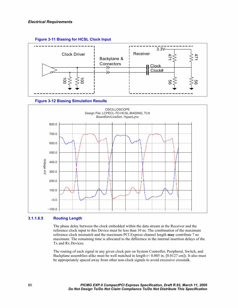
Electrical Requirements
Figure 3-11 Biasing for HCSL Clock Input
Figure 3-12 Biasing Simulation Results
3.1.1.6.5 Routing Length
The phase delay between the clock embedded within the data stream at the Receiver and the reference clock input to this Device must be less than 10 ns. The combination of the maximum reference clock mismatch and the maximum PCI Express channel length may contribute 7 ns maximum. The remaining time is allocated to the difference in the internal insertion delays of the Tx and Rx Devices.
The routing of each signal in any given clock pair on System Controller, Peripheral, Switch, and Backplane assemblies alike must be well matched in length (< 0.005 in. [0.0127 cm]). It also must be appropriately spaced away from other non-clock signals to avoid excessive crosstalk.
Connectors
Clock Driver Receiver
Clock
5656Clock#
Backplane &
471
471
100
100
3.3V
800.0
700.0
600.0
500.0
400.0
300.0
200.0
100.0
–0.0
–100.0
Voltage m
V
OSCILLOSCOPEDesign File: LCPECL-TO-HCSL-BIASING, TLN
BoardSim/LineSim, HyperLynx
80 PICMG EXP.0 CompactPCI Express Specification, Draft R.93, March 11, 2005Do Not Design To/Do Not Claim Compliance To/Do Not Distribute This Specification

Electrical Requirements
Routing length of the reference clock differential pairs on boards shall be greater than 2 in. [5.08 cm] and not exceed 4 in. [10.16 cm].
Assuming a maximum PCI Express trace length of 20 in. [50.8 cm], reference clock routes implemented on the Backplane shall be matched in length within 5 in. [12.7 cm]. This matching requirement can be relaxed with shorter PCI Express trace lengths. No specific minimum or maximum trace length is implied.
3.1.1.6.6 Reference Clock Specification
The following tables provide the signaling requirements at the connectors for the clock source and the worst-case differential signaling a Receiver should expect.
Table 3-12 Reference Clock Source AC Timing
Symbol Parameter100 MHz Input
Unit NoteMin Max
Rise Edge Rate Rising Edge Rate 2.0 6.0 V/ns 2, 3
Fall Edge Rate Falling Edge Rate 2.0 6.0 V/ns 2, 3
VOH Differential Output High Voltage
+250 mV 2, 3
VOL Differential Output Low Voltage
–250 mV 2, 3
VIH Differential Input High Voltage
+200 mV 2, 3
VIL Differential Input Low Voltage
–200 mV 2, 3
VDIFF MAX Maximum differential amplitude
+2100 mV 1, 4
VCROSS DELTA Variation of VCROSS over all rising clock edges
+140 mV 1, 4, 8
VRB Ringback Voltage Margin –200 +200 mV 2, 11
TSTABLE Time before VRB is allowed 500 ps 2, 11
TPERIOD AVG Average Clock Period Accuracy
–300 +2800 PPM 2, 9, 12
TPERIOD ABS Absolute Period (including Jitter and Spread
Spectrum)
9.847 10.203 ns 2, 5
TCCJITTER Cycle to Cycle jitter 150 ps 2
TPHASEJITTER Phase Jitter 80 ps 10
VSWING MAX Absolute Max output swing +1.05 V 1, 6
VSWING MIN Absolute Min output swing +0.25 V 1, 7
VSYM Symmetry of signal swing and level
10 % 1
PICMG EXP.0 CompactPCI Express Specification, Draft R.93, March 11, 2005 81Do Not Design To/Do Not Claim Compliance To/Do Not Distribute This Specification

Electrical Requirements
NOTES:
1. Measurement taken from single-ended waveform.
2. Measurement taken from differential waveform.
3. Measured from VOH / VOL and VIH / VIL on the differential waveform (derived from REFCLK+ minus REFCLK-). The signal must be monotonic through the measurement region for rise and fall time. The 500 mV/400 mV measurement window, of the clock source and Receiver respectively, is centered on the differential zero crossing. See Figure 3-17.
4. Measured at crossing point where the instantaneous voltage value of the rising edge of REFCLK+ equals the falling edge of REFCLK–. See Figure 3-14.
5. Defined as the absolute minimum or maximum instantaneous period. This includes cycle to cycle jitter, relative PPM tolerance, and spread spectrum modulation. See Figure 3-16.
6. Defined as the maximum voltage swing. See Figure 3-13.
7. Defined as the minimum voltage swing. See Figure 3-13.
8. Defined as the total variation of all crossing voltages of Rising REFCLK+ and Falling REFCLK–. This is the maximum allowed variance in VCROSS for any particular system. See Figure 3-14.
9. Refer to Section 4.3.2.1 of the PCI Express Base Specification for information regarding PPM considerations.
10.System Board compliance measured at the Peripheral card connector using the circuit of Figure 3-11. REFCLK+ and REFCLK– are to be measured at the load capacitors CL. Single-ended probes must be used for measurements requiring single-ended measurements. Either single-ended probes with math or differential probe can be used for differential measurements. Test load CL = 2 pF. Phase jitter requirements are provided in Section 3.1.1.6.7.
11.TSTABLE is the time the differential output clock must maintain a minimum ±250 mV differential voltage after rising/falling edges before it is allowed to droop back into the VRB ±200 mV differential range. See Figure 3-18.
12.PPM refers to parts per million and is a DC absolute period accuracy specification. 1 PPM is 1/1,000,000th of 100.000000 MHz exactly or 100 Hz. For 300 PPM, we have an error budget of 100 Hz/PPM * 300 PPM = 30 kHz. The period is to be measured with a frequency counter with measurement window set to 100 ms or greater. The ±300 PPM applies to systems that do not employ Spread Spectrum or that use common clock source. For systems employing Spread Spectrum, there is an additional 2500 PPM nominal shift in maximum period resulting from the 0.5% down spread, resulting in a maximum average period specification of +2800 PPM.
13.Matching applies to rising edge rate for REFCLK+ and falling edge rate for REFCLK–. It is measured using a ±75 mV window centered on the median cross point where REFCLK+ rising meets REFCLK- falling. The median cross point is used to calculate the voltage thresholds the oscilloscope is to use for the edge rate calculations. The Rise Edge Rate of REFCLK+ should be compared to the Fall Edge Rate of REFCLK–. The maximum allowed difference should not exceed 20% of the slowest edge rate. See Figure 3-15.
Duty Cycle Duty Cycle 40 60 % 2
Rise-Fall Matching
Rising edge rate (REFCLK+) to falling edge rate (REFCLK–) matching
20 % 1, 13
ZC-DC Clock source DC impedance
40 60 Ω 1,10
Symbol Parameter100 MHz Input
Unit NoteMin Max
82 PICMG EXP.0 CompactPCI Express Specification, Draft R.93, March 11, 2005Do Not Design To/Do Not Claim Compliance To/Do Not Distribute This Specification

Electrical Requirements
Figure 3-13 Single-Ended Measurement for Swing
Figure 3-14 Single-Ended Measurement Points for Delta Cross Point
Figure 3-15 Single-Ended Measurement Points for Rise and Fall Time Matching
Figure 3-16 Differential Measurement Points for Duty Cycle and Period
Vcross min = -70mV
Clock#
Clock
Voh / Vih
Vol / Vil
Vcross max = 70mV0V
Clock#
Clock
Vcross delta = 140mV Vcross delta = 140mV
Vcross median
Clock
Clock#
Vcross
Clock
Clock#
Vcross +75mV
Vcross -75mV
TfallTrise
0.0V
Positive Duty Cycle (Differential )
0.0V
Negative Duty Cycle (Differential )
Clock / Clock#
Clock Period (Differential )
PICMG EXP.0 CompactPCI Express Specification, Draft R.93, March 11, 2005 83Do Not Design To/Do Not Claim Compliance To/Do Not Distribute This Specification
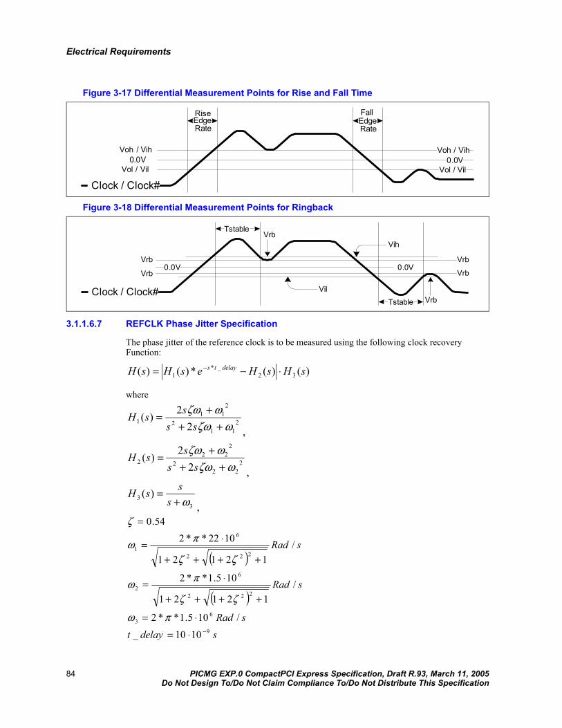
Electrical Requirements
Figure 3-17 Differential Measurement Points for Rise and Fall Time
Figure 3-18 Differential Measurement Points for Ringback
3.1.1.6.7 REFCLK Phase Jitter Specification
The phase jitter of the reference clock is to be measured using the following clock recovery Function:
where
,
,
,
Voh / Vih0.0V
RiseEdgeRate
Clock / Clock#Vol / Vil
Voh / Vih0.0V
Vol / Vil
FallEdgeRate
Vrb
Vil
Vih
Tstable
Tstable
Clock / Clock#
0.0VVrb
0.0VVrb
Vrb
Vrb
Vrb
)()(*)()( 32_*
1 sHsHesHsH delayts ⋅−= −
211
2
211
1 22
)(ωζω
ωζω++
+=
sss
sH
222
2
222
2 22)(
ωζωωζω++
+=
ssssH
33 )(
ω+=
sssH
( )
( )
sdelayt
sRad
sRad
sRad
9
63
222
6
2
222
6
1
1010_
/105.1**2
/12121
105.1**2
/12121
1022**254.0
−⋅=
⋅=
++++
⋅=
++++
⋅=
=
πω
ζζ
πω
ζζ
πω
ζ
84 PICMG EXP.0 CompactPCI Express Specification, Draft R.93, March 11, 2005Do Not Design To/Do Not Claim Compliance To/Do Not Distribute This Specification

Electrical Requirements
Table 3-13 gives the maximum allowed magnitude of the peak-to-peak reference clock phase jitter. For information about the maximum peak-to-peak phase jitter value, see the respective white paper available from the PCI-SIG. There are multiple methods for measuring the maximum allowed peak-to-peak phase jitter value. Real-time sampling scopes must use a sampling rate of 20 Gsamples/s or better and take enough data to guarantee the proper bit error rate (BER). Reference clock measurements for Peripheral Boards shall be taken, with a differential high-impedance probe, using the circuit in Figure 3-11 at the load capacitors CL.
Table 3-13 Maximum Allowed Phase Jitter
3.1.2 ESDAll signal and power pins shall withstand 2000 V of ESD using the human body model and 500 V using the charged Device model without damage. Class 2 per JEDEC JESE22-A114-A.
3.1.3 5 Vaux 5 Vaux is available soon after AC power is applied to a CompactPCI Express system as well as before, during, and after the main DC outputs are enabled. 5 Vaux shall be available in CompactPCI Express systems that support Hot-Plug. It shall be used by boards supporting Hot-Plug and any of the following: SMBus, SMBus ALERT#, or WAKE# for precharge voltage purposes.
Systems not supporting 5 Vaux shall tie this pin to the main 5 V power rail and shall leave the PWRBTN# unconnected at the System Slot. System Boards shall power up and power down properly in systems with or without 5 Vaux support. This may be achieved by reconfiguring the System Board in some way to indicate which type of system it is being used in.
System Boards may use 5 Vaux to maintain the on/off state of the system based on the PWRBTN# signal.
In some circuits requiring auxiliary power, 3.3 Vaux is needed. To make use of mainstream power supplies without needing additional regulators on the Backplane, only 5 Vaux is available. Boards that need 3.3 Vaux should create it locally by regulating down from 5 Vaux.
3.1.4 SMBusThe SMBus interface is Optional for Peripheral Boards and required for System Boards and shares the same pins that can be Optionally used for IPMI. The SMBus consists of a data line called SMBDAT, a clock line called SMBCLK, and an interrupt line called ALERT#.
To allow for a 21 slots and one Backplane Device to have SMBus capability and up to 20 in. of Backplane trace routing without adding repeater Devices, there shall be a SMBus buffer Device on System Boards that has 2 mA rise time accelerator capability. The specification of the Pull-Up value relies on the SMBus Device having the rise time accelerator capability. Peripheral Boards that use the SMBus may have SMBus rise time accelerator capability.
BER Maximum Peak—Peak Phase Jitter Value (ps)
10-6 86
10-12 108
PICMG EXP.0 CompactPCI Express Specification, Draft R.93, March 11, 2005 85Do Not Design To/Do Not Claim Compliance To/Do Not Distribute This Specification

Electrical Requirements
A 3.3 KΩ ±10% Pull-Up resistor to 5 Vaux shall be used on the SMBDAT and SMBCLK on System Boards. System Boards that can operate in Peripheral Slots shall disconnect the Pull-Ups when operating in Peripheral Slots. The Pull-Up resistor is based on the capacitance budgets listed in Table 3-14.
Table 3-14 Capacitance Budgets for SMBus, ALERT, and WAKE# Signals
Table 3-15 lists the DC electrical requirements for the SMBus that CompactPCI Express Boards and Backplanes shall meet.
Table 3-15 DC Electrical Requirements for the SMBus
Backplane Capacitance Budget
21 male ADF connectors at 1.5 pF each 31 pF
21 through-holes for ADF connectors at 1.5 pF each 31 pF
20 in. stripline trace at 6 pF/in. 120 pF
Total Capacitance for Backplane 182 pF
Board Capacitance Budget
Female ADF connector 2 pF
Through-hole for ADF connector 1.5 pF
Via 0.5 pF
2.5 in. stripline trace 15 pF
I2C Device 10 pF
Total for 21 Boards plus one Backplane Device 635 pF
Total Capacitance Budget for System 817 pF
Symbol ParameterLimits
Units CommentsMin Max
VIL SMBus signal Input low voltage — 0.8 V
VIH SMBus signal Input high voltage 2.1 VDD V
VOL SMBus signal Output low voltage — 0.4 V @IPULLUP
ILEAK-BUS Input Leakage per bus segment ±200 uA
ILEAK-PIN Input Leakage per Device pin ±10 uA
VDD Nominal bus voltage 4.75 5.25 V 5 V ±5%
IPULLUP Current sinking, VOL = 0.4 V 3 mA
CBUS Capacitive load of SMBus for entire system
817 pF
CBP Capacitive load of Backplane PCB including Backplane male
connectors
182 pF
86 PICMG EXP.0 CompactPCI Express Specification, Draft R.93, March 11, 2005Do Not Design To/Do Not Claim Compliance To/Do Not Distribute This Specification
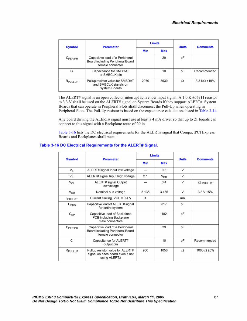
Electrical Requirements
The ALERT# signal is an open collector interrupt active low input signal. A 1.0 K ±5% Ω resistor to 3.3 V shall be used on the ALERT# signal on System Boards if they support ALERT#. System Boards that can operate in Peripheral Slots shall disconnect the Pull-Up when operating in Peripheral Slots. The Pull-Up resistor is based on the capacitance calculations listed in Table 3-14.
Any board driving the ALERT# signal must use at least a 4 mA driver so that up to 21 boards can connect to this signal with a Backplane route of 20 in.
Table 3-16 lists the DC electrical requirements for the ALERT# signal that CompactPCI Express Boards and Backplanes shall meet.
Table 3-16 DC Electrical Requirements for the ALERT# Signal.
CPERIPH Capacitive load of a Peripheral Board including Peripheral Board
female connector
29 pF
CI Capacitance for SMBDAT or SMBCLK pin
10 pF Recommended
RPULLUP Pullup resistor value for SMBDAT and SMBCLK signals on
System Boards
2970 3630 Ω 3.3 KΩ ±10%
Symbol ParameterLimits
Units CommentsMin Max
Symbol ParameterLimits
Units CommentsMin Max
VIL ALERT# signal Input low voltage — 0.8 V
VIH ALERT# signal Input high voltage 2.1 VDD V
VOL ALERT# signal Output low voltage
— 0.4 V @IPULLUP
VDD Nominal bus voltage 3.135 3.465 V 3.3 V ±5%
IPULLUP Current sinking, VOL = 0.4 V 4 mA
CBUS Capacitive load of ALERT# signal for entire system
817 pF
CBP Capacitive load of Backplane PCB including Backplane
male connectors
182 pF
CPERIPH Capacitive load of a Peripheral Board including Peripheral Board
female connector
29 pF
CI Capacitance for ALERT# output pin
10 pF Recommended
RPULLUP Pullup resistor value for ALERT# signal on each board even if not
using ALERT#
950 1050 Ω 1000 Ω ±5%
PICMG EXP.0 CompactPCI Express Specification, Draft R.93, March 11, 2005 87Do Not Design To/Do Not Claim Compliance To/Do Not Distribute This Specification

Electrical Requirements
3.1.4.1 SMBus “Back Powering” Considerations
Unpowered Devices connected to a SMBus segment shall provide, either within the Device or through the interface circuitry, protection against “back powering” the SMBus. Unpowered Devices must not exceed ±5 uA leakage current.
3.1.4.2 Backplane Identification and Capability Using SMBus
This specification supports two different ways to route the System Slot, several Link widths, and several different slot types that a Chassis designer can choose from when developing a Backplane. This makes it difficult for integrators, manufacturers, and customers to understand the total system (Backplane plus System Board) capability. This section details descriptors for communicating the interface type, slot type, and interface throughput (speed and width) of each slot in a Backplane. With these descriptors, System Board vendors can create an application that can communicate the system’s various capabilities to the user. The System Board and Backplane contain an SMBus for reading the Backplane Capability Record. The capability record is rich enough to describe different interfaces (PCI, PCI-Express Gen 1, Advanced Switching, etc.). The Backplane Capability Record also allows for unique identification of the Backplane.
Terms used in this section:
Slot Number or Slot—The Physical Slot number silkscreened on a Backplane representing the Physical Slot Number.
Link Number or Link—The Link number specified in the pin definition for the given slot type. For example, the 4-Link System Slot contains Links 1 through 4, identified in the pin definition in Table 3-28.
The Backplane Capability Record format includes the Backplane Descriptor shown in Table 3-17, the System Slot Descriptor shown in Table 3-18, and one Peripheral Slot Descriptor shown in Table 3-19 for each Peripheral Slot.
Table 3-17 Backplane Descriptor
Byte Offset Name Description
0:2 PID PICMG ID—A 3 byte ID assigned to PICMG. For all records defined in this specification, a value of 12634 (00315 Ah) shall be used. This value is stored LS-Byte at the lowest byte address.
3 PRI PICMG Record ID—Indicates a Backplane Descriptor (04 h)
4 RFV Record Format Version—Shall be 0 for this Backplane Descriptor version.
5:64 VID Vendor ID—A 60 byte string indicating the vendor of the Backplane. This 60 bytes includes a Null terminator. The string starts at the lowest byte address.
64:103 MOD Model—A 40 byte string indicating the Backplane model. This 40 bytes includes a Null terminator. The string starts at the lowest byte address.
104 REV Revision—An ASCII byte representing the Backplane revision.
105:117 SN Serial Number—A 13 byte string indicating the Backplane serial number. The 13 bytes includes a Null terminator. The string starts at the lowest byte address.
88 PICMG EXP.0 CompactPCI Express Specification, Draft R.93, March 11, 2005Do Not Design To/Do Not Claim Compliance To/Do Not Distribute This Specification

Electrical Requirements
Table 3-18 System Slot Descriptor
118 SC Slot Count—Indicates the total number of Physical Slots (1–31) on the Backplane. This count includes the System Slot and any Switch slots.
119 PSC Peripheral Slot Count—Indicates the number of physical Peripheral Slots (1–30) on the Backplane. This count excludes the System Slot.
120:121 CKSM Checksum—A 2 byte checksum for the entire 256 bytes of the EEPROM excluding the checksum. This value is stored LS-Byte at the lowest byte address.
Byte Offset Name Description
122 SSN System Slot Number—Indicates the number of the Physical Slot (1-31) being described in this descriptor.
123 SST System Slot Type—Indicates whether the System Slot of the Backplane is a 2-Link or 4-Link System Slot.0—2-Link1—4-Link
124 SSL1W System Slot Link 1 Width—Indicates the routed Link width of the PCI Express Link Number 1 of the System Slot.1—x1 Gen 1 PCI Express Signaling2—x4 Gen 1 PCI Express Signaling3—x8 Gen 1 PCI Express Signaling
125 SSL2W System Slot Link 2 Width—Indicates the routed Link width of the PCI Express Link Number 2 of the System Slot.1—x1 Gen 1 PCI Express Signaling2—x4 Gen 1 PCI Express Signaling3—x8 Gen 1 PCI Express Signaling4—x16 Gen 1 PCI Express Signaling
126 SSL3W System Slot Link 3 Width—Indicates the routed Link width of the PCI Express Link Number 3 of the System Slot.0—Indicates this is a 2-Link System Slot.1—x1 Gen 1 PCI Express Signaling2—x4 Gen 1 PCI Express Signaling
127 SSL4W System Slot Link 4 Width—Indicates the routed Link width of the PCI Express Link Number 4 of the System Slot.0—Indicates this is a 2-Link System Slot.1—x1 Gen 1 PCI Express Signaling2—x4 Gen 1 PCI Express Signaling
Byte Offset Name Description
PICMG EXP.0 CompactPCI Express Specification, Draft R.93, March 11, 2005 89Do Not Design To/Do Not Claim Compliance To/Do Not Distribute This Specification
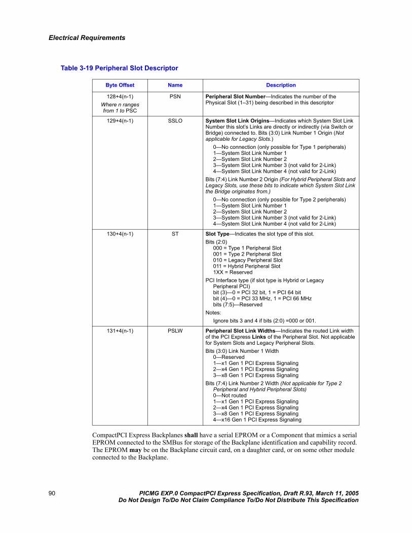
Electrical Requirements
Table 3-19 Peripheral Slot Descriptor
CompactPCI Express Backplanes shall have a serial EPROM or a Component that mimics a serial EPROM connected to the SMBus for storage of the Backplane identification and capability record. The EPROM may be on the Backplane circuit card, on a daughter card, or on some other module connected to the Backplane.
Byte Offset Name Description
128+4(n-1)Where n ranges from 1 to PSC
PSN Peripheral Slot Number—Indicates the number of the Physical Slot (1–31) being described in this descriptor
129+4(n-1) SSLO System Slot Link Origins—Indicates which System Slot Link Number this slot’s Links are directly or indirectly (via Switch or Bridge) connected to. Bits (3:0) Link Number 1 Origin (Not applicable for Legacy Slots.)
0—No connection (only possible for Type 1 peripherals) 1—System Slot Link Number 12—System Slot Link Number 23—System Slot Link Number 3 (not valid for 2-Link)4—System Slot Link Number 4 (not valid for 2-Link)
Bits (7:4) Link Number 2 Origin (For Hybrid Peripheral Slots and Legacy Slots, use these bits to indicate which System Slot Link the Bridge originates from.)
0—No connection (only possible for Type 2 peripherals)1—System Slot Link Number 12—System Slot Link Number 23—System Slot Link Number 3 (not valid for 2-Link)4—System Slot Link Number 4 (not valid for 2-Link)
130+4(n-1) ST Slot Type—Indicates the slot type of this slot.Bits (2:0)
000 = Type 1 Peripheral Slot001 = Type 2 Peripheral Slot010 = Legacy Peripheral Slot011 = Hybrid Peripheral Slot1XX = Reserved
PCI Interface type (if slot type is Hybrid or Legacy Peripheral PCI)bit (3)—0 = PCI 32 bit, 1 = PCI 64 bitbit (4)—0 = PCI 33 MHz, 1 = PCI 66 MHzbits (7:5)—Reserved
Notes:Ignore bits 3 and 4 if bits (2:0) =000 or 001.
131+4(n-1) PSLW Peripheral Slot Link Widths—Indicates the routed Link width of the PCI Express Links of the Peripheral Slot. Not applicable for System Slots and Legacy Peripheral Slots.Bits (3:0) Link Number 1 Width
0—Reserved1—x1 Gen 1 PCI Express Signaling2—x4 Gen 1 PCI Express Signaling3—x8 Gen 1 PCI Express Signaling
Bits (7:4) Link Number 2 Width (Not applicable for Type 2 Peripheral and Hybrid Peripheral Slots)0—Not routed1—x1 Gen 1 PCI Express Signaling2—x4 Gen 1 PCI Express Signaling3—x8 Gen 1 PCI Express Signaling4—x16 Gen 1 PCI Express Signaling
90 PICMG EXP.0 CompactPCI Express Specification, Draft R.93, March 11, 2005Do Not Design To/Do Not Claim Compliance To/Do Not Distribute This Specification

Electrical Requirements
The serial EPROM for the storage of the Backplane identification and capability record shall meet the following requirements:
• The serial EPROM shall connect to the System Slot SMBData and SMBClock signals.
• The serial EPROM shall support signaling rates up to 100 kHz.
• The serial EPROM shall be mapped at address A4h.
• The serial EPROM shall be at least 256 bytes in size.
• The serial EPROM shall support both random address access and automatic increment address access.
• The serial EPROM shall contain the Backplane Identification and Capability Record, which includes one Backplane Descriptor, one System Slot Descriptor, and n Peripheral Slot Descriptors, where n is the Peripheral Slot Count (PSC) listed in the Backplane Descriptor.
• The serial EPROM may be powered from either 5 Vaux or 5 V.
Table 3-20 shows an example of the Backplane identification and capability record for the eight-slot Backplane in Figure 3-19.
Figure 3-19 Eight-Slot Backplane Example
x8 PCIe
x16 PCIe
x4 PCIex8 PCIe
x1 PCIe
x1 PCIe
x4 PCIe
32 bit 33 MHz PCI Bus Seg.
x4 PCIe
x4 PCIe
PCIe toPCI Bridge
PCIeSwitch
PCIeSwitchx8 PCIe
1 2 3 4 5 6 7 8
PICMG EXP.0 CompactPCI Express Specification, Draft R.93, March 11, 2005 91Do Not Design To/Do Not Claim Compliance To/Do Not Distribute This Specification

Electrical Requirements
Table 3-20 Backplane Identification and Capability Record Example
Byte Offset Value Description
Backplane Descriptor
0:2 00315Ah PICMG ID—A 3 byte ID assigned to PICMG. For all records defined in this specification, a value of 12634 (00315Ah) shall be used. This value is stored LS-Byte at the lowest byte address.
3 04h PCIMG Record ID—Indicates a Backplane Descriptor (04h).
4 0 Record Format Version—Shall be 0 for this Backplane Descriptor version.
5:64 “CPCIe Vendor Inc.” Vendor ID—A 60 byte string indicating the Backplane vendor. This 60 bytes includes a Null terminator. The string starts at the lowest byte address.
64:103 “XYZ-123” Model—A 40 byte string indicating the Backplane model. This 40 bytes includes a Null terminator. The string starts at the lowest byte address.
104 43h Revision—An ASCII byte representing the Backplane revision. Revision ‘C’ in this example.
105:117 “000038a2e941” Serial Number—A 13 byte string indicating the Backplane serial number. The 13 bytes includes a Null terminator. The string starts at the lowest byte address.
118 8 Slot Count—Indicates the total number of Physical Slots (1-31) on the Backplane. This count includes the System Slot and any Switch slots.
119 7 Peripheral Slot Count—Indicates the number of physical Peripheral Slots (1-30) on the Backplane. This count excludes the System Slot.
120:121 Not calculated for this example
Checksum—A 2 byte checksum for the entire 256 bytes of the EEPROM excluding the checksum. This value is stored LS-Byte at the lowest byte address.
System Slot Descriptor
122 1 System Slot Number—Slot 1.
123 0 System Slot Type—2-Link.
124 3 System Slot Link 1 Width—x8 Gen 1 PCI Express Signaling.
125 4 System Slot Link 2 Width—x16 Gen 1 PCI Express Signaling.
126 0 System Slot Link 3 Width—Indicates this is a 2-Link System Slot.
127 0 System Slot Link 4 Width—Indicates this is a 2-Link System Slot.
Peripheral Slot Descriptor for Slot 2
128 2 Peripheral Slot Number—Slot 2.
129 21h System Slot Link Origins—Link 1 comes from System Slot Link Number 1, and Link 2 comes from System Slot Link Number 2.
92 PICMG EXP.0 CompactPCI Express Specification, Draft R.93, March 11, 2005Do Not Design To/Do Not Claim Compliance To/Do Not Distribute This Specification

Electrical Requirements
130 00h Slot Type—Type 1 Peripheral Slot.
131 43h Peripheral Slot Link Widths—Link Number 1 Width is x8 Gen 1 PCI Express Signaling, and Link Number 2 Width is x16 Gen 1 PCI Express Signaling.
Peripheral Slot Descriptor for Slot 3
132 3 Perhipheral Slot Number—Slot 3.
133 01h System Slot Link Origins—Link 1 comes from System Slot Link Number 1.
134 01h Slot Type—Type 2 Peripheral Slot.
135 02h Peripheral Slot Link Widths—Link Number 1 Width is x4 Gen 1 PCI Express Signaling.
Peripheral Slot Descriptor for Slot 4
136 4 Perhipheral Slot Number—Slot 4.
137 11h System Slot Link Origins—Link 1 comes from System Slot Link Number 1, and PCI comes from System Slot Link Number 1.
138 03h Slot Type—Hybrid Peripheral Slot with 32 bit 33 MHz PCI.
139 02h Peripheral Slot Link Widths—Link Number 1 Width is x4 Gen 1 PCI Express Signaling.
Peripheral Slot Descriptor for Slot 5
140 5 Perhipheral Slot Number—Slot 5.
141 11h System Slot Link Origins—Link 1 comes from System Slot Link Number 1, and PCI comes from System Slot Link Number 1.
142 03h Slot Type—Hybrid Peripheral Slot with 32-bit 33 MHz PCI.
143 02h Peripheral Slot Link Widths—Link Number 1 Width is x4 Gen 1 PCI Express Signaling.
Peripheral Slot Descriptor for Slot 6
144 6 Perhipheral Slot Number—Slot 6.
145 11h System Slot Link Origins—Link 1 comes from System Slot Link Number 1, and PCI comes from System Slot Link Number 1.
146 03h Slot Type—Hybrid Peripheral Slot with 32-bit 33 MHz PCI
147 02h Peripheral Slot Link Widths—Link Number 1 Width is x4 Gen 1 PCI Express Signaling.
Peripheral Slot Descriptor for Slot 7
148 7 Perhipheral Slot Number—Slot 7.
149 11h System Slot Link Origins— Link 1 comes from System Slot Link Number 1, and PCI comes from System Slot Link Number 1.
150 03h Slot Type—Hybrid Peripheral Slot with 32-bit 33 MHz PCI.
Byte Offset Value Description
PICMG EXP.0 CompactPCI Express Specification, Draft R.93, March 11, 2005 93Do Not Design To/Do Not Claim Compliance To/Do Not Distribute This Specification
Electrical Requirements
3.1.5 PWRBTN# SignalThe PWRBTN# is an input signal to the System Board from a mechanical momentary Switch indicating that the operator of a CompactPCI Express Chassis wants to change the system on/off state. To change the system on/off state, the mechanical momentary Switch transitions the PWRBTN# signal from open-circuit to Ground to open-circuit. System Board circuitry powered directly or indirectly from the 5 Vaux rail or an onboard battery should be used to maintain the on/off state. The System Board should use this on/off state, in turn, to control the PS_ON# signal. Because the PWRBTN# signal is from a mechanical Switch, it should be debounced. Systems that do not support 5 Vaux shall leave the PWRBTN# pin unconnected at the System Slot.
3.1.6 PS_ON# SignalThe PS_ON# signal is an active-low, TTL-compatible signal that allows a System Board to control the power supply in conjunction with features such as soft on/off, Wake on LAN*, wake-on-modem, etc. When PS_ON# is driven to TTL low, the power supply shall turn on the output rails: 12 V, 3.3 V, 5 V, and –12 V (for systems with Hybrid or Legacy Slots). When PS_ON# is driven to TTL high or open-circuited, the DC output rails shall not deliver current and shall be held at zero potential with respect to ground. The PS_ON# signal has no effect on the 5 V Aux output, which is always enabled whenever the AC power is present. This signal shall comply with the characteristics in Table 3-21.
Table 3-21 PS_ON# Signal Characteristics
Figure 3-20 shows and Section 3.4.4 details the timing relationship between the PS_ON# signal being Asserted and the DC power rails turning on.
151 01h Peripheral Slot Link Widths—Link Number 1 Width is x4 Gen 1 PCI Express Signaling.
Peripheral Slot Descriptor for Slot 8
152 8 Perhipheral Slot Number—Slot 8.
153 10h System Slot Link Origins—PCI comes from System Slot Link Number 1.
154 02h Slot Type—Legacy Peripheral Slot with 32-bit 33 MHz PCI.
155 00h Peripheral Slot Link Widths—Link Number 1 Width is x4 Gen 1 PCI Express Signaling.
Byte Offset Value Description
Min Max
VIL, Input Low Voltage 0.0 V 0.8 V
IIL, Input Low Current (Vin = 0.4 V) –1.6 mA
VIH, Input High Voltage (Iin = –200 µA) 2.0 V
VIH open circuit, Iin = 0 5.25 V
94 PICMG EXP.0 CompactPCI Express Specification, Draft R.93, March 11, 2005Do Not Design To/Do Not Claim Compliance To/Do Not Distribute This Specification

Electrical Requirements
Figure 3-20 Power Supply Timing
Note: For Figure 3-20, T1 and T2 are specified in Section 3.4.4, and T3, T4, T5, and T6 are specified in Table 3-22.
3.1.7 PWR_OK SignalThe CompactPCI Express Chassis power supply generates the PWR_OK signal, which indicates all DC power rails are within their regulation limits. This signal shall comply with the characteristics and timing requirements detailed in the ATX12V Power Supply Design Guide, Version 2.0.
PWR_OK is a “power good” signal. It shall be Asserted high by the power supply to indicate the 12 VDC, 5 VDC, and 3.3 VDC outputs are above the under-voltage thresholds listed in Section 3.4.2. Conversely, PWR_OK shall be Deasserted to a low state when the 12 VDC, 5 VDC, or 3.3 VDC output voltage falls below its under-voltage threshold, or when mains power has been removed for a long enough time that power supply operation cannot be guaranteed beyond the power-down warning time. The PWR_OK signal electrical and timing characteristics that shall be met are in Table 3-22 and Figure 3-20.
Table 3-22 PWR_OK Signal Characteristics
~
~~
~
VAC
PS_ON#
PWR_OK
+12V,+5V,+3.3V,|-12V|
T1
T2
T3
T4
T5
T6
95%
10%
Signal type +5 V TTL compatible
Logic level low < 0.4 V while sinking 4 mA
Logic level high Between 2.4 V and 5 V output while sourcing 200 µA
High-state output impedance 1 kΩ from output to common
PWR_OK delay 100 ms < T3 < 500 ms
PWR_OK risetime T4 ≤ 10 ms
AC loss to PWR_OK hold-up time T5 ≤ 16 ms
Power-down warning T6 ≥ 1 ms
PICMG EXP.0 CompactPCI Express Specification, Draft R.93, March 11, 2005 95Do Not Design To/Do Not Claim Compliance To/Do Not Distribute This Specification

Electrical Requirements
3.1.8 WAKE# SignalWAKE# is an open-drain, active low signal that a Peripheral Board drives low to reactivate the CompactPCI Express system’s main power rails and reference clocks. It is required on any Peripheral Board or System Board that supports the Wakeup functionality. The requirements for boards that support the WAKE# functionality are derived from the PCI Express CEM Specification, revision 1.1.
Only Peripheral Boards that support the wake process connect to this pin. If the Peripheral Board has Wakeup capabilities, it shall support the WAKE# Function. Likewise, only System Boards that support the Wakeup Function need to connect to this pin, but if they do, they shall fully support the WAKE# Function. Such systems are not required to support Beacon as a Wakeup mechanism, but are encouraged to support it. If the Wakeup process is used, the 3.3 Vaux supply locally derived on Peripheral Boards from the 5 Vaux supply must be present and used for this Function. The assertion and de-assertion of WAKE# are asynchronous to any system clock. (See Chapter 5 of the PCI Express Base Specification for more details on PCI-compatible Power Management.)
WAKE# may be bussed to all Peripheral Board connectors, forming a single input connection at the System Board Power Management (PM) controller. Also, individual Peripheral Slots may have individual connections to the PM controller of a Backplane Switch.
The asserting and receiving ends of WAKE# shall use auxiliary power (3.3 Vaux derived from the 5 Vaux rail) to revive the Hierarchy. The receiving Device (System Board, Switch, or Switch Board) shall also provide a Pull-Up on WAKE#, with the auxiliary power source supplying the receiving Device’s bias voltage reference in support of Link reactivation. Note that the voltage the System Board uses to terminate the WAKE# signal can be lower than the locally derived 3.3 Vaux, to be compatible with lower voltage processes of the system PM controller. However, all potential drivers of the WAKE# signal must be 3.3 V tolerant.
WAKE# has additional electrical requirements over and above standard open drain signals that, for example, allow it to be shared between Devices that are powered off and those that are powered on using auxiliary power. The additional requirements include careful circuit design to ensure that a voltage applied to the WAKE# signal network never causes damage to a Component, even if that particular Component’s power is not applied.
Additionally, the Device shall ensure that it does not pull WAKE# low, unless WAKE# is being intentionally Asserted in all cases, including when the related Function is in D3cold.
This means that any Component implementing WAKE# shall be designed such that:
• Unpowered WAKE# output circuits are not damaged if a voltage is applied to them from other powered “wire-ORed” sources of WAKE#.
• When power is removed from its WAKE# generation logic, the unpowered output does not present a low impedance path to ground or any other voltage.
These additional requirements ensure that the WAKE# signal network continues to Function properly when a mixture of auxiliary powered and unpowered Components have their WAKE# outputs wire-ORed together. Note that most commonly available open drain and tri-state buffer circuit designs used “as is” do not satisfy the additional circuit design requirements for WAKE#.
Other requirements on the System Board/Peripheral Board designer include:
• Common-ground plane reference between slots/Components attached to the same WAKE# signal.
• Split-voltage power planes (3.3 Vaux vs. 3.3 V) are required.
96 PICMG EXP.0 CompactPCI Express Specification, Draft R.93, March 11, 2005Do Not Design To/Do Not Claim Compliance To/Do Not Distribute This Specification

Electrical Requirements
• If 5.0 Vaux is supplied to one slot in a Chassis, it shall be supplied to all slots in that Chassis other than Legacy Slots.
• If WAKE# is supported on one slot in a Chassis, it shall be supported on all slots in that Chassis other than Legacy Slots.
• 5.0 Vaux voltage supply may be present, even if the Device is not enabled for Wakeup events.
• The system may switch off 3.3 V, 12 V, 5 V, and –12 V at a slot.
• Peripheral Boards can generate the Beacon Wakeup mechanism in addition to using the WAKE# mechanism, although the System Board does not need to support the Beacon.
Note: If the Peripheral Board uses the Beacon mechanism in addition to the WAKE# mechanism, the system may ignore the Beacon.
Peripheral Board designers must be aware of the special requirements that constrain WAKE# and ensure that their Peripheral Boards do not interfere with the proper operation of the WAKE# network. The WAKE# input into the system may de-assert as late as 100 ns after the WAKE# output from the Function de-asserts. (That is, the WAKE# pin must be considered indeterminate for a number of cycles after it has been Deasserted.)
The WAKE# signal is an open-collector active low input signal to the System Board. A 150 Ω resistor to locally derived 3.3 Vaux shall be used on the WAKE# signal on System Boards if they support WAKE#. System Boards that can operate in Peripheral Slots shall disconnect the Pull-Up when operating in Peripheral Slots.
Any board driving the WAKE# signal shall use at least a 24 mA driver so that up to 21 boards can connect to this signal with a Backplane route of 20 in. and still meet the maximum rise time of 100 ns.
Table 3-23 lists the DC electrical requirements for the WAKE# signal that boards supporting the wake functionality shall meet.
Table 3-23 DC Electrical Requirements for the WAKE# Signal.
Symbol ParameterLimits
Units CommentsMin Max
VIL WAKE# signal Input low voltage — 0.8 V
VIH WAKE# signal Input high voltage 2.1 VDD V
VOL WAKE# signal Output low voltage — 0.4 V @IPULLUP
VDD Nominal bus voltage 3.135 3.465 V 3.3 V ±5%
IPULLUP Current sinking, VOL = 0.4 V 24 mA
CBUS Capacitive load of WAKE# for entire system
817 pF
CBP Capacitive load of Backplane PCB including Backplane male connectors
182 pF
CPERIPH Capacitive load of a Peripheral Board including Peripheral Board female connector
29 pF
CI Capacitance for WAKE# output pin 10 pF Recommended
RPULLUP Pullup resistor value for WAKE# signal on System Board.
148.5 151.5 Ω 150 Ω ±1%
PICMG EXP.0 CompactPCI Express Specification, Draft R.93, March 11, 2005 97Do Not Design To/Do Not Claim Compliance To/Do Not Distribute This Specification

Electrical Requirements
Table 3-24 gives the timing requirements that shall be met relating to power, PERST#, REFCLK, and WAKE#
Table 3-24 Sequencing and Reset Signal Timings
NOTES:
1. Any supplied power is stable when it meets the regulation requirements specified for that power supply.
2. A supplied reference clock is stable when it meets the requirements specified for the reference clock. The PERST# signal is Asserted and Deasserted asynchronously with respect to the supplied reference clock.
3. The PERST # signal shall be Asserted within Tfail of any supplied power going out of specification.
4. Measured from WAKE# assertion/deassertion to valid input level at the system PM controller.
Figure 3-21 WAKE Rise and Fall Time Measurement Points
Note: Power Management Controller input switching levels are platform dependent and not set by this specification.
3.1.8.1 Implementation Note
Example WAKE# Circuit Design
The following diagram is an example of how the WAKE# generation logic could be implemented. In this example, multiple PCI Express Functions have their WAKE# signals ganged together and connected to the single WAKE# pin on the CompactPCI Express Peripheral Board connector.
The circuit driving the gate of transistor Q1 isolates the Peripheral Board’s WAKE# network from that of the System Board whenever its power source (VSOURCE) is absent.
Symbol Parameter Min Max Units Notes Figure
TpvPERL Power stable to PERST # inactive
100 ms 1 Figure 3-23
TPERST-clk REFCLK stable before PERST# inactive
100 µs 2 Figure 3-23
TPERST PERST# active time 100 µs Figure 3-24
Tfail Power level invalid to PERST# active
500 ns 3 Figure 3-25
Twkrf WAKE# rise-fall time 100 ns 4 Figure 3-21
TWAKE WAKE# hold time from PERST# inactive
1 ms Figure 3-24
WAKE
WAKE
VIH_PMC1
VIL_PMC1
TWRKF
98 PICMG EXP.0 CompactPCI Express Specification, Draft R.93, March 11, 2005Do Not Design To/Do Not Claim Compliance To/Do Not Distribute This Specification

Electrical Requirements
If the Peripheral Board supplies power to its WAKE# logic with a supply other than the auxiliary supply (that is, it does not support Wakeup from D3cold), all WAKE# sources from the card are isolated from the System Board when the Peripheral Board supply rail is switched off. Peripheral Boards that support Wakeup from D3cold have an auxiliary power source (3.3 Vaux derived from the 5 Vaux) to power the WAKE# logic. This maintains connection of these WAKE# sources to the System Board’s WAKE# signal network even when the Link Hierarchy’s power is switched off.
Figure 3-22 WAKE# Circuit Example
This example assumes that either the 3.3 V or 3.3 Vaux (VSOURCE) powers all WAKE# sources on the Peripheral Board. If WAKE# from D3cold is supported by some, but not all, of the Peripheral Boards’s Functions that generate WAKE#, the Peripheral Board designer must ensure there is separate isolation control for each WAKE# generation power source.
PCI Express Component designers can integrate the “power fail detect” isolation circuitry with their WAKE# output pin physically corresponding to the source of FET Q1. Alternately, all isolation control logic could be implemented externally on the Peripheral Boards.
This example is meant as a conceptual aid. It is not intended to prescribe an actual implementation.
3.1.9 PERST# SignalThe PERST# signal indicates when the 3.3 V, 5 V, and 12 V power rails are within its specified voltage tolerance and are stable. It also initializes a Component’s state machines and other logic when power supplies stabilize. On power up, the deassertion of PERST# shall be delayed 100 ms
7407
+-
LT1112_A0
7407
7407
R1
R2
R3
Q2
Q1R4
U1
U1
U1
U2
VSOURCE+
WAKE#
3.3Vaux
Board WAKE# Source n
Board WAKE# Source 2
Board WAKE# Source 1
Peripheral Board System Board
Q1 = FETQ2 = Zener DiodeU1 = Open Drain BufferU2 = ComparatorVSOURCE = Voltage source for WAKE #
logic derived from 5VAux
3.3Vaux = Auxiliary voltage derived from 5Vaux supplied to the board from the backplane
PICMG EXP.0 CompactPCI Express Specification, Draft R.93, March 11, 2005 99Do Not Design To/Do Not Claim Compliance To/Do Not Distribute This Specification
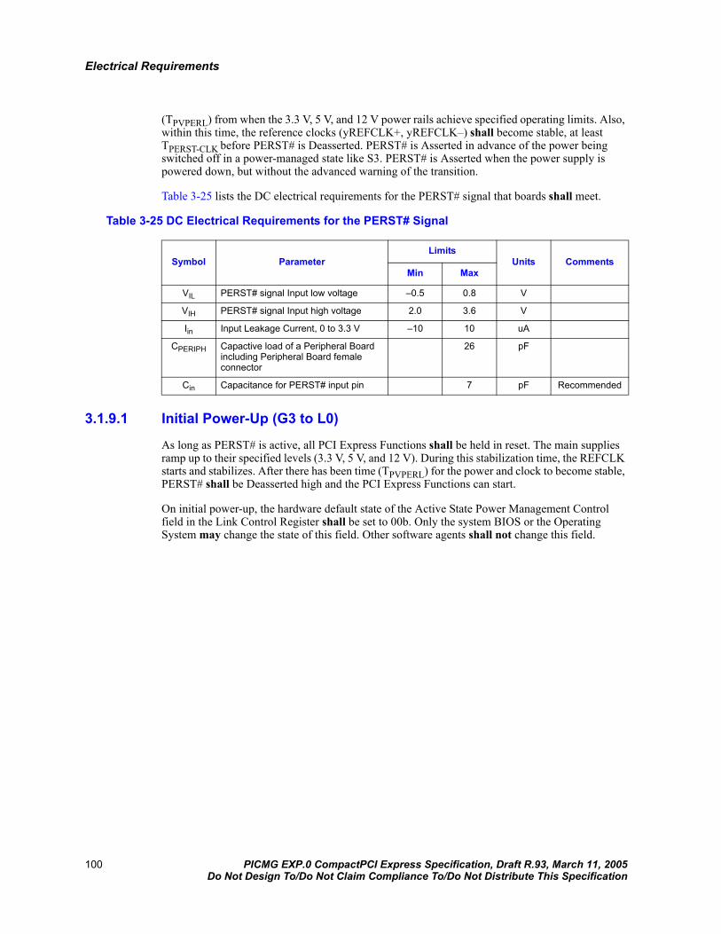
Electrical Requirements
(TPVPERL) from when the 3.3 V, 5 V, and 12 V power rails achieve specified operating limits. Also, within this time, the reference clocks (yREFCLK+, yREFCLK–) shall become stable, at least TPERST-CLK before PERST# is Deasserted. PERST# is Asserted in advance of the power being switched off in a power-managed state like S3. PERST# is Asserted when the power supply is powered down, but without the advanced warning of the transition.
Table 3-25 lists the DC electrical requirements for the PERST# signal that boards shall meet.
Table 3-25 DC Electrical Requirements for the PERST# Signal
3.1.9.1 Initial Power-Up (G3 to L0)
As long as PERST# is active, all PCI Express Functions shall be held in reset. The main supplies ramp up to their specified levels (3.3 V, 5 V, and 12 V). During this stabilization time, the REFCLK starts and stabilizes. After there has been time (TPVPERL) for the power and clock to become stable, PERST# shall be Deasserted high and the PCI Express Functions can start.
On initial power-up, the hardware default state of the Active State Power Management Control field in the Link Control Register shall be set to 00b. Only the system BIOS or the Operating System may change the state of this field. Other software agents shall not change this field.
Symbol ParameterLimits
Units CommentsMin Max
VIL PERST# signal Input low voltage –0.5 0.8 V
VIH PERST# signal Input high voltage 2.0 3.6 V
Iin Input Leakage Current, 0 to 3.3 V –10 10 uA
CPERIPH Capactive load of a Peripheral Board including Peripheral Board female connector
26 pF
Cin Capacitance for PERST# input pin 7 pF Recommended
100 PICMG EXP.0 CompactPCI Express Specification, Draft R.93, March 11, 2005Do Not Design To/Do Not Claim Compliance To/Do Not Distribute This Specification
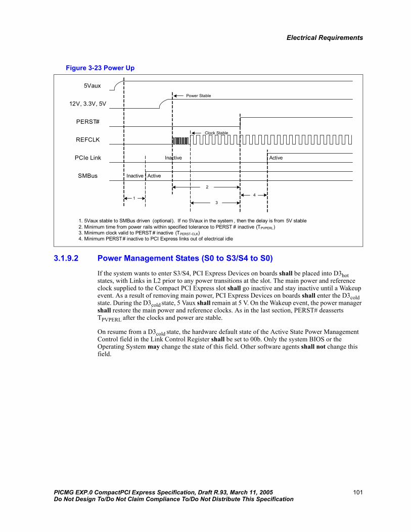
Electrical Requirements
Figure 3-23 Power Up
3.1.9.2 Power Management States (S0 to S3/S4 to S0)
If the system wants to enter S3/S4, PCI Express Devices on boards shall be placed into D3hot states, with Links in L2 prior to any power transitions at the slot. The main power and reference clock supplied to the Compact PCI Express slot shall go inactive and stay inactive until a Wakeup event. As a result of removing main power, PCI Express Devices on boards shall enter the D3cold state. During the D3cold state, 5 Vaux shall remain at 5 V. On the Wakeup event, the power manager shall restore the main power and reference clocks. As in the last section, PERST# deasserts TPVPERL after the clocks and power are stable.
On resume from a D3cold state, the hardware default state of the Active State Power Management Control field in the Link Control Register shall be set to 00b. Only the system BIOS or the Operating System may change the state of this field. Other software agents shall not change this field.
5Vaux
12V, 3.3V, 5V
PERST#
REFCLK
PCIe Link
SMBus Inactive Active
Inactive Active
1
2
3
4
Power Stable
Clock Stable
1. 5Vaux stable to SMBus driven (optional). If no 5Vaux in the system , then the delay is from 5V stable2. Minimum time from power rails within specified tolerance to PERST # inactive (TPVPERL)3. Minimum clock valid to PERST # inactive (TPERST-CLK)4. Minimum PERST# inactive to PCI Express links out of electrical idle
PICMG EXP.0 CompactPCI Express Specification, Draft R.93, March 11, 2005 101Do Not Design To/Do Not Claim Compliance To/Do Not Distribute This Specification

Electrical Requirements
Figure 3-24 Power Management States
3.1.9.3 Power Down
A power rail (12 V, 3.3 V, 5 V, or 5 Vaux) is valid or stable if the specified power rail is within the associated voltage tolerances defined in Table 3-39. Once a power rail is stable, an invalid or unstable power rail is defined as a power rail that has dropped below the specified minimum voltage levels (for example, below 3.135 V for the 3.3 V rails). For purposes of detecting an out-of-tolerance power source, the threshold for detection shall be established in a window range. This range is no more than 500 mV below the specified minimum voltage level for the 3.3 V, 5 Vaux, and 5 V rails (that is, 2.635 V, 4.25 V, and 4.25 V, respectively) and 1.1 V below for the 12 V rail (that is, 10.3 V). Figure 3-25 shows the power down timing.
4
12V, 3.3V, 5V
PWREN#
MPWRGD
PERST#
REFCLK
PCI Express link
SMBus
1
1. PCI Express link goes to idle prior to PERST# going active2. REFCLK goes inactive after PERST# goes active
4. Wakeup event or WAKE# goes active causing power to return then PWREN# goesactive, restarts REFCLK and PERST# goes inactive as in power up sequences.
Active
5 Vaux
WAKE
Active Active
2
3. PWREN# goes inactive after REFCLK goes inactive
3
5
5. Minimum active time for PERST# is T PERST
6
6. Maximum hold time for WAKE# from PERST# inactive is TWAKE
#
102 PICMG EXP.0 CompactPCI Express Specification, Draft R.93, March 11, 2005Do Not Design To/Do Not Claim Compliance To/Do Not Distribute This Specification
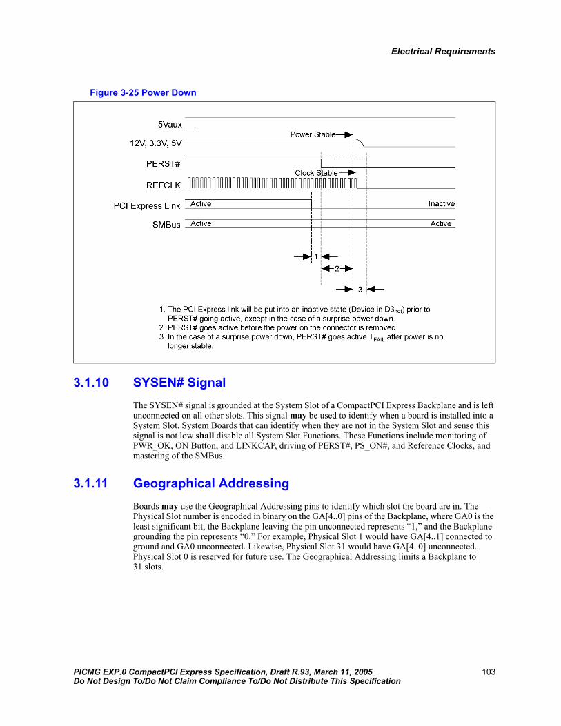
Electrical Requirements
Figure 3-25 Power Down
3.1.10 SYSEN# SignalThe SYSEN# signal is grounded at the System Slot of a CompactPCI Express Backplane and is left unconnected on all other slots. This signal may be used to identify when a board is installed into a System Slot. System Boards that can identify when they are not in the System Slot and sense this signal is not low shall disable all System Slot Functions. These Functions include monitoring of PWR_OK, ON Button, and LINKCAP, driving of PERST#, PS_ON#, and Reference Clocks, and mastering of the SMBus.
3.1.11 Geographical AddressingBoards may use the Geographical Addressing pins to identify which slot the board are in. The Physical Slot number is encoded in binary on the GA[4..0] pins of the Backplane, where GA0 is the least significant bit, the Backplane leaving the pin unconnected represents “1,” and the Backplane grounding the pin represents “0.” For example, Physical Slot 1 would have GA[4..1] connected to ground and GA0 unconnected. Likewise, Physical Slot 31 would have GA[4..0] unconnected. Physical Slot 0 is reserved for future use. The Geographical Addressing limits a Backplane to 31 slots.
PICMG EXP.0 CompactPCI Express Specification, Draft R.93, March 11, 2005 103Do Not Design To/Do Not Claim Compliance To/Do Not Distribute This Specification
Electrical Requirements
3.1.12 LINKCAP SignalThe LINKCAP signal indicates how the Backplane System Slot is routed. It can be routed assuming the System Board can operate in a 2-Link combined configuration, or only as a 4-Link configuration. To tell the System Board to configure itself for 4-Link operation, the LINKCAP pin shall be unconnected on the Backplane. To tell the System Board to operate in the combined 2-Link configuration, the LINKCAP shall be grounded on the Backplane.
A System Board shall be able to operate in the 4-Link configuration. Operating in the combined 2-Link configuration is Optional. System Boards shall disable the two unused Links when this pin is grounded. If the unused Links can be disabled only after initial Link training occurs, System Boards shall retrain the Links after disabling the unused Links and resetting any PCI Express Devices that may have been trained previously.
3.1.13 I/O PinsI/O pins may be used for Rear I/O or bussed I/O implementations. Boards and Backplanes using these pins may electrically conflict with different implementations. Refer to Section 4 for details on keying requirements to prevent installing boards in incompatible slots.
3.1.14 Reserved PinsReserved pins must be left unconnected on boards and Backplanes. They are reserved for future definition and/or for PXI.
3.2 Hot-Plug SupportThe CompactPCI Express form factor is physically different than that of a PCI card. This changes some aspects of the Hot-Plug use model but, in general, it is based on the standard model defined in the PCI Standard Hot-Plug Controller and Subsystem Specification, Revision 1.0.
This section defines additional signals required for supporting Hot-Plug of CompactPCI Express Type 1 and Type 2 Peripheral Boards. It also places additional requirements on signals previously defined in this specification when these signals are used in Hot-Plug-capable systems. This section also describes the Peripheral Board Hot-Plug features. For a detailed explanation of the register requirements and standard use model, see Section 7.7 of the PCI Express Base Specification, Revision 1.1.
3.2.1 Hot-Plug Sub-System ArchitectureThe CompactPCI Express Peripheral Board Hot-Plug model is very similar to the PCI card Hot-Plug model, with most of the same steps required. The primary differences are mechanical, along with a few electrical changes. That is, the Peripheral Board has onboard power regulation enabled after the board is installed. This changes the host adapter interface from the standard PCI and PCI Express card model. That model requires several electrical Switches to control power and interface signals on the host side of the interface, to prevent damage to the card or Host System during Hot-Plug operations.
104 PICMG EXP.0 CompactPCI Express Specification, Draft R.93, March 11, 2005Do Not Design To/Do Not Claim Compliance To/Do Not Distribute This Specification
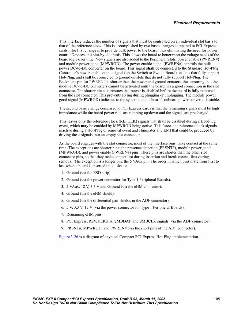
Electrical Requirements
This interface reduces the number of signals that must be controlled on an individual slot basis to that of the reference clock. This is accomplished by two basic changes compared to PCI Express cards. The first change is to provide bulk power to the board, thus eliminating the need for power control Devices on a slot-by-slot basis. This allows the board to better meet the voltage needs of the board logic over time. New signals are also added to the Peripheral Slots: power enable (PWREN#) and module power good (MPWRGD). The power enable signal (PWREN#) controls the bulk power DC-to-DC converter on the board. This signal shall be connected to the Standard Hot-Plug Controller’s power enable output signal (on the Switch or Switch Board) on slots that fully support Hot-Plug, and shall be connected to ground on slots that do not fully support Hot-Plug. The Backplane pin for PWREN# is shorter than the power and ground contacts, thus ensuring that the module DC-to-DC converters cannot be activated until the board has a good connection in the slot connector. The shorter pin also ensures that power is disabled before the board is fully removed from the slot connector. This prevents arcing during plugging or unplugging. The module power good signal (MPWRGD) indicates to the system that the board’s onboard power converter is stable.
The second basic change compared to PCI Express cards is that the remaining signals must be high impedance while the board power rails are ramping up/down and the signals are precharged.
This leaves only the reference clock (REFCLK) signals that shall be disabled during a Hot-Plug event, which may be enabled by MPWRGD being active. This forces the reference clock signals inactive during a Hot-Plug or removal event and eliminates any EMI that could be produced by driving these signals into an empty slot connector.
As the board engages with the slot connector, most of the interface pins make contact at the same time. The exceptions are shorter pins: the presence detection (PRSNT#), module power good (MPWRGD), and power enable (PWREN#) pins. These pins are shorter than the other slot connector pins, so that they make contact last during insertion and break contact first during removal. The exception is a longer pin: the 5 VAux pin. The order in which pins mate from first to last when a board is inserted into a slot is:
1. Ground (via the ESD strip).
2. Ground (via the power connector for Type 1 Peripheral Boards).
3. 5 VAux, 12 V, 3.3 V and Ground (via the eHM connector).
4. Ground (via the eHM shield).
5. Ground (via the differential pair shields in the ADF connector).
6. 5 V, 3.3 V, 12 V (via the power connector for Type 1 Peripheral Boards).
7. Remaining eHM pins.
8. PCI Express, RSV, PERST#, SMBDAT, and SMBCLK signals (via the ADF connector).
9. PRSNT#, MPWRGD, and PWREN# (via the short pins of the ADF connector).
Figure 3-26 is a diagram of a typical Compact PCI Express Hot-Plug implementation.
PICMG EXP.0 CompactPCI Express Specification, Draft R.93, March 11, 2005 105Do Not Design To/Do Not Claim Compliance To/Do Not Distribute This Specification

Electrical Requirements
Figure 3-26 Typical Hot-Plug Interface Implementation
Some of the signals in Figure 3-26 are described in the PCI Express Base Specification, Revision 1.1 and PCI Express Card Electromechanical Specification, Revision 1.1. Their minor differences are described in Table 3-26.
Table 3-26 Signals Involved in Hot-Plug
PCI Express Hot- Plug Controller
PCI Express LinkPCI Express Ref Clock
PCI Express Switch
Aux Power
PWREN#
WAKE
RST#
SMBAlert
Bulk PWR 12V, 3.3V
AUX PWR
SMBusSystem management
Bus Controller
System Management
Interface
ATN
LED
Switch Board
Peripheral Board
Host Interface
PRSNT#
PCI ExpressI/O Applications
Bulk Power converter
MPWRGD
ATNLED
PERST#
WAKE
Delay
Long Pin
Short Pin
Short Pin
Com
pact
PC
I Exp
ress
Bac
kpla
ne
ATN
SW#
ATNSW#
System Board
# #
#
Signal Name I/O Definition as Viewed From the Host Side
PWREN# O Power Enable: RequiredA slot Control Logic output that controls the slot power state. If this signal is low, power is enabled to the slot. This signal shall be grounded on slots that do not support Hot-Plug. It is point-to-point for slots that support Hot-Plug.
WAKE# I Adapter Power Request: RequiredRequests the system to return to a full power state. This signal is bussed to all slots.
MPWRGD I Module Power Good: RequiredTells the system that the bulk regulator’s outputs are up and stable. The board driver is TTL compatible for this signal and shall be pulled down by the Switch or Switch Board with a 10 KΩ ±10% resistor. The Peripheral Board shall also have a 10 KΩ ±10% resistor pull-down on the MPWRGD signal if this signal disables the precharge voltage and isolation on the WAKE# and ALERT# signals. This signal shall be left open on slots that do not support Hot-Plug. It is point-to-point for slots that support Hot-Plug.
106 PICMG EXP.0 CompactPCI Express Specification, Draft R.93, March 11, 2005Do Not Design To/Do Not Claim Compliance To/Do Not Distribute This Specification
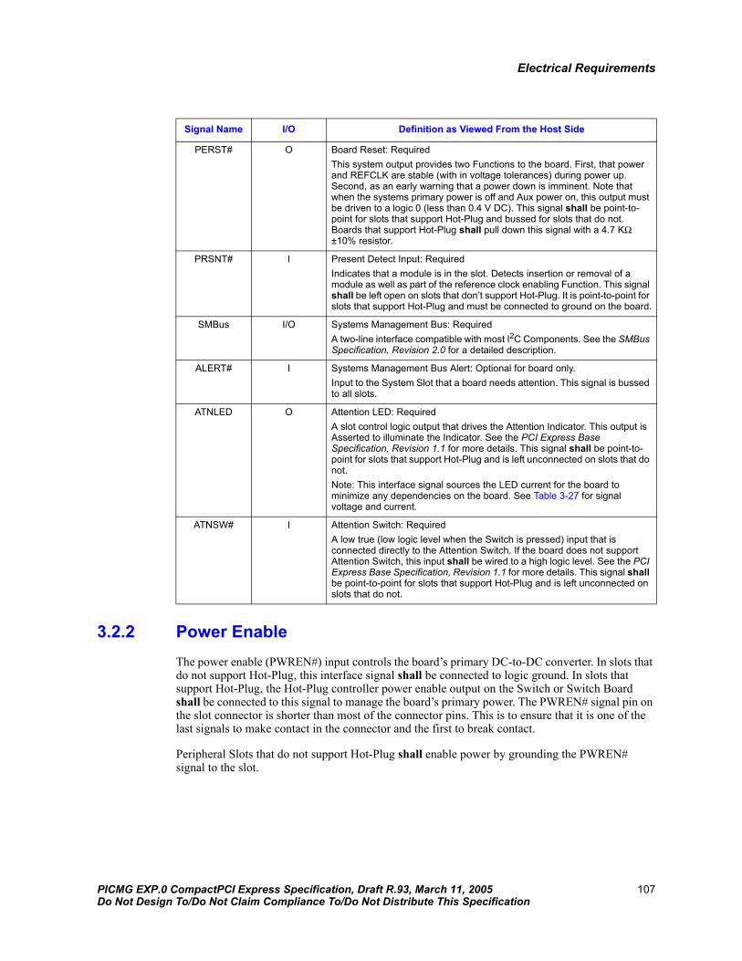
Electrical Requirements
3.2.2 Power EnableThe power enable (PWREN#) input controls the board’s primary DC-to-DC converter. In slots that do not support Hot-Plug, this interface signal shall be connected to logic ground. In slots that support Hot-Plug, the Hot-Plug controller power enable output on the Switch or Switch Board shall be connected to this signal to manage the board’s primary power. The PWREN# signal pin on the slot connector is shorter than most of the connector pins. This is to ensure that it is one of the last signals to make contact in the connector and the first to break contact.
Peripheral Slots that do not support Hot-Plug shall enable power by grounding the PWREN# signal to the slot.
PERST# O Board Reset: RequiredThis system output provides two Functions to the board. First, that power and REFCLK are stable (with in voltage tolerances) during power up. Second, as an early warning that a power down is imminent. Note that when the systems primary power is off and Aux power on, this output must be driven to a logic 0 (less than 0.4 V DC). This signal shall be point-to-point for slots that support Hot-Plug and bussed for slots that do not. Boards that support Hot-Plug shall pull down this signal with a 4.7 KΩ ±10% resistor.
PRSNT# I Present Detect Input: RequiredIndicates that a module is in the slot. Detects insertion or removal of a module as well as part of the reference clock enabling Function. This signal shall be left open on slots that don’t support Hot-Plug. It is point-to-point for slots that support Hot-Plug and must be connected to ground on the board.
SMBus I/O Systems Management Bus: RequiredA two-line interface compatible with most I2C Components. See the SMBus Specification, Revision 2.0 for a detailed description.
ALERT# I Systems Management Bus Alert: Optional for board only.Input to the System Slot that a board needs attention. This signal is bussed to all slots.
ATNLED O Attention LED: RequiredA slot control logic output that drives the Attention Indicator. This output is Asserted to illuminate the Indicator. See the PCI Express Base Specification, Revision 1.1 for more details. This signal shall be point-to-point for slots that support Hot-Plug and is left unconnected on slots that do not.Note: This interface signal sources the LED current for the board to minimize any dependencies on the board. See Table 3-27 for signal voltage and current.
ATNSW# I Attention Switch: RequiredA low true (low logic level when the Switch is pressed) input that is connected directly to the Attention Switch. If the board does not support Attention Switch, this input shall be wired to a high logic level. See the PCI Express Base Specification, Revision 1.1 for more details. This signal shall be point-to-point for slots that support Hot-Plug and is left unconnected on slots that do not.
Signal Name I/O Definition as Viewed From the Host Side
PICMG EXP.0 CompactPCI Express Specification, Draft R.93, March 11, 2005 107Do Not Design To/Do Not Claim Compliance To/Do Not Distribute This Specification

Electrical Requirements
3.2.3 Wake#The wake (WAKE#) signal is a board output that indicates that the board Requests the system to power on. See the PCI Express Base Specification, Revision 1.1 or Section 3.2 for more details on its Function.
Hot-Plug requires that WAKE# shall be properly isolated while the board is powering up and down and precharged to a voltage of 1.0 V ±20% until the board asserts MPWRGD. This prevents damage to the WAKE# circuitry and prevents the WAKE# signal from being disrupted by the Hot-Plug event.
3.2.4 Module Power GoodThe module power good (MPWRGD) signal is an active high TTL-compatible board output that indicates the onboard DC-to-DC power converters are producing stable power. The MPWRGD pin on the slot connector is shorter than most of the connector pins. This is to ensure it is one of the last signals to make contact in the connector and the first to break contact. The Hot-Plug controller and the Peripheral Board shall have a 10 KΩ ±10% pull-down on the MPWRGD signal.
3.2.5 Present DetectionThe PCI Express Hot-Plug controller detects the board presence using the presence detection signal (PRSNT#). The Root Complex or the Switch must determine the board presence and set the present bits in the appropriate register, as described in the PCI Express Base Specification, Revision 1.1. The presence detection signal shall be implemented on CompactPCI Express slots that support Hot-Plug. The presence detection signal is required on all CompactPCI Express Boards and shall be connected to ground.
The PRSNT# signal pin on the slot is shorter than most of the rest of the connector pins. This is to ensure it is one of the last signals to make contact in the connector and the first to break contact. This provides the system with valid indicator that the module is installed in the slot. See the PCI Express Base Specification, Revision 1.1 for more details on its Function.
3.2.6 System Management BusBoards that support Hot-Plug and use the SMBus shall make sure the Hot-Plug event does not affect the SMBus. This can be done using an appropriate SMBus hot-swap buffer that isolates the board from the SMBus during a Hot-Plug event and provides a precharge voltage to prevent signal disruption. See Section 3.1.1 and the PCI Express Base Specification, Revision 1.1 for more details on its Function.
3.2.7 System Management Bus AlertBoards that support Hot-Plug and use the ALERT# signal shall be properly isolated while the board is powering up and down and precharged to a voltage of 1.0 V ±20% until the board asserts MPWRGD. This prevents damage to the ALERT# circuitry and prevents the Hot-Plug event from disrupting the ALERT# signal. See Section 3.1.5 for more details on its Function.
108 PICMG EXP.0 CompactPCI Express Specification, Draft R.93, March 11, 2005Do Not Design To/Do Not Claim Compliance To/Do Not Distribute This Specification
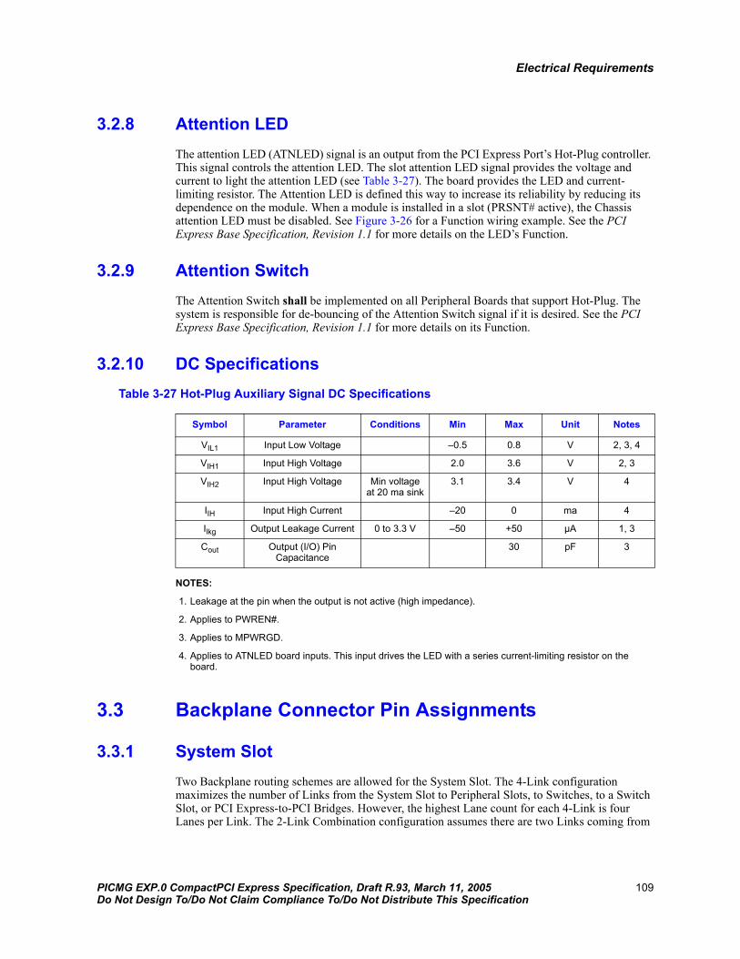
Electrical Requirements
3.2.8 Attention LEDThe attention LED (ATNLED) signal is an output from the PCI Express Port’s Hot-Plug controller. This signal controls the attention LED. The slot attention LED signal provides the voltage and current to light the attention LED (see Table 3-27). The board provides the LED and current-limiting resistor. The Attention LED is defined this way to increase its reliability by reducing its dependence on the module. When a module is installed in a slot (PRSNT# active), the Chassis attention LED must be disabled. See Figure 3-26 for a Function wiring example. See the PCI Express Base Specification, Revision 1.1 for more details on the LED’s Function.
3.2.9 Attention SwitchThe Attention Switch shall be implemented on all Peripheral Boards that support Hot-Plug. The system is responsible for de-bouncing of the Attention Switch signal if it is desired. See the PCI Express Base Specification, Revision 1.1 for more details on its Function.
3.2.10 DC SpecificationsTable 3-27 Hot-Plug Auxiliary Signal DC Specifications
NOTES:
1. Leakage at the pin when the output is not active (high impedance).
2. Applies to PWREN#.
3. Applies to MPWRGD.
4. Applies to ATNLED board inputs. This input drives the LED with a series current-limiting resistor on the board.
3.3 Backplane Connector Pin Assignments
3.3.1 System SlotTwo Backplane routing schemes are allowed for the System Slot. The 4-Link configuration maximizes the number of Links from the System Slot to Peripheral Slots, to Switches, to a Switch Slot, or PCI Express-to-PCI Bridges. However, the highest Lane count for each 4-Link is four Lanes per Link. The 2-Link Combination configuration assumes there are two Links coming from
Symbol Parameter Conditions Min Max Unit Notes
VIL1 Input Low Voltage –0.5 0.8 V 2, 3, 4
VIH1 Input High Voltage 2.0 3.6 V 2, 3
VIH2 Input High Voltage Min voltage at 20 ma sink
3.1 3.4 V 4
IIH Input High Current –20 0 ma 4
Ilkg Output Leakage Current 0 to 3.3 V –50 +50 µA 1, 3
Cout Output (I/O) Pin Capacitance
30 pF 3
PICMG EXP.0 CompactPCI Express Specification, Draft R.93, March 11, 2005 109Do Not Design To/Do Not Claim Compliance To/Do Not Distribute This Specification

Electrical Requirements
the System Board, where one of the Links can be up to eight Lanes and the other Link can be up to 16 Lanes. System Boards shall provide four Links. Some System Boards may be able to combine the four smaller Links into two larger Links, but this is not a System Board requirement.
3.3.1.1 4-Link Configuration
The 4-Link configuration of the System Slot allows the Backplane to be routed for up to four Links. The Backplane designer must determine how many of the Links are used for connection to Peripheral Slots, to Switches, or to Bridges. The Backplane designer must also determine how many Lanes are routed from each Link. Some Backplane implementations using these four Links include:
• Routing the four Links directly to four or fewer Peripheral Slots.
• Routing three of the Links directly to three or fewer Peripheral Slots and the fourth Link to a PCI Express-to-PCI Bridge to support Hybrid or Legacy Peripheral Slots.
• Routing three of the Links to Upstream Ports of Switches and the fourth Link to a PCI Express-to-PCI Bridge to support Hybrid or Legacy Peripheral Slots.
The LINKCAP pin is unconnected on the Backplane, telling the System Board to configure itself for 4-Link operation.
Figure 3-27 shows an example of Backplane routing for a 4-Link configuration system.
Figure 3-27 4-Link Configuration Backplane Example
System Slot
HybridPeripheral Slots
Legacy Peripheral Slots
x4 PCIe
x4 PCIe
x4 PCIe
x4 PCIe
PCI Bus
PCIe toPCI Bridge
110 PICMG EXP.0 CompactPCI Express Specification, Draft R.93, March 11, 2005Do Not Design To/Do Not Claim Compliance To/Do Not Distribute This Specification
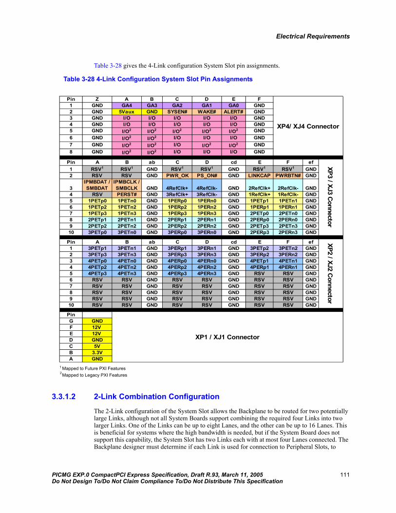
Electrical Requirements
Table 3-28 gives the 4-Link configuration System Slot pin assignments.
Table 3-28 4-Link Configuration System Slot Pin Assignments
3.3.1.2 2-Link Combination Configuration
The 2-Link configuration of the System Slot allows the Backplane to be routed for two potentially large Links, although not all System Boards support combining the required four Links into two larger Links. One of the Links can be up to eight Lanes, and the other can be up to 16 Lanes. This is beneficial for systems where the high bandwidth is needed, but if the System Board does not support this capability, the System Slot has two Links each with at most four Lanes connected. The Backplane designer must determine if each Link is used for connection to Peripheral Slots, to
Pin Z A B C D E F1 GND GA4 GA3 GA2 GA1 GA0 GND2 GND 5Vaux GND SYSEN# WAKE# ALERT# GND3 GND I/O I/O I/O I/O I/O GND4 GND I/O I/O I/O I/O I/O GND5 GND I/O2 I/O2 I/O2 I/O2 I/O2 GND6 GND I/O2 I/O2 I/O I/O I/O GND7 GND I/O2 I/O2 I/O I/O2 I/O2 GND8 GND I/O2 I/O2 I/O I/O I/O GND
Pin A B ab C D cd E F ef1 RSV1 RSV1 GND RSV1 RSV1 GND RSV1 RSV1 GND2 RSV RSV GND PWR_OK PS_ON# GND LINKCAP PWRBTN# GND
3IPMBDAT / SMBDAT
IPMBCLK / SMBCLK GND 4RefClk+ 4RefClk- GND 2RefClk+ 2RefClk- GND
4 RSV PERST# GND 3RefClk+ 3RefClk- GND 1RefClk+ 1RefClk- GND5 1PETp0 1PETn0 GND 1PERp0 1PERn0 GND 1PETp1 1PETn1 GND6 1PETp2 1PETn2 GND 1PERp2 1PERn2 GND 1PERp1 1PERn1 GND7 1PETp3 1PETn3 GND 1PERp3 1PERn3 GND 2PETp0 2PETn0 GND8 2PETp1 2PETn1 GND 2PERp1 2PERn1 GND 2PERp0 2PERn0 GND9 2PETp2 2PETn2 GND 2PERp2 2PERn2 GND 2PETp3 2PETn3 GND10 3PETp0 3PETn0 GND 3PERp0 3PERn0 GND 2PERp3 2PERn3 GND
Pin A B ab C D cd E F ef1 3PETp1 3PETn1 GND 3PERp1 3PERn1 GND 3PETp2 3PETn2 GND2 3PETp3 3PETn3 GND 3PERp3 3PERn3 GND 3PERp2 3PERn2 GND3 4PETp0 4PETn0 GND 4PERp0 4PERn0 GND 4PETp1 4PETn1 GND4 4PETp2 4PETn2 GND 4PERp2 4PERn2 GND 4PERp1 4PERn1 GND5 4PETp3 4PETn3 GND 4PERp3 4PERn3 GND RSV RSV GND6 RSV RSV GND RSV RSV GND RSV RSV GND7 RSV RSV GND RSV RSV GND RSV RSV GND8 RSV RSV GND RSV RSV GND RSV RSV GND9 RSV RSV GND RSV RSV GND RSV RSV GND10 RSV RSV GND RSV RSV GND RSV RSV GND
PinG GNDF 12V E 12V D GNDC 5VB 3.3VA GND
1 Mapped to Future PXI Features2 Mapped to Legacy PXI Features
XP4/ XJ4 Connector
XP1 / XJ1 Connector
XP3 / XJ3 Connector
XP2 / XJ2 Connector
Mapped to Future PXI FeaturesMapped to Legacy PXI Features2
1
PICMG EXP.0 CompactPCI Express Specification, Draft R.93, March 11, 2005 111Do Not Design To/Do Not Claim Compliance To/Do Not Distribute This Specification

Electrical Requirements
Switches, to Switch Slots, or to Bridges. The Backplane designer also must determine how many Lanes are routed from each Link. Some examples for Backplane implementations using these two Links include:
• Routing the two Links directly to two or fewer Peripheral Slots.
• Routing one Link directly to a Peripheral Slot and the other Link to a PCI Express-to-PCI Bridge to support Hybrid or Legacy Peripheral Slots.
• Routing the two Links to Switch Upstream Ports and using a Switch Downstream Port to connect to a PCI Express-to-PCI Bridge to support Hybrid or Legacy Peripheral Slots.
The LINKCAP pin is connected to GND on the Backplane, telling the System Board to configure itself for 2-Link operation.
Figure 3-28 shows an example of a Backplane routing for a 2-Link combination configuration system.
Figure 3-28 2-Link Combination Configuration Backplane Example
System Slot
HybridPeripheral Slots
x8 PCIe
x8 PCIe
x4 PCIex4 PCIe
x4 PCIe
x4 PCIex4 PCIe
x4 PCIe
x4 PCIe
PCI Bus Segment 1 PCI Bus Segment 2
x4 PCIe
16-lane Switch
32-lane Switch
PCIe Switch
PCIe Switch
PCIe toPCI Bridge
112 PICMG EXP.0 CompactPCI Express Specification, Draft R.93, March 11, 2005Do Not Design To/Do Not Claim Compliance To/Do Not Distribute This Specification

Electrical Requirements
Table 3-29 gives the 2-Link combination configuration System Slot pin assignments.
Table 3-29 2-Link Combination Configuration System Slot Pin Assignments
3.3.2 Peripheral Slot Type 1The Type 1 Peripheral Slot supports two use cases. The first use case is for a CPU board that can operate in either a System Slot or a Peripheral Slot through nontransparent PCI Express bridging or Advanced Switching. The second use case is for a Peripheral Board that needs the bandwidth of a x16 Link. Type 2 Peripheral Boards can physically plug in and operate in Type 1 Peripheral Slots, but the reverse is not true.
Pin Z A B C D E F1 GND GA4 GA3 GA2 GA1 GA0 GND2 GND 5Vaux GND SYSEN# WAKE# ALERT# GND3 GND I/O I/O I/O I/O I/O GND4 GND I/O I/O I/O I/O I/O GND5 GND I/O2 I/O2 I/O2 I/O2 I/O2 GND6 GND I/O2 I/O2 I/O I/O I/O GND7 GND I/O2 I/O2 I/O I/O2 I/O2 GND8 GND I/O2 I/O2 I/O I/O I/O GND
Pin A B ab C D cd E F ef1 RSV1 RSV1 GND RSV1 RSV1 GND RSV1 RSV1 GND2 RSV RSV GND PWR_OK PS_ON# GND LINKCAP PWRBTN# GND
3IPMBDAT / SMBDAT
IPMBCLK / SMBCLK GND RSVD RSVD GND RSVD RSVD GND
4 RSV PERST# GND 2RefClk+ 2RefClk- GND 1RefClk+ 1RefClk- GND5 1PETp0 1PETn0 GND 1PERp0 1PERn0 GND 1PETp1 1PETn1 GND6 1PETp2 1PETn2 GND 1PERp2 1PERn2 GND 1PERp1 1PERn1 GND7 1PETp3 1PETn3 GND 1PERp3 1PERn3 GND 1PETp4 1PETn4 GND8 1PETp5 1PETn5 GND 1PERp5 1PERn5 GND 1PERp4 1PERn4 GND9 1PETp6 1PETn6 GND 1PERp6 1PERn6 GND 1PETp7 1PETn7 GND
10 2PETp0 2PETn0 GND 2PERp0 2PERn0 GND 1PERp7 1PERn7 GND
Pin A B ab C D cd E F ef1 2PETp1 2PETn1 GND 2PERp1 2PERn1 GND 2PETp2 2PETn2 GND2 2PETp3 2PETn3 GND 2PERp3 2PERn3 GND 2PERp2 2PERn2 GND3 2PETp4 2PETn4 GND 2PERp4 2PERn4 GND 2PETp5 2PETn5 GND4 2PETp6 2PETn6 GND 2PERp6 2PERn6 GND 2PERp5 2PERn5 GND5 2PETp7 2PETn7 GND 2PERp7 2PERn7 GND 2PETp8 2PETn8 GND6 2PETp9 2PETn9 GND 2PERp9 2PERn9 GND 2PERp8 2PERn8 GND7 2PETp10 2PETn10 GND 2PERp10 2PERn10 GND 2PETp11 2PETn11 GND8 2PETp12 2PETn12 GND 2PERp12 2PERn12 GND 2PERp11 2PERn11 GND9 2PETp13 2PETn13 GND 2PERp13 2PERn13 GND 2PETp14 2PETn14 GND
10 2PETp15 2PETn15 GND 2PERp15 2PERn15 GND 2PERp14 2PERn14 GND
PinG GNDF 12V E 12V D GNDC 5VB 3.3VA GND
2 Mapped to Legacy PXI Features
XP4 / XJ4 Connector
XP3 / XJ3 Connector
XP2 / XJ2 Connector
XP1 / XJ1 Connector
1 Mapped to Future PXI FeaturesMapped to Future PXI FeaturesMapped to Legacy PXI Features
1
2
PICMG EXP.0 CompactPCI Express Specification, Draft R.93, March 11, 2005 113Do Not Design To/Do Not Claim Compliance To/Do Not Distribute This Specification

Electrical Requirements
Type 1 Peripheral Slots shall have the upper PCI Express Link in the XP3 connector routed and available for either Type 1 or Type 2 Boards to use. Type 1 Peripheral Slots may or may not have the lower PCI Express Link routed and available for Type 1 Boards.
Table 3-30 gives the Peripheral Type 1 pin assignments.
Table 3-30 Peripheral Type 1 Pin Assignments
Pin Z A B C D E F1 GND GA4 GA3 GA2 GA1 GA0 GND2 GND 5Vaux GND2 SYSEN# WAKE# ALERT# GND3 GND 12V 12V GND GND2 GND GND4 GND GND GND2 3.3V 3.3V 3.3V GND5 GND I/O2 I/O2 I/O2 I/O2 I/O2 GND6 GND I/O2 I/O2 ATNLED I/O2 I/O2 GND7 GND I/O2 I/O2 ATNSW# I/O2 I/O2 GND8 GND I/O2 I/O2 I/O I/O I/O GND
Pin A B ab C D cd E F ef1 RSV1 RSV1 GND RSV1 RSV1 GND RSV1 RSV1 GND2 PRSNT#* PWREN#* GND RSV1 RSV1 GND RSV1 RSV1 GND
3IPMBDAT / SMBDAT
IPMBCLK / SMBCLK GND RSV RSV GND RSV RSV GND
4 MPWRGD* PERST# GND 2RefClk+ 2RefClk- GND 1RefClk+ 1RefClk- GND5 1PETp0 1PETn0 GND 1PERp0 1PERn0 GND 1PETp1 1PETn1 GND6 1PETp2 1PETn2 GND 1PERp2 1PERn2 GND 1PERp1 1PERn1 GND7 1PETp3 1PETn3 GND 1PERp3 1PERn3 GND 1PETp4 1PETn4 GND8 1PETp5 1PETn5 GND 1PERp5 1PERn5 GND 1PERp4 1PERn4 GND9 1PETp6 1PETn6 GND 1PERp6 1PERn6 GND 1PETp7 1PETn7 GND
10 2PETp0 2PETn0 GND 2PERp0 2PERn0 GND 1PERp7 1PERn7 GND
Pin A B ab C D cd E F ef1 2PETp1 2PETn1 GND 2PERp1 2PERn1 GND 2PETp2 2PETn2 GND2 2PETp3 2PETn3 GND 2PERp3 2PERn3 GND 2PERp2 2PERn2 GND3 2PETp4 2PETn4 GND 2PERp4 2PERn4 GND 2PETp5 2PETn5 GND4 2PETp6 2PETn6 GND 2PERp6 2PERn6 GND 2PERp5 2PERn5 GND5 2PETp7 2PETn7 GND 2PERp7 2PERn7 GND 2PETp8 2PETn8 GND6 2PETp9 2PETn9 GND 2PERp9 2PERn9 GND 2PERp8 2PERn8 GND7 2PETp10 2PETn10 GND 2PERp10 2PERn10 GND 2PETp11 2PETn11 GND8 2PETp12 2PETn12 GND 2PERp12 2PERn12 GND 2PERp11 2PERn11 GND9 2PETp13 2PETn13 GND 2PERp13 2PERn13 GND 2PETp14 2PETn14 GND
10 2PETp15 2PETn15 GND 2PERp15 2PERn15 GND 2PERp14 2PERn14 GND
PinG GNDF 12V E 12V D GNDC 5VB 3.3VA GND
* Short Pins
2 Mapped to Legacy PXI Features
XP4 / XJ4 Connector
XP3 / XJ3 Connector
XP2 / XJ2 Connector
XP0 / XJ0 Connector
1 Mapped to Future PXI FeaturesMapped to Future PXI FeaturesMapped to Legacy PXI Features
1
2
*Short Pins
114 PICMG EXP.0 CompactPCI Express Specification, Draft R.93, March 11, 2005Do Not Design To/Do Not Claim Compliance To/Do Not Distribute This Specification

Electrical Requirements
3.3.3 Peripheral Slot Type 2The Type 2 Peripheral Slot supports Peripheral Boards that do not require higher bandwidth than a x8 Link. CPU Boards can be designed to be used as Peripheral Boards through nontransparent PCI Express bridging or Advanced Switching, but they cannot be System Boards.
Table 3-31 gives the Peripheral Slot Type 2 pin assignments.
Table 3-31 Peripheral Slot Type 2 Pin Assignments
3.3.4 Hybrid Peripheral SlotThe Hybrid Peripheral Slot supports a Type 2 Peripheral Board, a PICMG 2.0 32-bit CompactPCI Board, or a modified PXI Board. This slot type allows systems where either new CompactPCI Express Peripheral Boards or legacy Peripheral Boards can be in the same slot.
The address line to IDSEL mapping based on Logical Slot number defined in the PICMG 2.0 specification shall be used for Hybrid Peripheral Slots. The interrupt assignments based on Logical Slot number defined in the PICMG 2.0 specification shall be used for Hybrid Peripheral Slots.
Table 3-32 gives the Hybrid Peripheral Slot pin assignments.
Pin Z A B C D E F1 GND GA4 GA3 GA2 GA1 GA0 GND2 GND 5Vaux GND2 SYSEN# WAKE# ALERT# GND3 GND 12V 12V GND GND2 GND GND4 GND GND GND2 3.3V 3.3V 3.3V GND5 GND I/O2 I/O2 I/O2 I/O2 I/O2 GND6 GND I/O2 I/O2 ATNLED I/O2 I/O2 GND7 GND I/O2 I/O2 ATNSW# I/O2 I/O2 GND8 GND I/O2 I/O2 I/O I/O I/O GND
Pin A B ab C D cd E F ef1 RSV1 RSV1 GND RSV1 RSV1 GND RSV1 RSV1 GND2 PRSNT#* PWREN#* GND RSV1 RSV1 GND RSV1 RSV1 GND
3IPMBDAT / SMBDAT
IPMBCLK / SMBCLK GND RSV RSV GND RSV RSV GND
4 MPWRGD* PERST# GND RSV RSV GND 1RefClk+ 1RefClk- GND5 1PETp0 1PETn0 GND 1PERp0 1PERn0 GND 1PETp1 1PETn1 GND6 1PETp2 1PETn2 GND 1PERp2 1PERn2 GND 1PERp1 1PERn1 GND7 1PETp3 1PETn3 GND 1PERp3 1PERn3 GND 1PETp4 1PETn4 GND8 1PETp5 1PETn5 GND 1PERp5 1PERn5 GND 1PERp4 1PERn4 GND9 1PETp6 1PETn6 GND 1PERp6 1PERn6 GND 1PETp7 1PETn7 GND
10 RSV RSV GND RSV RSV GND 1PERp7 1PERn7 GND
* Short Pins
1 Mapped to Future PXI Features2 Mapped to Legacy PXI Features
XP4 / XJ4 Connector
XP3 / XJ3 Connector
Mapped to Future PXI FeaturesMapped to Legacy PXI Features
1
2
*Short Pins
PICMG EXP.0 CompactPCI Express Specification, Draft R.93, March 11, 2005 115Do Not Design To/Do Not Claim Compliance To/Do Not Distribute This Specification

Electrical Requirements
Table 3-32 Hybrid Peripheral Slot Pin Assignments
Pin Z A B C D E F1 GND GA4 GA3 GA2 GA1 GA0 GND2 GND 5Vaux GND2 SYSEN# WAKE# ALERT# GND3 GND 12V 12V GND GND2 GND GND4 GND GND GND2 3.3V 3.3V 3.3V GND5 GND I/O2 I/O2 I/O2 I/O2 I/O2 GND6 GND I/O2 I/O2 ATNLED I/O2 I/O2 GND7 GND I/O2 I/O2 ATNSW# I/O2 I/O2 GND8 GND I/O2 I/O2 I/O I/O I/O GND
Pin A B ab C D cd E F ef1 RSV1 RSV1 GND RSV1 RSV1 GND RSV1 RSV1 GND2 PRSNT#* PWREN#* GND RSV1 RSV1 GND RSV1 RSV1 GND
3IPMBDAT / SMBDAT
IPMBCLK / SMBCLK GND RSV RSV GND RSV RSV GND
4 MPWRGD* PERST# GND RSV RSV GND 1RefClk+ 1RefClk- GND5 1PETp0 1PETn0 GND 1PERp0 1PERn0 GND 1PETp1 1PETn1 GND6 1PETp2 1PETn2 GND 1PERp2 1PERn2 GND 1PERp1 1PERn1 GND7 1PETp3 1PETn3 GND 1PERp3 1PERn3 GND 1PETp4 1PETn4 GND8 1PETp5 1PETn5 GND 1PERp5 1PERn5 GND 1PERp4 1PERn4 GND9 1PETp6 1PETn6 GND 1PERp6 1PERn6 GND 1PETp7 1PETn7 GND10 RSV RSV GND RSV RSV GND 1PERp7 1PERn7 GND
Pin Z A B C D E F25 GND 5V REQ64# ENUM# 3.3V 5V GND24 GND AD[1] 5V V(I/O) AD[0] ACK64# GND23 GND 3.3V AD[4] AD[3] 5V AD[2] GND22 GND AD[7] GND 3.3V AD[6] AD[5] GND21 GND 3.3V AD[9] AD[8] M66EN C/BE[0]# GND20 GND AD[12] GND V(I/O) AD[11] AD[10] GND19 GND 3.3V AD[15] AD[14] GND AD[13] GND18 GND SERR# GND 3.3V PAR C/BE[1]# GND17 GND 3.3V IPMB_SCL IPMB_SDA GND PERR# GND16 GND DEVSEL# GND V(I/O) STOP# LOCK# GND15 GND 3.3V FRAME# IRDY# BD_SEL# TRDY# GND
12–1411 GND AD[18] AD[17] AD[16] GND C/BE[2]# GND10 GND AD[21] GND 3.3V AD[20] AD[19] GND9 GND C/BE[3]# IDSEL AD[23] GND AD[22] GND8 GND AD[26] GND V(I/O) AD[25] AD[24] GND7 GND AD[30] AD[29] AD[28] GND AD[27] GND6 GND REQ# GND 3.3V CLK AD[31] GND5 GND BRSVP1A5 BRSVP1B5 RST# GND GNT# GND4 GND IPMB_PWR HEALTHY# V(I/O) INTP INTS GND3 GND INTA# INTB# INTC# 5V INTD# GND2 GND TCK 5V TMS TDO TDI GND1 GND 5V -12V TRST# +12V 5V GND
* Short Pins
1 Mapped to Future PXI Features2 Mapped to Legacy PXI Features
P1 / J1 Connector
XP4 / XJ4 Connector
XP3 / XJ3 Connector
Key Area
Mapped to Future PXI FeaturesMapped to Legacy PXI Features
1
2
*Short Pins
116 PICMG EXP.0 CompactPCI Express Specification, Draft R.93, March 11, 2005Do Not Design To/Do Not Claim Compliance To/Do Not Distribute This Specification

Electrical Requirements
3.3.5 Legacy SlotCompactPCI Express Backplanes may include Legacy Slots that support PICMG 2.0 specification-compliant Peripheral Boards. The PICMG 2.0 specification defines pin assignments for such a slot.
The address line to IDSEL mapping based on Logical Slot number defined in the PICMG 2.0 specification shall be used for Legacy Slots. The interrupt assignments based on Logical Slot number defined in the PICMG 2.0 specification shall be used for Legacy Slots.
3.3.6 Switch SlotThe Switch Slot enables a Switch Board to distribute multiple PCIe ports across a Backplane. This specification defines the Switch Slot for both the 3U and 6U form factors, which are Optional for CompactPCI Express systems. The 3U Switch Slot pin assignments are a subset of the 6U Switch Slot. The 3U Switch Slot power connector and ADF connector spacing are mechanically identical to the 6U Switch Slot. Port assignment 1 as defined in Table 3-33 through Table 3-36 shall be used as the Upstream Port for both 3U and 6U form factors. A REFCLK shall be provided for each Port, as Table 3-33 through Table 3-36 define.
3.3.6.1 3U Switch Slot
The 3U Switch Board definition includes the XSJ1 power connector, the XSP2 ADF connector, the XSP3 ADF connector, and the XSP4 ADF connector. The Port width configuration is defined as a x4 Lane width supporting one x4 Upstream PCIe Port and up to six x4 PCIe Downstream ports. Port 1 as assigned in Table 3-33 shall be the Upstream Port. Table 3-33 defines the pinout for the 3U Switch Slot.
PICMG EXP.0 CompactPCI Express Specification, Draft R.93, March 11, 2005 117Do Not Design To/Do Not Claim Compliance To/Do Not Distribute This Specification

Electrical Requirements
Table 3-33 3U x4 Switch Slot Pin Assignments
3.3.6.2 6U Switch Slot—x4 Link Width
The 6U Switch Board definition includes the XSJ1 power connector and the XSP2 through XSP9 ADF connectors. CompactPCI Express supports two Link width configurations for 6U Switch Slots. One Link width configuration is defined as a x4 Link width, supporting one x4 Upstream PCIe ports and up to 18 PCIe Downstream ports. The other Port width configuration is defined as a
PIN A B ab C D cd E F efIPMBDAT/
SMDATIPMBCLK/
SMCLK3 7PRSNT# 7PWREN# GND 7MPWRGD 7PERST# GND 6RefClk+ 6RefClk- GND4 7RefClk+ 7RefClk- GND 7PETp0 7PETn0 GND 7PERp0 7PERn0 GND5 7PETp1 7PETn1 GND 7PETp2 7PETn2 GND 7PERp2 7PERn2 GND6 7PERp1 7PERn1 GND 7PETp3 7PETn3 GND 7PERp3 7PERn3 GND7 6ATNLED 6ATNSW# GND 6PRSNT# 6PWREN# GND 6MPWRGD 6PERST# GND8 6PETp0 6PETn0 GND 6PERp0 6PERn0 GND 6PETp1 6PETn1 GND9 6PETp2 6PETn2 GND 6PERp2 6PERn2 GND 6PERp1 6PERn1 GND10 6PETp3 6PETn3 GND 6PERp3 6PERn3 GND 5ATNLED 5ATNSW# GND
PIN A B ab C D cd E F ef1 5PRSNT# 5PWREN# GND 5MPWRGD 5PERST# GND 4RefClk+ 4RefClk- GND2 5RefClk+ 5RefClk- GND 5PETp0 5PETn0 GND 5PERp0 5PERn0 GND3 5PETp1 5PETn1 GND 5PETp2 5PETn2 GND 5PERp2 5PERn2 GND4 5PERp1 5PERn1 GND 5PETp3 5PETn3 GND 5PERp3 5PERn3 GND5 4ATNLED 4ATNSW# GND 4PRSNT# 4PWREN# GND 4MPWRGD 4PERST# GND6 4PETp0 4PETn0 GND 4PERp0 4PERn0 GND 4PETp1 4PETn1 GND7 4PETp2 4PETn2 GND 4PERp2 4PERn2 GND 4PERp1 4PERn1 GND8 4PETp3 4PETn3 GND 4PERp3 4PERn3 GND 3ATNLED 3ATNSW# GND9 3PRSNT# 3PWREN# GND 3MPWRGD 3PERST# GND 2RefClk+ 2RefClk- GND10 3RefClk+ 3RefClk- GND 3PETp0 3PETn0 GND 3PERp0 3PERn0 GND
PIN A B ab C D cd E F ef1 3PETp1 3PETn1 GND 3PETp2 3PETn2 GND 3PERp2 3PERn2 GND2 3PERp1 3PERn1 GND 3PETp3 3PETn3 GND 3PERp3 3PERn3 GND3 2ATNLED 2ATNSW# GND 2PRSNT# 2PWREN# GND 2MPWRGD 2PERST# GND4 2PETp0 2PETn0 GND 2PERp0 2PERn0 GND 2PETp1 2PETn1 GND5 2PETp2 2PETn2 GND 2PERp2 2PERn2 GND 2PERp1 2PERn1 GND6 2PETp3 2PETn3 GND 2PERp3 2PERn3 GND 1ATNLED 1ATNSW# GND7 1PRSNT# 1PWREN# GND 1MPWRGD 1PERST# GND RSV RSV GND8 1RefClk+ 1RefClk- GND 1PETp0 1PETn0 GND 1PERp0 1PERn0 GND9 1PETp1 1PETn1 GND 1PETp2 1PETn2 GND 1PERp2 1PERn2 GND10 1PERp1 1PERn1 GND 1PETp3 1PETn3 GND 1PERp3 1PERn3 GND
PIN1 12V2 GND3 GND4 3.3V5 +5V
GA0 GND
ALERT# GND 7ATNLED
GA2 GND GA11 GA4 GND GA3
XSP3 Connector
XSP2 Connector
XSJ1 Connector
2 PERST# GND 7ATNSW# GND
XSP4 Connector
WAKE#
118 PICMG EXP.0 CompactPCI Express Specification, Draft R.93, March 11, 2005Do Not Design To/Do Not Claim Compliance To/Do Not Distribute This Specification

Electrical Requirements
x8 Link width, supporting one Upstream PCIe Port and up to 8 PCIe Downstream ports. Table 3-34 and Table 3-35 define the pinout for the 6U x4-Link width Switch Slot configuration. Port 1 as assigned in Table 3-34 shall be defined as the Upstream Port.
Table 3-34 6U Switch Slot Pin Assignments for x4 Lane Configuration Part 1
PIN A B ab C D cd E F ef1 RSVD RSVD GND RSVD RSVD GND RSVD RSVD GND2 RSVD RSVD GND RSVD RSVD GND 19RefClk+ 19RefClk- GND3 19ATNLED 19ATNSW# GND 19PRSNT# 19PWREN# GND 19MPWRGD 19PERST# GND4 19PETp0 19PETn0 GND 19PERp0 19PERn0 GND 19PETp1 19PETn1 GND5 19PETp2 19PETn2 GND 19PERp2 19PERn2 GND 19PERp1 19PERn1 GND6 19PETp3 19PETn3 GND 19PERp3 19PERn3 GND 18ATNLED 18ATNSW# GND7 18PRSNT# 18PWREN# GND 18MPWRGD 18PERST# GND 17RefClk+ 17RefClk- GND8 18RefClk+ 18RefClk- GND 18PETp0 18PETn0 GND 18PERp0 18PERn0 GND9 18PETp1 18PETn1 GND 18PETp2 18PETn2 GND 18PERp2 18PERn2 GND10 18PERp1 18PERn1 GND 18PETp3 18PETn3 GND 18PERp3 18PERn3 GND
PIN A B ab C D cd E F ef1 17ATNLED 17ATNSW# GND 17PRSNT# 17PWREN# GND 17MPWRGD 17PERST# GND2 17PETp0 17PETn0 GND 17PERp0 17PERn0 GND 17PETp1 17PETn1 GND3 17PETp2 17PETn2 GND 17PERp2 17PERn2 GND 17PERp1 17PERn1 GND4 17PETp3 17PETn3 GND 17PERp3 17PERn3 GND 16ATNLED 16ATNSW# GND5 16PRSNT# 16PWREN# GND 16MPWRGD 16PERST# GND 15RefClk+ 15RefClk- GND6 16RefClk+ 16RefClk- GND 16PETp0 16PETn0 GND 16PERp0 16PERn0 GND7 16PETp1 16PETn1 GND 16PETp2 16PETn2 GND 16PERp2 16PERn2 GND8 16PERp1 16PERn1 GND 16PETp3 16PETn3 GND 16PERp3 16PERn3 GND9 15ATNLED 15ATNSW# GND 15PRSNT# 15PWREN# GND 15MPWRGD 15PERST# GND10 15PETp0 15PETn0 GND 15PERp0 15PERn0 GND 15PETp1 15PETn1 GND
PIN A B ab C D cd E F ef1 15PETp2 15PETn2 GND 15PERp2 15PERn2 GND 15PERp1 15PERn1 GND2 15PETp3 15PETn3 GND 15PERp3 15PERn3 GND 14ATNLED 14ATNSW# GND3 14PRSNT# 14PWREN# GND 14MPWRGD 14PERST# GND 13RefClk+ 13RefClk- GND4 14RefClk+ 14RefClk- GND 14PETp0 14PETn0 GND 14PERp0 14PERn0 GND5 14PETp1 14PETn1 GND 14PETp2 14PETn2 GND 14PERp2 14PERn2 GND6 14PERp1 14PERn1 GND 14PETp3 14PETn3 GND 14PERp3 14PERn3 GND7 13ATNLED 13ATNSW# GND 13PRSNT# 13PWREN# GND 13MPWRGD 13PERST# GND8 13PETp0 13PETn0 GND 13PERp0 13PERn0 GND 13PETp1 13PETn1 GND9 13PETp2 13PETn2 GND 13PERp2 13PERn2 GND 13PERp1 13PERn1 GND10 13PETp3 13PETn3 GND 13PERp3 13PERn3 GND 12ATNLED 12ATNSW# GND
PIN A B ab C D cd E F ef1 12PRSNT# 12PWREN# GND 12MPWRGD 12PERST# GND 11RefClk+ 11RefClk- GND2 12RefClk+ 12RefClk- GND 12PETp0 12PETn0 GND 12PERp0 12PERn0 GND3 12PETp1 12PETn1 GND 12PETp2 12PETn2 GND 12PERp2 12PERn2 GND4 12PERp1 12PERn1 GND 12PETp3 12PETn3 GND 12PERp3 12PERn3 GND5 11ATNLED 11ATNSW# GND 11PRSNT# 11PWREN# GND 11MPWRGD 11PERST# GND6 11PETp0 11PETn0 GND 11PERp0 11PERn0 GND 11PETp1 11PETn1 GND7 11PETp2 11PETn2 GND 11PERp2 11PERn2 GND 11PERp1 11PERn1 GND8 11PETp3 11PETn3 GND 11PERp3 11PERn3 GND 10ATNLED 10ATNSW# GND9 10PRSNT# 10PWREN# GND 10MPWRGD 10PERST# GND 9RefClk+ 9RefClk- GND10 10RefClk+ 10RefClk- GND 10PETp0 10PETn0 GND 10PERp0 10PERn0 GND
XSP6 Connector
XSP9 Connector
XSP8 Connector
XSP7 Connector
PICMG EXP.0 CompactPCI Express Specification, Draft R.93, March 11, 2005 119Do Not Design To/Do Not Claim Compliance To/Do Not Distribute This Specification

Electrical Requirements
Table 3-35 6U Switch Slot Pin Assignments for x4 Lane Configuration Part 2
PIN A B ab C D cd E F ef1 10PETp1 10PETn1 GND 10PETp2 10PETn2 GND 10PERp2 10PERn2 GND2 10PERp1 10PERn1 GND 10PETp3 10PETn3 GND 10PERp3 10PERn3 GND3 9ATNLED 9ATNSW# GND 9PRSNT# 9PWREN# GND 9MPWRGD 9PERST# GND4 9PETp0 9PETn0 GND 9PERp0 9PERn0 GND 9PETp1 9PETn1 GND5 9PETp2 9PETn2 GND 9PERp2 9PERn2 GND 9PERp1 9PERn1 GND6 9PETp3 9PETn3 GND 9PERp3 9PERn3 GND 8ATNLED 8ATNSW# GND7 8PRSNT# 8PWREN# GND 8PERST# GND RSV RSV GND8 8RefClk+ 8RefClk- GND 8PETp0 8PETn0 GND 8PERp0 8PERn0 GND9 8PETp1 8PETn1 GND 8PETp2 8PETn2 GND 8PERp2 8PERn2 GND10 8PERp1 8PERn1 GND 8PETp3 8PETn3 GND 8PERp3 8PERn3 GND
PIN A B ab C D cd E F efIPMBDAT/
SMDATIPMBCLK/
SMCLK3 7PRSNT# 7PWREN# GND 7MPWRGD 7PERST# GND 6RefClk+ 6RefClk- GND4 7RefClk+ 7RefClk- GND 7PETp0 7PETn0 GND 7PERp0 7PERn0 GND5 7PETp1 7PETn1 GND 7PETp2 7PETn2 GND 7PERp2 7PERn2 GND6 7PERp1 7PERn1 GND 7PETp3 7PETn3 GND 7PERp3 7PERn3 GND7 6ATNLED 6ATNSW# GND 6PRSNT# 6PWREN# GND 6MPWRGD 6PERST# GND8 6PETp0 6PETn0 GND 6PERp0 6PERn0 GND 6PETp1 6PETn1 GND9 6PETp2 6PETn2 GND 6PERp2 6PERn2 GND 6PERp1 6PERn1 GND10 6PETp3 6PETn3 GND 6PERp3 6PERn3 GND 5ATNLED 5ATNSW# GND
PIN A B ab C D cd E F ef1 5PRSNT# 5PWREN# GND 5MPWRGD 5PERST# GND 4RefClk+ 4RefClk- GND2 5RefClk+ 5RefClk- GND 5PETp0 5PETn0 GND 5PERp0 5PERn0 GND3 5PETp1 5PETn1 GND 5PETp2 5PETn2 GND 5PERp2 5PERn2 GND4 5PERp1 5PERn1 GND 5PETp3 5PETn3 GND 5PERp3 5PERn3 GND5 4ATNLED 4ATNSW# GND 4PRSNT# 4PWREN# GND 4MPWRGD 4PERST# GND6 4PETp0 4PETn0 GND 4PERp0 4PERn0 GND 4PETp1 4PETn1 GND7 4PETp2 4PETn2 GND 4PERp2 4PERn2 GND 4PERp1 4PERn1 GND8 4PETp3 4PETn3 GND 4PERp3 4PERn3 GND 3ATNLED 3ATNSW# GND9 3PRSNT# 3PWREN# GND 3MPWRGD# 3PERST# GND 2RefClk+ 2RefClk- GND10 3RefClk+ 3RefClk- GND 3PETp0 3PETn0 GND 3PERp0 3PERn0 GND
PIN A B ab C D cd E F ef1 3PETp1 3PETn1 GND 3PETp2 3PETn2 GND 3PERp2 3PERn2 GND2 3PERp1 3PERn1 GND 3PETp3 3PETn3 GND 3PERp3 3PERn3 GND3 2ATNLED 2ATNSW# GND 2PRSNT# 2PWREN# GND 2MPWRGD 2PERST# GND4 2PETp0 2PETn0 GND 2PERp0 2PERn0 GND 2PETp1 2PETn1 GND5 2PETp2 2PETn2 GND 2PERp2 2PERn2 GND 2PERp1 2PERn1 GND6 2PETp3 2PETn3 GND 2PERp3 2PERn3 GND 1ATNLED 1ATNSW# GND7 1PRSNT# 1PWREN# GND 1MPWRGD 1PERST# GND RSV RSV GND8 1RefClk+ 1RefClk- GND 1PETp0 1PETn0 GND 1PERp0 1PERn0 GND9 1PETp1 1PETn1 GND 1PETp2 1PETn2 GND 1PERp2 1PERn2 GND10 1PERp1 1PERn1 GND 1PETp3 1PETn3 GND 1PERp3 1PERn3 GND
PIN1 12V
2 GND
3 GND
4 3.3V
5 +5V
1 GA4 GND
GND 7ATNLED
GA3 GA2 GND GA1
2 PERST# GND WAKE#
XSJ1 Connector
XSP5 Connector
XSP4 Connector
XSP3 Connector
XSP2 Connector
7ATNSW# GND
GA0 GND
ALERT#
120 PICMG EXP.0 CompactPCI Express Specification, Draft R.93, March 11, 2005Do Not Design To/Do Not Claim Compliance To/Do Not Distribute This Specification

Electrical Requirements
3.3.6.3 6U Switch Slot—x8 Link Width
Table 3-36 and Table 3-37 define the pinout for the 6U x8 Link width Switch Slot configuration. Port 1 as assigned in Table 3-36 shall be defined as the Upstream Port.
Table 3-36 6U Switch Slot Pin Assignments for x8 Lane Configuration Part 1
PIN A B ab C D cd E F ef1 RSVD RSVD GND RSVD RSVD GND RSVD RSVD GND2 RSVD RSVD GND RSVD RSVD GND 9RefClk+ 9RefClk- GND3 9ATNLED 9ATNSW# GND 9PRSNT# 9PWREN# GND 9MPWRGD 9PERST# GND4 9PETp0 9PETn0 GND 9PERp0 9PERn0 GND 9PETp1 9PETn1 GND5 9PETp2 9PETn2 GND 9PERp2 9PERn2 GND 9PERp1 9PERn1 GND6 9PETp3 9PETn3 GND 9PERp3 9PERn3 GND RSVD RSVD GND7 RSVD RSVD GND RSVD RSVD GND 8RefClk+ 8RefClk- GND8 RSVD RSVD GND 9PETp4 9PETn4 GND 9PERp4 9PERn4 GND9 9PETp5 9PETn5 GND 9PETp6 9PETn6 GND 9PERp6 9PERn6 GND10 9PERp5 9PERn5 GND 9PETp7 9PETn7 GND 9PERp7 9PERn7 GND
PIN A B ab C D cd E F ef1 8ATNLED 8ATNSW# GND 8PRSNT# 8PWREN# GND 8MPWRGD 8PERST# GND2 8PETp0 8PETn0 GND 8PERp0 8PERn0 GND 8PETp1 8PETn1 GND3 8PETp2 8PETn2 GND 8PERp2 8PERn2 GND 8PERp1 8PERn1 GND4 8PETp3 8PETn3 GND 8PERp3 8PERn3 GND RSVD RSVD GND5 RSVD RSVD GND RSVD RSVD GND 7RefClk+ 7RefClk- GND6 RSVD RSVD GND 8PETp4 8PETn4 GND 8PERp4 8PERn4 GND7 8PETp5 8PETn5 GND 8PETp6 8PETn6 GND 8PERp6 8PERn6 GND8 8PERp5 8PERn5 GND 8PETp7 8PETn7 GND 8PERp7 8PERn7 GND9 7ATNLED 7ATNSW# GND 7PRSNT# 7PWREN# GND 7MPWRGD 7PERST# GND10 7PETp0 7PETn0 GND 7PERp0 7PERn0 GND 7PETp1 7PETn1 GND
PIN A B ab C D cd E F ef1 7PETp2 7PETn2 GND 7PERp2 7PERn2 GND 7PERp1 7PERn1 GND2 7PETp3 7PETn3 GND 7PERp3 7PERn3 GND RSVD RSVD GND3 RSVD RSVD GND RSVD RSVD GND 6RefClk+ 6RefClk- GND4 RSVD RSVD GND 7PETp4 7PETn4 GND 7PERp4 7PERn4 GND5 7PETp5 7PETn5 GND 7PETp6 7PETn6 GND 7PERp6 7PERn6 GND6 7PERp5 7PERn5 GND 7PETp7 7PETn7 GND 7PERp7 7PERn7 GND7 6ATNLED 6ATNSW# GND 6PRSNT# 6PWREN# GND 6MPWRGD 6PERST# GND8 6PETp0 6PETn0 GND 6PERp0 6PERn0 GND 6PETp1 6PETn1 GND9 6PETp2 6PETn2 GND 6PERp2 6PERn2 GND 6PERp1 6PERn1 GND10 6PETp3 6PETn3 GND 6PERp3 6PERn3 GND RSVD RSVD GND
PIN A B ab C D cd E F ef1 RSVD RSVD GND RSVD RSVD GND 5RefClk+ 5RefClk- GND2 RSVD RSVD GND 6PETp4 6PETn4 GND 6PERp4 6PERn4 GND3 6PETp5 6PETn5 GND 6PETp6 6PETn6 GND 6PERp6 6PERn6 GND4 6PERp5 6PERn5 GND 6PETp7 6PETn7 GND 6PERp7 6PERn7 GND5 5ATNLED 5ATNSW# GND 5PRSNT# 5PWREN# GND 5MPWRGD 5PERST# GND6 5PETp0 5PETn0 GND 5PERp0 5PERn0 GND 5PETp1 5PETn1 GND7 5PETp2 5PETn2 GND 5PERp2 5PERn2 GND 5PERp1 5PERn1 GND8 5PETp3 5PETn3 GND 5PERp3 5PERn3 GND RSVD RSVD GND9 RSVD RSVD GND RSVD RSVD GND 4RefClk+ 4RefClk- GND10 RSVD RSVD GND 5PETp4 5PETn4 GND 5PERp4 5PERn4 GND
XSP9 Connector
XSP7 Connector
XSP6 Connector
XSP8 Connector
PICMG EXP.0 CompactPCI Express Specification, Draft R.93, March 11, 2005 121Do Not Design To/Do Not Claim Compliance To/Do Not Distribute This Specification

Electrical Requirements
Table 3-37 6U Switch Slot Pin Assignments for x8 Lane Configuration Part 2
PIN A B ab C D cd E F ef1 5PETp5 5PETn5 GND 5PETp6 5PETn6 GND 5PERp6 5PERn6 GND2 5PERp5 5PERn5 GND 5PETp7 5PETn7 GND 5PERp7 5PERn7 GND3 4ATNLED 4ATNSW# GND 4PRSNT# 4PWREN# GND 4MPWRGD 4PERST# GND4 4PETp0 4PETn0 GND 4PERp0 4PERn0 GND 4PETp1 4PETn1 GND5 4PETp2 4PETn2 GND 4PERp2 4PERn2 GND 4PERp1 4PERn1 GND6 4PETp3 4PETn3 GND 4PERp3 4PERn3 GND RSVD RSVD GND7 RSVD RSVD GND RSVD RSVD GND RSV RSV GND8 RSVD RSVD GND 4PETp4 4PETn4 GND 4PERp4 4PERn4 GND9 4PETp5 4PETn5 GND 4PETp6 4PETn6 GND 4PERp6 4PERn6 GND10 4PERp5 4PERn5 GND 4PETp7 4PETn7 GND 4PERp7 4PERn7 GND
PIN A B ab C D cd E F efIPMBDAT/
SMDATIPMBCLK/
SMCLK3 RVSD RVSD GND RVSD RVSD GND 3RefClk+ 3RefClk- GND4 RVSD RVSD GND RVSD RVSD GND RVSD RVSD GND5 RVSD RVSD GND RVSD RVSD GND RVSD RVSD GND6 RVSD RVSD GND RVSD RVSD GND RVSD RVSD GND7 3ATNLED 3ATNSW# GND 3PRSNT# 3PWREN# GND 3MPWRGD 3PERST# GND8 3PETp0 3PETn0 GND 3PERp0 3PERn0 GND 3PETp1 3PETn1 GND9 3PETp2 3PETn2 GND 3PERp2 3PERn2 GND 3PERp1 3PERn1 GND10 3PETp3 3PETn3 GND 3PERp3 3PERn3 GND RSVD RSVD GND
PIN A B ab C D cd E F ef1 RSVD RSVD GND RSVD RSVD GND 2RefClk+ 4RefClk- GND2 RSVD RSVD GND 3PETp4 3PETn4 GND 3PERp4 3PERn4 GND3 3PETp5 3PETn5 GND 3PETp6 3PETn6 GND 3PERp6 3PERn6 GND4 3PERp5 3PERn5 GND 3PETp7 3PETn7 GND 3PERp7 3PERn7 GND5 2ATNLED 2ATNSW# GND 2PRSNT# 2PWREN# GND 2MPWRGD 2PERST# GND6 2PETp0 2PETn0 GND 2PERp0 2PERn0 GND 2PETp1 2PETn1 GND7 2PETp2 2PETn2 GND 2PERp2 2PERn2 GND 2PERp1 2PERn1 GND8 2PETp3 2PETn3 GND 2PERp3 2PERn3 GND RSVD RSVD GND9 RSVD RSVD GND RSVD RSVD GND 1RefClk+ 1RefClk- GND10 RSVD RSVD GND 2PETp4 2PETn4 GND 2PERp4 2PERn4 GND
PIN A B ab C D cd E F ef1 2PETp5 2PETn5 GND 2PETp6 2PETn6 GND 2PERp6 2PERn6 GND2 2PERp5 2PERn5 GND 2PETp7 2PETn7 GND 2PERp7 2PERn7 GND3 1ATNLED 1ATNSW# GND 1PRSNT# 2PWREN# GND 1MPWRGD 1PERST# GND4 1PETp0 1PETn0 GND 1PERp0 2PERn0 GND 1PETp1 1PETn1 GND5 1PETp2 1PETn2 GND 1PERp2 2PERn2 GND 1PERp1 1PERn1 GND6 1PETp3 1PETn3 GND 1PERp3 2PERn3 GND RSVD RSVD GND7 RSVD RSVD GND RSVD RSVD GND RSVD RSVD GND8 RSVD RSVD GND 1PETp4 1PETn4 GND 1PERp4 1PERn4 GND9 1PETp5 1PETn5 GND 1PETp6 1PETn6 GND 1PERp6 1PERn6 GND10 1PERp5 1PERn5 GND 1PETp7 1PETn7 GND 1PERp7 1PERn7 GND
PIN1 12V
2 GND
3 GND
4 3.3V
5 +5V
RVSD GND
GA0 GND
GND RVSD2 PERST# GND
1 GA4 GND GA3
XSJ1 Connector
XSP5 Connector
XSP4 C
onnectorXSP3 C
onnectorXSP2 C
onnector
GA2 GND GA1
WAKE# ALERT#
122 PICMG EXP.0 CompactPCI Express Specification, Draft R.93, March 11, 2005Do Not Design To/Do Not Claim Compliance To/Do Not Distribute This Specification

Electrical Requirements
3.4 Power Supply RequirementsThis specification defines the power rails for powering boards of 12 V, 3.3 V, 5 V, and 5 Vaux. All four power rails are available on System Slots and Type 1 Peripheral Slots. Type 2 Peripheral Slots and the portion of the Hybrid Peripheral Slot that supports Type 2 Peripherals do not have access to 5 V. Refer to PICMG 2.0 (CompactPCI) for power supply and decoupling requirements for Legacy Slots and for the P1 connector of Hybrid Peripheral Slot.
–12 V shall be available for Hybrid and Legacy Peripheral Slots. See PICMG 2.0 (CompactPCI) for –12 V specifications.
CompactPCI Express Backplanes and systems may support the use of modular CompactPCI pluggable power supplies defined in the PICMG 2.11 specification, provided the use of such a supply does not violate any requirements of this specification.
3.4.1 Current AvailableCompactPCI Express systems shall provide all rails defined for a given slot type, but the amount of current available on each rail is not defined. Table 3-38 lists the maximum current for each slot type based on the type and number of pins.
Table 3-38 Maximum Current Available Through Pins
Slot Type 12 V 3.3 V 5 V 5 Vaux -12 V Notes
System Slot 30 A 15 A 15 A 1 A N/A Max combined current from 12 V, 3.3 V, and 5 V is 45 A.
Peripheral Slot Type 1
32 A 18 A 15 A 1 A N/A Max combined current from 12 V, 3.3 V, and 5 V is 50 A.
Peripheral Slot Type 2
2 A 3 A N/A 1 A N/A
Hybrid Peripheral
Slot
2 A 3 A See Note
1 A See Note
Refer to the CompactPCI specification for current available on P1 connector.
Legacy Slot See Note
See Note
See Note
See Note
See Note
Refer to the CompactPCI specification for current available on P1 and P2 connector.
PICMG EXP.0 CompactPCI Express Specification, Draft R.93, March 11, 2005 123Do Not Design To/Do Not Claim Compliance To/Do Not Distribute This Specification

Electrical Requirements
3.4.2 Regulation and Ripple and NoiseTable 3-39 Regulation and Ripple and Noise
3.4.3 Backplane Power DecouplingTable 3-40 lists the minimum power decoupling that shall be implemented for every slot of a CompactPCI Backplane by slot type. The capacitors for power decoupling on the Backplane shall have a voltage rating of at least three times the voltage of the rail where the capacitor is used, except for the +12 V and –12 V rails. The capacitors for power decoupling on the Backplane for the +12 V and –12 V rails shall have a voltage rating of at least 35 V. The capacitance tolerance of the capacitors for power decoupling on the Backplane shall be ±20% or better. The capacitors should be placed as close as possible to the connectors and voltage pins being decoupled.
Table 3-40 Minimum Power Decoupling Requirements
3.4.4 Power Supply TimingThe 12 V and 5 V output levels must be equal to or greater than the 3.3 V output at all times during power-up and normal operation.
Voltage RegulationMax Ripple and Noise (pk-pk)
20 MHz Bandwidth Limit
Notes
12 V ±5% 120 mV Refer to the CompactPCI specification when providing power to P1 of Hybrid Peripheral Slots or Legacy Slots.
5 V ±5% 50 mV Refer to the CompactPCI specification when providing power to P1 of Hybrid Peripheral Slots or Legacy Slots.
3.3 V ±5% 50 mV Refer to the CompactPCI specification when providing power to P1 of Hybrid Peripheral Slots or Legacy Slots.
5 Vaux ±5% 50 mV Refer to the CompactPCI specification when providing power to P1 of Hybrid Peripheral Slots or Legacy Slots.
–12 V See Note See Note Refer to the CompactPCI specification when providing power to P1 of Hybrid Peripheral Slots or Legacy Slots.
Slot Type 3.3 V 5 V 5 Vaux V(I/O) +12 V –12 V
System 44 uF 44 uF 0 N/A 44 uF N/A
Type 1 44 uF 44 uF 0 N/A 44 uF N/A
Type 2 44 uF N/A 0 N/A 44 uF N/A
Hybrid 88 uF 44 uF 0 44uF 59 uF 15 uF
Switch 44 uF 44 uF N/A N/A 44 uF N/A
Legacy 44 uF 44 uF 0 44uF 15 uF 15 uF
124 PICMG EXP.0 CompactPCI Express Specification, Draft R.93, March 11, 2005Do Not Design To/Do Not Claim Compliance To/Do Not Distribute This Specification

Electrical Requirements
The power-on time is defined as the time from when PS_ON# is pulled low to when the 12 V, 5 V, and 3.3 V outputs are within the regulation ranges Section 3.4.2 specifies. The power-on time shall be less than 500 ms (T1 < 500 ms, see Figure 3-20).
5 Vaux shall have a power-on time of 2 seconds maximum after application of valid AC voltages.
The output voltages shall rise from 10% of nominal to within the regulation ranges specified in Table 3-39 within 0.1 ms to 20 ms (0.1 ms ≤ T2 ≤ 20 ms, see Figure 3-20).
3.4.5 Additional Power Requirements for Boards Supporting Hot-PlugBoards that support Hot-Plug shall meet the requirements listed in Table 3-41.
Table 3-41 Board Hot-Plug Capacitance and Current Limits
NOTES:
1. Max Initial Hot-Plug Capacitance includes the drain-source and drain-gate capacitance of the MOSFET (COSS) Switch that isolates the board backend supply from the input.
2. Max Board Capacitance is calculated assuming the capacitance charges up in 5 ms, with current slewing at the maximum allowed rate, up to the maximum allowed current. Maximum allowed current is 32 A for 12 V, 15 A for 5 V, and 18 A for 3.3 V (see Table 3-13).
3. Max Initial Hot-Plug Capacitance applies to the 5 VAux rail only if a MOSFET Switch (and not a resistor) isolates input from the board circuits powering off that rail.
4. Max Board Capacitance for the 5 VAux rail is calculated assuming a total available time of 3 ms for pre-charge. The pre-charge resistor would be 3.3 V/220 mA = 15, and 3 x 15 x 68 uF = 3 ms.
Power Rail Max Current Slew Rate
Max Initial Hot-Plug
Capacitance (1)Peak Precharge
CurrentMax Board
Capacitance
12 V 3 A/ms 10 nF N/A 3000 uF (2)
5 V 3 A/ms 10 nF N/A 7500 uF (2)
3.3 V 3 A/ms 10 nF N/A 11,000 uF (2)
5 VAux 0.3 A/ms 10 nF (3) 220 mA 68 uF (4)
PICMG EXP.0 CompactPCI Express Specification, Draft R.93, March 11, 2005 125Do Not Design To/Do Not Claim Compliance To/Do Not Distribute This Specification

Keying Requirements
Keying Requirements 4
This section covers the keying requirements for CompactPCI Express Boards, Backplanes, and Chassis.
4.1 Legacy Slots and Legacy BoardsLegacy Slot and Legacy Board keying shall meet the PICMG 2.10 Revision 1.0 specification (Keying of CompactPCI Boards and Backplanes) requirements.
4.2 eHM KeyingThe eHM connector was designed to have four keying positions that protect against electrically incompatible uses of the connector I/O pins. The different uses of the eHM I/O pins for boards and slots include the following:
• I/O pins not used.
• I/O pins used for Rear I/O.
• I/O pins used for extended Rear I/O on a System Board and System Slot. Extended Rear I/O on a System Board and System Slot is where pins are used in column 3 or column 4 for Rear I/O. If such a System Board is plugged into a Type 1 Peripheral Slot, there may be an electrical conflict with the power and ground pins defined in column 3 and 4 of the Type 1 Peripheral Slot.
• I/O pins used for PXI.
• I/O pins used for bussed interconnect.
Table 4-1 shows the compatibility between these different board and slot types. The compatibility between a slot that supports Rear I/O and the different board types assumes no rear transition module is populated. If a module is populated, there may be an incompatibility between the board and rear transition module that the table does not account for.
126 PICMG EXP.0 CompactPCI Express Specification, Draft R.93, March 11, 2005Do Not Design To/Do Not Claim Compliance To/Do Not Distribute This Specification

Keying Requirements
Table 4-1 Electrical Compatibility Between eHM I/O Pin Uses
Table 4-2 shows the different eHM male connector keying designators and the associated keying assignments based on a slot’s eHM I/O pin use. Table 4-3 shows the different eHM female connector keying designators and the associated keying assignments based on a board’s eHM I/O pin use.
Table 4-2 eHM Male Connector Keying Designators
Table 4-3 eHM Female Connector Keying Designators
Matching colors between the Table 4-2 and Table 4-3 indicate a board and slot are prevented from mating due to incompatibility.
CompactPCI Express Type 1 Peripheral Slots, Type 2 Peripheral Slots, Hybrid Peripheral Slots, and System Slots shall use the eHM connector type listed in Table 4-2 based on the use of eHM I/O pin use indicated in that table.
Slot eHM I/O Pin Use
Rear I/O or Not Used
(Peripheral Slot)
Read I/O or Not Used
(System Slot)
Extended Rear I/O in
System Slot
PXI Bussed Interconnect
Boa
rd e
HM
I/O
Pin
Use Rear I/O OK OK Conflict Conflict Conflict
Extended Rear I/O on System Board
Conflict OK OK Conflict Conflict
PXI OK OK Conflict OK Conflict
Bussed Interconnect OK OK Conflict Conflict OK
Not Used OK OK Conflict OK OK
Male Keying Designator Slot eHM I/O Pin Use Key Pos 1 Key Pos 2 Key Pos 3 Key Pos 4
1 Rear I/O or Not Used (Peripheral Slot) Fill Empty Empty Empty
2 PXI Fill Empty Fill Empty
3 Bussed Interconnect Fill Fill Empty Empty
4 Extended Rear I/O in System Slot Empty Empty Empty Fill
5 Rear I/O or Not Used (System Slot) Empty Empty Empty Empty
Female Keying Designator Board eHM I/O Pin Use Key Pos 1 Key Pos 2 Key Pos 3 Key Pos 4
1 Rear I/O Empty Fill Fill Fill
2 PXI Empty Fill Empty Fill
3 Bussed Interconnect Empty Empty Fill Fill
4 Extended Rear I/O on System Board Fill Empty Empty Empty
5 Not Used Empty Empty Empty Fill
PICMG EXP.0 CompactPCI Express Specification, Draft R.93, March 11, 2005 127Do Not Design To/Do Not Claim Compliance To/Do Not Distribute This Specification

Keying Requirements
CompactPCI Express Type 1 Peripheral Boards, Type 2 Peripheral Boards, and System Boards shall use the eHM connector type listed in Table 4-3 based on the use of eHM I/O pin use indicated in that table.
Additional RI/O or Bussed I/O keying for the eHM connector shall be implemented through front panel keys specified in the PICMG 2.10 Revision 1.0 specification (Keying of CompactPCI Boards and Backplanes). This shall be done based on the J2 front panel key allocation in the PICMG 2.10 specification, although J2 is not used on boards with eHM connectors.
128 PICMG EXP.0 CompactPCI Express Specification, Draft R.93, March 11, 2005Do Not Design To/Do Not Claim Compliance To/Do Not Distribute This Specification

CompactPCI Express Advanced Differential Fabric Connector
CompactPCI Express Advanced Differential Fabric Connector A
A.1 General DataIn accordance with PICMG Policies and Procedures, Tyco Electronics Corp., ERNI, and Broadside Technologies Inc. have jointly committed to grant licenses under reasonable and nondiscriminatory terms to the intellectual property of those companies necessary to manufacture the Advanced Differential Fabric connector (ADF) for PICMG applications. Neither Tyco, ERNI, nor Broadside Technologies warrants that the license conveyed is sufficient to manufacture the connector without infringing the intellectual property rights of third parties.
A.1.1 Objective of this Document The objective of this document is to provide information for designing and manufacturing the Advance Differential Fabric connector (ADF) for PICMG applications. The information presented is public domain information and does not knowingly infringe the intellectual property rights of third parties.
A.1.2 ScopeThis section provides information regarding the design requirements for compatible application and mechanical end electrical performance requirements. This section is meant to be a general design guide for product intermatability and performance. The approach is to define the true position of the contacts and blades in the Header, the aperture in the Front Board connector, the mating condition, the PCB layout patterns, and the electrical performance requirements. The design of a compliant connector and the additional information required are the manufacturer’s responsibility. Because some characteristics of the connector system are dependent on design, a given Front Board should be assembled with connectors of only one design. The same advice should also be followed for populating a single slot in a Backplane. This ensures the most performance uniformity. The electrical requirements set forth in Section 3 and the mechanical requirements set forth in Section 2 serve as the overall requirements for functionality. This section sets forth environmental requirements. If additional information is required, it is the connector manufacturer’s responsibility and may be determined by agreement between the manufacturer and user.
A.1.3 Intended Method of MountingThese connectors are designed for pressfit assembly. The Front Board connector is designed for flat rock assembly, and the Backplane connector requires a special press tool.
PICMG EXP.0 CompactPCI Express Specification, Draft R.93, March 11, 2005 129Do Not Design To/Do Not Claim Compliance To/Do Not Distribute This Specification

CompactPCI Express Advanced Differential Fabric Connector
A.1.4 Ratings and CharacteristicsThe standard connector offering is for pressfit assembly, with IEC Performance Level 2 contacts capable of 250 mating cycles as per IEC 60512-5, Test 9a, under the test conditions specified in paragraph 4.3.1, Mechanical Operation, in IEC 61076-4-101. The connectors are also available with other plating specifications to meet specific requirements such as Telecordia GR-1217 large systems and uncontrolled environments or Mil C-55110.
A.1.5 Normative ReferencesUL 60950 UL Standard for Safety for Information Technology Equipment. December 2, 2000.
CSA C22.2 No. 182.4-M90, Plugs, Receptacles, and Connectors for Communication Systems—Wiring Products.
Telecordia GR-1217 CORE, Level I, Central Office or Uncontrolled Environment.
IEC 60068-1:1998, Environmental testing. Part 1 General and guidance.
IEC 60068-2-60:1990, Corrosion tests in artificial atmosphere at very low concentration of polluting gasses.
IEC 60352-1 1993, Solderless Connections. Part 5—Solderless press-in connections—General requirements, test methods, and practical guidance.
IEC 60512-1:1984, Electromechanical components for electronic equipment; basic testing procedures and tests, insulation tests, and voltage stress tests.
IEC 60512-2:1985, Electromechanical components for electronic equipment; basic testing procedures and measuring methods. Part 2—General examination, electrical continuity, and contact resistance tests and voltage stress tests.
IEC 60512-3:1976, Electromechanical components for electronic equipment; basic testing procedures and measuring methods. Part 3—Current carrying capacity tests.
IEC 60512-4:1976, Electromechanical components for electronic equipment; basic testing procedures and measuring methods. Part 4—Dynamic stress tests.
IEC 60512-5:1992, Electromechanical components for electronic equipment; basic testing procedures and measuring methods. Part 5—Impact tests (free components), static load tests (fixed components), endurance tests, and overload tests.
IEC 60512-6:1984, Electromechanical components for electronic equipment; basic testing procedures and measuring methods. Part 6—Climatic tests and soldering tests.
IEC 60512-7:1992, Electromechanical components for electronic equipment; basic testing procedures and measuring methods. Part 7—Mechanical operating tests and sealing tests.
IEC 60512-8:1985, Electromechanical components for electronic equipment; basic testing procedures and measuring methods. Part 8—Connector tests (mechanical) and mechanical tests on contacts and terminations. Amendment 1.
130 PICMG EXP.0 CompactPCI Express Specification, Draft R.93, March 11, 2005Do Not Design To/Do Not Claim Compliance To/Do Not Distribute This Specification

CompactPCI Express Advanced Differential Fabric Connector
IEC 60512-9:1976, Electromechanical components for electronic equipment; basic testing procedures and measuring methods. Part 9 Cable clamping tests, explosion hazard tests, chemical resistance tests, fire hazard tests, r.f. resistance tests, capacitance tests, shielding and filtering tests, and magnetic interference tests.
IEC 60512-11-7:1976, Flowing mixed gas corrosion test.
ISO 468:1982, Surface roughness—Parameters, their values, and general rules for specifying requirements.
IEC 60352-2: Solderless connections—Part 2: Solderless crimped connections. General requirements, test methods, and practical guidance.
IEC 60352-3: Solderless connections—Part 3: Solderless accessible insulation displacement connections. General requirements, test methods, and practical guidance.
IEC 60352-5: Solderless connections—Part 5: Press-in connections. General requirements, test.
IEC 61076-1: 1995, Generic Specification: Connectors with assessed quality, for use in d.c. and low-frequency analogue applications and in digital applications employing high-speed data rates.
IEC 61076-3: Connectors with assessed quality, for use in d.c., low-frequency analog, and digital high-speed data applications. Part 3: Rectangular connectors. Proposed.
IEC 61076-4: 1995, Sectional Specification: Connectors with assessed quality, for use in d.c. and low-frequency analogue applications and in digital applications employing high-speed data rates, for use with printed boards. Methods and practical guidance (second edition).
IEC Guide 109: 1995, Environmental aspects—Inclusion in electrotechnical product standards.
A.1.6 MarkingsThe “A” row is marked in the plastic body of the Backplane connector, and column 1 is also marked. On the Front Board connector, row and column nomenclature are not required.
A.1.7 Type DesignationConnectors to which this connector specification apply may be designated by the following part numbers as defined in Section A.1.8 and special loadings as defined in Section 1.9.
Front Board connector type designation: ADF-F-3-10-2-F-25
Backplane connector type designation: ADF-M-3-10-2-B-25
Backplane connector XP7 type designation: ADF-M-3-10-2-S-25-0100
Backplane connector XP3 type designation: ADF-M-3-10-2-S-25-0100
PICMG EXP.0 CompactPCI Express Specification, Draft R.93, March 11, 2005 131Do Not Design To/Do Not Claim Compliance To/Do Not Distribute This Specification

CompactPCI Express Advanced Differential Fabric Connector
A.1.8 Ordering InformationFigure A-1 Sample Part Number with Explanation
A.1.9 Special Connector LoadingsBackplane connectors specified for the XP7 and XP3 positions for certain slots have special loadings in accordance with Figure A-2 and shall be designated as loading configuration 0100.
ADF
Connector Designation
Contact Type(M = Pin, F = Receptacle)
Number of Rows (Pairs)(2, 3, 4, 5)
Number of Columns (Wafers)(03, 05, 10, 15, 17, 19, 20)
Plating Class(1 = I, 2 = II, 3 = III)
Signal Contact Length (Above Backplane)(A = 6.8, B = 8.3, F = Receptacle, S = Special Custom Staging)
Terminal Lengths(22 = 2.2 mm (Receptacle Only), 18 = 1.8 mm, 25 = 2.5 mm, 37 = 3.7 mm (Male Only))
Special Contact Loading(Only if Specified by "S")
Bold characters indicate standard selection for CompactPCI Express applications.
132 PICMG EXP.0 CompactPCI Express Specification, Draft R.93, March 11, 2005Do Not Design To/Do Not Claim Compliance To/Do Not Distribute This Specification

CompactPCI Express Advanced Differential Fabric Connector
Figure A-2 Special Connector Loading 0100
A.2 Technical Information
A.2.1 Contacts and TerminationsOn the Backplane connector, the pressfit terminals are offered in various lengths. The specific style and dimensions of terminations may be determined by agreement between the connector manufacturer and user. The contacts are plated to IEC Performance Level 2 (250 mating cycles).
On the Front Board connector, the press fit terminals are 2.2 mm. The specific style and dimensions of terminations may be determined by agreement between the connector manufacturer and user. The contacts are plated to IEC Performance Level 2 (250 mating cycles).
1
2
3
4
56
7
89
10
1
2
3
4
56
7
89
10
a b ab c d cd e f ef
Gro
und
Gro
und
Gro
und
a b ab c d cd e f ef
Gro
und
Gro
und
Gro
und
Standard Contact Loading 0100 Contact Loading
8.3 mm Signal Contact
6.8 mm Signal Contact 9.35 mm Ground "L" Blade
PICMG EXP.0 CompactPCI Express Specification, Draft R.93, March 11, 2005 133Do Not Design To/Do Not Claim Compliance To/Do Not Distribute This Specification
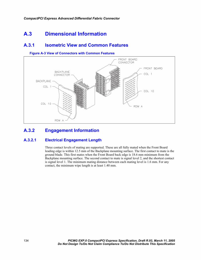
CompactPCI Express Advanced Differential Fabric Connector
A.3 Dimensional Information
A.3.1 Isometric View and Common FeaturesFigure A-3 View of Connectors with Common Features
A.3.2 Engagement Information
A.3.2.1 Electrical Engagement Length
Three contact levels of mating are supported. These are all fully mated when the Front Board leading edge is within 12.5 mm of the Backplane mounting surface. The first contact to mate is the ground blade. This first mates when the Front Board back edge is 18.6 mm minimum from the Backplane mounting surface. The second contact to mate is signal level 2, and the shortest contact is signal level 1. The minimum mating distance between each mating level is 1.6 mm. For any contact, the minimum wipe length is at least 1.40 mm.
134 PICMG EXP.0 CompactPCI Express Specification, Draft R.93, March 11, 2005Do Not Design To/Do Not Claim Compliance To/Do Not Distribute This Specification
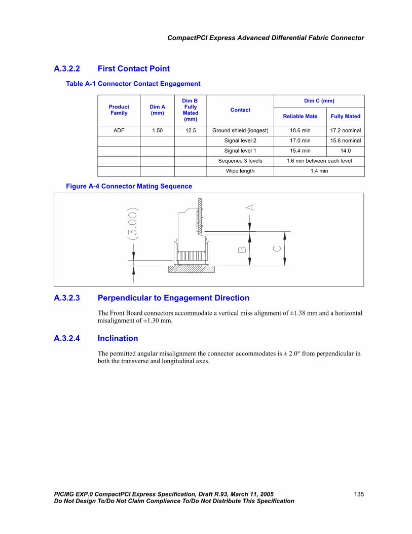
CompactPCI Express Advanced Differential Fabric Connector
A.3.2.2 First Contact Point
Table A-1 Connector Contact Engagement
Figure A-4 Connector Mating Sequence
A.3.2.3 Perpendicular to Engagement Direction
The Front Board connectors accommodate a vertical miss alignment of ±1.38 mm and a horizontal misalignment of ±1.30 mm.
A.3.2.4 Inclination
The permitted angular misalignment the connector accommodates is ± 2.0° from perpendicular in both the transverse and longitudinal axes.
Product Family
Dim A(mm)
Dim B Fully
Mated(mm)
ContactDim C (mm)
Reliable Mate Fully Mated
ADF 1.50 12.5 Ground shield (longest) 18.6 min 17.2 nominal
Signal level 2 17.0 min 15.6 nominal
Signal level 1 15.4 min 14.0
Sequence 3 levels 1.6 min between each level
Wipe length 1.4 min
PICMG EXP.0 CompactPCI Express Specification, Draft R.93, March 11, 2005 135Do Not Design To/Do Not Claim Compliance To/Do Not Distribute This Specification

CompactPCI Express Advanced Differential Fabric Connector
A.3.3 Backplane Connectors
A.3.3.1 Dimensions
Figure A-5 Dimensional Drawing of Backplane Connector
A.3.3.2 Contacts
The ground blade contact length is 6.3 mm ±0.5 mm. The signal level 2 contact nominal length is 5.3 mm, and the signal level 1 nominal length is 5.3 mm.
136 PICMG EXP.0 CompactPCI Express Specification, Draft R.93, March 11, 2005Do Not Design To/Do Not Claim Compliance To/Do Not Distribute This Specification

CompactPCI Express Advanced Differential Fabric Connector
A.3.3.3 Contact Tip Geometry
Figure A-6 Contact Geometry for Zone 2 Backplane Connector
A.3.3.4 Terminations
The contact terminal lengths are by agreement between the connector suppliers and their customers. The current standard pressfit terminal length for the Backplane Header is 2.5 mm ref.
H 0.25 M
M
M
0.06 H
0.2
Rounded
0.4 0–0.04
0.5 0–0.01 0.25
M0.06
0.4
0–0
.01
0.16 max 0.25 max
M0.10
0.6
max
0.6
max
G
–0.2 0
PICMG EXP.0 CompactPCI Express Specification, Draft R.93, March 11, 2005 137Do Not Design To/Do Not Claim Compliance To/Do Not Distribute This Specification

CompactPCI Express Advanced Differential Fabric Connector
A.3.4 Front Board Connectors
A.3.4.1 Dimensions
Figure A-7 Dimensional Drawing of Front Board Connectors
A.3.4.2 Terminations
The current standard pressfit terminal length for the Front Board connectors is 2.2 mm ref.
A.3.5 Mounting Information for Backplane ConnectorsThe ADF connector requires a 0.55–0.65 mm plated via. The centerline of row “b” on the Backplane connector aligns with the Front Board Component Side 1.
138 PICMG EXP.0 CompactPCI Express Specification, Draft R.93, March 11, 2005Do Not Design To/Do Not Claim Compliance To/Do Not Distribute This Specification
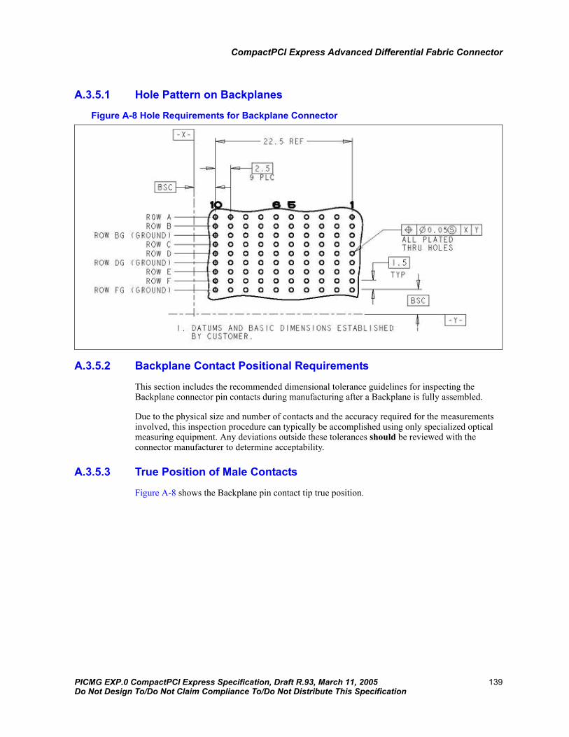
CompactPCI Express Advanced Differential Fabric Connector
A.3.5.1 Hole Pattern on Backplanes
Figure A-8 Hole Requirements for Backplane Connector
A.3.5.2 Backplane Contact Positional Requirements
This section includes the recommended dimensional tolerance guidelines for inspecting the Backplane connector pin contacts during manufacturing after a Backplane is fully assembled.
Due to the physical size and number of contacts and the accuracy required for the measurements involved, this inspection procedure can typically be accomplished using only specialized optical measuring equipment. Any deviations outside these tolerances should be reviewed with the connector manufacturer to determine acceptability.
A.3.5.3 True Position of Male Contacts
Figure A-8 shows the Backplane pin contact tip true position.
PICMG EXP.0 CompactPCI Express Specification, Draft R.93, March 11, 2005 139Do Not Design To/Do Not Claim Compliance To/Do Not Distribute This Specification

CompactPCI Express Advanced Differential Fabric Connector
Figure A-9 Backplane Pin Contact Positional Tolerance
A.3.6 Mounting Information for Front Board Connectors
A.3.6.1 Hole Pattern on Printed Boards
Figure A-10 Hole Requirements for the Front Board Connector
140 PICMG EXP.0 CompactPCI Express Specification, Draft R.93, March 11, 2005Do Not Design To/Do Not Claim Compliance To/Do Not Distribute This Specification

CompactPCI Express Advanced Differential Fabric Connector
A.4 CharacteristicsConnectors must meet the performance requirements outlined in the following subsections.
A.4.1 Climatic CategoryTests shall be performed at ambient environmental conditions as per IEC-60512 Electrical.
A.4.1.1 Climatic Category Test batch P: Initial Examination
Table A-2 Test Batch P
A.4.1.2 Climatic Category Test Batch A: Mechanical Tests
Table A-3 Test Batch A
Test Phase
Test Measurement to be Performed Requirements
TitleIEC
60512 Test
Severity or Condition of
TestTitle
IEC 60512 Test
PL
P1 General information
1a, 1b Unmated connectors
Visual examination
1a 2 x There shall be no defect that would impair normal operation.
Dimensional examination
1b 2 x Creepage and Clearance 0.3 mm minimum.
P2 Polarizing method
13e Force to be applied: 62.5 N
Physical handling
2 x It shall be possible to correctly align and mate the connectors. It shall not be possible to mate the connectors incorrectly.
P3 Contact resistance
2a Millivolt method
Contact resistance
2a 2 x Signal: _ 50 mΩ
P4 Insulation resistance
3a Test voltage100 V
± 15 V DCMethod B
Insulation resistance
3a 2 x Signal + shield: _ to 1010 Ω
P5 Voltage proof 4a Method B 500 V eff
Voltage proof 4aMethod B
2 x No flashover between signals and grounds
Test Phase
Test Measurement to be Performed Requirements
TitleIEC
60512 Test
Severity or Condition of Test Title IEC 60512
Test PL
A1.1 Insertion and
withdrawal forces
13a _ 40 N Mate and Unmate Forces
13a 2 x
PICMG EXP.0 CompactPCI Express Specification, Draft R.93, March 11, 2005 141Do Not Design To/Do Not Claim Compliance To/Do Not Distribute This Specification
CompactPCI Express Advanced Differential Fabric Connector
A5 Contact retention in
insert
15a Test forceinsertion direction:
44.5 N max.withdrawal direction:
4.4 N min.
Contact retention in
insert
15a 2 x
A7 Vibration 6d 2e 10 Hz–2000 Hz acceleration
1.5 mm or 200 m/s2
number of cycles: 8Duration: 3 x 2h
Contact disturbance
2e 2 x Contact disturbance: 1 µs
Visual examination
1a Visual examination
1a 2 x No damage likely to impair normal operation.
A8 Contact resistance
2a Millivolt method for signal and shield
contacts
Contact resistance
2a 2 x (After test reqs.)Signal: ∆ ≤ 10 mΩShield: ∆ ≤ 10 mΩ
Shock 6c 2e Shock acceleration 500 ms2
Duration: 11 msNumber of cycles: 5
Contact disturbance
2e 2 x Contact disturbance: 1 µs
Visual examination
1a Visual examination
1a 2 x No damage likely to impair normal operation.
Contact resistance
2a Millivolt method for signal and shield
contacts
Contact resistance
2a 2 x (After test reqs.)Signal: ∆ ≤ 10 mΩShield: ∆ ≤ 10 mΩ
A10 Rapid change of
temperature
11d -50°C to 105°C mated
Connectors duration: 30 min
Number of cycles: 5
2 x Observe preparation
Insulation resistance
3a Test voltage100 V ± 15 V DC
Method B
Insulation resistance
3a 2 x Signal + shield: ≥ 1010 Ω
Voltage proof
4a Method B500 V eff
Voltage proof
4aMethod B
2 x No flashover
Visual examination
1a Visual examination
1A 2 x No damage likely to impair normal operation.
A11.1 Dry heat 11i + 105°CDuration: 16 h
Test voltage: 100 V 15 V DCMethod B
Insulation resistance
at high tempera-
tures
3a 2 x Requirements, see Clause A.4.2.5.Signal + shield: ≥ 1010 Ω
A11.2 Damp heat, cyclic, first
cycle
11mMethod
1
+ 55°CRecovery time: 2h
Visual examination
1a 2 x No damage likely to impair normal operation.
A11.3 Cold 11j - 55°CDuration: 2h
Recovery time: 2h
Visual examination
1a 2 x No damage likely to impair normal operation.
142 PICMG EXP.0 CompactPCI Express Specification, Draft R.93, March 11, 2005Do Not Design To/Do Not Claim Compliance To/Do Not Distribute This Specification

CompactPCI Express Advanced Differential Fabric Connector
A11.5 Damp heat, cyclic,
remaining cycles
11m + 55°CRecovery time: 2h
Insulation resistance
3a Test voltage100 V ± 15 V DC
Method B
Insulation resistance
3a 2 x Signal + shield: ≥ 1010 Ω
Contact resistance
2a Millivolt method for signal and shield
contacts
Contact resistance
2a 2 x (After test reqs.)Signal: ∆ ≤ 10 mΩShield: ∆ ≤ 10 mΩ
Voltage proof
4a Method B500 V eff
Voltage proof
4aMethod B
2 x No flashover
A12.1 Insertion and
withdrawal forces
13b Mate and Unmate Forces
13b 2 x Requirements, see Clause A.4.3.2≤ 40 N
A13 Visual examination
Unmated Visual examination
1a 2 x No damage likely to impair normal operation.
PICMG EXP.0 CompactPCI Express Specification, Draft R.93, March 11, 2005 143Do Not Design To/Do Not Claim Compliance To/Do Not Distribute This Specification

CompactPCI Express Advanced Differential Fabric Connector
A.4.1.3 Climatic Category Test Batch B: Harsh Environments
Table A-4 Test Batch B
Test Phase
Test Measurement to be Performed Requirements
TitleIEC
60512 Test
Severity or Condition of
TestTitle
IEC 60512 Test
PL
B2 Mechanical operations
9a Speed max. 10 mm/s
Rest period 30 s unmated
2 x 125 cycles
Visual examination
1a Unmated connectors
Visual examination
1a 2 x No damage likely to impair normal operation.
Contact resistance
2a Millivolt method for signal and
shield contacts
Contact resistance
2a 2 x (After test reqs.)Signal: ∆ ≤ 10 mΩShield: ∆ ≤ 10 mΩ
Insulation resistance
3a Test voltage100 V
± 15 V DCMethod B
Insulation resistance
3a 2 x Signal + shield: ≥ 1010 Ω
Voltage proof 4a Method B500 V eff
Voltage proof
4aMethod B
2 x No flashover
B3.2 Corrosion, Industrial
atmosphere
11g + 25° C/75% relative humidityGas concentration: mixed gas 0.5 PPM SO2 + 0.1 PPM H2SDuration: 4 days
Contact resistance
2a Millivolt method for signal and
shield contacts
Contact resistance
2a 2 x (After test reqs.)Signal: ∆ ≤ 10 mΩShield: ∆ ≤ 10 mΩ
144 PICMG EXP.0 CompactPCI Express Specification, Draft R.93, March 11, 2005Do Not Design To/Do Not Claim Compliance To/Do Not Distribute This Specification

CompactPCI Express Advanced Differential Fabric Connector
B4 Mechanical operations
9a Speed max. 10 mm/s
Rest period 30s unmated
2 x 125 cycles
Visual examination
1a Unmated connectors
Visual examination
2 x No damage likely to impair normal operation.
Contact resistance
2a Millivolt method for signal and
shield contacts
Contact resistance
2a 2 x (After test reqs.)Signal: ∆ ≤ 10 mΩShield: ∆ ≤ 10 mΩ
Insulation resistance
3a Test voltage100 V
± 15 V DCMethod B
Insulation resistance
3a 2 x Signal + shield: ≥ 1010 Ω
Voltage proof 4a Method B500 V eff
Voltage proof
4aMethod B
2 x No flashover
Gauge retention force
16e Gauge retention
force
16e 2 x Signal + shield: ≥ 0.1 N
B6 Static load 8a Applied forces:F1 = 50 N, F2 =
40 N,F3 = 25 N
2 x After removal of applied forces, there shall be no displacement of the connector on the PCB that could impair normal operation.
Visual examination
Unmated connectors
Visual examination
1a 2 x No damage likely to impair normal operation.
PICMG EXP.0 CompactPCI Express Specification, Draft R.93, March 11, 2005 145Do Not Design To/Do Not Claim Compliance To/Do Not Distribute This Specification

CompactPCI Express Advanced Differential Fabric Connector
A.4.1.4 Climatic Category Test Batch C: Damp Heat
Table A-5 Test Batch C
Test Phase
Test Measurement to be Performed Requirements
Title IEC 60512 Test no.
Severity or Condition of test Title
IEC 60512
Test no.PL
C1 Damp heat, Steady heat
11c + 40°C93% rel. humidity
Aging time: 21 days
Preparation
Insulation resistance
3a Test voltage100 V ± 15 V DC
Method B
Insulation resistance
3a 2 x Signal + shield: ≥ 1010 Ω
Contact resistance
2a Millivolt method for signal and
shield contacts
Contact resistance
2a 2 x (After test reqs.)Signal: ∆ ≤ 10 mΩShield: ∆ ≤ 10 mΩ
Voltage proof
4a Method B500 V eff
Voltage proof 4aMethod
B
2 x No flashover
Insertion and
withdrawal forces
13a Insertion and withdrawal
forces
13a 2 x ≤ 40 N
Visual examination
1a Unmated connectors
Visual examination
1a 2 x No damage likely to impair normal operation.
146 PICMG EXP.0 CompactPCI Express Specification, Draft R.93, March 11, 2005Do Not Design To/Do Not Claim Compliance To/Do Not Distribute This Specification
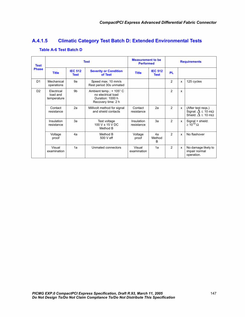
CompactPCI Express Advanced Differential Fabric Connector
A.4.1.5 Climatic Category Test Batch D: Extended Environmental Tests
Table A-6 Test Batch D
Test Phase
Test Measurement to be Performed Requirements
Title IEC 512 Test
Severity or Condition of Test Title IEC 512
Test PL
D1 Mechanical operations
9a Speed max. 10 mm/sRest period 30s unmated
2 x 125 cycles
D2 Electrical load and
temperature
9b Ambient temp.: + 105° C no electrical loadDuration: 1000 h
Recovery time: 2 h
2 x
Contact resistance
2a Millivolt method for signal and shield contacts
Contact resistance
2a 2 x (After test reqs.)Signal: ∆ ≤ 10 mΩShield: ∆ ≤ 10 mΩ
Insulation resistance
3a Test voltage100 V ± 15 V DC
Method B
Insulation resistance
3a 2 x Signal + shield: ≥ 1010 Ω
Voltage proof
4a Method B500 V eff
Voltage proof
4a Method
B
2 x No flashover
Visual examination
1a Unmated connectors Visual examination
1a 2 x No damage likely to impair normal operation.
PICMG EXP.0 CompactPCI Express Specification, Draft R.93, March 11, 2005 147Do Not Design To/Do Not Claim Compliance To/Do Not Distribute This Specification

CompactPCI Express Advanced Differential Fabric Connector
A.4.1.6 Climatic Category Test Batch E: Extended Environmental Tests
Table A-7 Test Batch E
A.4.2 Electrical CharacteristicsTable A-8 Electrical Characteristics
A.4.2.1 Impedance
50 ps Edge Rate (20–80%) 100 Ω ±10%
100 ps Edge Rate (20–80%) 100 Ω ±10%
Test Phase
Test Measurement to be Performed Requirements
TitleIEC
60512 Test
Severity or Condition of Test Title
IEC 60512 Test
PL
E1 Robustness of terminations
16f Test force: 50 N
Unmated connectors Visual examination
1a 2 x No damage likely to impair normal operation.
E2 Contact retention
15a Test force:Insertion direction: 4 N
Withdrawal direction: 10 N
Contact retention
15a 2 x Max. displacement allowed after removal of test force: 0.1 mm
Visual examination
1a Unmated connectors Visual examination
1a 2 x No damage likely to impair normal
operation.
E4 Mould growth 11e C. of C. Certificate of compliance of
connector material is available.
E5 Flammability 20a Flame exposure time: 10 s 2 x Post burning time max.: 10 s
Characteristic and Condition Requirement Test
Impedance EIA 364-108
50 ps Edge Rate (20–80%) 100 Ω ±10%
100 ps Edge Rate (20–80%) 100 Ω ±10%
Crosstalk Noise EIA 364-90
NEN—Worst-Case Multiaggressor < 3% @ 100 ps
FEN—Worst-Case Multiaggressor < 3% @ 100 ps
Propagation Delay (w/footprint*) EIA 364-103
Insertion Loss < 1 dB @ 3 GHz EIA 364-101
148 PICMG EXP.0 CompactPCI Express Specification, Draft R.93, March 11, 2005Do Not Design To/Do Not Claim Compliance To/Do Not Distribute This Specification

CompactPCI Express Advanced Differential Fabric Connector
A.4.2.2 Crosstalk
Near End Noise—Worst-Case Multiaggressor < 3% @ 100 ps
Far End Noise—Worst-Case Multiaggressor < 3% @ 100 ps
A.4.2.3 Propagation Delay
Table A-9 Propagation Delay
A.4.2.4 Differential Skew
Table A-10 Differential Skew
A.4.2.5 Insertion Loss
< 1 dB @ 3 GHz
Propagation Delay (w/Footprint*) EIA 364-103
A Pin 107 ±13 ps
B Pin 117 ±13 ps
C Pin 135 ±13 ps
D Pin 144 ±13 ps
E Pin 167 ±13 ps
F Pin 176 ±13 ps
Differential Pair Maximum Skew
Propagation pin B minus propagation pin A 11 ±2 ps
Propagation pin D minus propagation pin C 11 ±2 ps
Propagation pin F minus propagation pin E 11 ±2 ps
PICMG EXP.0 CompactPCI Express Specification, Draft R.93, March 11, 2005 149Do Not Design To/Do Not Claim Compliance To/Do Not Distribute This Specification
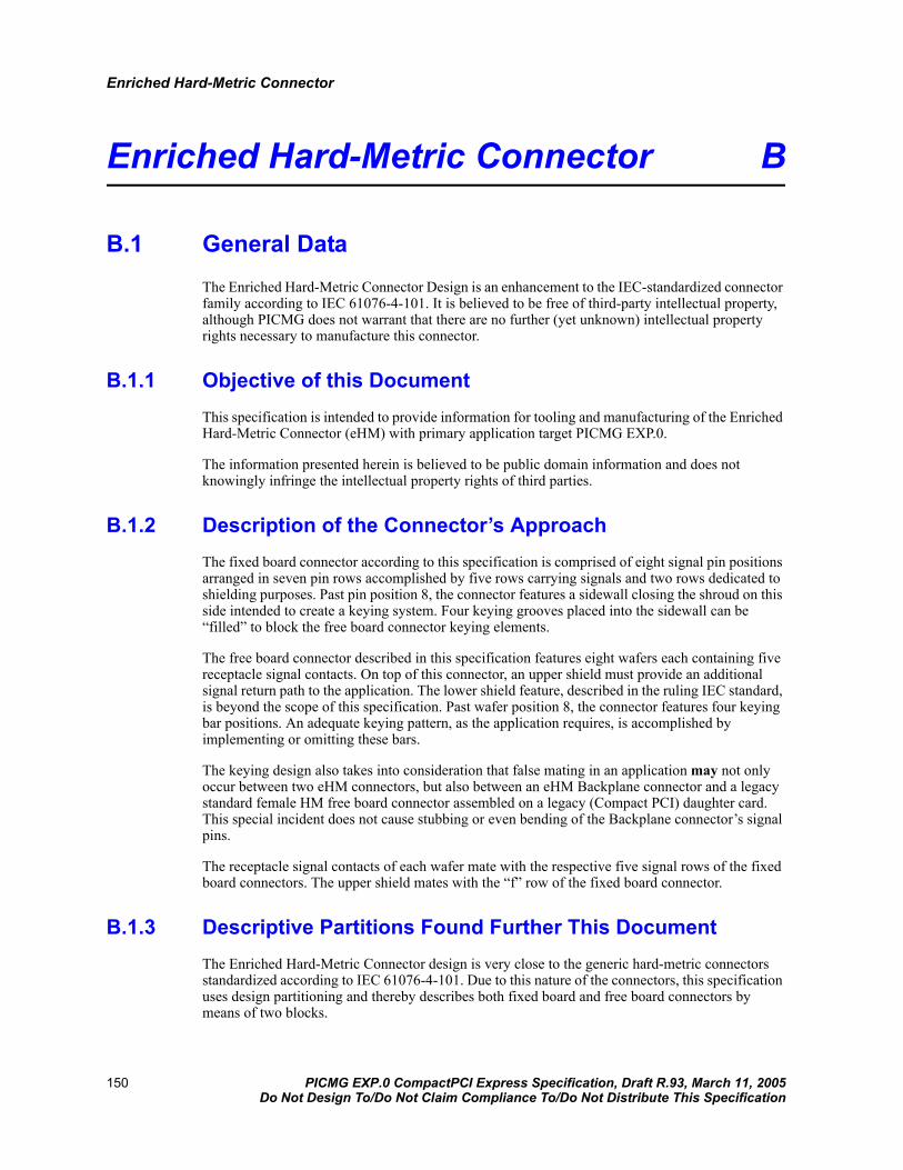
Enriched Hard-Metric Connector
Enriched Hard-Metric Connector B
B.1 General DataThe Enriched Hard-Metric Connector Design is an enhancement to the IEC-standardized connector family according to IEC 61076-4-101. It is believed to be free of third-party intellectual property, although PICMG does not warrant that there are no further (yet unknown) intellectual property rights necessary to manufacture this connector.
B.1.1 Objective of this DocumentThis specification is intended to provide information for tooling and manufacturing of the Enriched Hard-Metric Connector (eHM) with primary application target PICMG EXP.0.
The information presented herein is believed to be public domain information and does not knowingly infringe the intellectual property rights of third parties.
B.1.2 Description of the Connector’s ApproachThe fixed board connector according to this specification is comprised of eight signal pin positions arranged in seven pin rows accomplished by five rows carrying signals and two rows dedicated to shielding purposes. Past pin position 8, the connector features a sidewall closing the shroud on this side intended to create a keying system. Four keying grooves placed into the sidewall can be “filled” to block the free board connector keying elements.
The free board connector described in this specification features eight wafers each containing five receptacle signal contacts. On top of this connector, an upper shield must provide an additional signal return path to the application. The lower shield feature, described in the ruling IEC standard, is beyond the scope of this specification. Past wafer position 8, the connector features four keying bar positions. An adequate keying pattern, as the application requires, is accomplished by implementing or omitting these bars.
The keying design also takes into consideration that false mating in an application may not only occur between two eHM connectors, but also between an eHM Backplane connector and a legacy standard female HM free board connector assembled on a legacy (Compact PCI) daughter card. This special incident does not cause stubbing or even bending of the Backplane connector’s signal pins.
The receptacle signal contacts of each wafer mate with the respective five signal rows of the fixed board connectors. The upper shield mates with the “f” row of the fixed board connector.
B.1.3 Descriptive Partitions Found Further This DocumentThe Enriched Hard-Metric Connector design is very close to the generic hard-metric connectors standardized according to IEC 61076-4-101. Due to this nature of the connectors, this specification uses design partitioning and thereby describes both fixed board and free board connectors by means of two blocks.
150 PICMG EXP.0 CompactPCI Express Specification, Draft R.93, March 11, 2005Do Not Design To/Do Not Claim Compliance To/Do Not Distribute This Specification

Enriched Hard-Metric Connector
• A first block according to IEC 61076-4-101 (2001-09), which is not in the scope of this specification. Refer to aforementioned IEC standard. No further details on housings or the contacts are provided here.
• A second block describing the “Enriched” feature (the enhancement is referred to as being one “feature,” not a feature set, and therefore is singular) which must be implemented according to this specification.
For the fixed board connector, a sidewall containing four keying elements accomplishes this block. The free board connector features a side-extension comprising four keying elements intended to mate with the fixed board connector keying elements, or to prevent erroneous insertion into the fixed board connector.
Drawings in this specification exhibit a partitioning line separating both sections.
B.1.4 Normative ReferencesThis specification refers to the following standards and specifications, including the specific date of issue or edition mentioned in this section, although they may not be cited in full length.
B.1.4.1 Primary References Describing the Generic Part of the Connector
IEC 61076-1 (1995-07): Connectors with assessed quality, for use in d.c., low-frequency analogue, and in digital high-speed data applications—Part 1: Generic specification (Edition 1).
IEC 61076-4 (1995-09): Connectors with assessed quality, for use in d.c., low-frequency analogue and in digital high-speed data applications—Part 4: Sectional specification—Printed board connectors (Edition 1).
IEC 61076-4-101 (2001-09): Connectors for electronic equipment—Part 4-101: Printed board connectors with assessed quality—Detail specification for two-part connector modules, having a basic grid of 2.0 mm for printed boards and Backplanes in accordance with IEC 60917 (Edition 2).
B.1.4.2 Additional References
PICMG ADF connector (not issued yet as a standalone spec, but available as an appendix to PICMG 3.0 and also contained as an accompanying appendix to this paper in PICMG EXP.0—statement valid November 15, 2004).
IEC 60352-5 (2003-12): Solderless connections—Part 5: Press-in connections—General requirements, test methods and practical guidance (Edition 2.1).
IEC 60512-7 (1993-08-13): Electromechanical components for electronic equipment; basic testing procedures and measuring methods—Part 7: Mechanical operating tests and sealing tests (Ed. 3.0).
B.1.5 Intended Method of MountingThis connector accommodates press-fit assembly for fixed board and free-boards connectors. However, this specification does not enforce a certain method of PCB termination, and such method shall be beyond the scope of this specification as long as such connectors are not in contradiction to this specification.
PICMG EXP.0 CompactPCI Express Specification, Draft R.93, March 11, 2005 151Do Not Design To/Do Not Claim Compliance To/Do Not Distribute This Specification

Enriched Hard-Metric Connector
Due to the close relation to the hard-metric connectors as per IEC 61076-4-101, the eHM assembly method is identical to the assembly of this widely used connector family.
There are no eHM-specific requirements to the press-fit zones or the press-fit terminal lengths of free board and fixed board connectors.
B.1.6 MarkingsAn “a1” designation must be applied to the outer side of the fixed board connector’s shroud, and a “1” pin position designation must be on the inner bottom of the shroud also.
Row and column designation are not required on the free board connector.
B.1.7 Type Designation (General)The eHM connector type designation scheme depends on features that are of paramount importance in this specification, but it is not intended to be commercially useful.
For more details, refer to Section 2.6.
B.2 Technical Information
B.2.1 DefinitionsFixed Board IEC term for Backplane.
Free Board IEC term for daughtercard.
Fixed Board connector In the context of this specification, the male connector on the Backplane.
Free Board connector In the context of this specification. the female connector on the daughtercard.
Free Board side Front side of the Backplane.
Keying element Single feature of the keying design, such as a single rib or gap.
Keying descriptor Descriptive information for a key’s individual pattern in a mathematical form.
Keying designator Assigned ordinal number for easier handling of individual keys.
B.2.2 ContactsEXP.0 defines two different pin staging schemes for the fixed board connector:
• Non-Hot-Plug scheme
• Hot-Plug scheme
152 PICMG EXP.0 CompactPCI Express Specification, Draft R.93, March 11, 2005Do Not Design To/Do Not Claim Compliance To/Do Not Distribute This Specification

Enriched Hard-Metric Connector
Pin population for the non-Hot-Plug scheme shall be according to Table B-1:
Table B-1 Non-Hot-Plug Pin Length Definition
Pin population for the Hot-Plug scheme shall be according to Table B-2:
Table B-2 Hot-Plug Pin Length Definition
Refer to Figure B-3 and the following section for further description of the overall arrangement.
This specification’s primary scope is the free board side of the fixed board connector. It does not define a specific appearance for the rear-I/O side of the connector. The aforementioned designators, L1, L2, and L3, apply solely to the free board side of the connector. They directly refer to (front) contact levels 1, 2, and 3 defined in IEC 61076-4-101.
Table B-3 depicts the relationship between the level designation in this specification, the actual pin length definitions (refer to dimension “K” in IEC 61076-4-101), and hard-metric pin type designators for user convenience.
There may be non-rear-I/O applications with no pins extending to the rear side of the fixed board, and rear-I/O applications with their long rear-side pins. Due to these two cases, no one-to-one assignment is possible between pin length designators (L1, L2, L3) in this section and pin type designators.
Rear-side contact length shall comply with PICMG 2.0 Rev. 3.0 length requirements under any circumstances. That is, 16 mm pin extension for all pin positions that accomplish a rear-I/0 functionality. IEC 61076-4-101 refers this as “R3.”
Pin Z A B C D E F
1 L3 L1 L1 L1 L1 L1 L3
2 L3 L1 L1 L1 L1 L1 L3
3 L3 L1 L1 L1 L1 L1 L3
4 L3 L1 L1 L1 L1 L1 L3
5 L3 L1 L1 L1 L1 L1 L3
6 L3 L1 L1 L1 L1 L1 L3
7 L3 L1 L1 L1 L1 L1 L3
8 L3 L1 L1 L1 L1 L1 L3
Pin Z A B C D E F
1 L3 L1 L1 L1 L1 L1 L3
2 L3 L3 L1 L1 L1 L1 L3
3 L3 L1 L3 L3 L1 L1 L3
4 L3 L1 L1 L3 L1 L1 L3
5 L3 L1 L1 L1 L1 L1 L3
6 L3 L1 L1 L1 L1 L1 L3
7 L3 L1 L1 L1 L1 L1 L3
8 L3 L1 L1 L1 L1 L1 L3
PICMG EXP.0 CompactPCI Express Specification, Draft R.93, March 11, 2005 153Do Not Design To/Do Not Claim Compliance To/Do Not Distribute This Specification

Enriched Hard-Metric Connector
Table B-3 Pin Level Designation Cross Reference
Note: Refer to IEC 61076-4-101 for details on pin length.
B.2.3 Contact Performance LevelFixed board and free board contacts shall meet IEC performance level 2 to accommodate EXP.0.
B.2.4 KeyingeHM connector keying nomenclature adopts the keying nomenclature scheme as per IEC 61076-4-101.
“Keying element” shall be the term of a single keying feature (that is, the single rib or gap). The complete arrangement name of free board or fixed board connector “keying elements” shall be “key.”
The single keying elements of both free board and fixed board connectors shall be numbered consecutively from 1 to 4, as shown in Figure B-1.
The eHM connector keying variants are designated a unique signature by writing the ordinal number of each implemented single key in ascending order; this list shall be called “keying descriptor.” Keying elements not implemented in a variant under consideration shall be omitted from the keying descriptor.
Keying descriptors always indicate the presence of the respective keying elements. For free board connectors, keying descriptors indicate the presence of keying ribs. For fixed board connectors, keying descriptors indicate the presence of keying gaps (open cavity). Assignment of keying variants to application keying is beyond the scope of this section. Refer to Chapter 4 for more information.
DesignatorPin Length Above Surface of Board (Reference “K”)
Pin Type Designator for Non-Rear-I/O
Pin Type Designator for Rear-I/O (“R3” Rear Extension Present)
L1 8.2 mm A R
L2 9.7 mm B S
L3 11.2 mm C T
154 PICMG EXP.0 CompactPCI Express Specification, Draft R.93, March 11, 2005Do Not Design To/Do Not Claim Compliance To/Do Not Distribute This Specification
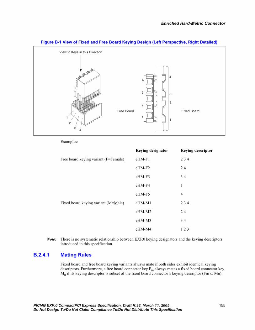
Enriched Hard-Metric Connector
Figure B-1 View of Fixed and Free Board Keying Design (Left Perspective, Right Detailed)
Examples:
Keying designator Keying descriptor
Free board keying variant (F=Female) eHM-F1 2 3 4
eHM-F2 2 4
eHM-F3 3 4
eHM-F4 1
eHM-F5 4
Fixed board keying variant (M=Male) eHM-M1 2 3 4
eHM-M2 2 4
eHM-M3 3 4
eHM-M4 1 2 3
Note: There is no systematic relationship between EXP.0 keying designators and the keying descriptors introduced in this specification.
B.2.4.1 Mating Rules
Fixed board and free board keying variants always mate if both sides exhibit identical keying descriptors. Furthermore, a free board connector key Fm always mates a fixed board connector key Mn if its keying descriptor is subset of the fixed board connector’s keying descriptor (Fm ⊂ Mn).
1
4
2
3
Free Board Fixed Board
View to Keys in this Direction
4
3
2
1
4
3
2
1
PICMG EXP.0 CompactPCI Express Specification, Draft R.93, March 11, 2005 155Do Not Design To/Do Not Claim Compliance To/Do Not Distribute This Specification
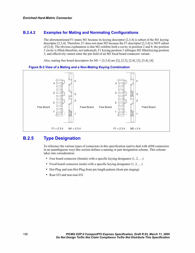
Enriched Hard-Metric Connector
B.2.4.2 Examples for Mating and Nonmating Configurations
The aforementioned F1 mates M1 because its keying descriptor [2,3,4] is subset of the M1 keying descriptor [2,3,4]. Therefore, F1 does not mate M2 because the F1 descriptor [2,3,4] is NOT subset of [2,4]. The obvious explanation is that M2 exhibits both a cavity in position 2 and 4; the position 3 cavity is filled (therefore, not indicated). F1 keying position 3 infringes M2 filled keying position 3, and effectively cannot enter the pin field of an M2 fixed board connector variant.
Also, mating free board descriptors for M1 = [2,3,4] are [2], [2,3], [2,4], [3], [3,4], [4].
Figure B-2 View of a Mating and a Non-Mating Keying Combination
B.2.5 Type DesignationTo reference the various types of connectors in this specification (and to deal with eHM connectors in an unambiguous way) this section defines a naming or part designation scheme. This scheme takes into consideration:
• Free board connector (female) with a specific keying designator (1, 2, …)
• Fixed board connector (male) with a specific keying designator (1, 2, …)
• Hot-Plug and non-Hot-Plug front pin length pattern (front pin staging)
• Rear-I/O and non-rear-I/O
4
3
2
1
4
3
2
1
Free Board Fixed Board
M1 = 2 3 4F1 = 2 3 4
4
3
2
1
4
3
2
1
Free Board Fixed Board
M2 = 2 4F1 = 2 3 4
156 PICMG EXP.0 CompactPCI Express Specification, Draft R.93, March 11, 2005Do Not Design To/Do Not Claim Compliance To/Do Not Distribute This Specification

Enriched Hard-Metric Connector
Part designation of eHM connectors shall be done according to following scheme:
Examples:
• Backplane Hot-Plug version (for non-Rear I/O application) with key designator #1 eHM-M1-HP
• Daughter card connector with key designator #5 eHM-F5
Note: This naming scheme intentionally disregards features beyond the scope of this specification (for example, different press-fit length and PCB termination methods).
B.2.6 Applicational Information
B.2.6.1 Alignment and Gathering
As with standard IEC HM B-modules, the eHM connectors have no alignment features. To maintain correct mating, the eHM connectors should be accompanied by at least one appropriate connector with an alignment feature, as with standard IEC HM A-modules, IEC HM AB-modules, or PICMG ADF connectors. In this specification, this is the Hybrid Slot comprising the HM A-module. For System Slot, Type 1 Slot, and Type 2 Slot, the ADF connector includes effective alignment.
Together, these connectors accomplish the free board/fixed board interface. IEC terminology refers this as “complete connector.”
Contact Type(F(emale), M(ale)/Free Board Connector, Fixed Board Connector)
Keying Designator(1...5)
Staging(HP = Hot-Plug)(Empty for Free Board Connectors)
Rear Extension(RX = Rear Extension)(Empty for Free Board Connectors)
eHM-<Gender> <Keying Descriptor> - <Staging> - <Rear Extension>
PICMG EXP.0 CompactPCI Express Specification, Draft R.93, March 11, 2005 157Do Not Design To/Do Not Claim Compliance To/Do Not Distribute This Specification

Enriched Hard-Metric Connector
B.2.6.2 Polarization
eHM fixed board connectors implement the same trapezoidal polarization feature in their base plate as do standard IEC HM connectors. Therefore, the connector pin position 1 side can join the end of such a standard connector to avoid false placement.
Refer to Figure B-4 for a visual representation of this feature.
B.3 Dimensional InformationNote: Dimensions in this appendix are in millimeters (mm).
B.3.1 General
B.3.2 View and Common FeaturesFigure B-3 View of Fixed and Free Board Connectors
158 PICMG EXP.0 CompactPCI Express Specification, Draft R.93, March 11, 2005Do Not Design To/Do Not Claim Compliance To/Do Not Distribute This Specification

Enriched Hard-Metric Connector
Figure B-4 View of Fixed Board Connector Including Polarization Feature
B.3.3 Remarks on Mating Properties of eHM ConnectorThe connector design adopts all required mating conditions from the ADF connector instead of the standard IEC connectors, because the ADF connector’s properties are more restrictive.
Mating conditions to be applied:
Perpendicular to engagement direction: Vertical misalignment ±1.38 mmHorizontal misalignment ±1.30 mm
Inclination: 2.0°
Polarization Feature
PICMG EXP.0 CompactPCI Express Specification, Draft R.93, March 11, 2005 159Do Not Design To/Do Not Claim Compliance To/Do Not Distribute This Specification

Enriched Hard-Metric Connector
B.3.4 Fixed Board Connector
B.3.4.1 Dimensions
Figure B-5 Dimensional Drawing of Fixed Board eHM Connector
160 PICMG EXP.0 CompactPCI Express Specification, Draft R.93, March 11, 2005Do Not Design To/Do Not Claim Compliance To/Do Not Distribute This Specification
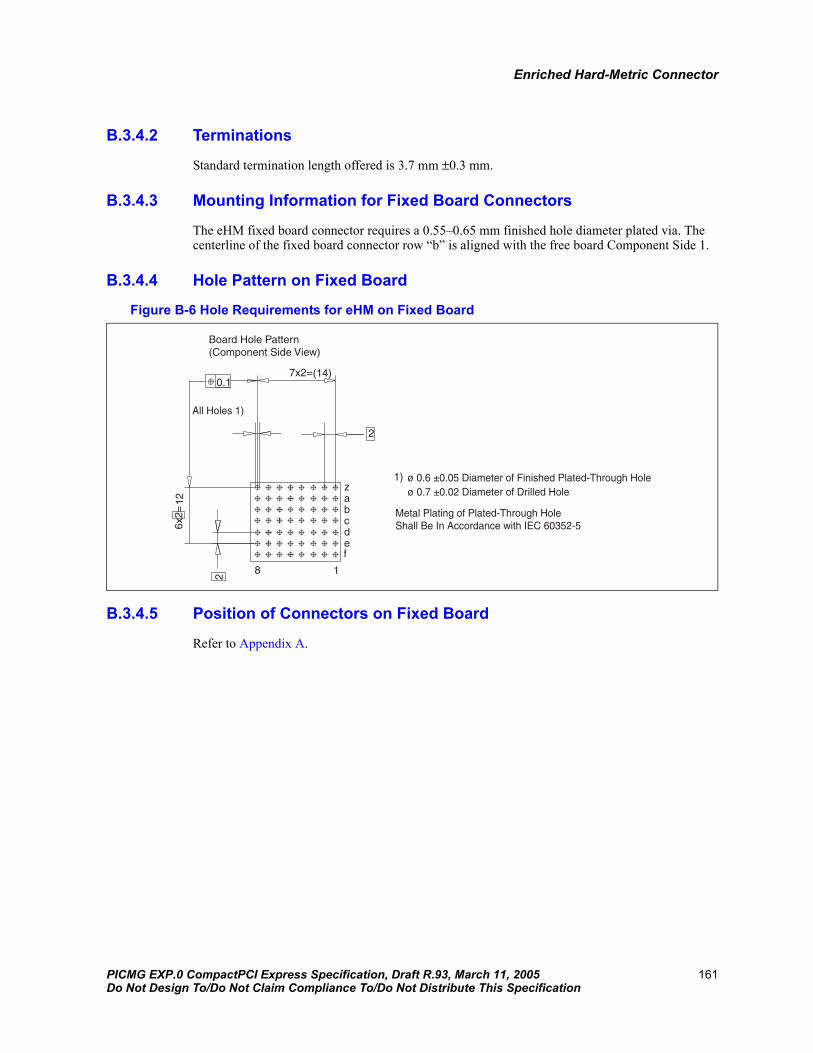
Enriched Hard-Metric Connector
B.3.4.2 Terminations
Standard termination length offered is 3.7 mm ±0.3 mm.
B.3.4.3 Mounting Information for Fixed Board Connectors
The eHM fixed board connector requires a 0.55–0.65 mm finished hole diameter plated via. The centerline of the fixed board connector row “b” is aligned with the free board Component Side 1.
B.3.4.4 Hole Pattern on Fixed Board
Figure B-6 Hole Requirements for eHM on Fixed Board
B.3.4.5 Position of Connectors on Fixed Board
Refer to Appendix A.
Metal Plating of Plated-Through HoleShall Be In Accordance with IEC 60352-5
ø 0.6 ±0.05 Diameter of Finished Plated-Through Holeø 0.7 ±0.02 Diameter of Drilled Hole
1)
edcba
18
0.1
All Holes 1)
126x
2=
2
(14)7x2=
2
z
f
Board Hole Pattern(Component Side View)
PICMG EXP.0 CompactPCI Express Specification, Draft R.93, March 11, 2005 161Do Not Design To/Do Not Claim Compliance To/Do Not Distribute This Specification
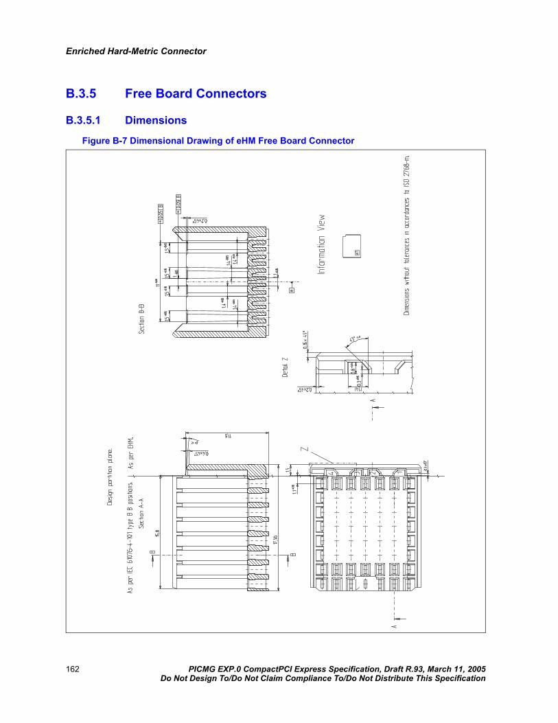
Enriched Hard-Metric Connector
B.3.5 Free Board Connectors
B.3.5.1 Dimensions
Figure B-7 Dimensional Drawing of eHM Free Board Connector
162 PICMG EXP.0 CompactPCI Express Specification, Draft R.93, March 11, 2005Do Not Design To/Do Not Claim Compliance To/Do Not Distribute This Specification
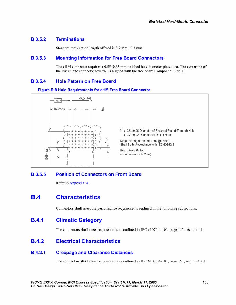
Enriched Hard-Metric Connector
B.3.5.2 Terminations
Standard termination length offered is 3.7 mm ±0.3 mm.
B.3.5.3 Mounting Information for Free Board Connectors
The eHM connector requires a 0.55–0.65 mm finished hole diameter plated via. The centerline of the Backplane connector row “b” is aligned with the free board Component Side 1.
B.3.5.4 Hole Pattern on Free Board
Figure B-8 Hole Requirements for eHM Free Board Connector
B.3.5.5 Position of Connectors on Front Board
Refer to Appendix A.
B.4 CharacteristicsConnectors shall meet the performance requirements outlined in the following subsections.
B.4.1 Climatic CategoryThe connectors shall meet requirements as outlined in IEC 61076-4-101, page 157, section 4.1.
B.4.2 Electrical Characteristics
B.4.2.1 Creepage and Clearance Distances
The connectors shall meet requirements as outlined in IEC 61076-4-101, page 157, section 4.2.1.
abcde
18
0.1
1.5
All Holes 1)
Board Hole Pattern(Component Side View)
105x
2= 2
(14)7x2=
2
f
Metal Plating of Plated-Through HoleShall Be In Accordance with IEC 60352-5
ø 0.6 ±0.05 Diameter of Finished Plated-Through Holeø 0.7 ±0.02 Diameter of Drilled Hole
1)
PICMG EXP.0 CompactPCI Express Specification, Draft R.93, March 11, 2005 163Do Not Design To/Do Not Claim Compliance To/Do Not Distribute This Specification
Enriched Hard-Metric Connector
B.4.2.2 Voltage Proof
The connectors shall meet requirements as outlined in IEC 61076-4-101, page 159, section 4.2.2.
B.4.2.3 Current-Carrying Capacity
The connectors shall meet requirements as outlined in IEC 61076-4-101, page 159, section 4.2.3.
B.4.2.4 Contact Resistance
The connectors shall meet requirements as outlined in IEC 61076-4-101, page 161, section 4.2.4.
B.4.2.5 Insulation Resistance
The connectors shall meet requirements as outlined in IEC 61076-4-101, page 161, section 4.2.5.
B.4.3 Mechanical
B.4.3.1 Mechanical Operation
The connectors shall meet requirements as outlined in IEC 61076-4-101, page 161, section 4.3.1.
B.4.3.2 Engaging and Separating Forces
The connectors shall meet requirements as outlined in IEC 61076-4-101, page 161, section 4.3.2.
B.4.3.3 Contact Retention in Insert
The connectors shall meet requirements as outlined in IEC 61076-4-101, page 163, section 4.3.3.
B.4.3.4 Static Load, Transverse
The connectors shall meet requirements as outlined in IEC 61076-4-101, page 163, section 4.3.4.
B.4.3.5 Gauge Retention Force
The connectors shall meet requirements as outlined in IEC 61076-4-101, page 163, section 4.3.5.
B.4.3.6 Vibration (Sinusoidal)
The connectors shall meet requirements as outlined in IEC 61076-4-101, page 163, section 4.3.6.
B.4.3.7 Shock
The connectors shall meet requirements as outlined in IEC 61076-4-101, page 165, section 4.3.7.
164 PICMG EXP.0 CompactPCI Express Specification, Draft R.93, March 11, 2005Do Not Design To/Do Not Claim Compliance To/Do Not Distribute This Specification

Enriched Hard-Metric Connector
B.4.3.8 Polarization Method
Not applicable.
B.4.3.9 Robustness and Effectiveness of Coding Device
B.4.3.9.1 Conditions According to IEC60512-7, Test 13e
The eHM connector pair to be tested shall be mounted in a fixture that guarantees a sufficient degree of guidance according to following conditions:
Misalignment perpendicular to engagement direction: Vertical ±0.5 mmHorizontal ±0.5 mm
Inclination: Transverse and longitudinal ±2.0°
Each single keying element pair (respective elements on the free and fixed board connectors) that does not mate shall withstand a force of 50 N without damage on the fixed or free board connector side. In a blocked situation, there shall be no electrical contact between any male contact (of any level) and any female contact.
B.5 Test ScheduleRefer to IEC 61076-4-101, page 167, section 5.
B.6 Quality Assessment ProceduresRefer to IEC 61076-4-101, page 185, section 6.
PICMG EXP.0 CompactPCI Express Specification, Draft R.93, March 11, 2005 165Do Not Design To/Do Not Claim Compliance To/Do Not Distribute This Specification

Universal Power Connector (UPM)
Universal Power Connector (UPM) C
C.1 General DataIn accordance with PICMG Policies and Procedures, Tyco Electronics Corp.has committed to grant licenses under reasonable and nondiscriminatory terms to the intellectual property of those companies necessary to manufacture the UPM connectors for PICMG applications. Tyco does not warrant that the license conveyed is sufficient to manufacture the connector without infringing the intellectual property rights of third parties.
C.1.1 Objective of this DocumentThis specification is not intended to provide enough information to allow for tooling and manufacturing of the UPM connector. It serves only as a specification for the key features and characteristics that the UPM connectors used in the CompactPCI Express specification shall meet.
166 PICMG EXP.0 CompactPCI Express Specification, Draft R.93, March 11, 2005Do Not Design To/Do Not Claim Compliance To/Do Not Distribute This Specification

Universal Power Connector (UPM)
C.2 DimensionsFigure C-1 UPM-F-7 Female 7-Position Power Connector Dimensional Information
MATERIAL: HOUSING: POLYESTER, GRAY. CONTACT: PHOSPHOR BRONZE
FINISH: CONTACT MATING AREA: 1.27 µm MINIMUM GOLD PLATE. ACTION PIN AREA, 0.5 µm MINIMUM TIN-LEAD PLATE. ALL OVER 1.27 µm MINIMUM NICKEL UNDERPLATE.
DIMENSION APPLIES AFTER CONNECTOR IS APPLIED TO PC BOARD.
DIMENSIONS ARE IN MILLIMETERS.
UNLESS OTHERWISE SPECIFIED, ALL TWO-PLACE DIMENSIONS SHALL HAVE A TOLERANCE OF ± 0.13 mm.
1
1
TYPE DESIGNATION: UPM-F-7
PICMG EXP.0 CompactPCI Express Specification, Draft R.93, March 11, 2005 167Do Not Design To/Do Not Claim Compliance To/Do Not Distribute This Specification

Universal Power Connector (UPM)
Figure C-2 UPM-F-5 Female 5-Position Power Connector Dimensional Information
Figure C-3 Male 7-Position Power Connector Dimensional Information
MATERIAL: HOUSING: POLYESTER, GRAY. CONTACT: PHOSPHOR BRONZE.
FINISH: CONTACT MATING AREA: 1.27 µm MINIMUM GOLD PLATE. ACTION PIN AREA, 0.5 µm MINIMUM TIN-LEAD PLATE. ALL OVER 1.27 µm MINIMUM NICKEL UNDERPLATE.
DIMENSION APPLIES AFTER CONNECTOR IS APPLIED TO PC BOARD.
DIMENSIONS ARE IN MILLIMETERS.
UNLESS OTHERWISE SPECIFIED, ALL TWO-PLACE DIMENSIONS SHALL HAVE A TOLERANCE OF ± 0.13 mm.
1
1
TYPE DESIGNATION: UPM-F-5
HOUSING: POLYESTER, GRAY.CONTACT: PHOSPHOR BRONZE.
CONTACT: MATING AREA: 1.27 µm MIN GOLD PLATE.ACTION PIN AREA: 0.5 µm MIN TIN-LEAD PLATE.ALL OVER 1.27 µm MIN NICKEL UNDERPLATE.
CONTACT LUBRICATION WITH BELCORE APPROVEDLUBRICANT. TECHNICAL REFERENCE: TR-NWT-001217ISSUE 1, SEPT 1992.
DIMENSIONS ARE IN MILLIMETERS.
UNLESS OTHERWISE SPECIFIED, ALL TWO-PLACE DIMENSIONS SHALL HAVE A TOLERANCE OF ± 0.13 mm.
TYPEDESIGNATION
HOT-PLUGCOMPATIBLE
BLADE LENGTHS ATEACH POSITION
UPM-M-7-HP
UPM-M-7
YES
NO
DIM ADIM BDIM ADIM B
A B C D E F G14.6011.3811.3814.6011.3811.3814.6010.90 7.68 7.68 10.90 7.68 7.68 10.9014.6014.6014.6014.6014.6014.6014.6010.9010.9010.9010.9010.9010.9010.90
168 PICMG EXP.0 CompactPCI Express Specification, Draft R.93, March 11, 2005Do Not Design To/Do Not Claim Compliance To/Do Not Distribute This Specification

Universal Power Connector (UPM)
Figure C-4 UPM-M-5 Male 5-Position Power Connector Dimensional Information
C.3 Perpendicular to Engagement DirectionThe front board connectors will accommodate a vertical misalignment of 1.15 mm and a horizontal misalignment of 1.62 mm.
C.4 InclinationThe permitted angular misalignment accommodated by the connector is 2.0 mm from the perpendicular in both transverse and longitudinal axes.
C.5 Mounting InformationFigure C-5 Hole Pattern for 7-Row Male UPM Power Connector
HOUSING: POLYESTER, GRAY.CONTACT: PHOSPHOR BRONZE.
CONTACT: MATING AREA: 1.27 µm MIN GOLD PLATE.ACTION PIN AREA: 0.5 µm MIN TIN-LEAD PLATE.ALL OVER 1.27 µm MIN NICKEL UNDERPLATE.
CONTACT LUBRICATION WITH BELCORE APPROVEDLUBRICANT. TECHNICAL REFERENCE: TR-NWT-001217ISSUE 1, SEPT 1992.
DIMENSIONS ARE IN MILLIMETERS.
UNLESS OTHERWISE SPECIFIED, ALL TWO-PLACE DIMENSIONS SHALL HAVE A TOLERANCE OF ± 0.13 mm.
BLADE LENGTHS ATEACH POSITION
UPM-M-5 DIM ADIM B
A B C D ETYPE
DESIGNATION14.6010.90
14.6014.6014.6014.6010.9010.9010.9010.90
PICMG EXP.0 CompactPCI Express Specification, Draft R.93, March 11, 2005 169Do Not Design To/Do Not Claim Compliance To/Do Not Distribute This Specification

Universal Power Connector (UPM)
Figure C-6 Hole Pattern for 5-Row Male UPM Power Connector
Figure C-7 Hole Pattern for Female 7-Row UPM Power Connector
170 PICMG EXP.0 CompactPCI Express Specification, Draft R.93, March 11, 2005Do Not Design To/Do Not Claim Compliance To/Do Not Distribute This Specification

Universal Power Connector (UPM)
Figure C-8 Hole Pattern for Female 5-Row UPM Power Connector
C.6 Climatic CategoryTests shall be performed at ambient environment conditions as per IEC-60512.
Table C-1 Climatic Category
Test Description Requirement Procedure
Examination of product. Meets requirements of product drawing.
Visual, dimensional, and functional per applicable quality inspection plan.IEC 60512-1-1 Test 1a
ELECTRICAL
Termination resistance. 10 mΩ maximum. EIA 364-23A.Alternate: IEC 60512-2-1 Test 2aSubject mated contacts assembled in housing to 20 mV maximum open circuit at 100 mA maximum.
Insulation resistance. 10000 MΩ minimum. EIA 364-21CAlternate: IEC 60512-3-1 Test 3aTest between adjacent contacts of mated samples.
Dielectric withstanding voltage. 1000 V AC at sea level.1 minute hold.No breakdown or flashover.
IEC 60512-4-1 Test 4aTest between adjacent contacts of mated samples.
PICMG EXP.0 CompactPCI Express Specification, Draft R.93, March 11, 2005 171Do Not Design To/Do Not Claim Compliance To/Do Not Distribute This Specification

Universal Power Connector (UPM)
Temperature rise vs current. 30 °C maximum temperature rise at specified current.
EIA 364-70AAlternate IEC 60512-5-1 Test 5aEnergize all contacts with 15 A.
MECHANICAL
Vibration, sinusoidal. No discontinuities of 1 µs or longer duration.See Note.
EIA 364-28D, Test Condition II Alternate: IEC 60512-6-4 Test 6dSubject mated samples to 10-500-10 Hz traversed in 11.25 min with 0.71 mm total excursion or 5 G, whichever is less. 2 hours in each of 3 mutually perpendicular planes.
Mechanical shock. No discontinuities of 1 µs or longer duration.See Note.
EIA 364-27B, Method AAlternate: IEC 60512-6-3 Test 6cSubject mated samples to 50 G half-sine shock pulses of 11 ms duration. 5 shocks in each direction applied along 3 mutually perpendicular planes, 30 total shocks.
Durability. See Note. EIA 364-9CAlternate: IEC 60512-5 Test 9aMate and unmate samples for 250 cycles at a maximum rate of 325 cycles per hour. Note: 250 cycles equals PL 2 for HM.
Contact retention. Axial displacement shall not exceed 0.2 mm with force applied or 0.1 mm after force has been removed.
EIA 364-29BAlternate: IEC 60512-8 Test 15aApply axial force of 10 N to pin contacts in the unmating direction at a maximum rate of 2.54 mm per minute and hold for 5 s.Apply axial force of 5 N to pin contacts in the mating direction at a maximum rate of 2.54 mm per minute and hold for 5 s.Apply axial force of 5 N to receptacle contacts in both the mating and unmating directions at a maximum rate of 2.54 mm per minute and hold for 5 s.
Mating force. 1 N per contact maximum. IEC 60512-13-1 Test 13aMeasure force necessary to mate samples at a maximum rate of 25.4 mm per minute.
Unmating force. 0.5 N per contact minimum. IEC 60512-13-1 Test 13aMeasure force necessary to unmate samples at a maximum rate of 25.4 mm per minute.
Test Description Requirement Procedure
172 PICMG EXP.0 CompactPCI Express Specification, Draft R.93, March 11, 2005Do Not Design To/Do Not Claim Compliance To/Do Not Distribute This Specification

Universal Power Connector (UPM)
Termination strength.Note: In IEC 60512, called “Robustness of termination.”
See Note. EIA 364-62Alternate: IEC 60512-8 Test 16fApply axial force of 10 N to plug contacts in both the mating and unmating directions at a maximum rate of 2.54 mm per minute and hold for 10 s.
Static load, transverse. See Note. IEC60512–5 Test 8aA 25 N side-to-side load and a 50 N front-to-back load shall be applied to unmated plug and receptacles using a 3 mm rod with rounded end. Load shall be applied in the middle of the plug and receptacle modules approximately 6 mm and 11 mm above the printed circuit board.
ENVIRONMENTAL
Thermal shock. See Note. EIA 364-32CAlternate: IEC 60512-11-4 Test 11dSubject mated samples to 5 cycles between –55 and 125 °C.
Humidity, steady state. See Note. EIA 364-31B, Method IIAlternate: IEC 60512-11-3 Test 11cSubject samples to 56 days at 40°C and 93% RH with 60 VDC applied between adjacent contacts.
Humidity-temperature cycling. See Note. EIA 364-31B, Method IIIAlternate: IEC 60512-11-12 Test 11mSubject samples to 6 24-hour cycles of humidity-temperature cycling. A cycle consists of the following: Transition from 25 °C and 95% RH to 55 °C and 90% RH in 3 h. Dwell at 55 °C and 90% RH for 9 h. Transition from 55 °C and 90% RH to 25 °C and 80% RH in 3 h. Dwell at 25 °C and 95% RH for 9 h. At the end of the first cycle, remove samples from chamber and precondition at –55 °C for 2 h. Place samples in an altitude chamber and subject all adjacent contact pairs to 200 VAC for 1 min at a simulated altitude of 30000 ft.
Test Description Requirement Procedure
PICMG EXP.0 CompactPCI Express Specification, Draft R.93, March 11, 2005 173Do Not Design To/Do Not Claim Compliance To/Do Not Distribute This Specification

Universal Power Connector (UPM)
Note: Connectors shall meet visual requirements and show no physical damage.
Electrical load, high temperature. See Note. IEC 60512-11-9 Test 11iSubject mated samples with thermocouples attached and energized at 7.8 A to oven temperature of 70 °C. Increase oven temperature until internal sample temperature stabilizes at 125 °C. Maintain temperature for 1000 h.
Temperature life. See Note. IEC 60512-11-9 Test 11iSubject mated samples to 125 °C for 16 h.
Industrial atmosphere. See Note. IEC 60512-11-7 Test 11g Method 1Subject 4 mated and 4 unmated samples to 10 days exposure in a 500 PPM concentration of sulphur dioxide and a 100 PPM concentration of hydrogen sulfide at 25 °C and 75% RH.
Test Description Requirement Procedure
174 PICMG EXP.0 CompactPCI Express Specification, Draft R.93, March 11, 2005Do Not Design To/Do Not Claim Compliance To/Do Not Distribute This Specification