pim in pcbs: mechanisms & mitigation - isola group · on the same pcb reverse pim can vary by...
TRANSCRIPT
© 2015 Isola Group & its subsidiaries. All rights reserved. © 2015 Isola Group & its subsidiaries. All rights reserved. 1
PIM in PCBs: Mechanisms & Mitigation
© 2015 Isola Group & its subsidiaries. All rights reserved. © 2015 Isola Group & its subsidiaries. All rights reserved.
Outline Introduction & Definitions PIM Sources & Physical Mechanisms in
Communication Systems Methods of Measuring PIM Sources of PIM in PCBs PIM Mitigation & Guidelines for Low
PIM in PCBs
© 2015 Isola Group & its subsidiaries. All rights reserved. © 2015 Isola Group & its subsidiaries. All rights reserved.
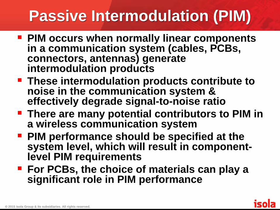
Passive Intermodulation (PIM) PIM occurs when normally linear components
in a communication system (cables, PCBs, connectors, antennas) generate intermodulation products These intermodulation products contribute to
noise in the communication system & effectively degrade signal-to-noise ratio There are many potential contributors to PIM in
a wireless communication system PIM performance should be specified at the
system level, which will result in component-level PIM requirements For PCBs, the choice of materials can play a
significant role in PIM performance
© 2015 Isola Group & its subsidiaries. All rights reserved. © 2015 Isola Group & its subsidiaries. All rights reserved.
Passive Intermodulation (PIM)
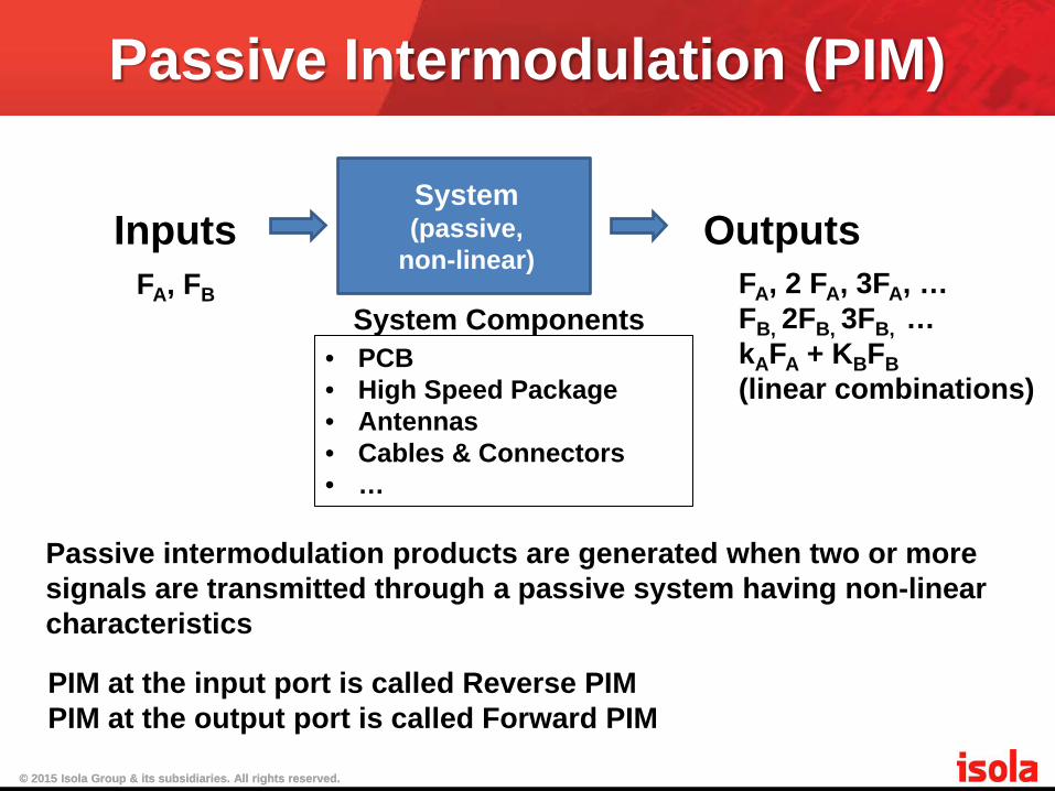
Inputs Outputs System (passive,
non-linear)
• PCB • High Speed Package • Antennas • Cables & Connectors • …
System Components FA, FB FA, 2 FA, 3FA, …
FB, 2FB, 3FB, … kAFA + KBFB (linear combinations)
Passive intermodulation products are generated when two or more signals are transmitted through a passive system having non-linear characteristics
PIM at the input port is called Reverse PIM PIM at the output port is called Forward PIM

© 2015 Isola Group & its subsidiaries. All rights reserved. © 2015 Isola Group & its subsidiaries. All rights reserved.
Passive Intermodulation (PIM)
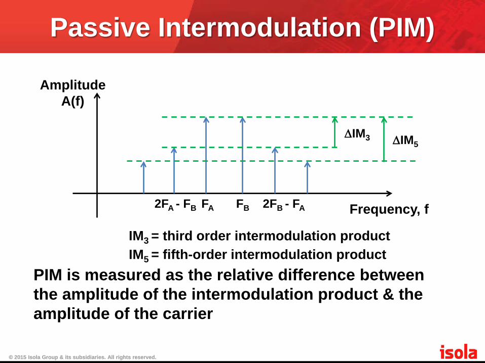
FA FB 2FB - FA 2FA - FB
∆IM3
Frequency, f
Amplitude A(f)
IM3 = third-order intermodulation product
PIM is measured as the relative difference between the amplitude of the intermodulation product & the amplitude of the carrier
© 2015 Isola Group & its subsidiaries. All rights reserved. © 2015 Isola Group & its subsidiaries. All rights reserved.
Passive Intermodulation (PIM)
FA FB 2FB - FA 2FA - FB
∆IM3
Frequency, f
Amplitude A(f)
IM3 = third order intermodulation product
∆IM5
IM5 = fifth-order intermodulation product
PIM is measured as the relative difference between the amplitude of the intermodulation product & the amplitude of the carrier
© 2015 Isola Group & its subsidiaries. All rights reserved. © 2015 Isola Group & its subsidiaries. All rights reserved.
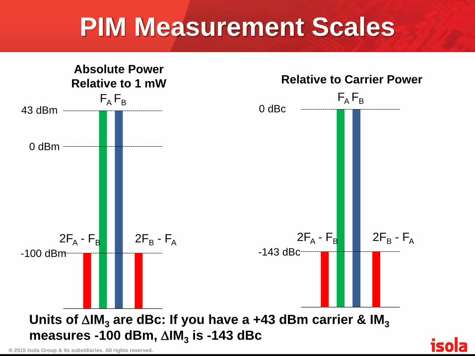
PIM Measurement Scales
FA FB
2FA - FB 2FB - FA
Absolute Power Relative to 1 mW Relative to Carrier Power
43 dBm
-100 dBm
0 dBm
FA FB
2FA - FB 2FB - FA
0 dBc
-143 dBc
Units of ∆IM3 are dBc: If you have a +43 dBm carrier & IM3 measures -100 dBm, ∆IM3 is -143 dBc
© 2015 Isola Group & its subsidiaries. All rights reserved. © 2015 Isola Group & its subsidiaries. All rights reserved.
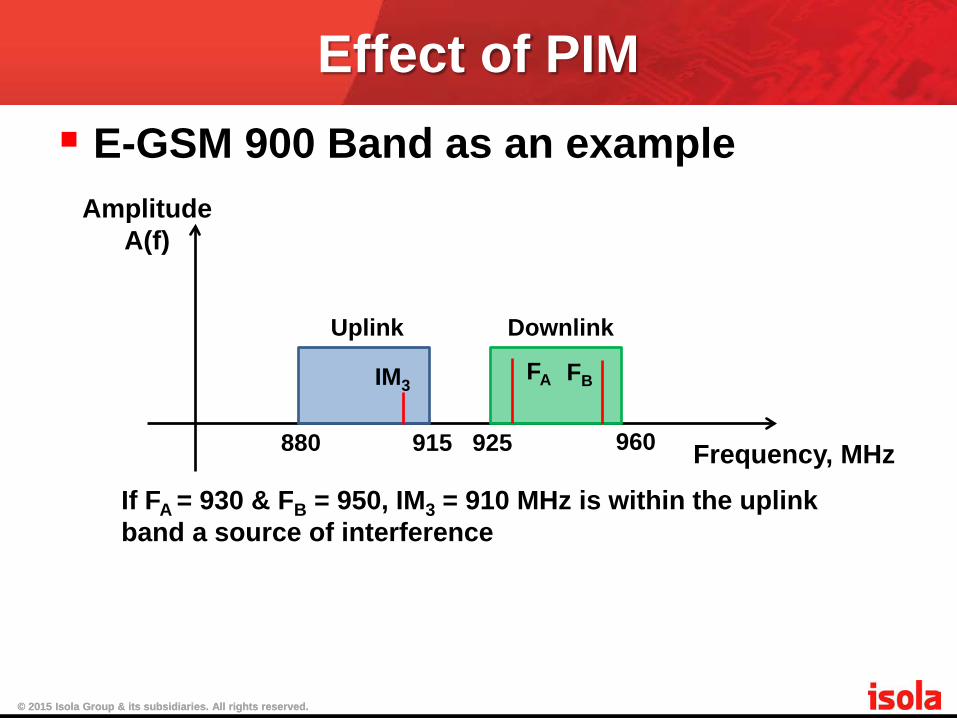
Effect of PIM E-GSM 900 Band as an example
If FA = 930 & FB = 950, IM3 = 910 MHz is within the uplink band a source of interference
Frequency, MHz
Amplitude A(f)
Uplink Downlink
925 960 915 880
IM3 FA FB
© 2015 Isola Group & its subsidiaries. All rights reserved. © 2015 Isola Group & its subsidiaries. All rights reserved.
PIM Bandwidth When carriers are modulated, as is the case for
spread spectrum, transmitted signals have a finite bandwidth Intermodulation products have bandwidths
multiplied by their product number—IM3 has 3x bandwidth of carrier, etc. Result is wideband noise rather than isolated
effects near the modulation frequency, with contributors (IM3, IM5, etc.) overlapping in frequency Frequency management prevents some PIM
from falling within desired signal band but often is unavoidable
© 2015 Isola Group & its subsidiaries. All rights reserved. © 2015 Isola Group & its subsidiaries. All rights reserved.
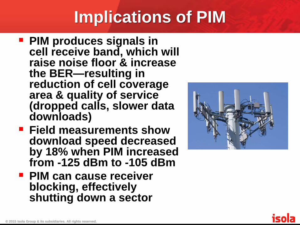
Implications of PIM PIM produces signals in
cell receive band, which will raise noise floor & increase the BER—resulting in reduction of cell coverage area & quality of service (dropped calls, slower data downloads) Field measurements show
download speed decreased by 18% when PIM increased from -125 dBm to -105 dBm PIM can cause receiver
blocking, effectively shutting down a sector

© 2015 Isola Group & its subsidiaries. All rights reserved. © 2015 Isola Group & its subsidiaries. All rights reserved.
PIM Sources & Physical Mechanisms in Communication Systems
© 2015 Isola Group & its subsidiaries. All rights reserved. © 2015 Isola Group & its subsidiaries. All rights reserved.
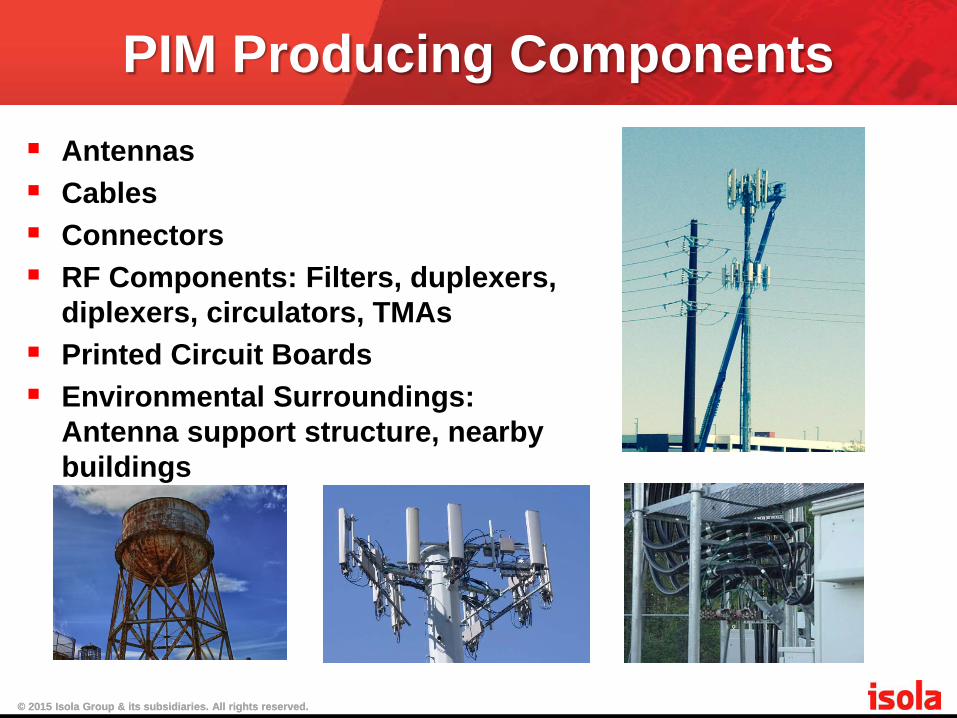
PIM Producing Components Antennas Cables Connectors RF Components: Filters, duplexers,
diplexers, circulators, TMAs Printed Circuit Boards Environmental Surroundings:
Antenna support structure, nearby buildings

© 2015 Isola Group & its subsidiaries. All rights reserved. © 2015 Isola Group & its subsidiaries. All rights reserved.
PIM Sources Ferromagnetic materials (ferrites, nickel,
steel, etc.) due to Hysteresis effect Contaminates including dirt, moisture or
oxides on electrically conducting surfaces Inconsistent metal-to-metal contact Unmatched (galvanically) metals in contact Multipath with oxidized metal structures Stray metal particles from component
installation of cable fabrication In PCBs, non-linear trace resistance & non-
linear dielectric properties
© 2015 Isola Group & its subsidiaries. All rights reserved. © 2015 Isola Group & its subsidiaries. All rights reserved.
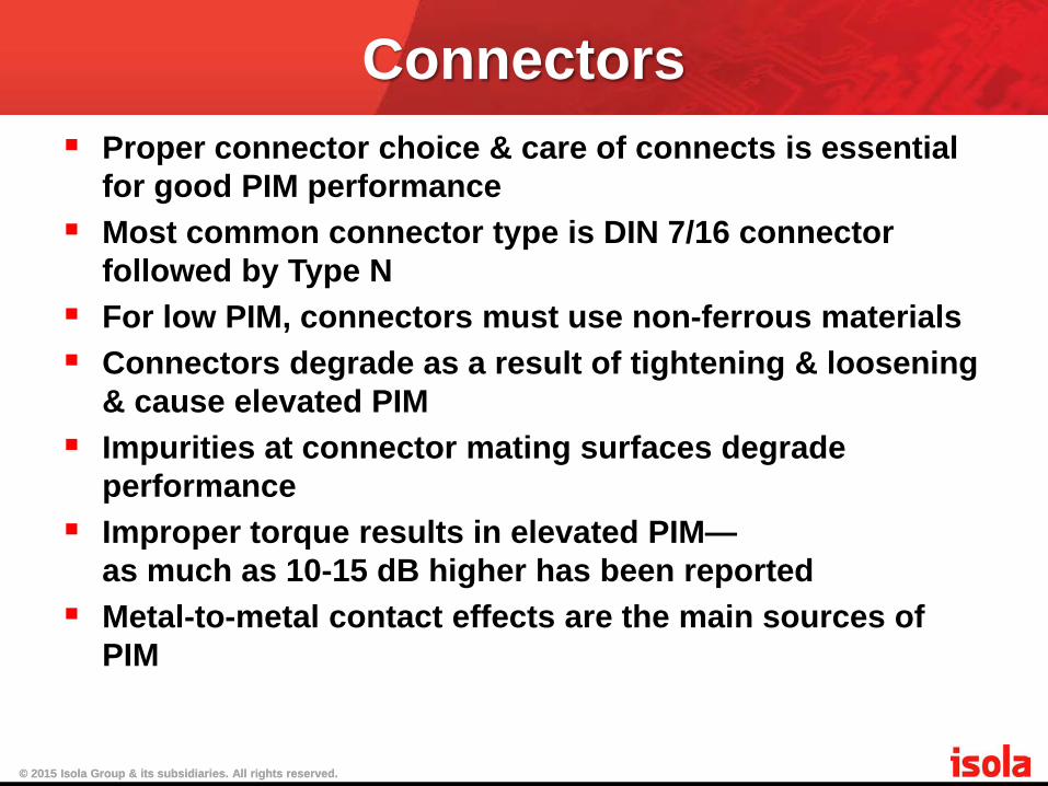
Connectors Proper connector choice & care of connects is essential
for good PIM performance Most common connector type is DIN 7/16 connector
followed by Type N For low PIM, connectors must use non-ferrous materials Connectors degrade as a result of tightening & loosening
& cause elevated PIM Impurities at connector mating surfaces degrade
performance Improper torque results in elevated PIM—
as much as 10-15 dB higher has been reported Metal-to-metal contact effects are the main sources of
PIM

© 2015 Isola Group & its subsidiaries. All rights reserved. © 2015 Isola Group & its subsidiaries. All rights reserved.
PIM Physical Mechanisms
© 2015 Isola Group & its subsidiaries. All rights reserved. © 2015 Isola Group & its subsidiaries. All rights reserved.
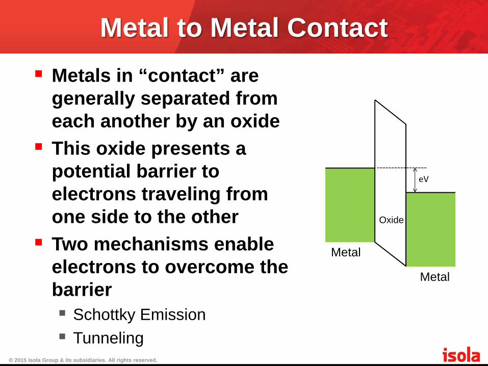
Metal to Metal Contact Metals in “contact” are
generally separated from each another by an oxide This oxide presents a
potential barrier to electrons traveling from one side to the other Two mechanisms enable
electrons to overcome the barrier Schottky Emission Tunneling
Metal
Metal
Oxide
© 2015 Isola Group & its subsidiaries. All rights reserved. © 2015 Isola Group & its subsidiaries. All rights reserved.
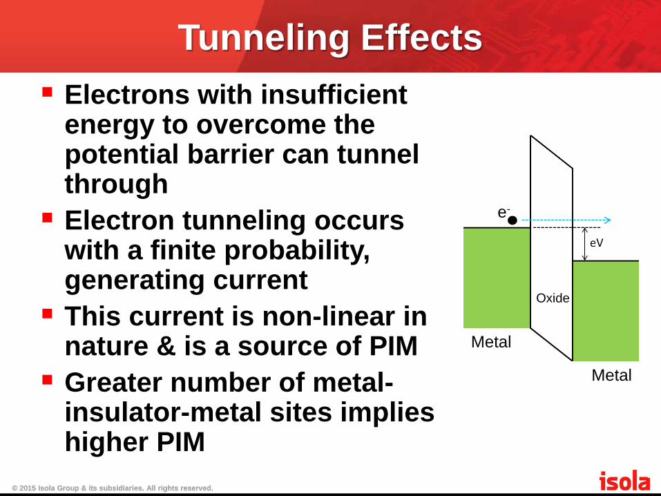
Tunneling Effects Electrons with insufficient
energy to overcome the potential barrier can tunnel through Electron tunneling occurs
with a finite probability, generating current This current is non-linear in
nature & is a source of PIM Greater number of metal-
insulator-metal sites implies higher PIM
Metal
Metal
Oxide
e-
© 2015 Isola Group & its subsidiaries. All rights reserved. © 2015 Isola Group & its subsidiaries. All rights reserved.
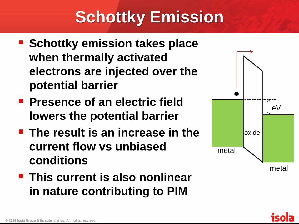
Schottky Emission
eV
metal
metal
oxide
Schottky emission takes place when thermally activated electrons are injected over the potential barrier Presence of an electric field
lowers the potential barrier The result is an increase in the
current flow vs unbiased conditions This current is also nonlinear
in nature contributing to PIM
© 2015 Isola Group & its subsidiaries. All rights reserved. © 2015 Isola Group & its subsidiaries. All rights reserved.
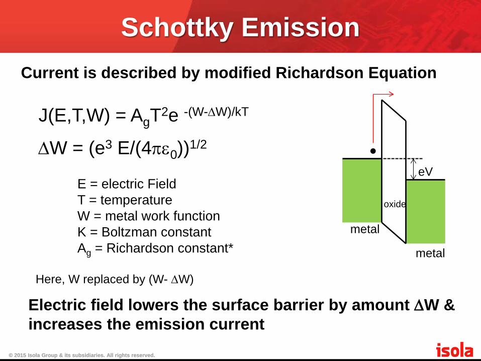
Schottky Emission
Electric field lowers the surface barrier by amount ∆W & increases the emission current
J(E,T,W) = AgT2e -(W-∆W)/kT
∆W = (e3 E/(4πε0))1/2
Here, W replaced by (W- ∆W)
E = electric Field T = temperature W = metal work function K = Boltzman constant Ag = Richardson constant*
eV
metal
metal
oxide
Current is described by modified Richardson Equation
© 2015 Isola Group & its subsidiaries. All rights reserved. © 2015 Isola Group & its subsidiaries. All rights reserved.
Constriction Resistance Constriction resistance results when
current flows through a limited area between two metallic contacts Localized heating occurs as a result of
the current bunching & changes the resistance The change in resistance is a non-
linear effect & contributes to PIM

© 2015 Isola Group & its subsidiaries. All rights reserved. © 2015 Isola Group & its subsidiaries. All rights reserved.
PIM Testing
© 2015 Isola Group & its subsidiaries. All rights reserved. © 2015 Isola Group & its subsidiaries. All rights reserved.
Measurements IEC 62037 is the PIM measurement standard Two tones at 43 dBm (20W) each are injected into the device
under test & magnitudes of IM products are measured Measurements are typically performed in shielded enclosure to
prevent interference but are also done in the field on cell towers
Equipment Kaelus (Summitek) Instruments PIM analyzer Anritsu PIM Master
High quality coax to microstrip transitions are required to evaluate PIM performance of PCB laminates
On the same PCB Reverse PIM can vary by 10dB based on the transition type – cable launch vs edge connector
Near-field field-probe is alternate test method
© 2015 Isola Group & its subsidiaries. All rights reserved. © 2015 Isola Group & its subsidiaries. All rights reserved.
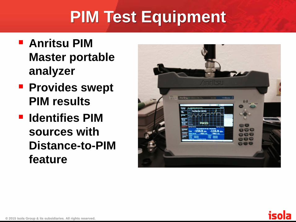
PIM Test Equipment Anritsu PIM
Master portable analyzer Provides swept
PIM results Identifies PIM
sources with Distance-to-PIM feature
© 2015 Isola Group & its subsidiaries. All rights reserved. © 2015 Isola Group & its subsidiaries. All rights reserved.
Reverse PIM Testing For reverse PIM testing, two signals are sent
to antenna & PIM levels are measured at same test port Most commonly, one of two signals is swept
in frequency to avoid signal cancellation at a single frequency In the field, care must be taken with swept
measurements so interference with service subscribers doesn’t occur This is the most common PIM testing
© 2015 Isola Group & its subsidiaries. All rights reserved. © 2015 Isola Group & its subsidiaries. All rights reserved.
Forward PIM Testing For forward PIM, signals are transmitted through antenna
system & receive antenna & spectrum analyzer are used For improved accuracy & isolation tests on antennas are
often performed in anechoic chamber Forward PIM measurements are not susceptible to
cancellation when done in controlled environment Forward PIM not typically measured for installed antenna
systems in field such as base station Forward PIM is also performed using a high rejection
filter network on the output of the device under test to separate out PIM components
Forward PIM tests are used to characterize PCB features responsible for PIM

© 2015 Isola Group & its subsidiaries. All rights reserved. © 2015 Isola Group & its subsidiaries. All rights reserved.
Sources of PIM in PCBs
© 2015 Isola Group & its subsidiaries. All rights reserved. © 2015 Isola Group & its subsidiaries. All rights reserved.
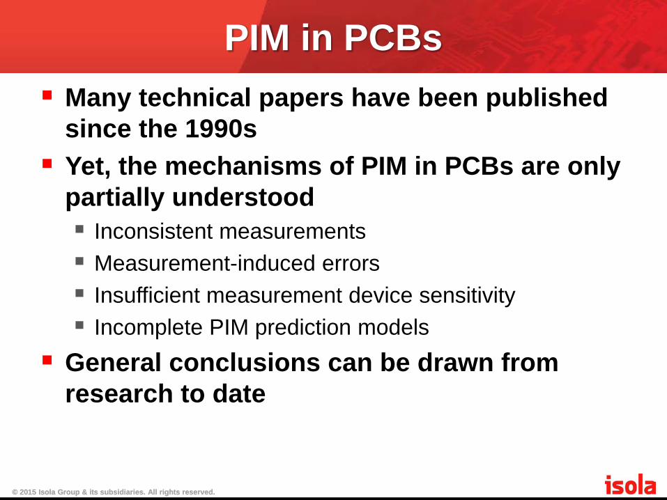
PIM in PCBs Many technical papers have been published
since the 1990s Yet, the mechanisms of PIM in PCBs are only
partially understood Inconsistent measurements Measurement-induced errors Insufficient measurement device sensitivity Incomplete PIM prediction models
General conclusions can be drawn from research to date

© 2015 Isola Group & its subsidiaries. All rights reserved. © 2015 Isola Group & its subsidiaries. All rights reserved.
General Conclusions Forward PIM in PCBs is considered a distributed
non-linearity and is cumulative Magnitude monotonically increases with transmission line length
Forward PIM decreases with increasing trace width Decrease in current density is believed responsible for this effect
Reverse PIM unaffected by line length and trace width but affected by input/output transmission line mismatch Results of cable launch vs DIN 7/16 connectors illustrate effect
Reverse PIM is generally lower than forward PIM PIM performance can be traced to physical
characteristics of PCBs elements
© 2015 Isola Group & its subsidiaries. All rights reserved. © 2015 Isola Group & its subsidiaries. All rights reserved.
PIM in PCBs Quality of Copper Etched Trace Quality and Uniformity Dielectric Composition
© 2015 Isola Group & its subsidiaries. All rights reserved. © 2015 Isola Group & its subsidiaries. All rights reserved.
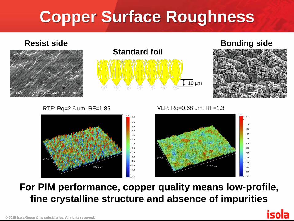
Copper Surface Roughness Resist side Bonding side
Standard foil
~10 µm
RTF: Rq=2.6 um, RF=1.85 VLP: Rq=0.68 um, RF=1.3
For PIM performance, copper quality means low-profile, fine crystalline structure and absence of impurities
© 2015 Isola Group & its subsidiaries. All rights reserved. © 2015 Isola Group & its subsidiaries. All rights reserved.
Etched Trace Quality Quality of etching strongly affects PIM
performance Rough and fractured edges of a trace
can create sites for contamination Poor quality edges create voids and
can degrade the finish coating Trace width variations can increase
non-linear thermo-resistance effects
© 2015 Isola Group & its subsidiaries. All rights reserved. © 2015 Isola Group & its subsidiaries. All rights reserved.
Dielectric Composition Materials of various compositions and
ranges of Dk, Df have been measured to assess impact on PIM General conclusions from research indicate Materials with high moisture absorption have worse
PIM performance Presence of fillers can increase PIM Dielectric materials with lower Df tend to have lower
PIM but is more of a secondary effect vs the effects of copper traces Change in crystallinity associated with PTFE-based
laminates is bad for PIM stability over time
© 2015 Isola Group & its subsidiaries. All rights reserved. © 2015 Isola Group & its subsidiaries. All rights reserved.
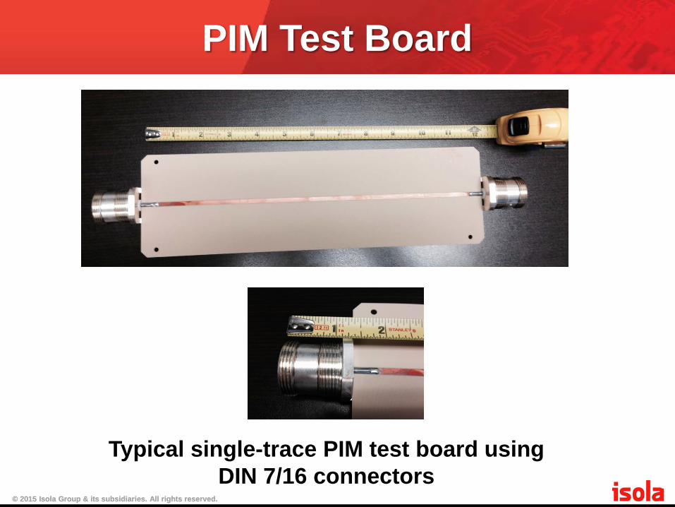
PIM Test Board
Typical single-trace PIM test board using DIN 7/16 connectors

© 2015 Isola Group & its subsidiaries. All rights reserved. © 2015 Isola Group & its subsidiaries. All rights reserved.
PIM Mitigation in PCBs
© 2015 Isola Group & its subsidiaries. All rights reserved. © 2015 Isola Group & its subsidiaries. All rights reserved.
Mitigating PIM in PCBs Choose low-profile copper Rough copper is more prone to defect trapping & non-
linear thermo-electric effects Use thicker copper than you might ordinarily use
while maintaining low profile Better thermal performance, fewer non-linear thermal
resistive effects Use laminates with low dielectric loss & those
without ceramic fillers—some are ferroelectric Use “PIM-friendly” finish coating such as
immersion tin To achieve good PIM performance over time, avoid
PTFE-based products Optimize circuit layout to minimize PIM generation Minimize sharp bends in traces and features causing
current to concentrate
© 2015 Isola Group & its subsidiaries. All rights reserved. © 2015 Isola Group & its subsidiaries. All rights reserved.
Fabrication Concerns Using the same base materials,
different fabricators can yield circuit boards having vastly different PIM performance There are two major contributors to the
differences seen Etch quality of lines Introduction of impurities
These risks can be mitigated through proper quality control
© 2015 Isola Group & its subsidiaries. All rights reserved. © 2015 Isola Group & its subsidiaries. All rights reserved.
References “Understanding PIM Application Note”, Anritsu, http://www.anritsu.com/en-
US/Products-Solutions/Solution/Understanding-PIM.aspx Nash, Adrian, “Intermodulation Distortion Problems at UMTS Cell Sites”, Aeroflex
Wireless Test Solutions, Burnham Jargon, Jeffrey A., DeGroot, Donald C., Reed, Kristopher L., “NIST Passive
Intermodulation Measurement Comparison for Wireless Base Station Equipment”, 52nd ARFTG Conf. Digest, pp. 128-139, Rohnert Park, CA, Dec 3-4, 1998.
Shitvov, A., Olson, T., Schuchinsky, A., “Current Progress in Phenomenology & Experimental Characterization of Passive Intermodulation in Printed Circuits”
Shitvov, A., Olson, T., Schuchinsky, A., “Effect of Laminate Properties on Passive Intermodulation Generation”
Shitvov, A., Zelenchuk, D., Olson, T., Schuchinsky, A., “Transmission/Reflection Measurements & Near-Field Mapping Techniques for Passive Intermodulation Characterization of Printed Lines”
Shitvov, A., Zelenchuk, D., Schuchinsky, A., Fusco, V., “Passive Intermodulation in Printed Lines: Effects of Trace Dimensions & Substrate”, IET Microw. & Antennas Propag., 2009, Vol. 3, Iss 2, pp. 260-268
Crowell, C. R. (1965). "The Richardson constant for thermionic emission in Schottky barrier diodes". Solid-State Electronics 8 (4): 395–399. Bibcode:1965SSEle...8..395C. doi:10.1016/0038-1101(65)90116-4.
Orloff, J. (2008). "Schottky emission". Handbook of Charged Particle Optics (2nd ed.). CRC Press. pp. 5–6. ISBN 978-1-4200-4554-3.