pll design essentials for wireless systems - … 900 class-4 small ms ... • use the same design...
TRANSCRIPT

PLL Design Essentialsfor
Wireless Systems
Derek K. Shaeffer, [email protected]
Beceem Communications, Inc.

PLL Design Essentials for Wireless SystemsDerek K. Shaeffer, Ph.D.
2
Overview• In this talk, we will attempt to answer the following:
– What types of system-level issues set wireless terminal performance requirements?
– How are wireless terminals typically specified in standards-based systems?
– Which specifications are germane to the frequency synthesizer?
– How do I translate wireless terminal standards into a relevant set of synthesizer specifications?
– What is a “toolkit” of useful modeling techniques and / or theorems that I can use to calculate expected performance and evaluate tradeoffs?

PLL Design Essentials for Wireless SystemsDerek K. Shaeffer, Ph.D.
3
Outline•• Understanding wireless systems Understanding wireless systems
specificationsspecifications–– The wireless channel and the issues it raisesThe wireless channel and the issues it raises–– Common performance specification types and Common performance specification types and
techniquestechniques• Developing frequency synthesizer
specifications– Bandwidth, stability and settling behavior – Noise theorems and modeling techniques– Spectral impurity modeling and performance
calculation• Summary

PLL Design Essentials for Wireless SystemsDerek K. Shaeffer, Ph.D.
4
Wireless Channel Attributes• The wireless channel is a fading multipath channel, producing:
– Large-scale, slow signal fades (shadow fading)– Small-scale, rapid signal fades (Rayleigh fading)– A time-varying impulse response– Pulse spreading in time (Delay spread)– Spectral spreading in frequency (Doppler spread)
• Time-variance is present, whether or not the mobile terminal is in motion, due to inevitable motion of other objects
• Basically, it’s a wonder that reliable communication is even possible on such a channel
• Bottom line– Your signal is often weak– The other guy’s signal is often strong– Need to minimize interference potential and maximize link margin

PLL Design Essentials for Wireless SystemsDerek K. Shaeffer, Ph.D.
5
Some Important Interference Modes• Direct interference due to
finite filter stop-band attenuation
• Spill-over caused by TX spectral impurities– TX LO phase noise– TX spectral regrowth
• Reciprocal mixing caused by RX local oscillator spectral impurities– RX LO phase noise– RX LO spurious
• Also RX compression and IMD (not shown)
Direct Interference
Spill-Over
Reciprocal Mixing

PLL Design Essentials for Wireless SystemsDerek K. Shaeffer, Ph.D.
6
Transmitter Spectral Purity
Standard Qty Raster Level BW Bands
GSM 5 200 kHz < -36 dBm 100 kHz MS Rx & BS Rx
Bluetooth 3 1 MHz < -20 dBm 1 MHz All
Transmitter Spectral Purity Allowable Exceptions (Spurious)
-20
0
-40
P (dBc / dBm)
550
2,00
0
3,00
0 Δf
Bluetooth Class-3100-kHz Meas. BW
(dBc)1-MHz Meas. BW
(dBm)0.5
-30-33
-60-63-65-71
-79 dBm
P (dBc)
30-kHz Meas. BW 100-kHz Meas. BW
100
200
250
400
1,80
0
3,00
0
6,00
0
20,0
00Δf
GSM 900 Class-4 MS
-67 dBm
600
EDGE
-54
10,0
00
Note: 0 dBc corresponds to30-kHz Meas. BW on-channel
widebandnoise
spectralregrowth
widebandnoise
spectralregrowth

PLL Design Essentials for Wireless SystemsDerek K. Shaeffer, Ph.D.
7
Receiver Selectivity
Standard Qty Raster Level Bands
GSM 6 / 24 200 kHz > -43 dBm In-Band / OOB
Bluetooth 5 / 24 1 MHz > 17 dBc / -50 dBm IB (> 2MHz) / OOB
Receiver Selectivity Exceptions (Spurious Response)
-10
-27
-71
P (dBm)
1,00
0
2,00
0
3,00
0 Δf
Bluetooth Class-3
402,
000
-60
-30
Desired signal atSensitivity + 10dB
w/ modulated blocker
Desired signal atSensitivity + 3dB
modulated blocker (in-band)CW blocker (out-of-band)
recip mix
spillover / spurs
filtering (OOB)
0
-23
-33
-43
-73
-91
P (dBm)
Desired signal atSensitivity + 20dB
w/ modulated blocker
Desired signal atSensitivity + 3dBw/ CW blocker
200
600
400
800
1,60
0
3,00
0
20,0
00
Δf
GSM 900 Class-4 Small MS
recip mix
spillover / spurs
filtering (OOB)
-41
PLL Design Essentials for Wireless SystemsDerek K. Shaeffer, Ph.D.
8
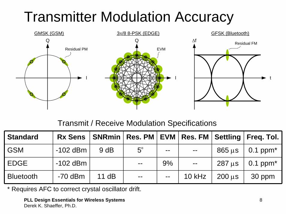
Transmitter Modulation Accuracy
Standard Rx Sens SNRmin Res. PM EVM Res. FM Settling Freq. Tol.
GSM -102 dBm 9 dB 5º -- -- 865 μs 0.1 ppm*
EDGE -102 dBm -- 9% -- 287 μs 0.1 ppm*
Bluetooth -70 dBm 11 dB -- -- 10 kHz 200 μs 30 ppm
Transmit / Receive Modulation Specifications
* Requires AFC to correct crystal oscillator drift.
t
Δf Residual FM
GFSK (Bluetooth)
I
Q3π/8 8-PSK (EDGE)
EVM
I
QGMSK (GSM)
Residual PM

PLL Design Essentials for Wireless SystemsDerek K. Shaeffer, Ph.D.
9
Outline• Understanding wireless systems
specifications– The wireless channel and the issues it raises– Common performance specification types and
techniques•• Developing frequency synthesizer Developing frequency synthesizer
specificationsspecifications–– Bandwidth, stability and settling behaviorBandwidth, stability and settling behavior–– Noise theorems and modeling techniquesNoise theorems and modeling techniques–– Spectral impurity modeling and performance Spectral impurity modeling and performance
calculationcalculation• Summary
PLL Design Essentials for Wireless SystemsDerek K. Shaeffer, Ph.D.
10
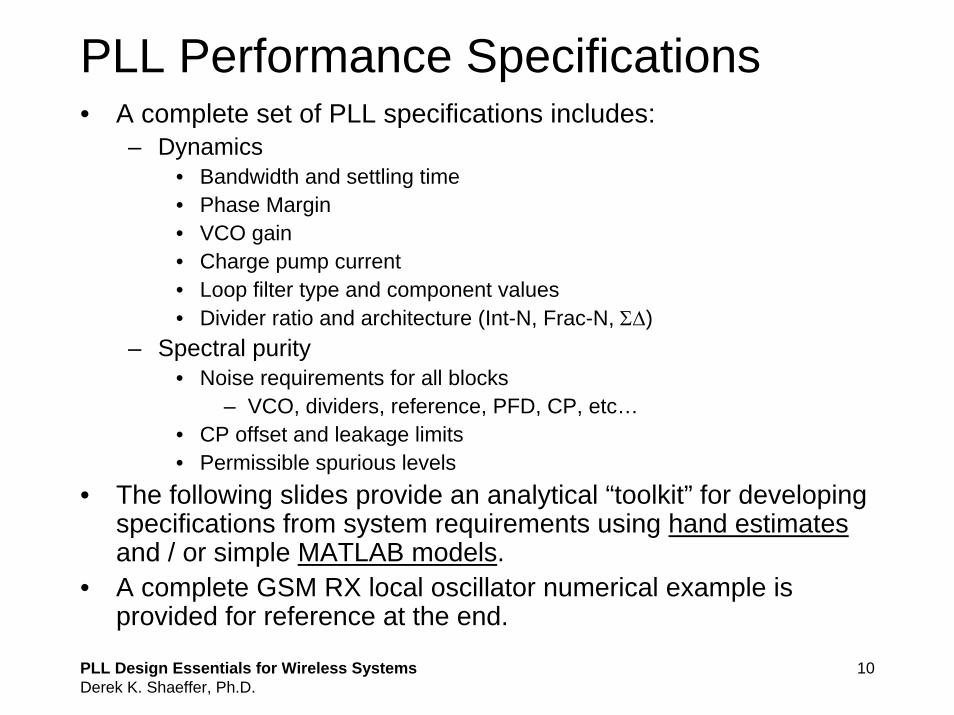
PLL Performance Specifications• A complete set of PLL specifications includes:
– Dynamics• Bandwidth and settling time• Phase Margin• VCO gain• Charge pump current• Loop filter type and component values• Divider ratio and architecture (Int-N, Frac-N, ΣΔ)
– Spectral purity• Noise requirements for all blocks
– VCO, dividers, reference, PFD, CP, etc…• CP offset and leakage limits• Permissible spurious levels
• The following slides provide an analytical “toolkit” for developing specifications from system requirements using hand estimatesand / or simple MATLAB models.
• A complete GSM RX local oscillator numerical example is provided for reference at the end.

A Typical Wireless PLL
• SD Fractional-N Loop– Fine frequency resolution & support for multiple crystal frequencies
• Coarse Tuning– Minimize Kvco to keep spurious under control
• Kvco Compensation– Maintain loop dynamics over VCO fine-tuning range
• Freq. Conversion– For direct-conversion systems, VCO is off-frequency
PLL Design Essentials for Wireless SystemsDerek K. Shaeffer, Ph.D.
11

Phase-Domain Representation
• Linear model is approximately valid provided that fC < fREF/10.• N is the average divider modulus.• The ΣΔ modulator produces noise that is shaped away from DC.
– This noise needs to be rejected by the loop filter H(s)
• For a constant reference frequency, φin is a ramp.
PLL Design Essentials for Wireless SystemsDerek K. Shaeffer, Ph.D.
12

PLL Design Essentials for Wireless SystemsDerek K. Shaeffer, Ph.D.
13
3rd-Order Type-II PLL Dynamics
f
dB(T)
f
phase(T)
P.M.
0
fC
fC
-20 dB/dec
fC/kL
fC*kL
fC/kL fC*kL
-40 dB/dec
-40 dB/dec
up
dn
C1C2
R
VCO
fREF
fOUTPFD CP
/ N
( ) ( )ssH
NCKIsT
LP
VCOCP=( )
⎟⎟⎠
⎞⎜⎜⎝
⎛+
+=
P
Z
ss
s
ssH
ω
ω
1
1
2
2/1
P.M.sin1P.M.sin1
⎥⎦⎤
⎢⎣⎡−+
=Lk
KVCO in Hz/V
21 CCCLP +=
12
1
2 −= LkCC
Bode Plots
Loop Transmission Expressions
LCZ kff =
LCP kff ⋅=
LP
VCOCP
L
C
NCKI
k=
2ω
Specify: ωC and P.M.
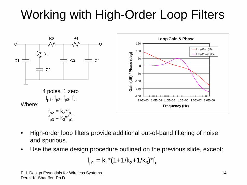
Working with High-Order Loop Filters
• High-order loop filters provide additional out-of-band filtering of noise and spurious.
• Use the same design procedure outlined on the previous slide, except:
PLL Design Essentials for Wireless SystemsDerek K. Shaeffer, Ph.D.
14
-200
-150
-100
-50
0
50
100
150
1.0E+03 1.0E+04 1.0E+05 1.0E+06 1.0E+07 1.0E+08
Gai
n (d
B) /
Pha
se (d
eg)
Frequency (Hz)
Loop Gain & Phase
Loop Gain (dB)
Loop Phase (deg)
4 poles, 1 zerofp1, fp2, fp3, fz
Where: fp2 = k2*fp1fp3 = k3*fp1
fp1 = kL*(1+1/k2+1/k3)*fc
PLL Design Essentials for Wireless SystemsDerek K. Shaeffer, Ph.D.
15
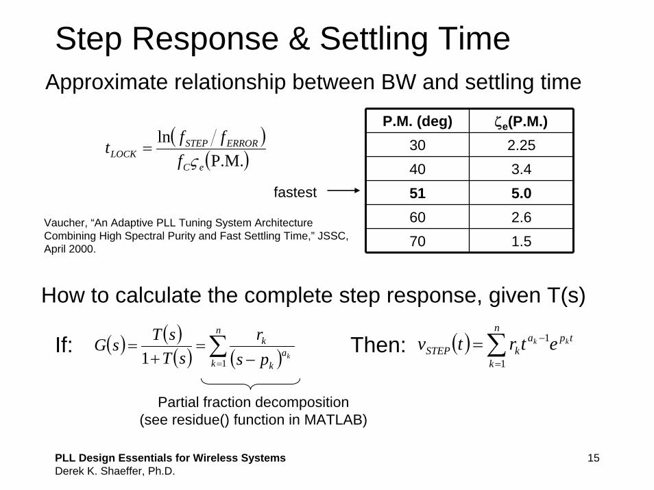
Step Response & Settling TimeApproximate relationship between BW and settling time
( )( )P.M.
ln
eC
ERRORSTEPLOCK f
fftς
=
P.M. (deg) ζe(P.M.)30 2.2540 3.451 5.060 2.670 1.5
fastest
Vaucher, “An Adaptive PLL Tuning System Architecture Combining High Spectral Purity and Fast Settling Time,” JSSC, April 2000.
How to calculate the complete step response, given T(s)
( ) ( )( ) ( )∑
= −=
+=
n
ka
k
kkps
rsT
sTsG11
If: ( ) ∑=
−=n
k
tpakSTEP
kk etrtv1
1Then:
Partial fraction decomposition(see residue() function in MATLAB)

PLL Design Essentials for Wireless SystemsDerek K. Shaeffer, Ph.D.
16
Watch Out: Limits of Linear Analysis• Linear analysis should always be
supplemented with time-domain simulations• To minimize settling time, avoid:
– Cycle slipping• Large frequency steps can over-range the PFD
– VCO overload• AFC techniques are commonly used to reduce VCO gain• A low-gain VCO, desirable for noise immunity, may
require high gain CP / LF• Loop filter transients can overload the tuning port of the
VCO and / or saturate the CP output

PLL Design Essentials for Wireless SystemsDerek K. Shaeffer, Ph.D.
17
Sources of Spectral Impurity• Noise
– VCO phase noise– Divider jitter– Noise coupling from other circuits
• Spurious– CP leakage– CP up / down current mismatch– Fractional divider spurs
• Noise and spurs refer to the PLL output via the signal transfer function (STF) and noise transfer function (NTF) of the loop.

PLL Design Essentials for Wireless SystemsDerek K. Shaeffer, Ph.D.
18
Modeling block-level noise contribs• VCO
– Typically have 1/f3, 1/f2 and flat noise asymptotes
– 1/f3 corner not equal to process 1/f corner
• See Hajimiri & Lee reference• Reference, dividers, etc…
– Typically need to include 1/f corner, esp. in CMOS
– Dividers, PFD will require Spectre or HB simulation to estimate noise / power tradeoffs
• Low Frequency Limit– Spectral density levels off at low
frequencies so that the total integrated power equals the carrier power.
L(f)
Low-frequency limit
Typical Divider SSB Phase Noise PSD
-10 dB/dec
fLF
ff1
f
L(f)
f2f3
-30 dB/dec
-20 dB/dec
Low-frequency limit
Typical VCO SSB Phase Noise PSD
fLF
1/f3 corner
1/f2 corner
1/f corner

Conventional PFD / CP Topology
• PFD reset path incorporates a delay, TMIN, which sets a minimum pulsewidth for the CP.
• This delay eliminates the ‘dead-zone’ due to runt CP pulses.
PLL Design Essentials for Wireless SystemsDerek K. Shaeffer, Ph.D.
19
UP
DN
TMIN
t
Ref. Late
UP
DNt
Ref. Early
TMINUP
DNt
LockedTMIN
TMIN
IOUT
2
-2
ICP
ICP
ICP
ICP
IOUT
TMIN
D Q
R
D Q
R
Ref
Div
UP
DN
PLL Design Essentials for Wireless SystemsDerek K. Shaeffer, Ph.D.
20
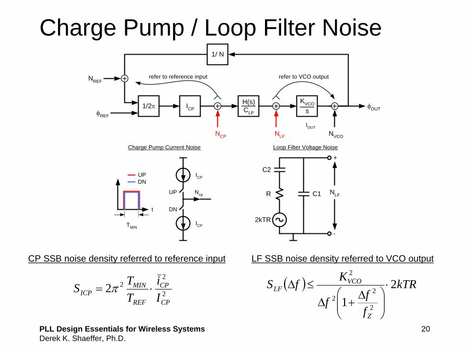
Charge Pump / Loop Filter Noise
2
222
CP
CP
REF
MINICP I
iTTS ⋅= π ( ) kTR
fff
KfS
Z
VCOLF 2
1 2
22
2
⋅
⎟⎟⎠
⎞⎜⎜⎝
⎛ Δ+Δ
≤Δ
CP SSB noise density referred to reference input LF SSB noise density referred to VCO output
ICP
1/ N
1/2πφREF
NREF
IOUT
φOUTH(s)CLP
KVCO
s
NVCONLFNCP
refer to reference input refer to VCO output
DN
UP
ICP
ICP
Ncp
DNUP
t
Charge Pump Current Noise Loop Filter Voltage Noise
C1
C2
R
+
NLF
-
2kTRTMIN

PLL Design Essentials for Wireless SystemsDerek K. Shaeffer, Ph.D.
21
Spurious Tones: CP Leakage
• Reference spurious level (dBc) at offset Δf from carrier is partly determined by charge pump leakage current as a percentage of the charge pump current (η).
( ) ( )
⎥⎥⎥⎥⎥
⎦
⎤
⎢⎢⎢⎢⎢
⎣
⎡
⎟⎟⎠
⎞⎜⎜⎝
⎛ Δ+
⎟⎟⎠
⎞⎜⎜⎝
⎛ Δ+
⎟⎟⎠
⎞⎜⎜⎝
⎛Δ
=⎥⎦
⎤⎢⎣
⎡ΔΔ
=Δ 2
2
2
1010
1
12log20log20
CL
C
L
C
L
VCOHLEAK
fkf
ffk
ff
kN
fKfZI
fS πη
DN
UP
ICP
ICP
IOUT
DNUP
t
phase error
TREF
Area=TREFILEAK
t
ILEAK
-ILEAK
ICPArea=TREFILEAK
IOUT
CP
LEAK
II
=η

PLL Design Essentials for Wireless SystemsDerek K. Shaeffer, Ph.D.
22
Spurious Tones: CP Mismatch
• Reference spurious due to CP mismatch is in quadrature with leakage spur, depending mainly on the UP / DN current mismatch (δ) and the minimum UP / DN pulsewidth (TMIN).
−ΔICP
TMIN
ICP
Area=TMINΔICP
Area=TMINΔICP
t
IOUT
DN
UP
ICP
ICP+ΔICP
IOUT
DNUP
t
phase error
( ) ( )
⎥⎥⎥⎥⎥
⎦
⎤
⎢⎢⎢⎢⎢
⎣
⎡
⎟⎟⎠
⎞⎜⎜⎝
⎛ Δ+
⎟⎟⎠
⎞⎜⎜⎝
⎛ Δ+
⎟⎟⎠
⎞⎜⎜⎝
⎛Δ
=⎥⎦
⎤⎢⎣
⎡ΔΔ
⋅Δ⋅=Δ 2
2
2
2
22
102
2
10
1
12log20log20
CL
C
L
C
REF
MIN
L
VCOH
REF
MINCP
fkf
ffk
ff
TT
kN
fKfZ
TTIfS δππ
CP
CP
IIΔ
=δ

CP Nonlinearity – Noise Folding
• CP Nonlinearity causes SD quantization noise to fall in-band.– Note the non-zero mean of CP current PDF.– Implies degraded residual P.M. due to noise folding to low frequencies.
• After folding, this noise cannot be rejected by the loop filter.
PLL Design Essentials for Wireless SystemsDerek K. Shaeffer, Ph.D.
23C
P C
urre
nt P
DF

Mitigating CP Nonlinearity
• CP offset current– Increased noise– Reference spur
• PFD delay offset– Longer TMIN– No reference spur
PLL Design Essentials for Wireless SystemsDerek K. Shaeffer, Ph.D.
24
IOUT
IUP > IDN
New lock point
D Q
R
D Q
R
IOUT
IUP > IDN
Shifted inflection
point
TRef
Div
UP
DN
UP
DN
IUP
IDN
IL
IOUT
UP
DN
T
t

PLL Design Essentials for Wireless SystemsDerek K. Shaeffer, Ph.D.
25
3rd-Order Type-II PLL NTF / STF
• Noise sources can be referred to two points in the loop:– VCO output (VCO noise)– Reference input (Reference, PFD, CP, Divider)
• VCO noise is high-pass filtered by the loop noise transfer function• Reference noise is low-pass filtered by the loop signal transfer function
-40 dB/dec
f
dB(STF)
fC
fC/kL fC*kL
0 dBdB(NTF)
40 dB/dec
φOUTICP
1/ N
NVCO
H(s)CLP
1/2πφREF
NREF
KVCO
s
( ) ( )( )sTsNTsSTF
+=
1
( ) ( )sTsNTF
+=
11
( ) ( ) ( ) ( ) ( ) 22 sNTFsNsSTFsNsN VCOREFOUT ⋅+⋅=
…where T(s) is the PLL loop transmission

PLL Design Essentials for Wireless SystemsDerek K. Shaeffer, Ph.D.
26
Residual PM and Residual FM
( )∫ ΔΔ=H
L
f
f
fdfL22φσ
( )∫ ΔΔΔ=H
L
f
ff fdfLf 22 2σ
Residual P.M.
Residual F.M.
• For many systems, residual phase modulation contributes to RX SNR reduction– Reference noise tends to dominate
• For FM systems (incl. Bluetooth), residual frequency modulation is more relevant– Broadband (VCO) noise is much more important
• Low-frequency integration limit is determined by the carrier recovery loop bandwidth
Offset Frequency (Hz)
fB
-10 dB/dec
-30 dB/dec
-20 dB/dec
f3 f2
PM (rad2/Hz) FM (Hz2/Hz)
-10 dB/dec10 dB/dec
20 dB/dec
PMFM
Typical PLL Noise PSD
PLL Design Essentials for Wireless SystemsDerek K. Shaeffer, Ph.D.
27
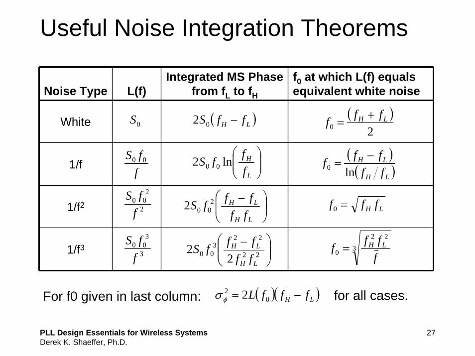
Useful Noise Integration Theorems
Noise Type L(f)Integrated MS Phase
from fL to fH
f0 at which L(f) equals equivalent white noise
White
1/f
1/f2
1/f3
0S
ffS 00
2
200
ffS
3
300
ffS
( )LH ffS −02
⎟⎟⎠
⎞⎜⎜⎝
⎛
L
H
fffS ln2 00
⎟⎟⎠
⎞⎜⎜⎝
⎛ −
LH
LH
fffffS 2
002
⎟⎟⎠
⎞⎜⎜⎝
⎛ −22
223
00 22
LH
LH
fffffS
( )20
LH fff +=
LH fff =0
( )( )LH
LH
fffff
ln0−
=
3
22
0 ffff LH=
( )( )LH fffL −= 02 2φσFor f0 given in last column: for all cases.

Optimal BW for Integrated Noise
PLL Design Essentials for Wireless SystemsDerek K. Shaeffer, Ph.D.
28
⎟⎟⎠
⎞⎜⎜⎝
⎛+=
BB
BBK opt
optJ2σ
Shaeffer, et al., “A 40 / 43-Gb/s SONET OC-768 SiGe 4:1 MUX / CMU,” ISSCC 2003

PLL Design Essentials for Wireless SystemsDerek K. Shaeffer, Ph.D.
29
Blocker Modeling• Blocker specifications contemplate different types of
interferers– CW (un-modulated) blockers– Modulated blockers within the same system– Modulated blockers from other systems
• Especially true in ISM bands, where different types of systems have to co-exist, sharing the same spectrum
• Need to generate PSD for each blocker type that is required for evaluating PLL performance– Use MATLAB to generate power spectra using random data– Fit the power spectrum to a piecewise linear or simple
functional representation for subsequent simulations– This is a good job for the systems guru in your group
PLL Design Essentials for Wireless SystemsDerek K. Shaeffer, Ph.D.
30
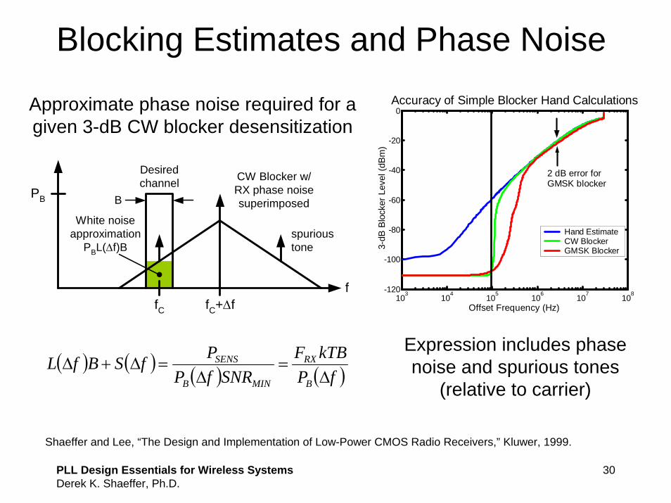
Blocking Estimates and Phase Noise
( ) ( ) ( ) ( )fPkTBF
SNRfPPfSBfL
B
RX
MINB
SENS
Δ=
Δ=Δ+Δ
Approximate phase noise required for a given 3-dB CW blocker desensitization
Shaeffer and Lee, “The Design and Implementation of Low-Power CMOS Radio Receivers,” Kluwer, 1999.
f
CW Blocker w/RX phase noisesuperimposed
fC
PB
fC+Δf
White noiseapproximation
PBL(Δf)B
Desiredchannel
B
spurioustone
Expression includes phase noise and spurious tones
(relative to carrier)
103 104 105 106 107 108-120
-100
-80
-60
-40
-20
0
Offset Frequency (Hz)
3-dB
Blo
cker
Lev
el (d
Bm)
Accuracy of Simple Blocker Hand Calculations
Hand EstimateCW BlockerGMSK Blocker
2 dB error forGMSK blocker
PLL Design Essentials for Wireless SystemsDerek K. Shaeffer, Ph.D.
31
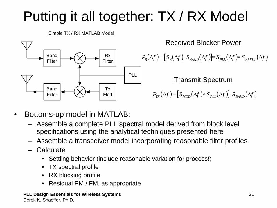
Putting it all together: TX / RX Model
• Bottoms-up model in MATLAB:– Assemble a complete PLL spectral model derived from block level
specifications using the analytical techniques presented here– Assemble a transceiver model incorporating reasonable filter profiles– Calculate
• Settling behavior (include reasonable variation for process!)• TX spectral profile• RX blocking profile• Residual PM / FM, as appropriate
( ) ( ) ( )[ ] ( ) ( )fSfSfSfSfP RXFLTPLLBANDBB Δ∗Δ∗Δ⋅Δ=Δ
Received Blocker Power
( ) ( ) ( )[ ] ( )fSfSfSfP BANDPLLMODTX Δ⋅Δ∗Δ=Δ
Transmit SpectrumPLL
RxFilter
TxMod
Simple TX / RX MATLAB Model
BandFilter
BandFilter

PLL Design Essentials for Wireless SystemsDerek K. Shaeffer, Ph.D.
32
Example Calculations: GSM RxStep System Requirements Resulting PLL Specifications
Settling Time 577 μs Max. Frequency Error 89 Hz
W/C Frequency Step 25 MHz Loop Bandwidth 8.7 kHz
Carrier Frequency 890 MHz Phase Margin 50 deg
Frequency Tolerance 0.1 ppm kL 2.747
Loop Param. Manufact. Margin +/- 15% Zero Frequency 3.166 kHz
1
Pole Frequency 23.895 kHz
Channel Spacing 200 kHz Divider Range 4450 – 4575
Tuning Range 25 MHz Divider Type Int-N
VCO Frequency / LO Frequency 1 Reference Frequency 200 kHz
Tuning Manufacturing Margin 30% VCO Tuning Range 32.5 MHz
2
VCO Gain Slope 16.25 MHz/V
Loop Capacitor Die Area 0.2 mm2 C1 26.5 pF
CP Current Consumption < 100 μA C2 173.5 pF
Loop Resistor Noise Contrib. < 10% of VCO R 290 kΩ
3
Icp 60 μA
Rx Sensitivity -102 dBm Spurious @ 600-kHz < -74 dBc/Hz
SNRmin 9 dB VCO PN @ 600-kHz < -127 dBc/Hz
Channel Occupied Bandwidth 190 kHz VCO PN @ 3-MHz < -144 dBc/Hz
Carrier Recovery Loop Bandwidth 100 Hz 1/f Corner Frequency < 1.2-MHz
Residual PM 5-deg, RMS CP Leakage < 12.35 ppm
GSM Rx Blocker Mask See 05.05 CP Offset Not Critical
4
Desired Mask Margin 3 dB Ref. Chain PN @ 10-kHz < -147 dBc/Hz
1Dynamics
2Frequency Plan
3Loop Components
4Noise, Spurious,
Leakage andMatching
5Budget Individual
Blocks
Specification Flow
6Simulation

PLL Design Essentials for Wireless SystemsDerek K. Shaeffer, Ph.D.
33
Example Calculations: GSM Rx
102
104
106
108
-200
-150
-100
-50
0
50
100
Frequency (Hz)
Loop
Gai
n / P
hase
(dB
, deg
)
PLL Loop Gain
102
104
106
108
-150
-100
-50
0
50
Frequency (Hz)
Tran
sfer
Fun
ctio
n (d
B)
PLL Signal and Noise Transfer Functions
102
104
106
108
-250
-200
-150
-100
-50
Frequency (Hz)
Pha
se N
oise
(dB
c/H
z)
LO Phase Noise
0 0.2 0.4 0.6 0.8 1
x 10-3
-300
-200
-100
0
100
200
300
Time (s)
Freq
uenc
y E
rror (
Hz)
PLL Step Response (Detail)
Gain
Phase
STF NTF
VCO
Reference
Composite
Offset Calc CppSim
200 kHz -55 -54
400 kHz -67 -66
600 kHz -74 -73
800 kHz -79 -78
1000 kHz -83 -82
1200 kHz -86 -87
1400 kHz -89 -89
1600 kHz -91 -90
1800 kHz -93 -92
Reference Spurious Table
PM / Jitter Performance
Residual PM 4.64 deg
Ref. Jitter 12.1 ps
VCO Jitter 7.9 ps

PLL Design Essentials for Wireless SystemsDerek K. Shaeffer, Ph.D.
34
Example Calculations: GSM Rx
0 200 400 600-80
-60
-40
-20
0
Frequency (kHz)
Nor
mal
ized
Pow
er D
ensi
ty (d
B)
GMSK Blocker Spectral Mask
0 1000 2000 3000 4000-120
-100
-80
-60
-40
-20
0
Offset Frequency (kHz)
Blo
cker
Lev
el (d
Bm
)
Simulated Blocker Suppression
CW Blocking PerformanceGMSK Blocking PerformanceCW MaskGMSK Mask
0 200 400 600 800 1000-500-400-300-200-100
0100200300400500
Time (us)
Freq
uenc
y E
rror (
Hz)
PLL Step Response (Detail) : CppSim vs. Linear Calculation
0 50 100 150 200-30
-20
-10
0
10
20
Time (us)
Freq
uenc
y E
rror (
MH
z)
PLL Step Response : CppSim vs. Linear Calculation
PLL Design Essentials for Wireless SystemsDerek K. Shaeffer, Ph.D.
35
Outline• Understanding wireless systems
specifications– The wireless channel and the issues it raises– Common performance specification types and
techniques• Developing frequency synthesizer
specifications– Bandwidth, stability and settling behavior– Noise theorems and modeling techniques– Spectral impurity modeling and performance
calculation•• SummarySummary

PLL Design Essentials for Wireless SystemsDerek K. Shaeffer, Ph.D.
36
Summary• Wireless standards typically seek to maximize link
margin and minimize interference potential through four major specification categories:– TX spectral purity– RX selectivity– TX modulation accuracy– RX sensitivity
• Metrics in these categories relating to PLL performance were identified and discussed.
• A “tool-kit” for bottoms-up evaluation of PLL spectral performance and settling behavior was presented.
• A numerical example for GSM Rx applications was presented to illustrate the use of these techniques.

PLL Design Essentials for Wireless SystemsDerek K. Shaeffer, Ph.D.
37
References and Further Reading[1] Cox, et al, “800-MHz Attenuation Measured In and Around Suburban Houses,” BLTJ, vol. 63, no. 6, 1984.
[2] Bernard Sklar, “Rayleigh Fading Channels in Mobile Digital Communications Systems Part I: Characterization,” in IEEE Communications Magazine, July 1997, pp. 90-100.
[3] Vaucher, “An Adaptive PLL Tuning System Architecture Combining High Spectral Purity and Fast Settling Time,” IEEE Journal of Solid-State Circuits, vol. 35, no. 4, April 2000, pp. 490-502.
[4] Derek K. Shaeffer and Thomas H. Lee, “The Design and Implementation of Low-Power CMOS Radio Receivers,” Boston: Kluwer Academic Publishers, 1999.
[5] Ali Hajimiri and Thomas H. Lee, “The Design of Low Noise Oscillators,” Boston: Kluwer Academic Publishers, 1999.
[6] 3GPP TS 05.05 V8.16.0 (2003-08), available at http://www.3gpp.org.
[7] Specification of the Bluetooth System, v.1.0B, available at http://www.bluetooth.com.
[8] Emad Hegazi and Asad A. Abidi, “A 17-mW Transmitter and Frequency Synthesizer for 900-MHz GSM Fully Integrated in 0.35-μm CMOS,” IEEE Journal of Solid-State Circuits , vol. 38, no. 5, May 2003, pp. 782-792.
[9] Han-il Lee, et al, “A Σ-Δ Fractional-N Frequency Synthesizer Using a Wide-Band Integrated VCO and a Fast AFC Technique for GSM/GPRS/WCDMA Applications,” IEEE Journal of Solid-State Circuits , vol. 39, no. 7, July 2004, pp.1164-1169.
[10] Domine M. W. Leenaerts, et al, “A 15-mW Fully Integrated I/Q Synthesizer for Bluetooth in 0.18-μm CMOS,”IEEE Journal of Solid-State Circuits , vol. 38, no. 7, July 2003, pp. 1155-1162.

PLL Design Essentials for Wireless SystemsDerek K. Shaeffer, Ph.D.
38
References (continued)[11] Rahul Magoon, et al, “A Single-Chip Quad-Band (850/900/1800/1900-MHz) Direct Conversion GSM / GPRS
RF Transceiver with Integrated VCOs and Fractional-N Synthesizer,” IEEE Journal of Solid-State Circuits , vol. 37, no. 12, December 2002, pp. 1710-1720.
[12] Woogeun Rhee, Bang-Sup Song and Akbar Ali, “A 1.1-GHz CMOS Fractional-N Frequency Synthesizer with a 3-b Third-Order Σ-Δ Modulator,” IEEE Journal of Solid-State Circuits, vol. 35, no. 10, October 2000, pp. 1453-1460.
[13] Robert Bogdan Staszewski, et al, “All-Digital TX Frequency Synthesizer and Discrete-Time Receiver for Bluetooth Radio in 130-nm CMOS,” IEEE Journal of Solid-State Circuits, vol. 39, no. 12, December 2004, pp. 2278-2291.
[14] CppSim is available at http://www-mtl.mit.edu/research/perrottgroup/tools.html.
[15] Woogeun Rhee, “Design of High-Performance CMOS Charge Pumps in Phase-Locked Loops,” in IEEE International Symposium on Circuits and Systems, 1999.
[16] Michael Perrott, et al., “A Modeling Approach for Σ-Δ Fractional-N Frequency Synthesizers Allowing Straightforward Noise Analysis,” IEEE Journal of Solid-State Circuits, vol. 37, no. 8, August 2002, pp. 1028-1038.