potential of an ald compatible ferroelectric
TRANSCRIPT

© Fraunhofer
Potential of an ALD compatible
ferroelectric
Jonas Sundqvist, S. Riedel, W. Weinreich, M. Rudolf, K. Seidel, P. Polakowski, J. Müller
V

© Fraunhofer
Outline
high-k Workshop 2014
Jonas Sundqvist
Ferroelectric HfO2
Suitable dopants
3D-integration of FE-HfO2
Motivation for 3D-integration of FE-HfO2
Conventional ferroelectrics vs. FE-HfO2
A new scaling perspective for FRAM
3D FE-HfO2 electrical data
Ease of Manufacturing
3D FE-HfO2
FeFET as embedded memory solution for HKMG
© Fraunhofer
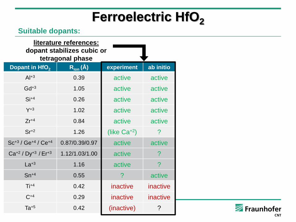
Dopant in HfO2 RIon (Å) experiment ab initio
Al+3 0.39 active active
Gd+3 1.05 active active
Si+4 0.26 active active
Y+3 1.02 active active
Zr+4 0.84 active active
Sr+2 1.26 (like Ca+2) ?
Sc+3 / Ge+4 / Ce+4 0.87/0.39/0.97 active active
Ca+2 / Dy+3 / Er+3 1.12/1.03/1.00 active ?
La+3 1.16 active ?
Sn+4 0.55 ? active
Ti+4 0.42 inactive inactive
C+4 0.29 inactive inactive
Ta+5 0.42 (inactive) ?
literature references:
dopant stabilizes cubic or
tetragonal phase
Ferroelectric HfO2Suitable dopants:

© Fraunhofer
Dopant in HfO2 RIon (Å) experiment ab initio
Al+3 0.39 active active
Gd+3 1.05 active active
Si+4 0.26 active active
Y+3 1.02 active active
Zr+4 0.84 active active
Sr+2 1.26 (like Ca+2) ?
Sc+3 / Ge+4 / Ce+4 0.87/0.39/0.97 active active
Ca+2 / Dy+3 / Er+3 1.12/1.03/1.00 active ?
La+3 1.16 active ?
Sn+4 0.55 ? active
Ti+4 0.42 inactive inactive
C+4 0.29 inactive inactive
Ta+5 0.42 (inactive) ?
literature references:
dopant stabilizes cubic or
tetragonal phase
results from studies:
intemediate FE-Phase
ferroelectricity ALD 3D capability
confirmed +++
confirmed +
confirmed +++
confirmed +
confirmed +++
confirmed +
promising + / +++ / +
promising + / + / +
promising +
promising ++
likely absent ++
absent n/a
likely absent ++
Ferroelectric HfO2Suitable dopants:

© Fraunhofer
3D-integration of FE-HfO2motivation for 3D-integration of FE-HfO2:
high-k Workshop 2014
Jonas Sundqvist
Koyanagi, M. et. al, IEDM (1978)

© Fraunhofer
3D-integration of FE-HfO2motivation for 3D-integration of FE-HfO2:
high-k Workshop 2014
Jonas Sundqvist
Koyanagi, M. et. al, IEDM (1978)
SEM cross section of a
memory-cell array
of 1-Mbit DRAM in trial
production
memory cell measures 4
μm by 8 μm
1st 3D DRAM Capacitor cell at 1Mbit

© Fraunhofer
3D-integration of FE-HfO2Introduction of high-k devices
high-k Workshop 2014
Jonas Sundqvist

© Fraunhofer
McAdams et al., IEEE JSSC, 39,
2004
PZT based FRAM
1 µm
3D-integration of FE-HfO2motivation for 3D-integration of FE-HfO2:
high-k Workshop 2014
Jonas Sundqvist
65 nm, UBM Techinsights
ZrO2 based DRAM
1 µm
Stack capacitor
Current PZT based FRAM
stagnates at 4Mbit Current DRAM´s at 4Gbit
Enabling FRAM to higher storage densities
with 3D FE-HfO2
26 nm, Chipworks
ZrO2 based DRAM
"To continue scaling for more advanced DRAM, Samsung refined its design
and manufacturing technologies and came up with a modified double
patterning and atomic layer deposition. Samsung’s modified double patterning
technology marks a new milestone, by enabling 20nm DDR3 production using
current photolithography equipment and establishing the core technology for
the next generation of 10nm-class DRAM production. Samsung also
successfully created ultrathin dielectric layers of cell capacitors with an
unprecedented uniformity, which has resulted in higher cell performance.“
[Samsung Press Release 18.3.2014]

© Fraunhofer
Source: Globalfoundries Road Map Press ReleaseSource: Koo et al., IEDM 2006
FinFET FinFEFET ? 3D-FRAM (PZT replacement)
? FE-HfO2 ?
3D-integration of FE-HfO2motivation for 3D-integration of FE-HfO2:
high-k Workshop 2014
Jonas Sundqvist
keeping FE-HfO2 based FEFETs compatible to future logic based on
FINFETs requires 3D-capability
the lack of 3D-scaling potential represents one of the major drawbacks of
capacitor-based ferroelectric memories (1T/1C FRAM vs. DRAM)

© Fraunhofer
Koo et al., IEDM (2006)
PZT trench capacitor
- aspect ratio ~ 2:1 -
3D-integration of FE-HfO2conventional ferroelectrics vs. FE-HfO2:
high-k Workshop 2014
Jonas Sundqvist

© Fraunhofer
PZT trench capacitor
- aspect ratio ~ 2:1 -
no FE-phase
achieved
Koo et al., IEDM (2006)
3D-integration of FE-HfO2conventional ferroelectrics vs. FE-HfO2:
high-k Workshop 2014
Jonas Sundqvist

© Fraunhofer
PZT trench capacitor
- aspect ratio ~ 2:1 -
no FE-phase
achieved
our material choice:
ferroelectric Al:HfO2
excellent ALD-precursors for 3-D
step coverage available
reasonable planar Pr values
3D-MIM
vehicle developed at CNT:
Koo et al., IEDM (2006) J. Müller et al., IEDM (2013)
- CNT confidential -
3D-integration of FE-HfO2conventional ferroelectrics vs. FE-HfO2:
high-k Workshop 2014
Jonas Sundqvist

© Fraunhofer
PZT trench capacitor
- aspect ratio ~ 2:1 -
no FE-phase
achieved
FE-HfO2 trench capacitors
- Processflow -
Koo et al., IEDM (2006)
TiN BE+FE-HfO2 TiN TE
Resist+HM RIE etch
Resist+HM Litho 2
SC1 etch Mask removal
- CNT confidential -
J. Müller et al., IEDM (2013)
3D-integration of FE-HfO2conventional ferroelectrics vs. FE-HfO2:
high-k Workshop 2014
Jonas Sundqvist

© Fraunhofer
PZT trench capacitor
- aspect ratio ~ 2:1 -
no FE-phase
achieved
FE-HfO2 trench capacitors
- aspect ratio 13:1 -
FE-phase active
excellent SC of Al:HfO2 achievedKoo et al., IEDM (2006)
- CNT confidential -
J. Müller et al., IEDM (2013)
3D-integration of FE-HfO2conventional ferroelectrics vs. FE-HfO2:
high-k Workshop 2014
Jonas Sundqvist

© Fraunhofer
- CNT confidential -
3D-integration of FE-HfO23D FE-HfO2 electrical data:
high-k Workshop 2014
Jonas Sundqvist
-3 -2 -1 0 1 2 3
-300
-200
-100
0
100
200
300
E-Field [MV/cm]
planar
1k array
3k array
10k array
30k array
100k trench
pola
riz
ati
on
[µ
C/c
m2]
(poje
cte
d a
rea A
*B
)
1k 10k 100k
0
4
8
12
gain
facto
r
trench count
P-E characteristics for different
trench arrays related to the number
of trenches for the projected planar
area
calculated gain factor related to
increase of the capacitor area
Increase of arrays = increase of
projected polarization
maximum gain factor for 100k
arrays of ~10

© Fraunhofer
- CNT confidential -
3D-integration of FE-HfO2
high-k Workshop 2014
Jonas Sundqvist
-3 -2 -1 0 1 2 3
-30
-20
-10
0
10
20
30
E-Field [MV/cm]
planar
1k array
3k array
10k array
30k array
100k array
po
lariz
ati
on
[µ
C/c
m2]
1k 10k 100k
60
80
100n
orm
to
pla
na
r P
r
[%]
trench count
Normalized polarization
(real capacitor area)
relative polarization in relation to
the planar capacitor value
almost same P-E behavior for all
trench arrays stable FE-
Phase for whole trench
3D FE-HfO2 electrical data:

© Fraunhofer
- CNT confidential -
Endurance up to 2*109 cycles for saturated polarization @ 2.5MV/cm
3D-integration of FE-HfO23D FE-HfO2 electrical data:
high-k Workshop 2014
Jonas Sundqvist

© Fraunhofer
FE-HfO2 trench capacitor array
minimal Pr penalty for 3D-integration
- CNT confidential -
J. Müller et al., IEDM (2013)
3D-integration of FE-HfO2Renewed scaling potential:
no significant loss of FE-
Phase stability observed
compared to planar
structures
area gain factor completly
transfered to gain in
polarisation per planar
area-4 -2 0 2 4
-400
-200
0
200
400
electric field (MV/cm)
po
lari
zati
on
(µ
C/c
m2)
(pro
ject
ed a
rea A
*B)
2D vs. 3D
x10
AB
3D
AB
2D
high-k Workshop 2014
Jonas Sundqvist
© Fraunhofer
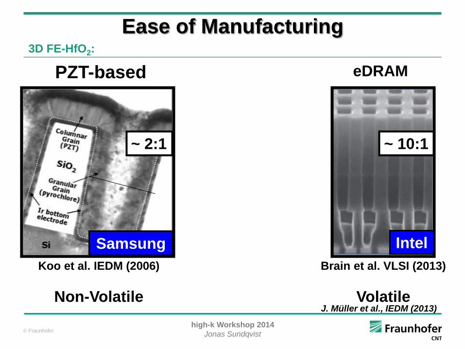
PZT-based eDRAM
~ 10:1~ 2:1
Samsung Intel
Koo et al. IEDM (2006)
Non-Volatile
Brain et al. VLSI (2013)
VolatileJ. Müller et al., IEDM (2013)
Ease of Manufacturing3D FE-HfO2:
high-k Workshop 2014
Jonas Sundqvist

© Fraunhofer
PZT-based FE-HfO2 eDRAM
our work
Non-Volatile
~ 10:113:1~ 2:1
Samsung Intel
Koo et al. IEDM (2006)
Non-Volatile
Brain et al. VLSI (2013)
VolatileJ. Müller et al., IEDM (2013)
Ease of Manufacturing3D FE-HfO2:
high-k Workshop 2014
Jonas Sundqvist

© Fraunhofer
PZT-based FE-HfO2 eDRAM
our work
~ 10:113:1~ 2:1
J. Müller et al., IEDM (2013)
Samsung Intel
Koo et al. IEDM (2006) Brain et al. VLSI (2013)
Possibility to scale FRAM with DRAM
Ease of Manufacturing3D FE-HfO2:
high-k Workshop 2014
Jonas Sundqvist

© Fraunhofer
Gate First
Ease of ManufacturingFeFET as Embedded Memory Solution for HKMG:
high-k Workshop 2014
Jonas Sundqvist
SiO2
silicon
2D Fe-HfO2
metal electrode
fill metal

© Fraunhofer
Gate First Gate Last
Ease of ManufacturingFeFET as Embedded Memory Solution for HKMG:
high-k Workshop 2014
Jonas Sundqvist
SiO2
silicon
3D Fe-HfO2
metal electrode
fill metal
SiO2
silicon
2D Fe-HfO2
metal electrode
fill metal

© Fraunhofer
Gate First Gate Last FinFET
Ease of ManufacturingFeFET as Embedded Memory Solution for HKMG:
high-k Workshop 2014
Jonas Sundqvist
SiO2
silicon
3D Fe-HfO2
metal electrode
fill metal
SiO2
silicon
2D Fe-HfO2
metal electrode
fill metal
SiO2
silicon
3D Fe-HfO2
metal electrode
fill metal

© Fraunhofer
Gate First Gate Last FinFET
Ease of ManufacturingFeFET as Embedded Memory Solution for HKMG:
high-k Workshop 2014
Jonas Sundqvist
SiO2
silicon
3D Fe-HfO2
metal electrode
fill metal
SiO2
silicon
2D Fe-HfO2
metal electrode
fill metal
SiO2
silicon
3D Fe-HfO2
metal electrode
fill metal

© Fraunhofer
Conclusions
FE-HfO2 ALD is 3D capable and scalable with DRAM and eDRAM
technology
Embedded FRAM for integration in BEOL, <400°C Thermal budget proven
Embedded FEFETs in FEOL
High-k first planar : proven
Replacement Gate 3D : ongoing
FinFET : demonstration needed
high-k Workshop 2014
Jonas Sundqvist

© Fraunhofer
… and for funding to:
For your attention …
…K. Biedermann, J. Paul and our eBeam Team…

© Fraunhofer
… please feel
free to ask…
high-k Workshop 2014
Jonas Sundqvist

© Fraunhofer high-k Workshop 2014
Jonas Sundqvist
Intel’s e-DRAM Shows Up In The Wild
http://electroiq.com/chipworks_real_chips_blog/2014/02
/07/intels-e-dram-shows-up-in-the-wild/
When Intel launched their Haswell series chips last
June, they stated that the high-end systems would have
embedded DRAM, as a separate chip in the package;
and they gave a paper at the VLSI Technology
Symposium [1] that month, and another at IEDM [2].

© Fraunhofer high-k Workshop 2014
Jonas Sundqvist