power conditioning unit for a harvester circuit · power conditioning unit for a harvester circuit...
TRANSCRIPT

Power Conditioning Unit for a Harvester Circuit
Diogo Goncalves Barroso da Silva Santos
Thesis to obtain the Master of Science Degree in
Electrical and Computer Engineering
Supervisors: Prof. Dr. Jorge Manuel dos Santos Ribeiro Fernandes
MSc. Hugo Miguel Barreto Goncalves
Examination CommitteeChairperson: Prof. Dr. Goncalo Nuno Gomes Tavares
Supervisor: Prof. Dr. Jorge Manuel dos Santos Ribeiro FernandesMember of the Committee: Prof. Dr. Nuno Filipe Paulino
November 2016


Acknowledgments
I would like to start by thanking my supervisor Prof. Jorge Fernandes and co-supervisor MSc.
Hugo Goncalves for the opportunity to work in this research field. Their guidance and availability
were fundamental to this work.
Throughout the period of this thesis I had the privilege to work with the researchers of GCAM
(Grupo de Circuitos Analogicos e Mistos), whose support and sympathy cannot be forgotten. I
owe a deep sense of gratitude to Fabio Rabuske for his priceless contributions.
Once this is the final step of a long walk on the Tecnico Campus, I have to acknowledge the
friends I have made through it. I especially wish to thank Hugo Silva for his help on the thesis
revision, Francisco Rosario for his advices and Joao Ventura for being my partner in almost every
class. I would also like to thank my long time friends: Miguel Dias, Andre Caetano and Ricardo
Simoes.
Finally I have to thank my family for all their support and encouragement: Alexandrina Barroso,
Alice Silva, Anibal Silva, Cristina Santos, Nuno Santos and Pedro Santos.


Abstract
This work presents a Power Conditioning Unit (PCU) for autonomously powered devices. Au-
tonomously powered devices are passive systems and require an harvester circuit followed by
a PCU to manage the power delivered to a load circuit. These systems assume a relevant role
in the design of biomedical implants and wireless sensor networks. As different energy sources
are accountable (sunlight, vibrations, RF) and its power is dependent on external conditions, it is
important that the passive systems are tolerant to the harvested power variability. For this reason,
the proposed PCU applies an intermittent load activation control and a power limiting functionality.
Furthermore, it has to have a negligible idle power dissipation, when compared to the low power
output provided by state-of-the-art harvesters (< 1 µW). The PCU uses a voltage sensor with hys-
teresis and a voltage limiter to control the load activation and define the maximum voltage. The
load activation and deactivation voltages, and maximum voltage are known as transition voltages.
Both blocks are based on a low voltage circuit composed by a pico-watt reference and a CMOS
inverter, providing a voltage sensing, while imposing a maximum steady state current equal to
2 nA. The PCU is designed in a 130 nm process at simulation level and is able to control the
transition voltages with a ±10 % precision on a −25 oC to 90 oC range.
Keywords
Energy Harvesting, Voltage Sensor, Voltage Limiter, Low Power, Temperature Compensation
iii


Resumo
Este trabalho apresenta uma Unidade de Condicionamento de Potencia (UCP) para dispos-
itivos autonomamente alimentados. Estes dispositivos sao sistemas passivos e requerem um
circuito recolector seguido de uma UCP para gerir a potencia entregue a um circuito de carga.
Estes sistemas sao usados para o desenvolvimento de redes de sensores sem fios e implantes
biomedicos. Uma vez que diferentes fontes de energia podem ser usadas (luz solar, vibracoes,
RF) e a sua potencia depende das condicoes exteriores, e importante que os sistemas passivos
seja tolerantes a variabilidade da potencia recolhida. Por este motivo, a UCP proposta permite
que a carga seja activada intermitentemente e limita a potencia entregue a esta dissipando uma
potencia insignificante, quando comparada com a baixa potencia disponibilizada pelos recolec-
tores no estado da arte (< 1 µW). A UCP usa um sensor de tensao com histerese e um limitador
de tensao para controlar a activacao da carga e definir a tensao maxima do sistema passivo. A
tensao onde a carga e activada ou desactivada, e a tensao maxima sao identificadas como as
tensoes de transicao. Ambos os blocos baseiam-se num circuito de baixa tensao composto por
um inversor CMOS e uma referencia de muito baixa potencia. Este permite detectar a tensao
enquanto apenas requer uma corrente de 2 nA. A UCP e desenvolvida a nıvel de simulacao num
processo de 130 nm e controla as tensoes de transicao do circuito de carga com uma precisao
de ±10 % numa gama de −25 oC a 90 oC.
Palavras Chave
Recolha de Energia, Sensor de Tensao, Limitador de Tensao, Baixa Potencia, Compensacao
de Temperatura
v


Contents
1 Introduction 1
1.1 Motivation . . . . . . . . . . . . . . . . . . . . . . . . . . . . . . . . . . . . . . . . . 2
1.2 Research Goals and Structure . . . . . . . . . . . . . . . . . . . . . . . . . . . . . 4
1.3 Original Contributions . . . . . . . . . . . . . . . . . . . . . . . . . . . . . . . . . . 5
2 Power Conditioning 7
2.1 Overview . . . . . . . . . . . . . . . . . . . . . . . . . . . . . . . . . . . . . . . . . 8
2.1.1 Energy Harvester . . . . . . . . . . . . . . . . . . . . . . . . . . . . . . . . 8
2.1.2 Power Conditioning Unit . . . . . . . . . . . . . . . . . . . . . . . . . . . . . 9
2.1.3 Load Circuit . . . . . . . . . . . . . . . . . . . . . . . . . . . . . . . . . . . . 10
2.2 System Operation . . . . . . . . . . . . . . . . . . . . . . . . . . . . . . . . . . . . 10
2.3 PCUs: Blocks and Structure . . . . . . . . . . . . . . . . . . . . . . . . . . . . . . . 11
2.3.1 Voltage Sensors . . . . . . . . . . . . . . . . . . . . . . . . . . . . . . . . . 12
2.3.2 Voltage Limiters . . . . . . . . . . . . . . . . . . . . . . . . . . . . . . . . . 14
2.3.3 State-of-the-art analysis . . . . . . . . . . . . . . . . . . . . . . . . . . . . . 15
3 PCU Circuits 17
3.1 MOS transistors review . . . . . . . . . . . . . . . . . . . . . . . . . . . . . . . . . 18
3.2 Comparator Circuits . . . . . . . . . . . . . . . . . . . . . . . . . . . . . . . . . . . 19
3.3 Voltage References . . . . . . . . . . . . . . . . . . . . . . . . . . . . . . . . . . . 22
4 Proposed PCU: Circuit Design and Results 25
4.1 Solution Overview . . . . . . . . . . . . . . . . . . . . . . . . . . . . . . . . . . . . 26
4.1.1 Structure . . . . . . . . . . . . . . . . . . . . . . . . . . . . . . . . . . . . . 26
4.1.2 Design Considerations . . . . . . . . . . . . . . . . . . . . . . . . . . . . . . 27
4.2 Voltage Sensor . . . . . . . . . . . . . . . . . . . . . . . . . . . . . . . . . . . . . . 28
4.2.1 Voltage Sensing Core . . . . . . . . . . . . . . . . . . . . . . . . . . . . . . 29
4.2.2 Voltage Conversion . . . . . . . . . . . . . . . . . . . . . . . . . . . . . . . 32
4.2.3 Temperature Compensation . . . . . . . . . . . . . . . . . . . . . . . . . . . 37
4.2.4 Complete Block . . . . . . . . . . . . . . . . . . . . . . . . . . . . . . . . . . 41
vii

4.3 Voltage Limiter . . . . . . . . . . . . . . . . . . . . . . . . . . . . . . . . . . . . . . 45
4.3.1 Circuit Discharge and Temperature Compensation . . . . . . . . . . . . . . 45
4.3.2 Complete Block . . . . . . . . . . . . . . . . . . . . . . . . . . . . . . . . . . 48
4.4 Final PCU . . . . . . . . . . . . . . . . . . . . . . . . . . . . . . . . . . . . . . . . . 49
4.4.1 Combined Blocks Evaluation . . . . . . . . . . . . . . . . . . . . . . . . . . 49
4.4.2 Layout and Results . . . . . . . . . . . . . . . . . . . . . . . . . . . . . . . . 51
4.4.3 Discussion . . . . . . . . . . . . . . . . . . . . . . . . . . . . . . . . . . . . 55
5 Conclusions 59
5.1 Work Conclusions . . . . . . . . . . . . . . . . . . . . . . . . . . . . . . . . . . . . 60
5.2 Future Work . . . . . . . . . . . . . . . . . . . . . . . . . . . . . . . . . . . . . . . . 61
A Passive System Supply 67
B Final Corners Data 70
viii
List of Figures
1.1 Interior of a Smart Card transportation ticket [12]. . . . . . . . . . . . . . . . . . . . 3
1.2 Structure and energy flow of the passive system. . . . . . . . . . . . . . . . . . . . 3
2.1 RF passive system structure. . . . . . . . . . . . . . . . . . . . . . . . . . . . . . . 8
2.2 Proposed high level model of the passive system. . . . . . . . . . . . . . . . . . . 8
2.3 Variation of the passive system supply voltage (VDC) through time for an intermit-
tent operation. . . . . . . . . . . . . . . . . . . . . . . . . . . . . . . . . . . . . . . 10
2.4 Passive system supply voltage (VDC) for the (a) continuous and (b) voltage limiting
operations. . . . . . . . . . . . . . . . . . . . . . . . . . . . . . . . . . . . . . . . . 11
2.5 State-of-the-art PCU structure composed by a voltage sensor, a limiter and a reg-
ulator that outputs the load voltage supply VLoad. . . . . . . . . . . . . . . . . . . . 12
2.6 (a) Typical structure of the voltage sensor block. (b) Plot of the sensed voltage VS
and sensor output VO for the supply VDC . . . . . . . . . . . . . . . . . . . . . . . . 12
2.7 (a) Schematic of a voltage sensor with hysteresis behaviour. (b) Plot of the sensed
voltages VS resultant of the division ratios α0 and α1, and the corresponding sensor
output VO characteristic. . . . . . . . . . . . . . . . . . . . . . . . . . . . . . . . . . 13
2.8 (a) Voltage sensor with hysteresis using a comparator with offset VOS and no ref-
erence circuits. (b) Plot of the voltage sensed VS , and corresponding output of the
sensor circuit VO. . . . . . . . . . . . . . . . . . . . . . . . . . . . . . . . . . . . . . 14
2.9 (a) Voltage limiter based on several diodes in series. (b) Voltage limiter based
on a voltage sensor and MOS transistor. (c) Plot of the voltage sensed VS , and
corresponding output of the sensor circuit VO in the voltage limiter of (b). . . . . . . 15
3.1 Comparators schematic. (a) A (Pseudo) Differential Pair. (b) A CMOS Inverter. . . 20
3.2 (a) BJT based reference circuit. (b) 2T reference circuit. . . . . . . . . . . . . . . . 22
4.1 Proposed Power Conditioning Unit (PCU) circuit blocks structure. . . . . . . . . . . 26
4.2 Passive system testbench used for the PCU simulation. . . . . . . . . . . . . . . . 27
4.3 Proposed voltage sensor circuit structure. . . . . . . . . . . . . . . . . . . . . . . . 29
4.4 High level and transistor view of the voltage sensing core. . . . . . . . . . . . . . . 30
ix

4.5 Reference voltage VREF characteristic for VS . . . . . . . . . . . . . . . . . . . . . . 31
4.6 Voltage sensing core output VO and inverter current IC characteristics. . . . . . . . 31
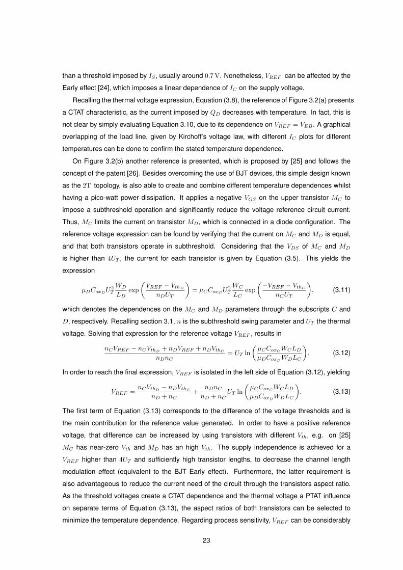
4.7 Voltage sensor with voltage divider made with ideal resistors. . . . . . . . . . . . . 32
4.8 Passive system supply VDC , sensed voltage VS and voltage sensor current IV S for
an intermittent system operation with IS = 1 µA and RL = 0.3 MΩ. . . . . . . . . . 34
4.9 Zoom of the VON transition with an emphasis on the ILV L, VO, P EN , VS and VO
signals. . . . . . . . . . . . . . . . . . . . . . . . . . . . . . . . . . . . . . . . . . . 34
4.10 Zoom of the VOFF transition with an emphasis on the ILV L, VO, P EN , VS and
VO signals. . . . . . . . . . . . . . . . . . . . . . . . . . . . . . . . . . . . . . . . . 35
4.11 Focus on the voltage divider and low voltage circuit when RD is eliminated. . . . . 36
4.12 Zoom of the VON transition with an emphasis on the ILV , VO, VS and VO signals
when the voltage divider has hysteresis and resistor RD= 1 TΩ. . . . . . . . . . . 36
4.13 Temperature influence on VREF , VTS for a temperature stable VREF= 0.1 V and
VTS real. . . . . . . . . . . . . . . . . . . . . . . . . . . . . . . . . . . . . . . . . . 37
4.14 Temperature influence on RTS and VTS before and after the level shifter application. 38
4.15 (a)Voltage divider with PMOS. (b)Voltage divider based on PMOS string. . . . . . . 39
4.16 (a)Final voltage sensor circuit schematic.(b)Aspect ratios applied on the final volt-
age sensor transistors. . . . . . . . . . . . . . . . . . . . . . . . . . . . . . . . . . . 40
4.17 (a)VON , (b)VOFF , (c)Pav and Ip for the −40 to 100 oC temperature range. . . . . . 41
4.18 Monte Carlo simulation results for (a)Pav and (b) Ip. . . . . . . . . . . . . . . . . . 42
4.19 Monte Carlo simulation results for (a)VONand (b)VOFF . . . . . . . . . . . . . . . . 43
4.20 Voltage limiter structure when active. P EN powers down the limiter when high. . 45
4.21 (a) Proposed voltage limiter circuit schematic. (b) Aspect ratios of the transistors in
the schematic. . . . . . . . . . . . . . . . . . . . . . . . . . . . . . . . . . . . . . . 46
4.22 Voltage limiter transient response for RL = 0.3 MΩ, (a) IS = 10 µA and (b) IS =
20 µA. . . . . . . . . . . . . . . . . . . . . . . . . . . . . . . . . . . . . . . . . . . . 47
4.23 (a) VLim transition and final VDC voltages for the temperature range after the tem-
perature compensation is applied. (b) Voltage limiter transient response for IS = 20
µA and RL = 0.3 MΩ after applying the MOS string. . . . . . . . . . . . . . . . . 48
4.24 PCU simulation for IS= 10 µA during 0.1 s and IS= 1 µA afterwards. . . . . . . . 50
4.25 Layout implementation of the proposed PCU. . . . . . . . . . . . . . . . . . . . . . 52
4.26 Layout implementation of the proposed PCU with pads. . . . . . . . . . . . . . . . 53
A.1 (a) Circuit schematic when the load is active. (b) Circuit schematic when the load
is inactive. . . . . . . . . . . . . . . . . . . . . . . . . . . . . . . . . . . . . . . . . . 68
B.1 Average power variation for Metal Oxide Semiconductor (MOS) process corners
and temperature range. . . . . . . . . . . . . . . . . . . . . . . . . . . . . . . . . . 71
x

B.2 Variation of load activation voltage for MOS process corners and temperature range. 71
B.3 Variation of load deactivation voltage for MOS process corners and temperature
range. . . . . . . . . . . . . . . . . . . . . . . . . . . . . . . . . . . . . . . . . . . . 72
B.4 Variation of current spike value for MOS process corners and temperature range. . 72
B.5 Variation of limiting voltage for MOS process corners and temperature range. . . . 72
xi

xii

List of Tables
1.1 State-of-the-art harvesters comparison. . . . . . . . . . . . . . . . . . . . . . . . . 2
1.2 Specifications summary. . . . . . . . . . . . . . . . . . . . . . . . . . . . . . . . . . 4
2.1 State-of-the-art PCUs comparison. . . . . . . . . . . . . . . . . . . . . . . . . . . . 16
2.2 Relative transition voltage tolerance and current required by state-of-the-art voltage
sensors. . . . . . . . . . . . . . . . . . . . . . . . . . . . . . . . . . . . . . . . . . . 16
3.1 Differential pair average power for different reference voltages. To minimize the
dissipated power the aspect ratios 0.16µm/1.5µm and 0.16µm/7µm are used on
the N-type MOS (NMOS) and P-type MOS (PMOS) transistors, respectively. . . . . 21
3.2 CMOS inverter average power for different input voltages. The NMOS and PMOS
transistors aspect ratios are equal to 0.16µm/10µm. . . . . . . . . . . . . . . . . . 21
4.1 Nominal and acceptable voltage transition interval for the three required voltage
transitions. . . . . . . . . . . . . . . . . . . . . . . . . . . . . . . . . . . . . . . . . 28
4.2 Minimum charge and active time analysis for nominal temperature. . . . . . . . . . 42
4.3 Monte Carlo yield analysis for different number of runs and temperature ranges. . 43
4.4 Process corner and industrial temperature range influence on the VON , VOFF and
VTS transition voltages mean µ and variation ±∆. . . . . . . . . . . . . . . . . . . 44
4.5 Process corner and industrial temperature range influence on the maximum VREF
and VTS for a temperature stable VREF= 0.1 V. Results detailed in the form of
mean µ and variation ±∆. . . . . . . . . . . . . . . . . . . . . . . . . . . . . . . . . 44
4.6 Process corner and temperature range (−40 oC to 100 oC) influence on the final
VDC and VLim voltages mean µ and variation ∆. . . . . . . . . . . . . . . . . . . . 49
4.7 Voltage sensor and limiter specifications obtained for the separate and combined
circuits tests. . . . . . . . . . . . . . . . . . . . . . . . . . . . . . . . . . . . . . . . 49
4.8 Yield analysis of the Monte Carlo results for the final PCU when testing the inter-
mittent operation. . . . . . . . . . . . . . . . . . . . . . . . . . . . . . . . . . . . . . 50
4.9 Yield analysis of the Monte Carlo results for the final PCU when testing the voltage
limiting operation. . . . . . . . . . . . . . . . . . . . . . . . . . . . . . . . . . . . . . 51
xiii

4.10 Comparison of the pre and post-layout simulation results for the intermittent and
voltage limiting modes on the nominal temperature. . . . . . . . . . . . . . . . . . . 54
4.11 Voltage sensor and limiter minimum time specifications obtained for the pre and
post-layout simulations on nominal temperature. . . . . . . . . . . . . . . . . . . . 54
4.12 Comparison of the yields obtained for pre and post layout on the −25 oC to 90 oC
range. The mean (µ), the total (∆) and the 3σ variations are reported for each
specification. . . . . . . . . . . . . . . . . . . . . . . . . . . . . . . . . . . . . . . . 54
4.13 Results obtained for post-layout simulations on MOS process corners and −25 oC
to 90 oC range. . . . . . . . . . . . . . . . . . . . . . . . . . . . . . . . . . . . . . . 55
4.14 Comparison of the PCU specifications. . . . . . . . . . . . . . . . . . . . . . . . . . 56
4.15 Comparison of the transition voltage precision for temperature and corners. . . . . 56
4.16 Comparison of the specifications achieved by Monte Carlo analysis and the targets
proposed in the research goals. . . . . . . . . . . . . . . . . . . . . . . . . . . . . . 57
5.1 Final PCU specifications summary. . . . . . . . . . . . . . . . . . . . . . . . . . . . 61
xiv

List of Acronyms
AC Alternating Current
BJT Bipolar Junction Transistor
BO Brown-Out
DC Direct Current
CTAT Complementary To Absolute Temperature
CMOS Complementary MOS
FF Fast-N Fast-P
FNSP Fast-N Slow-P
IC Integrated Circuit
LVI Low Voltage Inverter of the level shifter block
MOS Metal Oxide Semiconductor
MOSFET Metal Oxide Semiconductor Field Effect Transistor
NMOS N-type MOS
PCE Power Conversion Efficiency
PCU Power Conditioning Unit
PMOS P-type MOS
POR Power-On Reset
PTAT Proportional To Absolute Temperature
PVT Process, Voltage and Temperature
RC Resistor-Capacitor
RF Radio Frequency
xv

RFID Radio Frequency Identification
SS Slow-N Slow-P
SNFP Slow-N Fast-P
TC Temperature Coefficient
UMC United Microelectronics Corporation
WSN Wireless Sensor Network
xvi

Nomenclature
COut Harvester output capacitor.
Cox Oxide capacitance.
IC Current of the inverter in the voltage sensing core.
IS Ideal harvester current output.
ILV L Level shifter main block current.
ILV Current on the low voltage circuit.
IPCU PCU current.
IV L Voltage Limiter current.
IV S Voltage sensor current.
Idisc Discharge current.
Ip Peak current.
L Transistors length.
NU Number of transistors in the MOS string.
Pav Average power dissipated.
RD Voltage divider down resistor.
RU Voltage divider up resistor.
RLV Low voltage circuit equivalent resistance.
RL Load circuit resistance.
RPCU PCU equivalent resistance.
RTS RLV at the voltage sensing core transition.
RU0 Voltage sensor up resistor when the load is inactive.
xvii

RU1 Voltage sensor up resistor when the load is active.
RUL Voltage limiter up resistor.
T Temperature.
Tr Reference temperature.
UT Thermal voltage.
VO Voltage sensing core output signal
VS Sensed voltage.
VDC Harvester output voltage.
VDS Drain-to-source voltage.
VGS Gate-to-source voltage.
VLim Maximum allowable voltage supply value.
VLoad Load circuit supply voltage.
VOFF Load deactivation transition voltage.
VON Load activation transition voltage.
VOS Sensor offset voltage.
VREF Reference voltage.
VTR Transition voltage of the voltage sensor output.
VTS Transition voltage of the voltage sensing core output.
Vdisc Discharge control voltage.
Vth Threshold voltage.
W Transistors width.
∆tL Time period between the load and limiting activations.
∆tON Load circuit active time period.
α Division ratio.
α0 Inactive load division constant.
α1 Active load division constant.
xviii

αL Voltage limiting division constant.
µ Charge-carrier effective mobility.
P EN Complementary power enable signal
VO Output voltage of the level shifter low voltage inverter.
k Boltzmann constant.
n Subthreshold swing parameter.
q Electron charge.
t0 Start-up time.
P EN Power enable signal
xix

xx

1Introduction
Contents1.1 Motivation . . . . . . . . . . . . . . . . . . . . . . . . . . . . . . . . . . . . . . . 21.2 Research Goals and Structure . . . . . . . . . . . . . . . . . . . . . . . . . . . . 41.3 Original Contributions . . . . . . . . . . . . . . . . . . . . . . . . . . . . . . . . 5
1

This chapter defines the purpose of conditioning the power provided by harvester circuits.
To do it, the harvesters specifications are introduced and the Power Conditioning Units (PCUs)
functions are detailed. The main goals of this work are presented and the summary of the following
chapters is stated. Furthermore, the contributions of this work are provided.
1.1 Motivation
Wireless power transmission is a relevant research field for its role on the development of
autonomously powered devices. These correspond to electrical devices that only require the
energy provided by harvesting to operate. Due to this characteristic, such systems can be applied
in remote locations or difficult access places. The circuit responsible for providing the energy
to the system is known as energy harvester. Nowadays, the temperature gradients, vibrations,
sunlight, and Radio Frequency (RF) waves are some of the accountable external sources that
can be harvested.
The combination of an harvester and a load circuit is known as passive system. In order to
store the harvested energy, usually a capacitor is used at the harvester output. Considering previ-
ous studies [1], it is verified that the RF harvesters provide less power than any of those previously
mentioned. To verify the power input required to provide a certain power output, the sensitivity
and Power Conversion Efficiency (PCE) of the state-of-the-art RF harvesters are presented in
Table 1.1. By its analysis it can be verified that the minimum input power is −20 dBm (10 µW).
That input allows the operation of 1 MΩ load at 1 V, which corresponds to 1 µW. Considering the
previous facts, a major focus is given to the RF harvesters.
Table 1.1: State-of-the-art harvesters comparison.Reference [2] [3] [4] [5]
PCE 13.2 % 5.1 % 7.7 % 10 %
Sensitivityand Load
−11.12 dBm1 V
200 kΩ
−14.1 dBm1 V
0.5 MΩ
−17.27 dBm1.2 V1 MΩ
−20 dBm1 V
1 MΩ
Commonly RF harvesters are used to supply low power circuits, such as front-end interfaces,
memory cells and sensors. The Radio Frequency Identification (RFID) systems [6–8] are one of
the examples, which are used for shopping tags and Smart Card transportation tickets, Figure
1.1. Other applications are Wireless Sensor Networks (WSNs) [9], which can be applied in very
different scenarios, as for forest surveillance, for biomedical implants [10,11], etc.
As stated by the Friis formula, the power that arrives to the RF based passive system, depends
on its distance from the RF source. Therefore, the power provided by the harvester presents an
undesired variability to the load. To counter this problem, Power Conditioning Units (PCUs) are
applied in the passive system between the energy harvester and the load circuit, Figure 1.2. In
order for the circuit to operate correctly and not be damaged, a PCU stabilizes and limits power
2
Figure 1.1: Interior of a Smart Card transportation ticket [12].
delivered to the load. Moreover, it controls the activation of the load circuit. This last characteristic
is a key function for low power harvesters, once that it allows the passive system to operate
intermittently. When an intermittent operation is applied, the passive system is based on charge
and discharge cycles [9]. Hence, on the charge phase, the system harvests the energy and stores
it in the capacitor. When the capacitor charge is sufficiently high to deliver the power required by
the load, the system is discharged.
The state-of-the-art PCUs are based on three functions: stored energy evaluation, load ac-
tivation and power delivery. The energy evaluation function, corresponds to the sensing of the
voltage at the capacitor terminals. Depending on that voltage, the load is activated or deactivated.
Finally, when the load is activated, the power delivered to the load has to be regulated and lim-
ited. Therefore, the circuit blocks used to implement such functions are voltage sensors, voltage
regulators and voltage limiters.
Figure 1.2: Structure and energy flow of the passive system.
In order for the system to be power efficient, the power required by the PCU has to be lower
than the provided by the harvester. Consequently, the circuit blocks applied in the PCU must have
a power dissipation below the 1 µW provided by the state-of-the-art RF harvesters.
3

1.2 Research Goals and Structure
This work proposes the development of a PCU that delivers the energy gathered from any
kind of harvester to a generic load. As stated before, a major focus is given to RF, nonetheless
the assumed PCU design considerations can be applied to other types of energy harvesters.
Based on state-of-the-art results [4, 5], it is imposed that the harvester is able to provide a 1 µA
output current. For design purposes, a 50 nF storage capacitor is used as storage and the load
is characterized as a resistance. The prototype circuit is developed in a standard 130 nm (UMC)
process.
An intermittent operation approach is used on the PCU design. It is considered that the sys-
tem has gathered enough energy to power the load when the supply reaches 1.2 V. When the
supply decreases to 0.4 V the load is deactivated. The PCU to be developed must also limit the
voltage that is delivered to the load, to insure that overvoltage does not occur. That is considered
to happen when the harvested supply reaches 1.5 V. The load activation (1.2 V), deactivation
(0.4 V) and maximum (1.5 V) voltages are defined as the transition voltages. Based on these
requirements, the proposed PCU has to contain a voltage sensor and voltage limiter. Once the
PCU current is limited to the provided by the harvester, the possible spikes in the PCU current
cannot surpass the current provided by the harvester. Although a voltage regulation is critical for a
correct load operation, the implementation of this feature is not included in this work. To optimize
the system power efficiency, a constraint on the PCU power dissipation of 10 nW is imposed.
The circuit has to be tolerant to the variation of the Process, Voltage and Temperature (PVT) con-
ditions. Hence, a ±10% precision tolerance is imposed for the transition voltages considering a
temperature range from −40 oC to 100 oC and fabrication process corners. To reduce the cost,
only high speed transistors are used. The specifications summary is provided in Table 1.2.
Table 1.2: Specifications summary.Load
Activation Voltage 1.2 V
LoadDeactivation Voltage 0.4 V
LimitVoltage 1.5 V
Power 10 nWPeak
Current 1 µA
Transition VoltagesTolerance ±10 %
Temperature [−40 100] oC
The following chapters of this document present the PCU prototype development, starting from
the state-of-the-art review until the layout implementation and statement of the final conclusions.
The chapters structure and summary is:
4

Chapter 2 Introduces the passive system structure and based on a ideal model describes its
expected behaviour relatively to the generated voltage supply. A state-of-the-art review is
done, illustrating the common PCU structure, blocks and results.
Chapter 3 Proposes a review at transistor level on the commonly used circuits in the PCU lit-
erature. Their operation, power dissipation and temperature performance are discussed in
order to elaborate a circuit that matches the required research goals.
Chapter 4 The complete design procedure from the high level circuit structure to the layout im-
plementation of the voltage sensor and limiter blocks is done. Along this process, the blocks
are evaluated based on nominal and PVT simulations.
Chapter 5 Provides the final considerations on the developed PCU, comparing the results ob-
tained to those proposed. Furthermore, states the following steps for the continuation of this
work.
1.3 Original Contributions
As an initial iteration of this work, the author cooperated with Hugo Goncalves and Fabio
Rabuske in the design of a PCU prototype at simulation level. This led to the publishing of a
paper [13] in the 2016 PRIME conference. That circuit combines two voltage sensors and a
voltage limiter to achieve a temperature tolerance of ±7.5 % on the transition voltages precision
from −25 oC to 125 oC. Furthermore it only requires 4 nW to operate.
A voltage sensor and a voltage limiter are designed with a circuit topology different from the
differential pair, which is the most used in the PCU literature. The current required by the proposed
circuits is lower than the achieved in the state-of-the-art.
A temperature compensation method based on resistors made with a string of diode con-
nected Metal Oxide Semiconductor (MOS) transistors is proposed. The influence of the number
of transistors and dimensions applied is detailed. Based on this method, the achieved temperature
tolerance is ±10 % with a yield of 88 %.
5

6

2Power Conditioning
Contents2.1 Overview . . . . . . . . . . . . . . . . . . . . . . . . . . . . . . . . . . . . . . . . 82.2 System Operation . . . . . . . . . . . . . . . . . . . . . . . . . . . . . . . . . . . 102.3 PCUs: Blocks and Structure . . . . . . . . . . . . . . . . . . . . . . . . . . . . . 11
7

The main purpose of this chapter is to verify the power conditioning role on passive systems.
In order to do it, firstly the passive systems structure and operation are defined. Then, the PCUs
internal blocks are generically characterized and the state-of-the-art results are presented.
2.1 Overview
To understand a passive system operation, the influence of each of the blocks on the power
delivering process to the load circuit has to be verified. Figure 2.1 illustrates the internal structure
of an RF passive system, which is characterized by three blocks: the energy harvester, the PCU
and the load circuit. The harvester is represented as an antenna and an energy harvesting circuit.
Figure 2.1: RF passive system structure.
Figure 2.2 presents an equivalent high level model of the circuit blocks presented in Figure 2.1.
The harvester and load circuits are replaced by ideal electrical components, whereas the PCU is
defined as a circuit block that outputs VLoad based on the supply VDC . The analysis performed
in this chapter considers a complete PCU, which includes all the conditioning features: voltage
sensing, limiting and regulation. The following subsections establish the link between the circuits
of Figures 2.1 and 2.2.
Figure 2.2: Proposed high level model of the passive system.
2.1.1 Energy Harvester
The energy harvester provides the voltage supply VDC for the other circuit blocks and con-
sists in two parts: the energy transducer and the harvester circuit. Considering RF energy, the
8

transducer is the referred antenna, and the circuit is composed by a matching network and a rec-
tifier, as presented in Figure 2.1. The matching network maximizes the power transfer from the
antenna to the rectifier and the rectifier converts the Alternating Current (AC) signal into Direct
Current (DC). The relation between the antenna input power and the rectifier output is defined as
the PCE.
In the schematic of Figure 2.2, the energy harvesting block is composed by a current source IS
and a capacitor COut. The current source value correlates to the power that the harvester is able
to provide to a circuit. This is an adaptation of the lossless model proposed by [14], using Norton’s
theorem. In fact, the PCE not only depends on the input power, but also on the loading condition,
which is the impedance ”seen” from the current source output. Nonetheless, it is important to
define a maximum and minimum IS . The minimum is ensured by the harvester sensitivity and
loading conditions shown in Table 1.1. Using the harvester proposed in [5], the value for IS is
approximately 1 µA. The energy harvester does not impose a maximum IS value and for the
analysis made in this thesis it is not relevant.
2.1.2 Power Conditioning Unit
The conditioning unit can be interpreted as a gate that establishes the power link between the
harvester and the load. Recalling section 1.1, to fully accomplish that role, the conditioning unit
is responsible for three different functions: stored energy evaluation, load activation and power
delivery.
Regarding the first conditioning function, the energy stored in a capacitor is directly related to
the voltage at its terminals. In a passive system, the capacitor is connected to the harvester output
VDC , therefore it is required that the PCU performs a voltage sensing. By doing this function, the
load can be activated based on the VDC value. The activation occurs for VDC = VON , which
turns ON the PCU block output of Figure 2.2, by outputting a positive and constant VLoad. The
deactivation is set by VDC = VOFF and makes VLoad a high impedance node. In order to ensure
a more robust PCU response to sudden VDC variations [8], an hysteresis behaviour is applied.
The power delivery occurs when the load is active. This last PCU function is divided in two
parts: voltage regulation and limiting. Circuits require a stable voltage supply to operate. To imple-
ment it, the PCU circuits apply feedback techniques to make the voltage given to the load circuit
as independent as possible of the harvester output voltage. This ability is known as line regula-
tion. Besides that, a load regulation is also imposed, consisting in the capability of the PCU to
maintain a specific voltage given load variations. The voltage limiting consists in imposing a max-
imum VDC value VLim, so that the passive system integrity can be ensured when the harvester
provides excessive power to the system. On that event, the PCU activates a low impedance path
where the excessive power is dissipated, thereby limiting VDC .
9
2.1.3 Load Circuit
The loads commonly applied in the passive system literature are memory circuits [6, 8] or
transmitter units, connected to control logic [9, 15] and eventually memory elements [7]. For the
PCU design point of view, that circuit block can be interpreted as a resistor RL (Figure 2.2) with
voltage and operating time requirements.
2.2 System Operation
The system previously described by Figure 2.2, allows the load to operate intermittently or
continuously depending on the power harvested and the power required by the system, which
corresponds to the power delivered to the PCU and load circuit. When the harvested power
is below the required power, the load can only operate intermittently, once it relies on the energy
stored in COut. The voltage VDC behaves as presented in Figure 2.3 for an intermittent operation.
The time t0 corresponds to the start-up time, which is the time required for the discharged passive
system to reach VON . Once a discharge is verified after the load activation, at t1 the load operation
is interrupted, because VDC=VOFF . The period between the t0 and t1 is defined as the load active
period ∆tON . If the harvested power and power required by the system remain constant, VDC will
be characterized by periodic charge and discharge cycles.
VON
VOFF
t0
ΔtON
t1 Time
VDC
Figure 2.3: Variation of the passive system supply voltage (VDC) through time for an intermittentoperation.
When the harvested power is higher than the required by the load, the passive system op-
erates continuously, as depicted in Figure 2.4(a). Once VDC does not reach VOFF , the load is
not interrupted. An extreme case can occur when the load is activated, where VDC continues to
rise despite the power that is delivered to the load. In that event, VDC tends to an overvoltage
situation, thereby forcing the PCU to limit VDC when it reaches VLim. Figure 2.4(b) presents the
passive system voltages for a voltage limiting mode. The time between the load activation t0 and
the limiter activation tL is represented as ∆tL.
10

VON
VOFF
t0 Time
VDC
(a)
t0 t0L
VOFF
VON
VLim
Time
Δt L
VDC
(b)
Figure 2.4: Passive system supply voltage (VDC) for the (a) continuous and (b) voltage limitingoperations.
2.3 PCUs: Blocks and Structure
After describing the passive system blocks and their influence in the overall operation, the PCU
internal structure and circuit blocks are presented. This way, the functions previously defined for
the high level PCU model (Figure 2.2) can be thoroughly explained. As a concluding remark, the
state-of-the-art results are included for comparison.
A PCU follows a two stage structure, where the first stage is responsible for the evaluation of
the harvested energy and load activation, and the second for controlling the power delivered to the
load. Observing the structure used by state-of-the-art PCUs, Figure 2.5, the first stage relies on
a voltage sensor, which performs the VDC sensing and detects the transition voltages VON and
VOFF . The output of this block, generically entitled VO, is a logic signal that can be used to control
the activation of other circuit blocks. In the example of Figure 2.5, it is simply used to activate
the voltage regulator through a switch. However, for more complex PCUs, extra voltage sensors
can be added [13]. The second stage is composed by a voltage limiter and a voltage regulator
to fully ensure the power delivery function. The voltage limiter is responsible for establishing the
low impedance path when VDC=VLim. The voltage regulator is the circuit used to provide a VLoad
with line and load regulations.
When the PCU uses the structure of Figure 2.5, the voltage sensor evaluates the energy har-
vested by detecting when VDC reaches the load transition voltages. Considering the start-up, VO
is toggled when VDC=VON , which connects the voltage regulator to the supply voltage. By out-
putting a regulated VLoad> 0 V, the load is activated. When the passive system is discharging and
VDC=VOFF , the load is deactivated by disconnecting the regulator from VDC . Once the voltage
limiting is also ensured on an overvoltage, the analysed circuit presents all the power conditioning
functions. Although not displayed in the circuit of Figure 2.5, most PCUs utilize voltage reference
circuits to provide VDC independent voltages for the sensor, regulator and limiter blocks. The
11

following subsections detail the circuit blocks used in this work, namely the voltage sensor and
the limiter.
Figure 2.5: State-of-the-art PCU structure composed by a voltage sensor, a limiter and a regulatorthat outputs the load voltage supply VLoad.
2.3.1 Voltage Sensors
Figure 2.6: (a) Typical structure of the voltage sensor block. (b) Plot of the sensed voltage VS andsensor output VO for the supply VDC .
A voltage sensor, also referred as Power-On Reset (POR) in the PCU literature [7, 8, 16, 17],
is usually implemented by a comparator based circuit, following the structure presented in Fig-
ure 2.6(a). This block is used to configure the load activation (VON ) and deactivation (VOFF )
voltages. These voltages are defined by the transition of the voltage sensor output VO. Through-
out this document, the VDC that makes the sensor output to toggle between voltage levels is
generically defined as VTR, attend at Figure 2.6(b).
The voltage sensor depends on two input voltages, where one of them is a fixed, supply
independent voltage, defined as VREF , and VS is proportional to VDC . VS corresponds to the
voltage sensed and results from the voltage division implemented by the resistors RU and RD. In
12

order to illustrate this circuit operation, Figure 2.6(b) is presented. The input identified as αVDC is
the result of the voltage division, which corresponds to the supply voltage multiplied by the division
ratio
α =VSVDC
=RD
RU +RD. (2.1)
Considering Figure 2.6(b), the sensor output toggles voltage levels when the comparator inputs
verify αVDC = VREF . This equality is used to configure the VTR value, which is relevant to define
the VDC where the load circuit is activated.
Figure 2.7: (a) Schematic of a voltage sensor with hysteresis behaviour. (b) Plot of the sensedvoltages VS resultant of the division ratios α0 and α1, and the corresponding sensor output VOcharacteristic.
In order to impose an hysteresis behaviour, VS has to be equal to VREF for different VDC
values. However, with the sensor circuit of Figure 2.6 that is not feasible, because the VO transi-
tion only occurs for αVDC = VREF . Thus, to achieve an hysteresis control without interfering in
the comparator circuit, an external net that modifies the comparator inputs based on VO can be
designed. The simplest way to do that, is to dynamically add one extra resistor, RH , to define
two division ratios, α0 for VON and α1 for VOFF . Figure 2.7(a) illustrates one possible hysteresis
topology based on [8], where the division ratios are defined by
α(VO = 0) = α0 =RD//RH
RU +RD//RH(2.2)
for the comparator output at low voltage level, and for the comparator output at high level it is
α(VO = VDC) = α1 =RD
RU//RH +RD. (2.3)
Designing the resistors to satisfy that α0 is lower than α1, the expected circuit operation is pre-
sented in Figure 2.7(b). For a rising VDC , the comparator output reaches the high voltage level
when α0VDC = VREF and VDC=VON . Considering that VO is already in the high level and VDC is
decreasing, the comparator output switches to the low level when α1VDC = VREF at VDC=VOFF .
13

Thereby, an hysteresis behaviour is created. Most of the literature uses this or similar techniques
using switches [9, 11], also controlled by the sensor output, to create different transition levels.
Other techniques worth mentioning are based on two circuit blocks [16, 17] where one is used to
detect the higher transition voltage and the other to detect the lower, also called Brown-Out (BO)
voltage. By doing that, one part of the circuit can be deactivated while the other is active.
The voltage sensor can also be implemented with the same topology, but instead of using a
voltage reference, both comparator inputs can be connected to voltage dividers, as evidenced in
Figure 2.8(a). The referred schematic has three sensing voltages α0VDC , α1VDC and α−VDC that
are the outputs of voltage dividers. The positive input of the comparator has two sensing voltages
to impose the hysteresis behaviour. This circuit operation implies that the division ratios used
Figure 2.8: (a) Voltage sensor with hysteresis using a comparator with offset VOS and no referencecircuits. (b) Plot of the voltage sensed VS , and corresponding output of the sensor circuit VO.
are different and the comparator input voltages are not equal when VO switches levels. Thus the
comparator has to present an offset voltage VOS different from zero, oppositely to the previous
cases. Figure 2.8(b) shows that when the inputs α0VDC and α−VDC , or α1VDC and α−VDC
difference is VOS , the sensor output switches levels. This topology can be more advantageous
than the presented in Figure 2.7(a) considering the reference circuit power and area.
2.3.2 Voltage Limiters
Similarly to the sensor, the voltage limiter also has a transition voltage, which for this case
corresponds to the maximum voltage that insures the safety of the passive system. This is defined
by transition voltage VLim. For any VDC higher than that, the system must respond in order
to stabilize the supply in the value defined by VLim, as seen in Figure 2.4(b). To achieve that
behaviour, a circuit able to discharge the excess current at the transition voltage is needed. One
possible solution is to use several diodes in series connecting the VDC and ground nodes, as
shown in Figure 2.9(a). This simple circuit operation is based on the diodes conduction threshold.
14

As VDC increases, also does VD, which causes the discharge current Idisc to rise and impose
a low impedance path. Consequently, VDC reduces and a feedback structure between Idisc
and VDC is formed. This allows the passive system supply to stabilize in VLim by dissipating
the excess harvested power. Instead of diodes, MOS transistors in diode configuration can be
used [8, 15, 18]. For this limiter circuit, VLim is defined by the number of devices used and its
threshold voltage.
Figure 2.9: (a) Voltage limiter based on several diodes in series. (b) Voltage limiter based on avoltage sensor and MOS transistor. (c) Plot of the voltage sensed VS , and corresponding outputof the sensor circuit VO in the voltage limiter of (b).
Examining the topology of the circuit in Figure 2.9(a), it can be stated that VDC is continuously
compared to a reference voltage set by the diodes threshold, and depending on the output of
the comparison the low impedance path is activated. Hence, the comparison can be carried by a
voltage sensor that controls the activation of a low impedance path, as suggested by Figure 2.9(b).
The operation of this commonly used circuit [7, 9,11,18,19] follows the already presented for the
sensor with a constant reference voltage, Figure 2.9(c). According to that, when VDC=VLim, VO
toggles to the high level and turns ON the N-type MOS (NMOS) transistor, which behaves similarly
to a switch. Once VO controls the current on the NMOS through its gate-to-source voltage, the
required feedback is established. Due to it, VDC exhibits a stabilization point at VLim as depicted
in Figure 2.9(c).
2.3.3 State-of-the-art analysis
The previous subsections provided the insight required to characterize the ideal PCUs opera-
tion. In this subsection, the state-of-the-art PCU current and transition voltages tolerance to PVT
conditions are verified. This analysis enables the comparison of the research goals proposed for
15
this work with the PCU literature.
Table 2.1: State-of-the-art PCUs comparison.Reference [8] [9] [15]
Operating Mode Continuous Intermittent Intermittent
PCU BlocksSensor,Limiter,
Reference
SensorLimiter
ReferenceRegulator
SensorLimiter
ReferenceRegulator
Load Activation 1.55 V 1.75 V 2.75 V
PCU Current 1.8 µA80 nA @ charge100 µA @ disc. 1.5 µA
Table 2.1 characterizes the state-of-the-art PCUs according to their current requirement at the
load activation voltage (VON ). Besides that, the operating modes and blocks used are identified
to correctly compare the results. Although [8] uses a voltage sensor, the operating mode is
considered continuous, once it is only used to make the system more robust to sudden voltage
drops. The papers [9] and [15] apply the reviewed PCU structure (Figure 2.5), where the voltage
sensor controls the regulator activation. By analysing the results of Table 2.1, the lowest PCU
current is 80 nA during the charge phase in [9]. However, for the discharge phase (load active)
its current increases to 100 µA, due to the voltage regulator activation.
Table 2.2: Relative transition voltage tolerance and current required by state-of-the-art voltagesensors.
Reference [16] [17]Temperature
Range [−40 125] oC [−25 105] oC
Tolerance Temp. ±22% ±4.8%PVT ±42.6%Current NA 6.8 nA
Based on the state-of-the-art analysis, another relevant specification to be analysed is the
transition voltage variation based on PVT conditions. To summarize the results found in the PCU
literature, the currents and tolerances achieved by voltage sensors are presented in Table 2.2.
Although the temperature ranges used are not the same, [17] presents a higher tolerance both to
temperature and process corners. Compared to this work research goals, the precision achieved
by [17] is also higher. Nonetheless, the current presented in Table 2.2 is only verified for the
nominal temperature and typical process corner.
16

3PCU Circuits
Contents3.1 MOS transistors review . . . . . . . . . . . . . . . . . . . . . . . . . . . . . . . . 183.2 Comparator Circuits . . . . . . . . . . . . . . . . . . . . . . . . . . . . . . . . . . 193.3 Voltage References . . . . . . . . . . . . . . . . . . . . . . . . . . . . . . . . . . 22
17

On chapter 2 the PCU circuits are presented at an high level, alongside the ideal operation
and the forefront requirements, current and precision. At this point, an analysis of the circuits
used in the PCU literature at transistor level is necessary for designing the proposed PCU circuit.
According to the requirements stated in the research goals (section 1.2), a voltage sensor and a
limiter are required. Based on the topologies presented in the PCU blocks review (subsections
2.3.1 and 2.3.2), the comparator and voltage reference are key circuits. Therefore they are anal-
ysed in this chapter for both typical conditions, and for temperature and process corners. To do
that, the transistor operating regions and the PVT influence on the MOSFET are initially reviewed.
3.1 MOS transistors review
A MOSFET, or simply a MOS, can be made with a N or P channel, called NMOS and PMOS
transistors, respectively. The behaviour of those two channel type transistors is similar, but their
internal parameters such as the charge-carrier effective mobility µ or threshold voltage Vth usually
present different values. The current on a MOS is primarily dependent on the gate-to-source
voltage VGS and drain-to-source voltage VDS . The expression that describes the drain current on
the triode region (VDS < VGS − Vth) is defined as
ID = µCoxW
L
[(VGS − Vth)VDS −
V 2DS
2
], (3.1)
where Cox is the oxide capacitance and W over L is the relation of the width and length of the
transistor. If the MOS operates in the saturation region (VDS ≥ VGS−Vth) then its current becomes
independent of VDS , if the the channel length modulation effect is neglected,
ID =1
2µCox
W
L(VGS − Vth))2. (3.2)
In order to minimize the current on a transistor, the applied length can be modified as a way to
reduce the aspect ratioW/L, however this has a limited application range defined by the maximum
length of the technology. Minimizing the VGS−Vth term, known as the overdrive voltage, is another
possibility, achieved by either using high Vth transistors, or reducing VGS .
Equations (3.1) and (3.2) are only valid for any overdrive voltage higher than a technology
defined value close to 0.1 V [20]. When the overdrive voltage becomes lower than 0 V, commonly
it is said that the MOS operates in the cut-off. However, the MOS operates in the subthreshold,
which contains the weak inversion region [20]. Compared to strong inversion, a weak inversion
biasing allows a greater current reduction, nonetheless it also imposes a slower circuit operation
[21]. According to [22], the current on weak inversion is modelled by
ID = IS0
[1− exp
(−VDSUT
)]exp
(VGSnUT
), (3.3)
where the specific current IS0, is defined as
IS0 = µW
LU2TCox exp
(−VthnUT
). (3.4)
18

Such current presents an exponential dependence on VGS , VDS , Vth, subthreshold swing param-
eter n and thermal voltage UT . Similarly to a strongly inverted MOS, the weak inversion operation
has a region where the VDS influence is not relevant, also known as saturation. That occurs for a
VDS > 4UT [20] and the drain current expression becomes
ID = IS0 exp
(VGSnUT
). (3.5)
Once the MOSFET operation regions are defined, the influence of the temperature and pro-
cess corners on the transistor parameters is analysed. Besides the thermal voltage variation,
the temperature influence is mainly noticed on the mobility and threshold voltage. The mobility is
shown to decrease with temperature T on strong inversion according to [22,23],
µ(T ) = µ(Tr)
(T
Tr
)−kµ(3.6)
where Tr is a reference temperature, µ(Tr) the mobility at the reference temperature, and kµ is a
positive technology dependent constant. For a weakly inverted transistor, the mobility dependence
on the temperature is not as relevant as the threshold voltage variation [23], which is defined by
Vth(T ) = Vth(Tr)− kth(T − Tr). (3.7)
Once kth is also a positive and technology dependent constant, Vth(T ) decreases linearly with
temperature. The thermal voltage is also linearly dependent on the temperature according to
UT =kT
q(3.8)
being k the Boltzmann constant and q the electron charge. Considering the MOS parameters de-
pendence on temperature, the current on weak inversion is verified to increase with temperature.
On strong inversion, it increases for low currents and decreases for high currents, due to the effect
of µ and Vth [23].
A process corner represents a fabrication condition imposed by the technology foundry that
causes the worst shift on the semiconductor device properties. Considering MOS devices, the
corners state how fast or slow is the produced N or P type transistor relatively to a typical case. In
a fast corner, the mobilities µ are increased and the threshold voltages Vth decreased, whereas
in a slow corner the opposite is verified.
3.2 Comparator Circuits
The voltage comparison is a fundamental step to ensure the detection of the required transition
voltage in PCU sensing circuits. A comparator circuit has an output characteristic with two distinct
voltage levels, that correspond to the high and low level. Many circuits can be considered for
that effect, such as different amplifier topologies with high gain or specific comparator circuits.
19

Nonetheless the PCU literature only uses simple, well-known circuits as the differential pair [7–9,
11, 18] and the Complementary MOS (CMOS) inverter [17], because they present a good power
and performance trade-off when power dissipation is a design specification.
The differential pair is an amplifier circuit that affects the amplitude of the differential signal
applied at its inputs. Applying large amplitudes makes the circuit leave the linear region and
its output saturates, providing the required voltage levels. Commonly the topology used is the
presented in Figure 3.1(a), also known as the pseudo differential pair, because it does not use a
current source to impose a fixed current on the two branches that constitute the circuit. To make
the output VO1or VO2
saturate, the current on one of the branches has to be higher than the other,
thus the transition occurs when the currents are equal. If the transistor pairs M3, M4 and M1, M2
have the same sizes, then the comparison offset VOS is zero, as the input voltages VI1 and VI2
impose the same current on both branches when they have equal values.
Figure 3.1: Comparators schematic. (a) A (Pseudo) Differential Pair. (b) A CMOS Inverter.
When the differential pair is used on a PCU, the voltage supply VDD is directly connected to the
passive system supply VDC . To ensure that the output toggles at the required transition voltage
VTR, the inputs are made equal solely when VDC is equal to VTR. The common comparison
method corresponds to using a reference voltage connected to VI2 and a voltage proportional to
VDC on VI1 , whilst the output corresponds to VO2 , leading to the topology of Figure 2.6. This circuit
imposes a continuous current flow on both branches that can be minimized by using the transistors
M1 and M2 in weak inversion. The latter can be applied by imposing a reference voltage lower
than the NMOS transistors threshold. To confirm the variation of the power dissipation for different
reference voltages, simulation results of a differential pair designed with high speed transistors
are presented in Table 3.1. The term Pav corresponds to the average power needed when the
comparator is exposed to a rising VDC voltage from 0 V to 1.5 V. The comparator is designed
to toggle its output always at the 1.2 V with zero offset voltage, as can be verified by the division
constant α applied.
The CMOS inverter, presented in Figure 3.1(b) is normally used as logic gate that operates
with digital signals, presenting a fast transition between the voltage levels, as desired for a com-
20

Table 3.1: Differential pair average power for different reference voltages. To minimize the dis-sipated power the aspect ratios 0.16µm/1.5µm and 0.16µm/7µm are used on the NMOS andPMOS transistors, respectively.
VREF [V] 0.7 0.3 0.1α = VI1/VDC 0.7/1.2 0.3/1.2 0.1/1.2
Pav [nW] 1301 98.916 1.483
parator. When an inverter is used as a comparator, it is known as self-reference comparator. Its
output VO switches between voltage levels when VI is approximately half of the supply voltage.
This circuit presents a high resistance path from VDD to ground, because there is always one tran-
sistor in the cut-off region, except during the transition, where both MN and MP are saturated.
Such characteristic makes the circuit steady state current to be very low.
In order to use the inverter as a comparator, the voltage supply is connected to VDC , and VI
to a VDC voltage divider, using similar design considerations to those applied for the differential
pair. When the inverter transition condition, given by [24]
VI =VDD +KVthn − Vthp
1 +K, K =
√µn(W/L)nµp(W/L)p
, (3.9)
is ensured, the output VO changes state. Evaluating the latter expression, a VDD and VI com-
parison is established, with a VOS defined by the MN and MP transistors mobilities, threshold
voltages and aspect ratios. As the VOS is not zero, a voltage sensing similar to the presented in
Figure 2.8 can be applied. Although Equation (3.9) is only valid for a VI voltage high enough to
bias MN in strong inversion, the circuit can be designed to toggle the output for a subthreshold
based biasing. That can be achieved by reducing the supply voltage VDD through a voltage di-
vider. Table 3.2 states the simulation results for the comparator based on a CMOS inverter, using
the same conditions of the differential pair. The voltages required at the each voltage node to
make VTR = 1.2 V are evidenced by the division ratios α and αS . The term α corresponds to
the division constant applied between VDD and VI , whereas αS to the constant that sets VDD
according to VDC . It can be concluded that for a transition in strong inversion, which corresponds
to the test conditions α = 1 and αS = 0.536/1.2, the dissipated power is over 100 times more
than for the remaining tests, where the transistor MN is designed to operate in subthreshold at
the transition instant.
Table 3.2: CMOS inverter average power for different input voltages. The NMOS and PMOStransistors aspect ratios are equal to 0.16µm/10µm.
αs = VDD/VDC 1 0.445/1.2 0.353/1.2α = VI/VDD 0.536/1.2 0.16/0.445 0.113/0.353
Pav [nW] 251.655 2.197 0.601
By comparing both circuits under the same conditions, the inverter achieves a lower current, as
proven by the average dissipated power in Tables 3.1 and 3.2. Nonetheless the inverter presents
21

a high sensitivity to PVT variations, as confirmed by its transition voltage expression, defined by
Equation (3.9). On the differential pair, the PVT effect is mitigated, due to the matching of the
PMOS and NMOS transistors.
3.3 Voltage References
The design of a voltage reference circuit has to account for the voltage value generated, the
supply and temperature influences on it, and the power dissipated. The temperature influence
on VREF is defined by the figure of merit known as the Temperature Coefficient (TC), which is
evaluated in absolute terms. When the generated voltage rises with temperature, it is consid-
ered a Proportional To Absolute Temperature (PTAT) voltage and in the opposite event, it is a
Complementary To Absolute Temperature (CTAT). If a circuit combines PTAT and CTAT elements,
the temperature independence can be achieved, as implemented in bandgap circuits. Nonethe-
less, these require a power in the micro-watts range [9, 25], which is out of the specifications to
be applied in the described system. To propose a suitable reference circuit, in this section two
reference circuits are analysed.
Figure 3.2: (a) BJT based reference circuit. (b) 2T reference circuit.
Commonly, the circuit of Figure 3.2(a) is applied to provide a reference voltage VREF for PCUs
[7,8], assuring the supply independence with reduced design time. This simple circuit uses a pnp
Bipolar Junction Transistor (BJT) with its collector connected to the base terminal to establish a
diode-like behaviour, as discussed in subsection 2.3.2 for Metal Oxide Semiconductor Field Effect
Transistors (MOSFETs). The resistor R ensures that the required emitter to base voltage VEB is
applied according to the current imposed by the collector terminal of the transistor QD
IC = IS exp(VEB/UT
), (3.10)
where IS is the saturation current, dependent on the dimensions and technology. Hence, by
connecting the supply voltage to VDC , VREF becomes stable and independent when it is higher
22
than a threshold imposed by IS , usually around 0.7 V. Nonetheless, VREF can be affected by the
Early effect [24], which imposes a linear dependence of IC on the supply voltage.
Recalling the thermal voltage expression, Equation (3.8), the reference of Figure 3.2(a) presents
a CTAT characteristic, as the current imposed by QD decreases with temperature. In fact, this is
not clear by simply evaluating Equation 3.10, due to its dependence on VREF = VEB . A graphical
overlapping of the load line, given by Kirchoff’s voltage law, with different IC plots for different
temperatures can be done to confirm the stated temperature dependence.
On Figure 3.2(b) another reference is presented, which is proposed by [25] and follows the
concept of the patent [26]. Besides overcoming the use of BJT devices, this simple design known
as the 2T topology, is also able to create and combine different temperature dependences whilst
having a pico-watt power dissipation. It applies a negative VGS on the upper transistor MC to
impose a subthreshold operation and significantly reduce the voltage reference circuit current.
Thus, MC limits the current on transistor MD, which is connected in a diode configuration. The
reference voltage expression can be found by verifying that the current on MC and MD is equal,
and that both transistors operate in subthreshold. Considering that the VDS of MC and MD
is higher than 4UT , the current for each transistor is given by Equation (3.5). This yields the
expression
µDCoxDU2T
WD
LDexp
(VREF − VthD
nDUT
)= µCCoxCU
2T
WC
LCexp
(−VREF − VthC
nCUT
), (3.11)
which denotes the dependences on the MC and MD parameters through the subscripts C and
D, respectively. Recalling section 3.1, n is the subthreshold swing parameter and UT the thermal
voltage. Solving that expression for the reference voltage VREF , results in
nCVREF − nCVthD + nDVREF + nDVthCnDnC
= UT ln
(µCCoxCWCLDµDCoxDWDLC
). (3.12)
In order to reach the final expression, VREF is isolated in the left side of Equation (3.12), yielding
VREF =nCVthD − nDVthC
nD + nC+
nDnCnD + nC
UT ln
(µCCoxCWCLDµDCoxDWDLC
). (3.13)
The first term of Equation (3.13) corresponds to the difference of the voltage thresholds and is
the main contribution for the reference value generated. In order to have a positive reference
voltage, that difference can be increased by using transistors with different Vth, e.g. on [25]
MC has near-zero Vth and MD has an high Vth. The supply independence is achieved for a
VREF higher than 4UT and sufficiently high transistor lengths, to decrease the channel length
modulation effect (equivalent to the BJT Early effect). Furthermore, the latter requirement is
also advantageous to reduce the current need of the circuit through the transistors aspect ratio.
As the threshold voltages create a CTAT dependence and the thermal voltage a PTAT influence
on separate terms of Equation (3.13), the aspect ratios of both transistors can be selected to
minimize the temperature dependence. Regarding process sensitivity, VREF can be considerably
23

affected, because it depends on a relation of the transistors threshold and mobility. Once different
transistor types are used to increase VREF , the influence of the process variations on each
transistor is not the same. This imposes the application of trimming techniques to balance the
temperature compensation [25].
Comparing both circuits, the proposed by Figure 3.2(b) presents a lower power dissipation,
allows the design of different temperature dependences (PTAT, CTAT and independent) and does
not use BJT devices, which is advantageous for Integrated Circuit (IC) design.
24

4Proposed PCU: Circuit Design and
Results
Contents4.1 Solution Overview . . . . . . . . . . . . . . . . . . . . . . . . . . . . . . . . . . . 264.2 Voltage Sensor . . . . . . . . . . . . . . . . . . . . . . . . . . . . . . . . . . . . . 284.3 Voltage Limiter . . . . . . . . . . . . . . . . . . . . . . . . . . . . . . . . . . . . . 454.4 Final PCU . . . . . . . . . . . . . . . . . . . . . . . . . . . . . . . . . . . . . . . . 49
25

In this chapter, the PCU based on the specifications defined in the research goals (section
1.2) is presented. The circuit analysis starts by defining the PCU structure that includes a voltage
sensor and a limiter. Then the circuit blocks are detailed and the results obtained for each are
provided. The final section presents the results obtained after the layout implementation and
compares them to the state-of-the-art.
4.1 Solution Overview
The research goals state that a conditioning based on the load activation control and voltage
limiting is required. In this section, a solution to the necessary conditioning is presented with
emphasis on the applied system operation, the PCU circuit structure and finally the requirements
imposed for the transistor level design.
4.1.1 Structure
As deduced by the PCU review (section 2.3), the circuit blocks required to implement an inter-
mittent operation and a voltage limiting operation, are the voltage sensor and the voltage limiter,
respectively. In order to match the specifications proposed in the research goals, the transition
voltages are: VON = 1.2 V, VOFF = 0.4 V and VLim = 1.5 V. Thus, the PCU output is the same
as the sensor, which allows the control of the load activation by using a switch. In this situation,
the load supply, previously identified in Figure 2.2 as VLoad, is equal to VDC during the load active
period.
The applied PCU structure is presented in Figure 4.1. As it can be verified, the only input
corresponds to the passive system supply voltage,VDC . The output is the power enable signal
P EN provided by the voltage sensing circuit. Once VON < VLim, the voltage sensor output is
used to activate the voltage limiter sensing part. Thus, the limiter power dissipation is reduced
when the load circuit is not active.
Figure 4.1: Proposed PCU circuit blocks structure.
26

4.1.2 Design Considerations
The PCU circuit is supposed to be applied in a passive system with its supply input connected
to the passive system supply (VDC), and its output (P EN ) set to control the load circuit acti-
vation. In order to verify the expected VDC charge and discharge behaviours (section 2.2) that
characterize the intermittent and voltage limiting operations, an ideal voltage source cannot be
used. Thus, the testbench presented in Figure 4.2 is used. In fact, this results from the passive
system high level model defined in the power conditioning review (Figure 2.2). The current source
IS , capacitor COut, switch and load resistance RL used in the testbench are ideal. Once the
values applied for each component control the simulated system operation, the expressions that
define VDC when the load is ON or OFF must be analysed.
Figure 4.2: Passive system testbench used for the PCU simulation.
In order to mathematically characterize the circuit of Figure 4.2, the PCU loading effect has to
be characterized. Hence, to define VDC , the PCU is interpreted as a resistor RPCU that defines
a linear relation between its supply voltage VDC and current IPCU . Due to the imposed power
specifications, RPCU is intended to be much higher than RL. Based in the deduction defined
in Appendix A, the operation imposed only depends on the IS , RPCU and RL values. The COut
value only changes the start-up time t0, the load active period ∆tON , and the time period between
the load and voltage limiting activations ∆tL. To insure the passive system start-up
ISRPCU > VON . (4.1)
When simulating an intermittent operation,
RL <VOFF
ISRPCU − VOFFRPCU , (4.2)
which is simplified to RL < VOFF /IS when the PCU resistance is much higher than the load. If
a continuous operation is required, then the testbench component values cannot satisfy Equation
(4.2). The condition that defines the voltage limiting is
RL >VLim
ISRPCU − VLimRPCU . (4.3)
27

Therefore, Equations (4.1) to (4.3) are used to configure the operation according to the variables
IS and RL. For simplicity the capacitor value is fixed to 50 nF, which is considered sufficient for
an intermittent passive system with a IS = 1 µA.
Specific requirements are imposed so that the proposed PCU specifications can be compara-
ble, or possibly better than the state-of-the-art circuits. Firstly, the average power dissipated on
the PCU has to be lower than 10 nW for any system operation other than voltage limiting. Then,
the current required by the PCU cannot surpass the one provided by the energy harvester (IS) on
any moment. This is imposed to insure that all the power dissipated by the PCU is derived from
the energy harvester.
To evaluate the sensor and voltage limiter precision, every transition voltage is limited to a
±10 % tolerance interval. Recall that the voltage sensor output transition is generically defined as
VTR and the limiter transition voltage is the maximum VDC , defined as VLim. Once the sensor
applied has hysteresis, VTR can be VON or VOFF . When applied to VON , VOFF and VLim, the
acceptable voltages for each transition are provided in Table 4.1.
Table 4.1: Nominal and acceptable voltage transition interval for the three required voltage transi-tions.
TransitionVoltage
Nominal Value[V]
Accepted Values[V]
VTRVOFF 0.4 [0.36; 0.42]VON 1.2 [1.08; 1.32]
VLim 1.5 [1.35; 1.65]
Considering the design constraints imposed on the dissipated power, maximum current and
transition voltages variation, the PCU is tested for different PVT conditions, where the tempera-
tures are contained in the −40 oC to 100 oC range. The referred tests must be done for both
the intermittent and voltage limiting modes to test the performance of the two PCU circuit blocks.
By assuring that the PCU specifications are verified for those tests, the proposed design can be
considered robust and valid for fabrication.
Regarding the PCU design at circuit level, the provided fabrication technology is UMC 130 nm,
which includes various transistor types, such as high speed, native or low leakage. The low
leakage transistors proves to be advantageous once its high Vth allows a further circuit power
reduction. However, the PCU circuit is only implemented with high speed transistors, due to a
lower IC cost. The transistors nominal voltage supply is 1.2 V.
4.2 Voltage Sensor
In this section, the proposed voltage sensor is reviewed. The analysis covers the circuit struc-
ture, the design of each of its circuit parts and also the simulation results obtained.
The applied voltage sensor follows the structure presented in Figure 4.3, where VDC is the
28

input, and P EN and P EN the outputs. It combines the voltage divider and the comparator
attached to the reference circuit similarly to the state-of-the-art topologies presented in section
2.3. However, to reduce the circuit power dissipation, a supply VS lower than VDC is applied to
the comparator circuit. To shift the voltage sensor output to VDC , a voltage level shifter is applied.
Figure 4.3: Proposed voltage sensor circuit structure.
The comparator and reference circuits compose the voltage sensing core, due to its main role
on detecting the transition voltage VTR through the voltage sensed VS . This circuit part, identified
in Figure 4.3, is contained in a dashed box, because its schematic is a simplification of the real
circuit. The circled ”S” identifies that the core is used in the voltage sensor. The sensing core
output VO amplitude is limited to its supply VS , consequently a circuit that shifts the VO to VDC is
needed. By applying the level shifter, two outputs with an amplitude equal to VDC are provided:
P EN and P EN . The first corresponds to VO with an higher amplitude, while P EN is the
logical opposite of P EN . In order to implement the hysteresis behaviour, the resistors RU0, RU1
and RD are accompanied with switching interfaces controlled by the level shifter outputs. Hence,
for P EN = 0 V, VS is given by the RU0 and RD ratio, whilst for P EN =VDC it is the result of the
division ratio provided by RU1 and RD. The resistor RU0 defines the transition at VDC = VON and
RU1 sets the transition at VDC = VOFF .
4.2.1 Voltage Sensing Core
In this section the circuits that compose the voltage sensor main block are reviewed. Based on
that, the expected circuit behaviour is explained and its power and voltage supply specifications
stated in order to later introduce the voltage divider and level shifter designs.
The voltage sensing core is composed by two circuit blocks, the comparator and the voltage
reference circuit, as pictured in Figure 4.4 at both high level and transistor view. The reference is
29

made by the transistors MC and MD as a result of adapting the 2T topology reviewed in section
3.3, and transistors M1 and M2 form the comparator circuit based on a CMOS inverter, discussed
in section 3.2. The comparator negative input corresponds to the inverter original input, at the
transistors gates, and the positive input coincides with the inverter supply, applied at the PMOS
source terminal. This circuit combines the inverter with reduced voltage supply mentioned in
section 3.2 to impose a subthreshold operation, but instead of using a voltage divider to generate
the negative input from VDC , a reference voltage is applied. Thereby, a further power dissipation
minimization is achieved, as the current is limited by the saturated NMOS transistor M1 after the
VO transition to the high level. Furthermore, the chosen reference circuit power dissipation is also
in the pico-watt range similarly to the original 2T, otherwise this would not be an advantageous
design.
Figure 4.4: High level and transistor view of the voltage sensing core.
The applied reference operates similarly to the explained in section 3.3 although transistor
with different channel types are used. Recalling this circuit output voltage dependence on the
transistors parameters given by Equation (3.13), the most significant contribution to its mean value
is the MD by MC thresholds difference. Thus it is required that Vth of MD is higher than the MC
to have a positive VREF . By using high speed transistors, that term can only be sufficiently high
when transistors different channel types are applied, because of the different voltage thresholds.
As an example, for transistors with W = 0.2 µm by L = 0.8 µm the PMOS and NMOS thresholds
are 0.254 V and 0.218 V respectively. In order to create a positive VREF , the PMOS is used as
the diode connected device and the NMOS is used in the cut-off region (weak inversion). The
NMOS is influenced by the body effect, which reduces VREF through the increase its threshold.
The remaining transistors of Figure 4.4 have their body terminals connected to source. This
representation method is adopted for the entire work. Using both transistors with minimum width
and 7 µm and 10 µm for the MC and MD lengths respectively, VREF behaves as depicted in
Figure 4.5. In this case, MD threshold is 0.24 V and MC is 0.195 V, which generates a maximum
voltage of 98 mV while dissipating 8.6 pW during the voltage supply rise from 0 V to 0.5 V. It is
assumed that VREF stabilizes for VS = 0.192 V, where it is 99 % of its maximum value.
30

0 0.1 0.2 0.3 0.4 0.50
0.02
0.04
0.06
0.08
0.1
VS [V]
VREF[V
]
Figure 4.5: Reference voltage VREF characteristic for VS .
By connecting the reference voltage to the inverter input, the transistor M1 operates in the
weak inversion region, due to VREF ≈ 0.1 V. Hence, the comparator output transition depends
mainly on M2 switching between the cut-off and saturation regions. To reduce the power dissi-
pation, the lengths of M1 and M2 are 7.5 µm and 10 µm, respectively, and both have minimum
widths. The voltage sensing core simulation for VS with the same conditions used for the reference
returns the inverter current IC and the output VO plots depicted in Figure 4.6. The VS necessary
for the VO to switch voltage levels is defined by VTS , which is approximately 0.3 V. For any value
below it, the inverter current is set by the M2 resistance, as verified by the depicted exponential
rising on the IC plot. After the transition occurs, the M2 resistance is significantly lowered com-
paratively to M1, thus VO reaches the high voltage level and IC is solely imposed by the saturated
NMOS. The maximum IC value is below 0.9 nA and the average power dissipation of the whole
sensing core is 167 pW.
0.15 0.2 0.25 0.3 0.35 0.4 0.450
0.05
0.1
0.15
0.2
0.25
0.3
0.35
0.4
0.45
Voltage[V
]
VS [V]
0.15 0.2 0.25 0.3 0.35 0.4 0.450
0.1
0.2
0.3
0.4
0.5
0.6
0.7
0.8
0.9
Current[nA]
IC
VO
Figure 4.6: Voltage sensing core output VO and inverter current IC characteristics.
31
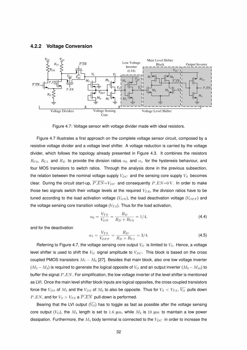
4.2.2 Voltage Conversion
Figure 4.7: Voltage sensor with voltage divider made with ideal resistors.
Figure 4.7 illustrates a first approach on the complete voltage sensor circuit, composed by a
resistive voltage divider and a voltage level shifter. A voltage reduction is carried by the voltage
divider, which follows the topology already presented in Figure 4.3. It combines the resistors
RU0, RU1 and RD to provide the division ratios α0 and α1 for the hysteresis behaviour, and
four MOS transistors to switch ratios. Through the analysis done in the previous subsection,
the relation between the nominal voltage supply VDC and the sensing core supply VS becomes
clear. During the circuit start-up, P EN=VDC and consequently P EN=0 V. In order to make
those two signals switch their voltage levels at the required VTR, the division ratios have to be
tuned according to the load activation voltage (VON ), the load deactivation voltage (VOFF ) and
the voltage sensing core transition voltage (VTS). Thus for the load activation,
α0 =VTSVON
=RD
RD +RU0= 1/4, (4.4)
and for the deactivation
α1 =VTSVOFF
=RD
RD +RU1= 3/4. (4.5)
Referring to Figure 4.7, the voltage sensing core output VO is limited to VS . Hence, a voltage
level shifter is used to shift the VO signal amplitude to VDC . This block is based on the cross
coupled PMOS transistors M7 −M8 [27]. Besides that main block, also one low voltage inverter
(M3 −M4) is required to generate the logical opposite of VO and an output inverter (M9 −M10) to
buffer the signal P EN . For simplification, the low voltage inverter of the level shifter is mentioned
as LVI. Once the main level shifter block inputs are logical opposites, the cross coupled transistors
force the VDS of M5 and the VDS of M6 to also be opposite. Thus for VS < VTS , VO pulls down
P EN , and for VS > VTS a P EN pull-down is performed.
Bearing that the LVI output (VO) has to toggle as fast as possible after the voltage sensing
core output (VO), the M4 length is set to 1.6 µm, while M3 is 10 µm to maintain a low power
dissipation. Furthermore, the M4 body terminal is connected to the VDC in order to increase the
32

PMOS transistor Vth through the body effect [24]. The input required for an inverter output to
switch voltage levels when one of the transistors is in weak inversion can be found through an
analysis similar to Equation 3.13. Attending that the current on both the NMOS and PMOS is
equal and defined by the weak inversion expression, Equation (3.5), then the output toggles for a
supply VS and an input voltage given by
VI =1
nn + np
[nnVS + npVthn − nnVthp − nnnpUT ln
(WnLpµnCoxnWpLnµpCoxp
)]. (4.6)
The subscripts n and p refer to the NMOS and PMOS parameters, respectively. Examining Equa-
tion 4.6 for a fixed inverter supply voltage VS , when Vthp is increased and Lp is decreased, the
input voltage VI required for the inverter output to toggle reduces. The sensing core inverter
presents a lower Vthp and a higher Lp than LVI. Consequently, for the same VS , the input voltage
(VO) required to toggle VO is lower than the input (VREF ) required to toggle VO.
When the VON and VOFF transitions occur, low impedance paths are established on the
inverters and main level shifter blocks as a consequence of the transistors operation in the satu-
ration region. Once the main level shifter block and output inverter are directly supplied by VDC ,
a current spike significantly higher than the steady state current can be verified on those circuits,
thus the aspect ratios applied are preferably minimized. The output inverter transistors M9 and
M10 are designed with minimum width and lengths equal to 8 µm. Once the main level shifter block
PMOS transistors operate in strong inversion at the VON transition and the NMOS operate near
the subthreshold region, the current drive capability of the PMOS is higher than the NMOS [27].
Due to this, the NMOS current drive capability has to be increased to impose an efficient pull-
down. Therefore the cross coupled PMOS transistors lengths are equal to 11 µm to reduce their
current drive capability and power dissipation on slow VO or VO transitions. Regarding the NMOS
transistors M5 and M6, their lengths are set to 5 µm to also minimize the power dissipation, but
simultaneously increase their current drive capability comparatively to the PMOS.
In order to verify the voltage sensor behaviour, the circuit is simulated under the passive sys-
tem testbench previously discussed and illustrated in Figure 4.2, with IS = 1 µA and RL =
0.3 MΩ. The chosen load resistance satisfies the intermittent system condition defined by Equa-
tion (4.2) and the low PCU current imposes an RPCU high enough for the start-up to be ensured,
Equation (4.1). The voltage divisions are made by the resistances RU0 = 95 MΩ, RU1 = 10 MΩ
and RD = 34 MΩ, selected according to Equations (4.4) and (4.5). The voltage sensor current
IV S , harvester output VDC and VS simulation plots are presented in Figure 4.8, where the load
is activated at VDC= 1.28 V and deactivated at VDC= 0.38 V. It can be confirmed that the transi-
tion moments occur when VS reaches a voltage value close to 0.3 V, as expected by the voltage
sensing core transition (VTS). The time required for the load activation is t0 = 81 ms, whilst the
active period is ∆tON= 37 ms. The average dissipated power in the voltage sensor is 8.87 nW, of
which 7.475 nW are wasted in the resistive divider. It is perceived by the analysis of Figure 4.8
that the voltage sensor current is proportional to VDC , confirming the voltage divider significant
33
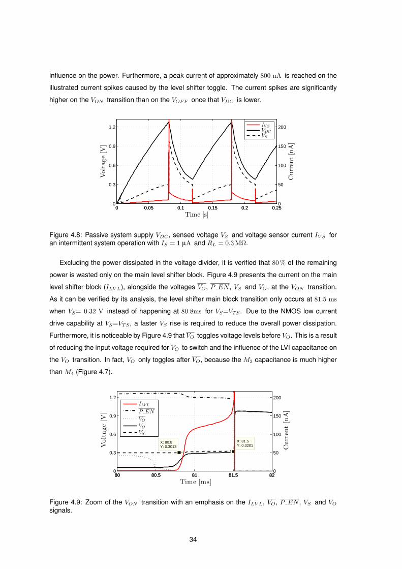
influence on the power. Furthermore, a peak current of approximately 800 nA is reached on the
illustrated current spikes caused by the level shifter toggle. The current spikes are significantly
higher on the VON transition than on the VOFF once that VDC is lower.
0 0.05 0.1 0.15 0.2 0.250
0.3
0.6
0.9
1.2
Voltage[V
]
Time [s]0 0.05 0.1 0.15 0.2 0.25
0
50
100
150
200
Current[nA]
IV S
VDC
VS
Figure 4.8: Passive system supply VDC , sensed voltage VS and voltage sensor current IV S foran intermittent system operation with IS = 1 µA and RL = 0.3 MΩ.
Excluding the power dissipated in the voltage divider, it is verified that 80 % of the remaining
power is wasted only on the main level shifter block. Figure 4.9 presents the current on the main
level shifter block (ILV L), alongside the voltages VO, P EN , VS and VO, at the VON transition.
As it can be verified by its analysis, the level shifter main block transition only occurs at 81.5 ms
when VS= 0.32 V instead of happening at 80.8ms for VS=VTS . Due to the NMOS low current
drive capability at VS=VTS , a faster VS rise is required to reduce the overall power dissipation.
Furthermore, it is noticeable by Figure 4.9 that VO toggles voltage levels before VO. This is a result
of reducing the input voltage required for VO to switch and the influence of the LVI capacitance on
the VO transition. In fact, VO only toggles after VO, because the M3 capacitance is much higher
than M4 (Figure 4.7).
80 80.5 81 81.5 820
0.3
0.6
0.9
1.2
X: 81.5Y: 0.3201V
oltage[V
]
Time [ms]
X: 80.8Y: 0.3013
80 80.5 81 81.5 820
50
100
150
200
Curren
t[nA]
ILVL
P EN
VO
VO
VS
Figure 4.9: Zoom of the VON transition with an emphasis on the ILV L, VO, P EN , VS and VOsignals.
34

118 118.1 118.2 118.3 118.4 118.5 118.60
0.1
0.2
0.3
0.4
Voltage[V
]
Time [ms]118 118.1 118.2 118.3 118.4 118.5 118.6
0
7
14
21
28
Curren
t[nA]
ILVL
VO
P EN
VS
VO
Figure 4.10: Zoom of the VOFF transition with an emphasis on the ILV L, VO, P EN , VS and VOsignals.
Comparatively to the VDC=VON , the transition at VOFF , plotted in Figure 4.10, occurs exactly
at the moment that VO toggles to 0 V, presenting a faster transition and a lower ILV L current
spike. Similarly to the previous case, the sensing core output also has a slow transition, but its
toggle to 0 V pushes VO to VS . A VO voltage spike is evidenced due to the division constants
switching from α1 to α0 during the transition. Furthermore, after the VOFF transition VS is lower
than the supply required for the reference to produce a stable voltage (≈ 0.2 V), thus VO settles
momentarily in a value lower than VS .
In order to achieve a faster VS rise after the VTS transition, the current on the low voltage
circuit (ILV ), composed by the sensing core and LVI, is discussed. As previously verified (Figure
4.6) the current on the voltage sensing core stabilizes at approximately 0.9 nA when VS=VTS .
Furthermore, as a result of its PMOS entering the cut-off region, the current on LVI decreases
from 0.25 nA to 0.5 pA, at the VO transition. Thus, it can be verified that ILV becomes lower and
stable after VS=VTS . Based on this conclusion, the loading effect of the low voltage circuit can
be used to provide a faster VS rise. In order to do it, the resistor RD is eliminated. The voltage
sensor modification is presented in Figure 4.11, which only details the voltage divider and low
voltage circuit parts. Attending at the circuit of Figure 4.11, the division ratios are now dependent
on the upper resistors RU0 and RU1, and the low voltage circuit loading effect, which is defined
as RLV = VS/ILV . Once RLV depends on VS , the resistance value used to configure the division
ratios must be given by the VS and ILV values at the VTS transition. Such resistance is defined
as RTS and is approximately 300 MΩ.
In order to verify the modified voltage sensor performance, the upper resistors of the voltage
divider are re-defined according to the previously established division ratios α0= 1/3 and α1 =
3/4. Thus, by setting RU0= 1 GΩ and RU1= 100 MΩ, the simulation result of the circuit for an
intermittent operation is presented in Figure 4.12. As it can be verified, the obtained VS rise
35

Figure 4.11: Focus on the voltage divider and low voltage circuit when RD is eliminated.
is faster than previously, refer to Figure 4.9. The transition voltages are VON = 1.286 V and
VOFF= 0.386 V, and the average power dissipated only in the voltage sensing core and level
shifter is 0.504 nW. Furthermore, the time period between the VO and P EN transitions is 0.3
ms. Once the power previously obtained was 1.4 nW and the time period was 7 ms, the modified
circuit presents a faster VS rise after the transition at VTS . The power dissipated in the voltage
divider is 0.296 nW and the highest current spike is 660 nA. Therefore, it can be concluded that
by eliminating RD of the voltage divider, the pull-down performed by the level shifter on the VON
transition is faster.
81 81.2 81.4 81.6 81.8 820
0.3
0.6
0.9
1.2
Voltage[V
]
Time [ms]81 81.2 81.4 81.6 81.8 82
0
50
100
150
200
Current[nA]
ILVL
VO
P EN
VS
VO
Figure 4.12: Zoom of the VON transition with an emphasis on the ILV , VO, VS and VO signalswhen the voltage divider has hysteresis and resistor RD= 1 TΩ.
36

4.2.3 Temperature Compensation
The proposed voltage sensor only satisfies the imposed transition specifications for a small
temperature range around the nominal design temperature of 27 oC. In order for the circuit to
satisfy the temperature range specification (−40 oC to 100 oC), it is required that the variations in
the transition voltages can be compensated without compromising the power dissipation target.
Recall that the power dissipation increases with temperature due to the threshold voltage tem-
perature dependence. For proposing a temperature compensation method, the influence of this
external parameter on the voltage sensor circuit has to be analysed.
When using ideal resistors in the voltage divider, their resistance does not change with tem-
perature, nonetheless the division ratios are affected by the current increase with temperature on
the low voltage circuit. Although the level shifter main block and the output inverter are influenced
by temperature, their effect on the transition voltage is negligible. On the main level shifter block,
this is verified by the PMOS and NMOS parameters compensation, which maintains the VO and
VO values required to toggle P EN approximately unchanged. Due to the fast P EN voltage
transition, the output inverter does not influence the sensor transitions precision. Hence the most
temperature sensitive circuit parts are the voltage sensing core and the level shifter inverter LVI.
When the voltage sensor core is used with an ideal reference voltage of 0.1 V, the transition
voltage VTS mean value is 0.306 V and varies in a ±7.2 mV interval for the temperature range,
plotted in Figure 4.13 as VTS ideal. Although the reference mean is 0.0992 V, it presents a
variation of ±8.9 mV, or equivalently a TC of 1300 ppm1, that will increase the VTS variation to
±29.5 mV, identified in Figure 4.13 as VTS real.
−40 −20 0 20 40 60 80 1000.27
0.284
0.298
0.312
0.326
0.34
VTS[V
]
Temperature [C]−40 −20 0 20 40 60 80 100
0.09
0.094
0.098
0.102
0.106
0.11
VREF[V
]
VREF
VTS idealVTS real
Figure 4.13: Temperature influence on VREF , VTS for a temperature stable VREF= 0.1 V andVTS real.
By applying the level shifter on the voltage sensing core output, yields the VTS plot of the
Figure 4.14. Comparing the VTS before and after the level shifter application, it can be seen that
a compensation is established until 40 oC. Due to the LVI capacitive effect on the sensing core,
1TC[ppm] = ((max(VREF )−min(VREF ))/VREF (T = 27oC)/(100oC+ 33oC))× 106
37

the VO transition occurs before the VO (Figure 4.9). By the analysis of Figure 4.14 it can be
concluded that the VS required to toggle VO is higher than the VS that makes VO to toggle on
temperatures below 40 oC. Thereby, the final VTS mean value increases.
−40 −20 0 20 40 60 80 1000.27
0.284
0.298
0.312
0.326
0.34Voltage[V
]
Temperature [C]−40 −20 0 20 40 60 80 100
70
392
714
1036
1358
1680
Resistance
[MΩ]
RTS
VTS initialVTS
Figure 4.14: Temperature influence on RTS and VTS before and after the level shifter application.
Based on the results of Figure 4.14, it can be stated that the ratios VON/VTS and VOFF /VTS
will not remain constant along the temperature range. In order to compensate the temperature
influence on the transition voltages (VTR), the previously defined division ratios α0 and α1 have to
be tuned according to the VTS variation. Thus the temperature influence on the RLV resistance
at the VTS transition (RTS) has to be initially analysed. Once RU0 and RU1 are ideal resistors, the
division ratios will be significantly influenced by temperature, attending at the RTS value variation
shown in Figure 4.14. In terms of the generic transition in VDC
VTR =
(RURTS
+ 1
)VTS , (4.7)
a significant VTR rise with temperature will occur, considering the VTS positive temperature de-
pendence and the denominator, RTS , negative temperature dependence. Therefore, a negative
temperature dependence, ideally higher than the RTS , has to be introduced in RU so that both
VTS and RTS influences can be overcome.
Figures 4.15(a) and 4.15(b) illustrate two voltage division circuits used in [13] and [28], re-
spectively. The first applies a PMOS to modify the divider up resistance based on the transistor
temperature dependences reported in the MOS review (section 3.1). The MOS temperature de-
pendence is configured by the transistor aspect ratio and the reference voltage VREF applied.
Once the resistors provided by the technology do not reach the mega-ohm range, the divider of
Figure 4.15(a) has to use several resistors in series or external resistors. Thus, the divider based
on a MOS string (Figure 4.15(b)) is proposed. For the example provided, it uses a series of NU
and ND diode connected PMOS to create the resistances RU and RD, respectively. When all the
transistors in the divider of Figure 4.15(b) have equal characteristics, the division ratio is simply
set by NU and ND. Implementing the transistors in RU with a different characteristics from the
38

(a) (b)
Figure 4.15: (a)Voltage divider with PMOS. (b)Voltage divider based on PMOS string.
transistors in RD creates a temperature dependence in VS . This dependence can be selected
according to the transistors threshold voltage, mobility and aspect ratio. Thus, there is no need to
use MF and a voltage reference to compensate the temperature effect.
In order to use the voltage divider of Figure 4.15(b) on the proposed sensor, the transistors
that provide RD have to be eliminated. Consequently, RU0 and RU1 are made by MOS strings.
According to [29], the gate to source voltage of a diode connected MOS varies in temperature
according to its drain current. For this implementation, the current will be imposed by the sensing
core, and its effect on the MOS string is influenced by three parameters: the transistors type, the
number of transistors (NU ) and also their aspect ratio (W/L). For the design simplification, all
the transistors in each string have equal characteristics. PMOS devices are applied, once their
mobility (µ) is lower than the NMOS and also can be made inside an individual N-well. Such
characteristics allow the number of transistors and their L to be reduced, and also do not require
the use of triple-well to keep the MOS with equal Vth. Considering the nominal temperature case,
RU0= 1 GΩ and RU1= 100 MΩ, a subthreshold biasing is required at the transition time so that
the MOS strings can generate such high resistance values. For the VON transition, the voltage
drop on RU0 is 0.9 V (VON − VTS). For the VOFF transition, the voltage drop on RU1 is only
0.1 V (VOFF − VTS). Once the PMOS overdrive voltage has to be lower than zero to impose a
subthreshold biasing, the minimum number of transistors, defined by NU , is 5 for RU0 and 1 for
RU12. The aspect ratio is chosen according to the combination of NU , W and L parameters that
make the new division ratio to stabilize VTR inside the ±10 % tolerance interval. That division ratio
can be deduced by imposing that the current on the sensing core circuit, provided by VTS/RTS ,
is equal to the current on the active MOS string. Thus, the following expression results
VTSRTS
= µCoxW
LU2T exp
((VTR − VTS)/NU − Vth
nUT
), (4.8)
2The PMOS threshold is Vth ≈ 0.24 V
39

which can be used to determine the generic division ratio α = VTS/VTR. The division ratio is
given by,
α =RTS
RU +RTS= 1− NU
VTR
(nUT ln
(L
W
VTSRTSµCoxU2
T
)+ Vth
). (4.9)
Through the analysis of Equation (4.9), it can be verified that NU presents a more preponderant
effect than W/L in the temperature dependence. To design the MOS string based resistors, firstly
a set of NU and W/L parameters is chosen, so that the voltage sensor transitions are tuned at the
nominal temperature. Then, the circuit is tested and tuned for the temperature range. By following
this procedure, the RU0 is composed by 6 PMOS with minimum width and a length of 0.6 µm.
Regarding RU1, simply one PMOS is used with a width of 0.6 µm and minimum length. Figure
4.16 illustrates the schematic and aspect ratios used in the final voltage sensor with the proposed
MOS strings. To reduce the current spike at the VON transition, a slower transition between α0
and α1 is imposed by setting the PMOS switches MSU0 and MSU1 lengths to 4 µm, while using a
minimum width.
(a)
Transistor MR0 MR1MSU0,MSU1
MCMD,M1
M2 M3 M4M5,M6
M7,M8
M9,M10
W/L[µm/µm]
0.16
0.6
0.6
0.12
0.16
4
0.16
7
0.16
10
0.16
7.5
0.16
10.2
0.16
1.7
0.16
5
0.16
11
0.16
8
(b)
Figure 4.16: (a)Final voltage sensor circuit schematic.(b)Aspect ratios applied on the final voltagesensor transistors.
To verify the complete voltage sensor temperature performance, its precision on the VON and
VOFF transitions is evaluated, Figures 4.17(a) and 4.17(b), alongside the average power Pav
and the current spike Ip reached, presented in Figure 4.17(c). Attending at Figure 4.17(a) and
4.17(b), it can be perceived that the voltage sensor transitions occur inside the defined 10 %
tolerance. In fact, the VON variation is ±33 mV and VOFF is ±11.45 mV, which corresponds to
±2.75% and ±2.86% respectively. The average power at 27 oC is approximately 0.65 nW and for
40

−40 −20 0 20 40 60 80 1001.08
1,14
1.2
1,26
1.32
Temperature [C]
VON
[V]
(a)
−40 −20 0 20 40 60 80 1000.36
0.37
0.38
0.39
0.4
0.41
0.42
0.43
0.44
Temperature [C]
VOFF[V
]
(b)
−40 −20 0 20 40 60 80 1000
2.5
5
7.5
10
Power
[nW
]
Temperature [C]−40 −20 0 20 40 60 80 100
0
0.25
0.5
0.75
1
Curren
t[µA]
Ip
Pav
(c)
Figure 4.17: (a)VON , (b)VOFF , (c)Pav and Ip for the −40 to 100 oC temperature range.
the complete temperature range, plotted in Figure 4.17(c), it is always below the 10 nW boundary.
For temperatures lower than −20 oC, the threshold voltage increase makes the voltage sensing
core transition slower, causing the level shifter main block transition to be also slower, hence the
Pav increases. The maximum current spike Ip value, depicted in Figure 4.17(c), is below 1 µA
although it rises significantly with the temperature increase, as a result of the threshold voltage
diminution and thermal voltage increase.
4.2.4 Complete Block
After proposing the voltage sensor circuit, it is required to examine its minimum response
time, steady state current, and how it performs on the Monte Carlo test and worst case process
situations. This section aim is to evaluate those specifications to infer the proposed sensor validity.
The voltage sensor minimum response time is a critical parameter, once that it will dictate the
passive system circuit performance based on the required passive system start-up time, defined
by t0, and load active time, known as ∆tON . Hence the capacitor COut and the harvester current
output IS values are changed to test the circuit for different charge and discharge times. According
41

to the results provided in Table 4.2, with the t0 and ∆tON decrease, VON and Pav increase, whilst
VOFF decreases. This behaviour is mainly explained by the referred voltage sensing core slow
response. For ∆tON= 0.312 ms, the VOFF value is close to the minimum acceptable value and for
t0= 0.152 ms, VON is out of the acceptable range. Therefore, those are the minimum charge and
active times where the circuit can maintain its precision for a nominal temperature. Furthermore,
the minimum current required to impose the passive system start-up is 1.8 nA and the maximum
steady state current is 1.092 nA, measured at VDC = 1.2 V.
Table 4.2: Minimum charge and active time analysis for nominal temperature.Test Conditions Charge Time
t0 [ms]Active Time∆tON [ms] VON [V] VOFF [V] Pav [nW]
COut [nF] IS [µA]50 1 57.42 33.19 1.149 0.392 0.6561 1 1.19 0.708 1.186 0.38 4.104
0.4 1 0.494 0.312 1.226 0.367 7.170.4 3.5 0.152 ∞ 1.328 - 1.450.1 1 0.135 0.167 1.328 0.303 11.327
To test the voltage sensor behaviour when exposed to random process variations and tran-
sistor mismatches a Monte Carlo simulation analysis is done. When simulating the circuit with
IS = 1 µA and RL = 0.3 MΩ at the nominal temperature, 94 % of the total 500 runs satisfy the
requirements. As verified by the simulation results presented in Figure 4.18, both Ip and Pav are
below their limit values, 1 µA and 10 nW respectively. However VON and VOFF are not inside
their limits for all the runs, as confirmed by Figure 4.19.
(a) (b)
Figure 4.18: Monte Carlo simulation results for (a)Pav and (b) Ip.
In order to characterize the yield for the required temperature range, Monte Carlo simulations
with 500 runs are performed for −40 oC, −25 oC, 27 oC, 90 oC and 100 oC. As previously, the
circuit is simulated for IS = 1 µA and RL = 0.3 MΩ. It is verified that for the temperature range
simulations, the yield decreases due to the Ip specification. This means that the voltage sensor
output transition is discharging the capacitor. Nonetheless, it is confirmed that passive system
42
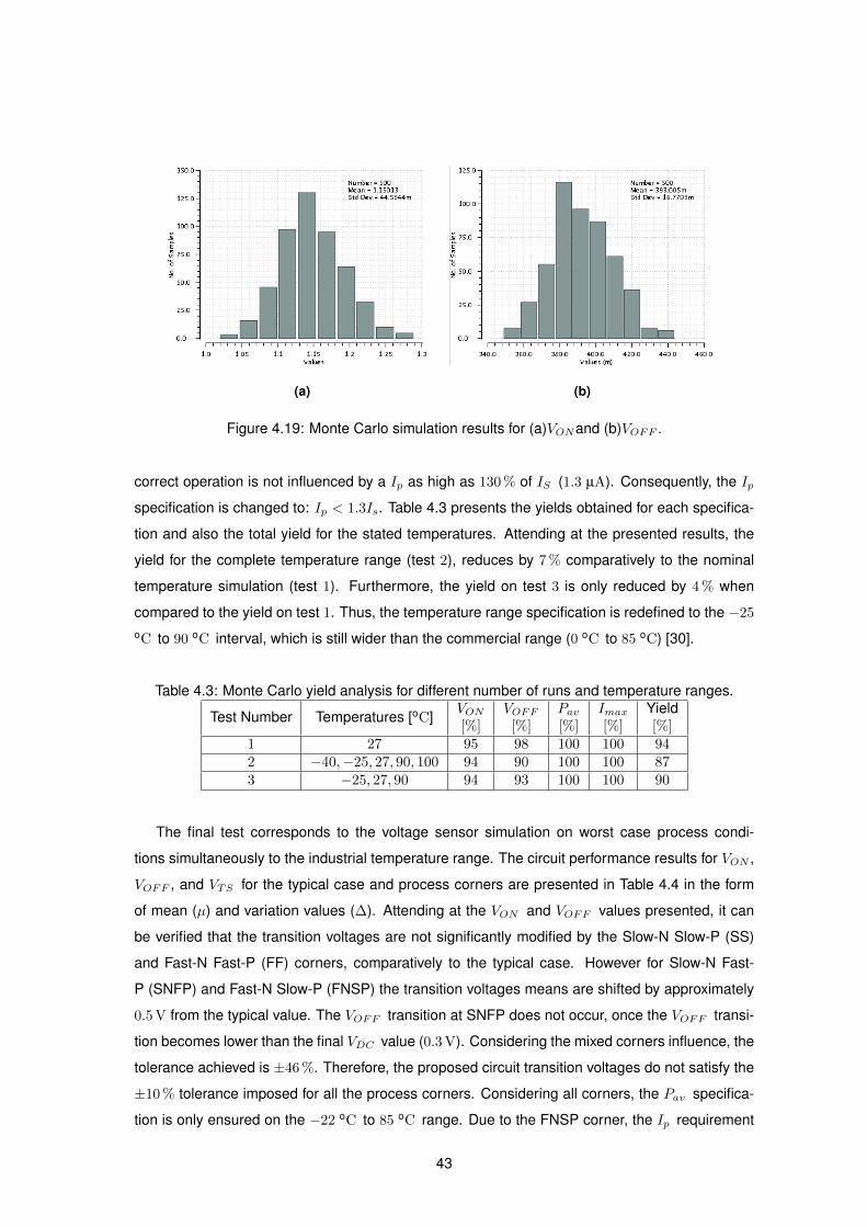
(a) (b)
Figure 4.19: Monte Carlo simulation results for (a)VONand (b)VOFF .
correct operation is not influenced by a Ip as high as 130 % of IS (1.3 µA). Consequently, the Ip
specification is changed to: Ip < 1.3Is. Table 4.3 presents the yields obtained for each specifica-
tion and also the total yield for the stated temperatures. Attending at the presented results, the
yield for the complete temperature range (test 2), reduces by 7 % comparatively to the nominal
temperature simulation (test 1). Furthermore, the yield on test 3 is only reduced by 4 % when
compared to the yield on test 1. Thus, the temperature range specification is redefined to the −25
oC to 90 oC interval, which is still wider than the commercial range (0 oC to 85 oC) [30].
Table 4.3: Monte Carlo yield analysis for different number of runs and temperature ranges.
Test Number Temperatures [oC] VON[%]
VOFF[%]
Pav[%]
Imax[%]
Yield[%]
1 27 95 98 100 100 942 −40,−25, 27, 90, 100 94 90 100 100 873 −25, 27, 90 94 93 100 100 90
The final test corresponds to the voltage sensor simulation on worst case process condi-
tions simultaneously to the industrial temperature range. The circuit performance results for VON ,
VOFF , and VTS for the typical case and process corners are presented in Table 4.4 in the form
of mean (µ) and variation values (∆). Attending at the VON and VOFF values presented, it can
be verified that the transition voltages are not significantly modified by the Slow-N Slow-P (SS)
and Fast-N Fast-P (FF) corners, comparatively to the typical case. However for Slow-N Fast-
P (SNFP) and Fast-N Slow-P (FNSP) the transition voltages means are shifted by approximately
0.5 V from the typical value. The VOFF transition at SNFP does not occur, once the VOFF transi-
tion becomes lower than the final VDC value (0.3 V). Considering the mixed corners influence, the
tolerance achieved is ±46 %. Therefore, the proposed circuit transition voltages do not satisfy the
±10 % tolerance imposed for all the process corners. Considering all corners, the Pav specifica-
tion is only ensured on the −22 oC to 85 oC range. Due to the FNSP corner, the Ip requirement
43

fails for all temperatures.
Table 4.4: Process corner and industrial temperature range influence on the VON , VOFF and VTStransition voltages mean µ and variation ±∆.
Process Corner VON (µ±∆) [V] VOFF (µ±∆) [V] VTS (µ±∆) [V]Typical 1.167± 0.033 0.397± 0.012 0.313± 0.007
SS 1.187± 0.1 0.406± 0.013 0.297± 0.02SNFP 0.654± 0.06 - 0.197± 0.023
FF 1.173± 0.081 0.396± 0.032 0.329± 0.0485FNSP 1.755± 0.072 0.614± 0.029 0.44± 0.05
Table 4.5: Process corner and industrial temperature range influence on the maximum VREF andVTS for a temperature stable VREF= 0.1 V. Results detailed in the form of mean µ and variation±∆.
ProcessCorner
VREF(µ±∆) [mV]
Ideal VTS(µ±∆) [mV]
Typical 97.8± 8.45 306± 7SS 96.6± 4.6 302± 4
SNFP 65.3± 6 267± 4FF 102.4± 12.6 310± 11
FNSP 136± 9.5 350± 11
In fact the verified shifts are caused by the mixed corners effect on the sensing core transition
(VTS), refer to Table 4.4. Once the division ratios define a linear relation between VTR and VTS ,
the shifts in VTS are propagated to the transition voltages VON and VOFF . In order to justify
the VTS variation, both the reference circuit and the voltage sensing circuit with an ideal 0.1 V
reference, are simulated under process corners and temperature, yielding the results of Table
4.5. It is verified that the process corners influence on VREF and on the ideal VTS , is similar to
the reported for VON , VOFF and VTS . The process corners affect VREF and the ideal VTS in the
same way, once that both depend on Vthp − Vthn and µn/µp. Such dependence is confirmed by
the expressions that defines VREF , Equation (3.13), and VTS , given by
VTS =nn + npnn
VREF +nnVthp − npVthn
nn+ npUT ln
(µnCoxnµpCoxp
WnLpWpLn
). (4.10)
The presented expression is obtained similarly to Equation (4.6). Compared to the typical process,
the mentioned Vth difference and µ ratio, increases on FNSP and decreases on SNFP. Thereby
explaining the same influence on the voltages identified in Tables 4.4 and 4.5.
As a concluding remark, it can be stated that the temperature compensation is effective for
typical conditions and for process variations imposed by Monte Carlo analysis. However, on the
extreme case of the process corners, mainly on SNFP and FNSP, the transition voltages present
a shift higher than the tolerance defined in the research goals.
44

4.3 Voltage Limiter
In this section, the second part of the developed PCU is reviewed following a similar analysis
to the previous section. The block proposed to perform the voltage limiting is based on the high
level circuit presented in Figure 4.20. This uses the same voltage sensing method as the voltage
sensor, but without hysteresis. To create the discharge current Idisc mentioned in the voltage
limiters review (section 2.3.2), a low impedance path is established by Mdisc. To successfully
control Idisc, an inverter (M3 −M4) is used as an amplifier of the limiter sensing core output VO.
Power down switches controlled by the sensor output P EN are included in the design to block
the limiter operation and the current flow while the load is not active. The schematic of Figure
4.20 depicts the voltage limiter when the load is active. At that phase, the limiter is sensing VDC .
When the system enters the voltage limiting mode, the limiter is required to stabilize VDC in the
VLim range (1.35 V to 1.65 V), defined in subsection 4.1.2.
Figure 4.20: Voltage limiter structure when active. P EN powers down the limiter when high.
4.3.1 Circuit Discharge and Temperature Compensation
The complete voltage limiter schematic is shown in Figure 4.21(a), where the up resistor RUL
is implemented by a MOS string to compensate the temperature effect. The transistors in RUL
are identified as MUL once they present equal characteristics. The voltage sensing core uses
the same circuit as the voltage sensor. The discharge control part uses the M3 −M4 inverter
as an amplifier to control the discharge current Idisc through Vdisc. Transistors MS1 −MS2 are
the power down switches. The P EN transition from VDC to zero activates the limiter voltage
sensing function. When VDC=VLim, VO toggles from zero to VS , which decreases Vdisc. The
consequent Idisc rise forces VDC to reduce. Thus a feedback loop based on the voltage supply
is verified.
The voltage limiter design method is based on the compromise established between the power
dissipation while idle, the circuit response time and the maximum discharge current. The first is
45

(a)
Transistor MUL MC MD M1 M2 M3 M4 Mdisc MSO MS1 MS2
W/L[µm/µm]
0.4
2
0.16
7
0.16
10
0.16
10
0.16
10
0.16
2
0.16
8
0.16
0.12
2
0.12
0.16
0.12
0.16
0.12
(b)
Figure 4.21: (a) Proposed voltage limiter circuit schematic. (b) Aspect ratios of the transistors inthe schematic.
required to ensure the passive system power efficiency, once that the limiter is simply sensing the
voltage at that phase, but the load is active. The other factors are necessary to ensure that in a
voltage limiting operation the circuit VLim does not surpass the defined range. According to that,
the applied aspect ratios for the voltage limiter are presented in Table 4.21(b), where the voltage
sensing core used is designed similarly to the explained in the voltage sensor section. The aspect
ratio of the transistors used in the discharge control inverter is higher than for the sensing core
inverter to increase the gain. Mdisc width is lower than MSO to minimize the leakage and increase
Idisc when the low impedance path is activated. With the applied aspect ratios, the maximum
achievable Idisc is approximately 80 µA. Bearing the analysis made for the voltage sensor, the
limiter division ratio αL has to satisfy
αL =RTS
RTS +RUL=
VTSVLim
= 1/5 (4.11)
where RTS is the sensing core resistance at the VS = VTS transition. Recalling that RTS ≈
300 MΩ at the nominal temperature, the up resistance is RUL = 1.2 GΩ, based on Equation
(4.11). Figure 4.22(a) shows the VDC , VS Vdisc and Idisc plots for an ideal RUL= 1.1 GΩ, RL=
0.3 MΩ and IS= 10 µA. IS and RL are chosen according to the limiting condition defined by
Equation (4.3). Attending at those results, VLim is close to 1.5 V and VDC stabilizes in the
acceptable range by making Idisc= 4 µA. However, it can be verified by Vdisc, that the limiter
response is started at VDC= 1.4 V and the system presents a transient response caused by the
46

feedback loop. This factor is mainly limited by the sensing core long response time, which causes
a VDC propagation delay through VO. Furthermore, VLim is different from VDC= 1.4 V, because
the sensing core output at VS=VTS is not sufficiently high to reduce VDC . Thus, Idisc must be
activated for the lowest VDC value that makes VLim to be contained inside the acceptable range.
0 0.005 0.01 0.0150.15
0.3
0.45
0.6
0.75
0.9
1.05
1.2
1.35
1.5
1.651.65
Voltage[V
]
Time [s]0 0.005 0.01 0.015
0
1
2
3
4
5
6
7
8
9
10
11
Curren
t[µA]
Idisc
VDC
Vdisc
VS
(a)
0 0.005 0.01 0.015 0.02 0.0250.3
0.45
0.6
0.75
0.9
1.05
1.2
1.35
1.5
1.651.65
Time [s]Voltage[V
]
VDC
Vdisc
VS
(b)
Figure 4.22: Voltage limiter transient response for RL = 0.3 MΩ, (a) IS = 10 µA and (b) IS =20 µA.
When the source current is increased to 20 µA, but RL remains the same, a longer transient
response is verified, as presented in Figure 4.22(b). To obtain the presented plots, RUL is raised
to 1.2 GΩ to attenuate the oscillatory regime. This extreme case is due to the amplifier short linear
range and the VDC to VO propagation delay. According to Figure 4.22(b), VDC only stabilizes in
1.6 V at 0.023 ms.
Following the design method proposed for the voltage sensor, a MOS string is applied to
compensate the temperature effect on VLim. By doing that, RUL resistance is provided by 8
PMOS with a width of 0.4 µm and a length of 2 µm. To verify the temperature effect on VLim the
circuit is simulated with IS = 10 µA and RL = 0.3 MΩ, yielding the results of the Figure 4.23(a).
Attending at those plots, it is confirmed that both the maximum VDC (VLim) and final VDC satisfy
the ±10 % tolerance imposed. In fact, the VLim tolerance to the temperature is ±6.9 mV, which
corresponds to ±4.5 %. Furthermore, the RUL based on a MOS string provides a faster transient
response comparatively to an ideal resistor, as confirmed by the simulation results illustrated in
Figure 4.23(b). Setting IS = 20 µA as for Figure 4.22(b), the final voltage limiter is able to stabilize
VDC in less than 1/6 of the time required when ideal resistors are applied. That is verified once
RUL is able to adapt itself when VDC decreases. Such fact is confirmed by the RUL increase at
approximately 2.6 ms in Figure 4.23(b).
47

−40 −20 0 20 40 60 80 1001.48
1.5
1.52
1.54
1.56
1.58
1.6
1.62
1.64
Temperature [C]
Voltage[V
]
VDC finalVLim
(a)
0 1 2 3 4 5
x 10−3
0
0.15
0.3
0.45
0.6
0.75
0.9
1.05
1.2
1.35
1.5
1.65
Voltage[V
]
Time [s]0 1 2 3 4 5
x 10−3
1.1
1.15
1.2
1.25
1.3
1.35
1.4
1.45
1.5
1.55
1.6
1.65
Resistance
[GΩ]
RUL
VDC
Vdisc
VO
(b)
Figure 4.23: (a) VLim transition and final VDC voltages for the temperature range after the tem-perature compensation is applied. (b) Voltage limiter transient response for IS = 20 µA andRL = 0.3 MΩ after applying the MOS string.
4.3.2 Complete Block
To finalize the voltage limiter analysis, its performance for process corners, alongside the
minimum VDC rise time ∆tL and maximum IS , are evaluated. Recalling the definition on section
2.2, ∆tL defines the time period between the load activation and VDC=VLim. The circuit is not
submitted to a Monte Carlo simulations in this section, once that such analysis is done for the final
PCU in section 4.4.
Besides the precision required for the VLim transition, the maximum power that can be dissi-
pated by the circuit is one of the fundamental limiter specifications. To evaluate it, the maximum
Idisc is assessed for nominal conditions and it is verified that the discharge current cannot sur-
pass 74 µA. Furthermore, the minimum ∆tL is = 0.2 ms. In order to verify the possible limiter
influence on the voltage sensor operation, the total current required by the limiter is measured
when it is turned off, P EN= VDC , and idle, P EN= 0 V. When the voltage limiter is off, a cur-
rent of 0.304 nA is required and when it is idle, the current increases to 0.875 nA, which is not
negligible compared to a steady state current of 1.1 nA on the sensor during the load active time.
When the circuit is simulated for process corners and temperature range (−40 to 100 oC) for
an IS = 10 µA and RL = 0.3 MΩ, VLim behaves as presented in Table 4.6. As expected by
the temperature simulation, refer to Figure 4.23(a), VLim mean (µ) and variation (∆) are higher
than for the final VDC . Attending at the results of Table 4.6 it is verified that the VLim precision
specification is met for all corners except for SS, where it is 17 %. As the voltage limiter relies on a
voltage sensing core similar to the voltage sensor, the mixed corners influence on VLim is equal
to the verified for VON and VOFF (Table 4.4).
48
Table 4.6: Process corner and temperature range (−40 oC to 100 oC) influence on the final VDCand VLim voltages mean µ and variation ∆.
Process Corner VDC final(µ±∆) [V]
VLim(µ±∆) [V]
Typical 1.518± 0.035 1.535± 0.069SS 1.474± 0.165 1.533± 0.25
SNFP 0.842± 0.068 1.2± 0.0002FF 1.556± 0.094 1.558± 0.093
FNSP 2.19± 0.063 2.197± 0.057
Target [1.35; 1.65] [1.35; 1.65]
4.4 Final PCU
Through the analysis presented in the previous sections, the proposed voltage sensor and
limiter blocks are ensured to operate as desired when tested separately. In this section, the two
designed blocks are combined for the final PCU circuit and its behaviour is assessed for both pre
and post-layout cases. The final circuit results are compared to the state-of-the-art PCUs and
voltage sensors.
4.4.1 Combined Blocks Evaluation
In this subsection, the final PCU circuit, based in the structure presented in Figure 4.1, is eval-
uated to infer the possible variations in the previously assessed voltage sensor and limiter speci-
fications. The proposed circuit is simulated under the same conditions used for testing the blocks
separately, where IS = 1 µA for an intermittent operation and IS = 10 µA for voltage limiting,
yielding the results of Table 4.7. The remaining parameters RL = 0.3 MΩ and COut = 50 nF are
equal for both operations, thereby emulating the situation where the passive system is exposed to
different input powers. Comparing the presented results, the transition precision for the nominal
Table 4.7: Voltage sensor and limiter specifications obtained for the separate and combined cir-cuits tests.
OperatingMode Intermittent Voltage
Limiting
Specification VON[V]
VOFF[V]
Pav[nW]
Ip[µA]
t0[ms]
∆tON[ms]
VLim[V]
∆tL[ms]
TestType
Separate 1.149 0.392 0.656 0.681 57.42 33.2 1.485 2.99Combined 1.149 0.392 0.847 0.641 57.4 32.7 1.485 3.29
temperature is not affected once that the activation and deactivation voltages, VON and VOFF , re-
main equal and also the VDC maximum value, VLim. As the PCU total current IPCU becomes the
sum of the voltage sensor (IV S) and limiter (IV L) currents, Pav is the most influenced specifica-
tion. By combining the two circuit blocks, the system charge (t0 and ∆tL) and discharge (∆tON )
times are modified. That occurs, once the PCU resistance, defined as RPCU = VDC/IPCU , de-
creases when compared to the simulations for the separate blocks. During the system start-up,
49

the voltage limiter is off, thus IV L contribution to IPCU is lower than IV S , confirming the small
difference in the t0 charge times. Once IV L= 0.9 nA and IV S= 1.1 nA for VDC= 1.2 V, RPCU
decreases when compared to separate block test. Hence, the discharge period ∆tON and the
charge period ∆tL are modified.
0 0.05 0.1 0.15 0.20.35
0.465
0.58
0.695
0.81
0.925
1.04
1.155
1.27
1.385
1.5
Voltage[V
]
Time [s]0 0.05 0.1 0.15 0.2
0
0.57
1.14
1.71
2.28
2.85
3.42
3.99
4.56
5.13
5.7
Current[µA]
IPCU
VDC
Figure 4.24: PCU simulation for IS= 10 µA during 0.1 s and IS= 1 µA afterwards.
To further evaluate and confirm the PCU correct behaviour, Figure 4.24 displays the simulation
results of the circuit when simulated with a IS that initially provides 10 µA during 0.1 s and then
settles on 1 µA. It is expected that the circuit applies a voltage limiting during the first 0.1 s and an
intermittent operation afterwards. Analysing the referred plot, the moment when VON is reached
can be identified by the first current spike mark. In turn, that leads to the P EN transition from
VDC to zero, which causes the voltage limiter activation, confirmed by the IPCU stabilization on
5.1 µA. At 0.1 s, VDC no longer requires to be limited, thus the system leaves voltage limiting and
returns to an intermittent operation, turning off the load at VOFF and confirming the PCU ability
to operate on different modes.
Table 4.8: Yield analysis of the Monte Carlo results for the final PCU when testing the intermittentoperation.
Runs Temperatures[oC]
VON[%]
VOFF[%]
Pav[%]
Ip[%]
Yield[%]
Previous Yield[%]
500 27 97 99 100 100 96 94500 −25, 27, 90 97 95 100 100 93 90
In order to verify the PCU circuit robustness when exposed to random process variations and
mismatches, Monte Carlo tests are done. The voltage sensor performance is characterized by
simulating the circuit for IS = 1 µA andRL = 0.3 MΩ on the redefined temperature range (−25 oC
to 90 oC). 500 runs are used for each temperature. Attending at the results presented in Table
4.8(a), the final yield for the nominal temperature test is higher than the obtained for the separate
voltage sensor test by 2 %. When testing on the −25 oC to 90 oC range, the obtained yield is
50

also higher than the previous. Such differences are explained by the modification of t0 and ∆tON ,
stated in Table 4.7.
Table 4.9: Yield analysis of the Monte Carlo results for the final PCU when testing the voltagelimiting operation.
Runs Temperatures[oC]
IS[µA]
VLim[%]
Yield[%]
500 27 10 99 97500 −25, 27, 90 10 92 90100 −25, 27, 90 20 80 74
To test the voltage limiting operation mode, the PCU is simulated for the same passive system
parameters, except IS that is set according to the values indicated in Table 4.8(b) alongside the
obtained yields. Analysing the presented results, the circuit yield for the nominal temperature is
97 % and for the proposed temperature range it is 90 %. However, when IS = 20 µA the yield
becomes lower than 80 %. In fact, by only changing IS , the charge time ∆tL is reduced through
the increase of the maximum charging voltage (Appendix A). Therefore, the limiter specifications
are only ensured on the −25 oC to 90 oC range for a minimum ∆tL= 3.3 ms.
Regarding the process corners, the PCU specifications do not present significant changes
when compared to the results previously detailed in the Tables 4.4 and 4.6.
4.4.2 Layout and Results
Based on the previous subsection, it is concluded that the PCU satisfies the specifications
imposed for a typical process with a yield equal to 90 %, thus a layout implementation is done.
Along this subsection, the layout design method is described and at the end the results obtained
from the extracted model simulation are presented.
Besides the VDC , ground and P EN connections required, shown in Figure 4.1, also the
output P EN is added for testing purposes. Considering the low speed of the proposed PCU, the
only metrics imposed are the minimization of the occupied area and metal types used. Besides
that, the circuit is isolated through ground connected guard rings. The complete circuit without
pads solely uses 2 metal types, where the metal 1 is mostly applied for horizontal connections
and metal 2 for vertical. The width of the applied metal paths follows the 1 µm/mA empirical rule
stated in [31]. Once the maximum expected current is approximately 80 µA, minimum width can
be used.
Figure 4.25 illustrates the PCU layout without pads, where four distinct circuit blocks can be
identified, the voltage sensor at the top, the limiter at the bottom and the respective reference
circuits in the middle. The VDC and P EN pins are placed at the left and right of the circuit, re-
spectively, whilst the P EN and ground are at the upper and lower circuit extremes, respectively.
Specific guards rings are applied to the reference circuits so that the generated voltage is less
influenced by the sensor and limiter voltage transitions. The MOS strings used for RU0 and RUL
51

Figure 4.25: Layout implementation of the proposed PCU.
52

Figure 4.26: Layout implementation of the proposed PCU with pads.
have to satisfy the minimum distance between their N-wells, because each well is biased at dif-
ferent potentials. Hence, those PMOS transistors are applied around the respective circuit block
transistors to satisfy the distance requirement and also reduce the circuit area. Due to the dimen-
sions chosen, only the voltage limiter transistor MSO (2 µm/0.12 µm) is applied with two fingers to
reduce the occupied area. To contain the PCU, another ground connected guard ring is applied.
The total area used without pads is 32.59 µm by 37.27 µm, equivalently 1215 µm2, whereas with
the pads inclusion it becomes 32310 µm2, illustrated in Figure 4.26.
In order to ensure that the circuit properties are maintained after the layout design, the PCU is
simulated based on its extracted parameters. Applying the same external parameters values used
before to impose the intermittent and voltage limiting operating modes, the post-layout results
satisfy the imposed specifications, as confirmed by Table 4.10. In fact the post-layout results do
not present a significant change to those obtained by the pre-layout simulations, except for the
peak current Ip that increases by 0.2 µA.
Due to the addition of parasitic capacitances previously not accounted on the circuit level
simulations, the ideal minimum times that ensure the PCU transition precisions on the nominal
temperature are changed according to Table 4.11. The differences are more significant for the
53

Table 4.10: Comparison of the pre and post-layout simulation results for the intermittent andvoltage limiting modes on the nominal temperature.
Operating Mode Intermittent VoltageLimiting
Specification VON[V]
VOFF[V]
Pav[nW]
Ip[µA]
t0[ms]
∆tON[ms]
VLim[V]
∆tL[ms]
TestType
Pre-Layout 1.149 0.392 0.847 0.641 57.4 32.7 1.485 3.29Post-Layout 1.15 0.392 0.868 0.838 57.6 32.8 1.486 3.31
charge t0 and discharge times ∆tON as a result of applying the voltage level shifter to convert
the sensing core output.
Table 4.11: Voltage sensor and limiter minimum time specifications obtained for the pre and post-layout simulations on nominal temperature.
Specification Min. t0[ms]
Min. ∆tON[ms]
Min. ∆tL[ms]
TestType
Pre-Layout 0.152 0.312 0.2Post-Layout 0.162 0.327 0.2
Final Monte Carlo simulations are run on the −25 oC to 90 oC temperature range for RL = 0.3
MΩ, COut = 50 nF and IS = 1 µA or IS = 10 µA considering intermittent or voltage limiting
tests, respectively. The results produced are displayed in Table 4.8, in terms of the mean µ and
amplitude of the variation ∆ for each specification. Furthermore the 3σ value is also detailed to
compare with ∆. By evaluating ∆, the tolerance achieved for each specification can be inferred,
yielding ±12 % for VON , ±13 % for VOFF and ±17 % for the VLim. However the most probable
tolerances, given by 3σ, are ±10.5 %, ±11.3 % and ±15 %. It is also verified that the average
power dissipated is always below 6.2 nW. Thus, the final yield for an intermittent operation is
88 % and for the voltage limiting is 92 %. Comparatively to the pre-layout situation, the intermittent
operation yield is reduced by 2 %, which can be explained by the referred increase of the minimum
response time of the voltage sensor.
Table 4.12: Comparison of the yields obtained for pre and post layout on the −25 oC to 90 oCrange. The mean (µ), the total (∆) and the 3σ variations are reported for each specification.
Specification VON[V]
VOFF[V]
Pav[nW]
Ip[µA]
VLim[V]
Target [1.08; 1.32] [0.36; 0.44] < 10 < 1.3 [1.35; 1.65]µ± ∆ 1.171± 0.145 0.396± 0.052 3.1± 3.03 0.889± 0.296 1.528± 0.26
3σ 0.126 0.045 2.7 0.261 0.225Yield[%]
89 96 100 100 9288
PreviousYield [%]
93 92
The results obtained by simulating the extracted circuit for MOS process corners and temper-
ature range (−25 oC to 90 oC) are presented in Table 4.13. For a more detailed analysis, the
54

results obtained for temperature and corners are presented in the Appendix B. The transition volt-
ages variations are shown alongside the maximum values achieved for the power Pav and peak
current Ip. The obtained results do not present significant changes from the previous corner anal-
ysis. Thus a maximum ±3.3 % precision variation is verified for the transition and limiting voltages
on the typical case. Furthermore, the variations obtained for those specifications are all below the
defined ±10 % tolerance, except for the VLim, which is ±13 % for SS. Considering the inaccuracy
verified for the mixed corners, the worst case variation is ±55 %, on VON . Regarding Pav and
IP , the maximum values achieved are above the imposed limits, reaching 14.1 nW and 2.4 µA
respectively.
Table 4.13: Results obtained for post-layout simulations on MOS process corners and −25 oC to90 oC range.
Corner VON(µ±∆) [V]
VOFF(µ±∆) [V]
PavMax. [nW]
IPMax. [µA]
VLim(µ±∆) [V]
Typical 1.167± 0.032 0.396± 0.012 5.8 0.92 1.5± 0.05SS 1.188± 0.104 0.405± 0.012 10.1 0.88 1.498± 0.19
SNFP 0.655± 0.061 − 0.92 0.2 0.863± 0.109FF 1.174± 0.08 0.396± 0.032 13.76 1.2 1.546± 0.094
FNSP 1.755± 0.071 0.613± 0.028 14.1 2.4 2.18± 0.068
Target [1.08; 1.32] [0.36; 0.44] < 10 < 1.3 [1.35; 1.65]
4.4.3 Discussion
The designed PCU, Figure 4.1, combines the voltage sensor and limiter circuits illustrated in
the Figures 4.16(a) and 4.21(a). Both circuits are based on subthreshold circuits to perform the
voltage sensing. Those are referred as the voltage sensing cores and are composed by a CMOS
inverter connected to a 2T reference. To match the core transition voltage to VON , VOFF and
VLim values, voltage dividers are applied. Those are based on the voltage sensing core circuit
resistance and on a resistance that connects the nominal supply (VDC) to the sensing core supply.
This method allows the average power to be reduced, by eliminating the use of the voltage divider
down resistor and by providing a voltage boost on the sensing core output. The divider up resistor
is based on a string of diode connected MOS that compensate the remaining circuit temperature
variations. This topology achieves a lower power dissipation when compared to the differential
pair based sensing. However it requires the application of a level shifter circuit to convert the
output of the low voltage comparator.
During an intermittent operation, the final PCU achieves a maximum steady state current of
2 nA at 1.2 V in the discharge phase, where the voltage limiter and sensor use 0.9 nA and 1.1 nA,
respectively. Nonetheless, at the transition moments, specifically when VDC=VON , current spikes
as high as 1.3 times the current source value are verified. To reduce the influence of the current
rise during the transition, the transition time is minimized, yielding an average power dissipated
55

Table 4.14: Comparison of the PCU specifications.Reference This Work [9] [15]
Load Activation 1.2 V 1.75 V 2.75 VLoad Deactivation 0.4 V 1.2 V 1.9 V
PCU BlocksSensor,Limiter,
Reference
Sensor,Limiter,
Reference,Regulator
Sensor,Limiter,
Reference,Regulator
PCU Current 2 nA80 nA@ charge100 µA@ disc. 1.5µA
below 6.2 nW. Table 4.14, compares those specifications to the state-of-the-art PCUs literature.
Analysing the presented results, the designed circuit achieves a maximum current below 1/10 of
the minimum current achieved on the state-of-the-art [9]. However, the proposed PCU does not
include a regulator, which would impose a higher current on the discharge phase, as happens
on [9]. By the Monte Carlo simulations performed, the VON and VOFF precisions are not ensured
for passive systems that present charge and active times below 57 ms and 33 ms. Furthermore,
assuming a continuously rising supply voltage, the time difference between the sensor and limiter
activation instants (∆tL) is limited to 3.3 ms, which for the chosen load resistance (RL = 0.3 MΩ)
corresponds to a maximum discharge current of 5 µA. The discharge current can be increased
to a maximum of 80 µA, as long as ∆tL is at least 3.3 ms. This result is largely inferior to the
ideally required 1 mA [18]. Nonetheless to achieve such value, the PCU power dissipation when
the voltage limiter is idle would have to compromise the Pav specification target. Although the
state-of-the-art results [18] do not explicitly specify the maximum discharge current, the limiter
idle current is 150 nA, whilst for this work is 0.9 nA.
Table 4.15: Comparison of the transition voltage precision for temperature and corners.
Reference ThisWork
PreviousWork [13] [17] [16]
Current 2 nA@ 1.2 V
3.3 nA@ 1.2 V
6.8 nA@ 1.1 V
NA
Temperature Range [−25 90] oC [−25 125] oC [−40 105] oC [−40 120] oC
Tolerance Temp. ±10 % ±7.5 % ±4.8 %±22 %
PVTCorners 55 % ±42.6 %
Area 1215 µm2 w/o pads32310 µm2 NA 7200 µm2 27000 µm2 w/o pads
Technology 0.13 µm 0.13 µm 0.065 µm 0.5 µm
Due to the charge and discharge time influence on the results, the initially proposed temper-
ature range is decreased to −25 oC to 90 oC. When the proposed circuit is submitted to that
temperature range, VON , VOFF and VLim precisions satisfy a ±10 % tolerance around their nomi-
nal values, whereas the average power remains below 6.2 nW. These results are proven by a 88 %
yield on the Monte Carlo simulations. Comparatively to the voltage sensors literature, presented
56

in Table 4.15, this work specifications match those in the state-of-the-art. Nonetheless, the tran-
sition tolerance increases to ±55 %, due to the mixed corners influence on the sensing core. This
characteristic makes the proposed PCU not suitable, according to the research goals. When com-
pared to the previous work [13], the precision results obtained are worse, once that [13] uses low
leakage transistors to reduce the power dissipation and applies external resistors to compensate
the inaccuracy introduced by the mixed MOS process corners.
The specifications initially imposed are compared to the results obtained by the Monte Carlo
analysis in the Table 4.16. The Monte Carlo results are used instead of the corner results, because
those represent the most probable process variation events. Attending at Table 4.16, the average
power is below the target and the worst transition precision can reach ±17 %, which does not
meet the target. However, it is verified that 88 % of the circuits present a tolerance below, or equal
to ±10 %. The temperature range is decreased by 25 oC comparatively to the initially imposed.
Furthermore, the peak current is higher than the imposed. Nonetheless it is proven that it does
not influence the passive system correct operation, because the current spikes are sufficiently fast
to not decrease the capacitor voltage.
Table 4.16: Comparison of the specifications achieved by Monte Carlo analysis and the targetsproposed in the research goals.
Specification Target AchievedTransitionTolerance ±10% ±17%
AveragePower 10 nW 6.2 nW
PeakCurrent 1 µA 1.2 µA
Temp.Range [−40 100] oC [−25 90] oC
57

58

5Conclusions
Contents5.1 Work Conclusions . . . . . . . . . . . . . . . . . . . . . . . . . . . . . . . . . . . 605.2 Future Work . . . . . . . . . . . . . . . . . . . . . . . . . . . . . . . . . . . . . . 61
59

5.1 Work Conclusions
This work proposes the design of a PCU implementable on passive systems based on low
power external energy sources. Through the state-of-the-art analysis, it is verified that Radio
Frequency (RF) harvesters present one of the lowest power outputs. That type of harvesters is
able to provide 1 µA to a 1.2 V load with an input power of 10 µW (−20 dBm). Thus a PCU able
to supply a load circuit based on such low power is required.
In order to verify the role of a PCU in a system composed by an energy harvester and a load
circuit, known as a passive system, a study of its high level model is proposed. This allows the
characterization of three different system operations: intermittent, continuous and voltage limiting,
which is a special case of the continuous. The intermittent case proves to be more advantageous
for low power applications, once it requires the lowest input power. The voltage limiting is the
extreme operation mode, where the PCU must limit the power delivered to the load, so that it is
not damaged. Consequently the PCU circuits are chosen so that those two operating modes can
be implemented.
Based on the PCU state-of-the-art review, the most complete PCUs comprise three functional-
ities: harvested energy evaluation, load activation and power delivery. In order to completely fulfil
those, a voltage sensor, limiter and regulator are required. However, in this work only a voltage
sensor is needed, to apply the intermittent operation, and a voltage limiter for the limiting opera-
tion. The circuits are designed in the UMC 130 nm technology with high speed transistors only.
The load is activated at 1.2 V (VON ), deactivated at 0.4 V (VOFF ) and its supply cannot surpass
the 1.5 V (VLim).
The voltage sensor relies on a voltage sensing core circuit based on subthreshold biasing to
achieve a low power dissipation, required for the passive system to be power efficient. The core
combines a CMOS inverter connected to a modified 2T reference circuit, which produces a 0.1 V
stable supply. When compared to the circuit most applied in the PCU literature to implement the
voltage sensing, the differential pair, the proposed sensor achieves a further power dissipation
reduction. However a voltage level shifter has to be applied to create an output control signal
with the same amplitude as the nominal voltage supply. To provide the sensing core supply
voltage and the hysteresis sensor behaviour, two voltage dividers are used. Those are based
on the resistance implemented by a string of diode connected MOS and on the sensing core
equivalent resistance. By applying the correct number of MOS and aspect ratio, the VON and
VOFF transitions are compensated in temperature. The voltage limiter applies a similar sensing
core and voltage divider circuit to evaluate the voltage supply value. Then based on the sensing
core output, a low impedance path is activated, allowing a maximum discharge of 80 µA. Due
to the sensing core slow response, Monte Carlo analysis prove that the circuit performance is
severely dependent on the voltage supply charge and discharge rates.
60

The final circuit is implemented at layout level and the specifications summary is presented in
Table 5.1. In order to reduce the PCU charging and discharge times influence, the temperature
range is redefined to −25 oC to 90 oC, where the transition voltages present a ±10 % tolerance.
The average power dissipated during the intermittent operation at nominal temperature is 0.9 nW,
whilst the maximum power is 6.2 nW for the defined temperature range. The Monte Carlo simula-
tions prove that 88 % and 92 % of the circuits operate correctly on intermittent and voltage limiting
modes, respectively. However, when simulated on MOS process corners, the maximum tolerance
is increased to ±55 % due to a high sensitivity of the sensing core to mixed process corners, whilst
the maximum power becomes 14 nW.
Table 5.1: Final PCU specifications summary.Technology 0.13 µm
Area 32 310µm2
TemperatureRange [−25 90] oC
TransitionsTolerance ±10 %
Power 6.2 nWYield 88 %
5.2 Future Work
The proposed PCU is tested at simulation level for ideal harvester and load circuit models. A
following step for this work is to evaluate the PCU performance with harvester and load models
closer to the real circuits specifications. As an example, the load circuit shall be implemented as
a time-varying non-linear resistor. After doing such verification, the circuit can be implemented
at physical level. At this stage, the designed IC can be combined with a real harvester and load
circuit, allowing the future results to be compared with the ones presented in this document.
It is verified that the mixed process corners affect significantly the PCU performance, by shift-
ing the voltage sensing core transition voltage. Such effect is due to the dependence of the tran-
sition voltage on the thresholds of the NMOS and PMOS transistors that compose the sensing
core. If necessary to correct such effect, another comparator circuit has to be proposed, because
the CMOS inverter threshold is significantly affected by mixed process corners.
61

62

Bibliography
[1] R. Vullers, R. van Schaijk, I. Doms, C. Van Hoof, and R. Mertens, “Micropower energy
harvesting,” Solid-State Electronics, vol. 53, no. 7, pp. 684–693, 2009. [Online]. Available:
http://linkinghub.elsevier.com/retrieve/pii/S0038110109000720
[2] J. Yi, W. H. Ki, and C. Y. Tsui, “Analysis and design strategy of UHF micro-power CMOS rec-
tifiers for micro-sensor and RFID applications,” IEEE Transactions on Circuits and Systems
I: Regular Papers, vol. 54, no. 1, pp. 153–166, 2007.
[3] A. Shameli, A. Safarian, A. Rofougaran, M. Rofougaran, and F. D. Flaviis, “Power harvester
design for passive uhf rfid tag using a voltage boosting technique,” IEEE Transactions on
Microwave Theory and Techniques, vol. 55, no. 6, pp. 1089–1097, June 2007.
[4] G. Papotto, F. Carrara, G. Palmisano, and S. Member, “A 90-nm CMOS Threshold-
Compensated RF Energy Harvester,” IEEE Journal of Solid-State Circuits, vol. 46,
no. 9, pp. 1985–1997, 2011. [Online]. Available: http://ieeexplore.ieee.org/xpls/abs all.
jsp?arnumber=5910132
[5] H. Goncalves, J. Fernandes, T. Rabuske, and M. Martins, “An Efficient RF power harvester
for low input power with reduced dead-zone,” in Proceedings - IEEE International Symposium
on Circuits and Systems, 2014, pp. 1636–1639.
[6] U. Karthaus and M. Fischer, “Fully integrated passive uhf rfid transponder ic with 16.7-µ
minimum rf input power,” IEEE Journal of Solid-State Circuits, vol. 38, no. 10, pp. 1602–
1608, 2003.
[7] N. Pillin, N. Joehl, C. Dehollain, and M. J. Declercq, “High data rate rfid tag/reader archi-
tecture using wireless voltage regulation,” in RFID, 2008 IEEE International Conference on,
April 2008, pp. 141–149.
[8] H. Dagan, A. Shapira, A. Teman, A. Mordakhay, S. Jameson, E. Pikhay, V. Dayan, Y. Roizin,
E. Socher, and A. Fish, “A Low-Power Low-Cost 24 GHz RFID Tag With a C-Flash Based
Embedded Memory,” IEEE Journal of Solid-State Circuits, vol. 49, no. 9, pp. 1942–1957,
2014. [Online]. Available: http://ieeexplore.ieee.org/lpdocs/epic03/wrapper.htm?arnumber=
6832604
63

[9] G. Papotto, F. Carrara, A. Finocchiaro, and G. Palmisano, “A 90-nm CMOS 5-Mbps crystal-
less RF-powered transceiver for wireless sensor network nodes,” IEEE Journal of Solid-State
Circuits, vol. 49, no. 2, pp. 335–346, 2014.
[10] E. Y. Chow, A. L. Chlebowski, S. Chakraborty, W. J. Chappell, and P. P. Irazoqui, “Fully
wireless implantable cardiovascular pressure monitor integrated with a medical stent,” IEEE
Transactions on Biomedical Engineering, vol. 57, no. 6, pp. 1487–1496, 2010.
[11] M. H. Ouda, S. Member, M. Arsalan, L. Marnat, A. Shamim, K. N. Salama, and S. Mem-
ber, “5.2-GHz RF Power Harvester in 0.18- m CMOS for Implantable Intraocular Pressure
Monitoring,” Ieee Transactions on Microwave Theory and Techniques, vol. 61, no. 5, pp.
2177–2184, 2013.
[12] S. H. E. Co., “Contactless smart cards,” [Online; accessed September 19, 2016].
[Online]. Available: http://img.weiku.com//waterpicture/2011/11/10/8/Contactless Smart
Cards 13 56Mhz 634654537156814462 4.jpg
[13] H. Goncalves, F. Rabuske, D. Santos, and J. Fernandes, “A 4-nw voltage sensor with
configurable hysteresis for rf harvesters,” in 2016 12th Conference on Ph.D. Research in
Microelectronics and Electronics (PRIME), June 2016, pp. 1–4.
[14] R. E. Barnett, J. Liu, and S. Lazar, “A RF to DC voltage conversion model for multi-stage
rectifiers in UHF RFID transponders,” IEEE Journal of Solid-State Circuits, vol. 44, no. 2, pp.
354–370, 2009.
[15] M. Baghaei-Nejad, D. S. Mendoza, Z. Zou, S. Radiom, G. Gielen, L. R. Zheng, and H. Ten-
hunen, “A remote-powered RFID tag with 10Mb/s UWB Uplink and -18.5dBm sensitivity UHF
downlink in 0.18??m CMOS,” Digest of Technical Papers - IEEE International Solid-State
Circuits Conference, pp. 198–200, 2009.
[16] R. Prakash, “Zero quiescent current, delay adjustable, power-on-reset circuit,” in Circuits and
Systems Conference (DCAS), 2014 IEEE Dallas, Oct 2014, pp. 1–4.
[17] S. K. Wadhwa, G. K. Siddhartha, and A. Gaurav, “Zero steady state current power-on-reset
circuit with brown-out detector,” in Proceedings of the IEEE International Conference on VLSI
Design, vol. 2006, 2006, pp. 631–636.
[18] E. Fernandez, a. Beriain, H. Solar, a. Garcia-Alonso, R. Berenguer, J. Sosa, J. Monzon,
S. Garcia-Alonso, and J. Montiel-Nelson, “Low power voltage limiter design for a full pas-
sive UHF RFID sensor,” 2011 IEEE 54th International Midwest Symposium on Circuits and
Systems (MWSCAS), pp. 1–4, 2011.
64

[19] K. Lin, B. Wang, X. Wang, J. Hou, C. Wang, X. Zhang, F. O. R. U.-l. Power, P. Uhf,
R. Tags, B. Wangl, X. Wangl, J. Haul, and C. Wangl, “A high-efficient energy harvest chain
for ultra-low power passive UHF RFID tags,” 2014 12th IEEE International Conference on
Solid-State and Integrated Circuit Technology (ICSICT), pp. 1–3, 2014. [Online]. Available:
http://ieeexplore.ieee.org/lpdocs/epic03/wrapper.htm?arnumber=7021596
[20] R. R. Harrison, “Mosfet operation in weak and moderate inversion,” University Lecture,
2010. [Online]. Available: http://www.ece.utah.edu/∼harrison/ece5720/Subthreshold.pdf
[21] E. Vittoz and J. Fellrath, “CMOS analog integrated circuits based on weak inversion opera-
tions,” IEEE Journal of Solid-State Circuits, vol. 12, no. 3, pp. 224–231, 1977.
[22] W. Liu, X. Jin, J. Chen, M.-C. Jeng, Z. Liu, Y. Cheng, K. Chen, M. Chan, K. Hui, J. Huang,
R. Tu, P. Ko, and C. Hu, “BSIM 3v3.2 MOSFET Model Users’ Manual,” EECS Department,
University of California, Berkeley, Tech. Rep. UCB/ERL M98/51, 1998. [Online]. Available:
http://www.eecs.berkeley.edu/Pubs/TechRpts/1998/3486.html
[23] Y. Tsividis and C. McAndrew, Operation and Modeling of the MOS Transistor, ser. The
Oxford Series in Electrical and Computer Engineering Series. Oxford University Press,
2011. [Online]. Available: https://books.google.pt/books?id=oYmYPwAACAAJ
[24] A. S. Sedra and K. C. Smith, Microelectronic Circuits, 5th ed. Oxford University Press, 2004.
[25] M. Seok, G. Kim, D. Blaauw, and D. Sylvester, “A portable 2-transistor picowatt temperature-
compensated voltage reference operating at 0.5 V,” IEEE Journal of Solid-State Circuits,
vol. 47, no. 10, pp. 2534–2545, 2012.
[26] D. Guterman, “Simple NMOS voltage reference circuit,” Sep. 2 1986, US Patent 4,609,833.
[Online]. Available: http://www.google.com/patents/US4609833
[27] J. Zhou, C. Wang, X. Liu, X. Zhang, and M. Je, “An ultra-low voltage level shifter using revised
Wilson current mirror for fast and energy-efficient wide-range voltage conversion from sub-
threshold to I/O voltage,” IEEE Transactions on Circuits and Systems I: Regular Papers,
vol. 62, no. 3, pp. 697–706, 2015.
[28] J. Lee and S. Cho, “A 1.4-µW 24.9-ppm/oC current reference with process-insensitive tem-
perature compensation in 0.18-µm CMOS,” IEEE Journal of Solid-State Circuits, vol. 47,
no. 10, pp. 2527–2533, 2012.
[29] I. M. Filanovsky and S. T. Lim, “Interaction of Threshold Voltage and Mobility Temperature
Dependencies Applied to Stabilization of Current and Voltage,” in MWCAS, 2000, pp. 1022–
1025.
65

[30] t. f. e. Wikipedia, “Operating temperature,” [Online; accessed September 24, 2016]. [Online].
Available: https://en.wikipedia.org/wiki/Operating temperature
[31] J. Ferreira, “2.41 GHz ISM Receiver,” MSc. Thesis, Universidade de Lisboa, Instituto Superior
Tecnico, 2014.
66

APassive System Supply
67
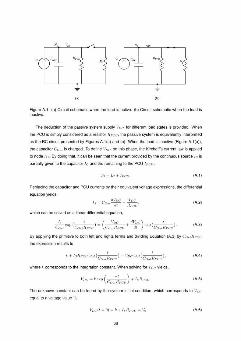
Figure A.1: (a) Circuit schematic when the load is active. (b) Circuit schematic when the load isinactive.
The deduction of the passive system supply VDC for different load states is provided. When
the PCU is simply considered as a resistor RPCU , the passive system is equivalently interpreted
as the RC circuit presented by Figures A.1(a) and (b). When the load is inactive (Figure A.1(a)),
the capacitor COut is charged. To define VDC on this phase, the Kirchoff’s current law is applied
to node N1. By doing that, it can be seen that the current provided by the continuous source IS is
partially given to the capacitor IC and the remaining to the PCU IPCU ,
IS = IC + IPCU . (A.1)
Replacing the capacitor and PCU currents by their equivalent voltage expressions, the differential
equation yields,
IS = COutdVDCdt
+VDCRPCU
, (A.2)
which can be solved as a linear differential equation,
IsCOut
exp( t
COutRPCU
)=
(VDC
COutRPCU+dVDCdt
)exp
( t
COutRPCU
). (A.3)
By applying the primitive to both left and rights terms and dividing Equation (A.3) by COutRPCU
the expression results to
k + ISRPCU exp( t
COutRPCU
)= VDC exp
( t
COutRPCU
), (A.4)
where k corresponds to the integration constant. When solving for VDC yields,
VDC = k exp
(−t
COutRPCU
)+ ISRPCU . (A.5)
The unknown constant can be found by the system initial condition, which corresponds to VDC
equal to a voltage value V0
VDC(t = 0) = k + ISRPCU = V0 (A.6)
68

Doing the required substitution, the voltage supply function during the charge phase is given by
VDC =
(V0 − IsRPCU
)exp
(−t
COutRPCU
)+ IsRPCU , (A.7)
where V0 can be either zero or VOFF depending if VDC expresses the system start-up or a
recharge, respectively. Analysing Equation (A.7), it can be verified that the RPCUCOut term de-
fines the charging time constant. Furthermore, the time independent term ISRPCU corresponds
to the maximum voltage achievable through the capacitor charge. Thus, this term must be higher
than VON so that the load can be activated.
Figure A.1(b) presents the equivalent passive system circuit when the load becomes active.
Following the same procedure used for the inactive load yields
IS = COutdVDCdt
+VDCRPCU
+VDCRL
, (A.8)
which is equivalent to
IS = COutdVDCdt
+VDCRC
, (A.9)
considering RC = RPCU ||RL . As this equation is also a linear differential equation, the discharge
expression is similar to the presented for the charge phase,
VDC =
(V0 − IsRC
)exp
(−t
COutRC
)+ IsRC . (A.10)
Once this is intended to use when the load becomes active, V0 = VON . The conclusions drawn
for the charge expression are also valid for Equation (A.10), however the resistance value is now
given by RC . Through the analysis of the time independent term, ISRC < VOFF for the load to be
deactivated. Furthermore, the overvoltage occurs when ISRC > VLim.
69

BFinal Corners Data
70

−40 −20 0 20 40 60 80 1000
5
10
15
20
Temperature [C]
Pav[nW
]
TypicalSSSNFPFFFNSP
Figure B.1: Average power variation for MOS process corners and temperature range.
−40 −20 0 20 40 60 80 100
0.8
1
1.2
1.4
1.6
1.8
2
Temperature [ C]
VON
[V]
TypicalSSSNFPFFFNSP
Figure B.2: Variation of load activation voltage for MOS process corners and temperature range.
71

−40 −20 0 20 40 60 80 1000.35
0.4
0.45
0.5
0.55
0.6
0.65
0.7
Temperature [ C]
VOFF[V
]
TypicalSSFFFNSP
Figure B.3: Variation of load deactivation voltage for MOS process corners and temperaturerange.
−40 −20 0 20 40 60 80 1000
0.5
1
1.5
2
2.5
3
Temperature [C]
IP[µA]
TypicalSSSNFPFFFNSP
Figure B.4: Variation of current spike value for MOS process corners and temperature range.
−40 −20 0 20 40 60 80 1000,5
1
1,351,5
1,65
2
2,5
Temperature [C]
VLim
[V]
TypicalSSSNFPFFFNSP
Figure B.5: Variation of limiting voltage for MOS process corners and temperature range.
72