power reduction of a cmos high speed.pdf
TRANSCRIPT

FACULDADE DE ENGENHARIA DA UNIVERSIDADE DO PORTO
Power reduction of a CMOS high speedinterface using Clock Gating
Nelson Tiago Lopes Silva
FOR JURY EVALUATION
Mestrado Integrado em Engenharia Eletrotécnica e de Computadores
Supervisor: Eng. Helder Araújo
Second Supervisor: Prof. José Carlos Alves
June 25, 2013

c© Nelson Tiago Lopes Silva, 2013

Resumo
A evolução da consciência do ser humano mudou a forma como olhamos para o mundo em quevivemos. Motivado por questões económicas e ambientais, a palavra "eficiência" tornou-se maisrelevante nas nossas vidas. A industria de semicondutores, especialmente para o domínio digital,tem sido guiada pela necessidade de melhorar a velocidade de processamento e reduzir o custode fabrico de circuitos integrados. Esta foi a tendência antes da explosão dos dispositivos moveisnos últimos anos, que levou a uma corrida por velocidades de relógio mais altas e tamanhos maispequenos. Estas taxas maiores de comutação, maiores correntes de fugas derivadas ao uso dessastecnologias mais pequenas e tensões de threshold mais baixas traduzem-se em maiores consumosde energia que levam a um impacto negativo em algumas métricas de performance ao nível do sis-tema, sendo que a autonomia de dispositivos moveis um dos mais importantes objetivos de designnos dias de hoje. O conceito de "Low Power Design Project" imergiu para, de alguma maneira,resolver este problema. Cientistas e Engenheiros reuniram forças para criar e implementar téc-nicas para serem introduzidas no flow de projeto de sistemas digitais normal. Este trabalho foidesenvolvido em parceria com a Synopsys, uma das líderes mundiais em ferramentas ElectronicDesign Automation e fornecimento de blocos IP (Intellectual Property) digitais e mixed Signal us-ados no projeto, verificação e produção de sistemas eletrónicos digitais, este trabalho enquadra-seno contexto e tem como objetivo o estudo e implementação de uma técnica de design low powerconhecida por Clock Gating, numa interface digital de alta velocidade. Foi importante treinar todoo flow de projeto e ferramentas usadas pela empresa de forma a compreender onde e quando deveser inserido e/ou validado o Clock Gating. Para implementar a inserção automática de Clock Gat-ing, como um dos principais objetivos deste trabalho, foi necessário modificar ligeiramente o flowde projeto standard, e, foi criado, adicionalmente, um método genérico e automático de avaliaçãoprimaria de ganhos de Clock Gating usando scripts desenvolvidos em Python e Cshell. Este pro-cesso de avaliação provou ser determinante para conseguir uma melhor utilização do clock gatinge eficiência. Todo o flow de projeto, apesar de ter sido modificado, foi percorrido e o resultadofoi uma implementação física da interface. Esta implementação, como final e bem caracterizadapor todas as ferramentas de sign-off e bibliotecas de tecnologia, foi analisada usando ferramentasSynopsys dedicadas e especializadas para validar a funcionalidade do circuito e avaliar os ganhosde consumo de energia com base em simulações que consideram operações de funcionamento re-alistas. Finalmente, os resultados foram comparados e avaliados com uma implementação físicada interface sem Clock Gating.
i

ii

Abstract
The evolution of human being consciousness changed the way we look at the world in which welive in. Motivated by economical and environmental issues, the word "efficient" became morerelevant in our daily lives. The semiconductor industry, especially for the digital domain, hasbeen driven by the need to improve the processing speed and reduce the fabrication cost of in-tegrated circuits. This was the trend before the explosion of mobile devices through the recentyears gone by, which led to a race for higher clock speeds and smaller feature sizes. These highercommutation ratios, higher leakage power derived from the use of these smaller technologies andlower threshold voltages translates in higher power consumption, which impacts negatively inseveral performance metrics at the system level, being the autonomy of mobile devices one of themost important design goals nowadays. The concept of "Low Power Design Project" emerged to,somehow, solve this problem. Scientists and Engineers gathered forces to create and implementtechniques to be introduced in the normal Digital Systems Design Flow. This work was developedin partnership with Synopsys, one of the world’s leader in Electronic Design Automated Toolsand provider of digital and mixed signal IP (Intellectual Property) blocks used in the design, ver-ification and manufacturing of electronic systems digital, this work fits in this context, and aimsto study and implement a low power design technique known by Clock Gating, in a high speeddigital interface. It was important to practice with the Project Flow and Tools used in the Companyin order to understand where and when Clock Gating must be inserted and/or validated. To im-plement automatic Clock Gating insertion as one of the main goals of this work, it was necessaryto slightly modify the standard Project Flow, and, additionally was created a generic automaticfirst evaluation of Clock Gating gains using scripts developed Python and Cshell. This evaluationprocess proved to be decisive to achieve better clock gating usage and efficiency. All the ProjectFlow, even modified, was ran and the result were a physical implementation of the interface. Thisimplementation, as a final and well characterized implementation by all sign-off tools and technol-ogy libraries, was analysed using dedicated and specialized Synopsys tools to validate the circuitfunctionality and evaluate the power consumption gains based on simulations considering realisticoperating conditions. Finally, the results were confronted and evaluated with a non Clock Gatinginterface physical implementation.
iii

iv

Acknowledgements
I would like to thank all Synopsys Engineers but especially, my restless colleagues, Eng. SergioCosta and Eng. João Cacheiro. I would like to thank also to you, no less important, my SupervisorsEng. Helder Araújo and Prof. José Carlos Alves, Eng. Mara Campos, Eng. Rocha and Eng. LuisCruz. Lastly, I wish to express my deepest gratitude and warmest appreciation to my mother AnaLopes, sister Ana Silva and girlfriend Joana Sousa. I’m truly thankful to all of your irreplaceablesupport. Thank you so much.
Nelson Tiago Lopes Silva
v

vi

“I do the very best I know how - the very best I can;and I mean to keep on doing so until the end.”
Abraham Lincoln
vii

viii

Contents
Resumo i
Abstract iii
1 Introduction 11.1 Motivation . . . . . . . . . . . . . . . . . . . . . . . . . . . . . . . . . . . . . . 11.2 Goals . . . . . . . . . . . . . . . . . . . . . . . . . . . . . . . . . . . . . . . . 21.3 Document Structure . . . . . . . . . . . . . . . . . . . . . . . . . . . . . . . . . 2
2 State of the Art 32.1 Introduction . . . . . . . . . . . . . . . . . . . . . . . . . . . . . . . . . . . . . 32.2 Static and Dynamic Power . . . . . . . . . . . . . . . . . . . . . . . . . . . . . 4
2.2.1 Static Power . . . . . . . . . . . . . . . . . . . . . . . . . . . . . . . . 52.2.2 Dynamic Power . . . . . . . . . . . . . . . . . . . . . . . . . . . . . . . 5
2.3 Clock Gating . . . . . . . . . . . . . . . . . . . . . . . . . . . . . . . . . . . . 62.3.1 Glitch . . . . . . . . . . . . . . . . . . . . . . . . . . . . . . . . . . . . 82.3.2 Clock Skew . . . . . . . . . . . . . . . . . . . . . . . . . . . . . . . . . 10
2.4 The Case Study Circuit: A High-Speed Digital Interface . . . . . . . . . . . . . 122.5 Synopsys EDA Tools . . . . . . . . . . . . . . . . . . . . . . . . . . . . . . . . 13
3 Digital Design Flow 153.1 Introduction . . . . . . . . . . . . . . . . . . . . . . . . . . . . . . . . . . . . . 153.2 From an Idea to a Model . . . . . . . . . . . . . . . . . . . . . . . . . . . . . . 153.3 Logic Synthesis . . . . . . . . . . . . . . . . . . . . . . . . . . . . . . . . . . . 163.4 Post-Synthesis Verification . . . . . . . . . . . . . . . . . . . . . . . . . . . . . 183.5 Physical Implementation . . . . . . . . . . . . . . . . . . . . . . . . . . . . . . 19
3.5.1 Floorplan . . . . . . . . . . . . . . . . . . . . . . . . . . . . . . . . . . 193.5.2 Placement . . . . . . . . . . . . . . . . . . . . . . . . . . . . . . . . . . 203.5.3 Clock Tree Synthesis . . . . . . . . . . . . . . . . . . . . . . . . . . . . 213.5.4 Routing . . . . . . . . . . . . . . . . . . . . . . . . . . . . . . . . . . . 22
3.6 Parasitic Extraction . . . . . . . . . . . . . . . . . . . . . . . . . . . . . . . . . 233.7 Timing and Power Analysis . . . . . . . . . . . . . . . . . . . . . . . . . . . . . 233.8 DRC and LVS . . . . . . . . . . . . . . . . . . . . . . . . . . . . . . . . . . . . 233.9 Manufacture and Test . . . . . . . . . . . . . . . . . . . . . . . . . . . . . . . . 24
4 Automatic Clock Gating Insertion 254.1 Introduction . . . . . . . . . . . . . . . . . . . . . . . . . . . . . . . . . . . . . 254.2 Clock Gating Insertion . . . . . . . . . . . . . . . . . . . . . . . . . . . . . . . 254.3 Validation . . . . . . . . . . . . . . . . . . . . . . . . . . . . . . . . . . . . . . 29
ix

x CONTENTS
4.4 Physical Implementation . . . . . . . . . . . . . . . . . . . . . . . . . . . . . . 294.5 Power Analysis . . . . . . . . . . . . . . . . . . . . . . . . . . . . . . . . . . . 294.6 Automatic Evaluation of Clock Gating Gains . . . . . . . . . . . . . . . . . . . 29
4.6.1 Implementation . . . . . . . . . . . . . . . . . . . . . . . . . . . . . . . 30
5 Final Results 335.1 Introduction . . . . . . . . . . . . . . . . . . . . . . . . . . . . . . . . . . . . . 335.2 First Approach . . . . . . . . . . . . . . . . . . . . . . . . . . . . . . . . . . . 335.3 Top Level Insertion . . . . . . . . . . . . . . . . . . . . . . . . . . . . . . . . . 355.4 Physical Implementation . . . . . . . . . . . . . . . . . . . . . . . . . . . . . . 375.5 Power Analysis . . . . . . . . . . . . . . . . . . . . . . . . . . . . . . . . . . . 38
6 Conclusion 416.1 Overall Results . . . . . . . . . . . . . . . . . . . . . . . . . . . . . . . . . . . 416.2 Future Work Proposal . . . . . . . . . . . . . . . . . . . . . . . . . . . . . . . . 41
A Automatic Evaluation of Clock Gating Gains - Source Code 43A.1 runCG_EVAL Source Code . . . . . . . . . . . . . . . . . . . . . . . . . . . . . 43A.2 cg_eval1.py Source Code . . . . . . . . . . . . . . . . . . . . . . . . . . . . . . 44A.3 cg_eval2.py Source Code . . . . . . . . . . . . . . . . . . . . . . . . . . . . . . 45A.4 cg_eval3.py Source Code . . . . . . . . . . . . . . . . . . . . . . . . . . . . . . 47
References 51

List of Figures
2.1 Moore’s Law . . . . . . . . . . . . . . . . . . . . . . . . . . . . . . . . . . . . 32.2 Leakage paths in a CMOS inverter . . . . . . . . . . . . . . . . . . . . . . . . . 52.3 Charge and discharge of capacitive output load in CMOS inverter . . . . . . . . . 62.4 Short circuit power in CMOS inverter . . . . . . . . . . . . . . . . . . . . . . . 72.5 Basic implementation of Clock Gating . . . . . . . . . . . . . . . . . . . . . . . 72.6 Register-AND clock gating implementation . . . . . . . . . . . . . . . . . . . . 82.7 Setup and hold time . . . . . . . . . . . . . . . . . . . . . . . . . . . . . . . . . 92.8 Glitch on a AND clock gating implementation . . . . . . . . . . . . . . . . . . . 92.9 AND-Latch clock gating implementation . . . . . . . . . . . . . . . . . . . . . 102.10 Clock tree . . . . . . . . . . . . . . . . . . . . . . . . . . . . . . . . . . . . . . 112.11 Skew example . . . . . . . . . . . . . . . . . . . . . . . . . . . . . . . . . . . . 122.12 High speed interface architecture . . . . . . . . . . . . . . . . . . . . . . . . . . 13
3.1 Digital Design Flowchart . . . . . . . . . . . . . . . . . . . . . . . . . . . . . . 163.2 Logic synthesis overview . . . . . . . . . . . . . . . . . . . . . . . . . . . . . . 173.3 Floorplan example (Adapted figure)[1] . . . . . . . . . . . . . . . . . . . . . . . 203.4 Placement example(zoomed-in image)[2] . . . . . . . . . . . . . . . . . . . . . 213.5 Clock tree example (Adapted figure)[2] . . . . . . . . . . . . . . . . . . . . . . 22
4.1 Synchronous load-enable register with multiplexer . . . . . . . . . . . . . . . . 254.2 Clock Gating report from Design Compiler R© . . . . . . . . . . . . . . . . . . . 284.3 Automatic evaluation of clock gating gains flowchart . . . . . . . . . . . . . . . 30
5.1 Graphic illustration of the clock gating coverage in the designs . . . . . . . . . . 35
xi

xii LIST OF FIGURES

List of Tables
5.1 Control block clock gating summary . . . . . . . . . . . . . . . . . . . . . . . . 335.2 Control block area report . . . . . . . . . . . . . . . . . . . . . . . . . . . . . . 345.3 Control block power report with 30% input switching activity . . . . . . . . . . . 345.4 Control block power report with 50% input switching activity . . . . . . . . . . . 345.5 High speed interface clock gating summary . . . . . . . . . . . . . . . . . . . . 355.6 Clock gating coverage in the designs . . . . . . . . . . . . . . . . . . . . . . . . 365.7 High speed interface clock gating summary with automatic evaluation . . . . . . 375.8 High speed interface area report . . . . . . . . . . . . . . . . . . . . . . . . . . 375.9 Library cell usage . . . . . . . . . . . . . . . . . . . . . . . . . . . . . . . . . . 385.10 Power consumption in Hibernate mode . . . . . . . . . . . . . . . . . . . . . . . 385.11 Power consumption in Sleep mode . . . . . . . . . . . . . . . . . . . . . . . . . 395.12 Power consumption in HighSpeed1 mode . . . . . . . . . . . . . . . . . . . . . 395.13 Power consumption in HighSpeed2 mode . . . . . . . . . . . . . . . . . . . . . 40
xiii

xiv LIST OF TABLES

Abbreviations
ASIC Application-Specific Integrated CircuitCGE Clock Gating EfficiencyCMOS Complementary Metal-Oxide-SemiconductorCTS Clock Tree SynthesisDRC Design Rule CheckingEC Equivalence CheckingECO Engineering Change OrderEDA Electronic Design AutomationFPGA Field-Programmable Gate ArrayGDS Graphic Database SystemGTECH GeneralHDL Hardware Description LanguageIC Integrated CircuitIP Intellectual PropertyLVS Layout versus SchematicNMOS N-type Metal-Oxide-SemiconductorNTB Native TestBenchPMOS P-type Metal-Oxide-SemiconductorRC Resistor–CapacitorRTL Register Transfer LevelSAIF Switching Activity Interchange FormatVCD Value Change DumpVCS Verilog Compiler SimulatorVLSI Very Large Scale Integration
xv


Chapter 1
Introduction
1.1 Motivation
Since the early times, human beings have always had a need for communication. In the last
century, technology has evolved to provide better and better communication systems that in general
make life easier for the human population. Over the recent decades, an explosion of devices and
services has evolved, which have shown an increase in faster, and more reliable increase in our
communication systems. This was only possible due to the fact that mobile electronic devices
became more powerful, with the increase of computation capability and the improvements of
the communications in speed and reliability. But all these improvements have cost. One of the
most concerning cost is the power consumption. Inserting larger and more efficient batteries was
the solution in the latest years as long as they did not compromise mobility. In modern days,
economical and environmental issues force us to think about other solutions such as techniques
to reduce the power consumption in digital systems. This work was developed in partnership
with Synopsys and aims to study, practice and evaluate a digital design technique for CMOS low
power consumption systems called "clock gating". This was exercised in a current design of a high
speed digital interface, selected as a case study, and the design flow was performed with Synopsys
EDA tools and technology libraries currently used for mature products. Clock gating, as the name
suggests, consists in disabling the clock signal that feeds sequential blocks, when their registers are
not being updated. This enables reducing the switching activity responsible by an important part of
the overall power consumption, due to the charge/discharge of the load capacitance, the so called
dynamic power. The implementation of this technique involves the introduction of additional logic
to gate the clock. Since this technique is used to decrease the switching activity, is expected to
get great results in the digital interface due his high frequency operation and large amount of
sequential logic. It is vitally important to mention that this work was a great opportunity to face
and deal with a business environment, cutting edge technologies and state of the art EDA tools
while integrated in a design team of one of the world’s leaders in EDA tools and IP (Intellectual
Property) provider.
1

2 Introduction
1.2 Goals
This work was proposed by Synopsys, one of the worlds leader in electronic design automation
tools and provider of digital blocks and mixed signal used in the design, verification and manufac-
ture of electronic systems digital. The main goals initially proposed were:
• Study, understand and practice with the design flow used in the company;
• Understand the interface architecture and main operating modes;
• Study the technique of clock gating;
• Implement automatic clock gating insertion and travel trough all the design flow;
• Design validation using test-bench simulations, formal verifications, design rule check and
layout versus schematic verifications;
• Analyse the results of area occupation, gate-count and power savings of the final physical
implementation of the interface.
• Compare the results with the physical implementation of the non clock gated interface;
Some additional goals were established during the project:
• Create an automatic process to evaluate the clock gating insertion gains before synthesis
using the target library;
• Based on the last report, elaborate a Tcl script that removes the clock gating insertion of
registers with lower gains.
1.3 Document Structure
Besides this first chapter introducing the subject and the motivation for this work, the dissertation
is organized in the next six chapters. Chapter 2 presents the state of the art where all important
concepts and definitions will be explained in order to subserve a better understanding of the theme.
In Chapter 3, an overview of the complete design flow in use in the company is presented along
with all the tools used in each step. The automatic clock gating insertion is discussed in Chapter
4, along with the modifications proposed to the current design flow in order to integrate this tech-
nique. Chapter 4 also presents the methodology created using Python and Cshell scripts for the
automatic evaluation of clock gating gains. The final evaluation results are presented and discussed
in Chapter 5, applied to a digital block of a high-speed digital communications interface that has
been elected as a case study for this work. Finally, Chapter 6 concludes this work and provides
suggestions for future developments in the framework of this subject with particular emphasis in
the benefits resulting from a power aware design flow from the industrial point of view.

Chapter 2
State of the Art
2.1 Introduction
In 1965, Gordon Moore, Intel’s Co-Founder, predicted that the number of transistors in a chip
would double every two years. This prediction was called "Moore’s Law" (Figure 2.1) and has
been verified since then. The first Intel’s processor was launched in 1971, the Intel 4004. He
had 2300 transistors using 10µm technology, [3] nowadays there is integrated circuits with about
seven billion transistors using 28nm. This record was achieved by Xilinx [4].
Figure 2.1: Moore’s Law
3

4 State of the Art
In the early days of the investigation of microelectronics and integrated circuits the main chal-
lenges were timing closure and area minimization, and there was no other concern to be prioritized.
All EDA tools used in IC industry were designed to work with this guidance, either maximizing
the speed (clock frequency) and minimizing area, and power consumption issues were ignored
because they were irrelevant given the use of CMOS technologies [5]. At that time, CMOS was
considered a low power technology for the clock frequencies in use. However, due to continu-
ing miniaturization of very large scale integrated (VLSI) circuits and the great increase of clock
frequencies, the CMOS technology once considered a low power technology showed huge power
consumption in these conditions. Some other facts motivated this worsening such the use of lower
transistors threshold voltages and supply voltages. Power has become as important as timing or
area due to having exceeded acceptable values. The increasing power consumption raised other
issues, the excessively high temperatures that devices can reach which leads to higher costs in ce-
ramic packaging, instead of regular plastic packaging and additional cooling systems required for
normal system operation. Higher operating temperatures of silicon devices also reduces reliability,
because its electrical characteristics frequently undergo intermittent or permanent changes. The
mobility of portable devices such as cellphones and laptops has been affected by the increase of
power consumption of IC devices. The introduction of larger and heavier batteries has compro-
mised that fact. Power consumption also has become an increasing and concerning challenge by
economical and environmental issues. The cost of electrical energy substantially increased, moti-
vated by the constant growing of high power consumer computers, servers, and electronic devices
that are constantly connected to the power grid and their cooling systems. It is noticeable that a
small decrease of power consumption in an electronic device used in large scale can result in large
cost savings to users and significant benefits to the environment as well.
2.2 Static and Dynamic Power
The electric power consumption in CMOS digital circuits can be represented by the sum of two
components: static power consumption and dynamic power consumption [6], [7]:
Ptotal = Pstatic+Pdynamic (2.1)
Dynamic power is consumed in every single switch of transistors operating mode. This type of
power only depends on the clock frequency and switching activity of the circuit. Static power is
power related to the leakage current that flows through the transistor while it is powered, so it is
not dependent of the clock frequency or its switching activity.

2.2 Static and Dynamic Power 5
2.2.1 Static Power
As the feature size of recent CMOS digital technologies is getting smaller, static power, also re-
ferred as leakage power, is becoming increasingly significant. This power is technology dependent
and is proportional to the number of transistors in the circuit. In deep-submicron processes, the
static power reaches similar values to dynamic power. The relevant causes of the leakage power
are p-n junction diode leakage from n-well when CMOS is tied low, p-n junction diode leakage to
substrate when CMOS is tied high, gate leakage and sub-threshold leakage. The Figure 2.2 shows
these leakage paths in a CMOS inverter.
Figure 2.2: Leakage paths in a CMOS inverter
2.2.2 Dynamic Power
Dynamic power is consumed in logic transitions in nets and can be divided in two components,
switching power and short circuit power.
Pdynamic = Pswitch+Pshort (2.2)
Switching power is energy consumed by the charging and discharging of internal parasitic capac-
itive loads and external capacitive loads at the output of the cell. It only depends on the switching
activity, supply voltage and the capacitive loads. The switching power can be expressed using the
following mathematical expression:
Pswitch = α ×CL×V dd2 × f clk (2.3)

6 State of the Art
Considering:
• α - Switching activity factor
• CL - Capacitive load
• V dd - Supply voltage
• f clk - Clock frequency
The mathematical expression reveals that Vdd is a squared term. The usage of lower supply
voltages or multi-voltage designs methodologies will cause a greater impact on dynamic power
reduction taking advantage of this fact.
As we can see in Figure 2.3, the transition from logic level 0 to 1 in the output of the CMOS
inverter charges the capacitive load of the output net through the PMOS and transition from logic
level 0 to 1 discharges the same capacitive load but now through NMOS.
Figure 2.3: Charge and discharge of capacitive output load in CMOS inverter
Short circuit power is the consequence of the short-circuit current that flows through the the
pair PMOS and NMOS from VSS to ground when both are in active mode at the time of transition.
The amount of current that flows under these circumstances depends on the switching activity and
the time that transistors take to switch. The use of lower threshold voltages results in additional
short circuit power consumption because the transistor switches for active mode faster, increasing
the amount of time that both are active simultaneously. The Figure 2.4 illustrates this effect.
2.3 Clock Gating
There are some low power design strategies to reduce power consumption that strikes directly on
the Dynamic and Static power dependencies. For example, multi-voltage , multi-clock, multi-
Vt, supply voltage reduction or even power gating. Clock gating is a technique that reduces the
switching activity of sequential elements of the circuit, leading to a decreased dynamic power
2.3 Clock Gating 7
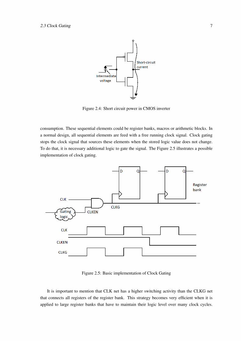
Figure 2.4: Short circuit power in CMOS inverter
consumption. These sequential elements could be register banks, macros or arithmetic blocks. In
a normal design, all sequential elements are feed with a free running clock signal. Clock gating
stops the clock signal that sources these elements when the stored logic value does not change.
To do that, it is necessary additional logic to gate the signal. The Figure 2.5 illustrates a possible
implementation of clock gating.
Figure 2.5: Basic implementation of Clock Gating
It is important to mention that CLK net has a higher switching activity than the CLKG net
that connects all registers of the register bank. This strategy becomes very efficient when it is
applied to large register banks that have to maintain their logic level over many clock cycles.

8 State of the Art
There is metric used to evaluate the efficiency of the technique called Clock Gating Efficiency
(CGE) which represents the amount of time that each register is off compared to the total run time
[8]. Clock gating could be implemented using a unique gate AND or a more complex structure
with latch/register and gates.
Figure 2.6: Register-AND clock gating implementation
The first option is very simple to implement but a problem arises, the Glitch. Latch based
clock gating implementations are Glitch free but you have to use more area. The implementation
of clock gating implies additional time constraints to the project and other problems such as clock
skew.
2.3.1 Glitch
In electronics, a Glitch is an undesired transition that occurs before the signal settles to its intended
value. This can happen when certain timing considerations of the design are not met. For example,
the flip-flop, or latch has two important timing considerations for its normal functionality, setup
time and hold time [9]. Setup time is the minimum amount of time the data signal should be held
steady before the clock event so that the data is reliably sampled by the clock. Hold time is the
minimum amount of time the data signal should be held steady after the clock event so that the
data is reliably sampled as it is demonstrated in Figure 2.7.

2.3 Clock Gating 9
Figure 2.7: Setup and hold time
In the Figure 2.8 is illustrated a possible Glitch using a simple AND implementation of clock
gating.
Figure 2.8: Glitch on a AND clock gating implementation

10 State of the Art
As it was mentioned before, there is other implementations of clock gating using a more
complex structure. In the following Figure 2.9 we could see that the synchronous latch of the
clock gate structure prevents possible Glitches.
Figure 2.9: AND-Latch clock gating implementation
2.3.2 Clock Skew
As discussed, the implementation of clock gating in synchronous circuits implies the insertion of
additional logic over the clock network. One of the many problems that a designer faces is the
clock tree construction and balancing. The clock tree is the network that sources all the sequential
components in a certain clock domain.

2.3 Clock Gating 11
Figure 2.10: Clock tree
This additional logic will interfere in that process leading to a problem called clock skew. The
clock skew is the difference in the arrival time of the clock pulse between two sequentially-adjacent
registers and can be expressed mathematically using the following expression[9]:
Tskewi, j = tRi − tR j (2.4)
Considering:
• Ri and R j - two sequentially-adjacent registers
• tRi - the arrival time of Register i
• tR j - the arrival time of Register j
In Figure 2.11 we can visualize this effect.

12 State of the Art
Figure 2.11: Skew example
Skew is caused mainly by different behaviour of the components given temperature variations,
wire-interconnect length or material imperfections. Clock skew was always seen as a problem
because it could cause hold or setup violations in the registers, but in fact, can also benefit a circuit
by increasing the clock period locally giving more slack to the designer to solve some critical
paths.
2.4 The Case Study Circuit: A High-Speed Digital Interface
The host design team at Synopsys considered interesting the use of a high-speed interface to im-
plement and validate all the automatic clock gating insertion process, due its clocking architecture
and operating modes. This interface has several clocks with frequency values from 3MHz to
600MHz. There is a low power mode that puts the interface in idle and is also used to do all
interface configurations. There is also a low speed mode and a high speed mode for data transfer
purposes, each one can operate in three different transfer speeds. The interface architecture is
composed by a finite state machine that controls the interface, configuration registers, a low speed
data path, a high speed data path and logic for testability. The existing design of this interface
already included basic implementation of clock gating introduced manually at RTL level in order
to gate the clocks that are not in use while a specific mode is operating, however, it is expected
to achieve better results with the implementation under study. It is important to mention that this
high-speed interface was already implemented in 28nm technology.

2.5 Synopsys EDA Tools 13
Figure 2.12: High speed interface architecture
One of the main challenges of clock gating is finding the best places to use it. After an in-depth
study of the interface we could approve how interesting it really is by the following characteristics:
• The interface contains a large configuration register bank (nearly 39% of the total number of
registers) which are used only in the initiation of the interface or when the operating mode
is changed.
• When a specific mode is operating, most of the rest of the logic responsible to the other
modes are not in use.
• The interface uses relatively high clock frequencies.
All these aspects support the idea of achieving excellent results in this interface with the auto-
matic clock gating insertion.
2.5 Synopsys EDA Tools
Synopsys has developed a set of electronic design automated tools to support the whole standard
design flow. These tools are recognized as a reference and "signoff quality" by the chip design
community. In this work we used the following tools for the specified purposes:
• Design Compiler R©: It is a family of tools used for RTL synthesis, synthesis optimization
and test. Design Complier include two important features:
– Formality R©: It is an equivalence-checking (EC) tool that uses formal, static tech-
niques to determine if two versions of a design are functionally equivalent.
– Power CompilerTM: It is used for power consumption optimization at the RTL and gate
level, and enables other concurrent timing, area, power and test optimizations within
the Design Compiler R© synthesis solution.

14 State of the Art
• IC Compiler: It is a tool used for synthesis, low-power design, and design for manufactura-
bility. It is also used for physical implementation which includes flat and hierarchical design
planning, placement and optimization, clock tree synthesis, routing, manufacturability, and
low-power capabilities.
• PrimeTime R©: It is a tool for crosstalk timing, noise, power (Prime Power R© feature) and
statistic time analysis.
• StarRCTM: It is the EDA industry’s gold standard for parasitic extraction for gate-level and
transistor-level digital and custom IC designs.
• HerculesTM: It is a DRC (Design Rule Checking) and LVS (Layout versus Schematic) veri-
fication tool.
• Synopsys VCS R©: It is a functional verification tool that provides high performance simula-
tion engines, constraint solver engines, native testbench (NTB) support, broad SystemVer-
ilog support, verification planning, coverage analysis and closure, and an integrated debug
environment.
Chapter 3 will describe in detail where and when this tools are used in the project flow, their
capabilities and how they work.
Chapter 3
Digital Design Flow
3.1 Introduction
In the early days of the digital systems, projects were difficult and time consuming. It was nec-
essary to create a well-defined design flow in order to make this process faster and, somehow, to
fight against the growing complexity of digital systems. This design flow became standard and all
IC related industries use it. It is an overall view of the IC conception process with a guide line that
starts from the idea of a functionality to his final physical test.
The flow chart present in Figure 3.1 illustrates all steps of the standard design flow. In the
following sections we find a brief description of the design flow and the tools used to support the
work.
3.2 From an Idea to a Model
The conception of a digital system is born from a need, an idea or an issue. The system func-
tionality will be a mapped digital solution. It is important to question the feasibility of the
idea like production costs, development time, implementation target (ASIC, FPGA, MicroCon-
troller/MicroProcessors, CPU or off-the-shelf based circuits). After all this issues settled, we
should divide the solution in small step solutions to easily create each functional specification, and
in turn, develop synthesizable models in HDL (VHDL or Verilog) that could also be reused. Such
models usually define a clear separation between control parts, such as finite state machines, and
operative parts like arithmetic and logic units. Each model should be verified and tested through
the creation of testbenches and further simulation to grant correct functional behaviour. It is ad-
visable that the creation of testbenches should not be made by the same person who created the
models to prevent and avoid possible human errors. With all models gathered and the system in-
tegration already made, it is mandatory to do additional simulations in this new context. If any of
the steps can’t be accomplished successfully by system errors or limitations it is possible to step
back to modify or even restructure the models as the back flow arrows suggest.
15

16 Digital Design Flow
Figure 3.1: Digital Design Flowchart
3.3 Logic Synthesis
In this work, the steps mentioned before were not preformed. This is our starting point, a high-
speed digital interface described in synthesizable Verilog blocks, fully tested and validated. Logic
synthesis is a translation from an RTL description to a possible gate-level realization that meets
user-defined constraints such as area, timings or power consumption and using a unique or a set
of technology libraries.
The targeted logic gates belong to a library that is provided by a foundry or an IP company
as part of a so-called design kit. Typical gate libraries include hundreds of combinational and
sequential logic gates with different driving strengths. Logic functions are implemented using the
very same gates. The gate library is described in a tool-specific format that defines, for each gate,
its function, area, timing and power characteristics and environmental constraints.
To perform the logic synthesis was used Synopsys Design Compiler R©. It is important to make
a previous setup where is specified mandatory variables such as target_library, synthetic_library,
link_library and symbol_library [10]. The target library variable defines the technology library
that Design Compiler R© uses to build the circuit. That is, during technology mapping phase Design

3.3 Logic Synthesis 17
Figure 3.2: Logic synthesis overview
Compiler R© selects components from the library specified with the target library variable to build
the gate-level netlist. The synthetic library variable specifies the synthetic or DesignWare libraries.
These synthetic libraries are technology-independent, microarchitecture-level design libraries pro-
viding implementations for various IP blocks. The link library variable is used to resolve design
references in order to connect all the library components and designs its references. Symbol li-
brary defines the schematic symbols for components in technology library that will be used for
drawing design schematics.
The logic synthesis using Design Compiler R© is composed by the following main steps: read
in the design, set the constraints, optimize the design, analyse the results and save the design
database [10].
The first step is to read the HDL design into Design Compilers memory. This step is divided
in two separated tasks:
• Analyse (performed by the command analyze) - This command reads the HDL description,
checks it for syntactical errors and creates HDL library objects in an HDL-independent
intermediate format.
• Elaborate (performed by the command elaborate) - This command translates the design into
a technology-independent design (GTECH - Generic technology), translates the arithmetic
operators into DesignWare components and resolves design references.
At the end of this process the design is represented in GTECH format, which is an internal,
equation-based, technology-independent design format.
The next step is set design constrains. These constrains will define what Design Compiler R©can or cannot do with the design or how it behaves. We can define design rule constraints (e.g.

18 Digital Design Flow
maximum transition time, maximum fanout, maximum and minimum capacitance) and optimiza-
tion constraints (e.g. input and output delays, minimum and maximum path delays, clock fre-
quency and clock delays). Design Compiler R© always tries to meet both constraints but gives
priority to design rule constraints over optimization constraints.
We also must define the design environment to model the conditions in which the design is
supposed to operate. The design environment is defined by operating conditions (e.g. temperature,
process and voltage) and a wire load model, used to calculate the effect of interconnect nets in
capacitance, resistance and area.
Next, through the command compile, Design Compiler R© performs three main optimiza-
tions [10]:
• Architectural optimizations, that includes arithmetic optimizations using the rules of algebra
to improve the implementation of the design, resource sharing to reduce the amount of
hardware and selection of different Designware implementations.
• Logic-level optimizations, that consists in structuring optimization which evaluates the de-
sign equations and tries to optimize using Boolean algebra, and flattening optimization to
produce faster logic by minimizing the levels of logic between the inputs and outputs.
• Gate-level optimizations, that performs the mapping process from technology-independent
netlist (GTECH) to the cells specified by the target_library variable, delay optimizations to
fix the the timing violations introduced by mapping process, design rule fixing that inserts
buffers or resizes existing cells to fix design rule violations, and area optimizations.
Once the synthesis has been completed it is important to analyse the results and verify that
the design meets the goals set by the constraints. It is possible to identify the possible causes of a
certain unmet goal analysing the reports. To complete the process we have to save the result in a
database format or a gate-level netlist format.
3.4 Post-Synthesis Verification
To verify that the synthesis was done correctly without modifying the circuit, it is important to sim-
ulate the netlist or perform formal a verification between the RTL code and the resulting netlist.
The first option is very time consuming because netlist simulation could take hours or even days
that will also interfere in debuging. Synopsys developed a great tool known as Formality R© that is
capable to make formal verifications between a reference desing in RTL or netlist and an imple-
mentation design in netlist. By formally comparing a reference RTL design or a netlist to another
netlist resulting from the synthesis process, the designer can determine whether the implementa-
tion is functionally equivalent to the reference design. This process is divided in four main steps:
3.5 Physical Implementation 19
• Specify the reference design
• Specify the implementation design
• Run the verification (match and veri f y)
• Analyse reports of matched and unmatched points
If the formal verification fails the designer must identify the problem, correct it and perform a
new synthesis with the convenient modifications.
3.5 Physical Implementation
Physical implementation, also called physical synthesis, is a process that generates a new modified
netlist and a corresponding layout that satisfies timing, area, power, and routability. Physical
synthesis starts by the floorplanning, followed by placement, clock tree synthesis and finally, route.
Nowadays, designers have to consider that these steps are very interdependent. Synopsys has
created a unique tool named IC Compiler to embrace this fundamental part of the IC backend
design process in order to achieve better and consistent results.
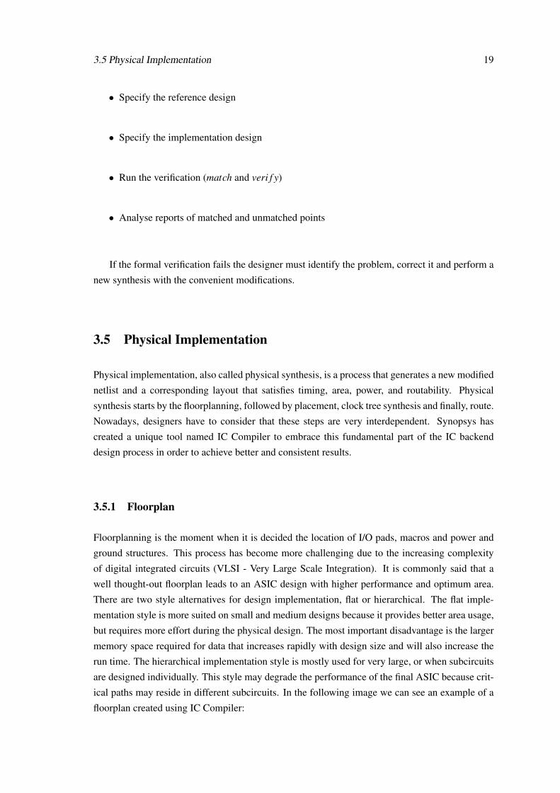
3.5.1 Floorplan
Floorplanning is the moment when it is decided the location of I/O pads, macros and power and
ground structures. This process has become more challenging due to the increasing complexity
of digital integrated circuits (VLSI - Very Large Scale Integration). It is commonly said that a
well thought-out floorplan leads to an ASIC design with higher performance and optimum area.
There are two style alternatives for design implementation, flat or hierarchical. The flat imple-
mentation style is more suited on small and medium designs because it provides better area usage,
but requires more effort during the physical design. The most important disadvantage is the larger
memory space required for data that increases rapidly with design size and will also increase the
run time. The hierarchical implementation style is mostly used for very large, or when subcircuits
are designed individually. This style may degrade the performance of the final ASIC because crit-
ical paths may reside in different subcircuits. In the following image we can see an example of a
floorplan created using IC Compiler:

20 Digital Design Flow
Figure 3.3: Floorplan example (Adapted figure)[1]
3.5.2 Placement
In this step we place all the cells from the netlist extracted from the synthesis and some other
important cells such as endcaps, antenna diodes and dummycells over the floor (silicon surface).
Endcap cells are placed at the end of cellrows to connect power and ground rails and to ensure gaps
do not occur between well or implant layers which could cause design rule violations. Antenna
diodes are used to prevent the excess of charge on a huge single metal nets that could damage
connected transistors in manufacturing process. Dummycells are random cells from target library
that could be used for future metal ECO purposes (Engineering Change Orders) in order to reduce
the costs of layer modification. In IC Compiler we must:
• Create one empty physical library (create_mw_lib)
• Load the netlist previously extracted from synthesis (read_verilog)
• Create the power connection from the standard cell power pins to the design power supplies
(pg_connect)
• Load the TLU+ files which informs the tool about parasitic effects between nets and cells
(load_tlup)
• Load the floorplan definitions
• Insert the cells in the floorplan in order to meet timing constraints but not avoiding overlap-
ping cells (create_placement)

3.5 Physical Implementation 21
• Legalize the placement to solve overlapping problems by moving overlapped cells for the
nearest free space (legalize_placement)
When he tool inserts the cells and legalizes the placement, it also performs different optimiza-
tions such as, area, congestion or timing. At this moment the cells aren’t physically connected,
however, we already have a notion of possible critical paths and congestion areas defined by virtual
connections. Its important, at this phase, to optimize all the placement. To force that, designers
always use more demanding constraints. In Figure 3.4 we can see an example of a placement in
IC Compiler:
Figure 3.4: Placement example(zoomed-in image)[2]
3.5.3 Clock Tree Synthesis
In the clock tree synthesis it is created a balanced buffer tree that sources the clock signal to all
registers in each clock domain. In the beginning, the clock signal has a huge fanout, which means
that it is connected to all registers using it. This raises some problems such as, setup, hold and
transition time violations due to unacceptable high load capacitances of all the clock destinations.
There are also clocks that are generated from input clocks. The buffer tree will solve this problem
dividing the fanout to the buffers in the leafs of the tree as we can observe in Figure 3.5.
There are some cautions to be attended. The implementation of a clock tree will cause clock
skew, a problem already explained in Chapter 2.3.2. In IC Compiler we could perform the the
Clock Tree Syntesis (CTS) using the command create_cts_clocks.

22 Digital Design Flow
Figure 3.5: Clock tree example (Adapted figure)[2]
3.5.4 Routing
At this moment we have a floorplan with all cells inserted and a clock tree already implemented and
connected to all sequential cells. The routing is responsible to design the wires used to connect all
cells of the circuit. The wires are designed using metal layers and consecutive layers are connected
through vias. Routing introduces RC parasitic effects that impacts negatively on timing, transition
and capacitance slacks.
In IC Compiler, routing is made in three different steps:
• Global Routing: In this step, the tool will design the best routing nets
• Track Assignment: The tools defines and assign nets to a specific metal layers
• Search & Repair: IC Compiler tries to fix violations that could appear on the previous steps
At the end of this process we have a post-layout netlist and a GDSII that describes our physical
implementation of the circuit. GDSII is a standard database file format used for data exchange of
integrated circuit or IC layout artwork.

3.6 Parasitic Extraction 23
3.6 Parasitic Extraction
In early integrated circuits, the impact of the wiring was negligible, and wires were not considered
as electrical elements of the circuit. However, below the 0.5µm technology node resistance and
capacitance of the interconnects started making a significant impact in circuit performance. This
impact is calculated using appropriated tools such as StarRCTM. This tool performs parasitic
extraction used to create an accurate analog model of the circuit. With this information we could
perform detailed simulations that can emulate actual digital and analog circuit responses in order
to verify timing and circuit functionality.
3.7 Timing and Power Analysis
As mentioned before, the parasitics extraction has a negative impact on the modern circuits. This
effect could modify dramatically the circuits behaviour. To measure this impact and detect possible
issues, it is important to perform timing analysis. Synopsys developed an excellent tool for this
purpose. It is also important to analyse the chip power consumption, electro-migration and IR drop
before sending it to production using power analysis tools such as Prime Power. The circuit can
reveal a bad power performance in power consumption and could break power targets. Electro-
migration may cause shorts or opens in metal layers that causes permanent damage in the circuit
and IR drop could lower the voltage that supplies each cell to undesirable levels. This preventive
phase allows us to detect issues that could be solved through ECOs, minimizing future production
costs.
3.8 DRC and LVS
The final and no less important verifications to conclude the physical implementation process are
Design Rule Checking and Layout versus Schematic. DRC is a verification process that determines
that our design satisfies a series of recommended parameters called design rules. These rules are
provided by semiconductor manufacturers and are specific to a particular semiconductor manu-
facturing process. There are three basic rules, minimum shape width, minimum distance between
two adjacent objects and minimum enclosure that specifies the minimum metal margin of vias or
contacts. LVS, as the name self explains, is a comparison process between a given layout and a
schematic. This process is important to validate and analyse possible modifications in the circuit
made on the design flow in order to guarantee if it really represents the desired circuit. HerculesTM
is a EDA signoff foundry certified tool from Synopsys that performs both verifications.

24 Digital Design Flow
3.9 Manufacture and Test
During the latest steps all validations were performed in a virtual environment with sophisticated
simulation, emulation, and formal verification tools. In contrast, companies send their chips to
foundries in order to get some samples for final diagnosis and validation, also known as post-
silicon validation. This validation includes stress and functional tests that covers all functional
modes in extreme operating conditions (normally from−40 ◦C to 125 ◦C). The highest disadvan-
tage of this process is the lack of observability that raises with the increasing complexity of the
chips. In simulators the designer can probe any signal at any time, however, simulators are very
time consuming to generate data. Post-silicon validation is definitely one of the most highly lever-
aged steps in successful design implementation.

Chapter 4
Automatic Clock Gating Insertion
4.1 Introduction
This chapter will describe the process of automatic clock gating insertion and the modifications
of the standard design flow. Clock gating is a high-level technique that has great impact on power
reduction. The most important tool in the design flow to perform clock gating insertion is the
Power CompilerTM, a feature from Design Compiler R©.
4.2 Clock Gating Insertion
As it was explained in Chapter 2, clock gating is inserted in the banks of registers that share the
same clock and synchronous control signal. During logic synthesis, in RTL to GTECH translation,
Design Compiler R© implements registers with feedback loops using multiplexers to maintain the
logic value. Figure 4.1 illustrates the representation of a normal synchronous load-enable register
with multiplexer.
Figure 4.1: Synchronous load-enable register with multiplexer
This structure can be implemented by using discrete cells of the target library, or a complex
register that library may contain, however, with the implementation of clock gating, this feedback
25

26 Automatic Clock Gating Insertion
loop becomes unnecessary. Power CompilerTM allows us to perform automatic clock gating in-
sertion on a design described in RTL without any previous caution, and select the type of clock
gating circuit to be inserted. The designer can choose between integrated or non integrated cells,
latch-based or latch-free cells, with or without logic for testability. To this work we used integrate
latch-based clock cells. These cells, unlike the non integrated cells, were made, optimized and
fully characterized for this purpose. According to Dushyant Kumar Sharma [11], latch-free cells
are preferable for achieving better results, in terms of power and latch-based are preferred for bet-
ter performance, however, there is some other parameters that affect our choice, such as glitches.
Power CompilerTM checks three important conditions that must be satisfied in order to insert clock
gating on a certain register [12]:
• The circuit has to demonstrate synchronous load-enable functionality. Since all the registers
of the interface are described in RTL, using Verilog HDL always@(...) declarations with
synchronous load-enable all registers could be gated, however, Power CompilerTM checks
if the synchronous load-enable signal is constant logic 1 or 0. In the next example we
have a verilog block to demonstrate the correct coding style of a register with synchronous
load-enable:
module EXAMPLE (en1, en2, in, clk, out);
input en1, en2, clk;
input [5:0] in;
output [5.0] out;
reg [5.0] out;
wire enable;
assign enable = en1 | en2;
always @( posedge clk )
begin
if( enable )
out <= in;
else
out <= out;
end
endmodule

4.2 Clock Gating Insertion 27
As we can see, the register bank out has a state that maintains the previous value stored
when the enabled condition, defined by the OR operation between en1 and en2, is not met.
In this example, if any of the input enable signals are not constant, the evaluation condition
is satisfied and register bank out could be gated, however, it also has to satisfy the next two
conditions.
• The circuit must satisfy the setup condition. This condition is applied only on latch-free
clock gating. The tool verifies if the enable signal comes from a register that has the same
clock signal as the register being gated. To our case of study, this condition is irrelevant.
• Minimum register bank width condition. This condition implies that the register bank that
shares the same clock signal and enable signal has to be constituted, at least, for the number
specified in minimum_bitwidth option of the set_clock_gating_style command. By default
the value of minimum_bitwidth is three. The value used in this condition must be carefully
pondered. It is important to evaluate the trade-off between the overhead of the additional
logic and the power saved eliminating feedback nets and multiplexers. Synopsys claims that
you have no area or power benefit with register banks with bitwidth less than three.
One of the most important commands is the set_clock_gating_style. With it, we can specify
when clock gating should be applied, the structure of the clock gate cell to be used, the test logic
to be added and apply setup and hold constrains on the clock gate cell. On our case of study, we
used a specific integrated latch-based clock gate cell with a control input that defines if the cell
operates as a clock gating cell or a transparent cell. We also prefer to specify infinite fanout to
let the tool insert the minimum possible clock gating cells and let the creation of buffer trees for
the physical implementation step if necessary. Given these conditions our clock gating style was
defined by the following command:
set_clock_gating_style
-positive_edge_logic {integrated}
-negative_edge_logic {integrated}
-control_point before
-max_fanout 0
-minimum_bitwidth 3

28 Automatic Clock Gating Insertion
To minimize the number of clock gating cells in order to maximize the power savings, the variable
compile_clock_gating_through_hierarchy was set to true. In hierarchical clock gating, Power
CompilerTM verifies if register banks of different hierarchical blocks share the same clock and
enable signal and implements clock gating using a unique cell to gate both banks. It is important
to mention that these options could constraint paths between adjacent blocks which will make the
project more difficult to be realized.
Once we have the clock gating style that suits our preferences, we can perform the synthe-
sis of the RTL code and insert clock gating using the command compile_ultra− gate_clock or
insert_clock_gating. The created output netlist has subdesigns containing the clock gating logic
in order to be easily identified these structures by Design Compiler R© and other tools. To analyse
the results of the process, Power CompilerTM has a command called report_clock_gating that
gives us information about clock gating coverage and gated elements.
Figure 4.2: Clock Gating report from Design Compiler R©
For debugging purposes, we could set the variable power_cg_print_enable_conditions to true
and Power CompilerTM will report, during synthesis process, the enable conditions of all gated
registers and information about unsatisfied conditions of the other ungated registers.

4.3 Validation 29
4.3 Validation
Clock gating could be verified and validated using two methods: formal verification and func-
tional simulation. On our case of study, we have used both approaches. Formal verification was
performed using Formality R© and the only change in the scripts used in a standard verification
was the insertion of the command veri f ication_clock_gate_hold_modeany. This command will
inform the tool that the design contains additional logic to implement clock gating which is not
present in the original RTL code [13]. To verify the functionality of the design we can use test-
benches that stimulates all functional modes in a simulator like Synopsys VCS R©.
4.4 Physical Implementation
This step was performed without any important change in the normal design flow, however, it
was more difficult to meet timing in certain critical paths. Since our clock gating cells have huge
fanout, we could consider that we have a clock tree before the clock gating cell and one after, but
sign-off tools such as IC Compiler are powerful enough to deal with this kind of challenge.
4.5 Power Analysis
This type of analysis is important to demonstrate the final results of all the effort applied in the
design to lower the power consumption. In our case of study, we used a tool know as Prime
Power R©, a feature from PrimeTime R© that allow us to perform power analysis on pre-layout and
post-layout netlist. To perform this kind of analysis we have to generate previously a file which
contains information about switching activity, a VCD (Value Change Dump) or SAIF (Switching
Activity Interchange Format) file, however, it is only possible to generate it from a post-layout
simulation and with realist simulation stimuli to result in statistically relevant switching activity.
To perform pre-layout analysis we can manually provide switching activity information to the tool
by annotating nets, inputs or outputs with switching ratios.
4.6 Automatic Evaluation of Clock Gating Gains
The automatic insertion of clock gating through Design Compiler R© happens when the three con-
ditions, already described in this chapter, are all met. As we can see, these conditions do not take
into consideration any information about switching activity of the circuit which may result in addi-
tional power dissipation rather than savings due its unconscious clock gating implementation. If a
register is constantly enabled, or spends most of the time being enabled, it is a bad target for clock
gating implementation. To do such evaluation on the design we created an automatic method that
can be performed before the logic synthesis in order to add switching activity considerations for
the selection of the best clock gating targets.

30 Automatic Clock Gating Insertion
4.6.1 Implementation
This process was implemented using Python and Cshell scripts to calculate the CGE, which means,
the amount of time that a certain register is enabled during the normal behaviour of the circuit
compared to the total run time [6]. This information can be gathered with other information to
posteriorly be used to decide if the register is a good or a bad clock gating target. The process is
divided in a few important steps illustrated in Figure 4.2.
Figure 4.3: Automatic evaluation of clock gating gains flowchart
The process starts with a logical synthesis of the design and automatic clock gating insertion
using GTECH Library. The construction of the clock gate structure is irrelevant and the selection
of the GTECH library make this process totally independent from the target library used in the
future. Then, through a Python script, the RTL netlist is manipulated to add non synthesizable
counters in each clock gating cell, one to count the number of clock pulses that the cell receives
and the number of cycles for which the clock enable signal is active. At first impression, we could
say that the clock pulses counter is irrelevant but, if we already have any clock gating already
inserted, manually or not, on the netlist, we can extract information about the efficiency of this
implementation and consider the addition of our clock gating to achieve better results. Once again,
through a Python script, the testbench that will be used to preform the simulation is manipulated
to add instructions to print the final counter values. The Cshell script calls Synopsys VCS R© to run

4.6 Automatic Evaluation of Clock Gating Gains 31
the simulation and extracts the resulting values of the simulation. Based on a defined threshold of
CGE, the registers are considered as good or bad targets and is created a list of Design Compiler R©supported instructions to be used in a future synthesis to exclude the unapproved registers from
being clock gated in a future synthesis. The results of this process will be shown in the Chapter 6.
The source code of the scripts are available in appendix 1.

32 Automatic Clock Gating Insertion

Chapter 5
Final Results
5.1 Introduction
This project was developed following the work plan defined at the beginning, which is composed
by several iterative steps. The objective was to understand and validate the process, achieving the
best results. This chapter describes the steps and the respective results.
5.2 First Approach
At the beginning, it was suggested to implement the insertion of the clock gating in a smaller and
less complex block instead of the top-level design. This approach makes debug easier, allowing to
detect faults faster, which speeds up the validation of the process. A control block that is mainly
composed by configuration registers with lower probability of value commutation was chosen to
this first approach as it is a great target for clock gating implementation. The results of this first
synthesis are represented in Table 5.1.
Table 5.1: Control block clock gating summary
Number of Clock gating elements 247Number of Gated registers 1635 (97.85%)
Number of Ungated registers 36 (2.15%)Total number of registers 1671
33

34 Final Results
Is is possible to see that the coverage was almost total (near 98%). This confirms that this block
is a good target due to the characteristics mentioned before. The next table shows the comparison
between the non clock gating version and the clock gating version of the control block.
Table 5.2: Control block area report
Parameter/Design Non clock gated Clock gated Variation
Number of cells 6671 5480 -17.86%Number of combinational cells 5014 3562 -28.96%
Number of sequential cells 1657 1671 +0.84%Number of buf/inv 824 595 -27.8%
Combinational area (µm2) 3076.204568 2273.616050 -26.09%Buf/Inv area (µm2) 553.014012 495.942761 -10.32%
Noncombinational area (µm2) 4940.574700 4437.706532 -10.18%Total cell area (µm2) 8016.779268 6711.322582 -16.28%
Surprisingly, the results above show a significant reduction of the combinational area with the
implementation of this technique. This occurs due to the removal of the multiplexer feedback
loops inserted in the logic synthesis as it was explained in Chapter 4.2. To be aware of the relative
power consumption between both designs, a power analysis in Prime Power was made, annotating
the switching activity in all inputs. The absolute results of this evaluation are not valid due to the
lack of information about realistic switching behaviour of the circuit. However, the relative results
give information of the power savings, comparing the non clock gated with the clock gated design.
Two analysis were made, the first one with 30% of switching activity in all inputs and the second
one with 50%. The next two tables show the results from this two approaches.
Table 5.3: Control block power report with 30% input switching activity
Parameter/Design Non clock gated Clock gated Variation
Dynamic power (switch + internal) (W ) 10.58e-04 2.99e-04 -71.74%Leakage power (W ) 2.85e-06 2.39e-06 -16.14%
Total power (W ) 10.61e-04 3.02e-04 -71.54%
Table 5.4: Control block power report with 50% input switching activity
Parameter/Design Non clock gated Clock gated Variation
Dynamic power (switch + internal) (W ) 11.29e-04 4.09e-04 -63.77%Leakage power (W ) 2.85e-06 2.39e-06 -16.14%
Total power (W ) 11.27e-04 4.11e-04 -63.53%

5.3 Top Level Insertion 35
It is noticeable and also expected that the increase of switching activity reduces the potential
power savings, but these savings are still good enough to justify the implementation of the tech-
nique. Once the formal verification and the behavioural simulation were performed and concluded
with success, the results proved the advantages of the technique in power reduction, and also in
the reduction of silicon area.
5.3 Top Level Insertion
The first approach was important to validate the process and extract results that motivated the on-
going effort to achieve the best results that the technique has to offer. The top level implementation
was the next step. The scripts used in clock gating insertion were not modified and the Table 5.5
shows the results:
Table 5.5: High speed interface clock gating summary
Number of Clock gating elements 277Number of Gated registers 2904 (69.29%)
Number of Ungated registers 1287 (30.71%)Total number of registers 4191
As we can see, the clock gating coverage decreased significantly, due to the blocks diversity,
each one with proper characteristics that directly influence the amount of possible clock gating tar-
gets. In order to have a better knowledge of this diversity, the individual coverage of the block was
analysed and the results can be seen in the Table 5.7 and Figure 5.1. (The system is composed by
the all Dk designs. This name convention was adopted for protection of confidential information.)
Figure 5.1: Graphic illustration of the clock gating coverage in the designs

36 Final Results
Table 5.6: Clock gating coverage in the designs
Design Gated elements Non gated elements Total elements
D1 6 39 45D2 34 3 37D3 0 128 128D4 0 3 3D5 8 32 40D6 8 32 40D7 0 3 3D8 3 36 39D9 16 23 39D10 22 33 55D11 0 3 3D12 0 27 27D13 345 273 618D14 228 102 330D15 3 13 16D16 2 32 34D17 317 183 500D18 0 67 67D19 1641 7 1648D20 2 7 9D21 207 35 242D22 49 37 86D23 0 1 1D24 0 13 13D25 0 4 4D26 2 6 8D27 11 145 156
We wondered why some blocks have zero clock gating coverage and if we could maximize it.
After a deep research we can claim that nearly 37% of the remaining non gated registers do not
even have enable input and the rest 63% have what Design Compiler considers as "constant enable
condition", which means that the registers are logically unable to maintain the value in consecutive
clock pulses. This research raised another issue: How good is this clock gating implementation?
This question was answered using the automatic evaluation of clock gating gains described in
Chapter 4.6. Once the evaluation was performed assuming a minimum of 30% of clock gating
efficiency a new synthesis was performed and the results are presented in Table 5.7.

5.4 Physical Implementation 37
Table 5.7: High speed interface clock gating summary with automatic evaluation
Number of Clock gating elements 262Number of Gated registers 2441 (57.56%)
Number of Ungated registers 1800 (42.44%)Total number of registers 4241
These results reveal that about 12% of the registers are bad targets, in another words, they
have a CGE lower than the 30% threshold. This approach, even with the decrease of clock gating
coverage, makes us feel more confident about the quality of our implementation.
5.4 Physical Implementation
The physical implementation was performed as described in section 4.4. The final results can be
seen in the next Table 5.8.
Table 5.8: High speed interface area report
Parameter/Design Non clock gated Clock gated Variation
Number of cells 34073 34200 +0.37%Number of combinational cells 29607 29451 -0.53%
Number of sequential cells 4248 4263 +0.35%Number of buf/inv 14412 15229 +5.67%
Combinational area (µm2) 25869.692747 27855.900452 +7.68%Buf/Inv area (µm2) 13321.071261 15136.065238 +13.62%
Noncombinational area (µm2) 13382.887443 13522.295111 +1.04%Total cell area (µm2) 39364.414193 41493.107565 +5.41%
As we can see, there was a decrease in the combinational cell area of 0.53%, due the removal of
the feedback multiplexers. However, there was a significant increase of 5.41% in the total cell area,
as a result of the increase of 7.68% in the combinational area, and 13.62% in the inverter/buffer
area. This can be justified by the addition of the clock gating cells and the overuse of buffers to
meet timing. It is also important to mention that the physical implementation of the non clock
gated design was made by a professional Synopsys engineer with experience in this type of tasks.
An analysis of high and standard threshold voltage cells was also made, and the results can be
consulted in the Table 5.9.

38 Final Results
Table 5.9: Library cell usage
Library/Design Non clock gated Clock gated
High Vt 86.40% 71.80%Standard Vt 13.60% 28.20%
Once again, our inexperience led to the overuse of standard threshold voltage cells that, in-
evitably, raises the power consumption.
5.5 Power Analysis
To analyse the results of the clock gating implementation, and also the influence of an inexpe-
rienced physical implementation, a power analysis of the most important operating modes was
made. In order to do that, some VCD files were created to use as inputs for Prime Power. Table
5.10 shows the results of the hibernate mode power analysis.
Table 5.10: Power consumption in Hibernate mode
Operating Conditions (Corner) / Power consumption(W ) Non clock gated Clock gated Variation
Dynamic power 17.67e-04 5.21e-05 -97.05%Slow - 0.81V and −40 ◦C Leakage power 2.94e-06 2.96e-06 +0.68%
Total power 1.79e-04 5.51e-05 -69.22%Dynamic power 23.00e-05 6.83e-05 -70.30%
Typical - 0.9V and 25 ◦C Leakage power 3.23e-05 4.22e-05 +30.65%Total power 2.63e-04 1.11e-04 -57.79%
Dynamic power 29.50e-05 8.78e-05 -70.20%Fast - 0.99V and 125 ◦C Leakage power 4.67e-03 6.73e-03 +44.11%
Total power 4.96e-03 6.82e-03 +37.5%
This is a mode where the circuit operates with low clock frequencies and most of its registers
are disabled. In this mode we are able to configure the interface and also instruct it to change to
another operation mode. We always expect to achieve best clock gating gains in this particularly
mode, and according to the information about the typical corner, where we consider normal op-
erating conditions of temperature and voltage, this was confirmed by the decrease of 70.30% in
dynamic power and, the consequent total power reduction of 57.79%. In sleep mode the circuit

5.5 Power Analysis 39
also operates with low clock frequencies. It is a mode where the circuit is ready to change to
transmission modes. The results of the sleep mode power analysis can be consulted in Table 5.11:
Table 5.11: Power consumption in Sleep mode
Operating Conditions (Corner) / Power consumption(W ) Non clock gated Clock gated Variation
Dynamic power 17.57e-05 6.88e-05 -60.84%Slow - 0.81V and −40 ◦C Leakage power 2.96e-06 2.97e-06 +0.34%
Total power 1.78e-04 7.18e-05 -59,66%Dynamic power 22.90e-05 9.01e-05 -60.66%
Typical - 0.9V and 25 ◦C Leakage power 3.28e-05 4.26e-05 +29.88%Total power 2.62e-04 1.33e-04 -49.25%
Dynamic power 2.93e-04 1.15e-04 -60.75%Fast - 0.99V and 125 ◦C Leakage power 4.77e-03 6.81e-03 +42.77%
Total power 5.06e-03 6.93e-03 +36.96%
It was expected to achieve lower gains than in the hibernate mode, however, there was a de-
crease of 60.66% in dynamic power and a total power reduction of 49.25%, considering the typical
corner.
This interface, as mentioned earlier, has two transmission modes, an high speed mode and a
low speed mode that operates at different clock frequencies (highspeed1 and highspeed2 respec-
tively). The results of the power analysis of these two modes are represented in Table 5.12 and
5.13:
Table 5.12: Power consumption in HighSpeed1 mode
Operating Conditions (Corner) / Power consumption(W ) Non clock gated Clock gated Variation
Dynamic power 18.53e-05 6.08e-05 -67.19%Slow - 0.81V and −40 ◦C Leakage power 2.96e-06 2.97e-06 +0.34%
Total power 1.88e-04 6.38e-05 -66.06%Dynamic power 24.18e-05 7.99e-05 -66.96%
Typical - 0.9V and 25 ◦C Leakage power 3.28e-05 4.27e-05 +30.18%Total power 2.74e-04 1.23e-04 -55.11%
Dynamic power 3.10e-04 1.03e-04 -66.77%Fast - 0.99V and 125 ◦C Leakage power 4.77e-03 6.83e-03 +43.19%
Total power 5.08e-03 6.93e-03 +36.41%

40 Final Results
Table 5.13: Power consumption in HighSpeed2 mode
Operating Conditions (Corner) / Power consumption(W ) Non clock gated Clock gated Variation
Dynamic power 2.23e-03 1.80e-03 -19.28%Slow - 0.81V and −40 ◦C Leakage power 2.99e-06 2.99e-06 0%
Total power 2.23e-03 1.80e-03 -19.28%Dynamic power 2.99e-03 2.42e-03 -19.06%
Typical - 0.9V and 25 ◦C Leakage power 3.39e-05 4.33e-05 +27.73%Total power 3.02e-03 2.47e-03 -18.21%
Dynamic power 3.94e-03 3.22e-03 -18.27%Fast - 0.99V and 125 ◦C Leakage power 4.93e-03 6.92e-03 +40.37%
Total power 8.87e-03 1.01e-02 +13.87%
As expected, different clock frequencies originate different dynamic power consumption. In
highspeed1 mode the clock gating logic "turns off" the high frequency clock that sources the
highspeed2 mode, achieving 66.97% of dynamic power reduction and a total power reduction of
55.11% in typical corner. In highspeed2 mode it is impossible to achieve such results due to the
nature of the mode. Still, the results considering the typical corner are good, with a decrease of
19.06% dynamic power and a total power reduction of 18.21%. As discussed before, the leakage
power in smaller technologies is no longer negligible, being a significant part of the total power
consumption in current digital systems. The increase of buffer area and the higher usage of stan-
dard threshold voltage cells, rather than high threshold, have dramatically influenced the overall
power consumption of our 28nm design in critical corners such as 0.99V and 125 ◦C.

Chapter 6
Conclusion
6.1 Overall Results
In this work, the goals initially proposed were accomplished. The technique and all necessary
requirements to implement it with great success, in the selected high-speed digital interface, were
studied and understood. We consider that Design Compiler R© should take in consideration the
switching activity of the circuit in order to exclude bad clock gating targets. To solve this problem,
it was built an automatic evaluation of clock gating gains, which proved to be necessary for a
good clock gating implementation in any design. We have studied the architecture and operating
modes of the interface as a way to predict the efficiency and clock gating coverage in every block
and each mode. We did not have any additional difficulty beyond the normal procedures in the
physical implementation. The results of total area and power consumption in slow corners and
typical corners were very good but the increase usage of standard threshold voltage cells, buffer
area and the use of 28nm technology, in fast corners made the results worst. At the end of this
project we can claim that a better implementation would make all the difference. It is important to
mention that the development of this work in partnership with Synopsys was a great and important
experience to face the business reality and work with cutting-edge tools and technologies in one
of the world’s leaders in EDA tools and IP.
6.2 Future Work Proposal
The process of automatic clock gating insertion using Design Compiler R© proved to be a well
defined and consistent process that can be implemented in any design without any previous cau-
tion, however, the results may not be what we have expected. Since the tool does not contain any
process to qualify the clock gating implementation, we had to do it using the evaluation process de-
scribed in the Chapter 4.6 in order search the best targets and extract the best results. This process
is simple and only uses a metric to decide between good and bad targets, the CGE. It is possible
to make this process more efficient, using other metrics such as fanout or enable duty cycle and
41

42 Conclusion
rearrange the data to extract better conclusions about clock gating opportunities as Narayana Ko-
duri and Kiran Vittal suggests in their article called "Power analysis of clock gating at RTL" [14].
This primary evaluation becomes mandatory in any design and there is much room to improve it.

Appendix A
Automatic Evaluation of Clock GatingGains - Source Code
A.1 runCG_EVAL Source Code
#! /bin/tcsh
source ../../../../../../config/moduleLoad
dc_shell -f ./gtech_gen.tcl | tee -i
\ ../../logfiles/txlanedig_gtech_gen.logfile
set design=mtxlanedig
set hier=DUT.I01MPHYGNTXTYPE1.I01mtxlanedig
python cg_eval1.py ./qst/gtech/$design_gtech.v
if ($? == -1)
echo "cg_eval1.py failed!! The script was aborted!"
python cg_eval2.py ./qst/tb_qkstart.v ./cg_cells_fanout.rpt $hier
if ($? == -1)
echo "cg_eval2.py failed!! The script was aborted!"
module load vcs
source ./qst/run_me_for_qst.src
43

44 Automatic Evaluation of Clock Gating Gains - Source Code
grep clk_gate ./qst/design_type1_1tx_1rx.logfile >! clk_gate.rpt
set threshold=0.5
python cg_eval3.py ./clk_gate.rpt $threshold
if ($? == -1)
echo "cg_eval3.py failed!! The script was aborted!"
A.2 cg_eval1.py Source Code
#!/usr/bin/env python
import sys
import os
import os.path
import getopt
import string
import time
#from string import split
#from Tkinter import *
#from easygui import *
def main(argv=None):
if argv is None:
argv = sys.argv
try:
fp = open (argv[1],’r’)
lines = fp.readlines()
fp.close()
except:
print(’-E- Cannot open file ’+argv[1])
sys.exit(-1)
try:
counter = 0
fp = open (argv[1],’w’)
for line in lines:
if line.find("SNPS_CLOCK_GATE")>-1:
counter = counter + 1

A.3 cg_eval2.py Source Code 45
line=line.replace(";",";\‘ifdef COVERAGE_COUNTER
\real counterck;\real counteren;
\initial counterck=0;\initial counteren=0;\always @(posedge CLK) begin
\n#(0.001);
\if (ENCLK == 1)\begin\counterck=counterck+1;\counteren=counteren+1;\end
\else\counterck=counterck+1;\end\‘endif")
fp.write(line)
else:
fp.write(line)
fp.close()
except:
print(’-E- Cannot open file ’+argv[1])
sys.exit(-1)
sys.exit(0)
# END main
# process command line
if __name__ == "__main__":
sys.exit(main())
A.3 cg_eval2.py Source Code
#!/usr/bin/env python
import array
import sys
import os
import os.path
import getopt
import string
import time
#from string import split
#from Tkinter import *
#from easygui import *
def main(argv=None):
if argv is None:
argv = sys.argv
try:

46 Automatic Evaluation of Clock Gating Gains - Source Code
fp1 = open (argv[1],’r’)
lines = fp1.readlines()
fp1.close()
except:
print(’-E- Cannot open file ’+argv[1])
sys.exit(-1)
try:
counter = 0
done = 0
fp1 = open (argv[1],’w’)
for line in lines:
if (line.find("$finish;")>-1 and done==0):
hier = argv[3]
txt = "\n$display(\"CG cell -> Fanout -> CLK Pulses -> CLKEN Pulses\");\n"
try:
fp2 = open (argv[2],’r’)
lines2 = fp2.readlines()
fp2.close()
cells = []
fanout = []
for line2 in lines2:
tmp = line2.split(" - ")
if tmp[0].find("clk_gate_")>-1:
cells.append(tmp[0])
fanout.append(tmp[1])
txt = txt + "$display(\"" + tmp[0] + " -> " + tmp[1].rstrip() + " -> %.2f -> %.2f
\\n\"," + hier + ".\\" + tmp[0] + " .counterck ," + hier + ".\\"
+ tmp[0] + " .counteren );\n"
except:
print(’-E- Cannot open file ’+argv[1])
sys.exit(-1)
line=line.replace("$finish;",txt + "\n$finish;\n")
fp1.write(line)
done = 1
else:

A.4 cg_eval3.py Source Code 47
fp1.write(line)
fp1.close()
except:
print(’-E- Cannot open file ’+argv[1])
sys.exit(-1)
sys.exit(0)
# END main
# process command line
if __name__ == "__main__":
sys.exit(main())
A.4 cg_eval3.py Source Code
#!/usr/bin/env python
import array
import sys
import os
import os.path
import getopt
import string
import time
#from string import split
#from Tkinter import *
#from easygui import *
def main(argv=None):
if argv is None:
argv = sys.argv
try:
fp1 = open (argv[1],’r’)
lines = fp1.readlines()
fp1.close()

48 Automatic Evaluation of Clock Gating Gains - Source Code
except:
print(’-E- Cannot open file ’+argv[1])
sys.exit(-1)
try:
txt = ""
remove = []
no_remove = []
for line in lines:
if line.find("clk_gate_")>-1:
tmp = line.split(" -> ")
#fanout = float(tmp[1])
if float(tmp[3])==0 and (float(tmp[2])==1 or float(tmp[2])==0) :
remove.append(line)
txt = txt +" " + tmp[0]+"/ENCLK"
else:
racio = 1 - float(tmp[3]) / float(tmp[2])
if racio < float(argv[2]):
remove.append(line)
txt = txt +" " + tmp[0]+"/ENCLK"
else:
no_remove.append(line)
fp2 = open ("final_cg_eval.rpt",’w’)
fp2.write("Clock Gate Cells to insert:\n")
for i in range(len(no_remove)):
fp2.write(no_remove[i])
fp2.write("\nClock Gate Cells to remove:\n")
for i in range(len(remove)):
fp2.write(remove[i])
fp2.close()
fp3 = open ("to_remove.tcl",’r’)
lines1 = fp3.readlines()
fp3.close()
fp4 = open ("to_remove.tcl",’w’)
for line1 in lines1:
if line1.find("INSERTHERE")>-1:
line1=line1.replace("INSERTHERE",txt)
fp4.write(line1)

A.4 cg_eval3.py Source Code 49
else:
fp4.write(line1)
fp4.close()
print(txt)
except:
print(’-E- Cannot open file ’+argv[1])
sys.exit(-1)
sys.exit(0)
# END main
# process command line
if __name__ == "__main__":
sys.exit(main())

50 Automatic Evaluation of Clock Gating Gains - Source Code

References
[1] Hou Hua Min Li Ying, Tong Chen Guang. Speed up multi-million soc im-plement using pilot flow and icc. Last acess at 2013/06/20. URL: http://www.synopsys.com.cn/information/snug/2007-2008-collection/speed-up-multi-million-soc-implement-using-pilot-flow-and-icc.
[2] Wei Zhang. Physical design of fabscalar generated superscalar processors. Last acessat 2013/06/18. URL: http://venividiwiki.ee.virginia.edu/mediawiki/index.php/FabScalar.
[3] Intel Developer Forum m. The evolution of a revolution. Availabe in http://www.intel.com/pressroom/kits/quickref.htm, last access in 5-2-2013.
[4] Jean-Marc Yannou. Xilinx’s 3d (or 2.5d) packaging enables the world’s highest capacity fpgadevice, and one of the most powerful processors on the market. 3D Packaging, November2011.
[5] Synopsys. Low-Power Flow User Guide. F-2011.09 edition, September 2011.
[6] Sung Mo Kang and Yusuf Leblebici. CMOS Digital Integrated Circuits-Analysis and Design.Open University Press, Third edition, 2003.
[7] Samuel Sheng Anantha P. Chandrakasan and Robert W.Broadersen. Low power cmos digitaldesign. IEEE Journal of Solid State Circuits vol. 27, no. 4, pages 472–484, April 1992.
[8] Xiaodong Zhang. High performance low leakage design using power compiler and multi-vtlibraries. Technical report, Synopsys User Group, 2003.
[9] José Carlos Alves. Low power cmos design. Technical report, Faculdade de Engenhariada Universidade do Porto, 2012. Slides das aulas teóricas da unidade curricular Projecto deSistemas Digitais.
[10] Synopsys. Design Compiler User Guide. D-2010.03-sp2 edition, June 2010.
[11] Dushyant Kumar Sharma. Effects of different clock gating techinques on design. Interna-tional Journal of Scientific & Engineering Research Volume 3, May 2012.
[12] Synopsys. Power Compiler User Guide. E-2010.12-sp2 edition, March 2011.
[13] Synopsys. Formality User Guide. Z-2007.06 edition, June 2007.
[14] Narayana Koduri and Kiran Vittal. Power analysis of clock gating at rtl. Atrenta Inc.(San Jose, Calif.), available in http://www.design-reuse.com/articles/23701/power-analysis-clock-gating-rtl.html.
51

52 REFERENCES