powerfft - jodrell bank centre for astrophysics | the ...pulsar/technical/cobra/hardware/pfft...Ø...
TRANSCRIPT

-- Preliminary Data Sheet --
PowerFFT
doubleBW Systems B.V. Delftechpark 26 NL-2628 XH Delft The Netherlands Ref. PFFT000811xTel +31 (0)15 2600432 Fax +31 (0)15 2600431 Email [email protected] page 1/52
Main features / benefitsØ World’s fastest stand-alone full-floating point FFT ASIC (1K complex point FFT in 10 µs,
incl. windowing, 100 MSPS sustained throughput).
Ø 64 bit input port, 64 bit output port, and 4 additional I/O ports for 4 SDRAM (or SRAM)bank extension for long FFTs, FFT based multi-dimensional algorithms, overlappedalgorithms, and (double buffered) corner turning operations.
Ø Address Generator FPGA allows cost-effective memory use, easy upgrades to largermemories, and specialized memory use for space and military applications.
Ø Instruction sets available for FFT macro-functions (≤ 1M pts. 1D FFT / convolution /correlation, ≤ 1K × 1K pts. 2D FFT / convolution / correlation).
Ø Upgrade instruction sets available for large (> 1M pts.) 1D, (>1K × 1K pts.) 2D and multi-dimensional FFT-based algorithms (user specific).
Ø 100 MHz I/O clock, 128 MHz internal clock, 3.3/2.5 V operation, 0.25u CMOS gate arrayprocess.
Ø Extensive data format support:
Ø standards: 32 bit IEEE floating point, 32 bit integer, 16 bit integer (all parallel andsequential I&Q)
Ø specials: 16 and 32 bit sign inverted integer (parallel and sequential I&Q),2×24+9 bits hybrid floating point, 2×12+8 bits hybrid floating point
Ø Military and space version in development.
Key benchmarks
Operation Exec. time
1K pts FFT, incl. window 10 µµs
1M pts FFT, incl. window 21 ms
1K pts conv./corr. (fixed filter) 23 µs
1K pts conv./corr. (update filter) 33 µs
1M pts conv./corr. (fixed filter) 42 ms
1M pts conv./corr. (update filter) 63 ms
1K x 1K pts 2D FFT, incl. window 21 ms
1K x 1K pts 2D conv./corr. (fixed filter) 42 ms
1K x 1K pts 2D conv./corr. (update filter) 63 ms

PowerFFT -- Preliminary Data Sheet
doubleBW Systems B.V. Delftechpark 26 NL-2628 XH Delft The Netherlands Ref. PFFT000811xTel +31 (0)15 2600432 Fax +31 (0)15 2600431 Email [email protected] page 2/52
ApplicationsRadar, Synthetic Aperture Radar (SAR) imaging, Sonar, Pulse Compression, DopplerProcessing, Medical Imaging, Communications, Spectrum Analysis, Image Recognition,Geophysical Imaging, Acoustics, Ultrasound, and much more…
General descriptionThe stand alone FFT chip is capable of executing sustained FFT processing, vectormultiplication convolutions and correlations on 1D complex data sets of up to 1K samples.The FFT chip has additional data ports for 4 SDRAM banks for long FFT processing ormultidimensional FFT-based processing. Port 0 is the 64 bit primary input port, Port 5 is the64 bit primary output port, and Port 1…4 can be connected to SDRAM banks to handle cornerturning operations or act as double buffers.
An addressing FPGA takes care of the SDRAM addressing (including refresh if necessary),such that the FFT processor is independent of external memory type. The choice of theexternal memory can be a trade-off of performance, price and availability. FFT processorprogramming is performed through instruction sets. The instructions determine the data flowand the memory addresses to be generated by the addressing FPGA.
Depending on the user calls (one call can be, for example, the convolution of a 256 X 256kernel with a 512 x 512 data set), a proper instruction set is selected for the FFT chip.Basically, one instruction contains the following information:
• mode of the FFT core / vector multiplier;• length of the data vectors;• data transfer settings:
1. target port of the input Port 0 data vector;2. source port of the output Port 5 data vector;3. source and target port of the vector to be processed;
In this way many FFT operations can be mapped on the PowerFFT processor by sequencingPowerFFT instructions. Basic instruction sets for representative operations, such as listed inthe table, are preprogrammed. User-/application-specific multidimensional FFT-basedoperations are implemented through downloading specific instruction sets.
BenchmarksThe processing core of the PowerFFT is based on 4 parallel radix-2 butterflies, each runningat max. 128 MHz and a complex multiplier running at max. 100 MHz. The PowerFFT has anon-chip coefficient ROM for a 1K FFT. An internal input register for bit reversal/paralleling thedata stream and an internal output register for serialization a constant data flow to and fromthe PowerFFT and intermediate data storage, allow an effective input and output data rate ofup to 100 MSPS. Assuming that the I/O clock domain runs on a maximum clock of 100 MHz,the benchmarks of the PowerFFT are listed above.
Data formatsThe internal hybrid floating point data format (2 x 24 mantissa + 9 bits exponent) results inmore than single floating point level of numeric accuracy and dynamic range suitable for mostdemanding applications. The SNR for a 1K complex FFT is 130 dB (22 bits), verified usingdouble floating point precision FFT. The PowerFFT supports a number of data formatsthrough on-chip input and output data converters, and facilitates direct interfacing with ADCsand DSPs.

PowerFFT -- Preliminary Data Sheet
doubleBW Systems B.V. Delftechpark 26 NL-2628 XH Delft The Netherlands Ref. PFFT000811xTel +31 (0)15 2600432 Fax +31 (0)15 2600431 Email [email protected] page 3/52
General operationThe execution of FFT-based algorithms is based on multi-dimensional FFT processing oflarge data sets. The multidimensional nature of these algorithms requires large memory forso-called "corner turning" operations (transposition of data sets). To keep the continuousthroughput of the PowerFFT for the multidimensional processing, the PowerFFT has 4SDRAM banks. This allows double buffering and corner turning operations through properaddressing of the SDRAM banks.
The input and output data rate of the PowerFFT are independent of the processing clock. Infact, to eliminate the need of external input and output FIFOs, it is often more convenient tomatch the I/O data rate to the effective processing data rate. For example, a 1K complex FFThas an effective 100 MSPS data rate and matches with 100 MHz I/O data rate, whereas a 1KX 1K complex 2D FFT has an effective 50 MSPS data.
The PowerFFT has 4 basic instruction sets. Instruction 0 is a single-phase instruction,instruction 1, 2, and 3 are two-phase (two sequences of the same length are entered into thechip) instructions:
1. single FFT / IFFT2. FFT seq1 / FFT seq2 / multiply / IFFT3. FFT / multiply / IFFT4. multiply / FFT
Each instruction can be preceded or followed by a complex multiplication. All multiplicationscan be normal or conjugated. A batch mode for FFTs below 512 points avoids wait statesbetween subsequent FFTs and prevents degradation of performance. In practice, this allows

PowerFFT -- Preliminary Data Sheet
doubleBW Systems B.V. Delftechpark 26 NL-2628 XH Delft The Netherlands Ref. PFFT000811xTel +31 (0)15 2600432 Fax +31 (0)15 2600431 Email [email protected] page 4/52
to feed the processing core with the next sequence, whereas the previous sequence is still inthe pipeline registers.
Signals and pinning
Signal groups
PROGRAMMING
NRESET
CLK0
CLKSYS
CLKFFT
CLK5
TCK
TMS
TDI
TDO
NTRST
PROG
PVAL
SYNCF0
SYNCC
SYNC5
SYNCAB
WRITE0
PORT0(63:0)
ALMF0
ZPAD0
4RDY5
PORT5(63:0)
OE5
9RDY5
READ5
ShiftRegister
Syncro-nization
SYNC0
ClockDataInput
JTAG
ALMF4RDY4#
PORT#(56:0)
DIR#
WRTRD#
MemoryInput /Output(4X)
ZPAD9RDY#
DataOutput
Reset
PowerFFT -- Preliminary Data Sheet
doubleBW Systems B.V. Delftechpark 26 NL-2628 XH Delft The Netherlands Ref. PFFT000811xTel +31 (0)15 2600432 Fax +31 (0)15 2600431 Email [email protected] page 5/52
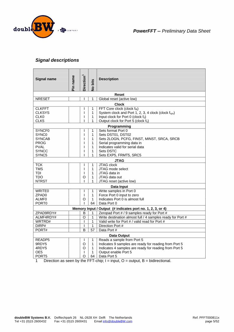
Signal descriptions
Signal name
Pin
nam
e
Dir
ecti
on
1
No
bit
s Description
ResetNRESET I 1 Global reset (active low)
ClockCLKFFT I 1 FFT Core clock (clock ffft)CLKSYS I 1 System clock and Port 1, 2, 3, 4 clock (clock fsys)CLK0 I 1 Input clock for Port 0 (clock f0)CLK5 I 1 Output clock for Port 5 (clock f5)
ProgrammingSYNCF0 I 1 Sets format Port 0SYNC0 I 1 Sets DST01, DST02SYNCAB I 1 Sets 2LOGN, PCFG, FINST, MINST, SRCA, SRCBPROG I 1 Serial programming data inPVAL I 1 Indicates valid for serial dataSYNCC I 1 Sets DSTCSYNC5 I 1 Sets EXP5, FRMT5, SRC5
JTAGTCK I 1 JTAG clockTMS I 1 JTAG mode selectTDI I 1 JTAG data inTDO O 1 JTAG data outNTRST I 1 JTAG reset (active low)
Data InputWRITE0 I 1 Write samples in Port 0ZPAD0 I 1 Force Port 0 input to zeroALMF0 O 1 Indicates Port 0 is almost fullPORT0 I 64 Data Port 0
Memory Input / Output (# indicates port no. 1, 2, 3, or 4)ZPAD9RDY# B 1 Zeropad Port # / 9 samples ready for Port #ALMF4RDY# O 1 Write destination almost full / 4 samples ready for Port #WRTRD# I 1 Valid write for Port # / valid read for Port #DIRP# I 1 Direction Port #PORT# B 57 Data Port #
Data OutputREADP5 I 1 Reads a sample from Port 59RDY5 O 1 Indicates 9 samples are ready for reading from Port 54RDY5 O 1 Indicates 4 samples are ready for reading from Port 5OE5 I 1 Output enable Port 5PORT5 O 64 Data Port 51 Direction as seen by the FFT-chip; I = input, O = output, B = bidirectional.

PowerFFT -- Preliminary Data Sheet
doubleBW Systems B.V. Delftechpark 26 NL-2628 XH Delft The Netherlands Ref. PFFT000811xTel +31 (0)15 2600432 Fax +31 (0)15 2600431 Email [email protected] page 6/52
Clock domains
Clock domain
Pin
nam
e
Signal name Description
Asynch NRESETNTRST
Asynch
CLKFFT - FFT domainCLKSYS SYNC0
SYNCABSYNCCSYNC5PROGPVALPORT#(56:0)DIR#WRTRD#ZPAD9RDY#ALMF4RDY#
System domain
CLK0 SYNCF0PORT0(63:0)WRITE0ZPAD0ALLMF0
Input domain
CLKP5 PORT5(63:0)READ54RDY59RDY5OE5
Output domain
TCK TMSTDITDO
JTAG domain(~1 MHz)
Power supply pins
Type Pin namesGround (GND)Supply voltage (VDD)
Pin layout
TBD

PowerFFT -- Preliminary Data Sheet
doubleBW Systems B.V. Delftechpark 26 NL-2628 XH Delft The Netherlands Ref. PFFT000811xTel +31 (0)15 2600432 Fax +31 (0)15 2600431 Email [email protected] page 7/52
Functional description
Functional block diagram
Processing Core
Crossbar Switch
Port AConverter
Port BConverter
Port CConverter
FIFO FIFO FIFO
Po
rt 0
Co
nve
rter
FIF
O
Po
rt 5
Co
nve
rter
FIF
O
FIFO FIFO FIFO FIFO
Shift Register
Port 0
prog
CLK0 CLK5
CLKFFT
CLKSYSTCK
JTAGJTAG
Port 5
Port 1 Port 2 Port 3 Port 4
The data path is developed for stream-wise processing of data. In principle, the user feedsthe PowerFFT with data sequences at the primary input port PORT0. Handshakemechanisms prevent the user from "overfeeding" PORT0 (almost full flag). Valid data isindicated by the user through a valid signal. After a processing latency, the result datasequences are written on the primary output port PORT5. Data ready flags indicates that theuser can read data samples.
Processing CoreThe Processing Core consists of a Multiply Core and an FFT core, connected to memory witha Switch. The Switch is set through a configuration control word PCFG.
MultiplyCore
A
BSwitch
FFTCore
XFFT
PCFG = "10"
PCFG = ”01"PCFG = "00"
PCFG = "11"
FFT
FFT
A
B
A
B
A
B B
4 configurations
PCFG
X
XX
C
C
C C
C
Through the Switch settings, the Processing Core can operate in 4 configurations:

PowerFFT -- Preliminary Data Sheet
doubleBW Systems B.V. Delftechpark 26 NL-2628 XH Delft The Netherlands Ref. PFFT000811xTel +31 (0)15 2600432 Fax +31 (0)15 2600431 Email [email protected] page 8/52
• Multiply Core preceding the FFT Core;• Multiply Core behind the FFT Core;• Stand alone Multiply Core (FFT Core disabled);• Multiply Core behind the FFT Core, single input.
Generally, the Multiply Core is used for vector multiplication in combination with an FFT Coreoperation. A clear example is windowing a sequence before it is FFTed. Processing Core isrunning on the system clock CLKSYS, but the FFT Core is running on a separate FFT clockCLKFFT.
Multiply Core descriptionThe Multiply Core executes multiplication in a stream-wise manner. The Multiply Core canoperate on two input samples A and B in the following 4 modes:
• MultiplyA × B
• Conjugate multiplyA × conj(B)
• Transparantignore A, pass B
• Conjugateignore A, pass conj(B)
The Multiply Core operates on a sequence to sequence basis, i.e. the modes can be changedfrom sequence to sequence.
FFT Core descriptionThe FFT Core executes FFT-operations on subsequent sequences in a stream-wise manner.The FFT Core can operate in four basic modes:
• FFT(I)FFT (with or without spectrum shift)
• Fast convolutionFFT on first sequence, FFT on second, (conjugate) multiply results, and IFFT
• Spectrum multiplicationFFT first sequence, (conjugate) multiply with second sequence, and IFFT
• Multiply and FFT(conjugate) multiply first sequence with second sequence, (I)FFT the result
Note that the internal multipliers in the FFT Core (i.e., the coefficient multiplier in the Radix-2units) are used for multiplication. In this way, four parallel multipliers can operate on thesystem clock. The spectrum shift is optional for the FFT function: the result can be either aspectrum from 0 to 2π, or from -π to π. The FFT Core operates on 16, 32, 64, 128, and 256length sequences in batch mode, that is, the same instruction is executed on 512/Nsubsequent sequence, with N the sequence length. For sequences of length 512 or 1024, theinstruction may alternate from sequence to sequence.

PowerFFT -- Preliminary Data Sheet
doubleBW Systems B.V. Delftechpark 26 NL-2628 XH Delft The Netherlands Ref. PFFT000811xTel +31 (0)15 2600432 Fax +31 (0)15 2600431 Email [email protected] page 9/52
4 x parallelRadix-2
Outputbuffer
CLKFFT domain
5757
Inputbuffer 456 Switch
4 x coeff .
8 x data
456 456
456
Coeff .ROM
228
Notes on execution times for the FFT CoreThe FFT Core consists of 4 parallel radix-2, effectively executing 4 butterfly operations (i.e,radix-2 operations) in one clock cycle (system clock frequency fsys). The no. of butterflies in anN-point FFT is N/2 log(N), thus an N-point FFT is executed in N/8 log(N) clock cycles. Theeffective execution time of an N-point FFT is thus Tfft = N/8 log(N)/ffft seconds. Note that theI/O time of an N-length sequence is determined by the system clock TIO = N/fsys. From anutilization point of view, an optimum balance between IO and processing execution time isachieved if Tfft = TIO, hence ffft/fsys = log(N)/8. In worst case, for maximum N = 1024, thismeans ffft/fIO = 1.28. In case the FFT Core executes the multiply operation on N-points, itutilizes all four internal multipliers of the radix-2 in parallel. Thus the effective execution timeof a multiply is Tmul = (40 + N/4)/4f fft. (The 40 additional cycles are introduced by an additionalpipeline delay).
Instruction Execution time ( x 1/ffft sec)FFT N/8 log(N)FFT1 / FFT2 / MPY / IFFT 3N/8 log(N) + N/4 + 40FFT1 / MPY2 / IFFT 2N/8 log(N) + N/4 + 40MPY / FFT N/8 log(N) + N/4 + 40
Processing Core settingsThe Processing Core is set using the 16 bits instruction SET_PROCESSING_CORE,consisting of the following 4 control words (see also the section on control words):
PCFG Configuration of the Processing CoreMINST Instruction for the Multiply CoreFINST Instruction for the FFT Core2LOGN Two-log of the length of FFT sequences
In the following table, the relevant instructions SET_PROCESSING_CORE are listed. Thearrows determine the order of Multiply Core and FFT Core operations. In the table only batchand non-batch modes are distinguished. For a detailed listing of the 24 FFT instructionsFINST is referred to the section on the control words.

PowerFFT -- Preliminary Data Sheet
doubleBW Systems B.V. Delftechpark 26 NL-2628 XH Delft The Netherlands Ref. PFFT000811xTel +31 (0)15 2600432 Fax +31 (0)15 2600431 Email [email protected] page 10/52
Control wordsSET_PROCESSING_CORE description PCFG MINST FINST1 2LOGN2
Multiply → FFT "00" "00" 00 … 11 9, 10Conj. Multiply → FFT "00" "01" 00 … 11 9, 10Conjugate → FFT "00" "11" 00 … 11 9, 10Transparent → FFT (stand-alone FFT) "00" "10" 00 … 11 9, 10FFT → Multiply "01" "00" 00 … 11 9, 10FFT → Conj. Multiply "01" "01" 00 … 11 9, 10FFT → Detection "11" "01" 00 … 11 9, 10FFT → Conjugate "01" "11" 00 … 11 9, 10FFT → Transparent (stand-alone FFT) "01" "10" 00 … 11 9, 10Multiply → Batch FFT "00" "00" 12 … 23 4 … 8Conj. Multiply → Batch FFT "00" "01" 12 … 23 4 … 8Conjugate → Batch FFT "00" "11" 12 … 23 4 … 8Transparent → Batch FFT (stand-alone FFT) "00" "10" 12 … 23 4 … 8Batch FFT → Multiply "01" "00" 12 … 23 4 … 8Batch FFT → Conj. Multiply "01" "01" 12 … 23 4 … 8Batch FFT → Detection "11" "01" 12 … 23 4 … 8Batch FFT → Conjugate "01" "11" 12 … 23 4 … 8Batch FFT → Transparent (stand-alone FFT) "01" "10" 12 … 23 9, 10Stand-alone Multiply "10" "00" Don't care Don't careStand-alone Conj. Multiply "10" "01" Don't care Don't care1 Reference to the instructions listed in the table on FINST in section on control words.2 Actual value, see section on control words for formatting.
Crossbar Switch settingsThe Crossbar Switch connects input Port 0, memory Ports 1 to 4, output Port 5 and theinternal Processing Core Ports A, B and C. The Crossbar Switch can set three independentseparated data path settings, set by the Control Words. The following classes of data pathsettings are distinguished:
Input: from Port 0 straight to one or two memory portsThroughput: all paths through the Processing CoreOutput: from one memory port to Port 5
The schematic view of the Crossbar Switch is as follows:
Crossbar Switch0 5
# $ @ &
A B C
Note that the memory ports are referred to as #, $, @, and &, rather than 1…4, indicating theindividual ports, without assigning a specific number to each port. The Crossbar Switch is nowset using the 18 bits instruction SET_CROSSBAR_SWITCH, consisting of the followingcontrol words:
DST01 First destination of Port 0

PowerFFT -- Preliminary Data Sheet
doubleBW Systems B.V. Delftechpark 26 NL-2628 XH Delft The Netherlands Ref. PFFT000811xTel +31 (0)15 2600432 Fax +31 (0)15 2600431 Email [email protected] page 11/52
DST02 Second destination of Port 0 (data put on Port 0 can be written simultaneouslyinto two memory ports)
SRCA Source of Port ASRCB Source of Port BDSTC Destination of Port CSRC5 Source of Port 5
NOTE: If the destination of Port 0 is either Port A or Port B, no distinction is made betweenthe Port A and Port B destination of Port 0 (indicated by the destination "AB"). Thisdistinction is uniquely set by assigning the proper source for Ports A and B.
In the following table, the relevant SET_CROSSBAR_SWITCH instructions are listed withregards to the throughput path. The possible SET_CROSSBAR_SWITCH settings aredesignated using the following conventions:
CSTxx() Crossbar Switch Throughput setting no. xx. In total, 19 throughput settings areavailable, indicated by xx = 00 to 18. If applicable, memory ports are includedbetween the brackets as variables. These settings uniquely designate eachpossible data path through the Processing Core.
CSIx() Crossbar Switch Input setting no. x. In total, 3 input settings are available,indicated by x = 0 to 2. If applicable, memory ports are included between thebrackets as variables. These settings uniquely designate each possible data pathfrom Port 0 straight to one of the memory ports.
CSOx() Crossbar Switch Output setting no. x. In total, 2 output settings are available,indicated by x = 0 to 1. If applicable, memory ports are included between thebrackets as variables. These settings uniquely designate each possible data pathfrom one of the memory ports straight to Port 5.
The "-" setting indicates that the port is set to "not used". Note that the Crossbar Switchparameters correspond to control words, described in the control word section. Thethroughput, input and output settings uniquely set the proper bits in theSET_CROSSBAR_SWITCH instruction, or more specific, in its control words DST01, DST02,SRCA, SRCB, DSTO, and SRC5. For example:
• CST02(#) sets DST01, DST02, SRCA, SRCB, DSTO, and SRC5;• CST08(#,$) sets DST01, DST02, SRCA, SRCB, and DSTO, and should thus be
accompanied by, e.g., CSO1(@) that sets SRC5;• CST13(#,$,@) sets SRCA, SRCB, and DSTO, and should thus be accompanied by, e.g.,
CSI0() that sets DST01 and DST02, and CSO1(&) that sets SRC5;• CST16(#,$) sets SRCA, SRCB, DSTO, and SRC5, and should thus be accompanied by,
e.g., CSI2(@,&) that sets DST01 and DST02.
NOTE 1: Not all throughput, input and output setting combinations are allowed. For example,CST13(#,$,@) occupies 3 memory ports for the throughput path setting,CSI2(#,$)occupies 2 memory ports for the input path setting, and CSO1(&), involve1 memory port for the output path setting, whereas only 4 memory ports in total canbe occupied. That is why the combination CST13(#,$,@), CSI0(), and CSO1(&) isallowed, as this combination only occupies 4 memory ports.
NOTE 2: To force that all control words DST01, DST02, SRCA, SRCB, DSTO, and SRC5 areset, unlike that some are unused, so-called NULL control strings are defined:CST04(), CSTT13(), CST14(), CSI0(), and CSO0(). They should be used to set theunused control words to "not used".

PowerFFT -- Preliminary Data Sheet
doubleBW Systems B.V. Delftechpark 26 NL-2628 XH Delft The Netherlands Ref. PFFT000811xTel +31 (0)15 2600432 Fax +31 (0)15 2600431 Email [email protected] page 12/52
Control wordsSET_CROSSBAR_SWITCHthroughput settings DST01 DST02 SRCA SRCB DSTC SRC5
CST00() AB AB - 0 5 CCST01(#) AB AB 0 # 5 CCST02(#) AB AB # 0 5 CCST03() AB AB 0 0 5 CCST04() - - - - -CST05(#) AB AB - 0 #CST06(#) AB AB 0 0 #CST07(#) AB AB - 0 #CST08(#,$) AB AB 0 # $CST09(#,$) AB AB # 0 $CST10() - - -CST11(#,$) - # $CST12(#,$) # # $CST13(#,$,@) # $ @
OUTPUTSETTINGS
CST14() - - - -CST15(#) - # 5 CCST16(#,$) # $ 5 CCST17(#)
INPUTSETTINGS
# # 5 C
Control wordsSET_CROSSBAR_SWITCHinput settings DST01 DST02 SRCA SRCB DSTC SRC5
CSI0() - -CSI1(#) # #CSI2(#,$) # $
THROUGHPUT / OUTPUT SETTINGS
Control wordsSET_CROSSBAR_SWITCHoutput settings DST01 DST02 SRCA SRCB DSTC SRC5
CSO0() -CSO1(#) INPUT / THROUGHPUT SETTINGS #
Data formats settings
Hybrid long formatThe internal data format of the Processing Core arithmetic is a 57 bits hybrid floating pointformat ("hybrid long"). The hybrid long format is selected to preserve IEEE floating pointaccuracy, but with more effective utilization of available silicon (see the subsection onaccuracy). The hybrid long format consist of a 24 bits real mantissa RE, a 24 bits imaginarymantissa IM and a 9 bits common exponent EXP, all represented in two's complementintegers. Note that each number has a unique EXP, unlike the block floating point format,where an exponent is shared by the mantissas of a vector. A hybrid long complex number isrepresented as:
EXP RE IMBit no. 56…48 47…24 23…0
Real part = RE × 2EXP Imaginary part = IM × 2EXP

PowerFFT -- Preliminary Data Sheet
doubleBW Systems B.V. Delftechpark 26 NL-2628 XH Delft The Netherlands Ref. PFFT000811xTel +31 (0)15 2600432 Fax +31 (0)15 2600431 Email [email protected] page 13/52
Hybrid short formatA special format introduced is the 32 bits hybrid floating point format ("hybrid short"). Thisformat is only used when only 32 bits data ports are available, for example due external buslimitations. The hybrid short format consist of a 12 bits real mantissa RE, a 12 bits imaginarymantissa IM and a 8 bits common exponent EXP, all represented in two's complementintegers. A hybrid short complex number is represented as:
EXP RE IMBit no. 31…24 23…12 11…0
Real part = RE × 2EXP Imaginary part = IM × 2EXP
Port 0 and Port 5 data formatsThe following data formats are available for the Port 0 and Port 5 ports (see also thesubsections on the FRMT0 and the FRMT5 control words):
Format Descriptionhybrid long See abovehybrid short See aboveshort integer* 16 bits two's complement fixed pointinverted sign short* Short integer, sign bit (bit no. 15) invertedlong integer* 32 bits two's complement fixed pointinverted sign long* Long integer, sign bit (bit no. 31) invertedfloating point* IEEE floating point
The formats marked * can be offered sequential or parallel. In sequential mode two clockcycles are required to write a complex number: the real part on the 1st cycle, the imaginarypart on the 2nd cycle. In parallel mode a complete number is written in a single clock cycle.The occupation of the bit nos. for the 64 bits on Port 0 or Port 5 is as follows:
Bit nos.Format Mode
Real Imaginaryhybrid long N.A. 56…0hybrid short N.A. 31…0short integer sequential 15…0
parallel 31…16 15…0inverted sign short sequential 15…0
parallel 31…16 15…0long integer sequential 31…0
parallel 63…32 31…0inverted sign long sequential 31…0
parallel 63…32 31…0floating point sequential 31…0
parallel 63…32 31…0
In the integer and sign inverted integer formats it is required to apply a block exponentDES_EXP in the conversion from the hybrid long format into one of the fixed point formats(see the control word EXP5). The actual values can be derived from the integer values REand IM as follows (RE and IM refer to the real and imaginary integer numbers as provided bythe Ports):
Actual real part = RE × 2DES_EXP Actual imaginary part = IM × 2DES_EXP
PowerFFT -- Preliminary Data Sheet
doubleBW Systems B.V. Delftechpark 26 NL-2628 XH Delft The Netherlands Ref. PFFT000811xTel +31 (0)15 2600432 Fax +31 (0)15 2600431 Email [email protected] page 14/52
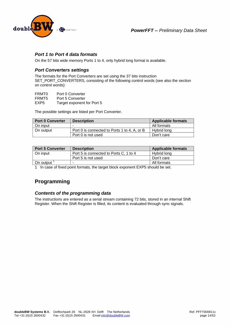
Port 1 to Port 4 data formatsOn the 57 bits wide memory Ports 1 to 4, only hybrid long format is available.
Port Converters settingsThe formats for the Port Converters are set using the 37 bits instructionSET_PORT_CONVERTERS, consisting of the following control words (see also the sectionon control words):
FRMT0 Port 0 ConverterFRMT5 Port 5 ConverterEXP5 Target exponent for Port 5
The possible settings are listed per Port Converter.
Port 0 Converter Description Applicable formatsOn input - All formats
Port 0 is connected to Ports 1 to 4, A, or B Hybrid longOn outputPort 0 is not used Don’t care
Port 5 Converter Description Applicable formatsPort 5 is connected to Ports C, 1 to 4 Hybrid longOn inputPort 5 is not used Don’t care
On output 1 - All formats1 In case of fixed point formats, the target block exponent EXP5 should be set.
Programming
Contents of the programming dataThe instructions are entered as a serial stream containing 72 bits, stored in an internal ShiftRegister. When the Shift Register is filled, its content is evaluated through sync signals.

PowerFFT -- Preliminary Data Sheet
doubleBW Systems B.V. Delftechpark 26 NL-2628 XH Delft The Netherlands Ref. PFFT000811xTel +31 (0)15 2600432 Fax +31 (0)15 2600431 Email [email protected] page 15/52
Instructions / control words Bit no. DescriptionSRESET 71 Synchronous resetSET_PROCESSING_CORE 70 down to 55
PCFG 70 down to 69 Configuration of the Processing Corereserved 68 down to 67 "00"MINST 66 down to 65 Instruction for the Multiply CoreFINST 64 down to 59 Instruction for the FFT Core2LOGN 58 down to 55 Two-log of the length of FFT sequences
SET_CROSSBAR_SWITCH 54 down to 37DST01 54 down to 52 First destination of Port 0DST02 51 down to 49 Second destination of Port 0SRCA 48 down to 46 Source of Port ASRCB 45 down to 43 Source of Port BDSTC 42 down to 40 Destination of Port CSRC5 39 down to 37 Source of Port 5
SET_PORT_CONVERTORS 54 down to 37FRMT0 36 down to 32 Port 0 Converter formatReserved 31 down to 29 "000"Reserved 28 down to 26 "000"Reserved 25 down to 23 "000"Reserved 22 down to 14 "000000000"FRMT5 13 down to 9 Port 5 Converter formatEXP5 8 down to 0 Target exponent for Port 5
Filling the Shift RegisterThe programming data PROG is stored in the Shift Register in 72 clock cycles CLKSYS. Thestart and termination of the valid data is determined through the PVAL signal.
Bit 0 Bit 1 Bit 2 Bit 71PROG
PVAL
CLKSYS
CONTROL WORD (N-1:0)
SYNC
CLOCK
Old control word New control word
Transfer of the control words from the Shift Register to the logicFive sync signals determine when the control words in the programming data, after they arestored in the Shift Register, are transferred to the logic. The sync signals are offeredindependently. Upon a sync, all relevant control words are evaluated in parallel (i.e.,transferred to the logic).

PowerFFT -- Preliminary Data Sheet
doubleBW Systems B.V. Delftechpark 26 NL-2628 XH Delft The Netherlands Ref. PFFT000811xTel +31 (0)15 2600432 Fax +31 (0)15 2600431 Email [email protected] page 16/52
Sync Control word Clock domainSYNCF0 FRMT0 CLK0
DST01SYNC0
DST02SRESETPCFGMINSTFINST2LOGNSRCA
SYNCAB
SRCBSYNCC DSTC
SRC5FRMT5SYNC5EXP5
CLKSYS
The user is referred to the Data Flow Chart for syncing rules. The syncing rules aredetermined either for an input, a throughput or an output sequence (or in other words, to theCrossbar Switch settings). Basically, the user who wants to set the control words uponoffering (a) data sequence(s), should verify the syncing rules for the desired setting. Note thatsome cases may involve input, output and throughput settings simultaneously. For eachsetting the syncing rules should be verified.
NOTE: The syncing rules described below do not hold for SYNCF0. The rule for SYNCF0 issimple: upon a SYNCF0, the control word FRMT0 is active on the next input sampleon Port 0.
Data Flow Chart decisions1 After reset no specific sync rules applies.2 Different (and more complex) syncing rules apply for throughput settings than for input
and output settings.3 The data path of the desired throughput setting may conflict with a current input or output
setting. For example, throughput setting CST00() is desired and input setting CSI1(#) isstill active, then a conflict occurs for control words DST01 and DST02. In that casesetting CST00() is only allowed after CSI1(#) is not active anymore, which is if the lastsample of the current sequence is read from the chip.
4 If the Processing Core configuration involves the FFT Core, then upon syncing thedesired throughput settings are delayed until the current sequences within theProcessing Core are processed. If the Processing Core configuration is in multiply onlymode, upon syncing the desired settings are invoked immediately. To make sure that thecurrent sequence is finished in multiply only mode, the user should sync the settings inthis case after the last multiply only result is read from the chip.
5 The Processor Configuration (PCFG control word) cannot be changed on the fly. Forexample, if the desired configuration is a multiply à FFT, and the current configuration isan multiply à FFT only, the syncing should be done after the last result sample is readfrom the chip.
6 A memory port cannot be assigned as source if it is scheduled as a destination for thecurrent setting or previous settings that are still to be finalized. (Basically, this ruleprevents from reading data from a memory, before it is written into the memory.)
7 Desired settings synced after 128th samples of the current sequence are written into thechip, are automatically assigned to the next sequence.
8 In case the FFT instruction FINST is a two-phase function, a two-phase sync ruleapplies. For each phase different Crossbar Switch settings may apply, but Processing

PowerFFT -- Preliminary Data Sheet
doubleBW Systems B.V. Delftechpark 26 NL-2628 XH Delft The Netherlands Ref. PFFT000811xTel +31 (0)15 2600432 Fax +31 (0)15 2600431 Email [email protected] page 17/52
Core configuration and Data Format settings must be the same. The desired settings forthe 1st phase of the instruction are synced between the 128th sample and the last sampleof the current sequence, and the desired settings for the 2nd phase of the instruction arebetween the 128th sample and the last sample of the 1st phase sequence (seeexplanation of Data Flow Chart actions).
9 See item 8.10 The data path of the desired input or output setting may conflict with a current input or
output setting. For example, input setting CSI2(1,3) is desired and output settingCSO1(3) is still active, then a conflict occur for control words DST02 and SRC5. In thatcase setting CSI2(1,3) is only allowed after CSO1(3) is not active anymore, which is ifthe last sample of the current sequence is read from the chip.
11 If the Processing Core configuration involves the FFT Core, upon syncing the desiredinput or output settings are delayed until the current sequences within the ProcessingCore are processed. If the Processing Core configuration is in multiply only mode, uponsyncing the desired settings invoked immediately. To make sure that the currentsequence is finished in multiply only mode, the user should sync the settings in this caseafter the last multiply only result is read from the chip.
12 A memory port cannot be assigned as source or destination if it is scheduled for thecurrent setting or previous settings that are still to be finalized.
Data Flow Chart processes1 Some desired throughput settings are active immediately upon syncing. To be sure that
the desired settings do not affect the current operation, syncing is only allowed if all datasamples currently involved are read from the chip.
2 Two-phased instructions involve two operations by the Processing Core on sequences.For example, 1st phase: FFT; 2nd phase: multiply à IFFT. This means that twosubsequent syncing actions are required with different syncing rules. (See tables below).
3 1st phase settings are synced at 128th sample of current sequence, and the 2nd phasesettings are synced at 128th sample of the 1st phase sequence.
4 See item 2 and 3.5 Desired input and output settings are active immediately upon syncing. To be sure that
the desired input and output settings do not affect the current operation, syncing is onlyallowed if all data samples currently involved have been read from the chip.
6 Desired input and output settings are synced upon offering the first sample of thecorresponding sequence.

PowerFFT -- Preliminary Data Sheet
doubleBW Systems B.V. Delftechpark 26 NL-2628 XH Delft The Netherlands Ref. PFFT000811xTel +31 (0)15 2600432 Fax +31 (0)15 2600431 Email [email protected] page 18/52
1st phase throughput syncs1st phase throughputsettings SYNCF0 SYNC0 SYNCAB SYNCC SYNC5
CST00() X X X XCST01(#) X X X XCST02(#) X X X XCST03() X X X XCST04() X X XCST05(#) X X XCST06(#) X X XCST07(#) X X XCST08(#,$) X X XCST09(#,$) X X XCST10() X XCST11(#,$) X XCST12(#,$) X XCST13(#,$,@) X X
NOTAPPLI-CABLE
CST14() X X XCST15(#) X X XCST16(#,$) X X XCST17(#)
NOT APPLICABLE
X X X
2nd phase throughput syncs2nd phase throughputsettings SYNCF0 SYNC0 SYNCAB SYNCC SYNC5
CST00() X XCST01(#) X XCST02(#) X XCST03() X XCST04() X XCST05(#) X XCST06(#) X XCST07(#) X XCST08(#,$) X XCST09(#,$) X XCST10() XCST11(#,$) XCST12(#,$) XCST13(#,$,@) X
NOTAPPLI-CABLE
CST14() XCST15(#) XCST16(#,$) XCST17(#)
NOT APPLICABLE
X
Input syncsInput settingsSYNCF0 SYNC0 SYNCAB SYNCC SYNC5
CSI0() xCSI1(#) XCSI2(#,$) X
NOT APPLICABLE

PowerFFT -- Preliminary Data Sheet
doubleBW Systems B.V. Delftechpark 26 NL-2628 XH Delft The Netherlands Ref. PFFT000811xTel +31 (0)15 2600432 Fax +31 (0)15 2600431 Email [email protected] page 19/52
Output syncsOutput settingsSYNCF0 SYNC0 SYNCAB SYNCC SYNC5
CSO0() XCSO1(#) NOT APPLICABLE X
is desired Crossbar Switchsetting a throughput setting?
conflict desiredCrossbar Switch setting with current
input or output setting?
involves current setting PCFGin multiply only mode?
is setting first after reset?
is desired source memory portscheduled as destination port?
wait until lastsample of current
throughput sequenceis read from chip
implies desired setting PCFG change?
wait
sync 1st phasesettings
is 128th sample from current input sequence written to chip?
wait
involves desired setting a repeat(two-phase) instruction?
Y
Y
Y
Y
Y
N
N
N
Y
N
N
N
Y
N
N
Y
1
2
3
4
5
6
7
8
wait for nextsequence
sync 2nd phasesettings
is 128th sample from current input sequence written to chip?
waitN
Y
9
is desired source or destinationmemory port scheduled?
wait until lastsample of current input
/ output sequence isread from chip
conflict desiredCrossbar Switch setting with current
input or output setting?
wait
syncsettings
Y
N
N
10
12
Yconflict with current throughput setting PCFG in multiply only mode?
N
11
Y
1
2
3
4
5
6

PowerFFT -- Preliminary Data Sheet
doubleBW Systems B.V. Delftechpark 26 NL-2628 XH Delft The Netherlands Ref. PFFT000811xTel +31 (0)15 2600432 Fax +31 (0)15 2600431 Email [email protected] page 20/52
InstructionsThe 72 bits programming data consists of three instructions and a synchronous reset bit:
SR
ES
ET
SET_PROCESSING_CORE(16 bits)
SET_CROSSBAR_SWITCH(18 bits)
SET_PORT_CONVERTERS(37 bits)
71 70 55 54 37 36 0
SRESETThe SRESET is used to clear all current active Control Words. It acts as a synchronous resetof the chip.
Format Description0 Reset1 no reset
SET_PROCESSING_CORE
PCFG "00" MINST FINST 2LOGN
15 14 13 12 11 10 9 4 3 0
PCFGThe CFG specifies the 4 different configurations of the Processing Core (see also subsectionon Processing Core).
Format Description00 Multiply Core preceding the FFT Core01 Multiply Core behind the FFT Core10 Stand alone Multiply Core (FFT Core disabled)11 Multiply Core behind the FFT Core, single input
MINSTMultiply Core instruction MINST set the Multiply Core in 4(3) modes (see also subsection onMultiply Core):
Format Description00 Multiply: A x B01 Conjugate multiply: A x conj(B)10 Transparent: pass B11 Conjugate: pass conj(B)
FINSTThe FINST specifies the modes of the FFT Core in the Processing Core. There are four basicFFT Core instructions, indicated by the first two bits 0 and 1 (see also subsection on FFTCore). The remaining four bits specify the FFT direction (inverse), conjugate multiply, batchmode, and shift mode of the FFT.

PowerFFT -- Preliminary Data Sheet
doubleBW Systems B.V. Delftechpark 26 NL-2628 XH Delft The Netherlands Ref. PFFT000811xTel +31 (0)15 2600432 Fax +31 (0)15 2600431 Email [email protected] page 21/52
← S
hift
flag
← B
atch
flag
← C
onju
gate
flag
← In
vers
e F
FT
flag
← F
FT
Cor
e m
odes
FINST 5 4 3 2 1 0
Format InstructionXXXX00 FFTXXXX01 FFT1 / FFT2 / MPY / IFFTXXXX10 FFT1 / MPY2 / IFFTXXXX11 MPY / FFT
NOTE 1: The multiply function is executed by the internal multiplier within the radix 2processors, and not by the Multiply Core. The Multiply Core can be combined withany of the FFT modes specified by the FINST through the PCFG control word.
NOTE 2: For sequences of 256 points or less a batch mode is developed to prevent pausesbetween sequences. In batch mode multiple sequences are entered until 512 pointsare reached. On each sequence within the batch the same instruction is executed.
NOTE 3: The FINST distinguishes "one-phase" instructions (operating on a single sequence)or "two-phase" instructions (operating on two subsequent sequences). In the latercase, the same instruction must be applied on the second sequence (or batch ofsequences).

PowerFFT -- Preliminary Data Sheet
doubleBW Systems B.V. Delftechpark 26 NL-2628 XH Delft The Netherlands Ref. PFFT000811xTel +31 (0)15 2600432 Fax +31 (0)15 2600431 Email [email protected] page 22/52
FIN
ST
lab
el Format
Sh
ift
mo
de
Bat
ch m
od
e
Co
nj.
mu
ltip
ly
Inve
rse
FF
T
2LO
GN
val
ue
Tw
o-p
has
ed
Description
00 000000 9,10 FFT01 000100 X 9,10 IFFT02 000001 9,10 X FFT1 / FFT2 / MPY / IFFT03 000010 9,10 X FFT1 / MPY2 / IFFT04 000011 9,10 X MPY / FFT05 000111 X 9,10 X MPY / IFFT06 001001 X 9,10 X FFT1 / FFT2 / CONJ. MPY / IFFT07 001010 X 9,10 X FFT1 / CONJ. MPY2 / IFFT08 001011 X 9,10 X CONJ. MPY / FFT09 001111 X X 9,10 X CONJ. MPY / IFFT10 100000 X 9,10 SHIFT FFT11 100100 X X 9,10 SHIFT IFFT12 010000 X 4…8 BATCH FFT13 010100 X X 4…8 BATCH IFFT14 010001 X 4…8 X BATCH FFT1 / FFT2 / MPY / IFFT15 010010 X 4…8 X BATCH FFT1 / MPY2 / IFFT16 010011 X 4…8 X BATCH MPY / FFT17 010111 X X 4…8 X BATCH MPY / IFFT18 011001 X X 4…8 X BATCH FFT1 / FFT2 / CONJ. MPY / IFFT19 011010 X X 4…8 X BATCH FFT1 / CONJ. MPY2 / IFFT20 011011 X X 4…8 X BATCH CONJ. MPY / FFT21 011111 X X X 4…8 X BATCH CONJ. MPY / IFFT22 110000 X X 4…8 SHIFT BATCH FFT23 110100 X X X 4…8 SHIFT BATCH IFFT
2LOGNThe 2LOGN is the base 2 logarithm of the number of data points for the Processing Core.
NOTE: For 2LOGN from 4 to 8 (i.e. from 16 to 256 points) are packed in batches of 512points. The Processing Core executes the same operation on all sequences in onebatch (see also control word FINST).
Format Description4 bits unsigned integer Base 2 logarithm,
range 0100 (4) … 1010 (10)
SET_CROSSBAR_SWITCH
DST01 DST02 SRCA SRCB DSTC SRC5
17 15 14 12 11 9 8 6 5 3 2 0

PowerFFT -- Preliminary Data Sheet
doubleBW Systems B.V. Delftechpark 26 NL-2628 XH Delft The Netherlands Ref. PFFT000811xTel +31 (0)15 2600432 Fax +31 (0)15 2600431 Email [email protected] page 23/52
DST01The DST01 determines the first setting of the Crossbar Switch with respect to the Port 0, i.e.,the first destination of the data from Port 0. See the section on the Crossbar Switch fordetails.
Format Description001 Destination Port 1010 Destination Port 2011 Destination Port 3100 Destination Port 4110 Destination Processing Core (Port A or B)111 Port 0 data not used
DST02The DST02 determines the second setting of the Crossbar Switch with respect to the Port 0,i.e., the second destinations of the data from Port 0. If DST02 is the same as DST01, the Port0 data has only one destination. See the section on the Crossbar Switch for details.
Format Description001 Destination Port 1010 Destination Port 2011 Destination Port 3100 Destination Port 4110 Destination Processing Core (Port A or B)111 Port 0 data not used
SRCAThe SRCA determines the setting of the Crossbar Switch with respect to Port A converter,i.e., the source of the data transferred to the Port A converter. See the section on theCrossbar Switch for details.
Format Description000 Data taken from Port 0 (source Port 0)001 Data taken from Port 1 (source Port 1)010 Data taken from Port 2 (source Port 2)011 Data taken from Port 3 (source Port 3)100 Data taken from Port 4 (source Port 4)111 Port A is not used
SRCBThe SRCB determines the setting of the Crossbar Switch with respect to Port B converter, i.e.the source of the data transferred to the Port B converter. See the section on the CrossbarSwitch for details.
Format Description000 Data taken from Port 0 (source Port 0)001 Data taken from Port 1 (source Port 1)010 Data taken from Port 2 (source Port 2)011 Data taken from Port 3 (source Port 3)100 Data taken from Port 4 (source Port 4)111 Port B is not used
PowerFFT -- Preliminary Data Sheet
doubleBW Systems B.V. Delftechpark 26 NL-2628 XH Delft The Netherlands Ref. PFFT000811xTel +31 (0)15 2600432 Fax +31 (0)15 2600431 Email [email protected] page 24/52
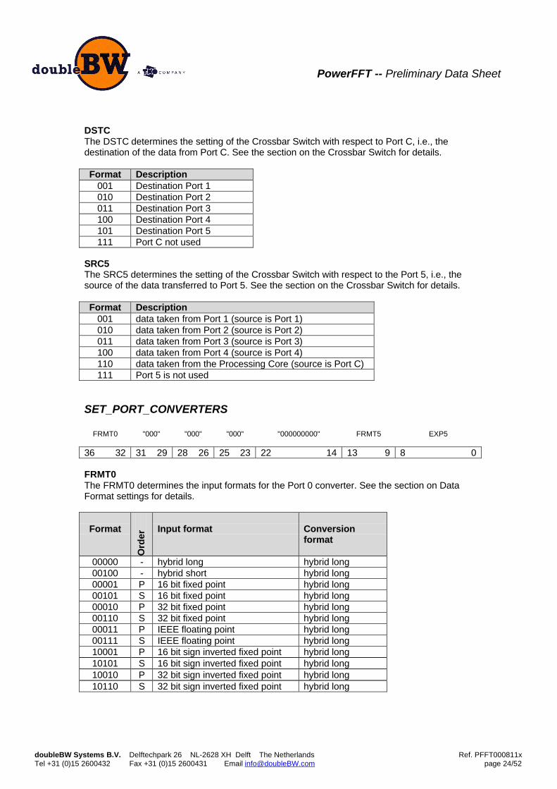
DSTCThe DSTC determines the setting of the Crossbar Switch with respect to Port C, i.e., thedestination of the data from Port C. See the section on the Crossbar Switch for details.
Format Description001 Destination Port 1010 Destination Port 2011 Destination Port 3100 Destination Port 4101 Destination Port 5111 Port C not used
SRC5The SRC5 determines the setting of the Crossbar Switch with respect to the Port 5, i.e., thesource of the data transferred to Port 5. See the section on the Crossbar Switch for details.
Format Description001 data taken from Port 1 (source is Port 1)010 data taken from Port 2 (source is Port 2)011 data taken from Port 3 (source is Port 3)100 data taken from Port 4 (source is Port 4)110 data taken from the Processing Core (source is Port C)111 Port 5 is not used
SET_PORT_CONVERTERS
FRMT0 "000" "000" "000" "000000000" FRMT5 EXP5
36 32 31 29 28 26 25 23 22 14 13 9 8 0
FRMT0The FRMT0 determines the input formats for the Port 0 converter. See the section on DataFormat settings for details.
Format
Ord
er
Input format Conversionformat
00000 - hybrid long hybrid long00100 - hybrid short hybrid long00001 P 16 bit fixed point hybrid long00101 S 16 bit fixed point hybrid long00010 P 32 bit fixed point hybrid long00110 S 32 bit fixed point hybrid long00011 P IEEE floating point hybrid long00111 S IEEE floating point hybrid long10001 P 16 bit sign inverted fixed point hybrid long10101 S 16 bit sign inverted fixed point hybrid long10010 P 32 bit sign inverted fixed point hybrid long10110 S 32 bit sign inverted fixed point hybrid long

PowerFFT -- Preliminary Data Sheet
doubleBW Systems B.V. Delftechpark 26 NL-2628 XH Delft The Netherlands Ref. PFFT000811xTel +31 (0)15 2600432 Fax +31 (0)15 2600431 Email [email protected] page 25/52
FRMT5The FRMT5 determines the conversion formats for the Port 5 converter. In case of a fixedpoint data format, it scales to the exponent given by EXP5. See the section on Data Formatsettings for details.
Format
Ord
er Input format Conversion format
00000 - hybrid long hybrid long00100 - hybrid long hybrid short00001 P hybrid long 16 bit fixed point00101 S hybrid long 16 bit fixed point00010 P hybrid long 32 bit fixed point00110 S hybrid long 32 bit fixed point00011 P hybrid long IEEE floating point00111 S hybrid long IEEE floating point10001 P hybrid long 16 bit sign inverted fixed point10101 S hybrid long 16 bit sign inverted fixed point10010 P hybrid long 32 bit sign inverted fixed point10110 S hybrid long 32 bit sign inverted fixed point
EXP5The EXP5 is the target exponent to which the Port 5 is scaled. It is needed in combinationwith the fixed point data format settings of control word FRMT5.
Format Description9 bits two's complement integer Range -256 … 255
Writing data on input Port 0All the input signals are evaluated on the upgoing edge of CLK0. When WRITE0 is high andZPAD0 is low, the data present at PORT0(63:0) is written. When both WRITE0 and ZPAD0are high the value "0" is written, and the data present at PORT0(63:0) will be neglected.
WRITE0 ZPAD0 Action0 0 no change0 1 no change1 0 write value from PORT0(63:0)1 1 write "0"
From a user point of view PORT0 has a FIFO-like structure. When 9 or less empty entries areavailable in the FIFO-like internal structure PORT0 an internal flag is raised. There can be aworst-case delay of one clock cycles (CLK0 domain) before this internal flag is passed to theexternal ALMF0 signal. Thus upon active ALMF0, generated at upgoing edge of CLK0, atleast 7 empty entries are available internally.

PowerFFT -- Preliminary Data Sheet
doubleBW Systems B.V. Delftechpark 26 NL-2628 XH Delft The Netherlands Ref. PFFT000811xTel +31 (0)15 2600432 Fax +31 (0)15 2600431 Email [email protected] page 26/52
Signal nameD
irec
tio
nDescription
CLK0 I Clock signalPORT0(63:0) I Data input for Port 0WRITE0 I When active (high) data on PORT0 is writtenZPAD0 I When active (high) "0" data is writtenALMF0 O Indicates that PORT0 is almost full
idle
data available
ALMF0
0 1
Writing data to Port 0
WRITE0 = H write sample
ALMF0, data available
0,1 1,1 X,0
ALMF0
0 1
WRITE0
CLK0
ZPAD0
PORT0(63:0) 0 1 2 3 4 5 6 7 8
NO ACTION WRITE #1 WRITE #2 WRITE “0” WRITE “0” NO ACTION
Reading data output Port 5All the output signals are generated on the upgoing edge of CLK5. The input signals areevaluated on the upgoing edge of CLK5. Upon low OE5 the output PORT5(63:0) is forced tohigh impendant.
PowerFFT -- Preliminary Data Sheet
doubleBW Systems B.V. Delftechpark 26 NL-2628 XH Delft The Netherlands Ref. PFFT000811xTel +31 (0)15 2600432 Fax +31 (0)15 2600431 Email [email protected] page 27/52
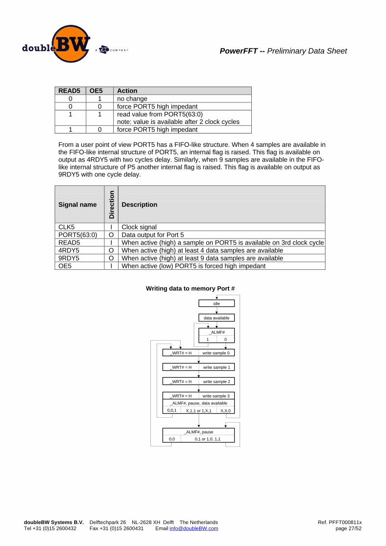
READ5 OE5 Action0 1 no change0 0 force PORT5 high impedant1 1 read value from PORT5(63:0)
note: value is available after 2 clock cycles1 0 force PORT5 high impedant
From a user point of view PORT5 has a FIFO-like structure. When 4 samples are available inthe FIFO-like internal structure of PORT5, an internal flag is raised. This flag is available onoutput as 4RDY5 with two cycles delay. Similarly, when 9 samples are available in the FIFO-like internal structure of P5 another internal flag is raised. This flag is available on output as9RDY5 with one cycle delay.
Signal name
Dir
ecti
on
Description
CLK5 I Clock signalPORT5(63:0) O Data output for Port 5READ5 I When active (high) a sample on PORT5 is available on 3rd clock cycle4RDY5 O When active (high) at least 4 data samples are available9RDY5 O When active (high) at least 9 data samples are availableOE5 I When active (low) PORT5 is forced high impedant
idle
data available
_ALMF#
1 0
Writing data to memory Port #
_WRT# = H write sample 0
_WRT# = H write sample 1
_WRT# = H write sample 2
_WRT# = H write sample 3
_ALMF#, pause, data available
X,1,1 or 1,X,1 X,X,00,0,1
_ALMF#, pause
0,1 or 1,0, 1,10,0

PowerFFT -- Preliminary Data Sheet
doubleBW Systems B.V. Delftechpark 26 NL-2628 XH Delft The Netherlands Ref. PFFT000811xTel +31 (0)15 2600432 Fax +31 (0)15 2600431 Email [email protected] page 28/52
_RD# = H read sample 1
_9RDY#, pause
0,0 or 0,1 or 1,1 1,0
_RD# = L read sample 3
_4RDY#, _9RDY#, pause, memory available
X,1,0,1 X,X,X,01,0,0,1 0,0,0,1 or X,X,1,1
idle
pause
0 1
_4RDY#, _9RDY#
1,0 X,1 0,0
memory available
_9RDY#
0 1
_RD# = H
_RD# = H
_RD# = L read sample 2 _RD# = H read sample 2
_RD# = H read sample 3
_RD# = H
_RD# = H
_RD# = H read sample 0
_RD# = H read sample 1
_RD# = L read sample 2
Reading data from memory Port #
_RD# = H read sample 0
Reading / writing on memory Ports 1 to 4The bi-directional Ports 1 to 4 are equivalent, and will be indicated by Port #. The signal DIR#indicates the direction of PORT#. If DIR# is low upon the upgoing edge of CLKSYS, PORT#will switch to write mode. #. If DIR# is high upon the upgoing edge of CLKSYS, PORT# willswitch to read mode.
From a user point of view PORT# has a FIFO-like structure. The flag mechanisms in write orread mode are similar to the PORT0 or PORT5 flag mechanisms, respectively.

PowerFFT -- Preliminary Data Sheet
doubleBW Systems B.V. Delftechpark 26 NL-2628 XH Delft The Netherlands Ref. PFFT000811xTel +31 (0)15 2600432 Fax +31 (0)15 2600431 Email [email protected] page 29/52
Signal nameM
od
e
Dir
ecti
on
Description
CLKSYS - I Clock signalPORT#(56:0) R O Data output for Port #
W I Data input for Port #WRTRD# R I When active (high) a sample on PORT# is available on 3rd clock cycle
W I When active (high) data on PORT# is writtenALMF4RDY# R O When active (high) at least 4 data samples are available
W O Indicates that PORT# is almost fullZPAD9RDY# R O When active (high) at least 9 data samples are available
W I When active (high) "0" data is writtenDIR# - I When low PORT# is set in write mode
When high PORT# is set in read mode
NOTE 1: In read mode (DIR# high), the signals WRTRD#, ALMF4RDY# and ZPAD9RDY#are also referred to as _RD#, _4RDY#, and _9RDY#, respectively.In write mode (DIR# low), the signals WRTRD#, ALMF4RDY# and ZPAD9RDY# arealso referred to as _WRT#, _ALMF#, and _ZPAD#, respectively.
NOTE 2: In case of Crossbar Switch Input setting CSI2(#,$) (i.e., DEST0 ≠ DEST1), thecontrol signals for Port # and Port $ should be equal and synchronized.
In both read and write mode, Port # is optimized for burst length 4 SDRAM data transfers.When the almost full flag ALMF4RDY# becomes active during data transfer from SDRAM toPort #, the current burst length 4 transfer can be finished. When the ready 4 flag ALMF4RDY#becomes active before a data transfer from Port # to SDRAM, a burst length 4 can betransferred. When the ready 9 flag ZPAD9RDY# also becomes active, a following burst length4 can also be transferred.
WRTRD#
CLKSYS
DIR#
PORT#(56:0)
NO ACTION READ S0 READ S1 READ S2 READ S3 NO ACTION
S0 S1 S2 S3 S0 S1 S2 S3
WRITE S0 WRITE S1 WRITE S2 WRITE S3 NO ACTIONNO ACTION NO ACTIONNO ACTION
minimum 4 cycles

PowerFFT -- Preliminary Data Sheet
doubleBW Systems B.V. Delftechpark 26 NL-2628 XH Delft The Netherlands Ref. PFFT000811xTel +31 (0)15 2600432 Fax +31 (0)15 2600431 Email [email protected] page 30/52
READ5 = H read sample 1
9RDY5, pause
0,0 or 0,1 or 1,1 1,0
READ5 = L read sample 3
4RDY5, 9RDY5, pause, data request
X,1,0,1 X,X,X,01,0,0,1 0,0,0,1 or X,X,1,1
idle
pause
0 1
4RDY5, 9RDY5
1,0 X,1 0,0
data request
9RDY5
0 1
READ5 = H
READ5 = H
READ5 = L read sample 2
READ5 = H read sample 0
READ5 = H read sample 2
READ5 = H read sample 3
READ5 = H
READ5 = H
READ5 = H read sample 0
READ5 = H read sample 1
READ5 = L read sample 2
Reading data from Port 5
READ5
CLK5
OE5
PORT5(63:0)
NO ACTION READ S0 READ S1 READ S2 READ S3 NO ACTION
S0 S1 S2 S3 "Z" "Z"

PowerFFT -- Preliminary Data Sheet
doubleBW Systems B.V. Delftechpark 26 NL-2628 XH Delft The Netherlands Ref. PFFT000811xTel +31 (0)15 2600432 Fax +31 (0)15 2600431 Email [email protected] page 31/52
Control interface specification
PO
RT
#
ADDRESS
PORT0
PORT5
PowerFFT
PROG
PVAL
SYNCF0
SYNC0
SYNCAB
SYNCC
SYNC5
READ5
4RDY5
9RDY5
OE5
WRITE0
ZPAD0
ALMF0
ZPAD9RDY#
ALMF4RDY#
WRTRD#
DIR#
CS#
WE#
CAS#
RAS#
SDRAMbank #S
DR
AM
AD
DR
ES
SG
EN
ER
AT
ION
(4x
) IN
PU
TC
ON
TR
OL
OU
TP
UT
CO
NT
RO
LS
YN
CC
ON
TR
OL
PR
OG
Po
wer
FF
T C
on
tro
lad
dre
ss g
ener
ato
r
Programming examplesIn this section, the programs of the standard FFT functions are summarized. The followingassumptions apply:
• The input clock CLK0 is less than or equal to CLKSYS.• Although it is assumed that on each cycle, a sample is read or written, this is not
necessarily the case. The input / output ports prevent collisions by the control signals.The clock cycles indexed in the clock columns correspond to actual read or write cycles.
• The output clock CLK5 is omitted. The read cycles of Port 5 are always linked to thecorresponding input port (one of the memory ports).
• For the examples, all sequence lengths and dimensions are chosen 1024.

PowerFFT -- Preliminary Data Sheet
doubleBW Systems B.V. Delftechpark 26 NL-2628 XH Delft The Netherlands Ref. PFFT000811xTel +31 (0)15 2600432 Fax +31 (0)15 2600431 Email [email protected] page 32/52
• The rows "REPEAT" indicates repetition of the last instructions on all next sequences.• The action "Empty" means: wait until all sequences are read from the chip.• Each step in the algorithms corresponds to different crossbar switch setting, depicted in
accompanying figures.

PowerFFT -- Preliminary Data Sheet
doubleBW Systems B.V. Delftechpark 26 NL-2628 XH Delft The Netherlands Ref. PFFT000811xTel +31 (0)15 2600432 Fax +31 (0)15 2600431 Email [email protected] page 33/52
Short FFT
Clock Programming Syncs
Action
CL
K0
CL
KS
YS
SET_PROCESSOR_CORE SET_CROSSBAR_SWITCH SET_PORT_CONVERTORS
SY
NC
F0
SY
NC
0
SY
NC
AB
SY
NC
C
SY
NC
5
0 Transparent à FFT CST00() FRMT0 = "00011": FINST = 00 FRMT0 = "00011"
71 EXP5 = "don't care"Init
-1 X X X X X0 0 Transparent à FFT CST00() FRMT0 = "00011": : FINST = 00 FRMT0 = "00011": 71 EXP5 = "don't care"
127 X X X X:
FF
T
1023
REPEAT
0 0 Transparent à FFT CST00() FRMT0 = "00011": : FINST = 00 FRMT0 = "00011": 71 EXP5 = "don't care"
127 X X X X:
FF
T
1023 X0:
Con
tinuo
us 1
K p
oint
FF
T
FF
T
1023
XFFT
A B C
1 2 3 4
50
CST00( )

PowerFFT -- Preliminary Data Sheet
doubleBW Systems B.V. Delftechpark 26 NL-2628 XH Delft The Netherlands Ref. PFFT000811xTel +31 (0)15 2600432 Fax +31 (0)15 2600431 Email [email protected] page 34/52
Short convolution, fixed filter
Clock Programming Syncs
Action
CL
K0
CL
KS
YS
SET_PROCESSOR_CORE SET_CROSSBAR_SWITCH SET_PORT_CONVERTORS
SY
NC
F0
SY
NC
0
SY
NC
AB
SY
NC
C
SY
NC
5
0 Transparent à FFT CST00() FRMT0 = "00011": FINST = 03 FRMT5 = "00011"
71 EXP5 = "don't care"Init
-1 X X X X X0 0 Transparent à FFT CSI0(), CST15(1) FRMT0 = "00011": : FINST = 03 FRMT5 = "00011": 71 EXP5 = "don't care"
127 X X:P
hase
1
10230 Transparent à FFT CST00() FRMT0 = "00011": FINST = 03 FRMT0 = "00011"
71 EXP5 = "don't care":
127 X X X X:P
hase
2
1023 X0 0 Transparent à FFT CSI0(), CST15(1) FRMT0 = "00011": : FINST = 03 FRMT5 = "00011": 71 EXP5 = "don't care"
127 X X:P
hase
1
10230 Transparent à FFT CST00() FRMT0 = "00011": FINST = 03 FRMT0 = "00011"
71 EXP5 = "don't care":
127 X X X X:P
hase
2
1023 X
REPEAT
0 0 Transparent à FFT CSI0(), CST15(1) FRMT0 = "don't care": : FINST = 03 FRMT5 = "don't care": 71 EXP5 = "don't care"
127 X X:P
hase
1
10230 "don't care" "don't care" FRMT0 = "00011": FRMT0 = "00011"
Con
tinuo
us 1
K c
onvo
lutio
n
Pha
se2
1023 EXP5 = "don't care"
XFFT
A B C
1 2 3 4
50
XFFT
A B C
1 2 3 4
50
CST00( )1st phase
CST15(1)2nd phase

PowerFFT -- Preliminary Data Sheet
doubleBW Systems B.V. Delftechpark 26 NL-2628 XH Delft The Netherlands Ref. PFFT000811xTel +31 (0)15 2600432 Fax +31 (0)15 2600431 Email [email protected] page 35/52
Short convolution, updated filter
Clock Programming Syncs
Action
CL
K0
CL
KS
YS
SET_PROCESSOR_CORE SET_CROSSBAR_SWITCH SET_PORT_CONVERTORS
SY
NC
F0
SY
NC
0
SY
NC
AB
SY
NC
C
SY
NC
5
0 Transparent à FFT CST00() FRMT0 = "00011": FINST = 02 FRMT5 = "00011"
71 EXP5 = "don't care"Init
-1 X X X X X0 0 Transparent à FFT CST00() FRMT0 = "00011": : FINST = 02 FRMT5 = "00011": 71 EXP5 = "don't care"
127 X X:P
hase
1
1023 X0 Transparent à FFT CST00() FRMT0 = "00011": FINST = 02 FRMT0 = "00011"
71 EXP5 = "don't care":
127 X X X X:P
hase
2
1023 X0 0 Transparent à FFT CST00() FRMT0 = "00011": : FINST = 02 FRMT5 = "00011": 71 EXP5 = "don't care"
127 X X:P
hase
1
1023 X0 Transparent à FFT CST00() FRMT0 = "00011": FINST = 02 FRMT0 = "00011"
71 EXP5 = "don't care":
127 X X X X:P
hase
2
1023 X
REPEAT
0 0 Transparent à FFT CST15(1) FRMT0 = "don't care": : FINST = 02 FRMT5 = "don't care": 71 EXP5 = "don't care"
127 X X:P
hase
1
1023 X0 "don't care" "don't care" FRMT0 = "00011": FRMT0 = "00011"
Con
tinuo
us 1
K c
onvo
lutio
n
Pha
se2
1023 EXP5 = "don't care"
XFFT
A B C
1 2 3 4
50
XFFT
A B C
1 2 3 4
50
CST00( )1st phase
CST00( )2nd phase

PowerFFT -- Preliminary Data Sheet
doubleBW Systems B.V. Delftechpark 26 NL-2628 XH Delft The Netherlands Ref. PFFT000811xTel +31 (0)15 2600432 Fax +31 (0)15 2600431 Email [email protected] page 36/52
Long FFT
Clock Programming Syncs
Action
CL
K0
CL
KS
YS
SET_PROCESSOR_CORE SET_CROSSBAR_SWITCH SET_PORT_CONVERTORS
SY
NC
F0
SY
NC
0
SY
NC
AB
SY
NC
C
SY
NC
5
0 "don't care" CSI1(1), CST14() FRMT0 = "00011": FRMT5 = " don't care "
71 EXP5 = "don't care"Init
-1 X X X X X0 0 "don't care" CSI1(1), CST14() FRMT0 = "00011": : FRMT5 = " don't care ": 71 EXP5 = "don't care"
127 X X X X::C
orne
r tu
rn
1023 X
REPEAT
0 0 "don't care" CSI1(1), CST14() FRMT0 = "00011": : FRMT5 = " don't care ": 71 EXP5 = "don't care"
127 X X X X::C
orne
r tu
rn
1023 X0:R
ead
from
inpu
t and
sto
re d
ata
in tr
ansp
osed
ord
er
Cor
ner
turn
1023
0 Transparent à FFT CSI0(), CST11(1,2), CSO0() FRMT0 = "don't care": FINST = 00 FRMT5 = " don't care "
71 EXP5 = "don't care"Em
pty
-1 X X X X0 Transparent à FFT CSI0(), CST11(1,2), CSO0() FRMT0 = "don't care": FINST = 00 FRMT5 = " don't care "
71 EXP5 = "don't care":
127 X X X X:R
ow F
FT
1023
REPEAT
0 Transparent à FFT CSI0(), CST11(1,2), CSO0() FRMT0 = "don't care": FINST = 00 FRMT5 = " don't care "
71 EXP5 = "don't care":
127 X X X X:R
ow F
FT
10230:
Row
FF
T
1023
0 Multiply à FFT CSI0(), CST13(2,3,4), CSO0() FRMT0 = "don't care": FINST = 00 FRMT5 = " don't care "
71 EXP5 = "don't care"Em
pty
-1 X X X X0 Multiply à FFT CSI0(), CST13(2,3,4), CSO0() FRMT0 = "don't care": FINST = 00 FRMT5 = " don't care "
71 EXP5 = "don't care":
127 X X X X:
Col
umn
FF
T
1023
REPEAT
0 Multiply à FFT CSI0(), CST13(2,3,4), CSO0() FRMT0 = "don't care": FINST = 00 FRMT5 = " don't care "
71 EXP5 = "don't care":
127 X X X X:
Col
umn
FF
T
10230:
For
war
d 1M
poi
nt F
FT
Col
.F
FT
1023

PowerFFT -- Preliminary Data Sheet
doubleBW Systems B.V. Delftechpark 26 NL-2628 XH Delft The Netherlands Ref. PFFT000811xTel +31 (0)15 2600432 Fax +31 (0)15 2600431 Email [email protected] page 37/52
CONTINUED
0 "don't care" CST04(), CSO1(4) FRMT0 = "don't care": FRMT5 = "00011"
71 EXP5 = "don't care"Em
pty
X X X X0 "don't care" CST04(), CSO1(4) FRMT0 = "don't care": FRMT5 = "00011"
71 EXP5 = "don't care":
127 X X X X:C
orne
r tu
rn
1023
REPEAT
0 "don't care" CST04(), CSO1(4) FRMT0 = "don't care": FRMT5 = "00011"
71 EXP5 = "don't care":
127 X X X X:C
orne
r tu
rn
10230:
Re-
tran
spos
e da
ta a
nd w
rite
to o
utpu
t
Cor
ner
turn
1023
XFFT
A B C
1 2 3 4
50
XFFT
A B C
1 2 3 4
50
XFFT
A B C
1 2 3 4
50
XFFT
A B C
1 2 3 4
50
CSI1(1)
CST13(2,3,4) CSO1(4)
CST11(1,2)

PowerFFT -- Preliminary Data Sheet
doubleBW Systems B.V. Delftechpark 26 NL-2628 XH Delft The Netherlands Ref. PFFT000811xTel +31 (0)15 2600432 Fax +31 (0)15 2600431 Email [email protected] page 38/52
Long convolution, fixed filter
Clock Programming Syncs
Action
CL
K0
CL
KS
YS
SET_PROCESSOR_CORE SET_CROSSBAR_SWITCH SET_PORT_CONVERTORS
SY
NC
F0
SY
NC
0
SY
NC
AB
SY
NC
C
SY
NC
5
0 "don't care" CSI1(1), CST14() FRMT0 = "00011": FRMT5 = " don't care "
71 EXP5 = "don't care"Init
-1 X X X X X0 0 "don't care" CSI1(1), CST14() FRMT0 = "00011": : FRMT5 = " don't care ": 71 EXP5 = "don't care"
127 X X X X::C
orne
r tu
rn
1023 X
REPEAT
0 0 "don't care" CSI1(1), CST14() FRMT0 = "00011": : FRMT5 = " don't care ": 71 EXP5 = "don't care"
127 X X X X::C
orne
r tu
rn
1023 X0:R
ead
from
inpu
t and
sto
re d
ata
in tr
ansp
osed
ord
er
Cor
ner
turn
1023
0 Transparent à FFT CSI0(), CST11(1,2), CSO0() FRMT0 = "don't care": FINST = 00 FRMT5 = " don't care "
71 EXP5 = "don't care"Em
pty
-1 X X X X0 Transparent à FFT CSI0(), CST11(1,2), CSO0() FRMT0 = "don't care": FINST = 00 FRMT5 = " don't care "
71 EXP5 = "don't care":
127 X X X X:R
ow F
FT
1023
REPEAT
0 Transparent à FFT CSI0(), CST11(1,2), CSO0() FRMT0 = "don't care": FINST = 00 FRMT5 = " don't care "
71 EXP5 = "don't care":
127 X X X X:R
ow F
FT
10230:
Row
FF
T
1023
0 Multiply à FFT CSI0(), CST13(2,3,4), CSO0() FRMT0 = "don't care": FINST = 00 FRMT5 = " don't care "
71 EXP5 = "don't care"Em
pty
-1 X X X X0 Multiply à FFT CSI0(), CST13(2,3,4), CSO0() FRMT0 = "don't care": FINST = 00 FRMT5 = " don't care "
71 EXP5 = "don't care":
127 X X X X:
Col
umn
FF
T
1023
REPEAT
0 Multiply à FFT CSI0(), CST13(2,3,4), CSO0() FRMT0 = "don't care": FINST = 00 FRMT5 = " don't care "
71 EXP5 = "don't care":
127 X X X X:
Col
umn
FF
T
10230:
For
war
d 1M
poi
nt F
FT
Col
.F
FT
1023

PowerFFT -- Preliminary Data Sheet
doubleBW Systems B.V. Delftechpark 26 NL-2628 XH Delft The Netherlands Ref. PFFT000811xTel +31 (0)15 2600432 Fax +31 (0)15 2600431 Email [email protected] page 39/52
CONTINUED
0 Multiply à FFT CSI0(), CST13(4,3,2), CSO0() FRMT0 = "don't care": FINST = 01 FRMT5 = " don't care "
71 EXP5 = "don't care"Em
pty
-1 X X X X0 Multiply à FFT CSI0(), CST13(4,3,2), CSO0() FRMT0 = "don't care": FINST = 01 FRMT5 = " don't care "
71 EXP5 = "don't care":
127 X X X X:R
ow IF
FT
1023
REPEAT
0 Multiply à FFT CSI0(), CST13(4,3,2), CSO0() FRMT0 = "don't care": FINST = 01 FRMT5 = " don't care "
71 EXP5 = "don't care":
127 X X X X:R
ow IF
FT
10230:
Row
IFF
T
1023
0 Conj. multiply à FFT CSI0(), CST13(2,3,4), CSO0() FRMT0 = "don't care": FINST = 01 FRMT5 = " don't care "
71 EXP5 = "don't care"Em
pty
-1 X X X X0 Conj. multiply à FFT CSI0(), CST13(2,3,4), CSO0() FRMT0 = "don't care": FINST = 01 FRMT5 = " don't care "
71 EXP5 = "don't care":
127 X X X X:
Col
umn
IFF
T
1023
REPEAT
0 Conj. multiply à FFT CSI0(), CST13(2,3,4), CSO0() FRMT0 = "don't care": FINST = 01 FRMT5 = " don't care "
71 EXP5 = "don't care":
127 X X X X:
Col
umn
FF
T
10230:
Mul
tiply
filte
r sp
ectr
um a
nd in
vers
e 1M
poi
nt F
FT
Col
.IF
FT
1023
0 "don't care" CST04(), CSO1(4) FRMT0 = "don't care": FRMT5 = "00011"
71 EXP5 = "don't care"Em
pty
-1 X X X X0 "don't care" CST04(), CSO1(4) FRMT0 = "don't care": FRMT5 = "00011"
71 EXP5 = "don't care":
127 X X X X:C
orne
r tu
rn
1023
REPEAT
0 "don't care" CST04(), CSO1(4) FRMT0 = "don't care": FRMT5 = "00011"
71 EXP5 = "don't care":
127 X X X X:C
orne
r tu
rn
10230:
Re-
tran
spos
e da
ta a
nd w
rite
to o
utpu
t
Cor
ner
turn
1023

PowerFFT -- Preliminary Data Sheet
doubleBW Systems B.V. Delftechpark 26 NL-2628 XH Delft The Netherlands Ref. PFFT000811xTel +31 (0)15 2600432 Fax +31 (0)15 2600431 Email [email protected] page 40/52
XFFT
A B C
1 2 3 4
50
XFFT
A B C
1 2 3 4
50
XFFT
A B C
1 2 3 4
50
XFFT
A B C
1 2 3 4
50
XFFT
A B C
1 2 3 4
50
XFFT
A B C
1 2 3 4
50
CSI1(1)
CST13(2,3,4) CST13(4,3,2)
CST11(1,2)
CST13(2,3,4) CSO1(4)
PowerFFT -- Preliminary Data Sheet
doubleBW Systems B.V. Delftechpark 26 NL-2628 XH Delft The Netherlands Ref. PFFT000811xTel +31 (0)15 2600432 Fax +31 (0)15 2600431 Email [email protected] page 41/52
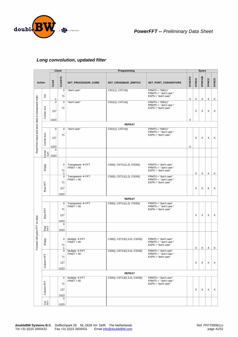
Long convolution, updated filter
Clock Programming Syncs
Action
CL
K0
CL
KS
YS
SET_PROCESSOR_CORE SET_CROSSBAR_SWITCH SET_PORT_CONVERTORS
SY
NC
F0
SY
NC
0
SY
NC
AB
SY
NC
C
SY
NC
5
0 "don't care" CSI1(1), CST14() FRMT0 = "00011": FRMT5 = " don't care "
71 EXP5 = "don't care"Init
-1 X X X X X0 0 "don't care" CSI1(1), CST14() FRMT0 = "00011": : FRMT5 = " don't care ": 71 EXP5 = "don't care"
127 X X X X::C
orne
r tu
rn
1023 X
REPEAT
0 0 "don't care" CSI1(1), CST14() FRMT0 = "00011": : FRMT5 = " don't care ": 71 EXP5 = "don't care"
127 X X X X::C
orne
r tu
rn
1023 X0:R
ead
from
inpu
t and
sto
re d
ata
in tr
ansp
osed
ord
er
Cor
ner
turn
1023
0 Transparent à FFT CSI0(), CST11(1,2), CSO0() FRMT0 = "don't care": FINST = 00 FRMT5 = " don't care "
71 EXP5 = "don't care"Em
pty
-1 X X X X0 Transparent à FFT CSI0(), CST11(1,2), CSO0() FRMT0 = "don't care": FINST = 00 FRMT5 = " don't care "
71 EXP5 = "don't care":
127 X X X X:R
ow F
FT
1023
REPEAT
0 Transparent à FFT CSI0(), CST11(1,2), CSO0() FRMT0 = "don't care": FINST = 00 FRMT5 = " don't care "
71 EXP5 = "don't care":
127 X X X X:R
ow F
FT
10230:
Row
FF
T
1023
0 Multiply à FFT CSI0(), CST13(2,3,4), CSO0() FRMT0 = "don't care": FINST = 00 FRMT5 = " don't care "
71 EXP5 = "don't care"Em
pty
-1 X X X X0 Multiply à FFT CSI0(), CST13(2,3,4), CSO0() FRMT0 = "don't care": FINST = 00 FRMT5 = " don't care "
71 EXP5 = "don't care":
127 X X X X:
Col
umn
FF
T
1023
REPEAT
0 Multiply à FFT CSI0(), CST13(2,3,4), CSO0() FRMT0 = "don't care": FINST = 00 FRMT5 = " don't care "
71 EXP5 = "don't care":
127 X X X X:
Col
umn
FF
T
10230:
For
war
d 1M
poi
nt F
FT
on
data
Col
.F
FT
1023

PowerFFT -- Preliminary Data Sheet
doubleBW Systems B.V. Delftechpark 26 NL-2628 XH Delft The Netherlands Ref. PFFT000811xTel +31 (0)15 2600432 Fax +31 (0)15 2600431 Email [email protected] page 42/52
CONTINUED0 "don't care" CSI1(1), CST14() FRMT0 = "00011": FRMT5 = " don't care "
71 EXP5 = "don't care"Init
-1 X X X X X0 0 "don't care" CSI1(1), CST14() FRMT0 = "00011": : FRMT5 = " don't care ": 71 EXP5 = "don't care"
127 X X X X::C
orne
r tu
rn
1023 X
REPEAT
0 0 "don't care" CSI1(1), CST14() FRMT0 = "00011": : FRMT5 = " don't care ": 71 EXP5 = "don't care"
127 X X X X::C
orne
r tu
rn
1023 X0:R
ead
from
inpu
t and
sto
re fi
lter
in tr
ansp
osed
ord
er
Cor
ner
turn
1023
0 Transparent à FFT CSI0(), CST11(1,2), CSO0() FRMT0 = "don't care": FINST = 00 FRMT5 = " don't care "
71 EXP5 = "don't care"Em
pty
-1 X X X X0 Transparent à FFT CSI0(), CST11(1,2), CSO0() FRMT0 = "don't care": FINST = 00 FRMT5 = " don't care "
71 EXP5 = "don't care":
127 X X X X:R
ow F
FT
1023
REPEAT
0 Transparent à FFT CSI0(), CST11(1,2), CSO0() FRMT0 = "don't care": FINST = 00 FRMT5 = " don't care "
71 EXP5 = "don't care":
127 X X X X:R
ow F
FT
10230:
Row
FF
T
1023
0 Multiply à FFT CSI0(), CST13(2,3,1), CSO0() FRMT0 = "don't care": FINST = 00 FRMT5 = " don't care "
71 EXP5 = "don't care"Em
pty
-1 X X X X0 Multiply à FFT CSI0(), CST13(2,3,1), CSO0() FRMT0 = "don't care": FINST = 00 FRMT5 = " don't care "
71 EXP5 = "don't care":
127 X X X X:
Col
umn
FF
T
1023
REPEAT
0 Multiply à FFT CSI0(), CST13(2,3,1), CSO0() FRMT0 = "don't care": FINST = 00 FRMT5 = " don't care "
71 EXP5 = "don't care":
127 X X X X:
Col
umn
FF
T
10230:
For
war
d 1M
poi
nt F
FT
on
filte
r
Col
.F
FT
1023

PowerFFT -- Preliminary Data Sheet
doubleBW Systems B.V. Delftechpark 26 NL-2628 XH Delft The Netherlands Ref. PFFT000811xTel +31 (0)15 2600432 Fax +31 (0)15 2600431 Email [email protected] page 43/52
CONTINUED
0 Multiply à FFT CSI0(), CST13(1,4,2), CSO0() FRMT0 = "don't care": FINST = 01 FRMT5 = " don't care "
71 EXP5 = "don't care"Em
pty
-1 X X X X0 Multiply à FFT CSI0(), CST13(1,4,2), CSO0() FRMT0 = "don't care": FINST = 01 FRMT5 = " don't care "
71 EXP5 = "don't care":
127 X X X X:R
ow IF
FT
1023
REPEAT
0 Multiply à FFT CSI0(), CST13(1,4,2), CSO0() FRMT0 = "don't care": FINST = 01 FRMT5 = " don't care "
71 EXP5 = "don't care":
127 X X X X:R
ow IF
FT
10230:
Row
IFF
T
1023
0 Conj. multiply à FFT CSI0(), CST13(2,3,4), CSO0() FRMT0 = "don't care": FINST = 01 FRMT5 = " don't care "
71 EXP5 = "don't care"Em
pty
-1 X X X X0 Conj. multiply à FFT CSI0(), CST13(2,3,4), CSO0() FRMT0 = "don't care": FINST = 01 FRMT5 = " don't care "
71 EXP5 = "don't care":
127 X X X X:
Col
umn
IFF
T
1023
REPEAT
0 Conj. multiply à FFT CSI0(), CST13(2,3,4), CSO0() FRMT0 = "don't care": FINST = 01 FRMT5 = " don't care "
71 EXP5 = "don't care":
127 X X X X:
Col
umn
FF
T
10230:
Mul
tiply
filte
r sp
ectr
um a
nd in
vers
e 1M
poi
nt F
FT
Col
.IF
FT
1023
0 "don't care" CST04(), CSO1(4) FRMT0 = "don't care": FRMT5 = "00011"
71 EXP5 = "don't care"Em
pty
-1 X X X X0 "don't care" CST04(), CSO1(4) FRMT0 = "don't care": FRMT5 = "00011"
71 EXP5 = "don't care":
127 X X X X:C
orne
r tu
rn
1023
REPEAT
0 "don't care" CST04(), CSO1(4) FRMT0 = "don't care": FRMT5 = "00011"
71 EXP5 = "don't care"
X X X X
Cor
ner
turn
Re-
tran
spos
e da
ta a
nd w
rite
to o
utpu
t
Cor
ner
turn

PowerFFT -- Preliminary Data Sheet
doubleBW Systems B.V. Delftechpark 26 NL-2628 XH Delft The Netherlands Ref. PFFT000811xTel +31 (0)15 2600432 Fax +31 (0)15 2600431 Email [email protected] page 44/52
XFFT
A B C
1 2 3 4
50
XFFT
A B C
1 2 3 4
50
XFFT
A B C
1 2 3 4
50
XFFT
A B C
1 2 3 4
50
XFFT
A B C
1 2 3 4
50
XFFT
A B C
1 2 3 4
50
XFFT
A B C
1 2 3 4
50
XFFT
A B C
1 2 3 4
50
XFFT
A B C
1 2 3 4
50
CSI1(1)
CST13(2,3,4) CSI1(1)
CST11(1,2)
CST11(1,2) CST13(2,3,1)
CST13(1,4,2) CST13(2,3,4)
CSO1(4)

PowerFFT -- Preliminary Data Sheet
doubleBW Systems B.V. Delftechpark 26 NL-2628 XH Delft The Netherlands Ref. PFFT000811xTel +31 (0)15 2600432 Fax +31 (0)15 2600431 Email [email protected] page 45/52
2D FFT
Clock Programming Syncs
Action
CL
K0
CL
KS
YS
SET_PROCESSOR_CORE SET_CROSSBAR_SWITCH SET_PORT_CONVERTORS
SY
NC
F0
SY
NC
0
SY
NC
AB
SY
NC
C
SY
NC
5
0 Transparent à FFT CST05(1), CSO0() FRMT0 = "00011": FINST = 00 FRMT5 = " don't care "
71 EXP5 = "don't care"-1 X X X X X0 Transparent à FFT CST05(1), CSO0() FRMT0 = "00011": FINST = 00 FRMT5 = " don't care "
71 EXP5 = "don't care":
127 X X X X:R
ow F
FT
1023 X
REPEAT
0 Transparent à FFT CST05(1), CSO0() FRMT0 = "00011": FINST = 00 FRMT5 = " don't care "
71 EXP5 = "don't care":
127 X X X X:R
ow F
FT
1023 X0:
Row
dim
ensi
on 1
K p
oint
FF
T
Row
FF
T
1023
0 Transparent à FFT CSI0(), CST11(1,2), CSO0() FRMT0 = "don't care": FINST = 00 FRMT5 = " don't care "
71 EXP5 = "don't care"Em
pty
-1 X X X X0 Transparent à FFT CSI0(), CST11(1,2), CSO0() FRMT0 = "don't care": FINST = 00 FRMT5 = " don't care "
71 EXP5 = "don't care":
127 X X X X:
Col
umn
FF
T
1023
REPEAT
0 Transparent à FFT CSI0(), CST11(1,2), CSO0() FRMT0 = "don't care": FINST = 00 FRMT5 = " don't care "
71 EXP5 = "don't care":
127 X X X X:
Col
umn
FF
T
10230:
Col
umn
dim
ensi
on 1
K p
oint
FF
T
Col
.F
FT
1023
0 "don't care" CST04(), CSO1(2) FRMT0 = "don't care": FRMT5 = "00011"
71 EXP5 = "don't care"Em
pty
-1 X X X X0 "don't care" CST04(), CSO1(2) FRMT0 = "don't care": FRMT5 = "00011"
71 EXP5 = "don't care":
127 X X X X:C
orne
r tu
rn
1023
REPEAT
0 "don't care" CST04(), CSO1(2) FRMT0 = "don't care": FRMT5 = "00011"
71 EXP5 = "don't care":
127 X X X X:C
orne
r tu
rn
10230:
Re-
tran
spos
e da
ta a
nd w
rite
to o
utpu
t
Cor
ner
turn
1023
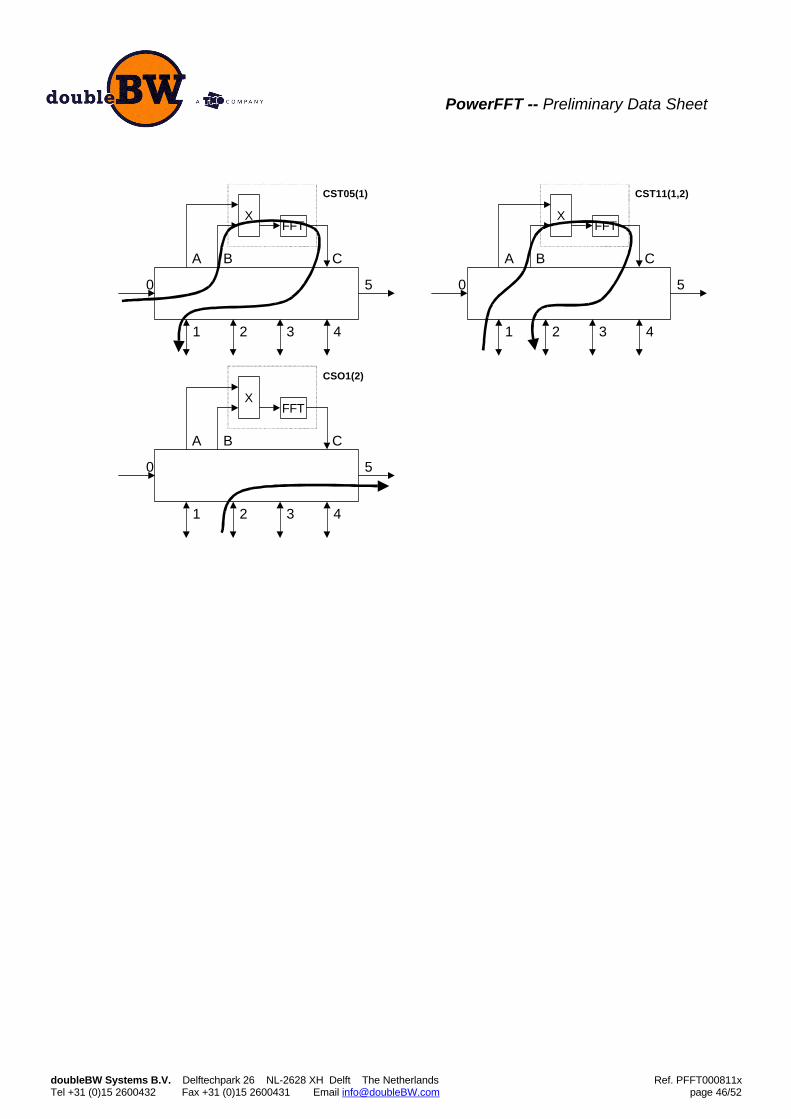
PowerFFT -- Preliminary Data Sheet
doubleBW Systems B.V. Delftechpark 26 NL-2628 XH Delft The Netherlands Ref. PFFT000811xTel +31 (0)15 2600432 Fax +31 (0)15 2600431 Email [email protected] page 46/52
XFFT
A B C
1 2 3 4
50
XFFT
A B C
1 2 3 4
50
XFFT
A B C
1 2 3 4
50
CST05(1)
CSO1(2)
CST11(1,2)

PowerFFT -- Preliminary Data Sheet
doubleBW Systems B.V. Delftechpark 26 NL-2628 XH Delft The Netherlands Ref. PFFT000811xTel +31 (0)15 2600432 Fax +31 (0)15 2600431 Email [email protected] page 47/52
2D convolution, fixed filter
Clock Programming Syncs
Action
CL
K0
CL
KS
YS
SET_PROCESSOR_CORE SET_CROSSBAR_SWITCH SET_PORT_CONVERTORS
SY
NC
F0
SY
NC
0
SY
NC
AB
SY
NC
C
SY
NC
5
0 Transparent à FFT CST05(1), CSO0() FRMT0 = "00011": FINST = 00 FRMT5 = " don't care "
71 EXP5 = "don't care"-1 X X X X X0 Transparent à FFT CST05(1), CSO0() FRMT0 = "00011": FINST = 00 FRMT5 = " don't care "
71 EXP5 = "don't care":
127 X X X X:R
ow F
FT
1023 X
REPEAT
0 Transparent à FFT CST05(1), CSO0() FRMT0 = "00011": FINST = 00 FRMT5 = " don't care "
71 EXP5 = "don't care":
127 X X X X:R
ow F
FT
1023 X0:
Row
dim
ensi
on fo
rwar
d F
FT
Row
FF
T
1023
0 Transparent à FFT CSI0(), CST11(1,2), CSO0() FRMT0 = "don't care": FINST = 00 FRMT5 = " don't care "
71 EXP5 = "don't care"Em
pty
-1 X X X X0 Transparent à FFT CSI0(), CST11(1,2), CSO0() FRMT0 = "don't care": FINST = 00 FRMT5 = " don't care "
71 EXP5 = "don't care":
127 X X X X:
Col
umn
FF
T
1023
REPEAT
0 Transparent à FFT CSI0(), CST11(1,2), CSO0() FRMT0 = "don't care": FINST = 00 FRMT5 = " don't care "
71 EXP5 = "don't care":
127 X X X X:
Col
umn
FF
T
10230:
Col
umn
dim
ensi
on fo
rwar
d F
FT
Col
.F
FT
1023
0 Multiply à FFT CSI0(), CST13(2,3,4), CSO0() FRMT0 = "don't care": FINST = 01 FRMT5 = " don't care "
71 EXP5 = "don't care"Em
pty
-1 X X X X0 Multiply à FFT CSI0(), CST13(2,3,4), CSO0() FRMT0 = "don't care": FINST = 01 FRMT5 = " don't care "
71 EXP5 = "don't care":
127 X X X X:
Col
umn
IFF
T
1023
REPEAT
0 Multiply à FFT CSI0(), CST13(2,3,4), CSO0() FRMT0 = "don't care": FINST = 01 FRMT5 = " don't care "
71 EXP5 = "don't care":
127 X X X X:
Col
umn
IFF
T
10230:M
ultip
ly fi
lter
spec
trum
and
col
umn
dim
ensi
on !K
poi
nt IF
FT
Col
.IF
FT
1023

PowerFFT -- Preliminary Data Sheet
doubleBW Systems B.V. Delftechpark 26 NL-2628 XH Delft The Netherlands Ref. PFFT000811xTel +31 (0)15 2600432 Fax +31 (0)15 2600431 Email [email protected] page 48/52
CONTINUED
0 Transparent à FFT CSI0(), CST15(4) FRMT0 = "don't care": FINST = 01 FRMT5 = "00011"
71 EXP5 = "don't care"Em
pty
-1 X X X X0 Transparent à FFT CSI0(), CST15(4) FRMT0 = "don't care": FINST = 01 FRMT5 = "00011"
71 EXP5 = "don't care":
127 X X X X:R
ow IF
FT
1023
REPEAT
0 Transparent à FFT CSI0(), CST15(4) FRMT0 = "don't care": FINST = 01 FRMT5 = "00011"
71 EXP5 = "don't care":
127 X X X X:R
ow IF
FT
10230:
Row
dim
ensi
on fo
rwar
d F
FT
and
writ
e ou
tput
dat
a
Row
IFF
T
1023
XFFT
A B C
1 2 3 4
50
XFFT
A B C
1 2 3 4
50
XFFT
A B C
1 2 3 4
50
XFFT
A B C
1 2 3 4
50
CST05(1)
CST13(2,3,4) CST15(4)
CST11(1,2)

PowerFFT -- Preliminary Data Sheet
doubleBW Systems B.V. Delftechpark 26 NL-2628 XH Delft The Netherlands Ref. PFFT000811xTel +31 (0)15 2600432 Fax +31 (0)15 2600431 Email [email protected] page 49/52
2D convolution, updated filter
Clock Programming Syncs
Action
CL
K0
CL
KS
YS
SET_PROCESSOR_CORE SET_CROSSBAR_SWITCH SET_PORT_CONVERTORS
SY
NC
F0
SY
NC
0
SY
NC
AB
SY
NC
C
SY
NC
5
0 Transparent à FFT CST05(1), CSO0() FRMT0 = "00011": FINST = 00 FRMT5 = " don't care "
71 EXP5 = "don't care"-1 X X X X X0 Transparent à FFT CST05(1), CSO0() FRMT0 = "00011": FINST = 00 FRMT5 = " don't care "
71 EXP5 = "don't care":
127 X X X X:R
ow F
FT
1023 X
REPEAT
0 Transparent à FFT CST05(1), CSO0() FRMT0 = "00011": FINST = 00 FRMT5 = " don't care "
71 EXP5 = "don't care":
127 X X X X:R
ow F
FT
1023 X0:
Row
dim
ensi
on fo
rwar
d F
FT
on
data
Row
FF
T
1023
0 Transparent à FFT CSI0(), CST11(1,2), CSO0() FRMT0 = "don't care": FINST = 00 FRMT5 = " don't care "
71 EXP5 = "don't care"Em
pty
-1 X X X X0 Transparent à FFT CSI0(), CST11(1,2), CSO0() FRMT0 = "don't care": FINST = 00 FRMT5 = " don't care "
71 EXP5 = "don't care":
127 X X X X:
Col
umn
FF
T
1023
REPEAT
0 Transparent à FFT CSI0(), CST11(1,2), CSO0() FRMT0 = "don't care": FINST = 00 FRMT5 = " don't care "
71 EXP5 = "don't care":
127 X X X X:
Col
umn
FF
T
10230:
Col
umn
dim
ensi
on fo
rwar
d F
FT
on
data
Col
.F
FT
1023
0 Transparent à FFT CST05(1), CSO0() FRMT0 = "00011": FINST = 00 FRMT5 = " don't care "
71 EXP5 = "don't care"Em
pty
-1 X X X X X0 Transparent à FFT CST05(1), CSO0() FRMT0 = "00011": FINST = 00 FRMT5 = " don't care "
71 EXP5 = "don't care":
127 X X X X:R
ow F
FT
1023 X
REPEAT
0 Transparent à FFT CST05(1), CSO0() FRMT0 = "00011": FINST = 00 FRMT5 = " don't care "
71 EXP5 = "don't care":
127 X X X X:R
ow F
FT
1023 X0:
Row
dim
ensi
on fo
rwar
d F
FT
on
filte
r
Row
FF
T
1023
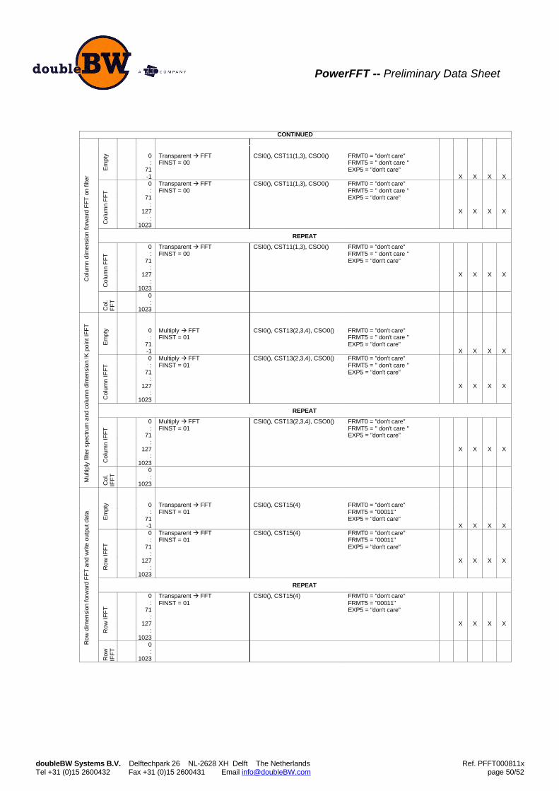
PowerFFT -- Preliminary Data Sheet
doubleBW Systems B.V. Delftechpark 26 NL-2628 XH Delft The Netherlands Ref. PFFT000811xTel +31 (0)15 2600432 Fax +31 (0)15 2600431 Email [email protected] page 50/52
CONTINUED
0 Transparent à FFT CSI0(), CST11(1,3), CSO0() FRMT0 = "don't care": FINST = 00 FRMT5 = " don't care "
71 EXP5 = "don't care"Em
pty
-1 X X X X0 Transparent à FFT CSI0(), CST11(1,3), CSO0() FRMT0 = "don't care": FINST = 00 FRMT5 = " don't care "
71 EXP5 = "don't care":
127 X X X X:
Col
umn
FF
T
1023
REPEAT
0 Transparent à FFT CSI0(), CST11(1,3), CSO0() FRMT0 = "don't care": FINST = 00 FRMT5 = " don't care "
71 EXP5 = "don't care":
127 X X X X:
Col
umn
FF
T
10230:
Col
umn
dim
ensi
on fo
rwar
d F
FT
on
filte
r
Col
.F
FT
1023
0 Multiply à FFT CSI0(), CST13(2,3,4), CSO0() FRMT0 = "don't care": FINST = 01 FRMT5 = " don't care "
71 EXP5 = "don't care"Em
pty
-1 X X X X0 Multiply à FFT CSI0(), CST13(2,3,4), CSO0() FRMT0 = "don't care": FINST = 01 FRMT5 = " don't care "
71 EXP5 = "don't care":
127 X X X X:
Col
umn
IFF
T
1023
REPEAT
0 Multiply à FFT CSI0(), CST13(2,3,4), CSO0() FRMT0 = "don't care": FINST = 01 FRMT5 = " don't care "
71 EXP5 = "don't care":
127 X X X X:
Col
umn
IFF
T
10230:M
ultip
ly fi
lter
spec
trum
and
col
umn
dim
ensi
on !K
poi
nt IF
FT
Col
.IF
FT
1023
0 Transparent à FFT CSI0(), CST15(4) FRMT0 = "don't care": FINST = 01 FRMT5 = "00011"
71 EXP5 = "don't care"Em
pty
-1 X X X X0 Transparent à FFT CSI0(), CST15(4) FRMT0 = "don't care": FINST = 01 FRMT5 = "00011"
71 EXP5 = "don't care":
127 X X X X:R
ow IF
FT
1023
REPEAT
0 Transparent à FFT CSI0(), CST15(4) FRMT0 = "don't care": FINST = 01 FRMT5 = "00011"
71 EXP5 = "don't care":
127 X X X X:R
ow IF
FT
10230:
Row
dim
ensi
on fo
rwar
d F
FT
and
writ
e ou
tput
dat
a
Row
IFF
T
1023

PowerFFT -- Preliminary Data Sheet
doubleBW Systems B.V. Delftechpark 26 NL-2628 XH Delft The Netherlands Ref. PFFT000811xTel +31 (0)15 2600432 Fax +31 (0)15 2600431 Email [email protected] page 51/52
XFFT
A B C
1 2 3 4
50
XFFT
A B C
1 2 3 4
50
XFFT
A B C
1 2 3 4
50
XFFT
A B C
1 2 3 4
50
XFFT
A B C
1 2 3 4
50
XFFT
A B C
1 2 3 4
50
CST05(1)
CST05(1) CST11(1,3)
CST11(1,2)
CST13(2,3,4) CST15(4)

PowerFFT -- Preliminary Data Sheet
doubleBW Systems B.V. Delftechpark 26 NL-2628 XH Delft The Netherlands Ref. PFFT000811xTel +31 (0)15 2600432 Fax +31 (0)15 2600431 Email [email protected] page 52/52
Special examplesIn this section, some special combinations of the above standard functions, in combination withinput and output functions are summarized.