powerpoint presentation · • fg controls a linear attenuation block going from 0.5 to 1 • since...
TRANSCRIPT

27.04.2016
APA, SHU, LCO, MAC, ROR

Current Sensors
Programming & Calibration

Calibration Overview
No calibration Blind Calibration
Frontend (sensor-level) Calibration Backend (MCU-level) Calibration PTC mode MUST mode
Hardware none PTC-04, sensor-specific DB MCU
Accuracy ≈5% 0.1% ADC resolution
Pros plug & play factory TC
calibration
accurate analog output
only 3 wires
accurate analog output
VDD=5V
no specific HW factory TC calibration
Cons
magnetic design low absolute
accuracy
VDD increases to 8V change from factory
calib
4-wires change from factory
calib
magnetic design should match sensor sensitivity
Sensors ALL ALL 91208/09 91216/17
ALL

Blind calibration

Concept
• The sensitivity of each Sensor is individually factory calibrated, using 2 EEPROM parameters RG and FG (RoughGain, FineGain), to reach the target sensitivity, as defined in the datasheet.
Blind calibration consists in recalibrating parts without performing measurements: • To do so, it is needed to read and manually change the RG and FG values in the EEPROM. • These 2 parameters codes for the amplification chain that amplify the signal from the hall
plates. • Modifying RG, FG allow to change the output sensitivity of a sensor.
Note : Blind calibration is not available for 91206/07 because the TC parameters need to be re-trim when RG/FG are changed. See slide 23 for more details.

Typical gains and sensitivities
• RG controls a non-linear amplification block • FG controls a linear attenuation block going from 0.5 to 1
• Since all sensors are intrinsically different, the RG and FG values needed to
reach the target sensitivity are different from one sensor to the other . However it is possible to relate RG/FG combination to typical sensitivities:

Blind calibration flow: Example
A sensor 91208CAH (S= 100mV/mT) needs to be recalibrated to 120mV/mT. (i.e. 120% of the actual sensitivity) 1) Extraction of RG, FG values from the EEPROM Results for this specific sensor: RG=3, FG=768 The actual amplification gain is:
𝐺 = 𝐺𝑟𝑔 ∗ 𝐺𝑓𝑔 = 9 ∗ 0.5 +1 − 0.5
1023 − 0∗ 768 − 0 = 7.88
2) RG/FG have to be redefined to get a gain of G = 120%*7.88 = 9.46 We choose: • RG=4 → 𝐺𝑟𝑔= 12.25
• 𝐺𝑓𝑔 =𝐺
𝐺𝑟𝑔=
9.46
12.25= 0.772 → 𝐹𝐺 =
0.772−0.5
0.5∗ 1023 = 557
• RG = 4, FG = 557
FG controls a linear attenuator

Front-end (sensor level) Calibration

Hardware Structure
Melexis PTC04:
Universal Programmer for Melexis sensors calibration
Sensor-specific Daughter-Board (DB):
Interface between PTC04 and application connector
Daughter Board Compatible Current Sensors
PTC04-DB-HALL02 MLX91205
PTC04-DB-HALL03 MLX91206/07
PTC04-DB-HALL05 MLX91210 MLX91208/09 MLX91216/17
PTC04-DB-34103 MLX91220
1 8
9 15
Application connector

Software structure
Application level (high level)
Hardware level (low level)
User Interface Melexis Programming Toolbox
Customer Application
Labview Demo
DLL Layer
PSF PTC04 (general)
PSF MLX Sensor
PSF 91206
General
Advanced
Solver
FIR PTC04 FIR MLX Sensor
FIR 91206

Setup
PC
MLX PTC-04 + Sensor specific DB
USB/RS232
Sensor in application
Software in Labview, C/C++, Python, VB, etc.
3-wire or 4-wire
PTC or MUST mode*
*To be selected in PSF/UI settings

PTC Communication Mode
I. PTC MODE (3-wire) communication: Supply during communication: VDD=8V bi-directional communication on OUT line Available for: all current sensors families
All unused pins can be connected to GND for better EMC and ESD performance
PTC-04
DB
VDD
OUT
GND
MLX_Sensor
Module
Connector Connector
C1: 100nF C2: 10nF C3: 47nF
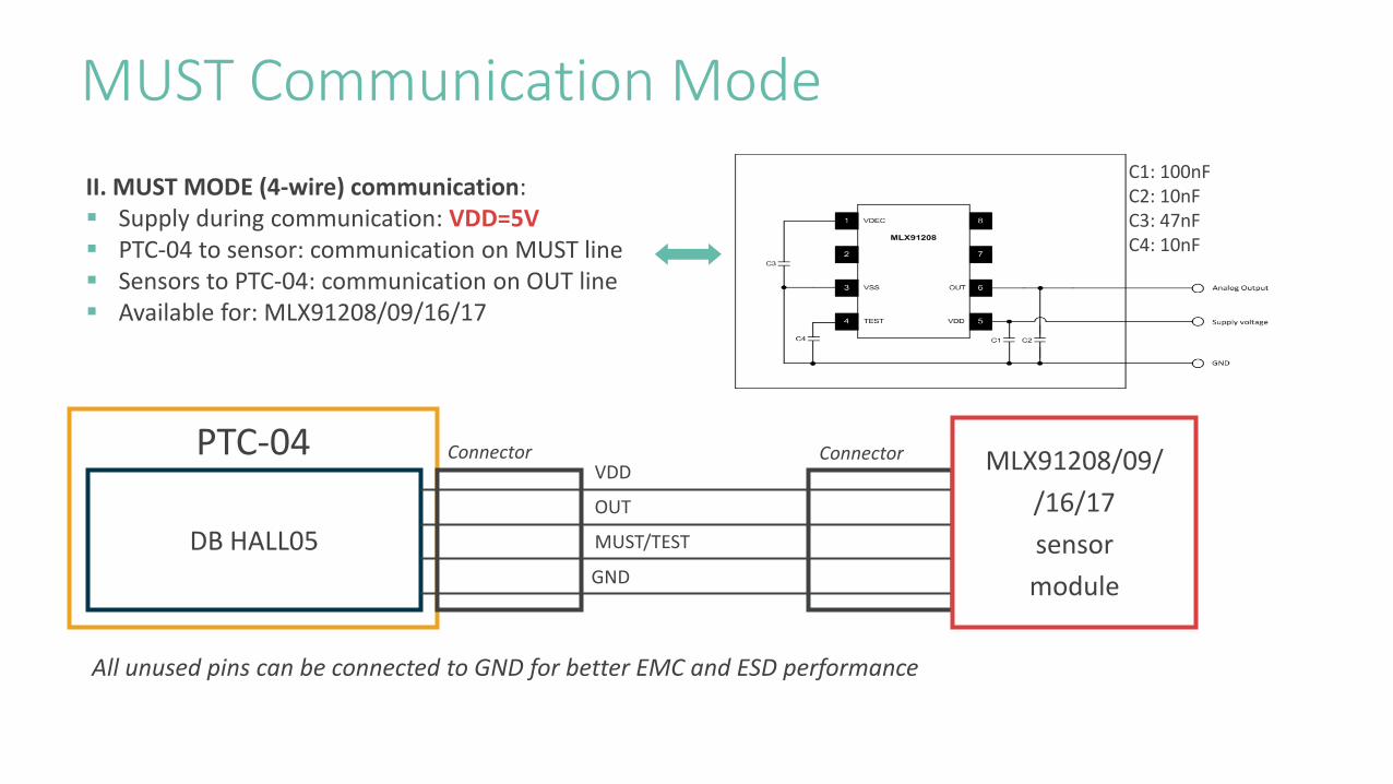
MUST Communication Mode
II. MUST MODE (4-wire) communication: Supply during communication: VDD=5V PTC-04 to sensor: communication on MUST line Sensors to PTC-04: communication on OUT line Available for: MLX91208/09/16/17
PTC-04
DB HALL05
VDD
OUT
MUST/TEST
GND
MLX91208/09/
/16/17
sensor
module
Connector Connector
C1: 100nF C2: 10nF C3: 47nF C4: 10nF
All unused pins can be connected to GND for better EMC and ESD performance

Calibration Log Before starting the Calibration Flow
By default, the option“Do not log to file” is ticked
Optional: Keep a copy of Calibration measures, steps, calculations

User interface
Solver
show/edit memory content
monitor sensor output
check binary memory content
edit general settings
multiple device selector

Multiple Devices
The software can store EEPROM information for up to 16 devices simultaneously. Each device can be selected/enabled with the device selector. However, only 1 device can be physically connected to the OUT1 line of the PTC04. An external hardware switch is required for this purpose. The solver will ask the user to switch between the devices at each step of the calibration process.
During communication, the current consumption increases significantly (short spikes/bursts). The default Idd limit of 100mA is sufficient for 2-3 devices only. For instance, a limit of 300mA is required for 8 devices (multi-socket).

Multiple Devices Dual Die Configuration
PTC-04
DB HALL05
VDD
OUT1
MUST1*
GND
Connector Connector
*The MUST pins are only required for MUST mode communication.
OUT2
MUST2*
MLX91216/7
Sensor module
MLX91216/7
The “Use Double Dies” option in the “Settings” window allows to connect 2 devices to the PTC04 simultaneously. When this option is selected, “Device 1” is on OUT1 and “Device 2” is on OUT2.

Settings
voltage level for «PtcMode» programming
nominal chip supply (Vdd)
select programming mode: PtcModeSupply: use Vdd=8V to put chip in
communication mode MUSTMode: use MUST/test pin to communicate (at
nominal Vdd)
limit for PTC supply current (increase to supply several devices in parallel)
Some of the most important settings are described here.
program two devices in parallel on OUT1 and OUT2

0-Max Solver
Concept: The solver starts from the preset gain and, if required, it sweeps through all allowed RG settings (max. +/-1 for 91206/07) Two reference positions are needed for offset and gain parameters calibration 1) Zero field/current 2) Positive reference field/current
High accuracy for offset trimming
Position 2
More sensitive to hysteresis and saturation
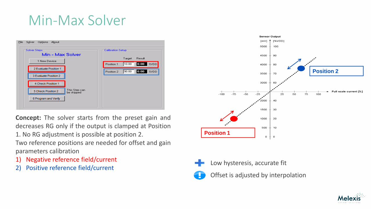
Min-Max Solver
Concept: The solver starts from the preset gain and decreases RG only if the output is clamped at Position 1. No RG adjustment is possible at position 2. Two reference positions are needed for offset and gain parameters calibration 1) Negative reference field/current 2) Positive reference field/current
Position 2
Position 1
Low hysteresis, accurate fit
Offset is adjusted by interpolation

Measurements window
This window allows to monitor sensor supply and output. It is good practice to check that VDD and IDD are in the expected range before starting to program the sensor.
measure by RAM program RAM with values from the TEMP register, then measure output
measure by ROM reset device to program RAM with EEPROM values, then measure output
measure OUT perform single measurement

EEPROM window
To change the value of one or several EEPROM parameter(s), always perform the following steps: → read EEPROM to Image → copy Image to Temp → edit the Temp value(s) → program EEPROM with Temp → read EEPROM and verify The final verification step is required to readback the updated CRC code.

MLX91206 TC Particularity For MLX91206 only, the temperature compensation parameters TC1, TC2COLD, TC2HOT, OFFDRIFT COLD &
HOT are re-trimmed when the gain (RG, FG) is changed in the application.
1) During Final Test Find optimal TC parameters for RG nominal,
RG+1 and RG-1 Store optimal TC parameters for nominal RG
in EEPROM Store “delta TC” parameters for RG+1 and
RG-1 in unused EEPROM bits
2) During EOL Front-End Calibration Find optimal gain settings based on applied
field/current If RG and/or FG has changed: correct TC parameters
for new gain settings based on “delta TC” parameters and look-up tables built based on the Final Test results
Note: the algorithm is based on relative gain/TC changes, therefore it will not work correctly if someone manually changes gain or TC between steps 1 and 2. If a setting is manually changed at any stage, the complete calibration is lost.

Back-end (MCU level) Calibration

MCU Correction Concept
Best Suited for: multi-sensors applications, i.e. on power distribution units, where typically 12 to 24 sensors are on the same PCB in order to monitor the current of each channel.
The concept : assemble the factory-calibrated sensors on each channel apply a reference current (for which a precise output is targeted) on each channel and store the
output of each sensor compare the obtained output to the reference one and calculate the required corrective factor store and apply the corrective factor in the MCU
All Melexis current sensors are already factory-calibrated over temperature!

We Engineer The Sustainable Future