practical test strategies for your smartphone and tablet
TRANSCRIPT
Practical Test Strategies for Your Smartphone and Tablet Memories
Mobile Forum – Santa Clara, CA
By : Cecil Ho, CST, Inc.
[email protected] 972-241-2662Copyright © 2013 CST, Inc.

Memories in your Smartphone and Tablet
LPDDR RAMs with Non-volatile Flash chips, with eMMC or UFS chips
Package format: MCP, POP, External SD Card

The Popular Looks
POP-LPDDR2
MCP-LPDDR2/eMMC
MCP-LPDDR/eMMC
LPDDR3
DDR RAW NAND

New POP Mount Examples
Snapdragon 4 Processor Hidden Under POP DRAM Package
Elpida LPDDR2 DRAM Covers TI Application Processor

Who’s involved with these memories?
• Memory chip integrators• Original memory chip vendors• Packaging house• Equipment Manufacturers• Subcontract Assemblersfor: handsets, tablet computer, e-
reader, camera, games……

Memory Packages Are Semi-custom
• Although JEDEC publish MCP pinout diagrams, electrical feature and function varies.
• Combination option also varies.different LPDRAM generationsdifferent internal density stacksdifferent number of channelsdifferent proprietary features

Similar Pinout, yet Different
LPDDR2/ Flash combo have different pinout from each vendor

Possible Mobile Memory System Configurations
Mobile Memories are Difficult to Test
• DRAM - Hi frequency and high performance testing fixture involves in signal integrity issues.
• MCP - Cross talk error between different memories.
• Combination of different memory creates confusion in testing and requires multiple skill sets.

What Kind of Tests Needed?
• Flexible for all memory derivatives: Test DRAM, Raw Nand, Managed Nand(eMMC and UFS).
• Due to difference in test time and functional requirements, separated Flash/eMMC tester is preferred.
• Most user want to screen package assembly faults.

DRAM Tester Requirements• Upgradable LPDDR/LPDDR2/ LPDDR3
and LPDDR4.• High speed and high performance
(LPDDR3 up to 1866MHz).• Power consumption test (multiple
condition Idd).• Multi-channel and multi-rank.• DC parametric test for open/short pins.
Test For DRAM Assembly Faults
• IDD test for operational, standby and refresh.
• Functional test with March B and March Y test for cell errors and peripheral circuits.
• Walk data and walk address pattern for open/short detection.
• tWR test for write margin inspection.• High temp test for reliability check.

Non-Volatile Test Requirements
• Format and partition memory sub-system.
• Does firmware duplication for operating system and special features.
• Access vendor specific features like FFU.
• Verify assembly, pin-point error for repair and rework.
• Automatic handler compatible.

How Are They Testing Now?
ATE type memory tester
• Cost too much

Make shift APboard testing
• Cheap? But not flexible• Many drawbacks

New Way of Testing Mobile Memory
• Chips are originally good.• Only need to detect assembly
faults.• Functional test is sufficient.FPGA base tester with smart
software would satisfy the requirement.

New Tester Architecture

Hardware Platform with 3 Boards
• Base board - CPU system controller.
• FPGA board – high speed waveform generator.
• DUT board – DUT socket hosting.

System Block Diagram

Packaged Tester
Horizontal Option Vertical OptionGang together for handler

DRAM Testing
• Waveform generated by FPGA.• Read back latched and compared
at real access speed.• Use different DRAM patterns for
hard and soft failure detection.• Parallel Data bus for LPDDR1.• Command bus for LPDDR2/3/4.

Non Volatile Testing
• Waveform generated by FPGA.• Command bus structure.• Separated voltage supply.• Configured for eMMC, UFS, and
synchronous DDR flash.• Built-in ECC to test MLC Flash• Stacked and Multi-channel testing.

eMMC Testing
Built-in eMMC host that does :1. Auto detect number of bits 1/4/8.2. Auto detect and switch voltage.3. Access to user area partitions for
vendor specific programming.4. FAT table or NTFS formatting.

UFS Testing
• Similar to eMMC.• High speed Serde ready FPGA to
accommodate serial interface for future UFS applications.

Essential Building Blocks
• LPDDR RAM Controller (LPDDR1, LPDDR2, LPDDR3, LPDDR3E)
• Flash Controller incl. Toggle, Synchronous , Legacy, and NOR. Local Hardware ECC.
• Smart Nand Controller incl. eMMC, and UFS host.

Comparison (MB vs Flex Tester)
Comparison on Mobile Memory Testing

Expandable
• Horizontal option – multiple units can be ganged through Ethernet/USB3 connection.
• Vertical version can be multiplied through stacking to fit available automatic handler.

Multiple Unit Operations

Available Test Socket Optionssemi-custom to custom . High precision
sockets required .

Tester Common Usage
• MCP assembly test.• Component incoming QC.• Manufacturing repair and RMA
repair.• Firmware pre-load.• Die stack memory test.

Manual Test System(two sockets for engineering and repair
test)
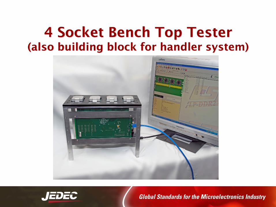
4 Socket Bench Top Tester (also building block for handler system)

Production Automated Test(128 sockets simultaneously)

Production Burn-in Test

Any Questions?

Thank You !