precision, 20 mhz, cmos, rail-to-rail input/output ...€¦ · precision, 20 mhz, cmos,...
TRANSCRIPT

Precision, 20 MHz, CMOS, Rail-to-Rail Input/Output Operational Amplifiers
Data Sheet AD8615/AD8616/AD8618
Rev. G Document Feedback Information furnished by Analog Devices is believed to be accurate and reliable. However, no responsibility is assumed by Analog Devices for its use, nor for any infringements of patents or other rights of third parties that may result from its use. Specifications subject to change without notice. No license is granted by implication or otherwise under any patent or patent rights of Analog Devices. Trademarks and registered trademarks are the property of their respective owners.
One Technology Way, P.O. Box 9106, Norwood, MA 02062-9106, U.S.A.Tel: 781.329.4700 ©2004–2014 Analog Devices, Inc. All rights reserved. Technical Support www.analog.com
FEATURES Low offset voltage: 65 μV maximum Single-supply operation: 2.7 V to 5.0 V Low noise: 8 nV/√Hz Wide bandwidth: >20 MHz Slew rate: 12 V/μs High output current: 150 mA No phase reversal Low input bias current: 1 pA Low supply current: 2 mA Unity-gain stable
APPLICATIONS Barcode scanners Battery-powered instrumentation Multipole filters Sensors ASIC input or output amplifiers Audio Photodiode amplification
GENERAL DESCRIPTION The AD8615/AD8616/AD8618 are single/dual/quad, rail-to-rail, input and output, single-supply amplifiers featuring very low offset voltage, wide signal bandwidth, and low input voltage and current noise. The parts use a patented trimming technique that achieves superior precision without laser trimming. The AD8615/AD8616/AD8618 are fully specified to operate from 2.7 V to 5 V single supplies.
The combination of >20 MHz bandwidth, low offset, low noise, and low input bias current makes these amplifiers useful in a wide variety of applications. Filters, integrators, photodiode amplifiers, and high impedance sensors all benefit from the combination of performance features. AC applications benefit from the wide bandwidth and low distortion. The AD8615/AD8616/ AD8618 offer the highest output drive capability of the DigiTrim® family, which is excellent for audio line drivers and other low impedance applications.
Applications for the parts include portable and low powered instrumentation, audio amplification for portable devices, portable phone headsets, bar code scanners, and multipole filters. The ability to swing rail-to-rail at both the input and output enables designers to buffer CMOS ADCs, DACs, ASICs, and other wide output swing devices in single-supply systems.
PIN CONFIGURATIONS
AD8615
TOP VIEW(Not to Scale)
OUT 1
V– 2
+IN 3
V+
–IN
5
4
0464
8-00
1
Figure 1. 5-Lead TSOT-23 (UJ-5)
OUT A 1
–IN A 2
+IN A 3
V– 4
V+8
OUT B7
–IN B6
+IN B5
AD8616TOP VIEW
(Not to Scale)
0464
8-00
2
Figure 2. 8-Lead MSOP (RM-8)
OUT A 1
–IN A 2
+IN A 3
V– 4
V+8
OUT B7
–IN B6
+IN B5
AD8616TOP VIEW
(Not to Scale)
0464
8-00
3
Figure 3. 8-Lead SOIC (R-8)
AD8618TOP VIEW
(Not to Scale)
OUT A OUT D–IN A –IN D+IN A +IN D
V+ V–+IN B +IN C–IN B –IN C
14
8
1
7OUT B OUT C
0464
8-00
4
Figure 4. 14-Lead TSSOP (RU-14)
AD8618TOP VIEW
(Not to Scale)
OUT A 1 OUT D14
–IN A 2 –IN D13
+IN A 3 +IN D12
V+ 4 V–11
+IN B 5 +IN C10
–IN B 6 –IN C9
OUT B 7 OUT C8
0464
8-00
5
Figure 5. 14-Lead SOIC (R-14)
The AD8615/AD8616/AD8618 are specified over the extended industrial temperature range (−40°C to +125°C). The AD8615 is available in 5-lead TSOT-23 package. The AD8616 is available in 8-lead MSOP and narrow SOIC surface-mount packages; the MSOP version is available in tape and reel only. The AD8618 is available in 14-lead SOIC and TSSOP packages.

AD8615/AD8616/AD8618 Data Sheet
TABLE OF CONTENTS Features .............................................................................................. 1 Applications ....................................................................................... 1 General Description ......................................................................... 1 Pin Configurations ........................................................................... 1 Revision History ............................................................................... 2 Specifications ..................................................................................... 3 Absolute Maximum Ratings ............................................................ 5
Thermal Resistance ...................................................................... 5 ESD Caution .................................................................................. 5
Typical Performance Characteristics ............................................. 6 Applications Information .............................................................. 11
Input Overvoltage Protection ................................................... 11
Output Phase Reversal ............................................................... 11 Driving Capacitive Loads .......................................................... 11 Overload Recovery Time .......................................................... 12 D/A Conversion ......................................................................... 12 Low Noise Applications ............................................................. 12 High Speed Photodiode Preamplifier ...................................... 13 Active Filters ............................................................................... 13 Power Dissipation....................................................................... 13 Power Calculations for Varying or Unknown Loads ............. 14
Outline Dimensions ....................................................................... 15 Ordering Guide .......................................................................... 17
REVISION HISTORY 6/14—Rev. F to Rev. G Changes to Input Overvoltage Protection Section ..................... 11 3/14—Rev. E to Rev. F Changes to Differential Input Voltage Parameter, Table 3 .......... 5 Updated Outline Dimensions ....................................................... 15 Changes to Ordering Guide .......................................................... 17 9/08—Rev. D to Rev. E Changes to General Description Section ...................................... 1 Updated Outline Dimensions ....................................................... 15 Changes to Ordering Guide .......................................................... 17 5/08—Rev. C to Rev. D Changes to Layout ............................................................................ 1 Changes to Figure 38 ...................................................................... 11 Changes to Figure 44 and Figure 45 ............................................. 13 Changes to Layout .......................................................................... 15 Changes to Layout .......................................................................... 16
6/05—Rev. B to Rev. C Change to Table 1 .............................................................................. 3 Change to Table 2 .............................................................................. 4 Change to Figure 20 .......................................................................... 8 1/05—Rev. A to Rev. B Added AD8615 ................................................................... Universal Changes to Figure 12 ......................................................................... 8 Deleted Figure 19; Renumbered Subsequently .............................. 8 Changes to Figure 20 ......................................................................... 9 Changes to Figure 29 ...................................................................... 10 Changes to Figure 31 ...................................................................... 11 Deleted Figure 34; Renumbered Subsequently ........................... 11 Deleted Figure 35; Renumbered Subsequently ........................... 35 4/04—Rev. 0 to Rev. A Added AD8618 ................................................................... Universal Updated Outline Dimensions ....................................................... 16 1/04—Revision 0: Initial Version
Rev. G | Page 2 of 20
Data Sheet AD8615/AD8616/AD8618
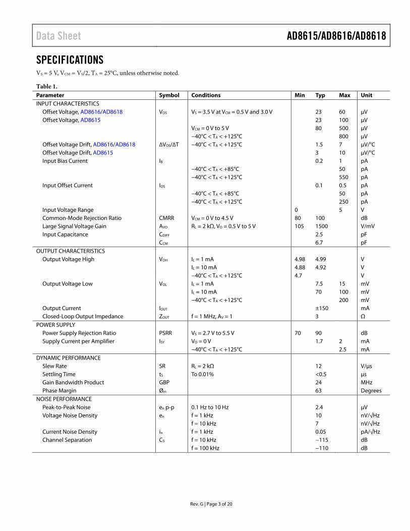
SPECIFICATIONS VS = 5 V, VCM = VS/2, TA = 25°C, unless otherwise noted.
Table 1. Parameter Symbol Conditions Min Typ Max Unit INPUT CHARACTERISTICS
Offset Voltage, AD8616/AD8618 VOS VS = 3.5 V at VCM = 0.5 V and 3.0 V 23 60 µV Offset Voltage, AD8615 23 100 µV VCM = 0 V to 5 V 80 500 µV −40°C < TA < +125°C 800 µV Offset Voltage Drift, AD8616/AD8618 ∆VOS/∆T −40°C < TA < +125°C 1.5 7 µV/°C Offset Voltage Drift, AD8615 3 10 µV/°C Input Bias Current IB 0.2 1 pA
−40°C < TA < +85°C 50 pA −40°C < TA < +125°C 550 pA
Input Offset Current IOS 0.1 0.5 pA −40°C < TA < +85°C 50 pA −40°C < TA < +125°C 250 pA
Input Voltage Range 0 5 V Common-Mode Rejection Ratio CMRR VCM = 0 V to 4.5 V 80 100 dB Large Signal Voltage Gain AVO RL = 2 kΩ, VO = 0.5 V to 5 V 105 1500 V/mV Input Capacitance CDIFF 2.5 pF
CCM 6.7 pF OUTPUT CHARACTERISTICS
Output Voltage High VOH IL = 1 mA 4.98 4.99 V IL = 10 mA 4.88 4.92 V
−40°C < TA < +125°C 4.7 V Output Voltage Low VOL IL = 1 mA 7.5 15 mV
IL = 10 mA 70 100 mV −40°C < TA < +125°C 200 mV
Output Current IOUT ±150 mA Closed-Loop Output Impedance ZOUT f = 1 MHz, AV = 1 3 Ω
POWER SUPPLY Power Supply Rejection Ratio PSRR VS = 2.7 V to 5.5 V 70 90 dB Supply Current per Amplifier ISY VO = 0 V 1.7 2 mA −40°C < TA < +125°C 2.5 mA
DYNAMIC PERFORMANCE Slew Rate SR RL = 2 kΩ 12 V/µs Settling Time tS To 0.01% <0.5 µs Gain Bandwidth Product GBP 24 MHz Phase Margin Øm 63 Degrees
NOISE PERFORMANCE Peak-to-Peak Noise en p-p 0.1 Hz to 10 Hz 2.4 µV Voltage Noise Density en f = 1 kHz 10 nV/√Hz
f = 10 kHz 7 nV/√Hz Current Noise Density in f = 1 kHz 0.05 pA/√Hz Channel Separation CS f = 10 kHz −115 dB
f = 100 kHz −110 dB
Rev. G | Page 3 of 20

AD8615/AD8616/AD8618 Data Sheet VS = 2.7 V, VCM = VS/2, TA = 25°C, unless otherwise noted.
Table 2. Parameter Symbol Conditions Min Typ Max Unit INPUT CHARACTERISTICS
Offset Voltage, AD8616/AD8618 VOS VS = 3.5 V at VCM = 0.5 V and 3.0 V 23 65 µV Offset Voltage, AD8615 23 100 µV VCM = 0 V to 2.7 V 80 500 µV −40°C < TA < +125°C 800 µV
Offset Voltage Drift, AD8616/AD8618 ∆VOS/∆T −40°C < TA < +125°C 1.5 7 µV/°C Offset Voltage Drift, AD8615 3 10 µV/°C Input Bias Current IB 0.2 1 pA
−40°C < TA < +85°C 50 pA −40°C < TA < +125°C 550 pA
Input Offset Current IOS 0.1 0.5 pA −40°C < TA < +85°C 50 pA −40°C < TA < +125°C 250 pA
Input Voltage Range 0 2.7 V Common-Mode Rejection Ratio CMRR VCM = 0 V to 2.7 V 80 100 dB Large Signal Voltage Gain AVO RL = 2 kΩ, VO = 0.5 V to 2.2 V 55 150 V/mV Input Capacitance CDIFF 2.5 pF
CCM 7.8 pF OUTPUT CHARACTERISTICS
Output Voltage High VOH IL = 1 mA 2.65 2.68 V −40°C < TA < +125°C 2.6 V
Output Voltage Low VOL IL = 1 mA 11 25 mV −40°C < TA < +125°C 30 mV
Output Current IOUT ±50 mA Closed-Loop Output Impedance ZOUT f = 1 MHz, AV = 1 3 Ω
POWER SUPPLY Power Supply Rejection Ratio PSRR VS = 2.7 V to 5.5 V 70 90 dB Supply Current per Amplifier ISY VO = 0 V 1.7 2 mA
−40°C < TA < +125°C 2.5 mA DYNAMIC PERFORMANCE
Slew Rate SR RL = 2 kΩ 12 V/µs Settling Time tS To 0.01% <0.3 µs Gain Bandwidth Product GBP 23 MHz Phase Margin Øm 42 Degrees
NOISE PERFORMANCE Peak-to-Peak Noise en p-p 0.1 Hz to 10 Hz 2.1 µV Voltage Noise Density en f = 1 kHz 10 nV/√Hz f = 10 kHz 7 nV/√Hz Current Noise Density in f = 1 kHz 0.05 pA/√Hz Channel Separation CS f = 10 kHz −115 dB
f = 100 kHz −110 dB
Rev. G | Page 4 of 20
Data Sheet AD8615/AD8616/AD8618
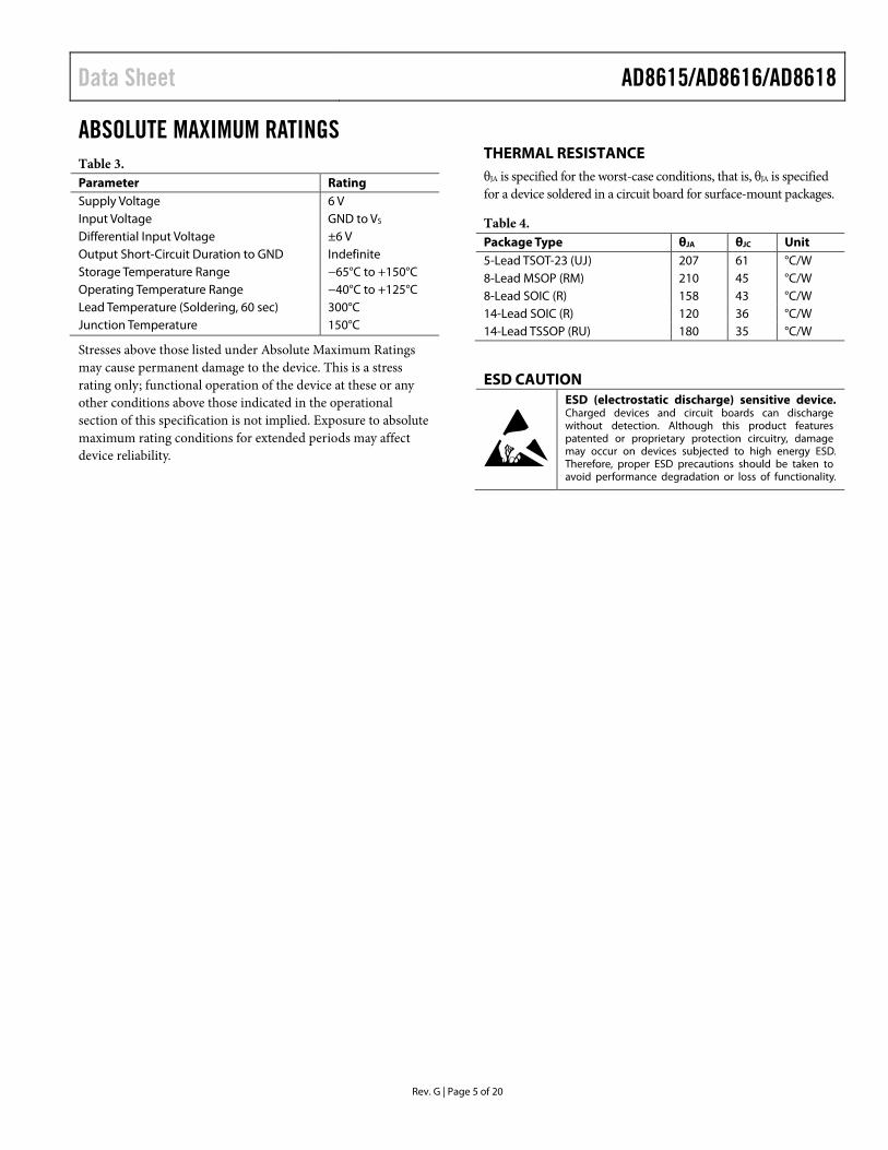
ABSOLUTE MAXIMUM RATINGS Table 3. Parameter Rating Supply Voltage 6 V Input Voltage GND to VS Differential Input Voltage ±6 V Output Short-Circuit Duration to GND Indefinite Storage Temperature Range −65°C to +150°C Operating Temperature Range −40°C to +125°C Lead Temperature (Soldering, 60 sec) 300°C Junction Temperature 150°C
Stresses above those listed under Absolute Maximum Ratings may cause permanent damage to the device. This is a stress rating only; functional operation of the device at these or any other conditions above those indicated in the operational section of this specification is not implied. Exposure to absolute maximum rating conditions for extended periods may affect device reliability.
THERMAL RESISTANCE θJA is specified for the worst-case conditions, that is, θJA is specified for a device soldered in a circuit board for surface-mount packages.
Table 4. Package Type θJA θJC Unit 5-Lead TSOT-23 (UJ) 207 61 °C/W 8-Lead MSOP (RM) 210 45 °C/W 8-Lead SOIC (R) 158 43 °C/W 14-Lead SOIC (R) 120 36 °C/W 14-Lead TSSOP (RU) 180 35 °C/W
ESD CAUTION
Rev. G | Page 5 of 20

AD8615/AD8616/AD8618 Data Sheet
TYPICAL PERFORMANCE CHARACTERISTICS
0
200
600
1400
1800
2200
1000
400
1200
1600
2000
800
NU
MB
ER O
FA
MPL
IFIE
RS
–700 –500 –300 –100 100 300 500 700
OFFSET VOLTAGE (µV)
VS = 5VTA = 25°CVCM = 0V TO 5V
0464
8-00
6
Figure 6. Input Offset Voltage Distribution
0
2
6
14
18
22
10
4
12
16
20
8
NU
MB
ER O
FA
MPL
IFIE
RS
0 2 4 6 8 10 12
TCVOS (µV/°C)
VS = ±2.5VTA = –40°C TO +125°CVCM = 0V
0464
8-00
7
Figure 7. Offset Voltage Drift Distribution
–400
–500
–300
–200
–100
0
100
200
300
400
500
INPU
T O
FFSE
T VO
LTA
GE
(µV)
0 0.5 1.0 1.5 2.0 2.5 3.0 3.5 4.0 4.5 5.0
COMMON-MODE VOLTAGE (V)
VS = 5VTA = 25°C
0464
8-00
8
Figure 8. Input Offset Voltage vs. Common-Mode Voltage
(200 Units, Five Wafer Lots Including Process Skews)
0
50
100
150
200
250
300
350
INPU
T B
IAS
CU
RR
ENT
(pA
)
0 25 50 75 100 125
TEMPERATURE (-°C)
VS = ±2.5V
0464
8-00
9
Figure 9. Input Bias Current vs. Temperature
SINKSOURCE
1000
100
10
1
0.10.001 0.01 0.1 1 10
ILOAD (mA)
V SY
– V O
UT
(mV)
100
VS = 5VTA = 25°C
0464
8-01
0
Figure 10. Output Voltage to Supply Rail vs. Load Current
0
20
40
60
80
100
120
OU
TPU
TSA
TUR
ATIO
NVO
LTA
GE
(mV)
–40 –25 –10 5 20 35 50 65 80 95 110 125
TEMPERATURE (°C)
VS = 5V
1mA LOAD
10mA LOAD04
648-
011
Figure 11. Output Saturation Voltage vs. Temperature
Rev. G | Page 6 of 20

Data Sheet AD8615/AD8616/AD8618
1M 10M
100
80
60
40
20
0
–20
–40
–60
–80
–100
GA
IN (d
B)
225
180
135
90
45
0
–45
–90
–135
–180
–225
PHA
SE (D
egre
es)
VS = ±2.5VTA = 25°CØm = 63°
60MFREQUENCY (Hz) 04
648-
012
Figure 12. Open-Loop Gain and Phase vs. Frequency
0
0.5
1.0
1.5
2.0
2.5
3.0
3.5
4.0
4.5
5.0
OU
TPU
TSW
ING
(Vp-
p)
FREQUENCY (Hz)
10k1k 100k 1M 10M
VS = 5.0VVIN = 4.9V p-pTA = 25°CRL = 2kΩAV = 1
0464
8-01
3
Figure 13. Closed-Loop Output Voltage Swing vs. Frequency
0
10
20
30
40
50
60
70
80
90
100
OU
TPU
T IM
PED
AN
CE
(Ω)
1k 10k 100k 1M 10M 100M
FREQUENCY (Hz)
AV = 100 AV = 1
AV = 10
VS = ±2.5V
0464
8-01
4
Figure 14. Output Impedance vs. Frequency
0
20
40
60
80
100
120
CM
RR
(dB
)
FREQUENCY (Hz)
10k1k 100k 1M 10M
VS = ±2.5V
0464
8-01
5
Figure 15. CMRR vs. Frequency
0
20
40
60
80
100
120
PSR
R (d
B)
FREQUENCY (Hz)
10k1k 100k 1M 10M
VS = ±2.5V
0464
8-01
6
Figure 16. PSRR vs. Frequency
5
0
10
15
20
25
30
35
40
45
50
SMA
LL-S
IGN
AL O
VER
SHO
OT
(%)
CAPACITANCE (pF)
10 100 1000
VS = 5VRL = ∞TA = 25°CAV = 1
+OS
–OS
0464
8-01
7
Figure 17. Small-Signal Overshoot vs. Load Capacitance
Rev. G | Page 7 of 20

AD8615/AD8616/AD8618 Data Sheet
0
0.4
0.8
0.6
0.2
1.2
1.0
SUPP
LYC
UR
REN
TPE
RA
MPL
IFIE
R(m
A)
1.6
1.4
2.0
1.8
2.4
2.2
–40 –25 –10 5 20 35 50 65 80 95 110 125
TEMPERATURE (°C)
VS = 2.7V
VS = 5V
0464
8-01
8
Figure 18. Supply Current vs. Temperature
200
0
400
600
800
1000
1200
1400
1600
1800
2000
SUPP
LY C
UR
REN
T PE
RA
MPL
IFIE
R (µ
A)
0 0.5 1.0 1.5 2.0 2.5 3.0 3.5 4.0 4.5 5.0
SUPPLY VOLTAGE (V) 0464
8-01
9
Figure 19. Supply Current per Amplifier vs. Supply Voltage
1k
100
10
110 100 1k 10k 100k
FREQUENCY (Hz)
VOLT
AG
E N
OIS
E D
ENSI
TY (n
V/ H
z0.5
)
VS = ±2.5VVS = ±1.35V
0464
8-02
0
Figure 20. Voltage Noise Density vs. Frequency
VOLT
AG
E(5
0mV/
DIV
)
TIME (1µs/DIV)
VS = 5VRL = 10kΩCL = 200pFAV = 1
0464
8-02
1
Figure 21. Small Signal Transient Response
VOLT
AG
E (5
00m
V/D
IV)
TIME (1s/DIV)
VS = 5VRL = 10kΩCL = 200pFAV = 1
0464
8-02
2
Figure 22. Large Signal Transient Response
THD
+N (%
)
0.0001
0.01
0.001
0.1
FREQUENCY (Hz)
20 100 1k 20k
VS = ±2.5VVIN = 0.5V rmsAV = 1BW = 22kHzRL = 100kΩ
0464
8-02
3
Figure 23. THD + N vs. Frequency
Rev. G | Page 8 of 20
Data Sheet AD8615/AD8616/AD8618
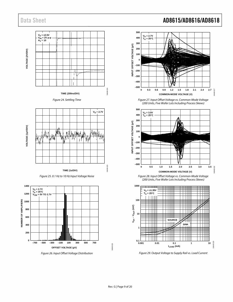
Rev. G | Page 9 of 20
VOLT
AG
E(2
V/D
IV)
VS = ±2.5VVIN = 2V p-pAV = 10
TIME (200ns/DIV) 0464
8-02
4
Figure 24. Settling Time
VOLT
AG
E(1
µV/D
IV)
TIME (1s/DIV)
VS = 2.7V
0464
8-02
5
Figure 25. 0.1 Hz to 10 Hz Input Voltage Noise
0
200
400
600
800
1000
1200
1400
NU
MB
ER O
FA
MPL
IFIE
RS
–700 –500 –300 –100 100 300 500 700
OFFSET VOLTAGE (µV)
VS = 2.7VTA = 25°CVCM = 0V TO 2.7V
0464
8-02
6
Figure 26. Input Offset Voltage Distribution
–400
–500
–300
–200
–100
0
100
200
300
400
500
INPU
T O
FFSE
T VO
LTA
GE
(µV)
0 0.3 0.6 0.9 1.2 1.5 1.8 2.1 2.4 2.7
COMMON-MODE VOLTAGE (V)
VS = 2.7VTA = 25°C
0464
8-02
7
Figure 27. Input Offset Voltage vs. Common-Mode Voltage (200 Units, Five Wafer Lots Including Process Skews)
–400
–500
–300
–200
–100
0
100
200
300
400
500
INPU
T O
FFSE
T VO
LTA
GE
(µV)
0 0.5 1.0 1.5 2.0 2.5 3.0 3.5
COMMON-MODE VOLTAGE (V)
VS = 3.5VTA = 25°C
0464
8-02
8
Figure 28. Input Offset Voltage vs. Common-Mode Voltage (200 Units, Five Wafer Lots Including Process Skews)
SINK
SOURCE
1000
100
10
1
0.10.001 0.01 0.1 1 10
ILOAD (mA)
V SY
– V O
UT (m
V)
VS = ±1.35VTA = 25°C
0464
8-02
9
Figure 29. Output Voltage to Supply Rail vs. Load Current

AD8615/AD8616/AD8618 Data Sheet
Rev. G | Page 10 of 20
0
2
4
6
8
10
12
14
16
18
OU
TP
UT
SA
TU
RA
TIO
NV
OLT
AG
E(m
V)
–40 –25 –10 5 20 35 50 65 80 95 110 125
TEMPERATURE (°C)
VS = 2.7V
VOH @ 1mA LOAD
VOL @ 1mA LOAD
0464
8-03
0Figure 30. Output Saturation Voltage vs. Temperature
1M 10M
100
80
60
40
20
0
–20
–40
–60
–80
–100
GA
IN (
dB
)
225
180
135
90
45
0
–45
–90
–135
–180
–225
PH
AS
E (
Deg
rees
)
VS = ±1.35VTA = 25°CØm = 42°
60MFREQUENCY (Hz) 04
648-
031
Figure 31. Open-Loop Gain and Phase vs. Frequency
0
0.3
0.6
0.9
1.2
1.5
1.8
2.1
2.4
2.7
OU
TP
UT
SW
ING
(Vp
-p)
FREQUENCY (Hz)
10k1k 100k 1M 10M
VS = 2.7VVIN = 2.6V p-pTA = 25°CRL = 2kΩAV = 1
0464
8-03
2
Figure 32. Closed-Loop Output Voltage Swing vs. Frequency
5
0
10
15
20
25
30
35
40
45
50
SM
AL
L S
IGN
AL
OV
ER
SH
OO
T (
%)
CAPACITANCE (pF)
10 100 1000
VS = ±1.35VRL = ∞TA = 25°CAV = 1
+OS–OS
0464
8-03
3
Figure 33. Small Signal Overshoot vs. Load Capacitance
VO
LTA
GE
(50m
V/D
IV)
TIME (1µs/DIV)
VS = 2.7VRL = 10kΩCL = 200pFAV = 1
0464
8-03
4
Figure 34. Small Signal Transient Response
VO
LT
AG
E (
500m
V/D
IV)
TIME (1µs/DIV)
VS = 2.7VRL = 10kΩCL = 200pFAV = 1
0464
8-03
5
Figure 35. Large Signal Transient Response

Data Sheet AD8615/AD8616/AD8618
Rev. G | Page 11 of 20
APPLICATIONS INFORMATION INPUT OVERVOLTAGE PROTECTION If the voltage applied at either input exceeds the supplies, place external resistors in series with the inputs. The resistor values can be determined by the equation
mA5VSY
S
IN
RV
The extremely low input bias current allows the use of larger resistors, which allows the user to apply higher voltages at the inputs. The use of these resistors adds thermal noise, which contributes to the overall output voltage noise of the amplifier.
For example, a 10 kΩ resistor has less than 13 nV/√Hz of thermal noise and less than 10 nV of error voltage at room temperature.
OUTPUT PHASE REVERSAL The AD8615/AD8616/AD8618 are immune to phase inversion, a phenomenon that occurs when the voltage applied at the input of the amplifier exceeds the maximum input common mode.
Phase reversal can cause permanent damage to the amplifier and can create lock ups in systems with feedback loops.
VO
LTA
GE
(2V
/DIV
)
TIME (2ms/DIV)
VINVOUT
VS = ±2.5VVIN = 6V p-pAV = 1RL = 10kΩ
0464
8-03
6
Figure 36. No Phase Reversal
DRIVING CAPACITIVE LOADS Although the AD8615/AD8616/AD8618 are capable of driving capacitive loads of up to 500 pF without oscillating, a large amount of overshoot is present when operating at frequencies above 100 kHz. This is especially true when the amplifier is configured in positive unity gain (worst case). When such large capacitive loads are required, the use of external compensation is highly recommended.
This reduces the overshoot and minimizes ringing, which in turn improves the frequency response of the AD8615/AD8616/ AD8618. One simple technique for compensation is the snubber, which consists of a simple RC network. With this circuit in place, output swing is maintained and the amplifier is stable at all gains.
Figure 38 shows the implementation of the snubber, which reduces overshoot by more than 30% and eliminates ringing that can cause instability. Using the snubber does not recover the loss of bandwidth incurred from a heavy capacitive load.
VO
LT
AG
E (
100m
V/D
IV)
TIME (2µs/DIV)
VS = ±2.5VAV = 1CL = 500pF
0464
8-03
7
Figure 37. Driving Heavy Capacitive Loads Without Compensation
V+200Ω
500pF500pF
V–
VEE
VCC200mV–
+
–
0464
8-03
8
Figure 38. Snubber Network
VO
LT
AG
E (
100m
V/D
IV)
TIME (10µs/DIV)
VS = ±2.5VAV = 1RS = 200ΩCS = 500pFCL = 500pF
0464
8-03
9
Figure 39. Driving Heavy Capacitive Loads Using the Snubber Network

AD8615/AD8616/AD8618 Data Sheet
Rev. G | Page 12 of 20
OVERLOAD RECOVERY TIME Overload recovery time is the time it takes the output of the amplifier to come out of saturation and recover to its linear region. Overload recovery is particularly important in applications where small signals must be amplified in the presence of large transients. Figure 40 and Figure 41 show the positive and negative overload recovery times of the AD8616. In both cases, the time elapsed before the AD8616 comes out of saturation is less than 1 μs. In addition, the symmetry between the positive and negative recovery times allows excellent signal rectification without distortion to the output signal.
TIME (1µs/DIV)
VS = ±2.5VRL = 10kΩAV = 100VIN = 50mV
–50mV
+2.5V
0V
0V
0464
8-04
0
Figure 40. Positive Overload Recovery
TIME (1µs/DIV)
VS = ±2.5VRL = 10kΩAV = 100VIN = 50mV
+50mV
–2.5V
0V
0V
0464
8-04
1
Figure 41. Negative Overload Recovery
D/A CONVERSION The AD8616 can be used at the output of high resolution DACs. The low offset voltage, fast slew rate, and fast settling time make the part suitable to buffer voltage output or current output DACs.
Figure 42 shows an example of the AD8616 at the output of the AD5542. The AD8616’s rail-to-rail output and low distortion help maintain the accuracy needed in data acquisition systems and automated test equipment.
AD5542 VOUT
UNIPOLAROUTPUT
AGNDDGND
REFS 1/2AD8616
REFFVDDSERIAL
INTERFACE
0.1µF 0.1µF
10µF5V 2.5V
+
CS
DIN
SCLK
LDAC
0464
8-04
2
Figure 42. Buffering DAC Output
LOW NOISE APPLICATIONS Although the AD8618 typically has less than 8 nV/√Hz of voltage noise density at 1 kHz, it is possible to reduce it further. A simple method is to connect the amplifiers in parallel, as shown in Figure 43. The total noise at the output is divided by the square root of the number of amplifiers. In this case, the total noise is approximately 4 nV/√Hz at room temperature. The 100 Ω resistor limits the current and provides an effective output resistance of 50 Ω.
V–
R3
100ΩR1
10Ω
V+VIN
3
2
1
R2
1kΩ
V–
R6
100ΩR4
10Ω
V+
3
2
1
R5
1kΩ
V–
R9
100ΩR7
10Ω
V+
3
2
1
R8
1kΩ
V–
R12
100ΩR10
10Ω
V+
3
2
1
R11
1kΩ
VOUT
0464
8-04
3
Figure 43. Noise Reduction
Data Sheet AD8615/AD8616/AD8618
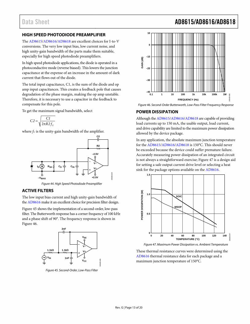
HIGH SPEED PHOTODIODE PREAMPLIFIER The AD8615/AD8616/AD8618 are excellent choices for I-to-V conversions. The very low input bias, low current noise, and high unity-gain bandwidth of the parts make them suitable, especially for high speed photodiode preamplifiers.
In high speed photodiode applications, the diode is operated in a photoconductive mode (reverse biased). This lowers the junction capacitance at the expense of an increase in the amount of dark current that flows out of the diode.
The total input capacitance, C1, is the sum of the diode and op amp input capacitances. This creates a feedback pole that causes degradation of the phase margin, making the op amp unstable. Therefore, it is necessary to use a capacitor in the feedback to compensate for this pole.
To get the maximum signal bandwidth, select
Uf2R1C2C
π=
2
where fU is the unity-gain bandwidth of the amplifier.
V–
+2.5V
V+
–2.5V
R2
C2
CINCDRSHID
–VBIAS
–
+
0464
8-04
4
Figure 44. High Speed Photodiode Preamplifier
ACTIVE FILTERS The low input bias current and high unity-gain bandwidth of the AD8616 make it an excellent choice for precision filter design.
Figure 45 shows the implementation of a second-order, low-pass filter. The Butterworth response has a corner frequency of 100 kHz and a phase shift of 90°. The frequency response is shown in Figure 46.
V–
VCC
V+
VEE
2nF
1nF
1.1kΩ1.1kΩ
VIN
0464
8-04
5
Figure 45. Second-Order, Low-Pass Filter
–40
–30
–20
–10
0
10
GA
IN (d
B)
10.1 10 100 1k 10k 100k 1M
FREQUENCY (Hz) 0464
8-04
6
Figure 46. Second-Order Butterworth, Low-Pass Filter Frequency Response
POWER DISSIPATION Although the AD8615/AD8616/AD8618 are capable of providing load currents up to 150 mA, the usable output, load current, and drive capability are limited to the maximum power dissipation allowed by the device package.
In any application, the absolute maximum junction temperature for the AD8615/AD8616/AD8618 is 150°C. This should never be exceeded because the device could suffer premature failure. Accurately measuring power dissipation of an integrated circuit is not always a straightforward exercise; Figure 47 is a design aid for setting a safe output current drive level or selecting a heat sink for the package options available on the AD8616.
POW
ER D
ISSI
PATI
ON
(W)
TEMPERATURE (°C)0
0
0.5
1.0
1.5
20 40 60 80 120100 140
SOIC
MSOP
0464
8-04
7
Figure 47. Maximum Power Dissipation vs. Ambient Temperature
These thermal resistance curves were determined using the AD8616 thermal resistance data for each package and a maximum junction temperature of 150°C.
Rev. G | Page 13 of 20

AD8615/AD8616/AD8618 Data Sheet The following formula can be used to calculate the internal junction temperature of the AD8615/AD8616/AD8618 for any application:
TJ = PDISS × θJA + TA
where: TJ = junction temperature PDISS = power dissipation θJA = package thermal resistance, junction-to-case TA = ambient temperature of the circuit
To calculate the power dissipated by the AD8615/AD8616/ AD8618, use the following:
PDISS = ILOAD × (VS – VOUT)
where: ILOAD = output load current VS = supply voltage VOUT = output voltage
The quantity within the parentheses is the maximum voltage developed across either output transistor.
POWER CALCULATIONS FOR VARYING OR UNKNOWN LOADS Often, calculating power dissipated by an integrated circuit to determine if the device is being operated in a safe range is not as simple as it may seem. In many cases, power cannot be directly measured. This may be the result of irregular output waveforms or varying loads. Indirect methods of measuring power are required.
There are two methods to calculate power dissipated by an integrated circuit. The first is to measure the package temperature and the board temperature. The second is to directly measure the circuit’s supply current.
Calculating Power by Measuring Ambient Temperature and Case Temperature
The two equations for calculating the junction temperature are
TJ = TA + P θJA
where: TJ = junction temperature TA = ambient temperature θJA = the junction-to-ambient thermal resistance
TJ = TC + P θJC
where: TC is case temperature. θJA and θJC are given in the data sheet.
The two equations for calculating P (power) are
TA + P θJA = TC + P θJC
P = (TA − TC)/(θJC − θJA)
Once the power is determined, it is necessary to recalculate the junction temperature to ensure that the temperature was not exceeded.
The temperature should be measured directly on and near the package but not touching it. Measuring the package can be difficult. A very small bimetallic junction glued to the package can be used, or an infrared sensing device can be used, if the spot size is small enough.
Calculating Power by Measuring Supply Current
If the supply voltage and current are known, power can be calculated directly. However, the supply current can have a dc component with a pulse directed into a capacitive load, which can make the rms current very difficult to calculate. This difficulty can be overcome by lifting the supply pin and inserting an rms current meter into the circuit. For this method to work, make sure the current is delivered by the supply pin being measured. This is usually a good method in a single-supply system; however, if the system uses dual supplies, both supplies may need to be monitored.
Rev. G | Page 14 of 20

Data Sheet AD8615/AD8616/AD8618
OUTLINE DIMENSIONS
0915
08-A
*COMPLIANT TO JEDEC STANDARDS MO-193-AB WITHTHE EXCEPTION OF PACKAGE HEIGHT AND THICKNESS.
1.60 BSC 2.80 BSC
1.90BSC
0.95 BSC
0.200.08
0.600.450.30
8°4°0°
0.500.30
0.10 MAX
*1.00 MAX
*0.90 MAX0.70 NOM
2.90 BSC
5 4
1 2 3
SEATINGPLANE
Figure 48. 5-Lead Thin Small Outline Transistor Package [TSOT]
(UJ-5) Dimensions shown in millimeters
COMPLIANT TO JEDEC STANDARDS MO-187-AA
6°0°
0.800.550.40
4
8
1
5
0.65 BSC
0.400.25
1.10 MAX
3.203.002.80
COPLANARITY0.10
0.230.09
3.203.002.80
5.154.904.65
PIN 1IDENTIFIER
15° MAX0.950.850.75
0.150.05
10-0
7-20
09-B
Figure 49. 8-Lead Mini Small Outline Package [MSOP]
(RM-8) Dimensions shown in millimeters
Rev. G | Page 15 of 20
AD8615/AD8616/AD8618 Data Sheet
CONTROLLING DIMENSIONS ARE IN MILLIMETERS; INCH DIMENSIONS(IN PARENTHESES) ARE ROUNDED-OFF MILLIMETER EQUIVALENTS FORREFERENCE ONLY AND ARE NOT APPROPRIATE FOR USE IN DESIGN.
COMPLIANT TO JEDEC STANDARDS MS-012-AA
0124
07-A
0.25 (0.0098)0.17 (0.0067)
1.27 (0.0500)0.40 (0.0157)
0.50 (0.0196)0.25 (0.0099) 45°
8°0°
1.75 (0.0688)1.35 (0.0532)
SEATINGPLANE
0.25 (0.0098)0.10 (0.0040)
41
8 5
5.00 (0.1968)4.80 (0.1890)
4.00 (0.1574)3.80 (0.1497)
1.27 (0.0500)BSC
6.20 (0.2441)5.80 (0.2284)
0.51 (0.0201)0.31 (0.0122)
COPLANARITY0.10
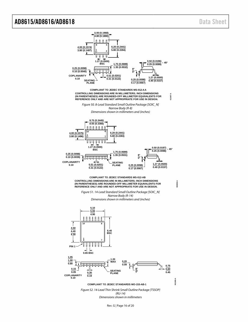
Figure 50. 8-Lead Standard Small Outline Package [SOIC_N]
Narrow Body (R-8) Dimensions shown in millimeters and (inches)
CONTROLLING DIMENSIONS ARE IN MILLIMETERS; INCH DIMENSIONS(IN PARENTHESES) ARE ROUNDED-OFF MILLIMETER EQUIVALENTS FORREFERENCE ONLY AND ARE NOT APPROPRIATE FOR USE IN DESIGN.
COMPLIANT TO JEDEC STANDARDS MS-012-AB06
0606
-A
14 8
71
6.20 (0.2441)5.80 (0.2283)
4.00 (0.1575)3.80 (0.1496)
8.75 (0.3445)8.55 (0.3366)
1.27 (0.0500)BSC
SEATINGPLANE
0.25 (0.0098)0.10 (0.0039)
0.51 (0.0201)0.31 (0.0122)
1.75 (0.0689)1.35 (0.0531)
0.50 (0.0197)0.25 (0.0098)
1.27 (0.0500)0.40 (0.0157)
0.25 (0.0098)0.17 (0.0067)
COPLANARITY0.10
8°0°
45°
Figure 51. 14-Lead Standard Small Outline Package [SOIC_N]
Narrow Body (R-14) Dimensions shown in millimeters and (inches)
COMPLIANT TO JEDEC STANDARDS MO-153-AB-1 0619
08-A
8°0°
4.504.404.30
14 8
71
6.40BSC
PIN 1
5.105.004.90
0.65 BSC
0.150.05 0.30
0.19
1.20MAX
1.051.000.80
0.200.09 0.75
0.600.45
COPLANARITY0.10
SEATINGPLANE
Figure 52. 14-Lead Thin Shrink Small Outline Package [TSSOP]
(RU-14) Dimensions shown in millimeters
Rev. G | Page 16 of 20

Data Sheet AD8615/AD8616/AD8618
ORDERING GUIDE Model1 Temperature Range Package Description Package Option Branding AD8615AUJZ-R2 –40°C to +125°C 5-Lead TSOT-23 UJ-5 BKA AD8615AUJZ-REEL –40°C to +125°C 5-Lead TSOT-23 UJ-5 BKA AD8615AUJZ-REEL7 –40°C to +125°C 5-Lead TSOT-23 UJ-5 BKA AD8616ARMZ –40°C to +125°C 8-Lead MSOP RM-8 A0K AD8616ARMZ-REEL –40°C to +125°C 8-Lead MSOP RM-8 A0K AD8616AR –40°C to +125°C 8-Lead SOIC_N R-8 AD8616ARZ –40°C to +125°C 8-Lead SOIC_N R-8 AD8616ARZ-REEL –40°C to +125°C 8-Lead SOIC_N R-8 AD8616ARZ-REEL7 –40°C to +125°C 8-Lead SOIC_N R-8 AD8618ARZ –40°C to +125°C 14-Lead SOIC_N R-14 AD8618ARZ-REEL –40°C to +125°C 14-Lead SOIC_N R-14 AD8618ARZ-REEL7 –40°C to +125°C 14-Lead SOIC_N R-14 AD8618ARUZ –40°C to +125°C 14-Lead TSSOP RU-14 AD8618ARUZ-REEL –40°C to +125°C 14-Lead TSSOP RU-14
1 Z = RoHS Compliant Part.
Rev. G | Page 17 of 20

AD8615/AD8616/AD8618 Data Sheet
NOTES
Rev. G | Page 18 of 20

Data Sheet AD8615/AD8616/AD8618
NOTES
Rev. G | Page 19 of 20

AD8615/AD8616/AD8618 Data Sheet
NOTES
©2004–2014 Analog Devices, Inc. All rights reserved. Trademarks and registered trademarks are the property of their respective owners. D04648-0-6/14(G)
Rev. G | Page 20 of 20