preliminary up6210 - xdevs.com · is typically 9v at vcc rising. 9v ldo for gate drivers the up6210...
TRANSCRIPT
uPI Semiconductor Corp., http://www.upi-semi.comRev. P00, File Name: uP6210-DS-P0000
uP6210
1
Preliminary
Compact Dual-PhaseSynchronous-Rectified Buck Controller
The uP6210 is a compact dual-phase synchronous-rectifiedBuck controller specifically designed to deliver high qualityoutput voltage for high power applications. This part iscapable of delivering up to 60A output current thanks to itsembedded bootstrapped drivers that support 12V + 12Vdriving capability. The uP6210 features configurable gatedriving voltage for maximum efficiency and optimalperformance. The built-in bootstrap diode simplifies thecircuit design and reduces external part count and PCBspace.
The output voltage is precisely regulated to the referenceinput that is dynamically adjustable by external voltagedivider. The uP6210 adopts DCR current sensing techniquefor over current protection and droop control. The adjustablecurrent balance is achieved by RDS(ON) current sensingtechnique.
This part features comprehensive protection functionsincluding over current protection, input/output under voltageprotection, over voltage protection and over temperatureprotection.
Other features include adjustable soft start, adjustableoperation frequency, and quick response to step loadtransient. With aforementioned functions, this part providescustomers a compact, high efficiency, well-protected andcost-effective solutions. This part comes to VQFN4x4-24Lpackage.
Middle-High End GPU Core PowerHigh End Desktop PC Memory Core PowerLow Output Voltage, High Power Density DC-DCConvertersVoltage Regulator Modules
Operate with Single Supply Voltage±±±±±2.0% Over Line Voltage and TemperatureSimple Single-Loop Voltage-Mode Control12V Bootstrapped Drivers with InternalBootstrap DiodeAdjustable Over Current Protection by DCRCurrent SensingAdjustable Current Balancing by RDS(ON) CurrentSensingAdjustable Operation Frequency form 50kHz to1MHz Per PhaseExternal CompensationDynamic Output Voltage AdjustmentAdjustable Soft StartVQFN4x4-24L PackageRoHS Compliant and 100% Lead (Pb)-Free
rebmuNredrO epyTegakcaP krameR
GAQA0126Pu L42-4x4NFQV
General Description
Applications
Ordering Information
Features
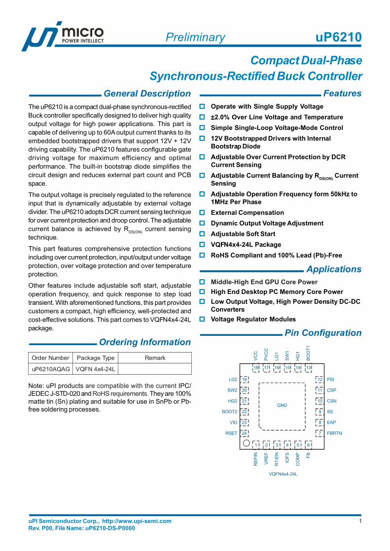
Pin Configuration
Note: uPI products are compatible with the current IPC/JEDEC J-STD-020 and RoHS requirements. They are 100%matte tin (Sn) plating and suitable for use in SnPb or Pb-free soldering processes.
VQFN4x4-24L
BOOT2
4321
LG1
HG
1
RT/
EN
VID
CSN
FB
VR
EF
HG2
SW2
GND10
9
8
7
21
22
23
24
17 16 1518
5
SW
1
11
SS
14
20
VC
C
6
12
13
19
CSP
RE
FIN
CO
MP
PVC
C
PSI
EAP
IOFS
RSET
LG2
BO
OT1
FBRTN
uPI Semiconductor Corp., http://www.upi-semi.comRev. P00, File Name: uP6210-DS-P0000
uP6210
2
Preliminary
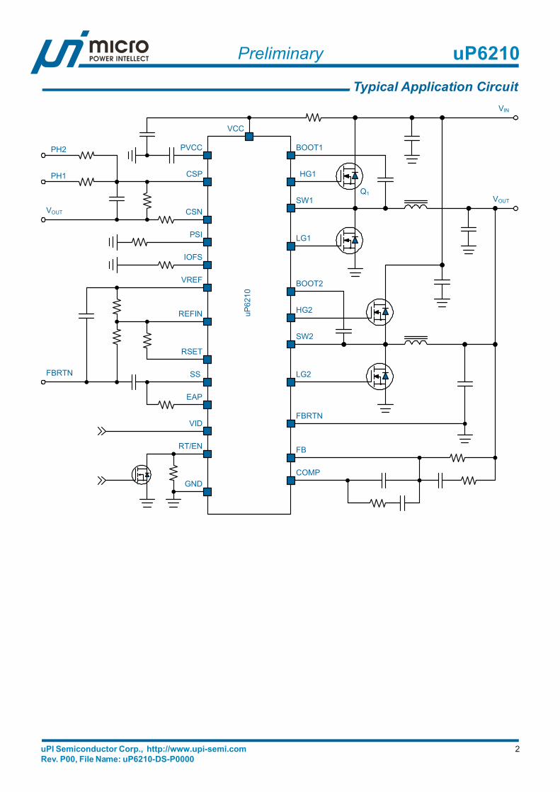
Typical Application Circuit
Q1
uP62
10
VCC
CSP
CSN
PH1
PH2
PSI
VREF
IOFS
REFIN
FB
COMP
FBRTN
PVCC
EAP
RT/EN
SS
GND
VIN
VOUT
VOUT
RSET
VID
FBRTN
BOOT1
HG1
SW1
LG1
BOOT2
HG2
SW2
LG2
uPI Semiconductor Corp., http://www.upi-semi.comRev. P00, File Name: uP6210-DS-P0000
uP6210
3
Preliminary
.oN emaNniP noitcnuFniP
1 NIFER .tupnIecnerefeRlanretxE redividegatlovatcennoC.egatlovecnereferlanretxefoniptupnisisihT.egatlovecnereferehttesotNTRBFotNIFERotFERVmorf
2 FERV .egatloVecnerefeRroftuptuO .egatlovecnereferV2noisicerphgihfoniptuptuoehtsisihT.NTRBFotroticapaccimarecFu1ahtiwnipsihtssapyB
3 NE/TR .gnitteSycneuqerFnoitarepO ehttesotDNGdnanipsihtneewtebrotsiseragnitcennoC.0126PuehtnwodtuhsotdnuorgotnipsihtlluP.ycneuqerfnoitarepo
4 SFOI .tnemtsujdAecnalaBtnerruC ehttsujdaotDNGroFERVotnipsihtmorfrotsiseratcennoC.gnirahstnerruc
5 PMOC.tuptuOreifilpmArorrE fotupnignitrevni-nonehtdna)AE(reifilpmarorreehtfotuptuoehtsisihT
-egatlovehtetasnepmocotnipBFehthtiwnoitanibmocninipsihtesU.srotarapmocMWPeht.retrevnocehtfopoolkcabdeeflortnoc
6 BF .egatloVkcabdeeF noitanibmocninipsihtesU.reifilpmarorreehtottupnignitrevniehtsinipsihT.retrevnocehtfopoolkcabdeeflortnocegatlovehtetasnepmocotnipPMOCehthtiw
7 NTRBF .nruteRkcabdeeF .detalugerebotsiegatlovtuptuoehterehwnipdnuogehtotnipsihttcennoC
8 PAE .reifilpmArorrEfotupnIgnitrevnI-noN .epolspoordehttesotnipSSotrotsiseratcennoC
9 SS .tuptuOtratStfoS .lavretnitratstfosehttesotNTRBFotroticapacatcennoC
01 NSC .reifilpmAgnisneStnerruCroftupnIevitageN
11 PSC .reifilpmAgnisneStnerruCroftupnIevitisoP
21 ISP.edoMgnivaSrewoP dlohserhtedomgnivasrewopehttesotDNGotISPmorfrotsiseratcennoC
rofdnuorgotnipsihttrohS.noitarepoesahpowtsyawlarofFERVotnipsihttcennoC.leveltnerruc.noitarepoesahpelgnissyawla
31 1TOOB ylppuSpartstooB roticapacpartstoobehttcennoC.1lennahcforevirdetagreppugnitaolfehtrofC TOOB .tiucricpartstoobamrofotnip1WSehtdnanip1TOOBneewteb
41 1GH.1lennahCroftuptuOrevirDetaGreppU sihT.TEFSOMreppufoetagehtotnipsihttcennoC
reppuehtnehwenimretedotyrtiucricnoitcetorphguorht-toohsevitpadaehtybderotinomsinip.ffodenrutsahTEFSOM
51 1WS
.1lennahCrofedoNhctiwS niardehtdnaTEFSOMreppuehtfoecruosehtotnipsihttcennoCderotinomoslasinipsihT.revirdETAGUehtrofknisehtsadesusinipsihT.TEFSOMrewolehtfodenrutsahTEFSOMreppuehtnehwenimretedotyrtiucricnoitcetorphguorht-toohsevitpadaehtyb
.ffo
61 1GL.1lennahCroftuptuOrevirDetaGrewoL sihT.TEFSOMrewolfoetagehtotnipsihttcennoC
rewolehtnehwenimretedotyrtiucricnoitcetorphguorht-toohsevitpadaehtybderotinomsinip.ffodenrutsahTEFSOM
71 CCVP .revirDetaGrofegatloVylppuS tnerrucsedivorpnipsihT.ODLV9lanretnifotuptuoehtsinipsihT.roticapaccimarecFu1muminimahtiwnipsihtssapyB.sevirdetagrof
81 CCV .egatloVylppuS nipsihtessapyB.ODLV9dnatiucriclortnoclanretniroftnerrucsedivorpnipsihT.CIehtottxenroticapaccimarecFu1muminimahtiw
Functional Pin Description
uPI Semiconductor Corp., http://www.upi-semi.comRev. P00, File Name: uP6210-DS-P0000
uP6210
4
Preliminary
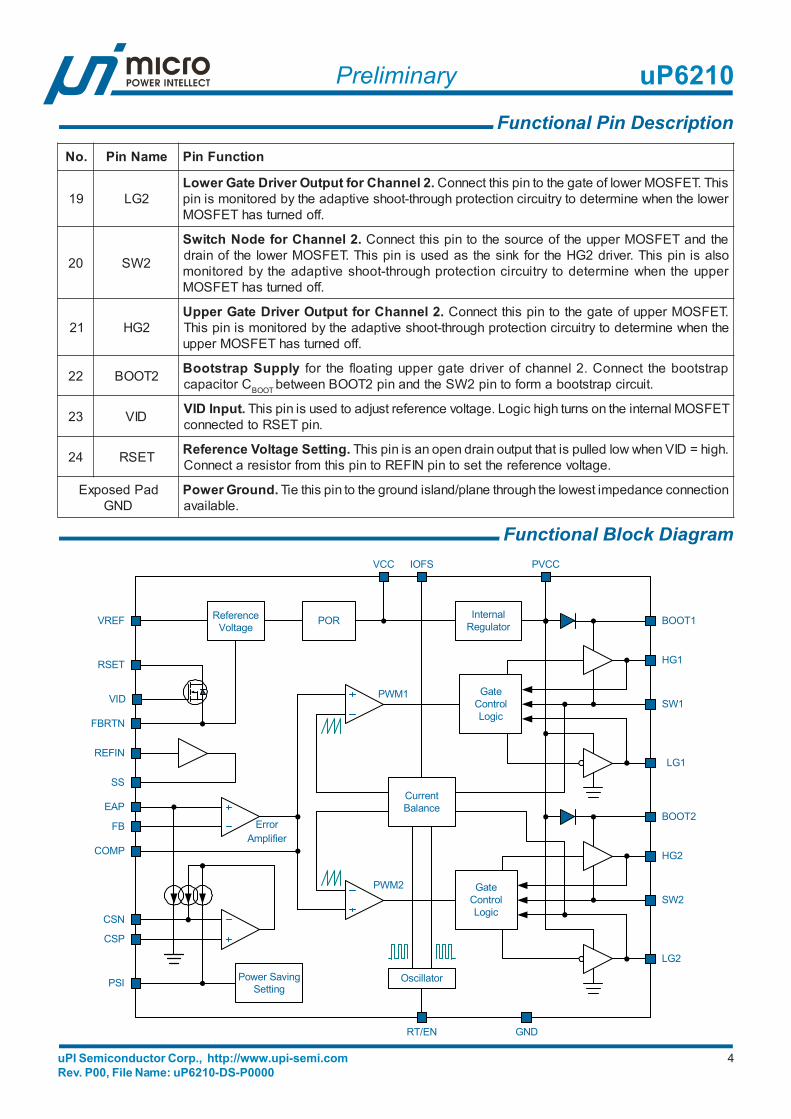
Functional Block Diagram
.oN emaNniP noitcnuFniP
91 2GL.2lennahCroftuptuOrevirDetaGrewoL sihT.TEFSOMrewolfoetagehtotnipsihttcennoC
rewolehtnehwenimretedotyrtiucricnoitcetorphguorht-toohsevitpadaehtybderotinomsinip.ffodenrutsahTEFSOM
02 2WS
.2lennahCrofedoNhctiwS ehtdnaTEFSOMreppuehtfoecruosehtotnipsihttcennoCoslasinipsihT.revird2GHehtrofknisehtsadesusinipsihT.TEFSOMrewolehtfoniardreppuehtnehwenimretedotyrtiucricnoitcetorphguorht-toohsevitpadaehtybderotinom
.ffodenrutsahTEFSOM
12 2GH.2lennahCroftuptuOrevirDetaGreppU .TEFSOMreppufoetagehtotnipsihttcennoC
ehtnehwenimretedotyrtiucricnoitcetorphguorht-toohsevitpadaehtybderotinomsinipsihT.ffodenrutsahTEFSOMreppu
22 2TOOB ylppuSpartstooB partstoobehttcennoC.2lennahcforevirdetagreppugnitaolfehtrofCroticapac TOOB .tiucricpartstoobamrofotnip2WSehtdnanip2TOOBneewteb
32 DIV .tupnIDIV TEFSOMlanretniehtnosnruthgihcigoL.egatlovecnerefertsujdaotdesusinipsihT.nipTESRotdetcennoc
42 TESR .gnitteSegatloVecnerefeR .hgih=DIVnehwwoldellupsitahttuptuoniardneponasinipsihT.egatlovecnereferehttesotnipNIFERotnipsihtmorfrotsiseratcennoC
daPdesopxEDNG
.dnuorGrewoP iT noitcennocecnadepmitsewolehthguorhtenalp/dnalsidnuorgehtotnipsihte.elbaliava
Functional Pin Description
GateControlLogic
PWM2
AmplifierError
Oscillator
PWM1
Current Balance
VREF BOOT1
HG1
SW1
LG1
BOOT2
HG2
SW2
LG2
Reference Voltage
VCC
REFIN
PVCC
Internal Regulator
GateControlLogic
POR
SS
FBRTN
EAP
FB
COMP
CSN
CSP
PSI
VID
RSET
IOFS
RT/EN GND
Power Saving Setting
uPI Semiconductor Corp., http://www.upi-semi.comRev. P00, File Name: uP6210-DS-P0000
uP6210
5
Preliminary
The uP6210 is a compact dual-phase synchronous-rectifiedBuck controller specifically designed to deliver high qualityoutput voltage for high power applications. This part iscapable of delivering up to 60A output current thanks to itsembedded bootstrapped drivers that support 12V + 12Vdriving capability. The uP6210 features configurable gatedriving voltage for maximum efficiency and optimalperformance. The built-in bootstrap diode simplifies thecircuit design and reduces external part count and PCBspace.
The output voltage is precisely regulated to the referenceinput that is dynamically adjustable by external voltagedivider. The uP6210 adopts DCR current sensing techniquefor over current protection and droop control. The adjustablecurrent balance is achieved by RDS(ON) current sensingtechnique.
This part features comprehensive protection functionsincluding over current protection, input/output under voltageprotection, over voltage protection and over temperatureprotection.
Other features include adjustable soft start, adjustableoperation frequency, and quick response to step loadtransient. With aforementioned functions, this part providescustomers a compact, high efficiency, well-protected andcost-effective solutions. This part comes to VQFN4x4-24Lpackage.
Power On Reset and InitializationThe uP6210 works with a single supply voltage at VCCpin. The VCC voltage is continuously monitored for poweron reset (POR) to ensure the supply voltage is high enoughfor normal operation of the device. The POR threshold levelis typically 9V at VCC rising.
9V LDO for Gate DriversThe uP6210 provides flexible gate driving voltage formaximum efficiency and optimal performance. A linearregulator provides 9V voltage at PVCC pin for gate drives.9V driving voltage reduces the power dissipation at uP6210to an acceptable level at large gate capacitance and highswitching frequency applications. Bootstrap diodes areembedded to facilitates PCB design and reduce the totalBOM cost. No external Schottky diode is required.
Chip Enable Oscillation Frequency Programming
A resistor RRT connected to RT pin programs the oscillationfrequency as:
)k(R10000fRT
OSC Ω= (kHz)
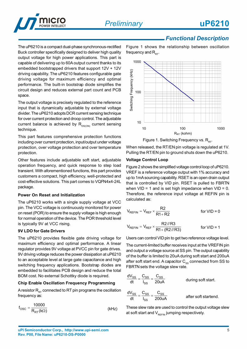
Functional DescriptionFigure 1 shows the relationship between oscillationfrequency and RRT.
10
100
1000
10 100 1000RRT (kohm)
Switc
hing
Fre
quen
cy (k
Hz)
Figure 1. Switching Frequency vs. RRT.
When released, the RT/EN pin voltage is regulated at 1V.Pulling the RT/EN pin to ground shuts down the uP6210.
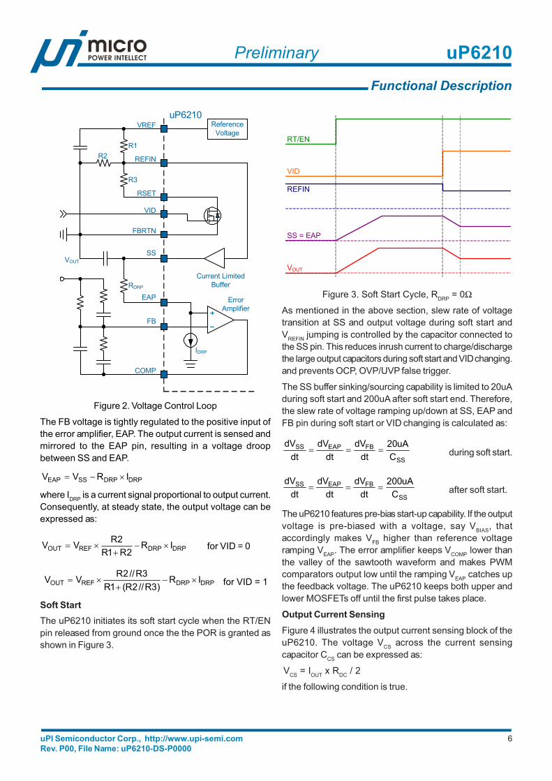
Voltage Control LoopFigure 2 shows the simplified voltage control loop of uP6210.VREF is a reference voltage output with 1% accuracy andup to 1mA sourcing capability. RSET is an open drain outputthat is controlled by VID pin. RSET is pulled to FBRTNwhen VID = 1 and is set high impedance when VID = 0.Therefore, the reference input voltage at REFIN pin iscalculated as:
2R1R2RVV REFREFIN +
×= for VID = 0
)3R//2R(1R3R//2RVV REFREFIN +
×= for VID = 1
Users can control VID pin to get two reference voltage level.
The current-limited buffer receives input at the VREFIN pinand output a voltage source at SS pin. The output capabilityof the buffer is limited to 20uA during soft start and 200uAafter soft start end. A capacitor CSS connected from SS toFBRTN sets the voltage slew rate.
uA20C
IC
dtdV SS
SS
SSSS == during soft start.
uA200C
IC
dtdV SS
SS
SSSS == after soft startend.
These slew rate are used to control the output voltage slewat soft start and VREFIN jumping respectively.
uPI Semiconductor Corp., http://www.upi-semi.comRev. P00, File Name: uP6210-DS-P0000
uP6210
6
Preliminary
Functional Description
ReferenceVoltage
SS
VREF
REFIN
uP6210
Current Limited Buffer
EAP
FB
COMP
VOUT
Error Amplifier
IDRP
RDRP
FBRTN
R1R2
VID
RSET
R3
Figure 2. Voltage Control Loop
The FB voltage is tightly regulated to the positive input ofthe error amplifier, EAP. The output current is sensed andmirrored to the EAP pin, resulting in a voltage droopbetween SS and EAP.
DRPDRPSSEAP IRVV ×−=
where IDRP is a current signal proportional to output current.Consequently, at steady state, the output voltage can beexpressed as:
DRPDRPREFOUT IR2R1R
2RVV ×−+
×= for VID = 0
DRPDRPREFOUT IR)3R//2R(1R
3R//2RVV ×−+
×= for VID = 1
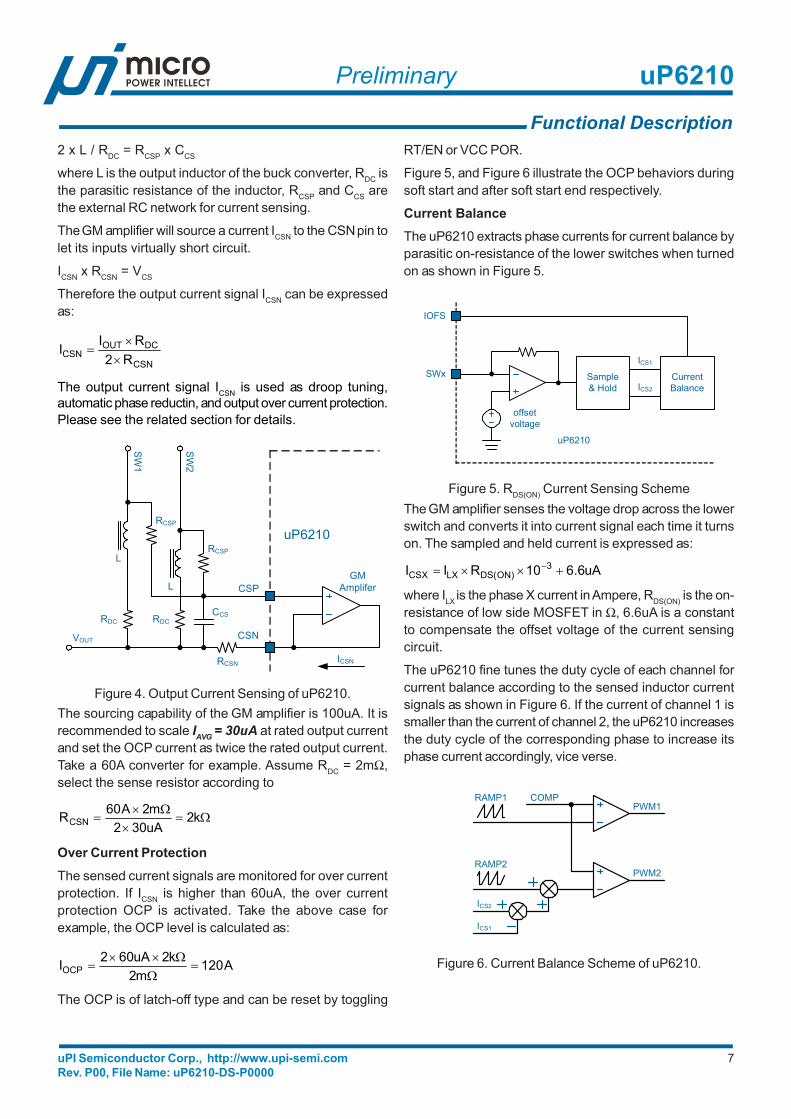
Soft StartThe uP6210 initiates its soft start cycle when the RT/ENpin released from ground once the the POR is granted asshown in Figure 3.
VID
REFIN
SS = EAP
VOUT
RT/EN
Figure 3. Soft Start Cycle, RDRP = 0Ω
As mentioned in the above section, slew rate of voltagetransition at SS and output voltage during soft start andVREFIN jumping is controlled by the capacitor connected tothe SS pin. This reduces inrush current to charge/dischargethe large output capacitors during soft start and VID changing.and prevents OCP, OVP/UVP false trigger.
The SS buffer sinking/sourcing capability is limited to 20uAduring soft start and 200uA after soft start end. Therefore,the slew rate of voltage ramping up/down at SS, EAP andFB pin during soft start or VID changing is calculated as:
SS
FBEAPSS
CuA20
dtdV
dtdV
dtdV
=== during soft start.
SS
FBEAPSS
CuA200
dtdV
dtdV
dtdV
=== after soft start.
The uP6210 features pre-bias start-up capability. If the outputvoltage is pre-biased with a voltage, say VBIAS, thataccordingly makes VFB higher than reference voltageramping VEAP. The error amplifier keeps VCOMP lower thanthe valley of the sawtooth waveform and makes PWMcomparators output low until the ramping VEAP catches upthe feedback voltage. The uP6210 keeps both upper andlower MOSFETs off until the first pulse takes place.
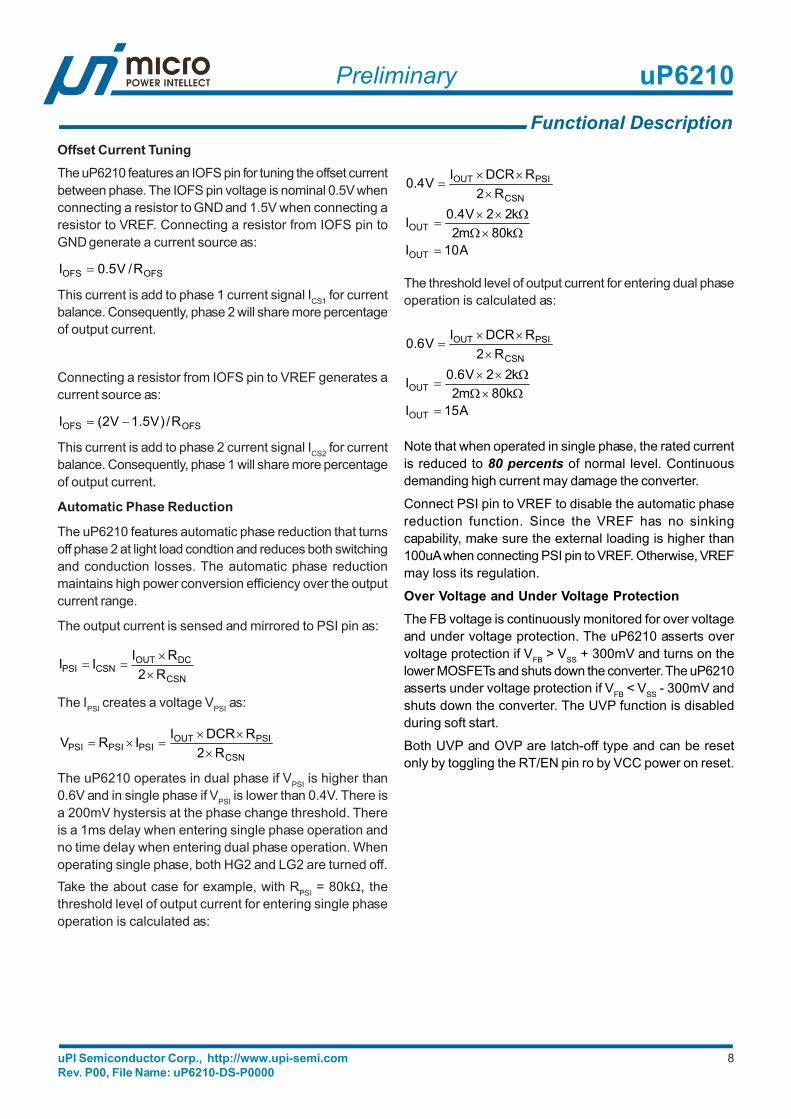
Output Current SensingFigure 4 illustrates the output current sensing block of theuP6210. The voltage VCS across the current sensingcapacitor CCS can be expressed as:
VCS = IOUT x RDC / 2
if the following condition is true.
uPI Semiconductor Corp., http://www.upi-semi.comRev. P00, File Name: uP6210-DS-P0000
uP6210
7
Preliminary
2 x L / RDC = RCSP x CCS
where L is the output inductor of the buck converter, RDC isthe parasitic resistance of the inductor, RCSP and CCS arethe external RC network for current sensing.
The GM amplifier will source a current ICSN to the CSN pin tolet its inputs virtually short circuit.
ICSN x RCSN = VCS
Therefore the output current signal ICSN can be expressedas:
CSN
DCOUTCSN R2
RII××
=
The output current signal ICSN is used as droop tuning,automatic phase reductin, and output over current protection.Please see the related section for details.
VOUT
CSP
CSN
SW1
SW2
ICSN
uP6210
RCSN
CCSRDCRDC
L
L
RCSP
RCSP
GMAmplifer
Figure 4. Output Current Sensing of uP6210.The sourcing capability of the GM amplifier is 100uA. It isrecommended to scale IAVG = 30uA at rated output currentand set the OCP current as twice the rated output current.Take a 60A converter for example. Assume RDC = 2mΩ,select the sense resistor according to
Ω=×
Ω×= k2
uA302m2A60RCSN
Over Current Protection
The sensed current signals are monitored for over currentprotection. If ICSN is higher than 60uA, the over currentprotection OCP is activated. Take the above case forexample, the OCP level is calculated as:
A120m2
k2uA602IOCP =Ω
Ω××=
The OCP is of latch-off type and can be reset by toggling
RT/EN or VCC POR.
Figure 5, and Figure 6 illustrate the OCP behaviors duringsoft start and after soft start end respectively.
Current BalanceThe uP6210 extracts phase currents for current balance byparasitic on-resistance of the lower switches when turnedon as shown in Figure 5.
SWx Sample & Hold
Current Balance
ICS1
ICS2
IOFS
uP6210
offset voltage
Figure 5. RDS(ON) Current Sensing SchemeThe GM amplifier senses the voltage drop across the lowerswitch and converts it into current signal each time it turnson. The sampled and held current is expressed as:
uA6.610RII 3)ON(DSLXCSX +××= −
where ILX is the phase X current in Ampere, RDS(ON) is the on-resistance of low side MOSFET in Ω, 6.6uA is a constantto compensate the offset voltage of the current sensingcircuit.
The uP6210 fine tunes the duty cycle of each channel forcurrent balance according to the sensed inductor currentsignals as shown in Figure 6. If the current of channel 1 issmaller than the current of channel 2, the uP6210 increasesthe duty cycle of the corresponding phase to increase itsphase current accordingly, vice verse.
ICS2
ICS1
PWM1
PWM2
COMPRAMP1
RAMP2
Figure 6. Current Balance Scheme of uP6210.
Functional Description
uPI Semiconductor Corp., http://www.upi-semi.comRev. P00, File Name: uP6210-DS-P0000
uP6210
8
Preliminary
Functional DescriptionOffset Current TuningThe uP6210 features an IOFS pin for tuning the offset currentbetween phase. The IOFS pin voltage is nominal 0.5V whenconnecting a resistor to GND and 1.5V when connecting aresistor to VREF. Connecting a resistor from IOFS pin toGND generate a current source as:
OFSOFS R/V5.0I =
This current is add to phase 1 current signal ICS1 for currentbalance. Consequently, phase 2 will share more percentageof output current.
Connecting a resistor from IOFS pin to VREF generates acurrent source as:
OFSOFS R/)V5.1V2(I −=
This current is add to phase 2 current signal ICS2 for currentbalance. Consequently, phase 1 will share more percentageof output current.
Automatic Phase Reduction
The uP6210 features automatic phase reduction that turnsoff phase 2 at light load condtion and reduces both switchingand conduction losses. The automatic phase reductionmaintains high power conversion efficiency over the outputcurrent range.
The output current is sensed and mirrored to PSI pin as:
CSN
DCOUTCSNPSI R2
RIII××
==
The IPSI creates a voltage VPSI as:
CSN
PSIOUTPSIPSIPSI R2
RDCRIIRV×
××=×=
The uP6210 operates in dual phase if VPSI is higher than0.6V and in single phase if VPSI is lower than 0.4V. There isa 200mV hystersis at the phase change threshold. Thereis a 1ms delay when entering single phase operation andno time delay when entering dual phase operation. Whenoperating single phase, both HG2 and LG2 are turned off.Take the about case for example, with RPSI = 80kΩ, thethreshold level of output current for entering single phaseoperation is calculated as:
A10Ik80m2k22V4.0I
R2RDCRIV4.0
OUT
OUT
CSN
PSIOUT
=Ω×ΩΩ××
=
×××
=
The threshold level of output current for entering dual phaseoperation is calculated as:
A15Ik80m2k22V6.0I
R2RDCRIV6.0
OUT
OUT
CSN
PSIOUT
=Ω×ΩΩ××
=
×××
=
Note that when operated in single phase, the rated currentis reduced to 80 percents of normal level. Continuousdemanding high current may damage the converter.
Connect PSI pin to VREF to disable the automatic phasereduction function. Since the VREF has no sinkingcapability, make sure the external loading is higher than100uA when connecting PSI pin to VREF. Otherwise, VREFmay loss its regulation.
Over Voltage and Under Voltage ProtectionThe FB voltage is continuously monitored for over voltageand under voltage protection. The uP6210 asserts overvoltage protection if VFB > VSS + 300mV and turns on thelower MOSFETs and shuts down the converter. The uP6210asserts under voltage protection if VFB < VSS - 300mV andshuts down the converter. The UVP function is disabledduring soft start.
Both UVP and OVP are latch-off type and can be resetonly by toggling the RT/EN pin ro by VCC power on reset.
uPI Semiconductor Corp., http://www.upi-semi.comRev. P00, File Name: uP6210-DS-P0000
uP6210
9
Preliminary
retemaraP lobmyS snoitidnoCtseT niM pyT xaM stinU
tupnIylppuS
egatloVylppuS V 21CC 5.4 -- 2.31 V
tnerruCylppuS I CCV;nepOGLdnaGH CC ,V21=
gnihctiwS -- 5 -- Am
tnerruCylppuStnecseiuQ I Q_CC I,gnihctiwSoN CCP Am0= -- 4 -- Am
egatloVylppuSdetalugeR V CCP I,V0=NE/TR CCP Am0= 8 9 01 V
dlohserhTROP V HTRCC 8 9 01 V
siseretsyHROP V SYHCC -- 0.1 -- V
gnitteSycneuqerF/elbanEpihC
tnerruCgnicruoSNE/TR I NE/TR .DNG=NE/TR 001 051 002 Au
egatloVNE/TR V NE/TR R NE/TR k33= Ω -- 1 -- V
egnaRgnitteSycneuqerFgnihctiwS 05 -- 0001 zHk
ycneuqerFgnihctiwSnuReerF f CSO R NE/TR k33= Ω 072 003 033 zHk
ycaruccAycneuqerFgnihctiwS ∆f CSO f CSO zHk005~zHk002= 51- -- 51 %
Supply Input Voltage, VCC (Note 1) --------------------------------------------------------------------------------------------- -0.3V to +15VSW to GND
DC ------------------------------------------------------------------------------------------------------------------------------------- -0.3V to 15V< 200ns ---------------------------------------------------------------------------------------------------------------------------- -5V to 30V
BOOT to SW -------------------------------------------------------------------------------------------------------------------------------------- 15VBOOT to GND
DC ------------------------------------------------------------------------------------------------------------------------- -0.3V to PHASE +15V< 200ns -------------------------------------------------------------------------------------------------------------------------- -0.3V to 42V
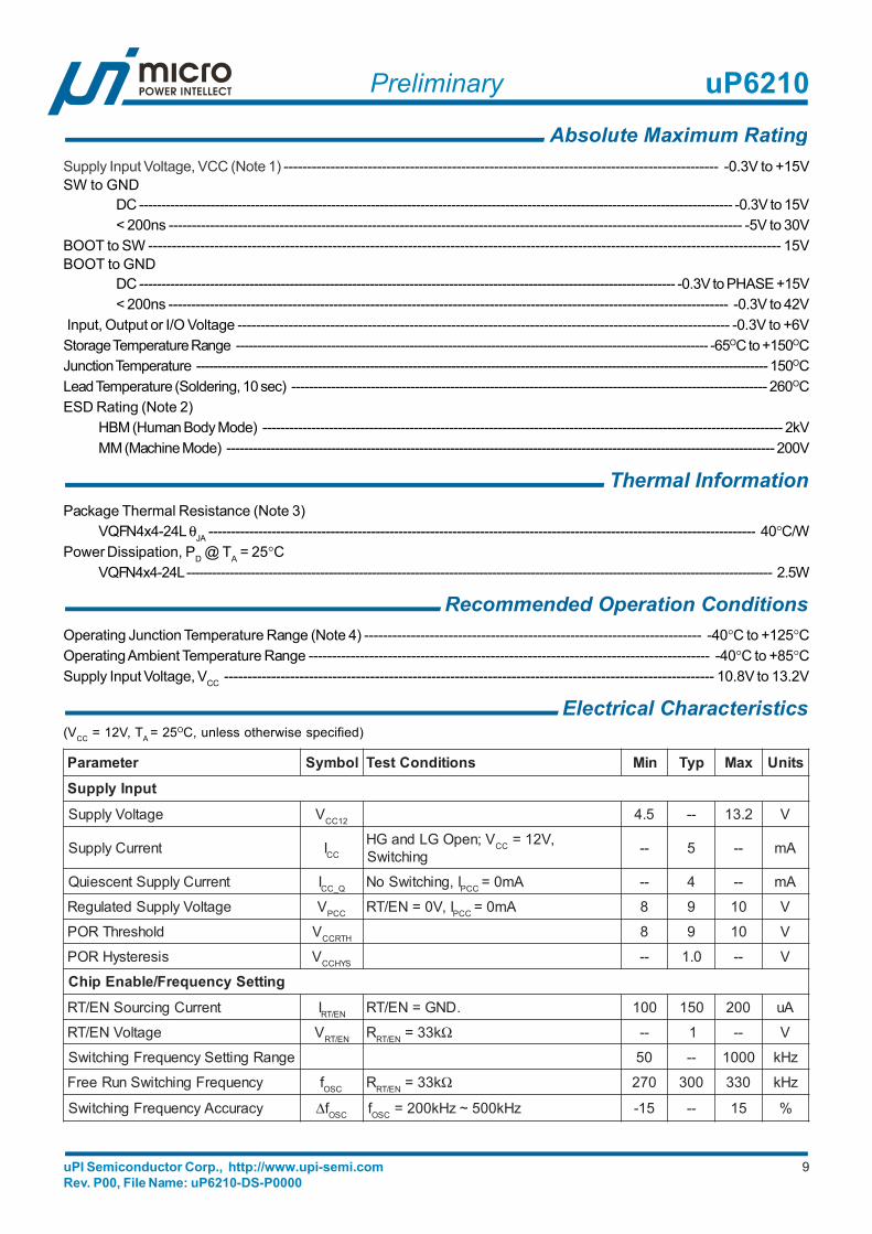
Input, Output or I/O Voltage ---------------------------------------------------------------------------------------------------------- -0.3V to +6VStorage Temperature Range ------------------------------------------------------------------------------------------------------------- -65OC to +150OCJunction Temperature ------------------------------------------------------------------------------------------------------------------------------------ 150OCLead Temperature (Soldering, 10 sec) ------------------------------------------------------------------------------------------------------------ 260OCESD Rating (Note 2)
HBM (Human Body Mode) --------------------------------------------------------------------------------------------------------------------- 2kVMM (Machine Mode) ----------------------------------------------------------------------------------------------------------------------------- 200V
Package Thermal Resistance (Note 3)VQFN4x4-24L θJA ------------------------------------------------------------------------------------------------------------------------- 40°C/W
Power Dissipation, PD @ TA = 25°CVQFN4x4-24L ---------------------------------------------------------------------------------------------------------------------------------------- 2.5W
Operating Junction Temperature Range (Note 4) ------------------------------------------------------------------------ -40°C to +125°COperating Ambient Temperature Range -------------------------------------------------------------------------------------- -40°C to +85°CSupply Input Voltage, VCC -------------------------------------------------------------------------------------------------------- 10.8V to 13.2V
Absolute Maximum Rating
Thermal Information
Recommended Operation Conditions
Electrical Characteristics(VCC = 12V, TA = 25OC, unless otherwise specified)
uPI Semiconductor Corp., http://www.upi-semi.comRev. P00, File Name: uP6210-DS-P0000
uP6210
10
Preliminary
Electrical CharacteristicsretemaraP lobmyS snoitidnoCtseT niM pyT xaM stinU
tratStfoS
tnerruCtratStfoS I SS .tratstfosgniruD -- 02 --Au
tnerruCylppuS I CC .dnetratstfosretfA -- 002 --
rotallicsO
elcyCytuDmumixaM -- 58 -- %
elcyCytuDmumixaM -- 0 -- %
edutilpmApmaR ∆V CSO V CC .V21= -- 5.3 -- V
edoMgnivaSrewoP
lauDgniretnErofegatloVdlohserhTesahP V ISP V ISP .gnisir 55.0 6.0 56.0 V
gniretnErofegatloVsiseretsyHesahPelgniS ∆V ISP V ISP .gnillaf -- 002 -- Vm
egatloVecnerefeR
ycaruccAegatloVecnerefeR V FER I FER Au001= 89.1 00.2 20.2 V
noitalugeRdaoLegatloVecnerefeR ∆V FER I FER Am2~0= 5- -- 5 Vm
ycaruccAegatloVtuptuO V BFV| NIFER V- BF V,| CC ,daoLoN,V21=R PRD 0= Ω V, NIFER .V6.1~V8.0= -- -- 5 Vm
reifilpmArorrE
niaGCDpooLnepO OA .ngisedybdeetnarauG 07 08 -- Bd
tcudorPhtdiwdnaB-niaG WBG C DAOL .ngisedybdeetnarauG,Fp5= 02 -- -- zHM
etaRwelS RS .ngisedybdeetnarauG 51 02 -- su/V
)ecruoS&kniS(tnerruCmumixaM I PMOC V PMOC V6.1= 5.1 0.2 -- Am
esneStnerruClatoT
tnerruCgnicruoSmumixaM I XAM_NSC 001 -- -- Au
tesffOreifilpmAMG 1- 0 1 Vm
dlohserhTnoitcetorPtnerruCrevOleveL I PCO_NSC -- 06 -- Au
ycaruccApoorD I PRD I/ NSC 09 001 011 %
ycaruccAISP I ISP I/ NSC 09 001 011 %
esneStnerruCesahP
ecnatcudnoc-snarT -- 0.1 -- Sm
egatloVSFOIV SFO k001 Ω FERVotSFOImorf -- 5.1 --
Vk001 Ω DNGotSFOImorf -- 5.0 --
uPI Semiconductor Corp., http://www.upi-semi.comRev. P00, File Name: uP6210-DS-P0000
uP6210
11
Preliminary
retemaraP lobmyS snoitidnoCtseT niM pyT xaM stinU
tupnIlortnoCDIV
leveLdlohserhThgiHcigoL V LI 2.1 -- -- V
leveLdlohserhTwoLcigoL V LI -- -- 4.0 V
TEFSOMTESRfoecnartsiseRnO R TESR hgiH=DIV -- 02 -- Ω
niPTESRfoegakaeL I TESR V TESER V0=DIV,V2= -- -- 1.0 Au
revirDetaG
gnicruoSetaGreppU R CRS_GH I GH gnicruosAm001= -- 2 4 Ω
gnikniSetaGreppU R KNS_GH I GH gniknisAm001= -- 5.1 3 Ω
ecruoSetaGrewoL R CRS_GL I GL gnicruosAm001= -- 2 4 Ω
kniSetaGrewoL R KNS_GL I GL gnikgnisAm001= -- 1 2 Ω
emiTdaeD T TD -- 03 -- sn
noitcetorP
noitcetorPegatloVrevO V BF V- SS -- 003 -- Vm
noitcetorPegatloVrednU V BF V- SS -- 003- -- Vm
noitcetorPerutarepmeTrevO -- 051 -- OC
siseretsyHerutarepmeTrevO -- 02 -- OC
Note 1. Stresses listed as the above “Absolute Maximum Ratings” may cause permanent damage to the device.These are for stress ratings. Functional operation of the device at these or any other conditions beyond thoseindicated in the operational sections of the specifications is not implied. Exposure to absolute maximumrating conditions for extended periods may remain possibility to affect device reliability.
Note 2. Devices are ESD sensitive. Handling precaution recommended.Note 3. θJA is measured in the natural convection at TA = 25°C on a low effective thermal conductivity test board of
JEDEC 51-3 thermal measurement standard.Note 4. The device is not guaranteed to function outside its operating conditions.
Electrical Characteristics
uPI Semiconductor Corp., http://www.upi-semi.comRev. P00, File Name: uP6210-DS-P0000
uP6210
12
Preliminary
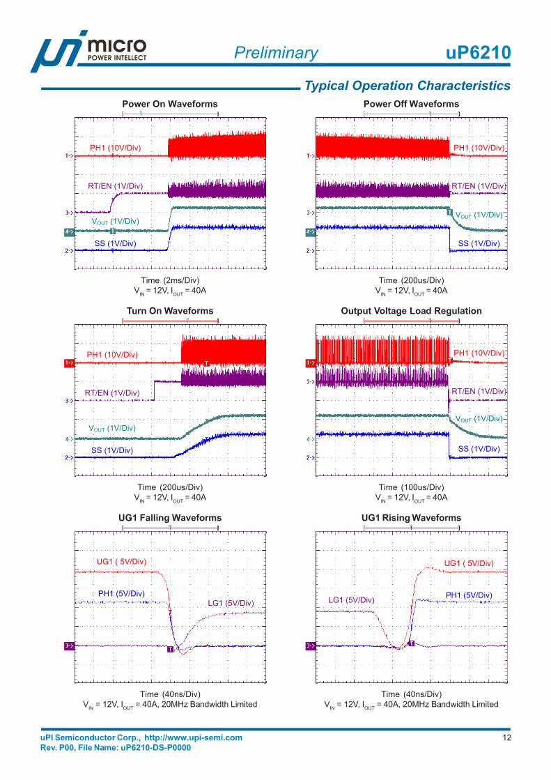
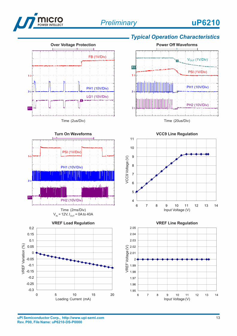
Typical Operation Characteristics
PH1 (10V/Div)
RT/EN (1V/Div)
SS (1V/Div)
VOUT (1V/Div)
PH1 (10V/Div)
RT/EN (1V/Div)
SS (1V/Div)
VOUT (1V/Div)
PH1 (10V/Div)
RT/EN (1V/Div)
SS (1V/Div)
VOUT (1V/Div)
PH1 (10V/Div)
RT/EN (1V/Div)
SS (1V/Div)
VOUT (1V/Div)
UG1 ( 5V/Div)
LG1 (5V/Div)PH1 (5V/Div)
UG1 ( 5V/Div)
LG1 (5V/Div) PH1 (5V/Div)
Power Off Waveforms
Time (200us/Div)VIN = 12V, IOUT = 40A
Power On Waveforms
Time (2ms/Div)VIN = 12V, IOUT = 40A
Turn On Waveforms
Time (200us/Div)VIN = 12V, IOUT = 40A
Output Voltage Load Regulation
Time (100us/Div)VIN = 12V, IOUT = 40A
UG1 Falling Waveforms
Time (40ns/Div)VIN = 12V, IOUT = 40A, 20MHz Bandwidth Limited
UG1 Rising Waveforms
Time (40ns/Div)VIN = 12V, IOUT = 40A, 20MHz Bandwidth Limited
uPI Semiconductor Corp., http://www.upi-semi.comRev. P00, File Name: uP6210-DS-P0000
uP6210
13
Preliminary
1.95
1.96
1.97
1.98
1.99
2
2.01
2.02
2.03
2.04
2.05
6 7 8 9 10 11 12 13 14
Typical Operation Characteristics
FB (1V/Div)
LG1 (10V/Div)
PH1 (10V/Div)
PSI (1V/Div)
PH2 (10V/Div)
PH1 (10V/Div)
VOUT (1V/Div)
PSI (1V/Div)
PH2 (10V/Div)
PH1 (10V/Div)
Power Off Waveforms
Time (20us/Div)
Over Voltage Protection
Time (2us/Div)
Turn On Waveforms
Time (2ms/Div)VIN = 12V, IOUT = 0A to 40A
4
5
6
7
8
9
10
11
6 7 8 9 10 11 12 13 14
VCC9 Line Regulation
Input Voltage (V)
VC
C9
Volta
ge (V
)
VREF Load Regulation
Loading Current (mA)
VRE
F Va
riatio
n (%
)
-0.3
-0.25
-0.2
-0.15
-0.1
-0.05
0
0.05
0.1
0.15
0.2
0 5 10 15 20
VREF Line Regulation
Input Voltage (V)
VREF
Vol
tage
(V)
uPI Semiconductor Corp., http://www.upi-semi.comRev. P00, File Name: uP6210-DS-P0000
uP6210
14
Preliminary
290
292
294
296
298
300
302
304
306
308
310
-50 -25 0 25 50 75 100 125
1.95
1.96
1.97
1.98
1.99
2
2.01
2.02
2.03
2.04
2.05
-50 -25 0 25 50 75 100 125
100
1000
1 10 100
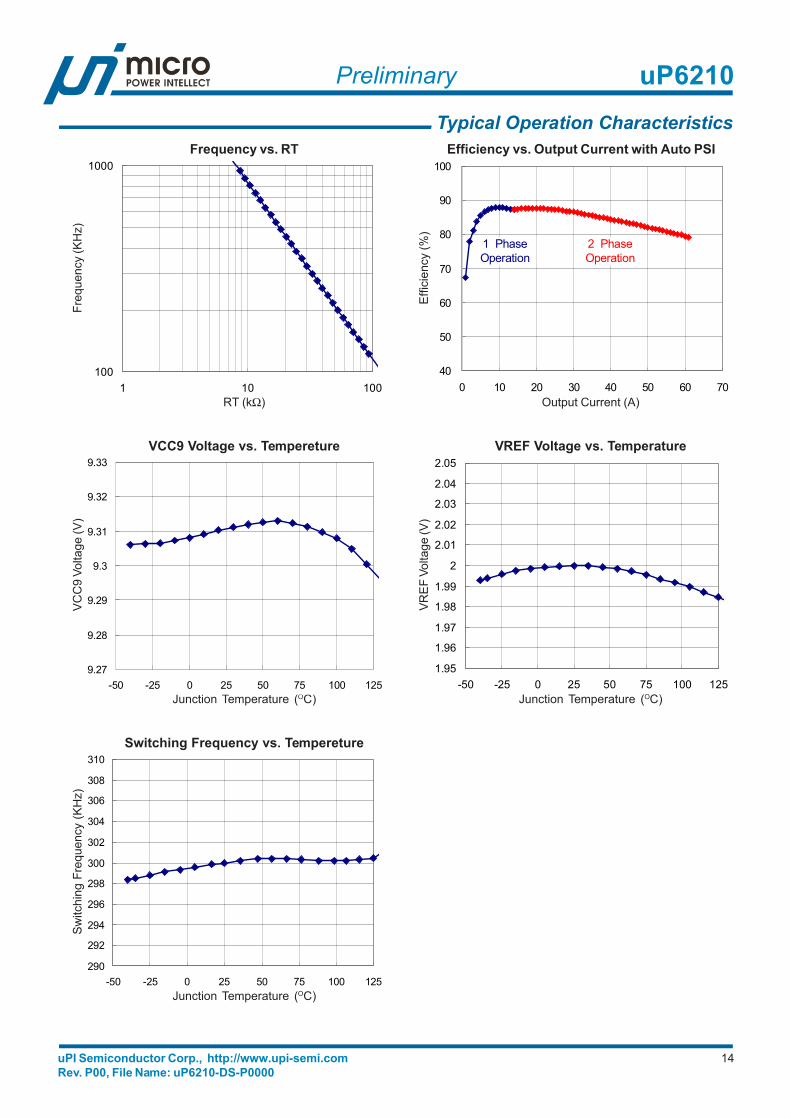
Typical Operation CharacteristicsFrequency vs. RT
RT (kΩ)
Freq
uenc
y (K
Hz)
Efficiency vs. Output Current with Auto PSI
Output Current (A)
Effi
cien
cy (%
)
VCC9 Voltage vs. Tempereture
Junction Temperature (OC)
VC
C9
Volta
ge (V
)
VREF Voltage vs. Temperature
Junction Temperature (OC)
VREF
Vol
tage
(V)
40
50
60
70
80
90
100
0 10 20 30 40 50 60 70
1 Phase Operation
2 Phase Operation
9.27
9.28
9.29
9.3
9.31
9.32
9.33
-50 -25 0 25 50 75 100 125
Switching Frequency vs. Tempereture
Junction Temperature (OC)
Sw
itchi
ng F
requ
ency
(KH
z)

uPI Semiconductor Corp., http://www.upi-semi.comRev. P00, File Name: uP6210-DS-P0000
uP6210
15
Preliminary
Application InformationFBRTN ConfigurationSince the reference voltage VREF is measured withrespective to FBRTN, connect circuits related to VREF,REFIN, and SS pin to FBRTN locally with short traces asshown in the Typical Application Circuit.
Total Current SensingIn the real application, PCB trances are not ideal and havecertain parasitic resistances RPCB1 and RPCB2 as shown inFigure 1. When these parasistic resistances are notidentical, the voltages at inductor terminals are not thesame, contributing meausrement error on total currentsensing. Two 1Ω resistors, connecting directly to inductorterminals are recommended to elimiate the effects ofparasitic resistance.
A 0.1uF capacitor CBYP is also recommended to bypassingnoise when the uP6210 is far away from the outputinductors. Place the CBYP physically near the IC.
VOUT
CSP
CSN
SW
1
SW
2ICSN
uP6210
RCSN
CCSRDC
L L
RCSPRCSP
GMAmplifer
RDC
RPCB1
RPCB2
1ohm
1ohmCBYP
Figure 1. Parasitic Resistance of PCB
uPI Semiconductor Corp., http://www.upi-semi.comRev. P00, File Name: uP6210-DS-P0000
uP6210
16
Preliminary
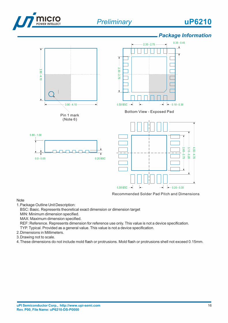
Package Information
Note1.Package Outline Unit Description:
BSC: Basic. Represents theoretical exact dimension or dimension targetMIN: Minimum dimension specified.MAX: Maximum dimension specified.REF: Reference. Represents dimension for reference use only. This value is not a device specification.TYP. Typical. Provided as a general value. This value is not a device specification.
2.Dimensions in Millimeters.3.Drawing not to scale.4.These dimensions do not include mold flash or protrusions. Mold flash or protrusions shell not exceed 0.15mm.
3.90 - 4.10
Pin 1 mark(Note 6)
Bottom View - Exposed Pad
2.65 - 2.75
2.30 - 2.750.18 - 0.30
2.30 - 2.75 0.35 - 0.453.10 - 3.20
4.50 - 4.70
3.90 - 4.10
0.0 - 0.05
0.80 - 1.00
0.20 BSC
Recommended Solder Pad Pitch and Dimensions
0.20 - 0.30