primary power supply device catalog ver.1
TRANSCRIPT
Ver.1.1
Primary Power Supply Device Catalog
A C / D C C o n v e r t e r
01 Primary Power Supply Device Catalog
Until now, product manufacturers primarily focused on application circuits
and secondary power supplies to improve set energy savings, but in recent
years to meet the need for higher efficiencies and lower power
consumption designers are beginning to look at primary power supplies as
well. In addition, laws and regulations such as Energy Star, CoC, and DoE
have spurred interest in power supply design.
ROHM proposes total solutions including power supply ICs and
peripheral discrete components that leverage our latest proprietary power
supply technologies. Ideal for advanced and next-generation primary
power supply systems requiring greater stability and safety.
Our primary power supply ICs integrate a number of circuit design
technologies to achieve high efficiency, low standby power and low noise.
ROHM offers a broad portfolio of ICs, discretes, and modules to meet
virtually any need. In addition, a variety of application support tools* are
available that allow users to verify the details of our product lineup and
the characteristics of the new power supply.
Examples
●X capacitor discharge circuit
●Ringing noise improvement circuit at light loads
●Low current shunt regulator
●Burst operation at light loads
●VCC recharge circuit
●Peak drive circuit
INDEX Product Overview (By Power Supply Topology)
ROHM's Complete Primary Power Supply Solution
Primary Power Supply Product Matrix
AC/DC Converter Product Development Policy
Built-in MOS series (Buck Converter Topology)
Built-in MOS series (PWM Flyback type Topology)
External MOS series
PFC series
Secondary Synchronous Rectification IC series
AC/DC series with Built-in SiC MOSFET
P.02
P.03
P.04
P.05
P.09
P.13
P.15
P.16
P.17
Technology Trends in Primary Power Supplies
*Refer to P20

02Primary Power Supply Device Catalog
To ensure high reliability along with other characteristics such as power supply block efficiency and standby power consumption, it is necessary to consider not only the IC itself but the entire power supply block as well, including discretes and other peripheral components. In addition to ICs and discretes, ROHM proposes total solutions that include peripheral components necessary to achieve the required reliability and power supply characteristics. Please consider this total power supply block circuit for your next design.
ROHM Offers Complete Solutions
IC
Discrete
Other
F1
C8
LF1
BD1D6
C11
R9
R7
R6R10C6
IC2PC1
14
C4R3
23
R8
R4 C2
D3
T1
C1
C20
4 1
5 7 8
AC IN
IN1
IN2
D
S
GND FB
VCC R5
C3
C7
D4
VOUT
GND
VOUT
IC1BM2P0**
4th Gen Fast Recovery Diodes (RFS/RFL series)
3rd Gen Fast Recovery Diodes (RFN/RFV series)
Zener Diodes
Shunt Resistors
High Reliability ResistorsProduct Features and Lineup
3rd Gen Trench-type SiC MOSFETs
3rd Gen SiC Schottky Barrier Diodes
2nd Gen Super Junction MOSFETs (600V/650V)
Circuit Diagram (By Topology)
PFC (Power Factor Correction) ICs
Application Support
ROHM Group Locations
P.18
P.20
P.20
P.21
P.23
P.25
P.29
P.30
P.31
P.33
P.35
P.37
Isolation Circuit Example
ROHM Proposes a Total Solution for an AC/DC Converter System
03 Primary Power Supply Device Catalog
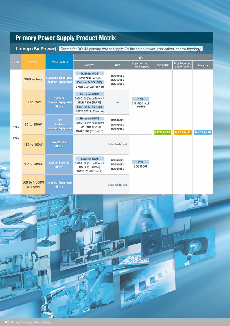
Primary Power Supply Product Matrix
Lineup (By Power)
PowerInput ApplicationsITEM
AC/DC PFCSynchronousRectification MOSFET
Fast Recovery/ Zener Diodes Resistor
30W or less Consumer ElectronicsIndustrial Equipment
Built-in MOS
BM2Pxxx seriesBuilt-in MOS (SiC)
BM2SCQ12xT series
BD7690FJ
BD7691FJ
BD7692FJ
BD7690FJ
BD7691FJ
BD7692FJ
BD7690FJ
BD7691FJ
BD7692FJ
30 to 75WPrinters
Industrial EquipmentOthers
External MOS
BM1Q104 (Pseudo-Resonant)BM1P101 (PWM)
Built-in MOS (SiC)
BM2SCQ12xT series
—
Under development
Under development
1ch
BM1R001xxF series
75 to 150WTVs
AudiosIndustrial Equipment
External MOS
BM1Q104 (Pseudo-Resonant)BM1P101 (PWM)
BM1C102 (PFC+QR)
150 to 300WLaser Printers
Others —
300 to 500W Gaming SystemsOthers
External MOS
BM1Q104 (Pseudo-Resonant)BM1P101 (PWM)
BM1C102 (PFC+QR)
2ch
BD85506F
500 to 1,000Wand over
Industrial EquipmentOthers
—
100V
200V
▶P.21 to 28 ▶P.29 to 32 ▶P.33 to 36
Search for ROHM primary power supply ICs based on power, application, and/or topology

04Primary Power Supply Device Catalog
This is perhaps the most important requirement for primary power supplies. Our AC/DC converter ICs feature a multi-chip configuration comprised of a high-voltage startup circuit, controller, and switching MOSFET.
ROHM’s total solution combining proprietary circuit technologies such as an X capacitor discharge function and built-in low current shunt regulator with discrete components contribute to lower set standby power consumption.
In addition to the built-in original SuperJunction MOSFET, ROHM leverages IC circuit current reduction, secondary synchronous rectification and other circuit technologies to meet market needs for greater efficiency.
3 Key Parameters (High Reliability • High Efficiency • Low Standby Power)
◆ Integrates ROHM’s 650V/800V MOSFET
◆ Original burst circuit for light loads
◆ High efficiency quasi-resonant circuit
◆ Secondary synchronous rectification
◆ X capacitor discharge circuit
◆ Low power startup circuit
◆ Low power circuit technology
The features and development policy of primary power supplies are high reliability, high efficiency, and low standby power consumption.
These 3 parameters are among the most in demand in recent years.
Separation betweenthe high-and low-voltage blocks
High reliability design resistant to external overvoltage and surge breakdown
②650V/800V Start-up Chip①650V/800V MOSFET
③Control IC
High Reliability
High Efficiency
Low StandbyPower
AC/DC Converter Product Development Policy
05 Primary Power Supply Device Catalog
InsertedComponents
Surface MountComponents
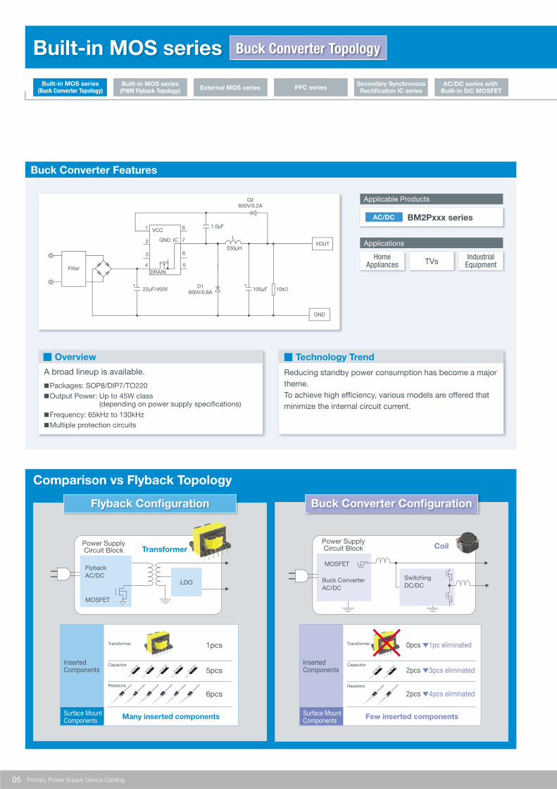
Buck Converter Features
Comparison vs Flyback Topology
A broad lineup is available.
■Packages: SOP8/DIP7/TO220■Output Power: Up to 45W class (depending on power supply specifications)■Frequency: 65kHz to 130kHz■Multiple protection circuits
■ Overview
Flyback Configuration Buck Converter Configuration
■ Technology Trend
Reducing standby power consumption has become a major theme. To achieve high efficiency, various models are offered that minimize the internal circuit current.
Power SupplyCircuit Block Transformer
FlybackAC/DC
MOSFET
LDO
Power SupplyCircuit Block Coil
SwitchingDC/DC
Buck ConverterAC/DC
MOSFET
Many inserted components Few inserted components
1pcs
5pcs
6pcs
0pcs ▼1pc eliminated
2pcs ▼3pcs eliminated
2pcs ▼4pcs eliminated
InsertedComponents
Surface MountComponents
Built-in MOS series
Built-in MOS series(Buck Converter Topology)
Built-in MOS series(PWM Flyback Topology) External MOS series PFC series
Secondary SynchronousRectification IC series
AC/DC series with Built-in SiC MOSFET
1
4 5
7
8VCC
GND_IC
DRAIN
22μF/450V D1600V/0.8A
D2600V/0.2A
L
6
2
3
Filter
330μH
100μF 10kΩ
1.0μF
VOUT
GND
Applicable Products
Applications
BM2Pxxx series
HomeAppliances
IndustrialEquipmentTVs
AC/DC
Buck Converter Topology
Transformer
Capacitor
Resistors
Capacitor
Resistors
Transformer
06Primary Power Supply Device Catalog
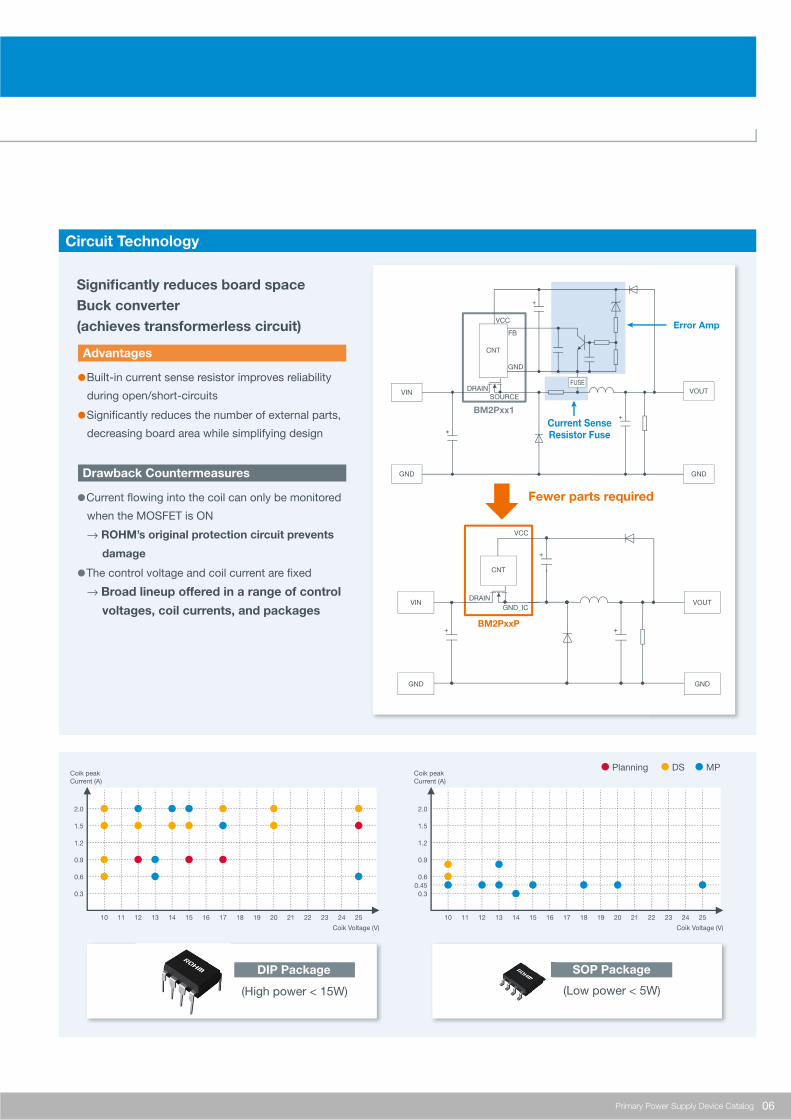
Circuit Technology
Significantly reduces board spaceBuck converter(achieves transformerless circuit)
●Built-in current sense resistor improves reliability
during open/short-circuits
●Significantly reduces the number of external parts,
decreasing board area while simplifying design
Fewer parts required
(High power < 15W) (Low power < 5W)
0.3
0.6
0.9
1.2
1.5
2.0
10 11 12 13 14 15 16 17 18 19 20 21 22 23 24 25
Coik peakCurrent (A)
Coik Voltage (V)
0.3
0.60.45
0.9
1.2
1.5
2.0
10 11 12 13 14 15 16 17 18 19 20 21 22 23 24 25
Coik peakCurrent (A)
Coik Voltage (V)
Planning DS MP
VIN
GND
VOUT
GND
CNT
DRAINGND_IC
VCC
BM2PxxP
DIP Package
Advantages
Drawback Countermeasures
SOP Package
●Current flowing into the coil can only be monitored
when the MOSFET is ON
→ ROHM’s original protection circuit prevents
damage
●The control voltage and coil current are fixed
→ Broad lineup offered in a range of control
voltages, coil currents, and packages
Current SenseResistor Fuse
Error Amp
VIN VOUT
GND
CNT
VCC
FB
GND
DRAINSOURCE
FUSE
BM2Pxx1
GND
07 Primary Power Supply Device Catalog
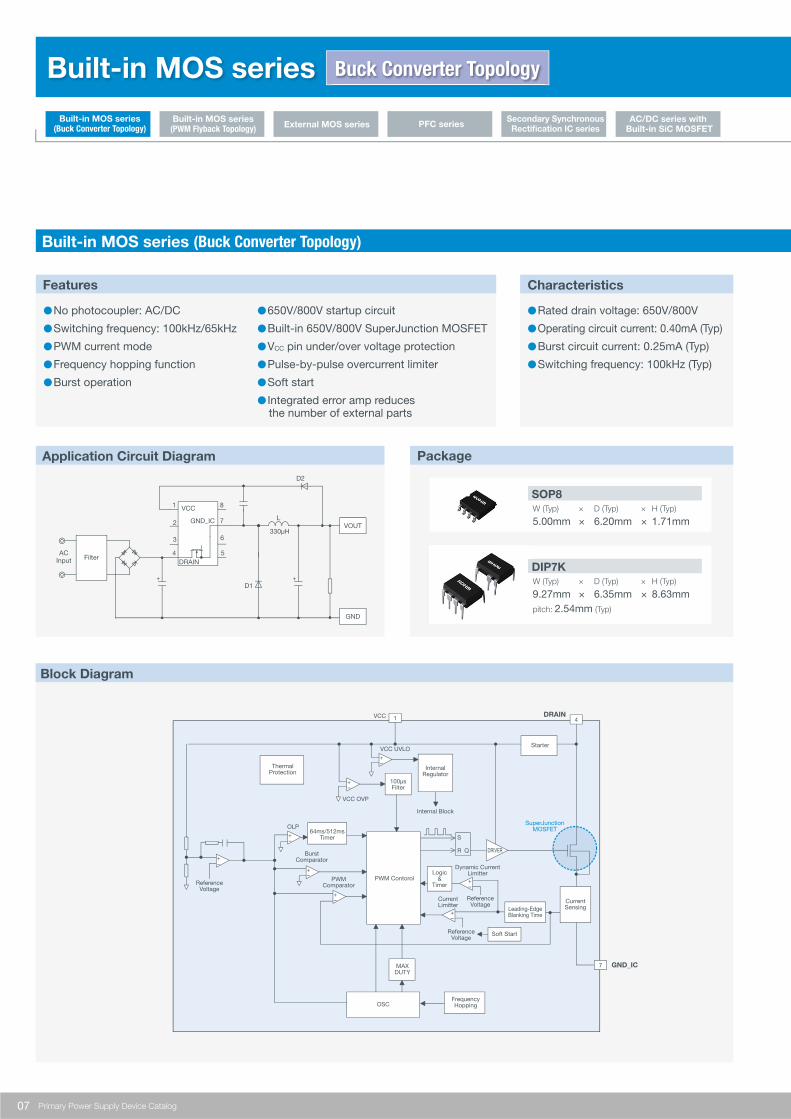
Built-in MOS series (Buck Converter Topology)
●No photocoupler: AC/DC
●Switching frequency: 100kHz/65kHz
●PWM current mode
●Frequency hopping function
●Burst operation
●Rated drain voltage: 650V/800V
●Operating circuit current: 0.40mA (Typ)
●Burst circuit current: 0.25mA (Typ)
●Switching frequency: 100kHz (Typ)
Characteristics
●650V/800V startup circuit
●Built-in 650V/800V SuperJunction MOSFET
●VCC pin under/over voltage protection
●Pulse-by-pulse overcurrent limiter
●Soft start
● Integrated error amp reduces the number of external parts
SOP8W (Typ) × D (Typ) × H (Typ)
5.00mm × 6.20mm × 1.71mm
DIP7KW (Typ) × D (Typ) × H (Typ)
9.27mm × 6.35mm × 8.63mmpitch: 2.54mm (Typ)
Features
Application Circuit Diagram Package
Block Diagram
S
QR
+–
7
41VCC
VCC UVLOStarter
DRAIN
VCC OVP
OLP64ms/512ms
Timer
BurstComparator
100μsFilter
InternalRegulator
Internal Block
DRIVER
SuperJunctionMOSFET
ThermalProtection
+–
+–
+–
+–
ReferenceVoltage
PWMComparator
+–
PWM Contorol
OSC
MAXDUTY
FrequencyHopping
ReferenceVoltage
CurrentLimitter
+–
ReferenceVoltage
+–
Dynamic CurrentLimitterLogic
&Timer
Soft Start
Leading-EdgeBlanking Time
CurrentSensing
GND_IC
1
4 5
7
8VCC
GND_IC
DRAIN
D1
D2
L
6
2
3
FilterAC
Input
330μHVOUT
GND
Built-in MOS series(Buck Converter Topology)
Built-in MOS series(PWM Flyback Topology) External MOS series PFC series
Secondary SynchronousRectification IC series
AC/DC series with Built-in SiC MOSFET
Built-in MOS series Buck Converter Topology
08Primary Power Supply Device Catalog
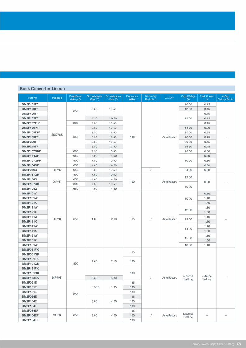
PackagePart No. BreakDownVoltage (V)
On resistanse(Typ) (Ω)
On resistanse(Max) (Ω)
Frequency(kHz)
FrequencyReduction VCC OVP Output Voltage
(V)Peak Current
(A)X-Cap.
Discharge Function
BM2P109TF
BM2P129TF
BM2P139TF
BM2P135TF
BM2P137TKF
BM2P159PF
BM2P159T1F
BM2P189TF
BM2P209TF
BM2P249TF
BM2P137QKF
BM2P134QF
BM2P107QKF
BM2P104QF
BM2P249Q
BM2P137QK
BM2P134Q
BM2P107QK
BM2P104Q
BM2P101V
BM2P101W
BM2P101X
BM2P121W
BM2P121X
BM2P131W
BM2P131X
BM2P141W
BM2P141X
BM2P151W
BM2P151X
BM2P181W
BM2P061FK
BM2P061GK
BM2P101FK
BM2P101GK
BM2P131FK
BM2P131GK
BM2P133EK
BM2P061E
BM2P101E
BM2P131E
BM2P064E
BM2P104E
BM2P134E
BM2P064EF
BM2P104EF
BM2P134EF
DIP7K
DIP7K
DIP7K
DIP7AK
SOP8
650
800
650
650 1.00
8001.60
3.30
0.955
3.00
3.00
650
650
800
650
800
650
650
800
650
800
650
9.50
4.50
7.50
9.50
9.50
9.50
9.50
9.50
7.50
4.00
7.50
4.00
9.50
7.50
4.00
7.50
4.00
2.00
2.15
4.80
1.35
4.00
4.00
12.50
6.50
10.50
12.50
12.50
12.50
12.50
12.50
10.50
4.50
10.50
4.50
12.50
10.50
4.50
10.50
4.50
10.00
12.00
13.00
14.20
15.00
18.00
20.00
24.80
13.00
10.00
24.80
13.00
10.00
0.80
10.00
12.00
13.00
14.00
15.00
18.00
0.45
0.45
0.45
0.45
0.45
0.30
0.45
0.45
0.45
0.45
0.80
0.80
0.80
0.80
0.80
0.80
1.10
1.50
1.10
1.50
1.10
1.50
1.10
1.50
1.10
1.50
1.10
SSOP8S
65
65
65
100
130
65
100
130
65
100
130
100
130
100
100
Auto Restart
Auto Restart
Auto Restart
ExternalSetting
ExternalSetting
External Setting
Auto Restart
Auto Restart
——
— —
—
—
— —
Buck Converter Lineup

09 Primary Power Supply Device Catalog
PowerLess than
70W
Less than25W
Time
650V starter650V MOSFET(Ron=1.4Ω)PWM typeFsw=65kHz
STBY<25mW
BM2P01xT
Low ON resistance
Low noise
High frequency
Original burst function
Input brown in/out
X capacitor discharge function
and more...
Next-Generation(Features)
650V/800V starter650V/800V MOSFETPWM typeFsw=65kHz
STBY<25mW
BM2Pxx1 series
650V/800V starter650V/800V MOSFETPWM typeFsw = 65kHz/100kHzFor non-isolated type
STBY<25mW
BM2PxxxP series
650V/800V starter650V/800V MOSFETPWM typeFsw=65kHz,100kHz,130kHz
STBY<25mW
BM2PxxxE series650V starter650V/800V MOSFETPWM typeFsw=100kHzX capacitor discharge function
STBY<15mW
BM2PxxxC series
1,700V 1.4ΩSiC MOSFET InsideQR Linear typeFsw=120kHz (Max)Compatible with 690VAC inputBuilt-in gate clamper circuit
▶P.17
BM2SCQ12xT series
Flyback
TO220-7
Flyback
DIP7SOP8
PWM Flyback Features
A broad lineup is available.
■Packages: SOP8/DIP7K/TO220■Output Power: Up to 45W class (depending on power supply specifications)■Frequency: 65kHz to 130kHz■Multiple protection circuits
■ Overview ■ Technology Trend
Reducing standby power has become a major theme. To achieve high efficiency, various models are offered featuring low circuit current.
F1
C8
LF1
BD1 D6
C11
R9
R7
R6R10C6
IC2PC1
14C4R3
23
R8
R4 C2
D3
T1
C1
C20
4 1
5 7 8
AC IN
IN1
IN2
D
SGND FB
VCC R5
C3
C7
D4
VOUT
GND
VOUT
AC/DC Converter Road Map (PWM Flyback Topology with Built-in MOSFET)
Buck
BM2Pxxx seriesAC/DC
Built-in MOS series(Buck Converter Topology)
Built-in MOS series(PWM Flyback Topology) External MOS series PFC series
Secondary SynchronousRectification IC series
AC/DC series with Built-in SiC MOSFET
Built-in MOS series PWM Flyback Topology
Applicable Products
Applications
HomeAppliances
IndustrialEquipmentTVs
10Primary Power Supply Device Catalog
Circuit Technology
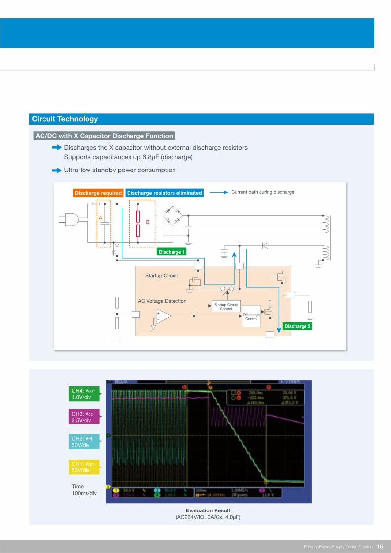
CH4: VOUT
1.0V/div
CH3: VCC
2.5V/div
CH2: VH50V/div
CH1: Vac50V/div
Time100ms/div
Evaluation Result(AC264V/IO=0A/Cx=4.0μF)
AC/DC with X Capacitor Discharge Function
Discharges the X capacitor without external discharge resistorsSupports capacitances up 6.8μF (discharge)
Ultra-low standby power consumption
Discharge required Discharge resistors eliminated Current path during discharge
DischargeControl
Startup CircuitControl
+–
Startup Circuit
AC Voltage Detection
Discharge 1
Discharge 2
AB
11 Primary Power Supply Device Catalog
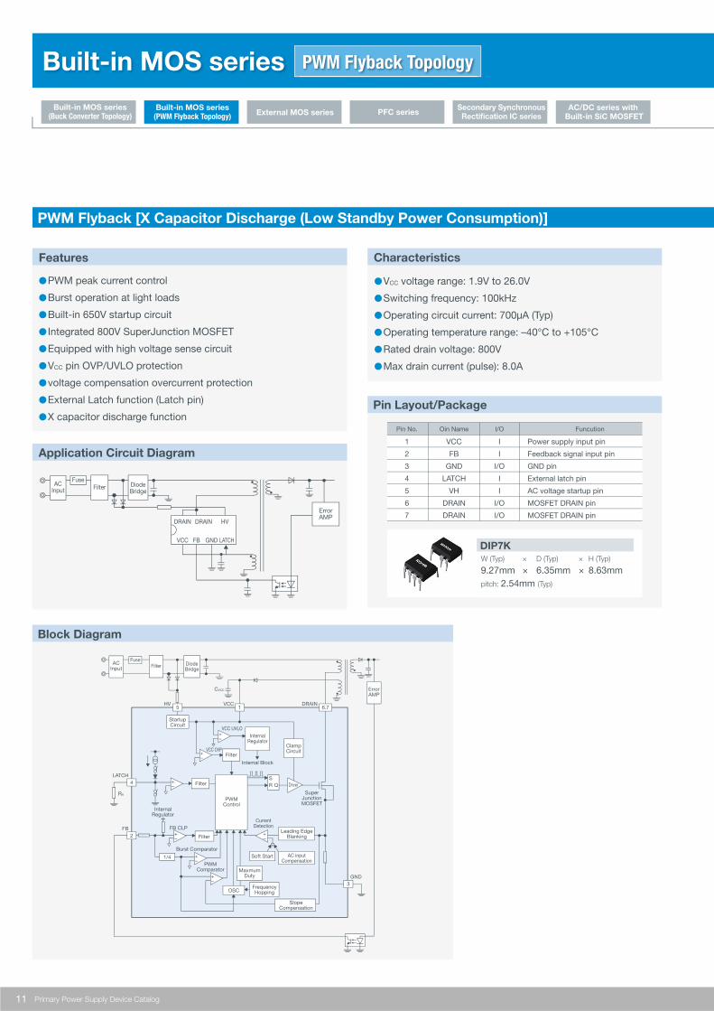
Pin No.
1
2
3
4
5
6
7
VCC
FB
GND
LATCH
VH
DRAIN
DRAIN
I
I
I/O
I
I
I/O
I/O
Power supply input pin
Feedback signal input pin
GND pin
External latch pin
AC voltage startup pin
MOSFET DRAIN pin
MOSFET DRAIN pin
Oin Name I/O Funcution
PWM Flyback [X Capacitor Discharge (Low Standby Power Consumption)]
●PWM peak current control
●Burst operation at light loads
●Built-in 650V startup circuit
● Integrated 800V SuperJunction MOSFET
●Equipped with high voltage sense circuit
●VCC pin OVP/UVLO protection
●voltage compensation overcurrent protection
●External Latch function (Latch pin)
●X capacitor discharge function
●VCC voltage range: 1.9V to 26.0V
●Switching frequency: 100kHz
●Operating circuit current: 700μA (Typ)
●Operating temperature range: –40°C to +105°C
●Rated drain voltage: 800V
●Max drain current (pulse): 8.0A
Characteristics
DIP7KW (Typ) × D (Typ) × H (Typ)
9.27mm × 6.35mm × 8.63mmpitch: 2.54mm (Typ)
Features
Application Circuit Diagram
Pin Layout/Package
Block Diagram
ACInput Filter
FuseDiodeBridge
DRAIN
VCC FB GND LATCH
DRAIN HV
ErrorAMP
ACInput Filter
HV
FuseDiodeBridge
+–
+–
+–
+–
ClampCircuit
InternalRegulator
+–
+–
ErrorAMP
+–
5VCC
VCC UVLO
VCC OVP
CVCC
1DRAIN
6.7
StartupCircuit
GND3
SuperJunctionMOSFET
DriverSR Q
Filter
Filter
Filter
InternalRegulator
Burst Comparator
PWMComparator
OSCFrequenoyHopping
PWMControl
LATCH4
FB FB CLP
2
1/4
RA
MaxmumDuty
Soft Start AC inputCompensation
Leading EdgeBlanking
CurrentDetection
Intemal Block
SlopeCompensation
Built-in MOS series(Buck Converter Topology)
Built-in MOS series(PWM Flyback Topology) External MOS series PFC series
Secondary SynchronousRectification IC series
AC/DC series with Built-in SiC MOSFET
Built-in MOS series PWM Flyback Topology
12Primary Power Supply Device Catalog
PackagePart No.
Part No.
BreakDownVoltage (V)
On resistanse(Typ) (Ω)
On resistanse(Max) (Ω)
Frequency(kHz)
FrequencyReduction
VCC OVP BR UVLO BR OVP X-Cap.Discharge Function
BM2P26CK
BM2P011
BM2P012
BM2P013
BM2P014
BM2P031
BM2P032
BM2P033
BM2P034
BM2P051
BM2P052
BM2P053
BM2P054
BM2P091
BM2P092
BM2P093
BM2P094
BM2P0141
BM2P0322
BM2P039
BM2P0391
BM2P051F
BM2P052F
BM2P053F
BM2P054F
BM2P091F
BM2P092F
BM2P093F
BM2P094F
BM2P0522F
BM2P0922F
BM2P074KF
BM2P012T
BM2P014T
DIP7K
DIP7K
DIP7K
SOP8
SOP8
TO220
SOP8
1.40
2.40
4.00
8.50
External Setting
—
External Setting
—
External Setting
—
External Setting
—
DIP7K
650
650
1.40
4.00
4.00
8.50
6.70
650 2.40
—
External Setting
Internal
Auto Restart External Setting
External Setting
External Setting
—
—
External Setting
External Setting
—
—
External Setting
—
External Setting
—
External Setting
—
External Setting
—
—
External Setting
—
External Setting
External Setting
External Setting
—
—
External Setting
External Setting
—
— —
—
—Auto Restart
4.00
8.50
650
650
650 1.40
2.00
4.00
5.40
12.00
2.00
5.40
5.40
12.00
8.50
4.00
5.40
12.00
2.00
800
650
800
65
65
65
65
65
65
100
100
65
Latch
Latch
Auto Restart
Latch
Auto Restart
Latch
Auto Restart
Latch
Auto Restart
Latch
Auto Restart
Latch
Auto Restart
Latch
Auto Restart
Latch
Auto Restart
Auto Restart
Auto Restart
Latch
Auto Restart
Latch
Auto Restart
Latch
Auto Restart
Latch
Auto Restart
Auto Restart
Auto Restart
Auto Restart
—
—
—
—
—
—
Package BreakDownVoltage (V)
On resistanse(Typ) (Ω)
On resistanse(Max) (Ω)
Frequency(kHz)
FrequencyReduction
VCC OVP BR UVLO BR OVP X-Cap.Discharge Function
BM2P016
BM2P0161
BM2P0361
BM2P015
BM2P0151
BM2PA15
BM2PA35
BM2PA55
BM2P0161K
BM2P095F
BM2PA96F
BM2P016T
1.40
1.00
3.00
1.40
1.00
1.40
2.40
8.50
1.60
—
—
—
—
—
—
—
—
—
—
—
—
—
—
DIP7K
DIP7K
SOP8
TO220
800
650
650
8.50
1.40
2.00
2.00
4.80
2.00
1.35
2.00
4.00
12.00
2.15
12.00
2.00
650
65
65
65
65
Auto Restart
Latch
Auto Restart
Latch
Auto Restart
Auto Restart
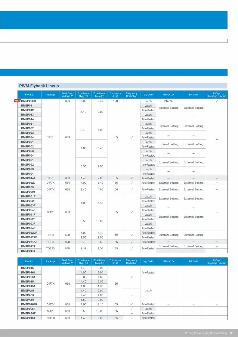
PWM Flyback Lineup
6.00 8.40
13 Primary Power Supply Device Catalog
PowerLess than
400W
Less than200W
Time
BCM Mode PFC Auxiliary Winding type
CCM Mode PFCGate ClamperBCM PFC
Resister type
650V StarterBCM Mode PFCLinear type QRX-cap DischargePFC Auto ON/OFFPFC Voltage Valuable
Linear type650V Starter Gate ClamperFsw=120kHz
Bottom skip functionLinear type650V Starter Gate ClamperFsw=110kHz
for SiC MOSFET DriveLinear typeGate ClamperFsw=120kHz (Max)
Low noise, high frequencySwitch Clamp
650V Starter Gate ClamperFsw=65kHz/120kHz
650V Starter Gate ClamperMinus Current SenseExternal Latch FunctionFsw=5kHz/100kHz/130kHz
Gate ClamperX-Cap Discharge FunctionLow Stand-by Power Function
Fsw=300kHz (Max)
PFC
PFC+QR
QR
PWM
External MOS series Features
Flyback circuit (PWM/QR) with external MOSFET. A broad lineup is offered.
■Packages: SOP-J8/SOP-J7■Output power: Up to 150W class (depending on power supply specifications)
■ Overview ■ Technology Trend
The technological trend is towards higher efficiency and lower standby power consumption. A wide range of ICs is available that incorporate a variety of functions, including those for reducing standby power consumption and transformer ringing noise.
Roadmap
14
23
ACIN_L
ACIN_IN +
+
+
+
VOUT
GND
2
1
3
4
5
1ACMONI FB CS GND
VH NC VCC OUT
2 3 4
8 7 6 5
BCM Mode PFC Resister type
BD7691FJ (SOP-J8)
BD7690FJ (SOP-J8)
BD76xxFJBD7692FJ (SOP-J8)
BM1C101/102F (SOP18)
BM1Q001/002FJ (SOP-J8) BM1Q104FJ (SOP-J8) BD768xFJ (SOP-J8) BMxFJ (SOP-J8)
BM1P061/062FJBM1P101/102FJ (SOP-J8)
BM1PxxBFJ (SOP-J7) BM1PxxCFJ (SOP-J7) BMxFJ (SOP-J8)
Applicable Products
Applications
BM1Pxxx series (PWM)
BM1Qxxx series (QR)
HomeAppliances
IndustrialEquipmentTVs
AC/DC
R65xxKNX (650V)
R80xxKNX (800V)
MOSFET
Built-in MOS series(Buck Converter Topology)
Built-in MOS series(PWM Flyback Topology) External MOS series PFC series
Secondary SynchronousRectification IC series
AC/DC series with Built-in SiC MOSFET
External MOS series
*QR: Quasi-Resonant
14Primary Power Supply Device Catalog
PackagePart No.
Part No.
Part No.
Frequency(kHz)
FrequencyReduction
FrequencyJitter VCC OVP BR UVLO FBOLP ZTOVP TSD
Burst Freq.Control
X-Cap.Discharge Function
BD7671FJ
BD7672BG
BD7673AG
BD7679G
BD7678FJ
BM1P061FJ
BM1P062FJ
BM1P065FJ
BM1P066FJ
BM1P067FJ
BM1P068FJ
BM1P101FJ
BM1P102FJ
BM1P105FJ
BM1P107FJ
BM1P10CFJ
BM1P06CFJ
—
—
—
—
Latch
Latch
Latch
AR
Latch
AR
Latch
AR
Latch
AR
Latch
AR
Latch
AR
AR
—
—
SOP-J8
SSOP6
SSOP6
SSOP6
SOP-J8
SOP-J8
SOP-J8
SOP-J7
65
65
65
65
65
65
65
100
100
65
—
—
—
—
AR
AR
Latch
AR
AR
AR—
—
—
AR Latch
AR
AR
Latch
AR
AR
—
Latch
AR
AR
AR
AR
AR
—
—
—
—
—
—
—
—
—
AR
AR
— —
—
—
—
—
—
—
Package Control method Max Frequency(kHz)
FrequencyReduction
ZTTimeout
VCC
OVPBurst Freq.
ControlBurst Freq.
ControlGain
change2stage Timeout
BD7681FJ
BM1Q001FJ
BM1Q002FJ
BM1Q011FJ
BM1Q021FJ
BM1Q103FJ
BM1Q104FJ
120
120 —
120
116
15μs AR
15μs
15μs —
—
—15μs —
Latch
AR
Latch
AR
AR
BR UVLO
AR
AR
AR
Latch
—
Latch
—
AR
Latch
FBOLP ZTOVP
SOP-J8
SOP-J8
SOP-J8
SOP-J7
SOP-J8
Max frequency
Max frequency
Max frequency
Bottom Skip
—
—
—
—
—
—
—
—
—
—
—
Package QR Controlmethod
Max Frequency(kHz)
QR FrequencyReduction
PFC Controlmethod
PFC MaxFrequency
PFC frequencyjitter
VCC OVP
BD7690FJ
BD7691FJ
BD7692FJ
BM1050AF
BM1051F
BM1C101F
BM1C102F
120
—
—
—
—
—
—
BCM
BCM
BCM
—
—
—
—
—
—
—
—
—
—
—
—
—
—
—
65kHzFixed
220kHz
220kHz
400kHz
500kHzVoltagemode
Peakcurrent
120
Latch/AR
Latch
QR FBOLP
AR
AR
PFC VoltageSwitch
X-cap.Discharge
— —
—
SOP24
SOP-J8
SOP-J8
SOP-J8
SOP18
Max frequency
—
—
—
Max frequency
—
External MOS series Lineup
PWM
QR (Pseudo-Resonant)
AC/DC+PFC
15 Primary Power Supply Device Catalog
BD7692FJBCM ZCD Resistance detection
CCM PFC IC(Under Development)
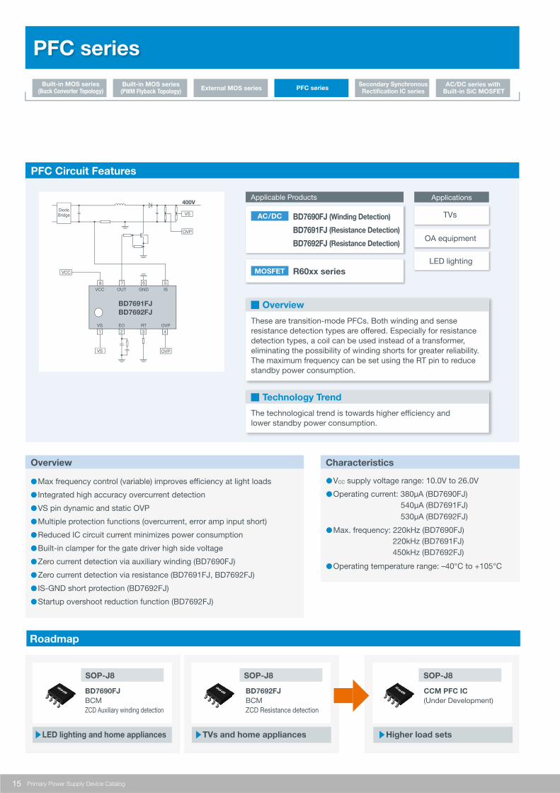
●Max frequency control (variable) improves efficiency at light loads
● Integrated high accuracy overcurrent detection
●VS pin dynamic and static OVP
●Multiple protection functions (overcurrent, error amp input short)
●Reduced IC circuit current minimizes power consumption
●Built-in clamper for the gate driver high side voltage
●Zero current detection via auxiliary winding (BD7690FJ)
●Zero current detection via resistance (BD7691FJ, BD7692FJ)
● IS-GND short protection (BD7692FJ)
●Startup overshoot reduction function (BD7692FJ)
▶LED lighting and home appliances
SOP-J8 SOP-J8 SOP-J8
1 2
8 7 6 5
3 4
DiodeBridge
400V
VS
OVP
VCC OUT GND IS
VS
VS
EO RT OVP
OVP
VCC
BD7691FJBD7692FJ
●VCC supply voltage range: 10.0V to 26.0V
●Operating current: 380μA (BD7690FJ) 540μA (BD7691FJ)
530μA (BD7692FJ)
●Max. frequency: 220kHz (BD7690FJ) 220kHz (BD7691FJ) 450kHz (BD7692FJ)
●Operating temperature range: –40°C to +105°C
CharacteristicsOverview
Roadmap
PFC Circuit Features
■ Overview
■ Technology Trend
The technological trend is towards higher efficiency and lower standby power consumption.
These are transition-mode PFCs. Both winding and sense resistance detection types are offered. Especially for resistance detection types, a coil can be used instead of a transformer, eliminating the possibility of winding shorts for greater reliability. The maximum frequency can be set using the RT pin to reduce standby power consumption.
BD7690FJBCMZCD Auxiliary winding detection
▶TVs and home appliances ▶Higher load sets
TVs
LED lighting
OA equipment
ApplicationsApplicable Products
BD7690FJ (Winding Detection)
BD7691FJ (Resistance Detection)
BD7692FJ (Resistance Detection)
AC/DC
R60xx series MOSFET
Built-in MOS series(Buck Converter Topology)
Built-in MOS series(PWM Flyback Topology) External MOS series PFC series
Secondary SynchronousRectification IC series
AC/DC series with Built-in SiC MOSFET
PFC series
16Primary Power Supply Device Catalog
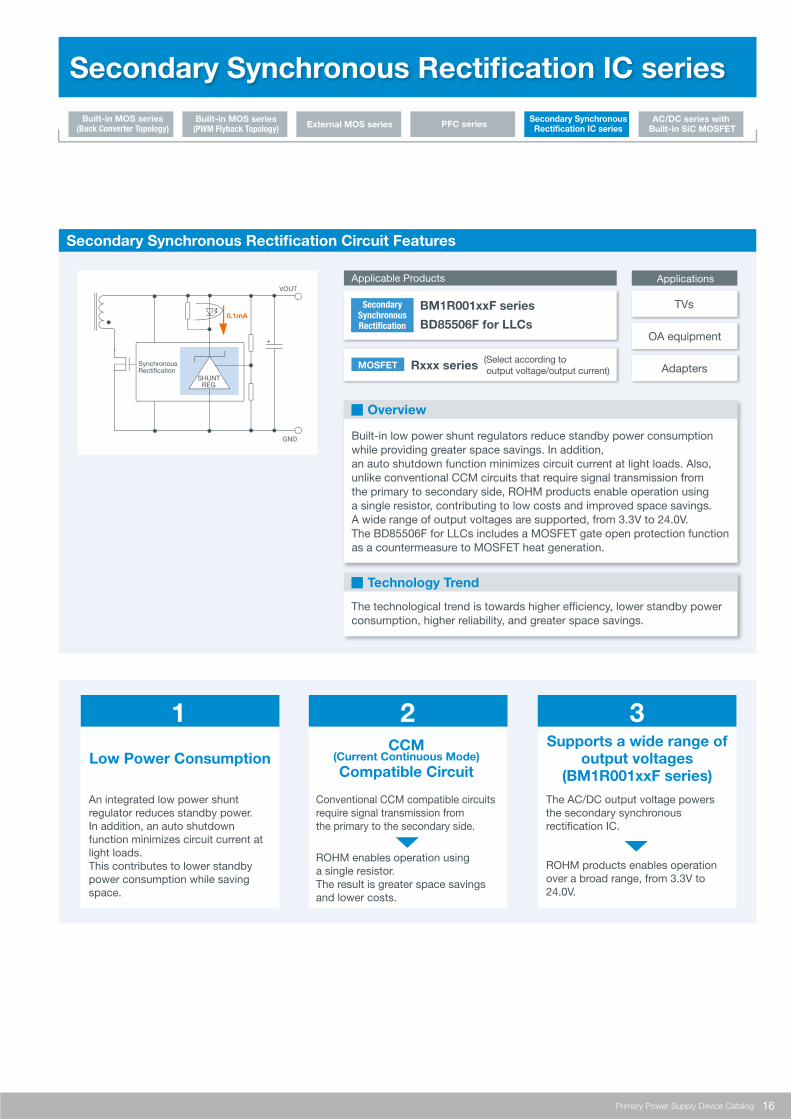
Low Power Consumption
An integrated low power shunt regulator reduces standby power. In addition, an auto shutdown function minimizes circuit current at light loads. This contributes to lower standby power consumption while saving space.
Conventional CCM compatible circuits require signal transmission from the primary to the secondary side.
ROHM enables operation using a single resistor. The result is greater space savings and lower costs.
The AC/DC output voltage powers the secondary synchronous rectification IC.
ROHM products enables operation over a broad range, from 3.3V to 24.0V.
CCM(Current Continuous Mode)Compatible Circuit
Supports a wide range ofoutput voltages
(BM1R001xxF series)
+
SynchronousRectification
VOUT
GND
SHUNTREG
0.1mA
Secondary Synchronous Rectification Circuit Features
■ Overview
■ Technology Trend
The technological trend is towards higher efficiency, lower standby power consumption, higher reliability, and greater space savings.
Built-in low power shunt regulators reduce standby power consumption while providing greater space savings. In addition, an auto shutdown function minimizes circuit current at light loads. Also, unlike conventional CCM circuits that require signal transmission from the primary to secondary side, ROHM products enable operation using a single resistor, contributing to low costs and improved space savings. A wide range of output voltages are supported, from 3.3V to 24.0V. The BD85506F for LLCs includes a MOSFET gate open protection function as a countermeasure to MOSFET heat generation.
1 2 3
TVs
Adapters
OA equipment
ApplicationsApplicable Products
BM1R001xxF series
BD85506F for LLCs
SecondarySynchronousRectification
Rxxx series MOSFET(Select according to output voltage/output current)
Built-in MOS series(Buck Converter Topology)
Built-in MOS series(PWM Flyback Topology) External MOS series PFC series
Secondary SynchronousRectification IC series
AC/DC series with Built-in SiC MOSFET
Secondary Synchronous Rectification IC series
17 Primary Power Supply Device Catalog
Supply Voltage Range(V) (Max)Part No.
Normal Operating Current(μA) (Typ)
BM2SCQ121T-LB
BM2SCQ122T-LB
BM2SCQ123T-LB
BM2SCQ124T-LB
VCC: 15.0 to 27.5DRAIN: 1,700
2,000
Burst Operating Current(μA) (Typ)
500
Max Operating Frequency(kHz) (Typ)
120
FB OLP
Auto Restart
Latch
Auto Restart
Latch
VCC OVP
Latch
Latch
Auto Restart
Auto Restart
Operating Temperature(°C)
–40 to +105
0 10 20 30
Output Power (W)P
ower
Con
vers
ion
Eff
ecie
ncy
(%)
40 50 60 70 80
75
80
85
90
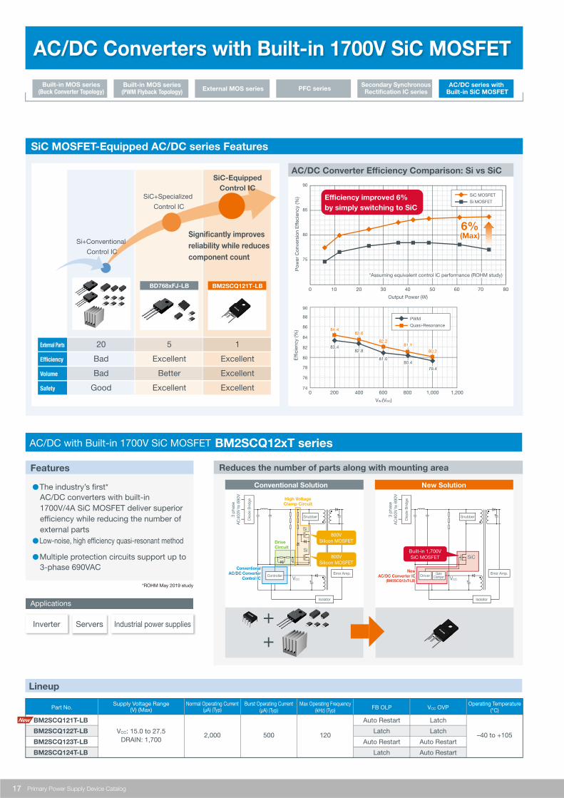
Significantly improvesreliability while reducescomponent count
External Parts
Efficiency
Volume
Safety
20
Bad
Bad
Good
5
Excellent
Better
Excellent
1
Excellent
Excellent
Excellent0 200 400 600
VIN (VDC)
Effi
cien
cy (%
)
800 1,000 1,20074
76
78
80
82
84
86
90
88
84.484.4
83.483.4
83.683.6
82.882.8
82.282.2
81.081.0
81.181.1
80.480.4
80.280.2
79.479.4
PWM
Quasi-Resonance
6%(Max)6%(Max)
SiC MOSFET
Si MOSFET
●The industry’s first*AC/DC converters with built-in 1700V/4A SiC MOSFET deliver superior efficiency while reducing the number of external parts
●Low-noise, high efficiency quasi-resonant method
●Multiple protection circuits support up to 3-phase 690VAC
Features
Lineup
AC/DC with Built-in 1700V SiC MOSFET BM2SCQ12xT series
SiC MOSFET-Equipped AC/DC series Features
Inverter Industrial power suppliesServers
Conventional Solution New Solution
++
SiC+Specialized
Control IC
SiC-EquippedControl IC
BD768xFJ-LB BM2SCQ121T-LB
*Assuming equivalent control IC performance (ROHM study)*Assuming equivalent control IC performance (ROHM study)
AC/DC Converter Efficiency Comparison: Si vs SiC
Reduces the number of parts along with mounting area
Applications
Efficiency improved 6% by simply switching to SiC
*ROHM May 2019 study
SiC
VCC
NewAC/DC Converter IC
(BM2SCQ12xT-LB)
NewAC/DC Converter IC
(BM2SCQ12xT-LB)
Isolator
Error Amp.
3 p
hase
AC
400V
to 6
90V
Dio
de
Brid
ge
Driver GateClamper
Built-in 1,700VSiC MOSFET
Snubber
Si
Snubber
Si
VCCController
ConventionalAC/DC Converter
Control IC
ConventionalAC/DC Converter
Control IC
High VoltageClamp Circuit
Isolator
Error Amp.
800VSilicon MOSFET
3 p
hase
AC
400V
to 6
90V
Dio
de
Brid
ge
800VSilicon MOSFET
DriveCircuitDriveCircuit
Built-in MOS series(Buck Converter Topology)
Built-in MOS series(PWM Flyback Topology) External MOS series PFC series
Secondary SynchronousRectification IC series
AC/DC series with Built-in SiC MOSFET
AC/DC Converters with Built-in 1700V SiC MOSFET
Si+Conventional
Control IC
18Primary Power Supply Device Catalog
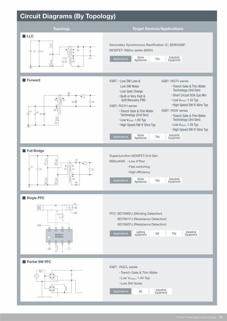
■ LLC
■ Forward
■ Full Bridge
■ Single PFC
■ Partial SW PFC
Secondary Synchronous Rectification IC: BD85506F
MOSFET: R60xx series (600V)
SuperJunction MOSFET-2nd Gen
R60xxKNX ・Low A*Ron
・Fast switching
・High efficiency
IGBT: ・Low SW Loss &
Low SW Noise
・Low Gate Charge ・Built-in Very Fast & Soft Recovery FRD
IGBT: RGTH series
・Trench Gate & Thin Wafer Technology (2nd Gen)
・Low VCE(sat.) 1.6V Typ ・High Speed SW tf 50ns Typ
PFC: BD7690FJ (Winding Detection)
BD7691FJ (Resistance Detection)
BD7692FJ (Resistance Detection)
IGBT: RGCL series
・Trench Gate & Thin Wafer
・Low VCE(sat.) 1.4V Typ
・Low SW Noise
Circuit Diagrams (By Topology)
Topology Target Devices/Applications
V1 C1
Q1
P1
TR
S1D1
C3
C2
Q2
S2
V1 C1
P1
TRD2
D3 C2
L1S1
P2
Q1
D1
V1C1
Q1
Q2
Q3
Q4
P1
TR
D1
S1
S2
D2
C2
L1
PS1
Applications
IGBT: RGTV series
・Trench Gate & Thin Wafer Technology (3rd Gen)
・Short Circuit SOA 2μs Min ・Low VCE(sat.) 1.5V Typ ・High Speed SW tf 40ns Typ
IGBT: RGW series
・Trench Gate & Thin Wafer Technology (3rd Gen)
・Low VCE(sat.) 1.5V Typ ・High Speed SW tf 30ns Typ
HomeAppliances TVs Industrial
Equipment
Applications HomeAppliances TVs Industrial
Equipment
Applications HomeAppliances TVs Industrial
Equipment
Applications Lightingequipment TVsOA Industrial
Equipment
Applications IndustrialEquipmentAC
1 2
8 7 6 5
3 4
Dio
deB
ridge
400V
VS
OVP
VCC
VS
VCC OUT GND IS
VS EO
BD7691FJBD7692FJ
RT OVP

19 Primary Power Supply Device Catalog
■ Interleaved PFC
■ Totem-Pole Di Bridgeless PFC
■ Totem-Pole Di Bridgeless PFC(Synchronous Rectification)
IGBT: ・Low SW Loss & Low SW Noise
・Low Gate Charge
・Built-in Very Fast & Soft Recovery FRD
IGBT: RGTH series
・Trench Gate & Thin Wafer Technology (2nd Gen)
・Low VCE(sat.) 1.6V Typ
・High Speed SW tf 50ns Typ
IGBT: RGTV series
・Trench Gate & Thin Wafer Technology (3rd Gen)
・Short Circuit SOA 2μs Min
・Low VCE(sat.) 1.5V Typ
・High Speed SW tf 40ns Typ
IGBT: RGW series
・Trench Gate & Thin Wafer Technology (3rd Gen)
・Low VCE(sat.) 1.5V Typ
・High Speed SW tf 30ns Typ
Switching Side
IGBT: RGT series
・Trench Gate & Thin Wafer Technology (2nd Gen)
・Short Circuit SOA 5μs Min
・Low VCE(sat) 1.65V Typ
・High Speed SW
・Low SW Loss & Low SW Noise
・Low Gate Charge
・Built-in Very Fast & Soft Recovery FRD
Switching Side
Presto MOS: R60xxJNx series
Fast- Recovery Body Diode SuperJunction MOSFET
Presto MOS 2nd gen. R60xxMNx
・Fast trr/Low Rds(on)
・Improvement for Efficiency about Motors.
・Able to remove parallel diode
Rectification Side
SJ-MOS: Low Noise SuperJunction MOSFET
2nd Gen R60xxENx
Circuit Diagrams (By Topology)
Topology Target Devices/Applications
PS1
PS1
PS1
PS1
High Efficiency+Low Noise
Light Load High Efficiency
Light Load High Efficiency
ACApplications
Applications
Applications
Applications
IndustrialEquipment
HomeAppliances TVs Industrial
Equipment
HomeAppliances TVs Industrial
Equipment
HomeAppliances TVs Industrial
Equipment

20Primary Power Supply Device Catalog
Higher efficiency
2017 2018 2019 or more
●Low loss: switching=20mW
●12V FET drive voltage control (reduces FED drive switching loss)
High reliability●Multiple protection functions (OVP, VCC UVLO, OUT short, IS short )
● Integrated external FET protection (12V CLAMP)-eliminates the need for Zener diode for FET protection
Reduced development load ● Industry-standard pin layout allows the board to be evaluated as-is
PFC (Power Factor Correction) ICs
Application Support
SOP-J8BD7691FJBCMZCD is detected by resister
MP
SOP-J8BD7692FJBCM (resister)BD7691FJ+more protection
Higher reliability and lower noise
MP
SOP-J8BD76xxFJCCMSOP-J8
BD7690FJBCMZCD is detected by auxiliary winding
MP
3TInsulation tape
NP1 NP2NS1 NS2 NS3ND
1T
ROHM provides various application support tools and welcomes customer requests regarding the power supply block circuit.
Schematics Transformer Specifications Characteristics Evaluation(Comparison)
Noise CharacteristicsEvaluation Heat Generation Evaluation Consultation of Board Layout
We also promote further development of the customer’s power supply block through technical support utilizing actual equipment (including ICs and discretes) together with simulations.
Circuit Evaluation・efficiency Noise Evaluation
Trans Design Application Evaluation Layout
ROHM proposes and develop products with the following features
Noise Terminal Voltage
M
M
M
21 Primary Power Supply Device Catalog
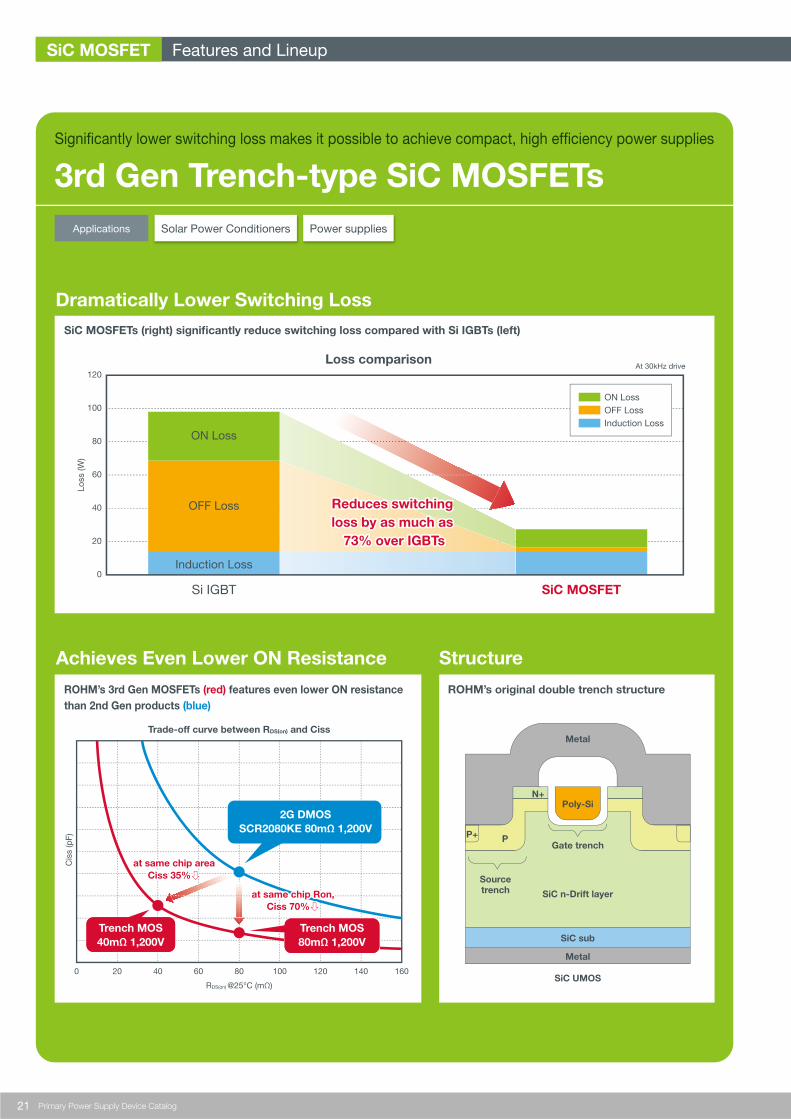
3rd Gen Trench-type SiC MOSFETs
SiC MOSFETs (right) significantly reduce switching loss compared with Si IGBTs (left)
ROHM’s 3rd Gen MOSFETs (red) features even lower ON resistance than 2nd Gen products (blue)
ROHM’s original double trench structure
Loss comparison
Si IGBT SiC MOSFET
Induction Loss
OFF Loss
ON Loss
At 30kHz drive
0
20
40
60
80
100
120
Loss
(W)
Reduces switching loss by as much as
73% over IGBTs
Reduces switching loss by as much as
73% over IGBTs
ON LossOFF LossInduction Loss
160140120100806040200
Trade-off curve between RDS(on) and Ciss
Cis
s (p
F)
RDS(on) @25°C (mΩ)
at same chip areaCiss 35%⇩
at same chip areaCiss 35%⇩
at same chip Ron,Ciss 70%⇩
at same chip Ron,Ciss 70%⇩
Trench MOS40mΩ 1,200V
Trench MOS80mΩ 1,200V
2G DMOSSCR2080KE 80mΩ 1,200V
Metal
Metal
Gate trenchP+
N+
P
Sourcetrench SiC n-Drift layer
SiC sub
SiC UMOS
Poly-Si
Dramatically Lower Switching Loss
SiC MOSFET Features and Lineup
Achieves Even Lower ON Resistance Structure
Applications Solar Power Conditioners Power supplies
Significantly lower switching loss makes it possible to achieve compact, high efficiency power supplies
22Primary Power Supply Device Catalog
2nd Gen (Planar type)
3rd Gen (Trench type)
Part No.Polarity
(ch)VDSS
(V)ID(A)
PD (W)(TC=25°C)
RDS (on)
(Typ) (mΩ)
Qg(Typ) (nC)
Drive Voltage(V)VGS=18V
PackageAutomotive Grade
(AEC-Q101 Qualified)
SCT2120AF
SCH2080KE
SCT2080KE
SCT2160KE
SCT2280KE
SCT2450KE
SCT2750NY
SCT2H12NY
SCT2H12NZ
N
N
N
N
N
N
N
N
N
650
1,200
1,200
1,200
1,200
1,200
1,700
1,700
1,700
29
40
40
22
14
10
5.9
4
3.7
165
262
262
165
108
85
57
44
35
120
80
80
160
280
450
750
1,150
1,150
61
106
106
62
35
27
17
14
14
18
18
18
18
18
18
18
18
18
TO-220AB
TO-247
TO-268-2L
TO-3PFM
—
—
YES
—
—
—
—
—
—
SCT3017AL
SCT3022AL
SCT3030AL
SCT3060AL
SCT3080AL
SCT3120AL
SCT3022KL
SCT3030KL
SCT3040KL
SCT3080KL
SCT3105KL
SCT3160KL
N
N
N
N
N
N
N
N
N
N
N
N
650
650
650
650
650
650
1,200
1,200
1,200
1,200
1,200
1,200
118
93
70
39
30
21
95
72
55
31
24
17
427
339
262
165
134
103
427
339
262
165
134
103
17
22
30
60
80
120
22
30
40
80
105
160
172
133
104
58
48
38
178
131
107
60
51
42
18
18
18
18
18
18
18
18
18
18
18
18
TO-247(TO-247N)
YES
YES
YES
YES
YES
YES
YES
YES
YES
YES
YES
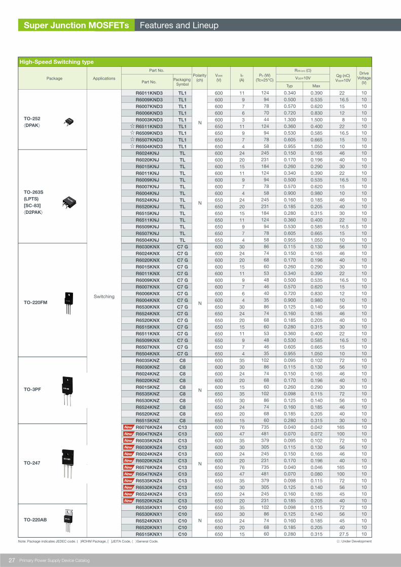
YESNote: Package indicates JEDEC code. ( ) denotes ROHM package type.
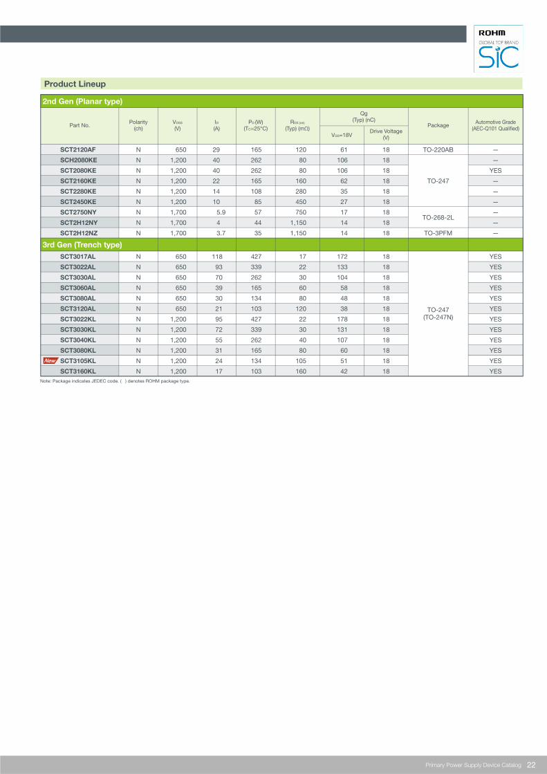
Product Lineup
23 Primary Power Supply Device Catalog
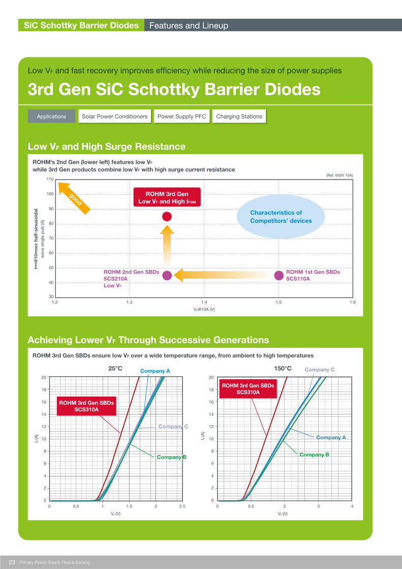
3rd Gen SiC Schottky Barrier DiodesLow VF and fast recovery improves efficiency while reducing the size of power supplies
ROHM’s 2nd Gen (lower left) features low VF while 3rd Gen products combine low VF with high surge current resistance
ROHM 3rd Gen SBDs ensure low VF over a wide temperature range, from ambient to high temperatures
1.3 1.4 1.5 1.61.230
40
50
60
70
80
90
100
110
IFM
S@
10m
sec
half-
sinu
soid
alw
ave
sing
le p
uls
(A)
ROHM 3rd GenLow VF and High IFSM
good
(Ref. 650V 10A)
VF@10A (V)
Characteristics of Competitors’ devices
ROHM 1st Gen SBDsSCS110AROHM 1st Gen SBDsSCS110A
ROHM 2nd Gen SBDsSCS210ALow VF
ROHM 2nd Gen SBDsSCS210ALow VF
ROHM 3rd Gen SBDsSCS310A
25°C
00 0.5 1 1.5 2 2.5
2
4
6
8
10
12
14
16
18
20
I F (A
)
VF (V)
I F (A
)
150°C
00 0.5 2 3 4
2
4
6
8
10
12
14
16
18
20
VF (V)
Compompany By B Company B
SiC Schottky Barrier Diodes
Low VF and High Surge Resistance
Achieving Lower VF Through Successive Generations
Compompany A ACompany A
Compompany C CCompany C
Compompany By B Company B
Compompany A ACompany A
Compompany C CCompany C
Features and Lineup
Applications Solar Power Conditioners Power Supply PFC Charging Stations
ROHM 3rd Gen SBDsSCS310A
24Primary Power Supply Device Catalog
SiC Schottky Barrier Diodes
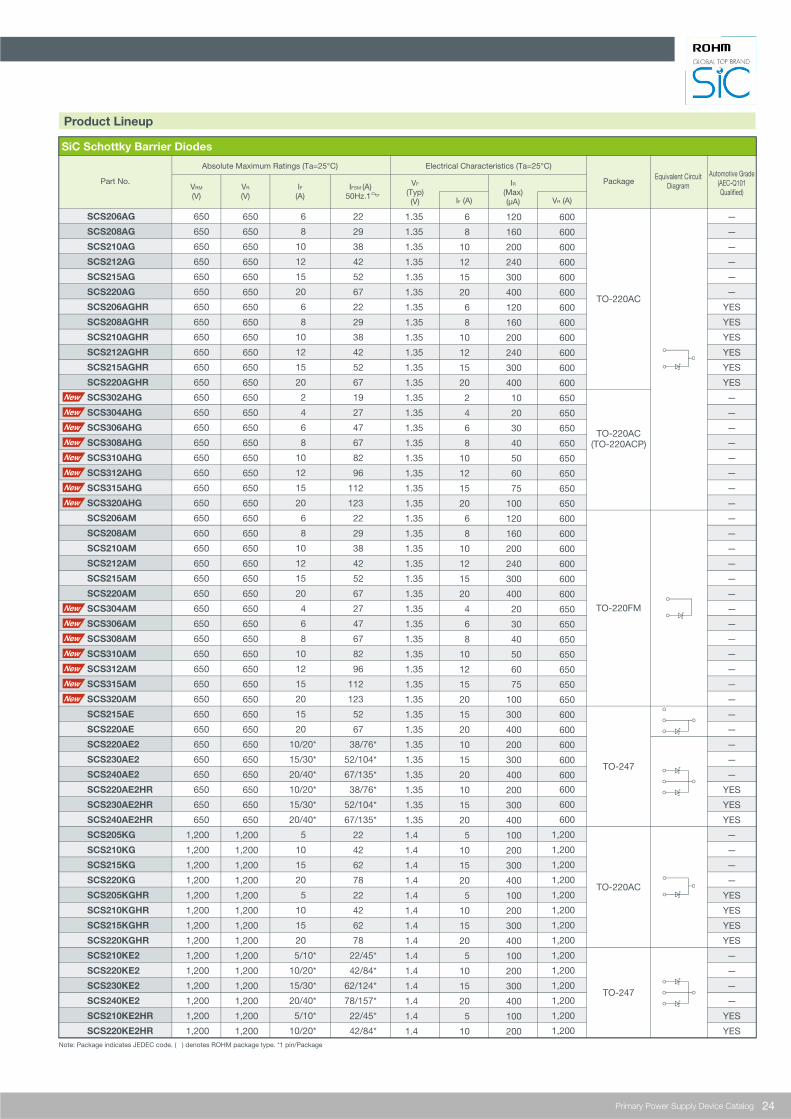
Product Lineup
Part No.
Absolute Maximum Ratings (Ta=25°C) Electrical Characteristics (Ta=25°C)
VRM
(V)VR
(V)IF
(A) IF (A)
VF
(Typ)(V) VR (A)
IR(Max)(μA)
PackageEquivalent Circuit
Diagram
Automotive Grade(AEC-Q101Qualified)
SCS206 AG
SCS208AG
SCS210AG
SCS212AG
SCS215AG
SCS220AG
SCS206 AGHR
SCS208AGHR
SCS210AGHR
SCS212AGHR
SCS215AGHR
SCS220AGHR
SCS302AHG
SCS304 AHG
SCS306 AHG
SCS308AHG
SCS310AHG
SCS312AHG
SCS315AHG
SCS320AHG
SCS206 AM
SCS208AM
SCS210AM
SCS212AM
SCS215AM
SCS220AM
SCS304 AM
SCS306 AM
SCS308AM
SCS310AM
SCS312AM
SCS315AM
SCS320AM
SCS215AE
SCS220AE
SCS220AE2
SCS230AE2
SCS24 0AE2
SCS220AE2HR
SCS230AE2HR
SCS24 0AE2HR
SCS205KG
SCS210KG
SCS215KG
SCS220KG
SCS205KGHR
SCS210KGHR
SCS215KGHR
SCS220KGHR
SCS210KE2
SCS220KE2
SCS230KE2
SCS24 0KE2
SCS210KE2HR
SCS220KE2HR
650
650
650
650
650
650
650
650
650
650
650
650
650
650
650
650
650
650
650
650
650
650
650
650
650
650
650
650
650
650
650
650
650
650
650
650
650
650
650
650
650
1,200
1,200
1,200
1,200
1,200
1,200
1,200
1,200
1,200
1,200
1,200
1,200
1,200
1,200
650
650
650
650
650
650
650
650
650
650
650
650
650
650
650
650
650
650
650
650
650
650
650
650
650
650
650
650
650
650
650
650
650
650
650
650
650
650
650
650
650
1,200
1,200
1,200
1,200
1,200
1,200
1,200
1,200
1,200
1,200
1,200
1,200
1,200
1,200
1.35
1.35
1.35
1.35
1.35
1.35
1.35
1.35
1.35
1.35
1.35
1.35
1.35
1.35
1.35
1.35
1.35
1.35
1.35
1.35
1.35
1.35
1.35
1.35
1.35
1.35
1.35
1.35
1.35
1.35
1.35
1.35
1.35
1.35
1.35
1.35
1.35
1.35
1.35
1.35
1.35
1.4
1.4
1.4
1.4
1.4
1.4
1.4
1.4
1.4
1.4
1.4
1.4
1.4
1.4
6
8
10
12
15
20
6
8
10
12
15
20
2
4
6
8
10
12
15
20
6
8
10
12
15
20
4
6
8
10
12
15
20
15
20
10
15
20
10
15
20
5
10
15
20
5
10
15
20
5
10
15
20
5
10
120
160
200
240
300
400
120
160
200
240
300
400
10
20
30
40
50
60
75
100
120
160
200
240
300
400
20
30
40
50
60
75
100
300
400
200
300
400
200
300
400
100
200
300
400
100
200
300
400
100
200
300
400
100
200
600
600
600
600
600
600
600
600
600
600
600
600
650
650
650
650
650
650
650
650
600
600
600
600
600
600
650
650
650
650
650
650
650
600
600
600
600
600
600
600
600
1,200
1,200
1,200
1,200
1,200
1,200
1,200
1,200
1,200
1,200
1,200
1,200
1,200
1,200
6
8
10
12
15
20
6
8
10
12
15
20
2
4
6
8
10
12
15
20
6
8
10
12
15
20
4
6
8
10
12
15
20
15
20
10/20*
15/30*
20/40*
10/20*
15/30*
20/40*
5
10
15
20
5
10
15
20
5/10*
10/20*
15/30*
20/40*
5/10*
10/20*
22
29
38
42
52
67
22
29
38
42
52
67
19
27
47
67
82
96
112
123
22
29
38
42
52
67
27
47
67
82
96
112
123
52
67
38/76*
52/104*
67/135*
38/76*
52/104*
67/135*
22
42
62
78
22
42
62
78
22/45*
42/84*
62/124*
78/157*
22/45*
42/84*
TO-220AC
TO-220FM
TO-247
TO-220AC
TO-247
TO-220AC(TO-220ACP)
—
—
—
—
—
—
YES
YES
YES
YES
YES
YES
—
—
—
—
—
—
—
—
—
—
—
—
—
—
—
—
—
—
—
—
—
—
—
—
—
—
YES
YES
YES
—
—
—
—
YES
YES
YES
YES
—
—
—
—
YES
YES
IFSM (A)50Hz.1
Note: Package indicates JEDEC code. ( ) denotes ROHM package type. *1 pin/Package
25 Primary Power Supply Device Catalog
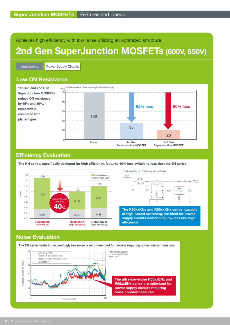
1st Gen and 2nd Gen
SuperJunction MOSFETs
reduce ON resistance
by 65% and 80%,
respectively,
compared with
planar types
The KN series, specifically designed for high efficiency, features 40% less switching loss than the EN series
The EN series featuring exceedingly low noise is recommended for circuits requiring noise countermeasures
Planar 1st GenSuperJunction MOSFET
2nd GenSuperJunction MOSFET
100
80
(%)
60
40
20
0
80% less65% less
ON-Resistance Comparison (TO-220 Package)
100
35
20
Evaluation Circuit: PFC Circuit Critical Mode
IC
Input100V/60Hz
Output120W
0.00
0.20
0.40
0.60
0.80
1.00
1.20
1.40
1.60
R6020ENX(Low Noise)
R6020KNX(High Efficiency)
Company B(High Efficiency)
Loss
(W)
0.34 0.380.36
1.14
1.501.50
0.680.82
1.02
1.20
40%
Switching loss reduced
The R60xxKNx and R65xxKNx series, capable of high-speed switching, are ideal for power supply circuits demanding low loss and high efficiency
Limit (Quasi Peak)
R6020ENX (Low Noise Type)
R6020KNX (High Efficiency Type)
Competitor A
Frequency (MHz)
Rad
iate
d E
mis
sion
(H) (
dB
μV)
30030
0
10
20
30
40
50
60 RADIATED EMISSION H (dBμV/m) 100V/60Hz Input 146W
Switching LossConduction Loss
Super Junction MOSFETs
2nd Gen SuperJunction MOSFETs (600V, 650V)
Achieves high efficiency with low noise utilizing an optimized structure
Low ON Resistance
Efficiency Evaluation
The ultra-low-noise R60xxENx and R65xxENx series are optimized for power supply circuits requiring noise countermeasures.
Features and Lineup
Applications Power Supply Circuits
Noise Evaluation

26Primary Power Supply Device Catalog
Low Noise type
Package ApplicationsPD (W)
(Tc=25°C)
RDS (on) (Ω)
VGS=10V
Typ Max
Qg (nC)VGS=10V
DriveVoltage
(V)
R6011END3R6009END3R6007END3R6004END3R6002END3R6511END3R6509END3R6507END3R6504END3R6502END3R6024ENJR6020ENJR6015ENJR6011ENJR6009ENJR6007ENJR6004ENJR6524ENJR6520ENJR6515ENJR6511ENJR6509ENJR6507ENJR6504ENJR6030ENXR6024ENXR6020ENXR6015ENXR6011ENXR6009ENXR6007ENXR6004ENXR6530ENXR6524ENXR6520ENXR6515ENXR6511ENXR6509ENXR6507ENXR6504ENXR6035ENZR6030ENZR6024ENZR6020ENZR6015ENZR6535ENZR6530ENZR6524ENZR6520ENZR6515ENZR6076ENZ4R6047ENZ4R6035ENZ4R6030ENZ4R6024ENZ4R6020ENZ4R6576ENZ4R6547ENZ4R6535ENZ4R6530ENZ4R6524ENZ4R6520ENZ4
☆☆☆☆
0.390 0.535 0.620 0.980 3.400 0.400 0.585 0.665 1.050 3.300 0.165 0.196 0.290 0.390 0.535 0.620 0.980 0.185 0.205 0.315 0.400 0.585 0.665 1.050 0.130 0.165 0.196 0.290 0.390 0.535 0.620 0.980 0.140 0.185 0.205 0.315 0.400 0.585 0.665 1.050 0.102 0.130 0.165 0.196 0.290 0.115 0.140 0.185 0.205 0.315 0.042 0.072 0.102 0.130 0.165 0.196 0.046 0.080 0.115 0.140 0.185 0.205
0.340 0.500 0.570 0.900 2.800 0.360 0.530 0.605 0.955 3.000 0.150 0.170 0.260 0.340 0.500 0.570 0.900 0.160 0.185 0.280 0.360 0.530 0.605 0.955 0.115 0.150 0.170 0.260 0.340 0.500 0.570 0.900 0.125 0.160 0.185 0.280 0.360 0.530 0.605 0.955 0.095 0.115 0.150 0.170 0.260 0.098 0.125 0.160 0.185 0.280 0.038 0.066 0.095 0.115 0.150 0.170 0.040 0.070 0.098 0.125 0.160 0.185
12494785926
12494785924
245231184124947858
24523118412494785886746860534846358674686053484635
10286746860
10286746860
735481379305245231735481379305245231
ID(A)
119741.7
119741.7
24201511974
24201511974
3024201511974
3024201511974
35302420153530242015764735302420764735302420
VDSS
(V)
600600600600600650650650650650600600600600600600600650650650650650650650600600600600600600600600650650650650650650650650600600600600600650650650650650600600600600600600650650650650650650
Polarity(ch)
Part No.
Part No. Packaging Symbol
N
N
N
N
N
TL1TL1TL1TL1TL1TL1TL1TL1TL1TL1TLTLTLTLTLTLTLTLTLTLTLTLTLTL
C7 GC7 GC7 GC7 GC7 GC7 GC7 GC7 GC7 GC7 GC7 GC7 GC7 GC7 GC7 GC7 GC8C8C8C8C8C8C8C8C8C8
C13C13C13C13C13C13C13C13C13C13C13C13
Switching
TO-252⟨DPAK⟩
TO-263S(LPTS)[SC-83]⟨D2PAK⟩
TO-220FM
TO-3PF
TO-247
32232015
6.532242015
6.5706040322320157061403224201585706040322320159070614032242015
11085706040
11390706140
260145110
857060
260145110
857060
1010101010101010101010101010101010101010101010101010101010101010101010101010101010101010101010101010101010101010101010101010
☆: Under DevelopmentNote: Package indicates JEDEC code. ( )ROHM Package, [ ]JEITA Code, ⟨ ⟩General Code.
Product Lineup
27 Primary Power Supply Device Catalog
Package ApplicationsPD (W)
(Tc=25°C)
RDS (on) (Ω)
VGS=10V
Typ Max
Qg (nC)VGS=10V
DriveVoltage
(V)
R6011KND3R6009KND3R6007KND3R6006KND3R6003KND3R6511KND3R6509KND3R6507KND3R6504KND3R6024KNJR6020KNJR6015KNJR6011KNJR6009KNJR6007KNJR6004KNJR6524KNJR6520KNJR6515KNJR6511KNJR6509KNJR6507KNJR6504KNJR6030KNXR6024KNXR6020KNXR6015KNXR6011KNXR6009KNXR6007KNXR6006KNXR6004KNXR6530KNXR6524KNXR6520KNXR6515KNXR6511KNXR6509KNXR6507KNXR6504KNXR6035KNZR6030KNZR6024KNZR6020KNZR6015KNZR6535KNZR6530KNZR6524KNZR6520KNZR6515KNZR6076KNZ4R6047KNZ4R6035KNZ4R6030KNZ4R6024KNZ4R6020KNZ4R6576KNZ4R6547KNZ4R6535KNZ4R6530KNZ4R6524KNZ4R6520KNZ4R6535KNX1R6530KNX1R6524KNX1R6520KNX1R6515KNX1
☆☆☆☆
0.390 0.535 0.620 0.830 1.500 0.400 0.585 0.665 1.050 0.165 0.196 0.290 0.390 0.535 0.620 0.980 0.185 0.205 0.315 0.400 0.585 0.665 1.050 0.130 0.165 0.196 0.290 0.390 0.535 0.620 0.830 0.980 0.140 0.185 0.205 0.315 0.400 0.585 0.665 1.050 0.102 0.130 0.165 0.196 0.290 0.115 0.140 0.185 0.205 0.315 0.042 0.072 0.102 0.130 0.165 0.196 0.046 0.080 0.115 0.140 0.185 0.205 0.115 0.140 0.185 0.205 0.315
0.340 0.500 0.570 0.720 1.300 0.360 0.530 0.605 0.955 0.150 0.170 0.260 0.340 0.500 0.570 0.900 0.160 0.185 0.280 0.360 0.530 0.605 0.955 0.115 0.150 0.170 0.260 0.340 0.500 0.570 0.720 0.900 0.125 0.160 0.185 0.280 0.360 0.530 0.605 0.955 0.095 0.115 0.150 0.170 0.260 0.098 0.125 0.160 0.185 0.280 0.040 0.070 0.095 0.115 0.150 0.170 0.040 0.070 0.098 0.125 0.160 0.185 0.098 0.125 0.160 0.185 0.280
12494787044
124947858
245231184124947858
2452311841249478588674686053484640358674686053484635
10286746860
10286746860
73548137930524523173548137930524523110286746860
ID(A)
119763
11974
24201511974
24201511974
30242015119764
3024201511974
353024201535302420157647353024207647353024203530242015
VDSS
(V)
600600600600600650650650650600600600600600600600650650650650650650650600600600600600600600600600650650650650650650650650600600600600600650650650650650600600600600600600650650650650650650650650650650650
Polarity(ch)
Part No.
Part No.Packaging
Symbol
N
N
N
N
N
N
TL1TL1TL1TL1TL1TL1TL1TL1TL1TLTLTLTLTLTLTLTLTLTLTLTLTLTL
C7 GC7 GC7 GC7 GC7 GC7 GC7 GC7 GC7 GC7 GC7 GC7 GC7 GC7 GC7 GC7 GC7 GC8C8C8C8C8C8C8C8C8C8
C13C13C13C13C13C13C13C13C13C13C13C13C10C10C10C10C10
Switching
TO-252⟨DPAK⟩
TO-263S(LPTS)[SC-83]⟨D2PAK⟩
TO-220FM
TO-3PF
TO-247
TO-220AB
2216.51512
82216.515104640302216.515104640302216.51510564640302216.5151210564640302216.5151072564640307256464030
165100
72564640
165100
725645407256454027.5
10101010101010101010101010101010101010101010101010101010101010101010101010101010101010101010101010101010101010101010101010101010101010
☆: Under DevelopmentNote: Package indicates JEDEC code. ( )ROHM Package, [ ]JEITA Code, ⟨ ⟩General Code.
Super Junction MOSFETs Features and Lineup
High-Speed Switching type
28Primary Power Supply Device Catalog
Package ApplicationsPD (W)
(Tc=25°C)
RDS (on) (Ω)
VGS=10V
Typ Max
Qg (nC)VGS=10V
DriveVoltage
(V)
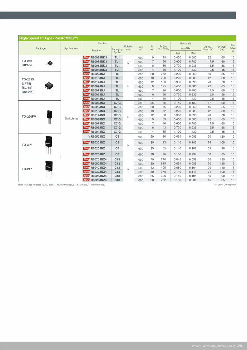
R6009JND3R6007JND3R6006JND3R6004JND3R6020JNJR6018JNJR6012JNJR6009JNJR6007JNJR6006JNJR6004JNJR6025JNXR6020JNXR6018JNXR6012JNXR6009JNXR6007JNXR6006JNXR6004JNX
R6050JNZ
R6030JNZ
R6025JNZ
R6020JNZ
R6070JNZ4R6050JNZ4R6042JNZ4R6030JNZ4R6025JNZ4R6020JNZ4
☆
0.585 0.780 0.936 1.430 0.260 0.286 0.390 0.585 0.780 0.936 1.430 0.182 0.260 0.286 0.390 0.585 0.780 0.936 1.430
0.083
0.143
0.182
0.234
0.058 0.083 0.104 0.143 0.195 0.234
0.450 0.600 0.720 1.100 0.200 0.220 0.300 0.450 0.600 0.720 1.100 0.140 0.200 0.220 0.300 0.450 0.600 0.720 1.100
0.064
0.110
0.140
0.180
0.045 0.064 0.080 0.110 0.150 0.180
125968660
2522201601259686608576726053464335
120
93
85
76
770615495370306252
ID(A)
9764
2018129764
252018129764
50
30
25
20
705042302520
VDSS
(V)
600600600600600600600600600600600600600600600600600600600
600
600
600
600
600600600600600600
Polarity(ch)
Part No.
Part No. Packaging Symbol
N
N
N
N
N
TL1TL1TL1TL1TLTLTLTLTLTLTL
C7 GC7 GC7 GC7 GC7 GC7 GC7 GC7 G
C8
C8
C8
C8
C13C13C13C13C13C13
Switching
TO-252⟨DPAK⟩
TO-263S(LPTS)[SC-83]⟨D2PAK⟩
TO-220FM
TO-3PF
TO-247
2217.515.510.55042282217.515.510.5574542282217.515.510.5
120
75
65
50
160120100746545
trr (Typ)(ns)
65605845858070656058459085807065605845
120
100
90
85
135120110100
9085
15151515151515151515151515151515151515
15
15
15
15
151515151515
☆: Under DevelopmentNote: Package indicates JEDEC code. ( )ROHM Package, [ ]JEITA Code, ⟨ ⟩General Code.
High-Speed trr type ⟨PrestoMOSTM⟩
29 Primary Power Supply Device Catalog
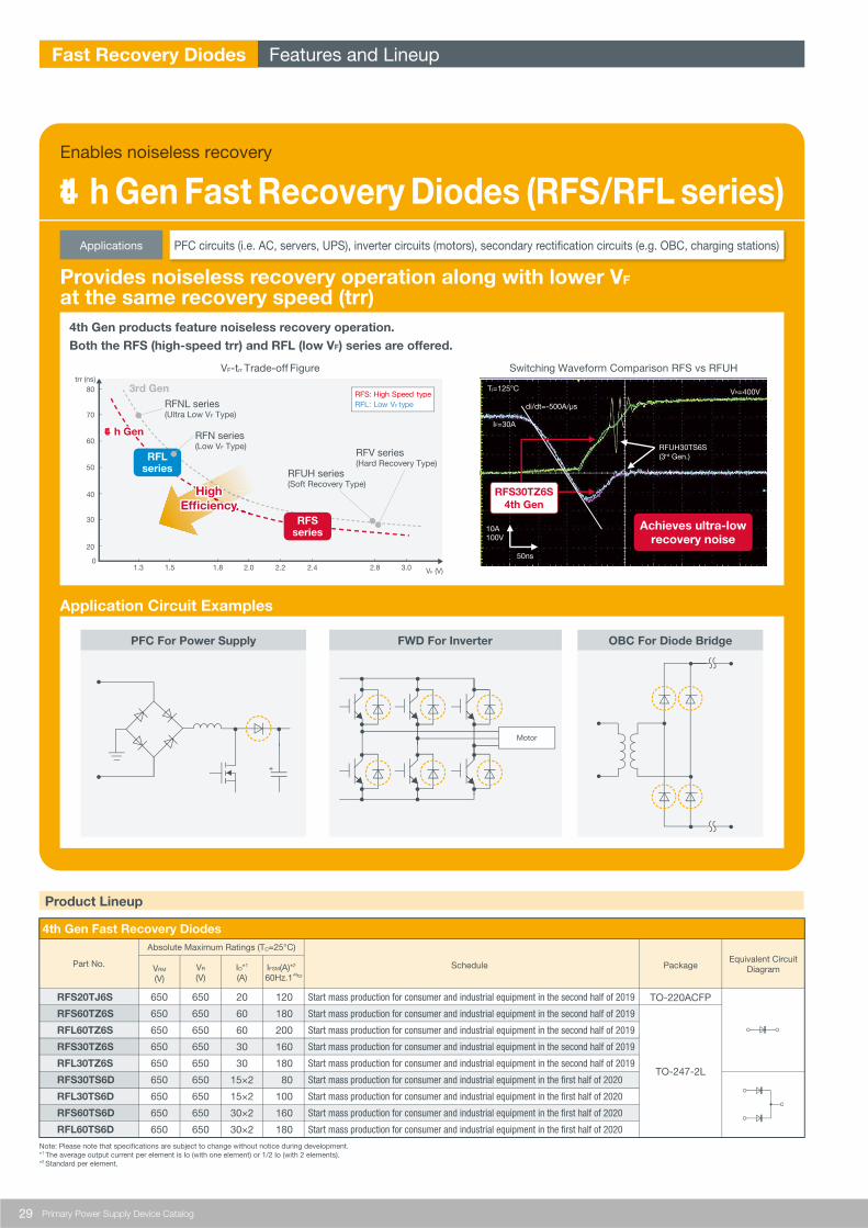
4 th Gen products feature noiseless recovery operation. Both the RFS (high-speed trr) and RFL (low VF) series are offered.
Application Circuit Examples
Switching Waveform Comparison RFS vs RFUH
Tj=125°C VR=400V
IF=30A
di/dt=-500A/μs
50ns
10A100V
Achieves ultra-lowrecovery noise
RFS30TZ 6 S4 th Gen
RFUH30TS6S(3rd Gen.)
PFC For Power Supply FWD For Inverter OBC For Diode Bridge
Motor
VF-trr Trade-off Figure
1.3 1.5 1.8 2.0 2.2 2.4 2.8 3.0
20
30
40
50
60
70
80trr (ns)
HighEfficiency
RFLseries
RFSseries
4t h Gen
3rd GenRFNL series(Ultra Low VF Type)
RFN series(Low VF Type)
RFUH series(Soft Recovery Type)
RFV series(Hard Recovery Type)
0
RFS: High Speed typeRFL: Low VF type
VF (V)
Fast Recovery Diodes
4t h Gen Fast Recovery Diodes (RFS/ RFL series)Enables noiseless recovery
PFC circuits (i.e. AC, servers, UPS), inverter circuits (motors), secondary rectification circuits (e.g. OBC, charging stations)
Provides noiseless recovery operation along with lower VF at the same recovery speed (trr)
IO*1
(A)PackageSchedule
Equivalent CircuitDiagram
RFS20TJ 6 S
RFS6 0TZ 6 S
RFL6 0TZ 6 S
RFS30TZ 6 S
RFL30TZ 6 S
RFS30TS6 D
RFL30TS6 D
RFS6 0TS6 D
RFL6 0TS6 D
TO-220ACFP
TO-247-2L
Start mass production for consumer and industrial equipment in the second half of 2019
Start mass production for consumer and industrial equipment in the second half of 2019
Start mass production for consumer and industrial equipment in the second half of 2019
Start mass production for consumer and industrial equipment in the second half of 2019
Start mass production for consumer and industrial equipment in the second half of 2019
Start mass production for consumer and industrial equipment in the first half of 2020
Start mass production for consumer and industrial equipment in the first half of 2020
Start mass production for consumer and industrial equipment in the first half of 2020
Start mass production for consumer and industrial equipment in the first half of 2020
650
650
650
650
650
650
650
650
650
650
650
650
650
650
650
650
650
650
20
60
60
30
30
15×2
15×2
30×2
30×2
120
180
200
160
180
80
100
160
180
VR
(V)VRM
(V)
Absolute Maximum Ratings (TC=25°C)
Part No.
Note: Please note that specifications are subject to change without notice during development.*1 The average output current per element is Io (with one element) or 1/2 Io (with 2 elements).*2 Standard per element.
IFSM(A)*2
60Hz.1
Features and Lineup
Applications
Product Lineup
4 th Gen Fast Recovery Diodes
30Primary Power Supply Device Catalog
3rd Gen Fast Recovery Diodes
Product Lineup
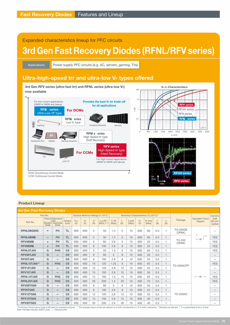
3rd Gen RFV series (ultra-fast trr) and RFN L series (ultra-low VF) now available
trr
VF
For low current applications(200W to 300W and below)
For High current applications (200W to 300W and above)
RFNL seriesUltra-Low VF type
RFN s eriesLow VF type
RFV seriesHigh-Speed trr type
(Hard Recovery)
For DCMs
For CCMs
Provides the best VF-trr trade-offfor all applications
RFUH s eriesHigh-Speed trr type
(Soft Recovery)Notebook PCs Tablets
AC
LCD-TV
Industrial Modules
Gaming Systems
VF-IF Characteristics
I F (A
)VF (mV)
0 500 1000 1500 2000 2500 3000 3500 4000 4500
0.1
1
10
100
RFNL series
RFV series
RFUH series
RFN series
Tj=25°C
50ns
5A200V
RFV series
RFU H series
IF
VR
3rd Gen Fast Recovery Diodes (RFN L/ RFV series)Expanded characteristics lineup for PFC circuits
Power supply PFC circuits (e.g. AC, servers, gaming, TVs)
U ltra-high-speed trr and ultra-low VF types offered
Part No.Packaging
Symbol
AutomotiveGrade
(AEC-Q101Qualified)
Product PerformanceCode
StandardGrade
AutomotiveGrade
Part No. Absolute Maximum Ratings (TC=25°C) Electrical Characteristics (Tj=25°C)*2
RFN L5BGE6 S
RFN L5BM6S
RFV5BM6S
RFV8BM6S
RFN L5TJ 6 S
RFVS8TJ 6 S
RFV8TJ 6 S
RFN L10TJ 6 S* 3
RFV12TJ 6 S
RFV15TJ 6 S
RFN L15TJ 6 S
RFN L20TJ 6 S
RFVS8TG6 S
RFV8TG6 S
RFV12TG6 S
RFV15TG6 S
RFV30TG6 S
*—
**G
G
G
G
G
G
G
G
G
G
G
G
G
FH
FH
FH
FH
FHG
—
—
FHG
—
—
FHG
FHG
—
—
—
—
—
TL
TL
TL
TL
C9
C9
C9
C9
C9
C9
C9
C9
C9
C9
C9
C9
C9
VRM
(V)VF (V)(Max)
IF(A)
IR (μA)(Max)
VR
(V)trr (ns)(Max)
IF(A)
IR(A)
600
600
600
600
600
600
600
600
600
600
600
600
600
600
600
600
600
VR
(V)
600
600
600
600
600
600
600
600
600
600
600
600
600
600
600
600
600
IO*1
(A)
5
5
5
8
5
8
8
10
12
15
15
20
8
8
12
15
30
50
50
60
100
50
60
100
120
120
150
160
200
60
100
120
150
200
1.3
1.3
2.8
2.8
1.3
3
2.8
1.25
2.8
2.8
1.3
1.3
3
2.8
2.8
2.8
2.8
5
5
5
8
5
8
8
8
12
15
15
20
8
8
12
15
30
10
10
10
10
10
10
10
10
10
10
10
10
10
10
10
10
10
600
600
600
600
600
600
600
600
600
600
600
600
600
600
600
600
600
60
60
20
25
60
20
25
65
25
30
65
70
20
25
25
30
40
0.5
0.5
0.5
0.5
0.5
0.5
0.5
0.5
0.5
0.5
0.5
0.5
0.5
0.5
0.5
0.5
0.5
1
1
1
1
1
1
1
1
1
1
1
1
1
1
1
1
1
TO-252GE⟨DPAK⟩
TO-252⟨DPAK⟩
TO-220ACFP
TO-220AC
—
YES
YES
YES
YES
—
—
YES
—
—
YES
YES
—
—
—
—
—
*The Product Performance Code is left blank for standard products. *1 The average output current per element is Io (with one element) or 1/2 Io (with 2 elements). *2 Standard per element. *3 VF is guaranteed at the IF 2 levelNote: Package indicates JEDEC code. ⟨ ⟩General code.
IFSM (A)*2
60Hz.1 Package
Equivalent CircuitDiagram
DCM: Dicontinuous Current ModeCCM: Continuous Current Mode
LCD TV
AC
Notebook PCs
lesLighting
Fast Recovery Diodes Features and Lineup
Applications
Servers

31 Primary Power Supply Device Catalog
Low Overshoot Noise (UDZFV/UDZGV)
Cu Gull Wing Terminals (UDZGV)
Power dissipation
Electrode Shape
DS
MP
400mW
Gull Wing
Under Development
Under Development
250mW
Flat Lead
OK
Summer 2019
UDZGV UDZFV
UDZGV series
Cu Frame
UDZFV series
Fe-Ni Frame
Zener Diodes
Series Circuit2 2.2 2.4 2.7 3 3.3 3.6 3.9 4.3 4.7 5.1 5.6 6.2 6.8 7.5 8.2 9.1 10 11 12 13 15 16 18 20 22 24 27 30 33 36 39 43 47 51 56 62 68 75 82 91 100 110 120 130 150
Vz Rank
JEDEC (ROHM)
Package PermissibleLoss(mW)
SDZ
CDZV
EDZV
UFZV
UDZV
UDZLV
UDZFV
UDZGV
TFZV
YFZV
TDZV
YDZV
BZX84B
BZX84C
KDZV
KDZLV
PDZV
PTZ
Single
Single
Single
Single
Single
Single
Single
Single
Single
Single
Single
Single
Single
Single
Single
Single
Single
Single
DSN0603-2(SMD0402)
SOD-923(VMN2M)
SOD-523(EMD2)
SOD-323FL(UMD2)
SOD-323FL(UMD2)
SOD-323FL(UMD2)
SOD-323FL(UMD2M)
SOD-323(UMD2GM)
SOD-323HE(TUMD2M)
SOD-323HE(TUMD2M)
SOD-323HE(TUMD2M)
SOD-323HE(TUMD2M)
SOT-23(SSD3)
SOT-23(SSD3)
SOD-123FL(PMDU)
SOD-123FL(PMDU)
SOD-128(PMDTM)
DO-214AC(PMDS)(SMA)
100
100
150
500
200
200
250
400
500
500
500
500
250
250
1000
1000
1000
1000
Products with improved package permissible loss will also be offered
New Series Feature ①
Zener Diodes
Cu gull wing electrodes strong against temperature cycling are used. This makes them suitable for automotive systems exposed to severe temperature environments.
Voltage fluctuations that occur during breakdown are significantly reduced compared to the existing series. This ensures safer operation in surge protection applications.
Broad Package Lineup Featuring High Reliability
Dramatically reduces voltage fluctuations that occur during breakdown over the existing UDZVxx series-ideal for surge protection applications
Comparison of Breakdown Noise7
5.3
3.5
1.8
0UDZVxx UDZFVxx UDZGVxx
60%Down60%Down
80%Down80%Down
Automotive Grade
☆
New Series Feature ②
Zener Diode Breakdown WaveformVertical100.0μA/div
Horizontal5.00V/div
Step Gen(A/V)50.0nA/Step
Step Offset0.00A
AUX SUPPLY0.00V V
cl (V
)
30
25
20
15
10
5
0
–5
time (ms)
15 20 25 30 35 40 45 50–10 –5 0 5 10
Vcl-time CHARACTERISTICS
Bre
ak d
own
nois
e (V
)
Vz
Iz
Features and Lineup
☆: Under Development

32Primary Power Supply Device Catalog
Part No.(Standard Grade)
Vz(V)
Schedule
Schedule
Min Typ Max StandardGrade
Automotive-GradeProduct
StandardGrade
Automotive-GradeProduct
DS CSMP
UDZFVTE-173.6B
UDZFVTE-173.9B
UDZFVTE-174.3B
UDZFVTE-174.7B
UDZFVTE-175.1B
UDZFVTE-175.6B
UDZFVTE-176.2B
UDZFVTE-176.8B
UDZFVTE-177.5B
UDZFVTE-178.2B
UDZFVTE-179.1B
UDZFVTE-1710B
UDZFVTE-1711B
UDZFVTE-1712B
UDZFVTE-1713B
UDZFVTE-1715B
UDZFVTE-1716B
UDZFVTE-1718B
UDZFVTE-1720B
UDZFVTE-1722B
UDZFVTE-1724B
UDZFVTE-1727B
UDZFVTE-1730B
UDZFVTE-1733B
UDZFVTE-1736B
Part No.(Automotive-Grade Product)
Pd(W)
Iz(mA)
UDZFVFHTE-173.6B
UDZFVFHTE-173.9B
UDZFVFHTE-174.3B
UDZFVFHTE-174.7B
UDZFVFHTE-175.1B
UDZFVFHTE-175.6B
UDZFVFHTE-176.2B
UDZFVFHTE-176.8B
UDZFVFHTE-177.5B
UDZFVFHTE-178.2B
UDZFVFHTE-179.1B
UDZFVFHTE-1710B
UDZFVFHTE-1711B
UDZFVFHTE-1712B
UDZFVFHTE-1713B
UDZFVFHTE-1715B
UDZFVFHTE-1716B
UDZFVFHTE-1718B
UDZFVFHTE-1720B
UDZFVFHTE-1722B
UDZFVFHTE-1724B
UDZFVFHTE-1727B
UDZFVFHTE-1730B
UDZFVFHTE-1733B
UDZFVFHTE-1736B
0.25Summer
2019
Under Development
3.6
3.89
4.17
4.55
4.98
5.49
6.06
6.65
7.28
8.02
8.85
9.77
10.76
11.74
12.91
14.34
15.85
17.56
19.52
21.54
23.72
26.19
29.19
32.15
35.07
3.6
3.9
4.3
4.7
5.1
5.6
6.2
6.8
7.5
8.2
9.1
10
11
12
13
15
16
18
20
22
24
27
30
33
36
3.845
4.16
4.43
4.75
5.2
5.73
6.33
6.93
7.6
8.36
9.23
10.21
11.22
12.24
13.49
14.98
16.51
18.35
20.39
22.47
24.78
27.53
30.69
33.79
36.87
5
5
5
5
5
5
5
5
5
5
5
5
5
5
5
5
5
5
5
5
5
5
5
5
5
OK
OK
OK
OK
OK
OK
OK
OK
OK
OK
OK
OK
OK
OK
OK
—
OK
OK
OK
OK
OK
—
OK
OK
OK
—
—
—
OK
—
OK
OK
—
—
—
—
—
—
—
—
OK
OK
OK
—
—
—
OK
OK
—
—
OK
OK
OK
OK
OK
OK
OK
OK
OK
OK
OK
OK
OK
OK
OK
OK
OK
OK
OK
OK
OK
OK
OK
OK
OK
OK
OK
OK
OK
OK
OK
OK
OK
OK
OK
OK
OK
OK
OK
OK
OK
OK
OK
OK
OK
OK
OK
OK
OK
OK
Part No.(Standard Grade)
Vz(V)
Min Typ Max
UDZGVTE-173.6B
UDZGVTE-173.9B
UDZGVTE-174.3B
UDZGVTE-174.7B
UDZGVTE-175.1B
UDZGVTE-175.6B
UDZGVTE-176.2B
UDZGVTE-176.8B
UDZGVTE-177.5B
UDZGVTE-178.2B
UDZGVTE-179.1B
UDZGVTE-1710B
UDZGVTE-1711B
UDZGVTE-1712B
UDZGVTE-1713B
UDZGVTE-1715B
UDZGVTE-1716B
UDZGVTE-1718B
UDZGVTE-1720B
UDZGVTE-1722B
UDZGVTE-1724B
UDZGVTE-1727B
UDZGVTE-1730B
UDZGVTE-1733B
UDZGVTE-1736B
☆☆☆☆☆☆☆☆☆☆☆☆☆☆☆☆☆☆☆☆☆☆☆☆☆
☆☆☆☆☆☆☆☆☆☆☆☆☆☆☆☆☆☆☆☆☆☆☆☆☆
Part No.(Automotive-Grade Product)
Pd(W)
Iz(mA)
UDZGVFHTE-173.6B
UDZGVFHTE-173.9B
UDZGVFHTE-174.3B
UDZGVFHTE-174.7B
UDZGVFHTE-175.1B
UDZGVFHTE-175.6B
UDZGVFHTE-176.2B
UDZGVFHTE-176.8B
UDZGVFHTE-177.5B
UDZGVFHTE-178.2B
UDZGVFHTE-179.1B
UDZGVFHTE-1710B
UDZGVFHTE-1711B
UDZGVFHTE-1712B
UDZGVFHTE-1713B
UDZGVFHTE-1715B
UDZGVFHTE-1716B
UDZGVFHTE-1718B
UDZGVFHTE-1720B
UDZGVFHTE-1722B
UDZGVFHTE-1724B
UDZGVFHTE-1727B
UDZGVFHTE-1730B
UDZGVFHTE-1733B
UDZGVFHTE-1736B
0.4
3.47
3.76
4.17
4.61
5
5.49
6.08
6.66
7.35
8.04
8.92
9.8
10.78
11.76
12.74
14.7
15.68
17.64
19.6
21.56
23.52
26.33
29.25
32.18
35.1
3.6
3.9
4.3
4.7
5.1
5.6
6.2
6.8
7.5
8.2
9.1
10
11
12
13
15
16
18
20
22
24
27
30
33
36
3.73
4.04
4.43
4.79
5.2
5.71
6.32
6.94
7.65
8.36
9.28
10.2
11.22
12.24
13.26
15.3
16.32
18.36
20.4
22.44
24.48
27.68
30.75
33.83
36.9
5
5
5
5
5
5
5
5
5
5
5
5
5
5
5
5
5
5
5
5
5
2
2
2
2☆: Under Development
UDZFV series
UDZGV series
New series Product Lineup
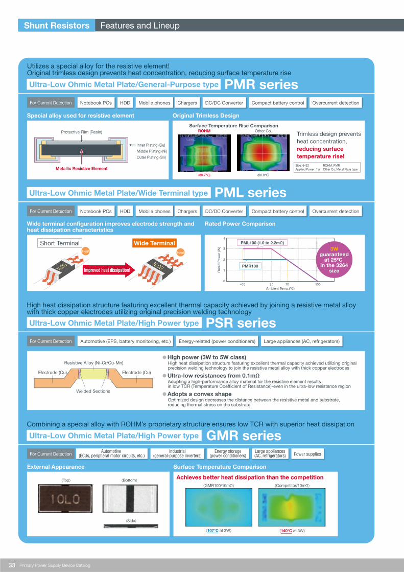
33 Primary Power Supply Device Catalog
Utilizes a special alloy for the resistive element! Original trimless design prevents heat concentration, reducing surface temperature rise
High heat dissipation structure featuring excellent thermal capacity achieved by joining a resistive metal alloy with thick copper electrodes utilizing original precision welding technology
Original Trimless DesignSpecial alloy used for resistive element
Short TerminalHeat
Wide Terminal
Improved heat dissipation!
Heat
Imp n!
Heat
●High power (3W to 5W class)High heat dissipation structure featuring excellent thermal capacity achieved utilizing originalprecision welding technology to join the resistive metal alloy with thick copper electrodes
●Ultra-low resistances from 0.1mΩAdopting a high-performance alloy material for the resistive element results in low TCR (Temperature Coefficient of Resistance)-even in the ultra-low resistance region
●Adopts a convex shapeOptimized design decreases the distance between the resistive metal and substrate, reducing thermal stress on the substrate
Resistive Alloy (Ni-Cr/Cu-Mn)
Welded Sections
Electrode (Cu) Electrode (Cu)
Combining a special alloy with ROHM’s proprietary structure ensures low TCR with superior heat dissipation
Achieves better heat dissipation than the competition⟨Top⟩ ⟨Bottom⟩
⟨Side⟩
Automotive (EPS, battery monitoring, etc.) Energy-related (power conditioners) Large appliances (AC, refrigerators)
Automotive (ECUs, peripheral motor circuits, etc.)
Industrial(general-purpose inverters)
Energy storage(power conditioners)
Large appliances(AC, refrigerators) Power supplies
Shunt Resistors
Trimless design prevents heat concentration,reducing surface temperature rise!
ROHM
(88.7ºC) (98.8ºC)
Other Co.
Size: 6432Applied Power: 1W
ROHM: PMROther Co: Metal Plate type
Surface Temperature Rise Comparison
For Current Detection Notebook PCs Mobile phones Chargers DC/DC Converter Compact battery control Overcurrent detectionHDD
For Current Detection
For Current Detection
For Current Detection
Notebook PCs Mobile phones Chargers DC/DC Converter Compact battery control Overcurrent detectionHDD
Wide terminal configuration improves electrode strength andheat dissipation characteristics
Rated Power Comparison
PML100 (1.0 to 2.2mΩ)
PMR100
Ambient Temp.(ºC)–55 25 70 155
0
1
2
3
4
Rat
ed P
ower
(W) 3W
guaranteedat 25ºC
in the 3264size
Surface Temperature ComparisonExternal Appearance
⟨107°C at 3W⟩
⟨GMR100/10mΩ⟩
⟨140°C at 3W⟩
⟨Competitor/10mΩ⟩
Ultra-Low Ohmic Metal Plate/General-Purpose type PMR series
Ultra-Low Ohmic Metal Plate/High Power type GMR series
Ultra-Low Ohmic Metal Plate/High Power type
Ultra-Low Ohmic Metal Plate/Wide Terminal type PML series
PSR series
Inner Plating (Cu)
Middle Plating (Ni)
Outer Plating (Sn)
Protective Film (Resin)
Metallic Resistive Element
Features and Lineup
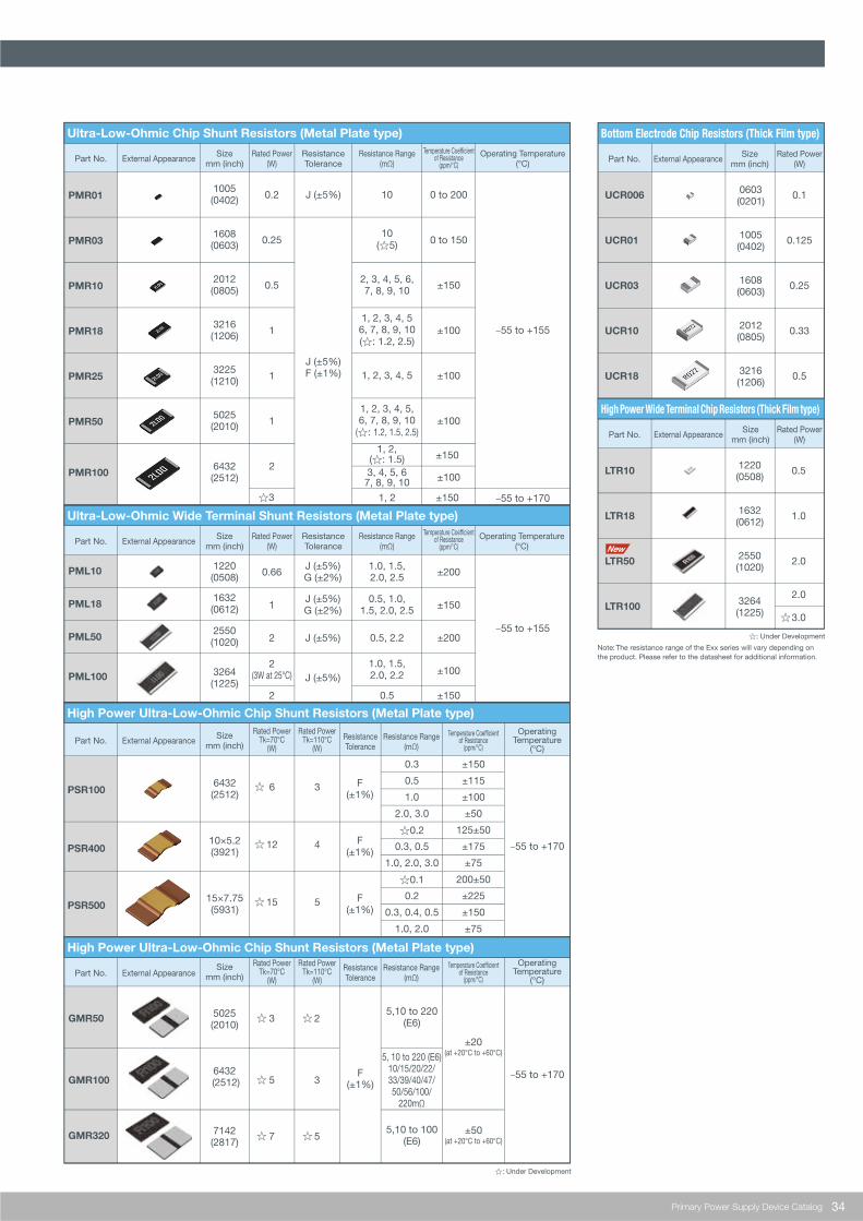
34Primary Power Supply Device Catalog
Ultra-Low-Ohmic Chip Shunt Resistors (Metal Plate type) Bottom Electrode Chip Resistors (Thick Film type)
Ultra-Low-Ohmic Wide Terminal Shunt Resistors (Metal Plate type)
High Power Ultra-Low-Ohmic Chip Shunt Resistors (Metal Plate type)
High Power Ultra-Low-Ohmic Chip Shunt Resistors (Metal Plate type)
High Power Wide Terminal Chip Resistors (Thick Film type)
Part No. External AppearanceSize
mm (inch)Rated Power
(W)ResistanceTolerance
Resistance Range(mΩ)
Temperature Coefficientof Resistance
(ppm/°C)Operating Temperature
(°C)
PMR01
PMR03
PMR10
PMR18
PMR25
PMR50
1005(0402) 0.2
0.25
0.5
1
1
1
2
J (±5%)
J (±5%)F (±1%)
1608(0603)
2012(0805)
3216(1206)
3225(1210)
5025(2010)
10
10(☆5)
2, 3, 4, 5, 6,7, 8, 9, 10
1, 2, 3, 4, 56, 7, 8, 9, 10(☆: 1.2, 2.5)
1, 2, 3, 4, 5
1, 2, 3, 4, 5,6, 7, 8, 9, 10
(☆: 1.2, 1.5, 2.5)
1, 2,(☆: 1.5)3, 4, 5, 67, 8, 9, 10
1, 2
±150
±100
±150
6432(2512)
☆3
0 to 200
0 to 150
±150
±100
±100
±100
−55 to +155
−55 to +170
Sizemm (inch)
Rated Power(W)Part No. External Appearance
0603(0201)
1005(0402)
1608(0603)
2012(0805)
1220(0508)
1632(0612)
2550(1020)
3264(1225)
3216(1206)
UCR006
UCR01
UCR03
UCR10
UCR18
0.1
0.125
0.25
0.33
0.5
Part No. External AppearanceSize
mm (inch)Rated Power
(W)ResistanceTolerance
Resistance Range(mΩ)
Temperature Coefficientof Resistance
(ppm/°C)Operating Temperature
(°C)
1220(0508)
1632(0612)
2550(1020)
3264(1225)
PML10
PML18
PML50
PML100
1.0, 1.5,2.0, 2.5
J (±5%)G (±2%)
J (±5%)G (±2%)
J (±5%)
J (±5%)
0.5, 1.0,1.5, 2.0, 2.5
0.5, 2.2
1.0, 1.5,2.0, 2.2
0.5
±200
±150
±200
±100
±150
0.66
1
2
2
2(3W at 25°C)
−55 to +155
Part No. External AppearanceSize
mm (inch)
Rated PowerTk=110°C
(W)ResistanceTolerance
Resistance Range(mΩ)
Temperature Coefficientof Resistance
(ppm/°C)
OperatingTemperature
(°C)
0.3
0.5
1.0
2.0, 3.0
☆0.2
0.3, 0.5
1.0, 2.0, 3.0
☆0.1
0.2
0.3, 0.4, 0.5
1.0, 2.0
±150
±115
±100
±50
125±50
±175
±75
200±50
±225
±150
±75
F(±1%)
F(±1%)
F(±1%)
6432(2512)
10×5.2(3921)
15×7.75(5931)
PSR100
PSR400
PSR500
3
4
5
−55 to +170
Part No. External AppearanceSize
mm (inch)
Rated PowerTk=110°C
(W)
ResistanceTolerance
Resistance Range(mΩ)
Temperature Coefficientof Resistance
(ppm/°C)
OperatingTemperature
(°C)
5025(2010)
F(±1%)
2
3
GMR50
GMR100
GMR320
6432 (2512)
7142(2817)
5,10 to 220(E6)
5, 10 to 220 (E6)10/15/20/22/33/39/40/47/50/56/100/
220mΩ
5,10 to 100(E6)
±20(at +20°C to +60°C)
±50(at +20°C to +60°C)
−55 to +170
Sizemm (inch)
Rated Power(W)Part No. External Appearance
☆
LTR10
LTR18
LTR50
LTR100
0.5
1.0
2.0
PMR100
5
Rated PowerTk=70°C
(W)
6
12
15
☆
☆
☆
Rated PowerTk=70°C
(W)
3
5
7
☆
☆
☆
☆
☆
☆: Under Development
2.0
3.0
☆: Under Development
Note: The resistance range of the Exx series will vary depending on the product. Please refer to the datasheet for additional information.
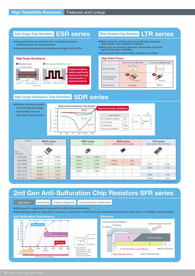
35 Primary Power Supply Device Catalog
2nd Gen Anti-Sulfuration Chip Resistors SFR series
High Surge Resistance
■Standard typeInternal Electrode
Current flow
Resistive ElementLaser Trim Current flow Resistive Element
■Anti-Surge Resistance type
Original resistance pattern significantly improves anti-surge characteristics vs standard products
●Supports higher power than the conventional series, contributing to set miniaturization
●Guaranteed electrostatic breakdown voltage: 2kV to 5kV
Cross Sectional Diagram
Test Conditions・Temperature: 110°C・Sulfur powder: 10g・Desiccator used・Criteria: ΔR≧100%
Sulfur(10g) Specimen
Desiccator
Oven 110°C
100
90
80
70
60
50
40
30
20
1
00 500 1000 1500 2000 2500 3000
Time (h)
Standard Type
1st GenAnti-Sulfuration Products
SFR series
1st GenAnti-SulfurationProduct Lifetime: 750hrs
SFR series: Over 3000hrs
Bur
nout
Rat
io (%
) Sn Plating Ni Plating
Sulfurizing gas entry point
Resistive Element
Upper Electrode (Ag)
② Anti-Sulfuration Layer (Resin)
① Side Electrode (Ni-Cr)
Overcoat (Resin)
Applications Automotive Industrial equipment Communications infrastructure
High Reliability Resistors
Sizemm (inch)
1005 (0402)
1608 (0603)
2012 (0805)
3216 (1206)
3225 (1210)
5025 (2010)
6432 (2512)
MCR01
MCR03
MCR10
MCR18
MCR25
MCR50
MCR100
0.063W
0.10W
0.125W
0.25W
0.25W
0.50W
1.0W
ESR01
ESR03
ESR10
ESR18
ESR25
—
—
0.20W
0.25W
0.40W
0.5W
0.66W
—
—
—
SDR03
SDR10
—
—
—
—
—
0.3W
0.5W
—
—
—
—
—
—
LTR10
LTR18
—
LTR50
LTR100
—
—
0.25W
0.75W
—
1.0W
2.0W
Series MCR series(Standard)
ESR series(High power)
SDR series(High power) (Anti-surge)
LTR series(High power) (Wide terminal)
●Optimized for applications exposed to sulfur-rich environments●Dramatically improves sulfuration resistance compared to conventional anti-sulfuration products (by more than 3x in ROHM’s standard tests)
Anti-Sulfuration Performance Structure
Electrostatic Breakdown Test Results
1MΩ100KΩ10KΩ1KΩ100Ω10Ω
5%
0%
–5%
–10%
–15%
–20%
–25%Res
ista
nce
Cha
nge
Rat
e (⊿
R /
R )
MMCRCR03MCR03
ESESR03ESR03
SDR03SDR03Improved surge resistance
Test Condition
DC V (Applied Voltage) 3kV
No. of Cycles ±10
C (Capacitor) 100pF
R (Discharge Resistor) 1.5kΩ
R1
DCV SampleC
●Original resistance pattern and trimming technology significantly improves anti-surge characteristics
High Rated Power
WideTerminal LTR series Conventional MCR series
Electrode Size
Heat Dissipation to Substrate
Rated Power Excellent Better
Large Small
heatheat
Superior Standard
Anti-Surge Chip Resistors
High Surge Resistance Chip Resistors
☆
☆: Under Development
Features and Lineup
ESR series Wide Terminal Chip Resistors LTR series
SDR series
●Wide terminal configuration dramatically increases rated power over standard products
●Reducing the distance between electrodes results in superior junction reliability
●Guaranteed 3kV electrostatic breakdown voltage
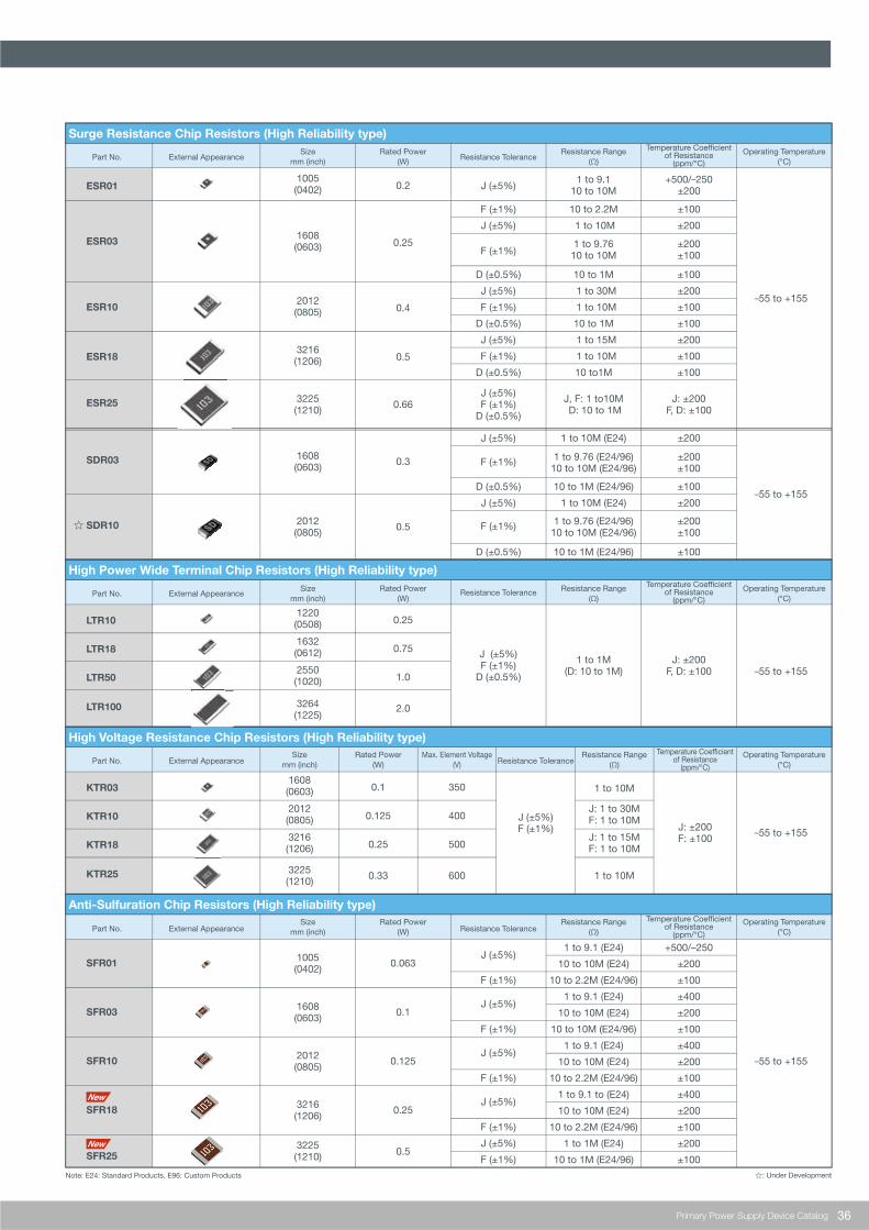
36Primary Power Supply Device Catalog
Part No. External AppearanceSize
mm (inch)Rated Power
(W) Resistance ToleranceResistance Range
(Ω)
Temperature Coefficientof Resistance
(ppm/°C)
Operating Temperature(°C)
ESR01
ESR03
ESR10
ESR18
ESR25
1005(0402)
1608(0603)
2012(0805)
3216(1206)
3225(1210)
0.2
0.25
0.4
0.5
0.66
J (±5%)
F (±1%)
J (±5%)
F (±1%)
D (±0.5%)
J (±5%)
F (±1%)
D (±0.5%)
J (±5%)
F (±1%)
D (±0.5%)
10 to 1M
1 to 30M
1 to 10M
10 to 1M
1 to 15M
1 to 10M
10 to1M
±100
±200
±100
±100
±200
±100
±100
J (±5%)F (±1%)
D (±0.5%)
J, F: 1 to10M D: 10 to 1M
J: ±200F, D: ±100
1 to 9.110 to 10M
1 to 9.7610 to 10M
±200±100
+500/–250±200
Part No. External AppearanceSize
mm (inch)Rated Power
(W)Resistance Tolerance Resistance Range
(Ω)
Temperature Coefficientof Resistance
(ppm/°C)Operating Temperature
(°C)
LTR10
LTR18
LTR50
1220(0508)
1632(0612)
2550(1020)
3264(1225)
0.25
0.75
1.0
2.0
J (±5%)F (±1%)
D (±0.5%)
1 to 1M(D: 10 to 1M)
J: ±200F, D: ±100
10 to 2.2M
1 to 10M
±100
±200
☆: Under DevelopmentNote: E24: Standard Products, E96: Custom Products
–55 to +155
SDR03
SDR10☆
1608(0603)
2012(0805)
0.3
0.5
±100
±100
±200
±200±100
±200±100
±200
10 to 1M (E24/96)
10 to 1M (E24/96)
1 to 10M (E24)
1 to 9.76 (E24/96)10 to 10M (E24/96)
1 to 9.76 (E24/96)10 to 10M (E24/96)
1 to 10M (E24)
D (±0.5%)
D (±0.5%)
J (±5%)
F (±1%)
F (±1%)
J (±5%)
–55 to +155
Part No. External AppearanceSize
mm (inch)Rated Power
(W) Resistance ToleranceResistance Range
(Ω)
Temperature Coefficientof Resistance
(ppm/°C)
Operating Temperature(°C)
SFR01
SFR03
SFR10
SFR18
SFR25
1005(0402)
1608(0603)
2012(0805)
3216(1206)
3225(1210)
0.063
0.1
0.125
0.25
0.5
F (±1%)
J (±5%)
F (±1%)
J (±5%)
F (±1%)
J (±5%)
F (±1%)
J (±5%)
F (±1%)
J (±5%)
1 to 9.1 (E24)
10 to 10M (E24)
10 to 2.2M (E24/96)
1 to 9.1 (E24)
10 to 10M (E24)
10 to 10M (E24/96)
1 to 9.1 (E24)
10 to 10M (E24)
10 to 2.2M (E24/96)
1 to 9.1 to (E24)
10 to 10M (E24)
10 to 2.2M (E24/96)
1 to 1M (E24)
10 to 1M (E24/96)
+500/–250
±200
±100
±400
±200
±100
±400
±200
±100
±400
±200
±100
±200
±100
–55 to +155
–55 to +155
Part No. External AppearanceSize
mm (inch)Rated Power
(W) Resistance ToleranceResistance Range
(Ω)
Temperature Coefficientof Resistance
(ppm/°C)
Operating Temperature(°C)
KTR03
KTR10
KTR18
1608(0603)
2012(0805)
3216(1206)
3225(1210)
0.1
0.125
0.25
0.33
Max. Element Voltage(V)
350
400
500
J (±5%)F (±1%)
1 to 10M
J: 1 to 30MF: 1 to 10M
J: 1 to 15MF: 1 to 10M
1 to 10M
J: ±200F: ±100
–55 to +155
LTR100
KTR25 600
Surge Resistance Chip Resistors (High Reliability type)
High Power Wide Terminal Chip Resistors (High Reliability type)
High Voltage Resistance Chip Resistors (High Reliability type)
Anti-Sulfuration Chip Resistors (High Reliability type)

37 Primary Power Supply Device Catalog
Sales OfficesManufacturing FacilitiesR&D CentersDistribution Centers
KyotoTokyoYokohama
NagoyaMatsumotoMito
Nishi-TokyoSendaiTakasaki
Utsunomiya
● Sales Offices
ROHM Co., Ltd.ROHM Shiga Co., Ltd.ROHM Hamamatsu Co., Ltd.ROHM Wako Co., Ltd.ROHM Apollo Co., Ltd.ROHM Mechatech Co., Ltd.LAPIS Semiconductor Co., Ltd.LAPIS Semiconductor Miyagi Co., Ltd.LAPIS Semiconductor Miyazaki Co., Ltd.
● Manufacturing Facilities
Kyoto Technology Center (Head Office)Kyoto Technology Center (Kyoto Ekimae)Yokohama Technology CenterLAPIS Semiconductor Co., Ltd.(Shin-Yokohama)LAPIS Semiconductor Miyazaki Design Center
ROHM Logistec Co., Ltd.
● Distribution Centers
● R&D Centers
Kyoto (Headquarters)Kyoto (Headquarters) Kyoto Technology CenterKyoto Technology Center Yokohama Technology CenterYokohama Technology CenterLAPIS Semiconductor
Miyazaki Co., Ltd.LAPIS Semiconductor
Miyazaki Co., Ltd.
LAPIS Semiconductor Miyagi Co., Ltd.
LAPIS Semiconductor Miyagi Co., Ltd.
ROHM Group Locations (Japan)
Sendai
Nishi-Tokyo
TakasakiMatsumoto
ROHM Hamamatsu Co., Ltd.(Shizuoka)
NagoyaROHM Shiga Co., Ltd.(Shiga)
ROHM (Headquarters)Kyoto
ROHM Mechatech Co., Ltd.(Kyoto)
ROHM Apollo Co., Ltd.(Fukuoka)
LAPIS Semiconductor Miyagi Co., Ltd. (Miyagi)
Mito
TokyoLAPIS Semiconductor (Headquarters)Yokohama
LAPIS Semiconductor Miyazaki Co., Ltd.(Miyazaki)
LAPIS Semiconductor Miyazaki Design Center(Miyazaki)
Utsunomiya
ROHM Logistec Co., Ltd.(Okayama)
ROHM Wako Co., Ltd.(Okayama)

38Primary Power Supply Device Catalog
●● Sales Offices
ROHM Semiconductor Korea CorporationROHM Semiconductor Trading (Dalian) Co., Ltd.ROHM Semiconductor Trading (Beijing) Co., Ltd.ROHM Semiconductor (Shanghai) Co., Ltd.ROHM Semiconductor (Shenzhen) Co., Ltd.ROHM Semiconductor Hong Kong Co., Ltd.ROHM Semiconductor Taiwan Co., Ltd.ROHM Semiconductor Singapore Pte. Ltd.ROHM Semiconductor Philippines CorporationROHM Semiconductor (Thailand) Co., Ltd.ROHM Semiconductor Malaysia Sdn. Bhd.ROHM Semiconductor India Pvt. Ltd.ROHM Semiconductor U.S.A., LLCROHM Semiconductor GmbH
AMERICAEUROPE
ASIA
● R&D Centers
Korea Design CenterBeijing Design CenterShanghai Design Center Shenzhen Design Center Taiwan Design CenterIndia Design Center America Design Center (Santa Clara) Europe Design CenterFinland Software Development CenterROHM POWERVATION Ltd.
AMERICAEUROPE
ASIA
● Manufacturing Facilities
ROHM Korea CorporationROHM Electronics Philippines, Inc.ROHM Integrated Systems (Thailand) Co., Ltd.ROHM Semiconductor (China) Co., Ltd.ROHM Electronics Dalian Co., Ltd.ROHM-Wako Electronics (Malaysia) Sdn. Bhd.ROHM Mechatech Philippines, Inc.ROHM Mechatech (Thailand) Co., Ltd.Kionix, Inc.SiCrystal GmbH
AMERICAEUROPE
ASIA
● QA Centers
Korea QA Center Shanghai QA Center Shenzhen QA Center Taiwan QA CenterThailand QA Center Americas QA CenterEurope QA Center
AMERICAEUROPE
ASIA
Sales OfficesManufacturing FacilitiesR&D CentersQA Centers
ROHM Group Locations (Global)
GermanySiCrystal
India
ROHM Integrated Systems (Thailand)ROHM Mechatech (Thailand)
Thailand
ROHM-Wako Electronics (Malaysia)PhilippinesTaiwanShanghai
Korea
ROHM Electronics DalianROHM Semiconductor (China)
Finland
ROHM Mechatech PhilippinesMalaysiaSingapore
ShenzhenHong Kong
KionixDetroit
ROHM Electronics Philippines
U.S.A.Santa Clara
Beijing

August 1st, 2019.
Catalog No.62P7223E-B 12.2019 PDF © 2019 ROHM Co., Ltd.