principles of semiconductor devices i
TRANSCRIPT

Semiconductor Devises Physics & Fabrications
PhotolithographyLecture 16
Khosrow GhadiriElectrical Engineering Department
San Jose State University

© Khosrow Ghadiri Solid State Devices-EE Dept. SJSU 2
PhotolithographyLithographic overviewResolutionDepth of FocusOverlay ErrorsPhotoresist ResponseE-beam and X-ray lithography

© Khosrow Ghadiri Solid State Devices-EE Dept. SJSU 3
PhotolithographyPhotolithography can be divided into three steps:
1. Design using CAD systemLayoutSimulationDesign Rule Verification
2. Mask making
3. Wafer exposureThe patterns transfer form mask to photo resistChemical or plasma etching to transfer thepattern from the photo resist to burrier materialon the surface of wafer.
Light Source
CondenserLens
Mask
ReductionLens
Wafer
Wafer Exposure
© Khosrow Ghadiri Solid State Devices-EE Dept. SJSU 4
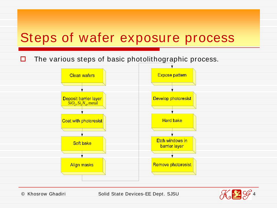
Steps of wafer exposure processThe various steps of basic photolithographic process.
2 3 4, ,metalSiO Si N

© Khosrow Ghadiri Solid State Devices-EE Dept. SJSU 5
Silicon wafern or p-type silicon wafer are available with a specified resistivelyTypically the growing crystal is doped with boron, phosphorous or arsenic. Arsenic and antimony is used for low resistively (high concentration) n-type crystal.The thickness The diameter (wafers with diameter of 1,1.5,2,3,4,5 and 6 inches have been used at various stages in history of solid state devices).The diameter of wafer is chosen in order to withstand the mechanical and thermal strain during the process steps. (for example a 6 to 8 inch diameter semiconductor wafer needs to be about thick.
250 500m t mμ μ≤ ≤( ) ( )200 8 inch 300 12 inchmm d mm≤ ≤
500 mμ
© Khosrow Ghadiri Solid State Devices-EE Dept. SJSU 6
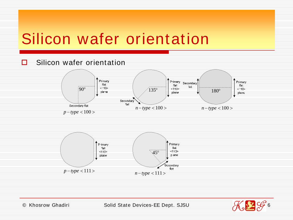
Silicon wafer orientationSilicon wafer orientation
90°
100p type− < >
111p type− < >
135°
100n type− < >
111n type− < >
45°
100n type− < >
180°

© Khosrow Ghadiri Solid State Devices-EE Dept. SJSU 7
A wafer through the various steps of the photolithography process
Various steps of the photolithography process

© Khosrow Ghadiri Solid State Devices-EE Dept. SJSU 8
Lithographic exposure systemSchematic of a simple lithographic exposure system
OpticalSource
Aperture
Shutter
Mask
Resistwafer

© Khosrow Ghadiri Solid State Devices-EE Dept. SJSU 9
Lithographic exposure system(a) Contact printing, in which wafer is in intimate contact with mask, (b) proximity printing, in which wafer and mask are in close proximity (c) projection printing, in which light source is scanned across the mask and focused on the wafer.
WaferSiO2
Mask
Lens
Ultravioletlight
source
WaferPhotoresist
Space
WaferSiO2
Photoresist
Lens 2
Mask
Lens 1
(C)
(b)(a)

© Khosrow Ghadiri Solid State Devices-EE Dept. SJSU 10
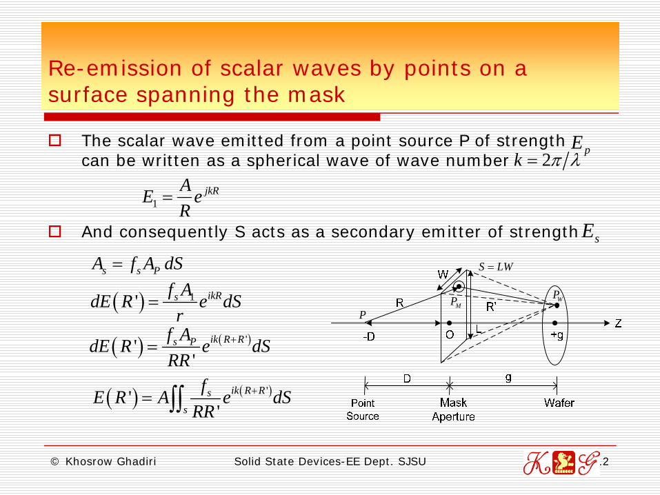
Re-emission of scalar waves by points on a surface spanning the mask
The light propagates as an electromagnetic wave, where it can be represented by its electric field
Where is the electric field amplitude, is the position, is the phase and is the frequency of the wave
WPMP
S LW=
P
( ) ( ) ( ),0, j r fE r f E r e φ=
( )( )jk R R
S
A eE R j d SR Rλ
′− +
′ =′∫∫
* 20 0 0
j jI EE E e E e Eφ φ−= = =
0E r φf

© Khosrow Ghadiri Solid State Devices-EE Dept. SJSU 11
Re-emission of scalar waves by points on a surface spanning the mask
Consider the amplitude E observed at a point arising from light emitted from a point source and scattered by a plane mask S.If an element of area at on plane mask is distributed by a wave amplitude this same point acts as a coherent secondary emitter of strength Where is called the transmission function of S at pointIn the simplest examples is zero where the mask isopaque and unity where it istransparent.
WPMP
S LW=
P
MP
sf
sf
dS
WPMP
MP
1EdsEfS 1
© Khosrow Ghadiri Solid State Devices-EE Dept. SJSU 12
Re-emission of scalar waves by points on a surface spanning the mask
The scalar wave emitted from a point source P of strength can be written as a spherical wave of wave number
And consequently S acts as a secondary emitter of strength
WPMP
S LW=
P( ) 1' ikRsf AdE R e dS
r=
1jkRAE e
R=
s s PA f A dS=
2k π λ=
( ) ( )'''
ik R Rs Pf AdE R e dSRR
+=
( ) ( )'''
ik R Rss
fE R A e dSRR
+= ∫∫
sE
pE

© Khosrow Ghadiri Solid State Devices-EE Dept. SJSU 13
Nearfield or Fresnel diffractionThe solution of equation
is photolithography is only considered in two limiting cases.1- Nearfield or Fresnel diffraction, if the above equation is solved subject to the simplifying assumption that
where W is the width of aperture, is wavelength of incoming light, is the distance form mask aperture to surface of wafer and finally r is the radial distance between the center of the diffraction pattern and the observation point.
( )( )jk R R
S
A eE R j dSRRλ
′− +
′ =′∫∫
2 2 2W g rλ +
λg
© Khosrow Ghadiri Solid State Devices-EE Dept. SJSU 14
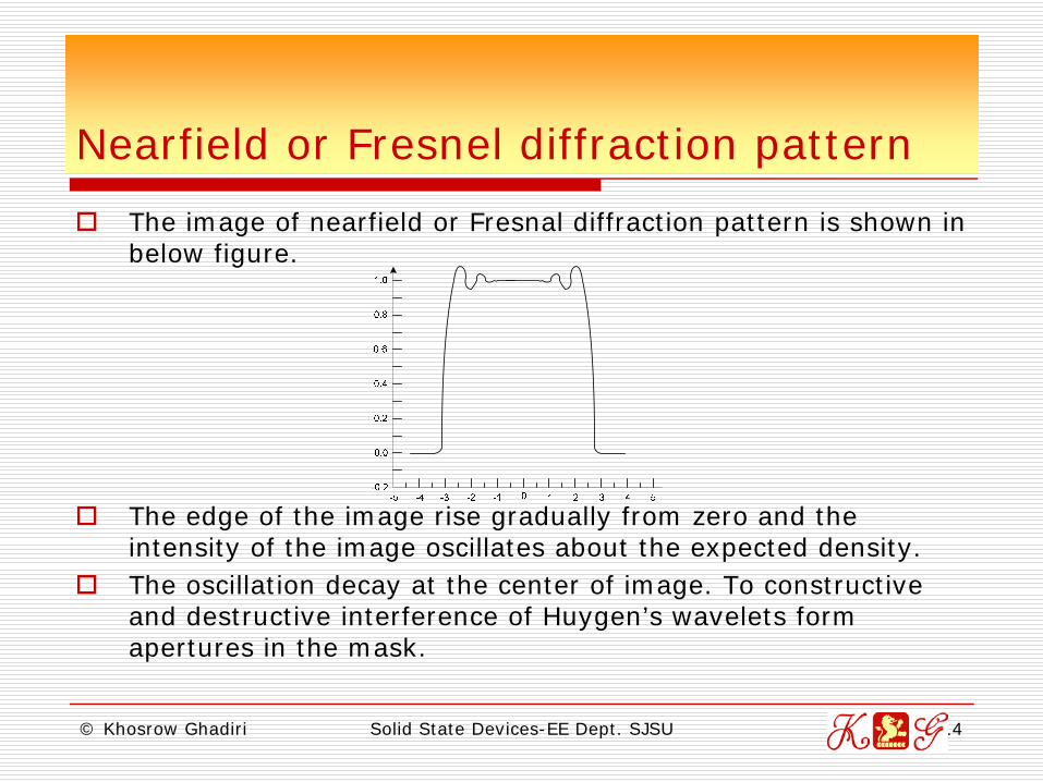
Nearfield or Fresnel diffraction pattern
The image of nearfield or Fresnal diffraction pattern is shown in below figure.
The edge of the image rise gradually from zero and the intensity of the image oscillates about the expected density.The oscillation decay at the center of image. To constructive and destructive interference of Huygen’s wavelets form apertures in the mask.
© Khosrow Ghadiri Solid State Devices-EE Dept. SJSU 15
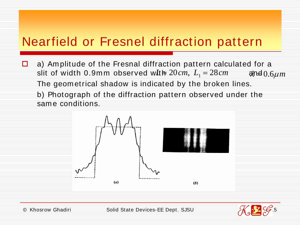
Nearfield or Fresnel diffraction pattern
a) Amplitude of the Fresnal diffraction pattern calculated for a slit of width 0.9mm observed with and The geometrical shadow is indicated by the broken lines. b) Photograph of the diffraction pattern observed under the same conditions.
120 , 28L cm L cm= = 0.6 mλ μ=

© Khosrow Ghadiri Solid State Devices-EE Dept. SJSU 16
Nearfield or Fresnel diffraction pattern
a) Intensity of the Fresnal diffraction pattern of a single straight edge. The geometrical shadow is indicated by boken lines.b) Photograph of the observed pattern.

© Khosrow Ghadiri Solid State Devices-EE Dept. SJSU 17
Farfield or Fraunhofer diffractionThe solution of equation
is photolithography is only considered in two limiting cases.2 - Farfield or Fraunhofer diffraction, if the above equation is solved subject to the simplifying assumption that
where W is the width of aperture, is wavelength of incoming light, is the distance form mask aperture to surface of wafer and finally r is the radial distance between the center of the diffraction pattern and the observation point.
( )( )jk R R
S
A eE R j dSRRλ
′− +
′ =′∫∫
2 2 2W g rλ<< +
λg

© Khosrow Ghadiri Solid State Devices-EE Dept. SJSU 18
Farfield or Fraunhofer diffraction patternThe image of farfield or Fraunhofer diffraction pattern is shown in below figure.
The intensity as a function of position on surface of the wafer is given by
( )( ) 22 22 2
( , ) (0)inc x y
W LI x y I I I
gλ⎡ ⎤
= ⎢ ⎥⎣ ⎦

© Khosrow Ghadiri Solid State Devices-EE Dept. SJSU 19
Farfield or Fraunhofer diffraction pattern
The image of farfield or Fraunhofer diffraction pattern is shown in below figure.
The intensity as a function of position on surface of the wafer is given by
Where is the flux density ( typically expressed in ) beam and
( )( ) 22 22 2
( , ) (0)inc x y
W LI x y I I I
gλ⎡ ⎤
= ⎢ ⎥⎣ ⎦
2sin
2x
xWg
I xWg
πλ
πλ
⎡ ⎤⎢ ⎥⎣ ⎦=
2sin
2y
xLg
I xLg
πλ
πλ
⎡ ⎤⎢ ⎥⎣ ⎦=
© Khosrow Ghadiri Solid State Devices-EE Dept. SJSU 20
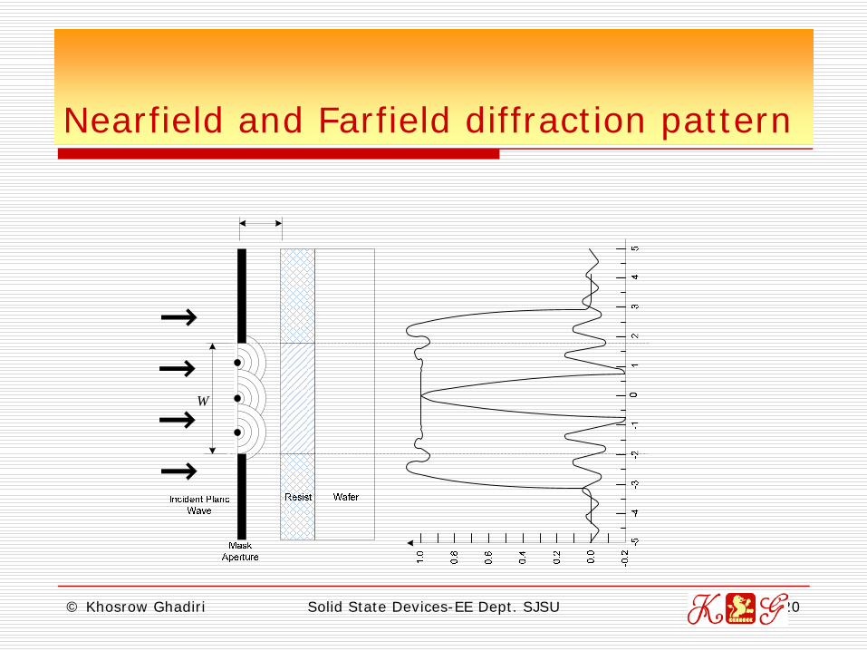
Nearfield and Farfield diffraction pattern
W
© Khosrow Ghadiri Solid State Devices-EE Dept. SJSU 21
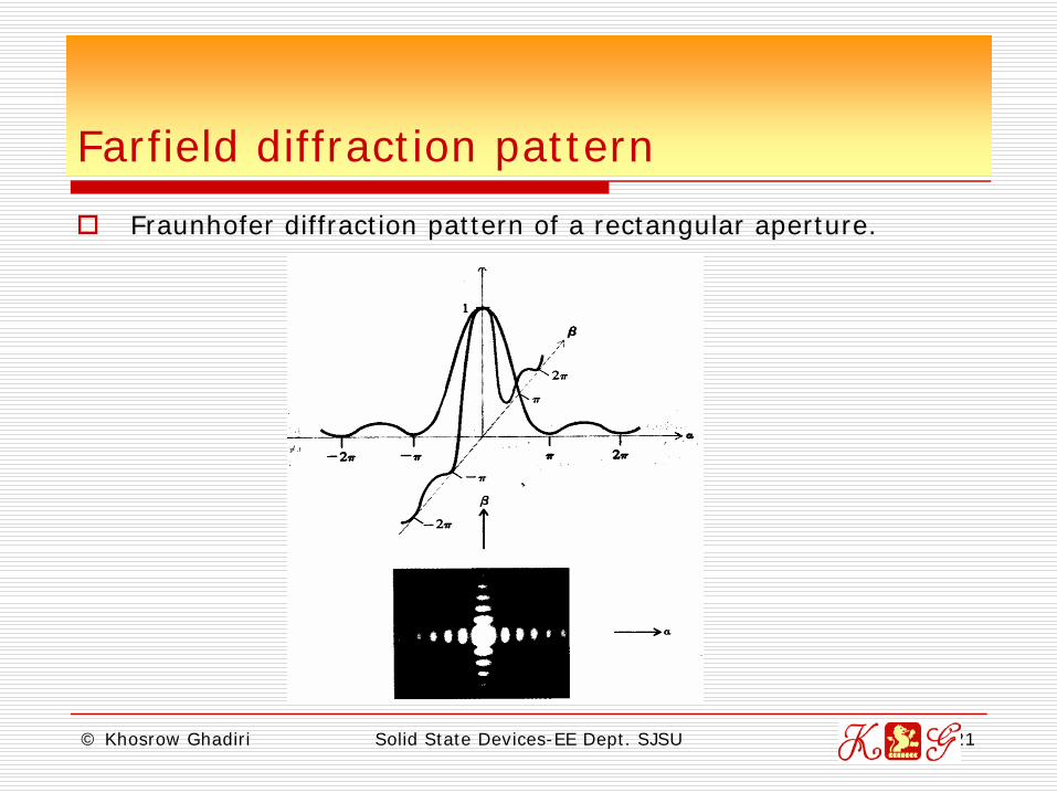
Farfield diffraction pattern
Fraunhofer diffraction pattern of a rectangular aperture.

© Khosrow Ghadiri Solid State Devices-EE Dept. SJSU 22
Farfield diffraction pattern
Fraunhofer diffraction pattern of a circular aperture.
© Khosrow Ghadiri Solid State Devices-EE Dept. SJSU 23
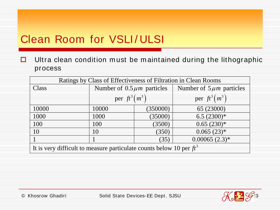
Clean Room for VSLI/ULSI
Ultra clean condition must be maintained during the lithographic process
Ratings by Class of Effectiveness of Filtration in Clean Rooms Class Number of 0.5 mμ particles
per ( )3 3ft m Number of 5 mμ particles
per ( )3 3ft m 10000 10000 (350000) 65 (23000) 1000 1000 (35000) 6.5 (2300)* 100 100 (3500) 0.65 (230)* 10 10 (350) 0.065 (23)* 1 1 (35) 0.00065 (2.3)* It is very difficult to measure particulate counts below 10 per 3ft
© Khosrow Ghadiri Solid State Devices-EE Dept. SJSU 24
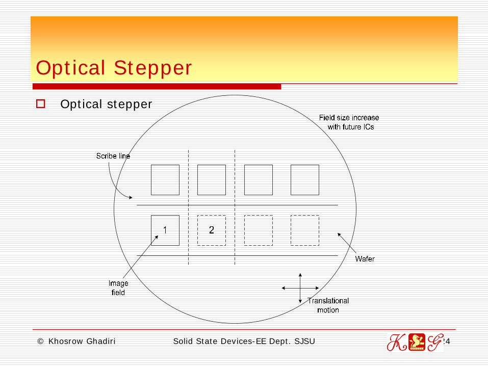
Optical Stepper
Optical stepper

© Khosrow Ghadiri Solid State Devices-EE Dept. SJSU 25
Step controlStep control
Box or crosson wafer
Cross or boxon mask
Composite patternafter alignment