printed wiring board technology infusion and supplier
TRANSCRIPT

National Aeronautics and Space Administration
www.nasa.govS a f e l y A c h i e v e A m a z i n g S c i e n c eT h r o u g h M i s s i o n S u c c e s s
S A F E T Y a n d M I S S I O N A S S U R A N C E D I R E C T O R A T E C o d e 3 0 0
Printed Wiring Board Technology Infusion and Supplier Capability Overview
Bhanu SoodCommodity Risk Assessment Engineer
Risk and Reliability BranchQuality and Reliability Division
NASA Goddard Space Flight CenterNASA Safety Center WebinarJune 12, 2018
Distribution statement: Approved for public release. S A F E T Y a n d M I S S I O N A S S U R A N C E D I R E C T O R AT E C o d e 3 0 0
Outline
• Printed circuit board technology • PCB quality assurance• Supplier capability study• New technology insertion/TRL• Risk based methods• Closure
2
S A F E T Y a n d M I S S I O N A S S U R A N C E D I R E C T O R AT E C o d e 3 0 0
Introduction
• In today’s compressed development cycles where rapid and cost-effective testing and analysis are key, a properly designed and executed quality assurance function (with appropriate reliability analysis) can enable products with robust design margins.
3
SOURCE: Industrial Laser Solutions. PCBShop.org
• If the mission conditions are not well understood or the reliability analysis and accelerated testing are not conducted right, cost and schedule impacts, along with unexpected failures will add risk to a Project development cycle.
S A F E T Y a n d M I S S I O N A S S U R A N C E D I R E C T O R AT E C o d e 3 0 0
• Printed circuit boards are the baseline in electronic packaging – they are the interconnection medium upon which electronic components are formed into electronic systems. – PCB materials are generally glass reinforced organic
polyimide (epoxy, BT, ceramic are also used).
• Classified on the basis of – Dielectrics used – Reinforcement– Circuit type – Component types– Board construction – Design complexity
Printed Circuit Boards and Classification
Examples of Bare PCBs
4
Populated PCBA

S A F E T Y a n d M I S S I O N A S S U R A N C E D I R E C T O R AT E C o d e 3 0 0
Polyimide PCBA Supply Chain*
Drill Bits
Glass Raw Materials(Silica, Limestone, Clay, Boric Acid)
Design and Coupon Data
Glass Fiber Production(Formation, Coating/Binders, Yarns)
E-Glass Plies/Fabrics
Polyimide Raw Materials(Petrochemical Derivatives)
Prepregs/Cores
Laminates
Solder Mask/Silk ScreenENIG/HASL/ENEPIG
/OSP/other Plating
Printed Circuit Board Panels w/Coupons
Copper Foil
Oxide CoatingsConsumables (e.g., etchants, cleaners)
Flame RetardantsFillers and Additives
AssemblyProcesses
5
Raw materials suppliers
Laminate suppliers
Board fabricators
Assembly houses
Active/Passive/Discrete Electronic parts, HW AOI and Inspections
Solder, flux, cleaning chemistries
ICT, Tests, Burn-in
* - Sood, Bhanu, and Michael Pecht. "Printed Circuit Board Laminates." Wiley Encyclopedia of Composites (2011).
S A F E T Y a n d M I S S I O N A S S U R A N C E D I R E C T O R AT E C o d e 3 0 0
Major Constituents of Laminates*Constituent Major function (s) Example material (s)
Reinforcement Provides mechanical strength and electrical properties Woven glass (E-grade) fiber
Coupling agent Bonds inorganic glass with organic resin and transfers stresses across the structure Organosilanes
Matrix Acts as a binder and load transferring agent Polyimide
Curing agent Enhances linear/cross polymerization in the resin Dicyandiamide (DICY), Phenol novolac (phenolic)
Flame retardant Reduces flammability of the laminate Halogenated (TBBPA), Halogen-free (Phosphorous compounds)
Fillers Reduces dissipatation (high frequency), thermal expansion and cost of the laminate
Silica,Aluminum hydroxide
Accelerators Increases reaction rate, reduces curing temperature, controls cross-link density
Imidazole,Organophosphine
* - Sood, Bhanu, and Michael Pecht. "Printed Circuit Board Laminates." Wiley Encyclopedia of Composites (2011).
6
S A F E T Y a n d M I S S I O N A S S U R A N C E D I R E C T O R AT E C o d e 3 0 0
Example: Glass Fabric Treatment*
1080 Style 2116 Style 7628 StyleFiber/resin interphase
delamination occurs due poor glass treatment.
Glass Weave Style
* - Sood, Bhanu, and Michael Pecht. "The effect of epoxy/glass interfaces on CAF failures in printed circuit boards." Microelectronics Reliability (2017).
Glass Weave Style Glass Weave Style
7 S A F E T Y a n d M I S S I O N A S S U R A N C E D I R E C T O R AT E C o d e 3 0 0 8
Bare PCB Suppliers*
* - “Challenges and Opportunities: State of the U.S. Bare Printed Circuit Board Industry” Crawford M. and Botwin B., IPC APEX Expo, February 11-16, 2017, San Diego CA. Reproduced with permission.

S A F E T Y a n d M I S S I O N A S S U R A N C E D I R E C T O R AT E C o d e 3 0 0 9
Support to U.S. Government Agencies*
* - “Challenges and Opportunities: State of the U.S. Bare Printed Circuit Board Industry” Crawford M. and Botwin B., IPC APEX Expo, February 11-16, 2017, San Diego CA. Reproduced with permission.
S A F E T Y a n d M I S S I O N A S S U R A N C E D I R E C T O R AT E C o d e 3 0 0 10
Bare PCB Supplier Capabilities*
* - “Challenges and Opportunities: State of the U.S. Bare Printed Circuit Board Industry” Crawford M. and Botwin B., IPC APEX Expo, February 11-16, 2017, San Diego CA. Reproduced with permission.
S A F E T Y a n d M I S S I O N A S S U R A N C E D I R E C T O R AT E C o d e 3 0 0 11
Material Supply Chain Disruptions*
* - “Challenges and Opportunities: State of the U.S. Bare Printed Circuit Board Industry” Crawford M. and Botwin B., IPC APEX Expo, February 11-16, 2017, San Diego CA. Reproduced with permission.
S A F E T Y a n d M I S S I O N A S S U R A N C E D I R E C T O R AT E C o d e 3 0 0
Factors Causing PCB Production Bottlenecks*
* - “Challenges and Opportunities: State of the U.S. Bare Printed Circuit Board Industry” Crawford M. and Botwin B., IPC APEX Expo, February 11-16, 2017, San Diego CA. Reproduced with permission.
12

S A F E T Y a n d M I S S I O N A S S U R A N C E D I R E C T O R AT E C o d e 3 0 0
• In a vast majority of cases, NASA uses IPC standards (e.g., IPC-6012, 6013)– IPC-6012 for rigid, IPC-6013 flex, IPC-6018 high speed etc..
• Inspection include:– Microsection evaluation (coupons)– Surface finish evaluation (coupons)
• Test include:– External visual examination– Electrical continuity and isolation– Solderability (not 100% cases)– Cleanliness
PCB Quality
13
• In some cases MIL, ESA or “in-house” standards are applied.
XRF Spectrum
PTH in Crosssection
S A F E T Y a n d M I S S I O N A S S U R A N C E D I R E C T O R AT E C o d e 3 0 0
Significance of Board Requirements• The requirements and coupons are a “front door”.• Examples:
– Internal Annular Ring:• Egregious violations indicate there may have been a serious problem in
development of the board (layup or lamination).• Other NCs don’t indicate any risk at all (example: application of IPC-
6012 Rev B. v/s IPC-6012 Rev. D)– Negative etchback v/s positive etchback:
• Modern cleaning processes and flight experience result in equal reliability with both etchback conditions or no etchback.
– Wicking of copper:• Requirements are conservative based on broad statistics.• A basic analysis of the board layout can indicate directly if there is risk or
not, regardless of requirements violations.
14
S A F E T Y a n d M I S S I O N A S S U R A N C E D I R E C T O R AT E C o d e 3 0 0
PCB Supplier Evaluation Study
15 S A F E T Y a n d M I S S I O N A S S U R A N C E D I R E C T O R AT E C o d e 3 0 0
Study Objective
– Evaluate a subset of GSFC PCB suppliers (direct or indirect) and corresponding PCB coupon microsection testing data.
– Develop a methodology for data generation and collection to provide trend analysis • Identifies/predicts violation of a process limit criteria (in case
of an egregious NC). – Provide analysis for severity categories of the nonconformance.– Provide recommendations to the suppliers (i.e. supplier quality
engineering, continuous process monitoring, quality metrics definition).
16

S A F E T Y a n d M I S S I O N A S S U R A N C E D I R E C T O R AT E C o d e 3 0 0
Microsectioning• Suppliers perform
microsectioning and inspect per specifications.
17
• Secondary GSFC independent microsection analysis yielded 20-30% inspection rejects, caused by:– Screening escapes:
• Test sample quality not consistent• Supplier microsection process, inadequate coupons
– Requirement interpretations– Requirements flow-down issues
• Alternative specifications (MIL, ECSS)• Buying heritage and off-the-shelf designs
IPC - PCB Multi-Issue Microsection Wall Poster*
* - https://blog.ipc.org/2010/11/22/pcb-multi-issue-microsection-wall-poster/
S A F E T Y a n d M I S S I O N A S S U R A N C E D I R E C T O R AT E C o d e 3 0 0
Requirements, Nonconformance, Data Generation and Collection• Present study evaluates only the microsections performed by GSFC.
– PCB coupon microsection evaluation in accordance to IPC Standard (IPC-6018B Class 3, IPC-6012C Class 3/A).
– Coupon evaluation reports were generated, identified non-conformances.
• All PCB coupon testing results from all GSFC suppliers were recorded for the past 3 years (from 2015 – present) – Data include nonconformance and conformances in accordance
with IPC Standards.– Total number of data points are approximately 882 jobs.– Each job has number of nonconformance with different severity.
18
S A F E T Y a n d M I S S I O N A S S U R A N C E D I R E C T O R AT E C o d e 3 0 0
Study Methodology
• Since 2015, received and analyzed 882 PCB coupon submissions from PCB suppliers.
• Top ten suppliers sent 638 submissions.• Total nonconformance observed: 260
• For each supplier, analyzed nonconformance (s)– Identify severity trend across top 10 GSFC suppliers by analyzing
submission rate and nonconformance spread.– Classifying and analyzing top 5 severity categories.
19 S A F E T Y a n d M I S S I O N A S S U R A N C E D I R E C T O R AT E C o d e 3 0 0
Data Analysis –Submission and Nonconformance for Supplier
0
0.05
0.1
0.15
0.2
0.25
0.3
1 2 3 4 5 6 7 8 9 10
Frac
tion
Top 10 SuppliersSupplier's submission rate Nonconformance spread
20
Supplier submission rate = total submission by individual supplier
total submission by all supplier
Nonconformance spread = total nonconformance by individual supplier
total nonconformance by all suppliers
638 submissions

S A F E T Y a n d M I S S I O N A S S U R A N C E D I R E C T O R AT E C o d e 3 0 0
Classification and Analysis - Top 5 NonconformancesTwenty one distinct conformances observed among the ten suppliers
Com
mon
Non
conf
orm
ance
s fro
m su
pplie
rs
PCB Suppliers1 2 3 4 5 6 7 8 9 10A F E K A N E E A EB G D F F O P A F FC H B L D F C D S TD A I J J E D F D UE D J A M P Q R P R
21
NC Nonconformance StandardA Inner layer separations/inclusions IPC 6012B Class 3/AB Electroless Ni less than 118microinches IPC 6012B Class 3/AC Plating voids IPC 6012DSD Separation/inclusions between plating layers IPC 6012B Class 3/AE Copper wicking in excess of 2.0mil IPC 6012B Class 3/AF Internal annular ring less than 2.0mil IPC 6012B Class 3/AG Internal annular ring less than 5.0mil (drwg. note) IPC 6012B Class 3/AH External annular ring less than 5.0mil IPC 6012B Class 3/AI Immersion gold less than 3.0micro inches IPC 6012DS
JElectroless nickel and immersion gold platingthickness < 118micro inches (Ni) and 2micro IPC 6012B Class 3/A
K Blind via plating thickness less than 0.8mil IPC 6012B Class 3/AL Resin recession greather than 3mil IPC 6012B Class 3/AM Solid copper micro via voids in excess of 33% 8252313CN Laminate delamination IPC 6012B Class 3/AO laminate cracks IPC 6012C Class 3/AP Etchback less than 0.2mil IPC 6012B Class 3/AQ Immersion gold plating thickness in excess of 6mil IPC 6012C Class 3/AR Copper plating thickness less than 1.0mil IPC 6012B Class 3/AS Laminate crack greater than 3.0mil IPC 6012B Class 3/AT Dielectric thickness less than 3.0mil min IPC 6012B Class 3/AU Laminate void greater than 3.0mil IPC 6012B Class 3/A
S A F E T Y a n d M I S S I O N A S S U R A N C E D I R E C T O R AT E C o d e 3 0 0
Analyzing Top 5 Severities of Supplier’s Nonconformance
• Observations show the nonconformances with the most occurrences (7 out of 10 Suppliers) are D and F.
• Investigated the contributors to implement techniques which may eliminate theses nonconformances from at least 7 suppliers.
(A) Inner layer separations/inclusions
(D) Separation/inclusions between plating layers
(E) Copper wicking in excess of 2.0 mil
(F) Internal annular ring less than 2.0 mil
(J) ENIG is less than the minimum requirements
22
* - “Challenges and Opportunities: State of the U.S. Bare Printed Circuit Board Industry” Crawford M. and Botwin B., IPC APEX Expo, February 11-16, 2017, San Diego CA. Reproduced with permission.
S A F E T Y a n d M I S S I O N A S S U R A N C E D I R E C T O R AT E C o d e 3 0 0
Inner Layer Separations or Inclusions
• Separation of inner-layer foil and the plated through hole barrel.
• Inclusion - contaminant material that is present in an area where it is not expected.
23
1. IPC-6012 – Qualification and Performance Specification for Rigid Printed Boards.2. Swirbel, Tom, Adolph Naujoks, and Mike Watkins. "Electrical design and simulation of high density printed circuit
boards." IEEE transactions on advanced packaging 22.3 (1999): 416-423.
Risk: intermittent electrical open or complete open after board is
subjected to thermal excursions (reflow, wave soldering or rework)
S A F E T Y a n d M I S S I O N A S S U R A N C E D I R E C T O R AT E C o d e 3 0 0
Contributors• Improper lamination press or cure cycles
whether it be pressure, time, temperature.
• Others include inadequate coverage of inner layer oxide, moisture not completely removed in pre-lamination bake cycle.
• Bad batch of prepreg and or laminate.
• Post-electroless copper cleaning residues, contaminated pretreatment prior to electrolytic plating, or an out-of-control electrolytic copper process.
Resolution• Consistency in drilling processes.• Reduce the resin content in the
stack up.• Good desmear, with adequate
texture.• Provide adequate copper border
for support and resin venting
24
Inner Layer Separations or Inclusions

S A F E T Y a n d M I S S I O N A S S U R A N C E D I R E C T O R AT E C o d e 3 0 0
Separation or Inclusions Between Plating Layers
Plating separation -The separation between a plating layer and foil.
25
1. IPC-6012 – Qualification and Performance Specification for Rigid Printed Boards.2. Yung, Edward K., Lubomyr T. Romankiw, and Richard C. Alkire. "Plating of Copper into Through Holes and
Vias." Journal of the Electrochemical Society 136.1 (1989): 206-215.
Risk: intermittent electrical open or complete opens due to mechanical or thermal stresses.
S A F E T Y a n d M I S S I O N A S S U R A N C E D I R E C T O R AT E C o d e 3 0 0
Contributors• Incomplete wrap plating• Overly-aggressive cleaning
process• Insufficient cleaning
Resolution• Adjust plating parameters• Optimize cleaning processes
26
Separation or Inclusions Between Plating Layers
S A F E T Y a n d M I S S I O N A S S U R A N C E D I R E C T O R AT E C o d e 3 0 0
Copper Wicking in Excess of 2.0 mil
The extension of copper from a PTH along the glass fiber fabric.
27
1. Sood, Bhanu, and Michael Pecht. "Printed Circuit Board Laminates." Wiley Encyclopedia of Composites (2011).2. Tummala, Rao R., Eugene J. Rymaszewski, and Y. C. Lee. "Microelectronics packaging handbook." (1989): 241-
242.3. IPC-6012 – Qualification and Performance Specification for Rigid Printed Boards.
Risk: intermittent electrical shorts or complete shorts due to bias driven migration of copper towards non-
common conductors.
S A F E T Y a n d M I S S I O N A S S U R A N C E D I R E C T O R AT E C o d e 3 0 0
Contributors• Dull drill bits or broken drill bits
that causes a crack in the laminate.
• Incompatible laminate material• Insufficient glass etch.• Poor glass to organic adhesion.
Resolution• Optimize desmear parameters• Improve drilling operation (feed
and speed).• Ensure sufficient resin wet-out of
glass fibers (siloxane treatment).
28
Copper Wicking in Excess of 2.0 mil

S A F E T Y a n d M I S S I O N A S S U R A N C E D I R E C T O R AT E C o d e 3 0 0
Internal Annular Ring Less Than 2.0 mil
This occurs, when the inner layer copper pad (measured from the hole wall plating to its outer most length) is less than 2 mils.
29
1. Sood, Bhanu, and Sindjui, N. "A Comparison of Registration Errors Amongst Suppliers of Printed Circuit Boards“, Proceedings, IPC APEX Expo (2018).
2. IPC-6012 – Qualification and Performance Specification for Rigid Printed Boards.
Risk: inner layer breakouts after the board is subjected to thermal
excursions (reflow, wave soldering or rework) leading to intermittent
electrical or complete open behavior.
S A F E T Y a n d M I S S I O N A S S U R A N C E D I R E C T O R AT E C o d e 3 0 0
Contributors• Drilled-hole pattern not matching
the lands on the internal layers (Misregistration).
• Lamination process.• Prelamination treatments that
involve scrubbing or bending may stretch the thin laminate, which will then shrink after it is etched and baked dry.
• Application of specification or drawing notes.
Resolution• Better material selection of
laminate, improved cleanliness, and reduction in the amount of volatiles.
• Confirm whether or not it is operator error.
• Update drawing notes to bring the notes in line with current industry maturity levels.
30
Internal Annular Ring Less Than 2.0 mil
S A F E T Y a n d M I S S I O N A S S U R A N C E D I R E C T O R AT E C o d e 3 0 0
ENIG (Au or Ni) Less than the Minimum
Electroless nickel and/or immersion gold plating thickness (ENIG) is less than the minimum requirements (118 micro-inches for Ni and 2 micro-inches for Au).
31
XRF Spectrum
1. Johal, Kuldip, and Jerry Brewer. "Are you in control of your electroless nickel/immersion gold process?." Proc. Of IPC Works. No. S03-3. 2000.
2. Meng, Chong Kam, Tamil Selvy Selvamuniandy, and Charan Gurumurthy. "Discoloration related failure mechanism and its root cause in Electroless Nickel Immersion Gold (ENIG) Pad metallurgical surface finish." Physical and Failure Analysis of Integrated Circuits, 2004. IPFA 2004. Proceedings of the 11th International Symposium on the. IEEE, 2004.
3. IPC-4552 – Specification for Electroless Nickel/Immersion Gold (ENIG) Plating for Printed Circuit Boards
Risk: (1) solderability and, (2) excessive dissolution of copper into
the bulk solder (forming brittle intermetallic) when nickel is thin.
S A F E T Y a n d M I S S I O N A S S U R A N C E D I R E C T O R AT E C o d e 3 0 0
ENIG Less than Minimum
Contributors• Improper cleaning of surfaces.• Improper or inadequate rinsing.• Bath parameters not being
followed (pH and chemical).• Bath temperature too low.• Copper surface not clean of oil or
inhibiting film.
Resolution• Re-clean copper using chemical
cleaners or mechanical• scrubbing Institute micro-etch step
to improve cleaning• Improve rinsing( Check flow,
agitation and water quality)• Raise temperature per supplier
specifications• Readjust to supplier operational
parameters
32

S A F E T Y a n d M I S S I O N A S S U R A N C E D I R E C T O R AT E C o d e 3 0 0
Summary of Supplier Study
• The test data is analyzed using statistical method to provide trend analysis for all suppliers. – Root cause(s) and key contributors are identified.– Mitigation plan is included for the root cause of nonconformance.
• Provide recommendations to the supplier’s process, identification and prediction of nonconforming process limit criterion, and to improve test standards.
• New technologies (example: smaller annular rings, via-in-pads, thinner laminates or newer plating) are implemented on the basis of supplier maturity and reported NCs.
33 S A F E T Y a n d M I S S I O N A S S U R A N C E D I R E C T O R AT E C o d e 3 0 0
New technology Implementation: Technology Readiness Levels
34
S A F E T Y a n d M I S S I O N A S S U R A N C E D I R E C T O R AT E C o d e 3 0 0
“TRLs are a set of metrics that enable the assessment of the maturity of a particular technology and the consistent comparison of the maturity between different types of technology in the context of a specific application, implementation, and operational environment.”
Technology Readiness Levels
Once TLR6 isdemonstrated, the riskassociated with the newtechnology is roughlyequivalent to the risk of anew design that employsstandard engineeringpractice and is boundedby previouslyimplemented groundbased systems.
35 S A F E T Y a n d M I S S I O N A S S U R A N C E D I R E C T O R AT E C o d e 3 0 0
• A new technology can be at a different TRL depending on the requirements.
• Not all new designs are new technology
– Some may be considered “standard engineering” (e.g., a new primary structure based on existing design and fabrication processes)
TRL Implementation – Considerations
36
• The configuration for TRL verification occurs at the lowest level of integration that exhibits the new performance/functionality.
• The “weakest link” approach is used to determine the TRL of a subsystem
– There can be cases where a subsystem’s TRL is lower than that of all of its elements (e.g., a new architecture that is used to provide new performance, but employs all “heritage parts”).
S A F E T Y a n d M I S S I O N A S S U R A N C E D I R E C T O R AT E C o d e 3 0 0
Risk Based Technology Evaluation and Insertion
37 S A F E T Y a n d M I S S I O N A S S U R A N C E D I R E C T O R AT E C o d e 3 0 0
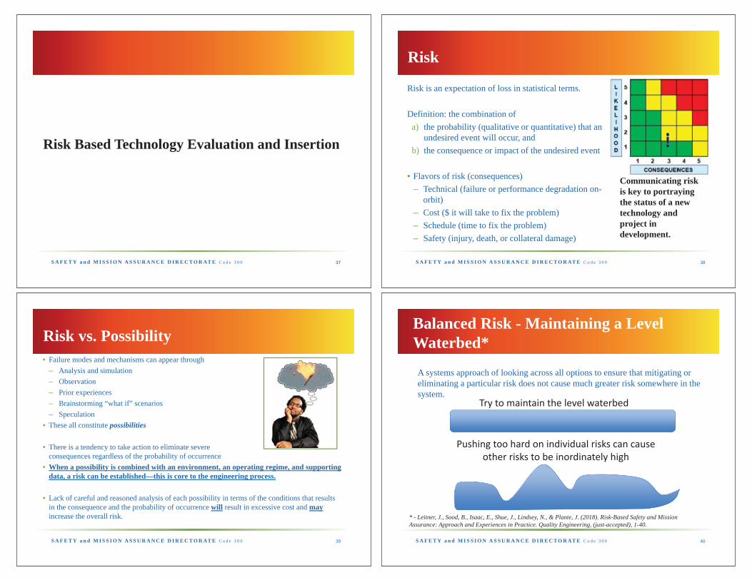
Risk is an expectation of loss in statistical terms.
Definition: the combination of a) the probability (qualitative or quantitative) that an
undesired event will occur, andb) the consequence or impact of the undesired event
• Flavors of risk (consequences)– Technical (failure or performance degradation on-
orbit)– Cost ($ it will take to fix the problem)– Schedule (time to fix the problem)– Safety (injury, death, or collateral damage)
Risk
Communicating risk is key to portraying the status of a new technology and project in development.
38
S A F E T Y a n d M I S S I O N A S S U R A N C E D I R E C T O R AT E C o d e 3 0 0
• Failure modes and mechanisms can appear through– Analysis and simulation– Observation– Prior experiences – Brainstorming “what if” scenarios– Speculation
• These all constitute possibilities
• There is a tendency to take action to eliminate severe consequences regardless of the probability of occurrence
• When a possibility is combined with an environment, an operating regime, and supporting data, a risk can be established—this is core to the engineering process.
• Lack of careful and reasoned analysis of each possibility in terms of the conditions that results in the consequence and the probability of occurrence will result in excessive cost and mayincrease the overall risk.
Risk vs. Possibility
39 S A F E T Y a n d M I S S I O N A S S U R A N C E D I R E C T O R AT E C o d e 3 0 0
Balanced Risk - Maintaining a Level Waterbed*
A systems approach of looking across all options to ensure that mitigating or eliminating a particular risk does not cause much greater risk somewhere in the system.
40
Pushing too hard on individual risks can causeother risks to be inordinately high
Try to maintain the level waterbed
* - Leitner, J., Sood, B., Isaac, E., Shue, J., Lindsey, N., & Plante, J. (2018). Risk-Based Safety and Mission Assurance: Approach and Experiences in Practice. Quality Engineering, (just-accepted), 1-40.

S A F E T Y a n d M I S S I O N A S S U R A N C E D I R E C T O R AT E C o d e 3 0 0
Impact of Non-conformances
• Bare boards cost $$ and build schedules – expensive!!
• But failures are even more expensive!• Test sample nonconformance is not
the same as PCB failure.• Risk-based decisions are used for
disposition of non-conformances.• Non-conformances may have little to
no impact per application.• Began to explore origins and merit of
requirements (more later).
41 S A F E T Y a n d M I S S I O N A S S U R A N C E D I R E C T O R AT E C o d e 3 0 0
• Traceable PCB test coupons (designed per specs. such as IPC-2221B) are submitted to GSFC or to a GSFC-assessed laboratory.
• Reports that indicate nonconformance are dispositioned by risk assessment performed prior to refabricating or populating the PCB.
– If risk assessment indicates elevated risk due to the nonconformance, then use is dispositioned by MRB.
• Risk assessment process eliminates waste and saves money and schedule, lowers overall risk for the project.
• The process reduces the need for repeated attempts to refabricate.
Risk Assessment
42
S A F E T Y a n d M I S S I O N A S S U R A N C E D I R E C T O R AT E C o d e 3 0 0
• Risk-based new technology assessment centered around understanding all sides of risk.
• Lessons learned are at the core of the methodology • This approach is effective at saving cost and schedule resources.• Enables any project to operate at the lowest possible risk posture given its
particular resource constraints.
Summary
43
Lessons learned from non-
conformance data
TRL Evaluation Supplier capability and assessment
Risk Assessment for new technology
insertion
S A F E T Y a n d M I S S I O N A S S U R A N C E D I R E C T O R AT E C o d e 3 0 0
NASA Workmanship Program
Acknowledgements
44
NASA Office of Safety and Mission Assurance,
Quality Program
NASA Goddard Risk and Reliability Branch

S A F E T Y a n d M I S S I O N A S S U R A N C E D I R E C T O R AT E C o d e 3 0 0 45
Bhanu SoodCommodity Risk Assessment Engineer
Risk and Reliability BranchQuality and Reliability Division
NASA Goddard Space Flight Center
+1 (301) 286 [email protected]
S A F E T Y a n d M I S S I O N A S S U R A N C E D I R E C T O R AT E C o d e 3 0 0
Backup Slides
46
S A F E T Y a n d M I S S I O N A S S U R A N C E D I R E C T O R AT E C o d e 3 0 0
TRL Definition and Decomposition by Factor*
TRL Definition from NPR7123.1e
Completion Criteria fromNPR 7123.1e
MissionReq.
Performance/ Function Fidelity of Analysis Fidelity of Build Level of Integration Environment Verification
4 Component and/orbread board validatedin laboratoryenvironment
Documented testperformancedemonstrating agreementwith analyticalpredictions. Documenteddefinition of relevantenvironment.
Genericclass ofmissions
Basic functionality/performancedemonstrated
Medium fidelity: to predict keyperformance parameters and lifelimiting factors as a function ofrelevant environments
Low fidelity: breadboard
Component/Assembly
Tested in laboratory forcritical environments
Relevant environmentsidentified. Life limitingmechanisms identified.
5 Component and/orbrass board validated inrelevant environment
Documented testperformancedemonstrating agreementwith analyticalpredictions. Documenteddefinition of scalingrequirements.
Generic orspecificclass ofmissions
Basic functionality/performance maintained
Medium fidelity: to predict keyperformance parameters and lifelimiting factors as a function ofrelevant environments
Medium fidelity:brass board withrealistic supportelements
Component/Assembly
Tested in relevantenvironmentsCharacterize physics oflife limiting mechanismsand failure modes.
6 System/ subsystemmodel or prototypedemonstrated in arelevant environment
Documented testperformancedemonstrating agreementwith analytical predictions
Specificmission
Required functionality/performancedemonstrated
Medium fidelity: to predict keyperformance parameters and lifelimiting factors as a function ofoperational environments
High fidelity:prototype thataddresses all criticalscaling issues
Subsystem/ System Tested in relevantenvironments. Verify bytest that the technology isresilient to the effects oflife limiting mechanisms
7 System prototypedemonstration in anoperationalenvironment
Documented testperformancedemonstrating agreementwith analytical predictions
Tech nologydemonstrationmission
Required functionality/performancedemonstrated
High fidelity: to predict keyperformance parameters and lifelimiting factors as a function ofoperational environments
High Fidelity:prototype orengineering unit thataddresses all criticalscaling issues
Subsystem/System Tested in actualoperational environment
8 Actual systemcompleted and “flightqualified” through testand demonstration
Documented testperformance verifyingrequirements andanalytical predictions
Specificmission
Required functionality/performancedemonstrated
High fidelity: to predict keyperformance parameters and lifelimiting factors as a function ofoperational environments
Final product:
Flight unit;
Life test unit for lifelimited items*
System Tested in projectenvironmental verificationprogram.
Completed life tests.
9 Actual system flightproven throughsuccessful missionoperations
Documented missionoperational resultsverifying requirements
Specificmission
Required functionality/performancedemonstrated
High fidelity: to predict keyperformance parameters and lifelimiting factors as a function ofoperational environments
Final product:
Flight unit
System Operated in actualoperational environment
47
NASA Systems Engineering Processes and Requirements (NPR) 7123.1B (Table 3.1.3-1)S A F E T Y a n d M I S S I O N A S S U R A N C E D I R E C T O R AT E C o d e 3 0 0
Fidelity of Build
Table 3.1.6 1: Fidelity of Build
Unit PurposePerformance/
FunctionForm and Fit/ Scaling
EnvironmentalRequirements
Pedigree
New
Techno
logy
Developm
ent
Breadboard Proof of concept for a potential design Demonstrateperformance/ function
Not required, e.g. laid outflat on lab table
Tested in a laboratoryenvironment
NA
Brassboard Demonstrate feasibility of form and fit,environments
Demonstrateperformance/ function
Approximate (not flat)with scaling factorsunderstood
Designed to meet relevantenvironmentalrequirements
NA
Prototype Representative design; pathfinder; demonstrator Tested to meetperformance/ functionrequirements
Representative withscaling factors understood
Tested to meet relevantenvironmentalrequirements
NA, but may bepartial or full
Engine
eringDe
velopm
ent
EngineeringUnit
Finalize detailed design Tested to meetperformance/ functionrequirements
Exact as known at time ofbuild
Tested to meet relevantenvironmentalrequirements
NA, but may bepartial or full
QualificationUnit
Qualify design Tested to meetperformance/ functionrequirements
Exact as known at time ofbuild
Tested to meet flightqualificationenvironmentalrequirements
Full
Flight Unit Final Product Tested to meetperformance/ functionrequirements
Exact Tested to meet flightqualificationenvironmentalrequirements
Full
Flight Spare Final Product Tested to meetperformance/ functionrequirements
Exact Tested to meet flightqualificationenvironmentalrequirements
Full
48

S A F E T Y a n d M I S S I O N A S S U R A N C E D I R E C T O R AT E C o d e 3 0 0
At the Subsystem level• Specific mission (and specific mission risk class) • Required functionality/ performance demonstrated• Medium fidelity: to predict key performance parameters and life
limiting factors as a function of operational environments• High fidelity: prototype that addresses all critical scaling issues• Subsystem tested in relevant environments.
– Verify by test that the technology is resilient to the effects of life-limiting mechanisms
– Note, “relevant environment” is a subset of the operational environment and specifically focuses on “stressing” the new technology
TRL 6
49 S A F E T Y a n d M I S S I O N A S S U R A N C E D I R E C T O R AT E C o d e 3 0 0
• Class A: Lowest risk posture by design – Failure would have extreme consequences to public safety or high priority national science objectives. – In some cases, the extreme complexity and magnitude of development will result in a system launching with
many low to medium risks based on problems and anomalies that could not be completely resolved under cost and schedule constraints.
– Examples: HST and JWST• Class B: Low risk posture
– Represents a high priority National asset whose loss would constitute a high impact to public safety or national science objectives
– Examples: GOES-R, TDRS-K/L/M, MAVEN, JPSS, and OSIRIS-REX• Class C: Moderate risk posture
– Represents an instrument or spacecraft whose loss would result in a loss or delay of some key nationalscience objectives.
– Examples: LRO, MMS, TESS, and ICON• Class D: Cost/schedule are equal or greater considerations compared to mission success risks
– Technical risk is medium by design (may be dominated by yellow risks). – Many credible mission failure mechanisms may exist. A failure to meet Level 1 requirements prior to minimum
lifetime would be treated as a mishap.– Examples: LADEE, IRIS, NICER, and DSCOVR
Risk Classification (NPR 7120.5 Projects)
50