probe-based ultrahigh-density storage technology
TRANSCRIPT

Probe-basedultrahigh-densitystoragetechnology
A. PantaziA. Sebastian
T. A. AntonakopoulosP. Bachtold
A. R. BonaccioJ. Bonan
G. CherubiniM. Despont
R. A. DiPietroU. Drechsler
U. DurigB. Gotsmann
W. HaberleC. HagleitnerJ. L. Hedrick
D. JubinA. Knoll
M. A. LantzJ. Pentarakis
H. PozidisR. C. Pratt
H. RothuizenR. Stutz
M. VarsamouD. WiesmannE. Eleftheriou
Ultrahigh storage densities can be achieved by using athermomechanical scanning-probe-based data-storage approach towrite, read back, and erase data in very thin polymer films. Highdata rates are achieved by parallel operation of large two-dimensional arrays of cantilevers that can be batch fabricated bysilicon-surface micromachining techniques. The very high precisionrequired to navigate the storage medium relative to the array ofprobes is achieved by microelectromechanical system (MEMS)-based x and y actuators. The ultrahigh storage densities offered byprobe-storage devices pose a significant challenge in terms of bothcontrol design for nanoscale positioning and read-channel designfor reliable signal detection. Moreover, the high parallelismnecessitates new dataflow architectures to ensure high performanceand reliability of the system. In this paper, we present a small-scaleprototype system of a storage device that we built based onscanning-probe technology. Experimental results of multiplesectors, recorded using multiple levers at 840 Gb/in2 and read backwithout errors, demonstrate the functionality of the prototypesystem. This is the first time a scanning-probe recording technologyhas reached this level of technical maturity, demonstrating the jointoperation of all building blocks of a storage device.
Introduction
Today’s wide variety of data-storage applications creates
an increasing demand for high-capacity, fast-access, and
low-power memory devices. The areal densities of
conventional storage technologies will eventually reach
fundamental physical limits, such as those due to the
superparamagnetic effect in magnetic storage and the
scaling limits imposed by lithography in flash memories.
Therefore, new technologies are under investigation that
could potentially address the future needs of data-storage
applications.
Probe-based data-storage devices [1–6] are being
considered as ultrahigh-density and small-form-factor
alternatives to conventional data-storage devices such as
the microdrive and flash memory. Probe storage relies on
nanometer-sharp tips, similar to the ones used in atomic
force microscopy (AFM) and scanning tunneling
microscopy (STM) [7, 8], for manipulating the structure
or changing the properties of materials down to the
atomic scale. The use of such technologies allows
densities that are far beyond 1 Tb/in2 to be achieved.
Different approaches involving materials and recording
mechanisms have been investigated, such as the phase-
change approach for storing information using
amorphous-crystalline transitions in a phase-change
medium [9, 10], the magnetic probe-based approach in
which a magnetic storage medium is used and writing is
achieved magnetically by means of an array of probe tips
[11], and the ferroelectric approach in which information
is stored using ferroelectric domains [12].
This paper focuses on a probe-storage prototype that
exploits the thermomechanical method for storing and
retrieving data encoded as nanometer-scale indentations
in thin polymer films [5, 6]. Thermomechanical writing
was originally investigated in [13]. Recently, experimental
results using single probes have shown that with the
thermomechanical write/read process, data can be
recorded at a density of 641 Gb/in2 and read back with
�Copyright 2008 by International Business Machines Corporation. Copying in printed form for private use is permitted without payment of royalty provided that (1) eachreproduction is done without alteration and (2) the Journal reference and IBM copyright notice are included on the first page. The title and abstract, but no other portions, of thispaper may be copied by any means or distributed royalty free without further permission by computer-based and other information-service systems. Permission to republish any other
portion of this paper must be obtained from the Editor.
IBM J. RES. & DEV. VOL. 52 NO. 4/5 JULY/SEPTEMBER 2008 A. PANTAZI ET AL.
493
0018-8646/08/$5.00 ª 2008 IBM
raw error rates better than 10�4 prior to error-correction
coding [14]. Moreover, using advanced polymer media
and the same recording method, a feasibility study has
shown that densities of 4 Tb/in2 can be achieved [15].
Single probes are relatively slow in writing and
retrieving data compared to conventional techniques.
High data rates are possible by operating large arrays of
probes in parallel, with each probe performing read,
write, and erase operations on an individual storage field.
A first large two-dimensional (2D) array of 1,024
(32 3 32) cantilevers with integrated tips and sensors has
been successfully fabricated using silicon micromachining
techniques [16]. More recently, a new interconnect
technology for integrating the cantilever array with the
CMOS (complementary metal-oxide semiconductor)
analog front-end (AFE) chip has been developed [17]. In
this approach, the cantilever array is transferred and
interconnected to its CMOS AFE counterpart chip on a
full wafer-to-wafer basis, thereby overcoming the
challenge of connectivity to the driving electronics that is
encountered in the parallel operation of large cantilever
arrays.
In probe systems, the rotating-disk and single-head-
per-surface paradigm of hard-disk drives has been
abandoned in favor of microelectromechanical system
(MEMS)-based x and y actuators that position the
storage medium relative to the array of probe tips for
parallel write and read operations [18]. Typical actuation
distances are on the order of 100 lm. Moreover, in
addition to x and y actuators, positioning sensors are
required with a dynamic range of approximately 100 lmand displacement resolution of less than approximately
1 nm.
We have built a small-scale prototype storage system
based on arrays of scanning probes with complete servo-
navigation and parallel write and read functionality, and
we have demonstrated multiple-sector writing and
reading with eight probes in parallel at a record areal
density of 840 Gb/in2 and a raw bit error rate of
approximately 10�4 prior to error-correction coding. This
is the first time a scanning-probe recording technology
has reached this high level of technical maturity,
demonstrating the joint operation of all building blocks
of a storage device based on local-probe techniques. The
storage system encompasses 1) a MEMS assembly
comprising a cantilever array chip and a microscanner
carrying the storage medium, 2) an integrated analog
CMOS front-end chip driving the cantilever array, 3) a
novel poly-aryl-ether-ketone (PAEK)-based ultrahigh-
temperature polymer used as storage medium, and 4) a
new navigation system based on medium-derived
positioning information that achieves an ultrahigh
positioning resolution during reading and writing, as well
as 5) a servo controller for subnanometer positioning
during device formatting.
The remainder of this paper is organized as follows.
First, we describe the thermomechanical probe-storage
system, along with the primary challenges. A description
of the components of the MEMS storage device is then
given. Next, we discuss the system aspects of the storage
system. Experimental validation of the prototype
operation with a sector write/read demonstration is also
presented.
Thermomechanical probe-storage systemIn thermomechanical probe-based storage, information is
stored as sequences of indentations written on thin
polymer films using a 2D array of AFM cantilevers. The
presence or the absence of indentations corresponds to
logical 1s or 0s, respectively. Each cantilever performs
read, write, and erase operations in an individual storage
field with an area on the order of 100 lm 3 100 lm. The
tip–medium spacing is controlled globally, and the write
and read operations depend on mechanical x and y
scanning of the storage medium. High data rates are
possible by parallel operation of all or a subset of the
cantilevers.
Thermomechanical writing is performed by applying
an electrostatic force through the cantilever to the
polymer layer and simultaneously softening the polymer
layer by local heating. A heater integrated into the
cantilever directly above the tip is heated to a relatively
high temperature of about 4008C. The heat is transported
from the heater through the tip and into the polymer
medium under the tip apex [19]. For readback sensing, a
second heater placed beside the tip is heated to a
temperature in the range of 150–3008C. The principle of
thermal sensing exploits the fact that the thermal
conductance between the resistive heater and the storage
substrate changes as a function of the distance between
them [20]. The medium between the resistive heater and
the storage substrate, which in our case is air, transports
heat from the cantilever to the substrate. When the
distance between the cantilever and the substrate
decreases as the tip moves into an indentation, the heat
transport through the air becomes more efficient,
resulting in a change of the cantilever temperature.
Because the electrical resistance of the heater depends on
its temperature, the value of its resistance decreases when
the tip moves into an indentation. Under typical
operating conditions, the sensitivity of thermomechanical
sensing, determined by the relative variation of the heater
resistance DR/R, is approximately 10�4 for a distance
change of 1 nm. The speed of this thermomechanical
reading process is limited by the thermal time constant of
the heater, which is on the order of a few microseconds.
As mentioned above, one solution to achieve competitive
A. PANTAZI ET AL. IBM J. RES. & DEV. VOL. 52 NO. 4/5 JULY/SEPTEMBER 2008
494

data rates is to simultaneously access all or a large subset
of the cantilevers in the 2D array.
An important component of the probe-based storage
system is the miniaturized scanner with x and y motion
range that is on the order of the pitch between the
cantilevers in the array. To generate information about
the position of the microscanner, two pairs of thermal
position sensors are included in the cantilever array. The
cantilever array, the AFE chip, and the microscanner
constitute the MEMS assembly shown in the schematic
diagram of the probe-storage system in Figure 1.
Another component of a probe-storage device is the
positioning and navigation unit with its sub-nanometer
precision requirements and the read channel, which is
associated with the multisensor cantilever array. Finally,
the dataflow component includes the higher system-level
functionality needed to interface the multiple storage
fields with a host device. The high parallelism of the
storage fields requires development of new dataflow
architectures to increase the error-correction capability
and reliability of the system. The system block diagram
shown in Figure 1 depicts the main system-related aspects
of the thermomechanical probe-storage device and
includes the servo controller, the read channel, and the
dataflow.
Device description and identification
The MEMS assembly, in a form factor that is compatible
with most memory cards (16.5 mm3 17.5 mm3 0.8 mm),
consists of the microscanner, a silicon baseplate, and the
cantilever array chip. The microscanner consists of a
6.8-mm3 6.8-mm scan table and a pair of voice-coil-type
actuators, all of which are supported by springs [18]. The
mechanical components of the microscanner are
fabricated from a 400-lm-thick silicon wafer using a
deep-trench etching process. This microscanner is then
mounted on a silicon baseplate that acts as the
mechanical ground of the system. The scan table, which
carries the polymer storage medium, can be displaced in
two orthogonal directions, namely x and y, in the plane of
the silicon wafer. Each voice-coil actuator consists of a
pair of permanent magnets glued into a silicon frame,
with a miniature coil having a resistance of 8.4 Xmounted between them on the baseplate. The cantilever
array chip is fabricated using the lever-transfer technique
[17]. The microscanner is mounted on the cantilever array
with spacers that are fabricated on both the microscanner
and the array chip. These spacers have been designed to
achieve a spacing of 550 nm between the cantilever tips
and the medium, which is spin-coated on the scan. The
tip–medium distance for each cantilever also depends on
the cantilever bending uniformity within the array, as
discussed in the following section.
Cantilever array
A large 2D array consisting of up to 4,096 (64 3 64)
cantilevers with integrated tips and sensors has been
successfully fabricated using silicon micromachining
techniques [17]. Each cantilever is of a three-terminal
design, with separate resistive heaters for reading and
writing and a capacitive platform for enhanced
electrostatic force. The fabrication process is based on a
new approach in which the cantilever array is transferred
and interconnected to its CMOS counterpart chip on a
full wafer-to-wafer basis [17]. The AFE design supports
the parallel write and read operations of the cantilevers in
the array [21, 22]. Specifically, at the input of each
cantilever channel is a high-voltage switch matrix that
selects the actual operation of the respective cantilever
(read, write, or inactive). To perform parallel write and
read operations, the switch matrix is configured to
enable the application of the electrostatic force and the
heating at the selected cantilevers. The other cantilevers
are set in the inactive mode, during which the circuitry
is designed to keep them at the same potential as the
silicon substrate coated with the storage medium. This
will prevent pull-in of the cantilevers to the surface.
For parallel operation of the cantilevers, the tip–
medium distance is important because it determines the
loading force of each cantilever while in contact with the
medium. Therefore, the cantilever bending uniformity is
of paramount importance for the performance of the
Figure 1
Architecture of the prototype system. The MEMS assembly includes the cantilever array and CMOS chip (green), the storage medium (yellow), and microscanner (pink). (MEMS: microelec-tromechanical system; CMOS: complementary metal-oxide semi- conductor; AFE: analog front end.)
Servocontroller
Readchannel
System
Dataacquisition
Hos
t int
erfa
ceAFEinterface
x
y Storage mediumon x/y microscanner
2D cantilever arrayon CMOS chip
MEMSassembly
Dat
aflo
w
IBM J. RES. & DEV. VOL. 52 NO. 4/5 JULY/SEPTEMBER 2008 A. PANTAZI ET AL.
495

parallel write and read process. Because the cantilever
array is mounted at a fixed distance from the medium
surface, each cantilever can come into contact with the
medium by applying an electrostatic force. Therefore, a
measure of the bending uniformity is the voltage needed
for each cantilever of the array to come into contact with
the polymer medium. Figure 2(a) schematically shows a
typical force-curve measurement. Starting from the rest
position of the cantilever, the negative voltage on the
silicon substrate coated with the storage medium is
increased, and the cantilever moves toward the substrate
until the tip comes into contact with the storage medium.
As the voltage is further increased, the tip remains in
contact with the medium, and a higher loading force is
exerted. Afterward, the cantilever is retracted by reducing
the force until the tip snaps off the surface and returns to
its initial position. The measurement of interest is the
voltage required on the substrate so that the tip comes
into contact with the medium. Assuming the cantilever
spring constants are approximately equal, the variation of
the pull in voltage of the cantilever provides a measure of
the cantilever bending uniformity. Figure 2(b) shows the
pull in voltage calculated by the force-curve
measurements of the 32 cantilevers in the array, which
yields a mean value of 5 V and a standard deviation of
0.75 V. The same figure shows the tip–sample separation
estimated from the measured cantilever bending. From
the uniformity measurements, a standard deviation of
180 nm is calculated. Also, as shown in the figure, there is
a strong correlation of the tip–sample separation
estimates with the measured pull in voltages.
Microscanner
The microscanner consists of a scan table, which carries
the storage medium, and two voice-coil-type actuators.
Each voice-coil actuator consists of a pair of permanent
magnets mounted on a shuttle, with a miniature coil
mounted between them on the baseplate. Actuation in the
x- or y-direction is achieved by applying a current to the x
or y coil, which generates a force on the magnets and
induces a displacement of the shuttle. This motion is
coupled to the scan table by means of a mass-balanced
pivot scheme that translates the motion of the shuttle to
the scan table and makes the microscanner robust against
external shock and vibrations. By balancing the masses
on each side of the pivot, the forces from an external
acceleration on the scan table and actuator side cancel
each other, leaving the microscanner largely immune to
external influences [18].
The microscanner can be regarded as a two-input, two-
output system that relates the input coil currents (in
milliamperes [mA]) to the output displacements (in
micrometers [lm]) in both x- and y-directions of
actuation. In order to identify the transfer functions that
describe this system, the frequency responses of the
microscanner in the x- and y-directions are obtained
using the position information from the thermal sensors
in the range from 1 Hz to 10 kHz. The experimentally
obtained frequency responses in both directions are
shown in Figure 3(a). As can be seen, the dynamics are
dominated by the first resonance mode, which can be
accurately captured by a simple mass-spring-damper
second-order model. The frequency response of the
x-direction has a resonance frequency at 175 Hz, and the
frequency response of the y-direction has one at 158 Hz.
The quality factors, which involve a measure of the
resonant peak (or equivalently a measure of the
damping), are 14.5 and 17.8 for the x-direction and the
y-direction, respectively. In the higher frequency regime,
the microscanner frequency response exhibits higher-
order resonance modes. It was also found that these
Figure 2
Cantilever array: (a) typical force-curve measurement; (b) pull-in voltage and estimated tip–medium distance for 32 cantilevers of the array. The phrase force curve for (a) arises from the increased force due to the increasing voltage indicated along the x-axis. �R/R provides an indication of relative resistance.
0 1 2 3 4 5 6 70
50
100
150�
R/R
� 1
0�4
0 5 10 15 20 25 30
0 5 10 15 20 25 30
0
2
4
6
0
500
1,000
Pull-
in v
olta
ge(V
)E
stim
ated
tip–
sam
ple
sepa
ratio
n (
nm)
Substrate voltage (V)(a)
Lever No.(b)
A. PANTAZI ET AL. IBM J. RES. & DEV. VOL. 52 NO. 4/5 JULY/SEPTEMBER 2008
496
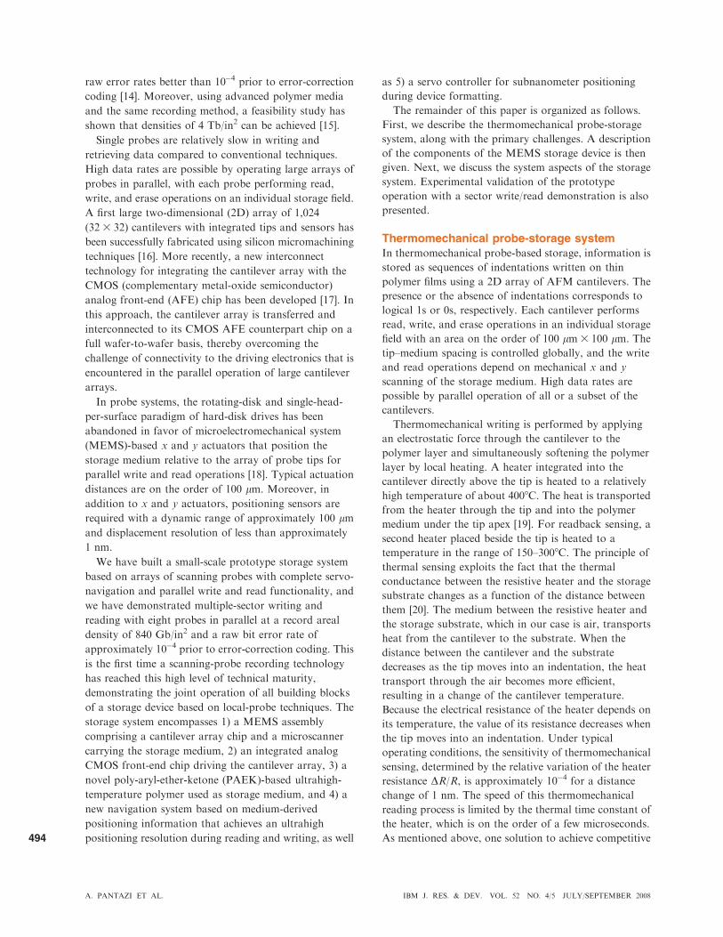
higher-order resonances change with the x/y position,
which further complicates an exact modeling of the
microscanner.
Another important characteristic that describes the
motion of the microscanner is the cross-coupling between
the axes. Figure 3(b) shows the typical cross-coupling on
the y-axis due to x-motion for various values of the
displacement in the y-direction. As shown in Figure 3(b),
the cross-coupling is nonlinear and position dependent.
The experimentally obtained frequency responses for
each direction and the cross-coupling data can be used to
create a microscanner model for controller design and
simulation purposes [23].
Thermal position sensor
Two pairs of thermal position sensors are used to provide
x/y position information of the microscanner to the servo
controller. The sensors consist of thermally isolated,
resistive strip heaters made from moderately doped
silicon [24]. Each sensor is positioned above the edge of
the scan table and heated to a temperature of about
1008C. A fraction of this heat is conducted through the
ambient air into the scan table, which acts as a heat sink.
Displacement of the scan table translates into a change in
the cooling efficiency and hence a change in the
temperature of these heaters. This change in temperature
can be measured as a change in electrical resistance.
Because the sensors are driven with a constant voltage,
these changes in resistance can be detected by measuring
the resulting current. In order to minimize drift effects,
the sensors are operated in pairs using a differential
configuration.
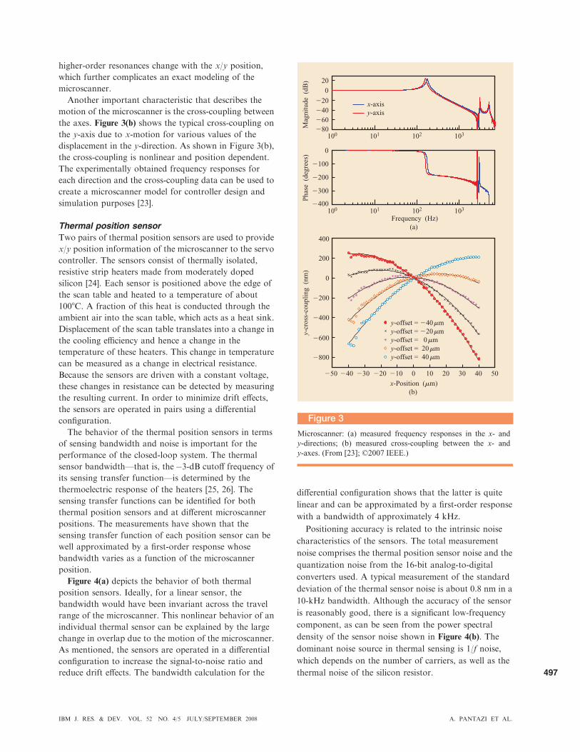
The behavior of the thermal position sensors in terms
of sensing bandwidth and noise is important for the
performance of the closed-loop system. The thermal
sensor bandwidth—that is, the�3-dB cutoff frequency of
its sensing transfer function—is determined by the
thermoelectric response of the heaters [25, 26]. The
sensing transfer functions can be identified for both
thermal position sensors and at different microscanner
positions. The measurements have shown that the
sensing transfer function of each position sensor can be
well approximated by a first-order response whose
bandwidth varies as a function of the microscanner
position.
Figure 4(a) depicts the behavior of both thermal
position sensors. Ideally, for a linear sensor, the
bandwidth would have been invariant across the travel
range of the microscanner. This nonlinear behavior of an
individual thermal sensor can be explained by the large
change in overlap due to the motion of the microscanner.
As mentioned, the sensors are operated in a differential
configuration to increase the signal-to-noise ratio and
reduce drift effects. The bandwidth calculation for the
differential configuration shows that the latter is quite
linear and can be approximated by a first-order response
with a bandwidth of approximately 4 kHz.
Positioning accuracy is related to the intrinsic noise
characteristics of the sensors. The total measurement
noise comprises the thermal position sensor noise and the
quantization noise from the 16-bit analog-to-digital
converters used. A typical measurement of the standard
deviation of the thermal sensor noise is about 0.8 nm in a
10-kHz bandwidth. Although the accuracy of the sensor
is reasonably good, there is a significant low-frequency
component, as can be seen from the power spectral
density of the sensor noise shown in Figure 4(b). The
dominant noise source in thermal sensing is 1/f noise,
which depends on the number of carriers, as well as the
thermal noise of the silicon resistor.
Figure 3
Microscanner: (a) measured frequency responses in the x- and y-directions; (b) measured cross-coupling between the x- and y-axes. (From [23]; ©2007 IEEE.)
100 101 102 103
100 101 102 103
0
Frequency (Hz)(a)
x-axisy-axis
�80�60�40�20
020
�400
�300
�200
�100
�50 �40 �30 �20 �10 0 10 20 30 40 50x-Position ( m)
(b)
y-offset = �40 my-offset = �20 my-offset = 0 my-offset = 20 my-offset = 40 m �800
�600
�400
�200
0
200
400
��
���
�
Mag
nitu
de (
dB)
Phas
e (
degr
ees)
y-cr
oss-
coup
ling
(nm
)
IBM J. RES. & DEV. VOL. 52 NO. 4/5 JULY/SEPTEMBER 2008 A. PANTAZI ET AL.
497

Polymer medium
The polymer medium plays a crucial role in
thermomechanical data storage. The rationale behind the
polymer medium design relates to basic physical
principles underlying the formation of nanoscale indents.
When an indent is written, the medium is in essence
elastically deformed, and the deformation is locked by the
discrete nature of monomer reconfigurations within the
polymer backbone, termed a-transitions. The a-transitionactivity can be enhanced by applying thermal and
mechanical energy during writing, which renders the
polymer easily deformable. At the end of the write event,
the heat and the pressure are turned off within less than
1 ls, causing the activity to slow down by orders of
magnitude, thereby locking the indent in its deformed
state. This kinetic switching provides the memory
function of the polymer medium. However, the indent
representing a bit is a metastable object [5]. The
mechanical stress associated with the deformation
provides a restoring driving force, but the relaxation is
kinetically hindered by the slow a-activity. It is important
to note that the writing of an indent does not involve
irreversible processes such as the breaking of chemical
bonds or the diffusive motion of polymer chains.
The essential criteria for a polymer storage medium are
low-mechanical-stress writing conditions in order to
minimize tip wear, thermal and mechanical robustness in
order to prevent chemical degradation, and repeated
erasability of written indentations. These rather
straightforward requirements contrast with the huge
space spanned by parameters that influence the
thermomechanical properties. Tip temperature,
indentation force, and heating and loading times can be
controlled for a given tip–medium combination. The
shape, radius, and opening angle of the tip, as well as the
chemical composition of the polymeric storage medium,
including cross-linking, are additional parameters
[19, 27, 28]. Despite the complexity, a small number of
design rules have been identified as being crucial for the
polymer media. First, the glass transition temperature,
which sets the temperature scale for the a-transitionactivity of the material, should be in the range 150–1908C,
the lower bound being dictated by bit retention
requirements and the upper bound being dictated by low-
stress writing conditions. Second, a high degree of cross-
linking (chemical bonds between polymer chains) is
needed in order to be able to write and erase the same bit
for thousands of times and to preserve the shape of the bit
during read operation. Cross-linking constrains the
mobility of the polymer chains by providing a firm
interconnection network that effectively suppresses
diffusive motion [29]. The network also acts as an elastic
matrix enhancing the erase functionality by furnishing a
well-defined restoring force. Third, the polymer should be
thermally stable, enabling one to use high-temperature,
low-force writing conditions, which are favorable for
minimizing tip degradation and indent relaxation.
Finally, a parameter known as the yield activation energy,
which describes the energy barrier associated with the
a-transitions, must be greater than approximately 4 eV in
order for thermally activated relaxation to be sufficiently
slow such that the data can be retained for more than
10 years at 858C, as is required for a typical portable
device. It may appear surprising that the last requirement
can be met at all with polymers.
Poly-aryl-ether ketones provide a particularly well-
suited polymer system for our purposes by combining
excellent thermal stability with the ability to tune the
glass transition temperature and cross-link density over a
wide range. The polymer medium used in this study had a
targeted molecular weight of 4,000 and incorporated
diresorcinol in the backbone and ethynyl groups for
Figure 4
Thermal position sensor: (a) measured bandwidth as a function of microscanner position; (b) measured noise power spectral density.
�50 �40 �30 �20 �10 0 10 20 30 40 503.4
3.6
3.8
4.2
4.0
4.4
4.6
4.8
Microscanner position ( m)(a)
Ban
dwid
th (
kHz)
First thermal sensorSecond thermal sensorDifferential sensor
�
100 101 102 103 104 10510�5
10�4
10�3
10�2
10�1
Frequency (Hz)(b)
Pow
er s
pect
ral d
ensi
ty (
nm2 /
Hz)
A. PANTAZI ET AL. IBM J. RES. & DEV. VOL. 52 NO. 4/5 JULY/SEPTEMBER 2008
498

cross-linking functionality. The glass transition
temperature was in the targeted range, and the yield
activation energy was empirically determined to be on the
order of 5 eV. By fine-tuning the cross-link density, more
than 2,500 erase cycles were experimentally demonstrated
at 1 Tb/in2. No loss of signal quality was observed in
these experiments, suggesting that substantially more
cycles are possible, yet not experimentally confirmed
because of technical limitations requiring months of
continuous observation in order to extend this limit by
another order of magnitude. Another critical issue is the
endurance of the written information as a function of
time and repeated reading events with the same tip.
Endurance and wear studies are predominately conducted
using experimental test stands with piezo-scanners and
single cantilever functionality [19, 27, 28]. It was
experimentally demonstrated that one and the same bit
can be repeatedly read at least 2 3 105 times without loss
of signal quality and that the tip is able to sustain 700 m
of travel corresponding to the reading of 531010 symbols
at 1 Tb/in2. Note that also here, the limits are given by the
duration of the experiment and not by the material
limitations. An experiment demonstrating the repetitive
reading of the same track over a period of 3 months is
shown in Figure 5(a). This experiment was performed on
the prototype system that offers the additional flexibility
of being able to locate the same position with nanometer
accuracy. In the first month, we conducted four
experiments with the tip reading approximately 1.5 3 107
symbols. Another two experiments were conducted
during the next 2 months with the tip reading in total
approximately 2.5 3 107 symbols. Note that between
experiments, no reading or writing operations were
performed. As shown in Figure 5(a), aside from an initial
small relaxation of the indentations, the average value of
the measured bit depth is not reduced over time and with
repetitive reads.
Other important characteristics that affect the
performance of the prototype system are medium noise
and indentation depth. Medium noise manifests itself in
the readback signal as variations of the nominal signal
amplitude. It originates from the storage medium
structure that is not perfectly flat but exhibits finite
surface roughness. On the other hand, the indentation
depth affects the signal amplitude level. However, at high
storage densities, variations on the signal amplitude level
occur because of a nonlinear interaction mechanism
between indentations, called partial erasing [30].
Specifically, in thermomechanical writing on polymers,
the creation of a new indentation too close to an existing
one can result in a partial erasing of the existing
indentation. The recording performance can be
characterized using the signal-to-distortion ratio (SDR),
which quantifies the influence of all the distortions on the
readback signal. The SDR depends on the indentation
depth, measured by the average amplitude levels of 0s and
1s, as well as on the variance of the total distortion, that
is, the deviations around the average amplitude levels.
The overall recording performance depends on the
writing parameters such as heater temperature, applied
force, and heating time. In order to investigate how the
recording performance depends on the operating
parameters, random data were recorded with various
parameter sets, and the SDR was calculated from the
captured readback signals. Figure 5(b) shows the
measured SDR in decibels as a function of the write
voltage on the cantilever and the heating time. The
readback signals used to calculate the SDR are shown for
two cases. Specifically, in this experiment, the loading
force was kept constant while the applied voltage, which
predominately affects the heater temperature, was varied
from 4 to 7 V and the heating pulse duration varied from
4 to 10 ls. It can be seen that the recording performance
Figure 5
Polymer medium: (a) repetitive reading of the same track over a period of 3 months at 840 Gb/in2. Each color corresponds to a reading at different time instants. For example, in the first month, we conducted four experiments at different time instances. (b) Measured signal-to-distortion ratio (SDR) for different operating conditions at 840 Gb/in2.
0 0.5 1.0 1.5 2.0 2.5�107
0.5
0.6
0.7
0.8
0.9
1.0
1.1
Number of symbols read(a)
4.05.5
7.0
4.06.08.010.00
2
4
6
8
10
Write (V)Duration ( s) �
Nor
mal
ized
ave
rage
d bi
t dep
thSD
R (
dB)
(b)
1stmonth
2ndmonth
3rdmonth
IBM J. RES. & DEV. VOL. 52 NO. 4/5 JULY/SEPTEMBER 2008 A. PANTAZI ET AL.
499

strongly depends on the amplitude and the duration of
the applied voltage. Below certain values, no indentations
can be obtained; above a certain threshold, the
performance increases when either the amplitude or the
duration of the applied write pulse is increased. For high
storage densities, further increases in the operating
conditions result in increasing the nonlinear partial
erasing effects between adjacent bits. Other parameters,
such as the loading force, have similar effects, as expected.
The SDR measure can be used to characterize the effect
of the operating parameters of the system on the
recording performance.
System aspectsFrom a system point of view, a probe-storage device
comprises a servo controller for navigation and
nanopositioning, a read channel including the data and
servo detectors, and the dataflow encompassing the
modulation and error-correction functionality. The servo
controller uses the positional information obtained from
the thermal sensors and from dedicated fields on the
storage medium to derive the control signals for the
electromagnetic coil actuators of the microscanner [23].
The main challenge for the servo controller is the extreme
precision in navigating the probe tips to the desired
position that is required for ultrahigh-density data
storage. The data read channel is responsible for
retrieving the information from the readback waveform
of the thermomechanical recording channel [30]. Effective
detection schemes are needed to enhance the recording
performance in the presence of signal distortions and
nonlinearities at high storage densities. Finally, the
dataflow includes all functions related to the host
interface, that is, error-correction coding, constrained
coding, data formatting, and interleaving. The flexibility
offered by the large number of probes that operate in
parallel can be exploited at the system level to increase the
error-correction capability, the storage efficiency, and the
reliability of the system. The system components are
described in the following sections.
Position error signal and servo channel
The thermal position sensors can provide high-precision
measurements of the microscanner position but tend to
suffer from low-frequency drift. Therefore, a control
scheme relying on the thermal sensors alone is not
suitable for long-term operation of the device. An
alternative medium-derived position error signal (PES)
can be obtained by reading prewritten servo patterns on
dedicated servo fields. These servo fields are a small
number of storage fields that are reserved exclusively for
servo-control purposes. The approach for PES generation
is based on the concept of vertically displaced bursts,
arranged in such a way as to produce two signals in
quadrature that guarantee a uniquely decodable PES,
that is, each PES value is mapped to a unique cross-track
position [6]. Therefore, the medium-derived PES
accurately captures deviations from the track centerline
for each data track.
Medium-derived PES can be generated using the servo
burst configuration illustrated in Figure 6. The A, B, C,
and D bursts are written in four different servo fields.
Servo bursts labeled A and B are used to create the in-
phase signal (I), and C and D to create the quadrature
signal (Q). The cross-track distance between indentation
centers of the same burst is equal to the track pitch (TP),
whereas the distance between indentation centers in
bursts A and B (or C and D) is TP/2. The distance
between A and C is TP/4. The track centerlines of the
data fields coincide with the centers of servo burst C. For
PES generation, a parallel read operation of the four
servo fields is performed while scanning in the x-direction.
The amplitude of the readback signal depends on the
position of the tip relative to the recorded surface at the
time of reading. The readback signal is strongest when the
tip is positioned exactly over the center of the written
indentation. As the distance of the tip from the
indentation center increases, the readout signal strength
decreases, reaching a minimum level when the tip is away
from the indentation. To generate the PES, four samples
of the readback signal for each written indentation are
used for correlation with a pulse shape representing a
typical indentation and for estimating the indentation
depth. The oversampling of four samples is used to
minimize the impact of timing imperfections on the
system. To reduce the effect of noise on the PES, the
estimated indentation depth values are then filtered. The
average values �A, �B, �C, and �D, corresponding to bursts A,
B, C, and D, are then used to calculate the in-phase signal
as the difference �B � �A and the quadrature signal as the
difference �D� �C. Note that the quadrature signal exhibits
zero crossings at the points where the in-phase signal has
local extrema. The final PES is generated by combining
the two signals (I and Q) and has zero crossings at all
track center locations, and an almost linear range
between �TP/2 and TP/2. The medium-derived PES
provides y-positional information around the track
centerline and, therefore, has a maximum range of TP.
Unlike the thermal position sensor, the medium-derived
PES does not suffer from low-frequency noise.
Servo controller
The main function of the servo controller in the MEMS-
based storage system is to ensure accurate positioning of
the probes over the storage medium so that data tracks
are uniformly written and read back with sufficient
accuracy to guarantee a low error rate. As the areal
density of the system is increased to the terabit-per-
A. PANTAZI ET AL. IBM J. RES. & DEV. VOL. 52 NO. 4/5 JULY/SEPTEMBER 2008
500

square-inch regime and beyond, the performance
requirements for the servo system become very stringent.
In general, the servo system in such a storage device has
two functions. First, it locates the target track to which
information is to be written or read back from, starting
from an arbitrary initial position of the scan table
carrying the storage medium. This is achieved by the
seek-and-settle procedure. Because actuation distances
typically are on the order of 100 lm and the components
have small masses, the positioning delays are much
smaller than in disk drives. Experiments have yielded
remarkably short seek times, on the order of 1 ms for
the worst-case seek operation [23, 31]. The second function
of the servo system is to maintain the position of the
read/write probes on the center of the target track while
scanning along the length of this track. This is achieved
by the track-follow procedure. During the track-follow
procedure, each track is scanned in the horizontal
direction with constant velocity while maintaining the fine
positioning in the cross-track direction in the presence of
disturbances and noise. At the end of each track, a short
seek operation is used to move to the next track [32]. In
addition to the two main servo functions needed in a
normal device operation, the servo information yielding
the medium-derived PES must be written in the servo
fields prior to using the MEMS storage device. Precise
writing of these servo fields is of great importance for
reliable operation of the storage device. Servo controllers
that provide such subnanometer precision have been
designed for this purpose.
In the prototype system, track-follow control along the
scanning direction (x-direction) is based solely on the
thermal position sensor information. In contrast, the
track-follow controller for the y-direction employs both
the global position information from the thermal sensors
and the medium-derived PES. There are separate
controllers for the x- and y-motion of the microscanner,
each one consisting of a linear quadratic Gaussian (LQG)
regulator, a tracking controller, notch filters, and a feed-
forward component. The control architecture depicted in
Figure 7 shows a block diagram of the feedback loop for
one direction of motion. In this figure, P denotes the
dynamics of motion of the microscanner in one direction
and S represents the dynamics of the thermal sensor.
Furthermore, r is the reference signal and y stands for the
motion of the microscanner. The variables di, d, and n
denote the input disturbance, the output disturbance, and
the noise signals, respectively. A set of notch filters, NF, is
incorporated into the feedback loop to minimize the effect
of the higher-order resonances of the microscanner. The
feed-forward component, KFF, is selected to be equal to
the inverse of the dc gain of P to achieve better tracking
performance. The tracking controller has a two-input
one-output structure and can be described by a transfer
function KI from the thermal sensor error signal to the
output and a transfer function KII from the PES to the
Figure 6Position error signal and servo-channel configuration. (TP: track pitch; PES: position error signal.)
Input buffersfor servo levers
Servo channelReference signal:indentation profile
y
TP
PESi
PES
1
0
�11
0
�1
A-field D-field
C-fieldB-field
A
A
Position error signal B − A D − C
CorrelationBit-depthestimation
Bit-depthfiltering
PESq
IBM J. RES. & DEV. VOL. 52 NO. 4/5 JULY/SEPTEMBER 2008 A. PANTAZI ET AL.
501

output. For the x-direction, no medium-derived PES
information is available; therefore, this signal is set to
zero, and control is based exclusively on the thermal
position sensors.
The primary purpose of the feedback controller in the
x-direction is to maintain a constant velocity while
writing and reading information. This requirement can be
translated into the ability of the closed-loop system to
track the reference signal, to mitigate the effect of external
shocks and vibrations, and to reduce the effect of sensor
noise on the position of the microscanner. A detailed
analysis based on closed-loop transfer functions is given
in References [23] and [33]. From the transfer function
analysis, a reference tracking bandwidth of more than
1 kHz and a rejection capability for disturbances of up to
approximately 300 Hz have been shown. From the noise
sensitivity transfer function and the thermal sensor noise
characteristics described in the previous section, the
impact of measurement noise to the system can be
estimated [33]. The standard deviation of the estimated
microscanner perturbation due to measurement noise was
found to be about 0.7 nm [34]. It has been verified that
these nanometer-scale microscanner perturbations while
scanning in the x-direction are the primary source of the
timing jitter in the readback signal [34]. The error rate
performance of the storage device depends on the amount
of timing jitter in the readback signal. Therefore, the
accuracy of the thermal position sensors and the noise
sensitivity characteristics of the closed-loop system are
crucial parameters determining the reliability of the high-
density storage system.
The main purpose of the feedback controller in the
y-direction is to maintain the position of the probes on
the track centerline while writing and reading from a
specific track. Deviations of the probes from the track
centerline result in signal-to-noise ratio (SNR) loss in the
readback signal. The challenges for the y-controller
originate from the disturbance-rejection requirements and
the low-frequency noise characteristics of the thermal
sensor signal. In addition to external shocks and
vibrations, the feedback loop must mitigate the
disturbances that originate from cross-coupling in the
y-position due to the scanning motion in the x-direction.
In a control scheme based solely on thermal sensor
information, drift and low-frequency sensor noise may
cause deviations from the track centerline. To address this
problem, the y-axis feedback loop employs both the
global-position information from the thermal sensors and
the medium-derived position information in a two-
sensor-controller configuration. With the a priori
knowledge of the noise characteristics of both sensors, the
controller can be designed such that the positional
information from the medium-derived PES is primarily
used for control at low frequencies. References [23] and
[35] present a novel control architecture based on the H‘
control framework that uses the best measurement in
different frequency regions. For the small-scale
prototype, an alternate suboptimal two-sensor scheme
was developed and implemented. This scheme is
illustrated in Figure 7, where estimation and regulation
are based only on the thermal sensor signal, as in the case
of the x-direction control. The frequency separation in
this scheme is assigned to the tracking controller, which is
different for each of the sensors. The final positioning
error is a combination of the individual contributions of
each sensor. Using the closed-loop transfer functions, the
standard deviation of the total y-positioning error has
been estimated to be approximately 0.6 nm, which is
expected to be within the tolerable limits.
Data read channel
In this section, we describe the read channel implemented
for each cantilever. The complete read signal path
consists of the read/write physical process and the data
read channel. The read channel consists of an analog
electronics part (also called the analog front end ) and a
digital part, as illustrated in Figure 8. In this figure, a
model of the read signal path is shown, in which the
channel input symbols are denoted by ak and the
continuous readback signal by r(t). By modulating an
underlying write pulse represented by the delta function
d(t), the sequence of channel input symbols is
transformed into a continuous-time write signal, which is
used to store the information in the medium. When the
stored information is read back, the signal obtained is a
distorted version of the corresponding write signal. This
distortion is the result of the combined action of the write
and read processes and is represented by the storage
Figure 7
Control architecture. Here, u is the control current. P indicates a model estimating the response of the microscanner (P). The minus sign near the bottom left arrowhead indicates a subtraction operation for the signal. (LQG: linear quadratic Gaussian.)
Trackingcontroller
LQG regulator
Microscanner/sensors
r
dudi
n
y
KFF
r
�
PES KII
KI NF P
�K
S
P
A. PANTAZI ET AL. IBM J. RES. & DEV. VOL. 52 NO. 4/5 JULY/SEPTEMBER 2008
502

channel. The typical channel in probe storage resembles a
truncated sinc function but is not necessarily symmetrical
around the main lobe. Figure 8 depicts a channel
response that has been extracted by least-squares fitting
of a heavily oversampled, experimentally obtained
readback waveform with a symbol spacing of 20 nm. The
readback signal is corrupted by noise and distortions of
various forms. Two primary noise sources exist:
1) electronics and head noise and 2) medium noise. The
former is usually a combination of an additive white
Gaussian noise process with a 1/f component, and the
latter is modeled as an additive colored Gaussian process.
This choice was validated by an extensive analysis of
experimentally obtained readback waveforms, which
revealed that medium noise exhibits rapid roll-off at high
frequencies and is Gaussian distributed. In the diagram of
Figure 8, n(t) denotes the combined contribution of
electronics and medium noise.
The two significant sources of distortion in the
readback signal are read and write jitter. Write jitter
arises from deviations in the actual positions of the write
pulses with respect to their intended positions. It can be
modeled by a random deviation in the position of the
write pulses and is represented by Dk in Figure 8. Read
jitter can be modeled as random deviations of the
sampling instants from their nominal temporal positions.
There are several possible sources of read/write jitter.
Characterization of the random nanometer-scale
perturbations of the microscanner has shown that these
random perturbations are the predominant source of
read/write jitter [34].
The analog part of the read channel is implemented in
the integrated AFE CMOS chip that includes the
complete circuitry to support parallel operation of the
cantilevers [21, 22]. The design of the on-chip read-
channel circuitry allows reliable detection of the tiny
signal current obtained with the thermal sensing scheme
(DR/R , 10�3 for a typical indentation). This small
sensitivity of the thermal sensing scheme leads to a large
offset current. Therefore, the information-carrying signal
can be viewed as a small signal superimposed on a very
large offset. The bulk of this offset is canceled by means of
an identically biased reference element directly in the
input stage of the AFE chip to minimize power. The
current from the input stage is converted to a differential
voltage signal. A high-pass filter is then used to remove
the remaining bias current and low-frequency noise but
can be bypassed during calibration. Two instrumentation
amplifiers with programmable gain and bandwidth ensure
the flexibility necessary to adapt the transfer function of
the front end to a wide range of operating conditions. An
additional offset-compensation stage between the second
and third amplifier is used to cancel the input offset of the
amplifiers in high-gain configurations. A sample-and-
hold stage is used to synchronously sample all data
channels before the outputs are sequentially multiplexed
to the ADC (analog-to-digital converter).
In the digital domain, the sequence at the output of the
ADC is first synchronized to the symbol rate. This is
accomplished through a timing recovery loop and an
interpolator, which are schematically represented by the
sampling rate converter (SRC) in Figure 8. The timing
loop comprises a second-order PLL (phase-locked loop)
Figure 8
0 20 40 60 80 100 120Sample index
Cha
nnel
impu
lse
resp
onse
(V
)
�0.5
�0.4
�0.3
�0.2
�0.1
0
0.1
0.2
Data read channel. (HPF: high-pass filter; offset comp: offset compensation.) (Data curve from Reference [34]; ©2007 IEEE.)
HPF
offsetcomp
ADC
SRC
Reference
sample&hold
Read channel: analog part
Read channel: digital part
Read signal model
ak
âk
�k
�(t) p(t)
fkrk
a(t)
r(t) rn
n(t)
IBM J. RES. & DEV. VOL. 52 NO. 4/5 JULY/SEPTEMBER 2008 A. PANTAZI ET AL.
503

Figure 9(a) Dataflow architecture. (b) “Write sector” procedure for 512-byte sector. (CRC: cyclic redundancy check; ECC: error-correcting code; RS: Reed–Solomon code; mux: multiplexer; AFE: analog front end; demux: demultiplexer.)
AFE
AFE
Modulationdecoding
DetectionUserdata(sector)
(RS decoder)
Modulationdecoding
Detection
512Initialsectordata
516
CRC-32
22
Parity
129
codeword
32 sub-blocks
20
32 (d,k) coded blocks
20
12 bits
8 bits
32
12
Multiplexed 32 � 12 blocks
12
32Data pattern
32
240+
CRC ECC De-interleaving
Modulationdecoding
Userdata(sector)
(RS encoder)
Modulationdecoding
CRC ECC Interleaving
MuxDemux
Mux Demux
RS
(a)
(b)
A. PANTAZI ET AL. IBM J. RES. & DEV. VOL. 52 NO. 4/5 JULY/SEPTEMBER 2008
504

driven by an error signal derived by the deviations of the
positions of zero-crossings of the derivative of the
readback signal. Finally, the synchronous output of the
interpolator is filtered and passed to a binary adaptive-
threshold detector to produce estimates of the stored
symbols. One of the functions of the digital filter (fk) in
front of the detector is to eliminate rapid dc fluctuations
at the detector input by introducing a null at dc. To
improve the bit error rate, an additional detector is used
in cascade with the threshold detector, which is not
shown in the figure. This detector acts on the output of
the threshold detector and locates and corrects violations
of the d-constraint, that is, the minimum number of 0s
between two 1s imposed by the constrained code. In our
prototype system, we have used a d ¼ 1 code, which
implies that a 0 (no indentation) is always enforced
between two successive 1s (indentations). As these
constraint violations account for the vast majority of
errors, a substantial improvement in the bit error rate is
obtained.
Dataflow
The dataflow includes all functions related to the host
interface, error-correction coding, constrained coding,
data format, and data interleaving. It also provides the
necessary parameters to the servo controller and in
general supervises the complete system functionality. It
receives the user data (sectors) and generates the data
blocks that are stored in each storage field. The data
processing is performed in order to handle the errors
(random or bursts) introduced during the write/read
operations, reallocate and restructure the data for
maximizing the storage efficiency of the device, and adapt
the data stored in each storage field to the channel
characteristics using a proper constrained coding scheme.
As shown in Figure 9(a), during a ‘‘write sector’’
operation, a cyclic redundancy check (CRC) is appended
to the initial data, thus enabling the detection of any
erroneously reconstructed data block in the receiver. For
error correction, a Reed–Solomon (RS) code is used
along with proper interleaving. The number of code-
words and the parity symbols per code-word determine
the total system storage efficiency along with any
additional padding. The device reliability is determined
by the statistics of the channel errors introduced, the RS
code used, and the interleaving scheme applied. The use
of a stronger RS code increases reliability but also
increases the redundancy introduced, so the storage
efficiency decreases. By exploiting the 2D structure of the
data probes, a logical organization in small subdevices
can be used, and a new interleaving technique has been
developed that results in improved reliability for a given
RS code and minimization of the additional padding
required. A new data-allocation method has also been
developed that performs writing of unequal-length data
blocks using parallel operating probes [36]. Figure 9(b)
describes the write sector procedure for a sector of
512 bytes (note that the dataflow supports sector sizes of
both 512 and 1,024 bytes). Specifically, the block
generated by the user data and the appended CRC is split
into a number of data words (determined by the
interleaving depth), and each data word is processed by
an RS encoder. The generated code-words are
interleaved, header and trailer information is appended,
and the data blocks stored in each storage field are
processed by a (d, k) constrained code encoder. The
constrained codes impose restrictions on the number of
consecutive 1s and 0s in the encoded data sequence. The
code parameters d and k are nonnegative integers, with
k . d, where d indicates the minimum number of 0s
between two 1s, and k indicates the maximum number of
zeros between two 1s. For our recording device, the most
important constraint is the d-constraint because it
determines the distance of consecutive indentations. As
mentioned above, we have selected d¼ 1.
Because the write operation of the device is a type of
demultiplexing into the various channels, multiplexing is
also performed on the encoded data blocks in order to
generate the final write pattern. When the data probes are
directly above the proper position in each storage field,
this write pattern is used by the AFE circuitry to perform
the write operation. The reverse procedure is performed
during a ‘‘read sector’’ operation.
Storage system demonstration
A small-scale storage system prototype (shown in
Figure 10) comprising all of the critical components
presented in the previous sections has been built and its
Figure 10
Storage system prototype.
CMOSAFEchip
MEMSassembly
IBM J. RES. & DEV. VOL. 52 NO. 4/5 JULY/SEPTEMBER 2008 A. PANTAZI ET AL.
505

functionality experimentally verified. A personal
computer was connected through the host interface with
the electronics board that hosts the MEMS assembly and
the AFE chip. The AFE chip was interconnected by wire
bonding to the cantilever array chip. The interface
between the AFE electronics and the host PC was
implemented in an onboard digital signal processor
(DSP) and field-programmable gate array (FPGA)
configuration and supports standard read/write sector
commands. The system components of the small-scale
prototype were implemented on the onboard DSP/FPGA
configuration.
Three ASCII files were transformed in three user
sectors of 1,024 bytes each. The sectors were processed by
all stages of the dataflow presented in the previous
section. The resulting symbol sequences were stored in
four different data fields occupying three different data
tracks in each field. The track size spanned 90 lm in the
x-direction, and the distance between adjacent tracks was
32 nm in the y-direction. Each track contained 5,300
symbols, and the distance between adjacent symbols was
16 nm. The resulting effective areal storage density was
840 Gb/in2. During reading of the stored information, the
two-sensor controller presented in the previous section
was used to ensure convergence to the track centerline,
accurate positioning during the track-follow procedure,
and reliable stepping to the subsequent tracks. The
readback signals from the levers were processed by the
read channel described in the previous section, and the
symbols of each track were detected with an error rate of
approximately 10�4 prior to error-correction coding.
After the reverse operation of the dataflow, the complete
sector information was recovered from the ECC module.
Figure 11 shows the readback signal from four cantilevers
and three different tracks. Each row represents a different
cantilever waveform with data from three data tracks. A
close-up of a portion of the readback signal shown in the
figure demonstrates the recording quality. In Figure 11,
the error-free information of the readback sectors is also
shown (upper left). This is the first time that an areal
Figure 11Sector write and read demonstration at 840 Gb/in2.
1 2 3 4Number of readback samples
Rea
dbac
k si
gnal
(V
)
�0.20
0.2
�0.20
0.2
�0.20
0.2
�0.20
0.2
�104
�0.2
0
0.2
A. PANTAZI ET AL. IBM J. RES. & DEV. VOL. 52 NO. 4/5 JULY/SEPTEMBER 2008
506
storage density demonstration of 840 Gb/in2 has been
performed with all the building blocks of a storage device.
ConclusionUltrahigh densities beyond 1 Tb/in2 can be achieved by
probe-based storage technologies. A small-scale
prototype demonstrating all the basic functions of a
storage device based on scanning probes has been
presented in this paper. Starting from the basic principle
of operation all the way to the higher-level system
functionality, the building blocks have been described
and experimentally characterized. The complete
prototype system functionality was verified with
experimental results of multiple sectors recorded using
multiple levers at 840 Gb/in2 and read back without
errors. This is the first scanning probe-storage technology
for which ultrahigh areal density recording and reliable
retrieval have been demonstrated using a fully functional
storage device prototype.
Although tremendous progress has been made from the
initial concept to the building of a fully functional
prototype storage system, more technical challenges need
to be addressed prior to commercializing such a new
technology. These challenges include optimal tradeoff
between number of tips, data rate, and power
consumption, tracking of more than 1,000 probes at
subnanometer resolution, process improvements for
controlled cantilever-array homogeneity, further
characterization and optimization of tip–medium
interaction, and finally, thorough assessment of system-
level reliability.
AcknowledgmentsWe thank our colleagues G. Binnig and P. Vettiger for
their pioneering work and initiation of the ‘‘Millipede’’
project. We also thank J. Frommer, B. Miller, J. Mamin,
J. Gordon, and T. Magbitang of the IBM Almaden
Research Center for their invaluable contributions to the
polymer media work. We thank T. Albrecht and J.
Windeln for contributions to the progress of the project.
Finally, we would like to thank our colleagues P. Seidler
and W. Bux for their continued support of this project.
**Trademark, service mark, or registered trademark of the Blu-rayDisc Association in the United States, other countries, or both.
References1. H. J. Mamin, L. S. Fan, S. Hoen, and D. Rugar, ‘‘Tip-Based
Data Storage Using Micromechanical Cantilevers,’’ Sensors &Actuators A 48, No. 3, 215–219 (1995).
2. C. F. Quate, ‘‘Method and Means of Data Storage UsingTunnel Current Data Readout,’’ U.S. Patent No. 4,575,822,1986.
3. H. J. Mamin, B. D. Terris, L. S. Fan, S. Hoen, R. C. Barrett,and D. Rugar, ‘‘High-Density Data Storage Using ProximalProbe Techniques,’’ IBM J. Res. & Dev. 39, No. 6, 681–700(1995).
4. H. J. Mamin, R. P. Ried, B. D. Terris, and D. Rugar, ‘‘High-Density Data Storage Based on the Atomic ForceMicroscope,’’ Proc. IEEE 87, No. 6, 1012–1013 (1999).
5. P. Vettiger, G. Cross, M. Despont, U. Drechsler, U. Durig,B. Gotsmann, W. Haberle, et al., ‘‘The ‘Millipede’—Nanotechnology Entering Data Storage,’’ IEEE Trans.Nanotechnol. 1, No. 1, 39–55 (2002).
6. E. Eleftheriou, T. Antonakopoulos, G. K. Binnig,G. Cherubini, M. Despont, A. Dholakia, U. Durig, et al.,‘‘Millipede—A MEMS Based Scanning-Probe Data StorageSystem,’’ IEEE Trans. Magn. 39, No. 2, 938–945 (2003).
7. G. Binnig, H. Rohrer, Ch. Gerber, and E. Weibel, ‘‘737Reconstruction on Si(111) Resolved in Real Space,’’ Phys.Rev. Lett. 50, No. 2, 120–123 (1983).
8. G. Binnig, C. F. Quate, and Ch. Gerber, ‘‘Atomic ForceMicroscope,’’ Phys. Rev. Lett. 56, No. 9, 930–933 (1986).
9. S. Gidon, O. Lemonnier, B. Rolland, O. Bichet, C. Dressler,and Y. Samson, ‘‘Electrical Probe Storage Using JouleHeating in Phase Change Media,’’ Appl. Phys. Lett. 85,No. 26, 6392–6394 (2004).
10. H. F. Hamann, M. O’Boyle, Y. C. Martin, M. Rooks, andH. K. Wickramasinghe, ‘‘Ultra-High-Density Phase-ChangeStorage and Memory,’’ Nat. Mater. 5, 383–387 (2006).
11. L. R. Carley, J. A. Bain, G. K. Fedder, D. W. Greve,D. F. Guillou, M. S. C. Lu, T. Mukherjee, S. Santhanam,L. Abelmann, and S. Min, ‘‘Single Chip Computers withMicroelectromechanical Systems-based Magnetic Memory,’’J. Appl. Phys. 87, No. 9, 6680–6685 (2000).
12. H. Park, J. Jung, D.-K. Min, S. Kim, S. Hong, and H. Shin,‘‘Scanning Resistive Probe Microscopy: Imaging FerroelectricDomains,’’ Appl. Phys. Lett. 84, No. 10, 1734–1736 (2004).
13. H. J. Mamin and D. Rugar, ‘‘Thermomechanical Writing withan Atomic Force Microscope Tip,’’ Appl. Phys. Lett. 61,No. 8, 1003–1005 (1992).
14. H. Pozidis, W. Haberle, D. W. Wiesmann, U. Drechsler,M. Despont, T. Albrecht, and E. Eleftheriou, ‘‘Demonstrationof Thermomechanical Recording at 641 Gbit/in2,’’ IEEETrans. Magn. 40, No. 4, 2531–2536 (2004).
15. D. Wiesmann, U. Durig, B. Gotsmann, A. Knoll, H. Pozidis,F. Porro, and R. Vecchione, ‘‘Ultra-High Storage Densitieswith Thermo-Mechanical Probes and Polymer Media,’’Proceedings of the Innovative Mass Storage TechnologiesWorkshop, Enschede, The Netherlands, 2007, pp. 19–20; seehttp://imst2007.ewi.utwente.nl/imst_program.pdf.
16. M. Despont, J. Brugger, U. Drechsler, U. Durig, W. Haberle,M. Lutwyche, H. Rothuizen, et al., ‘‘VLSI-NEMS Chip forAFM Data Storage,’’ Sensors & Actuators A 80, 100–107(2000).
17. M. Despont, U. Drechsler, R. Yu, H. B. Pogge, andP. Vettiger, ‘‘Wafer-Scale Microdevice Transfer/Interconnect:Its Application in an AFM-Based Data-Storage System,’’J. Microelectromech. Syst. 13, No. 6, 895–901 (2004).
18. M. A. Lantz, H. E. Rothuizen, U. Drechsler, W. Haberle, andM. Despont, ‘‘A Vibration Resistant Nanopositioner forMobile Parallel-Probe Storage Applications.’’J. Microelectromech. Syst. 16, No. 1, 130–139 (2007).
19. B. Gotsmann and U. Durig, ‘‘Nano-Thermomechanics:Fundamentals and Application in Data Storage Devices,’’Applied Scanning Probe Methods IV: Industrial Applications,B. Bhushan and H. Fuchs, Eds., Springer, Berlin, Heidelberg,2006, pp. 215–250.
20. U. Durig, ‘‘Fundamentals of Micromechanical ThermoelectricSensors,’’ J. Appl. Phys. 98, No. 4, 044906-1–44906-14 (2005).
21. C. Hagleitner, T. Bonaccio, A. Pantazi, A. Sebastian, andE. Eleftheriou, ‘‘An Analog Frontend Chip for a MEMS-Based Parallel Scanning-Probe Data-storage System,’’Proceedings 2006 Symposium on VLSI Circuits Digest ofTechnical Papers, Honolulu, HI, 2006, pp. 57–58.
22. C. Hagleitner, T. Bonaccio, H. Rothuizen, J. Lienemann,D. Wiesmann, G. Cherubini, J. G. Korvink, andE. Eleftheriou, ‘‘Modeling, Design, and Verification for theAnalog Front-End of a MEMS-Based Parallel Scanning-
IBM J. RES. & DEV. VOL. 52 NO. 4/5 JULY/SEPTEMBER 2008 A. PANTAZI ET AL.
507

Probe Storage Device,’’ IEEE J. Solid-State Circuits 42, No. 8,1779–1789 (2007).
23. A. Pantazi, A. Sebastian, G. Cherubini, M. Lantz, H. Pozidis,H. Rothuizen, and E. Eleftheriou, ‘‘Control of MEMS-BasedScanning-Probe Data Storage Devices,’’ IEEE Trans. ControlSyst. Technol. 15, No. 5, 824–841 (2007).
24. M. A. Lantz, G. K. Binnig, M. Despont, and U. Drechsler,‘‘A Micromechanical Thermal Displacement Sensor withNanometer Resolution,’’ Nanotechnology 16, 1089–1094(2005).
25. D. Wiesmann and A. Sebastian, ‘‘Dynamics of Silicon Micro-heaters: Modelling and Experimental Identification,’’Proceedings of the 19th IEEE International Conference onMicro Electro Mechanical Systems, Istanbul, Turkey, 2006,pp. 182–185.
26. A. Sebastian, D. Wiesmann, C. Hagleitner, and E. Eleftheriou,‘‘Performance Characteristics of a Thermo-electricTopography Sensor,’’ IBM Research Report RZ-3696, 99706,September 25, 2007.
27. B. Gotsmann and U. Durig, ‘‘Thermally Activated NanowearModes of a Polymer Surface Induced by a Heated Tip,’’Langmuir 20, No. 4, 1495–1500 (2004).
28. A. Knoll, P. Bachtold, J. Bonan, G. Cherubini, M. Despont,U. Drechsler, U. Durig, et al., ‘‘Integrating Nanotechnologyinto a Working Storage Device,’’ Microelectronic Eng. 83,1692–1697 (2006).
29. B. Gotsmann, U. Durig, S. Sills, J. Frommer, andC. J. Hawker, ‘‘Controlling Nanowear in a Polymer byConfining Segmental Relaxation,’’ Nano Lett. 6, No. 2,296–300 (2006).
30. H. Pozidis, P. Bachtold, G. Cherubini, E. Eleftheriou,C. Hagleitner, A. Pantazi, and A. Sebastian, ‘‘SignalProcessing for Probe Storage,’’ Proceedings of the IEEEInternational Conference on Acoustics, Speech, and SignalProcessing, Vol. 5, Philadelphia, PA, 2005, pp. 1520–1649.
31. A. Sebastian, A. Pantazi, G. Cherubini, M. Lantz,H. Rothuizen, H. Pozidis, and E. Eleftheriou, ‘‘TowardsFaster Data Access: Seek Operations in MEMS-Based StorageDevices,’’ Proceedings of the IEEE International Conference onControl Applications, Munich, Germany, 2006, pp. 283–288.
32. A. Pantazi, M. Lantz, G. Cherubini, H. Pozidis, andE. Eleftheriou, ‘‘Servomechanism for a MEMS-BasedScanning-Probe Data Storage Device,’’ Nanotechnology 15,S612–S621 (2004).
33. A. Sebastian, A. Pantazi, G. Cherubini, E. Eleftheriou,M. Lantz, and H. Pozidis, ‘‘Nanopositioning for ProbeStorage,’’ Proceedings of the American Control Conference,Vol. 6, Portland, OR, June 8–10, 2005, pp. 4181–4186.
34. A. Sebastian, A. Pantazi, and H. Pozidis, ‘‘Jitter Investigationand Performance Evaluation of a Small-Scale Probe StorageDevice Prototype,’’ Proceedings of the 50th Annual IEEEGlobal Telecommunications Conference, Washington, DC,November 2007, pp. 288–293.
35. A. Pantazi, A. Sebastian, H. Pozidis, and E. Eleftheriou, ‘‘TwoSensor Based H‘ Control for Probe Storage,’’ Proceedings ofthe 44th IEEE Conference on Decision and Control, Seville,Spain, 2005, pp. 1174–1179.
36. M. Varsamou and T. Antonakopoulos, ‘‘A New DataAllocation Method for Parallel Probe-Based Storage Devices,’’IEEE Trans. Magn. 44, No. 4, 547–554 (2008).
Received September 21, 2007; accepted for publication
Angeliki Pantazi IBM Research Division, Zurich ResearchLaboratory, Saumerstrasse 4, 8803 Ruschlikon, Switzerland([email protected]). Dr. Pantazi received a diploma and Ph.D.degrees in electrical engineering and computer technology from theUniversity of Patras, Greece, in 1996 and 2005, respectively. She isa Research Staff Member at the IBM Zurich Research Laboratory,in Ruschlikon. Her research is focused on probe-basedtechnologies with emphasis on nanopositioning and system-leveldesign for probe-based data-storage devices.
Abu Sebastian IBM Research Division, Zurich ResearchLaboratory, Saumerstrasse 4, 8803 Ruschlikon, Switzerland([email protected]). Dr. Sebastian received a B.E.(Hons.)degree in electrical and electronics engineering from Birla Instituteof Technology and Science, Pilani, India, in 1998, and M.S. andPh.D. degrees in electrical engineering from Iowa State Universityin 1999 and 2004, respectively. He is currently a Research StaffMember at the IBM Zurich Research Laboratory. His research isprimarily focused on the application of control theory to nanoscaledevices. He has worked extensively on the analysis of atomic forcemicroscope dynamics and the development of novel modes ofoperation based on a systems perspective. Currently, he is workingon probe-based data storage, focusing on nanopositioning andsystem-level integration of the various components of the storagedevice.
Theodore A. Antonakopoulos Department of Electricaland Computers Engineering, University of Patras, 26500 Rio-Patras,Greece ([email protected]). Dr. Antonakopoulos received adiploma degree in electrical engineering and a Ph.D. degree fromthe Department of Electrical Engineering at the University ofPatras in 1985 and 1989, respectively. In September 1985, he joinedthe Laboratory of Electrotechnics, University of Patras,participating in various R&D projects for the Greek Governmentand the European Union, initially as a Research Staff Member andsubsequently as the Senior Researcher of the CommunicationsGroup. Since 1991, he has been a faculty member of theDepartment of Electrical and Computer Engineering, University ofPatras, where he is currently a Professor and the Director of theLaboratory of Electrotechnics. From 2001 to 2002, he spent hissabbatical at the IBM Zurich Research Laboratory. His researchinterests are in the areas of data communications with emphasis onperformance analysis, efficient hardware implementation, andrapid prototyping. He has more than 110 publications in theseareas and is actively participating in several R&D projects ofEuropean industries. Dr. Antonakopoulos is a senior member ofthe IEEE and a member of the Technical Chamber of Greece.
Peter Bachtold IBM Research Division, Zurich ResearchLaboratory, Saumerstrasse 4, 8803 Ruschlikon, Switzerland([email protected]). Mr. Bachtold received a diploma degree asan Electronics and Telecommunications Technician in 1970. Hejoined the IBM Zurich Research Laboratory in 1977. Presently, hiswork as Senior Engineer concentrates on electronic circuit designfor probe-based technologies and nanopositioning.
Anthony R. (Tony) Bonaccio IBM Systems and TechnologyGroup, 1000 River Road, Essex Junction, Vermont 05452([email protected]). Mr. Bonaccio is a Distinguished Engineer at theIBM microelectronics facility in Essex Junction, Vermont. Sincejoining the analog and mixed-signal design group at IBM in 1979,he has been responsible for the design and development of a widevariety of analog integrated circuit products. His main focus hasbeen on integrated circuits for hard disk drives, including custominterface driver chips, phase-locked loop chips, and low-noise
A. PANTAZI ET AL. IBM J. RES. & DEV. VOL. 52 NO. 4/5 JULY/SEPTEMBER 2008
508
October 22, 2007; Internet publication July 23, 2008

preamplifiers for magnetoresistive heads. From 1993 to 2001, hewas a technical team leader for the development of CMOS andBiCMOS partial-response, maximum likelihood (PRML) datachannel chips for use in IBM mobile and consumer hard diskdrives. His current assignments include high-speed serial interfaceand data converter cores for IBM microprocessors and ASICs, aswell as the Millipede analog front-end and lever modeling effort.Mr. Bonaccio holds a B.S. in electrical engineering from theUniversity of Rochester, New York, and an M.S. in electricalengineering from the University of Vermont. He holds 35 U.S.patents in the area of analog integrated circuit design and has 17pending. He is a Senior Member of the IEEE and an AdjunctProfessor of Electrical and Computer Engineering at the Universityof Vermont, where he has offered graduate-level courses in MOSand bipolar analog circuit design since 1988.
Jose Bonan IBM Research Division, Zurich ResearchLaboratory, Saumerstrasse 4, 8803 Ruschlikon, Switzerland([email protected]). Mr. Bonan received M.S. degrees inmaterial science from Orsay University (Paris, France) and inelectrical engineering from Pierre et Marie Curie University (Paris,France) in 1999 and 2003, respectively. In 1999, he was invited toLawrence Berkeley National Laboratory as a visiting scholar forone year. He currently is a predoctoral student at the IBM ZurichResearch Laboratory, working toward the Ph.D. degree inelectronic engineering at the Pierre et Marie Curie University,Paris, France. His main research interests are in analog and mixed-signal integrated circuit design and analog design automation.
Giovanni Cherubini IBM Research Division, Zurich ResearchLaboratory, Saumerstrasse 4, 8803 Ruschlikon, Switzerland([email protected]). Dr. Cherubini received a Laurea degree inelectrical engineering (summa cum laude) from the University ofPadova, Italy, and M.S. and Ph.D. degrees in electrical engineeringfrom the University of California, San Diego. He joined theresearch staff of IBM in 1987. His research interests include high-speed data transmission and data storage systems. He was coeditorof the 100BASE-T2 Standard for Fast Ethernet transmission overvoice-grade cables. More recently, he contributed to the realizationof the first fully functional atomic force microscope-based data-storage prototype system. Dr. Cherubini was a co-recipient of the2003 IEEE Communications Society Leonard G. Abraham PrizePaper Award. He is Fellow of the IEEE and DistinguishedLecturer of the IEEE Communications Society.
Michel Despont IBM Research Division, Zurich ResearchLaboratory, Saumerstrasse 4, 8803 Ruschlikon, Switzerland([email protected]). Dr. Despont received a degree inmicrotechnology from the Swiss Federal Institute of Technology ofLausanne in 1993 and a Ph.D. degree in physics from the Instituteof Microtechnology, University of Neuchatel, Switzerland, in 1996,with a dissertation on the microfabrication of electron microlensesfor a miniaturized electron microscope. After a postdoctoralfellowship at the IBM Zurich Research Laboratory in 1996, wherehe worked on the development of various cantilever-based sensorsand pioneered the process development of an ultrathick, high-aspect-ratio UV resist called SU-8, he spent one year as a visitingscientist at the Seiko Instrument Research Laboratory in Japan.Since returning to the IBM Zurich Research Laboratory, his workhas focused on the development of micromechanical andnanomechanical devices as well as on 3D microdevice integrationfor system-on-a-chip (SoC) applications.
Richard A. DiPietro IBM Almaden Research Center,650 Harry Road, San Jose, CA 95120 ([email protected]).
Dr. DiPietro earned a B.S. degree at the State University ofNew York at Binghamton in 1976, an M.S. degree in organicchemistry at the University of California, San Diego in 1980, and aPh.D. degree in synthetic medicinal chemistry at the University ofMichigan in Ann Arbor in 1984. Upon completion of apostdoctoral fellowship at Syntex Research, he moved toE. R. Squibb & Sons in New Brunswick, New Jersey, in 1985. Hejoined the Polymer Science and Technology department at the IBMAlmaden Research Center in 1988 as a member of the SyntheticDevelopment Laboratory, where he is currently a Senior Scientist.His interests are the syntheses of monomers, polymers, andassorted organic materials of interest to the electronics industry.
Ute Drechsler IBM Research Division, Zurich ResearchLaboratory, Saumerstrasse 4, 8803 Ruschlikon, Switzerland([email protected]). Ms. Drechsler is a Processing Engineer inthe Science and Technology department of the IBM ZurichResearch Laboratory. She originally joined the IBM Plant inSindelfingen, Germany, in 1983, while also receiving training inchemical engineering. After this, she worked in the fabrication linefor multilayer ceramic packaging, where she was promoted tosection head in 1993. In 1996, she joined the Micro/Nanomechanicsgroup at the Zurich Research Laboratory, working on siliconmicromachining and processing techniques for probe-basedstorage array chips and processing-related work for otherdepartment projects. She is currently responsible for theorganization and operation of the department cleanroom.
Urs Durig IBM Research Division, Zurich ResearchLaboratory, Saumerstrasse 4, 8803 Ruschlikon, Switzerland([email protected]).Dr. Durig received a degree in experimentalphysics and a Ph.D. degree, both from the Swiss Federal Instituteof Technology, Zurich, Switzerland, in 1979 and 1984, respectively.He was a postdoctoral fellow at the IBM Zurich ResearchLaboratory, working on near-field optical microscopy in DieterPohl’s group. In 1986, he became a Research Staff Member andworked in the field of scanning tunneling and force microscopy,investigating metallic adhesion, growth morphology of magneticthin films, and surface melting. In 1997, he joined the ProbeStorage Group at IBM, working on the polymer mediadevelopment.
Bernd Gotsmann IBM Research Division, Zurich ResearchLaboratory, Saumerstrasse 4, 8803 Ruschlikon, Switzerland([email protected]). Dr. Gotsmann studied physics at theUniversity of Munster, Germany, and the University of York,United Kingdom. In 2000, he received a Ph.D. degree in physics forhis work on force detection using dynamic force microscopy. From2001 to 2006, he was a postdoctoral fellow and a visiting scientist inthe Micromechanics/Nanomechanics group of the IBM ZurichResearch Laboratory, working on polymer media design andendurance issues in thermomechanical data storage. Since 2006, hehas been a Research Staff Member at IBM. His current researchactivities are in the fields of nano-tribology, nanoscale heattransfer, and polymer design for thermomechanical applications.
Walter Haberle IBM Research Division, Zurich ResearchLaboratory, Saumerstrasse 4, 8803 Ruschlikon, Switzerland([email protected]). Mr. Haberle is a development engineer inthe Science and Technology department of the IBM ZurichResearch Laboratory. In 1974, he joined the IBM SemiconductorPlant in Sindelfingen, Germany, for his education as physicstechnician and was later promoted to group leader in the QualityControl department of the semiconductor line. In 1987, he joinedthe IBM Physics Group of Professor G. K. Binnig at the University
IBM J. RES. & DEV. VOL. 52 NO. 4/5 JULY/SEPTEMBER 2008 A. PANTAZI ET AL.
509

of Munich, Germany, where he contributed to the development ofatomic force microscopes (AFMs) for applications in a liquidenvironment for investigating living cells. In 1995, he transferred tothe IBM Zurich Research Laboratory, where he was responsiblefor prototyping a new low-cost AFM instrument. Since 1997, hehas been involved in various aspects of the probe-based data-storage project. In 2003, he spent a sabbatical year at the WayneState University in Detroit, Michigan, where he investigated heat-transfer rates in biological samples using thermomechanical levertechnologies. Since 2006, the focus of his research has been on thetape path of tape drive systems.
Christoph Hagleitner IBM Research Division, ZurichResearch Laboratory, Saumerstrasse 4, 8803 Ruschlikon,Switzerland ([email protected]). Dr. Hagleitner obtained adiploma degree and a Ph.D. degree in electrical engineering fromthe Swiss Federal Institute of Technology (ETH), Zurich, in 1997and 2002, respectively. After receiving his Ph.D. degree in 2002with a thesis on a CMOS single-chip gas detection system, heheaded the circuit design group of the Physical ElectronicsLaboratory at the ETH Zurich. In 2003, he joined the IBM ZurichResearch Laboratory in Ruschlikon, Switzerland, where he workson the analog front-end design and system aspects of a novelprobe-storage device.
James L. Hedrick IBM Almaden Research Center,650HarryRoad,SanJose,California 95120([email protected]).Dr. Hedrick received B.S. and Ph.D. degrees from the VirginiaTech in 1981 and 1985, respectively, under the mentorship of Dr.James E. McGrath. He is currently a Research Staff Member at theIBM Almaden Research Center, and he is an investigator in theNSF Center for Polymeric Assemblies and MacromolecularInterfaces. He was the recipient of the 2003 American ChemicalSociety (ACS) Carl S. Marvel Creative Polymer Chemistry Awardand the 2006 ACS Industrial Sponsors Award. His research hasfocused on new synthetic methodologies for microelectronics,nanotechnology, and biocompatible materials using organiccatalysis.
Daniel Jubin IBM Research Division, Zurich ResearchLaboratory, Saumerstrasse 4, 8803 Ruschlikon, Switzerland([email protected]). In 1993, Mr. Jubin received an engineeringdegree in Optronics from L’Ecole Nationale Superieur des SciencesAppliquees et de Technologie in Lannion, France. Until 1997, heworked for a spinoff of the Swiss Federal Institute of Technologyof Zurich, developing an all-solid-state laser for ultrashort pulsegeneration. He then joined JDS-Uniphase, where he participated indeveloping high-power pump laser diodes for erbium-doped fiberamplifiers. In 2001, he joined the silicon-oxynitride waveguideeffort in the IBM Zurich Research Laboratory, where he was incharge of characterizing integrated optical compounds. He movedto the Microfabrication and Nanofabrication group in 2003 and,since then, has been responsible for the characterization of MEMSchips.
Armin Knoll IBM Research Division, Zurich ResearchLaboratory, Saumerstrasse 4, 8803 Ruschlikon, Switzerland([email protected]). Dr. Knoll received an M.S. degree inexperimental physics from the University of Wurzburg, Germany(1998), and a Ph.D. degree in physical chemistry from theUniversity of Bayreuth, Germany, in 2004. During his education,he specialized in scanning probe methods in various environments.In a postdoctoral fellowship with the University of Basel for
15 months (2003/2004), he worked on functional MEMS structuresproduced by two photon polymerization lithography. After avisiting scientist position from 2005 to 2006, he became ResearchStaff Member at the Zurich Research Laboratory in April 2006. Asa member of the Advanced Media Concepts group of the probe-storage project, he is currently working on optimizing polymericmedia for storage applications.
Mark A. Lantz IBM Research Division, Zurich ResearchLaboratory, Saumerstrasse 4, 8803 Ruschlikon, Switzerland([email protected]). Dr. Lantz received B.Sc. and M.Sc.degrees in electrical engineering from the University of Alberta,Canada, in 1991 and 1993, and a Ph.D. degree from the Universityof Cambridge, United Kingdom, in 1997 for work in the field ofscanning probe microscopy. He then spent two years as apostdoctoral researcher at the Joint Research Center for AtomTechnology in Japan, investigating the application of scanningprobes in biophysics, followed by two years of research in the areaof low-temperature scanning force microscopy at the PhysicsInstitute in University of Basel, Switzerland. In 2001, he joined theMicromechanics/Nanomechanics group of the IBM ZurichResearch Laboratory as a Research Staff Member. His currentresearch activities are focused on micromechanical andnanomechanical devices and systems for scanning-probe-baseddata storage, tribology, and magnetic tape drive technology.
John Pentarakis Department of Electrical and ComputerEngineering, University of Patras, 26500 Rio-Patras, Greece([email protected]). Mr. Pentarakis received his engineeringdiploma from the department of electrical and computerengineering at the University of Patras, Greece, in 2004. InSeptember 2004, he joined the Laboratory of Electrotechnics,University of Patras, as a research staff member, participating invarious R&D projects for the Greek government and the industrialsector in the fields of data communications and embedded systems.Currently, he is a post-graduate student at the University of Patras,and his research interests are in the areas of digital communicationswith emphasis on signal detection and coding.
Haralampos Pozidis IBM Research Division, ZurichResearch Laboratory, Saumerstrasse 4, 8803 Ruschlikon,Switzerland ([email protected]). Dr. Pozidis received a diplomadegree in computer engineering and informatics from theUniversity of Patras, Greece, in 1994, and the M.Sc. and Ph.D.degrees in electrical engineering from Drexel University,Philadelphia, Pennsylvania, in 1997 and 1998, respectively. From1998 until 2001, he was with Philips Research (Eindhoven, TheNetherlands), where he worked on read channel design for opticalstorage devices, in particular DVD and Blu-ray** disc formats,with focus on channel modeling, equalization, and bit detection.Since 2001, he has been with the IBM Zurich Research Laboratory,working on basic recording technology, signal processing, andoverall system design for MEMS-based scanning-probe data-storage devices.
Russell C. Pratt IBM Research Division, IBM AlmadenResearch Center, 650 Harry Road, San Jose, California 95120([email protected]). Dr. Pratt received his B.Sc. degree inchemistry from the University of British Columbia, Canada, in1998 and his Ph.D. degree in chemistry from Stanford University,California, in 2004. He then spent one year as a joint Stanford–IBM postdoctoral researcher before becoming a supplemental IBMemployee in the Advanced Organic Materials group in 2005.
A. PANTAZI ET AL. IBM J. RES. & DEV. VOL. 52 NO. 4/5 JULY/SEPTEMBER 2008
510

Hugo Rothuizen IBM Research Division, Zurich ResearchLaboratory, Saumerstrasse 4, 8803 Ruschlikon, Switzerland([email protected]). Dr. Rothuizen studied physics at the SwissFederal Institute of Technology, Lausanne, completing his Ph.D.degree in 1994 with a dissertation on selective-area epitaxial growthof III–V materials. Since becoming a Research Staff Member at theIBM Zurich Research Laboratory in 1996, he has worked on thepatterning of nanometer-scale structures and on the design ofmicromechanical sensors and actuators. He is currently involved inthe modeling of MEMS devices and in the development ofpackaging solutions.
Richard Stutz IBM Research Division, Zurich ResearchLaboratory, Saumerstrasse 4, 8803 Ruschlikon, Switzerland([email protected]). Mr. Stutz is a senior technical specialist inthe Micromechanics/Nanomechanics group of the IBM ZurichResearch Laboratory, which he joined in 1998. His currenttechnical responsibilities and interests include electroplating,plasma sputter deposition, MEMS fabrication, surfacemodification by stamping techniques, and focused ion beammachining for micromechanical devices. Prior to joining IBM, hewas responsible for the fabrication technological aspect ofholography, electroplating, injection molding, stamping, integratedand micro-optical systems as a member of the technical staff of thePaul Scherrer Institute, and the Centre Suisse d’Electronique et deMicrotechnique in Zurich, Switzerland.
Maria Varsamou IBM Research Division, Zurich ResearchLaboratory, Saumerstrasse 4, 8803 Ruschlikon, Switzerland([email protected]). Ms. Varsamou received a diploma degreein electrical and computer engineering from the University ofPatras, Greece, in 2000. After this, she became a graduate studentat the same department in the Laboratory of Electrotechnics. She iscurrently with the IBM Zurich Research Laboratory, inRuschlikon, Switzerland, working on probe-based data storage,with emphasis on error control coding.
Dorothea Wiesmann IBM Research Division, ZurichResearch Laboratory, Saumerstrasse 4, 8803 Ruschlikon,Switzerland ([email protected]). In 2000, Dr. Wiesmannreceived a Ph.D. degree from the Swiss Federal Institute ofTechnology, Zurich, Switzerland, in 2000 for work in the field ofplanar optical waveguides. In 2000, she became a Research StaffMember with the Photonic Networks group, IBM Research,Zurich Research Laboratory. In 2002, she joined theMicromechanics/Nanomechanics group and since then has beenworking on scanning-probe-based data storage, focusing primarilyon performance during extended storage operation andoptimization of the probe design with respect to powerconsumption and data rate.
Evangelos Eleftheriou IBM Research Division, ZurichResearch Laboratory, Saumerstrasse 4, 8803 Ruschlikon,Switzerland ([email protected]). Dr. Eleftheriou received a B.S.degree in electrical engineering from the University of Patras,Greece, in 1979, and M.Eng. and Ph.D. degrees in electricalengineering from Carleton University, Ottawa, Canada, in 1981and 1985, respectively. He joined the IBM Zurich ResearchLaboratory in 1986, where he worked on various projects related totransmission technology, magnetic recording, and probe storage.He currently manages the advanced storage technologies group. In2005, Dr. Eleftheriou was co-recipient of the Eduard RheinTechnology Award. He was co-recipient of the 2003 IEEECommunications Society Leonard G. Abraham Prize Paper
Award. In January 2002, he was elected Fellow of the IEEE, and in2005, he became an IBM Fellow and was elected to the IBMAcademy of Technology.
IBM J. RES. & DEV. VOL. 52 NO. 4/5 JULY/SEPTEMBER 2008 A. PANTAZI ET AL.
511