processing, fabrication, and demonstration of …advances in cryogenic engineering (materials), vol....
TRANSCRIPT

AD-A27 4 600\IUItUIIU|i
PROCESSING, FABRICATION, AND DEMONSTRATIONOF HTS INTEGRATED MICROWAVE CIRCUITS
APPENDIX APapers Accepted for Publication
1. A. Davidson, J. Talvacchio, M. G. Forrester, and J. R. Gavaler,"Superconductive Electronics with High Transition Temperature Films," Proc.ICMC, Advances in Cryogenic Engineering (Materials), Vol. 39, (Plenum,New York, 1993).
2. B. Han, D. A. Neumeyer, B. H. Goodreau, and T. J. Marks, "In-Situ MOCVDof Dielectric Materials for High-Tc Superconducting Devices," Proc. ICMC,Advances in Cryogenic Engineering (Materials), Vol. 39, (Plenum, New York,1993).
3. B. H. Goodreau, B. J. Hinds, and T. J. Marks, "Synthesis and Metal OrganicVapor Deposition of tButyl Substituted Cyclopentadienyls of Barium,"Chemistry of Materials, 1993.
DTICS% ELECTE
JAN 0 6 1994A
IThis document has b~ee aPp~o~for Pub lic :elease and so i PitsFdistr~ibution is unjimil@"N I
93-31216
93 12 23 061

DTIC QjUALITY INSpFCTED 5
Accecwmo For
NTISC TkRA&
JU! ~1 anI10
A. Davidson, J. Talvacchio, M.G. Forrester, and J.R. Gavaler By ,q3
Westinghouse Science and Technology Center1310 Beulah Road v.
Pittsburgh, PA 15235 Dist rc
"ASTR.ACT
Electronics based on high transition temperature superconductive thina film materialsis presently viable in some important niches, particularly in passive micrwave circuits.Applications requiring Josephson junctions are impeded by the lack of reproduciblejunctions, but the junctions that can be produced are good candidates for the new RapidSingle Flux Quantum class of extremely fast digital circuits. Other devices that takeadvantage of the weak fluxoid pinning of some films are also promising, particularly the fluxflow transistor. The availability of both Josephson and flux flow devices at 77K invitesexploration of hybrid technologies using HTS multi-chip modules supporting siliconCMOS chips and superconductive chips at the same time. The superconductive contributionto the emerging applications can result in significant performance advantages, particularly inremote sensing and communications.
INTRODUCTION
The Rapid Single Flux Quantum1 (RSFQ) Josephson junction family of digitalcircuits was invented before the discovery of high temperature superconductivity. The fluxflow transistor2 (FFT) was developed using classic helium temperature superconductivematerials. Superconductive microwave devices3 are also not new. CMOS semiconductorshave been developed for reasons having nothing at all to do with competition fromsuperconductive devices. But all of these independent advances are now linking up with oneanother as a result of the discovery and unique material properties of high temperaturesuperconductivity (HTS) oxides, and the steady improvement of HTS thin films andstructures. Applications in radar and comnmunicarion using passive devices4 are mostimmintent, because the structures are simple, and the improvement over the normal-stateequivalent is large. Signal processing and data switching circuits arc alsc' undcrdevelopment, but will require a lot more materials understanding to be equallyadvantageous. This paper reviews the progress that has been made in depositing high

quality HTS films on appropriate substrates, and relates this progress to device and circuitproperties needed for various applications.
FILMS
Many other papers in this conference deal with the details and complexities of filmdeposition. Here we list two of the major techniques used now, with some comments on therelative merits. Despite a lot of early work using coevaporation5 , the presently preferredmethods are sputtering 6 and laser ablation7 . These work in similar ways. They bothinvolve transport of material from a stoichiometric target to a heated substrate. In ablationthis transport is accomplished by focusing a nanosecond scale laser pulse of sufficient energyonto the target. The pulse heats the target immediately under the surface, vaporizing it, andcausing an explosive discharge of material perpendicular to the target surface. Some of theejected material is energetic enough to be in the form of a plasma; some is apparently in theform of particles and droplets. A heated substrate a few centimeters away collects thematerial to build up a film. Laser ablated films are typically of high quality, with excellentstoichiometry, and good supercondcutive parameters.Work is progressing to improvesurface roughness, and to handle larger (>5 cm) wafers. The deposition rate for smallwafers, however is fairly rapid, typically a few Angstroms per second.
The sputtering method is in many ways complementary to laser ablation. It is slow,often in the range of 0.1 Angstroms per second. It is easy to scale up to large wafers, with 5cm diameters common, and 10 cm under development. The most common kind of sputteringis with rf magnetron systems, using an off-axis geometry. In the off-axis arrangement, thesubstrates are orthogonal to the target, and usually off to the side, to avoid directbombardment by negative ions. These are ionized oxygen atoms, which can come fromeither the sputter gas or the target itself, and which are energetically emitted from the target.Under conditions which minimize resputtering from hot surfaces in the vicinity of thesubstrate, sputtered YBCO films were the first to be grown without the presence of CuOprecipitates. Smooth films resulting from the elimination of CuO particles have also beenproduced by laser ablation by employing an off-axis configuration 8 . The off-axisconfiguration reduces the high-deposition-rate advantage of laser ablation compared tosputtering. The ultimate importance of uniform deposition on large wafers should beemphasized. For this purpose other deposition techniques such as MOCVD 9 may prove tobe the best technique. For now, however, ablation and sputtering produce the best films.
Choice of substrate is extremely important to the successful completion of usefulcircuits. SrTiO3 substrate 10 can be used to grow very high quality films, but with anextraordinarily high dielectric constant, which rules it out for any high speed applications.LaA10 3
1 1 has a much lower dielectric constant, approximately 24, and has been usedsuccessfully for single layer applications, such as microstrip or co-planar microwave filtersand delay lines. It has not worked so well for multi-layer circuits, however, because ofmotion of twin boundaries 12 when the wafer is heated for application of new HTS layers.The moving twins can shift the bottom film layers by several microns over the width of evena one centimeter chip, making alignment of subsequent layers impossible. At the moment,NdGaO3
1 3 appears to be the substrate of choice for multilayer circuits. It has a lowdielectric constant, similar to LaAIO 3 , but without the shifting twins.
Consideration of multi-layer structures also determines the choice of HTS filmmaterial. The materials with the highest Tc's are TBCCO,and, recently, HgBCCO 14 , buttheir lack of stability means that for now there is no way to produce multiple levels. YBCOhas proven to have the best combination of transition temperature and superconductiveproperties, and with enough stability so that subsequent layers can be formed withoutdegradation of prior layers.

In addition to superconducting films, epitaxial insulating films are required inmultilayer superconducting circuits for isolation of ground planes, crossovers, lumped-element capacitors and inductors, and flux transformers. Epitaxial growth is notnecessarily required to obtain desired properties for the insulator but is necessary tosupport growth of subsequent high-quality superconducting film layers. The obviouscandidate materials for epitaxial insulators are the same ones that work well as substrates.Other oxide and fluoride compounds which, for example, cannot oe grown as large singlecrystals, but have a good lattice match to YBCO have been tested. Figure 1 summarizesthe dielectric loss properties of various thin-film dielectrics studied at Westinghouse incomparison with minimum requirements estimated for several applications. The losstangent is based on data from bulk samples and the dc resistivity at 77K was measured onparallel-plate capacitor structures with YBCO on the bottom or on both sides. Both theSrTiO 3 and Sr2AITaO6 (SAT)15 grew as pinhole-free films but SAT is the better choicefor most applications based on lower values of both the real and imaginary parts of itsdielectric constant
Minimum requirement for resistivity and Q.
Measured resistivity of epitaxial films grown on YBCO
1012
1010 Sr-A0
108
dc Resistivity(a -cm)
102 Mg ,
10 10 10T
10 102 103 104 105 106
adielectric (= lltan(y))
Fig. 1. Requirements for HIS dielectrics, and the performance of some known examples. Thesefilms grow epitaxially on appropriate substrates, and support epitaxial growth of YBCO.
It is possible to find substrate materials that are compatible with both HTS filmsand ordinary semiconductor devices, so that hybrid circuits for usc in liquid nitrogen canbe produced monolithically 16 . For example, a layer of silicon can be grown epitaxially on

sapphire, and formed into semiconductor circuitL This technology has a long history andis known as Silicon on Sapphire, or SOS. After the tansistors are formed, areas for theHITS devices can be stripped down to the substrate, and with appropriate buffer films,good YBCO layers can be grown as well. The 750 C temperature will not hurt thetransistors, particularly if the HTS deposition is quick, as in laser ablation.
HTS Applications
We can expect commercial and military use of HTS films for microwave passivecomponents, such as filters or delay lines, in the near future; and as ground planes andinterconnection wires on multi-chip modules further out in time. Passive microwave devicesusing HTS films are particularly attractive because they combine very low insertion loss withsmall size and low weight. In fact, even including the necessary refrigeration, use of suchdevices still saves space and weight, and provides a performance edge 17 . A prototypeWestinghouse X-band filter is shown in Fig. 1, and the measured performance of aprototype bank of four filters18 is shown in Fig. 2.
Fig. 2. A Westinghouse 4 GHz HTS filter. The wafer is approximately 5 cm long. Such filters will out-perform normal components with dimensions of 30 or mom cm, and weighing many kilograms.
In the longer term, HTS film structures can be expected to play a key role in theinterconnection of semiconductor chips 19 . CMOS silicon devices work better at 77K thanat room temperature. The operating voltage is lower, there is less dissipation, and switchingis faster. By putting low temperature silicon chips on a HTS board, this speed advantage

can be increased because of the nearly lossless characteristics of HTS microstriptransmission lines. The advantage could be increased even further if hybrid CMOS HTScircuits are developed to drive these tansmission lines.
0 V
20 - --
40
Insertion Los (dB) -
60
3.6 3.8 4.0 4.2 4.4Frequency (GHz)
Fig. 3. Measured chaacteristics of the Westinghouse ptotype filter ban The four iagles at the topmark the intended center fequencies.
HTS Active Devices
The classical superconductive active device is the Josephson junction, in one form oranother. Several other types of active devices have also been developed in classicaltechnology, including FET-like and bipolar-like devices2 0 , and also a rather successfulgroup of devices which control the movement of magnetic flux, or flux-flow devices. InHTS technology at present, two types have achieved some success, the Josephson junctionand the flux flow devices. However, the relative success of these two are reversed, relativeto classical superconductive technology. The flux flow devices in many ways takeadvantage of some natural properties of HTS material, whereas Josephson junctions have tofight against them.
Josephson junctions
It is very difficult to make the exact analog of a classical Josephson junction out ofHTS materials. The trouble stems from a combination of extreme anisotropy due to thelayered nature of HTS superconductors, and their very short coherence lengths (roughly 3to 30 Angstroms). This means that superconductivity, and hence the Josephson effects, aresuppressed at almost all interfaces of these materials. Usable junctions, however, have beenmade in some clever ways.
For electronics the most successful methods so far involve "edge junctions 21 ,"where some property or configuration is altered where a film goes up over an edge of anunderlying film, usually an insulator. In some cases, a thin normal metal at the edgeprovides the coupling between films, in others a deposited oxide is used. Fig. 4 shows atypical step-edge geometry where gold couples to HTS films across a small (100 nm) gap.

The edge geometry does produce the distinctive features of a classical non-hystereticJosephson junctiom. Where parsitic capacitance has been large, hysteresis has also beenobserved but never with a true gap structure. Therefore these junctions arc not suited formany of the classical superconductive circuit families that require hysteresis or a sharp gap.
There is one class of digital circuits which require just what HTS edge Josephsonjunctions seem to deliver, and that is the Rapid Single Flux Quantum 1,2 (RSFQ) type ofcircuit. RSFQ circuits do not use voltage or current levels to represent ones and zeroes, as
all transistor and most supercmducticive circuits d'). Rather, bits are represented by thepresence or absence of quantized fluxoids in different parts of the circuits.
Quantization of magnetic flux is an integral part of superconductive circuits, where
the magnetic flux enclosed by a superconductive path' is forced to take on a value
corresponding to an integral multiple of 0)o =2.07x 10- 15 Webers. It is relatively simple, by
controling inductance and critical current values, to control the motion of single flux quanta,or fluxons, in superconductive circuits using Josephson junctions. Fig. 5 below compares a
simple RSFQ circuit for transmitting fluxons to a mechgnical analog. The marble clearly
corresponds to the fluxon, and the spring loaded gates are toughly analagous to Josephson
;• BCO-2
Fig. 4. Configuration of an HTS step-edge Josephson junction. On the right is a schematic crosssection, showing the two layers of YBCO, the insulating step, and the gold layer that provides theJosephson coupling. On the left is a top view of a device fabricated at Westinghouse using thisstructure.
junctions. The bias current exerts a force on the fluxon, via the Lorentz force, as gravityapplies a force to the marble. It is possible to achieve any logic function using some fluxonsto control the motion of other fluxons through their interaction with the Josephsonjunctions. In this approach it is necessary to use some Josephson junctions to allow surplusfluxons to escape from the circuit, as one could use spring loaded gates in the mechanicalanalog as trap doors to dispose of excess marbles.
The focus of research on edge junctions is to find ways to minimize the spread incritical current values. At present it is common for junctions on the same chip to have acritical curent spread of 50% or more, though some have been produced with spreads ofonly about 20%. This magnitude of variation is sufficient for only the smallest digital

circuits, with at most a few dozen junctions. To fulfill the potential of RSFQ circuits withthousands of junctions, critical current spreads of at most a per cent or two will have to bedeveloped. At the moment, a certain type of nanobridge junction 2 3 is much better than theedge geometry for minimizing current spread, but these junctions have critical currents toolow for reliable operation at liquid nitrogen temperature, and are not amenable to highercurrents.
Spring loaded gates
Fig. S. Comparison of simple RSFQ circuit to a mechanical analog. The Jospho circuit treats the fluxonas conserved particle, forced through the circuit by bias currets, like the marble forced down the ramp bygravity. The Jospho junctions, labeled with F;s act like the Spling loaded gates that interact with themarble on the ramp.
Flux Flow Transistors
HTS thin films, particularly those based on thallium compounds, allow fluxons toflow relatively freely through them. This property is referred to as "weak pinning," and is
the basis for the Flux Flow Transistor (FFT),. a true three-terminal superconductivedevice2 4 . Figure 5 schematically compares the control of flux motion in an FFT to chargemotion in an FET. Figure 6 shows the IV curve of a large scale FFT a few millimeters on aside, made from a piece of bulk ceramic :0, with a coil wound around it. For a load ofa few mllliohms, it is apparent that this 4 e has both current and voltage gain. Smallerdevices fabricated with thin films have proouced similar gain or transimpedance, with muchsmaller currents and higher voltage.
Charge Cont I Fluxoid
eiAd Effect O Flow
Trardhtor TrOrdbtOr
Fig. 6. Analogy between charge transport in the channel of an FET and magnetic flux transport inthe channel (HTS thin film) of an FFT.

12
E 8
0'0o b -, o.
4
2 4 6
Current (Amps)
Fig. 7. Current-voltage teristics of HTS bulk FFT device. Veteran engineers wiln note thesimilarity to vacuum triode characteristics.
Martens24 has shown many circuits using these devices, including microwaveamplifiers, oscillators, and digital logic and memory. From a circuit view point, the mainproblem with these devices is that they are so far pretty leaky. That is, the high resistancestate is still a fairly low resistance, generally a few ohms. Strongly in their favor is that theycan be made from a a single HTS film deposition, and they have been reported to have veryhigh effective L.Rn products, sometimes over 10 millivolts. They are therefore a natural forinterfacing to semiconductors.
There are opportunities to use flux flow superconductive devices as amplifiens insignificant military and civilian applications. These opportunities have to do with theinterconnection of fast but very low voltage Josephson junction devices with thesemiconducting devices, such as CMOS circuits. This type of interconnection could takeat least two forms. In the first form, the CMOS circuits are the ultimate destination of theoutputs of the Josephson circuits. For example, in communications, a Josephson signalprocessor in a cryogenic environment is of no value unless there is a way of reading thecryogenic output bytes into conventional computing equipment.
The other type of interconnection would be between Josephson circuits andCMOS circuits all in the dewar. There is at least one proposal25, for example, to useJosephson devices as output drivers for FET memory cells. In the processor, where thememory bytes are received, another superconductive circuit would be used to pick up thelow level signal, and deliver it to another semiconductor.
Multi-Chip Modules
A natural application for HTS thin films is in multi-chip-module 19 (MCM)technology. Here the idea is to eliminate one level of packaging for chips. In presentdesk-top computers, for example, chips are mounted in epoxy packages with multiple pinssticking out, to be plugged into sockets or soldered directly to printed circuit boards.MCMs eliminate the epoxy package. Bare chips are mounted to the board by varioustechniques, including wire bonding, and flip-chip soldering. If the printed circuit board

were constructed of HTS thin films and appropriate dielectrics, several advantages couldaccrue. Because resistance is eliminated, the wiring channels could be put on a much finerpitch, which could greatly simplify the construction of the boards. Power and groundplanes would be more ideal, helping to eliminate cross talk and power dips. It should bepossible to build high quality transmission line structures, with either strip line or coplanargeometries. If terminations can be used, these lines could be charged up by one-waytransmission of the signal, and so HTS MCMs could also be significantly faster thannormal metal boards, which rely on multiple reflections to transfer data. The challengehere is to find ways to grow high quality HTS films in multiple layers with compatibleinsulators, and to do this with materials having an acceptable thermal expansion match tothe chips and connectors. Also needed are stable and reliable interface materials for all theconnections, and some means of modification and repair.
ACKNOWLEDGEMENTS
We wish to express our gratitude for data, and helpful consultation to SalvadorTalisa, John X. Przybysz, Mike Janocko, Don Miller, Dan Meier, Joon-Hee Kang, HodgeWorsham, and George Wagner. This work was supported in part by ONR/ARPAContract No. N00014-91-C-0112, AFOSR Contract No. F49620-91-C-0034, and NRLContract No. N00014-92-C-2043.
REFERENCES
1. K.K. Likharev, O.A. Mukhanov, and V.K. Semenov, "Resistive Single Flux QuantumLogic for Josephson Junction Technology," in SQUID'85, Berlin, Germany: W. deGruyter, 1985, pp. 1103-1108.
2. D.P. McGinnis, J.E. Nordman, and J.B. Beyer, "Optimization of Circuit Parametersfor the Vortex Flow Transistor," IEEE Trans. Mag., MAG-23, 699 (1987).
3. R.A. Davidheiser, "Superconducting Microstrip Filters," AIP Conference ProceedingsNo. 14, Future Trends in Superconducting Electronics, Edited by B.S. Deaver, C.M.Falco, J.H. Harris, and S.A. Wolf, AIP, New York, 1978, pp. 219-222.
4. M. Nisenoff, J.C. Ritter, G. Price, and S.A. Wolf, "The High TemperatureSuperconductivity Space Experiment," IEEE Trans. Appl. Supercond. Vol. 3, 2885(1993).
5. J. M. Phillips, M. P. Siegal, C. L. Perry, and J. H. Marshall" Comparison ofBa2YCu307-d Films on NdGaO3 and LaA103," IEEE Trans. Magn. 27 (2), 1006(1991).
6. J. R. Gavaler, J. Talvacchio, T. T. Braggins, M. G. Forrester, and J. Greggi, "CriticalParameters in the Single-Target Sputtering of YBa2Cu307," J. Appl. Phys. 70(8),4383 (1991).
7. T. Venkatesan, X. Wu, A. Inam C. C. Chang, M. S. Hegde, and B. Dutta,"Laser Processing of High-Tc Superconducting Thin Films," IEEE J. Quantum
Elec. 25(11), 2388 (1989).8. Robin J. Kennedy," A New Geometry for Laser Ablation for the Production of
Smooth single Layer YBCO/PBCO Multilayer Films," Adv. in Cryo. Eng.(Materials) Vol. 138, 1005. Edited by F.R. Fickett and R.P. Reed, Plenum Press,New York, 1992.
9. A. Erbil, K. Zhang, B. S. Kwak, and E. P. Boyd, "Review of Metalorganic
Chemical Vapor Deposition of High-Temperature Superconducting ThinFilms," inProcessing of Films for HTS Electronics, edited by T. Venkatesan (SPIE 1187,Bellingham, WA, 1990) pp. 104.
10. P. Chaudhari, R. 1L Koch, R. B. Laibowitz, T. R. McGuire, and R. J. Gambino,Critical Current Measurements in Epitaxial Films of YBa2Cu307.x,"Phys. Rev. Lett. 58, 2684 (1987).
11. R.W. Simon, "Substrates for HTS Films," in Processing of Films for HTSElectronics, edited by T. Venkatesan (SPIEl 187, Bellingham, WA, 1990) pp. 2.
12. Gong-Da-Yao, Shang-Yun Hou, M. Dudley, and J.M. Phillips, " Synchrotron X-RayTopography Studies of Twin Structures in Lanthanum Aluminate Single Crystals,"J. Mater. Res. 7, 1847 (1992).
13. M. Sasaura, S. Miyazawa, and M. Mukaida, 'Thermal Expansion Coefficientsof High-Tc Superconductor Substrate NdGaO3 Single Crystal," J. AppLPhys. 68(7), 3643 (1990).
14. A. Schilling, M. Cantoni, J.D. Guo, and H.ILR. Ott, "Superconductivity above 130K inthe Hg-Ba-Cu-O System," Nature 30, 56 (1993).
15. A.T. Findikoglu, C. doughty, S. Bhattacharya, Qi Li, X.X Xi, T. Venkatesan, RE.Fahey, AJ. Strauss, and Julia M. Phillips, "Sr2AlTaO6 Films for Multilayer High-Temperature Superconducting Device Applications," Appl. Phys. Lett. 61, 1718(1993).
16. MJ. Burns, P.R. de laHoussaye, S.D. Russell, G.A. Gaxcia, S.R. Clayton, W.S.Ruby, and L.P. Lee, "Demonstration of YBCO and Complementary Metal OxideSemiconductor Device Fabrication on the same Sapphire Substrate," to be published,Appl. Phys. Lett. 63 (1993).
17. Invited presentations at the "High Tc Superconductivity in Microwave Systems: ATechnology Assessment," Workshop, 1993 International Microwave Symposium,Atlanta, GA, June, 1993. R.R. Bonetti, M. Nisenoff, NRL, COMSAT Laboratories,D.L. Johnson, JPL
18. Data kindly provided prior to publication by S. Talisa and M. Janocko, WestinghouseSTC, Pittsburgh, PA 15235.
19. M.J. Bums, K. char, B.F. Cole, W.S. Ruby and S.A. Sachtjenh, "Multichip Moduleusing Multilayer YBa2 Cu3 0 7 Interconnects, Appl. Phys. Lett., 62, 1435 (1993).
20. D.J. Frank and A. Davidson, "Prospects for High-Tc supercondcutor/Semiconductortransistor like devices", 5th International Workshop on Future Electron Devices,Miyagi, Japan, June 1988
21. R.P. Robertazzi, RH. Koch, R.B. Laibowitz, and W.J. Gallagher,"Y1Ba 2 Cu3 0 7/MgO/Y 1Ba2Cu3 Q7 - Appl. Phys. Lemt. 61, 711 (1992).
22. K.K. Likharev and V.K. Semenov, "RSFQ Logic/Memory Family," IEEE Trans. Appi.Supercond. 1, 3 (1991).
23. J.R. Wenot, J.S. Martens, C.I.H. Ashby, T.A. Plut, V.M. Hietala, Cc.P. Tigges, D.S.Ginley, M.P. Siegal, J,M, Phillips and G.K.G. Hohenwarter, "YBCO NanobridgesFabricated by Direct-Write Electron Beam Lithography," Appl. Phys. Lett. 61, 1597(1992).
24. J. S. Martens, V.M. Hietala, T.A. Plut, D.S. Ginley, G.A. Vawter, C.P. Tigges, M.P.Siegal, Julia M. Ph;'is, and S.Y. Hou, "Flux Flow Microelectronics," IEEE Trans.Appl. Supercond., vol. 3, 2295 (1993).
25. Harry Kroger and Uttam Ghoshal, "Can Superconductive digital Systems Competewith Semiconductor Systems?" IEEE Trans. Supercond., Vol. 3, 2307 (1993).

IN SITU MOCVD OF DIELECTRIC MATERIALS FOR HIGH-TcSUPERCONDUCTING DEVICES
Bin Han, Deborah A. Neumayer, Bruce H. Goodreau and T. J. Marks*
Department of Chemistry, the Materials Research Center, andthe Science and Technology Center for SuperconductivityNorthwestern University. Evanston, IL U.S.A. 60208-3113
INTRODUCTION
The development of new, chemically compatible, lattice and thermal expansion-matched, low dielectric constant, and low dielectric loss materials for use as insulators,dielectrics, buffers, and overlayers represents a critical need for the development of hightemperature superconductor (HTS)-based electronics. 1 6 Although epitaxial growth ofhigh-Tc thin films is well developed, the fabrication of passive and active microelectronicdevices with HTS materials depends not only on the deposition of epitaxial HTS thin filmsbut also on the successful growth of epitaxial dielectric thin films. We overview here insitu growth studies of NdGaO3, YAIO3, PrGaO3, and Sr2AITaO 6 (SAT) thin films as thefirst step in superconductor-insulator-superconductor (S-I-S) structure fabrication by metal-organic chemical vapor deposition (MOCVD). As in the case of HTS film growth,7-10
MOCVD offers the attraction of simplified apparatus, low growth temperatures, andsuitability for large scale/area depositions on substrates having complex shapes. ForMOCVD derived perovskite dielectric films, 11 compatibility with various HTS depositionprocesses represents a crucial test of the utility of this growth technique. Among thepotential substrate materials for epitaxial deposition of HITS films,1.6.1Zl 3 the perovskitematerials NdGaO 3, YAIO 3, PrGaO 3, and Sr2AITaO 6 have small lattice-mismatches withHTS materials, are chemically compatible with HTS materials, are thermally stable, andhave good dielectric properties. The physical and electrical properties of the dielectricperovskites thus make them well suited for HTS electronics applications. In the presentwork, the microstructure, surface morphology, and film-substrate interface of MOCVD-derived perovskite films have been characterized by X-ray diffraction (XRD), scanningelectron microscopy (SEM), energy-dispersive X-ray analysis (EDX), cross-sectional highresolution electron microscopy (HREM), and selected area diffraction transmission electronmicroscopy (TEM).
Author to whom conespondence should be adresaed

2
STRATEGIES FOR PRECURSOR DESIGN, DEPOSITION METHODOLOGYAND FILM CHARACTERIZATION
Precursor Design
A requisite property for all MOCVD precursors is suitable volatility. An attractivestrategy to achieve this volatility is to minimize lattice cohesive energies by encapsulatingthe metal ion in a sterically saturating nonpolar ligand environment. For large trivalentions (especially y+ 3, pr+3, La÷3. and Nd+3 ) this requirement can be satisfied only withbulky multidentate ligands. Other important considerations in precursor design include lowdecomposition temperatures, decomposition to gaseous by-products, straightforwardsynthesis and purification, and simple handling.
In the present study the following compounds were found to represent anefficacious embodiment of this strategy: Ga(dpm)3, Pr(dpm)3. Y(dpm) 3, La(dpm)3.Al(acac)3 , Sr(hfa)2(tetraglyme) and Ta2(OCH2CH3)l0 (acac = acetylacetonate, dpm =dipivaloylmethanate, hfa = hexafluoroacetylacetonate). The p-diketonate complexes weresynthesized from ultrahigh purity metals salts and multiply sublimed prior to use.Ta2(OCH2CH3)10 was purchased from Gelest and used under an inert atmosphere withoutfurther purification.
Deposition Methodology
In-situ growth of the dielectric thin films was carried out at < 2 Torr in a horizontalreactor with separate, parallel, heated inlet tubes for introducing the precursors into thedeposition zone. The precursors were contained in thermostatted Pyrex reservoirs and wereintroduced immediately up stream of the susceptor. Argon was used as the carrier gas andN20 (99.0%) was employed as the oxidizing agent. Single crystal LaAIO 3 (1101 (indexedhere in the rhombohedral system14) was employed as the substrate. Substrates were heatedresistively.
Characterization
The films were initially characterized by SEM for the surface morphology andenergy-dispersive x-ray analysis (EDX) for the stoichometry. X-ray diffraction (Ni-filtered, Cu-Kz radiation) was employed for the characterization of crystalline structure,phase purity, and microstructural orientation; 0-20 scans assessed the crystallinity andphases present, 0-scans (rocking curves) the i-axis texturing, and #-scans the quality of thein-plane epitaxy. Cross-sectional HREM and TEM were used to further define themicrostructure of growth at the film-substrate interface. Film microstructure and chemicalenvironment were further examined by selected area electron diffraction and selected areaEDX.
RESULTS
In-Situ Growth of YA1O3 Thin Films
YAIO 3 is a promising insulating material for HTS device applications, exhibiting agood lattice match with HTS materials and having excellent dielectric properties ( c = 16 ;tan 8 = 10-5 at 10 GHz and 77 K). 15 In-situ growth of YAIO 3 films was achieved using thevolatile, precursors Y(dpm) 3 and Al(acac) 3. The precursors were contained in 100 oCreservoirs and transported to the reaction chamber using Ar carrier gas flowing at 100 and40 sccm respectively. The N20 flow rate was 150 sccm. The tot4asystem pressure was 1.5Torr (background pressure = 0.10 Torn) and the film growth temperature was 800 oC.
As evidenced by SEM images, the in-situ grown YAIO 3 films have smooth mirror-like surfaces. X-ray diffraction 0-29 scans of the in-situ grown YAIO 3 films (Figure Ia)reveal phase purity and a high degree of texturing. The coincidence of the (002) and (110)diffraction planes (20 = 24.120 for (002), 20 = 23.930 for (110)) renders initial
3
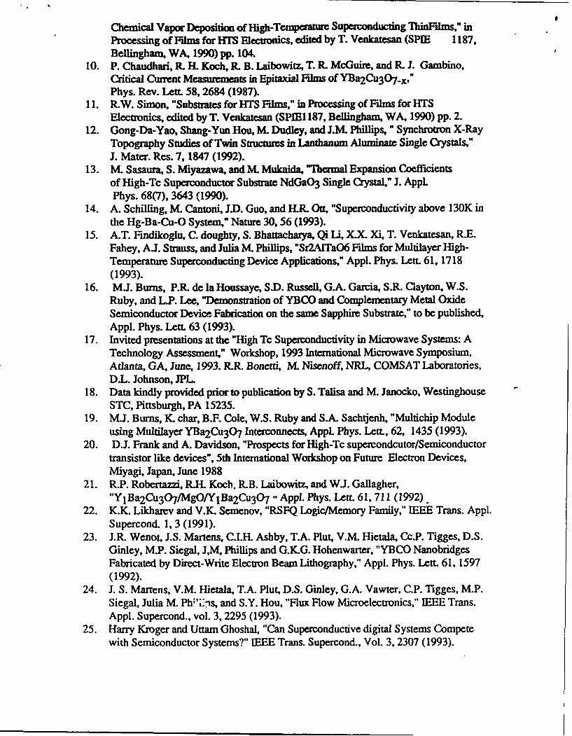
differentiation of film growth orientations (001) and (110)) ambiguous (vide infra ).Diffractometric rocking curves (o-scan) indicate a high degree of alignment/perfection ofthe film growth planes with respect to the substrate surface. Thus, the full width at halfmaximum (FWHM) of the YAIO 3 (004)t(220) reflection is 0.440 (Figure lb) versus 0.110for the corresponding (220) reflection of the single crystal substrate. A #-scan was alsoperformed to assess the quality of the in-plane epitaxy. In theory, four equivalent planes ofreflection should be observed, repeating every 88.370 or 91.630. A typical #-scan of the<202> family of diffraction planes (Figure Ic) exhibits the requisite two-fole (nearly four-fold) symmetry, hence a high level of in-plane epitaxy.
OAAI.-
0.0
1s 25 3 45 G's 73 Is209 (deums)
b....0. 1.0
0..0 . •b •_i • .I$A so Cl~ 441 P6 .
0.. .4 046
.0. 0.6
10.4. 0.4
0.2 0.2
0.01 0o.1•4 -2 0 2 4 0 90 IgO 270 WS (d~eu) * (dqwues)
Figure 1. X-ray diffrcion of an in $itu MOCYD-daived YAIO3 film on a LaAIO3 substrate.a. 0-20 scan, b. coscan of YAIO3 (004)/(220) reflection. The FWHM of thereflection is 0.44P, c. #-scan of <022> family of planes.
In-Situ Growth of PrGaO3 Thin Films
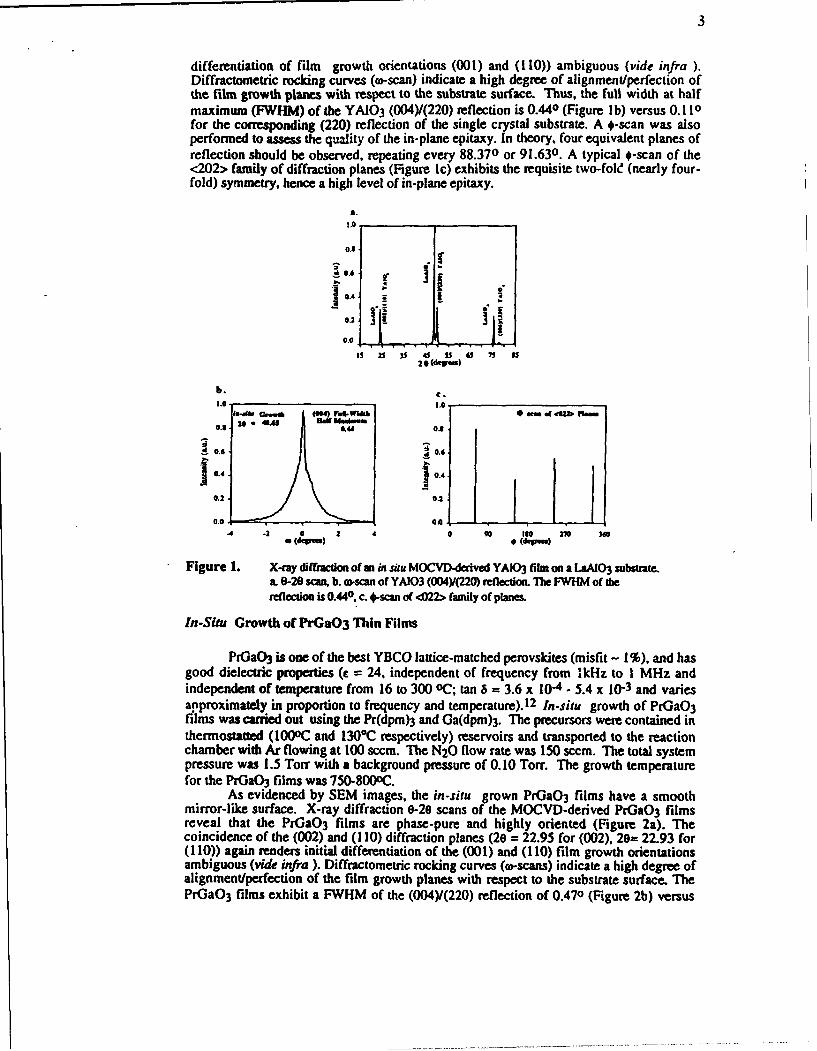
PrGaO3 is one of the best YBCO lattice-matched perovskites (misfit - 1%), and hasgood dielectric properties (c = 24, independent of frequency from 1kHz to I MHz andindependent of temperature from 16 to 300 °C; tan 6 = 3.6 x 10⁻⁴ - 5.4 x 10⁻³ and variesapproximately in proportion to frequency and temperature).1 2 In-Situ growth of PrGa0 3films was carried out using the Pr(dpm)3 and Ga(dpm)3. The precursors were contained inthermostatted (100oC and 130*C respectively) reservoirs and transported to the reactionchamber with Ar flowing at 100 sccm. The N20 flow rate was 150 sccm. The total systempressure was 1.5 Torr with a background pressure of 0.10 Torr. The growth temperaturefor the PrGaO3 films was 750-8000C.
As evidenced by SEM images, the in-situ grown PrGaO3 films have a smoothmirror-like surface. X-ray diffraction 0-20 scans of the MOCVD-derived PrGaO3 filmsreveal that the PrGaO3 films are phase-pure and highly oriented (Figure 2a). Thecoincidence of the (002) and (110) diffraction planes (20 = 22.95 for (002), 20= 22.93 for(110)) again renders initial differentiation of the (001) and (110) film growth orientationsambiguous (vide infra ). Diffractometric rocking curves (w-scans) indicate a high degree ofalignment/perfection of the film growth planes with respect to the substrate surface. ThePrGaO 3 films exhibit a FWHM of the (004)1(220) reflection of 0.470 (Figure 2b) versus

4
0. 110 for the corresponding (220) reflection of the LaAIO 3 substrate. In order to assess thequality of the in-plane epitaxy, #-scans were also performed. In theory, four equivalentplanes of reflection should be observed, repeating every 89.680 or 91.320. A typical #-scanof the <202> family of diffraction planes (Figure 2c) exhibits the requisite two-fold (nearlyfour-fold) symmetry and hence a high level of in-plane epitaxy.
a.1.0
0 t.,•u 0-*6•
0.9
I 0
0.4 -
t I0.2 "0
1S 25 35 M 55 73 52e (dewm)
b. c.
1.0 1.0
2It 41. as41 Mea.mOJ *.io 0.I
.4 0.4
0.2 0.2
0. 0. , ,
- .3 I I 3 5 -IO N IU0 No 3500a (1 ) *( i(
Figure 2. X-ray diffraction of an in situ MOCVD-derived PiGaO3 film on a LaAIO3 substrate.L 9-20 scan, b. n-scan of PaGaO3 (004)/(220) reflection. The FWHM of thereflection is 0 .500. c.. #scan of <022> family of planes.
The suitability of the MOCVD-derived PrGaO3 films as buffer layers for YBCOthin film growth has been demonstrated by pulsed laser deposition (PLD) 16 and pulsedorganometallic molecular beam epitaxy (POMBE) techniques.17 The YBCO films grownby PLD and POMBE on MOCVD-derived PrGaO3 exhibit Tc's of 91 and 89 K,respectively, and Jc'S of 6 x 10⁶ Alcmn2 at 77 K. These results indicate that MOCVD-derived PrGaO3 performs as a high quality buffer layer.
In Situ Growth of NdGaO3 Thin Films
NdGaO 3 is also a YBCO lattice-matched perovskite (misfit - 1%) with excellentdielectric properties (e = 22 at 3 GHz and 77 K; tan 6 - 3 x 10⁴ at 5 GHz and 77 K)2 5
Growth of NdGaO3 films was carried out in situ using the precursors of Nd(dpm)3 andGa(dpM)3. The sources were set at 100 OC and 140 OC for the Ga precursor and Ndprecursor respectively. Deposition of the film was carded out at a system pressure of 1.5Torr (background pressure = 0.1 Torr) and a substrate temperature of 800 oC. Flow ratesof 100 sccm for Ar and 300 sccm for N20 were routinely used.
X-ray diffraction 0-20 scans (Figure 3a) reveal that the films are phase-pure andhighly textured. The coincidence of (110) and (002) diffractioh planes again preventsinitial differentiation of (110) and (001) film growth orientation. X-ray diffraction rockingcurves were measured for the NdGaO3 films. The FWHM of the (220)1(004) NdGaO 3reflection is 0.480 as determined by a least-squares fitting method (Figure 3b), while theFWHM of the LaAIO 3 (220) substrate reflection is 0.110. X-ray diffraction # scans wereperformed to determine the quality of the in-plane epitaxy. In theory, four equivalent

S
planes spaced every 89.290 or 90.710 should be observed. A typical +-scan of the <202>diffraction planes for an MOCVD-derived NdGaO 3 film on LaAlO3 shows the requisite,two-fold (nearly four-fold) symmetry, which confirms a high level of in-plane epitaxy(Figure 3c).
0.
.01
0 ji5 25 35 5 55
20 (depnm)
b. C.1.0 1.0
(W) rFaW id th ofm . ObPIm a
0.8 20 "A.BC l *l 0.8.
S0.4 0.
0.2 .2
-5 -3 - I 3 ( ) (dewlm)
Figure 3. X-ray diffraction of an in situ MOCVD-derived NdGaO3 rIdm on a LSAIO3 substre.L 0-20 scan. b. w-scaD of NdG2O3 (004)/(220) reflection. The FWHM ofthereflection b 0.480, c. -scan of <022> family of planes.
In Situ Growth of Sr2AITaO6 Films
Sr2AlTaO6 (SAT) is particularly attractive as an insulating material for use in HTSelectronics since it exhibits a good lattice match with YBCO (- 2%) (Sr2AITaO 6 has acubic structure with ao = bo = co = 7.795 A;l8 YAIO3. PrGaO3 and NdGaO3 areorthorhombic), a very low reported dielectric constant (e = 11.8 at room temperature and100 K) and low dielectric loss (tan 6 = 1.68 x 10⁻³ and 4.24 x 10⁻³ at room temperature and100 K, respectively). 19 Furthermore, Sr2AITaO6 exhibits no phase transitions betweenroom temperature and 7500C. MOCVD of Sr2AITaO6 films was carried out in a horizontalmetal reactor using the metal-organic precursors Sr(hfa)2(tetraglyme), Al(acac)3, andTa2 (OCH2 CH3 )I0 as well as the reactant gas N20. The precursors were contained inthermostatted flasks at 60 oC, 90 oC, and 130 CC for the Ta. Al, and Sr precursors,respectively, and transported to the reaction chamber by Ar flowing at 60 - 100 sccm. TheN20 was introduced immediately upstream of the susceptor at a flow rate of 150-200 sccm.The total system pressure was 1.5 Torr with a background pressure of 0.10 Torr. Thesubstrates were heated restively at 750-900 eC during film depositions.
X-ray diffraction 0-2o scans of the MOCVD-derived Sr2AITaO6 films reveal a verylarge sensitivity of composition and microstructure to the deposition conditions. Filmsgrown at 750 CC are multi-phase and largely unoriented as indicated by 0-20 scans.20
Identified phases included Sr2AITaO6, SrF2, and SrALIO7. The source of fluoride iswithout doubt the hfa ligand. In contrast, films grown at 800 oC with all other conditionsidentical, yielded phase-pure Sr2AITaO6 films.20 Diffractometric rocking curves (.-scans)indicate a low degree of alignment/perfection of the film growth planes with respect to the

6
substrate surface. The films exhibit a FWHM for the Sr2AITaO6 (400) reflection of 2.030versus 0.20" for the corresponding (220) reflection of the LaAIO 3 single-crystalsubstrate.20 In-plane #-scans were also performed to assess the quality of the in-planeepitaxy. In theory, four equivalent planes of reflection should b6_ observed, repeating every900. Typical 4 scans of the <220> family of Sr2AITaO6 diffraction planes grown at 800 OCexhibits the requisite. four-fold symmetry, but with rather broad peaks. 20
Increasing the substrate temperature to 850 oC during deposition results insignificant enhancement of growth plane alignment and crystallinity (Figure 4a).Diffractometric rocking curves now exhibit a FWHM for the Sr2AITaO6 (400) reflection of0.51" (Figure 4b). Typical # scans of the <220> family of Sr2AITaO6 diffraction planes (Figure 4c) exhibit sharp reflections having the requisite four-fold symmetry and hence ahigh level of in-plane epitaxy.
a.
1.0
0.1
040
0.2 1
015 25 35 5 55 4 75
26 (dwp-4
b. C.1.0 3 .0.
(4m4) F.S.With[ o f . d ltb Paeý20 2 .- "isna Me.m me0
0o .0 0.02
1 0.4 10.4
0 0* (4qm.) @(q
Figure 4. X-ray diffraction of an in situ MOCVD-derived Sf2TaAIO6 film on a LaAIO3 substrate.a. 0-20 scan for the film grown a 850 0C. b. w-sc.n of (200) releation of Sr2TaAIO6grown it 850 "C. The FWHM of the rdlecon is 0.51P. c. #-scan of <022> family ofplanem for the fil, grown at 850 °C.
DISCUSSION
One common microstructural feature of the epitaxial PrGaO3, NdGaO3, and YAIO3films grown on LaAIO3 is epitaxial growth with two growth directions: <001> and <110>and three growth domains as observed by HREM images and TEM selected area diffraction(Figure 5). The same results were also observed by Brorsson et al.21 when the PrGaO3was grown on YBCO by laser ablation. The two growth orientation feature is determinedby the crystal structure. In the crystal structures of PrMaO 3, NdGaO 3 and YAIO 3 the unitlength in the unit cell in the <110> direction is very close to co ( co G ( ao2 + b0
2 )12 ). Bothgrowth orientations, <001> and <110>, have very close lattice mismatch properties witheither YBCO or LaAIO 3 on which the dielectric thin films were grown. This indicates thatthe two growth orientations are both favored for nucleation and growth at - 800 °C. Eventhough films of YAIO 3, PrGaO3, and NdGaO3 grow with two directions and three kinds ofdomains, the microstructures are close to perfectly aligned at the domain boundaries. This

7
observation means that the three domains exactly match each other at the domainboundaries. With respect to the growth of multilayer structures, a YBCO film can begrown epitaxially on the two coexistent orientations of the buffer films (Figure 5), becauseboth orientations have essentially the same lattice match with YBCO.
Fiur 5 a ros-ecina HfltimgeoraY~2C3OxPr3a~falOMIlae".1utu~b. I Seew-PAradfrcinpumoaYaCUO.lra3LAO larsrcu
b E.theeeto emi epniua otefl ufc~
8
CONCLUSIONS
Phase pure thin films of HTS lattice-matched and low dielectric constant and lowdielectric loss tangent perovskite insulators YAIO 3. PrGaO3, NdGaO3, and Sr2TaAIO 6have been grown in-situ on single-crystal (110) LaAIO3 substrates by metal-organicchemical vapor deposition (MOCVD). The films exhibit mirror-like smooth surfaces. Thefilms grow epitaxially as shown by X-ray diffraction. As assessed by the HREM images,the films grow with atomically abrupt film-substrate interfaces and the epitaxial growth isfurther confirmed. The feature of two coexisting growth orientations ( <001> and <110> )and three epitaxial growth domains is observed in the MOCVD-derived PrGa03, NdGaO 3,and YAIO 3 films. For Sr2TaAIO6, a growth temperature of 850DC is required in order toprepare phase pure epitaxial thin films.
ACKNOWLEDGMENT
This research was supported by the National Science Foundation through theScience and Technology Center for Superconductivity (Grant DMR 9120000) and theNorthwestern Materials Research center (Grant DMR 9120521) and by DARPA throughContract 91-C-0 112. We thank Dr. David A. Rudman, Mr. D. B. Buchholz, and Prof.R.P.H. Chang for growing YBCO films on the MOCVD-derived dielectric buffer films byPLD and POMBE, and Dr. Hong Zhang and Prof. V. P. Dravid for TEM analysis. Wethank Drs. G. Wagner and J. Talvacchio for stimulating discusstions.
REFERENCE
1. J. Talvacchio and G.R. Wagner, SPIE Proc. 1292:2 (1990), and references therein.2. W. Ito. S. Okayama. N. Homma. and T. Morishita, AppL Phys. Let. 62:312 (1993).3. K.H. Young and D.D. Srother, Physica C 208:1 (1993), and references therein.4. J.M. Philips, M.P. Siegal, R.B. Van Dover, T.H. Marshall, C.D. Brandle, G. Berkstrcsser, AJ.
Strauss, RE. Fahey, S. Sengupta, A. Cassanto, and H.P. Jenssen. J. Mater. Res. 7:2650 (1992).and references therein.
5. H. Haefke, H.P. Lang. R. Sum, HJ. Guntbeodt, L Berthold, and D. Hesse, Appi. Phys. Lett. 61:2359(1992).
6. S. Honstu, J. Ishii, and S. Kawai. Appl. Phys. Lem. 59:2886 (199 1), and references therein.7. G. Malandrino, D.S. Richeson, TJ. Madks, D.C. DeGroot, iL. Schindler, and C.R. Kannewud, Appl.
Phys. Lett. 58:182 (1991), and references therein.8. J. Zhao, Y.Z. Li, C.S. Chern, PItA, B. Norris. B. Gallois, F. Kear, XD. Casandey. R.E. Wu.
Muenchausen, and S.M. Garrison, Appl. Phys. Leu. 59:1254 (1991)X and references therein.9. K. Zhang. and A.Erbil, Materials Science Forum, in press, and references therein.10. F. Hirai and H. Yamane, J. Crystal Growth 107:683 (1991), and references therein.11. B. Han, D.A. Neumayer, D.L Schulz, BJ. Hinds, TJ. Marks, H.Zhang, and V.P. Dravid, Chem.
Mater. 5:14 (1993).12. M. Sasurau, . Mukaida, and S. Miyazawa. Appl Phys. Leu. 57: 2728 (1990) and references therein.13. HJ. Scheel, M. Berkowski and B. Chabot, J. Crystal Growth, 115:19(1991).14. G.W. Berkstresser, Al. Valentino. and C.D. Brandle, 1. Crystal Growth, 109:467 (1991).15. H. Aso0o, S. Kubo, 0. Michikawi, M. Saton and T. Konaka, Jpn. J. Appl. Phys. 29: L1452 (1990).16. B. Han, D.A. Neumayer, TJ. Marks, D.A. Rudman, H. Zhang, and V.P. Dravid, submitted to Appl.
Phys. Let.17. B. Han, D.A. Neumayer, TJ. Marks. D. B. Buchbolz, and R.P.H. Chang, unpublished results.18. C.D. Brandle and VJ. Fratello, J. Mater. Res. 5:2160 (1990).19. R. Gou, J. Sheen, A. S. Bballa, F. Ainger, EC. Subbarao, L.E. Cross. Defense Advanced Research
Projects Agency/Office of Naval Research Workshop on Subsurate materials for High TcSuperconductors, Williamsburg, VA, 5-7 February, 1992.
20. B.Han, D.A. Neumayer, B.H. Goodrean, Ti. Marks, H. Zhang, and V.P. Dravid, submitted toAppl. Phys. Lett.
21. G. Brorsson, P. A. Nilsson, E. Olsson. S. 7.- Wang. T. Scaeson, and M. Lo(gren, Appl. Phys. Let.61:486 (1992).

Synthesis and Metal Organic Chemical Vapor Deposition oftButyl Substituted Cyclopentadienyls of Barium.
Bruce H. Goodreau, Bruce J. Hinds, and Tobin J. Marks*
Contribution from the Department of Chemistry, the Materials Research Center, and the
Science and Technology Center for Superconductivity, Northwestern University,
Evanston, Illinois 60208
Metal Organic Chemical Vapor Deposition (MOCVD) of barium containing complex
oxide thin films requires the use of compounds with a high and stable vapor pressure. To
this end, Ba f0-diketonatesl and more recently 13-ketoiminates 2 have been used as volatile
molecular precursors for MOCVD of metal oxide thin films. The problem of low volatility
source compounds in Ba MOCVD is a result of the small charge to radius ratio of Ba+2 .
Ba(dpm)2 (dpm = dipivaloylmethane) suffers from compositional variation and
oligimerization as a result of the small charge to radius ratio .3a-c In the second generation
precursor, Ba(hfa)2-tetraglyme (hfa = hexafluoroacetylacetonate), oligimerization is
overcome through the use of highly electron withdrawing hfa- ligands which allow for the
coordination of tetraglyme thus saturating the coordination shell of barium resulting in an
increase in volatility over Ba(hfa)2 .4a,b BaF2 formation has been observed in thin films
derived from Ba(hfa)2-tetraglyme and often requires further processing steps to remove the
fluoride ions.4 a,5 The development of barium precursor compounds which overcome both
the problems of low volatility and BaF2 formation in thin films is critical to the
advancement of MOCVD of barium containing thin films. In order to achieve the desired
volatility and vapor pressure stability in a non-fluorinated group 2 metal complex, we have
begun investigating encapsulated barium metallocenes 6 as MOCVD precursor compounds.
This communication describes the synthesis and characterization of bis(ditbutylcyclo-

pentadienyl)barium (1) and bis(tritbutylcyclopentadienyl)barium (2) and their use as
volatile precursors for the growth of BaPbO3 thin films by MOCVD.
The synthesis of ditbutylcyclopentadiene and tritbutylcyclopentadiene was carried
out using the phase transfer catalyzed method of Vernier and Casserely.7 The ligands were
characterized by their 1H and 13C NMR spectra. The barium complexes were prepared by
stirring barium granules in ammonia gas saturated tetrahydrofuran with the appropriate
cyclopentadiene (see reaction 1).8 Compounds 1 and 2 ((CptBu2)2Ba and (CptBu3)2Ba
respectively) were isolated as base free white solids by sublimation of the crude reaction
product after filtration and solvent removal. (CptBu2)2Ba and (CptBu3)2Ba where
characterized by elemental analysis, infrared spectroscopy, IH NMR spectroscopy, 13C
NMR spectroscopy, and mass spectrometry.9 ,10
tBun ,/f d tBun
B a 0 2'B NH3+TF 2\ sublimation
'Bun
- H2 Ba -2THF - Ba
n=2 or 3 1 tBun -2TH-tBun (1)
The chemical and thermal properties of compound 2 suggested that it could be used
as MOCVD precursor compounds. Compounds 1 and 2 are both air and moisture
sensitive materials. (CptBu2)2Ba decomposes immediately upon exposure to the
atmosphere, while (CptBu3)2Ba only begins to decompose after five minutes. (CptBu2)2Ba
melted without decomposition from 3420 C-346*C while (CptBu3)2 Ba melted without
decomposition from 108*C-1 100C. Compounds 1 and 2 sublimed at 210'C and 120*C
respectively at 5x1O"6 Tort. The observations above reveal that (CptBu3)2Ba has a greater
degree of encapsulation of the barium atom than does (CptBu2)2Ba. The two additional
tertiary butyl groups on compound 2 have a marked effect on the physical properties of
these compounds. Hanusa has reported similiar changes in melting points and sublimation

temperatures to cyclopentadienyl group 2 metal complexes upon increasing the number of
isopropyl groups attached to the cyclopentadienly ring.6 a,b
The results of the thermogravimetric analysis (TGA) of (CptBu3) 2Ba is shown in
Figure 1 along with those for Ba(dpm)2 and Ba(hfa)2-tetraglyme for comparison. 11 From
the thermograms shown on Figure 1, it is evident that (CptBu3)2Ba is more volatile than
Ba(dpm)2 and only slightly less volatile than Ba(hfa)2-tetraglyme. The TGA trace for
(CptBu3) 2 Ba is much narrower than and shows much less residue than the TGA trace for
Ba(dpm)2. In terms of volatility and vapor pressure stability, (CptBu3) 2 Ba is superior to
Ba(dpm)2. In comparison to Ba(hfa)2-tetraglyme, (CptBu3) 2 Ba has a similar sublimation
onset temperature, but has a broader weight loss curve. While the volatility is slightly
below Ba(hfa)2-tetraglyme, (CptBu3)2Ba contains no fluorine thus alleviating the
possibility of BaF2 formation in thin films. All of these observations taken together
suggested that (CptBu3)2Ba could be useful as a fluorine free barium MOCVD source
compound.
MOCVD experiments were carried out in a hot walled low pressure quartz tube
MOCVD reactor and the resulting thin films were characterized by scanning electron
miscroscopy (SEM), elemental determination by x-ray analysis (EDX), x-ray photoelectron
spectroscopy (XPS), and x-ray diffraction (XRD). The (Cpt3u3)2Ba was placed in an
open ceramic crucible in the sublimation zone and heated externally. The substrate, yttria
stabilized zirconia or magnesium oxide, was mounted on a quartz holder in the deposition
zone which was also heated externally. The temperature of the substrate was monitored by
a thermocouple fed through to the back side of the substrate holder. The background
pressure of the system was 10-3 Torr. No carrier gas was used. Addition of an oxidizer
gas such as 02 caused the (CptBu3)2 Ba to decompose on the walls of the reactor in the
sublimation zone and in the crucible. In a typical experiment, the substrate was heated to
615'C and the sublimation zone was then heated to I 10C. The (CptBu3) 2Ba melted and
then was transported cleanly to the deposition zone. A small amount of (CptBu3) 2Ba

sublimed through the deposition zone and condensed on the walls of the reactor just
downstream of the deposition zone. After two hours a shiny grey metallic-like film coated
the walls of the reactor and the substrate. Analysis of the films by SEM/EDX and XPS
showed that they contained Ba and C, but the film was found to be amorphous by X-ray
diffraction. The Ba/C films were insoluble in acetone, water, HCI, and aqua regia.
Annealing the Ba/C film in PbO/02 at 900°C and one atmosphere for two hours yielded
polycrystalline BaPbO3 as shown by x-ray diffraction (Figure 2). A small amount of Ba0
remained in the BaPbO3 films even after repeated PbO/02 annealing. The observation of
Ba0 was quite remarkable considering the highly oxidizing conditions of the anneal. The
Bao might result from the formation of a BaPbO3 layer protecting small crystallites of Bao.
Analysis of the BaPbO3 film by XPS showed that in addition to Ba, Pb and, 0 the film
contained some carbon. The SEM image of the amorphous Ba/C film revealed that the
surface was very smooth while the surface the BaPbO3 was quite rough (Figure 3). Post
annealing procedures typically have this effect on film morphology. 12
We have demonstrated the ease in which compounds 1 and 2 can be synthesized by
the ammonia gas saturated tetrahydrofuran method. This method offers a very simple
alternative to the metathesis of BaI2 with K(CptBun) which requires the preparation and
purification of K(CptBun). (CptBu3)2Ba is a highly volatile and fluorine free MOCVD
precursor as evidenced by its use in the fabrication of BaPbO3 films. The essential
component which makes (CptBu3)2Ba a useful MOCVD precursor is the tri-
tbutylcyclopentadiene ligand. Tritbutylcyclopentadiene affords highly volatile thermally
stable barium compounds which are easily decomposed under MOCVD conditinns.
Further work is in progress to address the question of oxygen stability under the conditions
necessary for the in situ deposition of metal oxides.
Acknowledgments. This work was supported by DARPA (contract # 9 1-C-
0 112) administered by Westinghouse Electric Corp. We thank Northwestern University
Materials Research Center for access to x-ray diffraction facilities.

-E) (tBu3-CP)2 Ba
50 - 3Ba(hfa)2 (tetraglyme)
co 40-
30
20-
10-
100 200 300 400 500
Temperature (OC)
Figure 1. Thermograms of (Cp'Bu3)2Ba, Ba(dpm)2, and Ba(hfa)2-tetraglyme.

0-4
-41
L
C1
20 30 40 50 60
20
Figure 2. X-ray diffraction pattern of an MOCVD derived BaPbO3 film On MgO.

(a) (b)
Figure 3. SEM images of thin films derived from the MOCVD of (CptBu3)2Ba (a) amorphousBa/C film (b) BaPbO3 film.

References
1. Tong, L.M.; Richeson, D.S.; Marks, T.J.; Zhao, J.; Zhang, j.; Wessels, B.W.; Marcy, H.O.;
Kannewurf, C.R. Advances in Chemistry Series 1990 226, 351 and references therein.
2. Schulz, D.L.; Hinds, B.J.; Stem, C.L.; Marks, T.J. Inorg. Chem. 1993, 32, 249.
3. (a) Turnipseed, S.B.; Barkley, R.M.; Sievers, R.E.; Jnorg. Chem. 1991, 30, 1164. (b)Gleizes, A.; Sans-Lanain, S.; Medus, P.; Morancho, R.; C.R. Acad. Sci. Ser. 2, 1991 312,983. (c) Rossetto, G.; Polo, A.; Benetollo, F.; Porcia, M.; Zanella, P. Polyhedron, 1992, 11,979.
4. (a) Timmer, K.; Spee, C.I.M.A.; Mackor, A.; Meinema, H.A.; Spek, A.L.; Vandersluis, P.lnorg. Chima. Acta. 1991, 190, 109. (b) Schultz, D.L.; Neumeyer, D.; Marks, T.J. Inorg.Synth. submitted.
5. (a) Malandrino, G.; Richeson, D.S.; Marks, T.J.; DeGroot, D.C.; Schindler, U..; Kannewurf,C.R. Appl. Phys. Lett. 1991,5S8, 182. (b) Zhang, J.M.; Wessels, B.W.; Richeson, D.S.;Marks, T.J.; DeGroot, D.C.; Kannewurf, C.R. J. App!. Phys. 1991, 69, 2743. (c) Duray, S.J.;Buchholtz, D.B.; Song.S.N.; Richeson, D.S.; Ketterson, J.B.; Marks, T.J.; Chang, R.P.H.Appl. Phys. Lett. 19915S9 1503.
6. (a) Burkey, D.J.; Williams, R.A.; Hanusa, T.P. Organometallics 1993, 12, 1331. (b)Williams, R.A.; Tesh, K.F.; Hanusa, T.P. JI Ant. Chem. Soc. 1991,113, 4843.
7. Vernier, C. 0.; Casserly, E.W. J. Am. Chem. Soc. 1990, 112, 2808.
8. Drake, S.R.; Otway, D.J.; J. Chem. Soc. Chem. Comm. 1991, 517.
9. 69.5% yield. mp. 342*C-347*C. Anal, for C26H42Ba; Ca~c'd: 63.43% C, 8.60% H, Found:63.30% C, 8.67% H. 1H NMR (toluene d-8): 8 1.28 (s, 36H), 5.60 (br t, 2H, J-2Hz), 5.93 (d,4H, J=2.4Hz). 13C NMR (toluene d-8): 8 32.30 £(CH3)3, 33.03 C(CH3)3, 103.25 ring _CH,105.61 ring CH, 136.48 C-tBu. JR (Nujol mull): 3058 (w), 3063 )w, 1364 (s), 1353 (s),1250(s), 1199 (in), 1162 (in), 1050 (w), 1043 (w), 1017 (w), 933 (w), 802 (s), 782 (s), 730(s),687 (in), 673 (in), 663(m). Mass Spec. (El, 70 eV): 492 (M+ envelope, mass: obs.(calc) 489:9.0(9.7), 490: 13.5(13.1), 491: 13.5(13.1), 492: 100(100), 493: 27.9(28.4), 494: 2.1(4.0)), 410(M+ - HCC..tBu), 315 (M+ - CptBII2).
10. 10.6% yield. mp. 108'C-I10*C. Anal. for C34H58Ba; Calc'd: 67.59% C, 9.68% H, Found:67.68% C, 9.66% H. 1H NMR (toluene d-8): 6 1.28 (s, 18H), 1.38 (s, 36H), 5.78 (s, 4H).13 C NMR (toluene d-8): 8 32.11 Q(CH3)3, 33.03 C(-CH3)3, 33.60 £(CH3)3, 34.66 C(-CH3)3,108.42 ring _CH, 130.36 ring _C-tBu, 132.53 ring _£-tBu. JR (Nujol mull): 3093 (w), 3078(w),1385 (mn), 1363 (in), 1355 (s), 1237 (s), 1195 (w), 1160 (w) 1002 (w), 790 (s), 675 (w). MassSpec. (El, 70 eV): 604 (M+ envelope, inass:obs(calc.), 601:8.7(9.8), 602:13.2(13.7),603:17.6(19.2), 604:100(100), 605:34.8(36.8), 606:5.3(6.7)), 371 (M+ - CptBu3)
11. Han, B.; Neumayer, D.; Schulz, D.L.; Marks, T.J.; Zhang, H.; Dravid, V.P. Appi. Phys.Lett., in press.