professor ralph mason fall term 2000 - university of ottawarabielmo/proknet/final_report.pdf ·...
TRANSCRIPT

Proknet c©: Not your average IP over
ATM segmenter
Submitted in partial fulfillment of the requirements for 97.584:
VLSI Design
Professor Ralph Mason
Fall Term 2000
Wael Hermas†Rami Abielmona†
Mohamed Abou-Gabal†
†(whermas,rabiel,mabou)@doe.carleton.ca
December 10, 2000

2

Contents
I Preface 130.1 Abstract . . . . . . . . . . . . . . . . . . . . . . . . . . . . . . 150.2 List of Acronyms . . . . . . . . . . . . . . . . . . . . . . . . . 16
II Introductions 17
1 IP over ATM 191.1 Segmentation Theory . . . . . . . . . . . . . . . . . . . . . . . 211.2 AAL Protocols . . . . . . . . . . . . . . . . . . . . . . . . . . 211.3 ATM Adaptation Layer 5 . . . . . . . . . . . . . . . . . . . . 22
1.3.1 The CPCS within AAL5 . . . . . . . . . . . . . . . . . 23
2 System Architecture 25
III Module design 31
3 TLL module design 333.1 Top Level . . . . . . . . . . . . . . . . . . . . . . . . . . . . . 33
3.1.1 Theory . . . . . . . . . . . . . . . . . . . . . . . . . . 333.1.2 Design History . . . . . . . . . . . . . . . . . . . . . . 343.1.3 Functional and Hardware Specifications . . . . . . . . 353.1.4 Functional Simulation . . . . . . . . . . . . . . . . . . 363.1.5 Synthesis . . . . . . . . . . . . . . . . . . . . . . . . . 373.1.6 Timing Simulation . . . . . . . . . . . . . . . . . . . . 37
3.2 Counter . . . . . . . . . . . . . . . . . . . . . . . . . . . . . . 383.2.1 Theory . . . . . . . . . . . . . . . . . . . . . . . . . . 383.2.2 Functional Specification . . . . . . . . . . . . . . . . . 383.2.3 Hardware Specification . . . . . . . . . . . . . . . . . . 423.2.4 Functional Simulation . . . . . . . . . . . . . . . . . . 47
3

4 CONTENTS
3.2.5 Synthesis . . . . . . . . . . . . . . . . . . . . . . . . . 483.2.6 Timing Simulation . . . . . . . . . . . . . . . . . . . . 49
3.3 Extractor . . . . . . . . . . . . . . . . . . . . . . . . . . . . . 493.3.1 Functional Specification . . . . . . . . . . . . . . . . . 493.3.2 Hardware Specification . . . . . . . . . . . . . . . . . . 503.3.3 Functional Simulation . . . . . . . . . . . . . . . . . . 503.3.4 Synthesis . . . . . . . . . . . . . . . . . . . . . . . . . 523.3.5 Timing Simulation . . . . . . . . . . . . . . . . . . . . 52
3.4 Padder . . . . . . . . . . . . . . . . . . . . . . . . . . . . . . . 533.4.1 Functional Specification . . . . . . . . . . . . . . . . . 563.4.2 Hardware Specification . . . . . . . . . . . . . . . . . . 583.4.3 Functional Simulation . . . . . . . . . . . . . . . . . . 603.4.4 Synthesis . . . . . . . . . . . . . . . . . . . . . . . . . 61
3.5 ALU . . . . . . . . . . . . . . . . . . . . . . . . . . . . . . . . 613.5.1 Theory . . . . . . . . . . . . . . . . . . . . . . . . . . 613.5.2 Design History . . . . . . . . . . . . . . . . . . . . . . 623.5.3 Functional Specification . . . . . . . . . . . . . . . . . 643.5.4 Hardware Specification . . . . . . . . . . . . . . . . . . 653.5.5 Functional Simulation . . . . . . . . . . . . . . . . . . 653.5.6 Synthesis . . . . . . . . . . . . . . . . . . . . . . . . . 663.5.7 Timing Simulation . . . . . . . . . . . . . . . . . . . . 66
3.6 Accumulator . . . . . . . . . . . . . . . . . . . . . . . . . . . 663.6.1 Theory . . . . . . . . . . . . . . . . . . . . . . . . . . 663.6.2 Functional Specification . . . . . . . . . . . . . . . . . 66
4 FIFO module design 754.1 Theory . . . . . . . . . . . . . . . . . . . . . . . . . . . . . . . 754.2 Functional Specification . . . . . . . . . . . . . . . . . . . . . 754.3 Hardware Specification . . . . . . . . . . . . . . . . . . . . . . 774.4 Functional Simulation . . . . . . . . . . . . . . . . . . . . . . 794.5 Synthesis . . . . . . . . . . . . . . . . . . . . . . . . . . . . . 794.6 Timing Simulation . . . . . . . . . . . . . . . . . . . . . . . . 79
5 Trailer module design 815.1 Theory . . . . . . . . . . . . . . . . . . . . . . . . . . . . . . . 815.2 Functional Specification . . . . . . . . . . . . . . . . . . . . . 82
5.2.1 Trailer I/O . . . . . . . . . . . . . . . . . . . . . . . . 825.2.2 Trailer Operation . . . . . . . . . . . . . . . . . . . . . 83
5.3 Hardware Specification . . . . . . . . . . . . . . . . . . . . . . 845.4 Functional Simulation . . . . . . . . . . . . . . . . . . . . . . 85

CONTENTS 5
5.5 Synthesis . . . . . . . . . . . . . . . . . . . . . . . . . . . . . 865.6 Timing Simulation . . . . . . . . . . . . . . . . . . . . . . . . 86
6 CRC module design 876.1 Theory . . . . . . . . . . . . . . . . . . . . . . . . . . . . . . . 87
6.1.1 Byte-wise CRC . . . . . . . . . . . . . . . . . . . . . . 906.2 Functional Specification . . . . . . . . . . . . . . . . . . . . . 92
6.2.1 CRC Components and Operation . . . . . . . . . . . . 946.3 Hardware Specification . . . . . . . . . . . . . . . . . . . . . . 946.4 Functional Simulation . . . . . . . . . . . . . . . . . . . . . . 976.5 Synthesis . . . . . . . . . . . . . . . . . . . . . . . . . . . . . 976.6 Timing Simulation . . . . . . . . . . . . . . . . . . . . . . . . 97
7 SAR module design 997.1 Functional Specification . . . . . . . . . . . . . . . . . . . . . 997.2 Hardware Specification . . . . . . . . . . . . . . . . . . . . . . 1017.3 Functional Simulation . . . . . . . . . . . . . . . . . . . . . . 1027.4 Synthesis . . . . . . . . . . . . . . . . . . . . . . . . . . . . . 1047.5 Timing Simulation . . . . . . . . . . . . . . . . . . . . . . . . 105
8 Microprocessor Module Design 1078.1 Theory . . . . . . . . . . . . . . . . . . . . . . . . . . . . . . . 1078.2 Design history . . . . . . . . . . . . . . . . . . . . . . . . . . . 1108.3 Functional Specification . . . . . . . . . . . . . . . . . . . . . 116
8.3.1 Instruction Set . . . . . . . . . . . . . . . . . . . . . . 1168.3.2 Memory Interface . . . . . . . . . . . . . . . . . . . . . 1188.3.3 Control Units . . . . . . . . . . . . . . . . . . . . . . . 121
8.4 Hardware Specification . . . . . . . . . . . . . . . . . . . . . . 1258.5 Functional Simulation . . . . . . . . . . . . . . . . . . . . . . 1268.6 Synthesis . . . . . . . . . . . . . . . . . . . . . . . . . . . . . 1278.7 Timing Simulation . . . . . . . . . . . . . . . . . . . . . . . . 128
9 Memory Module Design 1299.1 Theory . . . . . . . . . . . . . . . . . . . . . . . . . . . . . . . 1299.2 Design History . . . . . . . . . . . . . . . . . . . . . . . . . . 1309.3 Functional Specification . . . . . . . . . . . . . . . . . . . . . 1329.4 Hardware Specification . . . . . . . . . . . . . . . . . . . . . . 1339.5 Functional Simulation . . . . . . . . . . . . . . . . . . . . . . 1359.6 Synthesis . . . . . . . . . . . . . . . . . . . . . . . . . . . . . 1359.7 Timing Simulation . . . . . . . . . . . . . . . . . . . . . . . . 136

6 CONTENTS
IV Conclusions 137
10 System Integration 13910.1 Proknet c©in all its might . . . . . . . . . . . . . . . . . . . . . 139
10.1.1 System Integration . . . . . . . . . . . . . . . . . . . . 13910.1.2 Functional and Hardware Specification . . . . . . . . . 13910.1.3 Functional Simulation . . . . . . . . . . . . . . . . . . 13910.1.4 Synthesis . . . . . . . . . . . . . . . . . . . . . . . . . 141
10.2 Proknet c©limitations . . . . . . . . . . . . . . . . . . . . . . . 14110.3 Future Work . . . . . . . . . . . . . . . . . . . . . . . . . . . 14310.4 Project Conclusions . . . . . . . . . . . . . . . . . . . . . . . 143
A A - TLL module 147
B B - Trailer module 149
C C - CRC module 151
D D - Microprocessor module 153
E E - Memory module 155
F F - SAR module 157
G G - System Integration 159
H H - Design Documents 161
I I - Project Presentation 163

List of Figures
1.1 IP packet . . . . . . . . . . . . . . . . . . . . . . . . . . . . . 201.2 ATM cell . . . . . . . . . . . . . . . . . . . . . . . . . . . . . 211.3 ATM protocol reference model . . . . . . . . . . . . . . . . . 221.4 AAL type 5 CPCS PDU . . . . . . . . . . . . . . . . . . . . . 23
2.1 Preliminary system architecture . . . . . . . . . . . . . . . . . 262.2 Intermediate system architecture . . . . . . . . . . . . . . . . 272.3 Pre-final system architecture . . . . . . . . . . . . . . . . . . 282.4 Final system architecture . . . . . . . . . . . . . . . . . . . . 292.5 System breakdown . . . . . . . . . . . . . . . . . . . . . . . . 30
3.1 IP packet header . . . . . . . . . . . . . . . . . . . . . . . . . 333.2 TLR storage . . . . . . . . . . . . . . . . . . . . . . . . . . . 353.3 TLR/extractor algorithm . . . . . . . . . . . . . . . . . . . . 363.4 TLR/extractor circuit . . . . . . . . . . . . . . . . . . . . . . 373.5 Initial counter algorithm . . . . . . . . . . . . . . . . . . . . . 393.6 Initial counter implementation . . . . . . . . . . . . . . . . . 403.7 ASM chart . . . . . . . . . . . . . . . . . . . . . . . . . . . . 413.8 Data path . . . . . . . . . . . . . . . . . . . . . . . . . . . . . 413.9 Detailed ASM chart . . . . . . . . . . . . . . . . . . . . . . . 423.10 Control path . . . . . . . . . . . . . . . . . . . . . . . . . . . 433.11 Status signal . . . . . . . . . . . . . . . . . . . . . . . . . . . 433.12 XOR tree . . . . . . . . . . . . . . . . . . . . . . . . . . . . . 443.13 Ripple binary up counter . . . . . . . . . . . . . . . . . . . . 453.14 Data path of the counter module . . . . . . . . . . . . . . . . 463.15 Control path of the counter module . . . . . . . . . . . . . . . 473.16 Counter module architecture . . . . . . . . . . . . . . . . . . 473.17 Extractor architecture . . . . . . . . . . . . . . . . . . . . . . 513.18 First approach to padder algorithm . . . . . . . . . . . . . . . 543.19 Next-generation approach to padder algorithm . . . . . . . . 55
7

8 LIST OF FIGURES
3.20 Padder logic operations . . . . . . . . . . . . . . . . . . . . . 673.21 Padder operations using the register method . . . . . . . . . . 683.22 Padder algorithm . . . . . . . . . . . . . . . . . . . . . . . . . 693.23 Control path using gates . . . . . . . . . . . . . . . . . . . . . 703.24 Flip-flops of the 7 states of the control path . . . . . . . . . . 713.25 Comparator circuitry . . . . . . . . . . . . . . . . . . . . . . . 723.26 Full adder circuitry . . . . . . . . . . . . . . . . . . . . . . . . 723.27 Full adder-subtractor circuitry . . . . . . . . . . . . . . . . . 73
4.1 I/O of the FIFO module . . . . . . . . . . . . . . . . . . . . . 754.2 FIFO module architecture . . . . . . . . . . . . . . . . . . . . 764.3 FIFO control logic design . . . . . . . . . . . . . . . . . . . . 784.4 Comparator design . . . . . . . . . . . . . . . . . . . . . . . . 784.5 FIFO memory design . . . . . . . . . . . . . . . . . . . . . . . 80
5.1 Trailer overview . . . . . . . . . . . . . . . . . . . . . . . . . . 815.2 Packet in memory . . . . . . . . . . . . . . . . . . . . . . . . 825.3 Trailer field initializations . . . . . . . . . . . . . . . . . . . . 825.4 I/O of the trailer module . . . . . . . . . . . . . . . . . . . . 835.5 Trailer module architecture . . . . . . . . . . . . . . . . . . . 845.6 2 to 1 input multiplexer . . . . . . . . . . . . . . . . . . . . . 85
6.1 Logic circuitry . . . . . . . . . . . . . . . . . . . . . . . . . . 896.2 Transmitted message . . . . . . . . . . . . . . . . . . . . . . . 906.3 I/O of CRC module . . . . . . . . . . . . . . . . . . . . . . . 926.4 CRC module architecture . . . . . . . . . . . . . . . . . . . . 936.5 4 to 1 multiplexer . . . . . . . . . . . . . . . . . . . . . . . . . 956.6 CRC-32 overall design . . . . . . . . . . . . . . . . . . . . . . 96
7.1 Start counting and corresponding flip-flop . . . . . . . . . . . 1027.2 SAR FSM . . . . . . . . . . . . . . . . . . . . . . . . . . . . . 103
8.1 Microprocessor general architecture . . . . . . . . . . . . . . . 1088.2 Execution state machine . . . . . . . . . . . . . . . . . . . . . 1108.3 Initial pipeline design . . . . . . . . . . . . . . . . . . . . . . 1118.4 Initial memory interface . . . . . . . . . . . . . . . . . . . . . 1148.5 Initial memory map . . . . . . . . . . . . . . . . . . . . . . . 1158.6 Final memory interface . . . . . . . . . . . . . . . . . . . . . . 1208.7 PC architecture . . . . . . . . . . . . . . . . . . . . . . . . . . 1208.8 WAR architecture . . . . . . . . . . . . . . . . . . . . . . . . 1218.9 RAR architecture . . . . . . . . . . . . . . . . . . . . . . . . . 121

LIST OF FIGURES 9
8.10 ICU FSM . . . . . . . . . . . . . . . . . . . . . . . . . . . . . 1228.11 ACU FSM . . . . . . . . . . . . . . . . . . . . . . . . . . . . . 1238.12 MCU FSM . . . . . . . . . . . . . . . . . . . . . . . . . . . . 126
9.1 RAM cell . . . . . . . . . . . . . . . . . . . . . . . . . . . . . 1329.2 Final memory map . . . . . . . . . . . . . . . . . . . . . . . . 1339.3 Micro-CPU address decoding . . . . . . . . . . . . . . . . . . 134

10 LIST OF FIGURES

List of Tables
3.1 Comparator circuit truth table . . . . . . . . . . . . . . . . . 633.2 Full Adder circuit truth table . . . . . . . . . . . . . . . . . . 64
4.1 Truth table for address decoder . . . . . . . . . . . . . . . . . 79
6.1 CRC algorithm . . . . . . . . . . . . . . . . . . . . . . . . . . 886.2 CRC example . . . . . . . . . . . . . . . . . . . . . . . . . . . 906.3 CRC equation calculations (Most significant 16 bits) . . . . . 916.4 CRC equation calculations (Least significant 16 bits) . . . . . 91
8.1 Instruction set encoding . . . . . . . . . . . . . . . . . . . . . 1178.2 Final instruction set . . . . . . . . . . . . . . . . . . . . . . . 118
11

12 LIST OF TABLES

Part I
Preface
13


0.1. ABSTRACT 15
0.1 Abstract
This project presents Proknet c©. It is a play on the following words: networkand processor. It represents a module that is capable of receiving incom-ing variable-sized IP packets, and outputting fixed-sized ATM cells. Theapplications of this module are numerous, especially in the communicationsfield, where this type of circuit is needed in order to implement the ATMforum specifications. The following report is presented in a book fashion,in order to clearly dissect all of the tasks that were delegated and accom-plished by the designers. To be specific, any TLL- or SAR-related work isaccredited to Wael Hermas, any trailer- or CRC- related work is accred-ited to Mohamed Abou-Gabal, and any micro-processor/memory- or ALU-related work is accredited to Rami Abielmona. Appendices are included inthis report presenting the different modules and their corresponding sourceand output files (Verilog code, functional/timing simulation diagrams, andsynthesis outputs). Finally, attached to this report is a CD (also see Ap-pendix I), which contains all of module related work and a PowerPoint2000 (Microsoft c©) lasting approximately 5 minutes. This presentation isan overview of the overall system architecture and operation. Take a fewminutes and view the presentation (as a slide show) in order to get familiarwith the many topics that are discussed in this report.

16
0.2 List of Acronyms
AAL ATM Adaptation LayerACC AccumulatorACU Address Control UnitALU Arithmetic/Logic UnitAR Address RegisterAR Flip-flop Asynchronous Reset
ARSE Flip-flop Asynchronous Reset and Synchronous EnableAS Flip-flop Asynchronous Set
ASM Algorithmic State MachineATM Asynchronous Transfer ModeCISC Complex Instruction Set ComputerCPCS Common Part Convergence SublayerCPE Customer Premise EquipmentCPU Central Processing UnitCRC Cyclic Redundancy CheckCS Chip Select
DPRAM Dual-Port RAMEOP End of PacketFAS Full Adder-SubtractorFF Flip-flop
FIFO First-in First-outFSM Finite State MachineICU Instruction Control UnitIP Internet ProtocolIR Instruction Register
MCU Main Control UnitOSI Open System InterconnectionPC Program Counter
PDU Protocol Data UnitPR Pad Register
RAM Random Access MemoryRAR Read Address RegisterROM Read-Only MemoryRISC Reduced Instruction Set ComputerSAP Service Access PointSAR Segmentation and ReassemblySP Stack Pointer
SPR Special Purpose RegisterSSCS Service Specific Convergence Sublayer
TPRAM Ternary-Port RAMTLL Total Length LogicTLR Total Length Register
VLIW Very Long Instruction WordWAR Write Address Register

Part II
Introductions
17


Chapter 1
IP over ATM
The Internet has become one of the most diverse, information-filled librarythis century has ever seen, since the library of the U.S Congress. Its contentsrange from a variety of different topics, some of which include education,information, leisure and entertainment, as well as research and development.As the Internet becomes more reliable even on a daily basis, we are evolvingto be more dependent on its various tools and services. Our dependencyhence increases our awareness of the Internet, which in its turn leads tocustomers demanding more diverse and tailored services that they can mapto their everyday lives. This demand drives he emergence of new technolo-gies as well as the refinement of old ones in ways never thought possiblebefore. Two of the leading technologies that have surfaced are the Inter-net Protocol (IP), and Asynchronous Transfer mode (ATM). Thereare many differences between the two communication protocols, but due tothe scope of this document, only a few will be highlighted for clarity. TheIP communication protocol utilizes connectionless-based datagrams that arerouted using hop-by-hop routing algorithms to transfer information, whileATM utilizes connection-based cells that are guided using a pre-plannedpath between nodes. The main difference between the two is the processingpower required by both as well as the reliability offered by both protocols.As shown in figure 1.1, the total length of the packet is variable rangingfrom 20 bytes to as big as 65,536 bytes. The datagram approach is bestsuited for this type of routing methodology because each packet is treatedindependently, with no reference to packets that are gone before it. Dif-ferent packets may thus end up selecting different routes depending on thenetwork’s current status, and thus may end up arriving at the destinationin different orders. Neither error control nor any reliability mechanisms are
19

20 CHAPTER 1. IP OVER ATM
exercised in this protocol, which allows for the transmission of such variablesized packets, yet routing of every single packet is required which consumesgreater processing power. Now referring to figure 1.2, the total length of anATM cell is fixed at 53 bytes in total. The cell approach is alternatively bestsuited for this type of routing methodology because each packet is guidedvia a pre-planned route, where each cell traverses the dedicated route forthe entire length of data transmission. With this scenario, error control andreliability mechanisms are provided on a connection basis rather than a cellbasis, which reduces the processing power required by each node.
Figure 1.1: IP packet
Currently though, as a result of different amalgamated services, more andmore packet-switching networks have been making use of the more reliablecell-switching networks. The benefit from both technologies hence improvedthe different service provider’s delivered products. This allowed networksaround the world to present a service that is as reliable and dedicated asATM, while utilizing IP’s greater transmission capability and reduced over-head in terms of route setups. Out of this concept transpired the migra-tion of networks to offer IP over ATM. As described above, this protocoluses both technologies to deliver data, voice and video from one CustomerPremise Equipment (CPE) to another CPE and ultimately to the userthat desires this service. In order to be able to transmit variable-sized IPpackets over a fixed-cell ATM network, we have to be able to segment the IP

1.1. SEGMENTATION THEORY 21
packets into 48-byte cells at the transmitter, and be also able to reassemblethese same cells into the original packet at the receiver. Thus, this is goingto be the focus of this project and the discussion of Segmentation andReassembly (SAR).
Figure 1.2: ATM cell
1.1 Segmentation Theory
Figure 1.3 refers to the Open System Interconnection (OSI) modeldeveloped by ISO as a model for computer communications architecture.Within the ATM reference model, the ATM Adaptation Layer (AAL)has the ability to provide a transitional layer between the ATM layer andthe higher protocols. This allows for an enhancement of services providedby the ATM layer to all the higher level layers, which in our case is IP. Thefunctions performed by the AAL depend on the higher layer requirements.
1.2 AAL Protocols
There are different types of protocols that AAL supports in order to meetthe variety of needs of the higher layers, which are all defined under fourclasses of service that cover a broad range of requirements. The classificationis based on whether the application requires timing between the source and

22 CHAPTER 1. IP OVER ATM
Figure 1.3: ATM protocol reference model
destination, whether it requires a constant bit rate for traffic, and finallywhether it is a connection-oriented or connection-less transfer. Based on thiscriterion for classes of service, ITU-T defined four different AAL protocolsthat classify the operation the AAL based on each class of service [Hal92].As mentioned in figure 1.3, the AAL is made up of two logical sub layers: theConvergence Sub layer (CS) and the Segmentation And Reassemblysub layer. The convergence sub layer is needed to provide functions forspecific applications that are using the AAL. Higher protocols attach to theAAL by using a Service Access Point (SAP), which is the address of theapplication. This makes the CS a service dependent layer.
The SAR sub layer is then required to accept information from the CSwhile molding them into cells that are acceptable for transmission by theATM layer, as well as doing the opposite upon reception of cells from theATM layer at the other end. As mentioned above, the ATM layer can onlyaccept a 48-byte payload. Thus the SAR has to group any SAR headersand/or trailers as well as the CS payload into 48-byte cells ready for pro-cessing by the ATM layer.
1.3 ATM Adaptation Layer 5
Thus, for our IP application, the characteristics are that timing is not re-quired between the source and the destination, the bit rate is variable, and

1.3. ATM ADAPTATION LAYER 5 23
it is a connection-less transfer. This classifies IP as a class D application,which entails the utilization of the type 5 AAL protocol, which is a newly de-fined protocol. Like all other AALs, the higher layer protocols send a blockof data to the CS, which encapsulates them into Protocol Data Units(PDU) [Tan96]. Actually, the CS is referred to as the Common PartConvergence Sub layer (CPCS), making this layer in the CS the onethat performs common functions for the higher protocols, while the ServiceSpecific Convergence Sub layer (SSCS) performs the service specificoperations depending on which AAL is being utilized at the time by thehigher layer protocols based on their application.
1.3.1 The CPCS within AAL5
The function of the CPCS is very limited in for layer 5, in contrast withlayer 3/4 which has a more involved role in the AAL. CPCS takes on mostof the functions as the one used in layer 3/4, but with the difference ofexclusively providing error protection without the involvement of the SAR,as well as not giving a buffer allocation size indication to the receiving peerentity. Mainly, the CPCS is responsible for the following functions as showin figure 1.4 [Pry95]:
Figure 1.4: AAL type 5 CPCS PDU
• Padding (Pad) field This field allows the CPCS PDU total length tobe a multiple of 48, aligning it with the cell-size of an ATM cell. Itssize varies from 0 to 47 bytes.
• User to User field (UU) This field is used transparently between theAAL5 CPCS users, containing 1 byte of information

24 CHAPTER 1. IP OVER ATM
• Common Part Identifier (CPI) This field contains zeros at the moment,indicating that there are user data in the payload field.
• Length field This field indicates the length of the CPCS PDU payloadstored in the CPCS PDU. This is required in order to determine thesize of the pad field. The size length field varies from 0 to 2 bytes,which represents the size of the payload. As well, of note here is thatthe total length of an IP packet also varies from 16 bytes (header) to65535 bytes.
• CRC-32 field This field contains the CRC-32 calculation, which is doneover the entire CPCS PDU, including the payload, the pad, and theCPCS-PDU trailer in entire contents.
The polynomial used to generate CRC-32 is the following:
G(x) = x32+x26+x23+x22+x16+x12+x11+x10+x8+x7+x5+x4+x2+x+1(1.1)

Chapter 2
System Architecture
The main goal of this project is to provide an IP over ATM segmentationentity, that will accept a variable-sized IP packet, and transform it intofixed-sized ATM cells. To perform this goal, it was necessary to select abase architecture, that will aid us in the design and implementation phases.This task was not taken lightly as it will influence many future design aspectsand decisions. The system architecture has to present to the designer themain components, their interconnections and their operations. That said,the system architecture is not going to present the internal implementationdetails of any component, leaving it up to the imagination and innovationof the designer to design a functionally correct system. For this project,the system architecture went through quite a few design cycles before itseventual hardened declaration. The fact that the architecture is presentedfirst in this document is due its vitality for a smooth module design transi-tion. The drawbacks of ”hard-coding” the circuit to match the underlyingarchitecture are numerous, and expensive in terms of design cycles. Otherpitfalls of a bad system architecture are work-arounds implemented in orderto do exactly that: work around a system bug. On the other hand, a wellthought-out architecture will provide a baseline for all designers to reviewand synchronize to.
The system architecture started out with a basic design involving all thefunctions needed for a SAR entity (segmentation only in this case). Pleaserefer to figure 2.1 for the first design done. This design is very preliminaryand did not include many of the details of the correct system operation. Itdoes present, however, the goals of the project, the inputs and outputs ofthe system, and the high-level data flow. On the other hand, the design ismissing quite a few important aspects, such as appending a trailer after each
25

26 CHAPTER 2. SYSTEM ARCHITECTURE
IP packet. The design does not also take into effect which module shouldperform what operation. For that matter, the design does not even breakdown the system into different modules. As a first design, it is quite conciseand presents the idea in an orderly matter.
Figure 2.1: Preliminary system architecture
The next design is a CPU-intensive design, as seen in figure 2.2. This ar-chitecture plays very nicely into the re-programmability aspect of hardwaredesign. The CPU sequentially performs its functions. The throughput of thedesign is considered to be low due to the intense CPU-memory interaction insending completed packets to the SAR module. What this design presentsis a breakdown of the system into components. The architecture also clearlyshows the datapath as well as the system inputs and outputs. The architec-ture also defines some previously mysterious interactions between differentlogical components, as well as the inputs and outputs of each of the modules.As time went on, the design was modified in order to attempt to speed upthe processing throughput.
An intermediate design that was briefly considered involved each of themodules shown in figure 2.2 interacting with the memory unit. This designallowed for multiple packets to be processed simultaneously, but requiredthe use of a large multiport RAM and thus was instantly scrapped.
The final system architecture involved a pipelined design from start toend. There are two actual pipelines, an input and an output pipeline. Pleaserefer to figure 2.3 for a clearer picture of the following discussion. Theinput pipeline contains the TLL module, the CRC module and the trailermodule, while the output pipeline contains the SAR module. Sandwiched in

27
Figure 2.2: Intermediate system architecture
between both pipelines are the CPU and the memory modules, which linkthe output of the input pipeline to the input of the output pipeline. Thepipelined design allows us to handle multiple packets simultaneously withoutthe need for much external RAM. Each module is able to operate accordingto specification on the IP packet, as frames are transferred, byte-by-byte,through the pipeline (1 byte/1 clock cycle). Other advantages to this designis that each module views the whole packet one byte at a time, and hencepacket processing time is minimized. The whole architecture seems to beoperating in a parallel fashion, while latency and throughput are minimizedand maximized, respectively. One final issue is that the CPU is left to handlenon-data-intensive tasks, and thus memory interaction is also reduced.
The reasons for adding the total length logic (TLL) module on thepipeline are to find the total length of the IP packet, and setting the resultinto the total length (TL) register. The TLL also calculates the numberof bytes (assuming they are zeros) needed to be used in padding. The latteris done by setting the padding register (PR). The pipeline processes are

28 CHAPTER 2. SYSTEM ARCHITECTURE
Figure 2.3: Pre-final system architecture
data intensive that do not present any delays. The modules on the pipelineare the ones which require control signals (from a control unit).
What follows are a few of the design reviews that were performed tothe final system architecture, and are included here as is, in order to give areality aspect to the project:
October 9th - Design Re-engineer(DR): The padding algo-rithm/module should be moved to a different position on thepipeline. The ”Padding” should be implemented right after ”TLL”and before ”CRC”. ”Padding” was moved around like this be-cause we did not take into consideration of why ”padding” wasplaced right after ”Append T Trailer”. The only reason whyis that we just switched ”queuing” and ”padding” from the CPUmodule. The other reason of why it makes sense to put it af-ter TLL is because the way CRC is calculated. CRC needs tobe done on all the bits in the frame including trailer and CRC(XOR + shift). Thus it is easier to pad after TLL because TLLhas already supplied us w/ all the relevant info in order forpadding to occur. Solution: The solution proposed was to movethe ”padding” module from where it was before to a positionafter ”TLL” and before ”CRC.
October 9th - DR: We have just realized that a bottleneckhas occurred in our pipeline design. The bottleneck came upwhen we realized that what happens when you actually beginto pad. The ”padding” module will begin to pad for the cur-rent packet, while it receives the byte of the next IP packet.This is not good because we have ”racing” conditions creeping

29
up in the design. The ”padding” module will have to identifywhen the ”END” byte was received before it can start the padprocess. While this is happening, the Trailer module is alreadypassing the next byte of the IP packet into the ”padding” mod-ule. Extra logic would have to implemented like a mux or de-lay to allow the padding to do its job sequentially. Solution:The solution that was agreed upon is to move the ”pad” moduleback into the CPU in order to relieve that delay or bottleneckintroduced. This is because padding in the CPU is allowed in or-der to relieve the stress on the bottleneck and because CRCcan be hard-coded for 1-byte of ”zeros” in the padded area.
On October 21. We decided to insert Trailer Module beforeCRC because we have to perform CRC on the Trailer accordingto the spec and on the receiver end CRC will be performed onTrailer and The Message only. We assume that the receiverend will only do CRC on intelligent enough to recognize thatwhere message starts and ends.
The final pipelined design is shown in figure 2.4. This design is discussedin more detail
Figure 2.4: Final system architecture

30 CHAPTER 2. SYSTEM ARCHITECTURE
Figure 2.5: System breakdown

Part III
Module design
31


Chapter 3
TLL module design
3.1 Top Level
3.1.1 Theory
In order to be able to design a fully functional SAR according to our spec-ifications, we will require the retrieval of certain information form the IPpacket itself. This information is necessary in order for the SAR to proac-tively monitor the stream of packets entering its module, as well as performpreliminary setups for the downstream modules, such as padding and mem-ory storage. As in figure 3.1, the most important information contained inthe IP packet is the Total Length (TL) field, which is stored in the 3rd
and 4th byte of the header, making it a 16 bit field, and hence setting thetotal length of the packet to be between 20 bytes (minimum length of theheader) and 65,535 bytes ( maximum allowable transferable length).
Figure 3.1: IP packet header
By foreshadowing the TL, we are able to determine several other ne-
33

34 CHAPTER 3. TLL MODULE DESIGN
cessities that are to be used by the pipeline at its various stages. Thus theneed arises for a method that allows us to read the TL field for the incomingpacket, storing it for further use as the packet transverses the pipeline, aswell as determining the necessities early in the pipeline in order to ensure aheuristic transfer of the packet from module to module. Some of these neces-sities are calculating the number of padding bits required by the packet aswell as the storage of that value in a manner that is easily accessible to thecontrol unit and hence the modules along the pipeline The Total LengthLogic (TLL) is the name given to the module that is to fulfill the latterrequirements.
3.1.2 Design History
The original design of the TLL allowed for only the ability to read the TLof the IP packet and store that value in an entity labeled Total LengthRegister (TLR). The TLR is to hold its value until the extractor readsthe next packet’s TL. Hence, due to this idea was born the extractor logicmodule within the TLL, whose sole purpose is to extract the TL of the IPpacket from the 3rd and 4th byte of the header, and store that value in theTLR. The TLR is to be 16 bits long in order to hold the value of the TL,which is also 16 bits long. The extractor, along with the rest of the pipeline,is to operate assuming the follow conditions:
1. Externally fed clock oscillating at 25 MHz. Thus our processing powerallows to output data at a rate of 200 Mbps. This is obtained by thefollowing: 8 bits/cycle (width of bus) * 25 MHz (cycles/sec) = 200Mbps
2. Our pipeline is to be fed one byte at a time clocking at a speed of 1/25MHz = 40 ns, which is the period of one clock cycle.
Thus the extractor is designed to extract the 3rd byte out of the IPheader and store it in the LSByte of the TLR, followed by extracting the4th byte and storing it in the MSByte of the TLR. This is illustrated infigure 3.2.
Based on the above diagram, an algorithm was designed to implement theextractor and the TLR at the same time. Figure 3.3 outlines the algorithm.
We based the extraction mechanism and its transfer into TLR on twosignals that indicate the processing of the third byte and the fourth byte.The availability of the third byte signals the data to be loaded into the leastsignificant byte of TLR, while the availability of the fourth byte signals the

3.1. TOP LEVEL 35
Figure 3.2: TLR storage
data to be loaded into the most significant byte of TLR. We thus obtainedthe following circuit, shown in figure 3.4 based on the defined algorithm. Thealgorithm will be discussed in detail in the functional specification section.
3.1.3 Functional and Hardware Specifications
The operational behavior of the TLL was defined to be a module that actsupon the total length field in the IP packet header. By clearly outliningthe functions of the above modules, i.e. extractor, counter, and padder, wehave reached the step where we would group all of them together under onemodule, and that is the TLL. Thus our definition of the TLL is nothingmore than an instantiation of all three modules in order to operate correctlyand output the relevant signals that re required by Proknet. Thus we willdefine the I/O signals of the TLL:
• Input: clk, resetb, star counting, pipeline data in
• Output: s PR, s Prout, s TLR, pipeline data out, c DoneC
In short words as to not repeat the description of the above modules, theTLL receives packet an input buffer, which it continuously streams to theoutput module, in this case being the trailer. Along the passage of the bytesthrough the TLL, the three modules begin to operate according to theirdefinition. The counter begins counting and signals the passage of severalkey bytes. The extractor is awaiting these signals in order to extract the TLfrom the IP header. Upon storing the TL, the padder begins its operationsin order to calculate the pad bits. All these processes occur sequentiallyand in parallel of each other. The extractor module for example awaits thes Done3 signals from the counter in order to kick-start its task. Once it hasbegun, then it is not listening to the counter module anymore, up until itthe arrival of a new packet to the TLL.

36 CHAPTER 3. TLL MODULE DESIGN
Figure 3.3: TLR/extractor algorithm
3.1.4 Functional Simulation
The TLL was defined in TLL top.v and executed against the test benchlabeled TLL top tb.v. the results of the functional simulation are outlined inAppendix A. Basically, the pipeline data streaming into the TLL containedonly the TL, and in this case it was 15, i.e. the length of the IP packet was afictional 15 bytes. As we can see, the PR and PRout registers both containthe number 25, which is the total number of padding bits required : # padbits = 48 - (15 (TL of packet) + 8 (length of trailer)) = 25. as well, we cansee that the done signal is asserted once the 15th byte is about to travelthrough the TLL, indicating that we have reached the end of our packet.Along the way to the end of the packet, the signals indicating the arrival of acertain packet were also asserted at their appropriate times during our cycle.

3.1. TOP LEVEL 37
Figure 3.4: TLR/extractor circuit
These are basically the functions that the TLL was defined to execute.
3.1.5 Synthesis
The synthesized TLL module is represented in Appendix A. We only showthe top module synthesis, which contains COUNTER TOP, TLL EXTRACTOR,PADDER TOP, ALU TOP, and ACCUMULATOR. The accumulator wasa simple module that was defined to serve the purpose of holding the resultof an arithmetic operation in memory, for its use by other modules. Theaccumulator is defined in accumulator.v.
Thus, the rest of the modules are not expanded upon in this section asthey will be discussed in their relevant sections.
3.1.6 Timing Simulation
Unfortunately, the gate level timing simulation for the TLL module did notexecute as expected. As seen in the results, the number of padding bits didnot correspond to the number obtained in the functional simulation. This isexplained by the fact that upon the assertion of s LoadAB, register A nevergets loaded with the appropriate value, this is 15. on the next clock cycle,the result of the ALU addition in the ACC is loaded into register A. Thataddition is the value in ’A’ (0) added with the value in ’B’ (8), which getloaded accordingly. Thus, register A contains the number 8 as opposed to

38 CHAPTER 3. TLL MODULE DESIGN
23. It is easy to calculate how many padding bits are required for a packetof length 8 bytes, and that is 40 bytes, hence the contents of the PR andPRout registers. After several discussions, we have attributed this error tothe fact that the mux responsible to correctly loading each register withits content was designed using behavior modeling, which might have causedsome undesired results and configurations.
3.2 Counter
3.2.1 Theory
In order to implement the extractor/TLR, an up counter had to be designedfor the sole purpose of tracking the number of bytes for a single packet thathave transversed the TLL. As well, this is needed for the extractor/TLRmodule in order to signal the occurrence of processing the 3rd and 4th bytesin succession to allow the TLR/extractor to operate successfully. Thus,because of the latter mentioned reasons, a counter logic module is requiredwithin the TLL module. The counter design was originally thought out to bea just a simple register that is to be originally initialized with zeros and sub-sequently incremented on every successive clock cycle. This design methodproved to be the wrong approach as it required the involvement of the ALU,which has a limited amount of clients that can access it at one time. Thisis a problem that we had to deal with frequently for several modules, andthus required multiple re-engineering efforts in order to satisfy our require-ments. Thus, the most autonomous counter that we decided to implement isa 16-bit binary ripple up counter, which is easy and flexible to design as wellas implement. Using Algorithmic State Machine (ASM), a hardwaredesign language that utilizes a concrete defined algorithmic methodology todefine a design of any hardware circuit, the counter, along with its manycontrol signals, was implemented The reader is welcomed to refer to [Lee00]for more details. The up counter will be discussed with more details in thefollowing section.
3.2.2 Functional Specification
One of the most important and required modules that needed to be designedfor this project is the counter module. As described above, the countermodule has but two clearly defined purposes in the operation of the pipeline:
• When there are no packets or bytes of packets flowing through theTLL, the counter is to remain in the OFF state, while being preloaded

3.2. COUNTER 39
Figure 3.5: Initial counter algorithm
with ”zeros” ready to begin counting at the moment a byte is presentedto the TLL. One thing to mention here is that we have adapted apacket prediction mechanism to forecast to the counter the presenceof a packet at the TLL input. This was necessary in order to kick startthe counter to begin counting.
• When a packet is indeed at the input of the TLL, the counter is tobegin counting, starting from zero and resetting when the TL valuehas been reached. The counter will have exposure to the TLR, loadedby the extractor module, and be able to use it as a comparator todetermine when to stop counting and reset back to zero.
• As bytes traverse the TLL, the counter will generate several signalsthat are required by other modules. These signals indicate when thecounter has reached a predetermined and specified value, i.e. the 5thbyte, the 6th byte, etc. The following signals are generated by thecounter module
� c DoneC : signal to indicate that the counter has done count-

40 CHAPTER 3. TLL MODULE DESIGN
Figure 3.6: Initial counter implementation
ing; that is the counter has reached the TL value. Downstreammodules refer to this as EOP.
� s Done3 : signal to indicate that the counter has reached the 3rd
byte.
� s Done4 : signal to indicate that the counter has reached the 4th
byte.
� s Done5 : signal to indicate that the counter has reached the 5th
byte.
� s Done6 : signal to indicate that the counter has reached the 6th
byte.
� s Done7 : signal to indicate that the counter has reached the 7th
byte.
� s Done8 : signal to indicate that the counter has reached the 8th
byte.
Besides these signals, the counter makes available the current countervalue. This value is stored in the registers that make up the counter, andis broadcast to the rest of the modules if they need to use this value. Thecounter module is a simple module, and hence using ASM, we will examineits design. The ASM requires us to define pseudocode, generate an ASMchart, generate a data path, generate a detailed ASM chart, and generate acontrol path. Below is the design methodology of the up counter:
1. Pseudocode: S0. s counter value ←− 0
C0. If ( s counter value = s TLR ), (goto s0) else (goto s1)
S1. s counter value++, (goto c0)
2. ASM chart
3. Data Path

3.2. COUNTER 41
Figure 3.7: ASM chart
Figure 3.8: Data path
4. Detailed ASM chart
5. Control Path
6. Status Signals
The data path is responsible for the data part of the counter, i.e. in-crementing the up counter by one at each rising edge of the clock. On theother hand, the control path is responsible for controlling the operation ofthe up counter, i.e. instructing the counter to preload the value zero intothe up counter or instructing it to increment as long as it c DoneC hasn’tbeen asserted. c DoneC and the rest of the status signals will be generatedusing a simple comparison method using primitive gates, described in thenext section.

42 CHAPTER 3. TLL MODULE DESIGN
Figure 3.9: Detailed ASM chart
3.2.3 Hardware Specification
The counting sequence that is to be executed by the up counter will be ofthe following manner: 000, 001, 010, 011, 100, 101...but to be applicableover 16 bits. Examining the sequence with a closer view and with thehelp of truth tables and logic minimization, we were able to determine thatthe toggling capability of the T-flip-flops, which are nothing more that Dflip-flops whose inputs are their inverted outputs, depending on the inputmakes them ideal for our up-counter. Combinational logic will have to beimplemented in order to trigger the toggling of the flip-flops depending onwhat value needs to be changed at every clock cycle. For this reason, theflip-flops are to be made of the synchronous type, where the clock inputs ofall the flip-flops are connected together and are triggered by the input pulses,making the flip-flops change states simultaneously. Figure 3.13 representsthe interconnection of the flip-flops to implement the up counter.
In figure 3.13, the ”reset” and ”enable” signals to the flip-flops are left intheir primitive state as they will be determined according to the ASM design.Both of these signals will be determined as we begin to clearly define ourhardware circuitry for the counter module following the ASM methodologyof above.
The counter module is subdivided into two main sub-modules: a datapath module and a control path module. As mentioned earlier, the solepurpose of the data path module is the implementation of the up counterusing the method of figure 3.13, as well as the generation of the variousstatus signals. The up counter will utilize 16 FFs to count up to 65,535.

3.2. COUNTER 43
Figure 3.10: Control path
Figure 3.11: Status signal
Although we limited the maximum length of our packet to 100 bytes dueto performance issues, we still implemented all 16 FFs. The status signalswill be generated from within the XOR tree in the data path. c DoneC willbe a combinational output signal between s TLR and s counter value, whilethe other status signals will each be a sequential output signal of the ANDtree from within the XOR tree. Thus the inputs to the data path moduleare the global clock (clk), the global reset signal (resetb), s TLR, s LoadC,and s IncC that are signals generated from the control path. The data pathmodule also takes in a secondary input discussed earlier and is labeled asstart counting. This signal is used to forecast a packet that is about totransverse the TLL module. The start counting signal also has for purposeto kick-start the up counter once every arrival of a new packet. Thus, itis connected with c DoneC via a NOR gate to provide that functionality.c DoneC is the only relevant signal because it is the one directly affectingthe control path module. Thus, we have the following definition for the I/Osignals of the data path module:

44 CHAPTER 3. TLL MODULE DESIGN
Figure 3.12: XOR tree
• Input: clk, resetb, s TLR, s LoadC, s IncC, start counting
• Output: c DoneC, s Done3, s Done4, s Done5, s Done6, s Done7, s Done8,s counter value.
The control path module will control the operation of the up counterdepending on the state that we are currently in. As per step 5 of theASM method, the masked c DoneC signal ( containing start counting )initiates the status change of the control path from loading with zeros toincrementing, which is going to initiate the up-counter’s operation. Thuswe can safely deduce from design (usage of ”one-hot encoding” method)and from the above mentioned that whenever s IncC is asserted, s LoadCis de-asserted and vice-versa. Let us examine in more details those twosignals as they prove to be the operating signals of the counter module.The control path module is further broken into two sub-modules as well:STATE0 CL module responsible for outputting s LoadC, and STATE1 CLmodule responsible for outputting s IncC . from a high-level perspective, weintended for the s LoadC signal to preload zeros into the up counter while thes IncC signal to increment the counter. We quickly realized that our choiceof synchronous ripple counter using T flip-flops proved extremely valuable.The main characteristic of the counter’s T FFs is that, provided all theircontrol signals are present, i.e. Enable, clk, and reset, they will continueto operate at each clock cycle generating the correct counting sequence.Thus, in order to control their operation, we just have to make sure thatthe Enable signal is ON when there is a need to count, and OFF when there

3.2. COUNTER 45
Figure 3.13: Ripple binary up counter
isn’t. Hence, s IncC as an output signal of STATE1 CL, and ultimatelyan output of the control path module, will be used as the Enable signalbeing inputted into the data path module. Similarly, in order to preloadthe counter with zeros, we need to preload or load all of the T FFs withzeros. This can be done by driving their reset signal whenever required.Thus, s LoadC will be used as one reset signal that is to be combinationallyincorporated with global reset signal in order to provide a reset circuitry forthe FFs. Having defined the role of both output signals of the control path, aconflict aroused with regards to the operation of these signals. The ”one-hotencoding” method allows us to only assert one signal at every clock cycle.As well, the T-FFs are require that when the Enable signal is asserted, thereset signal has to be de-asserted, whereas when the reset signal is asserted,it will take priority over any other signal. This will only cause a conflictwhen and only when the global reset signal is asserted, where both s IncCand s LoadC will be driven high. To combat this situation, we forced eachsignal to behave in an opposite manners by using an Asynchronous Set(AS) sequential logic circuitry for s LoadC, while using an AsynchronousReset (AR) sequential logic circuitry for s IncC. The use of an AS flip-flop

46 CHAPTER 3. TLL MODULE DESIGN
Figure 3.14: Data path of the counter module
for s LoadC allows us to reset the T-FFs in the data path module everytime the global reset line is asserted. This happens because the AS is beingdriven by the inverse of global reset, which we have chosen to be low. Thus,whenever the global reset is asserted, it will drive a logical high,’1’, intothe AS flip-flop, which will translate to a logical ’1’ as the reset line to theT-FFs, hence resetting all of them with a ’0’. Thus, we can now define theinputs and outputs for the control path module ad being the following:
• Input: clk, resetb, c internal reset ( combinational circuitry for resetband c DoneC)
• Output: s IncC, s LoadC
Figure 3.15 illustrates the control path module for the counter module.With both sub-modules defined for the counters, we can now examine thecounter module’s I/O signal port list as the following:
• Input: clk, resetb, s TLR, start counting
• Output: c DoneC, s Done3, s Done4, s Done5, s Done6, s Done7, s Done8,s counter value

3.2. COUNTER 47
Figure 3.15: Control path of the counter module
Figure 3.16: Counter module architecture
3.2.4 Functional Simulation
Functional simulation for the counter was executed using the top moduletest bench (counter top tb.v) definition along with the top counter module(counter top.v). The functional simulation results are shown in the countersection of Appendix A. Functional simulation is needed to test the ability ofthe counter module to incrementally count beginning from zero and endingat a specified value. As well, we needed to test the ability of the moduleto produce all of the status signals required. The test bench targeted thebehavior of the counter module as closely as possible to emulate its interac-tion with the rest of the modules. Thus, as can be seen from the simulationresults, the test bench asserts the global rest line (active low) in the begin-ning of the simulation at 10 ns and de-asserts it at 30ns. This is requiredto load in the ’0’ values into the T-FFs. Next, the start counting (referredto as startC in the counter module) is asserted at 60ns and de-asserted at

48 CHAPTER 3. TLL MODULE DESIGN
180ns. This has kick started the counter to begin the up-counting process.Of notice next is that TLR becomes valid after the 5th byte transverses theTLL. This will represent the maximum value that the counter has to countto before asserting the c DoneC signal. As we progress through the resultswith regards to time, we can see how the status signals are all being assertedas designed, i.e. s Done3 after the 3rd byte, s Done4 after the 4th byte, etc..finally, after the 21st byte has been received, the c DoneC signal is assertedand the counter is reset back to ’0’ to start counting again. The resultsobtained from functional simulation proved to us that the counter behavedas it was designed to do, though one major flaw surfaced while closely exam-ining the results. It was thought that upon the assertion the startC signal,the counter would immediately begin to count incrementally. Yet, this isnot the case in our simulation results. The counter’s actual behavior is at-tributed to the fact that writing the code in RTL to model its operationallowed us more flexibility and control over the behavior of the counter, butin the process created extra sequential logic that might have not existed ifthe code was written behaviorally. As noticed, the counter begins counting2 full clock cycles after the assertion of startC. This is attributed to thefact that when startC enters the control path module, it correctly initiatess IncC on the next clock cycle. s IncC in its turn enables the T-FFs tobegin incrementing on the next clock cycle as well, hence losing two clockcycles in the process. This was considered to be a flaw in the operation ofthe counter due to the result of the design.
3.2.5 Synthesis
Beginning with the top module representation, the I/Os identified above arethe signals that constitute the COUNTER TOP black box. Delving closerinto the design of that black box, we discover that two components are in-stantiated: the CONTROL PATH CL and the DATA PATH CL along withtheir associated I/O signals. The data path component is further broken intotwo T FF REG EIGHT parts, each representing an ARSE REG EIGHTcomponent whose input is tied to the combination of its inverted outputwith the input to the T FF, and an XOR TREE, representing the com-binational logic needed to generate the various status signals. Yet, theARSE REG EIGHT component is nothing but a definition of 8 D-FFs (AR-SEs) that make up our up-counter along with their interconnections accord-ing to figure 3.13. Looking closer at the ARSE components, we noticethat there are 8 D FF ARSE components connected to their respective in-put/output busses ( d[7:0] - q[7:0] ; d[15:8] - q[15:8] ). The XOR TREE

3.3. EXTRACTOR 49
on the other hand has two components to it: the combinational logic forc DoneC and the sequential logic for s Done3, s Done4 and the rest of thestatus signals. This is the circuit that was designed in step 6 of the ASM.Comparable to the data path, the control path is also divided into twocomponents, STATE0 CL and STATE1 CL. As illustrated in figure 3.15,STATE0 CL defines a D FF AS along with the combinational logic as itsinput, while STATE1 CL defines a D FF AR along with its combinationallogic as its input. Thus, with the definition of both path modules, we canconclude that the counter module synthesized into the precise hardware cir-cuit that we intended for it using RTL code generation.
3.2.6 Timing Simulation
After synthesizing our counter for the creation of the gate level modeling,we used the Cadence design tools to generate the net list that makes up thedesign of the complete counter. We then attempted a first trial simulationusing the same test bench as in the functional simulation to generate ourgate level timing simulation results. The results are outlined in AppendixA for the TLL. As can be seen, the gate level simulation results matched inan accurate manner the results obtained for functional simulation. The netlist verilog code reflected the exact behavior of our counter, hence declaringsuccess with regards to the design of this module.
3.3 Extractor
3.3.1 Functional Specification
As mentioned in the section covering the counter module, and as stated inthe beginning of the TLL design history, the extractor has a function ofextracting the total length value stored in the 3rd and 4th byte of the IPpacket’s header. It is then responsible to transfer this value into a specialpurpose register called TLR. The TLR contents will be made available forother modules to use depending on their requirement. The TLR is to holdits contents until the next packet is injected into the TLL and along thepipeline. We have slightly modified the operation of the extractor moduleafter designing the counter module. It became obvious that the extractor aswell as the TLR can be grouped into one entity instead of two entities as theoriginal design slated them to be. The TLR will then act as an extractorbased on the reception of certain control signals as and act as a temporary

50 CHAPTER 3. TLL MODULE DESIGN
storage medium as well for the TL value based also on these same controlsignals.
3.3.2 Hardware Specification
The extractor module will only consist of the Total Length Register,which is to be constructed using 16 D-flip-flops to hold the TL value ofthe packet. The reasoning behind the number of FFs is the same as theone adapted for the counter’s 16-bit FFs: Although we are limiting our IPpacket’s length to be 100 bytes, where only 7 bits are needed, we chose toimplement the extractor to reflect as much as possible a real-life applicationfor the product. Thus, we have redefined our design for the extractor/TLRthan was previously discussed in the above section of the design history.Figure 3.4 outlines the implementation of the D flip-flops that constitutethe extractor/TLR. As illustrated by figure 3.4, the D flip-flops utilize theirability to employ their enable signal to be able to latch and hold the valuethat is currently available at their input. Thus FF#0 through FF#8 will belatching the current data available at the bus upon the assertion of s Done3,which is indeed their ”enable” signal. This will represent the least significantbyte of the TL, which will occupy bits 0 through 7 in the TLR. On the otherhand, FF#8 through FF#15 will be latching the current data available onthe pipeline bus upon the assertion of s Done4, which is their ”enable”signal. This will now represent the most significant byte of the TL, whichwill occupy bits 8 through 15 in the TLR. The type of flip-flops used for therealization of the TLR are ARSE (Asynchronous Reset - SynchronousEnable) D flip-flops, which allows for the resetb signal to take precedenceover any other signal, therefore making it asynchronous, and for the enablesignal to be detected on the next rising clock edge, making it a synchronoussignal. After the TLR has latched the 4th byte of the current packet, itwill be able to hold this value until s Done3 and s Done4 get reassertedagain, making the TLR available to the rest of the modules while Proknetis processing the packet. The only setback from this design is that the TLRnever gets re-initialized to zero after the arrival of the first packet, whichwas point recognizable in the design, but most likely having no side effects.
3.3.3 Functional Simulation
The functional simulation that was run for this module delivered the desiredresults in terms of what we designed the module to execute and in terms ofwhat the test bench tested and verified. The results of the functional simu-

3.3. EXTRACTOR 51
Figure 3.17: Extractor architecture
lation are presented in the extractor section of Appendix A. The extractortest bench ( extractor tb.v ) used the top-level module instantiation of theextractor module ( extractor.v ), which is actually the only component thatis defined in this module. Examining the results more carefully in parallelwith the test bench, we can observe that the test bench asserts the resetbsignal at 10 ns and then de-asserts it at 30ns. This is needed to initializethe FFs with a ’0’ value in order to begin the extraction. At the same time,en1 and en2, which represent s Done3 and s Done4 respectively, are set to’0’ at time 0ns, then asserted at different times in order to correspond tothe arrival of the relevant count control signals, which are at 100ns for en1and 140ns for en2. As well, at 240ns en1 is de-asserted and at 320ns en2 is

52 CHAPTER 3. TLL MODULE DESIGN
de-asserted, to allow for the FFs to latch the correct value from the pipeline.Now, as far as the pipeline data in is concerned, the test bench sets a valueat 140ns and another one at 320ns to correspond to TL’s LSByte and MS-Byte respectively. As can be seen from the simulation, the TLR containsthe correct values after en2 is de-asserted, which is the total length of thecurrent packet.
3.3.4 Synthesis
The synthesis process produced the hardware components that we definedin our RTL code. We haven’t defined the I/O signals in the functionalsimulation section, so we will take the opportunity to do it now:
• Input: clk, resetb, c data in (pipeline data in), s Done3 (s Enable1),s Done4 (s Enable2)
• Output: s SPR (s TLR)
The synthesis results are located in Appendix A for the extractor section.If we examine these results, we can confirm the fact that we were able tobuild the components that we had envisioned for the extractor/TLR. Look-ing first at the top module, the I/O signals outlined above are the ones thatmake up the black box labeled TLL EXTRACTOR. Exploring the blackbox more closely, we identify two parts that have been defined labeled asARSE REG EIGHT 0 and ARSE REG EIGHT 1, each of which is an en-tity representing 8 D FF ARSEs along with their respective I/O signals, i.e.s Enable1 for ARSE REG EIGHT 0, s Enable2 for ARSE REG EIGHT 1,as well as the distribution of the input bus ( d[7:0] - d[15:8] ) and the outputbus ( q[7:0] - q[15:8] ). And finally, we obtained the physical representationof the D FF as defined by Cadence design tools labeled DFCNS1Q, which iswhat was achieved via the newly generated verilog code containing the netlist.
3.3.5 Timing Simulation
Once the synthesis was completed, we proceeded to generate the net listthat composes the physical representation of the counter circuit in hardware.Again using the Cadence simulation tools, we re-ran the test bench that wasformulated for the functional simulation against the newly generated netlist verilog code. The results of the gate level timing simulation are placedin Appendix A in the extractor module section. As can be seen from the

3.4. PADDER 53
results, the final value stored in SPR register reflects the data in values afterde-assertion of en1 and en2 at specified points in time. Comparing thesetiming results against the ones obtained through functional simulation, wecan clearly declare that both are the same, hence achieving our goal in thedesign for this particular module.
3.4 Padder
Along the same lines as the counter theory, we can take advantage of theTLR and extractor performing their operation at an early stage in thepipeline. By retrieving the TL of the IP packet, it is possible to calcu-late the amount of padding bits that are required in order to make the totalpacket length ( CPCS PDU ) a multiple of 48, which is required by the ATMlayer and hence the SAR. Obtaining the number of padding bits early on inthe pipeline became a necessity in order to correctly store the CPCS SDU inmemory as this will be explained in the memory module description. Thus,we have defined the need for another module within the TLL module labeledpadder logic module. This module is solely responsible for calculating therequired number of padding bits and storing them in a register for retrievalby the control unit and/or any other module on the pipeline. The design ofthe padder logic evolved extensively as it was hard to determine the typeof method and algorithm to be applied in this case. The basic idea is tobe able to calculate the number of padding bits required for each packet.The trick lies in the ability to be able to correctly identify the TLR and usethe ALU definition in order to obtain our result. Figure 3.18 illustrates ourfirst iteration at designing the padder logic. The algorithm represented herebasically states that the TLR is to be incremented by 8 bytes to accountfor the trailer, then for the result to be loaded into the accumulator. Theaccumulator is then checked for negativity; if true, then we have reached ourdesired number for padding bits, thus perform inverse two’s complement onthe current contents of the accumulator, and load it into the Padding Reg-ister (PR). If the negativity check is false, then we have not yet reached ournumber, thus keep iterating by subtracting 48 bytes from the accumulatoruntil we reach our desired number. The problem with this approach is thatwe need to utilize the ALU for operations such as addition and subtractionas well as use the accumulator for temporary storage. This eventually cre-ated a bottleneck in our pipeline design as we only have access to only oneALU, which is also being used by the microprocessor for instruction decod-ing and operand fetching. This will in time generate racing conditions as

54 CHAPTER 3. TLL MODULE DESIGN
well as arbitration conflicts with regards to which module is allowed to usethe ALU at any given clock cycle.
Figure 3.18: First approach to padder algorithm
A better design was hence implemented keeping in mind the above mis-takes, and while it was not the final design, it did lead us in the right path.We have taken in consideration here that the ALU can only perform oneoperation at a time, and that the accumulator should only be used as atemporary register if and only if there is a valid number to be examined,i.e. the number of padding bits is valid. This allowed for the creation of analgorithm that utilization of the ALU by the padder logic module at speci-fied and set periods of the clock cycle, where it is easily predictable what isto occur next in terms of the pipeline and the flow of bytes per packet. The

3.4. PADDER 55
padding algorithm was hence modified to operate in the same manner as thecounter algorithm, in terms that the padding algorithm was to be executedonly upon the availability of two signals: s Done5 and s Done6. These twosignals indicate the TLL’s processing of byte 5 and byte 6 respectively, whichin its turn is only an indication by the counter module that it has reachedcounting up to value 5 and 6 respectively as well. The algorithm is definedin figure 3.19.
Figure 3.19: Next-generation approach to padder algorithm
As mentioned above, the algorithm is designed to operate around theavailability of s Done5 and s Done6. These two signals are going to begenerated by the counter module and relayed directly to the padder module.s Done5 indicates to the padder module that the value in the TLR is validand that it is available for use. Upon validation of the TLR, the paddermodule will perform an operational request to the ALU instructing it toadd the value in TLR with the numerical value 8. This is necessary in orderto account for the addition of the trailer to the CPCS PDU, since paddingwill have to be calculated with the trailer attached to the PDU. The next

56 CHAPTER 3. TLL MODULE DESIGN
clock cycle should allow the processing of the 6th byte on the pipeline, hencethe counter reaching a value of 6 and generating s Done6. This signal isimplemented in order to allow a grace period or a buffering mechanism forthe ALU to perform its instructed operations. But as it turned out, the ALUwas designed in combinational logic and not sequential, hence consumingzero clock cycles per operation. The next step in the algorithm is to beginsubtracting the value 48 from the accumulator itself, which now containsthe TLR. Once we reach a negative value in the accumulator, the paddermodule will receive the negative flag signal via the control unit. At thisvery instant, the value held in the accumulator contains the value of thepadding bits that need to be inserted into the CPCS PDU to make it aCPCS SDU. The next step would be to perform inverse two’s complementon that value, and instantly move it into PR, which is outlined as the laststep in the algorithm. Figure 3.20 illustrates the padder logic operations.
Thus, we have clearly identified the three most crucial modules that areto be included in the TLL as separate entities operating within the scopeof the ”total length” logic. These modules, autonomous as they may be,all depend on each other in order to either begin or terminate operation orkick start another module’s operation. Left to include in the TLL is theALU module and the accumulator module. These two modules will not bedesigned in the TLL, but merely instantiated in the TLL based on theirdesign that stems from the CPU design discussed later in this document.The padder module will only use the ALU and the accumulator in the TLL.
3.4.1 Functional Specification
As we have now outlined two of the three modules that compose the TLL,we will now examine the most important module needed for the correctoperation of Proknet. In very few words, the Padder Logic is responsiblefor calculating the number of padding bits that are needed to make theIP packet’s length a multiple of 48, otherwise referred to as ”pad bits” inthe introduction. The number of pad bits ranges from 0 to 47 bytes tocompensate for the SAR’s ability to trigger on 48 byte cells only. Theimplementation we followed here is the same one outlined in the theorysection with minor details to correctly operate the padder logic. Figure 3.21below is an illustration of the logic implemented to calculate the number ofrequired pad bits.
From the operational behavior of the padder logic defined above, wewere able to determine a corresponding algorithm that is to be implemented.

3.4. PADDER 57
This algorithm was defined using the ASM methodology as was done for thecounter module. We will omit the details of ASM process due to its length,but we will include the algorithm in figure 3.22.
The algorithm begins by initializing the various temporary registers tozero by loading them with the ’0’ value. This is necessary to occur in orderto account for any previous values that where not resetted or cleared bythe previous iteration of the padder module. The padder remains in theidle state up until the counter has reached the 5th byte, when s Done5becomes asserted. As this state, the padder module will load the value ’8’in register ’A’ while loading the s TLR value in register ’B’. This is donein order to account for the extra bytes that are added by the trailer in ourcalculation of the pad bits. Register ’A’ and register ’B’ are propagated tothe ALU module for the addition operation. To note here is that the ALUis designed so that it always perform the addition operation by default untilit is instructed to perform a subtraction. For this reason, we don’t need toinstruct the ALU to add at this state because it is already ready to performthe addition as soon as it receives its inputs. The ALU does not consumeany clock cycle while executing its operation, thus we can load the valuestored in the accumulator module into the accumulator register defined inthe TLL module. At this point we are waiting for s Done7 to be asserted inorder to move to the next operation. Actually, it was later discovered thatthis is an obsolete conditional state as our pipeline architecture allowed usto naturally increment from one byte to another, and hence from one countvalue to another. Yet, we chose to implement it the way we designed it.Hence, once s Done7 is asserted, register ’A’ is loaded with the accumulatorregister’s value, while register ’B’ is loaded with the number ’48’, whereboth registers are propagated to the ALU along with the subtraction signal.At this point, we keep checking for the c Neg signal to be generated bythe ALU for the subtraction. As long as the c Neg is low, we keep loadingregister ’A’ with the accumulator value, register ’B’ with the value ’48’ andwe keep subtracting. Once c Neg is high at a certain clock cycle, this signalsthe padder module to move the current value of the accumulator from theaccumulator module into register ’temp’ in the padder module, which in theprevious clock cycle contained the ’0’ value. The ’temp’ register, which nowcontains a negative number, feeds into the inverse 2’s complement modulethat is to calculate, as the name suggests, the inverse two’s complement onthe number that is stored in register ’temp’ to output the number of paddingbits. The inverse two’s complement module is designed using combinationallogic, thus it will output its result in the same clock cycle to register ’PR’,which previously held the ’0’ value. At this point , register ’PR’ will hold

58 CHAPTER 3. TLL MODULE DESIGN
its value until c DoneC is asserted, which indicates that we are processing anew packet. This way, the rest of the modules, such as the memory moduleand the SAR module, will have the ability to access this register.
Following this algorithm, we can define a data path sub-module and acontrol path sub-module within the padder logic module, so that it is clearlydefined what is involved in the data and control paths. We will now examinethe implementation of the padder module in hardware.
3.4.2 Hardware Specification
From the description of the functional simulation, we can determine thehardware that is to be implemented for our padder module. Since this isone of many complicated designs in this project, we had to rely on a myriadof components in order to determine what is to be included in each module(data path and control path).
The data path module is responsible for correctly configuring the differ-ent data items in order to generate the pad bits. Hence, it is responsible forthe implementation of all the relevant registers (’A,’ ’B’, ’temp’, ’PR’), allthe multiplexors that are needed to properly switch the data to the adequateregister, and the implementation of inverse 2’s complement logic. Beginningwith the registers, they were created in the same fashion that the counterFFs were created, by using ARSE FFs each controlled by its own controlsignal. Register ’A’ and ’B’ utilized 16 FFs created by molding 8 ARSE FFsat one time, assigning them to represent the LSByte and the MSByte ofthe registers. Register ’A’ and ’B’ are both controlled by c LoadAB, whichbecomes the enable signal for their respective FFs. The input to these tworegisters ( i.e., FFs) are the multiplexors that correctly switch the data de-pending at which state the data path module is at. The input to register ’A’will be the output of the multiplexor toggling between the s TLR value andthe accumulator value generated by the accumulator module. Although thisregister is located in a different module, we had to instantiate it, as is thesame case with the ALU, within the TLL module in order to gain access totheir functionalities. Thus, the accumulator register is also controlled by asignal labeled c LoadAcc. On the other hand, the input of register ’B’ willbe the output of a multiplexor that toggles between the value’8’ and thevalue ’48’. Both multiplexors are controlled by s SelMuxInput generatedagain from the control unit depending at the current state. The other tworegisters are ’temp’ and ’PR’. Register ’temp’ is controlled ( enabled ) bys LoadTemp, which gets loaded with the accumulator contents when c Negis asserted. The output of register ’temp’ is fed into the combinational cir-

3.4. PADDER 59
cuitry that generates inverse 2’s complement. On the subsequent clock cycle,the output of the combinational circuitry is fed into register ’PR’, which iscontrolled by s LoadPR. The output of register PR is s PR, representingthe number of pad bits required for this packet. All of the above mentionedregisters are reset globally and loaded with the ’0’ value internally by thecombinational circuitry of resetb and s ClearRegs. Let us recap the differentI/O signal for the data path module:
• Input: clk, resetb, s ClearRegs, c LoadAb, s LoadTemp, s LoadPR,s LoadPRout, s SelMuxInput, s TLR, s ACC ( content of accumulatorregister )
• Output: s PR, s PRout. s inputA (content of register ’A’ ), s input B(content of register ’B’)
The control path contains less variety of components, but neverthelesscontains several instances of these same components. Essentially, the controlpath module is employed to provide all the control signals that are requiredto operate the data path components. Based on the ASM modeling of thecontrol path illustrated in Figure 3.23, the control signals were implementedusing the ”one-hot
encoding” technique, which maps each control signal with a flip-flop. Ifwe examine figure ?? closely, we can see that the process is initiated withthe assertion of c DoneC, which indicates that we are now processing a newpacket. This would cause all of the registers to be cleared by assertings ClearRegs. This is done by using an AS flip-flop for the same reasonexplained in the counter module, and that is the fact that the ’reset’ flip-flops would need to be differentiated from the others and this is by makingthem generate a different output whenever they are to be resetted. As statedin the counter module, the AS FF will receive an active-high reset signalthat will be mapped as a ’set’ signal that sets off a logical high ( ’1’ ) outputwhen asserted. The other control signals are implemented using AR flip-flops which receive an active-low reset signal that is mapped as a ’reset’signal that sets off a logical low (’0’) when asserted. Thus, except for 2control signals (s LoadAB and s LoadAcc), all of the others do not requireany combinational logic to be implemented for their generation. Thus, eachstate will be using an AR FF to generate their respective control signals,which will ultimately drive the ’enable’ signal to the relevant registers andtheir flip-flops. For example, state 6 labeled s6 will generate s LoadPRwhich will be the ’enable’ signal driven into registers PR’s flip-flops. Insimilar manner, the other states will generate their corresponding signals.

60 CHAPTER 3. TLL MODULE DESIGN
on the other hand, s LoadAB and s LoadAcc will be generated as a result ofcombinational OR gates. This is the case because register ’A’, ’B’, and ’PR’are used by several different stats, hence require to be mapped correctly.Figure 3.24 illustrates the above-discussed circuits.
Let us now recap the different I/O signals for the control path:
• Input: clk, resetb, s Done5, s Done6, s Done7, s Done8, c Neg, c DoneC
• Output: s ClearRegs, s LoadAB, s LoadAcc, s LoadTemp, s LoadPR,s LoadPRout, s ALUSel, s SelMuxInput
If you noticed that there is an extra control signal ( s LoadPRout ) onthe port list that was not discussed earlier, that is quite normal. We decidedto add an extra register, labeled PRout, in the padder logic module whenwe completed the system integration. It was revealed during that run thatregister PR was not holding its value long enough to be retrieved by thememory module in order for it to operate correctly ( the memory modulewill be discussed in the following section). We noticed that the c DoneCsignal was causing the registers to reset quicker than expected. To combatthat, we decided to introduce a non-intrusive register whose input is registerPR’s output, and whose output is the same as register PR’s output, i.e. thenumber of pad bits. The trick with this register is that it is not tied to thereset circuitry that the others are tied to, which means that this registerwill never be reset. It just follows register PR’s output one clock cycle later.This worked as an effective delay for the rest of the modules to be able tolatch the contents of PR because upon the assertion of c DoneC. With bothsub-modules defined, we can examine the complete I/O signals of the paddermodule:
• Input: clk, resetb, c DoneC. S Done5, s Done6, s Done7, s Done8,c Neg, s ACC, s TLR
• Output: s ALUSel, s LoadAcc, s ClearRegs, s PR, s PRout, s InputA,s InputB
3.4.3 Functional Simulation
The functional simulation of the padder module was not executed due tothe unmanageable number of I/Os that are used to operate the module.We decided that the integration of the padder module into the TLL modulewould give us enough coverage that we would be able to debug any problemsthat would arise from the padder module.

3.5. ALU 61
3.4.4 Synthesis
Comparable to the counter module, the padder module achieved the repre-sentation of the many components that were born out the hardware speci-fication. As outlined in Appendix A for the padder module, the op moduleis divided in two components, the data path and the control path. Thedata path unit itself had several components that it encircled as part of itmakeup. Of notice are the 10 ARSE REG EIGHT modules that constitutethe 5 defined registers, each of which gets broken down to 8 D FF ARSEflip flop definition. As well of notice are the 16 muxes that are defined in thedata path module. These multiplexors take as input a single bit from thetwo elements that have to be selected, and output a single bit as a result.Our definition of these multiplexors was written in behavior mode, hencelosing all control of the components and thus obtaining the observed results.Squeezed in there after register ’Temp’ is TWO COMPL INVERSE, whichis nothing more than combinational logic circuitry. The control path moduleis broken up into 7 different state representations, each of which correspond-ing to a specific control signal. The input to these various state modules isnothing more than the combinational circuitry outlined in figure ??. it isleft up to the reader to verify the synthesis results for the control path.
3.5 ALU
3.5.1 Theory
In this section, we introduce the design of the arithmetic/logic unit, orALU for short. This is usually found in the main processing unit, andperforms all additions, subtractions, multiplications, divisions and logicaloperations upon integers. The processing unit controls the ALU by provid-ing it with signals in order to inform it which operations to execute. TheALU’s output is usually held in a special purpose register, called the accu-mulator. The width, in bits, of the words (conventionally, two inputs areutilized) that the ALU handles is usually the same as the one used by theexternal busses.
The ALU is a purely combinational circuit which represents the workhorseof the main processor, and thus must be carefully designed, in order to en-sure that it does not pose any bottleneck issues [Lee00]. Since the ALU aidsin the instruction execution, it resides on the datapath of the main proces-sor, and feeds, as mentioned, a register (the accumulator) in order to holdthe value that it just calculated. The ALU also aids us in minimizing logic

62 CHAPTER 3. TLL MODULE DESIGN
gates and routing paths, since it can also be used to handle memory accessinstructions, which need calculations to be performed in order to be exe-cuted. Different algorithms can be implemented within the ALU to speedup the operations, while for even faster execution, multiple ALUs can beinstantiated within the circuit to distribute the processing load. The typicalALU consists of an adder that can, with external control, perform otherfunctions. That said, it is now assumed that the adder is the nucleus of theALU, and the addition operation is the most basic and time-consuming op-eration. The adder implementation can be one of many: ripple carry-adder,fast adders, carry-skip adders and carry-select adders.
3.5.2 Design History
The ALU design phase started by defining the operations needed for Proknetto perform its duties. What came out of this first discussion, is that a 16-bit full adder, and a 16-bit comparator were the only two circuitries thatare needed. The full adder would be used in conjunction with a circuitthat implemented a two’s complement inversion in order to perform 16-bit subtraction. The fact is that subtraction is just addition of a negativenumber, which is the reason for the two’s complement inversion circuit. Thecomparator would be a simple one, whose outputs consist of feedback thatthe first input is either greater than, less than or equal to the second input.This was envisioned to be used in the padding algorithm, where we need tocompare to a particular number (48) in order to segment the IP packet intofixed-size payloads.
The 16-bit comparator is presented first. Table 3.1 shows the truthtable of a 1-bit comparator. There are four inputs, mainly Ai and Bi, therespective input bits, and PGT (Previous Greater Than) and PLT (PreviousLess Than), the memory elements of the circuit. The outputs at each stageare two in number: GT (Greater Than) and LT (Less Than), which indicatethat, using previously found decisions, we can currently choose which ofthe inputs is greater than the other (if at all). The idea is that if theoutput of each bit decision is made and propagate through to the next bit,at the end of the most significant bit position decision, the GT and LToutputs will define which input is greater than the other (see figure 3.25for a diagrammatical view of the schematic). If both GT and LT are de-asserted, then the numbers must be equal, and hence external logic has tobe built to create an Equal line. From the truth table, we can derive thefollowing equations

3.5. ALU 63
Ai Bi PGT PLT GT LT0 0 0 0 0 00 0 0 1 0 10 0 1 0 1 00 0 1 1 0 00 1 0 0 0 10 1 0 1 0 10 1 1 0 1 00 1 1 1 0 01 0 0 0 1 01 0 0 1 0 11 0 1 0 1 01 0 1 1 0 01 1 0 0 0 01 1 0 1 0 11 1 1 0 1 01 1 1 1 0 0
Table 3.1: Comparator circuit truth table
GT = AiBiPGTPLT+AiBiPGTPLT+AiBiPGTPLT+AiBiPGTPLT+AiBiPGTPLT(3.1)
LT = AiBiPGTPLT+AiBiPGTPLT+AiBiPGTPLT+AiBiPGTPLT+AiBiPGTPLT(3.2)
EQ = GT + LT (3.3)
where it is assumed that LT = 1, when Ai <Bi; and GT = 1, when Ai> Bi.
The 16-bit full adder is also implemented using 1-bit full adder blocks.The truth table of a 1-bit full adder is shown in table ??. There are twoinputs, mainly the previously calculated carry, and the current input. Theoutputs are the calculated carry and the current sum. Just like in thecomparator design, each 1-bit adder is cascaded by another, and thus sixteeninstantiations are needed in order to correctly and efficiently operate on 16-bit inputs. The carry out of each block is fed as the carry in of the nextblock, and thus at the most significant bit position, the carry out is theactual final carry status for the whole 16-bit operation (see figure 3.26 for a

64 CHAPTER 3. TLL MODULE DESIGN
A Cin Co S0 0 0 00 1 0 11 0 0 11 1 1 0
Table 3.2: Full Adder circuit truth table
diagrammatical view of the schematic). From the truth table, we can derivethe following equations:
S = ACin + ACin (3.4)
Co = ACin (3.5)
As a last note for this section, it is worth mentioning that numerousa design cycle were spent in order to attempt the definition of the controlsignals for the ALU. A myriad of designs were presented and discussed, buttheir inclusion is only restricted to Appendix H (pgs 20-24). The actualsolution to this issue is presented in section 3.4, as the ASM methodologywas used to resolve the problem.
3.5.3 Functional Specification
The implemented version of the ALU was majorly modified, as design holeswere found in the previous implementations. First of all, the comparatorwas scrapped in favor of a better padding algorithm (see section 3.4). Sec-ond, the full adder was transformed into a full adder-subtractor (FAS)through the addition of XOR gates at the inputs of the same 1-bit full adderblocks designed previously. This change allowed the user to add or subtract,through the simple change of a Select signal. If the latter is a logical ’0’,then an addition occurs, because the first 1-bit full adder receives a groundedcarry in signal. On the other hand, if the Select signal is a logical ’1’, then asubtraction occurs, because the first 1-bit full adder will receive a carry in of1, while the B bit input is XOR’ed with that same Select signal (logic ’1’).The end result, is the two’s complementation of the B input, since the XORacts as a standard inverted, and the initial carry in of 1 forces an additionof 1, as seen in figure 3.27.
Through intuitive analysis, it was shown that if the Select signal wasa logical ’1’, and thus the ALU was performing subtraction: if the final

3.5. ALU 65
carry is itself a logical ’1’, then the result of the subtraction is positive,otherwise, it is negative. This aids us in the padding algorithm, as we needto determine when the output of the ALU subtraction operations reaches anegative value, for us to make a decision.
The result of the design process is an ALU capable of adding and sub-tracting two 16-bit numbers, and signaling whether the result is negativeor positive. It is controlled by signals discussed in section ??. The two’scomplement inversion logic is still needed at the output of the ALU, in orderto recover the absolute value of the ALU output.
3.5.4 Hardware Specification
The ALU module was implemented using instantiations of the 1-bit fulladder design. The latter implemented a simple full adder circuitry, as seenin figure 1-bit Full Adder. A FASFOUR module instantiated four of thesesimple 1-bit full adders (FASONEs). The FASFOUR modules were instan-tiated in a group of four in the main module, effectively instantiating 161-bit full adders. The concept was to connect the full adder inputs and out-puts as seen in figure 3.27. The top-level ALUFAS module was instantiatedand properly connected in the ALU module. The latter included code togenerate circuitry for three ALU related flags: the zero flag, the carry flagand the negative flag. The zero flag is easily generated by OR’ing all theoutputs of the ALU, thus indicating if we received a zero or not. The carryflag, as previously mentioned, is connected to the final carry out of the fulladder-subtractor. Finally, the negative flag is generated as discussed above.
3.5.5 Functional Simulation
Functional simulation was run on the ALU top level module, and the cor-responding results are shown in Appendix A. Functional simulation of thismodule included the instantiation of the ALU module. The top level mod-ule of the ALU is termed ALU TOP, while the test bench module is termedALU TOP TB. The former is instantiated in the latter, and subsequentlytested by the variation of the inputs to the module. As we can see fromthe functional simulation, the ALU receives two 16-bit zero inputs and addsthem to get a 16-bit zero output. Then, the inputs are varied to 0x0003 and0x0005, whence we get a 0x0008 output. Finally, the Sel line is changedto a logical ’1’ which instructs the ALU to subtract (a-b), whence we geta 0xFFFE output, which is the correct result. Taking the two’s complete

66 CHAPTER 3. TLL MODULE DESIGN
inverse of 0xFFFE, we get 0x0002, thus proving that the ALU functionscorrectly, since 3 - 5 = -2.
3.5.6 Synthesis
The ALU module was synthesized successfully (for diagrams see AppendixA). The output includes all the schematics for the aforementioned modules.As was expected, all the modules are easily recognizable because of the RTLstyle of coding for most of the internal architecture.
3.5.7 Timing Simulation
The ALU module was passed through gate level timing simulation, but itfailed to produce valid outputs. The final netlist was generated, but thelibraries that were called did not match the technology that was installed(and utilized before). This issue was not resolved, and we refer you tosection 10.2 for a detailed discussion.
3.6 Accumulator
3.6.1 Theory
The accumulator is, as mentioned in section 3.5.1, a register that is usedto store the output of the ALU module. This special purpose register actsas a temporary storage facility that could be queried in order to find outthe status of certain actions. The accumulator’s value raises several flags,including the negative and the zero flags. The functionality of the accu-mulator is discussed in section 3.4, and thus will be saved for that section.
3.6.2 Functional Specification
The accumulator is merely a 16-bit register, that is loaded with its valueaccording to its enable signal. If the enable is asserted, then the input islatched on to the output of the register, otherwise the register keeps its oldvalue. Upon global reset, the accumulator is driven all zeroes.

3.6. ACCUMULATOR 67
Figure 3.20: Padder logic operations

68 CHAPTER 3. TLL MODULE DESIGN
Figure 3.21: Padder operations using the register method

3.6. ACCUMULATOR 69
Figure 3.22: Padder algorithm

70 CHAPTER 3. TLL MODULE DESIGN
Figure 3.23: Control path using gates

3.6. ACCUMULATOR 71
Figure 3.24: Flip-flops of the 7 states of the control path

72 CHAPTER 3. TLL MODULE DESIGN
Figure 3.25: Comparator circuitry
Figure 3.26: Full adder circuitry

3.6. ACCUMULATOR 73
Figure 3.27: Full adder-subtractor circuitry

74 CHAPTER 3. TLL MODULE DESIGN

Chapter 4
FIFO module design
4.1 Theory
The acronym, FIFO, stands for First-In, First-Out. In communicationsystems, a transmitter may send data in bursts faster than the receiver canhandle, therefore a FIFO buffer is needed, because it can accept short burstsof high-speed data and then allow data to be read out as needed; the bytesin the data stream remains in order so that the first byte entered into thebuffer is the first byte read out from the buffer. Now let’s go into moredetails of the FIFO design.
4.2 Functional Specification
Having introduced the FIFO module, the control unit must control it by theTrailer Rd and Trailer Wr signals. The FIFO module will be responding tothe main control unit with the status signals Empty and Full, see figure 4.1.
Figure 4.1: I/O of the FIFO module
75

76 CHAPTER 4. FIFO MODULE DESIGN
Within the FIFO buffer itself, we have the following modules (see fig-ure 4.2):
Figure 4.2: FIFO module architecture
Control Logic (CL) needed to control the incrementing of both and readand write pointers depending upon whether FIFO is Empty or Full.
Write Pointer (Wrptr) basically a counter that increments in the wrap-around sequence 0,1,..7, 0,1..,7,0,..(and so on), so that all 8 memories

4.3. HARDWARE SPECIFICATION 77
locations can be addressed. A write operation increments the pointer,but not if the FIFO is Full.
Read Pointer (Rdptr) also a counter that increments in the wrap-aroundsequence 1..,7. A read operation causes the pointer to be incremented,but not if the FIFO is empty.
Comparator compares read and write pointer. If they are equal then thismeans FIFO could be either Full or Empty.
Write Address decoder (WrAd) needed to decode write pointer andenable the right memory location pointed to by the Write pointer
Read Address decoder (RdAd) is needed to decode read pointer andenable the right memory location pointed to by the Read pointer
FIFO Memory static RAM; it’s needed to store the data.
4.3 Hardware Specification
FIFO HW Components
? Control logic;
? Read pointer(Rdptr , 3 bits (23 = 8) );
? Write pointer(Wrptr , 3 bits (23 = 8) );
? Comparator;
? Read Address decoder (RdAd, 8 bits);
? Write Address decoder (WrAd, 8 bits);
? FIFO Memory (8x8 bits).
Again some source code was written in behavior, while another part wasin gate level.
The control logic (see Appendix B, FIFO Control Logic.v) was designedas shown in figure 4.3.
Since the read and write pointers are just pointers triggered by Rd andWr respectively, they were designed in the same fashion as the 3-bit counter(see Appendix B, FIFO PTR.v).

78 CHAPTER 4. FIFO MODULE DESIGN
Figure 4.3: FIFO control logic design
Figure 4.4: Comparator design
A comparator is just a simple AND gate that takes in Rdptr and Wrptrand outputs RdeqWr signal to the control logic (see Appendix B, FIFO Comparator.v).See figure 4.4.
An address decoder for Read and Write was simply computed througha truth table
Rd(0) corresponds to the first memory location in the FIFO. So if Rd(0)is high, then we are reading form the first location in the memory. TheWrite address decoder functions in exactly the same way (see Appendix B,FIFO Address Decoder.v).
Finally the FIFO memory (the RAM); this one is very simple to design,since it is simply a number of flip-flops, with a tristate buffer on the outputof each flip-flop (see figure 4.5. It is dual port memory that allows the writeand the read signals to be executed at the same time. (see Appendix B,FIFO Memory.v)

4.4. FUNCTIONAL SIMULATION 79
Table 4.1: Truth table for address decoder
4.4 Functional Simulation
A test bench was written to test the FIFO module functionality (see Ap-pendix B, TB FIFO.v and functional simulation TRAILER.FIFO). This testbench checks if the FIFO is able to handle the write and read signals fromthe control unit. Looking at the timing diagram. First, we input a byte andon the next clock cycle it is read with no problem, on the third clock cycle,a second byte is on pipeline, but the read pointer is pointing to anotherlocation, therefore this byte is not read. So by looking at the functionalsimulation we have proved that the FIFO is functionally correct.
4.5 Synthesis
The FIFO module was synthesized successfully (for diagrams see AppendixB). The output includes all the schematics for the aforementioned modules.As was expected, all the modules are easily recognizable because of the RTLstyle of coding for most of the internal architecture.
4.6 Timing Simulation
The FIFO module was passed through gate level timing simulation, but itfailed to produce valid outputs. The final netlist was generated, but thelibraries that were called did not match the technology that was installed(and utilized before). This issue was not resolved, and we refer you tosection 10.2 for a detailed discussion.

80 CHAPTER 4. FIFO MODULE DESIGN
Figure 4.5: FIFO memory design

Chapter 5
Trailer module design
5.1 Theory
The trailer is an 8-byte field that will get appended to the end of the packet.The trailer contains 4 fields, as seen in figure 5.1. The fields are describedbelow:
Figure 5.1: Trailer overview
UU (User to User) The field contains one octet of information, whichwill be transferred transparently between users of the AAL5 CPCSusers
CPI (Common Part Indicator) The field is used to interpret subsequentfields for the CPCS functions in the CPCS header and trailer
Packet Length This field contains the size of the incoming packet.
CRC-32 This field is filled with the value of a CRC calculation which isperformed over the entire content of the packet. It is filled with zerosbefore going to the CRC circuitry. Once passed through the CRC-32circuitry, it will be filled with the correct values and then transmitted(see section 6.1.1 for more details).
81

82 CHAPTER 5. TRAILER MODULE DESIGN
The main concerns in this project are the packet length field and theCRC field. Packet length is used to calculate how many bytes the packetwill be padded with, in order for it to be divisible by 48 bytes to achieveour goal (IP over ATM segmentation). Therefore after our packet has beenpassed through the Trailer and CRC modules, it will be stored in the PacketMemory and it will have the format shown in figure 5.2. PAD is the fieldused to align the Packet on a 48 octet boundary. Its size varies from 0 to47 unused octets, but it does not convey any information.
Figure 5.2: Packet in memory
5.2 Functional Specification
The trailer module appends 8 bytes at the end of the incoming packet andfeeds the new packet into the CRC module, the latter located next on thepipeline. The trailer module allows the packet to pass through and waitsfor the last byte of packet to be received, when it appends the trailer. Inthis project the trailer fields are initialized according to figure 5.3.
Figure 5.3: Trailer field initializations
The TLR (Total length Register) that was extracted from the packetby the TLL module, is stored in the third and fourth byte positions. TheCRC field is initialized to zeros because of the CRC algorithm requirements.
5.2.1 Trailer I/O
The trailer module takes in a variety of inputs from the control unit and thepipeline (see figure 5.4)
Examining the figure, the horizontal lines are inputs and outputs of thepipeline. The vertical lines represent inputs and outputs of the main controlunit. In order to achieve the implementation of the trailer, we need thefollowing modules:
FIFO To store the next packet while the trailer module is appending thetrailer on the previous packet, and since we have 8 bytes of trailer, wewill need a 8x8 byte FIFO memory

5.2. FUNCTIONAL SPECIFICATION 83
Figure 5.4: I/O of the trailer module
8-1 input mux To allow the selection of the trailer fields one at time
3-bit counter To control the select signals of the 8-1 input mux, i.e. it isthe select bus.
2-1 input mux As you can see (figure 5.1 we already have two routes in thedesign and only one of them can be sending bytes out to the pipeline,thus, the introduction of this multiplexer will help resolve the issue.
5.2.2 Trailer Operation
Please refer to figure 5.5 for a diagram of the following explanation:
1. When a byte of a packet is received from the TLL module, the controlunit writes into the 8-byte FIFO
2. On the next clock cycle, the byte that was written in step 1, gets readand at the same time another byte is written to the FIFO
3. Step 1 and 2 are repeated until the CU EOP is set to high by thecontrol unit. When CU EOP is set high, two things happens. First,the 2-1 input mux switches up and secondly, the 3-bit counter startsselecting the select signals for the 8-1 input mux
4. The counter keeps counting until all trailer fields are mux-ed out andhave been put on the pipeline, then the counter sends a Done Trailersignal to the control unit, informing the latter that the trailer has beenappended to the packet.

84 CHAPTER 5. TRAILER MODULE DESIGN
Figure 5.5: Trailer module architecture
5.3 Hardware Specification
Trailer HW Components
? 8 to 1 input multiplexer (8 bits input);
? 2 to 1 input multiplexer (8 bits input);
? 8-byte FIFO (8x8 bits);
? 3-bit counter.
In this project some of the code was written in register-transfer logic(RTL), behavioural coding and even in gate level.
Here’s an example of how the multiplexers were derived (see figure 5.6 :Now the above mux is just for a 1 bit input (see Appendix B, Mux2 1.v),
in order to have 8 bits inputs. This mux was instantiated 8 times (pleaserefer to Appendix B mux21 7 0.v for a 2 input mux).

5.4. FUNCTIONAL SIMULATION 85
Figure 5.6: 2 to 1 input multiplexer
For the 8 input mux, the design was approached exactly the same wayas the 2 input mux (see Appendix B, Mux8 1.v and Mux81 7 0.v).
For details on the FIFO design, please refer to section 4.1. In thisproject, the 3-bit counter was designed behaviorally (please see AppendixB, trailer counter.v). The pointer is incremented when it receives CU EOPand it keeps incrementing until CU EOP goes low.
Having understood the design and operation of the trailer, the trailermodule was implemented in Verilog please refer to Appendix B, TRAILER.v.The code is a simple instantiation of all the modules that were describedabove.
5.4 Functional Simulation
After the trailer was implemented, a test bench was written in order totest the trailer module’s functionality. Please refer to Appendix B for thetest bench and for the corresponding functional timing diagram. In the testbench we attempt to set CU EOP high first (which indicates that it’s time tomux the the trailer on the pipeline), then we see the all 8 fields of trailer areon the Pipeline Data Out. Once trailing is done, the Done Trailer signal isset high (indicating that all trailer fields are out on the pipeline). In order totest that the FIFO is properly working, the test bench writes two bytes intothe FIFO and after two clock cycles, the read signal is set high, thereforethe two bytes are on the pipeline (PP Data Out). The timing diagramsimulation proves that everything was well implemented and successfullyworking.

86 CHAPTER 5. TRAILER MODULE DESIGN
5.5 Synthesis
The trailer module was synthesized successfully (for diagrams see AppendixB). The output includes all the schematics for the aforementioned modules.As was expected, all the modules are easily recognizable because of the RTLstyle of coding for most of the internal architecture.
5.6 Timing Simulation
The trailer module was passed through gate level timing simulation, but itfailed to produce valid outputs. The final netlist was generated, but thelibraries that were called did not match the technology that was installed(and utilized before). This issue was not resolved, and we refer you tosection 10.2 for a detailed discussion.

Chapter 6
CRC module design
6.1 Theory
The cyclic redundancy check (CRC) is a number derived from, andstored or transmitted with, a block of data in order to detect corruption. Byrecalculating the CRC and comparing it to the value originally transmitted,the receiver can detect some types of transmission errors. A CRC is morecomplicated than a checksum. It is calculated using division either usingshifts and exclusive ORs or table lookup (modulo 256 or 65536). The CRCis ”redundant” in that it adds no information. A single corrupted bit inthe data will result in a one-bit change in the calculated CRC but multiplecorrupted bits may cancel each other out. Most CRC implementations seemto operate 8 bits at a time by building a table of 256 entries, representing all256 possible 8-bit byte combinations, and determining the effect that eachbyte will have. CRCs are then computed using an input byte to select a 16-or 32-bit value from the table. This value is then used to update the CRC.
CRC is often used because it is easy to implement and it detects a largeclass of errors. For any given message, CRC can detect the following:
• All one or two bit errors
• All odd numbers of bit errors
• All burst errors less than or equal to the degree of the polynomial used
• Most burst errors greater than the degree of the polynomial used
In a system employing CRC, the message being transmitted is consideredto be a binary polynomial M(X) (which is the message or payload). It is
87

88 CHAPTER 6. CRC MODULE DESIGN
Table 6.1: CRC algorithm
first multiplied by Xk and then divided by an arbitrary generator polyno-mial G(X) (also known as the predetermined divisor) of degree k (k is thenumber of bits in G(X)), which results in a quotient Q(X) and a reminderR(X)/G(X). All arithmetic is done in modulo-2. This process is shownin the following equation, in which ⊕ is the sign for addition in modulo-2arithmetic:
XkM(X)G(X)
= Q(X)⊕ R(X)G(X)
(6.1)
In modulo-2 arithmetic, the results of subtraction are equivalent to theresults of addition. By applying this property and some simple algebra tothe equation, we get
XkM(X)⊕R(X) = Q(X)G(X) (6.2)
R(X) will always be of degree k or less.The CRC algorithm calculates R(X) and appends it to the message being
sent. Since XkM(X) ⊕ R(X) equals Q(X)G(X), the original message withthe CRC appended will be evenly divisible by G(X), if and only if no bitsare changed. At the receiving end, the received message (original messageplus R(X)) is divided by the generator polynomial G(X). If the remainderis zero, it is assumed that no errors have occurred. If the remainder is zero,it is assumed that no errors have occurred or that an error has occurred buthas gone undetected by the algorithm. A list of commonly used generatorpolynomials is shown in the following table:
The CRC-16 polynomial is a common standard used around the world(it is the polynomial used in the Bisync protocol). SDLC synchronous datalink control is used by IBM and is the standard in Europe. The CRC-12polynomial is used with six bit bytes. The CRC-32 is used in the field of

6.1. THEORY 89
Figure 6.1: Logic circuitry
telecommunication. It is mostly used in checking the errors in the AAL5(ATM Adaptation Layer 5) messages. However ATM CRC-32 is difficultto use because it is based on a polynomial of degree 32 that has many moreterms (15) than any other CRC polynomial in common use. CRC checkingand generation are generally carried out on a per-byte basis, in an attemptto cope with the dramatic increase of the data throughput of higher-speedlines.
Since CRC arithmetic is done in modulo-2, it can be easily implementedin hardware with shift registers and exclusive OR gates. Each flip-flop con-tains one bit of the CRC register. Most software routines emulate the hard-ware method, thus operating on one bit at a time. Since most processorsare not bit-oriented, the bit-wise software approach requires lengthy peri-ods of CPU time. Given that many microprocessors are byte-oriented, analgorithm to calculate CRC on a byte-by-byte basis would be of a greatbenefit.
Let’s take an example to make sure that the logic CRC implementationis well understood. Assume we have the following :
• M(X) = 1010001101 (10 bits) (This is going to be the input to ourcircuit)
• G(X) = 110101 (6 bits) = X5 +X4 +X2 +1 (which will represent thelogic circuitry)
• R(X) to be calculated (5 bits)
As you can see the the Remainder R(X) = 1110 which are the contentof (R4, R3,R2,R1,R0) . So the transmit message to the receiver is

90 CHAPTER 6. CRC MODULE DESIGN
Table 6.2: CRC example
Figure 6.2: Transmitted message
So to finish up with this example, the receiver has exactly the samehardware circuitry. So it will (M(x)R(X)) / G(X) , and if the remainder iszero therefore no errors have been found.
6.1.1 Byte-wise CRC
Since we want to calculate the CRC eight bits at a time, we need an algo-rithm that will produce the same CRC value as would occur after eight shiftsof a bit-wise CRC calculation. There is already a well-established algorithmdeveloped to do the byte-wise CRC. Simply the contents of the CRC registerafter eight shifts are a function (exclusive-OR) of various combinations of theinput data byte and the previous contents of the CRC register. Followingthe byte-wise CRC algorithm [Ibe97], we managed to develop the followingtable.
The above table shows the CRC register for each of the eight shifts. Thenotation used is as follows:
* The ”SH” column is the shift number

6.1. THEORY 91
Shift In CRC registers
R31 R30 R29 R28 R27 R26 R25 R24 R23 R22 R21 R20 R19 R18 R17 R16
8 M8 M5 M7 M7 M6 M7 M6 M3 M7 M6 M0 M5 M4 M7 M7 M6 M5C23 M4 M6 M5 M5 M4 M2 M2 M1 C14 C13 C12 M3 M6 M5 M4C29 C22 M3 M2 M4 M3 C17 M1 M0 C24 C29 C28 C11 M2 M1 M0
C28 C21 C20 M1 M0 C26 C16 C15 C27 C10 C9 C8C31 C27 C26 C19 C18 C27 C25 C24 C31 C26 C25 C24
C30 C29 C25 C24 C26 C25 C30 C29 C28C31 C30 C28 C27 C30 C30 C31 C30 C29
C30 C28C31 C30
Table 6.3: CRC equation calculations (Most significant 16 bits)
Shift In CRC registers
8 R15 R14 R13 R12 R11 R10 R9 R8 R7 R6 R5 R4 R3 R2 R1 R0
M7 M7 M7 M6 M4 M5 M5 M4 M7 M7 M7 M6 M7 M7 M7 M6M5 M6 M6 M5 M3 M4 M3 M5 M6 M6 M6 M4 M3 M6 M6 M0M4 M4 M5 M4 M1 M2 M2 M1 M3 M5 M5 M3 M2 M2 M1 C24M3 M3 M3 M2 M0 M0 M1 M0 M2 M4 M4 M2 M1 M1 M0 C30C7 M2 M2 M1 C3 C2 C1 C0 M0 M2 M3 M0 C25 M0 C24C27 C6 M1 M0 C24 C24 C25 C24 C24 M1 M1 C24 C26 C24 C25C28 C26 C5 C4 C25 C26 C26 C25 C26 C25 M0 C26 C27 C25 C30C30 C27 C25 C24 C27 C27 C28 C27 C27 C26 C24 C27 C31 C26 C31C31 C28 C28 C25 C28 C29 C29 C28 C29 C28 C25 C28 C30
C30 C30 C26 C30 C29 C27 C30 C30C31 C31 C28 C30 C28 C31
C29 C31 C29C30 C30
C31
Table 6.4: CRC equation calculations (Least significant 16 bits)

92 CHAPTER 6. CRC MODULE DESIGN
Figure 6.3: I/O of CRC module
* The ”IN” column is the data in, with Mi being the ith bit of thecurrent byte of message M(X)
* Ri is the ith bit of the CRC register
* Ci is the ith bit of the initial CRC register, just before any shifts dueto the current input byte
* Vertical entries in the Ri columns denote that the entries are to beexclusive-Ored to form the contents of each Ri
6.2 Functional Specification
In order to implement the CRC-32 into our pipeline, the CRC module willhave the following inputs and outputs (see figure 6.3):
The horizontal lines represents inputs and outputs of the pipeline, whilethe vertical lines represent input and output signals of the control unit.
A FIFO buffer will be used in the CRC for two reasons. First, thetrailer might be transmitting faster than the CRC can handle (thereforecongestion must be avoided); second, the packet must pass through and thelast 4 bytes of trailer (which are zeros) must be held in the FIFO, whilethe 4 good bytes of CRC module (which is R(X) ) are put on the pipeline.To make our CRC module more effective, the following components wereintroduced (see figure 6.4):
• 2 to 1 input mux
• 4 to 1 input mux

6.2. FUNCTIONAL SPECIFICATION 93
Figure 6.4: CRC module architecture

94 CHAPTER 6. CRC MODULE DESIGN
• 4 byte FIFO
• CRC-32 (It is an implementation of tables that were introduced insection 6.1.1)
6.2.1 CRC Components and Operation
1. Now say that the trailer module sends the first byte of packet, thus thecontrol unit writes it to the 4 byte FIFO and this is done by assertingCrc write
2. On the next clock cycle, a second packet comes in, the control unitwill write it in the FIFO, and at the same time it will read the firstbyte. These actions are done by asserting Crc write and Crc Read atthe same time
3. Steps 1 and 2 are repeated until CU Done Trailer is asserted, and,when this happens, two things are triggered: first, the 2 to 1 inputmultiplexer and the 2-bit counter are enabled, which basically meansit is time to output the 4 bytes of CRC (known as predetermineddivisor). Therefore, CU Done Trailer will stay high for 4 clock cyclesto allow the 4 bytes to be placed on the pipeline.
4. Once all 4 bytes are put on the pipeline, the 2-bit counter sets Done crcsignal high (meaning that the CRC module has finished its job).
6.3 Hardware Specification
Trailer HW Components
? 4 to 1 input mux (8 bits input);
? 2 to 1 input mux (8bits input);
? 4 byte FIFO (8 bits x 4);
? CRC32 module.
Some of the design in Verilog was done behaviourally , RTL and in gatelevel.
The 4 input mux was designed as shown in figure 6.5.

6.3. HARDWARE SPECIFICATION 95
Figure 6.5: 4 to 1 multiplexer
The design shown (see Appendix C, mux4 1.v) is only 1 bit input. Inorder to have 8 bits input, this mux was instantiated 8 times (see AppendixC mux41 7 0.v). The same concept was used to design the 2 to 1 input mux.
The 4 byte FIFO was designed exactly the same as the one designed inthe trailer module (see section 4.1), except this fifo is 4 bytes wide. There-fore, the only changes that were made are: FIFO HW Components
? Control logic (no changes) (see Appendix C, fifo control logic.v);
? Read pointer (Rdptr , 2 bits (2 2 = 8) ) (see Appendix C, fifo ptr.v);
? Write pointer (Wrptr, 2 bits);
? Comparator (no changes) (see Appendix C, fifo comaprator.v);
? Read Address decoder (RdAd, 4 bits) (see Appendix C, fifo address decoder);
? Write Address decoder (WrAd, 4 bits);
? FIFO Memory (4*8 bits) (see Appendix C, fifo memory.v).
The CRC32 module was implemented using the tables that were shownin theory section (see Appendix C, CRC32.v). A good view of the imple-mentation is shown in figure 6.6.
Once all these components were implemented, they were all merged tocreate the final crc.v (see Appendix C).

96 CHAPTER 6. CRC MODULE DESIGN
Figure 6.6: CRC-32 overall design

6.4. FUNCTIONAL SIMULATION 97
6.4 Functional Simulation
A test bench was written to model the control unit actions and to verifythe functionality of the CRC module. (see Appendix C,tb final crc.v andCRC functional diagram). At the beginning of the test, we test the flowof the packet, two bytes are written and then read with no problems, thisshows that the 4 byte FIFO is functionally working. As said earlier, whenDone Trailer is set high for 4 clock cycles by the main control unit (which isour test bench for now), it causes the 2 to 1 input mux to switch up and the2-bit counter to start counting, this allows the 4 bytes CRC (predetermineddivisor) to be placed on the pipeline as you can see on the timing diagram.Once all 4 CRC bytes are out, Done crc goes high. Therefore, the timingdiagram has shown that the CRC is functionally correct.
6.5 Synthesis
The CRC module was synthesized successfully (see Appendix C). The out-put includes all the schematics for the aforementioned modules. As wasexpected, all the modules are easily recognizable because of the RTL styleof coding for most of the internal architecture.
6.6 Timing Simulation
The CRC module was passed through gate level timing simulation, but itfailed to produce valid outputs. The final netlist was generated, but thelibraries that were called did not match the technology that was installed(and utilized before). This issue was not resolved, and we refer you tosection 10.2 for a detailed discussion.

98 CHAPTER 6. CRC MODULE DESIGN

Chapter 7
SAR module design
7.1 Functional Specification
After the design and implementation of the preliminary modules, we finallyreach the core module of our project labeled the SAR module. Althoughwe intended to implement a segmenter as well as an assembler, the immensetime consumption required for this project limited us to the design andimplementation of only a segmenter, yet we will continue to refer to thismodule as the SAR module.
The main purpose of the SAR module is to partition incoming packetsinto cells. Referring back to figure 1.4 in the introduction, the SAR, residingin the AAL, receives CPCS PDUs that are tagged with a trailer. The SARthen, upon reception of the PDU, is to segment the variable-length PDU intofixed-length cells, each representing now a 48-byte cell, and send them to theATM layer to be tagged with the appropriate header and transmitted to thephysical interface. This is the high-level description of the SAR functionality,yet we have adopted a new method of performing this operation. We havechosen not to transmit the completed packet (CPCS PDU + trailer) to theSAR module at once and allow the SAR to section off 48-byte cells from thePDU for transmission to the ATM layer, until it has exhausted the entirePDU. This method presented two disadvantages from Proknet’s point ofview. First, this would impose a strain on the pipeline design that we havechosen for this project. The pipeline is not to be halted at any time for theprocessing of any type of operation. The above-proposed procedure of theSAR would force the pipeline to delay its operations in the SAR module,hence creating an unnecessary bottleneck for the processing of a PDU ofconstantly changing length. Second, we have chosen to adopt an 8-bit bus
99

100 CHAPTER 7. SAR MODULE DESIGN
that clocks 8 bits at any one time on the rising edge of our clock. Thus, forexample, in order to transfer a 100-byte packet, we require either a fasterclock, or a wider data bus able to accommodate a large packet, neitherof which is available to us. Thus, we slightly modified the operation ofthe SAR in order to fulfill our design requirements and conditions. TheSAR will receive packets from the packet memory only when there is anentire completed packet residing in memory. When this occurs, the packetwill not be transferred to the SAR module in its entirety. Instead, it will betransferred from memory to the SAR one byte at a time, where no processingor delaying of that byte is to occur. The byte will simply pass through theSAR module seamlessly, and onto the ATM layer. All the meanwhile, assoon as the first byte of the packet is passed through the SAR, a counter isinitiated to count up to ’48’, signal the ATM layer that we have just reached48 bytes, re-initialize to ’0’ and begin counting again. Once the last cell ofthe packet has been received, a notification is sent, via a control signal, tothe ATM layer informing it of that fact, thus allowing the ATM layer towrite a bit in its header indicating that this is the last cell pertaining to thecurrent packet. This is indeed required because at the receiving end, thereassembler needs to know when it has processed the last cell of packet inorder to complete the concatenation of the PDU. At this time, the counterwill remain at ’0’ and the packet will not be outputting anything toward thelower layer. The last cell will be detected by performing manual calculationsthroughout the transfer of the packet through the SAR. When a packetis first received by the TLL, it is allocated a beginning address in packetmemory. The SAR module also latches this address. Once the CRC has beencompleted on this packet, a signal is sent to the control unit, which relaysit to the SAR module indicating that a completed packet is now residing inmemory. This signal serves two purposes. First, it allows the SAR to beginstreaming bytes into its module as well as initiate the counter. Second, itallows the SAR to latch the end address of the packet. By knowing the startaddress and the end address, the SAR is able to calculate the size of thecompleted packet. This will aid the SAR in determining when it has receivedthe last cell of the packet in order to inform the ATM layer. We have alsodesigned the SAR module to have a memory capability for the purpose ofremembering how many completed packets reside in memory. In the casewhere there is a completed packet residing in memory while the SAR moduleis still operating on a current packet, then the SAR will not pause when itcomes to service the next packet residing in memory. On the contrary, afterit has informed the ATM layer that it has just transmitted the last cell ofthe packet, the memory capability of the SAR will allow it to continuously

7.2. HARDWARE SPECIFICATION 101
stream the bytes of the next packet without any interruption. This wasdesigned for the reason of being able to track the number of completedpackets that are residing in memory at any one time.
7.2 Hardware Specification
The implementation of the SAR module components closely resembled theimplementation of the counter module components. Mostly, the counter wasthe main driver in this module to enable the ability to do the up counting.The data and control paths defined for the counter module were replicatedwithin this module, except that our counter consisted of only 8 bits, as op-posed to 16 bits for the counter module. Thus, we will not re-examine thedefinition of these sub-modules in this section. There is one subtle differencebetween the SAR module and the counter module and that is the memorycapability of the SAR, which we will discuss next. As outlined in the func-tional specification, the memory component was added to the SAR modulein order to keep track of how many outstanding completed packets are re-siding in packet memory. This is extremely important in order for the SARto continuously stream the bytes of each packet without any interruptions,to keep in-line with the pipeline design as well as repetitively keep track ofthe start and end of each packet. This will flag the ATM layer about thecompleted transmission of one complete packet. As mentioned above, oncethe CRC is done on the current packet, crc done will be generated fromthe CRC module for the control unit to process. This signal will be trans-formed into s BeginCounting for the SAR module, which indicates that acompleted packet is now residing in packet memory. This signal will usedas the clock of our memory flip-flop, which will be driven high all the timeand only output its value when its clock, s BeginCounting, which is only apulse of one clock cycle duration, is asserted. We attach our memory FFto a secondary FF that is clocked to our main clock, in order to make thememory signal a clocked signal. This procedure will allow us to buffer anys BeginCounting signals that are not serviced instantly and be able to keeptrack of them via a state machine.
The state machine is a Mealy finite state machine that is responsiblefor generating s PacketDone signal, which, as the name implies, indicatesthat we have completed the segmentation of a completed packet. The FSMis also responsible of keeping a running tab of how many s BeginCountingsignals were received but not serviced. When we designed this function, weintended it to be as close as possible to an interrupt system, complete with

102 CHAPTER 7. SAR MODULE DESIGN
Figure 7.1: Start counting and corresponding flip-flop
its signals and service routines. In short words, the FSM is started when aglobal reset is asserted. This is when we kick into state0 of the FSM. We willremain in state0 until we receive an s BeginCounting signal. The FSM willchange states to state1 while incrementing an internal counter by one, whichkeeps track of how many of s BeginCouting signals we have received. State1is only an intermediate state, thus the FSM will naturally move to state2,in the process asserting a signal labeled enable. This is the signal that willact as the ’enable’ signal for the entire counter FFs. The FSM will remainin state2 until it either encounters one of two cases. If the FSM receivesanother s BeginCounting signal while there is one outstanding, then theFSM will switch back to state1, while incrementing the internal counter andkeeping Enable asserted. If the FSM receives an s PacketDone signal (alongwith resetb, these signals are combinationally combined to provide the resetcircuitry for the memory FFs), it will switch to state3 while decrementingthe internal counter. In this state, the FSM will check if the internal counteris zero or not. If it is, then the Enable signal will be de-asserted and theFSM will return to state0. If the internal counter is not zero, then theFSM will return to state2, while keeping Enable asserted. The FSM wasdesigned using behavior modeling, thus we will not delve into its hardwareconfiguration.
7.3 Functional Simulation
Functional simulation for the SAR was executed using the top moduletest bench (SAR top tb.v) definition along with the top counter module(SAR top.v). The functional simulation results are shown in the countersection of Appendix F. Functional simulation for the SAR module neededto test the ability of the SAR to output the bytes that it receives from thepacket memory seamlessly. This is illustrated by watching as the OUT PM

7.3. FUNCTIONAL SIMULATION 103
Figure 7.2: SAR FSM

104 CHAPTER 7. SAR MODULE DESIGN
signal follows the IN PM signal exactly. The second test that we needed toprove was the ability to generate the atmdone signal, which indicates thatwe have counted up to 48 bytes, while handling nested s StartCounting. ThestartC signal is asserted at 40ns and de-asserted at 80ns. At 40ns as well, anendAddr is also latched for calculating the packet’s length. Thus, at 40nsthe counter begins counting from 0 up to 48, where atmdone is asserted.Indeed, as we see at around 2000ns, atmdone is asserted and de-assertedat the next clock cycle. Now, the donePacket signal is asserted at around4000ns, which is the amount of time it took to count till 94, constituting 2complete 48-byte segmented cells (there are some discrepancies in this casedue to the way the packet memory was designed). And lastly, we testedthe ability of the SAR to handle nested s StartCounting signals. As we cansee, at 240ns, startC signal is asserted while we still are servicing the pre-vious startC signal. As we have designed it, our counter didn’t stop fromcounting when donePacket was asserted for the first packet. On the con-trary, the length of the second packet was stored in a temporary register,while operating on the first packet. Once it came time to service the secondpacket at 4,100ns, the counter remained in its incrementing state, of courseafter it reset back to zero. Once it reached 47 bytes, atmdone signal wasasserted, shortly followed by donePacket signal. These results were enoughto convince us that the SAR operated as designed.
7.4 Synthesis
The SAR module culminated in a having a variety of synthesized componentsas part of its complete structure. The SAR top module’s I/O signal weredefined as being the following:
• Input: clk resetb, in packet memory (bytes from the packet memorytowards the SAR), s BeginCounting, s EndAddr, s StartAddr
• Output: c CellDone, out packet memory (bytes from the SAR moduletowards the ATM layer), s Packet Done, s atmcounter
Exploring the top module in a closer manner reveals two sub-modules,the data path and the control path module. The data path module can beseen as being composed of the ’atm counter’, which is labeled as T FF REG EIGHT.Since this is only an 8-bit counter, we only require one of the FF modules.As well, we notice the FSM SAR ENABLE component, which constitutesthe finite state machine for the ’enable’ signal. Feeding the FSM are the

7.5. TIMING SIMULATION 105
two memory FFs labeled as D FF AR 2 and D FF AR 1. The last part ofthe puzzle is the XOR Tree SAR, which is setup in the same manner as thecounter module, except that is it triggered upon the detection of the number’48’.
The control path in this module is the same as the one implemented inthe counter module. Thus, we can note the two states each using a differenttype of FF. The reader is invited to revisit the counter module section formore details. The results of the synthesis are located in Appendix F.
7.5 Timing Simulation
As usual, the synthesized files generated the netlist for the verilog code.The newly formulated verilog code was given a secondary test run againstthe original test bench, and the results were recorded in Appendix F. Thegate level simulation closely resembled the functional simulation, except forone glaring difference. If we examine the results, we realize that the samefunctionality was tested in this case, regarding the generation of atmdoneand donePacket. As well, we attempted at testing the buffering capabilityof our SAR regarding the s BeginCouting signal. atmdone was generatedcorrectly according to the results, as well as being generated correctly whenthe buffering mechanism was involved. The only signal that did not work isthe donePacket. We were not successful in generating this signal because of amajor error in our implementation code. The code was written in a mannerthat it passed functional simulation, but we weren’t able to generate the netlist without modifying the code. This modification caused the donePacketsignal not be generated

106 CHAPTER 7. SAR MODULE DESIGN

Chapter 8
Microprocessor ModuleDesign
8.1 Theory
In this section, we introduce the final piece to the puzzle. Proknet has, upto now, been defined and outlined in terms of its functional blocks. All thesemodules can operate autonomously, provided valid inputs, and can executetheir intended functions, by supplying temporal correct outputs. To makeProknet a viable IP over ATM segmentation entity, it is required to auto-mate the whole process. By automation, we mean allowing the machine toexecute its purposed functionalities from power up, without the need for userintervention or guidance. Enters the illustrious ”microprocessor”. By def-inition, a microprocessor is ”an integrated circuit semiconductor chip thatperforms the bulk of the processing and controls parts of a system” [1.697].The bulk of the processing and the system control can be assembled into acommon term: the Central Processing Unit (CPU). The CPU’s maintasks are the interpretation and execution of instructions. It is tradition-ally composed of a register unit, an arithmetic/logic unit (ALU) anda control unit. Other less-renowned functions of the CPU include addressdecoding, address and data bus buffer control and memory management. Aswe can see, the CPU is the central nucleus which manages the informationflow within the system. When included on a chip, the CPU is normallylabeled as the microprocessor. For this reason, from here on, we will use theterms ”microprocessor” and ”CPU” interchangeably to represent the sameentity [Cle92][Tre87].
There is a myriad of characteristics that a microprocessor can be as-
107

108 CHAPTER 8. MICROPROCESSOR MODULE DESIGN
sessed by, the vital ones being: the widths of its address bus and data bus,its clock rate and its instruction set. A microprocessor can also be classifiedas being a reduced instruction set computer (RISC) or a complexinstruction set computer (CISC). Recently, other classes have emerged,such as very long instruction word (VLIW), but do not apply in thisscenario. These features are used to describe the microprocessor, and canencapsulate a large amount of information about the operation and utiliza-tion of that particular one. Different combinations of these features producemicroprocessors tailored for different applications. It is very important tocarefully study the design at hand, and incrementally plan the architectureof the microprocessor, knowing that major design changes to this module arevery expensive in terms of man-hours and man-neurons. The former impliesthat the microprocessor sub-system always resides on the critical path of aproject chart, when discussing any processor-oriented or driven implemen-tation, while the latter implies that the microprocessor sub-system exhauststhe system designer(s) thinking because of its inherent intertwined complex-ities and its module inter-dependencies. The design will also involve an openportal of communication between all the other module designers, in orderto facilitate the automation process, and not have to spend unnecessarydesign cycles, attempting to correct a miscommunication-caused erroneousfunctionality (for example, a module is expecting a signal to be asserted forthe duration of an operation, while the microprocessor control unit providesa pulse to that module).
Figure 8.1: Microprocessor general architecture
A typical microprocessor is shown in figure 8.1. It indicates that theCPU interacts with memory and input/output devices to perform a system-wide task. The memory module will be discussed in more detail in sectionMemory module, but can be introduced as the random access memory(RAM) accessible from the system buses. The memory itself in the mem-

8.1. THEORY 109
ory module can be of two major types: RAM and read-only memory(ROM). The former allows the microprocessor to perform read and writeoperations, while the latter only provisions for read operations. The ROMis thus used for holding data that rarely changes, such as the operating sys-tems, interpreters for languages or bootstrap programs. The latter is thefirst program that runs, after power up, and helps in the initiating sequenceof the system. RAM, on the other hand, is used to store the uncompressedoperating system, variables used during the execution of a program or inthis case, packets ready for segmentation. The input and output modulesrepresent the external peripherals of the microprocessor. These modules arerequired to give significance to the execution order and output of the mi-croprocessor, as the only way to alter the operation of the microprocessoris through the input module, and subsequently, the only way for the micro-processor to alter another system’s operation is through the output module.These will, however, not be delved into more than their considerations asinput and output buses. A traditional environment would have had the mi-croprocessor regard these modules as a set of memory cells (an I/O port),that could be written to or read from by simply addressing them, but in ourcase, an attempt was not done to emulate this tradition as it was not seento be integral to the correct functionality of the system. Hence, the modulesare regarded as buses, that are externally controlled by the correspondinginput or output modules.
As described above, one of the main tasks of a classical microprocessoris the decoding and execution of instructions. The instructions are usuallystored in memory, for the CPU to fetch, decode and execute. For thismatter, registers are used to direct program flow. A register is a high-speedlocation used to store important information during the execution of CPUoperations. One of these registers, the program counter (PC) keeps arecord of the address of the next instruction to fetch, while the instructionregister (IR) holds the recently fetched instruction. Figure Executionstate machine shows the state machine involved in the execution of programinstructions [dB98]. As we can see, the following process is iterated:
Fetch
• The instruction is addressed by the PC;
• The memory is read and its output is placed on a data bus, thustransferring the value to the IR;
• The PC is incremented to point to the next instruction.

110 CHAPTER 8. MICROPROCESSOR MODULE DESIGN
Decode
• The instruction is decoded by the control unit.
Execute
• The control signals are generated according to the decoded instruction;
• Go back to the Fetch state.
Figure 8.2: Execution state machine
The next section will discuss the design process that was undertaken inorder to achieve a working microprocessor module, that performs the bulkof the processing and controls the execution of the IP over ATM segmenter.
8.2 Design history
Initially, the microprocessor module was thought to be one of the few firstmodules to be designed. Time proved otherwise, as we realized that ourmicroprocessor is a tailored one, in that it provides typical microprocessorfunctionalities, but also extends to supply network processor functionalities.The initial design started with a look-back towards our pipeline design.The latter included modules, that were later scrapped, such as Queuing andScheduling and its associated Queue Memory, the Input Buffer Control Unitand the pipeline buffer. Refer to figure 8.2 for a reminder. These moduleswere taken into consideration when the initial design was laid out. Thefollowing brainstorm of instructions was also undertaken:
A - Input Buffer Load from RAM to Input Buffer, and check Empty/Fullstatus of buffer.

8.2. DESIGN HISTORY 111
B - TLL Start counting and calculate padding; wait for ”End of Packet”from TLL, and interrupt UCPU.
C - Trailer Accept user information for UU & CPI fields (store them inSPRs); start trailing, and send MUX switch signal.
D - CRC Interrupt on CRC DONE.
E - SAR Wait for data in memory, and segment packet.
F - QAS Move packets from PM to QM, while padding.
Figure 8.3: Initial pipeline design
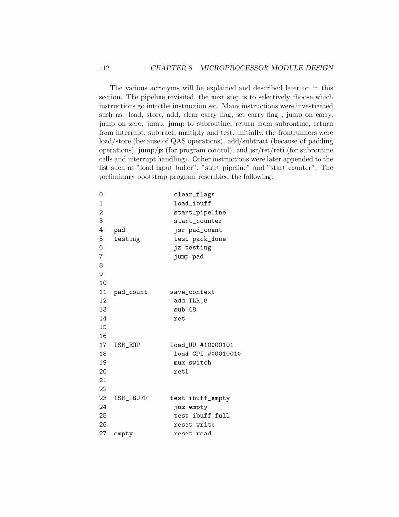
112 CHAPTER 8. MICROPROCESSOR MODULE DESIGN
The various acronyms will be explained and described later on in thissection. The pipeline revisited, the next step is to selectively choose whichinstructions go into the instruction set. Many instructions were investigatedsuch as: load, store, add, clear carry flag, set carry flag , jump on carry,jump on zero, jump, jump to subroutine, return from subroutine, returnfrom interrupt, subtract, multiply and test. Initially, the frontrunners wereload/store (because of QAS operations), add/subtract (because of paddingoperations), jump/jz (for program control), and jsr/ret/reti (for subroutinecalls and interrupt handling). Other instructions were later appended to thelist such as ”load input buffer”, ”start pipeline” and ”start counter”. Thepreliminary bootstrap program resembled the following:
0 clear_flags1 load_ibuff2 start_pipeline3 start_counter4 pad jsr pad_count5 testing test pack_done6 jz testing7 jump pad891011 pad_count save_context12 add TLR,813 sub 4814 ret151617 ISR_EOP load_UU #1000010118 load_CPI #0001001019 mux_switch20 reti212223 ISR_IBUFF test ibuff_empty24 jnz empty25 test ibuff_full26 reset write27 empty reset read

8.2. DESIGN HISTORY 113
28 reti293031 ISR_CRC move32 set pack_done33 reti
The previous program was written with the pipeline design already inmind. Thus, we start by clearing the ALU flags (such as the carry, zero,negative and pack done flags). Pack done will be used to indicate the com-pletion of the processing of a packet, and its subsequent placement intomemory. In short, the packet is ready for segmentation. The ”load ibuff”instruction was quickly annuled and joined with the ”start pipeline” instruc-tion. The latter commands the input buffer to open its gate and start feedingthe pipeline with packet bytes, one a clock cycle. The ”start counter” in-struction sends a control signal to the TLL to initiate the counting process.A jump to a subroutine follows, whereas the padding algorithm is imple-mented. First, the TLR (which contains the total length field, extractedfrom the IP packet) is added to the eight bytes that make up the trailer,and the latter value is decremented by 48 (the number of bytes to segmenteach cell to). Once the value reaches 0 or becomes negative, then we knowthat we have finished the padding algorithm, and the absolute value of thatnumber is the actual number of padding bytes. Please refer to the TLL sec-tion for a more in-depth discussion of the padding algorithm. The programabove does not completely implement the algorithm, because it was decidedthat the process should be implemented on the pipeline, and not be con-trolled through machine instructions. On the return of the subroutine call,we proceed to test for the Pack done signal. A unity value would indicatethat the ”ISR CRC” had executed and set the Pack done signal, otherwise,the ”CRC DONE” signal has yet to be asserted. The other two interruptsoccur when the TLL is done counting the packet, and when the input bufferis either empty or full. In either case, control signals have to be asserted,in order to control the bytes through the pipeline. An interesting featurein the ISR EOP (the TLL initiated ISR), is the fact that we can controlwhat the user would like to see in the UU and CPI fields of their IP packet.The vision was that these values would be read in from memory and storedinto special purpose registers within the microprocessor, and upon signaling,would be transferred over to the pipeline data bus, in order to complete thetrailer of the packet. This feature was scrapped due to the replacement ofthe interrupt mechanism by the main control unit.

114 CHAPTER 8. MICROPROCESSOR MODULE DESIGN
The initial microprocessor memory interface is shown in figure Initialmemory interface. The design involves the PC and the IR, but introducestwo new special purpose registers, mainly the stack pointer (SP) andthe address register (AR). The normal operation of the circuit involvesthe PC addressing a value in memory which is brought into the IR, andexecuted. The PC, meanwhile, gets incremented in order for it to pointto the next valid address of the program. The IR can provide the PCwith its value, instead of the incremented PC value, and that is becauseof the jump instruction, which causes the PC to be loaded with the jumpaddress with the latter stored within the jump instruction in the IR. Thereare a couple of variances to this scenario, and that is the additions of theinterrupt mechanism and the pipeline design. The interrupt mechanismrequires a register to point to an address in memory where the importantsystem information can be stored in the case of an interrupt occurring. Thisaddress is usually stored in the SP. The pipeline design, also introduces anew register. The reason for this is that the CRC module is required towrite out a byte of pipeline data every clock cycle. Hence, a mechanismmust be arranged in order to keep track of the address that the CRC writesto next. This address is stored in the AR. The external memory has an8-bit data bus, and a 12-bit address bus, thus, the total available memoryis 212 x 8 bytes, which comes out to 4,096 bytes or 4 kB. The memory itselfis byte-addressable, in that each address points to a byte of data.
Figure 8.4: Initial memory interface

8.2. DESIGN HISTORY 115
The initial memory map is shown in figure 8.5. It shows two majordecisions that were made. First, the largest IP packet that will be processedin the pipeline will be 100 bytes long, and the input buffer, in the worstcase, can only hold 10 maximum-sized IP packets. The memory is furthersubdivided into a QM and a PM, both of which are 10 kbytes long, and canhold 100 maximum-sized IP packets at any one time. The major differenceis that the PM holds them successively, in the order they appear, while theQM holds them in ordered queues (ordered according to priority). The lastsegment of the memory map is the program memory, which was chosen to be128 bytes long. The reasoning behind this is that all of the instructions are8 bits long, and thus in a jump instruction, the largest memory that we canjump to is 27 = 128 bytes away, assuming that the jump instruction itselfsteals the most significant bit of the instruction, and leaves us with 7 bits touse as an address to jump to (e.g. 10000111 decodes to a jump to memorylocation 3). The memory map was introduced in this section because of itsrelevancy to the microprocessor module. A more detailed description of thememory module can be found in the succeeding section.
Figure 8.5: Initial memory map
The instruction set was initially encoded according to table 8.1. Thistable shows that all instructions are 8 bits long, and that the largest mem-

116 CHAPTER 8. MICROPROCESSOR MODULE DESIGN
ory we can jump was changed to 32, because of the encoding of the jumpinstruction to to ”111a4a3a2a1a0”. Other significants are the operationsin the execute state of every instruction. Some instructions are typical,thus have common execution steps, but others, such as ”start counter” and”start pipeline” drive network functionality-specific control signals. Onelast point to mention about the instruction set is that during the fetch stateof all instructions, a byte of memory will be written out to memory, thusin register-transfer notation, the following would hold true ’RAM[AR] ←−CRC output’.
8.3 Functional Specification
The microprocessor chosen for implementation in this project, is an 8-bitmicroprocessor. All instruction opcodes are limited to 8 bits. The memoryis addressed with a 12-bit address bus, while the data path (according to ourpipeline structure) is 8 bits wide. The clock period was originally definedto be 40 ns, thus the clock frequency is 25 Mhz. This microprocessor fallsunder the RISC family of processors, as its instruction is quite reduced. Thefinal instruction set will be presented in this section. Also hardened will bethe memory interface, the bootstrap program, and the control units (yet tobe mentioned).
8.3.1 Instruction Set
The final instruction set was reduced to the following instructions: clear flags,start pipeline, start counter and jump. Their subsequent encoding is shownin table 8.2. Instead of explaining why all the other instructions were takenout, it is more valuable to mention why these particular instructions werekept in. The clear flags instruction allows us to, upon global reset of thesystem, to clear all the flags that might depict actions taken during the pre-vious operation. The start pipeline instruction allows us to signal the inputbuffer to start streaming the packet bytes. The start counter instructionallows us to inform the TLL (the first module on the pipeline) to commenceits starting sequence, in order to signal the ”End of Packet” state. Thefinal instruction, jump, is kept because it allows us to loop constantly uponpipeline initialization. Taken out of the design were the subroutine calls,the interrupt mechanism, the addition/subtraction control mechanisms, themux switch instruction and many more. The reasons vary from the use ofa piplined-design, to inherent operations executed within the pipeline (see

8.3. FUNCTIONAL SPECIFICATION 117
Mnemonic no. bytes Encoding Operationsclear flags 1 00000000 C ←− 0;N ←− 0; p d←− 0
start pipeline 1 00000010 TM rd←− 1start counter 1 00000011 TM start counting ←− 1;
test pack done 1 00000100 ifp d == 1 −→ Z = 1;elseZ = 0
test empty 1 00000101 ifempty == 1 −→ Z = 1;elseZ = 0
test full 1 00000110 iffull == 1 −→ Z = 1;elseZ = 0
add #h 1 0010h3h2h1h0 ACC ←− TLR + h;C ←− carry out
sub #l 1 01l5l4l3l2l1l0 ACC ←− ACC − l;C ←− carry out
jz #a 1 101a4a3a2a1a0 ifz == 1 −→ PC ←− a;elsePC ←− PC + 1
jsr #a 1 110a4a3a2a1a0 STACK[SP ]←− PC + 1;SP ←− SP + 1;
PC ←− a
jump #a 1 111a4a3a2a1a0 PC ←− a
ret 1 11111110 SP ←− SP − 1;PC ←− STACK[SP ]
reti 1 11111111 SP ←− SP − 1;ACC ←− STACK[SP ];
SP ←− SP − 1;PC ←− STACK[SP ]
Table 8.1: Instruction set encoding

118 CHAPTER 8. MICROPROCESSOR MODULE DESIGN
Mnemonic no. bytes Encoding Operationsclear flags 1 00000000 C ←− 0;N ←− 0; p d←− 0
start pipeline 1 00000010 TLL CU start←− 1start counter 1 00000011 tll startC ←− 1;
jump #a 1 111a4a3a2a1a0 PC ←− a
Table 8.2: Final instruction set
padding), to the desirable simplicity characteristic. The final bootstrap pro-gram follows:
0 clear_flags1 start_pipeline2 start_counter3 loop jump loop
The program is not very long, but does keep its major functionality:starting the pipeline. One of the many advantages of using a pipeline in ourdesign is shown here, as the bootstrap program (stored in ROM) does notneed to constantly control the pipeline. Some inherent control is done by thepipeline itself, along with the aid of a number of control units. The progamalso leaves room for future development by keeping the jump instruction.Not only does the instruction allow for branching to different parts of the 32bytes program memory, but it also performs a continuous loop in this case,and hence allows for easy interruption of the program, should the interruptmechanism deem useful at some time in the future.
8.3.2 Memory Interface
The final memory interface included a dissection of the previously designedinterface. As was shown in the final instruction set, the subroutine calls andthe interrupt mechanism are no longer needed, hence eliminating with themthe need for a stack pointer. One aspect that was modified from previousdesigns is the break up of the address registers into two: the write addressregister (WAR) and the read address register (RAR). The memoryitself will be discussed in the memory module design, but it is suffice tosay that the memory is a ternary-port memory. Traditionally, whenone needs to perform two operations upon the same memory, in one cycle,dual-port memory is utilized. In this project, we need to perform three

8.3. FUNCTIONAL SPECIFICATION 119
distinct operations upon the memory, all in one cycle. The operations arethe fetching of an instruction to be executed, the write out to memory abyte of packet information from the CRC module, and in some cases, theread out to the SAR module a byte of packet information from the memory.A solution to attempt to reduce the amount of ports on the memory (whichare a disadvantage, as each will require a data bus), is to multiplex at leasttwo of the addressing registers together, in order to alleviate the number ofdata buses to be interfaced to external memory, but this particular solutionwas not adopted because of two major reasons: first, the operations areindependent and do not have any relationships other than the RAR andWAR addressing the packet memory (queue memory was taken out becauseof the removal of the QAS module); the second reason for not adoptingmultiplexed addressing schemes is that a decision was made to design thememory internally, and thus avoid the external interface mechanism. Thedata buses are thus found within the chip, and do not cost the designers anymore than their routing specifications. The overall final memory interfaceis shown in figure 8.6. The PC is associated with the dual-port addressbus, while the IR is associated with the dual-port data bus. The mainaddress bus is connected to the WAR, while the value to write at the WAR’sdesignated address, is received from the CRC module. Finally, the RARis associated with the ternary-port address bus, while the SAR module isassociated with the ternary-port data bus. All data buses are 8 bits wide,while the address buses are 12 bits wide. That said, not all 12 bits are usedin address decoding, as will be seen later on.
At this point, we know who addresses what, but we don’t know how eachdoes it. There are three main addressing entities: the PC, the WAR and theRAR. Each is vital to the operation of the whole pipeline, with the WAR andRAR playing more eminent roles. The PC is designed according to tradition[dB98], but, as we can see, is not very important in the final design, as itdoes not address a very large program memory (32 bytes). The PC design isshown in figure 8.7. The operation of this register does not change from thedesign history section, except that it is worth noting the bus size limit of 5bits, as the PC only addresses (25) 32 bytes of program memory. The restof the address lines (DPA5-DPA11) are connected to the power supply tocause the program memory to be addressed to the end part of the memory(see figure ??). The WAR and RAR operate according to figures 8.8 and 8.9.They address the memories for the CRC module to write to, and for the SARmodule to read from. The actual transfer of the data is co-ordinated by theaddress control unit (discussed below). The WAR differs from the RAR,in that the former increments normally, until the jump war control signal

120 CHAPTER 8. MICROPROCESSOR MODULE DESIGN
Figure 8.6: Final memory interface
is asserted, whence a switch is made to accept the pad register (PR) valueinto the adder circuitry. This will perform the padding algorithm, in that,upon command, a certain amount of memory locations will be effectivelyskipped, and since the packet memory is initialized with zeroes, a certainamount of pad bytes will be inherently appended to the packet. This willwork as long as zeroes are re-written into the memory location just read outto the SAR module. Conversely, the RAR only has to increment after eachread (and its trigger to start reading), in order to address the bytes of thepacket to be read out next. The control signals designated in the previousthree diagrams will be discussed in the control units section below.
Figure 8.7: PC architecture

8.3. FUNCTIONAL SPECIFICATION 121
Figure 8.8: WAR architecture
Figure 8.9: RAR architecture
8.3.3 Control Units
Proknet contains a microprocessor which performs all of the previously men-tioned tasks. However, the CPU is partitioned into three main units: theinstruction control unit (ICU), the address control unit (ACU) andthe main control unit (MCU). The instruction control unit is the leastcomplex of all three, and will be the first presented.
ICU design
The ICU was partially modified from the original state machine to look likefigure 8.10. The assertion of global reset causes the finite state machine(FSM) to enter its reset state, where all the machine’s outputs are reset.The PC is loaded with its initial value, and the inc pc signal is asserted to in-dicate the increment of the PC after fetching the first instruction. The Fetchstate loads the IR (by assertion of load ir) with the data from the memory(the actual instruction to be decoded), and the Decode and Execute stateactually performs the decoding and the execution, as all four instructionsdo not require more than one clock cycle (no operands to fetch) to execute.Depending on the received instruction, certain control signals are asserted,and then de-asserted. The instructions are all stored in ROM, and henceare fetched on start up. At this moment, it is worth mentioning that theinstructions and the instruction control unit do not add or hinder the overallprocess. The functionality that was supposed to be an advantage was mostly

122 CHAPTER 8. MICROPROCESSOR MODULE DESIGN
replaced by the introduction of the other two control units, and hence thisunit has nearly become obsolete. It is however interesting to note that thisunit is functioning, and if need be, can be utilized in future releases. Theonly utilized function is the TLL CU startC signal, which is the ICU’s sig-nal to the TLL to commence counting (for the very first time). The latteris asserted upon decoding of the start counter instruction.
Figure 8.10: ICU FSM
ACU design
The ACU is a more vital control unit, and its corresponding FSM is shown infigure 8.11. As we can see from the figure, the assertion of the global resetputs us directly in the Reset state. The assertion of the TLL CU startCsignal from the ICU, will trigger a move to the CRC start state, where theWAR begins to increment (from zero), in order to address valid locations towrite bytes out to (assertion of load war and inc war control signals). TheFSM transitions to the Idle state on the next clock edge (remember that allour FSMs are sequentially designed around our 25 Mhz clock). The FSMremains in the Idle state unless one of the following occurs:
1 The TLL module finished counting the number of bytes in the packet(assertion of TLL eop)
• The jump war signal is asserted to execute a jump according theamount of padding bytes we have to append;
2 The CRC module finishes writing a packet out to memory (assertionCRC eop)

8.3. FUNCTIONAL SPECIFICATION 123
• The load rar and inc rar signals are asserted to load the RAR andallowing it to start incrementing to feed the SAR module withits bytes of packet information (the oe tp signal is also assertedto allow ternary-port reads, while the we signal is de-asserted todisallow writes from the CRC module to the packet memory);
3 The SAR module completes the segmentation of a packet (assertion ofSAR pd)
• The inc rar and oe tp signals are de-asserted to disallow readsfrom the ternary-port memory;
4 A new packet comes into the pipeline (assertion of stimulus startC)
• The we and inc war signals are re-asserted to allow writes fromthe CRC module again.
As a side note, upon reset none of the control signals are asserted. Also,the CRC restart state was added in order to allow the pipeline to handlemore than one packet simultaneously. Finally, all secondary states (the onesfollowing the Idle state) are transitions states, in that they transition backto the Idle state after one clock cycle.
Figure 8.11: ACU FSM

124 CHAPTER 8. MICROPROCESSOR MODULE DESIGN
MCU design
The MCU is the nucleus of Proknet. Its corresponding FSM is shown infigure 8.12. Instead of attempting to explain the packed FSM, it would beeasier to outline the main functions of the MCU:
1- TLL
• Start the TLL counter through the assertion of TLL startC ;
• Handle the TLL eop signal indicating the end of the packet.
2- Trailer
• Drive read and write signals to the trailer FIFO buffer;
• Drive a form of TLL eop to the trailer called CU T eop;
• Drive a T clr cntr signal to clear the trailer counter;
• Handle T eop signal indicating the end of the trailing for the packet;
• Handle Empty and Full signals indicating the status of the FIFObuffer.
3- CRC
• Drive read and write signals to the CRC FIFO buffer;
• Drive a form of T eop to the CRC called CU CRC eop;
• Handle CRC eop signal indicating the end of the write to memory ofthe packet;
• Handle Empty and Full signals indicating the status of the FIFObuffer.
4- SAR
• Drive SAR startC upon reception of CRC eop;
• Drive Start Address and End Address which indicate the start andend of the packet in memory;
• Handle SAR pd signal indicating the completion of the segmentationprocess for one packet.

8.4. HARDWARE SPECIFICATION 125
The MCU operates on global reset as well, whereas it resets all of itscorresponding output signals. The control unit is also provisioned to handlemultiple packets on the pipeline as indicated in the FSM. The transitionstates were carefully selected, after numerous sample scenario runs. Forexample, a T eop transition can only occur when the machine is in its TLLor Trailer states, because otherwise the trailer has already been completed,and hence, the T eop signal has already been asserted and de-asserted.
8.4 Hardware Specification
The microprocessor module is implemented using the Verilog [DET95][Smi96]language. Its main components are as described above in the FunctionalSpecification section. The source code can be revised by looking at AppendixD (or in directory /proknet/ucpu, on the accompanying CD). There arethree main files: ’inst cntrl unit.v’, ’address control unit.v’ and ’main control unit.v’.The microprocessor functionalities (PC, IR) are implemented in the ICUdesign, while the network-processor functionalities (WAR, RAR) are imple-mented in the ACU. The MCU controls the pipeline, and hence has manyother functionalities. All three files contain standard Verilog state machines,with one caveat. The MCU contains a ”previous state” registered value,which aids in the implementation of the FSM. This is necessary because ofdifferent transitions within the state machine, hence we need a certain signalto keep reminding us where the previous state, and hence, how we got to bein the present state.
The implementation scheme for this module was chosen to be the be-havioural one. Although most of the project was implemented in RTL-stylecode, it would have been fruitless to attempt to do the same to this mod-ule, as this module contained entities that were better-suited for a statemachine type of design, and hence, the behavioural representation in Ver-ilog. The registers (PC, IR, WAR and RAR) were also implemented be-haviourally (using always @ blocks) to follow with the top level structure ofthis module. Other notables are the fact that addition was also implementedbehaviourally. We had at our disposal a fully functional ALU, capable ofadding/subtracting two 16 bit numbers, but it was tightly controlled by thepipeline itself, and hence could not have its control shifted towards the MCUwithout paying a price.

126 CHAPTER 8. MICROPROCESSOR MODULE DESIGN
Figure 8.12: MCU FSM
8.5 Functional Simulation
Functional simulation was run on the microprocessor top level module, andthe corresponding results are shown in figure ??. Functional simulation ofthis module included the instantiation of the memory module. Now, al-though the latter has not been formally introduced (following), it has beendiscussed enough to appreciate its projected objectives. The top level mod-ule of the microprocessor is termed ucpu top, while the test bench module istermed tb ucpu. The former is instantiated in the latter, and subsequentlytested by the variation of the inputs to the module. As we can see fromthe functional simulation, the MCU starts out in the Reset state (state 0),and upon reception of a start again signal indicating a new packet to be

8.6. SYNTHESIS 127
processed, proceeds to the Idle (state 1) and then the TLL (state 2) stateright after. In between, a tll startC signal is sent to the TLL module in-structing to commence the counting process. The trailer and CRC moduleread and write signals also are driven. They actually have the same charac-teristics as the system clock, since we need to write and read bytes to eachof the trailer and CRC module FIFO buffers every clock cycle, in order tofulfill our pipline requirements. The MCU remains in the TLL state untilit receives feedback from the module that it has completed the countingprocess (tll eop), upon which the MCU transitions to the Trailer (state 3)state, and sends the trailer module a signal (cu to trailer eop) to indicateTLL completion, and TLR and PR validity. The machine remains in theTrailer state until it receives feedback from the module that it has com-pleted the trailing process (t eop), upon which the MCU transitions to theCRC (state 4) state, sends the CRC module a signal (cu to crc eop) to indi-cate trailer completion, and clears the trailer module’s counter by assertingclear trailer counter. The MCU remains in the CRC state until it receivesfeedback from the module that is has completed the processing of the packet,which is safely stored in packet memory, through the assertion of crc eop.The MCU then transitions to the SAR (state 5), and subsequently to theSAR waiting (state 6) state, clears the CRC FIFO buffer by resetting bothpointers (clear read ptr and clear write ptr), and sends a signal to the SARmodule (sar startC) indicating to it that there is a packet in memory readyfor segmentation. The SAR proceeds in the segmentation process, and uponcompletion, signals the MCU with the assertion of sar pd (sar packetdone),whence the MCU transitions back to the Idle state awaiting a new packetto come into the pipeline (signaled by start again).
8.6 Synthesis
The microprocessor module was synthesized using ”Design Analyzer” pro-vided by Cadence. This software allows the designer to input Verilog sourcefiles, and generates schematics for each of the modules utilized within thedesign. Referring to appendix D, we can see the synthesis outputs for all themodules in the microprocessor module. By looking at the top level module,ucpu top, we can see the symbol and schematic diagrams that represent andimplement the module, respectively. The symbol diagram presents us witha black-box view of the module, only showing the inputs and outputs of themodule, as well as the width of each input or output. The schematic diagramon the other hand presents us with the underlying structure (a white-box

128 CHAPTER 8. MICROPROCESSOR MODULE DESIGN
view) of the module. First, we can see that the module contains four othermodule instantiations, which is according to specification. The four inter-nal modules are: instr cntrl unit, address cntrl unit, main cntrl unit andtp ram memory. The former three will be discussed below, but the latterwill be left for the synthesis discussion of the memory module.
The three FSMs discussed earlier control the entire system. The Ver-ilog source code was written behaviourally, and for that matter, it is notsimple to recognize the output of the synthesis process. That said, therea few components that should be easily spotted, including all of the stateflip-flops, and the output construction logic. For example, looking at themain cntrl unit schematic, we can trace the crc read signal output and howit was generated. It is the output of an 2-input AND gate. One of the inputsis the global system clock, while the other is the output of an internal latch.The latch has an internal logic generated input, but also has an enable tiedto it. The enable is used to disable reading from the CRC FIFO buffer. Thisis again according to specification.
8.7 Timing Simulation
This section is yet to be completed. The issue here is that the microprocessormodule instantiates the memory module. That said, the latter was writtenin a brute-force behavioural fashion, and thus has caused the synthesis toolto halt because of a lack of host machine memory. The memory module isquite a large design, including 64 kB of RAM cell components. Includedin the memory module are various address decoder instantiations, which donot help the size of the module. The synthesis tool handles the reading ofall Verilog source files, and a first-attempt compilation. The synthesis toolorders the designer to ”uniquify” all multiply-declared instantiations. Uponthe completion of that request, the designer attempts a final compilationstep, whereas the synthesis tools utilizes around 1.18 GB of memory, butstill manages to crash. This issue is a major one, as the designer needsto revert back to the design of the memory, and investigate other optionsto create the memory. A simple solution would be to interface to externalmemory, which would actually be the ideal situation. The reason for notperforming that in the first place, is that it was thought easier to create amemory that is less than 5 kB in size within the design itself.

Chapter 9
Memory Module Design
9.1 Theory
The last topic of discussion is the memory module design. Memory is a largearray of storage cells, each capable of holding one bit of information [Kli82].Traditionally, the CPU accesses the memory by altering a number of bits at atime, and thus memory is usually byte addressable. The number of bits thatcould be altered at any one time is termed the width of the memory, whichchanges from computer to computer. An address is associated with each byteof memory, because the latter is not usually accessed in a linear fashion, andthus requires a mechanism of control. The number of addressable bytes inthe address space will be a power of 2, calculated by taking the power of2 to the number of address lines present on the address bus. For example,for a 16 bit address bus, there are 216, or 65,536 different memory locationsthat could be written to or read from. The size of the memory is usuallydescribed by two numbers: the number of total different memory locationsand the width of the memory. Thus, typical values for memory sizes include2kB x 8 or 16kB x 4 (the unit kB equaling 1024 bytes).
Normal memory is designed with one write enable line and one outputenable line, in order to be able to read or write to memory. There is anothertype of memory that allows for the reading and writing out to memory at thesame time called dual-port memory. If on the other hand, two writes wereto occur at the same time, some extra logic would have to be built in orderto make sure that both writes do not occur on the same memory location.The write enable line is a single wire driven by the microprocessor to controlthe function of the memory. If the write enable control line is asserted asa logical one, i.e., ”true”, then the memory performs a write operation. If
129

130 CHAPTER 9. MEMORY MODULE DESIGN
it is asserted as a logic zero, i.e., ”false” then the memory cannot write outto memory. The same logic holds for the output enable line, only that itcontrols read operations.
The system memory is usually described by a memory map, which servesto section off the different types of memory. The read/write memory, theread-only memory, and the write-once memory (if present) have to be delin-eated in terms of address space, in order to correctly address them internallyin the microprocessor’s memory interface. Traditionally, it is advantageousto place the program space at the opposite end of the memory compared tothe data or user space. An address decoding mechanism also has to be putinto place in order to easily address a memory location by not having to de-code all the address lines on the bus. It is worth noting that a chip select(CS) signal is usually used when multiple devices are interfaced to the mi-croprocessor, but in this scenario only the memory is interfaced, requiringone CS signal. Delving further, the designed memory is not external, andhence will actually not even require a CS signal to interface to, however,does require a write enable and output enable(s) in order to correctly readand write to memory locations.
There are numerous types of memories: asynchronous, synchronous,dual-port, first-in-first-out. A brief discussion of each follows. Asynchronousmemory allows for new data to be written to it just by changing the addresslines, and hence the write enable lines. For this characteristic, a majorrestriction is put into effect, and that is that the new address line mustremain stable for a certain period of time before the actual write enableline changes. Synchronous memory on the other hand, handles these typesof situations much more efficiently, as it is quite easier to analyze signalchanges for setup and hold-time violations. All signals are synchronized toa global clock, thus are easier to analyze. Dual-port memory has alreadybeen discussed. Finally, first-in-first-out (FIFO) buffer memory is used toaccept short bursts of high-speed data from the input side, and output themto the receiver at a rate that the latter can handle. FIFO buffers are mostlyutilized in communication systems, and have already been discussed in thetrailer and CRC module design sections [dB98].
9.2 Design History
The memory was one of the last modules to be designed and implemented.For this matter, it was already outlined in terms of functionality, inputs andoutputs as presented in the microprocessor module design section. As can

9.2. DESIGN HISTORY 131
be seen in figure 8.5, the input buffer was thought to be contained withinthe system memory. A buffer control unit would be controlled by the MCU,and thus the pipeline would be fed with the bytes of the packets accord-ingly. The initial design for the memory was for a single-port synchronousmemory, as shown in figure Initial memory interface. The design includedone input/output bus that would allow for read operations (into the IR),and write operations (from the CRC module). This solution quickly be-came disbanded for many reasons. First, as mentioned before, we will needto perform three different operations simultaneously. One issue to mentionis that we will not have to introduce any external circuitry to disallow twowrites to the same memory location, because the three operations are onewrite, and two read operations (Two reads to the same memory locationare allowed). For this matter, the implemented memory is a ternary-portmemory (TPRAM). It is, as mentioned, synchronized to the global 25Mhz clock, and hence, the memory location values can only be altered atthe edge of the global clock, and not at the edge of the write enable lines(as in asynchronous memories).
The memory itself is a 4kB large, and its size is represented by thefollowing notation: 4kB x 8, meaning that there are 4,096 total addressablememory locations with a memory width of 8 bits. The total valid memorylocations came about by taking the power of 2 to the number of addresslines, the latter being 12. Thus, 212 equates to 4,096 memory locations.The address bus width was chosen to be 12 bits, because packet memory isdefined to be 1 kB large, and the program space is defined to be 32 byteslong. Hence, for further expansion, a sensible amount of unused memorywas placed in, and thus the 12 bit addressing scheme was selected. Thememory has one write enable line (w en) to allow for the writes from theCRC module, and two output enable lines, one to enable reads to the SARmodule (tp rd), and the other to enable reads to the IR (dp rd). Each ofthese signals are actually buses that should be 4,096 bits wide, but becauseof address decoding are less than that. This point will be delved into in thenext section.
The need memory being only a few kilobytes large, it was unnecessaryto interface to external memory, and thus it was chosen to implement thememory internally. That said, an initial design of a RAM cell is shown infigure 9.1. This RAM cell is only used to instantiate two of the ports of theTPRAM. The third port is actually the dual-port which feeds the IR, and ispresented in the ROM design section. The RAM cell will be the basis used tomake all of the system memory, and will hold all of the packet information.It will be the lowest entity that will be visible in terms of system memory.

132 CHAPTER 9. MEMORY MODULE DESIGN
An address decoding mechanism will have to be used to address the differenttypes of memory, but its discussion will also be left for the next section, asno major design iterations were spent on it.
Figure 9.1: RAM cell
9.3 Functional Specification
The new memory map is shown in figure 9.2. The only addressable spacesare the packet memory and program spaces. The program space is actu-ally a 32 byte ROM implementation, while the packet memory is a 1 kBRAM implementation. The latter, as previously mentioned, took its shapefrom the basic RAM cell. From the small building blocks (RAM cells), awhole memory system was generated. More on this topic in the hardwarespecification that follows.
Another major block of the memory module is the address decodingscheme. There were two major types: the microprocessor address decodingscheme, and the network processor address decoding scheme. The former isillustrated in figure 9.3. It can be shown that from the address DPA5-DPA0,and the oe dp enable line, the 32 output enable lines can be generated, soas to read the correct memory location. The network processor addressdecoding scheme is much more complex and will not be shown here, as it isjust an extension of the ideologies presented in the MCPU address decodingscheme.

9.4. HARDWARE SPECIFICATION 133
Figure 9.2: Final memory map
One last point is the input buffer implementation. It was decided, thatsince the input buffer usually feeds the IP over ATM segmenter, it wouldbe logical for it to be the output of a buffer or another chip sitting on theboard. That said, it would be quite unrealistic to store the buffer in themain memory as depicted in the initial memory map. or this reason, theinput buffer will be moved from the main memory, and into the final testbench of the top level module. A brief period of time was spent in orderto attempt to place the input buffer into a file, which could be read intothe Verilog simulation environment, but was not implemented due to timeconstraints.
9.4 Hardware Specification
In order to generate the system memory, eight RAM cells were instantiatedto make a byte, then eight bytes were instantiated to make 8 bytes, eight ofwhich were instantiated to make 64 bytes, eight of which were instantiatedto make 512 bytes. Now, the memory space was modified during the addressdecoding, since the WAR and RAR only used the least significant 10 bitsto address their common space, the packet memory, while the PC only usedthe least significant 5 bits to address its space, the program space. The PCwas picked as the dual port, while the WAR was the single port, and the

134 CHAPTER 9. MEMORY MODULE DESIGN
Figure 9.3: Micro-CPU address decoding
RAR was the ternary port. That said, we come to an earlier point thatthere less than 4,096 w en/dp rd/tp rd lines. This holds true because of theaddress decoding simplifications. There are only 32 dp rd lines, as there areonly 32 bytes of ROM to read from, while there are 1,024 w en/tp rd linesto encompas the 1 kB of packet memory. One major design change is thereduction of the address space to 2 kB, as indicated by the 10 bit addressdecoding of the WAR and RAR. That said, to instantiate 2 kB of memory(32 bytes of which is ROM, and the rest RAM), we included three 512 byteRAM instantiations, seven 64 byte RAM instantiations, one 32 byte RAMinstantiation, and of course, one 32 byte ROM instantiation (3*512 + 7*64+ 2*32 = 2,048).
The ROM block was written in behavioural code. Its mode of operationis quite simple: when queried with an address, decode it and drive the correctdp rd line, whereas the data bus connected to the IR, will be filled with theROM byte at that memory location (see accompanying source code, or CD

9.5. FUNCTIONAL SIMULATION 135
directory /proknet/memory/rom 32bytes.v).The address decoding block was implemented according to the truth ta-
ble implementations of each decoder. There are three decoder blocks: thetwo-to-four decoder, the three-to-eight decoder and the four-to-sixteen de-coder. All three are utilized in the decoding scheme, and their instantiationsand interconnections can be seen by looking at the source code (see accompa-nying source code, or CD directory /proknet/memory/address decoder.v).
9.5 Functional Simulation
Functional simulation was run on the memory top level module, and thecorresponding results are shown in figure Memory functional simulation.The top level module of the memory is termed tp ram memory, while thetest bench module is termed tb memory. The former is instantiated inthe latter, and subsequently tested by the variation of the inputs to themodule. As we can see from the functional simulation, the outputs matchour desired results. Upon global reset, our ROM begins to output bytesof data to the IR, whence the oe dp output enable line to the dual port isenabled. The ROM will output one instruction to the IR every clock cycle.These instructions were initialized in the ROM source file. We can also seethat the PC is incrementing every clock cycle to address the next memorylocation. Another observation to make is that the CRC module writes twobytes out to memory, the first with a value of 0x12 to address 0x008, whilethe second is 0x0F to address 0x004. The write en signal is asserted eachtime a write is initiated. On the other side, the oe tp output enable signalis asserted once the SAR module is ready for its data, which happens to be0x12 and 0x0F, stored at addresses 0x008 and 0x004, consecutively. Thisdemonstrates the correct functionality of the TPRAM.
9.6 Synthesis
The memory module was synthesized using ”Design Analyzer” provided byCadence. This software allows the designer to input Verilog source files,and generates schematics for each of the modules utilized within the design.Referring to appendix E, we can see the synthesis outputs for all the modulesin the memory module. By looking at the top level module, tp ram memory,we can see the symbol and schematic diagrams that represent and implementthe module, respectively. The symbol diagram presents us with a black-box

136 CHAPTER 9. MEMORY MODULE DESIGN
view of the module, only showing the inputs and outputs of the module, aswell as the width of each input or output. The schematic diagram on theother hand presents us with the underlying structure (a white-box view) ofthe module. First, we can see that the module contains two other moduleinstantiations, which is according to specification. The two internal modulesare: address decoder and ram 2kbytez.
The address decoder module contains numerous instantiations of thethree main address decoding modules: two four decoder, three eight decoderand four sixteen decoder. Please refer to section 9.2 for a more detailed dis-cussion of the design history of this module. The interesting note to observewhen referring to the address decoding synthesis outputs is that only NOTand AND gates are utilized to implement the modules. This was expected asthe modules’ Verilog code only mapped out the truth table of each decoderinto source code. The truth tables are easily implemented using NOT andAND gates, which was actually the truth.
The ram 2kbytez module contains numerous instantiations of the smallermemory modules: ram 512bytez, ram 64bytez, ram 32bytez, ram 8bytez,ram byte z, ram cellz and rom 32bytez. The basic module is the ram cellz,which is implemented using a flip-flop and other combinational logic. Themain specifications of the memory can be reviewed in section 9.3.
9.7 Timing Simulation
Please refer to section 8.7 for a discussion of this task.

Part IV
Conclusions
137


Chapter 10
System Integration
10.1 Proknet c©in all its might
10.1.1 System Integration
This part of the project was divided into three parts:
• TLL and Trailer Integration. (see Appendix G, tll trailer top.v)
• TLL, Trailer and CRC integration. (see Appendix G, tll trailer crc top.v)
• TLL, Trailer, CRC, SAR and Micro CPU and Memory integrationwhich is know as Proknet. (see Appendix G, final top.v)
The reason for this is to assure that the modules are carefully studiedand that their behaviors well understood; that way it becomes easier todebug as the integration progresses.
10.1.2 Functional and Hardware Specification
As far as functional and hardware specifications go, nothing was changedin the designed modules of the pipeline. In each integration phase, theappropriate modules were instantiated, and valid inputs and outputs werepassed as was designed in the pipeline.
10.1.3 Functional Simulation
For TLL and trailer integration, a test bench (see Appendix G, tll trailer top tb.v)was written in order to model the control unit’s actions (see Appendix G),
139

140 CHAPTER 10. SYSTEM INTEGRATION
and to test their functionality together (see Appendix G for timing dia-grams). In the first timing diagram (Tll Trailer Integration(1/2)), a packetwas received on the pipeline(In data bus) and StartC (start counting) wasasserted to allow the TLL module to extract the length of the packet andto compute the padding bytes. As shown, the bytes of the packet were putout to the pipeline (out data bus), a clock cycle later from when it was re-ceived. This cycle keeps going until the TLL module sets the eop signalhigh, which causes the control unit to set cu eop high for 8 clock cycles,which allows the trailer module to output the trailer fields (see AppendixG, Tll Trailer Integration (2/2)).
Knowing that the TLL and trailer modules functioned properly, the CRCmodule was merged and integrated along with (see Appendix G, tll trailer crc.v).A test bench was written to test the functionality of all three modules (seeAppendix G, tll trailer crc top tb.v). The main concern in this part was tosee if the CRC module will output the 4 bytes of CRC at the given signalcu c eop (it is set by the control unit when signal doneT is received fromthe trailer module), this signal will stay high for 4 clock cycles.
Having done so many integrations and feeling very comfortable with theoutputs and timing diagrams, it was time to pick up the speed and merge therest of the modules (SAR, MicroCPU and Memory). Please refer to ProknetTop Level Functional Simulation 1,2 and 3 as the discussion progresses. Apacket of 16 bytes was put on the pipeline and the signal start again isasserted to indicate the arrival of a new packet. The packet goes throughthe TLL module and the following occurs:
• Extractor extracted the TL (total length of the packet) and stored inTLR (16).
• Pad Unit computed the number of pad bits needed and displayed byPR (24).
• Packet kept flowing through the TLL, trailer (because CU T eop islow), CRC (because CU CRC EOP is low) until the TLL eop signalis set high.
Just a reminder that 16 (length of packet) + 24 (output of pad algorithm)bytes of padding + 8 bytes of Trailer = 48 bytes. Therefore the packet isdivisible by 48.
When TLL eop was set high by the TLL module, the Control Unit setCU T eop high for eight clock cycles in the Trailer Module which in return:
10.2. PROKNET c©LIMITATIONS 141
• Switches the 2 to 1 mux and triggers the 3-bit counter to start count-ing;
• The 3-bit counter is the selector of the 8 bytes trailer, therefore as itcounts, it is outputting the trailer fields to the pipeline. When the3-bit counter is done counting, it sends a T eop back to the MCU.
When T eop is received by the MCU, CU CRC EOP is asserted for fourclock cycles which causes the following to occur in the CRC module:
• Switches the 2 to 1 mux and triggers the 2-bit counter to start count-ing;
• The 2-bit counter is the selector to the 4 bytes of valid CRC thatwere computed by the CRC-32 unit, so as the 2-bit counter counts,it is selecting the CRC bytes and putting them out onto the pipeline.(Please see crc data out, notice the Trailer and CRC). When the 2-bitCounter is done counting it sends CRC eop (it means CRC has beenappended) to the MCU.
Upon receiving the CRC eop, the main control unit sends a SAR startCsignal to the SAR module, which causes the following to occur:
• Counter is triggered (see atmcounter), and the counter keeps countingup to 48 then;
• Cell Done is asserted, meaning that 1 48 byte cell has been sent.
• Packet done goes high which means that 1 IP packet has been pro-cessed.
10.1.4 Synthesis
Synthesis was previously separately done on each module (please refer tothe individual modules for more information).
10.2 Proknet c©limitations
The following section is brief liaison of all the major hurdles that have beenleft behind because of a major lack of resources, be it time, man-power ordevelopment tools. The major task to be handled is the completion of thepadding algorithm. The latter requires a module to write back zeroes into

142 CHAPTER 10. SYSTEM INTEGRATION
the just-read bytes of memory. The original thought was that the SARwould accomplish this task, but it turned out too memory intensive, as arecord of the start and end addresses of the previous packet have to be kept.The other module that could have taken care of this is the micro-processormodule, but the latter already was interfaced to a TPRAM, and was notable to handle more ports, or multiplex the data on one of the existing ports.
A major limitation of Proknet is that it cannot handle more than 2packets on the pipeline. It can on the other hand handle 1 packet (the sizebeing smaller or greater than 48 bytes), and 2 packets. The limitation isthat when more than 2 packets are present on the pipeline, the TLR andPR registers, as well as the Start Address and End Address lines all latchor store values of the next packet, while the previous one is being processedby the SAR module.
An ATM specification change was made during the design, and that is toonly perform the byte-wise CRC calculations on the packet and the trailer,excluding the padding bytes. The reason for that is simplicity of design.In order to make up for this specification change, an assumption about thereassembly side was made: the reassembler will strip the padding bytes first,and then calculate its own CRC to see if it matches the packet’s sent CRCinformation (4 bytes of it).
As previously mentioned, a queuing and scheduling module was supposedto add extra functionality to Proknet, but it was scrapped as soon as thepriorities were handed down by the members of the group. Queuing andscheduling was seen as a luxury to have, rather than a necessity for thecorrect operation of the system.
As aforementioned as well, the timing simulation phase of the projectdid not succeed as anticipated. Numerous problems were faced from designmethodologies, to library problems to memory constraints. Please see eachmodule design section for more detail on this topic.
Finally, by looking at the final top level functional simulation, we cansee that there are two bytes that are not propagated to the output of thepipeline. The reason for that is found in a design error. The FIFO bufferswere designed to hold exactly the same amount of bytes as each module(trailer and CRC) was transmitting. For this reason, the buffer would getfull, and then would have to be emptied by one byte first, before allowing awrite operation on the buffer. For this reason, a byte is lost in each buffer,and is not saved, but actually overwritten in the buffer. A resolution to thisproblem would be to increase each buffer’s size by one, making the trailerFIFO buffer a 9-byte buffer, and the CRC FIFO buffer a 5-byte buffer.

10.3. FUTURE WORK 143
10.3 Future Work
Proknet has managed to successfully segment variable-sized IP packets intofixed-sized ATM cells. That basic functionality was implemented and func-tioned correctly. What is missing are all the extra caveats that were thoughtup in the preliminary design phase of the project. Queuing and scheduling isa great luxury to have, and would have to be the first module implementedif Proknet 1.0 were to come out. Other major improvements would bea greater pipeline throughput, a correct (according to specification) CRCcalculation, and a correct implementation of the padding algorithm. Re-viewing the current limitations of Proknet, it would be a great improvementto successfully simulate the timing characteristics, and place and route thedesign. Proknet would then become an entity ready to be implemented onany programmable chip.
Proknet could also benefit from a parallel architecture, where multiplepipelines could be executing on various packets. This system would have tobe a massively-parallel system, but would increase the throughput by leapsand bounds. This idea could be beneficial in the re-engineering of today’sSARs on the market, as they operate on a queuing and scheduling algorithm,but do not include multiple pipelines.
10.4 Project Conclusions
This project started off as a migration from traditional microprocessor de-sign to a more innovative network processor design. The idea was a raw one,with only a few references to go by. The design work accomplished provedthat this technology is of great benefit to the networking world. Today’smajor (communication) industry players use SARs as commonly as they useresistors on their printed circuit boards. Proknet was born in a small designroom in McDonald Hall at the University of Ottawa, but its birth gave truedesign experience to its parents. It has also come a long way from the blockdiagrams that were ”supposed” to segment a packet into smaller chunks,and has flourished into a working Verilog model, as well as a synthesizednetlist.
To make the really long story long, the project’s main objectives havebeen met. The designers believe that they have acquired a great deal ofknowledge by doing everyday designer tasks. One point to be stressed is thefact that the implementation phase should have been guarded against, asthe designers did spend quite a long time in the design phase. As a result

144 CHAPTER 10. SYSTEM INTEGRATION
though, a straightforward implementation eased the flow into synthesis.Proknet is alive and well. It is awaiting its total completion, but stands
before you today, as a valid IP over ATM segmentation entity.

Bibliography
[1.697] Wordnet 1.6. Org from ftp://clarity.princeton.edu/pub/wordnet/wn1.6unix.tar.gz.Technical report, Princeton University, 1997.
[Cle92] Alan Clements. Microprocessor Systems Design: 68000 Hardware,Software, and Interfacing. PWS Publishing Company, 20 ParkPlaza, Boston, Massachusetts 02116, 2nd edition, 1992.
[dB98] Dave Van den Bout. The practical Xilinx Designer Lab Book.Xilinx Inc., 1998.
[DET95] Philip R. Moorby David E. Thomas. The Verilog Hardware De-scription Language. Kluwer Academic Publishers, Reading, Mas-sachussetts, 1995.
[Hal92] Fred Halasall. Data Communications, Computer Networks andOpen Systems. Addison-Wesley Publishers Limited, 1992.
[Ibe97] Oliver C. Ibe. Essentials of ATM Networks and Services. AddisonWesley Longman Inc., 1997.
[Kli82] Edwin E. Klingman. Microprocessor Systems Design, Microcoding,Array Logic, and Architectural Design. Prentice Hall Inc., 1982.
[Lee00] Sunggu Lee. Design of Computers and Other Complex DigitalDevices. Prentice Hall, 2000.
[Pry95] Martin De Prycker. Asynchronous Transfer Mode Solution forBroadband ISDN. Prentice Hall International (UK) Limited, 1995.
[Smi96] Douglas J. Smith. HDL Chip Design. Doone Publications, 1996.
[Tan96] Andrew S. Tanenbaum. Computer Networks. Prentice Hall PTR,1996.
145

146 BIBLIOGRAPHY
[Tre87] Nick Tredennick. Microprocessor Logic Design. Digital EquipmentCorporation, 1987.

Appendix A
A - TLL module
147

148 APPENDIX A. A - TLL MODULE

Appendix B
B - Trailer module
149

150 APPENDIX B. B - TRAILER MODULE

Appendix C
C - CRC module
151

152 APPENDIX C. C - CRC MODULE

Appendix D
D - Microprocessor module
153

154 APPENDIX D. D - MICROPROCESSOR MODULE

Appendix E
E - Memory module
155

156 APPENDIX E. E - MEMORY MODULE

Appendix F
F - SAR module
157

158 APPENDIX F. F - SAR MODULE

Appendix G
G - System Integration
159

160 APPENDIX G. G - SYSTEM INTEGRATION

Appendix H
H - Design Documents
161

162 APPENDIX H. H - DESIGN DOCUMENTS

Appendix I
I - Project Presentation
163