programmable logic devices and architectures · programmable logic devices and architectures ......
TRANSCRIPT
Programmable Logic Devices and Architectures
R.Roosta

What We Will Cover
• programmable logic types• Device architectures• Device performance• Packaging• Reliability• Radiation considerations• Lessons learned
Applications
• Existing SSI/MSI Integration• Obsolete/"Non-Space-Qualified" Component
Replacement• Bus Controllers/Interfaces• Memory Controller/Scrubber• High-Performance DSP• Processors• Systems on a Chip (SOC)• Other Digital Circuits

SSI/MSI Logic Integration
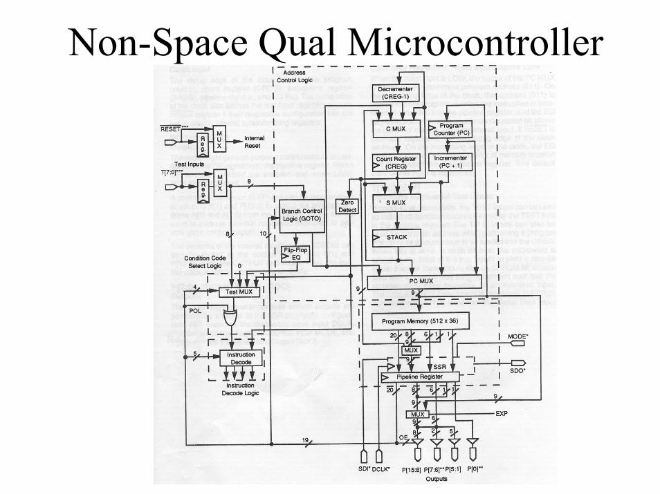
Non-Space Qual Microcontroller

Complex System-on-ChipCAN Network >100Mbps
170MbyteMicrodrive
TX
1M*64SRAM
CAN BUS LVDS
RX2RX1RX0
Linear Regulator
POR
EDACDECDED
ROM LUTBootstrap
AMBA AHB
CANInterface
AMBA AHB
LEON Sparc V8 CORDICCoprocessor
AMBA AHB
AMBA AHB
HDLC TXController
AMBA AHB
HDLC RXController
FIFO
AMBA AHB
HDLC RXController
FIFO
AMBA AHB
HDLC RXController
FIFO
System Bus
CF+ I/FTrue IDE
FIFO
Parallel PortInterface
UART
AMBA AHB
PIO
FIFO
AMBA AHB
+2.5V +3.3V
CLK CLK CLK CLK
SSTL CoreESA Core
SP TC Debug+3.3V
Programmable Elements Overview• Antifuse (Actel)
– ONO and Metal-to-Metal (M2M)– Construction– Resistance
• SRAM Based (Xilinx)– Structure– Quantity
• EEPROM/Flash• Ferro-electric Memory• Summary of Properties
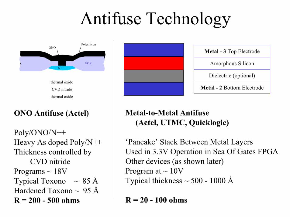
Antifuse TechnologyPolysilicon
FOXN++
ONOMetal - 3 Top Electrode
Amorphous Silicon
Dielectric (optional)thermal oxide
Metal - 2 Bottom ElectrodeCVD nitride
thermal oxide
Metal-to-Metal Antifuse(Actel, UTMC, Quicklogic)
‘Pancake’ Stack Between Metal LayersUsed in 3.3V Operation in Sea Of Gates FPGAOther devices (as shown later)Program at ~ 10VTypical thickness ~ 500 - 1000 Å
R = 20 - 100 ohms
ONO Antifuse (Actel)
Poly/ONO/N++Heavy As doped Poly/N++Thickness controlled by
CVD nitridePrograms ~ 18VTypical Toxono ~ 85 ÅHardened Toxono ~ 95 ÅR = 200 - 500 ohms

Antifuse Cross-Sections
Amorphous Silicon(Vialink)
ONO(Act 1)
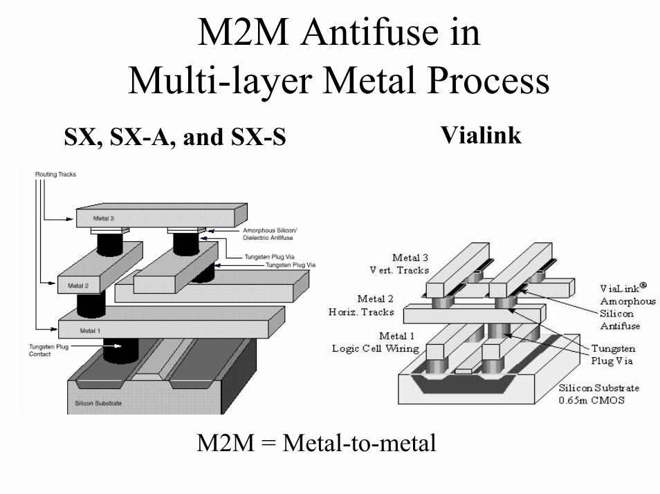
M2M Antifuse inMulti-layer Metal Process
VialinkSX, SX-A, and SX-S
M2M = Metal-to-metal
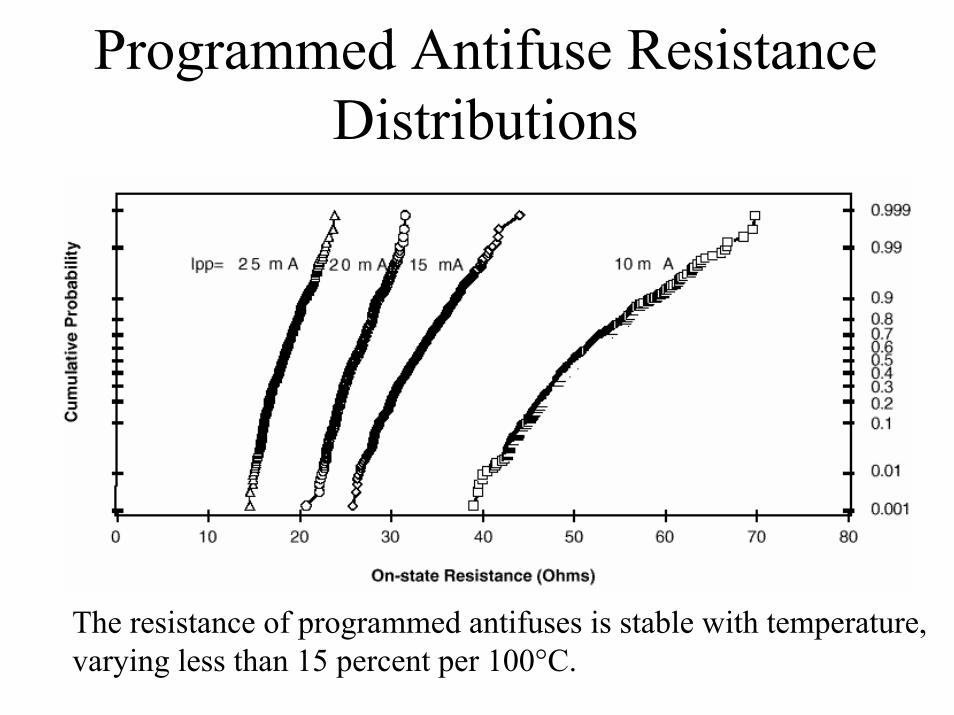
Programmed Antifuse Resistance Distributions
The resistance of programmed antifuses is stable with temperature,varying less than 15 percent per 100°C.

SRAM Switch Technology
Configuration Memory Cell
Read or WriteData Routing Connections

Xilinx 4000XL Series FPGAs
Gate Count (k Gates)0 20 40 60 80 100
Bits
100x100
1x10³
10x103
100x103
1x10⁶
10x106
Registers Max User Ram Configuration Bits
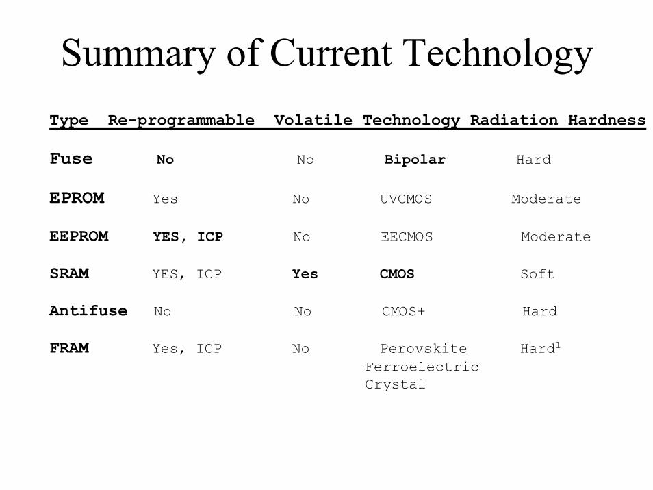
Summary of Current TechnologyType Re-programmable Volatile Technology Radiation Hardness
Fuse No No Bipolar Hard
EPROM Yes No UVCMOS Moderate
EEPROM YES, ICP No EECMOS Moderate
SRAM YES, ICP Yes CMOS Soft
Antifuse No No CMOS+ Hard
FRAM Yes, ICP No Perovskite Hard1
FerroelectricCrystal
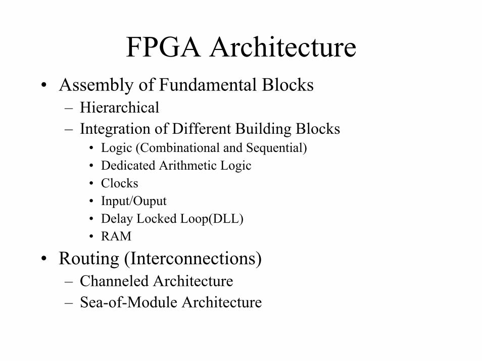
FPGA Architecture• Assembly of Fundamental Blocks
– Hierarchical– Integration of Different Building Blocks
• Logic (Combinational and Sequential)• Dedicated Arithmetic Logic• Clocks• Input/Ouput• Delay Locked Loop(DLL)• RAM
• Routing (Interconnections) – Channeled Architecture– Sea-of-Module Architecture

Channel Architecture
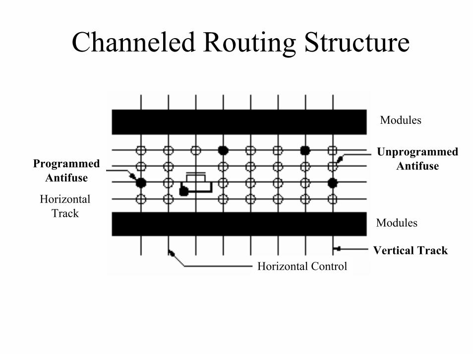
Channeled Routing Structure
Horizontal Control
Modules
UnprogrammedAntifuseProgrammed
Antifuse
HorizontalTrack
Modules
Vertical Track

Act 3 Architecture Detail
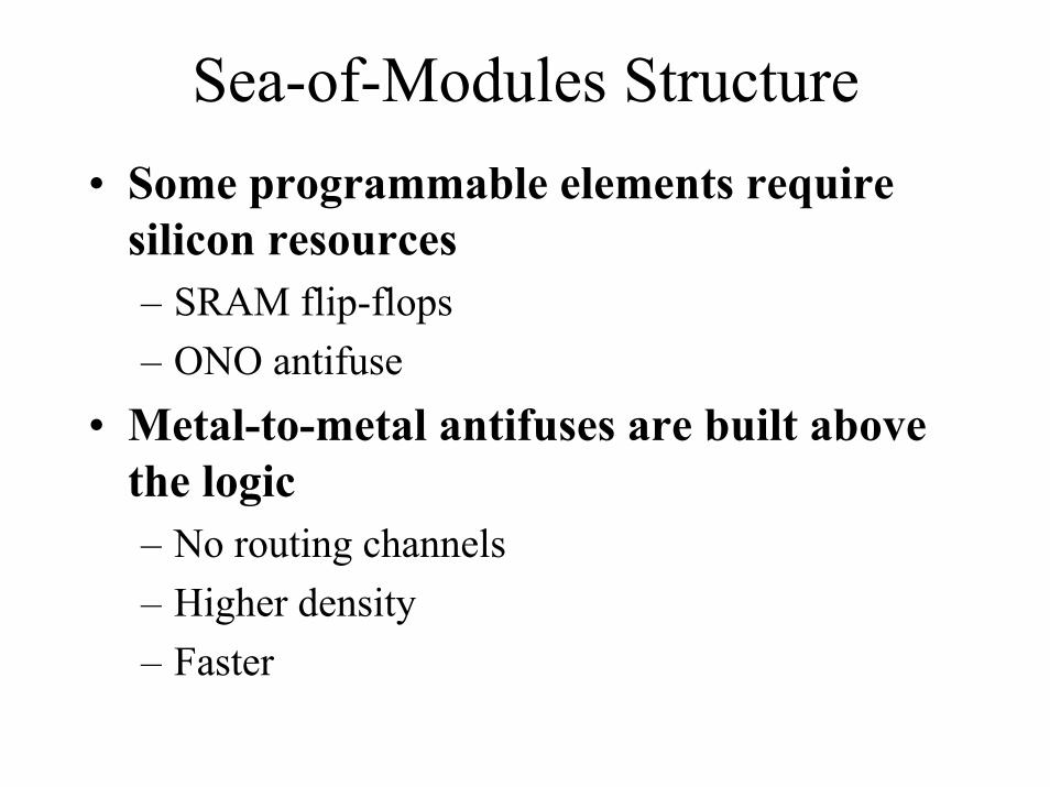
Sea-of-Modules Structure• Some programmable elements require
silicon resources– SRAM flip-flops– ONO antifuse
• Metal-to-metal antifuses are built above the logic– No routing channels– Higher density– Faster
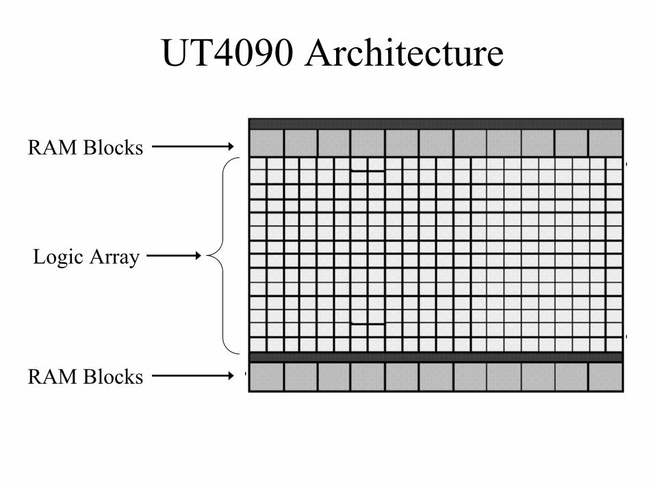
UT4090 Architecture
RAM Blocks
Logic Array
RAM Blocks
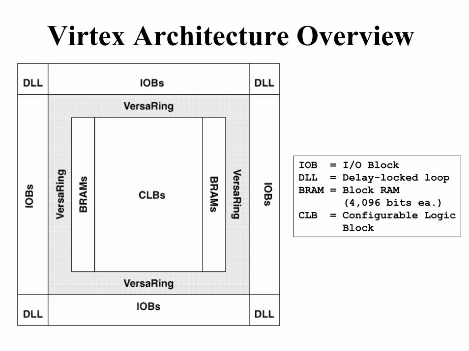
Virtex Architecture Overview
IOB = I/O BlockDLL = Delay-locked loopBRAM = Block RAM
(4,096 bits ea.)CLB = Configurable Logic
Block
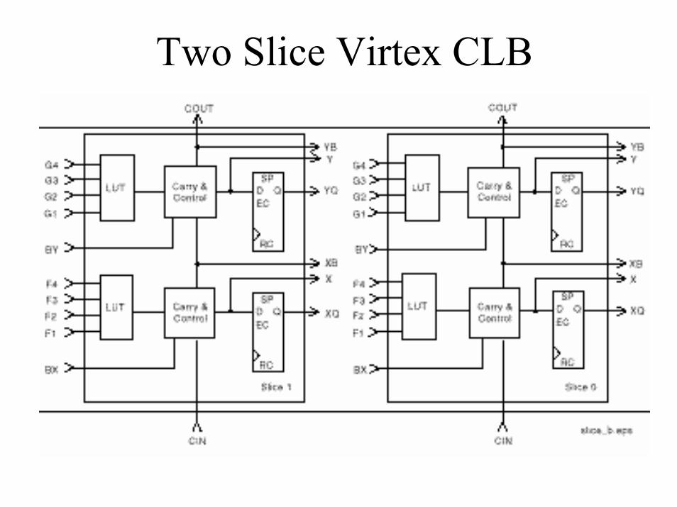
Two Slice Virtex CLB

Logic Modules• Actel (Act 1,2,3, SX)
– Basics– Flip-flop Construction
• UTMC/Quicklogic (i.e., UT4090)– RAM blocks
• Xilinx (i.e., CQR40xxXL, Virtex,VirtexII)– LUTs/ BlockRAM– Carry Logic/Chain
• Mission Research Corp. (MRC) - Orion• Atmel - AT6010
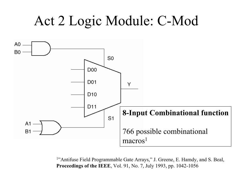
Act 2 Logic Module: C-Mod
8-Input Combinational function
766 possible combinationalmacros1
1”Antifuse Field Programmable Gate Arrays,” J. Greene, E. Hamdy, and S. Beal,Proceedings of the IEEE, Vol. 91, No. 7, July 1993, pp. 1042-1056

Act 2 Flip-flop ImplementationFeedback goes through
antifuses (R) and routingsegments (C)
Hard-wired Flip-flop Routed or “C-C Flip-flop”
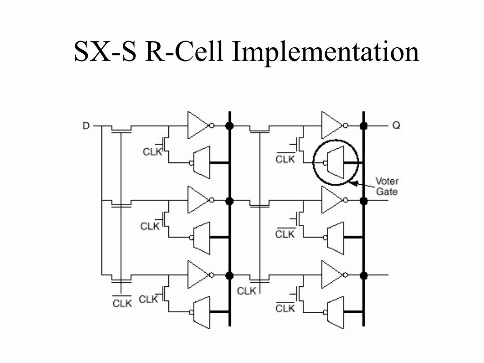
SX-S R-Cell Implementation

UT4090 Logic Module
• Antifuse Configuration Memory
• Mux-based• Multiple Outputs• Wide logic functions
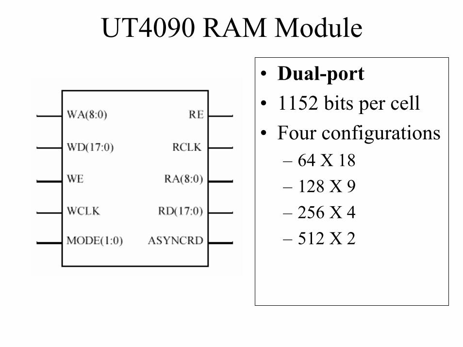
UT4090 RAM Module• Dual-port• 1152 bits per cell• Four configurations
– 64 X 18– 128 X 9– 256 X 4– 512 X 2

XC4000 Series CLBSimplified CLB - Carry Logic Not Shown
RAM LUTsfor Logic orsmall SRAM Two Flip-flops

XQR4000XL Carry Path
Placement is important for performance.
General interconnect
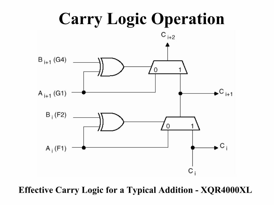
Carry Logic Operation
Effective Carry Logic for a Typical Addition - XQR4000XL

MRC Orion Logic Module

AT60xx Logic Module
Memory Architecture
• Radiation-hardened PROM• Configuration Memory• EEPROM
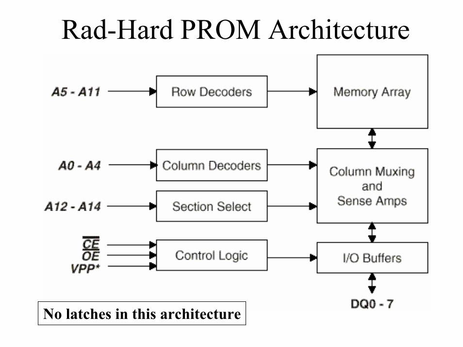
Rad-Hard PROM Architecture
No latches in this architecture
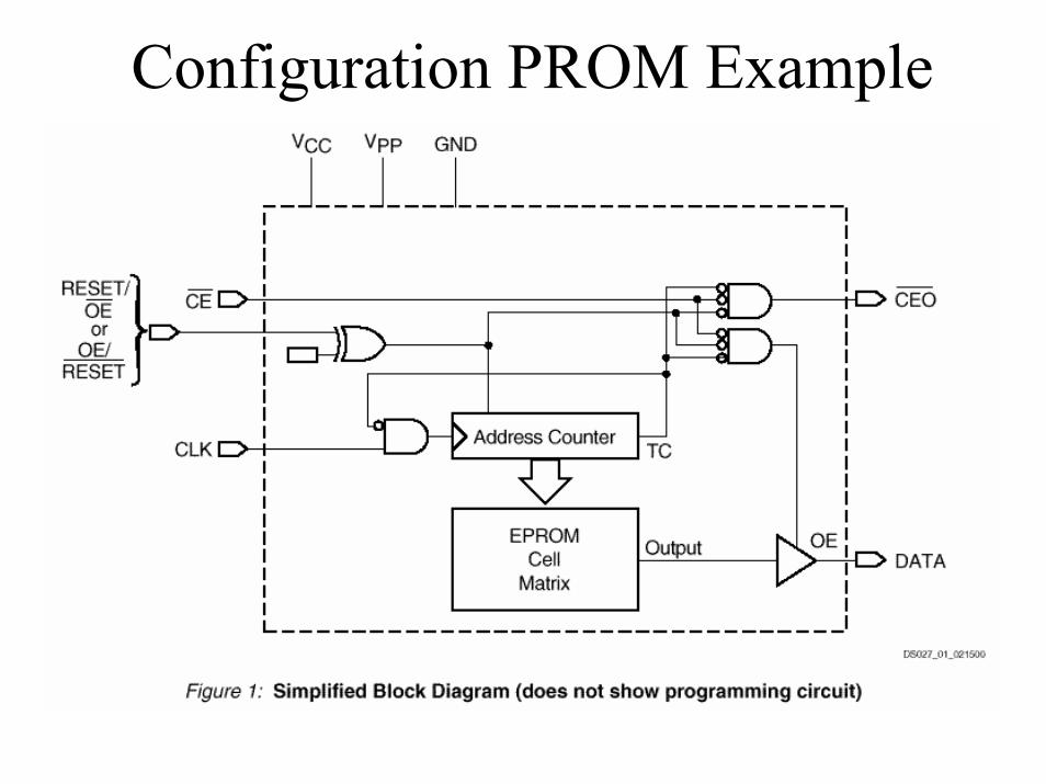
Configuration PROM Example

W28C64 EEPROMSimplified Block Diagram
RowAddressLatches
ColumnAddressLatches
RowAddressDecoder
ColumnAddressDecoder
EdgeDetect &Latches
ControlLatch
ControlLogic
64 BytePage
Buffer
Timer
E2
MemoryArray
I/O Buffer/Data Polling
A6-12
A0-5
CE*
WE*
Latch Enable
OE*
CLK VW I/O0-7PE RSTB
Input/Output ModulesA Brief Overview
• Basic Input/Output (I/O) Module• Some Features
– Slew Rate Control– Different I/O Standards– Input Delays– Banks
• Deterministic Powerup• Cold Sparing
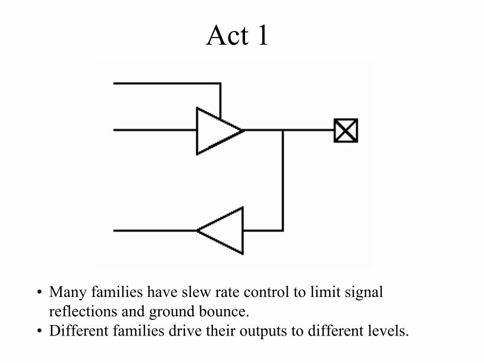
Act 1
• Many families have slew rate control to limit signal reflections and ground bounce.
• Different families drive their outputs to different levels.

Different I/O Standards Virtex 2.5V Example
I/O Standard Input Ref Output Board 5VVoltage Source Termination Tolerant(VREF) Voltage Voltage
(VCCO) (VTT)LVTTL 2–24 mA N/A 3.3 N/A YesLVCMOS2 N/A 2.5 N/A YesPCI, 5 V N/A 3.3 N/A YesPCI, 3.3 V N/A 3.3 N/A NoGTL 0.8 N/A 1.2 NoGTL+ 1.0 N/A 1.5 NoHSTL Class I 0.75 1.5 0.75 NoHSTL Class III 0.9 1.5 1.5 NoHSTL Class IV 0.9 1.5 1.5 NoSSTL3 Class I &II 1.5 3.3 1.5 NoSSTL2 Class I & II 1.25 2.5 1.25 NoCTT 1.5 3.3 1.5 NoAGP 1.32 3.3 N/A No
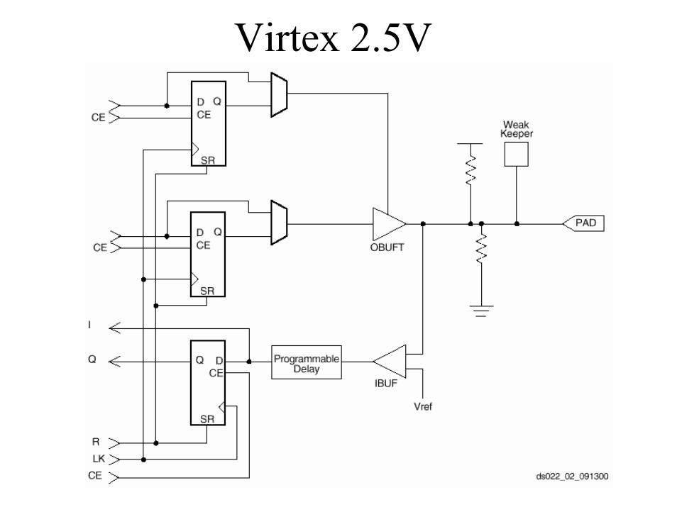
Virtex 2.5V

Deterministic Power-upSX-S Example
PRE
CLR
VCCI
RTSX-S
Pull-down enabled
Pull-up enabled
• Pull-ups /downs are selectable on an individual I/O basis
• Pull-up follows VCCI
• Pull-downs and pull-ups are dis-abled 50 ns after VCCA reaches 2.5V and therefore do not draw current during regular operation.
• Once VCCA is powered-up, 50ns is required for a valid signal to propagate to the outputs before the pull-ups /downs are disabled
VCCA
Input Driven low or external POR Signal

Cold Sparing - SX-S
RTSX-S
VCCI
GND
0 VoltsRTSX-S
VCCI
GND
3.3/5 Volts
Active Bus or Backplane
Powered-downBoard
Powered-upBoard
I/O w/ ” Hot-Swap”Enabled does not
sink current
Packaging and Mechanical Aspects
• Package Types– Dual In-line Package (DIPs)– Flatpacks– Pin Grid Arrays (PGAs)– Ceramic Quad Flat Packs (CQFP)– Plastic Quad Flat Pack (PQFP)
• Plastic Package Qualification• Lead/Ball Pitch• Mass Characteristics• Shielding

Flat PackNorthrop-Grumman 256k EEPROM

Shielded Packages - Rad-Pak™
• This package, with tie bar, 24 grams• Shielding thickness may vary between lots• Shield is 10-90/copper-tungsten• Density of shield is ~ 18 g/cm3 (need to verify)• EEPROMs and other devices also packaged similarly

Spot Shielding Qualification Board - Maximum Thickness
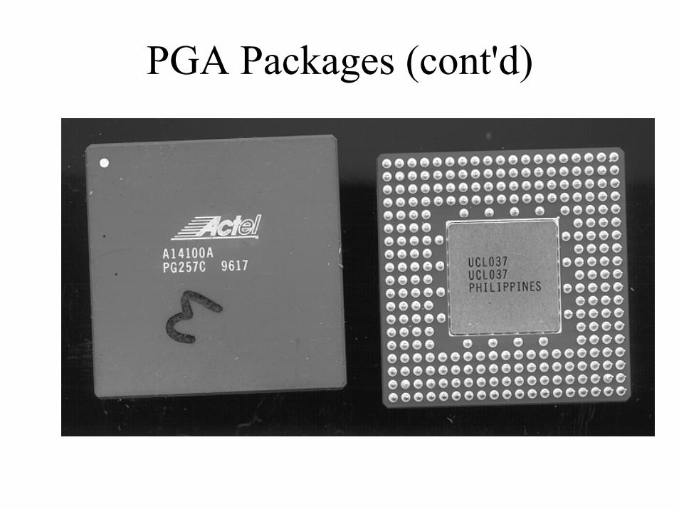
PGA Packages (cont'd)

PQFP Package
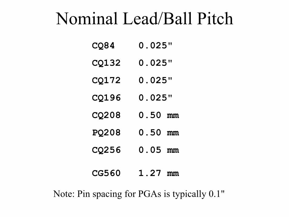
Nominal Lead/Ball PitchCQ84 0.025"
CQ132 0.025"
CQ172 0.025"
CQ196 0.025"
CQ208 0.50 mm
PQ208 0.50 mm
CQ256 0.05 mm
CG560 1.27 mm
Note: Pin spacing for PGAs is typically 0.1"

Mass CharacteristicsApproximate values (in grams)
PG84 8.0
PG133 11.0
PG176 19.0
PG207 24.5
PG257 27.3
CQ84 2.2
CQ132 5.8
CQ172 8.8
CQ196 11.1
CQ208 8.8CQ208 18.5PQ208 5.2 CB228 17.6CQ256 13.0CQ256 20.2
1
1BG560 11.5CG560 11.5
1With heat sink. Over the years, there has been a lot of variation as to which parts have heat sinks. Check each package.

Reliability
• Introduction to Reliability• Historical Perspective• Current Devices• Trends
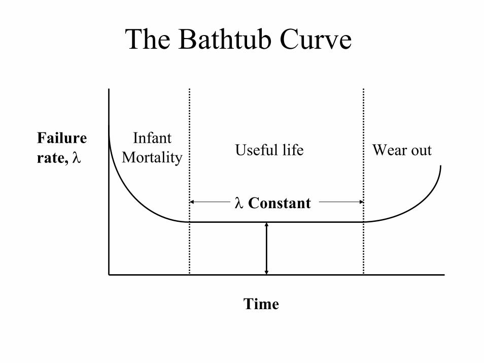
The Bathtub Curve
Time
Failurerate, λ
λ Constant
Useful life Wear outInfant
Mortality
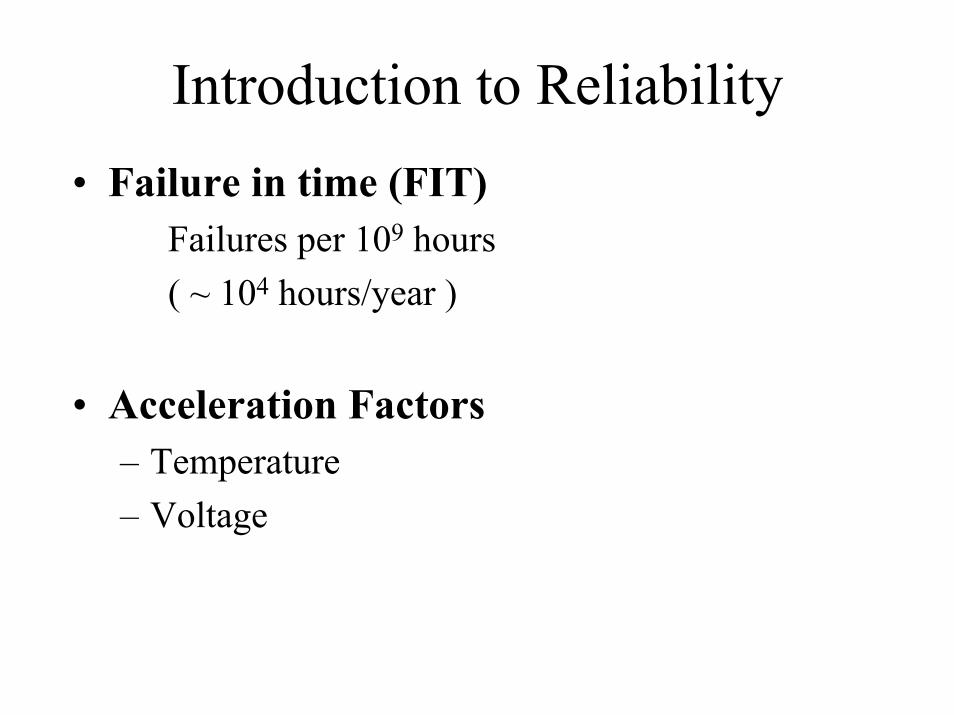
Introduction to Reliability• Failure in time (FIT)
Failures per 109 hours( ~ 104 hours/year )
• Acceleration Factors– Temperature– Voltage

Introduction to Reliability (cont'd)
Most failure mechanisms can be modeled using the Arrhenius equation.
ttf - time to failure (hours)C - constant (hours)EA - activation energy (eV)k - Boltzman's constant (8.616 x 10⁻⁵eV/°K)T - temperature (ºK)
ttf = C • eEA/kT
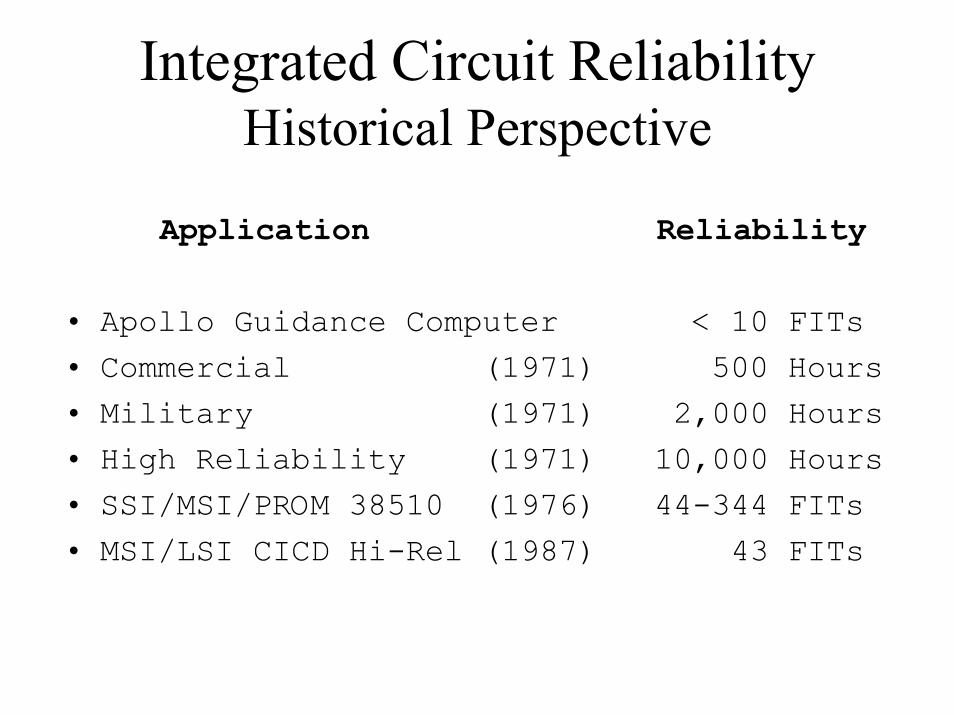
Integrated Circuit ReliabilityHistorical Perspective
Application Reliability
• Apollo Guidance Computer < 10 FITs• Commercial (1971) 500 Hours• Military (1971) 2,000 Hours• High Reliability (1971) 10,000 Hours• SSI/MSI/PROM 38510 (1976) 44-344 FITs• MSI/LSI CICD Hi-Rel (1987) 43 FITs
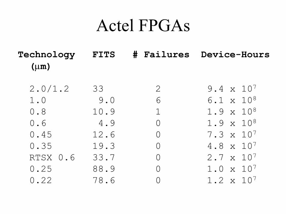
Actel FPGAsTechnology FITS # Failures Device-Hours(µm)
2.0/1.2 33 2 9.4 x 10⁷
1.0 9.0 6 6.1 x 10⁸
0.8 10.9 1 1.9 x 10⁸
0.6 4.9 0 1.9 x 10⁸
0.45 12.6 0 7.3 x 10⁷
0.35 19.3 0 4.8 x 107
RTSX 0.6 33.7 0 2.7 x 10⁷
0.25 88.9 0 1.0 x 10⁷
0.22 78.6 0 1.2 x 10⁷

Xilinx FPGAs
• XC40xxXL– Static: 9 FIT, 60% UCL– Dynamic: 29 FIT, 60% UCL
• XCVxxx(Virtex)– Static: 34 FIT, 60% UCL– Dynamic: 443 FIT, 60% UCL
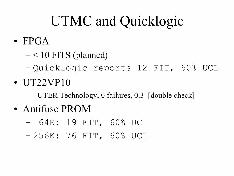
UTMC and Quicklogic• FPGA
– < 10 FITS (planned)– Quicklogic reports 12 FIT, 60% UCL
• UT22VP10UTER Technology, 0 failures, 0.3 [double check]
• Antifuse PROM– 64K: 19 FIT, 60% UCL
– 256K: 76 FIT, 60% UCL

Actel FIT Rate Trends
Thermal
• Thermal Analysis Basics• Summary of Package Characteristics• Package Considerations
– Cavity Up/Down– Heat Sinks

Thermal Performance• Package modeled as a resistance
• Junction temperature the critical parameter– Often derated to ~ 100 ºC
• tJ = P • θJ-C
tJ = Junction temperature in ºCP = Power in wattsθJ-C = thermal resistance, junction to case, in ºC/watt
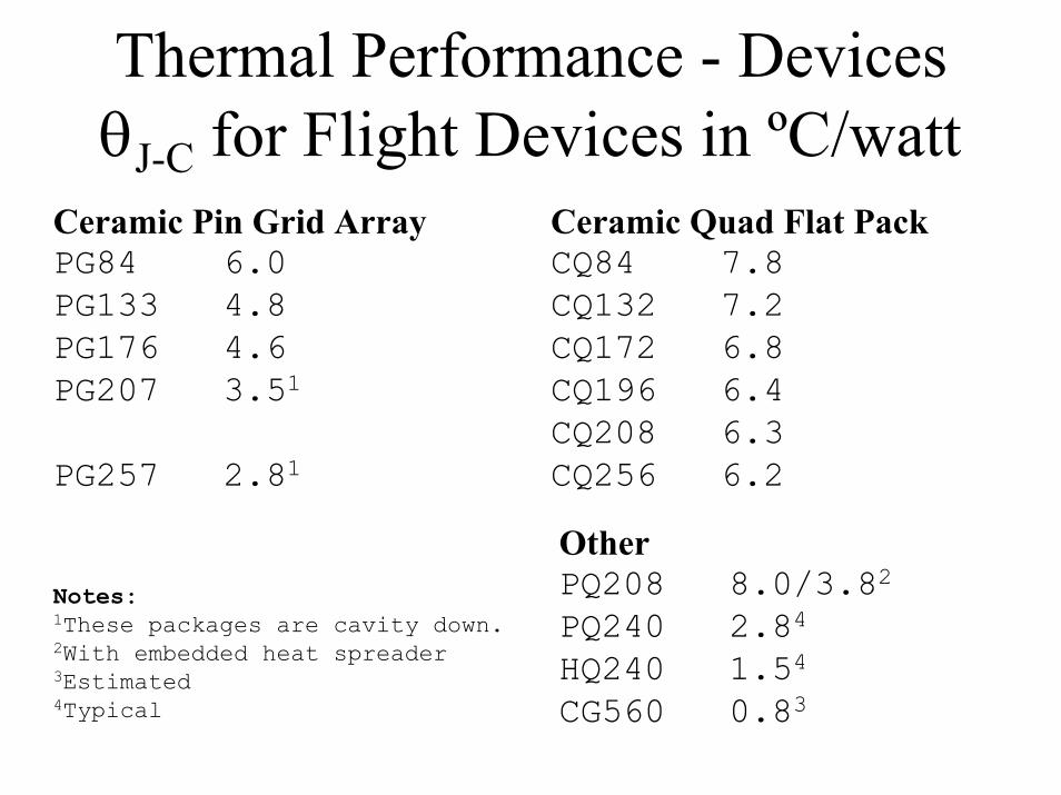
Thermal Performance - DevicesθJ-C for Flight Devices in ºC/watt
Ceramic Pin Grid ArrayPG84 6.0PG133 4.8PG176 4.6PG207 3.51
PG257 2.81
Notes:1These packages are cavity down.2With embedded heat spreader3Estimated4Typical
Ceramic Quad Flat PackCQ84 7.8CQ132 7.2CQ172 6.8CQ196 6.4CQ208 6.3CQ256 6.2
OtherPQ208 8.0/3.82
PQ240 2.84
HQ240 1.54
CG560 0.83
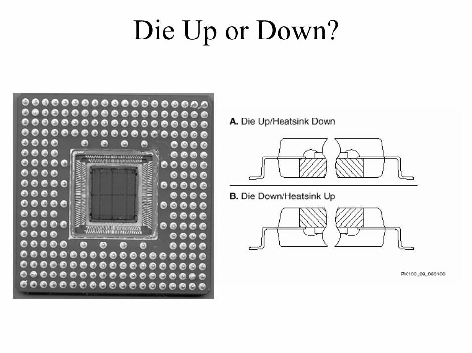
Die Up or Down?

CQFP256 w/ Heat Sink
Speed/Performance
• Basic Delay Model and Components• Sample Delays
– Examples from different families• Hard-wired Structures
– Routing– Arithmetic Logic

Antifuse Delay Model
Tau = Resistance * Capacitance
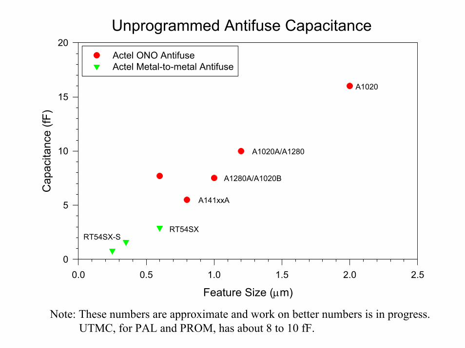
Unprogrammed Antifuse Capacitance
Feature Size (µm)0.0 0.5 1.0 1.5 2.0 2.5
Cap
acita
nce
(fF)
0
5
10
15
20Actel ONO AntifuseActel Metal-to-metal Antifuse
RT54SX-SRT54SX
A1280A/A1020B
A141xxA
A1020A/A1280
A1020
Note: These numbers are approximate and work on better numbers is in progress.UTMC, for PAL and PROM, has about 8 to 10 fF.
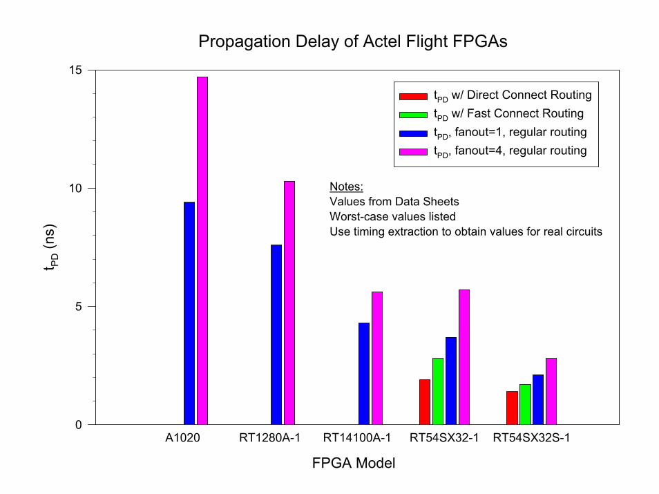
Propagation Delay of Actel Flight FPGAs
FPGA Model
A1020 RT1280A-1 RT14100A-1 RT54SX32-1 RT54SX32S-1
t PD (n
s)
0
5
10
15
tPD w/ Direct Connect RoutingtPD w/ Fast Connect RoutingtPD, fanout=1, regular routingtPD, fanout=4, regular routing
Notes:Values from Data SheetsWorst-case values listedUse timing extraction to obtain values for real circuits
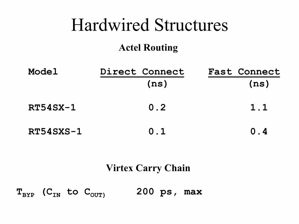
Hardwired StructuresActel Routing
Model Direct Connect Fast Connect(ns) (ns)
RT54SX-1 0.2 1.1
RT54SXS-1 0.1 0.4
Virtex Carry Chain
TBYP (CIN to COUT) 200 ps, max
Power Consumption
• Power Basics• Quiescent (Static) Current• Dynamic Current
– Per logic module– Clock tree
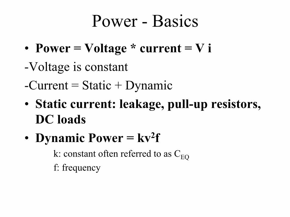
Power - Basics• Power = Voltage * current = V i-Voltage is constant-Current = Static + Dynamic• Static current: leakage, pull-up resistors,
DC loads• Dynamic Power = kv2f
k: constant often referred to as CEQ
f: frequency
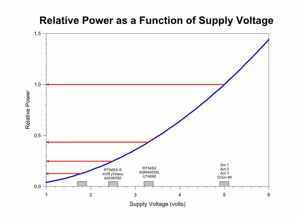
Relative Power as a Function of Supply Voltage
Supply Voltage (volts)
1 2 3 4 5 6
Rel
ativ
e Po
wer
0.0
0.5
1.0
1.5
Act 1Act 2Act 3
Orion-4K
RT54SXXQR4000XL
UT4090
RT54SX-SXVR (Virtex)A500K050

Device (Array) Quiescent Current1
Device Voltage Typical Spec LevelType (V) ICC (mA) ICCMAX(mA)
A500K050 2.5 < 1 102
Orion-4K 5.0RT1020 5.0 < 1 20RT1280A 5.0 < 1 20RT14100A 5.0 < 1 20RT54SX32 3.3 < 1 25RT54SX32S 2.5 < 1 25UT4090 3.3 5XQR40xxXL 3.3 20XQV100 2.5 50XQV300 2.5 75XQV600 2.5 100XQV1000 2.5 100AT6010
1No DC Loads2Commercial Specification
XQV600 Lot Data (mA)1
lot # min mean max
1157448 4.72 6.41 8.131152401 6.26 8.37 11.401139803 3.75 5.57 12.85
1commercial or industrial worst-case, checking

PROM Device Current1
Device Voltage Standby Dynamic @F (MHz)Type (V) ICC (mA) ICCMAX(mA)
UT28F64 5.0 0.5 100 28.62
UT28F256 5.0 < 2 125 28.62
197A8073 5.0 2.0 200 22.2
1Specification levels2Derates @ 2.5 mA/MHz3BAE Systems (formerly Lockmart) 32kx8 PROM
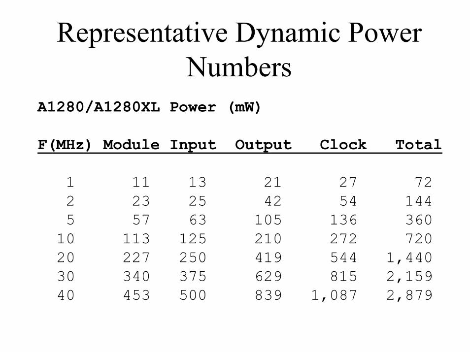
Representative Dynamic Power Numbers
A1280/A1280XL Power (mW)
F(MHz) Module Input Output Clock Total
1 11 13 21 27 722 23 25 42 54 1445 57 63 105 136 36010 113 125 210 272 72020 227 250 419 544 1,44030 340 375 629 815 2,15940 453 500 839 1,087 2,879

Power Consumption (Logic Module)
Device TypeAct 1 Act 2 Act 3 RTSX RTSX-S
Pow
er (µ
w/M
Hz)
0
50
100
150
200
250
Notes:1. Based on data sheets2. Nominal voltages used for calculations3. SX data is "Preliminary"4. SX-S data is "Advanced"

A Brief Introduction to Radiation and Programmable Devices

Types of Radiation Effects• Total Dose• Single Event Effects (SEE)
– Single Event Upset (SEU)• Multiple Bit Upset (MBU)
– Single Event Latchup (SEL)– Single Event Transient (SET)– Antifuse and Rupture– Loss of Functionality– Snap back
• Protons• Miscellaneous

Total Dose
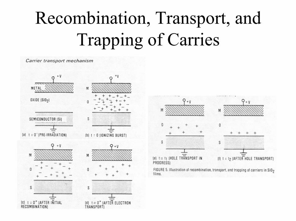
Recombination, Transport, and Trapping of Carries
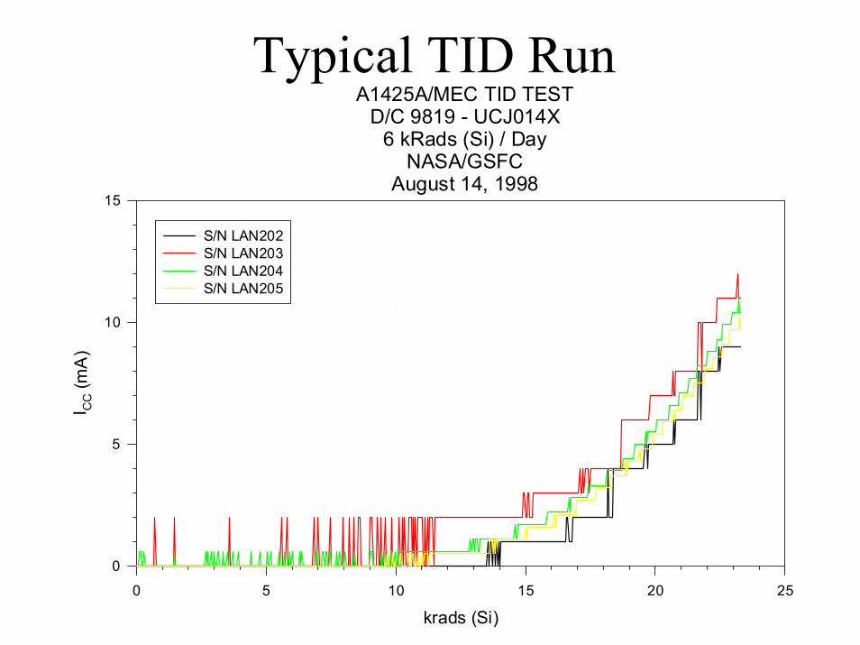
A1425A/MEC TID TESTD/C 9819 - UCJ014X
6 kRads (Si) / DayNASA/GSFC
August 14, 1998
krads (Si)0 5 10 15 20 25
I CC (m
A)
0
5
10
15
S/N LAN202S/N LAN203S/N LAN204S/N LAN205
Typical TID Run
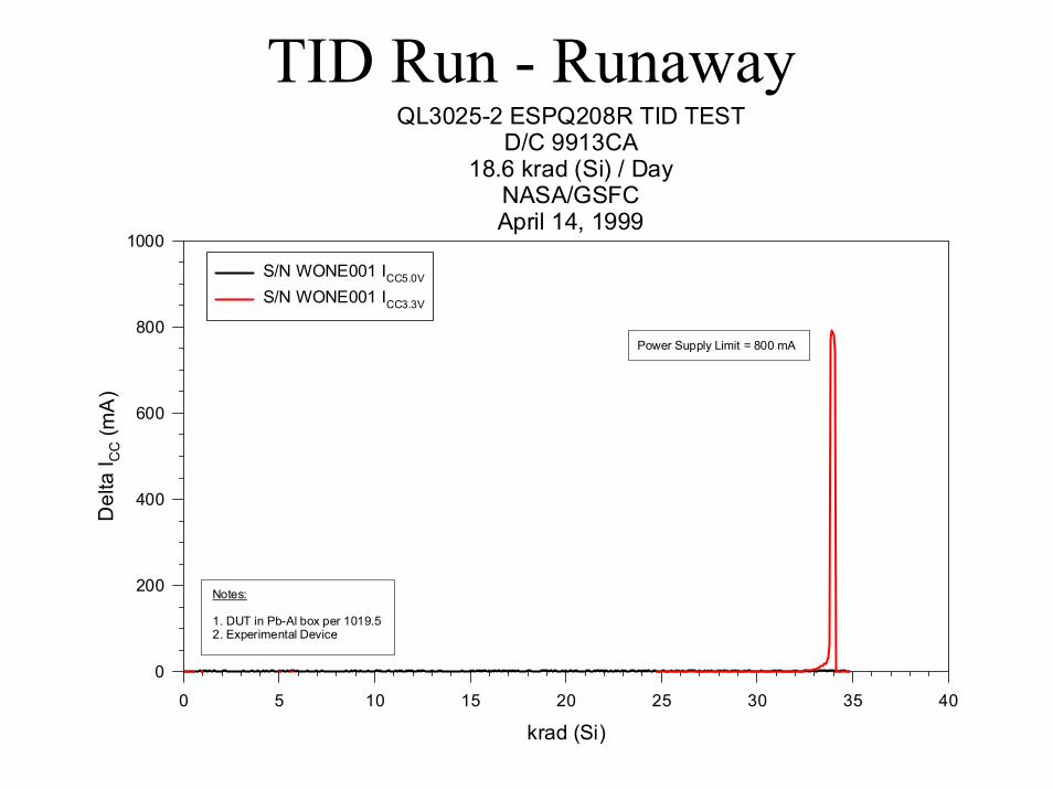
TID Run - RunawayQL3025-2 ESPQ208R TID TEST
D/C 9913CA18.6 krad (Si) / Day
NASA/GSFCApril 14, 1999
krad (Si)0 5 10 15 20 25 30 35 40
Del
ta I C
C (m
A)
0
200
400
600
800
1000
S/N WONE001 ICC5.0V
S/N WONE001 ICC3.3V
Power Supply Limit = 800 mA
Notes:
1. DUT in Pb-Al box per 1019.52. Experimental Device
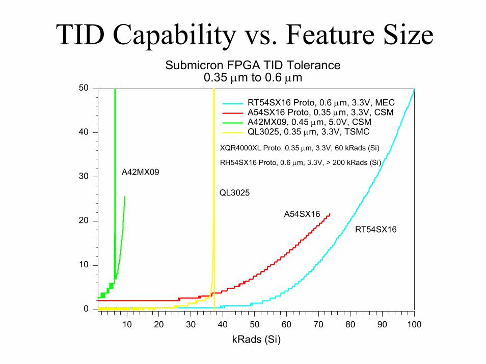
TID Capability vs. Feature SizeSubmicron FPGA TID Tolerance
0.35 µm to 0.6 µm
kRads (Si)10 20 30 40 50 60 70 80 90 100
0
10
20
30
40
50
RT54SX16 Proto, 0.6 µm, 3.3V, MECA54SX16 Proto, 0.35 µm, 3.3V, CSMA42MX09, 0.45 µm, 5.0V, CSMQL3025, 0.35 µm, 3.3V, TSMC
QL3025
A54SX16
RT54SX16
A42MX09
XQR4000XL Proto, 0.35 µm, 3.3V, 60 kRads (Si)
RH54SX16 Proto, 0.6 µm, 3.3V, > 200 kRads (Si)
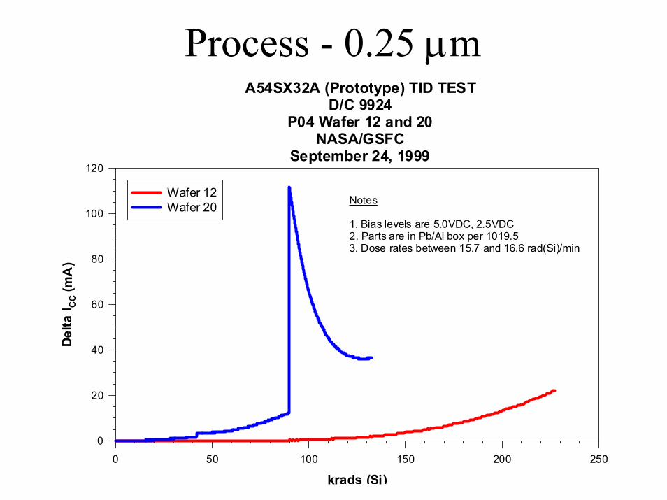
Process - 0.25 µmA54SX32A (Prototype) TID TEST
D/C 9924P04 Wafer 12 and 20
NASA/GSFCSeptember 24, 1999
krads (Si)0 50 100 150 200 250
Delta
I CC (m
A)
0
20
40
60
80
100
120
Wafer 12Wafer 20 Notes
1. Bias levels are 5.0VDC, 2.5VDC2. Parts are in Pb/Al box per 1019.53. Dose rates between 15.7 and 16.6 rad(Si)/min

Single Event Upset(SEU)
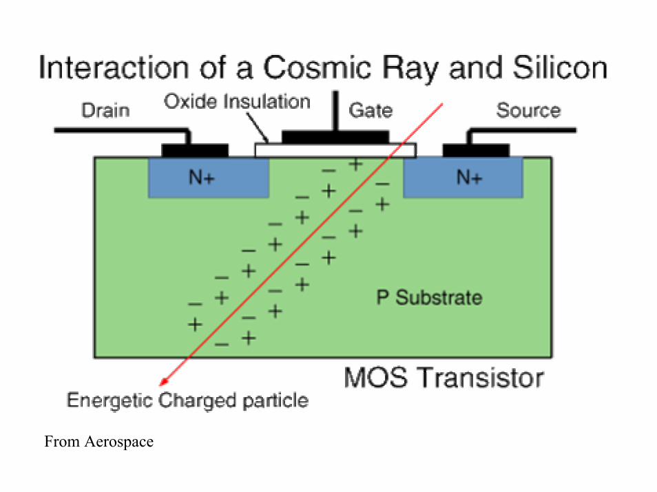
From Aerospace
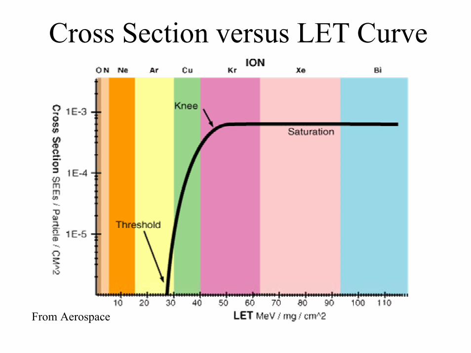
Cross Section versus LET Curve
From Aerospace
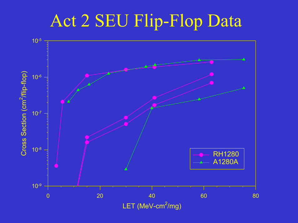
Act 2 SEU Flip-Flop Data
LET (MeV-cm2/mg)0 20 40 60 80
Cro
ss S
ectio
n (c
m2 /fl
ip-fl
op)
10-9
10-8
10-7
10-6
10-5
RH1280 A1280A
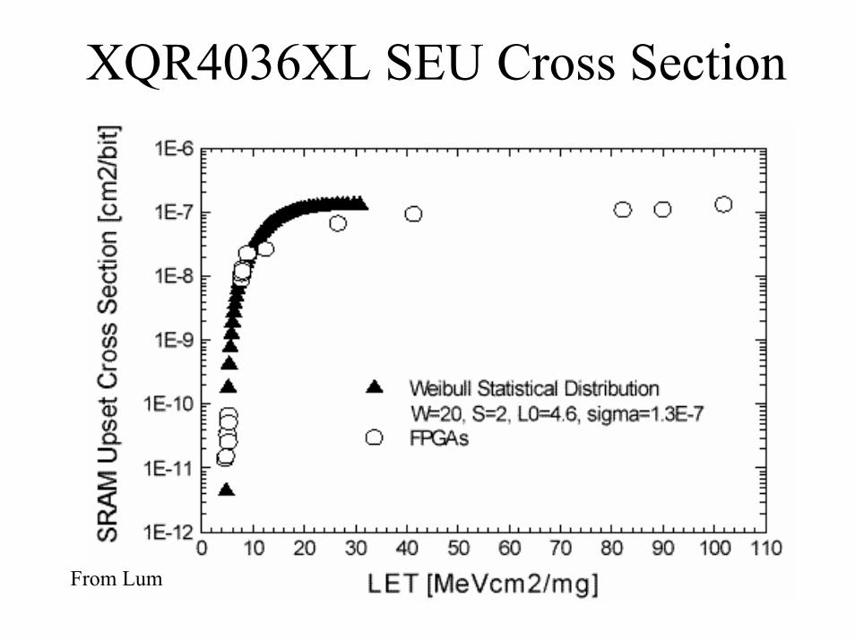
XQR4036XL SEU Cross Section
From Lum
Single Event Latchup(SEL)
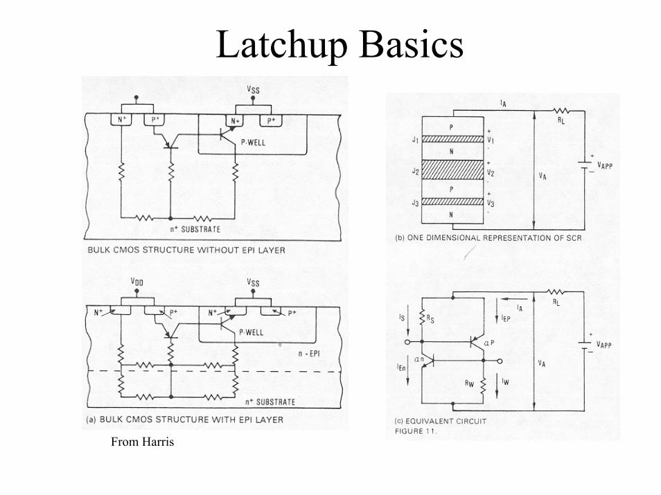
Latchup Basics
From Harris

SEL - QL3025 0.35 µm
Time (Sec)
0 5 10 15 20
I CC (m
A)
0
100
200
300
400
500BNL 02/98S/N QL1 Run T2VBIAS = 5.0V, 3.3VTitanium @ 0 DegLET = 18.8 MeV-cm2/mg
Antifuse and Rupture

RH1280 S/N 063 Antifuse Rupture
Fluence (ions/cm2)
0 20x106 40x106 60x106 80x106 100x106
Icc
(mA)
30
35
40
45
VCC = 4.7 VDC; LET = 53; Angle = 0 Degrees
Technology Development VehicleComparison of Rupture Currents
Ion = Iodine
Time (Sec)18 20 22 24 26 28 30 32 34 36 38 40
I CC
3.3(
mA
)
2
4
6
8
10
12
14
16
18
20
Amorphous SiliconAntifuse RuptureONO Antifuse
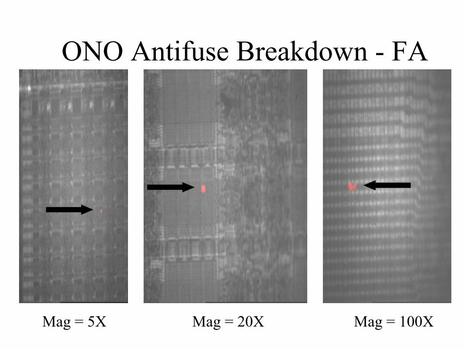
ONO Antifuse Breakdown - FA
Mag = 5X Mag = 20X Mag = 100X

Protons

ICC Damage During Proton TestingASIC and Antifuse FPGAQYH530 193 MeV Proton Test
Flux = 1 x 10⁹ p/cm2/SecS/N QYHD2 - DITS-2 Lot
NASA/GSFCJune 17, 1997
kRads (Si)0 5 10 15 20 25
Del
ta I C
C (m
A)
0
10
20
30
40
Note: Device Previously Irradiated for Heavy Ion Testing
QL3025 Proton IrradiationS/N QL6
June, 1998Indiana University Cyclotron
NASA/GSFC
kRads (Si)
0 5 10 15 20 25 30 35
I CC
3.3 (
mA
)
1
10
100
1000
Note: Different scales for each run.

RH1280 Proton Upsets
From Lockheed-Martin/Actel

Summary

FRAM Memory Functionality Loss During Heavy Ion Test
Time (s)0 50 100 150 200 250
I CC (m
A)
0
1
2
3
4
5
6
7
Strip chart of FM1608 (research fab) current during heavy ion irradiation. The device lost functionality during the test while the current decreased from it's normal dynamic levels of approximately 6.3 mA to it's quiescent value, near zero. The device recovered functionally and operated normally throughout the latter part of the test. This effect was seen at least three times during the limited testing of this device.