properties of fluorescent semiconductor …michalet/papers/sm2001.pdf262 single molecules review...
TRANSCRIPT
© WILEY-VCH Verlag Berlin GmbH, 13086 Berlin, 2001 1438-5163/01/0211-0261 $ 17.50+.50/0
261
Single Mol. 2 (2001) 4, 261-276 REVIEW ARTICLE MoleculesSingle
Properties of Fluorescent SemiconductorNanocrystals and their Application to BiologicalLabeling
Xavier Michalet 1,2,4), Fabien Pinaud 1,2,4), Thilo D. Lacoste 1,2,5), MaximeDahan 1,2,6), Marcel P. Bruchez 3,7), A. Paul Alivisatos 1,3) and Shimon Weiss 1,2,4)
1) Material Sciences Division , Lawrence Berkeley NationalLaboratory, 1 Cyclotron Road, Berkeley, CA 94720, USA
2) Physical Biosciences Division, Lawrence Berkeley NationalLaboratory, 1 Cyclotron Road, Berkeley, CA 94720, USA
3) Department of Chemistry, University of California,Berkeley, CA 94720, USA
4) Department of Chemistry and Biochemistry/Department ofPhysiology, University of California, Los Angeles, CA90095, USA
5) Present address:LifeBits AG, Albrechtstr. 9, 72072Tuebingen, Germany
6) Present address: Laboratoire Kastler Brossel, EcoleNormale Supérieure, 24, rue Lhomond, 75731 ParisCedex 5, France
7) Present address: Quantum Dot Corp., 26118 ResearchRoad, Hayward, CA 94545, USA
Correspondence toXavier MichaletMaterial Sciences DivisionLawrence Berkeley National Laboratory1 Cyclotron Road, Berkeley, CA 94720, USAtel +1 (510)-486-4041fax + 1 (510)-486-5530email [email protected], [email protected]
submitted 15 Aug 2001accepted 22 Nov 2001published 30 Nov 2001
Abstract
We review recent advances in the development of colloidalfluorescent semiconductor nanocrystals (a class of quantumdots) for biological labeling. Although some of thephotophysical properties of nanocrystals are not fullyunderstood and are still actively investigated, researchershave begun developing bioconjugation schemes andapplying such probes to biological assays. Nanocrystalspossess several qualities that make them very attractive forfluorescent tagging: broad excitation spectrum, narrowemission spectrum, precise tunability of their emissionpeak, longer fluorescence lifetime than organic fluorophoresand negligible photobleaching. On the down side, theiremission is strongly intermittent ("blinking”) and their sizeis relatively large for many biological uses. We describehow to take advantage of nanocrystals’ spectral propertiesto increase the resolution of fluorescence microscopymeasurements down to the nanometer level. We also showhow their long fluorescence lifetime can be used to observemolecules and organelles in living cells without interferencefrom background autofluorescence, a pre-requisite for singlemolecule detectability. Finally, their availability in multicolorspecies and their single molecule sensitivity open upinteresting possibilities for genomics applications.
Introduction
Fluorescent semiconductor nanocystals (NC) properties andapplications stands amongst the most exciting researchfields in chemistry, physics and biology [1-5]. Theirdevelopment results from an increasing emphasis put onminiaturization in semiconductor physics. The first step

262 SingleMolecules REVIEW ARTICLE
Single Mol. 2 (2001) 4
towards nanometer scale happened in the field of layeredsemiconductor materials, known as heterostructures. Inthese two dimensional (2D) geometries [6], the epitaxialgrowth of precise atomic layers with controlled compositionusing molecular beam epitaxy [7-9] (MBE) allows to shapeand manipulate electronic wavefunctions in the solid at will,giving rise to rich phenomena such as resonant tunneling,integer and fractional quantum Hall effects, quantumconfinement, efficient lasing and many more (1973, 1985and 1998 Nobel Prizes in physics) [10]. The concept ofquantum confinement by band-gap engineering ofheterostructures was then extended to lower dimensions(1D and 0D) [11]. In the last two decades, we havewitnessed tremendous progress in the ability to synthesizequantum wells [12,13], wires [14] and dots [15,16] withhigh-speed, high-efficiency electronics and optoelectronicsdevices (information technology) being the main drive.
Quantum confinement arises when one of thedimensions L of the object becomes of the order of theexciton Bohr radius:
aex m eex= κh2
2 (1)
were κ is the semiconductor permittivity, mex is the reducedexciton mass, and e the electron charge (for example, aCuCl
= 7 Å, aGaAs = 100 Å and aCdSe = 56 Å).The most useful outcome of quantum confinement for
the applications discussed in this paper is the discretizationof the energy levels at the edges of the conduction andvalence bands upon dimensional reduction. The firstcontrolled synthesis and systematic studies of nanometersize semiconductor crystals in all three dimensions wereperformed by Ekimov and Éfros [17, 18]. They studiedquantum dot inclusions that were embedded in aninsulating glass matrix. The same types of material wereused long ago, at least since the Middle-Age, in stainedglass windows decorating churches with multicolorornaments. Ekimov’s sample was the first to exhibit thequantum-confined blue shift of the first absorption (exciton)peak, varying as a-2 (a being the nanocrystal radius) [17].Solving the effective Hamiltonian for a spherical geometry,Éfros and Éfros computed the electron and hole energies insuch a sphere and found a series of discrete lines,recovering the a-2 dependency observed in the experiment[18].
Another route to the synthesis of 0D semiconductorstructures was explored by several groups, who developedmethods for obtaining colloidal particle by diffusion-limitedgrowth in solvents [19-22] (for a review, see ref. [2]). Thesestudies were partly motivated by the mid-seventies energycrisis, which renewed the interest for devices capable of anefficient utilization of solar energy. Colloidal suspensions ofsemiconductor nanocrystals looked as promising electron orhole donors (catalysts), due to their large surface area tovolume ratio [19-21, 23-25]. A side product of these workswas the exploration of their luminescent properties, and in
particular the relationship between nanocrystal size andfluorescence properties [19,20,22,26]. Continuousimprovements have since then been reported [27-31], witha major advance being the addition of different composition,concentric heterostructure layers to the original "core”particle, a concept that was borrowed from "band gapengineering” developed for 2D MBE epitaxial growth [28,32-36]. This kind of research eventually took preeminencein the field, yielding to today’s applications in fluorescentbiological labeling [37-42] and possibly tomorrow’sapplications in tunable lasers [43] and flat panel displays[44-46].
Fluorescence of semiconductor nanocrystals is due tothe radiative recombination of an excited electron-hole pair.The resulting ensemble emission spectrum consists mainlyof a narrow Lorentzian band, 30-40 nm full width at halfmaximum (FWHM) slightly Stokes-shifted with respect to theexcitation band edge. The absorption spectrum, on theother hand is very broad, and contains quantumconfinement features. Both excitation and emission dependon the nanocrystallite size. These spectra are blue-shiftedas the nanocrystal diameter is reduced, due to the increasein exciton binding energy. Depending on the material, theirspectra can be continuously tuned from the UV-blue (ZnS[47], ZnSe [48]) to near infrared (CdS/HgS/CdS [32, 49],InP, InAs [50, 51]) through the visible (CdE, with E = S, Se,Te [29,52]).
This paper briefly reviews the synthesis and theimportant photophysical properties of fluorescentsemiconductor nanocrystals, which are of interest for theiruse as biological probes. We describe two applicationsdeveloped in our lab, multicolor imaging and ultrahighresolution colocalization that take advantage of theseunique photophysical properties. Finally, we review recentexamples of biological applications.
Nanocrystal Synthesis
Core Synthesis
Synthesis of semiconductor nanocrystals was initiallyperformed by precipitation from a solution containing themetal ion (Ag, Hg, Pb, Zn, Cd, In) by a hydroxide of S, Se, Teor P, followed by the addition of colloid stabilizers [19,20,22]. Further progress involved inverse micelle synthesis[27,28] leading to pure and stable powders of organicallycapped nanocrystals [2]. A further improvement involveshigh temperature (300 °C), surfactant synthesis startingfrom dimethyl-cadmium precursors in trioctylphosphineoxide (TOPO). The results are highly monodispersenanocrystals [29,52]. Recently, a simpler synthesis hasbeen devised using less toxic and reactive cadmium oxideprecursors that should allow scaling up the process [53,54]. The liquid phase is provided by a surfactant (TOPO),which is used together with trioctylphosphine (TOP) to coat
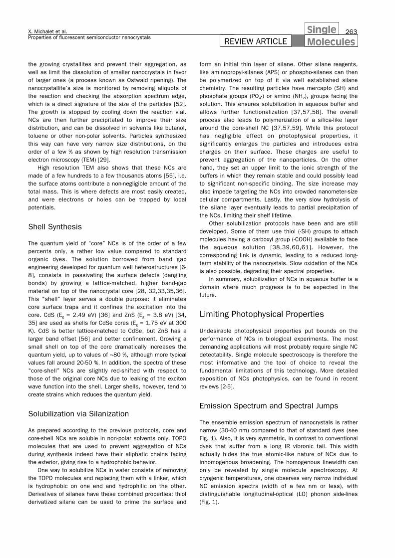
263
REVIEW ARTICLEX. Michalet et al.Properties of fluorescent semiconductor nanocrystals
SingleMolecules
the growing crystallites and prevent their aggregation, aswell as limit the dissolution of smaller nanocrystals in favorof larger ones (a process known as Ostwald ripening). Thenanocrystallite’s size is monitored by removing aliquots ofthe reaction and checking the absorption spectrum edge,which is a direct signature of the size of the particles [52].The growth is stopped by cooling down the reaction vial.NCs are then further precipitated to improve their sizedistribution, and can be dissolved in solvents like butanol,toluene or other non-polar solvents. Particles synthesizedthis way can have very narrow size distributions, on theorder of a few % as shown by high resolution transmissionelectron microscopy (TEM) [29].
High resolution TEM also shows that these NCs aremade of a few hundreds to a few thousands atoms [55], i.e.the surface atoms contribute a non-negligible amount of thetotal mass. This is where defects are most easily created,and were electrons or holes can be trapped by localpotentials.
Shell Synthesis
The quantum yield of "core” NCs is of the order of a fewpercents only, a rather low value compared to standardorganic dyes. The solution borrowed from band gapengineering developed for quantum well heterostructures [6-8], consists in passivating the surface defects (danglingbonds) by growing a lattice-matched, higher band-gapmaterial on top of the nanocrystal core [28, 32,33,35,36].This "shell” layer serves a double purpose: it eliminatescore surface traps and it confines the excitation into thecore. CdS (Eg = 2.49 eV) [36] and ZnS (Eg = 3.8 eV) [34,35] are used as shells for CdSe cores (Eg = 1.75 eV at 300K). CdS is better lattice-matched to CdSe, but ZnS has alarger band offset [56] and better confinement. Growing asmall shell on top of the core dramatically increases thequantum yield, up to values of ~80 %, although more typicalvalues fall around 20-50 %. In addition, the spectra of these"core-shell” NCs are slightly red-shifted with respect tothose of the original core NCs due to leaking of the excitonwave function into the shell. Larger shells, however, tend tocreate strains which reduces the quantum yield.
Solubilization via Silanization
As prepared according to the previous protocols, core andcore-shell NCs are soluble in non-polar solvents only. TOPOmolecules that are used to prevent aggregation of NCsduring synthesis indeed have their aliphatic chains facingthe exterior, giving rise to a hydrophobic behavior.
One way to solubilize NCs in water consists of removingthe TOPO molecules and replacing them with a linker, whichis hydrophobic on one end and hydrophilic on the other.Derivatives of silanes have these combined properties: thiolderivatized silane can be used to prime the surface and
form an initial thin layer of silane. Other silane reagents,like aminopropyl-silanes (APS) or phospho-silanes can thenbe polymerized on top of it via well established silanechemistry. The resulting particles have mercapto (SH) andphosphate groups (PO4-) or amino (NH2), groups facing thesolution. This ensures solubilization in aqueous buffer andallows further functionalization [37,57,58]. The overallprocess also leads to polymerization of a silica-like layeraround the core-shell NC [37,57,59]. While this protocolhas negligible effect on photophysical properties, itsignificantly enlarges the particles and introduces extracharges on their surface. These charges are useful toprevent aggregation of the nanoparticles. On the otherhand, they set an upper limit to the ionic strength of thebuffers in which they remain stable and could possibly leadto significant non-specific binding. The size increase mayalso impede targeting the NCs into crowded nanometer-sizecellular compartments. Lastly, the very slow hydrolysis ofthe silane layer eventually leads to partial precipitation ofthe NCs, limiting their shelf lifetime.
Other solubilization protocols have been and are stilldeveloped. Some of them use thiol (-SH) groups to attachmolecules having a carboxyl group (-COOH) available to facethe aqueous solution [38,39,60,61]. However, thecorresponding link is dynamic, leading to a reduced long-term stability of the nanocrystals. Slow oxidation of the NCsis also possible, degrading their spectral properties.
In summary, solubilization of NCs in aqueous buffer is adomain where much progress is to be expected in thefuture.
Limiting Photophysical Properties
Undesirable photophysical properties put bounds on theperformance of NCs in biological experiments. The mostdemanding applications will most probably require single NCdetectability. Single molecule spectroscopy is therefore themost informative and the tool of choice to reveal thefundamental limitations of this technology. More detailedexposition of NCs photophysics, can be found in recentreviews [2-5].
Emission Spectrum and Spectral Jumps
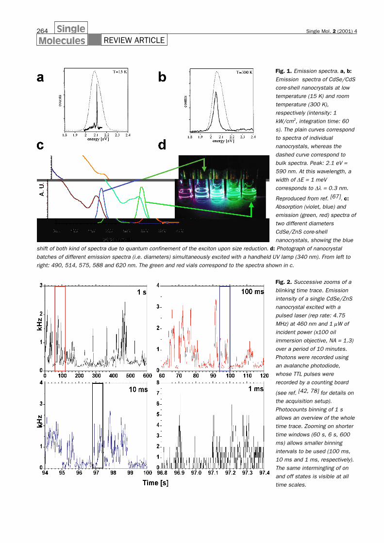
The ensemble emission spectrum of nanocrystals is rathernarrow (30-40 nm) compared to that of standard dyes (seeFig. 1). Also, it is very symmetric, in contrast to conventionaldyes that suffer from a long IR vibronic tail. This widthactually hides the true atomic-like nature of NCs due toinhomogenous broadening. The homogenous linewidth canonly be revealed by single molecule spectroscopy. Atcryogenic temperatures, one observes very narrow individualNC emission spectra (width of a few nm or less), withdistinguishable longitudinal-optical (LO) phonon side-lines(Fig. 1).
264 SingleMolecules REVIEW ARTICLE
Single Mol. 2 (2001) 4
Fig. 1. Emission spectra. a, b:Emission spectra of CdSe/CdS
core-shell nanocrystals at low
temperature (15 K) and room
temperature (300 K),
respectively (intensity: 1
kW/cm2, integration time: 60
s). The plain curves correspond
to spectra of individual
nanocrystals, whereas the
dashed curve correspond to
bulk spectra. Peak: 2.1 eV =
590 nm. At this wavelength, a
width of ∆E = 1 meV
corresponds to ∆λ = 0.3 nm.
Reproduced from ref. [67]. c:Absorption (violet, blue) and
emission (green, red) spectra of
two different diameters
CdSe/ZnS core-shell
nanocrystals, showing the blue
shift of both kind of spectra due to quantum confinement of the exciton upon size reduction. d: Photograph of nanocrystal
batches of different emission spectra (i.e. diameters) simultaneously excited with a handheld UV lamp (340 nm). From left to
right: 490, 514, 575, 588 and 620 nm. The green and red vials correspond to the spectra shown in c.
Fig. 2. Successive zooms of a
blinking time trace. Emission
intensity of a single CdSe/ZnS
nanocrystal excited with a
pulsed laser (rep rate: 4.75
MHz) at 460 nm and 1 µW of
incident power (x100 oil
immersion objective, NA = 1.3)
over a period of 10 minutes.
Photons were recorded using
an avalanche photodiode,
whose TTL pulses were
recorded by a counting board
(see ref. [42, 78] for details onthe acquisition setup).
Photocounts binning of 1 s
allows an overview of the whole
time trace. Zooming on shorter
time windows (60 s, 6 s, 600
ms) allows smaller binning
intervals to be used (100 ms,
10 ms and 1 ms, respectively).
The same intermingling of on
and off states is visible at all
time scales.
265
REVIEW ARTICLEX. Michalet et al.Properties of fluorescent semiconductor nanocrystals
SingleMolecules
The broadening of the ensemble spectrum is partly due tothe size dispersion inherent to the synthesis (inhomogenousbroadening) and partly due to spectral jumps (homogeneousbroadening). By monitoring an individual NC’s spectrum atcryogenic temperatures over several minutes, Empedocleset al discovered shifts of the main peak position rangingfrom a fraction of a nanometer to several nanometers [62],an observation reproduced under 2-photon excitation [63].These spectral jumps are likely due to local changes in theNC’s environment (or for that matter, on its surface),illustrating again its similarity to molecules, for which thesecharacteristics have been documented [64,65]. Gatheringall the recorded emission peaks positions into a histogramrecovered the ensemble spectrum.
An interesting consequence of these jumps is that theline width of each individual QD is integration-timedependent, and somewhat more surprisingly, excitationpower dependent [66], pointing to a photo-excitedmechanism that underlies this phenomenon [67].
Intermittency
More of a surprise, but another illustration of the atomic-likenature of NC is the phenomenon of blinking, first describedby Nirmal et al. [68] and rationalized in terms of Augerionization by Efros and Rosen [69]. This phenomenon isreadily observed with a standard fluorescence microscopelooking with bare eyes at a diluted solution of NCs spreadover a glass coverslip. Individual, bright diffraction-limitedspots alternating between an emitting state ("on” or"bright” state) and a non-emitting state ("off” or "dark”state) can easily be observed. This is a very convenientsignature of single NC, as this behavior is completelycancelled out when an aggregate of several NC is examined(due to simple statistical considerations).
It is worth looking in more detail to the correspondingintensity fluctuations of a single nanocrystal (Fig. 2),recorded with a single-photon counting detector (avalanchephotodiode, APD). The same pattern of on and off timeswas observed, regardless of the integration (observation)time: the on/off structure of the trace is self-similar [70,71]. This phenomenon points to a problem in the definitionof the quantum yield for a single NC, since it is usuallyunderstood that the molecule is in an emitting state [72].The averaged (observed) ensemble quantum yield is in factunderestimating that of the bright periods, due to theircontamination at all time scales by dark periods. Ifembedded in a protect ive polymer layer(polymethylmethacrylate, PMMA), NCs can in fact beobserved without any noticeable sign of bleaching for up tohours (the limiting factors are the thermal drift of the setup -which puts the NC out of focus – and the large data filesgenerated by such acquisitions) ! The same NC can berepeatedly observed over hours, probably emitting billions ofphotons. Some of the NCs may eventually become non-emitting, but since very long off time cannot be excluded,
and some experiments have shown puzzling recovery effects[73], it may still be premature to speak of photobleaching.
On/Off Time Distributions
A statistical analysis of the on and off times at lowtemperature shows two effects: one thermal and onerelated to the excitation intensity [67]. At higher intensity,nanocrystals tend to switch into the off state more often,the averaged off time duration remaining approximatelyindependent of intensity. This can be rationalized by thefollowing Auger ionization model proposed to explain thedark state in nanocrystals [69]: upon each photo-excitation,an electron-hole pair (exciton) is created. In general, it willrecombine and emit a Stokes-shifted photon after a typicallifetime of a few dozens nanoseconds. But at high excitationintensity, there is a chance that another electron-hole pairwill be created. In general, these extra electron-hole pairswill recombine non-radiatively in several tens of picoseconds[74], but sometimes this recombination will eject one of thecarriers of the first pair (say, the electron) by momentumtransfer, which might end up being trapped at a surfacedefect or ejected from the dot (Auger ionization process). Asa result, a lone carrier (here a hole) remains in the dot,causing newly formed electron-hole pairs to non-radiativelyrecombine and leave another lone carrier behind. In somecases, an inverse process can occur either by re-injection ofthe ejected carrier or by a second ionization that effectivelyneutralizes the NC (Auger recombination process). In bothprocesses, an increase in off states occurrences isexpected at higher excitation intensity: i.e. NCs blink moreat higher excitation power.
Interestingly, the distribution of off times is notexponential as would be expected for a thermally controlleddeactivation process [68,75], but instead follows a powerlaw dependence with extremely long off times [70,71].Blinking sets a severe limitation on single NC biologicalexperiments such as tracking and motility assays. It alsohas noticeable effects in more classical microscopyexperiments as shown below.
Correlation Between Spectral Jumps andBlinking
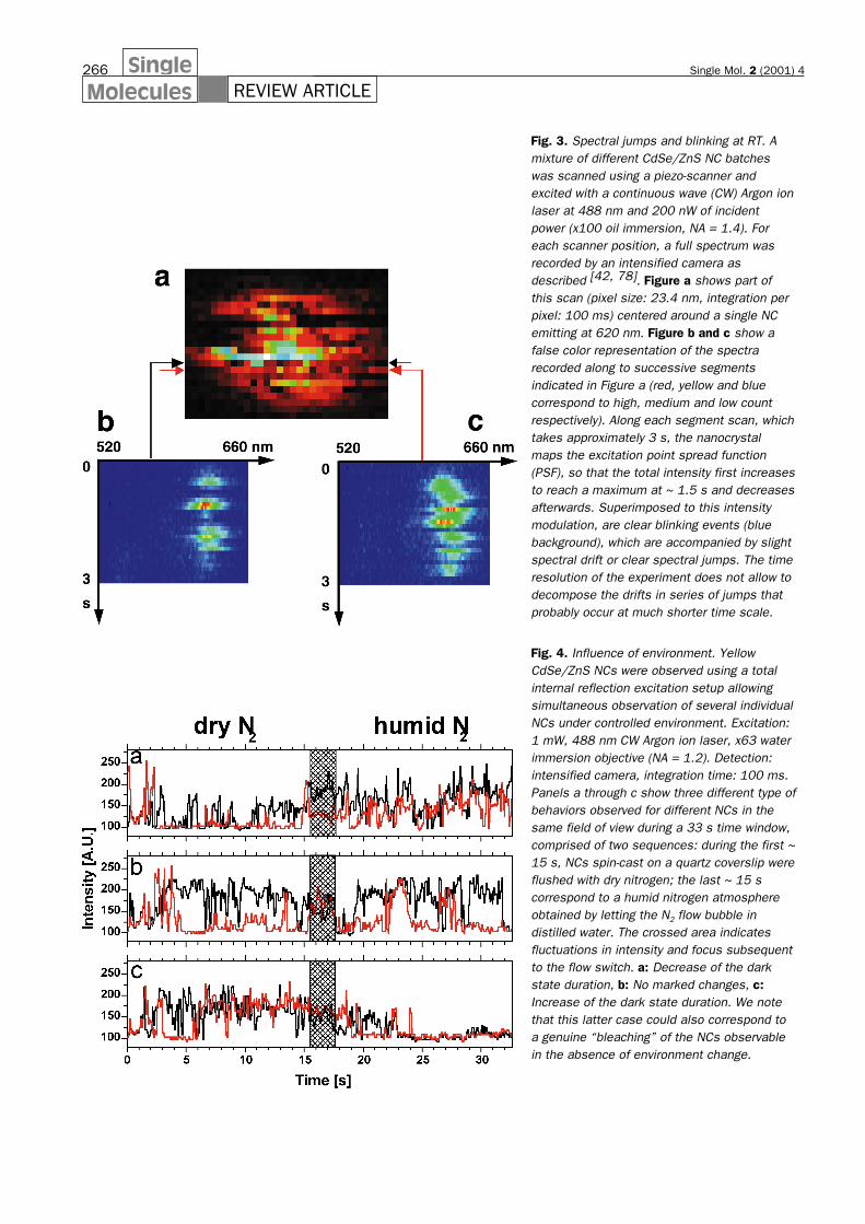
A correlation between spectral jumps and blinking was firstobserved by Neuhauser et al. at low temperature [76]. Thesame phenomenon is observed at room temperature asillustrated in Fig. 3. In Fig. 3a, a sample of spin-coatedsingle nanocrystals was raster-scanned using a custom-made confocal microscope [42]. For each position of thesample, a full emission spectrum is recorded (200 nWincident power (380 W/cm2), 100 ms integration time).
The lines indicated in Fig. 3a are converted to spectraplotted vs. time in Fig. 3b and c: for each pixel in a linescan we obtain a color-coded spectrum that is stackedvertically.
266 SingleMolecules REVIEW ARTICLE
Single Mol. 2 (2001) 4
Fig. 3. Spectral jumps and blinking at RT. Amixture of different CdSe/ZnS NC batcheswas scanned using a piezo-scanner andexcited with a continuous wave (CW) Argon ionlaser at 488 nm and 200 nW of incidentpower (x100 oil immersion, NA = 1.4). Foreach scanner position, a full spectrum wasrecorded by an intensified camera asdescribed [42, 78]. Figure a shows part ofthis scan (pixel size: 23.4 nm, integration perpixel: 100 ms) centered around a single NCemitting at 620 nm. Figure b and c show afalse color representation of the spectrarecorded along to successive segmentsindicated in Figure a (red, yellow and bluecorrespond to high, medium and low countrespectively). Along each segment scan, whichtakes approximately 3 s, the nanocrystalmaps the excitation point spread function(PSF), so that the total intensity first increasesto reach a maximum at ~ 1.5 s and decreasesafterwards. Superimposed to this intensitymodulation, are clear blinking events (bluebackground), which are accompanied by slightspectral drift or clear spectral jumps. The timeresolution of the experiment does not allow todecompose the drifts in series of jumps thatprobably occur at much shorter time scale.
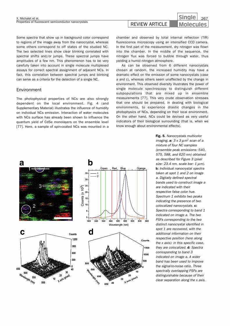
Fig. 4. Influence of environment. YellowCdSe/ZnS NCs were observed using a totalinternal reflection excitation setup allowingsimultaneous observation of several individualNCs under controlled environment. Excitation:1 mW, 488 nm CW Argon ion laser, x63 waterimmersion objective (NA = 1.2). Detection:intensified camera, integration time: 100 ms.Panels a through c show three different type ofbehaviors observed for different NCs in thesame field of view during a 33 s time window,comprised of two sequences: during the first ~15 s, NCs spin-cast on a quartz coverslip wereflushed with dry nitrogen; the last ~ 15 scorrespond to a humid nitrogen atmosphereobtained by letting the N2 flow bubble indistilled water. The crossed area indicatesfluctuations in intensity and focus subsequentto the flow switch. a: Decrease of the darkstate duration, b: No marked changes, c:Increase of the dark state duration. We notethat this latter case could also correspond toa genuine “bleaching” of the NCs observablein the absence of environment change.
267
REVIEW ARTICLEX. Michalet et al.Properties of fluorescent semiconductor nanocrystals
SingleMolecules
Some spectra that show up in background color correspondto regions of the image away from the nanocrystal, whereassome others correspond to off states of the studied NC.The two selected lines show clear blinking correlated withspectral shifts and/or jumps. These spectral jumps haveamplitudes of a few nm. This phenomenon has to be verycarefully taken into account in single molecule multiplexedassays for correct spectral assignment of adjacent NCs. Infact, this correlation between spectral jumps and blinkingcan serve as a criteria for the detection of a single NC.
Environment
The photophysical properties of NCs are also stronglydependent on the local environment. Fig. 4 (andSupplementary Material) illustrates the influence of humidityon individual NCs emission. Interaction of water moleculeswith NCs surface has already been shown to influence thequantum yield of CdSe monolayers on the ensemble level[77]. Here, a sample of spin-coated NCs was mounted in a
chamber and observed by total internal reflection (TIR)fluorescence microscopy using an intensified CCD camera.In the first part of the measurement, dry nitrogen was flowninto the chamber. In the middle of the sequence, thenitrogen flux was forced to bubble through water, thusyielding a humid nitrogen atmosphere.
As can be observed from 6 different nanocrystalschosen at random, the increased humidity may have adramatic effect on the emission of some nanocrystals (casea and c), whereas others seem unaffected by the change inenvironment. This observed diversity illustrates the power ofsingle molecule spectroscopy to distinguish differentsubpopulations that are mixed up in ensemblemeasurements [77]. This very crude observation stressesthat one should be prepared, in dealing with biologicalenvironments, to experience drastic changes in thephotophysics of NCs, depending on their local environment.On the other hand, NCs could be devised as very usefulindicators of their biological surrounding (that is, when weknow enough about environmental effects).
Fig. 5. Nanocrystals multicolorimaging. a: 3 x 3 µm2 scan of amixture of four NC samples(ensemble peak emissions: 540,575, 588, and 620 nm) obtainedas described for Figure 3 (pixelsize: 23.4 nm, scale bar: 1 µm).b: Individual nanocrystal spectrataken at spot 1 and 2 on imagea. Digitally defined spectralbands used to construct image aare indicated with theirrespective false color hue.Spectrum 1 exhibits two peaksindicating the presence of twocolocalized nanocrystals. c:Spectra corresponding to band 1indicated on image a. The twoPSFs corresponding to the twodistinct nanocrystal identified inspot 1 are recovered, with theadditional information on theirrespective position (here alongthe x axis): in this specific case,they are colocalized. d: Spectracorresponding to band 3indicated on image a. A widerband has been used to improvethe signal-to-noise ratio. Threespectrally overlapping PSFs aredistinguishable because of theirclear separation along the x axis.
268 SingleMolecules REVIEW ARTICLE
Single Mol. 2 (2001) 4
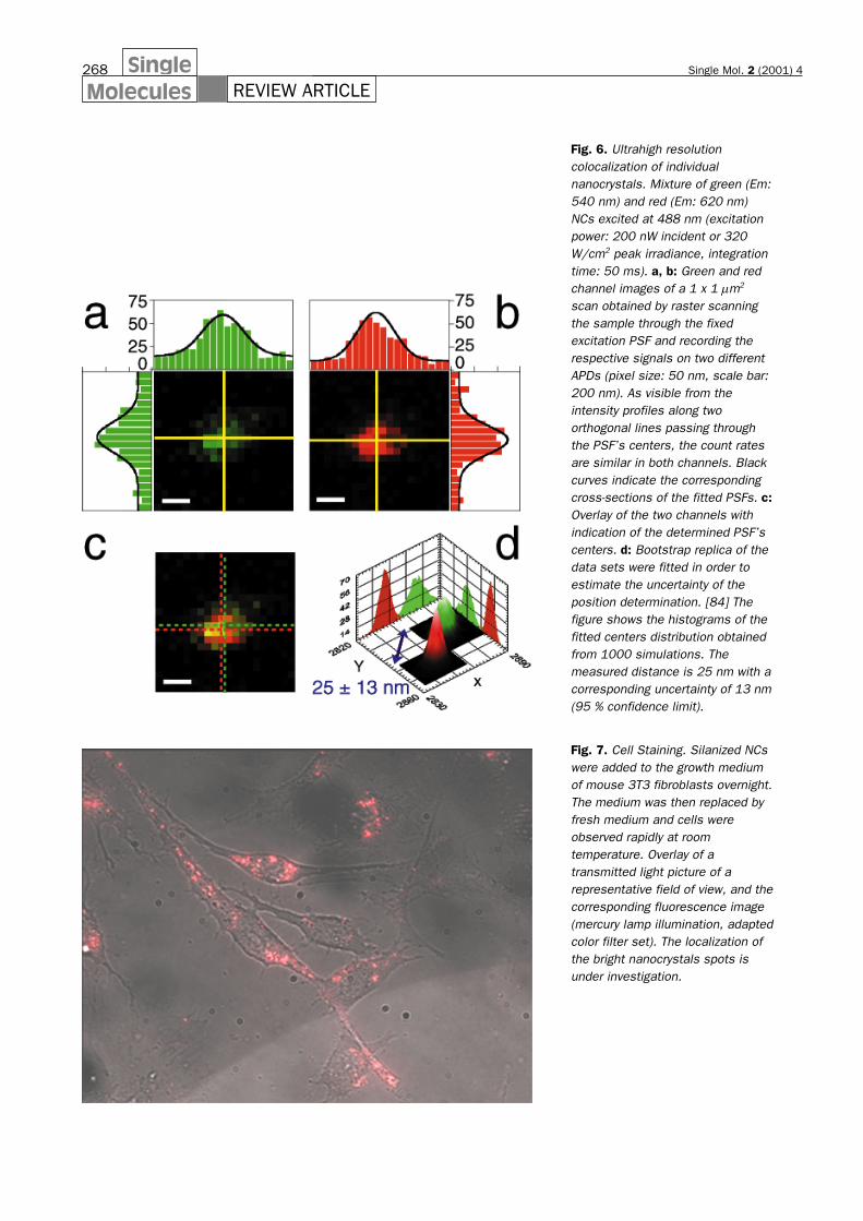
Fig. 6. Ultrahigh resolutioncolocalization of individualnanocrystals. Mixture of green (Em:540 nm) and red (Em: 620 nm)NCs excited at 488 nm (excitationpower: 200 nW incident or 320W/cm2 peak irradiance, integrationtime: 50 ms). a, b: Green and redchannel images of a 1 x 1 µm2
scan obtained by raster scanningthe sample through the fixedexcitation PSF and recording therespective signals on two differentAPDs (pixel size: 50 nm, scale bar:200 nm). As visible from theintensity profiles along twoorthogonal lines passing throughthe PSF’s centers, the count ratesare similar in both channels. Blackcurves indicate the correspondingcross-sections of the fitted PSFs. c:Overlay of the two channels withindication of the determined PSF’scenters. d: Bootstrap replica of thedata sets were fitted in order toestimate the uncertainty of theposition determination. [84] Thefigure shows the histograms of thefitted centers distribution obtainedfrom 1000 simulations. Themeasured distance is 25 nm with acorresponding uncertainty of 13 nm(95 % confidence limit).
Fig. 7. Cell Staining. Silanized NCswere added to the growth mediumof mouse 3T3 fibroblasts overnight.The medium was then replaced byfresh medium and cells wereobserved rapidly at roomtemperature. Overlay of atransmitted light picture of arepresentative field of view, and thecorresponding fluorescence image(mercury lamp illumination, adaptedcolor filter set). The localization ofthe bright nanocrystals spots isunder investigation.

269
REVIEW ARTICLEX. Michalet et al.Properties of fluorescent semiconductor nanocrystals
SingleMolecules
Taking Advantage of NCs Properties:Multicolor Imaging and Ultrahigh-resolution Colocalization
The properties of NCs can be exploited in unique ways.Below we review several novel methodologies that weredeveloped in our lab.
A detailed description of the custom-made microscopesused in these studies is given elsewhere [42, 78, 79].
A single excitation line is sufficient to excite differentNCs above their band edge and have them all emit at theirrespective wavelengths. This has the obvious advantagethat one does not have different chromatic aberrations inthe optics of the excitation path, nor does one have to aligndifferent excitation beams. We use a stage-scanningconfocal set-up with the excitation beam fixed on the opticalaxis. Nanometer-accuracy positioning is provided by aclosed-loop piezo-scanner. An oil-immersion, high NAobjective serves both for excitation and collection of theemitted light (epi-illumination).
The simplest detection path we use is composed of twosingle-photon counting APDs. The signals are spectrallyseparated using dichroic mirrors and emission filters. Whilescanning, two separate data sets are recordedsimultaneously, and since they result from emission fromthe same exact point in the sample, they are in perfectregistry. The advantage of this configuration is a very highsensitivity and time resolution (in the ns range).
A second type of detection is selected when the numberof spectral channels to be monitored is larger than two. Thisis done by flipping a mirror and redirecting the collectedphotons to a different path. It would indeed be quiteinconvenient to separate multiple colors with multipledichroic mirrors and detect them with multiple APDs.Instead, the detected photons are dispersed with aBrewster angle prism and imaged onto the photocathode ofan intensified CCD camera. The resulting data set consistsof a series of spectra, one for each scanned pixel. Thetemporal resolution of this system is limited to 1 ms, butthe noise level and the reduced signal due to the spectraldispersion set a practical limitation of about 50 ms for NCimaging.
Nanocrystal Multicolor Imaging
The narrow emission of NCs permits the preparation ofmixture of several NC batches with distinct ensemblespectra. It seems natural to look at the recorded data usingour prior knowledge of these ensemble spectra and todefine spectral bands that correspond to each individualbatch. However, due to overlaps between the ensemblespectra at their tails and due to spectral differences fromone NC to another, this approach leads to images that aredifficult to interpret.
These problems are illustrated in Fig. 5e digitally definedspectral bands. However, if we go back to the correspondingspectra (Fig. 5b), they correspond to two differentsituations. In case 1, two distinct spectra are present, eachfitting nicely in one predefined spectral band. The multicoloraspect of the spot truly corresponds to different colocalizedNCs. On the other hand, case 2 corresponds to a single NCwith its spectrum overlapping two spectral bands.If instead of analyzing the data by predefined bands weutilize the full X-Y-λ data space (or at least at a projection ofthis space onto the X-λ plane), it is easy to separate NCsthat are indistinguishable spatially (they are colocalized),but well separated spectrally (Fig. 5c, case 1); equally well,it is possible to separate NCs that have similar spectra butare well separated in space (> Rayleigh criterion) (Fig. 5d,case 3). Of course in this process, we are ignoring onespatial dimension (Y), which may lift the observeddegeneracy in the other dimensions. In conclusion, to fullytake advantage of the spectral variety of nanocrystals, somenew representation and analysis tools are needed, that gobeyond the traditional definition of fixed spectral bands[80].
Nanometer-Resolution MulticolorColocalization
Another very powerful use of NCs in fluorescencemicroscopy is taking advantage of their broad excitationspectrum to improve the resolution of distancemeasurements. Let’s consider two spectrally separatednanocrystal batches, spin-coated on a coverslip andobserved with the dual channel detection path. The perfectregistration of the two channels allows finding out theprecise position of each object in the object plane, by fittingthe theoretical excitation spot to the observed image [81-83].
It can be shown theoretically, and verified numerically,that for large enough signal-to-noise ratio, and for largeenough number of pixels, subpixel accuracy in X and Y canbe achieved [81]. In fact, the 2-dimensional fit is even moreefficient that a 1-dimensional fit, because there is only oneextra parameter (the extra center coordinate), while thenumber of data points is squared [78]. A crucial ingredientis that the position and size of each pixel be preciselyknown, achievable with a nm-resolution closed-loop piezoscanner.
As an illustration, Fig. 6 shows a scan of randomlydispersed nanocrystals, observed in conditions were theyexhibited moderate blinking. A fit of the respective positionsof the overlapping spots gives a distance of approximately25 nm [42]. The uncertainty in this distance measurementwas calculated using the bootstrap method [84]. It yielded afinal distance of 25 nm and a "2σ” error bar of 13 nm,comparable to the error bar obtained for non-blinking beads
270 SingleMolecules REVIEW ARTICLE
Single Mol. 2 (2001) 4
[42, 79]. Strong blinking significantly affects the reliability ofthe fit, and a careful analysis of the validity of the bootstrapestimation has in principle to be performed for each blinkingstatistics. Assuming a power law distribution, it can beshown that the error bar remains reasonably small, eventhough it is not as good as in the non-blinking case. In anycase, the calculated error bar is of the order of the NCs’size, and is therefore close to the best achievableresolution.
Some Examples of Biological Applications
of NCs
We now review a few examples of actual use of NCs in a
biological context. As a matter of fact, this is a burgeoning
field, so that many applications like cell sorting [57],
immunoassays [39,40] or fluorescence in situ hybridization
[85] among many others [86] will only be evoked here. In
addition, we will focus on silanized nanocrystals. Not many
of these applications attain the single molecule sensitivity
level at this point, but there is no fundamental obstacle to
reach this goal in the near future.
Intracellular Staining
The simplest application we can think of is to use thesebright fluorescent probes to illuminate the interior of cells.Live cells staining using organic dyes is a well establishedtechnique, but unless the cells are loaded with largeamount of dye molecules, the stain will eventually bleachdue to photophysical degradation. As we have seen,individual NCs have high quantum yields and can emit avery large number of photons, such that a smaller numberof probes should be needed to get similar results, reducingthe risk of toxicity for the cell. Several methods can be usedto load cells with silanized NCs, but certainly the mostsimple one simply consists of incubating the cells in amedium containing NCs and replacing the medium after awhile to wash out the non-incorporated NCs. Surprisingly,this works rather well for 3T3 fibroblasts (see Fig. 7), mostlikely due to endocytosis of the NCs. In this process, localinvaginations of the cell membrane encompass adsorbedNCs into vesicles, which possibly release their cargo in thelysosomes. The exact pathways involved in this uptakeprocess are under investigation.
This proof of principle experiment shows that cells cansurvive a diet of nanocrystals. Some yeast strains andbacteria do actually much better and synthesize CdSnanocrystals by themselves when placed in a Cd-richmedium [87,88] in an attempt to detoxify their growthmedium. The resulting CdS nanocrystals exhibit the same
quantum confinement properties as synthetic ones, buttend to degrade upon photoexcitation [89-92].
Functionalization
The next step in cell biology is to target NCs to specificcompartments, organelles or molecules. A classicalexample of these affinity pairs is the biotin-streptavidin pair.Biotin (vitamin) is a small molecule, whereas streptavidin isa 60 kDa protein that can afford to bind up to 4 biotins.Taking advantage of either the NH2 or SH groups left byamino-propyl silane or mercapto-propyl silane on the surfaceof silanized NCs, it is possible to use commercially availablereactive biotin molecules and covalently attach them on thesurface of NCs [57]. The efficiency of biotinylation can bechecked by gel shift assay, whereby the migration of asample of free biotinylated NCs under electric field iscompared to that of the same sample mixed with increasingquantities of streptavidin. Whereas singly biotinylated NCsmigrate up to a certain point as a relatively narrow band,this band slows down upon addition of streptavidin, which isa signature of the probe’s activity (attachment tostreptavidin). If more biotins are attached onto each NCduring functionalization, one expects that either severalstreptavidin will bind to each single NC, or that a singlestreptavidin may cross-link two biotinylated NCs, slowingdown even further the migration of the band in the gel. Theexperiments fully confirm this picture and similar strategiescan be used to attach nanocrystals to antibodies or othermolecules, and the same sort of test is used todemonstrate specificity.
Fixed Cell Labelling
The first example of specific labeling was obtained earlyusing this simple strategy of biotin functionalization of NCsas illustrated in Fig. 8 [37]. Using cells that were fixed(essentially plasticized) and incubated with biotinylatedphalloidin that binds to F-actin filaments, the cytoskeletonwas decorated with biotins. Then streptavidin was added,and bound to the biotins present on the filaments. The nextstep consisted, after rinsing off all the unattachedstreptavidins, in incubation with the biotinylated NCs, whichbound to one of the 3 remaining binding sites of thestreptavidins. This type of "sandwich” labeling scheme wasrepeated once to increase the signal’s brightness. Apositively charged species of green NCs was added andturned out to bind preferentially within the nucleus. Thiscolorful picture is nothing extraordinary for cell biologistswho are used to multicolor, specific staining of differentorganelles or molecules with organic dyes, but it was anencouraging step towards more ambitious goals. Inparticular, it was taken using a single excitation source forboth colors simultaneously.
271
REVIEW ARTICLEX. Michalet et al.Properties of fluorescent semiconductor nanocrystals
SingleMolecules
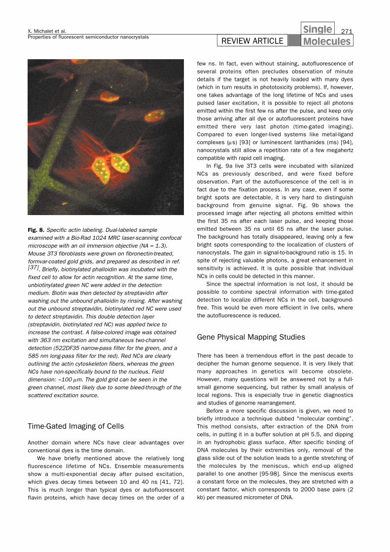
Fig. 8. Specific actin labeling. Dual-labeled sampleexamined with a Bio-Rad 1024 MRC laser-scanning confocalmicroscope with an oil immersion objective (NA = 1.3).Mouse 3T3 fibroblasts were grown on fibronectin-treated,formvar-coated gold grids, and prepared as described in ref.[37]. Briefly, biotinylated phalloidin was incubated with thefixed cell to allow for actin recognition. At the same time,unbiotinylated green NC were added in the detectionmedium. Biotin was then detected by streptavidin afterwashing out the unbound phalloidin by rinsing. After washingout the unbound streptavidin, biotinylated red NC were usedto detect streptavidin. This double detection layer(streptavidin, biotinylated red NC) was applied twice toincrease the contrast. A false-colored image was obtainedwith 363 nm excitation and simultaneous two-channeldetection (522DF35 narrow-pass filter for the green, and a585 nm long-pass filter for the red). Red NCs are clearlyoutlining the actin cytoskeleton fibers, whereas the greenNCs have non-specifically bound to the nucleus. Fielddimension: ~100 µm. The gold grid can be seen in thegreen channel, most likely due to some bleed-through of thescattered excitation source.
Time-Gated Imaging of Cells
Another domain where NCs have clear advantages overconventional dyes is the time domain.
We have briefly mentioned above the relatively longfluorescence lifetime of NCs. Ensemble measurementsshow a multi-exponential decay after pulsed excitation,which gives decay times between 10 and 40 ns [41, 72].This is much longer than typical dyes or autofluorescentflavin proteins, which have decay times on the order of a
few ns. In fact, even without staining, autofluorescence ofseveral proteins often precludes observation of minutedetails if the target is not heavily loaded with many dyes(which in turn results in phototoxicity problems). If, however,one takes advantage of the long lifetime of NCs and usespulsed laser excitation, it is possible to reject all photonsemitted within the first few ns after the pulse, and keep onlythose arriving after all dye or autofluorescent proteins haveemitted there very last photon (time-gated imaging).Compared to even longer-lived systems like metal-ligandcomplexes (µs) [93] or luminescent lanthanides (ms) [94],nanocrystals still allow a repetition rate of a few megahertzcompatible with rapid cell imaging.
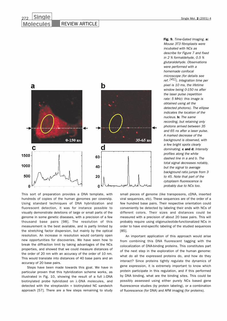
In Fig. 9a live 3T3 cells were incubated with silanizedNCs as previously described, and were fixed beforeobservation. Part of the autofluorescence of the cell is infact due to the fixation process. In any case, even if somebright spots are detectable, it is very hard to distinguishbackground from genuine signal. Fig. 9b shows theprocessed image after rejecting all photons emitted withinthe first 35 ns after each laser pulse, and keeping thoseemitted between 35 ns until 65 ns after the laser pulse.The background has totally disappeared, leaving only a fewbright spots corresponding to the localization of clusters ofnanocrystals. The gain in signal-to-background ratio is 15. Inspite of rejecting valuable photons, a great enhancement insensitivity is achieved. It is quite possible that individualNCs in cells could be detected in this manner.
Since the spectral information is not lost, it should bepossible to combine spectral information with time-gateddetection to localize different NCs in the cell, background-free. This would be even more efficient in live cells, wherethe autofluorescence is reduced.
Gene Physical Mapping Studies
There has been a tremendous effort in the past decade todecipher the human genome sequence. It is very likely thatmany approaches in genetics will become obsolete.However, many questions will be answered not by a full-small genome sequencing, but rather by small analysis oflocal regions. This is especially true in genetic diagnosticsand studies of genome rearrangement.
Before a more specific discussion is given, we need tobriefly introduce a technique dubbed "molecular combing”.This method consists, after extraction of the DNA fromcells, in putting it in a buffer solution at pH 5.5, and dippingin an hydrophobic glass surface. After specific binding ofDNA molecules by their extremities only, removal of theglass slide out of the solution leads to a gentle stretching ofthe molecules by the meniscus, which end-up alignedparallel to one another [95-98]. Since the meniscus exertsa constant force on the molecules, they are stretched with aconstant factor, which corresponds to 2000 base pairs (2kb) per measured micrometer of DNA.
272 SingleMolecules REVIEW ARTICLE
Single Mol. 2 (2001) 4
Fig. 9. Time-Gated Imaging. a:Mouse 3T3 fibroplasts wereincubated with NCs asdescribe for Figure 7 and fixedin 2 % formaldehyde, 0.5 %glutaraldehyde. Observationswere performed with ahomemade confocalmicroscope (for details seeref. [41]). Integration time perpixel is 10 ms, the lifetimewindow being 0-150 ns afterthe laser pulse (repetitionrate: 5 MHz): this image isobtained using all thedetected photons). The ellipseindicates the location of thenucleus. b: The samerecording, but retaining onlyphotons arrived between 35and 65 ns after a laser pulse.A marked decrease of thebackground is observed, witha few bright spots clearlydominating. c and d: Intensityprofiles along the whitedashed line in a and b. Thet ot al s i g n al de c r ea s es notably,but the signal to a v e r a g e b ac k g r o u nd r a t i o j um ps from 3to 45. Note that part of thecytoplasm fluorescence isprobably due to NCs too.
This sort of preparation provides a DNA template, withhundreds of copies of the human genomes per coverslip.Using standard techniques of DNA hybridization andfluorescent detection, it was for instance possible tovisually demonstrate deletions of large or small parts of thegenome in some genetic diseases, with a precision of a fewthousand base pairs [98]. The resolution of thismeasurement is the best available, and is partly limited bythe stretching factor dispersion, but mainly by the opticalresolution. An increase in resolution would certainly opennew opportunities for discoveries. We have seen how tobreak the diffraction limit by taking advantages of the NCsproperties, and showed that we could measure distances ofthe order of 20 nm with an accuracy of the order of 10 nm.This would translate into distances of 40 base pairs and anaccuracy of 20 base pairs.
Steps have been made towards this goal. We have inparticular proven that this hybridization scheme works, asillustrated in Fig. 10, showing the result of a full λ-DNAbiotinylated probe hybridized on λ -DNA molecules, anddetected with the streptavidin + biotinylated NC sandwichapproach [57]. There are a few steps remaining to study
small pieces of genome (like transposons, cDNA, insertedviral sequences, etc). These sequences are of the order of afew hundred base pairs. Their respective orientation couldconveniently be detected by labeling their ends with NCs ofdifferent colors. Their sizes and distances could bemeasured with a precision of about 20 base pairs. This willprobably require using oligonucleotide-functionalized NCs inorder to have end-specific labeling of the studied sequences[85].
An important application of this approach would arise
from combining this DNA fluorescent tagging with the
colocalization of DNA-binding proteins. This constitutes part
of the next step in the exploration of the human genome:
what do all the expressed proteins do, and how do they
interact? Since proteins tightly regulate the dynamics of
gene expression, it is extremely important to know which
protein participate in this regulation, and if this performed
by DNA binding, what are the binding sites. This could be
possibly assessed using either purely NCs based gene
fluorescence studies (by protein labeling), or a combinationof fluorescence (for DNA) and AFM imaging (for proteins).
273
REVIEW ARTICLEX. Michalet et al.Properties of fluorescent semiconductor nanocrystals
SingleMolecules
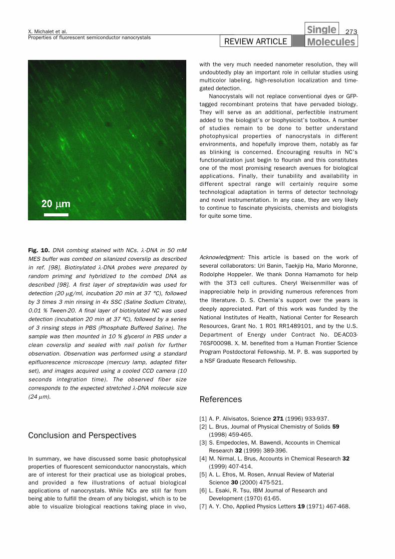
Fig. 10. DNA combing stained with NCs. λ-DNA in 50 mM
MES buffer was combed on silanized coverslip as described
in ref. [98]. Biotinylated λ-DNA probes were prepared by
random priming and hybridized to the combed DNA as
described [98]. A first layer of streptavidin was used for
detection (20 µg/ml, incubation 20 min at 37 °C), followed
by 3 times 3 min rinsing in 4x SSC (Saline Sodium Citrate),
0.01 % Tween-20. A final layer of biotinylated NC was used
detection (incubation 20 min at 37 ºC), followed by a series
of 3 rinsing steps in PBS (Phosphate Buffered Saline). The
sample was then mounted in 10 % glycerol in PBS under a
clean coverslip and sealed with nail polish for further
observation. Observation was performed using a standard
epifluorescence microscope (mercury lamp, adapted filter
set), and images acquired using a cooled CCD camera (10
seconds integration time). The observed fiber size
corresponds to the expected stretched λ-DNA molecule size
(24 µm).
Conclusion and Perspectives
In summary, we have discussed some basic photophysicalproperties of fluorescent semiconductor nanocrystals, whichare of interest for their practical use as biological probes,and provided a few illustrations of actual biologicalapplications of nanocrystals. While NCs are still far frombeing able to fulfill the dream of any biologist, which is to beable to visualize biological reactions taking place in vivo,
with the very much needed nanometer resolution, they willundoubtedly play an important role in cellular studies usingmulticolor labeling, high-resolution localization and time-gated detection.
Nanocrystals will not replace conventional dyes or GFP-tagged recombinant proteins that have pervaded biology.They will serve as an additional, perfectible instrumentadded to the biologist’s or biophysicist’s toolbox. A numberof studies remain to be done to better understandphotophysical properties of nanocrystals in differentenvironments, and hopefully improve them, notably as faras blinking is concerned. Encouraging results in NC’sfunctionalization just begin to flourish and this constitutesone of the most promising research avenues for biologicalapplications. Finally, their tunability and availability indifferent spectral range will certainly require sometechnological adaptation in terms of detector technologyand novel instrumentation. In any case, they are very likelyto continue to fascinate physicists, chemists and biologistsfor quite some time.
Acknowledgment: This article is based on the work ofseveral collaborators: Uri Banin, Taekjip Ha, Mario Moronne,
Rodolphe Hoppeler. We thank Donna Hamamoto for help
with the 3T3 cell cultures. Cheryl Weisenmiller was of
inappreciable help in providing numerous references from
the literature. D. S. Chemla’s support over the years is
deeply appreciated. Part of this work was funded by the
National Institutes of Health, National Center for Research
Resources, Grant No. 1 R01 RR1489101, and by the U.S.
Department of Energy under Contract No. DE-AC03-
76SF00098. X. M. benefited from a Human Frontier Science
Program Postdoctoral Fellowship. M. P. B. was supported by
a NSF Graduate Research Fellowship.
References
[1] A. P. Alivisatos, Science 271 (1996) 933-937.[2] L. Brus, Journal of Physical Chemistry of Solids 59
(1998) 459-465.[3] S. Empedocles, M. Bawendi, Accounts in Chemical
Research 32 (1999) 389-396.[4] M. Nirmal, L. Brus, Accounts in Chemical Research 32
(1999) 407-414.[5] A. L. Efros, M. Rosen, Annual Review of Material
Science 30 (2000) 475-521.[6] L. Esaki, R. Tsu, IBM Journal of Research and
Development (1970) 61-65.[7] A. Y. Cho, Applied Physics Letters 19 (1971) 467-468.
274 SingleMolecules REVIEW ARTICLE
Single Mol. 2 (2001) 4
[8] R. Dingle, A. C. Gossard, H. L. Stormer, BellLaboratories Record 58 (1980) 274-281.
[9] A. C. Gossard, IEEE Journal of Quantum Electronics QE-22 (1986) 1649-1655.
[10] L. Esaki, IEEE Journal of Quantum Electronics QE-22(1986) 1611-1624.
[11] Y. Arakawa, H. Sakaki, Applied Physics Letters 40(1982) 939-941.
[12] R. Dingle, W. Wiegmann, C. H. Henry, Physical ReviewLetters 33 (1974) 827-830.
[13] R. C. Miller, D. A. Kleinman, W. T. Tsang, A. C.Gossard, Physical Review B 24 (1981) 1134-1136.
[14] P. M. Petroff, A. C. Gossard, R. A. Logan, W.Wiegmann, Applied Physics Letters 41 (1982) 635-638.
[15] Y. Arakawa, A. Yariv, IEEE Journal of QuantumElectronics QE-22 (1986) 1887-1899.
[16] M. Asada, Y. Miyamoto, Y. Suematsu, IEEE Journal ofQuantum Electronics QE-22 (1986) 1915-1921.
[17] A. I. Ekimov, A. A. Onuschenko, Sov. Phys. Semicond.16 (1982) 775-778.
[18] A. L. Efros, A. L. Efros, Sov. Phys. Semicond. 16(1982) 772-775.
[19] D. Duonghong, J. Ramsden, M. Grätzel, Journal of theAmerican Chemical Society 104 (1982) 2985-2988.
[20] A. Henglein, Journal of Physical Chemistry 86 (1982)2291-2293.
[21] J. Kuczynski, J. K. Thomas, Chemical Physics Letters88 (1982) 445-447.
[22] R. Rossetti, L. Brus, Journal of Physical Chemistry 86(1982) 4470-4472.
[23] G. Hodes, J. Manassen, D. Cahen, Nature 261 (1976)403-404.
[24] B. Miller, A. Heller, Nature 262 (1976) 680-681.
[25] L. E. Brus, Journal of Chemical Physics 79 (1983)5566-5571.
[26] A. Fotjik, H. Weller, U. Koch, A. Henglein, Ber.Bunsenges. Phys. Chem. 88 (1984) 969-977.
[27] M. L. Steigerwald, A. P. Alivisatos, J. M. Gibson, T. D.Harris, R. Kortan, A. J. Muller, A. M. Thayer, T. M.Duncan, D. C. Douglass, L. E. Brus, Journal of theAmerican Chemical Society 110 (1988) 3046-3050.
[28] A. R. Kortan, R. Hull, R. L. Opila, M. G. Bawendi, M. L.Steigerwald, P. J. Carroll, L. E. Brus, Journal of theAmerican Chemical Society 112 (1990) 1327-1332.
[29] C. B. Murray, D. J. Norris, M. G. Bawendi, Jounal of theAmerican Chemical Society 115 (1993) 8706-8715.
[30] X. Peng, J. Wickham, A. P. Alivisatos, Journal of theAmerican Chemical Society 120 (1998) 5343-5344.
[31] L. Manna, E. C. Scher, A. P. Alivisatos, Journal of theAmerican Chemical Society 122 (2000) 12700-12706.
[32] A. Eychmüller, A. Mews, H. Weller, Chemical PhysicsLetters 208 (1993) 59-62.
[33] A. Mews, A. Eychmüller, M. Giersig, D. Schoos, H.Weller, Journal of Physical Chemistry 98 (1994) 934-941.
[34] M. A. Hines, P. Guyot-Sionnest, Journal of PhysicalChemistry 100 (1996) 468-471.
[35] R. O. Dabbousi, J. Rodriguez-Viejo, F. V. Mikulec, J. R.Heine, H. Mattoussi, R. Ober, K. F. Jensen, M. G.Bawendi, Journal of Physical Chemistry B 101 (1997)9463-9475.
[36] X. Peng, M. C. Schlamp, A. V. Kadavanich, A. P.Alivisatos, Journal of the American Chemical Society119 (1997) 7019-7029.
[37] M. Bruchez, M. Moronne, P. Gin, S. Weiss, A. P.Alivisatos, Science 281 (1998) 2013-2015.
[38] W. C. W. Chan, S. Nie, Science 281 (1998) 2016-2018.
[39] H. Mattoussi, J. M. Mauro, E. R. Goldman, G. P.Anderson, V. C. Sundar, F. V. Mikulec, M. G. Bawendi,Journal of the American Chemical Society 122 (2000)12142-12250.
[40] B. Sun, W. Xie, G. Yi, D. Chen, Y. Zhou, J. Cheng,Journal of Immunological Methods 249 (2001) 85-89.
[41] M. Dahan, T. Laurence, F. Pinaud, D. S. Chemla, A. P.Alivisatos, M. Sauer, S. Weiss, Optics Letters 26(2001) 825-827.
[42] T. D. Lacoste, X. Michalet, F. Pinaud, D. S. Chemla, A.P. Alivisatos, S. Weiss, Proceedings of the NationalAcademy of Sciences USA 97 (2000) 9461–9466.
[43] V. I. Klimov, A. A. Mikhailovsky, S. Xu, A. Malko, J. A.Hollingsworth, C. A. Leatherdale, H.-J. Eisler, M. G.Bawendi, Science 290 (2000) 314-317.
[44] B. O. Dabbousi, M. G. Bawendi, O. Onitsuka, M. F.Rubner, Applied Physics Letters 66 (1995) 1316-1318.
[45] V. Colvin, M. Schlamp, A. P. Alivisatos, Nature 370(1994) 354-357.
[46] C. Wang, M. Shim, P. Guyot-Sionnest, Science 291(2001) 2390-2392.
[47] H. Weller, U. Koch, M. Gutiérrez, A. Henglein, Berichteder Bunsengesellschaft Physical Chemistry 88 (1984)649-656.
[48] M. A. Hines, P. Guyot-Sionnest, Journal of PhysicalChemisry B 102 (1998) 3655-3657.
[49] A. Mews, A. Eychmûller, Berichte der
Bunsengesellschaft. Physical Chemistry 102 (1998)
1343-1357.
[50] A. A. Guzelian, J. E. B. Katari, A. V. Kadavanich, U.
Banin, K. Hamad, E. Juban, A. P. Alivisatos, R. H.
Wolters, C. C. Arnold, J. R. Heath, Journal of Physical
Chemistry 100 (1996) 7212-7219.
[51] A. A. Guzelian, U. Banin, A. V. Kadavanich, X. Peng, A.
P. Alivisatos, Applied Physics Letters 69 (1996) 1432-
1434.

275
REVIEW ARTICLEX. Michalet et al.Properties of fluorescent semiconductor nanocrystals
SingleMolecules
[52] J. E. B. Bowen Katari, V. L. Colvin, A. P. Alivisatos,Journal of Physical Chemistry 98 (1994) 4109-4117.
[53] Z. A. Peng, X. Peng, Journal of the American ChemicalSociety 123 (2001) 183-184.
[54] L. Qu, A. Peng, X. Peng, Nanoletters 1 (2001) 333-337.
[55] A. Kadavanich, V., T. C. Kippeny, M. M. Erwin, S. J.Pennycook, S. J. Rosenthal, Journal of PhysicalChemistry B 105 (2001) 361-369.
[56] K. W. Böer, Survey of Semiconductor Physics.Electrons and Other Particles in Bulk Semiconductors,Van Nostrand Reinhold, New York 1990.
[57] M. Bruchez, PhD Thesis, Department of Chemistry, UCBerkeley, Berkeley 1998.
[58] D. Gerion, F. Pinaud, S. C. Williams, W. J. Parak, D.Zanchet, S. Weiss, A. P. Alivisatos, Journal of PhysicalChemistry B (2001) 8861-8871.
[59] M. A. Correa-Duarte, M. Giersig, L. M. Liz-Marzán,Chemical Physics Letters 286 (1998) 497-501.
[60] C. C. Chen, C. P. Yet, H. N. Wang, C. Y. Chao,Langmuir 15 (1999) 6845.
[61] G. P. Mitchell, C. A. Mirkin, R. L. Letsinger, Journal ofthe American Chemical Society 121 (1999) 8122-8123.
[62] S. A. Empedocles, D. J. Norris, M. G. Bawendi,Physical Review Letters 77 (1996) 3873-3876.
[63] S. A. Blanton, M. A. Hines, P. Guyot-Sionnest, AppliedPhysics Letters 69 (1996) 3905-3907.
[64] M. Orrit, J. Bernard, Physical Review Letters 65 (1990)2716-2719.
[65] W. P. Ambrose, W. E. Moerner, Nature 349 (1991)225-227.
[66] S. A. Empedocles, M. G. Bawendi, Journal of PhysicalChemistry 103 (1999) 1826-1830.
[67] U. Banin, M. Bruchez, A. P. Alivisatos, T. Ha, S. Weiss,D. S. Chemla, Journal of Chemical Physics 110 (1999)1195-1201.
[68] M. Nirmal, B. O. Dabbousi, M. G. Bawendi, J. J.Macklin, J. K. Trautman, T. D. Harris, L. E. Brus, Nature383 (1996) 802-804.
[69] A. L. Efros, M. Rosen, Physical Review Letters 78(1997) 1110-1113.
[70] M. Kuno, D. P. Fromm, H. F. Hamann, A. Gallagher, D.J. Nesbitt, Journal of Chemical Physics 112 (2000)3117-3120.
[71] K. T. Shimizu, R. G. Neuhauser, C. A. Leatherdale, S.A. Empedocles, W. K. Woo, M. G. Bawendi, PhysicalReview B 63 (2001) 205316.
[72] B. Lounis, H. A. Bechtel, D. Gerion, A. P. Alivisatos, W.E. Moerner, Chemical Physics 329 (2000) 399-404.
[73] B. C. Hess, I. G. Okhrimenko, R. C. Davis, B. C.Stevens, Q. A. Schulzke, Q. A. Wright, C. D. Bass, C. D.Evans, S. L. Summers, Physical Review Letters 86(2001) 3132-3135.
[74] V. I. Klimov, A. A. Mikhailovsky, D. W. McBranch, C. A.Leatherdale, M. G. Bawendi, Science 287 (2000)1011-1013.
[75] J. Tittel, W. Göhde, F. Koberling, A. Mews, A.Kornowski, H. Weller, A. Eychmüller, T. Basché,Berichte der Bunsengesellschaft Physical Chemistry101 (1997) 1626-1630.
[76] R. G. Neuhauser, K. T. Shimizu, W. K. Woo, S. A.Empedocles, M. G. Bawendi, Physical Review Letters85 (2000) 3301-3304.
[77] S. R. Cordero, P. J. Carson, R. A. Estabrook, G. F.Strouse, S. K. Buratto, Journal of Physical Chemistry B104 (2000) 12137-12142.
[78] X. Michalet, T. D. Lacoste, S. Weiss, Methods 25(2001) 87-102.
[79] X. Michalet, T. D. Lacoste, F. Pinaud, D. S. Chemla, A.P. Alivisatos, S. Weiss, SPIE Proceedings 4358(2001). 8-15
[80] D. H. Burns, J. B. Callis, G. D. Christian, E. R.Davidson, Applied Optics 24 (1985) 154-161.
[81] N. Bobroff, Review of Scientific Instruments 57 (1986)1152-1157.
[82] E. Betzig, Optics Letters 20 (1995) 237-239.
[83] T. Ha, T. Enderle, D. S. Chemla, S. Weiss, IEEE Journalof Selected Topics in Quantum Electronics 2 (1996)1115-1128.
[84] B. Efron, R. J. Tibshirani, An Introduction to theBootstrap, Vol. 57, CRC Press 1994.
[85] S. Pathak, S.-K. Choi, N. Arnheim, M. E. Thompson,Journal of the American chemical Society 123 (2001)4103-4104.
[86] N. N. Mamedova, N. A. Kotov, A. L. Rogach, J. Studer,Nanoletters 1 (2001) 281-286.
[87] C. T. Dameron, R. N. Reese, R. K. Mehra, A. R. Kortan,C. P. J., M. L. Steigerwald, L. E. Brus, D. R. Winge,Nature 338 (1989) 596-597.
[88] J. D. Holmes, D. J. Richardson, S. Saed, r. Evans-Gowing, D. A. Russel, J. R. Sodeau, Microbiology 143(1997) 2521-2530.
[89] C. T. Dameron, B. R. Smith, D. R. Winge, The Journalof Biological Chemistry 264 (1989) 17355-17360.
[90] C. T. Dameron, D. R. Winge, Trends in Biotechnology 8(1990) 3-6.
[91] C. T. Dameron, D. R. Winge, Inorganic Chemistry 29(1990) 1343-1348.
[92] C. L. Torres-Martínez, L. Nguyen, R. Kho, W. Bae, K.Bozhilov, V. Klimov, R. K. Mehra, Nanotechnology 10(1999) 340-354.
[93] E. Terpetschnig, H. Szmacinski, H. Malak, J. R.Lakowicz, Biophysical Journal 68 (1995) 342-350.
[94] G. Vereb, E. Jares-Erijman, P. R. Selvin, T. M. Jovin,Biophysical Journal 74 (1998) 2210-2222.
[95] A. Bensimon, A. Simon, A. Chiffaudel, V. Croquette, F.Heslot, D. Bensimon, Science 265 (1994) 2096-2098.

276 SingleMolecules REVIEW ARTICLE
Single Mol. 2 (2001) 4
[96] D. Bensimon, J. A. Simon, V. Croquette, A. Bensimon,Physical Review Letters 74 (1995) 4754-4757.
[97] J.-F. Allemand, D. Bensimon, L. Jullien, A. Bensimon,V. Croquette, Biophysical Journal 73 (1997) 2064-2070.
[98] X. Michalet, R. Ekong, F. Fougerousse, S. Rousseaux,C. Schurra, N. Hornigold, M. v. Slegtenhorst, J. Wolfe,S. Povey, A. Bensimon, Science 277 (1997) 1518-1523.