proteus system design example
TRANSCRIPT

PROTEUS SYSTEM DESIGN EXAMPLE

A 8086 based system checks a set of 8 switches (SW1- SW8) every 1 second and displays the no. of switch that is closed(assume only 1 switch is closed at a time) – if no switch is closed – 0 is displayed.

SWITCH – SINGLE POLE DOUBLE THROW
SWITCH
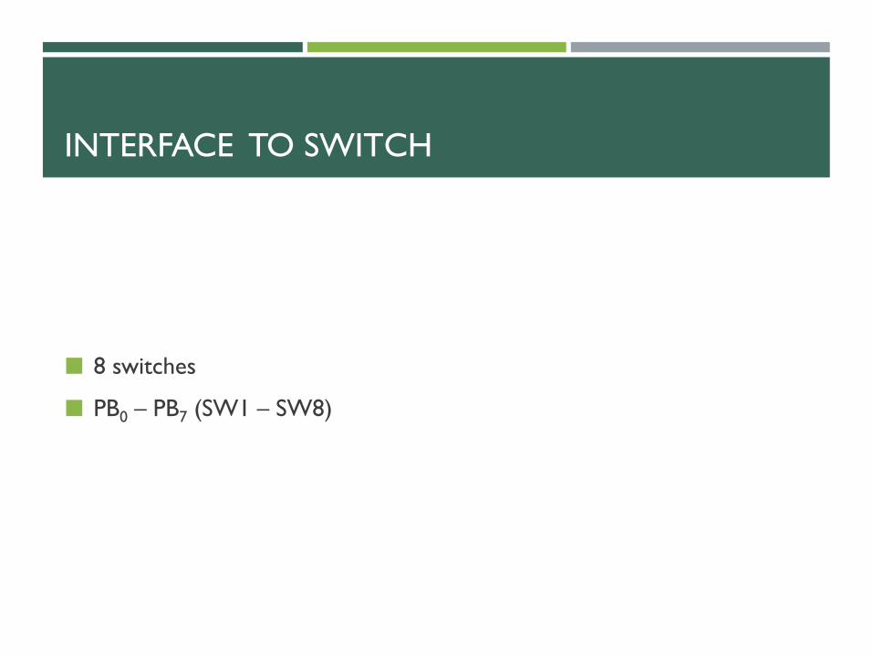
INTERFACE TO SWITCH
8 switches
PB0 – PB7 (SW1 – SW8)

7 SEGMENT DISPLAY
1 – seven segment displays
1- 7447
Requires 4-bit

7447
AB CD
a
h
LTRBO RBI
5V
Vcc 5VGND
D0
PC0
PC1
PC2
PC35V

1 SEC INTERRUPT
Use 8253 as only that is available in proteus
Clock has to be generated using pulse generator
using 10KHz – if a higher frequency is used – pulse
will not be proper- as rise and fall time of pulse in
proteus can be set to a minimum of 1µs – and the
rise and fall time are should be less than 1 % of
frequency.

CLK0
GATE0
OUT010 KHz
5V
OUT1
GATE1
CLK1
1 Hz
Count = 10000d
mode3
CLK2
GATE2
OUT2
TIMER INT

INTERRUPT GENERATION
Use 8259
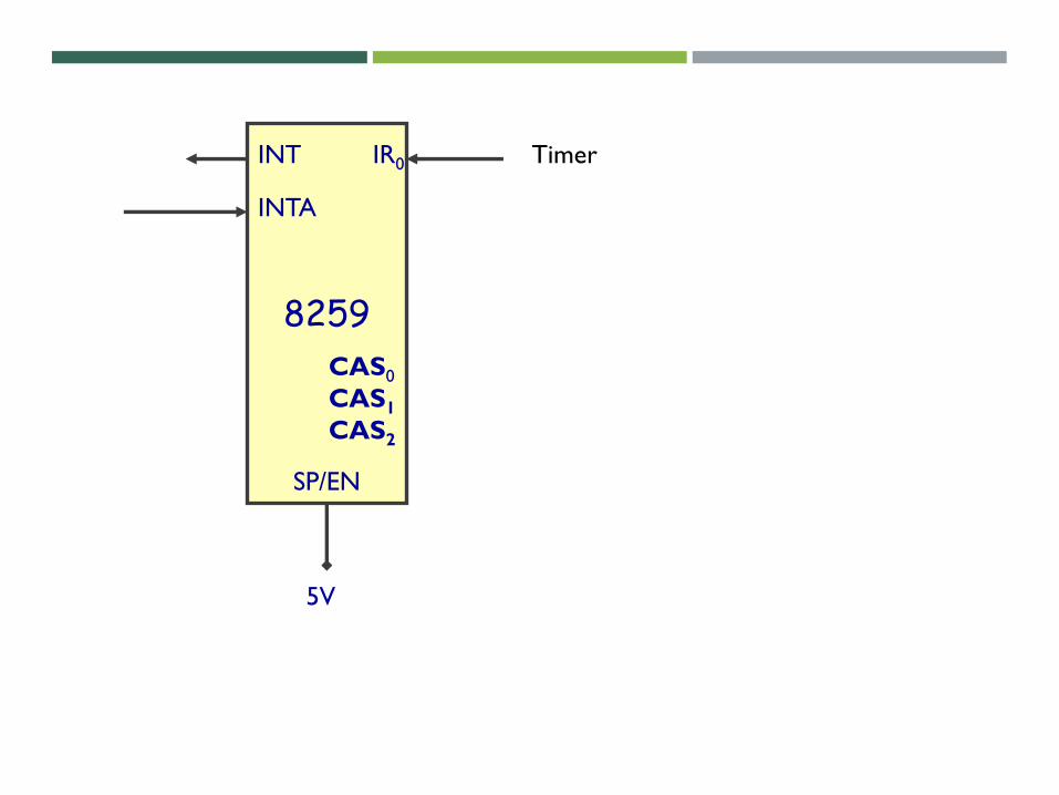
8259
IR0INT
INTA
CAS0
CAS1CAS2
SP/EN
5V
Timer

INTERFACE 8255, 8254 & 8259
Fixed addressing
Address
00 - 06H -8255
08H - 0EH – 8254
10H – 12H - 8259
Incremental Addressing

LS138
A0
G2A G1
G2B
I2
I1
I0
A5
A4
A3 O1
8254
O0
O2
8255
8259
M/IO’
GND

INTERFACE MEMORY
RAM – minimum 2k chip- 4k
ROM – in proteus 7 is minimum 4k chip – 8k
ROM1 00000H - 01FFFH
This is ok as proteus allows you to set reset address I have set it to 0000:0400(CS:IP)
This the area after IVT
RAM 02000H – 02FFFH

RAME
A13
M/IO’ A0
BHE’ RAMO
ROME
A13
M/IO’ A0
BHE’ ROMO

Interface to the processor
8255
A0
A1
A1
A2
CS
RD
WR
RD
WR
D0 – D7D0 – D7
RESETRESET from switch

Interface to the processor
8255
A0
A1
A1
A2
CS
RD
WR
RD
WR
D0 – D7D0 – D7
RESETRESET from 8284

8086
A16-A19
S6-S3
BHE’/S7
LS373
G
ALE
LS373
G
LS373
G
AD8-AD15
AD0-AD7
OE’
OE’
OE’
A16-A19
BHE’
A8-A15
A0-A7
MN/MX’ 5V
System Bus of 8086 (Address)

8086AD8-AD15
AD0-AD7
MN/MX’ 5V
LS245
DIR
LS245
OE’
OE’DIR
DT/R’
DEN’
D8-D15
D0-D7
RD
WR
IO/M
System Bus of 8086(Data + Control)

CLK (internal to 8086 in proteus)
RESET
MN/MX
READY
VCC
GND
HOLD
NMI
5 V
8086 Inputs
SP-DBT –
with
momentary
close

Software
Main
Branch to end of IVT
Initialize 8255,8254,8259
A
A
Read Switch
Display SW No.
Wait for1 sec

Software - ISR
ISR 1
Read Switch
Display
IRET

Program
Use EMU 8086 for assembling – as it creates the
reqd binary file to load to 8086 ROM