prototype design and testing of efficient metal …
TRANSCRIPT

PROTOTYPE DESIGN AND TESTING OF EFFICIENT METAL
PRINTED CIRCUIT BOARDS (M-PCBS) AS HEAT SINK FOR
HIGH POWER LEDS
by
ONG ZENG YIN
Thesis submitted in fulfilment of the requirements
for the degree of
Master of Science
January 2016

ii
ACKNOWLEDGEMENTS
My upmost gratitude is to my Lord almighty God whose grace and blessings are
upon me through the years of my post-graduate research. Whom also provide me
strength, wisdom and guidance to complete this thesis.
I would like to express my sincere gratitude and deep appreciation to my
main supervisor, Assoc. Prof. Dr. Mutharasu Devarajan for his valuable guidance
and big effort in supporting and motivating me throughout the whole period of the
research. I also give my sincere thanks to Dr. Shanmugan Subramani for his many
guidance and valuable inputs in this research project. I am most grateful with the
huge financial support provided by Collaborative Research in Engineering, Science
and Technology (CREST) under grant (304/PFIZIK/650601/C121) in completing
this research project.
I give my special thanks to all lab technicians from Nano Optoelectronics
Research Lab (NOR) for the technical support on the research equipment. Also
thanks to Mohamed Mustaqim Abu Bakar from X-Ray Crystallography Lab who is
helping in data acquisition. Unforgotten to give my gracious thanks to my lab
colleagues who’s together facing both hardness and joy in research. Thanks for the
kindness and hospitality in practical works and sharing ideas and experience together
throughout the years of the research.
Last but not least, a warm and utmost appreciation must be expressed to my
family members for the strong love, encouragement and the financial support for my
post-graduate research journey. Thank you.
Ong Zeng Yin

iii
TABLES OF CONTENTS
Page
Acknowledgement …………………………………………………………………..ii
Table of contents ……………………………………………………………………iii
List of Tables ………………………………………………………........................vii
List of Figures ……………………………………………………………………..viii
List of Plates ………………………………………………………………………..xi
List of Abbreviations …………………….………………………………………...xii
List of Symbols ………………………………………………….……………...…xiii
Abstrak …………………………………………………………………….............xv
Abstract ………………………………………………………………...................xvii
CHAPTER 1 INTRODUCTION ............................................................................1
1.1 Overview ........................................................................................................1
1.2 Introduction………………………….............................................................1
1.3 Problem Statement ……………………………………………………..........1
1.4 Objectives ……………………………………………………………….......4
1.5 Research Contribution……………………………….……………..….…….4
1.6 Thesis Outline ……………………………………………………...………..4
CHAPTER 2 LITERATURE REVIEW ……………………….……….……….7
2.1 Overview …………………………………………………….………….......7
2.2 Thermal Management of Light Emitting Diodes (LEDs)…………...……....7
2.3 Design of Printed Circuit Board (PCB) in Thermal Solution……..…...……9
2.4 Thin Film Coating as Effective Interface Material …………………….......10
2.5 Thin Film Deposition ………………………………………………............12

iv
2.6 Research Gap…………………………………………………………….….14
CHAPTER 3 THEORETICAL BACKGROUND ………………………….…..16
3.1 Overview …………………………………………………………..……..…16
3.2 Group III Nitrides ……………………………………..………………........16
3.2.1 Aluminium Nitride …………………………………………….…....16
3.2.2 Boron Nitride ………………………………….………………..…..17
3.3 Chemical Vapour Deposition (CVD) ……………………………................17
3.3.1 CVD System ………………………………………………….….....17
3.3.2 Precursor Consideration …………………………………….……...19
3.3.3 Precursor Bubbling Method ………………………………...……...20
3.4 Principle of 1-D Heat Transfer …………………………………………......21
3.5 Thermal and Optical Relation in Thermal Measurements ……....................23
CHAPTER 4 METHODOLOGY …………………………………..……….......25
4.1 Overview ……………………………………………………....……….......25
4.2 Thin Film Synthesis ………………………………………………..…........26
4.2.1 Substrates’ Preparation ………………………………..……...........26
4.2.2 DC & RF Co-Sputtering Technique……………………….…….....27
4.2.3 Chemical Vapour Deposition (CVD) Technique ………….…........29
4.2.3.1 Ceramic Tube Furnace System ………………….…........30
4.2.3.2 Combined Furnaces System …………………………..…31
4.2.3.3 Precursor Bubbling System ………………………….…..31
4.3 Structural Characterizations ……………………………….........................34
4.3.1 X-Ray Diffraction Analysis …………………………….................35
4.3.2 Surface Topography Analysis ………………………………..........36

v
4.4 Prototype PCB Fabrication ………………………………………..…..…..36
4.5 Thermal Characterization ………………………………............................38
4.5.1 Thermal Measurement – Thermal Substrates ……………..….......40
4.5.2 Thermal Measurement – Prototype M-PCBs …………….….........41
4.6 Optical Characterization ……………………………….……....................42
4.6.1 Spectrometer Measurement ………………………………..…......42
4.6.2 Industrial Optical Measurement ………………………….………43
CHAPTER 5 RESULTS AND DISCUSSION ………………………………...44
5.1 Overview ……………………………………………………………….....44
5.2 Experimental Observations of CVD Process …………………..….….......44
5.2.1 Ceramic Tube Furnace System …………………………….…..…45
5.2.2 Combined Furnaces System ……………………………….….......46
5.2.3 Precursor Bubbling System …………………………………....….47
5.3 XRD Results of B-AlN Thin Film Coated Al Substrates ……………........47
5.3.1 XRD Spectra of B-AlN by
Co-Sputtering Method …………………………………….........…48
5.3.2 XRD Spectra of Thin Film by
CVD Method (Gas Flow Rate) ……………………………..…......49
5.3.3 XRD Spectra of Thin Film by
CVD Layer Stacking Method ………………………………..........50
5.3.4 Structure Properties of B-AlN Thin Films ………………………...51
5.4 AFM Results of B-AlN Thin Film Coated Al Substrates ……………........55
5.5 Thermal Characterization ………………………………………….....…...58
5.5.1 Thermal Measurement Results of Thermal Substrates …...…........58
5.5.1.1 Total Thermal Resistance of LED System with
Thermal Substrates ………………………………...........59
5.5.1.2 Substrate Thermal Resistance of

vi
Thermal Substrates ………………………………............61
5.5.1.3 Rise in Junction Temperature of LED on
Thermal Substrates ………………………………….…...62
5.5.2 Thermal Measurement Results of Prototype M-PCBs…………......64
5.5.2.1 Total Thermal Resistance of LED on M-PCBs …....….....65
5.5.2.2 PCB Thermal Resistance of M-PCBs …………………....67
5.5.2.3 Rise in Junction Temperature of LED on M-PCBs ….......68
5.6 Optical Characterization …….......................................................................70
5.6.1 Optical Results of Thermal Substrates ………………………….....70
5.6.1.1 Optical Behaviour with Various Driving Currents of
Thermal Substrates ……………………….……….…......71
5.6.1.2 Illuminance of 3W Green LED Package on
Thermal Substrates …………………………...….............72
5.6.2 Optical Results of Prototype M-PCBs …………………...……...…74
5.6.2.1 Correlated Colour Temperature (CCT) of LED on
M-PCBs …………………………………………...…......75
5.6.2.2 Illuminance of LED on M-PCBs ……………….............76
5.7 Performance Comparison of Prototype M-PCBs with MCPCB ..................77
5.7.1 Thermal Performance Comparison ……………………….…....….78
5.7.2 Optical Performance Comparison …………………………..….….81
CHAPTER 6 CONCLUSIONS …………………………………………….........88
6.1 Conclusions of the Study …..………………………………………............88
6.2 Recommendations for Future Research…………………………..…….......89
REFERENCES ……………………………………………………….……....…..93
APPENDICES ………………………………………………….…………...…...103
LIST OF PUBLICATIONS………………………………………….…….……116

vii
LIST OF TABLES
Page
Table 2.1 Thermal resistance (Rth) of various interface material 11
on Cu substrates
Table 4.1 Process parameters of co-sputtering depositions 28
Table 4.2 Various gas flow rates of CVD process 33
Table 4.3 Average thickness of B-AlN muti-layers 34
Table 4.4 Average Thickness of screen printed PCB layers 38
Table 5.1 XRD analysis data of B-AlN thin films 52
Table 5.2 Structural properties of c-AlN peak from 53
various processes
Table 5.3 Summarized Rth-sub of Thermal Substrates 62
Table 5.4 Summarized Rth-sub of M-PCBs 67
Table 5.5 Summarized CRI values of LED on Thermal Substrates 71
Table 5.6 Summarized CRI values of LED on M-PCBs 74
Table 5.7 Structural comparison of MCPCB and M-PCB 77

viii
LIST OF FIGURES
Page
Figure 1.1 Structure of typical PCB: (a) FR4 PCB, (b) MCPCB 2
Figure 1.2 Simulated heat flow and Tj of (a) FR4 PCB, (b) MCPCB 3
Figure 2.1 One dimensional heat flow path in a typical high power 8
LED system
Figure 2.2 Thermal resistance model of LED system 9
Figure 2.3 Schematic structure of SuperMCPCB and MCPCB 9
by N. Wang et al.
Figure 2.4 Cumulative structural function of MCPCB and Al2O3 10
deposited MCPCB by H.M. Cho et al.
Figure 2.5 Thermal resistance (Rth) comparison of BN coated Cu substrate 11
with different boundary conditions
Figure 2.6 Cumulative structural function of LED mounted on Al substrate 12
with various interface boundary conditions
Figure 2.7 Schematic diagram of molecular beam epitaxy (MBE) 13
Figure 2.8 Schematic diagram of sputtering process 13
Figure 3.1 Typical set-up of a CVD system 18
Figure 3.2 CVD reaction kinetics of in reaction zone 19
Figure 3.3 The flow mechanism of liquid precursor bubbler 21
Figure 3.4 One dimension heat transfer across a material 21
Figure 3.5 TIM applied to fill up the air gaps between two materials 22
Figure 4.1 Process flow chart of research methodology 25
Figure 4.2 Synthesis processes of B-AlN thin film depositions 26
Figure 4.3 Set-up of DC & RF Sputtering Process 27
Figure 4.4 The chronology of precursor choices and CVD set-ups in 30
optimization of CVD process
Figure 4.5 Schematic diagram of three zone ceramic tube CVD system 30

ix
Figure 4.6 Schematic diagram of three zone and single zone quartz tube 31
combined CVD system
Figure 4.7 Schematic diagram of precursor bubbling method 32
of CVD system
Figure 4.8 Schematic diagram of multi-layer stacked thin films 34
on Al substrate
Figure 4.9 The process flow of PCB fabrication by screen printing 36
Figure 4.10 Design model of prototype M-PCB 37
Figure 4.11 Golden Dragon white LED mounted on M-PCB 38
Figure 4.12 Schematic diagram of 3W green LED package mounted 40
on Thermal Substrate
Figure 4.13 K-factor of 3W green LED package 41
Figure 4.14 Schematic diagram of Golden Dragon White LED mounted 41
on M-PCB
Figure 4.15 Optical measurement set-up of DUT in still air chamber 42
Figure 5.1 XRD spectra of co-sputtered B-AlN thin films by 48
various processes
Figure 5.2 XRD spectra of B-AlN thin films deposited by 50
various CVD processes
Figure 5.3 XRD spectra of B-AlN thin films deposited layer stack method 51
Figure 5.4 Crystallite size of c-AlN peak from various processes 54
Figure 5.5 3D surface images of B-AlN thin films by various processes 56
Figure 5.6 Surface roughness of B-AlN by various processes 57
Figure 5.7 Schematic diagram of 3W LED mounted on Thermal Substrate 58
Figure 5.8 Cumulative structure function measured LED package on 59
Thermal Substrate
Figure 5.9 Total thermal resistances (Rth-tot) of Thermal Substrates by 60
various processes
Figure 5.10 Rise in junction temperature of Thermal Substrates 63
Figure 5.11 Schematic diagram of M-PCB 64

x
Figure 5.12 Cumulative structural function of LED on M-PCB 64
Figure 5.13 Total thermal resistances (Rth-tot) of M-PCBs by various 66
processes
Figure 5.14 Rise in junction temperature of M-PCBs 69
Figure 5.15 Variation of LUX level in 15 minutes of LED on 72
Thermal Substrates
Figure 5.16 LUX level of LED package on Thermal Substrates 73
Figure 5.17 CCT comparison of M-PCBs at various driving currents 75
Figure 5.18 LUX level of LED package on M-PCBs 76
Figure 5.19 Cumulative structural function of LED on various PCBs 78
Figure 5.20 Rth-tot comparison of MCPCB with M-PCBs 79
Figure 5.21 Rth-pcb comparison of MCPCB with M-PCBs 79
Figure 5.22 ΔT comparison of LED on various PCBs 81
Figure 5.23 CCT comparison of MCPCB and M-PCBs at various 82
driving currents
Figure 5.24 The LUX level comparison of MCPCB and M-PCBs at 82
various driving current.
Figure 5.25 A. Luminous flux and, B. Efficacy of LED on various PCBs 83
Figure 5.26 CIE 1931 colour coordinate plot of LED on PCBs at 100 mA 84
Figure 5.27 CIE 1931 colour coordinate plot of LED on PCBs at 350 mA 85
Figure 5.28 CIE 1931 colour coordinate plot of LED on PCBs at 700 mA 85
Figure 6.1 Reaction kinetics of (a) Thick and (b) Thin boundary layers 91
Figure 6.2 Simulated flow of current CVD process 92
Figure 6.3 Simulated flow of suggested substrates’ holder 92
xi
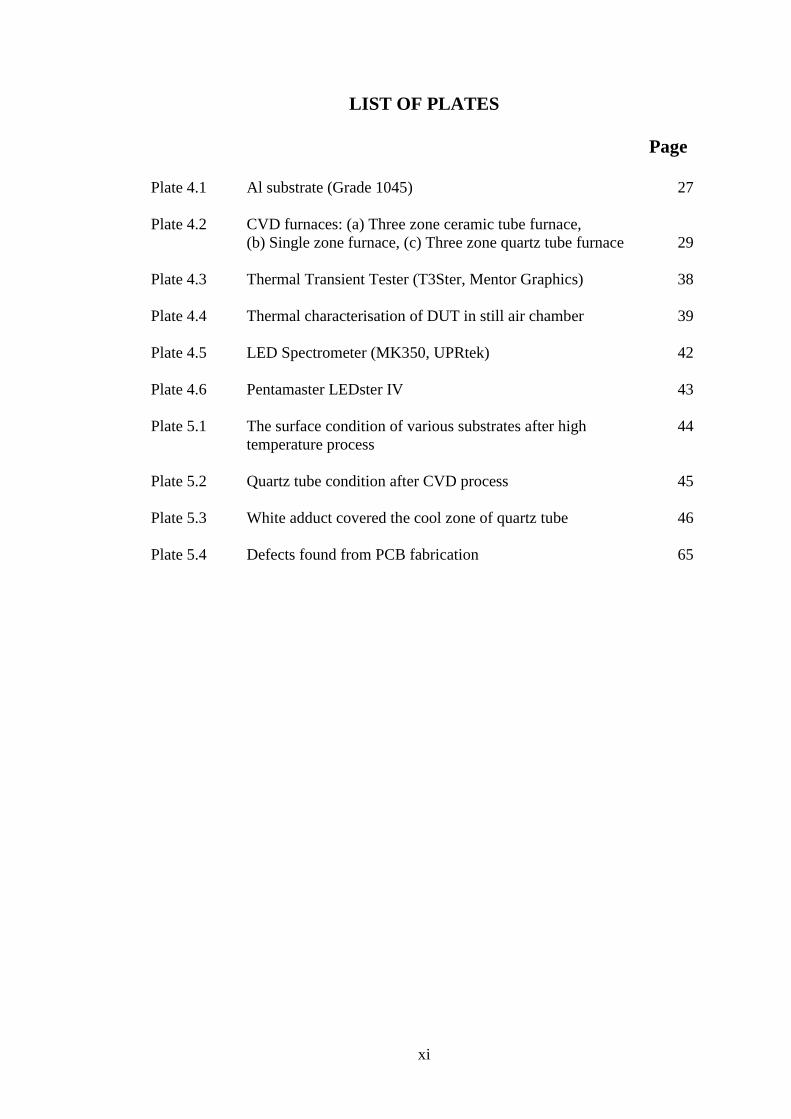
LIST OF PLATES
Page
Plate 4.1 Al substrate (Grade 1045) 27
Plate 4.2 CVD furnaces: (a) Three zone ceramic tube furnace,
(b) Single zone furnace, (c) Three zone quartz tube furnace 29
Plate 4.3 Thermal Transient Tester (T3Ster, Mentor Graphics) 38
Plate 4.4 Thermal characterisation of DUT in still air chamber 39
Plate 4.5 LED Spectrometer (MK350, UPRtek) 42
Plate 4.6 Pentamaster LEDster IV 43
Plate 5.1 The surface condition of various substrates after high 44
temperature process
Plate 5.2 Quartz tube condition after CVD process 45
Plate 5.3 White adduct covered the cool zone of quartz tube 46
Plate 5.4 Defects found from PCB fabrication 65

xii
LIST OF ABBREVIATIONS
LED Light emitting diode
PCB Printed circuit board
MCPCB Metal core printed circuit board
TIM Thermal interface material
BLT Bond line thickness
XRD X-ray diffraction
AFM Atomic force microscope
FESEM Field emission scanning electron microscope
DUT Device under Test
M-PCB Metal-printed circuit board
CCT Correlated colour temperature
CRI Colour rendering index
LUX Illuminance

xiii
LIST OF SYMBOLS
Rth Thermal resistance
TJ Junction temperature
ΔTJ Rise in junction temperature
Q Heat source
T Temperature
A Cross-sectional area
k Thermal conductivity
kTIM Thermal conductivity of TIM
Reffective Effective thermal resistance
Rc Contact resistance
PI Input electrical power
Popt Output optical power
PH Heat dissipation power
Pthermal Thermal power
V Forward voltage
D Crystallite size
λ Wavelength of radiation
β Full width at half maximum (FWHM)
θ Bragg diffraction angle of (hkl)
σ Internal stress
d d-spacing
E Young’s modulus
Y Poisson’s ratio

xiv
ε Mirco-strain
Ra Surface roughness
Itot Total current
Isc Sensor current
Iin Input current
ΔVF Difference in temperature-sensing voltage
K Sensitivity value (K factor)
Rth-tot Total thermal resistance
Rth-sub Substrate thermal resistance
Rth-pcb PCB thermal resistance

xv
REKA BENTUK PROTOTAIP DAN UJIAN BAGI PAPAN LITAR
BERCETAK LOGAM (M-PCBS) YANG CEKAP SEBAGAI SINK HABA
UNTUK LEDS KUASA TINGGI
ABSTRAK
Dalam penyelesaian cabaran haba diod pemancar cahaya (LED) beroperasi,
suatu penyiasatan atas reka bentuk papan litar bercetak (PCB) haba cekap telah
menarik perhatian banyak industri. Papan litar bercetak berteras logam (MCPCB)
telah menjadi pilihan yang sangat baik. Walaupun ia merupakan penyebar haba yang
sangat baik dalam mengurangkan suhu berlebihan pada simpang LED, fabrikasi
MCPCB melibatkan pelbagai langkah proses dan beberapa lapisan. Lebih banayk
lapisan PCB mewujudkan rintangan haba (Rth) tinggi yang disumbangkan oleh
beberapa lapisan antara muka. Oleh itu, mengenal pasti bahan konduktif haba yang
tinggi pada substrat logam degan lapisan antara muka yang minimum untuk
pemindahan haba yanng lebih baik dan operasi LED yang cekap. Dalam kajian ini,
boron doped aluminium nitride (B-AlN) filem nipis pada Al substrat telah disediakan
oleh dua jenis teknik yang berlainan iaitu permecikan bersama arus terus (DC)
dengan frekuensi radio (RF) dan penmendapan wap kimia (CVD) bersuhu rendah
pada tekanan atmosfera dengan precursor alternatif. Parameter sintesis telah diubah
dan dioptimumkan untuk mendapatkan kualiti B-AlN filim nipis yang baik. Antara
teknik sintesis, filem yang disediakan oleh kaedah CVD menunjukan sifat-sifat
struktur yang lebih baik dan telah dipilih untuk fabrikasi PCB prototaip. Sebelum
fabrikasi PCB, Al substrat dilapisi B-AlN telah diuji prestasi terma dan optik sebagai
sink haba (Thermal Substrates) dengan menggunakan kaedah analisis fana LED
kuasa tinggi dan LED spektrometer. Beberapa prototaip PCB (M-PCBs) akhirnya
dibina pada Al substrat dilapisi B-AlN dan diuji prestasi terma dan optik dengan
LED kuasa tinggi yang dipasang pada prototaip. Perbandingan antara M-PCB dengan

xvi
MCPCB komersial menunjukkan bahawa M-PCB disediakan daripada B-AlN filem
nipis dilapisi dengan paramter proses CVD (CVD 4) mempunyai prestasi terma yang
lebih baik daripada MCPCB pada keadaan operasi yang sama. Pada arus elektrik 700
mA, M-PCB ketara mencapai Rth-tot dan Rth-pcb yang lebih rendah berbandign dengan
MCPCB. Kenaikan suhu simpang (ΔTJ) telah dikawal dan dikurangkan secara drastik
dari 65.77 °C ke 52.55 °C bagi kegunaan M-PCB berbanding dengan MCPCB. Nilai
suhu warna berhubung kait (CCT) LED pada M-PCB diuji dengan 700 mA adalah
lebih rendah (≈8100 K) bila berbanding dengan MCPCB komersial (≥10000 K) dan
warna cahaya dieleakkan beralih kepada warna ―biru‖. Didapati bahawa M-PCB juga
menunjukkan peningkatan fluks cahaya (68.38 lm) berbanding dengan MCPCB
(61.83 lm).
xvii
PROTOTYPE DESIGN AND TESTING OF EFFICIENT METAL PRINTED
CIRCUIT BOARDS (M-PCB) AS HEAT SINK FOR HIGH POWER LEDS
ABSTRACT
In solving the thermal challenges in LED operation, an investigation on
designing the thermally efficient printed circuit board (PCB) has drawn the attention
of many industries. Metal-core printed circuit board (MCPCB) has been an excellent
choice. Though it is an excellent heat spreader in reducing the excessive temperature
at the LED junction, the fabrication of MCPCB involves various process steps and
number of layers. More PCB layers create high thermal resistance (Rth) which is
contributed by several interface layers. Therefore, it is necessary to identify high
thermal conductive material on metal substrate with minimal interface layers for
better heat transfer and efficient LED operation. In this research, boron doped
aluminium nitride (B-AlN) thin films on Al substrates were prepared by two
different techniques which are DC & RF co-sputtering and low temperature chemical
vapour deposition (CVD) at atmospheric pressure with alternative precursor. The
synthesis parameters were varied and developed to obtain good quality B-AlN thin
film. Among the synthesis techniques, films prepared by CVD method showed better
structural properties and were chosen for fabrication of prototype PCBs. Prior to the
PCB fabrication, B-AlN coated Al substrates were tested for their thermal and optical
performances as heat sink (Thermal Substrates) using transient analysis method of
the high power LED and LED spectrometer. Several prototype PCBs (M-PCBs) were
eventually fabricated on B-AlN coated Al substrates and tested for their thermal and
optical performances with high power LEDs mounted on prototypes. The comparison
between M-PCB and commercial MCPCB had shown that the M-PCB prepared from
B-AlN thin film coated by CVD process (CVD 4) had better thermal performance
than MCPCB. At 700 mA driving current, M-PCB significantly achieved lower Rth-tot

xviii
and Rth-pcb as compared to MCPCB under the same operating condition. The rise in
junction temperature of LED (ΔTJ) was controlled and reduced drastically from
65.77 °C to 52.55 °C by using M-PCB as compared to that with MCPCB. The
correlated colour temperature (CCT) value of the LED on M-PCB at 700 mA was
lower (≈8100 K) when compared with commercial MCPCB (≥10000 K) and avoided
the colour shifting towards ―bluish‖ colour. It was found that M-PCB also showed
increased luminous flux (68.38 lm) as compared with MCPCB (61.83 lm).

1
CHAPTER 1
INTRODUCTION
1.1 Overview
The chapter includes a brief introduction to thermal challenges in LEDs, the current
problem faced in this field, the contribution and output of the project, the research
objectives and the outline of the whole thesis.
1.2 Introduction
Light Emitting Diode (LED) is a low energy consumption semiconductor light
source. In the advancement of the luminescence technology, the evolution of LED
has great impact in lighting solutions over the years. It provides better optical
performance than incandescent/halogen light with the efficiency of visible light
output can be improved to approximately 10-20 %, and it has much longer lifetime
than traditional light source [1-2].
However, the miniaturization of LED package design with the increase in
current density has challenged the thermal management of LED. The heat dissipation
through small size devices can be more than their predecessors which have larger
package size. Approximately 70-90 % of energy is converted into heat in LED
package [3-4]. Thus, better thermal management techniques must be implemented to
dissipate the large amount of heat from the package.
1.3 Problem Statement
Thermal impedance between the components and PCB is the main issue in solid state
lighting, which may contribute high thermal resistance (Rth) and excessive rise in
junction temperature (ΔTj) of LED packaging. Consequently, it will negatively affect

2
the lifetime, brightness, and colour uniformity of the light output, excessive Tj may
also lead to device damage or failure [5-6]. Thus, thermal management of high power
devices like LEDs has become more and more critical aspect of LED system design.
In order to overcome the thermal problem, sufficient heat removal is essential
from LED chip to ambient. The design in structure and thermal conductive material
of Printed Circuit Boards (PCBs) is suggested for thermal management in solid state
lighting. One of the popular approaches to compensate the thermal problem in PCB
is the design of Metal Core Printed Circuit Board (MCPCB), which consists of thick
metal base substrate, thin dielectric layer and the circuitry layer. FR4 PCB consists of
copper layers cladded on top and bottom of thick FR4 substrate. The structures of
typical FR4 PCB and MCPCB are presented in Fig. 1.1. The thermal performance
comparison of both FR4 PCB and MCPCB in terms of Tj obtained from simulation
software (Mentor Graphics FloEFD 11) is shown in Fig. 1.2.
Figure 1.1 Structure of typical PCB: A. FR4 PCB, B. MCPCB

3
Figure 1.2 Simulated heat flow and Tj of: A. FR4 PCB, B. MCPCB
At 1 W of heat source generated on the LED chip, the results from the simulation
show that MCPCB performs better in removing heat from junction to ambient. Due
to low thermal conductivity of thick FR4 layer, the heat is trapped at the heat slug of
the LED package. Since the advantage of MCPCB is the thick metal substrate, the
dielectric material has become the key property which will determine the thermal
effectiveness of MCPCB. Therefore, to meet the increasing demand of thermal
requirement of the high power dissipation PCBs, it is vital to improve the thermal
path of PCBs by suggesting and designing new structure and material of PCB.
Thin film coating is suggested as interface material and also heat spreader to
enhance the thermal path of PCB and chemical vapour deposition (CVD) method is
proposed for thin film synthesis in this project. However the CVD synthesis of
nitride thin film on metal substrate has not been reported so far due to high
temperature requirement (≥ 800 °C), which is not suitable for metal substrates with
low melting point. Therefore, alternative CVD method has to be established in
attempt to deposit nitride thin film on metal substrate.
4
1.4 Objectives
There are three objectives to achieve in this study:
To synthesize Boron doped Aluminium Nitride (B-AlN) thin film layer on
Aluminium (Al) substrates using DC/RF co-sputtering and Chemical Vapour
Deposition (CVD) methods with varying their parameters.
To investigate the thermal and optical performances of LED package with B-
AlN thin film coated Al substrate as efficient heat sink.
To design and fabricate a prototype metal PCB (M-PCB) with B-AlN thin
film coated Al substrate and compares the thermal and optical performances
of LED between MCPCB and M-PCB.
1.5 Research Contribution
As the outcome of this project, a ceramic thin film coated prototype Metal-PCB (M-
PCB) for high power LED is delivered. In addition, the low cost CVD synthesis
technique of thin film coating on metal substrate is developed for PCB fabrication
industries.
1.6 Thesis Outline
This thesis is divided into six major chapters, which are introduction, literature
review, theoretical background, methodology, results and discussion, and conclusion.
i) Chapter 1 : Introduction
This first chapter provides general introduction about LED and
importance of thermal management in high power LED. Then followed
by the problem statement which states the issues with LED heat

5
dissipation that lead to this research. The objectives are presented and it
also includes research contribution of the project.
ii) Chapter 2 : Literature Review
This second chapter presents the literatures of the LED thermal
management, some research backgrounds of PCBs, thermal applications
of thin film and deposition methods with CVD and other related processes,
and includes the reviews of all the previous works which had been done
or discovered by other people and authors. Besides, the advantages and
disadvantages of some common synthesis methods such as CVD, PVD,
and Molecular Beam Epitaxy (MBE) are discussed.
iii) Chapter 3 : Theoretical Background
In third chapter, the general introduction of group III nitrides thin films is
discussed. The CVD system and process are discussed extensively here.
The descriptions of the thermal and optical performances of LED are also
included in this chapter.
iv) Chapter 4 : Methodology
This chapter describes in the methodology of this project, which begins
with substrates preparation, process development, PCB fabrication, LED
characterization and data analysis.
6
v) Chapter 5 : Results and Discussion
This chapter presents the results of the data collected from the thin film
analysis and LED thermal and optical characterizations. The results are
also presented in forms of graphics and figure from analysis equipment.
vi) Chapter 6 : Conclusions and Recommendations
In this last chapter, the results of the work are summarized and
conclusions are presented. Future suggestions and recommendations to
enhance and further carry out this research are also included in this
chapter.

7
CHAPTER 2
LITERATURE REVIEW
2.1 Overview
This chapter presents the concept and mechanism of heat transfer and thermal
management of LED packages. The studies and reports of researches on
enhancement of heat dissipation in high power devices are also included. The focuses
of this chapter are:-
Thermal Management of LED System
Designs of Printed Circuit Board (PCB) in Thermal Solution
Thin Film Coating as Effective Interface Material
Thin Film Deposition Methods
2.2 Thermal Management of Light Emitting Diodes (LEDs)
When power is applied on LED chip, luminescence reaction occurs at the p-n
junction semiconductor material and only a portion of energy is converted into light
output. The rest of the energy is then turn into the form of heat which must be
removed from the LED chip. Unlike traditional incandescent bulbs, LED does not
radiate heat; thermal conduction is the only way to dissipate the excessive heat [7].
Fig. 2.1 describes the heat conduction in typical high power LED from p-n junction
to the PCB followed by external heat sink into the ambient.

8
Figure 2.1 One dimensional heat flow path in a typical high power LED system
In general, the higher the input power, the greater the amount of heat
generated at the LED chip. Proper thermal path must be established in order to
remove the great amount of heat effectively from the chip into the surrounding
through conduction. LEDs’ chip today can only endure up to 150 °C [8]. Heat must
be removed properly from LED chip to ambient in order to maintain the expected
lifetime, light output and colour.
To describe the thermal system of LED package, the system can be simplified
and illustrated using thermal resistance model as shown in Fig 2.2 [9]. The model is
analogous to an electrical circuit, where heat source (Q) is represented by current
source, heat flow is represented by current, the voltage is represented temperature (T),
and resistor is represented the thermal resistance (Rth).
The two basic parameters to evaluate LED performance are junction
temperature (Tj) and thermal resistance (Rth). The heat generation at the p-n junction
has the highest temperature in LED package which is the Tj. The capability of heat
transfer across the whole LED system determines the Tj of the LED chip. So the
major impact of LED performance lies on the design of thermal path from chip to
ambient.

9
Figure 2.2 Thermal resistance model of LED system
2.3 Design of Printed Circuit Board (PCB) in Thermal Solution
There are several works on designing thermal efficient PCB have been
reported in literature. Wang et al. [10] evaluated the thermal performance of Direct
Plated Copper (DPC) ceramic substrate and custom designed SuperMCPCB with
extended heat spreader as shown in Fig. 2.3, which shows better performance than
conventional MCPCB. There is another work on designing DPC ceramic spreader
which also shows better performance over MCPCB [11].
It was reported by Shen et al. [12] that with 30 % diamond powder filled
dielectric layer has 36 % reduction of Rth as compared to typical MCPCB. It is also
reported of using high thermal conductive nitride fillers for the improvement of
thermal conductivity [13]. Besides that, reduction in Rth of 4-5 K/W is reported on
MCPCB with dense alumina thin film deposited by aerosol deposition method as
presented in Fig. 2.4 [14].
Figure 2.3 Schematic structure of SuperMCPCB and MCPCB by Wang et al. [10]

10
Figure 2.4 Cumulative structural function of MCPCB and Al2O3 deposited MCPCB
by Cho et al. [14]
2.4 Thin Film Coating as Effective Interface Material
In designing effective thermal system in high power devices, heat sink has become
the key component. Works on designing effective heat sinks had been carried out in
order to dissipate heat from device into ambient [15-17]. However, the contact area
between LED package and heat sink has significant effect on the thermal path of
whole system [18]. Thermal interface material (TIM) has been the common solution
in this issue [19] and grease has been a popular type of TIM in increase total contact
area between two materials [20,21].
There are several works reported on the use of thin film as effective TIM for
LED system at noticeable improvement is achieved at high driving current. Before
this project, some preliminary research works were done on sputtered AlN [22] and
BN [23] thin films on Cu substrates as TIM of heat sink for high power LED. The
evidences of improvement in thermal performance are shown in Table 2.1 and
Fig. 2.5, the Rth values of AlN and BN coated Cu substrate are lower as compare with
bare substrate and thermal paste applied substrate.
11
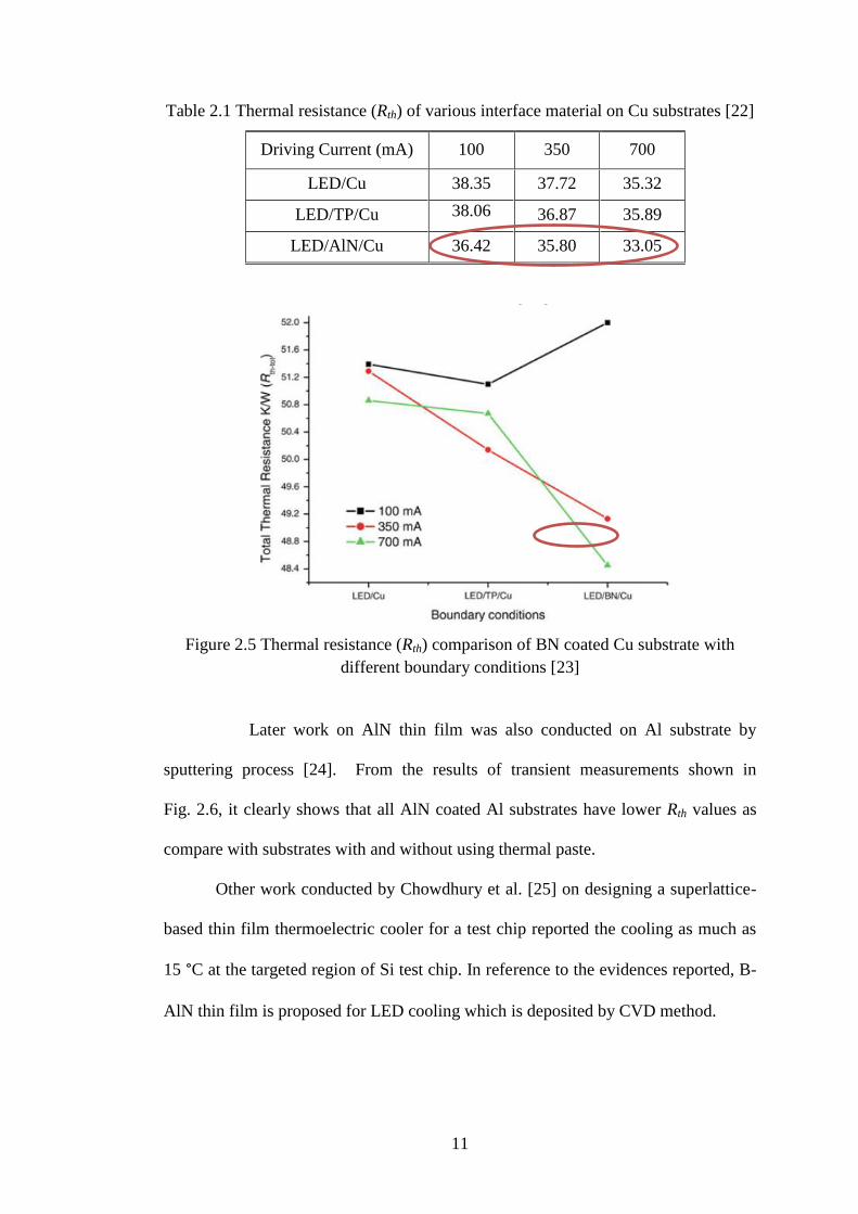
Table 2.1 Thermal resistance (Rth) of various interface material on Cu substrates [22]
Driving Current (mA) 100 350 700
LED/Cu 38.35 37.72 35.32
LED/TP/Cu 38.06 36.87 35.89
LED/AlN/Cu 36.42 35.80 33.05
Figure 2.5 Thermal resistance (Rth) comparison of BN coated Cu substrate with
different boundary conditions [23]
Later work on AlN thin film was also conducted on Al substrate by
sputtering process [24]. From the results of transient measurements shown in
Fig. 2.6, it clearly shows that all AlN coated Al substrates have lower Rth values as
compare with substrates with and without using thermal paste.
Other work conducted by Chowdhury et al. [25] on designing a superlattice-
based thin film thermoelectric cooler for a test chip reported the cooling as much as
15 °C at the targeted region of Si test chip. In reference to the evidences reported, B-
AlN thin film is proposed for LED cooling which is deposited by CVD method.

12
Figure 2.6 Cumulative structural function of LED mounted on Al substrate with
various interface boundary conditions [24]
2.5 Thin Film Deposition
Since many years, a variety of fabrication methods for AlN and BN thin films had
been reported. The common deposition techniques used in industry to synthesize thin
films are Sputtering [26-28], Molecular Beam Epitaxy (MBE) [29], Pulsed Laser
Deposition (PLD) [30,31], and Chemical Vapour Deposition (CVD) [32-34].
The MBE method (as shown in Fig. 2.7) gives the most precise control of the
thickness layer uniformity and doping, and it can produce highly abrupt junction
between different materials under low temperature with low percentage of defects
[35]. However, the cost is the most expensive among all the deposition methods and
it does not scale well for industrial production.
Sputtering and PLD are both physical vapour deposition (PVD) where the
film thickness and ally composition can also be controlled by fixing the operating
parameters and adjusting the deposition time. The basic sputtering process is shown
in Fig. 2.8. The main drawback in PVD method is low deposition rate due to the
limitation of power input on the target material.

13
Figure 2.7 Schematic diagram of molecular beam epitaxy (MBE) [35].
Figure 2.8 Schematic diagram of sputtering process [36]
On the other hand, CVD has the advantages over MBE and PVD in terms of
overall cost and high deposition rate. CVD reactor is relatively simple which can be
modified to accommodate higher number of substrates, and it does not require ultra-
high vacuum condition as in PVD. Another benefit of CVD is that it generally can be
adapted to many process variations for synthesis of different materials [37,38]. Film
formation relies upon the chemical reaction of precursors [39]. So CVD method is
the preferred choice in current reserach for the synthesis of B-AlN thin film.

14
In nitride CVD deposition, ammonia gas (NH3) has been the common
nitrogen source for nitride growth in CVD process [40,41]. However, high deposition
temperature (typically ≥ 1000 °C) is required due to high thermal stability of NH3.
Moreover the gas is toxic and requires proper exhaust system. The high temperature
seriously limits the choice of substrate material available as the substrate is
positioned at the highest temperature of deposition zone [42].
In attempt to reduce the deposition temperature, plasma-enhanced CVD
(PECVD) had been suggested [43,44] where plasma activated reactions can occur at
lower deposition temperature. However this technique is difficult to control and the
system is expensive. In addition, metal organic CVD (MOCVD) method has been
widely adopted to produce high quality nitride films [45,46]. The use of metal-
organic precursors such as hexakis(dimethylamido)dialuminum [Al2(NMe2)6] [47]
and trimethylaluminum [Al2(CH3)6] [48] have been developed to surmount the high
temperature problem, but the precursors are not easy to handle and not stable in the
presence of oxygen and moisture. There are some reports on utilizing attractive
single-source precursor such as trimethylaluminium ammonia [(Me3Al(NH3)] adduct
[49,50]. However the preparation of single-source precursors involves complex and
costly procedures.
2.6 Research Gap
In this work, the deposition temperature must be low (˂ 650 °C) to prevent
the melt of metal substrates in the synthesis of B-AlN thin films. In reference to the
reports on successive use of mixed precursor with Tert-buthylamine (tBuNH2) at
lower deposition temperature (400 – 600 °C) [51,52], the CVD method was
developed through the utilization of liquid tBuNH2 precursor as alternative

15
independent nitrogen source with better vapour pressure (340 Torr at 25 °C) [53]
instead of high thermal stable NH3.
In order to further enhance the thermal conductivity of AlN, boron was
chosen as dopant for AlN thin film. Some literatures reported that addition of Cr
[54,55] and Si [56] as dopant can enhance the properties of AlN, and some reported
that addition of Zr [57] and B [58] can improve the thermal conductivity of
composite materials. Very few works were conducted on combination of group III
elements as dopant in nitride film and they proved that boron doping can shrink the
lattice of AlN structure and thus improves the thermal conductivity [59,60]. In this
work, boron was introduced as dopant through the use of boron trichloride (BCl3)
precursor in deposition of B-AlN thin films.
16
CHAPTER 3
THEORETICAL BACKGROUND
3.1 Overview
This chapter focus on the introduction of group III nitrides on their characteristics
and applications of the field. The overall view of chemical vapour deposition (CVD)
in its principles, technology and mechanism is presented here. The basic theory of
thermal and optical relation in thermal resistance is also explained here.
3.2 Group III Nitrides
Group III-Nitride semiconductor materials like (Al, In, Ga)N are materials that have
excellent wide band gap semiconductors which are highly recommanded for modern
electronic and optoelectronic applications [61]. Recent research results related to
AlN, BN and InN are reviewed, focusing on the different growth techniques of
Group III-nitride crystals and epitaxial films, heterostructures and devices.
3.2.1 Aluminium Nitride
Aluminium nitride (AlN) is one of the most attractive non-oxide ceramic materials of
group-III nitrides. It is famous because of its unique properties such as good
electrical resistivity (1014 Ωcm) due to high energy gap (6.2 eV), high breakdown
voltage (15 kV/mm), low thermal expansion coefficient, high mechanical strength,
high thermal conductivity [260W/(mK)], high melting point and also high corrosion
resistance [62].
Theoretically the thermal conductivity of AlN is reported to be about 280
Wm-1
K-1
[63]. Kuo et al. [64] reported that the value of AlN thin film is lower at the
range of 0.4 – 26 Wm-1
K-1
. Another research reported thermal conductivity of

17
170 Wm-1
K-1
was achieved in AlN thin film [65]. The thermal conductivity is very
much depending on the deposition method and process conditions that affect the film
properties.
3.2.2 Boron Nitride
Boron Nitride BN is another attractive nitride material which has high thermal
conductivity, chemical inertness, very high hardness and high resistivity. Although
relatively high thermal conductivity of bulk BN (1300 Wm-1K-1) [66] has been
reported, it is commercially difficult to produce. M.T Alam et al. reported on thermal
conductivity of BN thin film to be ≈100 Wm-1
K-1
in the form of thin film [67].
3.3 Chemical Vapour Deposition (CVD)
Chemical Vapour Deposition Process (CVD) is a deposition process where chemical
precursors are transported in the vapour phase to decompose on a heated substrate to
form a stable solid product which is usually film [68]. The films that had been
coated may be epitaxial, polycrystalline or amorphous depending on the materials
and reactor conditions. This method has become the major method of film deposition
for the semiconductor industry due to its high throughput, high purity, and low cost
of operation [69].
3.3.1 CVD System
In various areas of CVD technology, there is a very large range of reactors and
several different precursor delivery systems have been used. This sub-chapter will
describe the general overview of CVD system. Irrespective of the variations in CVD
processes, all thermal CVD system has the common features [70], such as:

18
i) Reactor with reaction zone(s) usually within an enclosed cell, which is
heated by a surrounding heating elements, or by external radiofrequency
or infrared radiation.
ii) Gas controller system to control input flow rate of precursor gases or
vapours into the reactor.
iii) Precursor delivery system for various forms of precursors.
iv) A vacuum pump to evacuate the air and moisture and also for low
pressure operation.
v) An exhaust system which may include an active pump to remove waste
by-products efficiency and a waste treatment facility.
Figure 3.1 Typical set-up of a CVD system [71]
Fig 3.1 shows a typical set-up example of a CVD system. The precursor
vapour is delivered by carrier gas into the rector or furnace. As it pass through the
zones with respective temperature, the precursor vapour come in contact with
substrate and react to form solid film on the surface of the substrate [72].
The reaction kinetics take place during CVD process in reactor is shown
graphically in Fig. 3.2. The sequence of events during reaction is summarized as
follow [73]:
i) Precursor vapours enter into the reactor by mass transport of carrier gas.

19
ii) The reactants of the vapours diffuse through the boundary layer to the
substrate surface. Intermediates may formed by homogeneous chemical
reactions of precursor during the diffusion.
iii) Absorption of reactants or intermediates on substrate surface and
deposition reaction takes place on surface in solid film growth.
iv) Desorption of by-products of the reaction from the surface.
v) Mass transport of by-product in the main flow region away towards the
exhaust.
Figure 3.2 CVD reaction kinetics of in reaction zone
3.3.2 Precursor Consideration
In order to obtain the desired material from the deposition process, there are some
ideal characteristics or criteria that must be considered, such as:
i) Low vaporization temperature and sufficient volatility
ii) High stability at relative low temperatures
iii) High safety
iv) Low cost
v) Chemical purity
vi) Able to dissolve easily in inert solvents
vii) Able to react without producing side or parasitic reactions
viii) Able for being produced in very high degree purity

20
ix) Stable under ambient conditions (unaffected by air or moisture), and
so forth.
In precursor delivery system, three types of precursors should be considered.
The first is the gaseous type, which are source gases in the gaseous state at
atmospheric pressure and ambient temperature. It must be diluted with other inert
gases to avoid safety problems. It also must be ensured that there is no chemical
reaction with equipment to minimize corrosion problem. The second type is liquid
precursor, which is usually being heated for vaporization. It involves three methods
to deliver the liquid precursors such as direct vaporization, carrier gas sweeping and
bubbling. For the solid precursors, it must be heated up to their respective
vaporization temperatures in order to activate the reactants [70].
3.3.3 Precursor Bubbling Method
In CVD process, the precursor delivery method is very important as the flow rate
limits the growth of thin film. Liquid precursors are normally delivered into reactor
through bubbling method with a bubbler. In this method, an inert gas such as
hydrogen or nitrogen is bubbled through the liquid precursor with controlled flow
rate and the vapour is transported into the deposition chamber. When the vapour
passes over a heated substrate, pyrolytic reaction causes chemical decomposition and
subsequently produces solid films. This method is generally used because it is an
easier and reliable method to obtain a uniform mixture of gases immediately [74].
The flow mechanism of bubbling method is shown in Fig. 3.3.

21
Figure 3.3 The flow mechanism of liquid precursor bubbler
3.4 Principle of 1-D Heat Transfer
The principle of one dimensional (1-D) heat transfer can be explained by heat model
as shown in Fig. 3.4.
Figure 3.4 One dimension heat transfer across a material
According to Fourier’s Law of heat conduction [75-77], the scalar equation is
simplified to be:
(3.1)
Where Q is the heat flow through cross-sectional area (A) of temperature profile (T)
with thermal conductivity (k). The minus sign represent the heat flow down in
temperature gradient of two boundaries. By integrating Eq. 3.1, the heat flow
equation gives:
(3.2)
L
TkAQ
)( yx TTL
kAQ
22
Since the thermal conductance is (kA / L) and Eq. 3.3 shows the relation between
thermal resistance and conductance (C), it can be written as Eq. 3.4:
Resistance C
1 (3.3)
Resistance (3.4)
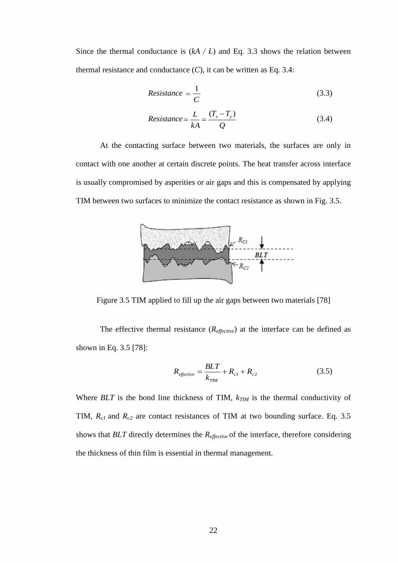
At the contacting surface between two materials, the surfaces are only in
contact with one another at certain discrete points. The heat transfer across interface
is usually compromised by asperities or air gaps and this is compensated by applying
TIM between two surfaces to minimize the contact resistance as shown in Fig. 3.5.
Figure 3.5 TIM applied to fill up the air gaps between two materials [78]
The effective thermal resistance (Reffective) at the interface can be defined as
shown in Eq. 3.5 [78]:
(3.5)
Where BLT is the bond line thickness of TIM, kTIM is the thermal conductivity of
TIM, Rc1 and Rc2 are contact resistances of TIM at two bounding surface. Eq. 3.5
shows that BLT directly determines the Reffective of the interface, therefore considering
the thickness of thin film is essential in thermal management.
Q
TT
kA
L yx )(
21 cc
TIM
effective RRk
BLTR

23
3.5 Thermal and Optical Relation in Thermal Measurements
The device junction temperature (Tj) of LEDs can be determined by:
jjj TTT 0 (3.6)
Where Tj0 is the initial LED junction temperature and ΔTj is the change in junction
temperature due to heat dissipation of LED chip. The relationship between ΔTj and
power dissipation is usually linear depends on some specific conditions, and it may
vary considerably at the extremes of LED operation. Thus, the environmental
conditions have to be considered to assure the significance of test results.
Thermal resistance (Rth) of a device is defined as the capability of the device
to transfer heat from initial point to final point. According to JEDEC standard 51-1
[79], Rth is defined as in Eq. 3.7.
H
xj
thJXP
TTR
(3.7)
Where RthJX is the thermal resistance from device junction to the specific
environment, TJ is the device junction temperature under steady state condition, TX is
the reference temperature for a specific environment or condition and PH is the
power dissipated in the device. The heat dissipation efficiency of LEDs is measured
in term of Rth and it serves to the determination of Tj that arises in the LEDs under
various operating conditions.
In the optical performance of LEDs, the light output of LEDs strongly
depends on the operating conditions. As an LED is forward biased, the input
electrical power (PI) is converted into output optical power (Popt) and power of heat
dissipation (PH) [80]. The relation is shown in terms of:
HoptI PPP (3.8)

24
At higher supplied electrical power or current, more light is generated by
LEDs. It was reported that optical efficiency achieved can up to 30% of the supplied
electrical power [81]. However, when the forward current increases, the temperature
gradient is also increases and eventually causes a drop in the light output. The
dependence of Rth with PH is redefined as in Eq. 3.9 [82]:
(3.9)
The real Rth values yield by considering the Popt in the calculations according to Eq.
3.9. The lower the Rth value, the better is the thermal performance and the device can
be protected from overheating.
optI
xj
thPP
TTR