pulsed laser deposition - semi.org semi tech event.pdf · definition pulsed laser deposition (pld)...
TRANSCRIPT

a More than Moore Deposition technology
Arjen Janssens CEO SolMateS bv
[email protected] www.solmates.nl
General introduction
Pulsed Laser Deposition

About SolMateS
1
• Paul van Attekum
SVP strategic business dev. ASML
• Rob Santilli
CEO AML Applied Microengineering Ltd.
Board of directors
• Job Elders
Senior VP Strategic Alliance
• Nard Sintenie
Partner at Twente Technology Fund
CTO
Matthijn Dekkers PhD.
CEO Arjen Janssens MSc. MBA
COO
Kristiaan Böhm MSc.
• PPM Oost
Venture capital fund 100+ investments
• Twente Technology Fund
Independent venture capital fund, specialised in
new technological developments
Investors
SolMateS
Sales Director
Jan Visser
Process R&D
Hardware R&D
Production & Service
Marketing & Sales
Strategy ,Finance,
stakeholders
• Based in Enschede Netherlands • Own demo lab cleanroom class 10000 • Access to MESA+ lab • Strong academic and prof. network • Agents in Japan, China & Korea
Definition Pulsed Laser Deposition (PLD) • PLD is a method of applying thin films to various substrates by means of an UV
Excimer laser
• PLD is somewhat similar to Sputtering except that the material plasma is generated with an excimer laser instead of accelerated ions
• Due to the ultra high energy laser spot, all target material enlightened is transformed into a plasma, achieving one-to-one transfer of target stoichiometry to substrate
• The instantaneous laser shot generates an ultra dense (super saturated) plasma with very high energy species which provides the capability to produce films that are far from the equilibrium phase
• This in combination with a reactive background gas, makes PLD very suitable for the growth of (Crystaline) Complex Metal Oxides on silicon
3
2

Experimental experience on <1” Experience on waferscale
Shortlist of Materials 3
Pulsed laser deposition has many advantages, especially for the “More than Moore” materials
4

High and stable piezo electric properties
4
5
e31 and d31 coefficients across wafer
200 nm
Cross section SEM;
High density PZT
5
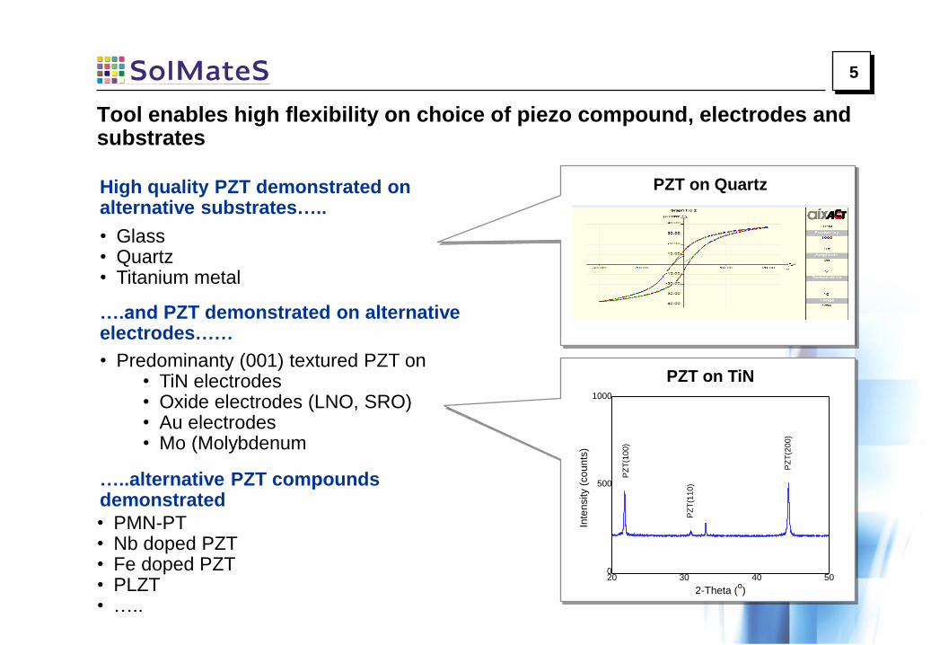
Tool enables high flexibility on choice of piezo compound, electrodes and substrates
20 30 40 500
500
1000
PZ
T(2
00
)
PZ
T(1
10
)
Inte
nsity (
co
un
ts)
2-Theta (o)
PZ
T(1
00
)
• Predominanty (001) textured PZT on • TiN electrodes • Oxide electrodes (LNO, SRO) • Au electrodes • Mo (Molybdenum
• Glass • Quartz • Titanium metal
High quality PZT demonstrated on alternative substrates…..
….and PZT demonstrated on alternative electrodes……
…..alternative PZT compounds demonstrated
• PMN-PT • Nb doped PZT • Fe doped PZT • PLZT • …..
PZT on Quartz
PZT on TiN
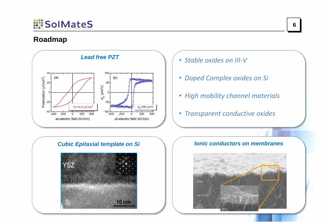
• Stable oxides on III-V
• Doped Complex oxides on Si
• High mobility channel materials
• Transparent conductive oxides
6
Roadmap
Lead free PZT
Cubic Epitaxial template on Si Ionic conductors on membranes

7
SolMateS serving world leading MEMS parties
Shipped Feb. 2013
shipped Jul 2013
See press release for more details
8