pure and cupricated basno thick film resistor: synthesis...
TRANSCRIPT

Pure and Cupricated BaSnO3 thick film resistor: Synthesis,
Characterization and studies on its gas sensing performance 1N.U. PATIL,
2V.B.GAIKWAD,
3P.D.HIRE,
3R.M.CHAUDHARI,
3M. K. DEORE,
3G. H. JAIN
*
1 Material Science Lab., K. P. G. Arts, Commerce and Sc. College, Igatpuri - 422 303, India
2 Director, BCUD University of Pune, Pune - 411 007, India
3 Material Science Lab., K. T. H. M. College, Nashik - 422 002, India
Emails :- * [email protected] & [email protected]
Submitted: Dec. 16, 2012 Accepted: Jan. 26, 2013 Published: Feb. 20, 2013
Abstract- In this work we report the synthesis, microstructure, electric properties and sensing
performance of BaSnO3 (BS) powder, it was prepared by mechano-chemical method. As prepared
powder is calcinated at temperatures 1100 oC, and 1300
oC tested for crystallization. Thick films were
prepared using simple screen-printing technology. Structural and electrical analyses were performed
and the results have been correlated. The material was tested for various gases such as CO, CO2, NH3,
Cl2, H2, LPG, ethanol, and H2S. The pure BS film shows good response multiple gases at various
operating temperature up to 5000C as NH3, CO2, CO, ethanol and, H2S for different gas concentrations,
when the pure film is surface modified with aqueous solution of Cucl2 using simple dipping technique
for various time intervals (5 min., 10 min., 20 min. and, 30 min.), film improves the selectivity and
sensitivity. Maximum response (S=36.2) was found to H2S gas at temperature of 250 0C and S=12.1 for
ethanol at 500 oC for gas concentration of 50 ppm with film dipped for 10 min. time interval. The
characterization of the films was done by XRD, SEM and TG-DTA. Crystallite size, texture coefficient,
specific surface area, electric properties and gas sensitivity of the films were measured and presented.
Index terms: BaSnO3 (BS); Thick films Resistor; H2S gas sensor; Sensitivity; Selectivity.
INTERNATIONAL JOURNAL ON SMART SENSING AND INTELLIGENT SYSTEMS VOL. 6, NO. 1, FEBRUARY 2013
433
I. INTRODUCTION
Alkaline-earth stannates (ASnO3, where A ¼ Ca, Sr, Ba) are important materials for electronic
industry due to their dielectric properties and some of their applications are thermally stable
capacitors, humidity sensors, gas sensors, etc[1-3]. The interest in perovskite-type oxides is
mainly due to the easy modification of their electric properties by the selection of an adequate
cation and also due to their stability at high temperatures [4-5]. High sensitivity semiconductor
gas sensors are strongly needed for measurement of physical quantities and for monitoring
working environments. It was discovered that atoms and molecules interacting with
semiconductor surfaces influence surface properties of semiconductors, such as conductivity and
surface potential. Semiconductor oxides have been more successfully employed as sensing
materials for the detection of different gases, such as CO, C O2, H2, alcohol, H2O, NH3, O2, NOx,
etc. The gas sensing mechanism in all polycrystalline n-type semiconductors is generally ascribed
to the Schottky barrier formation at gas-semiconductor interface, leading to a negative surface
charge accumulation, typically O− ions. The variation of the height of the inter-granular barrier is
the result of surface chemical reactions with environmental gases leading to electrical
conductance modifications [5-8].
Among all the materials used for gas sensing purposes BaSnO3 is most suitable due to its
stability, porosity and repeatability. BaSnO3 is found to be sensing many reducing gases CO,
CO2, NOx at higher temperature [9-12]. As gas sensing is a surface phenomenon we could
modify barium stannate film with some oxides so as to modify the performance [13-14]. More
specifically, we aim at better information on: (i) the effectiveness of calcination temperature on
particle size (ii) electronic properties and their changes in contact with reducing gases. Scanning
Electron microscopy (SEM), X-ray diffraction (XRD) and specific surface area measurements
were adopted to analyze the morphology, the crystalline structure and the mean grain radius.
Finally, electrical measurements (electrical properties and gas sensing properties) have been
performed.
N.U. PATIL, V.B.GAIKWAD, P.D.HIRE, R.M.CHAUDHARI, M. K. DEORE, G. H. JAIN, Pure and Cupricated BaSnO3 Thick Film Resistor: Synthesis, Characterization and Studies on its Gas Sensing Performance
434
II. EXPERIMENTAL PROCEDURE
a. Powder Preparation
The AR grade powders of Ba(OH)2.8H2O and SnO2 (with 1:1 molar concentration) were ball
milled to mix thoroughly for 2h using planetary ball mill to obtain fine grained powder. Then hot
water is added with constant stirring, followed by slow heating up to dryness. The powder was
calcinated at 1100 0C and, 1300
0C for 6h [1-6]. The fined grain powder was obtained by milling
in planetary ball mill for 2h. Powder was used to prepare thick film resistor and also for
characterization. XRD spectrum of powders were analysed and confirmed the polycrystalline
perovskite cubic phase. The as prepared powder was screen printed on glass substrate in the
desired pattern.
b. Paste and thick film preparation
The thixotropic paste was formulated by mixing the resulting fine powder BS with a temporary
binder as a mixture of organic solvents [11-13]. The ratio of the inorganic to organic part was
kept at 75:25 in formulating the paste. The thixotropic paste was then used to prepare thick films.
The paste was screen- printed on a glass substrate in a desired pattern (1.5cm x 0.5cm). The films
were fired at 600°C for 30 min. in air atmosphere to remove the residual.
c. Gas sensing system
The sensing performance of the sensors was examined using a ‘static gas sensing system’ [10-
13]. A constant D.C. voltage was applied across the film using two electrodes and current was
measured by using digital Pico-ammeter. To heat the sample up to required operating
temperatures the heater was fixed on the base plate. A thermocouple was connected to a digital
temperature indicator. A gas inlet valve was fitted at one of the ports of the base plate. The
required gas concentration inside the static system was achieved by injecting a known volume of
test gas using a gas-injecting syringe. Air was allowed to pass into the glass dome after every gas
exposure cycle.
III. MATERIAL CHARACTERISTICS
a. X-Ray Diffraction
INTERNATIONAL JOURNAL ON SMART SENSING AND INTELLIGENT SYSTEMS VOL. 6, NO. 1, FEBRUARY 2013
435
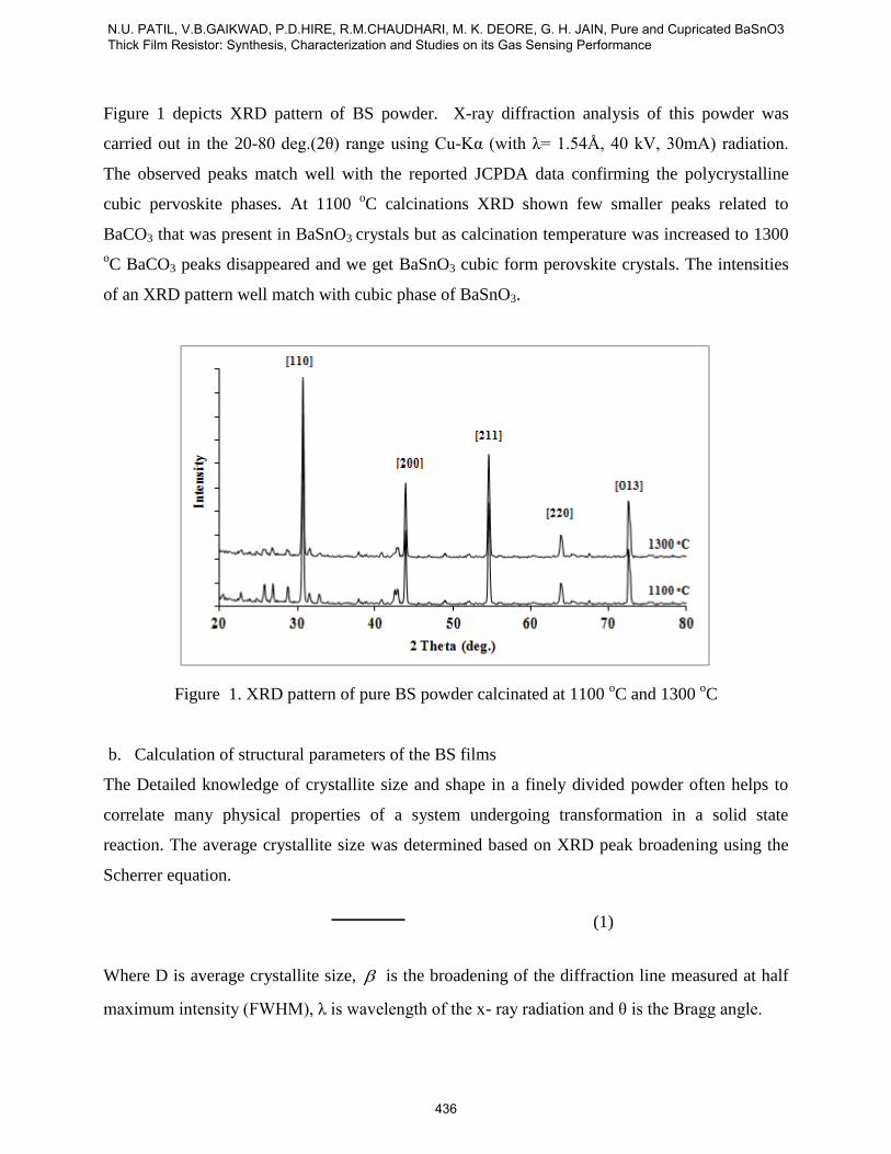
Figure 1 depicts XRD pattern of BS powder. X-ray diffraction analysis of this powder was
carried out in the 20-80 deg.(2θ) range using Cu-Kα (with λ= 1.54Å, 40 kV, 30mA) radiation.
The observed peaks match well with the reported JCPDA data confirming the polycrystalline
cubic pervoskite phases. At 1100 oC calcinations XRD shown few smaller peaks related to
BaCO3 that was present in BaSnO3 crystals but as calcination temperature was increased to 1300
oC BaCO3 peaks disappeared and we get BaSnO3 cubic form perovskite crystals. The intensities
of an XRD pattern well match with cubic phase of BaSnO3.
Figure 1. XRD pattern of pure BS powder calcinated at 1100 oC and 1300
oC
b. Calculation of structural parameters of the BS films
The Detailed knowledge of crystallite size and shape in a finely divided powder often helps to
correlate many physical properties of a system undergoing transformation in a solid state
reaction. The average crystallite size was determined based on XRD peak broadening using the
Scherrer equation.
(1)
Where D is average crystallite size, is the broadening of the diffraction line measured at half
maximum intensity (FWHM), λ is wavelength of the x- ray radiation and θ is the Bragg angle.
N.U. PATIL, V.B.GAIKWAD, P.D.HIRE, R.M.CHAUDHARI, M. K. DEORE, G. H. JAIN, Pure and Cupricated BaSnO3 Thick Film Resistor: Synthesis, Characterization and Studies on its Gas Sensing Performance
436

The specific surface area of BS thick films was calculated using BET method by using the
following equation [13]:
(2)
Where d is the diameter of the particles, ρ is the density of the particle and shape factor is 6. The
specific surface area is total surface area divided by total volume of the particles, measured in
m2/g.
c. Microstructure SEM
Figure 2 depicts the SEM images of (a) pure BS film, (b) Surface modified BS film with Copper
oxide (dipping time 05 minutes) and (c) most sensitive surface modified BS film (dipping time
10 minutes). The modified film consists of voids and a wide range of particles with particle sizes
ranging from 5 to 20 micrometer distributed non-uniformly. The surface modified film (with
dipping time of 10 min) consists of uniform smaller particles associated with larger ones. These
particles could be attributed to CuO2 particles. CuO2 grains may reside in the inter-granular
regions of BS. Thus effective surface area was expected to be increased explosively.
(a) (b)
©
INTERNATIONAL JOURNAL ON SMART SENSING AND INTELLIGENT SYSTEMS VOL. 6, NO. 1, FEBRUARY 2013
437

Figure.2.SEM images of (a) Pure BS, (b) CuO activated (05 min.) and (c) CuO activated (10
min.)
d. Elemental Analysis
The elemental composition, of Ba , Sn, , O and Cu associated in the sensor element, was carried
out using EDAX ( JEOL, JED-2300, Germany) and is represented in Table 1. Modified BS films
are observed to be more oxygen deficient than the pure BS film. This oxygen deficient would
promote the adsorption of relatively large amount of oxygen species favorable for higher gas
response. From elemental analysis (Table 1) of BS films, surface modified BS film for 10 min.
dipping time was observed to be more oxygen deficient.
Table 1. Elemental analysis of pure and surface modified BS films
Element
(Wt%)
Dipping Time in minutes
0 mim. 05 min. 10 min 15 min. 30 min.
Ba 21.78 21.95 22.81 22.37 20.47
Sn 22.54 22.61 21.92 22.51 22.01
O 55.68 55.31 54.38 55.11 55.21
Al 0.0 0.13 0.89 1.01 2.31
e. Structural Parameters and their Analysis
Table 2 shows the crystallite size, particle size and specific surface area of the samples. The grain
size is calculated using the Scherrer formula equation no (1). From XRD data of the calcinated
powders texture coefficient is calculated which shows preferential orientation of the crystal.
Specific surface area is calculated with equation no (2). The structural characteristics are
summarized in Table 2. The modified BS film with dipping time 10 minutes is characterized by
the small grain size of 29.46 nm and large active surface area (16.3 m2/g).
Table 2. Structural characteristics of pure and surface BaSn03 thick films
Sample Crystallite(Grain) Size, Particle Size, Specific Surface
N.U. PATIL, V.B.GAIKWAD, P.D.HIRE, R.M.CHAUDHARI, M. K. DEORE, G. H. JAIN, Pure and Cupricated BaSnO3 Thick Film Resistor: Synthesis, Characterization and Studies on its Gas Sensing Performance
438

D nm ( XRD) d nm (SEM) Area in m2/g
Pure 41.51 400 6.9
Mod (10min) 29.46 125 16.3
f. Thermal stability of pure and surface modified BS sample
Thermo-gravimetric analysis (TGA) of samples was carried out using Mettler Toledo Star
System - 851 from 10 to 900 0C in an air environment. The figure3 shows the TGA profiles of
pure and surface modified BS films.
Figure.3. TGA of pure and surface modified BS films
It can be concluded from the figure that the surface modified BS film was more stable than pure
BS. The weight loss in pure is more than surface modified sample for the temperature range
100OC to 400
OC and there was a continuous gain in weight of the modified BS sample after
400OC, while the weight of pure sample decreased up to 700
OC. The increase in weight of the
surface modified sample (as compared to pure BS sample) would be attributing to the adsorbed
oxygen content. The copper oxide on the surface BS sample would have formed misfit regions
between the grains of BS and could act as efficient catalysts for oxygenation.
INTERNATIONAL JOURNAL ON SMART SENSING AND INTELLIGENT SYSTEMS VOL. 6, NO. 1, FEBRUARY 2013
439

g. Thickness measurement
The thickness of the thick films was estimated by gravimetric weight loss method employing
simple formula.
(3)
In equation (3) ‘t’ is thickness of the film, ‘A’ is surface area of the film, ‘σ’ is average density of
BS, and ‘m’ is change in weight of substrate before and after deposition. The thicknesses of the
films were in the range from 65 to 90m. The reproducibility of the film thickness was achieved
by maintaining the proper rheology and thixotropy of the paste.
h. Thermoelectric power measurement
Semi-conductivity of all BS samples was confirmed by measuring thermo-electromotive force of
the BS thick film samples. It was observed to be all samples of n-type material.
IV. ELECTRICAL PROPERTIES PURE AND SURFACE MODIFIED BS THICK
FILM
a. Electrical Conductivity
Figure 4 represents the variation of conductivity with temperature of BS thick film. The
conductivity of these films goes on increasing with increase in temperature, indicating negative
temperature coefficient (NTC) of resistance. This shows the semiconducting nature of the films.
N.U. PATIL, V.B.GAIKWAD, P.D.HIRE, R.M.CHAUDHARI, M. K. DEORE, G. H. JAIN, Pure and Cupricated BaSnO3 Thick Film Resistor: Synthesis, Characterization and Studies on its Gas Sensing Performance
440
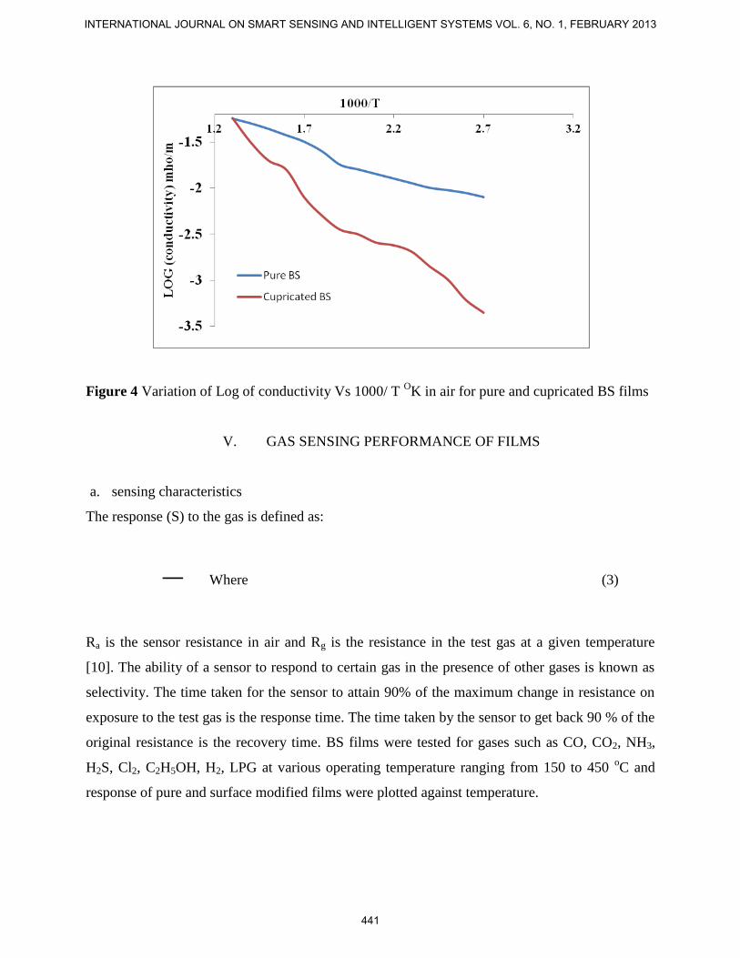
Figure 4 Variation of Log of conductivity Vs 1000/ T OK in air for pure and cupricated BS films
V. GAS SENSING PERFORMANCE OF FILMS
a. sensing characteristics
The response (S) to the gas is defined as:
Where (3)
Ra is the sensor resistance in air and Rg is the resistance in the test gas at a given temperature
[10]. The ability of a sensor to respond to certain gas in the presence of other gases is known as
selectivity. The time taken for the sensor to attain 90% of the maximum change in resistance on
exposure to the test gas is the response time. The time taken by the sensor to get back 90 % of the
original resistance is the recovery time. BS films were tested for gases such as CO, CO2, NH3,
H2S, Cl2, C2H5OH, H2, LPG at various operating temperature ranging from 150 to 450 oC and
response of pure and surface modified films were plotted against temperature.
INTERNATIONAL JOURNAL ON SMART SENSING AND INTELLIGENT SYSTEMS VOL. 6, NO. 1, FEBRUARY 2013
441
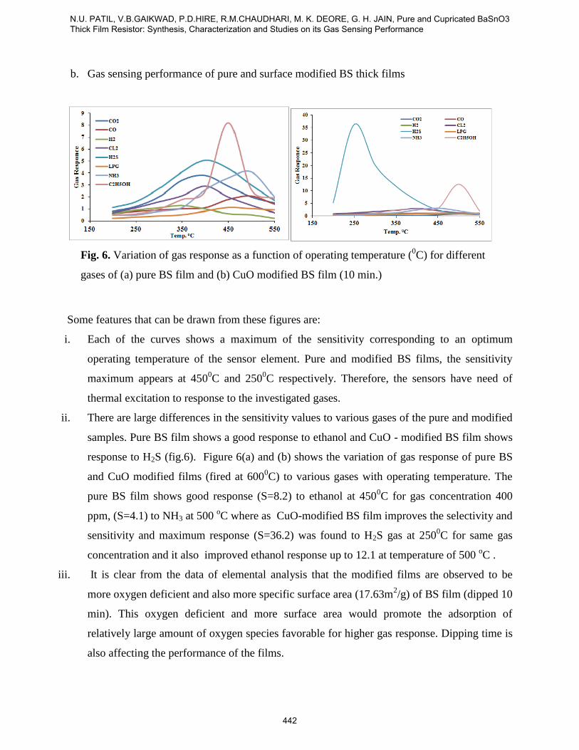
b. Gas sensing performance of pure and surface modified BS thick films
Fig. 6. Variation of gas response as a function of operating temperature (0C) for different
gases of (a) pure BS film and (b) CuO modified BS film (10 min.)
Some features that can be drawn from these figures are:
i. Each of the curves shows a maximum of the sensitivity corresponding to an optimum
operating temperature of the sensor element. Pure and modified BS films, the sensitivity
maximum appears at 4500C and 250
0C respectively. Therefore, the sensors have need of
thermal excitation to response to the investigated gases.
ii. There are large differences in the sensitivity values to various gases of the pure and modified
samples. Pure BS film shows a good response to ethanol and CuO - modified BS film shows
response to H2S (fig.6). Figure 6(a) and (b) shows the variation of gas response of pure BS
and CuO modified films (fired at 6000C) to various gases with operating temperature. The
pure BS film shows good response (S=8.2) to ethanol at 4500C for gas concentration 400
ppm, (S=4.1) to NH3 at 500 oC where as CuO-modified BS film improves the selectivity and
sensitivity and maximum response (S=36.2) was found to H2S gas at 2500C for same gas
concentration and it also improved ethanol response up to 12.1 at temperature of 500 oC .
iii. It is clear from the data of elemental analysis that the modified films are observed to be
more oxygen deficient and also more specific surface area (17.63m2/g) of BS film (dipped 10
min). This oxygen deficient and more surface area would promote the adsorption of
relatively large amount of oxygen species favorable for higher gas response. Dipping time is
also affecting the performance of the films.
N.U. PATIL, V.B.GAIKWAD, P.D.HIRE, R.M.CHAUDHARI, M. K. DEORE, G. H. JAIN, Pure and Cupricated BaSnO3 Thick Film Resistor: Synthesis, Characterization and Studies on its Gas Sensing Performance
442

c. Variation of Sensitivity with dipping time
Fig. 7. Variation in gas response to H2S with dipping
d. Response and Recovery of pure and cupricated BS film to various gases
Response time (RST) is defined as the time required for sensor to attain the 90% of the maximum
change in the conductance after exposure to the target gas on the surface of the film, while
recovery time (RCT) is the time taken to get back 90 % of the initial value of the conductance
once gas is made off. It was observed that RST is slightly higher for pure BS but when film is
cupricated RST is improved. Similarly it was observed that RCT was increased in cupricated
films.
Fig. 8. Response and Recovery time for pure BS and CuO-BS film for H2S gas
INTERNATIONAL JOURNAL ON SMART SENSING AND INTELLIGENT SYSTEMS VOL. 6, NO. 1, FEBRUARY 2013
443

VI. DISCUSSION
The gas sensing mechanism belongs to the surface controlled type which is based on the change
of the electrical conductance of the semiconducting material upon exposure to different gases.
The gas sensitivity is a function of grain size, surface state and oxygen adsorption. The surface
modified films can be looked upon as the small particles of aluminum oxide distributed along the
grain boundaries of BS. The H2S gas is reducing in nature. On exposure of H2S gas on the surface
modified BS film, the sensor resistance decreases suddenly giving higher sensitivity. It can
reduce Al2O3 into Al2S3 which are metallic in nature and is more conducting. This can be
represented as:
CuO + H2S CuS + H2O (1)
Upon subsequent exposure of sensor to air ambient at elevated temperature, sulphides got
oxidized and could be recovered back to oxides as
CuS + 2O2 CuO + SO3 (2)
When oxygen is adsorbed on the surface of BS, abstracting electrons, and thus an increase in
potential barrier at the grain boundaries. When reducing gas such as H2S is adsorbed between the
grains of BS, the potential barrier decreases as a result of oxidative conversion of the H2S gas.
H2S reacts with adsorbed oxygen ions as:
2 H2S + 3O- 2 H2O +2 SO2 + 6 e
- (3)
With this reaction, many electrons could release to thick film surface. This could make the
Schottky surface barrier decrease; with the depletion layer thinner; consequently, the electrical
conductance of the thin film increases. More gas would be adsorbed by the thin film surface;
consequently, the gas sensitivity was enhanced. Increase in operating temperature causes
oxidation of large number of H2S molecules, thus producing very large number of electrons.
Therefore, conductivity increases to a large extent. This is the reason why the gas sensitivity
N.U. PATIL, V.B.GAIKWAD, P.D.HIRE, R.M.CHAUDHARI, M. K. DEORE, G. H. JAIN, Pure and Cupricated BaSnO3 Thick Film Resistor: Synthesis, Characterization and Studies on its Gas Sensing Performance
444

increases with operating temperature. However, the sensitivity decreases at higher operating
temperature, as the oxygen adsorbates are desorbed from the surface of the sensor. Also, at higher
temperature, the carrier concentration increases due to intrinsic thermal excitation and the Debye
length decreases. This may be one of the reasons for decreased gas sensitivity at higher
temperature.
VII. SUMMARY AND CONCLUSIONS
The sensing mechanism of the BS was the “surface-controlled gas-sensing mechanism-
(adsorption - desorption of oxygen)”. Barium stannet was prepared by solid state reaction
(mechano-chemical) chemical method. Pure BS film has a good response to ethanol and NH3 gas
and CuO-modified BS film has a good response to H2S gas at optimum working temperature of
5000C and 250
0C respectively. Modified film was selective and sensitive to H2S gas; it can be
due to fact that the film has maximum active surface area and smallest grain size as compared to
pure film. The pure BS film shows good response (S=8.2) to ethanol and NH3 at 5000C for gas
concentration 50 ppm and CuO-modified BS film improves the selectivity and sensitivity and
maximum response (S=36.2) was found to H2S gas at 2500C and improvement for ethanol to 12.1
at 500 oC for same and or even smaller gas concentrations up to 50 ppm. It is clear from the data
of elemental analysis that the modified BS film is observed to be more oxygen deficient, smaller
grain size and more specific surface area ( m2/g). This film could be more selective and sensitive
to H2S.
REFERENCES
[01] H Sano, R. H. Herber, Moessbauer, “parameters of Barium Stannate”, Journal Inorg.
Nucl. Chem. 30(1988)2, 409-413
[02] T. R. N. Kutty and , R. Vivekanandan, “Synthesis of BaSnO3 using hydrothermal
method” Mat. Res. Bull., 22(1987)11, 1457-1465
[03] W. Lu, , H Schmitt, “preparation and characterization of BaSnO3 powders by
hydrothermal synthesis from tin oxide hydrate gel”, J of materials science 42(2007)1007-1013
[04] W. Lu, H Schmitt, “Synthesis of nano-sized BaSnO3powders from metal iso-propoxides”,
J. Sol-gel sc. Techn. 42(2007); 55-64.
INTERNATIONAL JOURNAL ON SMART SENSING AND INTELLIGENT SYSTEMS VOL. 6, NO. 1, FEBRUARY 2013
445
[05] C. P. Udawatte, M Yoshimura, “preparation of well crystalline BaSnO3 powders under
hydrothermal conditions” , Materials Letters 47(2001)7-10
[06] G. H. Jain, V. B. Gaikwad, L. A.Patil, “Studies on gas sensing performance of
(Ba0.8Sr0.2)(Sn0.8Ti0.2)O3 thick film resistors”, Sens. . Actuators, B, 122, 2007, pp. 605-612.
[07] A.M. Azad, S.A. Akbar, S.G. Mhaisalkar, L.D. Birkefeld, K.S. Goto, “Solid-state gas
sensors: a review”, J. Electro-chem. Soc. 122, 1992, pp. 3690–3703.
[08] C.A.Harper, Hand book of thick film hybrid Microelectronics, McGraw Hill Book Co.,
New York, 1974.
[09] Zhang, K. Colbow, “Surface silver clusters as oxidation catalysts on semiconductor gas
sensors”, Sensors and Actuators , B, 40,1997,pp. 47–52.
[10] G. H. Jain, V. B. Gaikwad, L. A. Patil, “Studies on gas sensing performance of
(Ba0.8Sr0.2)(Sn0.8Ti0.2)O3 thick film resistors”, Sens. . Actuators, B, 122, 2007, pp. 605-612.
[11] S. A. Patil, L.A.Patil, D.R. Patil, G. H. Jain, M. S. Wagh, “CuO-modified tin titanate thick
film resistors as H2-gas sensors”, Sensors and Actuators B, 123 ,2007,pp. 233-239.
[12] G. E. Patil and G. H. Jain, “Nanocrystalline CdSnO3 thin film as highly sensitive ethanol
sensor”, Proceedings of 5th International Conference on Sensing Technology ICST-2011, 978-
1-4577-0168-9, pp. 249–252, DOI. 10.1109 / ICSensT. 2011. 6136975, 2012.
[13] A. Rothschild and Y. Komen, “The effect of grain size on the sensitivity of nano-
crystalline metal-oxide gas sensors” J. Appl. Phys. Vol. 95, No. 11, 2004, pp. 6374-6380.
[14] N. Yamazoe, G. Sakai, K. Shimanoe, “Oxide semiconductor gas sensors”, Catal. Surv.
Asia Vol. 7 2003, pp. 63–75
[15] Z. Gergintschew, H. Förster, J. Kositza, D. Schipanski, “Two-dimensional numerical
simulation of semiconductor gas sensors”, Sens. Actuators B, Vol. 26, 1995, pp.170–173.
[16] L. A. Patil, M. D. Shinde, A. R. Bari, V. V. Deo, D. M. Patil, M. P. Kaushik, “Fe2O3
modified thick films of nanostructured SnO2 powder consisting of hollow microspheres
synthesized from pyrolysis of ultrasonically atomized aerosol for LPG sensing”, Sensors and
Actuators B 155 (2011) 174–182.
[17] G. E Patil, D. D. Kajale, V. B. Gaikwad and G. H. Jain, “Nano-crystalline Tin Oxide Thin
Film as a Low Level H2S Gas Sensor”, International Journal of Nano-science, Vol. 10, No. 4,
2011, pp. 1-5.
[18] N. K. Pawar and G. H. Jain, Proceedings of 5th International Conference on Sensing
N.U. PATIL, V.B.GAIKWAD, P.D.HIRE, R.M.CHAUDHARI, M. K. DEORE, G. H. JAIN, Pure and Cupricated BaSnO3 Thick Film Resistor: Synthesis, Characterization and Studies on its Gas Sensing Performance
446
Technology, ICST 2011, “Study of nano Fe2O3 MOS thick films as ethanol gas sensor”, (2011),
pp. 121-124.
[19] S. D. Shinde, G. E. Patil, D. D. Kajale, V. B. Gaikwad and G. H. Jain, “Synthesis of ZnO
nano-rods by hydrothermal method for gas sensor applications”, International Journal on Smart
Sensing and Intelligent System, Vol. 5, No. 1, March 2012, pp. 57-70.
[20] N. K. Pawar, D. D. Kajale, G. E. Patil, V. G. Wagh, V. B. Gaikwad , M. K. Deore and G.
H. Jain “Nano-structured Fe2O3 Thick Film as an Ethanol Sensor” International Journal on
Smart Sensing and Intelligent System, Vol. 5, No. 2, June 2012, pp. 447-70. 457
[21] S. D. Shinde, G. E. Patil, D. D. Kajale, V. G. Wagh, V. B. Gaikwad and G. H. Jain, “Effect
of annealing on gas sensing performance of nano-structured ZnO thick film resistors”,
International Journal on Smart Sensing and Intelligent System, Vol. 5, No. 1, March 2012, pp.
277-294.
[22] Ganesh E. Patil D. D. Kajale, P. T. Ahire, D. N. Chavan, N. K. Pawar, S. D. Shinde, V. B.
Gaikwad, G. H. Jain, “Synthesis, characterization and gas sensing performance of SnO2 thin
films prepared by spray pyrolysis”, Bulletin of Material Science Vol. 34, No. 1, 2011, pp. 1–9.
[23] S. D. Shinde, G. E. Patil, D. D. Kajale, V. B. Gaikwad and G. H. Jain, “Synthesis of ZnO
nano-rods by spray pyrolysis for H2S gas sensor”, Journal of Alloys and Compounds, Vol. 528,
2012, pp. 109-114.
[24] Ganesh E. Patil, D. D. Kajale, V. B. Gaikwad, N. K. Pawar and G. H. Jain, “Properties and
Gas Sensing Mechanism Study of CTO Thin Films as Ethanol Sensor”, Sensors & Transducers
Journal, Vol. 137, Issue 2, February 2012, pp. 47-58.
[25] Ganesh E. Patil and G. H. Jain, “Nano-crystalline CdSnO3 thin film as highly sensitive
ethanol sensor”, Proceedings of 5th International Conference on Sensing Technology ICST-
2011, 978-1-4577-0168-9, pp. 249–252.
INTERNATIONAL JOURNAL ON SMART SENSING AND INTELLIGENT SYSTEMS VOL. 6, NO. 1, FEBRUARY 2013
447