qt2022/32 - data sheet: ds3051
TRANSCRIPT

QT2022/32 - Data Sheet: DS305110 Gb/s Serial-to-XAUI PHY ICs for Ethernet and Fibre Channel LAN/
SAN/WAN Applications (CDR)April 7, 2010
1 DescriptionThe QT2032 and QT2022 products are fully integrated PHY ICs designed for use in 10 Gb/s IEEE 802.3-2005 compliant Ethernet and Fibre Channel LAN, SAN and WAN applications. The main physical layer functions (PHY) of the receiver and transmitter are integrated onto a single chip. The QT2022 is a serial to XAUI bidirectional PHY chip that integrates the XGXS, PCS and PMA layers and sup-ports 10 Gb/s Ethernet (10GBASE-R) and 10 Gb/s Fibre Channel protocols. In addition to the QT2022 features, the QT2032 includes an IEEE802.3-2005 WAN Interface Sublayer (WIS) for Ethernet over SONET protocol (10GBASE-W). This layer can be bypassed for LAN or SAN applications.In the transmit direction, the chip converts four differential input 3.125 Gb/s lanes (XAUI) into a serial 9.95-10.5 Gb/s data stream. In the receive direction the chip converts an input serial 9.95-10.5 Gb/s data stream into four differ-ential output 3.125 Gb/s lanes (XAUI). The QT2032 and QT2022 include a standard two-wire interface for communicating with external EEPROM and DOM devices or XFP modules. An MDC/MDIO interface provides control and status capability for the IC.In the QT2032, maximum flexibility is provided by the transmit data clocking and jitter clean-up options and extended SONET overhead processing when connecting the module to the existing OC-192 and DWDM networks. The QT2032 and QT2022 are fully compliant with IEEE 802.3-2005 10GE and ANSI INCITS/T11 10GFC stan-dards, and the XENPAK, XPAK, X2, and XFP Multi Source Agreements (MSA).
2 Applications10 Gb/s Ethernet and Fibre Channel LAN, SAN and WAN applications. XENPAK, XPAK, and X2 fiber optic mod-ules. System cards that support XFP modules.
Figure 1: Application Diagrams for QT2032 and QT2022. Top: System application. Bottom: Module application.
LAYER 2/3/4Switch ASIC
QT2032/QT2022
QT2032/QT2022
LaserDriver
OpticsXAUI XFI
MDIO I2C
TIA
EEPROM
Integrated Optical TransceiverEthernet Switch
LAYER 2/3/4Switch ASIC
QT2032/QT2022
QT2032/QT2022
LaserDriver
OpticsXAUI XFI
MDIO I2C
TIA
EEPROM
Integrated Optical TransceiverEthernet Switch
SWITCH/NETWORK
PROCESSORMAC QT2032/
QT2022QT2032/QT2022 OpticsXAUI XFI
XFP Module
MDIOI2C
SWITCH/NETWORK
PROCESSORMAC QT2032/
QT2022QT2032/QT2022 OpticsXAUI XFI
XFP Module
MDIOI2C
Revision 5.11 AppliedMicro - Confidential & Proprietary 1

QT2022/32 - Data Sheet: DS3051
TABLE OF CONTENTS1 Description . . . . . . . . . . . . . . . . . . . . . . . . . . . . . . . . . . . . . . . . . . . . . . . . . . . . . . . . . . . . . . . . . . . . . . . . . . . . . . 12 Applications. . . . . . . . . . . . . . . . . . . . . . . . . . . . . . . . . . . . . . . . . . . . . . . . . . . . . . . . . . . . . . . . . . . . . . . . . . . . . . 13 Available Package Options . . . . . . . . . . . . . . . . . . . . . . . . . . . . . . . . . . . . . . . . . . . . . . . . . . . . . . . . . . . . . . . . . 104 Pin Assignment and Description . . . . . . . . . . . . . . . . . . . . . . . . . . . . . . . . . . . . . . . . . . . . . . . . . . . . . . . . . . . . . 11
4.1 QT2032 Ball Arrangement . . . . . . . . . . . . . . . . . . . . . . . . . . . . . . . . . . . . . . . . . . . . . . . . . . . . . . . . . . . . . 114.2 QT2022 Ball Arrangement . . . . . . . . . . . . . . . . . . . . . . . . . . . . . . . . . . . . . . . . . . . . . . . . . . . . . . . . . . . . . 12
5 Datapath Description . . . . . . . . . . . . . . . . . . . . . . . . . . . . . . . . . . . . . . . . . . . . . . . . . . . . . . . . . . . . . . . . . . . . . 215.1 Transmit Path . . . . . . . . . . . . . . . . . . . . . . . . . . . . . . . . . . . . . . . . . . . . . . . . . . . . . . . . . . . . . . . . . . . . . . . 215.2 Receive Path . . . . . . . . . . . . . . . . . . . . . . . . . . . . . . . . . . . . . . . . . . . . . . . . . . . . . . . . . . . . . . . . . . . . . . . 24
6 Datapath Clocking. . . . . . . . . . . . . . . . . . . . . . . . . . . . . . . . . . . . . . . . . . . . . . . . . . . . . . . . . . . . . . . . . . . . . . . . 266.1 LAN Application Timing Modes (QT2022 and QT2032) . . . . . . . . . . . . . . . . . . . . . . . . . . . . . . . . . . . . . . . 266.2 WAN Application Timing Modes (QT2032 Only). . . . . . . . . . . . . . . . . . . . . . . . . . . . . . . . . . . . . . . . . . . . . 276.3 TXPLLOUT Output Clock Driver . . . . . . . . . . . . . . . . . . . . . . . . . . . . . . . . . . . . . . . . . . . . . . . . . . . . . . . . . 35
7 WAN Interface Sublayer (WIS) Description (QT2032 Only) . . . . . . . . . . . . . . . . . . . . . . . . . . . . . . . . . . . . . . . . 367.1 WIS Transmitter . . . . . . . . . . . . . . . . . . . . . . . . . . . . . . . . . . . . . . . . . . . . . . . . . . . . . . . . . . . . . . . . . . . . . 367.2 WIS Receiver . . . . . . . . . . . . . . . . . . . . . . . . . . . . . . . . . . . . . . . . . . . . . . . . . . . . . . . . . . . . . . . . . . . . . . . 407.3 Extended WIS Features . . . . . . . . . . . . . . . . . . . . . . . . . . . . . . . . . . . . . . . . . . . . . . . . . . . . . . . . . . . . . . . 467.4 WIS Alarm Processing . . . . . . . . . . . . . . . . . . . . . . . . . . . . . . . . . . . . . . . . . . . . . . . . . . . . . . . . . . . . . . . . 52
8 Control and Status Pins Detailed Description . . . . . . . . . . . . . . . . . . . . . . . . . . . . . . . . . . . . . . . . . . . . . . . . . . . 548.1 General Notes. . . . . . . . . . . . . . . . . . . . . . . . . . . . . . . . . . . . . . . . . . . . . . . . . . . . . . . . . . . . . . . . . . . . . . . 548.2 Control (Input) Pins (QT2022 and QT2032). . . . . . . . . . . . . . . . . . . . . . . . . . . . . . . . . . . . . . . . . . . . . . . . 548.3 Control (Input) Pins (QT2032 only) . . . . . . . . . . . . . . . . . . . . . . . . . . . . . . . . . . . . . . . . . . . . . . . . . . . . . . 598.4 Low-Speed Output Pins (QT2022 and QT2032). . . . . . . . . . . . . . . . . . . . . . . . . . . . . . . . . . . . . . . . . . . . . 618.5 Low-Speed Output Pins (QT2032 only) . . . . . . . . . . . . . . . . . . . . . . . . . . . . . . . . . . . . . . . . . . . . . . . . . . . 708.6 LED/GPIO Driver Pins (LEDx) . . . . . . . . . . . . . . . . . . . . . . . . . . . . . . . . . . . . . . . . . . . . . . . . . . . . . . . . . . 708.7 Analog Control Pins . . . . . . . . . . . . . . . . . . . . . . . . . . . . . . . . . . . . . . . . . . . . . . . . . . . . . . . . . . . . . . . . . . 72
9 MDIO Interface . . . . . . . . . . . . . . . . . . . . . . . . . . . . . . . . . . . . . . . . . . . . . . . . . . . . . . . . . . . . . . . . . . . . . . . . . . 739.1 Management Data Clock (MDC). . . . . . . . . . . . . . . . . . . . . . . . . . . . . . . . . . . . . . . . . . . . . . . . . . . . . . . . . 739.2 Management Data I/O (MDIO) . . . . . . . . . . . . . . . . . . . . . . . . . . . . . . . . . . . . . . . . . . . . . . . . . . . . . . . . . . 739.3 MDIO Timing Relationship to MDC. . . . . . . . . . . . . . . . . . . . . . . . . . . . . . . . . . . . . . . . . . . . . . . . . . . . . . . 739.4 MDIO Bus Initialization . . . . . . . . . . . . . . . . . . . . . . . . . . . . . . . . . . . . . . . . . . . . . . . . . . . . . . . . . . . . . . . . 749.5 MDIO Pin . . . . . . . . . . . . . . . . . . . . . . . . . . . . . . . . . . . . . . . . . . . . . . . . . . . . . . . . . . . . . . . . . . . . . . . . . . 749.6 Management Frame Format . . . . . . . . . . . . . . . . . . . . . . . . . . . . . . . . . . . . . . . . . . . . . . . . . . . . . . . . . . . . 749.7 XFP Module Access Through MDIO. . . . . . . . . . . . . . . . . . . . . . . . . . . . . . . . . . . . . . . . . . . . . . . . . . . . . . 77
10 Two Wire (EEPROM) Interface. . . . . . . . . . . . . . . . . . . . . . . . . . . . . . . . . . . . . . . . . . . . . . . . . . . . . . . . . . . . . 7910.1 EEPROM Data Transfer Timing . . . . . . . . . . . . . . . . . . . . . . . . . . . . . . . . . . . . . . . . . . . . . . . . . . . . . . . . 8110.2 EEPROM 256 Byte Read Cycle . . . . . . . . . . . . . . . . . . . . . . . . . . . . . . . . . . . . . . . . . . . . . . . . . . . . . . . . 8210.3 EEPROM 256 Byte Write Cycle . . . . . . . . . . . . . . . . . . . . . . . . . . . . . . . . . . . . . . . . . . . . . . . . . . . . . . . . 8310.4 EEPROM Single Byte Read or Write Cycle . . . . . . . . . . . . . . . . . . . . . . . . . . . . . . . . . . . . . . . . . . . . . . . 8410.5 XENPAK Diagnostic Optical Monitoring (DOM) . . . . . . . . . . . . . . . . . . . . . . . . . . . . . . . . . . . . . . . . . . . . 8410.6 Two-byte Addressing of Peripheral I2C Devices . . . . . . . . . . . . . . . . . . . . . . . . . . . . . . . . . . . . . . . . . . . 8910.7 Register Configuration from External EEPROM . . . . . . . . . . . . . . . . . . . . . . . . . . . . . . . . . . . . . . . . . . . . 9110.8 I2C Slave Mode for Register Configuration . . . . . . . . . . . . . . . . . . . . . . . . . . . . . . . . . . . . . . . . . . . . . . . 93
11 Diagnostic and Test Features . . . . . . . . . . . . . . . . . . . . . . . . . . . . . . . . . . . . . . . . . . . . . . . . . . . . . . . . . . . . . . 9611.1 Loopback Modes . . . . . . . . . . . . . . . . . . . . . . . . . . . . . . . . . . . . . . . . . . . . . . . . . . . . . . . . . . . . . . . . . . . 9611.2 XAUI Interface Test Features . . . . . . . . . . . . . . . . . . . . . . . . . . . . . . . . . . . . . . . . . . . . . . . . . . . . . . . . . . 9811.3 PCS Test Features . . . . . . . . . . . . . . . . . . . . . . . . . . . . . . . . . . . . . . . . . . . . . . . . . . . . . . . . . . . . . . . . . . 9911.4 Serial Interface Test Features. . . . . . . . . . . . . . . . . . . . . . . . . . . . . . . . . . . . . . . . . . . . . . . . . . . . . . . . . 10011.5 WIS Test Features (QT2032 only) . . . . . . . . . . . . . . . . . . . . . . . . . . . . . . . . . . . . . . . . . . . . . . . . . . . . . 10211.6 Ethernet Packet Generator/Checker (QT2032 and QT2022) . . . . . . . . . . . . . . . . . . . . . . . . . . . . . . . . . 10311.7 Disabling the Idle Decode Process. . . . . . . . . . . . . . . . . . . . . . . . . . . . . . . . . . . . . . . . . . . . . . . . . . . . . 106
2 AppliedMicro - Confidential & Proprietary Revision 5.11

QT2022/32 - Data Sheet: DS3051
11.8 Test Access Port and Boundary Scan . . . . . . . . . . . . . . . . . . . . . . . . . . . . . . . . . . . . . . . . . . . . . . . . . . 10612 Extended Link Monitoring Feature (QT2032 and QT2022). . . . . . . . . . . . . . . . . . . . . . . . . . . . . . . . . . . . . . . 109
12.1 Overview. . . . . . . . . . . . . . . . . . . . . . . . . . . . . . . . . . . . . . . . . . . . . . . . . . . . . . . . . . . . . . . . . . . . . . . . . 10912.2 Query message format . . . . . . . . . . . . . . . . . . . . . . . . . . . . . . . . . . . . . . . . . . . . . . . . . . . . . . . . . . . . . . 11012.3 Messaging . . . . . . . . . . . . . . . . . . . . . . . . . . . . . . . . . . . . . . . . . . . . . . . . . . . . . . . . . . . . . . . . . . . . . . . 11012.4 Extended Link Monitoring State Diagram . . . . . . . . . . . . . . . . . . . . . . . . . . . . . . . . . . . . . . . . . . . . . . . . 11112.5 Transmit State Diagram . . . . . . . . . . . . . . . . . . . . . . . . . . . . . . . . . . . . . . . . . . . . . . . . . . . . . . . . . . . . . 11212.6 Receive State Diagram. . . . . . . . . . . . . . . . . . . . . . . . . . . . . . . . . . . . . . . . . . . . . . . . . . . . . . . . . . . . . . 11312.7 RMDIO (Remote MDIO Access) Extended Link Monitoring . . . . . . . . . . . . . . . . . . . . . . . . . . . . . . . . . . 11312.8 PRBS Performance Monitoring. . . . . . . . . . . . . . . . . . . . . . . . . . . . . . . . . . . . . . . . . . . . . . . . . . . . . . . . 115
13 QT2022/32 MII Register Map . . . . . . . . . . . . . . . . . . . . . . . . . . . . . . . . . . . . . . . . . . . . . . . . . . . . . . . . . . . . . 11713.1 PMA/PMD Internal Control Registers (Device 1) . . . . . . . . . . . . . . . . . . . . . . . . . . . . . . . . . . . . . . . . . . 11813.2 WIS Registers (Device 2) (QT2032 only) . . . . . . . . . . . . . . . . . . . . . . . . . . . . . . . . . . . . . . . . . . . . . . . . 14113.3 PCS Registers (Device 3) . . . . . . . . . . . . . . . . . . . . . . . . . . . . . . . . . . . . . . . . . . . . . . . . . . . . . . . . . . . . 16413.4 PHY_XS Registers (Device 4) . . . . . . . . . . . . . . . . . . . . . . . . . . . . . . . . . . . . . . . . . . . . . . . . . . . . . . . . 175
14 AC and DC Parameters . . . . . . . . . . . . . . . . . . . . . . . . . . . . . . . . . . . . . . . . . . . . . . . . . . . . . . . . . . . . . . . . . 18615 Mechanical . . . . . . . . . . . . . . . . . . . . . . . . . . . . . . . . . . . . . . . . . . . . . . . . . . . . . . . . . . . . . . . . . . . . . . . . . . . 203
15.1 PCB Layout Recommendations . . . . . . . . . . . . . . . . . . . . . . . . . . . . . . . . . . . . . . . . . . . . . . . . . . . . . . . 20515.2 Baking instructions . . . . . . . . . . . . . . . . . . . . . . . . . . . . . . . . . . . . . . . . . . . . . . . . . . . . . . . . . . . . . . . . . 20515.3 Thermal Reflow Profile . . . . . . . . . . . . . . . . . . . . . . . . . . . . . . . . . . . . . . . . . . . . . . . . . . . . . . . . . . . . . . 205
16 Marking Drawing . . . . . . . . . . . . . . . . . . . . . . . . . . . . . . . . . . . . . . . . . . . . . . . . . . . . . . . . . . . . . . . . . . . . . . . 20717 Thermal . . . . . . . . . . . . . . . . . . . . . . . . . . . . . . . . . . . . . . . . . . . . . . . . . . . . . . . . . . . . . . . . . . . . . . . . . . . . . . 20818 Application Notes . . . . . . . . . . . . . . . . . . . . . . . . . . . . . . . . . . . . . . . . . . . . . . . . . . . . . . . . . . . . . . . . . . . . . . 209
18.1 External Components . . . . . . . . . . . . . . . . . . . . . . . . . . . . . . . . . . . . . . . . . . . . . . . . . . . . . . . . . . . . . . . 20918.2 Loop Filter Component Selection . . . . . . . . . . . . . . . . . . . . . . . . . . . . . . . . . . . . . . . . . . . . . . . . . . . . . . 21018.3 Power Supply Filtering and Decoupling . . . . . . . . . . . . . . . . . . . . . . . . . . . . . . . . . . . . . . . . . . . . . . . . . 21018.4 Dual 10GE & 10GFC Rate Support . . . . . . . . . . . . . . . . . . . . . . . . . . . . . . . . . . . . . . . . . . . . . . . . . . . . 21018.5 Reset Requirements . . . . . . . . . . . . . . . . . . . . . . . . . . . . . . . . . . . . . . . . . . . . . . . . . . . . . . . . . . . . . . . . 21018.6 MDIO Bus Implementation . . . . . . . . . . . . . . . . . . . . . . . . . . . . . . . . . . . . . . . . . . . . . . . . . . . . . . . . . . . 21318.7 Improving MDIO Bus Integrity. . . . . . . . . . . . . . . . . . . . . . . . . . . . . . . . . . . . . . . . . . . . . . . . . . . . . . . . . 21418.8 XAUI Traffic Testing with a BERT. . . . . . . . . . . . . . . . . . . . . . . . . . . . . . . . . . . . . . . . . . . . . . . . . . . . . . 21518.9 Jumbo Frame Support and Round-Trip Delay in WAN Applications . . . . . . . . . . . . . . . . . . . . . . . . . . . 21618.10 DOM Memory Behavior . . . . . . . . . . . . . . . . . . . . . . . . . . . . . . . . . . . . . . . . . . . . . . . . . . . . . . . . . . . . 216
19 References . . . . . . . . . . . . . . . . . . . . . . . . . . . . . . . . . . . . . . . . . . . . . . . . . . . . . . . . . . . . . . . . . . . . . . . . . . . 21720 Ordering Information . . . . . . . . . . . . . . . . . . . . . . . . . . . . . . . . . . . . . . . . . . . . . . . . . . . . . . . . . . . . . . . . . . . . 219
Revision 5.11 AppliedMicro - Confidential & Proprietary 3
QT2022/32 - Data Sheet: DS3051
LIST OF FIGURESFigure 1: Application Diagrams for QT2032 and QT2022. Top: System application. Bottom: Module application.. . . . . . . . . . . . . . . . . . . . . . . . . . . . . . . . . . . . . . . . . . . . . . . . . . . . . . . . . . . . . . . . . . . 1Figure 2: QT2022/32 Functional Block Diagram . . . . . . . . . . . . . . . . . . . . . . . . . . . . . . . . . . . . . . . . . . . . . . . . . . 21Figure 3: Transmit Scrambler. . . . . . . . . . . . . . . . . . . . . . . . . . . . . . . . . . . . . . . . . . . . . . . . . . . . . . . . . . . . . . . . . 23Figure 4: Receive Descrambler . . . . . . . . . . . . . . . . . . . . . . . . . . . . . . . . . . . . . . . . . . . . . . . . . . . . . . . . . . . . . . . 25Figure 5: LAN Mode Timing (QT2022 and QT2032) . . . . . . . . . . . . . . . . . . . . . . . . . . . . . . . . . . . . . . . . . . . . . . . 26Figure 6: WAN Mode Timing with Fixed Frequency Reference . . . . . . . . . . . . . . . . . . . . . . . . . . . . . . . . . . . . . . . 28Figure 7: WAN Mode Timing without Fixed Frequency Reference . . . . . . . . . . . . . . . . . . . . . . . . . . . . . . . . . . . . 29Figure 8: Line Timing Enable Logic . . . . . . . . . . . . . . . . . . . . . . . . . . . . . . . . . . . . . . . . . . . . . . . . . . . . . . . . . . . . 31Figure 9: VCXO PLL Interface Block Diagram. . . . . . . . . . . . . . . . . . . . . . . . . . . . . . . . . . . . . . . . . . . . . . . . . . . . 33Figure 10: WIS Frame Structure . . . . . . . . . . . . . . . . . . . . . . . . . . . . . . . . . . . . . . . . . . . . . . . . . . . . . . . . . . . . . . 36Figure 11: WIS Receive Interface Process . . . . . . . . . . . . . . . . . . . . . . . . . . . . . . . . . . . . . . . . . . . . . . . . . . . . . . 40Figure 12: STS-1 Payload pointer (H1, H2, H3) coding. . . . . . . . . . . . . . . . . . . . . . . . . . . . . . . . . . . . . . . . . . . . . 43Figure 13: Receive Bit Relabelling Function . . . . . . . . . . . . . . . . . . . . . . . . . . . . . . . . . . . . . . . . . . . . . . . . . . . . . 46Figure 14: Serial Overhead Interface Timing Diagram. . . . . . . . . . . . . . . . . . . . . . . . . . . . . . . . . . . . . . . . . . . . . . 49Figure 15: TX WIS Overhead Insertion Control Register . . . . . . . . . . . . . . . . . . . . . . . . . . . . . . . . . . . . . . . . . . . . 50Figure 16: Open Drain Driver Configuration . . . . . . . . . . . . . . . . . . . . . . . . . . . . . . . . . . . . . . . . . . . . . . . . . . . . . 61Figure 17: LASI Block Diagram . . . . . . . . . . . . . . . . . . . . . . . . . . . . . . . . . . . . . . . . . . . . . . . . . . . . . . . . . . . . . . . 62Figure 18: Block diagram of WIS Alarms . . . . . . . . . . . . . . . . . . . . . . . . . . . . . . . . . . . . . . . . . . . . . . . . . . . . . . . . 63Figure 19: LED Stretching for Activity Only Mode . . . . . . . . . . . . . . . . . . . . . . . . . . . . . . . . . . . . . . . . . . . . . . . . . 71Figure 20: LED Stretching for Link/activity Combined Mode . . . . . . . . . . . . . . . . . . . . . . . . . . . . . . . . . . . . . . . . . 72Figure 21: MDIO/MDC Timing . . . . . . . . . . . . . . . . . . . . . . . . . . . . . . . . . . . . . . . . . . . . . . . . . . . . . . . . . . . . . . . . 73Figure 22: MDIO Open Drain Driver Configuration . . . . . . . . . . . . . . . . . . . . . . . . . . . . . . . . . . . . . . . . . . . . . . . . 74Figure 23: MDIO Frame Structure . . . . . . . . . . . . . . . . . . . . . . . . . . . . . . . . . . . . . . . . . . . . . . . . . . . . . . . . . . . . . 76Figure 24: EEPROM_SDA Open Drain Driver Configuration. . . . . . . . . . . . . . . . . . . . . . . . . . . . . . . . . . . . . . . . . 79Figure 25: Data Bit Transfer . . . . . . . . . . . . . . . . . . . . . . . . . . . . . . . . . . . . . . . . . . . . . . . . . . . . . . . . . . . . . . . . . . 81Figure 26: Start and Stop Conditions . . . . . . . . . . . . . . . . . . . . . . . . . . . . . . . . . . . . . . . . . . . . . . . . . . . . . . . . . . . 81Figure 27: Acknowledge Condition . . . . . . . . . . . . . . . . . . . . . . . . . . . . . . . . . . . . . . . . . . . . . . . . . . . . . . . . . . . . 82Figure 28: EEPROM 256 Byte Read Cycle Timing . . . . . . . . . . . . . . . . . . . . . . . . . . . . . . . . . . . . . . . . . . . . . . . . 83Figure 29: EEPROM 8 Byte Page Write Cycle Timing. . . . . . . . . . . . . . . . . . . . . . . . . . . . . . . . . . . . . . . . . . . . . . 84Figure 30: QT2022/32 DOM Application Diagram . . . . . . . . . . . . . . . . . . . . . . . . . . . . . . . . . . . . . . . . . . . . . . . . . 85Figure 31: DOM Access State Diagram . . . . . . . . . . . . . . . . . . . . . . . . . . . . . . . . . . . . . . . . . . . . . . . . . . . . . . . . . 87Figure 32: 2-Byte Addressing for EEPROM Write Cycle Timing . . . . . . . . . . . . . . . . . . . . . . . . . . . . . . . . . . . . . . 89Figure 33: 2-Byte Addressing for EEPROM Read Cycle Timing . . . . . . . . . . . . . . . . . . . . . . . . . . . . . . . . . . . . . . 90Figure 34: 2-Byte Addressing for DOM Write Cycle Timing. . . . . . . . . . . . . . . . . . . . . . . . . . . . . . . . . . . . . . . . . . 90Figure 35: 2-Byte Addressing for DOM Read Cycle Timing. . . . . . . . . . . . . . . . . . . . . . . . . . . . . . . . . . . . . . . . . . 90Figure 36: EEPROM Register Configuration and DOM Upload Sequence After Reset. . . . . . . . . . . . . . . . . . . . . 92Figure 37: MDIO Register Indirect Access Memory Mapping for I2C Access . . . . . . . . . . . . . . . . . . . . . . . . . . . . 95Figure 38: Loopback and test pattern generator/checker locations . . . . . . . . . . . . . . . . . . . . . . . . . . . . . . . . . . . . 97Figure 39: PRBS31 Pattern Generator . . . . . . . . . . . . . . . . . . . . . . . . . . . . . . . . . . . . . . . . . . . . . . . . . . . . . . . . 100Figure 40: PRBS31 Pattern Checker . . . . . . . . . . . . . . . . . . . . . . . . . . . . . . . . . . . . . . . . . . . . . . . . . . . . . . . . . . 101
4 AppliedMicro - Confidential & Proprietary Revision 5.11

QT2022/32 - Data Sheet: DS3051
Figure 41: Schematic Representation of Extended Link Monitoring Transaction Between Two PHYs . . . . . . . . 109Figure 42: Extended Link Monitoring State Diagram . . . . . . . . . . . . . . . . . . . . . . . . . . . . . . . . . . . . . . . . . . . . . . .111Figure 43: Extended Link Monitoring Transmit State Diagram. . . . . . . . . . . . . . . . . . . . . . . . . . . . . . . . . . . . . . . .112Figure 44: Extended Link Monitoring Receive State Diagram . . . . . . . . . . . . . . . . . . . . . . . . . . . . . . . . . . . . . . . .113Figure 45: XAUI Input Sinusoidal Jitter Tolerance Mask . . . . . . . . . . . . . . . . . . . . . . . . . . . . . . . . . . . . . . . . . . . 193Figure 46: XAUI Driver Far End Template . . . . . . . . . . . . . . . . . . . . . . . . . . . . . . . . . . . . . . . . . . . . . . . . . . . . . . 194Figure 47: XAUI Driver Near End Template . . . . . . . . . . . . . . . . . . . . . . . . . . . . . . . . . . . . . . . . . . . . . . . . . . . . . 195Figure 48: 10 Gb/s Receiver Input Compliance Mask in XFP mode . . . . . . . . . . . . . . . . . . . . . . . . . . . . . . . . . . 196Figure 49: 10 Gb/s Receiver Input Sinusoidal Jitter Tolerance in XFP mode . . . . . . . . . . . . . . . . . . . . . . . . . . . 197Figure 50: LOSOUTB Hysteresis . . . . . . . . . . . . . . . . . . . . . . . . . . . . . . . . . . . . . . . . . . . . . . . . . . . . . . . . . . . . . 198Figure 51: 10.3125Gb/s Transmitter Output Compliance Mask. . . . . . . . . . . . . . . . . . . . . . . . . . . . . . . . . . . . . . 199Figure 52: QT2022/32 Package Outline Drawing . . . . . . . . . . . . . . . . . . . . . . . . . . . . . . . . . . . . . . . . . . . . . . . . 203Figure 53: Recommended PCB layout for BGA landing pad for 15x15 mm2 package. . . . . . . . . . . . . . . . . . . . . 205Figure 54: Recommended Reflow Profile . . . . . . . . . . . . . . . . . . . . . . . . . . . . . . . . . . . . . . . . . . . . . . . . . . . . . . 206Figure 55: Marking Drawing. . . . . . . . . . . . . . . . . . . . . . . . . . . . . . . . . . . . . . . . . . . . . . . . . . . . . . . . . . . . . . . . . 207Figure 56: LBGA Thermal Model . . . . . . . . . . . . . . . . . . . . . . . . . . . . . . . . . . . . . . . . . . . . . . . . . . . . . . . . . . . . . 208Figure 57: External Component Values and Connections . . . . . . . . . . . . . . . . . . . . . . . . . . . . . . . . . . . . . . . . . . 209Figure 58: Powerup Reset in a Module Application . . . . . . . . . . . . . . . . . . . . . . . . . . . . . . . . . . . . . . . . . . . . . . . .211Figure 59: Powerup Reset in a System Application. . . . . . . . . . . . . . . . . . . . . . . . . . . . . . . . . . . . . . . . . . . . . . . 212Figure 60: Valid Startup Sequences. . . . . . . . . . . . . . . . . . . . . . . . . . . . . . . . . . . . . . . . . . . . . . . . . . . . . . . . . . . 212Figure 61: MDIO Bus Implementation . . . . . . . . . . . . . . . . . . . . . . . . . . . . . . . . . . . . . . . . . . . . . . . . . . . . . . . . . 214Figure 62: XAUI Pattern Testing with a Parallel BERT. . . . . . . . . . . . . . . . . . . . . . . . . . . . . . . . . . . . . . . . . . . . . 215
Revision 5.11 AppliedMicro - Confidential & Proprietary 5
QT2022/32 - Data Sheet: DS3051
LIST OF TABLESTable 1: QT2032 Ball Arrangement Top View (through the package) . . . . . . . . . . . . . . . . . . . . . . . . . . . . . . . . . . .11Table 2: QT2022 Ball Arrangement Top View (through the package) . . . . . . . . . . . . . . . . . . . . . . . . . . . . . . . . . . 12Table 3: QT2022/32 Ball Assignment & Signal Description . . . . . . . . . . . . . . . . . . . . . . . . . . . . . . . . . . . . . . . . . . 13Table 4: Supply Pad and Ball Assignment and Description . . . . . . . . . . . . . . . . . . . . . . . . . . . . . . . . . . . . . . . . . . 20Table 5: Line Timing Control Modes. . . . . . . . . . . . . . . . . . . . . . . . . . . . . . . . . . . . . . . . . . . . . . . . . . . . . . . . . . . . 30Table 6: VCXO PLL Control Pin Settings . . . . . . . . . . . . . . . . . . . . . . . . . . . . . . . . . . . . . . . . . . . . . . . . . . . . . . . . 34Table 7: TXPLLOUT Driver Control and LAN Reference Selection . . . . . . . . . . . . . . . . . . . . . . . . . . . . . . . . . . . . 35Table 8: TXPLLOUT Output Frequency vs TXOUT Baud-rate. . . . . . . . . . . . . . . . . . . . . . . . . . . . . . . . . . . . . . . . 35Table 9: Path Overhead Definitions . . . . . . . . . . . . . . . . . . . . . . . . . . . . . . . . . . . . . . . . . . . . . . . . . . . . . . . . . . . . 37Table 10: Line Overhead Definitions . . . . . . . . . . . . . . . . . . . . . . . . . . . . . . . . . . . . . . . . . . . . . . . . . . . . . . . . . . . 38Table 11: Section Overhead Definitions . . . . . . . . . . . . . . . . . . . . . . . . . . . . . . . . . . . . . . . . . . . . . . . . . . . . . . . . . 39Table 12: WIS Synchronization Process Parameters. . . . . . . . . . . . . . . . . . . . . . . . . . . . . . . . . . . . . . . . . . . . . . . 41Table 13: Serial Overhead Interface Timing Parameters . . . . . . . . . . . . . . . . . . . . . . . . . . . . . . . . . . . . . . . . . . . . 49Table 14: Summary of Defects Processed by WIS . . . . . . . . . . . . . . . . . . . . . . . . . . . . . . . . . . . . . . . . . . . . . . . . 52Table 15: RXIN Polarity . . . . . . . . . . . . . . . . . . . . . . . . . . . . . . . . . . . . . . . . . . . . . . . . . . . . . . . . . . . . . . . . . . . . . 55Table 16: TXOUT Polarity . . . . . . . . . . . . . . . . . . . . . . . . . . . . . . . . . . . . . . . . . . . . . . . . . . . . . . . . . . . . . . . . . . . 56Table 17: TxXAUI Lane Ordering . . . . . . . . . . . . . . . . . . . . . . . . . . . . . . . . . . . . . . . . . . . . . . . . . . . . . . . . . . . . . . 56Table 18: RxXAUI Lane Ordering. . . . . . . . . . . . . . . . . . . . . . . . . . . . . . . . . . . . . . . . . . . . . . . . . . . . . . . . . . . . . . 57Table 19: LEGACY Pin Register Map Definition Changes. . . . . . . . . . . . . . . . . . . . . . . . . . . . . . . . . . . . . . . . . . . 58Table 21: Receive Equalizer Truth Table . . . . . . . . . . . . . . . . . . . . . . . . . . . . . . . . . . . . . . . . . . . . . . . . . . . . . . . . 59Table 22: Application Mode Based on LANMODE Control Pin and WIS Select Bit . . . . . . . . . . . . . . . . . . . . . . . . 59Table 20: LEGACY Pin Changes to Chip Functions . . . . . . . . . . . . . . . . . . . . . . . . . . . . . . . . . . . . . . . . . . . . . . . 59Table 23: LASI Control Registers. . . . . . . . . . . . . . . . . . . . . . . . . . . . . . . . . . . . . . . . . . . . . . . . . . . . . . . . . . . . . . 62Table 24: Receive Alarm Registers (RX_ALARM) . . . . . . . . . . . . . . . . . . . . . . . . . . . . . . . . . . . . . . . . . . . . . . . . . 64Table 25: rx_flag Alarm Registers . . . . . . . . . . . . . . . . . . . . . . . . . . . . . . . . . . . . . . . . . . . . . . . . . . . . . . . . . . . . . 65Table 26: Transmit Alarm Registers (TX_ALARM). . . . . . . . . . . . . . . . . . . . . . . . . . . . . . . . . . . . . . . . . . . . . . . . . 65Table 27: tx_flag Alarm Registers . . . . . . . . . . . . . . . . . . . . . . . . . . . . . . . . . . . . . . . . . . . . . . . . . . . . . . . . . . . . . 66Table 28: WIS Status 3 Register (WIS_ALARM) . . . . . . . . . . . . . . . . . . . . . . . . . . . . . . . . . . . . . . . . . . . . . . . . . . 67Table 29: WIS Extended Alarms Status Register (WIS_EXT_ALARM) . . . . . . . . . . . . . . . . . . . . . . . . . . . . . . . . . 68Table 30: TXENABLE Logic (XFP = 0). . . . . . . . . . . . . . . . . . . . . . . . . . . . . . . . . . . . . . . . . . . . . . . . . . . . . . . . . . 69Table 31: TXENABLE Logic (XFP = 1). . . . . . . . . . . . . . . . . . . . . . . . . . . . . . . . . . . . . . . . . . . . . . . . . . . . . . . . . . 70Table 32: Management Frame Format. . . . . . . . . . . . . . . . . . . . . . . . . . . . . . . . . . . . . . . . . . . . . . . . . . . . . . . . . . 75Table 33: OP Code Definitions. . . . . . . . . . . . . . . . . . . . . . . . . . . . . . . . . . . . . . . . . . . . . . . . . . . . . . . . . . . . . . . . 77Table 34: XENPAK EEPROM Register Map . . . . . . . . . . . . . . . . . . . . . . . . . . . . . . . . . . . . . . . . . . . . . . . . . . . . . 80Table 35: DOM Update Rates . . . . . . . . . . . . . . . . . . . . . . . . . . . . . . . . . . . . . . . . . . . . . . . . . . . . . . . . . . . . . . . . 86Table 36: DOM Control Registers . . . . . . . . . . . . . . . . . . . . . . . . . . . . . . . . . . . . . . . . . . . . . . . . . . . . . . . . . . . . . 88Table 37: Data structure of MDIO register configuration . . . . . . . . . . . . . . . . . . . . . . . . . . . . . . . . . . . . . . . . . . . . 91Table 38: Upload Command and Status Register 1.C005h . . . . . . . . . . . . . . . . . . . . . . . . . . . . . . . . . . . . . . . . . . 93Table 39: System Loopback Modes and MDIO Control Registers . . . . . . . . . . . . . . . . . . . . . . . . . . . . . . . . . . . . . 96Table 40: Network Loopback Modes and MDIO Control Registers . . . . . . . . . . . . . . . . . . . . . . . . . . . . . . . . . . . . 96Table 41: XAUI Jitter Test Pattern Generator Enable. . . . . . . . . . . . . . . . . . . . . . . . . . . . . . . . . . . . . . . . . . . . . . . 98
6 AppliedMicro - Confidential & Proprietary Revision 5.11

QT2022/32 - Data Sheet: DS3051
Table 42: PRBS31 Generator and Checker Control . . . . . . . . . . . . . . . . . . . . . . . . . . . . . . . . . . . . . . . . . . . . . . 101Table 43: BER Test Procedure. . . . . . . . . . . . . . . . . . . . . . . . . . . . . . . . . . . . . . . . . . . . . . . . . . . . . . . . . . . . . . . 102Table 44: Supported BSCAN Instructions . . . . . . . . . . . . . . . . . . . . . . . . . . . . . . . . . . . . . . . . . . . . . . . . . . . . . . 107Table 45: Unsupported BSCAN Instructions . . . . . . . . . . . . . . . . . . . . . . . . . . . . . . . . . . . . . . . . . . . . . . . . . . . . 107Table 46: Device ID Register . . . . . . . . . . . . . . . . . . . . . . . . . . . . . . . . . . . . . . . . . . . . . . . . . . . . . . . . . . . . . . . . 107Table 47: BSCAN Chain Implementation . . . . . . . . . . . . . . . . . . . . . . . . . . . . . . . . . . . . . . . . . . . . . . . . . . . . . . . 108Table 48: AppliedMicro Query Block Format . . . . . . . . . . . . . . . . . . . . . . . . . . . . . . . . . . . . . . . . . . . . . . . . . . . . .110Table 49: AppliedMicro Start Block Format . . . . . . . . . . . . . . . . . . . . . . . . . . . . . . . . . . . . . . . . . . . . . . . . . . . . . .110Table 50: AppliedMicro Terminate Block Format . . . . . . . . . . . . . . . . . . . . . . . . . . . . . . . . . . . . . . . . . . . . . . . . . .111Table 51: RMDIO START Block Format. . . . . . . . . . . . . . . . . . . . . . . . . . . . . . . . . . . . . . . . . . . . . . . . . . . . . . . . .115Table 52: RMDIO TERM Block Format . . . . . . . . . . . . . . . . . . . . . . . . . . . . . . . . . . . . . . . . . . . . . . . . . . . . . . . . .115Table 53: RMDIO Data Block Format. . . . . . . . . . . . . . . . . . . . . . . . . . . . . . . . . . . . . . . . . . . . . . . . . . . . . . . . . . .115Table 54: Absolute Maximum Ratings . . . . . . . . . . . . . . . . . . . . . . . . . . . . . . . . . . . . . . . . . . . . . . . . . . . . . . . . . 186Table 55: Operating Conditions . . . . . . . . . . . . . . . . . . . . . . . . . . . . . . . . . . . . . . . . . . . . . . . . . . . . . . . . . . . . . . 187Table 56: 190B LBGA Package Constants . . . . . . . . . . . . . . . . . . . . . . . . . . . . . . . . . . . . . . . . . . . . . . . . . . . . . 188Table 57: General CMOS I/O DC Parameters . . . . . . . . . . . . . . . . . . . . . . . . . . . . . . . . . . . . . . . . . . . . . . . . . . . 188Table 58: LED1, LED2, LED3 Output DC Parameters . . . . . . . . . . . . . . . . . . . . . . . . . . . . . . . . . . . . . . . . . . . . . 188Table 59: JTAG AC Parameters . . . . . . . . . . . . . . . . . . . . . . . . . . . . . . . . . . . . . . . . . . . . . . . . . . . . . . . . . . . . . . 189Table 60: MDIO 1.2V Bidirectional Pad DC Parameters . . . . . . . . . . . . . . . . . . . . . . . . . . . . . . . . . . . . . . . . . . . 189Table 61: MDIO AC Parameters . . . . . . . . . . . . . . . . . . . . . . . . . . . . . . . . . . . . . . . . . . . . . . . . . . . . . . . . . . . . . 189Table 62: RDCC, RDCC_CLK, TDCC, TDCC_CLK AC Parameter Table . . . . . . . . . . . . . . . . . . . . . . . . . . . . . . 190Table 63: EEPROM_SDA & EEPROM_SCL 3.3V Bidirectional Pad DC Parameters . . . . . . . . . . . . . . . . . . . . . 190Table 64: EEPROM Interface AC Parameters . . . . . . . . . . . . . . . . . . . . . . . . . . . . . . . . . . . . . . . . . . . . . . . . . . . 191Table 65: RXPLLOUT Characteristics . . . . . . . . . . . . . . . . . . . . . . . . . . . . . . . . . . . . . . . . . . . . . . . . . . . . . . . . . 191Table 66: EREFCLK, TXPLLOUT, SREFCLK and VCXOI2 Input Specifications . . . . . . . . . . . . . . . . . . . . . . . . . 191Table 67: XAUI Input Interface . . . . . . . . . . . . . . . . . . . . . . . . . . . . . . . . . . . . . . . . . . . . . . . . . . . . . . . . . . . . . . . 193Table 68: XAUI Driver Characteristics . . . . . . . . . . . . . . . . . . . . . . . . . . . . . . . . . . . . . . . . . . . . . . . . . . . . . . . . . 194Table 69: Serial Receiver Specifications . . . . . . . . . . . . . . . . . . . . . . . . . . . . . . . . . . . . . . . . . . . . . . . . . . . . . . . 195Table 70: Receive CDR Phase Offset Characteristics PRELIMINARY (PHASE_OFFSET pin) . . . . . . . . . . . . . 195Table 71: Serial Transmitter Specifications . . . . . . . . . . . . . . . . . . . . . . . . . . . . . . . . . . . . . . . . . . . . . . . . . . . . . 198Table 72: TXPLLOUT Reference Clock Output Specifications (XFP=1) . . . . . . . . . . . . . . . . . . . . . . . . . . . . . . . 200Table 73: AC Boundary Scan Test Receiver Specifications for XAUI inputs (as per IEEE 1149.6) . . . . . . . . . . . 201Table 74: VCXO PLL Interface Parameters . . . . . . . . . . . . . . . . . . . . . . . . . . . . . . . . . . . . . . . . . . . . . . . . . . . . . 202Table 75: Round-trip Delay Constraints . . . . . . . . . . . . . . . . . . . . . . . . . . . . . . . . . . . . . . . . . . . . . . . . . . . . . . . . 202Table 76: Register Values for Round-Trip Delay Compliance . . . . . . . . . . . . . . . . . . . . . . . . . . . . . . . . . . . . . . . 216Table 77: Supporting Documents . . . . . . . . . . . . . . . . . . . . . . . . . . . . . . . . . . . . . . . . . . . . . . . . . . . . . . . . . . . . . 217Table 78: Revision History . . . . . . . . . . . . . . . . . . . . . . . . . . . . . . . . . . . . . . . . . . . . . . . . . . . . . . . . . . . . . . . . . . 218Table 79: Ordering Information . . . . . . . . . . . . . . . . . . . . . . . . . . . . . . . . . . . . . . . . . . . . . . . . . . . . . . . . . . . . . . 219
Revision 5.11 AppliedMicro - Confidential & Proprietary 7

QT2022/32 - Data Sheet: DS3051
Features BenefitsSelectable LAN or WAN 1 mode operation Single module footprint to support LAN and WAN.
10GE, 10GFC and SONET 1 data rate support Compliant with multiple protocols
Compliant to IEEE 802.3-2005 standard including WIS 1 , and XENPAK and XFP MSAs
Industry standard operation
Selectable XAUI lane ordering Flexible system card designSelectable 10G I/O polarity Accommodates polarity inversionAdjustable XAUI and 10G output amplitude Optimizes performance / power9.6kB jumbo frame support Supports all Ethernet frame sizes3.3V tolerant I/O Low speed I/O pins are compatible with 3.3V logicOptional ability to configure registers from an external EEPROM on powerup or reset
Modify default register settings to customize device operation.
Configurable polarity of low-speed CMOS I/O Flexible interface logic25MHz MDIO operation Superior bus speed 1. QT2032 only
QT2032 WIS FeaturesWIS interface with extended SONET overhead processing Maximum flexibility in network designSONET overhead serial interface SONET overhead insertion and extractionLine-timing capability with optional VCXO interface Support synchronous transport Conditional (auto-linetiming) or forced line-timing operation Flexible operationVCXOONLY mode where the local SONET reference clock is eliminated
Reduce system cost
SONET-compliant jitter performance Compatible with SONET network timing requirements
Module FeaturesIntegrated limiting amplifier with 20mVppD sensitivity Eliminates need for external limiting ampInternal LOS detector with option to use external LOS detector. Increased flexibility to accommodate design constraints.Support for dual rate module (10GE/10GFC) Two reference clock inputs for 10.3 and 10.5 Gb/s in a single moduleStandard two-wire I2C interface to external EEPROM/DOM devices
Reduced module cost
I2C interface supports clock stretching by an external device Allows I2C operation with devices which use clock stretching for flow control
Dedicated power-up reset pin No large capacitor required on the reset pin to the connectorTwo-byte I2C addressing capability to allow combined EEPROM+DOM memory in a single device
Reduce number of devices on I2C bus
Configurable LASI interrupt input for fast response to externally generated alarms
Meet sub-10ms response time.
Configure any register on powerup from EEPROM Customization of module
System Card FeaturesXFI compliant 10G serial interface XFP compliantXFP module access through MDIO Eliminates additional I2C bus to control XFP module3 GPIOs, configurable as LED drivers with built-in Link and Tx/Rx Activity modes
Easily drive faceplate LEDs with no additional firmware required
Provides divide-by-64 output clock reference to XFP module Eliminates extra clock source on the board.Ability to access internal registers via the I2C interface Chip can be controlled entirely from I2C interface, eliminating need for
MDIO access.
Test and DiagnosticsMultiple loopback modes Assists in system test and diagnosticsPRBS and jitter generators and checkers Reduces need for expensive test equipmentJTAG interface for Boundary Scan Standard design and manufacturing test and verificationAC BSCAN IEEE1149.6 on XAUI I/O Standard design and manufacturing test and verification‘Extended link monitoring' feature allowing far-end link status monitoring
Link diagnostic capability
XAUI 8B/10B decoder error counters on each lane Per-lane integrity checking, aids jitter tolerance testingAbility to selectively turn-off any XAUI output Full control of XAUI signalPCS scrambler/descrambler bypass mode Provides Test flexibilityRegister bits which mirror the state of the low-speed CMOS inputs
Software monitoring of low-speed hardware I/O
Frequency out-of-range (sync_err) indication Diagnosis of clock rate errors
8 AppliedMicro - Confidential & Proprietary Revision 5.11
QT2022/32 - Data Sheet: DS3051
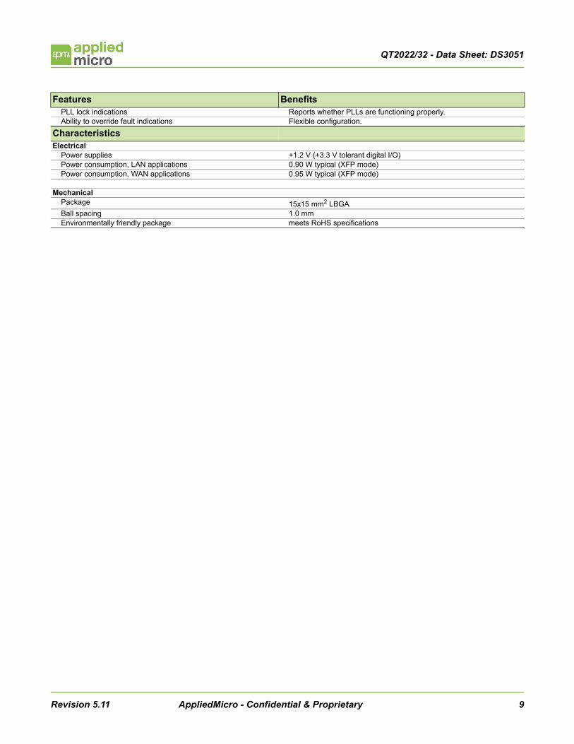
PLL lock indications Reports whether PLLs are functioning properly.Ability to override fault indications Flexible configuration.
CharacteristicsElectrical
Power supplies +1.2 V (+3.3 V tolerant digital I/O)Power consumption, LAN applications 0.90 W typical (XFP mode)Power consumption, WAN applications 0.95 W typical (XFP mode)
MechanicalPackage 15x15 mm2 LBGABall spacing 1.0 mmEnvironmentally friendly package meets RoHS specifications
Features Benefits
Revision 5.11 AppliedMicro - Confidential & Proprietary 9

QT2022/32 - Data Sheet: DS3051
3 Available Package OptionsThe body of the QT2022/32 package complies with the RoHS directive for elimination of banned materials. The sol-der balls are composed of a SnAgCu alloy, which requires a hotter thermal reflow profile for die attach. The adoption of a hotter reflow profile for the Pb-free solder presents practical difficulties in manufacturing. To ease the transition to RoHS compliant products for our customers, the product is also available with standard Sn63%/Pb37% solder balls.
The order codes for the products with leaded and lead-free solder balls are listed in Table 79 on page 219.
10 AppliedMicro - Confidential & Proprietary Revision 5.11

QT2022/32 - Data Sheet: DS3051
4 Pin Assignment and Description
4.1 QT2032 Ball Arrangement
The QT2032 comes in a 15x15 mm2 LBGA package with 1.0 mm ball pitch. The pin arrangement is shown in Table 1 and the pin assignments are described in Table 3.
Table 1: QT2032 Ball Arrangement Top View (through the package)
P N M L K J H G F E D C B A •1 TXPLL
OUTP GND SREFCLKP GND VCXOI
P GNDVCXO-CNTL
PGND EREF
CLKPPRTA
D1TxXMON
CVP
PRTAD2
PRTAD3
PRTAD4 1
2 TXPLLOUTN GND SREF
CLKN GND VCXOIN GND
VCXO-CNTL
NGND EREF
CLKNPRTA
D0TxXMON
CVN
LEGACY
TxXAUI3N
TxXAUI3P 2
3 GND GND GND GND GND GND GND TRST_N LASI LASI_
INTB TCK TXFAULT GND XV1P2 3
4 TXLEVEL
TXIPMP TXFN TXFP TV1P2
ATV1P2
A TXON MDIO MDC LED1 LED2TXOU
T_SEL
TxXAUI2N
TxXAUI2P 4
5 TV1P2 TV1P2 TV1P2 TGNDA
TGNDA
COREVDD
COREVDD
COREVDD
COREVDD
TDCC_CLK LED3
TxXAUI
_SELGND XV1P2 5
6 <noball>
TXOUTP GND GND GND GND GND GND GND TDCC TDI PHOF
F_ENTxXAU
I1NTxXAU
I1P 6
7 <noball>
TXOUTN GND GND GND GND GND GND GND TMS TDO
RxXAUI
_SELGND XV1P2 7
8 TV1P2 GND GND RGNDA GND GND GND GND GND EQ_E
Nreserv
edEEPROM_PROT
TxXAUI0N
TxXAUI0P 8
9 RV1P2 RV1P2 RV1P2 RV1P2 GND GND GND GND GND reserved
LOSOUTB
REFSEL622 GND XV1P2 9
10 <noball> RXIP reserv
edRV1P2
A GND GND GND GND GND RDCCEEPROM_S
CLXFP RxXA
UI3NRxXAUI3P 10
11 <noball> RXIN reserv
edRV1P2
ARGND
ACOREVDD
COREVDD
COREVDD
COREVDD
RDCC_CLK
EEPROM_S
DA
RESETN GND XV1P2 11
12 reserved GND reserv
edPHASE_OFF
SET
reserved
reserved
reserved
VCXOSEL62
2
VCXOONLY
LTIMEOK
RXLOSB_I
TXENAB
LE
RxXAUI2N
RxXAUI2P 12
13 RXFN ITH_LOS
RXICXP
reserved
reserved
reserved
VCXOB
RXPLLOUTP XBIAS reserv
edRxXAUI0N
RXIN_SEL GND XV1P2 13
14 RXFP RXIPMP
RXICXN
reserved
<noball>
<noball>
reserved
RXPLLOUTN
RxXLEVEL
LANMODE
RxXAUIOP GND RxXA
UI1NRxXAUI1P 14
P N M L K J H G F E D C B A
Revision 5.11 AppliedMicro - Confidential & Proprietary 11

QT2022/32 - Data Sheet: DS3051
4.2 QT2022 Ball Arrangement
The QT2022 comes in a 15x15 mm2 LBGA package with 1.0 mm ball pitch. The pin arrangement is shown in Table 2 and the pin assignments are described in Table 3. The pin assignment is shared with QT2032 except for 14 balls which are unused in the QT2022. No ball locations are moved.
Table 2: QT2022 Ball Arrangement Top View (through the package)
P N M L K J H G F E D C B A •1 TXPLL
OUTP GND unused GND unuse
d GND unused GND EREF
CLKPPRTA
D1TxXMON
CVP
PRTAD2
PRTAD3
PRTAD4 1
2 TXPLLOUTN GND unuse
d GND unused GND unuse
d GND EREFCLKN
PRTAD0
TxXMON
CVN
LEGACY
TxXAUI3N
TxXAUI3P 2
3 GND GND GND GND GND GND GND TRST_N LASI LASI_
INTB TCK TXFAULT GND XV1P2 3
4 TXLEVEL
TXIPMP TXFN TXFP TV1P2
ATV1P2
A TXON MDIO MDC LED1 LED2TXOU
T_SEL
TxXAUI2N
TxXAUI2P 4
5 TV1P2 TV1P2 TV1P2 TGNDA
TGNDA
COREVDD
COREVDD
COREVDD
COREVDD
unused LED3
TxXAUI
_SELGND XV1P2 5
6 <noball>
TXOUTP GND GND GND GND GND GND GND unuse
d TDI PHOFF_EN
TxXAUI1N
TxXAUI1P 6
7<noball>
TXOUTN GND GND GND GND GND GND GND TMS TDO
RxXAUI
_SELGND XV1P2 7
8 TV1P2 GND GND RGNDA GND GND GND GND GND EQ_E
Nreserv
edEEPROM_PROT
TxXAUI0N
TxXAUI0P 8
9 RV1P2 RV1P2 RV1P2 RV1P2 GND GND GND GND GND reserved
LOSOUTB
REFSEL622 GND XV1P2 9
10 <noball> RXIP reserv
edRV1P2
A GND GND GND GND GND unused
EEPROM_S
CLXFP RxXA
UI3NRxXAUI3P 10
11 <noball> RXIN reserv
edRV1P2
ARGND
ACOREVDD
COREVDD
COREVDD
COREVDD
unused
EEPROM_S
DA
RESETN GND XV1P2 11
12 reserved GND reserv
edPHASE_OFF
SET
reserved
reserved
reserved
unused
unused
LTIMEOK
RXLOSB_I
TXENAB
LE
RxXAUI2N
RxXAUI2P 12
13 RXFN ITH_LOS
RXICXP
reserved
reserved
reserved
unused
RXPLLOUTP XBIAS reserv
edRxXAUI0N
RXIN_SEL GND XV1P2 13
14 RXFP RXIPMP
RXICXN
reserved
<noball>
<noball>
reserved
RXPLLOUTN
RxXLEVEL
unused
RxXAUIOP GND RxXA
UI1NRxXAUI1P 14
P N M L K J H G F E D C B A
12 AppliedMicro - Confidential & Proprietary Revision 5.11

QT2022/32 - Data Sheet: DS3051
Table 3: QT2022/32 Ball Assignment & Signal Description
Ball Signal Name Dir. Type Description
CML Outputs
N6N7
TXOUTPTXOUTN
O CML 9.95 - 10.5 Gb/s transmit differential voltage outputs.100 Ω differential impedance.
D14D13
RxXAUI0PRxXAUI0N
O CML 3.125 Gb/s differential output data from QT2022/32 to XAUI interface - lane 0
A14B14
RxXAUI1PRxXAUI1N
O CML 3.125 Gb/s differential output data from QT2022/32 to XAUI interface - lane 1
A12B12
RxXAUI2PRxXAUI2N
O CML 3.125 Gb/s differential output data from QT2022/32 to XAUI interface - lane 2
A10B10
RxXAUI3PRxXAUI3N
O CML 3.125 Gb/s differential output data from QT2022/32 to XAUI interface - lane 3
G13G14
RXPLLOUTPRXPLLOUTN
O CML Clock output from receive input data PLL Used for monitoring only. Leave unconnected.
P1P2
TXPLLOUTPTXPLLOUTN(REFCLK2P,REFCLK2N)
O/I CML Configurable as either a differential transmit clock driver (default) or as a reference clock input instead of EREFCLK (with MDIO bit 1.C001h.7=1).
The output clock frequency is controlled by MDIObit 1.C001h.2. The default frequencies are:With XFP=1: divide-by-64, can be used as reference clock to the XFP module; 161.13 MHz (10GE) or 164.355 MHz (10GFC) With XFP=0: divide-by-66; 156.25MHz (10GE) or 159.375 (10GFC)
Enabling the driver circuitry is controlled by MDIO bit 1.C001h.3. By default:With XFP=1, the driver is enabledWith XFP=0, the driver is disabled
Note: for the case where the pin is configured as a reference clock input, the driver circuitry is disabled.
H1H2
VCXOCTLPVCXOCTLN
O CML QT2032:Output of phase-frequency detector which drives the external loop filter as part of the VCXO control.
QT2022:Unused. Leave unconnected.
CML Inputs
F1F2
EREFCLKPEREFCLKN
I CML LAN reference clock input for fiber-side TXPLL.156.25 MHz (10GE) or 159.375 (10GFC)On chip 50Ω terminations to 1.2 V. Requires external AC coupling.
M1M2
SREFCLKPSREFCLKN
I CML QT2032:SONET reference clock input for fiber-side TXPLL in WAN-mode155.52 MHz or 622.08 MHz selected by REFSEL622 pin;AC coupled with on chip 50Ω terminations to 1.2 V
QT2022:Unused. Leave unconnected.
Revision 5.11 AppliedMicro - Confidential & Proprietary 13

QT2022/32 - Data Sheet: DS3051
K1K2
VCXOIPVCXOIN
I CML QT2032:Input clock from VCXO when an external VCXO is used for the fiber side TXPLL reference clock input in WAN-mode; 155.52 MHz or 622.08 MHz selected by VCXOSEL622 pin;AC coupled with on chip 50Ω terminations to 1.2 V.
QT2022:Unused. Leave unconnected.
N10N11
RXIPRXIN
I CML 10 Gb/s receive data in, 100 Ω differential impedance.
A8B8
TxXAUI0PTxXAUI0N
I CML Transmit 3.125 Gb/s data to QT2022/32 from XAUI interface - lane 0
A6B6
TxXAUI1PTxXAUI1N
I CML Transmit 3.125 Gb/s data to QT2022/32 from XAUI interface - lane 1
A4B4
TxXAUI2PTxXAUI2N
I CML Transmit 3.125 Gb/s data to QT2022/32 from XAUI interface - lane 2
A2B2
TxXAUI3PTxXAUI3N
I CML Transmit 3.125 Gb/s data to QT2022/32 from XAUI interface - lane 3
DC Monitor Points
D1 TxXMONCVP O analog Monitor test point for the transmit XAUI interface (DC signal).Used for monitoring only. Leave unconnected.
D2 TxXMONCVN O analog Monitor points for the transmit XAUI interface (DC signal)Used for monitoring only. Leave unconnected.
Connection Points for External Components
M13 RXICXP analog Connection point for external 100 nF cap to ground
M14 RXICXN analog Connection point for external 100 nF cap to ground
L12 PHASE_OFFSET analog For test purposes only.
N13 ITH_LOS analog Internal fiber receive path loss of signal (LOS) detector threshold adjust. See Section 8.7.1 on page 72 for details.
F14 RxXLEVEL analog connection point for external resistor to set receive XAUI drivers’ output level.
F13 XBIAS analog XAUI bias current control 6.49 kΩ resistor to GND.
P14P13
RXFPRXFN
analog Receive charge pump filter connection points see “External Components” on page 209 for external component connections
N14 RXIPMP analog Receive charge pump current control 6.49 kΩ resistor to GND
P4 TXLEVEL analog external resistor used to control 10.3125 Gb/s output data amplitude.
L4M4
TXFPTXFN
analog Transmit loop filter - see “External Components” on page 209 for external components
Table 3: QT2022/32 Ball Assignment & Signal Description (Continued)
Ball Signal Name Dir. Type Description
14 AppliedMicro - Confidential & Proprietary Revision 5.11

QT2022/32 - Data Sheet: DS3051
N4 TXIPMP analog Transmit charge pump current control 6.49 kΩ resistor to GND
CMOS Inputs (note all CMOS inputs are 3.3V tolerant and all CMOS inputs with pullups are to 1.2V)
E6 TDCC I CMOS QT2032:Transmit data communication channel input for both section and line SONET overhead data; clocked in using the TDCC_CLK output. Please see Section 7.3.8, “Transport Overhead Serial Interface,” on page 48.QT2022:Unused. Connect to GND.
E14 LANMODE I CMOS with 50kΩpullup
QT2032:LAN/WAN Mode select0 = WAN mode enabled 1 = LAN mode enabled (default)When LANMODE = 1, the chip will not operate in WAN mode and access to all WIS registers is disabled. When LANMODE = 0, the chip will default to WAN mode operation but can be set to operate in LAN mode by setting MDIO register bit 2.7.0 to 0.
QT2022:Unused. Leave unconnected.
C9 REFSEL622 I CMOS with 50 kΩpulldown
QT2032:SREFCLK frequency selection0 = 155.52 MHz (default) 1 = 622.08 MHz
QT2022:Unused. Leave unconnected.
G12 VCXOSEL622 I CMOS with 50kΩpulldown
QT2032:VCXO frequency selection0 = 155.52 MHz (default) 1 = 622.08 MHz
QT2022:Unused. Leave unconnected.
H13 VCXOB I CMOS with 50kΩpullup
QT2032:VCXO control loop enable pin. A low-level configures the chip to implement a PLL using an external VCXO - see description in Section 6.2.4, “VCXO PLL,” on page 32.0 = enabled 1 = disabled (default)
QT2022:Unused. Leave unconnected.
F12 VCXOONLY I CMOS with 50kΩpulldown
QT2032:Input to indicate that the VCXO is the only reference clock available (i.e. there is no SREFCLK input - so in non-linetiming mode, there is no switchover to it)0 = there is a SREFCLK input in WAN mode (default) 1 = there is no SREFCLK input in WAN mode (i.e. VCXO alone. Also set REFSEL622 = VCXOSEL622)
QT2022:Unused. Leave unconnected.
Table 3: QT2022/32 Ball Assignment & Signal Description (Continued)
Ball Signal Name Dir. Type Description
Revision 5.11 AppliedMicro - Confidential & Proprietary 15

QT2022/32 - Data Sheet: DS3051
C6 PHOFF_EN I CMOS with 50kΩpulldown
Phase Offset Enable pin (NEW).Enables adjustment of Receive CDR decision phase from nominal. Used in conjunction with the PHASE_OFFSET pin. For test purposes only.0 = phase offset control disabled (default)1 = phase offset control enabled.
C2 LEGACY I CMOS with 50kΩpulldown
0 (default) = new register map definitions1=reverts to 2021 register map definitions (see LEGACY mode description)
C13 RXIN_SEL I CMOS with 50kΩpulldown
Polarity control for RXI, 50 kΩ pulldownRXIN_SEL=0 default polarityRXIN_SEL=1 inverted polarity
C5 TxXAUI_SEL(SCAN_EN)
I CMOS with 50kΩpulldown
XAUI Transmit path lane order control, 50 kΩ pulldown0 = default lane ordering 1 = inverted lane orderingEnable scan in scan mode
C7 RxXAUI_SEL I CMOS with 50kΩ pulldown
XAUI receive path lane order control, 50 kΩ pulldown0 = default lane ordering 1 = inverted lane ordering
D12 RXLOSB_I(XFPRXLOS)
I CMOS with 50kΩ pullup to 1.2V
Receive optical signal loss indicator input (can be driven directly by LOSOUTB or by an external source)When XFP=0, active low indicates RX signal losswith XFP=1, active high indicates RX signal loss(See Section 8.2.2 on page 54)
C10 XFP I CMOS with 50kΩ pulldown
XFP application mode select;0 = non-XFP application, default; high-sensitivity input selected on 10Gb/s input1 = XFP application; equalization option selected on 10Gb/s input (can be over-ridden via MDIO register bit 1.C030h.6 - ‘override_xfp_eqn’). Also changes function of TXPLLOUT, LOSOUTB, TXFAULT, TXON, TXENABLE, EEPROM_PROT, RXLOSB_I and TRST_N.
E8 EQ_EN I CMOS with 50kΩ pulldown
Receive Equalizer Enable pin (NEW). Allows receive equalizer to be enabled.0 = equalizer state determined by XFP pin (default)1 = equalizer on.
C8 EEPROM_PROT(XFPMODABS)
I CMOS with 50kΩ pullup to 1.2V
With XFP=0, EEPROM interface write protection pin; Scan enable when in scan mode 1 (default) = no writes to protected EEPROM registers allowed; With XFP=1, high level indicates XFP module absent
F4 MDC I CMOS MDIO interface clock
C4 TXOUT_SEL I CMOS with 50kΩ pulldown
TXOUT polarity control, 50 kΩ pulldown0 = default polarity1 = inverted polarity
E3 LASI_INTB(XFPINTB)
I CMOS with 50kΩ pullup to 1.2V
With XFP=0, Active low interrupt input to LASI; (See Section 8.2.12 on page 57).With XFP=1, active low interrupt input indicating XFP module fault condition.
Table 3: QT2022/32 Ball Assignment & Signal Description (Continued)
Ball Signal Name Dir. Type Description
16 AppliedMicro - Confidential & Proprietary Revision 5.11

QT2022/32 - Data Sheet: DS3051
C3 TXFAULT(XFPMODNR)
I CMOS with 50kΩ pullup to 1.2V
With XFP=0, External laser or laser-driver fault indicator as per XENPAK MSAlogic low = normal operationlogic high = fault condition(See “Laser Driver Enable Pin (TXENABLE)” on page 69.)With XFP=1, high level indicates XFP module not ready
E2E1C1B1A1
PRTAD<0>PRTAD<1>PRTAD<2>PRTAD<3>PRTAD<4>
I CMOSno pullup or pulldown
Port address for MDIO transactions. See “Management Frame Format” on page 74. for more information on the MDIO/C interface.
C11 RESETN I CMOS with hysteresis25kΩ pullup
reset, active lowlogic low = reset conditionlogic high = normal operationNote: the TAP port controller is only reset by the TRST_N pin and is unaffected by RESETNNote: in a module application XFP=0 & the external cap for the powerup reset must be connected to the TRST_N input. For further details, please see Section 18.5 on page 210
D6D3G3
E7
TDITCKTRST_N
TMS
III
I
CMOS
36kΩ pullup(no pullup/dn)25kΩ pullup
36kΩ pullup
Test pins for Test Access Port (or internal scan testing when SCAN instruction written to TAP). Test data input (scan in) Test clock input (scan clock) Test reset, active low (hold high for scan)
with XFP=0, also resets the core and is to be used as the connection point for an external cap to GND for a powerup reset.
Test mode select, active low (hold high for scan)
CMOS Outputs (note: all CMOS outputs are 3.3V tolerant open drain)
E12 LTIMEOK O CMOS open drain(see note1)
QT2032:Line-timing internal enable indication.logic high = conditions are valid for line-timing operation and it is internally enabled.A low level can be used to center the external VXCO in a VXCO-only application.(see Section 6.2.4, “VCXO PLL,” on page 32 for a description of the logic)
QT2022:Unused. Connect to GND.
E10 RDCC O CMOS open drain(see note1)
QT2032:Receive data communication channel output for both section and line SONET overhead data; timed from the RDCC_CLK clock output. Please see Section 7.3.8, “Transport Overhead Serial Interface,” on page 48.
QT2022:Unused. Connect to GND.
E11 RDCC_CLK O CMOS open drain(see note1)
QT2032:Gapped clock used for timing RDCC output. Please see Section 7.3.8, “Transport Overhead Serial Interface,” on page 48.
QT2022:Unused. Connect to GND.
Table 3: QT2022/32 Ball Assignment & Signal Description (Continued)
Ball Signal Name Dir. Type Description
Revision 5.11 AppliedMicro - Confidential & Proprietary 17

QT2022/32 - Data Sheet: DS3051
E5 TDCC_CLK O CMOS open drain(see note1)
QT2032:Gapped clock used for timing TDCC input.Please see Section 7.3.8, “Transport Overhead Serial Interface,” on page 48
QT2022:Unused. Connect to GND.
D7 TDO O CMOS open drain(see note1)
Test data output (scan out when SCAN instruction written to TAP).)
F3 LASI O CMOS open drain Link Alarm Status Interrupt (LASI)logic low = Interrupt assertedlogic high =No alarm interrupt assertedSee “Link Alarm Status Interrupt Pin (LASI)” on page 62.
C12 TXENABLE(XFPTXDIS)
O CMOS open drain With XFP=0, Active high laser driver enable as per XENPAK MSA(see “Laser Driver Enable Pin (TXENABLE)” on page 69)With XFP=1, drives TX_DIS input of XFP module
D9 LOSOUTB(XFPPDN)
O CMOS (see note1) open drain
With XFP=0, low level indicates when the input signal applied at RXIP/N is below a threshold which can be adjusted via the resistor connected to the ITH_LOS pinWith XFP=1, drives P_DOWN/RST input of XFP module
Bidirectional CMOS IO (note: all CMOS I/O are 3.3V tolerant & outputs are open drain)
D10 EEPROM_SCL I/O CMOS (see note1) bidirectional open drainhysteresis
EEPROM serial interface clock. can be tristated via MDIO register 1.C024h.0 This is a bidirectional pin to allow an external device to take control of the EEPROM I2C interface.With XFP=1, drives the XFP module I2C interface.
D11 EEPROM_SDA I/O CMOS (see note1) bidirectional open drainhysteresis
EEPROM interface serial address/data. With XFP=1, drives the XFP module I2C interface.
G4 MDIO I/O CMOSbidirectional open drain
MDIO Interface serial data signalExternal pullup to 1.2V required. Please see Section 9.5 on page 74 for details.
H4 TXON(XFPMODDESEL)
I/O CMOS bidirectional open drain with 50kΩ pullup to 1.2V(output in XFP mode)
With XFP=0, low power mode control input0 = low power mode (only the MDIO, EEPROM and DOM functions are active with an external reference clock applied at EREFCLKP/N)1 = normal operating mode, defaultWith XFP=1, output to drive the MOD_DESEL input of an XFP module
Miscellaneous
E4 LED1 I/O CMOS input or 10mA open drain output
LED driver and General Purpose I/O:Can be configured as a LED driver output or as a GPIO via MDIO register bits 1.D006h.2:0. The default configuration is as a LED driver.As an input, its state is displayed in MDIO register bit 1.D006h.5; as an output it can be driven by MDIO register bits 1.D006h.2:0 or other internal status signals (see Section 8.6 on page 70)
Table 3: QT2022/32 Ball Assignment & Signal Description (Continued)
Ball Signal Name Dir. Type Description
18 AppliedMicro - Confidential & Proprietary Revision 5.11

QT2022/32 - Data Sheet: DS3051
Note1: All CMOS pins are compatible with 3.3V logic. All CMOS inputs with internal pullups are to 1.2V. All CMOS outputs are open drain.
D4 LED2 I/O CMOS input with 50kΩ pullup to 1.2V, or 10mA open drain output
LED driver and General Purpose I/O:Can be configured as a LED driver output or as a GPIO via MDIO register bits 1.D007h.2:0. The default configuration is as a LED driver.As an input, its state is displayed in MDIO register bit 1.D006h.5; as an output it can be driven by MDIO register bits 1.D007h.2:0 or other internal status signals (see Section 8.6 on page 70)If this pin is held low during a hard reset, it will enable ‘two-byte’ addressing of an peripheral I2C device. Please see Section 10.6 on page 89 for details.
D5 LED3 I/O CMOS input or 10mA open drain output
LED driver and General Purpose I/O:Can be configured as a LED driver output or as a GPIO via MDIO bits 1.D008h.2:0. The default configuration is as a LED driver.As an input, its state is displayed in MDIO register bit 1.D008h.5, as an output it can be driven by MDIO bits 1.D008h.2:0 or other internal status signals (see Section 8.6 on page 70)
Reserved pins
D8E9M10M11H12J12K12M12P12E13J13K13L13H14L14
Reserved. Leave unconnected.
Table 3: QT2022/32 Ball Assignment & Signal Description (Continued)
Ball Signal Name Dir. Type Description
Revision 5.11 AppliedMicro - Confidential & Proprietary 19

QT2022/32 - Data Sheet: DS3051
Table 4: Supply Pad and Ball Assignment and Description
Supply (#) Descriptionballs
15x15 mm2 package
TV1P2 (4) 1.2V Supply for transmit fiber side circuits M5,N5,P5,P8
GND (54) Ground G1,J1,L1,N1,G2,J2,L2,N2,B3,H3,J3K3,L3,M3,N3,P3,B5,F6,G6,H6,J6,K6L6,M6,B7,F7,G7,H7,J7,K7,L7,M7,F8G8,H8,J8,K8,M8,N8,B9,F9,G9,H9,J9K9,F10,G10,H10,J10,K10,B11,N12B13,C14
TV1P2A (2) 1.2V Supply for transmit PLL K4,J4
RV1P2 (4) 1.2V Supply for fiber receive side circuits L9,M9,N9,P9
RV1P2A (2) 1.2V Supply for receive PLL L10,L11
XV1P2 (6) 1.2V supply for XAUI side A3,A5,A7,A9,A11,A13
COREVDD (8) 1.2V Supply for CMOS digital logic F5,G5,H5,J5,F11,G11,H11,J11
RGNDA (2) Receive Analog Ground K11,L8
TGNDA (2) Transmit Analog Ground K5,L5
20 AppliedMicro - Confidential & Proprietary Revision 5.11

QT2022/32 - Data Sheet: DS3051
5 Datapath DescriptionThis section describes the functional blocks of the QT2022/32. These are illustrated in Figure 2.
Figure 2: QT2022/32 Functional Block Diagram
5.1 Transmit Path
5.1.1 XAUI CDR and DemultiplexerAt the transmitter XAUI interface, clock and data are recovered for each of the four 3.125Gb/s input lanes. The dif-ferential receivers used at this interface have 100 Ω differential input impedance and are intended to be AC coupled or 1.2 V CML DC coupled. The data on each channel is then demultiplexed/deserialized before being passed to the next block. A clock is recovered for each lane. Each lane outputs a status bit, xtxlock<3:0>, which is high when the CDR circuit is in lock. A phase-adjust FIFO aligns the four lanes using the Lane 1 recovered clock.
5.1.2 XAUI Code SynchronizationThe XAUI interface demultiplexer has no prior knowledge of code word boundaries and must determine where each 8B/10B character starts and ends. To achieve this, the code synchronization block searches the data stream for the unique comma character, /K/, in order to determine the 10 bit code word boundaries for each lane. The delimited code words are passed to the Frame Deskew block. The code synchronization status is displayed in Reg-ister bits 4.18h.3:0. The comma characters, /K/, are found in the XAUI data stream in the IPG between packets.
TXOUT
TxXAUI0CDR
Driver
RXIN
Output10b/8bDecoder GearboxAlign
TxXAUI1
TxXAUI2
3.125 Gb/s
TxXAUI3
Scrambler
RxXAUI0DRV
66b/64bDecoder
RateAdjust
FrameRxXAUI1
RxXAUI2
RxXAUI3
Sync
limiting
PMA systemloopback
PMA networkloopback
PCS loopback
AMCC XGXSloopback
XGXSloopbacknetwork system
AMCC
WIS
WIS
WISloopback
TX
8b/10bEncoder
CDR
CDR
CDR
DRV
DRV
DRV
De-scrambler
64b/66bEncoderRate
AdjustPhase
Adjust &Demux
CDRRX
Code
MDIO ControlInterface
MDIO
MDCEEPROM / DOM
Interface
EEPROM_SDAEEPROM_SCL
EEPROM_PROT
Sync
CodeSync
CodeSync
CodeSync
amp
RXPLLOUT freqmon
sync_err
LOSdetector
LOSOUTB
Demux
TXPLLOUTclockgenerator
EREFCLKSREFCLK
VXCOI
Mux(QT2032
only)
(QT2032only)
(QT2032 only)
(QT2032 only)
Revision 5.11 AppliedMicro - Confidential & Proprietary 21

QT2022/32 - Data Sheet: DS3051
If any single lane loses signal (no transitions detected), the code synchronization block will not attempt to achieve alignment on the XAUI input lanes. The QT2022/32 will report ‘loss of sync’ on all 4 lanes. However, when valid data is received on all 4 lanes, the code synchronization block is fully active. If no /K/ charac-ters are detected on a given lane, the QT2022/32 will report ‘loss of sync’ independently for each lane.
5.1.3 XAUI Lane AlignThe incoming XAUI data may be skewed due to varying off-chip transmission delays between the four lanes. The deskew operation is done by aligning the /A/ code characters on all four lanes. The /A/ codes appear randomly in the idle data stream and are transmitted simultaneously at the source on all four channels as a single column of data, ||A||. The alignment is done by placing the data from each channel in a FIFO and adjusting the read pointer of each FIFO so that the /A/ codes are read out simultaneously when they occur.The QT2022/32 can tolerate a skew of up to 5 code words, or 50 bits between any two lanes at the TxXAUI input pins. (The IEEE 802.3 requirement is for a maximum of 40 bit skew between lanes.)
5.1.4 8B/10B DecodingEach 10 bit code word is decoded into 8 data bits and 1 control bit. The 8 data bits and 1 control bit are then passed on to the rate adjust function. Any 8B/10B coding errors are counted on a per lane basis. For each lane, errors are reported in an 8 bit, non-roll-over counter that is cleared on read. The four counters for Lane 0 to Lane 3 are located in the lower byte of MDIO registers 4.C030h - 4.C033h respectively.
5.1.5 Transmit Rate AdjustData is written into a rate compensation FIFO. The outgoing data is read out using a clock derived from the exter-nal reference clock. Since these clocks are derived from different sources, a rate adjust operation needs to be performed. The rate compensation block accomplishes this by either adding or dropping idle codes or sequence ordered sets from the data stream. The minimum inter packet gap (IPG) of five characters and sequence ordered set messages are always maintained.Proper rate compensation will always be performed when the clock rates are within 200ppm (total). The QT2022/QT2032 can tolerate up to 2 back-to-back 9600 byte jumbo frames with minimum IPG. If the clock rate difference exceeds 200ppm or multiple back-to-back jumbo frames are transmitted, one or more packets may be corrupted. Transmit rate adjust operation is monitored in MDIO register 4.C002h. This register flags idle code removal and insertion in bits 15:14 (normal operation), as well as overflow/underflow in bits 9:8 (fault condition).
5.1.6 64B/66B EncodingThe encoder takes 64 bits of input data and the associated 8 bit control word and creates a new 66 bit data bus. The 66 bits are composed of 2 sync bits followed by 64 bits of data. The sync bits are used to synchronize the data stream on a frame boundary. The sync bits <1:0> are 10 if 64 bit data bus is composed solely of data words. If the bus contains 1 or more control words, the sync bits <1:0> are set to 01 and are followed by a 8 bit type data. The type word indicates the content of the following 56 bits of data. The sync bit values of 00 or 11 are invalid for the sync bits.Incoming control words are converted from 8 bits to 7 bits. Data words are not altered. When combinations of data and control words are used in a bus, extra bits are inserted if needed at the boundary between the data and control words to make the total number of bits 64. Ordered set control codes are encoded using a combination of the block’s type field and a 4 bit O code for each ordered set.
5.1.7 Scrambler
The scrambler polynomial is 1+x39+x58. Only the 64 data bits pass through the scrambler. The sync bits are not scrambled. The scrambler can be bypassed by setting the MDIO register bit 3.C000h.2.
22 AppliedMicro - Confidential & Proprietary Revision 5.11

QT2022/32 - Data Sheet: DS3051
Figure 3: Transmit Scrambler
5.1.8 Gear BoxThe gear box converts the data from a 66 bit wide data bus at 156.25 Mb/s to a 64 bit wide bus at 161.1328 Mb/s. This step is required to prepare the data for serialization in the next functional block.
5.1.9 Transmit WAN Interface Sublayer (WIS) (QT2032 Only)The TX WIS block accepts data from the gear box and maps it into the payload of the transmitted STS-192C WIS frame stream. Fixed stuff octets are added, together with a set of Path Overhead octets, to create a Synchronous Payload Envelope (SPE). Line and Section Overhead octets are combined with the SPE and then scrambled using the frame-synchronous scrambler to produce the final transmitted WIS frame. The WIS continuously generates one WIS frame every 125 μs.
5.1.10 Transmit Multiplexer and Clock GenerationA clock divider generates the clock frequencies required to multiplex the 64 bit wide bus coming from the TX WIS into a single 10 Gb/s output, from the locally generated 10 GHz clock.
5.1.11 Output Data DriverThe output driver has a nominal output voltage of 250 mVpp per side. TXOUTN and TXOUTP are both terminated on chip with 50 Ω to 1.2V. The output level can be adjusted via an external resistor connected to TXLEVEL. The output polarity can be inverted by pulling pin TXOUT_SEL high.
5.1.12 Line Timing ModeLine timing is used in the QT2032 to ensure the transmitted data is synchronized to the SONET network. In line timing mode, the reference clock used for the transmit PLL is derived from the recovered receive clock. Line timing mode is enabled by the Line Timing Control Register. Please see Section 6, “Datapath Clocking,” on page 26 for details. Line timing is not supported in the QT2022.
S0 S1 S2 S38 S40 S56 S57
Serial Data Input
Scrambled Data Output
Revision 5.11 AppliedMicro - Confidential & Proprietary 23

QT2022/32 - Data Sheet: DS3051
5.2 Receive Path
5.2.1 Limiting Amp The receiver input contains a limiting amplifier designed for a differential CML voltage across the RXIN inputs. The input polarity can be selected by pin RXIN_SEL. The input sensitivity is good enough to eliminate the need for an external limiting amp in many applications. For a system card application, the XFP input pin is set high and an input equalization circuit is activated to allow for longer FR4 traces. It can be deactivated by asserting MDIO register bit 1.C030h.6.AC coupling of the 10 Gb/s input signal(s) is required to achieve good sensitivity as it reduces the amount of 1/f noise at the input to the QT2022/32.
5.2.2 Loss of Signal DetectorThe RX input limiting amplifier also incorporates a loss of signal detector. The loss of signal detector is disabled if the input equalization circuit is activated (see Section 5.2.1 above). The LOSOUTB signal is available as an output. The loss of signal threshold (in mVpp) is controlled by adjusting the value of the external resistor connected to the ITH_LOS pin. The threshold includes built-in hysteresis to prevent LOSOUTB chatter. The LOSOUTB signal can be externally connected to the RXLOSB_I input (this allows for the option of using an external TIALA with its own loss of signal detector).
5.2.3 Clock RecoveryThe output of the limiting amp goes to a clock and data recovery (CDR) circuit. When the PLL is frequency locked to the incoming data, the internal signal, frxlock is asserted. When frxlock is low the receive data outputs RxX-AUI<0:3> will transmit idle frames and error codes. The state of frxlock is reflected in the ‘PMA receive link status’ bit, 1.1.2, a latched low register bit whose value is determined by the equation {frxlock AND RXLOSB_I}. The state of the RXLOSB_I input is shown separately in Register bit 1.10.0.The PLL uses an external loop filter. See Section 18.1, “External Components,” on page 209 for the loop filter com-ponents and values.
Recovered Clock Frequency Monitoring and RXCLK
When the receive recovered clock is more than 500 ppm from the transmit reference clock, a synchronization error is declared and the internal signal sync_err goes high. sync_err can be viewed at MDIO register 1.C001h.1. This is a latched high register bit that is cleared on read. On powerup or reset, the register must be read to clear it.
5.2.4 Demultiplexer and Clock DividerAll clocks needed for the demultiplexer and the reset of the receive path are generated in this block by dividing down the 10 GHz recovered clock. The demultiplexer converts the 10 Gb/s serial incoming data into 64 parallel bits. A divide-by-64 recovered clock can be output at RXPLLOUT by setting MDIO register bit 1.C001h.6 = 1.
5.2.5 Receive WAN Interface Sublayer (WIS) (QT2032 Only)The RX WIS block receives data from a SONET link and extracts the Ethernet payload from the STS-192c SPE. It also monitors the integrity of data at the Section, Line and Path levels and monitors both near and far end faults. The WIS receive and transmit blocks can be bypassed by setting MDIO register 2.7.0 to 0 or if LANMODE = 1.
24 AppliedMicro - Confidential & Proprietary Revision 5.11

QT2022/32 - Data Sheet: DS3051
5.2.6 Frame SynchronizationThe frame synchronizer takes the 64 bit wide data bus output from the demultiplexer and converts it to a 66 bit wide data bus. The 66 bits are composed of 2 sync bits followed by 64 bits of data. The sync bits are used to synchro-nize the data stream on a frame boundary. The bus rate at each stage will depend on the selected protocol. The chip also monitors invalid sync header bits. Valid sync bits include ‘01’ and ‘10’. The combinations ‘11’ and ‘00’ are invalid. When an invalid sync header is detected, a 6-bit counter is incremented. This counter is located in MDIO register bits 3.33.13:8. This is a read only, non-rollover counter that is cleared when read. The counter will count a maximum of 16 sync header errors in a 125 μs window. When there are 16 or more sync header errors in a 125μs window, the ‘hi_ber’ flag is set to 1 in MDIO register bit 3.32.1 (3.20h.1). This is a read only register bit that is cleared when read. The algorithm for counting sync header errors and detecting ‘hi_ber’ follows the ‘BER monitor state machine’ described in IEEE 802.3 Figure 49-13.
5.2.7 DescramblerThe descrambler processes the payload to reverse the effect of the scrambler on the payload. The descrambler is self-synchronizing. It calculates the inverse of the scrambler function using the polynomial 1+x39+x58. Only the 64 data bits are passed through the descrambler. The descrambler is bypassed when the scrambler bypass mode is enabled through MDIO register 3.C000h.1.
Figure 4: Receive Descrambler
5.2.8 66B/64B DecoderThe decoder performs the inverse function of the encoder. This block converts the 64 bit payload back into the orig-inal eight 8-bit codes. Valid code word formats are described in IEEE 802.3-2005 Figure 49-7.
5.2.9 Receive Rate AdjustData from the 66B/64B decoder is written into a rate compensation FIFO using the fiber recovered clock. The out-going data is read out using the XAUI reference clock. Due to the fact that these clocks are derived from different sources, a rate adjust operation needs to be performed. The rate compensation block accomplishes this by either adding or dropping Idle ordered_sets, as required, from the data stream. The minimum inter packet gap of five characters and sequence ordered set messages are maintained.Receive rate adjust operation is monitored in MDIO register 4.C002h. This register flags idle code removal and insertion in bits 13:12 (normal operation), as well as overflow/underflow in bits 7:6 (fault condition).
S0 S1 S2 S38 S39 S56 S57
Scrambled Data Input
Serial Data Output
Revision 5.11 AppliedMicro - Confidential & Proprietary 25

QT2022/32 - Data Sheet: DS3051
5.2.10 8B/10B EncoderThe data bus is divided into four 8-bit wide data channels. Each of the four channels has independent 8B/10B encoders which will convert the 8 bit data lanes into 10 bit code words. Either a positive or negative disparity 10 bit code word will be selected, depending on the running disparity.
5.2.11 Receive Multiplexer and XAUI InterfaceAfter 8b/10b encoding has been added, the receive multiplexer serializes data words to form four 3.125Gb/s output data lanes.The XAUI output drivers provide low-swing differential outputs with 100 Ω differential output impedance and are intended to be AC coupled. The 3.125 GHz timing is derived from the reference clock, EREFCLK.
6 Datapath ClockingThis section explains the clocking architecture and features of the QT2022 & QT2032.
6.1 LAN Application Timing Modes (QT2022 and QT2032)
6.1.1 Timing Architecture in LAN ModeThis section describes the timing of the QT2022. The QT2032 will follow this timing architecture when placed in LAN mode. In LAN mode, the RxXAUI and TX Fiber quadrants share timing references, but are generally independent of the TxXAUI and RX Fiber quadrants. The timing architecture and timing paths in LAN mode are illustrated in Figure 5.
Figure 5: LAN Mode Timing (QT2022 and QT2032)
RX Data Path
TX Data Path
CDR
CDR
CDR
CDR
RX PLL
RX CDR
TX PLL
156.25 MHzXO
AlternateXO
TxXAUI0P/N
TxXAUI1P/N
TxXAUI2P/N
TxXAUI3P/N
RxXAUI2P/N
RxXAUI1P/N
RxXAUI2P/N
RxXAUI3P/N
TXOUTP/N
RXIP/N
EREFCLK SREFCLK
Coarse control voltage used to center CDR VCO tuning range.
RX XAUI Processing
TX Fiber Processing
TX XAUI Processing
Rate Compensation
RX Fiber Processing
Rate Compensation
Timing Path
Coarse Control Voltage
Reference used to center CDR VCO when TX Fiber Input signal is failed.
TXPLLOUT
RX Fiber Recovered Clock may be used as timing reference. Test mode only.
Fiber Interface
TX XAUI Inputs
TX Fiber Output
TX Fiber Input
XAUI Interface
RX XAUI Outputs
26 AppliedMicro - Confidential & Proprietary Revision 5.11

QT2022/32 - Data Sheet: DS3051
The TX Fiber Output derives timing from a 156.25 MHz reference applied at EREFCLK or an alternate reference applied at TXPLLOUT. When applying an alternate reference to TXPLLOUT, the TXPLLOUT output driver must be disabled using MDIO bit 1.C001h.3. Selection of the desired reference is determined by the state of MDIO bit 1.C001h.7. Refer to Table 7 on page 35 for details. The TX PLL generates a 10 GHz clock from the reference by multiplying the frequency. The TX PLL output provides a clock for the TX Fiber Processing Block and Outputs.The RX Fiber CDR locks to the received signal and generates a recovered clock. The recovered clock provides timing to the RX Fiber Processing Block. When a SYNCERR is generated, the RX Fiber Input CDR will lock to the reference applied to the selected reference, either EREFCLK or TXPLLOUT, to pull the frequency back to nominal. Once the SYNCERR has cleared, the CDR will attempt to lock to the RX Fiber Input signal.The RxXAUI Outputs derive timing from the TX PLL. The RX PLL generates the 3.125 GHz clock from a reference from the TX PLL. The RX PLL output provides a clock for the RX XAUI Processing Block and Outputs.For each TxXAUI Input, a CDR locks to the received signal and generates a recovered clock. The recovered clock from lane 1 (TxXAUI1) provides a clock for the TxXAUI Processing Block. Transfer of data across clock boundaries along each data path is accomplished through rate compensation blocks.
6.1.2 Forced Line Timing ModeThe Forced Line Timing mode forces the TX Fiber Output to derive timing from the RX Fiber Input recovered clock. The Forced Line Timing mode is useful for various test scenarios or implementations where the timing is controlled externally. Forced Line Timing is controlled by MDIO register bit 1.C001h.9.
6.2 WAN Application Timing Modes (QT2032 Only)This section describes additional timing modes supported only by the QT2032. The timing paths through the QT2032 vary depending upon the mode of the device. Some modes that affect these paths include:
1. Fiber Interface Mode: either LAN or WAN, see Section 8.3.1 on page 59.2. VCXO PLL Mode: enabled or disabled, see Section 6.2.4 on page 32.3. Line Timing Mode: Disabled, Automatic, or Forced, see Section 6.2.2 on page 30.
In order to understand the relationship between timing reference and the behavior of input and output signals it is important to understand the general timing architecture of the QT2032. In the following sections, the timing archi-tecture in the WAN mode is explained.
6.2.1 Timing Architecture in WAN mode (QT2032 Only)In WAN mode, each quadrant TxXAUI, RxXAUI, RX Fiber, and TX Fiber is independently timed. The typical timing architecture and timing paths in WAN mode are illustrated in Figure 5. An optional configuration in VCXOONLY mode (VCXOB = 0 and VCXOONLY = 1) where the VCXO can provide a reference frequency is also illustrated in Figure 7.
Revision 5.11 AppliedMicro - Confidential & Proprietary 27

QT2022/32 - Data Sheet: DS3051
Figure 6: WAN Mode Timing with Fixed Frequency Reference
VCXO PLL includes external VCXO, op amp, and filter components.
RX Fiber Recovered Clock used for line timing.
Reference used to center CDR VCO when input signal is failed.
RX Data Path
TX Data Path
CDR
CDR
CDR
CDR
RX PLL
RX CDR
TX PLL
156.25 MHzXO
155.52 MHzor
622.08 MHzXO
Fiber Interface
TxXAUI0P/N
TxXAUI1P/N
TxXAUI2P/N
TxXAUI3P/N
RxXAUI2P/N
RxXAUI1P/N
RxXAUI2P/N
RxXAUI3P/N
TX XAUI Inputs
TXOUTP/N
RXIP/N
EREFCLK SREFCLK
VCXO PLL
TX Fiber Output
TX Fiber Input
RX XAUI Processing
TX Fiber Processing
TX XAUI Processing
Rate Compensation
RX Fiber Processing
Rate Compensation
Timing Path
XAUI Interface
RX XAUI Outputs
Coarse Control Voltage
TXPLLOUT
Coarse control voltage used to center CDR VCO tuning range.
VCXO PLL includes external VCXO, op amp, and filter components.
RX Fiber Recovered Clock used for line timing.
Reference used to center CDR VCO when input signal is failed.
RX Data Path
TX Data Path
CDR
CDR
CDR
CDR
RX PLL
RX CDR
TX PLL
156.25 MHzXO
155.52 MHzor
622.08 MHzXO
Fiber Interface
TxXAUI0P/N
TxXAUI1P/N
TxXAUI2P/N
TxXAUI3P/N
RxXAUI2P/N
RxXAUI1P/N
RxXAUI2P/N
RxXAUI3P/N
TX XAUI Inputs
TXOUTP/N
RXIP/N
EREFCLK SREFCLK
VCXO PLL
TX Fiber Output
TX Fiber Input
RX XAUI Processing
TX Fiber Processing
TX XAUI Processing
Rate Compensation
RX Fiber Processing
Rate Compensation
Timing Path
XAUI Interface
RX XAUI Outputs
Coarse Control Voltage
TXPLLOUTTXPLLOUT
Coarse control voltage used to center CDR VCO tuning range.
28 AppliedMicro - Confidential & Proprietary Revision 5.11

QT2022/32 - Data Sheet: DS3051
Figure 7: WAN Mode Timing without Fixed Frequency Reference
The TX Fiber Output derives timing either from a 155.52 MHz or 622.08 MHz reference applied at SREFCLK (or VCXOI when in VCXOONLY mode) or the received signal on the RX Fiber Input. The TX PLL generates a 10 GHz clock from the selected reference by multiplying the frequency. The TX PLL output provides timing for the TX Fiber Processing Block and Output. By default the TX PLL will lock to the reference applied at SREFCLK (or VCXOI when in VCXOONLY mode), however it may optionally lock to the recovered clock from the RX Fiber CDR as explained in Section 6.2.2 on page 30. In order to reduce phase noise from the selected reference and conse-quently on the TX Fiber Output, an optional VCXO PLL may be used to filter phase noise on the selected reference, as explained in Section on page 32.The RX Fiber CDR locks to the received signal and generates a recovered clock. The recovered clock provides a clock to the RX Fiber Processing Block and provides an optional reference for the TX Fiber Output. When the recovered clock deviates by >500ppm from the reference clock, the RX Fiber Input CDR will then lock to the refer-ence from SREFCLK (or VCXOI when in VCXOONLY mode) to pull the VCO frequency to nominal frequency. The CDR will lock to the RX Fiber Input signal when the clock rate is <500ppm from the reference. The RX XAUI Outputs derive timing from a 156.25 MHz reference applied at EREFCLK. The RX PLL generates the 3.125 GHz reference from the reference by multiplying the frequency. The RX PLL output provides a clock for the RX XAUI Processing Block and Outputs.For each TX XAUI Input, a CDR locks to the received signal and generates a recovered clock. The recovered clock from lane 1 (TxXAUI1) provides timing to the TX XAUI Processing Block. Transfer of data across clock boundaries along each data path is accomplished through rate compensation blocks.
RX Data Path
TX Data Path
CDR
CDR
CDR
CDR
RX PLL
RX CDR
TX PLL
156.25 MHzXO
TxXAUI0P/N
TxXAUI1P/N
TxXAUI2P/N
TxXAUI3P/N
RxXAUI2P/N
RxXAUI1P/N
RxXAUI2P/N
RxXAUI3P/N
TXOUTP/N
RXIP/N
EREFCLK SREFCLK
VCXO PLL includes external VCXO, opamp, and filter components.
VCXO PLL
RX Fiber Recovered Clock used for line timing.
RX XAUI Processing
TX Fiber Processing
TX XAUI Processing
Rate Compensation
RX Fiber Processing
Rate Compensation
Timing Path
Coarse Control Voltage
VCXO output used to center CDR VCO when input signal is failed.
Fiber Interface
TX XAUI Inputs
TX Fiber Output
TX Fiber Input
XAUI Interface
RX XAUI Outputs
Coarse control voltage used to center CDR VCO tuning range.
TXPLLOUT
RX Data Path
TX Data Path
CDR
CDR
CDR
CDR
RX PLL
RX CDR
TX PLL
156.25 MHzXO
TxXAUI0P/N
TxXAUI1P/N
TxXAUI2P/N
TxXAUI3P/N
RxXAUI2P/N
RxXAUI1P/N
RxXAUI2P/N
RxXAUI3P/N
TXOUTP/N
RXIP/N
EREFCLK SREFCLK
VCXO PLL includes external VCXO, opamp, and filter components.
VCXO PLL
RX Fiber Recovered Clock used for line timing.
RX XAUI Processing
TX Fiber Processing
TX XAUI Processing
Rate Compensation
RX Fiber Processing
Rate Compensation
Timing Path
Coarse Control Voltage
VCXO output used to center CDR VCO when input signal is failed.
Fiber Interface
TX XAUI Inputs
TX Fiber Output
TX Fiber Input
XAUI Interface
RX XAUI Outputs
Coarse control voltage used to center CDR VCO tuning range.
TXPLLOUTTXPLLOUT
Revision 5.11 AppliedMicro - Confidential & Proprietary 29

QT2022/32 - Data Sheet: DS3051
6.2.2 Line TimingLine timing permits the TX Fiber Output to derive timing from the RX Fiber Input. This mode is useful for applica-tions where it is necessary or desirable for the TX Fiber Output to be synchronous with equipment at the far end. For example, the Fiber Interface may connect to a SONET ADM (Add/Drop Multiplexer) which directs synchronous SONET payloads to one of several line outputs.Three line timing control modes are provided: Line Timing Disabled, Automatic Line Timing, and Forced Line Tim-ing. The Automatic Line Timing control mode is supported only in WAN mode. The line timing control mode is determined by the MDIO line timing control bits 1.C001h.9 and 1.C001h.14 which are interpreted as described in Table 5, “Line Timing Control Modes”.
In WAN mode, by default for all Line Timing Control Modes, the synchronization status message (SSM) in the transmitted WIS S1 byte is DUS “Don’t Use for Synchronization” (1111). This indicates to the far end equipment that this timing signal should not be used as a timing reference, e.g, for line timing. For more information on SSMs see Telcordia GR-253-CORE Issue 3 Section 5.4.2.To meet SONET jitter transfer requirements, the external VCXO must be implemented and used in Line Timing mode. See Section 6.2.4 on page 32 for details.
Line Timing Disabled Mode
The Line Timing Disabled mode is the default Line Timing mode. In this mode, line timing is fully disabled. This mode is used in applications where the TX Fiber Output is intended to always derive timing from a local frequency source such as a crystal oscillator. In WAN mode, the TX Fiber Output will always derive timing from SREFCLK or VCXOI in VCXOONLY mode. In LAN mode, the TX Fiber Output will always derived timing from either EREFCLK or TXPLLOUT.
Table 5: Line Timing Control Modes
Force Line Timing 1.C001h.9
Automatic Line Timing1.C001h.14 Line Timing Mode
0 0 Line Timing DisabledIn WAN mode the TX Fiber Output always derives timing from SREFCLK (or VCXOI in VCXOONLY mode).In LAN mode the TX Fiber Output always derives timing from EREFCLK or TXPLLOUT.Refer to section Section on page 30.
0 1 Automatic Line TimingIn WAN mode only, the TX Fiber Output derives timing from the recovered clock from the RX Fiber Input when the RX Fiber Input is not failed. When the RX Fiber Input is failed, the TX Fiber Output derives timing from SREFCLK (or VCXOI in VCXOONLY mode).Refer to section Section on page 31.
1 x Forced Line TimingIn WAN or LAN mode, the TX Fiber Output always derives timing from the recovered clock from the RX Fiber Input.Refer to section Section 6.2.3 on page 32.
30 AppliedMicro - Confidential & Proprietary Revision 5.11

QT2022/32 - Data Sheet: DS3051
Automatic Line Timing Mode
The Automatic Line Timing mode allows the TX Fiber Output to derive timing from a valid recovered clock from the RX Fiber Input. When the RX Fiber Input is not valid, the TX Fiber Output derives timing from SREFCLK (or from VCXOI in VCXOONLY mode). The QT2032 deems the recovered clock from the RX Fiber Input to be valid when all of the following conditions are TRUE:
1. RX Fiber CDR VCO is not in forced mode (MDIO 1.C030h.10 = 0)2. Fiber Interface is not in PMA System Loopback (MDIO 1.0.0 = 0)3. PMA LOS defect is clear RXLOSB_I = 1 (visible in MDIO 1.10.0) or LOS Override is Set (MDIO 1.C001h.10 =
1). This condition assumes that XFP = 0. If XFP = 1 then the RXLOSB_I is inverted.4. PMA SYNCERR unlatched defect is clear (latched version visible in MDIO register 1.C001h.1) or SYNCERR
Override is Set (MDIO register 1.C030h.5:4 = ‘01’)5. WIS LOF unlatched defect is clear (latched version visible in MDIO register 2.33.7) or LOF Override is Set
(MDIO register 1.C030h.15)6. WIS Line AIS unlatched defect is clear (latched version visible in MDIO register 2.33.4) or AIS Override is Set
(MDIO register 1.C030h.14)For each defect used to disable line timing, an override capability is provided. By default, the override for each defect is Clear. However, the override for each defect may be independently set to prevent the associated defect from disabling line timing. The effective logic used to generate the internal signal enabling line timing, ltimeok, is represented in Figure 8.
Figure 8: Line Timing Enable Logic
Further qualification of the signal may be required by external software. For example, it must be determined whether the use of the received signal as a line timing reference will result in a timing loop. This may happen if the far end is also in line timing mode. Qualification of the received signal may be achieved using the Synchronization Status Message (SSM) in the WIS S1 byte. Refer to section Section 7.3.3 on page 47.
ltimeok
unlatched_WIS_loss_of_frame
pma_sys_lpbk (1.0.0)core_frcvco_frx (1.C030h.10)
mdio_frcltime
(enables linetiming)
(note MDIO bits are low by default i.e. on powerup)
mdio_lof_override (1.C030h.15)
unlatched_sync_err
mdio_syncerr_override (1.C030h.7)
mdio_autoltime
(loss_of_signal)
mdio_los_override (1.C001h.10)
(xor)RXLOSB_I
XFP
unlatched_WIS_line_ais
mdio_line_ais_override (1.C030h.14) (1.C001h.14)
(1.C001h.9)
Revision 5.11 AppliedMicro - Confidential & Proprietary 31

QT2022/32 - Data Sheet: DS3051
6.2.3 Forced Line Timing ModeThe Forced Line Timing mode forces the TX Fiber Output to derive timing from the RX Fiber Input recovered clock. The Forced Line Timing mode is useful for various test scenarios or implementations where the timing is controlled externally. This mode is supported in WAN and LAN modes.
Support for External Line Timing Control
In order to support external control (e.g., by firmware) of the line timing the LASI may be configured to interrupt on any of the relevant receiver conditions. Refer to Section 8.4.1 on page 62. Relevant defects and conditions include:
1. PMA LOS defect RXLOSB_I = 0 (visible in MDIO 1.10d.0). This condition assumes that XFP = 0. If XFP = 1 then the RXLOSB_I active state is inverted.
2. PMA sync_err defect (MDIO register 1.C001h.1)3. WIS LOF defect (MDIO register 2.33d.7)4. WIS Line AIS defect (MDIO register 2.33d.4)5. Validated Synchronization Status message in received WIS S1 byte has changed. Refer to section
Section 7.3.3 on page 47.A separate interrupt enable bit for each of the conditions listed above is provided. By default, each enable bit is clear. The enable bit for each condition may be set as required by the implementation.
6.2.4 VCXO PLLAs discussed in Section 6.2.1 on page 27, the QT2032 provides support for a VCXO based PLL to filter phase noise on the SREFCLK or recovered clock to ensure compliant jitter generation and jitter transfer performance as measured on the TX Fiber Output. The VCXO PLL is supported only in WAN mode. The QT2032 further supports a self-centering VCXO to reduce board cost by eliminating the need for a fixed frequency XO driving SREFCLK when the VXCO PLL is used.
VCXO PLL Interface
The QT2032 VCXO PLL interface is illustrated in Figure 9.When using the VCXO PLL, VCXOB is set low, and the VCXO drives the reference input of the TX PLL. The on-chip VCXO phase-frequency detector (VCXO PFD) compares the phase and frequency of the VCXO clock with that of a reference clock and generates a tri-state output which drives an external opamp configured as a differen-tial integrator. The external opamp and power supply are chosen to provide the appropriate voltage swing for the VCXO. The reference clock input to the VCXO PFD may be from either SREFCLK or the RX Fiber Input recovered clock (rx_fiber_clock). The selectable divide-by-4 blocks at the VCXO PFD inputs allow for any combination of 155 MHz or 622 MHz reference clock and VCXO frequencies based on the settings of REFSEL622 and VCXOSEL622. For implementation details refer to Section 6.2.5 on page 34.The LTIMEOK output indicates that line timing conditions are valid and that line timing is internally enabled. In a linetiming application with no reference applied to SREFCLK, indicated by pulling VCXOONLY high, the LTIMEOK output being low may be used to force the VCXO to its center frequency; when the LTIMEOK output is low, the VCXO PFD differential output is coincidentally forced to 0 V. The logic which generates LTIMEOK is illustrated in figure 8 on page 31.QT2032 VCXO interface parameters are specified in Table 74 on page 202.
32 AppliedMicro - Confidential & Proprietary Revision 5.11

QT2022/32 - Data Sheet: DS3051
Figure 9: VCXO PLL Interface Block Diagram
4
4
10
10
VCXO
loc
reference
vcxodvby4
refdvby4
frcvcxopfd
frczero
VCXOIP
VCXOCTLP
VCXOCTLN
R2 C1
C2
01
VCXOB
ltimeok
VCXOIN
TX
QT2032 Only rx_fiber_clock
01
sonet
REFSEL622VCXOSEL622
VCXOONLY
(logic)
VCXOBLANMODE
refdvby4 = !VCXOSEL622 AND REFSEL622 AND !ltimeokvcxodvby4 = VCXOSEL622 AND !REFSEL622 AND !ltimeok
sonet = mdio_wis_en AND !LANMODE
mdio_wis_en (MDIO 2.7.0)
+400mV/0/-400mV
R2C1
R1
R1
ltimeok
EREFCLKP/N
ltimeok logicLTIMEOK
frcvcxopfd = VCXOONLY AND !ltimeok
PLL
SREFCLKP/N
PFD
1
0R3
01
VCC
(optional for VCXOONLY mode)
Revision 5.11 AppliedMicro - Confidential & Proprietary 33

QT2022/32 - Data Sheet: DS3051
6.2.5 VCXO PLL Implementation Recommendations
VCXO PLL Pin Settings
Recommended pin settings for each potential application of the VCXO PLL are listed in Table 6 on page 34.
6.2.6 VCXO Usage for QT2032 in LAN ModeUsage of an external VCXO is not supported in LAN mode. When a VCXO is implemented and the chip is switched to LAN mode, the VCXO must be disabled by setting pin VCXOB=1. If external control to the VXCOB pin is not available, the polarity of the pin logic can be inverted. This is accomplished by setting MDIO register bit 1.D003h.9=1. Control of the operating mode (WAN or LAN) is described in Section 8.3.1 on page 59.
Table 6: VCXO PLL Control Pin Settings
Implementation QT2032 Pin Settings
VCXO
PLL
SREF
CLK
Fr
eque
ncy
(MH
z)
VCXO
Fr
eque
ncy
(MH
z)
VCXO
B
VCXO
ON
LY
REF
SEL6
22
VCXO
SEL6
22
No 155.52 x 1 x 0 x
No 622.08 x 1 x 1 x
Yes 155.52 155.52 0 0 0 0
Yes 155.52 622.08 0 0 0 1
Yes 622.08 155.52 0 0 1 0
Yes 622.08 622.08 0 0 1 1
Yes No source 1
1. If no SREFCLK is implemented, and 20ppm operation for SONET applications is required, then the VCXO will likely need to be tem-perature-compensated.
155.52 0 1 0 0
Yes No source 1 622.08 0 1 1 1
34 AppliedMicro - Confidential & Proprietary Revision 5.11

QT2022/32 - Data Sheet: DS3051
6.3 TXPLLOUT Output Clock DriverA clock from the transmit PLL can be output at pins TXPLLOUTP/N to serve as a reference clock to the XFP mod-ule in an XFP host board application or for test purposes. The output driver is a CML type. In XFP mode (XFP=1), the output driver is enabled by default and can be disabled by setting 1.C001h.3=1. In non-XFP mode (XFP=0), the output driver is disabled by default and can be enabled by setting 1.C001h.3=1. The driver is also automatically disabled when 1.C001h.7=1 to allow the TXPLLOUTP/N pins to serve as the input for a sec-ond reference source in a multi-rate module. The TXPLLOUT control logic is detailed in figure 7 on page 35.
For the QT2032, the frequency of TXPLLOUTP/N depends on several pin settings as shown in Table 8. For the QT2022, the frequency is solely determined by the XFP pin (shown in bold text).
Table 7: TXPLLOUT Driver Control and LAN Reference Selection
Inputs State
LAN
Ref
eren
ce
Sele
ctM
DIO
1.C
001h
.7
XFP
Pin
TXPL
LOU
T D
river
En
able
MD
IO 1
.C00
1h.3
TXPL
LOU
T D
river
St
ate
Sele
cted
LA
N
Ref
eren
ce In
put
0 0 0 OFF EREFCLK
0 0 1 ON EREFCLK
0 1 0 ON EREFCLK
0 1 1 OFF EREFCLK
1 x x OFF TXPLLOUT
Table 8: TXPLLOUT Output Frequency vs TXOUT Baud-rate
XFP1
1. The indicated polarity of the XFP input can be reversed by asserting bit 1.C001h.2.
SON
ET2
2. SONET = bit_2.7.0 AND not(LANMODE).
VCXO
B
VCXO
SEL6
22
REF
SEL6
22
divide by... note
1 X X X X 64 (CMOS source, results in higher jitter in this mode)
0 0 X X X 66 (CML source, results in lower jitter in this mode)
0 1 0 0 X 64 (CML source, results in lower jitter in this mode)
0 1 0 1 X 16 (CML source, results in lower jitter in this mode)
0 1 1 X 0 64 (CML source, results in lower jitter in this mode)
0 1 1 X 1 16 (CML source, results in lower jitter in this mode)
Revision 5.11 AppliedMicro - Confidential & Proprietary 35

QT2022/32 - Data Sheet: DS3051
7 WAN Interface Sublayer (WIS) Description (QT2032 Only)This section describes the function and extended features of the WIS block in the QT2032. The WIS block is enabled and the chip will operate in WAN mode when LANMODE = 0. The WIS block can be bypassed by setting MDIO register 2.7.0 to 0 or if LANMODE = 1. When bypassed, the QT2032 will be 10GE (or 10GFC) protocol compliant.
7.1 WIS TransmitterThe WIS transmitter functionality is illustrated in Figure 10 and is fully compliant with IEEE 802.3-2005 Clause 50. Additionally, extended features have been provided for APS Channel, synchronization status, line BIP-8 signal fail & degrade, pointer justification event counters, 64-byte J1 messaging, and transport overhead (TOH) serial inter-face. These features are described in Section 7.3, “Extended WIS Features,” on page 46.
7.1.1 WIS FrameFigure 10 illustrates the structure of an STS-192c WIS frame, which is comprised of transport overhead and a pay-load. The overhead fields are described in the following sections.
Figure 10: WIS Frame Structure
A1 A2A1 A2 J0 Z0 Z0 J1
B3
C2
G1
FIXED
STUFF
FIXED
STUFF
0 1 166-38
16-639
116-480
116-481
133-118
133-119
133-120
133-121
149-758
149-759
B1
H1 H1 H2 H2 H3 H3
B2 B2 K1 K2
S1 M1
1 192 193 384 385 386 576 577 578 640 641 64217-279
17-280Column
Sect
ion
Ove
rhea
dLi
neO
verh
ead
PathOverhead
Payload Capacity
195
36 AppliedMicro - Confidential & Proprietary Revision 5.11

QT2022/32 - Data Sheet: DS3051
7.1.2 Path OverheadThe main function of this overhead is to provide error monitoring and connectivity checks between Path Terminat-ing Equipment (PTE).
Table 9: Path Overhead Definitions
Overhead Octet DescriptionValue (Bits
1...8) Function
J1 Path Trace Varies Used to continuously send a repeating Trace Message which may be 16 octets (or 64 octets, see Section 7.3.7 Extended J1 Trace Messaging (64 bytes)) in length. This information is obtained from the Layer Management block.
B3 Path BIP-8 Varies Used for path error monitoring functionality. This is a bit-interleaved parity-8 code using even parity and is calculated over all bits of the previous STS-192c SPE before scrambling.
C2 STS Path Signal Label
00011010 Identifies the construction and content of the STS-192c SPE as a 10 Gigabit Ethernet stream.
G1 Path Status Varies Used to convey back information regarding status and performance to an originating STS-192c PTE.Bits [1...4] - Remote Error Indication (REI) - These four bits count the number of B3 errors that have been detected. There are nine legal values which are 0000, 0001,0010,0011, 0100, 0101, 0110, 0111, 1000. Any other value will be interpreted by the originating PTE as 0000.Bits [5...8] - Remote Defect Indication (RDI) - These bits are used to convey error information to the remote PTE.
F2 Path User Channel 00000000 Unsupported, not required by IEEE 802.3aClause 50.
H4 Multiframe Indicator
00000000 Unsupported, not required by IEEE 802.3 Clause 50.
Z3 Growth 00000000 Unsupported, not required by IEEE 802.3 Clause 50.
Z4 Growth 00000000 Unsupported, not required by IEEE 802.3 Clause 50.
N1 Tandem connection maintenance/Path data channel
00000000 Unsupported, not required by IEEE 802.3 Clause 50.
Revision 5.11 AppliedMicro - Confidential & Proprietary 37

QT2022/32 - Data Sheet: DS3051
7.1.3 Line OverheadThe Line layer is responsible for the reliable transport of the Path layer payload and overhead. Line overhead is accessed where SPEs are multiplexed or protection switching is performed.
Table 10: Line Overhead Definitions
Overhead Octet Description Value (Bits 1...8) Function
H1-H2 Pointer NDF field = 0110SS field = 00Pointer = 10000 01010
The pointer marks the beginning of the STS-192c SPE. It also indicates a concatenated payload. On reset the New data flag is also set.
H3 Pointer action 00000000 This byte is provided for frequency justification purposes. In the transmit direction this byte serves no purpose. In the receive direction if a negative stuff operation has been indicated by the pointer bytes this byte will contain valid payload data.
B2 Line BIP-8 Varies Used for line error monitoring functionality. This is a bit-interleaved parity-8 code using even parity and is calculated over all bits of the line overhead and STS-1 Envelope capacity of the previous STS-1 frame before scrambling. The computed B2 is placed in the line overhead of each STS-1 frame before scrambling. When using the TOH Serial interface, the inserted value of B2 represents an inversion mask. An inserted value of all zeroes preserves the calculated B2 octet.
K1-K2 Automatic Protection Switch (APS) Channel
K1 - 00000001K2[1...5] - 00010K2[6...8] - Varies
These bytes are allocated for APS signalling between Line level entities. These bytes are only defined for STS-1 number 1 in the STS-192c frame. K2[6...8] transports either an RDI-L encoding or is set to 000.
D4-D12 Line Data Communications Channel (DCC)
All octets set to 00000000
Unsupported, not required by IEEE 802.3 Clause 50.
S1 Synchronization messaging
00001111 Unsupported, not required by IEEE 802.3 Clause 50.
M0 STS-1 Line Remote Error Indication (REI)
00000000 Unsupported, not required by IEEE 802.3 Clause 50.
M1 STS-N line REI Varies This octet is used for conveying the number of errors detected by the Line BIP-8 (B2) bytes. The count has legal values from 0 to 255. If greater than 255 errors are detected by the Line BIP-8 the count is set to 255.
Z1 Reserved for line growth
00000000 Unsupported, not required by IEEE 802.3 Clause 50.
Z2 Reserved for line growth
00000000 Unsupported, not required by IEEE 802.3 Clause 50.
E2 Orderwire 00000000 Unsupported, not required by IEEE 802.3 Clause 50.
38 AppliedMicro - Confidential & Proprietary Revision 5.11

QT2022/32 - Data Sheet: DS3051
7.1.4 Section OverheadThis layer is responsible for reliable transport of an STS-N frame across the physical medium. Its functions include framing, scrambling and error monitoring.
7.1.5 Test Pattern GenerationThe QT2032 provides WIS compliant test pattern generation features. Please refer to Section 11.5, “WIS Test Fea-tures (QT2032 only),” on page 102 for details.
Table 11: Section Overhead Definitions
Overhead Octet Description Value (Bits 1...8) Function
A1, A2 Framing A1 - 11110110A2 - 00101000
These bytes are allocated in each STS-1 for framing purposes. A1, A2 bytes are never scrambled.
J0 Section Trace Varies This byte is defined only for STS-1 of the STS-192c frame. It is used to transmit one fixed byte so as to allow a receiving terminal to check its connection to an intended transmitter. This byte is specified in the Layer Management block. J0 byte is never scrambled.
Z0 Section Growth 11001100 Unsupported, not required by IEEE 802.3 Clause 50.
B1 Section BIP-8 Varies This byte is used for the section error monitoring function. This is a bit-interleaved parity 8 code using even parity. It is calculated over all bits of the previous STS-192c frame after scrambling. When using the TOH Serial interface, the inserted value of B1 represents an inversion mask. An inserted value of all zeroes preserves the calculated B1 octet.
E1 Orderwire 00000000 Unsupported, not required by IEEE 802.3 Clause 50.
F1 Section User Channel
00000000 Unsupported, not required by IEEE 802.3 Clause 50.
D1-D3 Section Data Communication channel (DCC)
All octets set to 00000000
Unsupported, not required by IEEE 802.3 Clause 50.
Revision 5.11 AppliedMicro - Confidential & Proprietary 39

QT2022/32 - Data Sheet: DS3051
7.2 WIS ReceiverThe WIS receiver functionality is illustrated in Figure 11. This is fully compliant with IEEE 802.3 Clause 50. There are additional extended features described in Section 7.3, “Extended WIS Features,” on page 46.
Figure 11: WIS Receive Interface Process
Synchronization
Descrambler X + X + 17 6 Check B1 (BIP-8)
Process Section Overhead-
Check B2 (BIP-N)
Process LineOverhead
- Process H1,H2
Pointer
- ReceivePayload Mapping
RemoveSection
Overhead
ProcessLine
Defects
to TX process
ProcessPath
Defects
to TX process
rx_data-group<15:0>
rx_data-unit<15:0>
sync_bits<15:0>
RemoveLine
Overhead
Remove PathOverhead &Fixed Stuff
Check B3 (BIP-8)
Process PathOverhead
40 AppliedMicro - Confidential & Proprietary Revision 5.11

QT2022/32 - Data Sheet: DS3051
The Synchronization process accepts data from the PMA (via the PMA Service Interface, depicted as rx_data-group<15:0> in Figure 11) and performs an alignment operation to delineate both octet and frame boundaries within the received data stream. Aligned and framed data is passed to the WIS Receive process (depicted as sync_bits<15:0> in Figure 11), where Section and Line Overhead octets are extracted from the WIS frames and processed after descrambling the frame data. The payload pointer within the Line Overhead is used to delineate the start and end of received SPE, and the Path Overhead is extracted from the SPE and processed. Finally, the fixed stuff is removed from the SPE and the resulting data stream is conveyed to the PCS via the WIS Service Interface (depicted as rx_data-unit<15:0>).
7.2.1 WIS Synchronization (Octet and Frame Delineation)The WIS Synchronization process delineates both octet and WIS frame boundaries in the received signal. Delinea-tion of these boundaries and alignment of the received data are done prior to performing the descrambling function. (The SPE delineation process is done after descrambling the received data.) The WIS Synchronization process monitors the last 64 A1 octets and the first 64 A2 octets in the Section Over-head, forming the synchronization pattern. WIS Sync is achieved after 4 frames with valid synchronization patterns are received. A loss of WIS synchronization (WIS Loss of Sync) is triggered when any bit errors are detected within the synchronization pattern for 4 consecutive frames. When the WIS receiver is not in the Sync state all other WIS processes are suspended. This includes all further alarm processing, including SEF and LOF alarms. The WIS Synchronization process follows the state diagrams detailed in IEEE 802.3-2005 Figures 50-15 and 50-16. A loss of WIS synchronization is reported by the chip as a WIS Local Fault in MDIO register bit 2.1.7. It is also linked to LASI alarm bit 1.9003h.9. The parameter values for the WIS Synchronization state diagram are listed in Table 12 on page 41.
7.2.2 SEF Defect GenerationThe device monitors for an SEF defect by checking all 192 A1 and A2 octets in the Section Overhead. This is a separate monitoring process from WIS Synchronization and uses a larger framing pattern. An SEF defect is raised when any bit errors are detected within the framing pattern for 5 consecutive frames. An SEF defect is terminated when two contiguous error-free frame words are detected.The SEF framing pattern is a superset of the WIS Synchronization framing pattern. If bit errors are detected within the WIS Synchronization framing pattern, a WIS Loss of Sync alarm will be raised after 4 frames. In this case anSEF defect will not be raised. If bit errors are detected in the wider SEF framing pattern then an SEF defect will be raised but a WIS Loss of Sync alarm will not. 1
Table 12: WIS Synchronization Process Parameters
Parameter Value Purpose
f 64 Controls width of Sync_Pattern pattern
i 128 Controls width of Hunt_Pattern pattern
j 64 Controls width of Presync_Pattern pattern
k 64 Controls width of Presync_Pattern pattern
m 4 Controls hysteresis for SYNC state entry
n 4 Controls hysteresis for SYNC state exit
1. Consult the Errata for additional details.
Revision 5.11 AppliedMicro - Confidential & Proprietary 41

QT2022/32 - Data Sheet: DS3051
7.2.3 LOF Defect GenerationAn LOF defect occurs when a Severely Errored Frame (SEF) persists for a period of 3 ms. The LOF defect is termi-nated when no SEF defects are detected for a period T, where 1 ms <= T <= 3 ms.
7.2.4 LOS Defect GenerationAn LOS defect occurs upon detection of no transitions on the incoming signal for time T, where T = 41.6667 μs (three row periods). An LOS defect is terminated after a time period equal to the greater of 125 μs or 2.5 T contain-ing no transition-free intervals of length T, where T = three row periods. Note: If no signal is applied to the fiber input, the WIS Synchronization process loses SYNC before the LOS, or LOF alarms are raised. Since the WIS suspends normal processes when there is a loss of WIS Sync, the LOS and LOF alarms will be masked. The WIS Synchronization alarm can be treated as an effective replacement for the LOS/LOF alarms.
42 AppliedMicro - Confidential & Proprietary Revision 5.11

QT2022/32 - Data Sheet: DS3051
7.2.5 DescramblerThe descrambler processes the frame to reverse the effect of the scrambler using the same polynomial as scram-bler, with the exception of the A1,A2,J0 and Z0 octets (576 octets in total, per WIS frame), which bypass the descrambler.
7.2.6 Section Overhead Extraction and B1 CheckSection Overhead extraction extracts J0, Z0 and B1 and also removes the Section Overhead from the input data stream.The J0 and Z0 will be bypassed by the descrambler. The J0 octet is passed to the Station Management entity (MDIO block) via a specific register (J0 RX register).The B1 octet is a bit-interleaved parity 8 code using even parity. It is extracted from the incoming WIS frame after the descrambler. The B1 octet is stored and compared with the calculated B1 of the previous frame. The B1 check performs the B1 calculation of the incoming WIS frame before descrambling and also performs the comparison between the calculated B1 octet and the received B1 octet extracted from the incoming frame.
7.2.7 Line Overhead Extraction, Pointer (H1,H2) Process, and B2 CheckLine Overhead extraction removes the H1, H2, H3, B2, K1, K2, S1 and M1 octets and also the Line Overhead from the WIS stream which does not include the Section Overhead. The M1 octet is passed to the MDIO block via a spe-cific register (WIS M1 register).RDI-L (Line Remote Defect Indication) signal is asserted by a 110 code in bit positions 6,7 and 8 of the K1 octet. And RDI-L signal is de-asserted by any code other than the 110 code in the bits 6,7 and 8 of K2 octet. The RDI-L is passed to the Station Management entity (MDIO block) via a specific register. The Pointer (H1,H2) process uses the H1 and H2 taken from Line Overhead extraction. The pointer marks the beginning of the STS-192c SPE. It also indicates a concatenated payload. The two bytes (H1,H2) allocated to the pointer function can be viewed as one word as shown in Figure 12. The last ten bits (bit 7-16) of the pointer word carry the pointer value.
Figure 12: STS-1 Payload pointer (H1, H2, H3) coding
N N N N I D I
1 2 3 4 5 6 7 8 9 10 11 12 13 14 15 16
H1 H2 H3
D I D I D I D
0 0 10 BIT POINTER
POSITIVE STUFF
OPPORTUNITY
NEGATIVE STUFF
OPPORTUNITY
NEW DATA FLAG -- INVERT 4 N BITSNEGATIVE STUFF -- INVERT 5 D BITSPOSITIVE STUFF -- INVERT 5 I BITS
I - Increment Bit D - Decrement Bit N - New Data Flag Bit
0 1 1 0
Revision 5.11 AppliedMicro - Confidential & Proprietary 43

QT2022/32 - Data Sheet: DS3051
The operations allowed by the pointer are listed below. Corresponding event flags are asserted high in Register 2.C000h:
1. positive stuff requires: a) NDF=0110 (can support one bit corruption)b) 3 or more I-bits inverted c) less than 3 D-bits inverted
2. negative stuff requires:a) NDF=0110 (can support one bit corruption)b) 3 or more D-Bits invertedc) less than 3 I-Bits inverted
3. pointer jump: there are 2 cases where the pointer can jump:a) NDF = 1001 (can support one bit corruption) with 10 bits pointer in the range (0-782)b) NDF =0110 (can support one bit corruption) with 3 consecutive frames with same 10 bits pointer value in range (0-782)
Note: In the case where the pointer signaling indicates both positive and negative stuff operations, the logic considers this an invalid pointer and ignores the pointer value.
The following list summarizes the rules for interpreting the pointer:1. During normal operation, the pointer locates the start of the SPE (J1);2. Any variation from the current pointer value is ignored unless a consistent new value is received three times
consecutively or it is preceded by one of rules 4,5 or 6. Any consistent new value received three times con-secutively overrides (i.e. takes priority over) rules 4,5 or 6;
3. If the pointer value contains the Concatenation Value, then the operations performed on the STS-1 are identi-cal to those performed on the first STS-1 within the STS-Nc. Operations 4 and 5 do not apply to this pointer value.
4. If the majority of the I-bits of the pointer word are inverted, a positive stuff operation is indicated. Subsequent pointer values are incremented by one;
5. If the majority of the D-bits of the pointer word are inverted, a negative stuff operation is indicated. Subsequent pointer values are decremented by one;
6. If the New Data Flag is set to 1001, then the coincident pointer value will replace the current one at the offset indicated by the new pointer value regardless of the state of the receive.
The QT2032 receive pointer processor can react to any change in the pointer value, for example, the receiver can react to frame after frame of positive stuff, negative stuff.Here are the cases where the pointer is considered as invalid:
1. NDF = 1001 with pointer value > 7822. NDF = 0110 and consistent value is received 3 times consecutively with pointer value > 7823. 2 bits corruption in the NDF bits.4. The pointer value is asking for increment and decrement at the same time and value of the pointer > 782.
The QT2032 receive pointer processor checks the concatenation indicator in the H1H2 fields (after the first H1H2 bytes). A value of ‘93FF’ is expected. Any other value will cause a LOP-P condition. The SS bits must have a value of ‘00’. In an SDH network, non-zero SS bits are allowed in the concatenation indicator. If non-zero values are used in the concatenation indicator an LOP-P defect will be triggered.If the pointer is invalid the bit 1 of register 2.32768 with be set to 1.
44 AppliedMicro - Confidential & Proprietary Revision 5.11
QT2022/32 - Data Sheet: DS3051
The QT2032 implements the logic that detects when the far-end transmit side sends a pointer that does not follow the rules of pointer generation (ANSI- T1.105-1999 section 9.1.5 page 25). The Pointer process will also generate the LOP-P signal as follows:Either the logic received 8 consecutive frames with a pointer different than a valid pointer (active pointer) and none of the received pointer triggered:
1. Positive stuff2. Negative stuff3. NDF pointer change4. AIS-P
or the logic received 8 consecutive frames with NDF set 1001.The B2 octets (192 bytes) are extracted from the incoming WIS frame. The B2 octets are stored and compared with the calculated B2 octets of the previous frame. The B2 check performs the B2 octet calculation of the incoming WIS frame and also performs the comparison between the calculated B2 octets and the received B2 octets extracted from the incoming frame. The function of each B2 octet is a bit-interleaved parity 8 code using even par-ity. Each of the 192 B2 bytes represents the BIP parity of each of the 192 STS-1 in the previous frame, with Section Overhead excluded. The B2 check also implements a counter to convey the count of errors detected by the Line B2 bytes. The count has 256 legal values (0 to 255). If greater than 255 errors are detected, a value of 255 is set. The counter is passed to TX for the purpose of generating the M1 octet. The WIS receiver monitors M1 to count the number of remote B2 errors. The near-end 32-bit counter value is stored in Registers 2.57 & 2.58 and the far-end 32-bit counter value is stored in 2.55 & 2.56.
7.2.8 Path Overhead Extraction and B3 CheckPath Overhead extraction extracts the J1, B3, C2 and G1 octets and also removes the Path Overhead and Fixed Stuff from the WIS stream which does not include the Section Overhead and Line Overhead. The J1 octet in the received WIS frames are interpreted as transporting a 16-octet continuously repeating Trace Message. 64-octet Trace Messaging can be enabled. This Trace Message is extracted from the incoming WIS frame stream and passed to the Station Management entity (MDIO block) via dedicated registers within the WIS Layer Management register space (J1 RX registers). The WIS Receive process does not delineate Trace Message boundaries or process them in any way. Extraction of valid Trace Message data begins after the WIS Receive pro-cess has successfully synchronized to the incoming WIS frame stream. Each successive J1 octet received thereafter is placed in a successive octet of the WIS J1 RX register set, until all J1 octets have been received, after which the process repeats from the first octet of the register set. As the incoming Trace Message is 16 octets in size, the contents of the WIS J1 RX register set will remain static as long as the same message is being received. Extraction of Trace Message in this fashion is performed continuously as long as valid WIS frames are being received.The PLM-P (Path Loss of Label Mismatch) is generated from the C2 octet which is extracted from the incoming frame. The PLM-P is asserted when the received STS Path Label (C2 octet of the STS Path Overhead) does not equal that assigned to 10G Ethernet (00011010) in five consecutive frames. The PLM-P signal is passed to the Station Management entity (MDIO block) and the WIS transmit block. The G1 octet (Path Status) is passed to the Station Management entity (MDIO block).The B3 octet is stored and compared with the calculated B3 octet of the previous frame. The B3 octet is calculated for the incoming WIS frame and the comparison is performed between the calculated B3 octet and the received B3 octet extracted from the incoming frame. The function of B3 octet is a bit-interleaved parity 8 code using even par-ity. The B3 octet is calculated from the incoming frame which excludes Section Overhead and Line Overhead.
Revision 5.11 AppliedMicro - Confidential & Proprietary 45

QT2022/32 - Data Sheet: DS3051
A 4-bit counter is implemented, which conveys the count of interleaved bit blocks that have been detected in error by the Path BIP-8 code (B3). This count has nine legal values, namely 0 to 8 errors. The counter is passed to the TX WIS for composing the G1 octet. The WIS receiver monitors G1 to count the number of remote B3 errors. The near-end 16-bit counter value is stored in 2.59 and the far-end 16-bit counter value is stored in 2.37.
7.2.9 Receive Payload Mapping
Figure 13: Receive Bit Relabelling Function
The Receive payload mapping maps the octets in the SPE payload capacity to a continuous stream of data-units that are supplied to the PCS via the rx_data-unit<15:0> parameter of the WIS_UNITDATA.indicate primitive of the WIS Service Interface. Within each data-unit, rx_data-unit<7:0> is mapped to a lower-numbered (even) octet in the SPE capacity, and rx_data-unit<15:8> is mapped to the next high-numbered (odd) octet.A bit relabelling function is performed to map the bit numbering and ordering conventions followed by the Receive process (which follows the bit numbering and ordering conventions of SONET/SDH to those required by the WIS Service Interface. The relabelling function is performed as shown in Figure 13. Bit 1 of the lower-numbered (even) octet within the received SONET SPE is renumbered as bit 0 of rx_data-unit<15:0> at the WIS Service Interface, bit 8 of the high-numbered octet within the SONET SPE is renumbered as bit 15 of rx_data-unit<15:0>, and the rest of the bits are renumbered in corresponding sequence.
7.2.10 Test Pattern CheckerThe QT2032 provides WIS compliant test pattern checking features. Please refer to Section 11.5, “WIS Test Fea-tures (QT2032 only),” on page 102 for details.
7.3 Extended WIS FeaturesThe QT2032 integrates a series of features common for SONET framer that are not supported by the WIS Clause.
1 2 3 4 5 6 7 8 1 2 3 4 5 6 7 8
0 1 2 3 4 5 6 7 8 9 10 11 12 13 14 15
First Octet Processed Next Octet Processed
lower-numbered (Even) Octet in SPE Higher-numbered (Odd) Octet in SPE
Data-units to WIS Service Interface
First Last Reception Order
Data from frame reception process
LSBrx_data-unit<15:0>
MSB
SPE octets
MSB LSB
46 AppliedMicro - Confidential & Proprietary Revision 5.11

QT2022/32 - Data Sheet: DS3051
7.3.1 SS Bits (H1)The SS bits in the STS-1 #1 transmit overhead can be programmed by the user. The SS bits are located in bits 5 and 6 of the H1 octet in the SONET overhead. This feature allows the QT2032 transmitted frame to be compatible with SDH networks, where the SS bits are typically set to ‘10’. For SONET networks, the default value of ‘00’ should be used. To change the SS bit value, enter the required value in MDIO register field 2.C001h.7:6. To enable insertion of the new SS bits, set 2.C002h.9 to ‘1’.In the 191 subsequent STS-1 fields of the transmit overhead, the SS bits are set to ‘00’. The QT2032’s WIS receive processor ignores the SS bits in the STS-1 #1 overhead field. For STS-1 #2-192, a value of ‘00’ is expected.
7.3.2 APS Channel (K1 and K2)The APS bytes are located in the first STS-1 of the STS-192 only and are used for automatic protection switching signaling.A new value in either byte is only validated after it has been received in 3 consecutive frames. Upon validation of a new K1 or K2 byte, the respective K byte is stored in a status register and an interrupt is generated (the interrupt can be masked). The validation of the K bytes is not affected by any alarm or defect.If 3 identical consecutive K bytes are not found in 12 frames, an inconsistent K byte interrupt is generated (the interrupt can be masked).A programmable value for K1 and K2 can be transmitted by QT2032 if the feature is enabled (vendor specific reg-ister 2.C002h). For the K2 byte only the 5 MSB bits can be programmed. The 3 LSB bits are reserved for RDI-L alarm transmission. 1
7.3.3 Synchronization Status (S1)The synchronization status byte is located in the first STS-1 of the STS-192 only, and is used to convey the syn-chronization status of the network element.A new value is only validated after it has been received in 8 consecutive frames. Upon validation of a new S1 byte, the S1 byte is stored in a status register and an interrupt is generated (the interrupt can be masked).A programmable value for S1 can be transmitted by QT2032 if the feature is enabled (vendor specific register 2.C002h).
7.3.4 Line BIP-8 Signal Fail (SF) QT2032 generates a Signal Failure (SF) alarm if the number of Line BIP-8 (B2) errors monitored during a program-mable timing window (2.C410h) exceeds a programmable threshold (2.C411h). There is a second programmable threshold (2.C412h) which is used to provide hysteresis when removing the SF alarm. The user must specify the correct thresholds and timing window to achieve the desired BER monitoring. SF coding violations over the timing window are reported in 2.C413h, a 16 bit non-rollover counter. At the end of each timing window, a time-out alarm is generated to notify the user that the timing window has ended. The number of coding violations is latched to 2.C413h at the end of each window. The time-out alarm can be programmed to trip the LASI interrupt by enabling the ‘SF Timing Window Expired Flag’ in the WIS Extended Alarm register (MDIO register bit 2.C502h.11). The LASI interrupt can then be used by system firmware to trigger periodic polling of the chip in order to monitor the SF error rate.SF monitoring is enabled by setting MDIO register bit 2.C002h.8 to 1.
1. In SONET, bit 8 is the LSB and bit 1 is the MSB.
Revision 5.11 AppliedMicro - Confidential & Proprietary 47

QT2022/32 - Data Sheet: DS3051
7.3.5 Line BIP-8 Signal Degrade (SD) QT2032 generates a Signal Degrade (SD) alarm if the number of Line BIP-8 (B2) errors monitored during a pro-grammable timing window (2.C400h) exceeds a programmable threshold (2.C401h). There is a second programmable threshold (2.C402h) which is used to provide hysteresis when removing the SD alarm. The user must specify the correct thresholds and timing window to achieve the desired BER monitoring. SD coding viola-tions over the timing window are reported in 2.C403h, a 16 bit non-rollover counter.At the end of each timing window, a time-out alarm is generated to notify the user that the timing window has ended. The number of coding violations is latched to 2.C403h at the end of each window. The time-out alarm can be programmed to trip the LASI interrupt by enabling the ‘SD Timing Window Expired Flag’ in the WIS Extended Alarm register (MDIO register bit 2.C502h.9). The LASI interrupt can then be used by system firmware to trigger periodic polling of the chip in order to monitor the SD error rate.SF monitoring is enabled by setting MDIO register bit 2.C002h.7 to 1.
7.3.6 Pointer Justification Event CountersQT2032 implements an 8 bit counter incremented by one on every Positive Stuff event. This counter does not roll-over and is cleared to 0 on read. The Positive Stuff event counter is located in the lower 8 bits of MDIO register 2.C020h. Likewise, the QT2032 implements an 8 bit counter incremented by one on every Negative Stuff event. This counter does not rollover and is cleared to 0 on read. The negative Stuff event counter is located in the upper 8 bits of MDIO register 2.C020h.
7.3.7 Extended J1 Trace Messaging (64 bytes)The QT2032 supports both 16 and 64 byte J1 trace messaging. The IEEE 802.3 compliant 16 byte J1 trace mes-saging is the default mode of operation. To use 64 byte J1 trace messaging, the user must enable this mode by writing to register 2.C002h: the WIS TX will then transmit the J1 bytes located in registers 2.C200h to 2.C217h and the WIS RX will store the received J1 bytes in registers 2.C100h to 2.C117h.
7.3.8 Transport Overhead Serial InterfaceThis feature allows Transport Overhead byte insertion in the WIS TX SONET frame and Transport Overhead byte extraction from the WIS RX SONET frame. This gives the user extra flexibility to use and process SONET over-head bytes that are not supported by the IEEE 802.3 Standard (Clause 50). This provides access to the Data Communication Channel (DCC). This feature supports 4 modes of operation on both RX and TX:
• insert/extract all STS-1 Transport Overhead Bytes (27 bytes per frame, corresponding to Section and Line overhead).
• insert/extract the D1 to D3 Bytes (3 bytes per frame).• insert/extract the D4 to D12 Bytes (9 bytes per frame).• insert/extract the D1 to D12 Bytes (12 bytes per frame).
The mode is controlled for both the Tx and Rx paths by MDIO register 2.C010h. The interface is enabled using reg-ister bits 2.C002h.3:2.QT2032 has a 2 wire interface on the transmit path for byte insertion: an output clock pin (TDCC_CLK) that runs at 155MHz / 80 and an input data pin (TDCC) is used to sample the incoming data (serial OH bytes). QT2032 will sample the data at the falling edge of the clock (the external chip connected to the serial interface needs to drive a new data value after the rising edge of the clock). Note: B1/B2 byte insertion operations are achieved using an inversion mask, which will bitwise invert the calculated B1/B2 octets and is useful for debug purposes only. An inserted value of all zeroes preserves the calculated B1/B2 values. Similarly, QT2032 has a 2 wire interface on the receive path for byte extraction: an output clock pin (RDCC_CLK) that runs at 155MHz / 80 and an output data pin (RDCC) is used to shift out the data (serial OH bytes). QT2032 will drive a new data value on the falling edge of the clock (the chip connected to the serial interface can safely latch
48 AppliedMicro - Confidential & Proprietary Revision 5.11

QT2022/32 - Data Sheet: DS3051
the data on the rising edge of the pin).In “All STS-1 mode”, QT2032 will kill/gate the clock for 27 clock cycles before driving the clock for 216 (3x9x8) clock cycles. The gap in the clock can be used for synchronization purposes. Also, the B1/B2 octets are:
In “D1-D3 mode”, QT2032 will kill/gate the clock for 219 clock cycles before driving the clock for 24 (3X8) clock cycles. The gap in the clock can be used for synchronization purposes.In “D4-D12 mode”, QT2032 will kill/gate the clock for 171 clock cycles before driving the clock for 72 (9X8) clock cycles. The gap in the clock can be used for synchronization purposes.In “D1-D12 mode”, QT2032 will kill/gate the clock for a minimum of 90 clock cycles, then drive the clock for 24 (3X8) clock cycles (D1-D3), then kill/gate the clock for a minimum of 48 clock cycles, then finally drive the clock for 72 (9x8) clock cycles (D4-D12). The gaps in the clock can be used for synchronization purposes.
Figure 14: Serial Overhead Interface Timing Diagram
7.3.9 Programmable Overhead Byte InsertionThis feature allows the insertion of 3 bytes in the WIS TX SONET frame. The insertion is limited to the transport / path overhead, fixed stuff and the first data of the payload until column 127. The location and number of frames is determined through 3 programmable registers, located at MDIO registers 2.C601h - 2.C603h. The programmable control register format is shown in Figure 15. For each byte, one register is used to control insertion the insertion mode. Two modes of insertion are available, as specified by bits 15:14 of the control register. If continuous insertion is selected (‘11’), insertion will commence at the start of the next frame. If a fixed number of frames is selected (‘00’, ‘01’ or ‘10’), byte insertion is initiated by a control bit located in register bit 2.C600h.0. Once triggered, insertion will commence at the start of the next frame and will continue for the spec-
Table 13: Serial Overhead Interface Timing Parameters
Parameter Value CommentPeriod 0.516μsec 243 clock cycles per frame
Framing Gap 27 clock cycles per frame in “All STS-1 mode”Frequency 1.9375MHz
A 0.1μsecB 0.1μsecC 0.1μsec
A1bit1
A1bit1 A1bit2 A1bit3 …
A1bit2 A1bit3 …
tpd = A
E2bit8E2bit7
E2bit8E2bit7
tsu = Bth = C
…
…
RXSOH_CK
RXSOH_D
TXSOH_CK
TXSOH_D
Revision 5.11 AppliedMicro - Confidential & Proprietary 49

QT2022/32 - Data Sheet: DS3051
ified number of frames. The control bit initiates byte insertion for all 3 bytes simultaneously. It will only trigger byte insertion if a fixed number of frames is selected. To initiate insertion multiple times, toggle the control bit. The byte values to be inserted are stored in 3 separate registers, in the lower 8 bits of MDIO registers 2.C604h - 2.C606h.
Figure 15: TX WIS Overhead Insertion Control Register
To initiate insertion, first set the programmable registers then set the Control enable signals. The insertion will hap-pen on the next frame. The priority of the insertion goes from Register 1 to 3.If the registers are set for B1, B2, B3 locations the byte will be treated as a mask to corrupt specific bits in the Parity bytes.
Byte Insert Priority
The overhead byte insertion is prioritized, with Byte1 receiving the highest priority and Byte3 the lowest. This means that, in the event of a conflict in the byte insert settings the instructions for Byte1 will be executed preferen-tially, followed by Byte2 and then Byte3. A conflict arises when two different Bytes are programmed to overwrite the same overhead byte field. This behavior can be used for testing purposes to generate more complex OH byte insert sequences. For example, Byte1, Byte2 and Byte3 can be programmed to insert different values to the same overhead byte. By selecting a finite Frame Count for Byte1 and Byte2, the WIS block will first execute the instructions for Byte1 for the pro-grammed number of frames, followed immediately by Byte2 on the next frame and finally Byte3. In this example, Byte3 may be programmed to insert for either a finite or continuous Frame Count. If a continuous Frame Count is selected for Byte1 or Byte2, the WIS block will never execute the instructions for the subsequent Bytes.
TX WIS Overhead Insertion Control Registers
Frame Count
STS-1 Frame Number(0 to 191)
Row
(0 to 3)
Column
Frame Count Decoding
00 : One (1) frame 01 : Five (5) frames 10 : Seven (7) frames 11 : Continuous (all frames)
Byte3 (2.C603h)
Byte1 (2.C601h)
15 14 13 12 11 10 9 8 7 6 5 4 3 2 1 0
Byte2 (2.C602h) 15 14 13 12 11 10 9 8 7 6 5 4 3 2 1 0
15 14 13 12 11 10 9 8 7 6 5 4 3 2 1 0
NumberNumber(0 to 8)
50 AppliedMicro - Confidential & Proprietary Revision 5.11

QT2022/32 - Data Sheet: DS3051
Internal Limitations
The STS-1 overhead bytes are organized internally into groups of 8 bytes each. The STS-1 groups are [1..8], [9..16], [17..24] - [185..192]. For a given overhead byte within an STS-1, only one byte may be overwritten within a given group. For example, the A1 byte of STS-1 #1 and the A1 byte of STS-1 #2 cannot both be overwritten simul-taneously. However, the A1 byte of STS-1 #1 and the A1 byte of STS-1 #9 can be overwritten simultaneously. This rule does not affect bytes at different locations within the STS-1 (e.g. the A1 and K2 bytes of STS-1 #1 can be overwritten simultaneously).
7.3.10 Programmable Overhead Byte ExtractionThis feature allows the extraction of 3 bytes in the WIS RX SONET frame. The extraction is limited to the transport overhead and path overhead bytes only. The location and number of frames is determined through 3 programma-ble registers, located at MDIO registers 2.C611h - 2.C613h. Three separate control bits are used to initiate extraction of each byte, located in register bits 2.C610h.2:0. After the bytes are extracted, their values are stored in 3 separate registers, using the lower 8 bits of MDIO registers 2.C614h - 2.C616h.
Revision 5.11 AppliedMicro - Confidential & Proprietary 51

QT2022/32 - Data Sheet: DS3051
7.4 WIS Alarm ProcessingThe WIS block detects defects on the fiber input and processes them. The defects are summarized in Table 14 below.
Table 14: Summary of Defects Processed by WIS
Defect/Anomaly Root Cause Reported in Actions To PCS? 1
1. When a defect propagates to the PCS, local faults will be generated on the XAUI output to the upstream MAC.
LOS (Loss of Signal) no optical signalfailed optics
2.21h.6 RDI-L 2, RDI-P 3 Defects raised in Tx OH
2. RDI-L = [(LOS or LOF or AIS-L) and not(Reg 3.C010.8)] or [not(WIS Sync) and not(Reg 3.C010.9)]3. RDI-\P (AIS-P/LOP-P) = [AIS-P and not (Reg 3.C010.6)] OR [LOP-P and not(Reg 3.C010.7)] OR [RDI-L and not (Reg 3.C010.10)]
no
LOF (Loss of Frame) see LOS faults 2.21h.7 RDI-L, RDI-P 3 Defects raised in Tx OH YES
Loss of WIS Synchronization
see LOS faults 1.9003h.9linked to 2.1.7
RDI-L, RDI-P 3 Defects raised in Tx OHAll WIS processes suspended
YES
SEF degraded optical signal 2.21h.11 No action no
AIS-L LOS or LOF in far-end LTE 2.21h.4 RDI-L, RDI-P 3 Defects raised in Tx OH no
Far End RDI-L RDI-L defect flag transmitted by far-end LTE
2.21h.5 No action no
LOP-P Invalid pointer detected(see Section 7.2.7 on page 43)
2.21h.0 RDI-P 3 Defect raised in Tx OH YES
AIS-P LOS or LOF in far-end PTE 2.21h.1 RDI-P 3 Defect raised in Tx OH YES
PLM-P Path label does not match expected value(see Section 7.2.8 on page 45)
2.21h.2 RDI-P 4 Defect raised in Tx OH
4. RDI-P (LCD-P/PLM-P) = [PLM-P and not (Reg 3.C010.4)] OR [LCD-P and not(Reg 3.C010.5)]
YES
LCD-P Received wrong type data in payload (not 64/66b encoded)
2.21h.3 RDI-P 4 Defect raised in Tx OH no
Far end RDI-P (AIS-P/LOP-P)
AIS-P or LOP-P defect detected on far-end PTE
2.21h.9 No action. no
Far end RDI-P (PLM-P/LCD-P)
PLM-P or LCD-P defect detected on far-end PTE
2.21h.10 No action. no
Path BIP Corruption over link 2.3Bh Counter incremented by one on Path BIP errorsError count per frame transmitted in G1 byte of TX OH.
no
Line BIP Corruption over link 2.39h-2.3Ah Counter incremented by the number of Line on BIP errorsError count per frame transmitted in M1 byte of TX OH (max = 255).
no
Section BIP Corruption over link 2.3Ch Counter incremented by the number of Section on BIP errors
no
52 AppliedMicro - Confidential & Proprietary Revision 5.11

QT2022/32 - Data Sheet: DS3051
7.4.1 Local Fault GenerationCertain errors on the fiber input prevent delineation of valid data from the incoming WIS frame. These errors include: Loss of WIS Synchronization, LOF, LOP-P, AIS-P and PLM-P. When any of these errors are detected, the WIS receive process is unable to extract the payload. To handle this condition, the alarm is propagated to the PCS. The PCS layer generates a local fault signal embedded in an idle stream to notify the upstream MAC. The error propagates immediately upon detection. The error propagation terminates within 125μs of removal of all error conditions.Mask bits are available to prevent each of the 4 alarms from propagating to the PCS. These are located in MDIO register bits 3.C010h.3:0. The errors will propagate by default.
7.4.2 WIS Alarm MaskingMask bits are available to prevent alarms detected during reception from generating the expected alarm signal in the Transmit WIS OH. Mask bits for the following alarms are available: AIS-L/LOS/LOF, LOP-P, AIS-P, LCD-P, PLM-P, WIS Sync and RDI-L. The mask bits are located in MDIO register bits 3.C010h.10:4. The alarms are unmasked by default.
Revision 5.11 AppliedMicro - Confidential & Proprietary 53

QT2022/32 - Data Sheet: DS3051
8 Control and Status Pins Detailed Description
8.1 General Notes
8.1.1 IO PolarityThe user can control the polarity of most low speed CMOS pins (MDIO registers 1.D003h, 1.D005h). Changing the polarity of a pin inverts the logic of the pin function.
8.1.2 IO Monitoring Via MDIOFor debugging purposes, the user can read MDIO register 1.D002h to see the state of most low speed CMOS inputs (value after PAD and after inversion if enabled). Exceptions are PRTAD<4:0>, LANMODE, RESETN. The state of most low speed CMOS outputs (value before PAD and before inversion if enabled) can be found in MDIO register 1.D004h.The state of the 3 LED pins can be checked in the LED Configuration Registers. See Section 8.6 on page 70 for details.
8.2 Control (Input) Pins (QT2022 and QT2032)The pins described in this section are common to both the QT2022 and QT2032. All pins have the same function for both products. The low speed control input pins are listed in Table 3, “QT2022/32 Ball Assignment & Signal Description,” on page 13. The inputs have switching points which are compatible with 1.2V CMOS logic, but can tolerate up to 3.3V logic levels.
8.2.1 Laser Fault Control Pin (TXFAULT)The TXFAULT fault input is used to indicate that there is a problem with the external laser or laser driver. TXFAULT does not have any effect on TXENABLE.
8.2.2 XFP Mode Control Pin (XFP)The XFP input pin is used to configure the chip to support system cards interfacing with an XFP module (XFP mode). Several features of the chip are changed or disabled when the XFP pin is high. When the XFP pin is low, the chip follows the default behavior. The default logic should be used for XENPAK / XPAK / X2 module applica-tions. There is an internal pulldown within the XFP input, so this is the default state if left unconnected. The following features are changed or disabled when in XFP mode:
• TXPLLOUT default frequency changed to baudrate / 64 (161.13 MHz); output turned on by default• RXLOSB_I input pin reassigned as RX_LOS input for XFP module; logic polarity is inverted• TXON input pin redefined as an output to drive MOD_DESEL of XFP module• EEPROM_PROT input pin reassigned to input Mod_ABS from XFP module• TXFAULT input pin reassigned as Mod_NR from XFP module• LASI_INTB input pin reassigned as interrupt from XFP module• TXENABLE output pin reassigned to drive TX_DIS input of XFP module; logic polarity is inverted• LOSOUTB output pin reassigned to drive P_DOWN/RST input of XFP module• TRST_N pin no longer used as connection point for external powerup reset cap.
54 AppliedMicro - Confidential & Proprietary Revision 5.11

QT2022/32 - Data Sheet: DS3051
The following functions which are specifically for XENPAK EEPROMs are disabled in XFP mode:• EEPROM checksum• DOM capability• EEPROM_PROT protect capability• PMA/PMD type control through EEPROM• tx_flag and rx_flag for generating LASI ALARM• PMA/PMD Identifier (OUI)
Also see pin description in Table 3 on page 13.
8.2.3 Reset Control Pin (RESETN)When the RESETN pin goes low it resets all the QT2022/32 registers to their default values. On power up, the RESETN pin must be held low until the power supplies have reach their nominal values. While RESETN is low, all high speed signal outputs are shut off. Once the RESETN pin goes high, the outputs will turn on (as appropriate). Setting any of the MDIO reset registers 1.0.15, 3.0.15 and 4.0.15 to 1 will cause a soft reset. A soft reset will also reset all registers to their default values. During a soft reset, the high speed signals are not shut off. The soft reset is self-clearing. The reset event will occur sufficiently fast (within a few us) that no pause is required between MDIO commands to accommodate the reset.
8.2.4 Receive LOS Control Pin (RXLOSB_I)The RXLOSB_I input goes low to indicate a loss of optical receive signal. Driving RXLOSB_I low sets the PMA Receive Local Fault bit in MDIO register 1.8.10, and causes MDIO register 1.10.0 (PMA Receive Signal Detected) to go low. If Legacy = 1, driving RXLOSB_I low will also trigger PMA Receive Local Fault (1.8.10). Local Fault ordered_sets will be output at RxXAUI when RXLOSB_I = 0.For performing module diagnostics, the effect of the RXLOSB_I signal on the receive data path can be overridden by setting MDIO register 1.C001h.10 to 1. When this bit is set, RXLOSB_I=0 will not cause the generation of idle patterns at RxXAUI and will not trigger a PMA Receive Local Fault. MDIO register 1.10.0 is always controlled by RXLOSB_I, regardless of the state of MDIO register 1.C001h.10.The logic of the RXLOSB_I input is automatically reversed using the XFP input pin. This is required when using the QT2022/32 in conjunction with an XFP module to match the logic of the RXLOS output from the XFP module. See Section 8.2.2 for details.
8.2.5 Port Address Control Pins (PRTAD<4:0>)The PRTAD bits set the port address for MDIO/C transactions. See “Management Frame Format” on page 74. for more information on the MDIO/C interface.
8.2.6 Receive Polarity Control Pin (RXIN_SEL)RXIN_SEL controls the 10 Gb/s receive path input polarity as defined at the QT2022/32 pins/balls. The default set-ting, RXIN_SEL=0, is compatible with XENPAK module requirements.
Table 15: RXIN Polarity
Signal
RXIN_SEL=0 RXIN_SEL=1
RXINP RXINN
RXINN RXINP
Revision 5.11 AppliedMicro - Confidential & Proprietary 55

QT2022/32 - Data Sheet: DS3051
8.2.7 Transmit Polarity Control Pin (TXOUT_SEL)TXOUT_SEL controls the 10 Gb/s transmit data output polarity as defined at the QT2022/32 pins/balls. The default setting, TXOUT_SEL=0, is compatible with XENPAK module requirements.
8.2.8 Low Power Mode Control Pin (TXON)TXON is the low power mode control pin. When TXON=1 the QT2022/32 will be in normal operating mode. When TXON=0, only the MDIO, EEPROM and DOM functions will be active. An external reference clock must be applied at EREFCLKP/N for these functions to be active.
8.2.9 XAUI Input Lane Ordering Control Pin (TxXAUI_SEL)TxXAUI_SEL controls the transmit path XAUI lane ordering as defined at the QT2022/32 pins/balls. The default setting, TxXAUI_SEL=0, is compatible with XENPAK module requirements When the QT2022/32 is in scan mode, the TxXAUI_SEL pin functions as a scan enable pin. If the input is high, scans are enabled.
Table 16: TXOUT Polarity
Signal
TXOUT_SEL=0 TXOUT_SEL=1
TXOUTP TXOUTN
TXOUTN TXOUTP
Table 17: TxXAUI Lane Ordering
Signal
TxXAUI_SEL=0 TxXAUI_SEL=1
TxXAUI3P TxXAUI0P
TxXAUI3N TxXAUI0N
TxXAUI2P TxXAUI1P
TxXAUI2N TxXAUI1N
TxXAUI1P TxXAUI2P
TxXAUI1N TxXAUI2N
TxXAUI0P TxXAUI3P
TxXAUI0N TxXAUI3N
56 AppliedMicro - Confidential & Proprietary Revision 5.11

QT2022/32 - Data Sheet: DS3051
8.2.10 XAUI Output Lane Ordering Control Pin (RxXAUI_SEL)RxXAUI_SEL controls the transmit path XAUI lane ordering as defined at the QT2022/32 pins/balls. The default setting, RxXAUI_SEL=0, is compatible with XENPAK module requirements.
8.2.11 EEPROM Write Protect Control Pin (EEPROM_PROT)When XFP=0, this pin is used to provide write protection for the EEPROM memory space. When the EEPROM_PROT pin is low, full MDIO write access to MDIO registers 1.8007 - 1.8106h is allowed. When EEPROM_PROT is high it blocks MDIO writes to the registers corresponding to EEPROM registers 0 to PL and PUto 255 inclusive thereby preventing changes to these EEPROM registers. When EEPROM_PROT is high, it also blocks MDIO writes to the DOM register space from 1.9000 - 1.90FFh. I2C write access is also blocked (see Section 10.8 on page 93). For more information on the function of EEPROM_PROT, see Section 10 on page 79. When XFP=1, the EEPROM_PROT definition is reassigned to indicate the absence of an XFP module. A high level indicates the XFP module is absent. When used in an XFP application, this pin should be connected to the XFP module ‘Mod_ABS’ pin.The state of the EEPROM_PROT input can be read in Register 1.D002h.
8.2.12 LASI Interrupt Control Pin (LASI_INTB)The LASI_INTB pin is an interrupt pin for raising a LASI alarm from an external device. This provides a method for an external device to rapidly trigger the LASI interrupt, such as a DOM. A logical low on this input is a fault condition. The LASI_INTB alarm is mapped to the LASI alarm register bit 1.9005h.3. When the LASI_INTB input is asserted low (alarm condition), Register bit 1.9005h.3 is set to 1. This will cause the LASI output to be asserted.When XFP=1, LASI_INTB is reassigned to the XFP module interrupt input pin. When used in an XFP application, this pin should be connected to the XFP module interrupt pin. The alarm behavior is the same in this mode as when XFP=0. That is, when the LASI_INTB input is asserted low (alarm condition), Register bit 1.9005h.3 is set to 1, causing the LASI output to be asserted.
Table 18: RxXAUI Lane Ordering
Signal
RxXAUI_SEL=0 RxXAUI_SEL=1
RxXAUI3P RxXAUI0P
RxXAUI3N RxXAUI0N
RxXAUI2P RxXAUI1P
RxXAUI2N RxXAUI1N
RxXAUI1P RxXAUI2P
RxXAUI1N RxXAUI2N
RxXAUI0P RxXAUI3P
RxXAUI0N RxXAUI3N
Revision 5.11 AppliedMicro - Confidential & Proprietary 57

QT2022/32 - Data Sheet: DS3051
8.2.13 Backwards Compatibility Control Pin (LEGACY)The LEGACY pin is used to revert several key register map definitions to be compatible with the AMCC QT2021 SerDes. When the LEGACY pin is low, the new QT2022/32 register map definitions are used. When high, the QT2021 definitions are used. Table 8 lists the register map definition differences affected by the LEGACY pin. Table lists all changes to chip function affected by the LEGACY pin. The state of the LEGACY pin is shown in MDIO register bit 1.D002h.15.
Table 19: LEGACY Pin Register Map Definition Changes
Item RegisterRegister Definition
LEGACY = 0Register Definition
LEGACY = 1
1 1.9001h.6 TXFAULT Enable0 = disabled (default)1 = enabled
TXFAULT Enable0 = disabled1 = enabled (default)
2 1.9001h.7 Laser Output Power Fault Enable 0 = disabled1 = enabled (default)
Reserved, RO
3 1.9001h.8 Laser Temp Fault Enable0 = disabled1 = enabled (default)
Reserved, RO
4 1.9001h.9 Laser Bias Current Fault Enable0 = disabled1 = enabled (default)
Reserved, RO
5 1.9003h.4 PMA Receive Local Fault, RO/LHDefined as: NOT(Receive PLL Lock)
PMA Receive Local Fault, RO/LHDefined as: NOT(Receive PLL Lock) or RXLOSB_I==0
6 1.9003h.5 Receive Optical Power Fault, ROlinked to DOM alarm 1.A071h.7:6
Reserved, RO
7 1.9004h.0 PHY_XS Transmit Local Fault, RO/LHDefined as: NOT(TxXAUI Lane Align)
PHY_XS Transmit Local Fault, RO/LHDefined as: NOT(TxXAUI CDR lock<3:0>)
8 1.9004h.3 PCS Transmit Local Fault, RO/LHDefined as: Transmit FIFO overflow/underflow error
PCS Transmit Local Fault, RO/LHDefined as: NOT(TxXAUI Lane Sync) or NOT (TxXAUI Lane Align)
9 1.9004h.4 PMA Transmit Local Fault, RO/LHDefined as: Transmit PLL not locked
PMA Transmit Local Fault, RO/LHDefined as: (Transmit PLL not locked) OR (TXFAULT)
10 1.9004h.7 Laser Output Power Fault, RO linked to DOM alarm 1.A070h.1:0
Reserved, RO
11 1.9004h.8 Laser Temp Fault Enable, ROlinked to DOM alarm 1.A070h.7:6
Reserved, RO
12 1.9004h.9 Laser Bias Current Fault, ROlinked to DOM alarm 1.A070h.3:2
Reserved, RO
58 AppliedMicro - Confidential & Proprietary Revision 5.11

QT2022/32 - Data Sheet: DS3051
8.2.14 Receive Equalizer Enable Control Pin (EQ_EN)The EQ_EN pin is used to enable the fiber receive equalizer. When the pin is high, the equalizer is enabled. When it is low, the equalizer state depends on the state of the XFP pin and the ‘override_xfp_eqn’ bit.The control logic for the receive equalizer is shown in Table 21.
8.3 Control (Input) Pins (QT2032 only)The pins described in this section apply to the QT2032 only. These pins are unused for the QT2022 product. Please see Table 3 for required connectivity information.
8.3.1 LAN Mode Control Pin (LANMODE)The LANMODE Control Pin is used to force the QT2032 into LAN mode. This pin is used in conjunction with the MDIO “Port Type Selection” bit (address 2.7.0). When LANMODE is low, the mode is determined by the “Port Type Selection” bit. When LANMODE is high, the mode is forced to LAN mode regardless of the state of the WIS Select bit. The logic is summarized in Table 5. When the LANMODE pin is high, access to the WIS register space (device 2) is disabled. MDIO writes to this space will have no effect and MDIO reads to this space will return all 0’s.The LANMODE pin is not defined for the QT2022.
Table 20: LEGACY Pin Changes to Chip Functions
Item FunctionDefinition
LEGACY = 1Definition
LEGACY = 0
1 Tx Jitter Test PatternEnabled by setting Register 3.2A=000Eh
Output pattern is a square wave with 8 ones and 8 zeros (00FFh)
Output pattern is a square wave with 4 ones and 4 zeros (0F0Fh)
Table 21: Receive Equalizer Truth Table
EQ_EN Pin State XFP Pin State‘override_xfp_eqn’
bit 1.C030h.6Equalizer State
1 = enabled; 0 = disabled
0 0 0 0
0 0 1 1
0 1 0 1
0 1 1 0
1 x x 1
Table 22: Application Mode Based on LANMODE Control Pin and WIS Select Bit
LANMODE Control Pin“Port Type Selection” bit
MDIO 2.7.0 Mode
0 0 LAN
0 1 WAN
1 x LAN
Revision 5.11 AppliedMicro - Confidential & Proprietary 59

QT2022/32 - Data Sheet: DS3051
8.3.2 SONET Clock Rate Control Pin (REFSEL622)The QT2032 can accept a 155.52 MHz or 622.08 MHz reference clock on the SREFCLK input. This control pin is used to select the SONET input clock rate expected by the chip. When REFSEL622 is low, the chip expects a 155.52 MHz clock. When it is high, the chip expects a 622.08 MHz clock. The input uses 1.2V logic but is compati-ble with 3.3V logic.The input has an 50kΩ internal pulldown, so the default expected clock rate is 155.52 MHz if the input is not connected.
8.3.3 VCXO Clock Rate Control Pin (VCXOSEL622)The QT2032 can accept a 155.52 MHz or 622.08 MHz reference clock on the VCXO input. This control pin is used to select the clock rate expected by the chip. When VXCOSEL622 is low, the chip expects a 155.52 MHz clock. When it is high, the chip expects a 622.08 MHz clock. The input uses 1.2V logic but is compatible with 3.3V logic.The input has an 50kΩ internal pulldown, so the default expected clock rate is 155.52 MHz if the input is not connected.
8.3.4 VCXOB Control PinThe QT2032 provides support for a VCXO-based PLL to filter phase noise on the SREFCLK or fiber RX recovered clock to ensure compliant jitter generation and jitter transfer performance on the TX Fiber Output. The VCXOB pin is used to control the VCXO PLL. When the VCXOB pin is high, the external VCXO PLL will not be used and the input signals on the VCXOIP/N pins will be ignored. When VXCOB is low, the external VCXO PLL is enabled and the input signals on the VCXOIP/N will be used to time the TX PLL. The input has an 50kΩ internal pullup, so the default configuration of the VCXOB pin is to disable the VXCO PLL if the pin is not connected.
8.3.5 VXCOONLY Control PinIn a linetiming application where an external VXCO PLL has been implemented, the VXCOONLY control pin is pulled high to indicate that no clock has been provided at the SREFCLK input. When VXCOONLY is pulled low, the clock recovery circuitry will expect a valid SREFCLK. When a valid RX recovered clock is present (indicated by the LTIMEOK pin), the VXCO PLL will function normally. When operating in VCXOONLY mode (VXCOONLY=1), set REFSEL622 = VCXOSEL622 for proper operation.
60 AppliedMicro - Confidential & Proprietary Revision 5.11

QT2022/32 - Data Sheet: DS3051
8.4 Low-Speed Output Pins (QT2022 and QT2032)The pins described in this section are common to both the QT2022 and QT2032. All pins have the same function for both products. All the low-speed output pins have the same type of open drain driver. An external 10-22 kΩ pullup resistor to 1.2 V is expected. The open drain configuration allows these signals to be wire ORed with other active low open drain disable signals on the module. There are no internal pullups or pulldowns on these pins.
Figure 16: Open Drain Driver Configuration
1.2V
COREGND
open draindriver
pin
10-22 kΩ
load capacitance< 320pF
Revision 5.11 AppliedMicro - Confidential & Proprietary 61

QT2022/32 - Data Sheet: DS3051
8.4.1 Link Alarm Status Interrupt Pin (LASI)The LASI pin is an active-low output used to indicate that a link fault condition has been detected in either the receive or transmit path. It can be used as an interrupt to a microcontroller. The block diagram for LASI is shown in Figure 17. Control registers are provided so LASI can be programmed to assert only for specific fault conditions.
Figure 17: LASI Block Diagram
LASI = {OR of (reg 1.9005h.n ‘bit wise AND’ reg 1.9002h.n) for n=0..15}, where register 1.9005h contains the alarm states, and register 1.9002h contains the enable bits for each alarm. Register bit 1.9005h.7 is a writable ‘LASI test data’ register bit which can be used to test the LASI pin connectivity. It is enabled by setting register bit 1.9002h.7 1.9002h.3 to 1. When enabled, the LASI output state will be deter-mined by the “LASI test data” value.
Table 23: LASI Control Registers
Description
MDIO Status Register MDIO Enable Register
16b hex type 16b hex default value
LS_ALARM 1.9005.0 RO/LH 1.9002.0 0
TX_ALARM 1.9005.1 RO 1.9002.1 0
RX_ALARM 1.9005.2 RO 1.9002.2 0
LASI Control1.9002h
LASI Status1.9005h
Bitwise Alarm enableRX_ALARM
Bitwise Alarm enableTX_ALARM
TX_ALARM Status1.9004h
TX_ALARM Control1.9001h
RX_ALARM Status1.9003h
RX_ALARM Control1.9000h
D Q
Q
SET
CLR
LINK ALARMSTATUS
INTERRUPToutput
Clear on read of LASI Status registerIrrespective of LINK_STATUS signal state
LS_ALARM
Global PMD Signal OK(1.10.0)
PCS Block Lock(3.32.0)
PHY XS Lane Alignment(4.24.12)
LASI_INTBInput Pin
0
1
1.9002h.7(default=0)
LASI Test Data(1.9005h.7)
LASI Control1.9002h
LASI Status1.9005h
Bitwise Alarm enableRX_ALARM
Bitwise Alarm enableTX_ALARM
TX_ALARM Status1.9004h
TX_ALARM Control1.9001h
RX_ALARM Status1.9003h
RX_ALARM Control1.9000h
D Q
Q
SET
CLR
D Q
Q
SET
CLR
LINK ALARMSTATUS
INTERRUPToutput
Clear on read of LASI Status registerIrrespective of LINK_STATUS signal state
LS_ALARM
Global PMD Signal OK(1.10.0)
PCS Block Lock(3.32.0)
PHY XS Lane Alignment(4.24.12)
LASI_INTBInput Pin
0
1
1.9002h.7(default=0)
LASI Test Data(1.9005h.7)
62 AppliedMicro - Confidential & Proprietary Revision 5.11

QT2022/32 - Data Sheet: DS3051
The LS_ALARM signal is latched high each time any of the following signals changes state:• PMD signal detect (MDIO 1.10.0)• PCS block_lock (MDIO 3.32.0) • PHY_XS lane alignment (MDIO 4.24.12)
When operating the QT2032 in WAN mode, additional WIS alarms can be programmed to assert LASI. These alarms are used to report a WIS-related link fault on the receive path. The block diagram for the WIS alarms is shown in Figure 18. The alarms feed into the RX_ALARM Status register shown in Figure 17.
Figure 18: Block diagram of WIS Alarms
LASI_INTB interrupt 1.9005.3 RO 1.9002.3 0
unused 1.9005.4 RO 1.9002.4 0
unused 1.9005.5 RO 1.9002.5 0
unused 1.9005.6 RO 1.9002.6 0
LASI test data 1.9005.7 R/W 1.9002.7 0
unused 1.9005.f:8 RO 1.9002.f:8 0
Table 23: LASI Control Registers (Continued)
Description
MDIO Status Register MDIO Enable Register
16b hex type 16b hex default value
Bitwise Alarm enableWIS Status2.33 (2.21h)
WIS Control2.C500h
WIS_ALARM To RX_ALARM Status(1.9003h.7)
Bitwise Alarm enableWIS Extended Status
2.C502h
WIS Extended Control2.C501h
WIS_EXT_ALARM To RX_ALARM Status(1.9003h.8)
Bitwise Alarm enableWIS Status2.33 (2.21h)
WIS Control2.C500h
WIS_ALARM To RX_ALARM Status(1.9003h.7)
Bitwise Alarm enableWIS Extended Status
2.C502h
WIS Extended Control2.C501h
WIS_EXT_ALARM To RX_ALARM Status(1.9003h.8)
Revision 5.11 AppliedMicro - Confidential & Proprietary 63

QT2022/32 - Data Sheet: DS3051
RX_ALARM
RX_ALARM is used to indicate that a fault has occurred on the receive path. RX_ALARM is the bitwise OR of the-receive path status register bits in register 1.9003h. RX_ALARM can be programmed to assert only when specific receive path fault conditions are present. The programming is performed by writing to a mask register at address 1.9000h. The contents of register 1.9003h is AND’ed with register 1.9000h prior to application of the OR function to generate the RX_ALARM signal. RX_ALARM = {OR of (reg 1.9003.n ‘bit wise AND’ reg 1.9000.n) for n=0..9})
Table 24: Receive Alarm Registers (RX_ALARM)
Description
DefinitionMDIO Status Register
(RO)MDIO Enable Register (R/
W)
LEGACY=0 LEGACY=1 16b hex type 16b hex default value
PHY_XS Receive Local Fault (MDIO 4.8.10 = 1.0008.a h)
NOT (XAUI PLL locked) 1.9003.0 RO/LH 1.9000.0 1
rx_flag bitwise OR of rx_flag register, 1.9007h 1.9003.1 RO/LH 1.9000.1 0
PCS Receive Code Violation invalid 66b code word detected 1.9003.2 RO/LH 1.9000.2 0
PCS Receive Local Fault NOT(block_lock) (linked to 3.8.10)
1.9003.3 RO/LH 1.9000.3 1
PMA Receive Local Fault NOT(Receive PLL Lock)(linked to 1.8.10)
NOT(Receive PLL Lock) or RXLOSB_I==0 (linked to 1.8.10)
1.9003.4 RO/LH 1.9000.4 1
Receive Optical Power Fault 1
1. undefined if LEGACY = 1.
1.A071h.7 OR 1.A071h.6
Reserved, RO 1.9003.5 RO 1.9000.5 1, LEGACY=00, LEGACY=1
PHY_XS Receive Rate Error Receive FIFO overflow/underflow error(4.C002h.7 OR 4.C002h.6)
1.9003.6 RO/LH 1.9000.6 0
WIS Alarm Interrupt Flag 2
2. Valid in QT2032 WAN mode only. In QT2022, these alarms are Reserved, RO (including QT2032 in LAN mode).
bitwise OR of WIS ALARM INTERRUPT register, 2.33 (2.21h)
1.9003.7 RO 1.9000.7 0
WIS Extended Alarm Interrupt Flag 2
bitwise OR of WIS EXTENDED ALARM INTERRUPT register, 2.C502h
1.9003.8 RO 1.9000.8 0
WIS Local Fault 2 NOT(SONET frame sync)(linked to 2.1.7)
1.9003.9 RO/LH 1.9000.9 0
Reserved, set to 0 1.9003.f:a RO 1.9000.f:a 0
64 AppliedMicro - Confidential & Proprietary Revision 5.11

QT2022/32 - Data Sheet: DS3051
rx_flag
rx_flag is used to flag a DOM receive alarm. rx_flag = {OR of (reg 1.A071.n ‘bit wise AND’ reg 1.9007.n) for n=0 to 7}
* rx_alarm bits 0 through 5 are read from the DOM device and mapped to registers 1.A071h.5:0. The function of these bits is not specifically defined in the XENPAK MSA, but they are used in generating the rx_flag signal in order to allow for vendor specific alarms to be defined. These alarms should be disabled via the associated MDIO regis-ter bits 1.9007.5:0 when not is use.
TX_ALARM
TX_ALARM is used to indicate that a fault has occurred on the transmit path. TX_ALARM is the bitwise OR of thereceive path status register bits in register 1.9004h. TX_ALARM can be programmed to assert only when specific receive path fault conditions are present. The programming is performed by writing to a mask register at address 1.9001h. The contents of register 1.9004h is AND’ed with register 1.9001h prior to application of the OR function to generate the TX_ALARM signal. tx_alarm = {OR of (reg 1.9004.n ‘bit wise AND’ reg 1.9001.n) for n=0..10}
Table 25: rx_flag Alarm Registers
DescriptionMDIO Status Register
(RO,LH)MDIO Enable
Register (R/W)MDIO Enable Register default
value
Receive Optical Power High Alarm 1.A071h.7 1.9007h.7 0
Receive Optical Power Low Alarm 1.A071h.6 1.9007h.6 0
rx_flag alarm bits 0 through 5 * 1.A071h.5:0 1.9007h.5:0 0
Table 26: Transmit Alarm Registers (TX_ALARM)
Description
Alarm DefinitionMDIO Status Register (RO) MDIO Enable Register (R/W)
LEGACY=0 LEGACY=1
default
16b hex type 16b hexLEGACY
=0LEGACY
1
PHY_XS transmit local fault
NOT(TxXAUI Lane Align)(linked to 4.8.11)
NOT(TxXAUI CDR lock<3:0>)(linked to 4.8.11)
1.9004.0 RO/LH 1.9001.0 1
tx_flag bitwise OR of tx_flag register, 1.9006h 1.9004.1 RO/LH 1.9001.1 0
PHY_XS transmit rate error
Transmit FIFO overflow/underflow error(4.C002h.9 OR 4.C002h.8)
1.9004.2 RO/LH 1.9001.2 0
PCS transmit local fault (MDIO 3.8.11)
Transmit FIFO overflow/underflow error(linked to 3.8.11)
NOT(TxXAUI Lane Sync) or NOT (TxXAUI Lane Align)(linked to 3.8.11)
1.9004.3 RO/LH 1.9001.3 1
Revision 5.11 AppliedMicro - Confidential & Proprietary 65

QT2022/32 - Data Sheet: DS3051
tx_flag
tx_flag is used to flag a DOM transmit alarm. tx_flag = {OR of (reg 1.A070.n ‘bit wise AND’ reg 1.9006.n) for n=0 to 7}
PMA transmit local fault
Transmit PLL not locked
(linked to 1.8.11)
(Transmit PLL not locked) OR (TXFAULT)(linked to 1.8.11)
1.9004.4 RO/LH 1.9001.4 1
latched version of txlock
NOT(Fiber transmit PLL locked)(reflects value in 1.C001h.0)
1.9004.5 RO/LH 1.9001.5 0
latched version of TXFAULT (based on input pin)
TXFAULT 1.9004.6 RO/LH 1.9001.6 0 1
Laser Output Power Fault 1
DOM alarm 1.A070h.1:0
Reserved, RO 1.9004.7 RO 1.9001.7 1 n/a
Laser Temperature Fault 1
DOM alarm 1.A070h.7:6
Reserved, RO 1.9004.8 RO 1.9001.8 1 n/a
Laser Bias Current Fault 1
DOM alarm 1.A070h.3:2
Reserved, RO 1.9004.9 RO 1.9001.9 1 n/a
PHY_XS code error TxXAUI invalid 8b/10b code word detected(logical OR of 4.C006h.3:0
1.9004.a RO/LH 1.9001.a 0
reserved, set to 0 1.9004.f:b RO 1.9001.f:b n/a
1. undefined if LEGACY = 1.
Table 27: tx_flag Alarm Registers
DescriptionMDIO Status Register (RO/
LH)MDIO Enable
Register (R/W)
MDIO Enable Register default
value
Transmit Temperature High Alarm 1.A070h.7 1.9006h.7 0
Transmit Temperature Low Alarm 1.A070h.6 1.9006h.6 0
tx_flag alarm bits 4 and 5* 1.A070h.5:4 1.9006h.5:4 0
Laser Bias Current High Alarm 1.A070h.3 1.9006h.3 0
Laser Bias Current Low Alarm 1.A070h.2 1.9006h.2 0
Laser Output Power High Alarm 1.A070h.1 1.9006h.1 0
Laser Output Power Low Alarm 1.A070h.0 1.9006h.0 0
Table 26: Transmit Alarm Registers (TX_ALARM) (Continued)
Description
Alarm DefinitionMDIO Status Register (RO) MDIO Enable Register (R/W)
LEGACY=0 LEGACY=1
default
16b hex type 16b hexLEGACY
=0LEGACY
1
66 AppliedMicro - Confidential & Proprietary Revision 5.11

QT2022/32 - Data Sheet: DS3051
* tx_alarm bits 4 through 5 are read from the DOM device and mapped to registers 1.A070h.5:4. The function of these bits is not specifically defined in the XENPAK MSA, but they are used in generating the tx_flag signal in order to allow for vendor specific alarms to be defined. These alarms should be disabled via the associated MDIO regis-ter bits 1.9006h.5:4 when not is use.
WIS_ALARM
WIS_ALARM is used to indicate that a WAN-related fault has occurred on the receive path. WIS_ALARM is the bit-wise OR of the WIS Status 3 Register bits in register 2.21h. WIS_ALARM can be programmed to assert only when specific receive path fault conditions are present. The programming is performed by writing to a mask register at address 2.C500h. The contents of register 2.21h is AND’ed with register 2.C500h prior to application of the OR function to generate the WIS_ALARM signal. tWIS_ALARM = {OR of (reg 2.21h.n ‘bit wise AND’ reg 2.C500.n) for n=0..11}
Table 28: WIS Status 3 Register (WIS_ALARM)
Description Definition
MDIO Status Register (RO) MDIO Enable Register (R/W)
16b hex type 16b hex default value
LOP-P Loss of Pointer 2.21.0 RO/LH 2.C500.0 0
AIS-P Alarm Indication Signal 2.21.1 RO/LH 2.C500.1 0
PLM-P Loss of Label Mismatch 2.21.2 RO/LH 2.C500.2 0
LCD-P Path Loss of Cell Delineation 2.21.3 RO/LH 2.C500.3 0
AIS-L Line Alarm Indication Signal 2.21.4 RO/LH 2.C500.4 0
RDI-L Line Remote Defect Indication 2.21.5 RO/LH 2.C500.5 0
LOS Loss of Signal (based on no transitions as described in ANSI T1.416-1999)
2.21.6 RO/LH 2.C500.6 0
LOF Loss of Frame 2.21.7 RO/LH 2.C500.7 0
Reserved, set to 0 2.21.8 RO 2.C500.8 0
Far End AIS-P/LOP-P Far-end Alarm Indication Signal
2.21.9 RO/LH 2.C500.9 0
Far End PLM-P/LCD-P Far-end Loss of Label Mismatch
2.21.a RO/LH 2.C500.a 0
SEF Severely Errored Frame 2.21.b RO/LH 2.C500.b 0
Reserved, set to 0 2.21.f:c RO 2.C500.f:c 0
Revision 5.11 AppliedMicro - Confidential & Proprietary 67

QT2022/32 - Data Sheet: DS3051
WIS_EXT_ALARM
WIS_EXT_ALARM is used to indicate that a WAN-related fault has occurred on the receive path. WIS_EXT_ALARM is the bitwise OR of the WIS Extended Alarms Status Register bits in register 2.C502h. WIS_EXT_ALARM can be programmed to assert only when specific receive path fault conditions are present. The programming is performed by writing to a mask register at address 2.C501h. The contents of register 2.C502h is AND’ed with register 2.C501h prior to application of the OR function to generate the WIS_ALARM signal. tWIS_ALARM = {OR of (reg 2.C501h.n ‘bit wise AND’ reg 2.C502.n) for n=0..11}
Table 29: WIS Extended Alarms Status Register (WIS_EXT_ALARM)
Description Definition
MDIO Status Register (RO) MDIO Enable Register (R/W)
16b hex type 16b hex default value
K1 Validated Byte Flag Incorrect K1 Validated Byte 2.C502.0 RO/LH 2.C501.0 0
K2 Validated Byte Flag Incorrect K2 Validated Byte 2.C502.1 RO/LH 2.C501.1 0
Received Inconsistent K1 Bytes Flag
Received Inconsistent K1 Bytes
2.C502.2 RO/LH 2.C501.2 0
Received Inconsistent K2 Bytes Flag
Received Inconsistent K2 Bytes
2.C502.3 RO/LH 2.C501.3 0
S1 Validated Byte Flag Incorrect S1 Validated Byte 2.C502.4 RO/LH 2.C501.4 0
Reserved Reserved 2.C502.5 RO 2.C501.5 0
Received New J0 Trace Message Mismatch Flag
New J0 Trace Message detected Received J0 Trace Mismatch
2.C502.6 RO/LH 2.C501.6 0
Received New J1 Trace Message Mismatch Flag
New J1 Trace Message detected Received J1 Trace Mismatch
2.C502.7 RO/LH 2.C501.7 0
SD Alarm Flag Detected Signal Degrade Alarm
2.C502.8 RO/LH 2.C501.8 0
SD Timing Window Expired Flag Signal Degrade Timing Window Expired
2.C502.9 RO/LH 2.C501.9 0
SF Alarm Flag Detected Signal Fail Alarm 2.C502.a RO/LH 2.C501.a 0
SF Timing Window Expired Flag Signal Fail Timing Window Expired Flag
2.C502.b RO/LH 2.C501.b 0
Reserved 2.C502.f:c RO 2.C501.f:c 0
68 AppliedMicro - Confidential & Proprietary Revision 5.11

QT2022/32 - Data Sheet: DS3051
8.4.2 Receive Loss-of-Signal Pin (LOSOUTB)LOSOUTB indicates when the input signal applied at RXIN/P is below a threshold which can be adjusted via the resistor connected to the ITH_LOS pin. LOSOUTB=0 indicates that the signal is below the threshold. The logic of the LOSOUTB output may be reversed using the XFP input. This may be required when using the QT2022/32 in conjunction with an XFP module. See Section 8.2.2 for details.
8.4.3 Laser Driver Enable Pin (TXENABLE)The TXENABLE Status Pin is used to enable or disable an external laser driver. The state of the XFP Control pin inverts the logic TXENABLE output logic.When XFP is LOW, the TXENABLE output is non-inverted. In the enable state, the open drain output is off allowing an external pull-up resistor to pull the TXENABLE output high. In this state, a driver on another device may pull the external TXENABLE signal low to disable the laser driver. In the disable state, the open drain output is on pulling the TXENABLE output low.When XFP is HIGH, the TXENABLE output is inverted. In the disable state, the open drain output is off allowing an external pull-up resistor to pull the TXENABLE output high. In this state, a driver on another device may pull the external TXENABLE signal low to enable the laser driver. In the enable state the open drain output is on, pulling the TXENABLE output low. This pin should be connected to the XFP module “TX_DIS” pin.The truth table showing the TXENABLE logic when XFP =0 is presented in Table 30. The truth table when XFP =1 is presented in Table 31. Note that the TXON pin state is not in the truth table in XFP mode because its function is changed to an output.
Table 30: TXENABLE Logic (XFP = 0)
TXO
N C
ontr
ol P
in
Tran
smit
Dis
able
MD
IO 1
.9.0
Low
Pow
er M
ode
MD
IO 1
.0.1
1
Low
Pow
er M
ode
MD
IO 3
.0.1
1
Low
Pow
er M
ode
MD
IO 4
.0.1
1
TXEN
AB
LE L
ogic
alSt
ate
TXEN
AB
LE D
river
Sta
te0 x x x x Disabled Low
x 1 x x x Disabled Low
x x 1 x x Disabled Low
x x x 1 x Disabled Low
x x x x 1 Disabled Low
1 0 0 0 0 Enabled Float
Revision 5.11 AppliedMicro - Confidential & Proprietary 69

QT2022/32 - Data Sheet: DS3051
8.5 Low-Speed Output Pins (QT2032 only)The pins described in this section apply to the QT2032 only. These pins are not defined for the QT2022 product.All the low-speed output pins have the same type of open drain driver. An external 10-22 kΩ pullup resistor to 1.2 V is expected. The open drain configuration allows these signals to be wire or’ed with other active low open drain dis-able signals on the module. There are no internal pullups or pulldowns on these pins.
8.5.1 Line Timing Okay Status Pin (LTIMEOK)The LTIMEOK pin is used in a WAN application using line timing mode where an external VXCO PLL circuit has been implemented and a fixed reference is not provided on SREFCLK, as explained in Section 6.2.4, “VCXO PLL,” on page 32. The LTIMEOK pin is to be used to force the external VCXO to its center frequency when line timing conditions are not valid or line timing is disabled. When linetiming conditions are valid and linetiming is enabled, a logic HIGH on LTIMEOK indicates that the VCXO may lock to the Fiber RX recovered clock. When linetiming con-ditions are not valid or linetiming is disabled, a logic low on the LTIMEOK output pin will force the VCXO to its center frequency.Refer to Section 6.2.4, “VCXO PLL,” on page 32 for detailed information on the operation of the VCXO PLL.
8.6 LED/GPIO Driver Pins (LEDx)The QT2022/32 incorporates three bidirectional I/Os. One of the primary applications for these pins is as direct LED drivers in hostboard applications. They can also be used for general purpose input or output.Each LED driver may be programmed to one of several different modes using the LED Configuration Registers 1.D006h, 1D007h and 1.D008h (for LED1, LED2 and LED3 respectively). Each LED can be programmed to indicate one of the following conditions:
• RX or TX Link Status Only• RX or TX Activity Status Only• RX or TX Link Status/Activity Status Combined• LED on• LED off
Table 31: TXENABLE Logic (XFP = 1)Tr
ansm
it D
isab
leM
DIO
1.9
.0
Low
Pow
er M
ode
MD
IO 1
.0.1
1
Low
Pow
er M
ode
MD
IO 3
.0.1
1
Low
Pow
er M
ode
MD
IO 4
.0.1
1
TXEN
AB
LE L
ogic
alSt
ate
TXEN
AB
LE D
river
Sta
te
x x x x Disabled Float
1 x x x Disabled Float
x 1 x x Disabled Float
x x 1 x Disabled Float
x x x 1 Disabled Float
0 0 0 0 Enabled Low
70 AppliedMicro - Confidential & Proprietary Revision 5.11

QT2022/32 - Data Sheet: DS3051
Each LED driver can be independently programmed to monitor either the transmit path or the receive path, con-trolled by bit 3 of the LED Configuration Registers. LED1 monitors the transmit path by default, while LED2 and LED3 monitor the receive path by default.TxXAUI lane alignment is used as the link status indication on the transmit path. PCS block_lock is used as the link status indication on the receive path. A packet activity event will be generated when the packet start code ||S|| is detected in the PCS encoder for transmit path or in the PCS decoder for the receive path. In ‘Activity Status’ mode the LED will be off normally and flash on for 50 or 100 ms on at each activity event, and will be subsequently turned off for 25 or 50ms. Any packet activity events that occur before the LED toggle cycle fin-ishes will be ignored. figure 19 on page 71 shows the LED stretching behavior for activity only mode. In ‘Link Status / Activity Status Combined’ mode the LED is ON to indicate the link is up and OFF to indicate the link is down. When the link is up, the LED will turn off for 25 or 50ms for each activity event, and will be subsequently turned on for 50 or 100ms. Any packet activity events that occur before the LED toggle cycle finishes will be ignored. figure 20 on page 72 shows the LED stretching behavior for link/activity combined mode.The stretch time is controlled by bit 4 of the LED Configuration Registers. This determines the amount of time the LED will flash on during a packet activity event. When set to a 0 (default) the stretch time is 50ms; when set to a 1, the stretch time is 100ms. The time the LED is turned off during the packet activity event is equal to half the stretch time.When in Link Status Only mode, the LED is OFF when the link is down. The LED is ON when the link is up.The LED driver pins are open drain circuits (10mA max current rating). When the LED is ON, the driver pin is driven low (control register bits 2:0 = ‘101’). When the LED is OFF, the driver pin is high impedance (control register bits 2:0 = ‘100’).LED1 and LED2 are in “Link Status and Activity” monitor mode by default. LED3 is in “Link Status Only” mode by default. The LED2 pin is also used to enable ‘two-byte’ indirect addressing on the I2C bus. To enable this feature, the LED2 pin is held low during a hard reset (using RESETN pin).
Figure 19: LED Stretching for Activity Only Mode
LED
Note: The direct drive LED output in this diagram is shown as active low
25/50ms
Activity Event
50/100ms
Packet
50/100ms
Revision 5.11 AppliedMicro - Confidential & Proprietary 71

QT2022/32 - Data Sheet: DS3051
Figure 20: LED Stretching for Link/activity Combined Mode
8.7 Analog Control PinsThis section describes the low-speed analog control pins on the product.
8.7.1 Loss of Signal Threshold Adjust Pin (ITH_LOS)The ITH_LOS pin is used to set the analog loss of signal (LOS) alarm threshold. The LOS alarm includes hystere-sis. An LOS alarm is declared when the peak-to-peak signal at the fiber receiver drops below the assert threshold level (signal level ‘A’ in Section 50, “LOSOUTB Hysteresis,” on page 198). The LOS alarm is cleared when the peak-to-peak signal increases above the deassert threshold level (signal level ‘B’ in Section 50, “LOSOUTB Hys-teresis,” on page 198). The analog LOS alarm drives the LOSOUTB signal output to indicate an alarm state. Refer to Section 8.4.2, “Receive Loss-of-Signal Pin (LOSOUTB),” on page 69 for details. The analog LOS alarm does not perform any other actions.The alarm threshold is set by connecting a resistor between the pin and ground. The resistor value determines the threshold. The hysteresis is fixed for a given alarm threshold. The analog LOS detector is always enabled. If the pin is left open (no resistor to ground) the LOS detector will never assert.Please consult AMCCs’ Application Note “Implementing LOS for the QT2022/QT2032” for more information on design practices with the LOS feature.
LED
50/100ms
25/50ms
Activity Event
Packet
25/50ms
Note 1) : This assumes the link is up 2) : The direct drive LED output in this diagram is shown as active low
50/100ms
72 AppliedMicro - Confidential & Proprietary Revision 5.11

QT2022/32 - Data Sheet: DS3051
9 MDIO InterfaceThe management data input output (MDIO) interface provides a simple, two wire, serial interface to connect a sta-tion management entity (STA) and a managed PHY for the purpose of controlling the PHY and gathering status from the PHY. The management interface consists of the two wire physical interface, a frame format, a protocol specification for exchanging the frames and a register set that can be read and written using these frames. The two wires of the physical interface are the Management Data Clock (MDC) and the Management Data I/O (MDIO).
9.1 Management Data Clock (MDC)The MDC is sourced by the Station Management entity to the PHY as the timing reference for transfer of informa-tion on the MDIO signal. MDC is an aperiodic signal that has no maximum high or low times. Please see Table 61, “MDIO AC Parameters,” on page 189 for minimum high and low times.
9.2 Management Data I/O (MDIO)MDIO is a bidirectional signal between the PHY (QT2022/32) and the STA. It is used to transfer control and status information. Data is always driven and sampled synchronously with respect to MDC.
9.3 MDIO Timing Relationship to MDCMDIO is a bidirectional signal that can be sourced by the STA or the QT2022/32. When the STA sources the MDIO signal, the STA shall provide a minimum of 10ns of setup time and a minimum of 10 ns of hold time referenced to the rising edge of MDC.When the MDIO signal is sourced by the QT2022/32, it is sampled by the STA synchronously with respect to the rising edge of MDC. Please see Table 61, “MDIO AC Parameters,” on page 189 for the clock output delay.
Figure 21: MDIO/MDC Timing
tsu=10ns min
thd=10ns min
tpd = 0ns min, 300ns max
Data Valid
MDC
MDIO(STA Sourced)
MDC
MDIO(PHY Sourced)
Data Valid
Revision 5.11 AppliedMicro - Confidential & Proprietary 73

QT2022/32 - Data Sheet: DS3051
9.4 MDIO Bus InitializationThe MDIO bus requires a valid LAN reference clock to be supplied to the EREFCLK input to initialize after powerup or hard reset. The chip will not respond as expected to MDIO commands until a valid reference clock is present. Once the MDIO bus has initialized, the reference clock supplied to EREFCLK can be removed and the MDIO bus will continue to function normally. If the power is cycled or a hard reset is applied to the chip, the LAN reference clock must be present to re-initialize the bus.The MDIO bus does not require re-initialization after a soft reset (x.0.15 = 0).
9.5 MDIO PinThe MDIO output has an open drain driver. An external pull resistor to 1.2 V is expected as per Annex 45A of the IEEE standard.
Figure 22: MDIO Open Drain Driver Configuration
9.6 Management Frame FormatThe QT2022/32 has an internal Address register which is used to store the address for MDIO reads and writes. This MDIO Address register is set by sending an MDIO Address frame which specifies the register address to be accessed within a particular logical device. After an Address frame has been sent, the following Write, Read or a Post-Read-Increment-Address frame to the same logical device accesses the register whose address is stored in the QT2022/32 MDIO Address register. An Address frame should be followed immediately by the associated Write, Read or Post-Read-Increment-Address frame.Upon receiving a Post-Read-Increment-Address frame and having completed the read operation, the QT2022/32 shall increment the stored address in the MDIO Address register. If no Address frame is received before the next Write, Read or Post-Read-Increment-Address frame, then the QT2022/32 shall use the incremented address cur-rently stored in the Address register.The Management Frame Format for Indirect Access is specified below.
1.2V
COREGND
open draindriver
receive buffer
MDIO pin
pullup, R
external capacitive loadingC
74 AppliedMicro - Confidential & Proprietary Revision 5.11

QT2022/32 - Data Sheet: DS3051
Table 32: Management Frame Format
Management Frame Fields
FRAME PRE ST OP PRTAD DEVAD TA ADDR/DATA IDLE
ADDRESS 1...1 00 00 PRTAD[4:0] DA[4:0] 10 D[15:0] Z
WRITE 1...1 00 01 PRTAD[4:0] DA[4:0] 10 D[15:0] Z
READ 1...1 00 11 PRTAD[4:0] DA[4:0] Z0 D[15:0] Z
READ-INC 1...1 00 10 PRTAD[4:0] DA[4:0] Z0 D[15:0] Z
Revision 5.11 AppliedMicro - Confidential & Proprietary 75

QT2022/32 - Data Sheet: DS3051
Figure 23: MDIO Frame Structure
9.6.1 Preamble Field (PRE)At the beginning of each transaction the STA shall send a preamble sequence of 32 contiguous logic one bits on MDIO with 32 corresponding cycles on MDC, to provide the QT2022/32 with a pattern that it can use to establish synchronization. The QT2022/32 must observe this preamble sequence before it responds to any transaction.
9.6.2 Start Field (ST)The Start of Frame is indicated by a <00> pattern.
32 “1”s 0 0 0 0 A4 A3 A0 R4 R3 R0 1 0 A15 A14 A1 A0
MDC
MDIO Write
Idle Preamble ST Op Code PHY Address Register Address Turnaround Address Idle
Write
32 “1”s 0 0 1 0 A4 A3 A0 R4 R3 R0
MDC
MDIO Read
Idle Preamble ST Op Code PHY Address Register Address Turnaround Data Idle
Write
Z 0 D15 D14 D1 D0
Read
Device Management Interface - Address Frame Structure
Device Management Interface - Read Increment Frame Structure
32 “1”s 0 0 1 1 A4 A3 A0 R4 R3 R0
MDC
MDIO Read
Idle Preamble ST Op Code PHY Address Register Address Turnaround Data Idle
Write
Z 0 D15 D14 D1 D0
Read
Device Management Interface - Read Frame Structure
32 “1”s 0 0 0 1 A4 A3 A0 R4 R3 R0 1 0 D15 D14 D1 D0
MDC
MDIO Write
Idle Preamble ST Op Code PHY Address Register Address Turnaround Data Idle
Write
Device Management Interface - Write Frame Structure
Increment Z
Z
Z
Z
76 AppliedMicro - Confidential & Proprietary Revision 5.11

QT2022/32 - Data Sheet: DS3051
9.6.3 Operation Code Field (OP)The Operation Code field describes the major function of the frame. Four frame types are supported, correspond-ing to the frames shown in figure 23 on page 76. The OP Codes for each frame type are shown in figure 33 on page 77.
9.6.4 Port Address Field (PRTAD)The Port Address is five bits, allowing 32 unique port addresses. The QT2022/32 port address is set through pins PRTAD<4:0>.
9.6.5 Device Address Field (DEVAD)The Device Address is five bits, allowing 32 unique devices per port. The QT2022/32 supports device addresses 1 (PMA/PMD), 3 (PCS) and 4 (PHY XS).
9.6.6 Turnaround Field (TA)The Turnaround time is a two bit time spacing between the Register Address field and the Data field of a manage-ment frame to avoid contention during a read transaction.
9.6.7 Data/Address FieldThe Data/Address field is 16 bits. For the “Register Address” frame, this field contains the register address. For all other field types, it contains data. The first bit transmitted/received is bit 15, MSB, and the last bit is bit 0, LSB.
9.6.8 Idle Field (IDLE)The IDLE condition on MDIO is a high-impedance state. The open drain driver will be turned off and the external pull-up resistor will pull the MDIO line to a logic one.
9.7 XFP Module Access Through MDIOIn an XFP application, the I2C bus of the QT2022/32 can be connected to the XFP module. The chip can commu-nicate with the XFP module using the same read/write control register and memory space as the XENPAK NVR EEPROM defined in Section 10 on page 79. The XFP module I2C interface must be connected to the EEPROM_SCL and EEPROM_SDA clock and data lines. The XFP module address is 1010000x. The 256 byte XFP address space will be automatically read upon powerup or reset of the QT2022/32. Read and write access to the XFP module uses the same register commands that apply to the EEPROM device. The control register for read/write access is Register 1.8000h. The XFP address space will be mapped to the QT2022/32 EEPROM memory space located in Register 1.8007-1.8106h.When the QT2022/32 is in XFP mode any XENPAK interpretation of the address space is deactivated. For exam-ple, no DOM access will be performed and DOM-related LASI alarms are not triggered.
Table 33: OP Code Definitions
OP Code Operation
00 Register Address
01 Write Data
11 Read Data
10 Post Read Data + Increment
Revision 5.11 AppliedMicro - Confidential & Proprietary 77

QT2022/32 - Data Sheet: DS3051
Each XFP module has a 2-wire serial interface which is an I2C interface. The QT2022/32 acts as the bus master to read from or write to the XFP module. Since the XFP module has the same slave address as the EEPROM slave address for XENPAK mode, the EEPROM and XFP module cannot exist at the same time. The XFP mode is selected using the XFP control pin. All the XFP module access through MDIO is indirect access. The detailed description of XFP module access is described in the EEPROM section (See “Two Wire (EEPROM) Interface” on page 79.). Single byte and 256 byte read and write are supported for XFP module access through the QT2022/32. Packet error checking for read and write operations are not supported by QT2022/32.The following functions, which are specifically for XENPAK EEPROMs, are disabled in XFP mode:
• EEPROM checksum• DOM capability• EEPROM protect capability• PMA/PMD type control through eeprom• tx_flag and rx_flag for generating LASI ALARM• PMA/PMD Identifier (OUI)
See “QAN0026: QT2022C1 & QT2032A1 Implementation and Usage Tips for XFP Applications”, referenced in Table 77, for more information.
78 AppliedMicro - Confidential & Proprietary Revision 5.11

QT2022/32 - Data Sheet: DS3051
10 Two Wire (EEPROM) InterfaceThe EEPROM interface is a standard two-wire interface that can be used as a master to control peripheral devices or as a slave to allow control by other devices. The primary application for this interface is in a module application to support an external EEPROM device for module NVR configuration and a DOM device for optical performance monitoring. This feature is based on the XENPAK MSA. In XFP mode, this interface can be used to communicate with an XFP module. An external microcontroller is able to control and access the QT2022/32 memory space via this interface. The EEPROM serial interface consists of pins EEPROM_SCL and EEPROM_SDA. The logic levels for this inter-face are 0 and 1.2 Volts and is 3.3V tolerant. The EEPROM_SCL output clock is only active when accessing a peripheral device. The default clock rate is 37kHz. Clock stretching is supported. The bidirectional EEPROM_SDA pin is an open drain active pull down driver for data transfer and may be wire-Or’ed with other open drain devices. It requires an external pullup resistor to 3.3V.EEPROM_SCL is an output during normal operation. It requires an external pullup resistor to 3.3V. When the EEPROM_SCL clock signal is inactive, it is in a high impedance state. EEPROM_SCL is also bidirectional to allow an external device to control the I2C bus. The multi-master mode is supported through bus arbitration. The QT2022/32 can act as a slave device.
Figure 24: EEPROM_SDA Open Drain Driver Configuration
The EEPROM slave address for the XENPAK NVR is hardwired to 1010000. Data bytes are 8 bits. The word address bytes are 8 bits for a total of 256 word addresses. Each EEPROM device register is mirrored in an MDIO register within the QT2022/32. EEPROM registers 0-255 are mapped to MDIO registers 1.8007h to 1.8106h. When the control pin EEPROM_PROT is high writes are blocked to the MDIO registers corresponding to EEPROM registers 0 to PL and PU to 255 inclusive. PL is set equal to one less than the customer field address, which is read from EEPROM register 6 and stored in MDIO register 32781 (800dh). PU is set equal to the vendor field address which is read from EEPROM register 7 and stored in MDIO register 32782 (800eh). If the uploaded customer field address is greater than or equal to the vendor field address then PL and PU will revert to their default values. The default value for PL is 82 (this corresponds to MDIO register 32857, 8059h). The default value for PU is 167 (this corresponds to MDIO register 80AEh).
3.3V
COREGND
open draindriver
receive buffer EEPROM_SDA pin pullup
load capacitance10 pF
R=15 kΩ
Revision 5.11 AppliedMicro - Confidential & Proprietary 79

QT2022/32 - Data Sheet: DS3051
Table 34: XENPAK EEPROM Register Map
EEPROM regaddress
MDIO register
XENPAK MSA Descriptionaddressbits 7:0 default
valuea
0 0 32775 8007 00 first register, first register used for checksum calculation
: 00
6 6 32781 800D 00 customer field address
7 7 32782 800E 00 vendor field address
: 00
17 11 32792 8018 00 10GBASE type
: 00
43 2B 32818 8032 00 Package Identifier OUI mapped to MDIO register 1.14 upper byte
44 2C 32819 8033 00 Package Identifier OUI mapped to MDIO register 1.14 lower byte
45 2D 32820 8034 00 Package Identifier OUI mapped to MDIO register 1.15 upper byte
46 2E 32821 8035 00 Package Identifier OUI mapped to MDIO register 1.15 lower byte
: 00
82 52 32857 8059 00
: 00
99 63 32874 806A 00
: 00
115 73 32890 807A 01 DOM capability
116 74 00
117 75 32892 807C 00 last register used for checksum calculation
118 76 32893 807D 00 basic field checksum value, default last lower protected EEPROM register (PL)
119 77 32894 807E 00 start of customer writeable area
: 00
166 A6 32941 80AD 00 end of customer writeable area
167 A7 32942 80AE 00 start of vendor specific registers, default start of upper prot reg (PU)
:
200 C8 32975 80CF 00 Register upload configuration capability (See Section 10.7 on page 91)Bit 1: Register value upload enable control for two external EEPROMs. ‘1’ indicates upload enable.Bit 4:2: Slave address for the first 256x8 external EEPROM which stores the registers upload values. If this value is ‘000’ or ‘111’ take no action.Bit 7:5: Slave address for the second 256x8 external EEPROM which stores the register upload values. If this value is ‘000’ or ‘111’ take no action.
80 AppliedMicro - Confidential & Proprietary Revision 5.11

QT2022/32 - Data Sheet: DS3051
a bits 15:8 of the MDIO registers are reserved (RO) and will return a value of 0 when read.
10.1 EEPROM Data Transfer Timing
10.1.1 Data TransferThe data on the EEPROM_SDA line must be stable during the HIGH period of the clock EEPROM_SCL. The HIGH or LOW state of the data line can only change when EEPROM_SCL is LOW.
Figure 25: Data Bit Transfer
10.1.2 Start and Stop ConditionsA HIGH to LOW transition on the EEPROM_SDA line while EEPROM_SCL is high defines a START condition. A LOW to HIGH transition on the EEPROM_SDA line while EEPROM_SCL is high defines a STOP condition. START and STOP conditions are generated by the bus master
Figure 26: Start and Stop Conditions
:
255 FF 33030 8106 00
Table 34: XENPAK EEPROM Register Map (Continued)
EEPROM regaddress
MDIO register
XENPAK MSA Descriptionaddressbits 7:0 default
valuea
data line stabledata valid
changeof dataallowed
EEPROM_SDA
EEPROM_SCL
PS
Start Condition Stop Condition
EEPROM_SDA
EEPROM_SCL
Revision 5.11 AppliedMicro - Confidential & Proprietary 81

QT2022/32 - Data Sheet: DS3051
10.1.3 AcknowledgeThe transmitting device releases the EEPROM_SDA line after transmitting eight data or address bits. During the ninth cycle the receiving device will pull the EEPROM_SDA line low to acknowledge that it received the bits.
Figure 27: Acknowledge Condition
10.1.4 Bus Rate ControlThe default clock rate for the EEPROM bus is 37kHz when the chip is the bus master. The QT2022/32’s master bus rate can be increased to 74kHz or 600kHz using the bus rate control bits 1.C003h.15:14.
10.2 EEPROM 256 Byte Read CycleThe EEPROM 256 Byte Read Cycle is initiated by setting the MDIO register bits 1.32768.0:1 and clearing bit 1.32768.5 (1.8000h.5). Bits 0 and 1 are self clearing after the EEPROM 256 Byte Read Cycle is complete. MDIO registers 1.32768.3:2 (1.8000h.3:2) indicate when the read has been completed. The EEPROM command status register must be in the idle state, 1.8000h.2:3=00, for an EEPROM read command to be accepted.The completion of a hard reset via the RESETN pin or a software reset via the MDIO also triggers the 256 byte read cycle. When powering up the QT2022/32, a hard reset will be applied, and the EEPROM registers will be automatically uploaded. The upload is part of the initialization sequence for the QT2022/32 and must be completed before the device is ready for use. The EEPROM command status register, MDIO 1.8000h.2:3, can be monitored to see when the upload has been completed. A complete upload of 256 bytes requires approximately 60 ms, when the burst read size is set to the default value of 256 bytes.The timing for the 256 Byte Read Cycle is shown in the figure figure 28 on page 83. The EEPROM internal address counter is first set to 0 by a dummy write cycle. This is followed by a random access read from word address 0. The reception of the 8 data bits is followed by an acknowledgement (ACK) from the QT2022/32. The ACK indicates to the EEPROM that data from the next word address will be read. An ACK is supplied after the reception of each data byte until a total of 256 bytes have been read. No ACK is given after data byte 255 followed by a STOP (P) to terminated the sequential read cycle.The data which is read is stored in 256 MDIO registers starting at address 1.8007h through to address 1.8106h. The 8 bit bytes from the EEPROM are mapped onto the 8 LSB’s of the associated MDIO register. The other 8 bits are unused. They cannot be written to, and will return a value of 0 if read.
AS
EEPROM_SDA
EEPROM_SCL
Start Condition Acknowledge Condition
1 8 92 through 7
82 AppliedMicro - Confidential & Proprietary Revision 5.11

QT2022/32 - Data Sheet: DS3051
Figure 28: EEPROM 256 Byte Read Cycle Timing
The MDIO interface transmits and receives bit 15 first. The EEPROM protocol has bit 7 transmitted first. MDIO data bits are numbered from 0 to 15. EEPROM bits are numbered from 0 to 7. EEPROM bit 0 is mapped to MDIO regis-ter bit 0, EEPROM bit 7 is mapped to MDIO register bit 7. The upper 8 MDIO register bits are hard wired to 0.The EEPROM slave address is hard wired to 1010000. The first 4 bits of the slave address (1010) are the EEPROM device type identifier portion and 000 is the EEPROM device address.The EEPROM must provide an acknowledgement (ACK) when presented with its slave address before any reads or writes can occur. Upon reception of the ACK, the sequential read can commence. The EEPROM must also pro-vide an ACK after the address byte field and slave address field are sent. If any of the three expected ACKs is not provided by the EEPROM, the QT2022/32 will restart the read cycle. If proper ACKs are not received after 16 poll-ing sequences the error flag EEPROM_ACK_error is set and the read sequence is aborted. This error flag can be accessed at MDIO register address 1.C003h.12. It is cleared upon a read of this register or a QT2022/32 chip reset.
10.2.1 EEPROM Checksum CheckingThe QT2022/32 will perform a checksum calculation and compare after every successful 256 byte read. The checksum for comparison is in EEPROM register 118 = 1.32893 (1.807Dh). The checksum is equal to the 8 LSB’s of the sum of bytes 0 to 117 of the EEPROM. The calculated checksum is stored in MDIO register 1.C004h.15:8. The result of the comparison of the calculated checksum with the one read from the EEPROM is placed in MDIO register 1.C003h.7.
10.3 EEPROM 256 Byte Write Cycle An EEPROM 256 Byte Write Cycle is initiated by setting MDIO bits 1.8000h.0,1 and 5 to 1. The EEPROM command status register must be in the idle state, 1.8000h.2:3=00, for an EEPROM write command to be accepted.The information to be written to the EEPROM is stored in the same 256 MDIO registers where the data read from the EEPROM is placed. Data must be placed in MDIO registers 1.8007h to 1.8106h via the MDIO interface before starting the EEPROM 256 byte write sequence. Page write mode is used to transfer 1, 8 or 16 bytes (set by MDIO register 1.C003h.1:0) to the EEPROM at a time. It is done sequentially 256, 32 or 16 times in order to transfer all 256 bytes. In between page writes, the QT2022/32 polls the EEPROM for an ACK, which indicates that the EEPROM internal write cycle is completed. If no ACK is received, the QT2022/32 waits for 1.7ms and then repeats the poll for an ACK. After 16 tries without an ACK, the write cycle is aborted and the EEPROM_ACK_error flag is set. An ACK must be received after each data word is written or the write cycle is aborted and the EEPROM_ACK_error flag is set. MDIO registers 1.32768.3:2 (1.8000h.3:2) indicate when the write has been completed.
1S 1 0 1 0 0 0 0 A 0 0 0 0 A d7 d6 d1 d0 A P
STOP
ACK
ACK
ACK
START
slave address address byte
READ
0
WRITE
00000000
EEPROM address counter write = dummy write
S 1 0 0 0 0 0START
slave address
1
data byte 0 data byte 255
NO
CA
K
PHY
EEPROM
AACK
data bytes 2 - 254
random access read from word address 0
d7 d6 d1 d0 d7 d6 d1 d0AACK
Revision 5.11 AppliedMicro - Confidential & Proprietary 83

QT2022/32 - Data Sheet: DS3051
Figure 29: EEPROM 8 Byte Page Write Cycle Timing
10.4 EEPROM Single Byte Read or Write CycleAn EEPROM Single Byte Read/Write Cycle is initiated by setting MDIO EEPROM control register bits 1.32768.1:0 (1.8000h.1:0) to 10. As for the 256 byte read/write commands, MDIO register 1.8000h.5 determines if a read or a write cycle will be performed. The single byte EEPROM address is read from EEPROM control register bits 1.8000h.15:8. The data is read to or from the associated MDIO register.If an NVR command is in progress, then no new NVR command will be accepted. The NVR command register must be in the idle state for any new NVR commands to be accepted. A DOM command request will be queued if an NVR command is in progress.
10.5 XENPAK Diagnostic Optical Monitoring (DOM)Diagnostic Optical Monitoring (DOM) is performed using an external device, hereafter referred to as the DOM device. All analog signal measurement and calibration will be done by the DOM device. No analog signal measure-ment is done by the QT2022/32.NOTE: This feature applies only to XENPAK type applications (XFP=0). For an XFP application, the QT2022/32 will disable the XENPAK DOM functionality when the XFP pin is driven high (XFP=1). The XFP DOM information will be stored in the QT2022/32 EEPROM memory space (Register 1.8007-1.8106h).The 256 8-bit registers of the DOM device will be accessed via the QT2022/32 EEPROM bus and transferred to MDIO registers 1.A000-1.A0FFh. Communication between the Station management Entity (STA) and the module will be done via the QT2022/32 MDIO interface only.
S 1 0 1 0 0 0 0 A 0 0 0 0 A d7 d6 d1 d0 A P
STOP
ACK
ACK
ACK
START
slave addressaddress byte
0
WRITE
00000000data byte 0 data byte 7
CA
K
PHY
EEPROM
AACK
data bytes 2 - 6
random access write to word address 0
d7 d6 d1 d0d7 d6 d1 d0
84 AppliedMicro - Confidential & Proprietary Revision 5.11

QT2022/32 - Data Sheet: DS3051
Figure 30: QT2022/32 DOM Application Diagram
The current 256 NVR registers will continue to be read from an external EEPROM with device address 1010000. NVR register mapping and update control conform to the XENPAK MSA.MDIO device number 1 is used for the NVR registers and DOM registers on QT2022/32.The presence of an external DOM device is indicated by NVR register 1.807Ah.6. This bit must be set to 1 to enable the QT2022/32 DOM logic. The lower 3 bits of the DOM device address are read from NVR register 1.807Ah.2:0 (defaults to 001 after reset). The upper 4 device address bits are hardwired to 1010. The DOM device address must be in the range 1010001x to 1010111x. The default frequency of the serial interface clock, EEPROM_SCL, is 37kHz. This will result in an upload time of approximately 62ms for 256 bytes assuming for no wait times for the DOM device to respond. Clock stretching is supported.Refer to Section 18.10, “DOM Memory Behavior,” on page 216 for details on DOM Memory usage.
10.5.1 DOM Upload on ResetBoth the NVR and DOM registers are set to their default values by a hardware or software reset. The NVR regis-ters are automatically uploaded after a reset is applied to the QT2022/32. The upload begins 250 ms after the reset function is completed. This delay is to allow the external devices time to stabilize after power up. After the NVR reg-isters are successfully uploaded, and if a DOM device is present, the DOM registers will be uploaded. The DOM update frequency defaults to a single upload (1.A100h.1:0=00). If a reset occurs in the middle of a DOM or EEPROM transaction, the transaction is stopped immediately, the QT2022/32 releases the EEPROM_SDA pin and drives the EEPROM_SCL pin high. The EEPROM and DOM upload sequence is presented in figure 36 on page 92.
MD
IO
MD
C
QT2032/ EEPROM_SCL
EEPROM_SDA
EEPROM address1010000
address1010xxx
DOMdevice
The EEPROM and DOM are at different device addresses.
3.3 V
QT2022
Revision 5.11 AppliedMicro - Confidential & Proprietary 85

QT2022/32 - Data Sheet: DS3051
10.5.2 rx_flag and tx_flag DOM Alarm Fieldsrx_flag and tx_flag alarm signals will be generated by the QT2022/32 using information read from MDIO DOM diagnostic alarm registers 1.A070h and 1.A071h and MDIO NVR diagnostic alarm enable registers, 1.9006h and 1.9007h. The default state for registers 1.9006h and 1.9007h is 0.
rx_flag = {OR of (reg 1.A071h.n ‘bit wise AND’ reg 1.9007.n) for n=0 to 7} tx_flag = {OR of (reg 1.A070h.n ‘bit wise AND’ reg 1.9006.n) for n=0 to 7}
rx_flag is placed in bit 1 of the MDIO RX_ALARM register, 1.9003h.1. tx_flag is placed in bit 1 of the MDIO TX_ALARM register, 1.9004h.1. These register bits are latched when high and cleared on read. The RX_ALARM register values, 1.9003h.0:15, along with their corresponding enable bits, 1.9000h.0:15, are used to create the rx_alarm signal. The TX_ALARM register values, 1.9004h.0:15, along with their corresponding enable bits, 1.9001h.0:15, are used to create the tx_alarm signal.
tx_alarm = {OR of (reg 1.9004.n ‘bit wise AND’ reg 1.9001.n) for n=0 to 9} rx_alarm = {OR of (reg 1.9003.n ‘bit wise AND’ reg 1.9000.n) for n=0 to 5}
The default value for the tx_flag alarm enable register, 1.9001h.1, will be 0. The default value for the rx_flag alarm enable register, 1.9000h.1, will be 0. QT2022/32 will generate the LASI signal. Since the 1.A071h and 1.A070h registers are read only registers, a diagnostic alarm condition will not be cleared until the DOM registers are updated with alarm free information followed by a read of RX and TX ALARM latched high registers to clear them.
10.5.3 DOM UpdatesThe DOM register update rate will be set by MDIO DOM register 1.A100h.1:0 contents. Writing 00 to these bits will initiate a single upload of the DOM registers. If these bits are set to any other state the DOM registers be periodi-cally updated.
The EEPROM bus protocol transmits bit 7 first. EEPROM/DOM bits are numbered from 0 to 7. EEPROM/DOM bit 0 is mapped to MDIO register bit 0, EEPROM/DOM bit 7 is mapped to MDIO register bit 7. The upper 8 MDIO reg-ister bits are hard wired to 0.If a DOM update is requested while a NVR register read or write is in progress, the NVR transaction will be allowed to complete and the DOM update will begin when the NVR transaction completes. While the DOM update is waiting to happen the DOM command register will indicate a transaction in progress. The same applies if an NVR transac-tion is requested while a DOM update is in progress. While an NVR or DOM update is queued, the associated command register will be put in the command in progress state.For a single update of the DOM registers the command status register, 1.A100h, functions the same way as the NVR command status register - see XENPAK MSA Figure 19.
Table 35: DOM Update Rates
A100h.1:0
00 write of 00 initiates a single update of MDIO DOM registers
01 periodic update of MDIO DOM registers every 60 seconds
10 periodic update of MDIO DOM registers every 10 seconds
11 periodic update of MDIO DOM registers every 1 second
86 AppliedMicro - Confidential & Proprietary Revision 5.11

QT2022/32 - Data Sheet: DS3051
When the DOM automatic upload mode is selected, the ‘command complete’ or ‘idle’ state will be changed to the ‘command in progress’ state upon the start of a new self initiated upload. This is so an STA read of the MDIO DOM command status register, 1.A100h, is not needed to clear the ‘command complete’ state. If the ‘command failed’ state is entered, a read of 1.A100h must be performed to clear the failure state. A ‘command failure’ will cause the automatic uploading of DOM registers to stop. If 00 is written to the DOM update frequency control bits, the QT2022/32 will complete a DOM update in progress, or if it is in the periodic update wait state it will immediately perform a DOM update. In either case the device will no longer be in periodic update mode.
Figure 31: DOM Access State Diagram
A DOM or NVR command failure is declared after 16 polling sequences spaced by 1.7 ms without an acknowl-edgement from the external device. (The total elapsed time for this sequence is 16*10bits*1bit/37kHz+15*1.ms = 30 ms)
IDLEcmd_status = 00
IN_PROGRESSexecute cmdcmd_status = 10
DOM present AND
FAILEDcmd_status = 11
COMPLETEcmd_status = 01
cmd_failedcmd_succeeded
reset
rd_A100 rd_A100periodicupdate mode and update time reached
stop period update
periodicupdate modeand update time reached)
or(wr_A100
DOM not present
wr_A100 = MDIO write to register 1.A100hrd_A100 = MDIO read to register 1.A100h
Revision 5.11 AppliedMicro - Confidential & Proprietary 87

QT2022/32 - Data Sheet: DS3051
A AMCC-specific DOM write command has been added. The write control is via MDIO vendor specific register 1.C004h. The write can be a full 256 byte write or a single byte write to the address specified in MDIO register bits 1.C002h.7:0. The write command status registers have been added to the unused/undefined upper bits of the DOM read command register. This allows for clearing of either read or write command failures with a single MDIO register read. The QT2022/32 EEPROM_PROT pin must be pulled low to enable writing to the DOM MDIO regis-ters and to the DOM device registers.
Before doing a DOM MDIO register write and subsequent DOM device write, the DOM must be idle and not be in periodic update mode. This is to ensure that a DOM read does not overwrite the DOM MDIO registers before data has been transferred to the DOM device.If a DOM (NVR) device access is queued and an NVR (DOM) device access which is in progress fails, then the NVR (DOM) command failure flag is set and the DOM (NVR) device access is allowed to proceed. No NVR (DOM) commands are accepted while the NVR (DOM) command failure state is set. this state must be cleared before another NVR (DOM) command can take place.
Table 36: DOM Control Registers
PMA/PMD Vendor Specific DOM Control/Status Register
1.A100h
PMA/PMD Vendor Specific EEPROM Checksum/
DOM Write Control Register1.C004h
Bit
0 DOM Read Commands / Update Rate (R/W) bit1 bit0 Command 0 0 write of 00 initiates a single update of MDIO DOM registers0 1 periodic update of MDIO DOM registers every 60 seconds1 0 periodic update of MDIO DOM registers every 10 seconds1 1 periodic update of MDIO DOM registers every 1 second
DOM Write Command (R/W)bit 11 bit10 Command 0 0 idle, default 0 1 reserved 1 0 write 1 byte 1 1 write 256 bytes
1
2 DOM Read Command Status (RO, LH) bit3 bit2 Command Status 0 0 no command 0 1 command completed 1 0 command in progress 1 1 previous command failed
DOM 256 byte write cycle burst size (R/W)size bit 15 bit14 1 0 0 8 0 1 default16 1 0 1 1 1
3
4 reserved (RO) reserved (RO)
5 reserved (RO) reserved (RO)
6 reserved (RO) reserved (RO)
7 reserved (RO) reserved (RO)
8 reserved (RO) reserved (RO)
9 reserved (RO) EEPROM calculated checksum (RO)
10 reserved (RO)
11 reserved (RO)
12 DOM Write Command Status (RO, LH) bit 13 bit12 Command status 0 0 no command 0 1 command completed 1 0 command in progress 1 1 previous command failed
13
14 reserved (RO)
15 reserved (RO)
88 AppliedMicro - Confidential & Proprietary Revision 5.11

QT2022/32 - Data Sheet: DS3051
10.6 Two-byte Addressing of Peripheral I2C DevicesTo allow a single device on the I2C bus to store the entire DOM and EEPROM memory space, the QT2022/32 can be configured to support 64kB rather than 256 bytes within an I2C device. This requires 2 bytes rather than 1 for the addressing within the I2C device. To enable 2-byte addressing, the LED2 pin must be held low during a hard reset. The device address must be 1010000 as defined in the XENPAK MSA for the EEPROM. The read/write cycle will now contain two 8-bit address bytes. The upper word address is the most significant. When executing a read/write command to the EEPROM memory space, the first word address will be all 0’s. This means that the first 256 bytes of memory (address range 0000 - 00FFh) in the peripheral I2C device must be reserved for the EEPROM memory. A sample 8 byte page write transaction to the EEPROM space is shown in Figure 32. A sample 8 byte page read transaction to the EEPROM space is shown in Figure 33.When performing a read/write command to the DOM memory space, the upper address byte will specify the base address of the equivalent DOM memory in the peripheral I2C device. The lower three bits of this word are taken from the ‘DOM capability’ register 1.807Ah, bits 2:0. The upper 5 bits are set by MDIO register bits 1.C023h.4:0 (default 0b00000). A sample 8 byte page write transaction to the DOM space is shown in Figure 34. A sample 8 byte page read transaction to the DOM space is shown in Figure 35.In this mode, the QT2022/32 supports the same read and write commands as with standard 8-bit addressing. The commands are initiated in the same manner.
10.6.1 Behavior on Startup/ResetOn startup or reset, the QT2022/32 will follow the boot sequence shown in figure 36 on page 92. The QT2022/32 will first initialize the bus and then pause for 250ms. The chip will then automatically read the NVR memory space. The secondary EEPROM memories and the DOM memory space are then read, if enabled.
Bus Initialization
The QT2022/32 initializes the two wire interface by sending 9 STOP conditions on the bus. This clears any transac-tions that are in progress on the bus. In particular, this prevents bus conflicts if any previous transactions are interrupted by reset events.
Reset Behavior with Two-Byte Addressing
This behavior is not changed when two-byte addressing is enabled. The value of MDIO register bits 1.C023h.4:0 will revert to their default value on startup or reset. Therefore, the upper address byte will be in the range 0x01 to 0x07. Thus, the DOM memory space must be located in the lower 2kB of I2C device memory for the automatic read to work properly on startup/reset.
Figure 32: 2-Byte Addressing for EEPROM Write Cycle Timing
S 1 0 1 0 0 0 0 d7 d6 d1 d0 P
STOP
START
slave address
0
WRITE
data byte 0
PHY
EEPROM
data bytes 1 - 7
d7 d6 d1 d0
lower address byte
0 0 0
00000000
upper address byte
A
ACK
A
ACK
A
ACK
A
ACK
A
ACK
00 0 00
Revision 5.11 AppliedMicro - Confidential & Proprietary 89

QT2022/32 - Data Sheet: DS3051
Figure 33: 2-Byte Addressing for EEPROM Read Cycle Timing
Figure 34: 2-Byte Addressing for DOM Write Cycle Timing
Figure 35: 2-Byte Addressing for DOM Read Cycle Timing
S 1 0 1 0 0 0 0 d7 d6 d1 d0 P
STOP
START
slave address
0
WRITE
PHY
EEPROM
data bytes 0 - 7lower
address byte
0 0 0
00000000
upper address byte
A
ACK
A
ACK
A
ACK A
CK
00 0 00 S 1 0 1 0 0 0 0
START
slave address
1
READ
A
ACK
NO
S 1 0 1 0 0 0 0 d7 d6 d1 d0 P
STOP
START
slave address
0
WRITE
data byte 0 data byte 7
PHY
EEPROM
data bytes 2 - 6
d7 d6 d1 d0d7 d6 d1 d00
00000xxx
A
ACK
A
ACK
A
ACK
A
ACK
A
ACK
A
ACK
0 0 00
lower address byte
upper address byte
D2 D1 D0
Note: Upper 5 address bits can be programmedin MDIO Register bits 1.C023h.4:0
S 1 0 1 0 0 0 0
START
slave address
0
WRITE
PHY
EEPROM
0
00000xxx
A
ACK
A
ACK
A
ACK
0 0 00
lower address byte
upper address byte
D2 D1 D0 d7 d6 d1 d0 P
STOP
data bytes 0 - 7
S 1 0 1 0 0 0 0
START
slave address
1
READ
A
ACK
Note: Upper 5 address bits can be programmedin MDIO Register bits 1.C023h.4:0
ACK
NO
90 AppliedMicro - Confidential & Proprietary Revision 5.11

QT2022/32 - Data Sheet: DS3051
10.7 Register Configuration from External EEPROM All MDIO registers can be configured through upload from external EEPROMs. This feature can be used to change the value of any MDIO register from the default without requiring an MDIO command. The new values are uploaded automatically after chip powerup or reset. This can be used for changing the chip settings from their default to customize module operation. Up to two 256-byte external EEPROM devices can be used to configure the MDIO registers. The configuration of each MDIO register requires 5 bytes of EEPROM space. The maximum number of MDIO registers which can be configured is 256/5 = 51 per EEPROM device (maximum of 102 registers with two devices). The data structure in the EEPROM for the MDIO register configuration is shown in Table 37, “Data structure of MDIO register configuration”.The 5 bytes of EEPROM memory for each MDIO register must be contiguous. The values must be stored in the order shown in Table 37. The EEPROM memory space is logically divided into blocks of 5 bytes each, starting at memory locations 0, 5, 10, 15...250. The 5 bytes of register data must be stored in one of these logical blocks. Any of these 51 logical blocks may be used. Any block may be used to store data for any valid register. Unused regis-ters should be set to 00h or FFh. The QT2022/32 will ignore fields where the Device ID or Register Address fields do not correspond to a defined register. .
The MDIO registers upload configuration capability is indicated by NVR vendor specific register 1.80CFh. Bit 1 is the register upload configuration enable control for two 256x8 EEPROMs. The lower 3 bits of the first register con-figuration EEPROM device address are read from 1.80CFh.<4:2> and the lower 3 bits of the second EEPROM device address are read from 1.80CFh.<7:5>. The upper 4 device address bits are hard-wired to 1010. These two devices address must not be the same as that of the EEPROM NVR device (i.e. 000) or DOM device as defined in 1.807A.The upload sequence after powerup is shown in figure 36 on page 92. The EEPROM NVR registers are automati-cally uploaded after a reset is applied to the QT2022/32. The upload begins 250 ms after the reset function is completed. This delay allows the external EEPROM NVR device time to stabilize after power up. After the NVR registers are successfully uploaded following a reset, the QT2022/32 will check if the first EEPROM and/or the second EEPROM device are configured as present by checking the contents of NVR register 1.80CFh (EEPROM address C8h). When bit1 is set to 0, it indicates additional EEPROM devices are present. Bits 4:2 store the address of the first EEPROM device and bits 7:5 store the address of the second EEPROM device. If the EEPROM devices are indicated as present with valid addresses, the devices will be read and the MDIO registers set accordingly. If the stored address for either EEPROM device is 000 or 111, the QT2022/32 will not attempt to read from that device. When the EEPROM read sequence is complete, the DOM registers will then be uploaded if the DOM device is present. After reset has completed, the MDIO registers can also be uploaded at any time by issuing a MDIO regis-ter write of 11 to register 1.C005h.1:0.
Table 37: Data structure of MDIO register configuration
Location FIELD
0 Device ID [7:0]
1 Register Address[15:8]
2 Register Address[7:0]
3 Register Data[15:8]
4 Register Data[7:0]
Revision 5.11 AppliedMicro - Confidential & Proprietary 91

QT2022/32 - Data Sheet: DS3051
Figure 36: EEPROM Register Configuration and DOM Upload Sequence After Reset
DOM idleDOM not present
QT2032/QT2022 registers reset
wait 250 msec
upload NVR registersstop NVR
1.8000h.3:2=11
1.8000h.3:2=01
1.807Ah.6=1?
MDIO reset registers cleared
enable DOM circuitry
upload DOM registers
Set 1.A100h.3:2=01
stop1.A100h.3:2=11
DOM update rate set to single updateNVR update queued, NVR command in progress state setEEPROM_SCL=1, EEPROM_SDA=Z
1.80CFh.4:2 valid?
Yes
1.80CFh.7:5 valid?
Upload eeprom1 to configure MDIO registers
Yes
No
No
DOM present
command failed
command successful
command failed
command successfulSet 1.C005h.3:2=01
command failed Set1.C005h.5:4=11
command successfulSet 1.C005h.5:4 After=01
hardware or software reset
command failed
1.80CFh.1=1 and
1.80CFh.1=1 and
command successful
Set1.C005.3:2=11
Send 9 STOP conditions on I2C
Upload eeprom0 to configure MDIO registers
92 AppliedMicro - Confidential & Proprietary Revision 5.11

QT2022/32 - Data Sheet: DS3051
10.8 I2C Slave Mode for Register ConfigurationThe MDIO register space can be accessed through the 2-wire serial interface (TWI) bus. This allows the QT2022/32 to be controlled by an external microprocessor. MDIO register read or write access through the 2-wire interface is indirect access. The EEPROM_SCL and EEPROM_SDA clock and data pins are used for this feature.
10.8.1 Register Address MappingThe normal 256 byte I2C address space is divided into lower and upper blocks of 128. The lower block of 128 bytes is directly available and is used for defining the MDIO device ID and MDIO register starting address. Address loca-tion 125 (7Dh) stores the MDIO device ID (for the QT2032 devices 1, 2, 3 and 4 are supported; for the QT2022 only devices 1, 3 and 4 are supported). Address 126 (7Eh) stores the upper byte of the register address to be accessed, while address 127 (7Fh) stores the lower byte. Address locations 0 - 124 are not used (Reserved - RO). The upper 128 bytes of the I2C address space are mapped directly to the MDIO registers. The first two bytes in this range are mapped to the QT2022/32 memory register address defined by the values in I2C address locations 125 - 127 (above); address 128 is mapped to the upper byte of the register and address 129 is mapped to the lower byte. The following two bytes are mapped directly to the next register in the QT2022/32 register space. Similarly, each subsequent pair of bytes is mapped to the following QT2022/32 register. In this way, the I2C upper 128 bytes are mapped to 64 contiguous QT2022/32 memory registers. The memory mapping between the I2C address space and the MDIO registers is shown in Figure .For example, if the MDIO address is set to Register 1.C000 (i.e. Device 1, Address C000h), then the I2C address space 128 - 255 will be mapped to the QT2022/32 register addresses in the range 1.C000h - 1.C063h. Many of these memory address locations are not defined in the QT2022/32. Reads from these address locations will return 0; writes to these address locations will be ignored.
Table 38: Upload Command and Status Register 1.C005h
Bit Registers upload command and Status 1.C005h
0 Register upload Commands (R/W) bit1 bit0 Command 0 0 Reserved0 1 Reserved1 0 Reserved1 1 write-> Upload the MDIO registers from external EEPROM.
1
2 Register upload Command Status for the first EEPROM (RO, LH)bit3 bit2 Command 0 0 idle, no command 0 1 command completed 1 0 command in progress 1 1 previous command failed
3
4 Register upload Command Status for the second EEPROM (RO, LH)bit3 bit2 Command 0 0 idle, no command 0 1 command completed 1 0 command in progress 1 1 previous command failed
5
15:6 Reserved (RO)
Revision 5.11 AppliedMicro - Confidential & Proprietary 93

QT2022/32 - Data Sheet: DS3051
10.8.2 Reading and Writing Using the I2C InterfaceTo initiate read or write transactions to an MDIO register, the Device ID and Register Address must be set. Three I2C write commands must be performed to set these values in the correct memory locations 125-127 (see Table on page 95). Burst writing is supported. I2C memory location 124 is the Command Status register. When there are simultaneous read requests to the MDIO registers from both the MDIO bus and the I2C bus (slave mode), access through the I2C interface may fail since MDIO bus access always has the highest priority. If a failure occurs, it will cause the Command Status bit 0 to be set to ‘1’ (failed). To ensure read commands from the I2C bus are successful, always check the Command Sta-tus register after every read. A similar case occurs when there are simultaneous write requests from the MDIO bus and I2C bus. If a failure occurs, it will cause the Command Status bit 1 to be set to ‘1’ (failed). To ensure write commands from the I2C bus are successful, always check the Command Status register after every read.Once the Register address is fully defined, an I2C read command to any address in the range 128 - 255 will return the QT2022/32 register contents, according to the mapping in Table on page 95. For MDIO register read access, the lower byte of the MDIO register data is latched when the upper MDIO register data byte is read i.e. the contents of lower byte are stored until it is read. It is recommended that the upper byte be read first.For MDIO write access, the MDIO register in the QT2022/32 will be updated after the lower byte of register data has been written to the I2C register space. This ensures that complete words which represent a single 16 bit MDIO register data value are kept intact. Write to the upper byte memory space first to a guarantee the proper value is set.The slave address for I2C access is hard-wired as 0x7E. The MDIO registers can be accessed by either the MDIO bus or the I2C bus.
94 AppliedMicro - Confidential & Proprietary Revision 5.11

QT2022/32 - Data Sheet: DS3051
Figure 37: MDIO Register Indirect Access Memory Mapping for I2C Access
126127
125 Device ID[7:0]Register Address[15:8]Register Address[7:0]
MDIO Register Data[15:8] forDevice ID[7:0] Register Address[15:0] MDIO Register Data[7:0] forDevice ID[7:0]Register Address[15:0]
MDIO Register Data[15:8] for Device ID[7:0]Register Address[15:0] + 1
MDIO Register Data[7:0] for Device ID[7:0]Register Address[15:0] + 1
128
129
130
131
132
253MDIO Register Data[15:8] for Device ID[7:0]Register Address[15:0] + 63
MDIO Register Data[7:0] forDevice ID[7:0]Register Address[15:0] + 63
254
255
2-Wire Serial Address 0111111x (7Eh)
MDIO Addr0
MDIO Addr1
MDIO Addr63
...
bit 7 - 2: Reservedbit 1: 1 = Chip write command fail
0-123
124
bit 0: 1 = MDIO read command fail
Command status register:
0 = MDIO read command pass
(RO/LH) 0 = Chip write command pass
(RO/LH)
Revision 5.11 AppliedMicro - Confidential & Proprietary 95

QT2022/32 - Data Sheet: DS3051
11 Diagnostic and Test Features
11.1 Loopback Modes
When in any system (PMA, PCS or XGXS system) loopback mode the QT2022/32 shall accept data from the transmit path and return it on the receive path. During PMA system loopback, the PMA transmit data will default to an all 0’s pattern at TXOUTP/N. During XGXS system loopback, the PMA transmit data will default to an all 1’s pat-tern at TXOUTP/N. In PCS or WIS system loopback mode a continuous pattern of 0x00FF will be output. In all modes, transmit data will be output if the associated ‘loopback data out enable bit’ is set high for the enabled loop-back mode. .
When in PMA network loopback mode, the recovered and retimed 10 Gb/s data is looped to the transmitter output driver and output at TXOUTP/N. The clock output at TXPLLOUTP/N is still synchronous to the Tx path PLL 10 GHz clock. To lock the Tx PLL to the receive data, use line timing mode. The receive path XAUI output data will be received data. XAUI idle codes will be output instead of the received data if the ‘network loopback data out enable bit’ is set high. In IEEE 802.3 standard XGXS network loopback the recovered received data is looped back to the transmit path in the XAUI block.The chip will not prevent multiple loopbacks from being enabled but the result is undefined and these modes are not supported.
11.1.1 XGXS Analog LoopbackThe signal from any of the four TxXAUI CDRs can be looped back to the RxXAUI3 output by setting 4.C007h.2=1 and selecting the lane via 4.C007h.1:0. By default, the recovered data is output. The recovered clock can be output instead by setting 4.C007h.3=1.
Table 39: System Loopback Modes and MDIO Control Registers
Loopback nameLoopback Enable
Loopback Data Override
TXOUT output when data override=0 (default)1
1. The Loopback Data Override bits are set to 0 by default for all system loopbacks
TXOUT output when data override=1
PMA system loopback 1.0.0 1.C001h.15 all 0’s (null) transmit data
WIS system loopback(QT2032 only) 2
2. The WIS system loopback feature is available on the QT2032 product only.
2.0.14 2.C001h.4 0F0F transmit data
PCS system loopback 3.0.14 3.C000h.5 00FF transmit data
XGXS system loopback 4.C000h.14 4.C000h.15 all 1’s transmit data
XGXS analog loopback 4.C007h.3:0 n/a n/a transmit data
Table 40: Network Loopback Modes and MDIO Control Registers
Loopback nameLoopback Enable
Loopback Data Override
RxXAUI output when data override=0
RxXAUI output when data override=1 (default)1
1. The Loopback Data Override bits are set to 1 by default for all network loopbacks
XGXS network loopback 4.0.14 4.C000h.13 all 0’s received data
PMA network loopback 1.C001h.4 1.C001h.5 idle at RxXAUI received data
96 AppliedMicro - Confidential & Proprietary Revision 5.11

QT2022/32 - Data Sheet: DS3051
To use this feature, ensure that RxXAUI_SEL = 0. If RxXAUI_SEL = 1 while the analog loopback feature is enabled, the RxXAUI3 output may have additional jitter.
Figure 38: Loopback and test pattern generator/checker locations
(3.42
.3)
TXOU
T
CDR
TxXA
UI3
Dem
ux
Drive
r
RXIN
Outp
utMu
xRa
teAd
just
Gear
box
TxXA
UI2
TxXA
UI1
TxXA
UI0
Scra
mbl
er
RxXA
UI3
DRV
Rate
Adju
stFr
ame
RxXA
UI2
RxXA
UI1
3.125
Gb/s
RxXA
UI0
De-
Sync
limiti
ng am
p
PMA
syst
emlo
opba
ckPM
A ne
twor
klo
opba
ck
PCS
loop
back
AMCC
XG
XS
loop
back
XGXS
loop
back
netw
ork
syst
em
AMCC
Pack
et C
heck
erRx
Pat
h
Phas
eAd
just
PRB
S31 c
heck
er en
able
Bit E
rror C
ount
er
Fibe
r PRB
S31
Cod
e Syn
c
with
bypa
ssm
ode
with
bypa
ssm
ode
PCS
test
patte
rnch
eck
sync
bit
erro
rco
unte
r
and
Dem
ux
(4.0.
14)
(4.C
000h
.14)
(3.0.
14)
(1.C
001h
.4)(1
.0.0)
(3.42
.4 =
LAN)
(3.C
000h
.2)
(en=
3.42.2
)
(3.C
000h
.1)
(3.42
.5 =
LAN,
2.7.5
= W
AN)
(3.43
= LA
N, 2.
9 = W
AN)
(4.C
002.8
,9
(4.24
.3:0 =
sync
’d)
(4.24
.12 =
alig
ned)
= und
er/
(4.24
= 1C
0F w
hen
sync
’d &
alig
ned)
(3.32
.13:1
0)(3
.32 =
1005
10
10 1010
10 10 1010
4.C01
0.3
4.C01
0.2
4.C01
0.1
4.C01
0.0
4.C01
0.7
4.C01
0.6
4.C01
0.5
4.C01
0.4
AMCC
Fib
er Te
st P
atte
rn
(pat
tern
= 1.
C031
h.15
:0)
(ena
ble =
1.C0
30h.
0)
1.C03
0.1 10(s
tatic
)
(errc
nt=
3.C03
0h.1
(1.C
001.0
= u
nlat
ched
ftxlo
ck)
(1.90
04.5
= lat
ched
ftxlo
ck)
(1.1.
2 = la
tche
d frx
lock
AND
RXL
OSB_
I)(1
.C00
1.1 =
latch
ed sy
ncer
r)
PCS
stat
us)
powe
rdow
nsPM
A =
1.0.11
PCS
= 3.
0.11
XGXS
= 4.
0.11
FRX
= 1.C
030h
.13FT
X = 1
.C03
0h.12
WIS
WIS
WIS
lo
opba
ck(2
.0.14
)
Cod
e Syn
c
Code
Syn
c
Cod
e Syn
c
66b/
64b
Deco
der
64b/
66b
Enco
der
scra
mbl
er
3.43.1
4:0)
Tx Rx
over
flow)
PCS
test
patte
rnge
n
DRV
DRV
DRV
CDR
4.C00
0h.7
CDR
4.C00
0h.6
CDR
4.C00
0h.5
CDR
4.C00
0h.4
8b/10
bEn
code
r
4.C00
7h.3:
0lo
opba
ck
XGXS
analo
g
AMCC
XAU
I
(4.C
011h
.9:0)
Test
Pat
tern
Pack
et G
ener
ator
Rx P
ath
3.C02
0h.1
CJPA
T / R
JPAT
(4.C
000h
.9:8)
XAUI
Test
Pat
t(4
.25.2:
0)
XAUI
PRB
S7
(4.C
000h
.10)
Pack
et C
heck
erTx
Pat
h
3.C03
0h.0
Pack
et G
ener
ator
Tx P
ath
3.C02
0h.0
(Sele
ct =
4.C0
01h.
11,C
ount
er =
4.C0
33h)
PRBS
or 8
b/10
b Er
ror C
ount
er
(Sele
ct =
4.C0
01h.
11,C
ount
er =
4.C0
32h)
PRBS
or 8
b/10
b Er
ror C
ount
er
(Sele
ct =
4.C0
01h.
11,C
ount
er =
4.C0
30h)
PRBS
or 8
b/10
b Er
ror C
ount
er
(Sele
ct =
4.C0
01h.
11,C
ount
er =
4.C0
31h)
PRBS
or 8
b/10
b Er
ror C
ount
er
10b/
8bDe
code
rAl
ign
(QT2
032
only)
(QT2
032
only)
(QT2
032
only)
clock
gen
EREF
CLK
SREF
CLK
VCXO
I
(2.7.
4 = W
AN)
TXPL
LOUT
(1.C
001h
.3)
(1.C
001h
.15 =
enab
le TX
OUT
in P
MA S
yste
m L
oopb
ack)
RXPL
LOUT
(1.C
001h
.6)
(4.C
007h
.2)
Revision 5.11 AppliedMicro - Confidential & Proprietary 97

QT2022/32 - Data Sheet: DS3051
11.2 XAUI Interface Test Features
11.2.1 XAUI PRBS7 Pattern Generator
XAUI PRBS, or XAUI BIST, test mode enables the 27-1 PRBS generator on the XAUI outputs on each XAUI input lane. The PRBS pattern is generated using the polynomial 1+x6+x7. The generator is enabled by setting MDIO register bit 4.C000h.10 to a 1. This will cause a PRBS7 pattern to be output on all 4 XAUI output lanes simultaneously.
11.2.2 XAUI PRBS7 Pattern CheckerFor test purposes, there is a PRBS7 pattern checker for each XAUI input lane. The PRBS7 pattern checker expects data generated using the polynomial 1+x6+x7. The checker is enabled through the MDIO register bit 4.C000h.11. If a pattern error is detected the error flag, MDIO register 4.C001h.3:0, is set for that lane. The error flag will remain set until cleared by an MDIO read. An 8 bit error counter will also count the total number of errors for each lane. The error counters are bits 7:0 of registers 4.C030h - 4.C033h for Lane0 - Lane3 respectively. Each register is a read-only, non-rollover counter that is cleared upon read.If any of the XAUI input CDRs are not in lock, the PRBS7 pattern checkers will not operate properly for all 4 lanes - errors will be reported on all lanes. You may check the lock condition for each lane in MDIO register bits 4.C000h.7:4. To avoid this issue, please override the XAUI lane loss-of-lock indication by setting MDIO register bits 4.C020h.11:8 to 1 (for lane3 to lane0 respectively).
11.2.3 XAUI Jitter Test Pattern GeneratorThere are 3 patterns defined for XAUI interface jitter testing: low frequency (LF), high frequency (HF) and mixed frequency (MF) test patterns.
11.2.4 XAUI CRPAT Test Pattern GeneratorThe continuous random test pattern (CRPAT) consists of a continuous stream of identical packets separated by minimum IPG. The contents of the packets are as specified in IEEE 802.3 Section 48A.4. The test pattern provides a broad spectral content and minimal peaking. The CRPAT generator is enabled by writing a 1 to MDIO register 4.C000h.9.
11.2.5 XAUI CJPAT Test Pattern GeneratorThe continuous jitter test pattern (CJPAT) alternates repeating low transition density patterns with repeating high transition density patterns. This will expose the receiver’s CDR to large instantaneous phase jumps. The detailed description of CJPAT is found in IEEE 802.3 Clause 48A.5. The CJPAT generator is enabled by writing a 1 to MDIO register 4.C000h.8.
Table 41: XAUI Jitter Test Pattern Generator Enable
Pattern Name Repeated Bit Pattern - each lane
MDIO register
Test Pattern Select 4.25.1:0
Test pattern enable 4.25.2
high frequency 10 00 1
low frequency 1111100000 01 1
mixed frequency 11111010110000010100 10 1
98 AppliedMicro - Confidential & Proprietary Revision 5.11

QT2022/32 - Data Sheet: DS3051
11.2.6 8b/10b Error CheckersFor each lane, there is a dedicated 8 bit error counter for checking 8b/10b coding errors on the XAUI input. Each counter works independently. The error counters are located in bits 7:0 of registers 4.C030h - 4.C033h for Lane0 - Lane3 respectively. Each register is a read-only, non-rollover counter that is cleared upon read. This counter should be used when testing with CRPAT and CJPAT.
11.2.7 AMCC XAUI Test Pattern GeneratorThe XAUI output can be configured to transmit a user-defined 10 bit code word or, alternatively, a static output (no transitions). Transmission of these test patterns is enabled on a per-lane basis by setting MDIO register bits 4.C010h.3:0 to 1 for Lane3 to Lane0 respectively. The desired pattern is selected on a per-lane basis by setting MDIO register bits 4.C010h.7:4, where a 1 selects a user-defined pattern and a 0 selects the static output. The 10-bit user defined test pattern is set in MDIO register bits 4.C011h.9:0. When enabled for a given lane, the programmed pattern will be continuously transmitted on the RxXAUI output.
11.3 PCS Test Features
11.3.1 Scrambler/Descrambler Bypass ModesThe scrambler can be bypassed by setting the MDIO register bit 3.C000h.2. The descrambler can be bypassed by setting the MDIO register bit 3.C000h.1.
11.3.2 PCS Jitter Test Pattern GeneratorSpecific IEEE-standard test patterns are enabled through the MDIO interface by setting the value of bit 3.42.3 (3.2Ah.3), as described in IEEE 802.3-2005 Clause 49.2.8. By setting MDIO register 3.42.1 (3.2Ah.2) to 1, the output pattern will be a square wave of 8 high cycles followed by 8 low cycles.If MDIO register 3.42.1 is set to 0, a programmable pseudo-random pattern is generated at the serial output. This pattern is generated by the scrambler (in figure 2 on page 21) using seeds stored in the MDIO registers 3.34 to 3.41. The scrambler is loaded with a 58-bit seeds at the start of every 128 blocks in the following order: seed A, seed A Inverted, seed B, seed B Inverted. The data input to the scrambler is set to either all zeros or local fault (LF) via MDIO register 3.42.0. A control sync header of 01 is used and the payload is the pseudo random data output from the scrambler.
11.3.3 PCS Jitter Test Pattern CheckerThe PCS test pattern checker in the descrambler is enabled via MDIO bit 3.42.2 (3.2Ah.2). When the descrambler output matches the data pattern, or its inverse, a match is declared. Since the descrambler is free running and the scrambler is being loaded with a new seed every 128 blocks, a mismatch will be detected once every 128 blocks. This first mismatch does not increment the counter.A 16-bit, non-rollover counter, test_pattern_error_count, counts the errors and is reflected in MDIO register 3.43 (3.2Bh). This is a non-rollover counter that is reset when read.
Revision 5.11 AppliedMicro - Confidential & Proprietary 99

QT2022/32 - Data Sheet: DS3051
11.4 Serial Interface Test Features
11.4.1 PRBS31 Test Pattern GeneratorA pseudo-random pattern generator feature is available to test the 10 Gb/s serial transmitter. When the PRBS31 pattern generator is enabled by setting MDIO bit 3.42.4 (3.2Ah.4), a 231-1 pseudorandom pattern is output at TXOUT. The polynomial -(1+x28+x31) is used to generate the pattern. This polynomial produces the same output as the IEEE standard algorithm shown in Figure 39 (see IEEE 802.3-2005 Clause 49.2.8). The initial seed of this algorithm will not be all zeros.Note that the PRBS31 output pattern is inverted from the standard pattern generated by most test equipment. To invert the pattern from the QT2022/32, set the TXOUT_SEL pin high. Alternatively, configure the test equipment to accept the inverted pattern.In the QT2032 product, this generator is available in both LAN and WAN operation. It is controlled by a different bit depending on the mode. The control and counter registers are listed in Table 42 on page 101. If both the jitter test pattern and the PRBS31 test pattern are enabled, the PRBS31 mode will be chosen (LAN mode).
Figure 39: PRBS31 Pattern Generator
11.4.2 PRBS31 Test Pattern CheckerA pseudo-random pattern error counter feature is available to test the 10 Gb/s serial receiver. When the PRBS31 error detector is enabled a 231-1 PRBS pattern is expected on the receive path input. The PRBS31 pattern checker is self-synchronizing and produces the same result as the IEEE standard algorithm shown in Figure 40 (see IEEE 802.3-2005 Clause 49.2.12). Pattern errors are counted by an 16-bit counter and can be observed at MDIO regis-ter 3.43 (3.2Bh), which is a non-rollover counter that is cleared on read. When an isolated bit error occurs, it will cause the PRBS31 pattern error output to go high 3 times, once when it is received and once when it is at each tap. Thus, each isolated error will be counted 3 times in the counter.Note that the expected PRBS31 pattern is inverted from the standard pattern generated by most test equipment. To invert the input to the QT2022/32, set the RXIN_SEL pin high (or set MDIO register bit 1.D003h.4 to 1 to invert the RXIN_SEL pad polarity). Alternatively, configure the test equipment to transmit the inverted pattern. The built-in pattern checker is compatible with the built-in generator with no inversion applied to either pattern.In the QT2032, this counter is available in both LAN and WAN operation. It is controlled by a different bit depending on the mode. The same 16-bit counter register is used in both modes. The control and counter registers are listed in Table 42 on page 101.
S1 S2 S29S27 S28S0 S30
PRBS31 Pattern Output
100 AppliedMicro - Confidential & Proprietary Revision 5.11

QT2022/32 - Data Sheet: DS3051
If the CDR is not in lock the PRBS31 error counter will read AAAAh. The PRBS31 pattern generator and checker can be used in conjunction with the PMA system loopback.
Figure 40: PRBS31 Pattern Checker
.
S1 S2 S29S27 S28S0 S30
PRBS31 Pattern Error
Table 42: PRBS31 Generator and Checker Control
ItemLAN mode(QT2022 and QT2032)
WAN Mode(QT2032 only) Note
PRBS31 Generator Control Register bit 3.42.4 (3.2Ah.4) Register bit 2.7.4 0 = disabled (default)1 = enabled
PRBS31 Checker Control Register bit 3.42.5 (3.2Ah.5) Register bit 2.7.5 0 = disabled (default)1 = enabled
16-bit Error Counter 3.43 (3.2B) 2.9 16-bit, non-rollover (RO)cleared on read
Revision 5.11 AppliedMicro - Confidential & Proprietary 101

QT2022/32 - Data Sheet: DS3051
11.4.3 Timed BER Test
A BER test can be performed on the RXIN receive signal. The 231-1 PRBS test pattern checker is used to count detected errors within a specified time period. The time period in seconds is set by the value in MDIO register 3.C001h. The errors are reported in the MDIO test pattern error counter register, 3.34. Once the PRBS test pattern checker has been enabled, the BER test is enabled by writing a 1 to MDIO register 3.C000h.12. The ’BER in prog-ress’ bit, MDIO 3.C000h.14, will be 1 while the BER test is in progress. The completion of the BER test is indicated by the ‘BER DONE’ bit, 3.C000h.15, going high. At this point the error count can be read from register 3.34. The error count should not be read until the completion of the BER test, as this will clear the error counter and give incorrect results.
11.4.4 AMCC Fiber Test Pattern GeneratorThe fiber output can be configured to transmit a user-defined 16 bit code word or, alternatively, a static output (no transitions). The 16-bit user defined test pattern is set in MDIO register 1.C031. When enabled, the programmed pattern will be continuously transmitted on the TXOUT output. Transmission of the test pattern is enabled by setting MDIO register bit 1.C030h.0 to 1. The desired pattern is selected by setting MDIO register bit 1.C030h.1, where a 1 selects the user-defined pattern and a 0 selects the static output.
11.5 WIS Test Features (QT2032 only)The WIS implements three serial test patterns for testing the PMA and PMD layers. These include a square wave test pattern, an unframed PRBS31 pattern, and a framed mixed frequency test pattern. These patterns are imple-mented in accordance with IEEE 802.3 Clause 50.3.8. The PRBS31 pattern generator and checker are described in Section 11.4.
Table 43: BER Test Procedure
Step # Step
1 Write 1 to MDIO 3.42.5 in LAN mode (2.7.5 in WAN mode - QT2032 only) This enables the PRBS 231-1 receive test pattern checker
2 Write desired length of BER test in seconds to 3.C001h.15:0
3 write 1 to 3.C000h.12(this register bit must have been 0 previously) This clears the error count and starts the BER test running
4 Check the BER in progress flag, 3.C000h.14 to see when it changes from1 to 0 to indicate the BER test is completeORCheck the BER test complete flag, 3.C000h.15 to see when it is 1
5 Read the error count register, (3.43 in LAN mode, 2.9 in WAN mode)
6 Write a 0 to MDIO 3.C00h.12 to disable the BER test
3..6 Repeat steps 3 to 6 for multiple BER tests
102 AppliedMicro - Confidential & Proprietary Revision 5.11

QT2022/32 - Data Sheet: DS3051
11.5.1 WIS Square Wave Test PatternWhen the WIS square wave test pattern is enabled, the WIS Transmit block will output a continuous square wave pattern to the PMA. The square wave pattern is 00FFh (8 consecutive 1s followed by 8 consecutive 0s). Transmis-sion is enabled by first setting the ‘transmit test pattern enable’ bit 2.7.1 to a 1. Then the square wave pattern is chosen by setting the ‘test pattern select’ bit 2.7.3 to 1. There is no pattern checker feature on the receive path for the square wave test pattern.
11.5.2 WIS Mixed Frequency Test PatternThe mixed frequency test pattern consists of a framed WIS signal with a PRBS23 payload, plus a CID section (con-secutive identical digits). The PRBS23 pattern is substituted for the payload data that would normally be sent in the WIS frame. The CID section is selected to stress the lock range of the receiver circuitry, and is placed in the Z0 octet locations as these are not scrambled. The complete Test Signal Structure of the signal is described in IEEE 802.3 Clause 50.3.8.3. When transmission of the mixed frequency test pattern is enabled, the WIS Transmit block will continuously output the Test Signal Structure to the PMA. Transmission is enabled by first setting the ‘transmit test pattern enable’ bit 2.7.1 to a 1. Then the mixed frequency test pattern is chosen by setting the ‘test pattern select’ bit 2.7.3 to 0.When the mixed frequency test pattern is received at the fiber input, errors are detected using the Line BIP Error Counter registers 2.57 and 2.58 (2.39h and 2.3Ah), the Path Block Error Counter Register 2.59 (2.3Bh) and the Section BIP Error Counter Register 2.60 (2.3Ch). The ‘receive test pattern enable’ bit 2.7.2 does not need to be set to 1 to enable error checking.
11.6 Ethernet Packet Generator/Checker (QT2032 and QT2022)The QT2022/32 has the ability to generate data packets for test purposes. There is one such generator in the TX path and one in the RX path. To complement the generators, a packet checker is placed in the TX path and another one in the RX path. See figure 38 on page 97.
11.6.1 General Characteristics• The packets generated (for Data Fixed Type and Data Incremental Type) are like follows: //S//, //Preamble//
, //D//, ..., //D//, //T//. These packets are not true ethernet packets since they do not include a CRC field, among other things. However, they are sufficient to test the logic implemented in the QT2022/32.
• Both the TX and RX packet generators share the same control registers with the exception of the enable bit• (reg 3.C020h bits 0 and 1). Thus, they will both output the same type of packets when enabled. • Both the TX and RX packet checkers share the same control registers. Thus, if both checkers are activated,
they will both check for the same type of packets.• Both the TX and RX packet checkers will be enabled automatically when either packet generator is
enabled. • If neither packet generator is enabled, the packet checkers can be turned on using the enable bits in reg
3.C030h bits 0 and 1. If either bit is set to ‘1’, both TX and RX packet checkers will be enabled. • Since the generators and the checkers have separate controls, it is possible to have the generators send
data other than that expected by the checkers. Intentionally creating error conditions in the checker can be useful in debugging a chip.
Revision 5.11 AppliedMicro - Confidential & Proprietary 103

QT2022/32 - Data Sheet: DS3051
11.6.2 Packet Generator Characteristics• The generator can output complete packets with either fixed or incremental data. This is called the packet
type feature and is controlled via register 3.C020h.5:4. • When fixed data is chosen, the contents of registers 3.C021h and 3.C022h are transmitted inside the
packet. These register value contents are repeated for the length of the packet. It can also output the con-tents of registers 3.C021h and 3.C022h without adding //S// or //T// columns. This can be useful to send cer-tain reserved control codes, for example.
• When incremental data is chosen, the data byte values begin at 00 and bitwise increment to stuff the data field in a rollover fashion. The data is filled at the 8-bit level.
• The generator can output data continuously (Continuous Mode) or in bursts (Burst Mode). The generator can also be put in Idle Mode. In this case, only XGMII idles will be output by the generator.
• Once all the packets in a burst are sent, the generator will send only idles. To re-send another burst, the generator must be taken out of Burst Mode and into Idle Mode. When it is put back into Burst Mode, another burst of packets will be sent.
• Packet length is controlled by register 3.C025h and the IPG is controlled by register 3.C026h. • Note: Asserting reset will not resend another burst. Doing so would clear all the generator control registers
to their default values.
11.6.3 Packet Checker Characteristics• The checker can expect complete packets with either fixed or incremental data. This is called the packet
type feature. It is controlled via register 3.C030h.[5:4]. • When fixed data is chosen, the contents of registers 3.C031h and 3.C032h are expected inside the packet.
It can also expect the contents of registers 3.C031h and 3.C032h without //S// or //T// columns. This can be quite useful when testing certain reserved control codes, for example.
• When incremental data is chosen, the expected data byte values begin at 00 and bitwise increment within the data field in a rollover fashion. The data is interpreted at the 8-bit level.
• Expected packet length and IPG is not programmed for the checkers.
11.6.4 Example UsesBasic use, both generators on with Burst Mode and both checkers on
1. Connect the TX XAUI lanes to the RX XAUI lanes.2. Connect the TX FIBER to the RX FIBER.3. Write a random value to registers 3.C031h and 3.C032h. The 32 incoming XGMII data bits will be compared to
those registers. 4. Write 4’h0 to register 3.C033h.[3:0], since we will be comparing on data octets (as opposed to reserved con-
trol codes). 5. Activate both packet checkers and program them to expect fixed data. Do this by writing 16’h0003 to register
3.C030h. 6. Read all error/status registers to clear. They are registers 3.C034h, 3.C035h, 3.C036h and 3.C037h. 7. Write the same values contained in registers 3.C031h and 3.C032h in registers 3.C021h and 3.C022h. 8. Set the burst size to a non-zero value by writing to the register 3.C024h. If the burst size is set to zero, no
packets will be sent by the generator (only idles). 9. Set the packet size to a non-zero value by writing to the register 3.C025h.
10. Set the IPG size to a non-zero value by writing to the register 3.C026h. Although it is allowed to write zero to that register, the result would be back-to-back packets without any IPG.
104 AppliedMicro - Confidential & Proprietary Revision 5.11

QT2022/32 - Data Sheet: DS3051
11. Activate both generators. Set them to Burst Mode and Fixed Data Type. Do this by writing 16’h0103 to register 3.C020h.
12. Wait sufficiently long to receive all packets within one burst. Calculate the required delay based on packet length, IPG and packet count.
13. Read the RX and TX error counters (reg 3.C034h and 3.C036h). They will read all zeroes. 14. Read the RX and TX pkt counters (reg 3.C035h and reg 3.C037h). They should show the same value as reg
3.C024h. To send a second burst:
1. Set the TX and RX generators to Idle Mode. Do this by writing 16’h0003 to reg 3.C020h. 2. Read all error/status registers to clear them. They are registers 3.C034h, 3.C035h, 3.C036h and 3.C037h. 3. Repeat steps 11 through 14.
11.6.5 Purposely creating errors1. Connect the TX XAUI lanes to the RX XAUI lanes.2. Connect the TX FIBER to the RX FIBER.3. Write a random value to registers 3.C031h and 3.C032h. The 32 incoming XGMII data bits will be compared to
those registers. 4. Write 4’h0 to register 3.C033h.3:0, since we will be comparing on data octets (as opposed to reserved control
codes). 5. Activate both packet checkers and program them to expect fixed data. Do this by writing 16’h0003 to register
3.C030h. 6. Read all error/status registers to clear. They are registers 3.C034h, 3.C035h, 3.C036h and 3.C037h. 7. Write in registers 3.C021h and 3.C022h values that are different from the values in registers 3.C031h and
3.C032h. 8. Write 4’h0 to reg 3.C023h.3:0.9. Set the burst size to a non-zero value by writing to the register 3.C024h. If the burst size is set to zero, no
packets will be sent by the generator (only idles). 10. Set the packet size to a non-zero value by writing to the register 3.C025h. 11. Set the IPG size to a non-zero value by writing to the register 3.C026h. Although it is legal to write zero to that
register, the result would be back-to-back packets without any IPG. 12. Activate both generators. Set them to Burst Mode and Fixed Data Type. Do this by writing 16’h0103 to register
3.C020h. 13. Wait sufficiently long to receive all packets within one burst. Calculate the required delay based on packet
length, IPG and packet count.14. Read the RX and TX error counters (reg 3.C034h and 3.C036h). They will read non-zero values. 15. Read the RX and TX pkt counters (reg 3.C035h and reg 3.C037h). They should show the same value as reg
3.C024h.
Revision 5.11 AppliedMicro - Confidential & Proprietary 105

QT2022/32 - Data Sheet: DS3051
11.7 Disabling the Idle Decode ProcessThe XGXS block of the chip converts the incoming XAUI signal from a 10 bit-encoded signal to an 8-bit encoded signal. The chip also decodes all the K28.0, K28.3 and K28.5 idle codes to the same 8-bit code, /I/ = 0x07, as spec-ified in IEEE 802.3-2005 Table 48-3. These idle codes will typically be transmitted to a far-end SerDes (such as another QT2022/32). The far-end SerDes will convert the 8-bit idle codes into 10-bit encoded K28.0, K28.3 and K28.5 codes, following the rules specified by the idle randomization process (as per IEEE 802.3-2005 Clause 48.2.4.2). The original idle code order will not be preserved.The XGXS idle decode process can be disabled by setting MDIO register bit 4.C007h.8 = 1. In this test mode, the K28.0, K28.3 and K28.5 codes are decoded to their native 8-bit code as given in IEEE 802.3-2005 Table 49-1 (K28.0 -> 0x1C, K28.3 -> 0x7C, K28.5 -> 0xBC). There will be no idle codes, 0x07, generated in the signal. When this modified signal is passed through the receive path of the QT2022/32, the idle codes will pass through the chip unmodified. The idle randomization process will not operate on them. The 8b/10b encoder will convert them to their original 10-bit code words, thereby preserving the original order of the signal. This feature is useful when testing the XAUI interface using an external pattern generator & error detector that is not protocol-aware and cannot handle the idle randomization normally. Note that the receive 8b/10b encoder pro-cess will choose one of two running disparities, depending on the signal. If the disparity does not match that expected by the external error detector, errors will be reported. Therefore, it is important to check for both possible disparities. For more information on disparity, consult IEEE-802.3-2002 Clause 36.2.4.4; also review Clause 36.2.4.7.1 for 8b/10b valid code-groups. For information on disparity as it relates to CJPAT, consult IEEE 802.3-2005 Clause 48A.5.1.When the idle decode process is disabled, the rate compensation capability of the chip will fail to function properly. It fails because the rate compensation block operates on standard 8-bit idle codes, 0x07, which are absent from the signal. Therefore, this feature should not be used during normal operation. To use this feature properly, supply a reference clock to the chip that is synchronous to the incoming signal. If an asynchronous reference clock is sup-plied and the chip must perform a rate compensation, error codes will be generated.This feature does not work on the QT2032 when operating in WAN mode.
11.8 Test Access Port and Boundary ScanThe QT2022/32 has a test-access port (TAP) and a boundary scan (BSCAN) chain compliant with IEEE standards 1149.1 and 1149.6 (JTAG).
11.8.1 BSCAN chainThe following pins are on the BSCAN chain:
• AC pins: all XAUI I/O• DC pins: all low-speed digital I/O
The following pins are not in the BSCAN chain:• all supplies and grounds• all analog pins for external component connections (RXFP/N/C, TXFP/N/C, RXICXP/N, ITH_LOS, XBIAS,
RxXLEVEL, TXLEVEL, RXIPUMP, TXIPUMP, PHASE_OFFSET)• all lab test I/O (TxXMONCVP/N, RXPLLOUTP/N, TXPLLOUTP/N)• all 10G I/O (RXINP/N, TXOUTP/N)
106 AppliedMicro - Confidential & Proprietary Revision 5.11

QT2022/32 - Data Sheet: DS3051
11.8.2 TAP PortTable 44 lists the supported BSCAN instructions while Table 45 lists the unsupported BSCAN instructions..
.
11.8.3 Device ID register
.
Table 44: Supported BSCAN Instructions
BSCAN Instruction Value Description
BYPASS 5’b11111 bypasses the bscan register
EXTEST 5’b00000 DC test of external connectivity to I/O
IDCODE 5’b00001 allows reading the device ID register
SAMPLE/PRELOAD 5’b00010 captures and updates data
RUNBIST 5’b00011 runs BIST on internal memories
DEBUGBIST 5’b00100 debug mode of memory BIST
SCAN 5’b01001 SCAN test on digital core
EXTEST_TRAIN 5’b00110 AC test of external connectivity to I/O
EXTEST_PULSE 5’b00101 AC test of external connectivity to I/O
Table 45: Unsupported BSCAN Instructions
BSCAN Instruction Description
CLAMP allows outputs to be forced to specific states during BYPASS
HIGHZ allows outputs to be forced into high-z state
INTEST allows testing of internal circuitry using BSCAN chain
USERCODE allows a user-programmable ID code
Table 46: Device ID Register
Field Value
Manufacturer’s ID code (11bits) 11’b0101_0110100
Part-number code (16 bits) 16’h2032 (16’b0010_0000_0011_0010)
Version code (4 bits) 4’hA (4’b1010)
Revision 5.11 AppliedMicro - Confidential & Proprietary 107

QT2022/32 - Data Sheet: DS3051
Table 47: BSCAN Chain Implementation
Pins on BSCAN Chain BSCAN Order
BSCAN Cell Captures/Drives
Pins on BSCAN Chain BSCAN Order
BSCAN Cell Captures/Drives
TDCC 67 Input TxXAUI0P 33 Input
TDCC_CLK 66 Output RxXAUI3 32 Output
MDC 65 Input RxXAUI3 31 AC/DC Select
MDIO 64 Enable RxXAUI2 30 Output
MDIO 63 Output RxXAUI2 29 AC/DC Select
MDIO 62 Input RxXAUI1 28 Output
LED3 61 Enable RxXAUI1 27 AC/DC Select
LED3 60 Output RxXAUI0 26 Output
LED3 59 Input RxXAUI0 25 AC/DC Select
LED2 58 Enable VCXOONLY 24 Input
LED2 57 Output VCXOSEL622 23 Input
LED2 56 Input TXON 22 Enable
LED1 55 Enable TXON 21 Output
LED1 54 Output TXON 20 Input
LED1 53 Input VCXOB 19 Input
Internal cell 52 Hardwired low LANMODE 18 Input
TxXAUI_SEL 51 Input LTIMEOK 17 Output
TXOUT_SEL 50 Input TXENABLE 16 Output
TXFAULT 49 Input RXIN_SEL 15 Input
LEGACY 48 Input RESETN 14 Input
LASI_INTB 47 Input EEPROM_SDA 13 Enable
LASI 46 Output EEPROM_SDA 12 Output
PRTAD4 45 Input EEPROM_SDA 11 Input
PRTAD3 44 Input EEPROM_SCL 10 Enable
PRTAD2 43 Input EEPROM_SCL 9 Output
PRTAD1 42 Input EEPROM_SCL 8 Input
PRTAD0 41 Input XFP 7 Input
TxXAUI3N 40 Input LOSOUTB 6 Input
TxXAUI3P 39 Input RXLOSB_I 5 Input
TxXAUI2N 38 Input REFSEL622 4 Input
TxXAUI2P 37 Input RDCC_CLK 3 Output
TxXAUI1N 36 Input RDCC 2 Output
TxXAUI1P 35 Input EEPROM_PROT 1 Input
TxXAUI0N 34 Input RxXAUI_SEL 0 Input
108 AppliedMicro - Confidential & Proprietary Revision 5.11

QT2022/32 - Data Sheet: DS3051
12 Extended Link Monitoring Feature (QT2032 and QT2022)
12.1 OverviewThe QT2022/32 includes an optional Extended Link Monitoring feature. This feature allows PHY level diagnostics of the link using the inter-packet gap space between traffic data. The PHY devices at both ends of the link must support this feature to take advantage of it. This feature has no effect on traffic, nor does it affect devices that do not support the feature. It includes the following capabilities:
• Remote PHY Error Monitoring• Remote PHY Register Read/Write Capability.
Extended Link Monitoring is performed between two devices connected on a fiber optic link by means of a query message in each direction.
Figure 41: Schematic Representation of Extended Link Monitoring Transaction Between Two PHYs
By default, query generation and query response is disabled. A device will generate query messages on its Tx fiber output when its query generation algorithm is enabled by setting MDIO Register bit 3.CC00h.0 to ‘1’. The remote device will respond to query messages if its query response algorithm is enabled by setting MDIO register bit 3.CC00h.1 to ‘1’. If set properly, the devices will communicate and establish a successful link. Once a successful link is established, the extended link monitoring features may be used. Extended Link Monitoring will work in PCS and PMA loopback mode for debug purposes.
• No /A/ codes are used as part of the Extended Link Monitoring procedure as these may cause deskew pro-tocol violations on XAUI.
• No incomplete ||R|| or ||K|| ordered sets appear on the XAUI bus as these have a likelihood of being cor-rectly identified as idle columns.
Device A
QT2032/
Device B
Query from Device A
Query from Device B
QT2022QT2032/QT2022
Revision 5.11 AppliedMicro - Confidential & Proprietary 109

QT2022/32 - Data Sheet: DS3051
12.2 Query message formatIn order to identify a remote device, the local device must initiate a series of “queries”. These are specially format-ted PCS-R 66B code blocks which can be detected by and responded to by the remote device. The query block (\\P\\) consists of an all-control 66B block with the K28.5 8B/10B code used in payload C4C5C6C7 positions. Idle codes are used in the remaining C0C1C2C3 control code positions.
Upon enabling of query generation on a device it will send a series of 16 \\P\\ blocks through its TX PCS. It will also check for query responses through its RX PCS. This process will continue until either the device is disabled via the MDIO or the 16 queries have been successfully sent. A count of transmitted \\P\\ blocks is held in a non-rollover MDIO counter at address 3.CC02h.7:0 that is cleared on read. A \\P\\ can be generated by the TX PCS only after Inum (= 16) idle blocks have been transmitted. Therefore the data stream might look as follows -
/Start / Data / Data / ...... / Data / Terminate / Idle / ...... Inum .... \\P\\ / Idle / Start / Data / .... / Data / Terminate / Idle / ...Inum ... / Start / Data......
The RX fiber input must receive a total of 8 queries with an idle gap of < 32 blocks before identifying the remote PHY as AMCC. The count of \\P\\ blocks received is held in a non-rollover MDIO counter cleared on a read. The query frames are decoded and passed on to the XGXS unmodified. All PHY management traffic is removed and idles are substituted.The Extended Link Monitoring Status 1 register indicates the status of the Extended Link Monitoring and contains a Query_Successful read only flag (3.CC01h).The protocol supports the case where Extended Link Monitoring is enabled simultaneously on both devices.
12.3 MessagingA remote link monitoring message consists of a AMCC Start block, data blocks and a AMCC Terminate block. The Start block and Terminate block contents define the feature being used. Currently, there are only two feature sup-ported - Remote PHY Error Monitoring and Remote PHY Register Read/Write.
12.3.1 AppliedMicro Start FormatThe Start consists of an all control 66B block with the K28.0 8B/10B code used in payload C4 position. Idles must be used in the remaining C0C1C2C3 control code positions, along with feature specific codes in C5C6C7.
Table 48: AppliedMicro Query Block Format
Input Data Sync bits
Block Payload
C0C1C2C3/C4C5C6C7
10 8’h1e 7’h00 7’h00 7’h00 7’h00 7’h55 7’h55 7’h55 7’h55
Table 49: AppliedMicro Start Block Format
Input Data Sync bits
Block Payload
C0C1C2C3/C4C5C6C7
10 8’h1e 7’h00 7’h00 7’h00 7’h00 7’h69 FCode FCode FCode
110 AppliedMicro - Confidential & Proprietary Revision 5.11

QT2022/32 - Data Sheet: DS3051
12.3.2 Terminate FormatThe Terminate consists of an all control 66B block with the K28.5 8B/10B code used in payload C4 position. Idles must be used in the remaining C0C1C2C3 control code positions, along with feature specific codes in C5C6C7.
12.3.3 FCode ValuesFCode Values will be one of the following: ‘3c’ (reserved0), ‘dc’ (reserved4) or ‘f7’ (reserved5). Every feature is defined by its own unique combination of 3 FCode values.All message data between a Start and Terminate should have the sync bits set to indicate a control block. All mes-sages must have a size of <512 blocks.
12.4 Extended Link Monitoring State Diagram
Figure 42: Extended Link Monitoring State Diagram
Table 50: AppliedMicro Terminate Block Format
Input Data Sync bits
Block Payload
C0C1C2C3/C4C5C6C7
10 8’h1e 7’h00 7’h00 7’h00 7’h00 7’h70 FCode FCode FCode
R0 = IDLE State ==> query_cnt = 0, idle_cnt = 0;R1 = COUNTING State ==> query_cnt++ when query detected, idle_cnt++ when idle block detected;R2 = AMCC DETECTED State
R0
R1
R2
Reset || !Block Lock
query cnt <= 8 && Idle cnt <= 31query cnt <= 8 && Idle cnt > 31
query cnt > 7
query
Revision 5.11 AppliedMicro - Confidential & Proprietary 111

QT2022/32 - Data Sheet: DS3051
12.5 Transmit State Diagram
Figure 43: Extended Link Monitoring Transmit State Diagram
T0 = IDLE State ==> query_cnt = 0, idle_cnt = 0;T1 = SENDING State ==> transmit query when idle_cnt == 15,
T0
T1
Reset || !Block Lock || Extended Link Monitoring Disable
query cnt < 15query cnt >= 15
Extended Line Monitoring Enable || Receiver goes from R1 to R2
query_cnt++ when query transmitted, idle_cnt++ when idle block detected;
112 AppliedMicro - Confidential & Proprietary Revision 5.11

QT2022/32 - Data Sheet: DS3051
12.6 Receive State Diagram
Figure 44: Extended Link Monitoring Receive State Diagram
12.7 RMDIO (Remote MDIO Access) Extended Link Monitoring The RMDIO Extended Link Monitoring feature allows the local device on a fiber link to remotely access the MDIO register contents of the device at the far end of the link. Both read and write transactions to the remote PHY regis-ter space are supported. Once a RMDIO read request is initiated, Device A will send a RMDIO request message, Device B will then fetch the specified MDIO register content and insert it inside a RMDIO response message. Device A will then extract the data from the response message and place the result in Register 3.CC0Ch.
TD0 = IDLE StateTD1 = READY TO TX DATA State
TD0
TD1
Reset || !All Lock || Extended Link Monitoring Disable || !AMCC Part
Receiver goes to R2
TD2_1 TD2_2 TD2_n
QT Function 1 QT Function nEnable
QT Function 2EnableEnable
Function 1 Disable ||Function 1 Complete
Function 2 Disable ||Function 2 Complete
Function n Disable ||Function n Complete
TD2_1 = FUNCTION#1 IN PROGRESS State (PRBS Feature)TD2_2 = FUNCTION#2 IN PROGRESS State
TD2_n = FUNCTION#n IN PROGRESS State....
Revision 5.11 AppliedMicro - Confidential & Proprietary 113

QT2022/32 - Data Sheet: DS3051
To perform a RMDIO read transaction, the user needs to:• Enable the RMDIO feature for transmission in the local PHY by writing a 1 to Register bit 3.CC08.0.• Enable the RMDIO feature for reception in the remote PHY by writing a 1 to Register bit 3.CC08.1. (This
requires local access to the remote PHY.)• Specify the device and register address he wants to remotely access. The device address is specified in
MDIO register field 3.CC09h.5:0 and the register address is specified in MDIO register 3.CC0Ah.• Perform a remote read transaction by writing a 1 to Register 3.CC08h.2. This triggers a RMDIO read
request. • Read the RMDIO Status register 3.CC0Bh to check the “Read Request Sent” flag to see if the command
was sent (bit0) and the “Read Response Received” flag to see if the response was received (bit2). These flags are latching bits that are cleared on read.
• After the “Read Response Received” flag is set, the register content of the remote PHY will then be stored in register 3.CC0Ch of the local PHY.
• To perform further RMDIO reads, the “RMDIO Read Request” bit in Register 3.CC08h (bit2) must first be reset to ‘0’.
To perform a RMDIO write, the user needs to:• Enable the RMDIO feature for transmission in the local PHY by writing a 1 to Register bit 3.CC08.0.• Enable the RMDIO feature for reception in the remote PHY by writing a 1 to Register bit 3.CC08.1. (This
requires local access to the remote PHY.)• Specify the device and register address he wants to remotely access. The device address is specified in
MDIO register field 3.CC09h.5:0 and the register address is specified in MDIO register 3.CC0Ah.• Specify the 16-bit value to be written to the remote PHY. This data is stored in Register 3.CC0Eh.• To perform a remote write transaction by writing a 1 to Register 3.CC08h.3. This triggers a RMDIO write
request.• Read the RMDIO Status register 3.CC0Bh to check the “Write Request Sent” flag to see if the command
was sent (bit1) and the “Write Response Received” flag to see if the response was received (bit3). These flags are latching bits that are cleared on read.
• To perform further RMDIO writes, the “RMDIO Write Request” bit in Register 3.CC08h (bit3) must first be reset to ‘0’.
NOTE: The user is responsible to check the status bit to make sure that the current transaction is complete before attempting a new one. If this rule is not followed, the second transaction might be ignored. As well, there is no built-in mechanism to handle the loss of RMDIO request or response messages. It is up to the user to monitor the status bits and re-initiate a new transaction if the previous one failed (i.e. user specified time-out).The RMDIO write transaction is password protected to prevent accidentally modifying register contents. The pass-word is stored in Register 3.CC0Fh. The correct password must be written to this register to enable RMDIO writes. Please contact AMCC for further information. The RMDIO Read/Write Feature has precedence over the PRBS feature. If a RMDIO read/write transaction is initi-ated while the PRBS feature is turned on, the PRBS test will be automatically interrupted and then turned on again once the read/write transaction is complete. The RMDIO read/write request and response messages will get intro-duced in the IPG stream at the next possibility (3 Idle blocks required). The RMDIO Message format is composed of a QSTART, followed by a RMDIO Data Block and terminated with a QTERM.
114 AppliedMicro - Confidential & Proprietary Revision 5.11

QT2022/32 - Data Sheet: DS3051
Ctrl/Stat field:• bit [0] - Read/Write Request (read = 1, write = 0)• bit [6:1] - Reserved• bit [7] - Response bit (request = 0, response = 1)
Device Address field:• bit [5:0] - Device Address (valid only for request - all 0s for response)• bit [7:6] - Reserved
Register Address field:• bit [15:0] - Register Address (valid only for request - all 0s for response)
Data Field:• bit [15:0] - MDIO Data (valid only for response - all 0s for request)
12.8 PRBS Performance MonitoringThe Extended Link Monitoring feature includes the capability to monitor link quality. This is achieved by generating and checking special pseudo-random 66b blocks in the IPG. The pseudo-random block consists of a 64b word plus 2 sync bits. The 64b word is composed of either all 1s or all 0s which is then scrambled before transmission, using the scrambling algorithm presented in figure 3 on page 23. The sync bits are not scrambled. The QT2022/32 will begin sending pseudo-random blocks within the IPG on the fiber output when MDIO register bit 3.CC03h.0 is set to 1. The chip will alternate sending all 1s and all 0s blocks. The number of transmitted pseudo-random blocks is counted in MDIO register 3.CC04h. This is a 16 bit rollover counter that is cleared on read.
Table 51: RMDIO START Block Format
Input Data Sync bits
Block Payload
C0C1C2C3/C4C5C6C7
10 8’h1e 7’h00 7’h00 7’h00 7’h00 7’h69 7’h78 7’h66 7’h33
Table 52: RMDIO TERM Block Format
Input Data Sync bits
Block Payload
C0C1C2C3/C4C5C6C7
10 8’h1e 7’h00 7’h00 7’h00 7’h00 7’h70 7’h78 7’h66 7’h33
Table 53: RMDIO Data Block Format
Input Data Sync bits
Block Payload
D0D1D2D3/D4D5D6D7
01 Ctrl/Stat[7:0] Device[7:0] Reg Addr[15:0] Data [15:0] Rsvd[15:0]
Revision 5.11 AppliedMicro - Confidential & Proprietary 115

QT2022/32 - Data Sheet: DS3051
Transmission of the pseudo-random blocks cannot be enabled unless the ‘AMCC part detected’ bit 3.CC01h.0 is set to 1. When the ‘Extended Link Monitoring RX Enable’ bit 3.CC00h.1 is set to 1 (0 by default), any pseudo-ran-dom blocks detected by the QT2022/32 on the serial receive input are replaced with idle codes. Ensure this bit is set to force idle replacement.The chip will begin counting and checking the pseudo-random blocks for errors when MDIO register bit 3.CC03h.1 is set to 1. The number of received pseudo-random blocks is counted in MDIO register 3.CC05h. The chip also checks the descrambled 66b code for errors, which are counted in MDIO register 3.CC06h. The received block counter and error counter are linked to allow an accurate error rate calculation. A read of the block counter will latch both registers, thereby stopping both registers from counting. The error counter can now be read and an accurate block error rate can be calculated. Reading the error counter clears both counters and restarts them.Both counters are 16 bits read only.By setting MDIO register bit 3.CC03h.2 to 1, the chip will generate a single corrupted pseudo-random block (if transmission is enabled). This can be used to verify the errored block counter is operating properly.
116 AppliedMicro - Confidential & Proprietary Revision 5.11

QT2022/32 - Data Sheet: DS3051
13 QT2022/32 MII Register MapThe QT2022/32 implements the following register maps defined by the IEEE 802.3 Specification, Clause 45:
• 10G PMA/PMD (device 1)• 10G WIS (device 2) - QT2032 only• 10G PCS (device 3)• 10G PHY XGXS (device 4)
As well, there are a number of vendor specific registers which are used for additional functionality, testability and observability. All reserved/undefined registers are read as 0. Writes to undefined registers are ignored.
Type Name Type Definition
RO read only register with a defined functionwrites are ignored
RO/LL read only register, latched lowbit is reset to high by a read unless the input low state is present
RO/LH read only register, latched highbit is reset to low by a read unless the input high state is present
RO/NR Read Only Register, Non-rollover counter. Cleared on read.
RW read/write register with a defined function
RW, SC self clearing read/write register bit clears itself after its defined function has been completed; use for resets
RW, Prot R/W register which can be made R/O by setting EEPROM_PROT=0
Revision 5.11 AppliedMicro - Confidential & Proprietary 117

QT2022/32 - Data Sheet: DS3051
13.1 PMA/PMD Internal Control Registers (Device 1)
Bit PMA/PMD Control 1 Register 1.0
0 PMA Loop Back, RW0 = Disable PMA Loopback, default1 = Enable PMA Loopback
1 Reserved, RO
2 Speed Selection, RO0 = operation at 10 Gb/s
3 Speed Selection, RO0 = operation at 10 Gb/s
4 Speed Selection, RO0 = operation at 10 Gb/s
5 Speed Selection, RO0 = operation at 10 Gb/s
6 Speed Selection, RO1 = operation at 10 Gb/s and above
7:10 Reserved, RO
11 Low power mode, RW0 = Normal operation, default1 = low power mode.PMA power down enabled will power down the whole device with the exception of MDIO access. A reset must be applied to exit power down mode.
12 Reserved, RO
13 Speed Selection, RO1 = operation at 10 Gb/s and above
14 Reserved, RO
15 PMA/PMD Reset, R/W, SC0 = Normal operation, default1 = Reset PMA circuits
118 AppliedMicro - Confidential & Proprietary Revision 5.11

QT2022/32 - Data Sheet: DS3051
Bit PMA/PMD Status 1 Register 1.1
0 Reserved, RO
1 Power down capability, RO1 = ability to power down
2 Receive Link Status, RO/LL0 = PMA receive link down1 = PMA locked to the receive signalPMA locked to the receive signal = (frxlock = receive path PLL is in lock) AND (RXLOSB_I = no signal loss)
6:3 Reserved, RO
7 Local PMA/PMD Fault, RO0 = no PMA/PMD fault detected1 = PMA/PMD fault detectedPMA Local Fault = PMA Receive Local Fault (MDIO reg 1.8.10) + PMA Transmit Local Fault (MDIO reg 1.8.11)
15:8 Reserved, RO
Bit PMA/PMD Identifier1.2
PMA/PMD Identifier1.3
15:0 PMA Identifier 1, RO0043h = 0000_0000_0100_0011
PMA Identifier, ROA400h = 1010_0100_0000_0000
1. The PMA unique identifier is the AMCC identifier.
Bit PMA/PMD Speed Ability Register 1.4
0 PMA/PMD is capable of operating at 10 Gb/s, RO1
15:1 Reserved, RO
Revision 5.11 AppliedMicro - Confidential & Proprietary 119

QT2022/32 - Data Sheet: DS3051
Bit PMA/PMD Devices in Package Register 1.5
0 Clause 22 registers not present in package, RO0
1 PMA/PMD present in package, RO1
2 1, WIS present in package (QT2032), RO0, WIS not present in package (QT2022), RO
3 PCS present in package, RO1
4 PHY_XS present in package, RO1
5 DTE_XS not present in package, RO0
15:6 Reserved, RO
Bit PMA/PMD Devices in Package Register 1.6
14:0 Reserved, RO
15 vendor specific device not present in package, RO0
Bit PMA/PMD Control 2 Register 1.7
2:0 PMA/PMD type, RObit2 bit 1 bit 0 EEPROM register 17 MDIO 8018 PMA/PMD Type1 1 1 0000000000000001 10GBASE-SR (default)1 1 0 0000000000000010 10GBASE-LR1 0 1 0000000000000100 10GBASE-ER0 1 1 0000000000010000 10GBASE-SW 10 1 0 0000000000100000 10GBASE-LW 10 0 1 0000000001000000 10GBASE-EW 10 0 0 0000000010000000 Undefined0 0 0 <any other value> Undefined
15:3 Reserved, RO
1. Valid for QT2032 only.
120 AppliedMicro - Confidential & Proprietary Revision 5.11

QT2022/32 - Data Sheet: DS3051
Bit PMA/PMD Status 2 Register 1.8
0 PMA loopback ability, RO1
1 10GBASE-EW ability 1, ROEEPROM register 17 bit 7 = MDIO register 8018h.7
2 10GBASE-LW ability 1, ROEEPROM register 17 bit 6 = MDIO register 8018h.6
3 10GBASE-SW ability 1, ROEEPROM register 17 bit 5 = MDIO register 8018h.5
4 not 10GBASE-LX4, RO0
5 10GBASE-ER ability, ROEEPROM register 17 bit 2 = MDIO register 8018h.2
6 10GBASE-LR ability, ROEEPROM register 17 bit 1= MDIO register 8018h.1
7 10GBASE-SR ability, ROEEPROM register 17 bit 0 = MDIO register 8018h.0
8 PMD Transmit disable ability, RO1
9 Reserved, RO
10 PMA Receive local fault, RO/LH1 = PMA Receive local fault detected 2 == RXLOSB_I + frxlock (Legacy=1) == frxlock (Legacy=0)
Linked to 1.9003h.4
11 PMA Transmit local fault, RO/LH1= PMA Transmit local fault detected 2 == TXFAULT + txlock (Legacy=1) == Tx FIFO overflow or underflow (Legacy=0)
Linked to 1.9004h.4
12 Receive local fault detect ability, RO1
13 Transmit local fault detect ability, RO1
14 Device present, RO0
15 Device present, RO1
1. Value of 1 valid for QT2032 only.2. The field is linked to an MDIO latched high diagnostic alarm register bit. When either register is read both bits will be cleared. The
alarm definition depends on Legacy pin input state, as per Table 19 on page 58.
Revision 5.11 AppliedMicro - Confidential & Proprietary 121

QT2022/32 - Data Sheet: DS3051
The Package Identifier OUI is read from EEPROM registers 43-46, which correspond to MDIO registers 1.8032h-1.8035h.
Bit PMD Transmit Disable 1.9 PMD Receive Signal OK (1.10)1.Ah
0 PMD Transmit Disable 1, RW1 = Transmit disable 0 = Transmit enable (default)
1=Receive signal detected(RXLOSB_I =1)
1 no PMD lane 0, RO0
no PMD lane 0, RO0
2 no PMD lane 1, RO0
no PMD lane 1, RO0
3 no PMD lane 2, RO0
no PMD lane 2, RO0
4 no PMD lane 3, RO0
no PMD lane 3, RO0
15:5 Reserved, RO Reserved, RO
1. Setting this bit to a 1 will set the TXENABLE pin output low. See Table 30 on page 69 for details.
Bit Package Identifier OUI (1.14) 1.Eh Package Identifier OUI (1.15) 1.Fh
7:0 EEPROM reg 44 bit 7:0, MDIO 1.8033h.7:0 EEPROM reg 46 bit 7:0, MDIO 1.8035h.7:0
15:8 EEPROM reg 43 bit 7:0, MDIO 1.8032h.7:0 EEPROM reg 45 bit 7:0, MDIO 1.8034h.7:0
122 AppliedMicro - Confidential & Proprietary Revision 5.11

QT2022/32 - Data Sheet: DS3051
Bit
PMA/PMD Vendor Specific EEPROM NVR Control Register
1.32 7681.8000h
0 EEPROM NVR Read/Write Byte Count, RWbit1 bit0 Command 0 0 reserved0 1 reserved1 0 read or write 1 byte1 1 read or write 256 bytes (default)
1
2 Command Status, RO/LHbit3 bit2 Command 0 0 no command0 1 command completed1 0 command in progress1 1 previous command failed
3
4 Reserved, RO
5 Read/Write Command, RW0 = read mode (default)1 = write mode
6 Reserved, RO
7 Reserved, RO
15:8 EEPROM NVR address for single byte write/read
Bit
PMA Vendor Specific - EEPROM NVR Registers 1 Register Number = (215+7+EEPROM reg#)
Register Number = (8007h + EEPROM reg#)Register Number = (32775 + EEPROM reg#)
MDIO Reg. 1.327751.8007h
EEPROM Reg. 0...
MDIO Reg. 1.330301.8106h
EEPROM Reg. 255
7:0 EEPROM register 0 bit 7:0 ... EEPROM register 255 bit 7:0
15:8 Reserved, RO Reserved, RO Reserved, RO
1. See section Table 34, “XENPAK EEPROM Register Map,” on page 80 for more information on EEPROM register definitions
Revision 5.11 AppliedMicro - Confidential & Proprietary 123

QT2022/32 - Data Sheet: DS3051
Note 1: When LANMODE=1, this bit enables alarms on PHY_XS buffer over/under-flow. When LANMODE=0, this bit enables alarms on WIS buffer over/under-flow.Note 2:This bit has no effect and is zero-valued (read-only) when LANMODE=1.
Bit RX_ALARM Control
reg 36864reg 1.9000h
TX_ALARM Controlreg 36865
reg 1.9001h
LEGACY=1 LEGACY=0 LEGACY=1 LEGACY=0
0 PHY_XS receive local fault enable, RW1 = enabled, default
PHY_XS transmit local fault enable, RW1 = enabled, default
1 rx_flag enable0 = disabled, default
tx_flag enable0 = disabled, default
2 PCS receive code violation enable0 =disabled, default
PCS buffer over/underflow error enable0 = disabled, default
See Note 1
3 PCS receive local fault enable1 = enabled, default
PCS transmit local fault enable1 = enabled, default
4 PMA/PMD receive local fault enable1 = enabled, default
PMA/PMD transmit local fault enable1 = enabled, default
5 Reserved, RO Receive Optical Power fault enable1 = enabled, default
Transmitter loss of lock enable0 = disabled, default
6 Receive buffer over/underflow error enable0 = disabled, default
See Note 1
Transmitter Fault enable1 = enabled, default
Transmitter Fault enable0 = disabled, default
7 WIS Alarm Interrupt Enable (RW) 0 = disabled, default
See Note 2
Reserved, RO Laser Output Power Fault enable1 = enabled, default
8 WIS Extended Alarm Interrupt Enable (RW) 0 = disabled, default
See Note 2
Reserved, RO Laser Temperature Fault enable1 = enabled, default
9 WAN receive local fault1=enabled, default
0 = disabledSee Note 2
Reserved, RO Laser Bias Current Fault enable1 = enabled, default
10 Reserved, RO Reserved, RO PHY_XS code violation error enable0 = disabled, default
15:11 Reserved, RO Reserved, RO Reserved, RO Reserved, RO
124 AppliedMicro - Confidential & Proprietary Revision 5.11

QT2022/32 - Data Sheet: DS3051
Bit LASI control
reg 36866reg 1.9002h
0 LS_ALARM enable, RW0=disabled, default
1 TX_ALARM enable, RW0=disabled, default
2 RX_ALARM enable, RW0=disabled, default
3 LASI INTB enable, RW0=disabled, default
6:4 Reserved, RO
7 LASI test data enable, RW
15:8 Reserved, RO
Revision 5.11 AppliedMicro - Confidential & Proprietary 125

QT2022/32 - Data Sheet: DS3051
Bit RX_ALARM Status reg 1.36867reg 1.9003h
TX_ALARM Status reg 1.36868reg 1.9004h
LEGACY=1 LEGACY=0 LEGACY=1 LEGACY=0
0 PHY_XS receive local fault (RO, LH)1linked to 4.8.10
PHY_XS transmit local fault (RO, LH)1 linked to 4.8.11
1 rx_flag (RO, LH) tx_flag (RO, LH)
2 PCS receive code violation (RO, LH) PCS buffer over/underflow error (RO, LH)1 linked to 4.C002h.9:8
3 PCS receive local fault (RO, LH)1 linked to 3.8.10
PCS transmit local fault (RO, LH)1linked to 3.8.11
4 PMA/PMD receive local fault (RO, LH)1linked to 1.8.10
PMA/PMD transmit local fault (RO, LH)1linked to 1.8.11
5 Reserved, RO Receive Optical Power Fault (RO, LH)linked to 1.A071h.7:6
Transmitter loss of lock (RO, LH)1
6 PHY_XS receive buffer over/underflow value error (RO, LH) 1 linked to 4.C002h.7:6
Transmit Fault (RO, LH)1TXFAULT state
7 WIS Alarm Interrupt Flag (RO) 2 3 Reserved, RO Laser Output Power Fault (RO)linked to 1.A070h.<1:0>
8 WIS Extended Alarm Interrupt Flag (RO) 3 4 Reserved, RO Laser Temperature Fault (RO)linked to 1.A070h.7:6
9 WIS Local fault (RO,LH) 1 3linked to 2.1.7
Reserved, RO Laser Bias Current Fault (RO)linked to 1.A070h.3:2
10 Reserved, RO Reserved, RO PHY_XS code violation error (RO, LH)
15:11 Reserved, RO Reserved, RO Reserved, RO Reserved, RO
1. Register is linked to the MDIO latched high register noted. A read of either register will cause both bits to clear.2. WIS Alarm Interrupt Flag is high if any bit of MDIO Register 2.33 (2.21h) is set and its associated enable bit in MDIO Register
2.C500h is set as well.3. Register bit type is Reserved, RO for the QT2022 and the QT2032 when LANMODE = 1.4. WIS Extended Alarm Interrupt Flag is high if any bit of MDIO Register 2.C502h is set and its associated enable bit in MDIO Register
2.C501h is set as well.
126 AppliedMicro - Confidential & Proprietary Revision 5.11

QT2022/32 - Data Sheet: DS3051
Bit LASI Status reg 1.36869 reg 1.9005h
0 LS_ALARM, RO/LH1 = status change0 = no status change)
1 TX_ALARM, RO1 = TX_ALARM condition0 = no alarm
2 RX_ALARM, RO1 = RX_ALARM condition0 = no alarm
3 Interrupt from LASI_INTB pin, RO1 = Interrupt condition (LASI_INTB=0)0 = no alarm (LASI_INTB=1)
6:4 Reserved, RO
7 LASI test data, RW0 = default
15:8 Reserved, RO
Bit tx_flag Controlreg 1.9006h
rx_flag Controlreg 1.9007h
0 Laser Output Power Low Alarm Enable, RW default=0
Reserved, RW
1 Laser Output Power High Alarm Enable, RW default=0
Reserved, RW
2 Laser Bias Current Low Alarm Enable, RW default=0
Reserved, RW
3 Laser Bias Current High Alarm Enable, RW default=0
Reserved, RW
4 Reserved, RW Reserved, RW
5 Reserved, RW Reserved, RW
6 Temp Low Alarm Enable, RW default=0
Rx Optical Power Low Alarm Enable, RW default=0
7 Temp High Alarm Enable, RW default=0
Rx Optical Power High Alarm Enable, RW default=0
15:8 Reserved, RO Reserved, RO
Revision 5.11 AppliedMicro - Confidential & Proprietary 127

QT2022/32 - Data Sheet: DS3051
Bit
DOM Registers
1.A000-1.A06Fh 1.A070htx_flag status
1.A071hrx_flag status 1.A072-1.A0FFh
0 LSB, bit 0 Laser Output Power Low Alarm, RO LSB, bit 0 LSB, bit 0
1 : Laser Output Power High Alarm, RO : :
2 : Laser Bias Current Low Alarm, RO : :
3 : Laser Bias Current High Alarm, RO : :
4 : bit 4 : :
5 : bit 5 bit 5 :
6 : Temp Low Alarm, RO Rx Optical Power Low Alarm, RO :
7 MSB, bit 7 Temp High Alarm, RO Rx Optical Power High Alarm, RO MSB, bit 7
15:8 Reserved, RO Reserved, RO Reserved, RO Reserved, RO
Bit DOM Command and Status 1.A100h
0 DOM Update Control, RW 1bit1 bit0 Command 0 0 write->single DOM update (default)0 1 write->slow periodic update1 0 write->inter. periodic update1 1 write->fast periodic update
1
2 DOM Read Command Status, RO/LHbit3 bit2 Command 0 0 idle, no command (default)0 1 command completed1 0 command in progress1 1 previous command failed
3
4 Reserved, RO
5 Reserved, RO
128 AppliedMicro - Confidential & Proprietary Revision 5.11

QT2022/32 - Data Sheet: DS3051
6 Reserved, RO
7 Reserved, RO
8 DOM Command Byte Count Control, RW0 = 256 bytes (default)1 = 1 byte
9 Reserved, RO
10 Reserved, RO
11 Reserved, RO
12 DOM Write Command Status (RO, LH)bit3 bit2 Command 0 0 idle, no command (default)0 1 command completed1 0 command in progress1 1 previous command failed
13
14 Reserved, RO
15 Reserved, RO
1. Setting this filed will trigger reading from the peripheral I2C device.
Bit DOM Command and Status 1.A100h
Revision 5.11 AppliedMicro - Confidential & Proprietary 129

QT2022/32 - Data Sheet: DS3051
Bit PMA Vendor Specific 1.C001h
0 txlock, RO1=Fiber transmit PLL in lock
1 sync_err, RO/LH1=recovered clock rate error
2 TXPLLOUT Output Frequency SelectThis pin reverses the sense of the XFP input for determining TXPLLOUT frequency. See Table 8 on page 35.0 = normal (default)1 = reversed.
3 TXPLLOUT Output EnableIn conjunction with 1.C001h.7, enables or disables the TXPLLOUT output driver. See Table 7 on page 35.
4 PMA network loopback mode, RW0=disable network loopback (default) 1=enable network loopback
5 PMA Network Loopback Data Override, RW1= Transmit Data (default)0= Transmit Idles
130 AppliedMicro - Confidential & Proprietary Revision 5.11

QT2022/32 - Data Sheet: DS3051
6 RXPLLOUT Enable, RW0=RXPLLOUT disabled except in line timing mode (default)1=RXPLLOUT enabled
7 LAN Reference Input Select0 = use EREFCLK input (default)1 = use TXPLLOUT input (disables TXPLLOUT output driver)In conjunction with MDIO 1.C001h.3, this bit enables or disables the TXPLLOUT output driver. See Table 7 on page 35.
8 RXPLLOUT Output Frequency Select, RW0 = 161MHz rxclk, Default1 = test mode only. Do not use.
9 Force Line Timing Mode, RW0 = Normal Operation (default)1 = Force Line Timing ModeThis bit is used in conjunction with 1.C001h.14 to specify the current line timing state. See “Line Timing” on page 30. for more information on line timing modes.
10 RXLOSB_I override, RW0=no override, default 1=RXLOSB_I overrideRXLOSB_I override does not impact MDIO register 1.10.0 functionality
11 Reserved, RO
12 PMA PLL VCO Center Frequency Override Enable (RW)0 = No Override (default)1 = Override
13 PMA PLL VCO Center Frequency Override Value (RW)0 = Select LOW Frequency (default)1 = Select HIGH FrequencyNote: Selection is active only when bit 1.C001h.12 is high.
14 Automatic Line Timing Mode Enable, RW0 = Automatic Line Timing Mode disabled (default)1 = Automatic Line Timing Mode enabledThis bit is used in conjunction with 1.C001h.9 to specify the current line timing state. For more information on line timing modes, refer to section Section 6.2.2 on page 30.
15 PMA System Loopback Data Override, RW1= Transmit Data 0= Transmit All 0s (default)
Bit PMA Vendor Specific 1.C001h
Revision 5.11 AppliedMicro - Confidential & Proprietary 131

QT2022/32 - Data Sheet: DS3051
lt)
d
lt)
Bit
PMA/PMD Vendor Specific Register1.C002h
PMA/PMD Vendor Specific EEPROM NVR Control
Register 1.C003h
PMA/PMD Vendor Specific EEPROM NVR Checksum /
I2C/DOM Write Control1.C004h
Register Upload Commandand Status 1.C005h
0 I2C/DOM single byte read/write address, RW
EEPROM NVR 256 byte write cycle burst size, RWsize bit1 bit0 1 0 08 0 1 default16 1 01 1 1
I2C/DOM Write Command, RWbit1 bit0 Command 0 0 reserved0 1 reserved1 0 write 1 byte1 1 write 256 bytes
Register Upload Commands, RWbit1 bit0 Command0 0 Reserved (default)0 1 Reserved1 0 Reserved1 1 read-> Upload the MDIO registers from external EEPROM.
1
2 Reserved, RO I2C/DOM 256 byte write cycle burst size, RWsize bit1 bit0 1 0 08 0 1 default16 1 01 1 1
Register Upload Command Statusfor the first EEPROM, RO/LHbit3 bit2 Command0 0 idle, no command (defau0 1 command completed1 0 command in progress1 1 previous command faile
3 Reserved, RO
4 EEPROM NVR 256 byte read cycle burst size, RWsize bit1 bit0 1 0 08 0 116 1 0256 1 1 default
Reserved, RO Register Upload Command Statusfor the second EEPROM, RO/LHbit5 bit4 Command0 0 idle, no command (defau0 1 command completed1 0 command in progress1 1 previous command failed
5 Reserved, RO
6 Reserved, RO Reserved, RO Reserved, RO
7 EEPROM NVR Checksum OK, RO1=OK
Reserved, RO Reserved, RO
8 I2C Bus Timeout Coun-ter, RWDefault = 8’d0 (disabled)Note: Timeout Value defined in Seconds
Reserved, RO EEPROM NVR Calculated Checksum, RO
Reserved, RO
9 Reserved, RO Reserved, RO
10 Reserved, RO Reserved, RO
11 EEPROM NVR Active, RO1=EEPROM access in progress (MDIO writes to EEPROM regis-ters ignored)
Reserved, RO
12 EEPROM NVR Error, RO/LH1=EEPROM error
Reserved, RO
13 EEPROM NVR Detected, RO1=EEPROM Detected
Reserved, RO
14 EEPROM master bus rate control, RWbit15 bit14
0 0 = 37kHz, default 1 0 = 74kHz 1 x = reserved1 x = 600kHz
Reserved, RO
15 Reserved, RO
132 AppliedMicro - Confidential & Proprietary Revision 5.11

QT2022/32 - Data Sheet: DS3051
Bit PMA Vendor Specific 1.C023h
4:0 I2C Address Extension in 2 Byte Addressing Mode (RW)
15:5 Reserved, RO
Bit PMA Vendor Specific 1.C024h
0 EEPROM_SCL tristate, RW 10 = not tristate, default1 = tristate
1 Bypass EEPROM Powerup Wait (RW)0 = Normal EEPROM Operation (default)1 = Bypass 250ms Powerup Wait Time
2 EEPROM ATE Mode Enable (RW)0 = Normal EEPROM Operation (default)1 = ATE Mode (test mode only, do not use)
15:3 Reserved, RO
1. It is not necessary to set this bit to 1 in order for external I2C access to function properly (see Section 10.8.2, “Reading and Writing Using the I2C Interface,” on page 94
Bit PMA Vendor Specific 1.C025h
0 TX Fiber 1.2V Power Supply Monitor 1, RO1 = Power Supply OK
1 RX Fiber 1.2V Power Supply Monitor 1, RO1 = Power Supply OK
2 XAUI CDR 1.2V Power Supply Monitor 1, RO1 = Power Supply OK
15:3 Reserved (RO)
1. Informative only. Performance of the supply monitors are not guaranteed.
Revision 5.11 AppliedMicro - Confidential & Proprietary 133

QT2022/32 - Data Sheet: DS3051
Bit PMA Vendor Specific AMCC Test Patterns Control1.C030h
PMA Vendor Specific AMCC Test Patterns 1.C031h
0 Enable TX Fibre for AMCC Test Pattern0 = Disable, Default1 = Enable
AMCC Test PatternProgrammable Value, RWdefault = 0x0000
1 Select AMCC Test Pattern on TX Fibre0 = Static, Default1 = User Defined Value
2 Override TX Fibre Lock0 = Disabled, Default1 = Set Lock to 1
3 Override RX Fibre Lock0 = Disabled, Default1 = Set Lock to 1
4 Force sync_err0 = Disabled, Default1 = Force Sync Error
5 Select sync_err Value 0 = Sync Error Low1 = Sync Error High
6 Override xfp_eqn0 = Disabled, Default1 = Set xfp_eqn to 1
7 Override effect of sync_err on LTIMEOK logic, RW0 = Disabled, default1 = override sync_err (see Table 8 on page 31 for details).
8 Force TX Fibre VCO0 = Disabled, Default1 = Force VCO
9 Select TX Fibre VCO Forced Frequency0 = MIN Freq, Default1 = MAX Freq
10 Force RX Fibre VCO0 = Disable, Default1 = Force VCO
11 Select RX Fibre VCO Forced Frequency0 = MIN Freq, Default1 = MAX Freq
12 Force TX Fibre Powerdown0 = Disable, Default1 = Force Powerdown
13 Force RX Fibre Powerdown0 = Disable, Default1 = Force Powerdown
14 Line Timing AIS-L Override 1 (RW)0 = Override Disabled, default1 = Override Enabled
15 Line Timing LOF Override 1 (RW)0 = Override Disabled, default1 = Override Enabled
134 AppliedMicro - Confidential & Proprietary Revision 5.11

QT2022/32 - Data Sheet: DS3051
1. Register value ignored for QT2022, or QT2032 in LAN mode.
Bit Memory BIST Mode Register 0 1.C100h
Memory BIST Control Register 1 1.C101h
Memory BIST Control Register 1.C102h
0 Done Upper Mode Register Bit 16 (RW) Run Memory BIST 0 (RW)
1 Control Select Reserved, RO Run Memory BIST 1 (RW)
2:5 Algorithm Select Reserved, RO Run Memory BIST 2 (RW)
Reserved, RO Run Memory BIST 3 (RW)
Reserved, RO Run Memory BIST 4 (RW)
Reserved, RO Corrupt Memory BIST 0 (RW)
6 Pause Reserved, RO Corrupt Memory BIST 1 (RW)
7 Error Reserved, RO Corrupt Memory BIST 2 (RW)
8 Debug Mode Reserved, RO Corrupt Memory BIST 3 (RW)
12:9 Pattern Reserved, RO Corrupt Memory BIST 4 (RW)
Reserved, RO BIST Enable 0 (RW)
Reserved, RO BIST Enable 1 (RW)
Reserved, RO BIST Enable 2 (RW)
14:13 Port Reserved, RO BIST Enable 3 (RW)
Reserved, RO BIST Enable 4 (RW)
15 Upper Mode Register Reserved, RO Reserved, RO
Bit
Memory BIST Debug
Register 0 1.C103h
Memory BIST Debug
Register 1 1.C104h
Memory BIST Debug
Register 2 1.C105h
Memory BIST Debug
Register 3 1.C106h
Memory BIST Debug
Register 4 1.C107h
7:0 Data [15:0], RO Data [31:16], RO Data [47:32], RO Data [63:48], RO Data [71:64], RO
15:8 Reserved, RO
Revision 5.11 AppliedMicro - Confidential & Proprietary 135

QT2022/32 - Data Sheet: DS3051
Bit Memory Select Register1.C108h
2:0 BIST Select (RW)0 = BIST 0, Memory 0 (default)1 = BIST 1, Memory 02 = BIST 2, Memory 03 = BIST 2, Memory 14 = BIST 3, Memory 05 = BIST 3, Memory 16 = BIST 4, Memory 0
15:3 Reserved, RO
Bit XFP Status Register1.C200h
XFP Control Register1.C201h
0 MOD_ABS Status, RO MOD_DESEL Control, RW0 = module selected, default1 = module deselected
1 MOD_NR Status, RO P_DOWN_RST Control, RW0 = no power down, default1 = power down
2 INT_B Status, RO Reserved, RO
3 RX_LOS Status, RO Reserved, RO
14:4 Reserved, RO Reserved, RO
15 TX_DIS Status, RONote: TX_DIS is an output pin of QT2022/32 driven by Reg-ister 1.9.0(same as TXENABLE)
Reserved, RO
136 AppliedMicro - Confidential & Proprietary Revision 5.11

QT2022/32 - Data Sheet: DS3051
Bit
PMA Vendor Specific AMCC Product Code
1.D000h
PMA Vendor Specific AMCC Revision Code
1.D001h
QT2032 QT2022 QT2032 QT2022
3:0 Product codeFourth Character, RO0x2
Product codeFourth Character, RO0x2
Reserved, RO0x0
Reserved, RO0x0
7:4 Product codeThird Character, RO0x3
Product codeThird Character, RO0x2
Reserved, RO0x0
Reserved, RO0x0
11:8 Product codeSecond Character, RO0x0
Product codeSecond Character, RO0x0
Metal Code, RO0x1
Metal Code, RO0x1
15:12 Product codeFirst Character, RO0x2
Product codeFirst Character, RO0x2
Version Code, RO0xA
Version Code, RO0xC
Revision 5.11 AppliedMicro - Confidential & Proprietary 137

QT2022/32 - Data Sheet: DS3051
Bit PMA Vendor Specific
AMCC Input Pads Status1.D002h
PMA Vendor Specific AMCC Input Pads Inversion Control
1.D003h
0 RxXAUI_SEL, RO RxXAUI_SEL Invert, RW0 = No Change (default)1 = Inverted after PAD
1 TxXAUI_SEL, RO TxXAUI_SEL Invert, RW0 = No Change (default)1 = Inverted after PAD
2 TXON, RO TXON Invert, RW0 = No Change (default)1 = Inverted after PAD
3 TXOUT_SEL, RO TXOUT_SEL Invert, RW0 = No Change (default)1 = Inverted after PAD
4 RXIN_SEL, RO RXIN_SEL Invert, RW0 = No Change (default)1 = Inverted after PAD
5 TXFAULT, RO TXFAULT Invert, RW0 = No Change (default)1 = Inverted after PAD
6 RXLOSB_I, RO RXLOSB_I Invert, RW0 = No Change (default)1 = Inverted after PAD
7 LASI_INTB, RO LASI_INTB Invert, RW0 = No Change (default)1 = Inverted after PAD
8 VCXOONLY 1, RO VCXOONLY Invert 1, RW0 = No Change (default)1 = Inverted after PAD
9 VCXOB 1, RO VCXOB Invert 1, RW0 = No Change (default)1 = Inverted after PAD
10 VCXOSEL622 1, RO VCXOSEL622 Invert 1, RW0 = No Change (default)1 = Inverted after PAD
11 REFSEL622 1, RO REFSEL622 Invert 1, RW0 = No Change (default)1 = Inverted after PAD
12 PHOFF_EN, RO PHOFF_EN Invert, RW0 = No Change (default)1 = Inverted after PAD
13 EEPROM_PROT, RO Reserved, RO
14 XFP, RO Reserved, RO
15 LEGACY, RO Reserved, RO
1. Pin is not defined for QT2022.
138 AppliedMicro - Confidential & Proprietary Revision 5.11

QT2022/32 - Data Sheet: DS3051
Bit PMA Vendor Specific
AMCC Output Pads Status1.D004h
PMA Vendor Specific AMCC Output Pads Inversion Control
1.D005h
0 LASI, RO LASI Invert, RW0 = No Change (default)1 = Inverted before PAD
1 TXENABLE, RO TXENABLE Invert, RW0 = No Change (default)1 = Inverted before PAD
2 LOSOUTB, RO LOSOUTB Invert, RW0 = No Change (default)1 = Inverted before PAD
3 LTIMEOK 1, RO LTIMEOK Invert 1, RW0 = No Change (default)1 = Inverted before PAD
15:4 Reserved, RO Reserved, RO
1. Pin is not defined for QT2022.
Bit PMA Vendor Specific
GPIO1/LED1 Control and Status1.D006h
0 LED1/GPIO1 Configuration Control, RW2 1 00 0 0 = Reserved0 0 1 = Link Status Only0 1 0 = Link Activity Only0 1 1 = Link Status and Activity (default)1 0 0 = LED OFF1 0 1 = LED ON1 1 1 = Input Mode
1
2
3 LED1 Path Select, RW0= Transmit Path (default)1= Receive Path
4 LED1 Stretch Time Select, RW0= 50ms (default)1= 100ms
5 LED1/GPIO1 Pin State, RO
15:6 Reserved, RO
Revision 5.11 AppliedMicro - Confidential & Proprietary 139

QT2022/32 - Data Sheet: DS3051
Bit PMA Vendor Specific
GPIO2/LED2 Control and Status1.D007h
0 LED2/GPIO2 Configuration Control, RW2 1 00 0 0 = Reserved0 0 1 = Link Status Only0 1 0 = Link Activity Only0 1 1 = Link Status and Activity (default)1 0 0 = LED OFF1 0 1 = LED ON1 1 1 = Input Mode
1
2
3 LED2 Path Select, RW0= Transmit Path1= Receive Path (default)
4 LED2 Stretch Time Select, RW0= 50ms (default)1= 100ms
5 LED2/GPIO2 Pin State, RO
15:6 Reserved, RO
Bit PMA Vendor Specific
GPIO3/LED3 Control and Status1.D008h
0 LED3/GPIO3 Configuration Control, RW2 1 00 0 0 = Reserved0 0 1 = Link Status Only (default)0 1 0 = Link Activity Only 0 1 1 = Link Status and Activity1 0 0 = LED OFF1 0 1 = LED ON1 1 1 = Input Mode
1
2
3 LED3 Path Select, RW0= Transmit Path1= Receive Path (default)
4 LED3 Stretch Time Select, RW0= 50ms (default)1= 100ms
5 LED3/GPIO3 Pin State, RO
15:6 Reserved, RO
140 AppliedMicro - Confidential & Proprietary Revision 5.11

QT2022/32 - Data Sheet: DS3051
13.2 WIS Registers (Device 2) (QT2032 only)The Device 2 registers are defined for the QT2032 only. For the QT2022, writes to these registers are ignored. Reads from these registers will return all 0’s.
Bit WIS Control 1 Reg 2.0
0 Reserved, RO
6:1 Speed selection (RO):always 5’b10000
12:7 Reserved, RO
13 Speed selection (RO)always 1
14 loopback (RW)1=enable loopback mode0=disable loopback mode
15 Reset (RW/SC)1=WIS reset0=normal operation
Bit WIS Status 1 Reg 2.1
0 Reserved, RO
1 Power down capability, RO1 = ability to power down
2 Link Status (RO/LL)1=WIS link up0=WIS link downLink Status == WIS Sync AND PLM-P AND LOP-P AND AIS-P AND AIS-L
6:3 Reserved, RO
7 WIS Local Fault 1 (RO/LH)
15:8 Reserved, RO
1. WIS Local Fault = NOT (WIS Sync). WIS Sync is defined in IEEE 802.3-2005 Clause 50.4.
Bit WIS Identifier2.2
WIS Identifier2.3
15:0 WIS Identifier 1, RO0043h = 0000_0000_0100_0011
WIS Identifier, ROA400h = 1010_0100_0000_0000
1. The WIS unique identifier is the AMCC identifier.
Revision 5.11 AppliedMicro - Confidential & Proprietary 141

QT2022/32 - Data Sheet: DS3051
Bit WIS Speed Ability Register 2.4
0 WIS is capable of operating at 10 Gb/s, ROalways 1
15:1 Reserved, RO
Bit Device in package Register 2.5
0 Clause 22 register present (RO)always 0
1 PMD/PMA present (RO)always 1
2 WIS present (RO)always 1
3 PCS present (RO)always 1
4 PHY XS present (RO)always 1
5 DTE XS present (RO)always 0
15:6 Reserved (RO)
Bit Device in package Register 2.6
14:0 Reserved (RO)
15 Vendor Specific Device present (RO):always 0
142 AppliedMicro - Confidential & Proprietary Revision 5.11

QT2022/32 - Data Sheet: DS3051
Bit WIS Control 2 Register 2.7
0 Port type selection1 (RW)1 = Select 10GBASE-W PCS type, default0 = Select 10GBASE-R PCS type
1 Transmit test pattern enable (RW)
2 Receive test pattern enable (RW)
3 Test pattern select (RW)1=Square wave test pattern0=Mixed frequency test pattern
4 Transmit PRBS31 generator enable (RW)0 = not enabled, default1 = enable Tx PRBS31
5 Receive PRBS31 checker enable (RW)0 = not enabled, default1 = enable Rx PRBS31 checker
15:6 Reserved (RO)
1. This register bit can be used to enable/disable the WIS in the QT2032. Refer to Section 7, “WAN Interface Sublayer (WIS) Descrip-tion (QT2032 Only),” on page 36 for details. This bit is “sticky”; it maintains its value after a soft reset (a reset from an MDIO com-mand). The default value is restored after a hard reset (applied to RESETN input pin).
Bit WIS Status 2 Register 2.8
0 10GBASE-R ability (RO)always 1
1 PRBS31 ability (RO)always 1
13:2 Reserved (RO)
14 Device present (RO):always 0
15 Device present (RO):always 1
Bit WIS Test Pattern Error Counter Register 2.9
15:0 Test pattern error count (RO,NR) count reset on readLSB is bit 0MSB is bit 15
Revision 5.11 AppliedMicro - Confidential & Proprietary 143

QT2022/32 - Data Sheet: DS3051
Bit 10G WIS Status 3 Register (2.33) 2.0021h 1
0 LOP-P (RO/LH):Loss of Pointer
1 AIS-P (RO/LH):Alarm Indication signal
2 PLM-P (RO/LH):Loss of Label Mismatch
3 LCD-P (RO/LH):Path loss of cell delineation
4 AIS-L(RO/LH):Line Alarm Indication Signal
5 RDI-L (RO/LH):Line Remote Defect Indication
6 LOS (RO/LH):Loss of Signal (based on no transitions as described in ANSI T1.416-1999)
7 LOF (RO/LH):Loss of Frame
8 Reserved (RO)
9 Far End AIS-P/LOP-P (RO/LH)
10 Far End PLM-P/LCD-P(RO/LH):
11 SEF (RO/LH):Severely Errored Frame
15:12 Reserved (RO)
1. The alarms in this register can be programmed to trip the LASI interrupt output signal. The mask register 2.C500h is used to control which alarms are enabled.
Bit Register (2.37) 2.25h
15:0 Far End Path Block (BIP-8) Error Count (RO)
144 AppliedMicro - Confidential & Proprietary Revision 5.11

QT2022/32 - Data Sheet: DS3051
Reg WIS J1 Tx Registers (2.39-2.46) 2.27h - 2.2Eh
2.397:0
J1 Tx (RW):Transmitted Path Trace Octet J1 Tx 1
2.3915:8
J1 Tx (RW):Transmitted Path Trace Octet J1 Tx 2
2.407:0
J1 Tx (RW):Transmitted Path Trace Octet J1 Tx 3
2.4015:8
J1 Tx (RW):Transmitted Path Trace Octet J1 Tx 4
2.417:0
J1 Tx (RW):Transmitted Path Trace Octet J1 Tx 5
2.4115:8
J1 Tx (RW):Transmitted Path Trace Octet J1 Tx 6
2.427:0
J1 Tx (RW):Transmitted Path Trace Octet J1 Tx 7
2.4215:8
J1 Tx (RW):Transmitted Path Trace Octet J1 Tx 8
2.437:0
J1 Tx (RW):Transmitted Path Trace Octet J1 Tx 9
2.4315:8
J1 Tx (RW):Transmitted Path Trace Octet J1 Tx 10
2.447:0
J1 Tx (RW):Transmitted Path Trace Octet J1 Tx 11
2.4415:8
J1 Tx (RW):Transmitted Path Trace Octet J1 Tx 12
2.457:0
J1 Tx (RW):Transmitted Path Trace Octet J1 Tx 13
2.4515:8
J1 Tx (RW):Transmitted Path Trace Octet J1 Tx 14
2.467:0
J1 Tx (RW):Transmitted Path Trace Octet J1 Tx 15
2.4615:8
J1 Tx (RW):Transmitted Path Trace Octet J1 Tx 16
Revision 5.11 AppliedMicro - Confidential & Proprietary 145

QT2022/32 - Data Sheet: DS3051
Reg WIS J1 Rx Registers (2.47-2.54) 2.2Fh - 2.36h
2.477:0
J1 Rx (RO):Received Path Trace Octet J1 Rx 1
2.4715:8
J1 Rx (RO):Received Path Trace Octet J1 Rx 2
2.487:0
J1 Rx (RO):Received Path Trace Octet J1 Rx 3
2.4815:8
J1 Rx (RO):Received Path Trace Octet J1 Rx 4
2.487:0
J1 Rx (RO):Received Path Trace Octet J1 Rx 5
2.4915:8
J1 Rx (RO):Received Path Trace Octet J1 Rx 6
2.507:0
J1 Rx (RO):Received Path Trace Octet J1 Rx 7
2.5015:8
J1 Rx (RO):Received Path Trace Octet J1 Rx 8
2.517:0
J1 Rx (RO):Received Path Trace Octet J1 Rx 9
2.5115:8
J1 Rx (RO):Received Path Trace Octet J1 Rx 10
2.517:0
J1 Rx (RO):Received Path Trace Octet J1 Rx 11
2.5215:8
J1 Rx (RO):Received Path Trace Octet J1 Rx 12
2.537:0
J1 Rx (RO):Received Path Trace Octet J1 Rx 13
2.5315:8
J1 Rx (RO):Received Path Trace Octet J1 Rx 14
2.547:0
J1 Rx (RO):Received Path Trace Octet J1 Rx 15
2.5415:8
J1 Rx (RO):Received Path Trace Octet J1 Rx 16
Reg WIS Far End Line BIP-8 Errors (2.55-2.56) 2.0037h - 2.0038h
2.5515:0
WIS Far End Line BIP-8 Error 0 (RO)(Most significant word of the WIS Far End Line BIP-8 Error count)
2.5615:0
WIS Far End Line BIP-8 Error 1 (RO)(Least significant word of the WIS Far End Line BIP-8 Error count)
146 AppliedMicro - Confidential & Proprietary Revision 5.11

QT2022/32 - Data Sheet: DS3051
Reg WIS Line BIP-8 Errors Registers (2.57-2.58) 2.39h-2.3Ah
2.57 WIS Line BIP-8 Error 0 (RO)(Most significant word of the WIS Line BIP-8 Error count)
2.58 WIS Line BIP-8 Error 1 (RO)(Least significant word of the WIS Line BIP-8 Error count)
Bit WIS Path BIP-8 Error count Register (2.59) 2.3Bh
15:0 WIS Path BIP-8 Error count (RO)
Bit WIS Section BIP-8 Error count Register (2.60) 2.3Ch
15:0 WIS Section BIP-8 Error count (RO)
Revision 5.11 AppliedMicro - Confidential & Proprietary 147

QT2022/32 - Data Sheet: DS3051
Reg WIS J0 Tx Registers (2.64-2.71) 2.40h - 2.47h
2.647:0
J0 Tx (RW):Transmitted Section Trace Octet J0 Tx 1
2.6415:8
J0 Tx (RW):Transmitted Section Trace Octet J0 Tx 2
2.657:0
J0 Tx (RW):Transmitted Section Trace Octet J0 Tx 3
2.6515:8
J0 Tx (RW):Transmitted Section Trace Octet J0 Tx 4
2.667:0
J0 Tx (RW):Transmitted Section Trace Octet J0 Tx 5
2.6615:8
J0 Tx (RW):Transmitted Section Trace Octet J0 Tx 6
2.677:0
J0 Tx (RW):Transmitted Section Trace Octet J0 Tx 7
2.6715:8
J0 Tx (RW):Transmitted Section Trace Octet J0 Tx 8
2.687:0
J0 Tx (RW):Transmitted Section Trace Octet J0 Tx 9
2.6815:8
J0 Tx (RW):Transmitted Section Trace Octet J0 Tx 10
2.697:0
J0 Tx (RW):Transmitted Section Trace Octet J0 Tx 11
2.6915:8
J0 Tx (RW):Transmitted Section Trace Octet J0 Tx 12
2.707:0
J0 Tx (RW):Transmitted Section Trace Octet J0 Tx 13
2.7015:8
J0 Tx (RW):Transmitted Section Trace Octet J0 Tx 14
2.717:0
J0 Tx (RW):Transmitted Section Trace Octet J0 Tx 15
2.7115:8
J0 Tx (RW):Transmitted Section Trace Octet J0 Tx 16
148 AppliedMicro - Confidential & Proprietary Revision 5.11

QT2022/32 - Data Sheet: DS3051
Reg WIS J0 Rx Registers (2.72-2.79) 2.0048h - 2.004Fh
2.727:0
J0 Rx (RO):Received Section Trace Octet J0 Rx 1
2.7215:8
J0 Rx (RO):Received Section Trace Octet J0 Rx 2
2.737:0
J0 Rx (RO):Received Section Trace Octet J0 Rx 3
2.7315:8
J0 Rx (RO):Received Section Trace Octet J0 Rx 4
2.747:0
J0 Rx (RO):Received Section Trace Octet J0 Rx 5
2.7415:8
J0 Rx (RO):Received Section Trace Octet J0 Rx 6
2.757:0
J0 Rx (RO):Received Section Trace Octet J0 Rx 7
2.7515:8
J0 Rx (RO):Received Section Trace Octet J0 Rx 8
2.767:0
J0 Rx (RO):Received Section Trace Octet J0 Rx 9
2.7615:8
J0 Rx (RO):Received Section Trace Octet J0 Rx 10
2.777:0
J0 Rx (RO):Received Section Trace Octet J0 Rx 11
2.7715:8
J0 Rx (RO):Received Section Trace Octet J0 Rx 12
2.787:0
J0 Rx (RO):Received Section Trace Octet J0 Rx 13
2.7815:8
J0 Rx (RO):Received Section Trace Octet J0 Rx 14
2.797:0
J0 Rx (RO):Received Section Trace Octet J0 Rx 15
2.7915:8
J0 Rx (RO):Received Section Trace Octet J0 Rx 16
Revision 5.11 AppliedMicro - Confidential & Proprietary 149

QT2022/32 - Data Sheet: DS3051
Bit WIS Frame Pointer - Vendor Specific Register 2.C000h
0 Received Invalid Pointer (RO/LH)Triggered when positive stuff events are not separated by 3 or more frames.
1 Received Invalid Pointer (RO/LH)Triggered under any of the following four conditions:
(NDF & invalid pointer value) OR(no NDF & invalid pointer value for 3 consecutive frames) OR(invalid NDF) OR(a majority of I-bits and D-bits are inverted simultaneously & no NDF & valid pointer value)
2 Pointer change from negative stuff (RO/LH):1=Pointer changed using a negative stuff event.0=No pointer changed using a negative stuff event
3 Pointer change from positive stuff (RO/LH):1=Pointer changed using a positive stuff event.0=No Pointer changed using a positive stuff event
4 Pointer change without NDF flag (RO/LH):1=Pointer Changed without NDF flag for 3 consecutive frames.0=No Pointer changed without NDF flag.
5 Pointer change with NDF flag detected (RO/LH):1=Pointer changed using NDF flag detected.0=No Pointer changed using No NDF flag detected.
15:6 Current Pointer (RO):Pointer Value at which the logic looks for the start of a new SPE.
150 AppliedMicro - Confidential & Proprietary Revision 5.11

QT2022/32 - Data Sheet: DS3051
Bit WIS Vendor Specific Control - Vendor Specific Register 2.C001h
0 WIS scrambler bypass (RW)0 = Bypass not asserted (default)1 = Bypass asserted
1 WIS descrambler bypass (RW)0 = Bypass not asserted (default)1 = Bypass asserted
2 WIS TX Reset_N (RW)0 = Reset asserted1 = Reset not asserted (default)
3 WIS RX Reset_N (RW)0 = Reset asserted1 = Reset not asserted (default)
4 WIS Loopback Select Data Override (RW)0 = loopback data override not asserted. TXOUT will output 00FF pattern. (default)1 = loopback data override asserted. TXOUT will output transmit data.
5 WIS Fiber PRBS Inversion (RW)0 = No change.1 = Inverted (default)
7:6 WIS TX SS Bits Value (RW)2’b00 = Default Value
15:8 Reserved (RO)
Bit WIS Extended Features Control - Vendor Specific Register 2.C002h
0 WIS Transmit Extended J1 Trace Message Enable (RW)
1 WIS Receive Extended J1 Trace Message Enable (RW)
2 WIS Transmit Serial Overhead Interface Enable (RW)
3 WIS Receive Serial Overhead Interface Enable (RW)
4 WIS Transmit Programmable K1 Value Enable (RW)
5 WIS Transmit Programmable K2 Value Enable (RW)
6 WIS Transmit Programmable S1 Value Enable (RW)
7 WIS SD Monitoring Enable (RW)
8 WIS SF Monitoring Enable (RW)
9 WIS TX SS Bits Insert Enable (RW) Reserved (RO)
15:10 Reserved (RO)
Revision 5.11 AppliedMicro - Confidential & Proprietary 151

QT2022/32 - Data Sheet: DS3051
Bit WIS Serial Interface Control - Vendor Specific Register 2.C010h
2:0 WIS Serial Interface Mode of Operation on Transmit Path (RW)001 = Use serial data for all STS-1 Transport Overhead100 = Use serial data for D1-D3 Overhead Bytes101 = Use serial data for D4-D12 Overhead Bytes110 = Use serial data for D1-D12 Overhead Bytesother values = Serial data ignored (default)
3 Reserved (RO)
6:4 WIS Serial Interface Mode of Operation on Receive Path (RW)001 = Use serial data for all STS-1 Transport Overhead100 = Use serial data for D1-D3 Overhead Bytes101 = Use serial data for D4-D12 Overhead Bytes110 = Use serial data for D1-D12 Overhead Bytesother values = Serial data ignored (default)
15:7 Reserved (RO)
Bit Pointer Justification Counter - Vendor Specific Register 2.C020h
7:0 Positive Stuff Event Counter (RO, Cleared on Read - No Rollover)Counter incremented by 1 on Positive Stuff Event
15:8 Negative Stuff Event Counter (RO, Cleared on Read - No Rollover)Counter incremented by 1 on Negative Stuff Event
Reg WIS J1 Rx Extended Registers 2.C100h - 2.C117h
2.C100h J1 Rx Byte #18 (MSB), J1 Rx Byte #17 (LSB) - (RO)
2.C101h J1 Rx Byte #20 (MSB), J1 Rx Byte #19 (LSB) - (RO)
2.C102h J1 Rx Byte #22 (MSB), J1 Rx Byte #21 (LSB) - (RO)
2.C103h J1 Rx Byte #24 (MSB), J1 Rx Byte #23 (LSB) - (RO)
2.C104h J1 Rx Byte #26 (MSB), J1 Rx Byte #25 (LSB) - (RO)
2.C105h J1 Rx Byte #28 (MSB), J1 Rx Byte #27 (LSB) - (RO)
2.C106h J1 Rx Byte #30 (MSB), J1 Rx Byte #29 (LSB) - (RO)
2.C107h J1 Rx Byte #32 (MSB), J1 Rx Byte #31 (LSB) - (RO)
2.C108h J1 Rx Byte #34 (MSB), J1 Rx Byte #33 (LSB) - (RO)
2.C109h J1 Rx Byte #36 (MSB), J1 Rx Byte #35 (LSB) - (RO)
2.C10Ah J1 Rx Byte #38 (MSB), J1 Rx Byte #37 (LSB) - (RO)
152 AppliedMicro - Confidential & Proprietary Revision 5.11

QT2022/32 - Data Sheet: DS3051
2.C10Bh J1 Rx Byte #40 (MSB), J1 Rx Byte #39 (LSB) - (RO)
2.C10Ch J1 Rx Byte #42 (MSB), J1 Rx Byte #41 (LSB) - (RO)
2.C10Dh J1 Rx Byte #44 (MSB), J1 Rx Byte #43 (LSB) - (RO)
2.C10Eh J1 Rx Byte #46 (MSB), J1 Rx Byte #45 (LSB) - (RO)
2.C10Fh J1 Rx Byte #48 (MSB), J1 Rx Byte #47 (LSB) - (RO)
2.C110h J1 Rx Byte #50 (MSB), J1 Rx Byte #49 (LSB) - (RO)
2.C111h J1 Rx Byte #52 (MSB), J1 Rx Byte #51 (LSB) - (RO)
2.C112h J1 Rx Byte #54 (MSB), J1 Rx Byte #53 (LSB) - (RO)
2.C113h J1 Rx Byte #56 (MSB), J1 Rx Byte #55 (LSB) - (RO)
2.C114h J1 Rx Byte #58 (MSB), J1 Rx Byte #57 (LSB) - (RO)
2.C115h J1 Rx Byte #60 (MSB), J1 Rx Byte #59 (LSB) - (RO)
2.C116h J1 Rx Byte #62 (MSB), J1 Rx Byte #61 (LSB) - (RO)
2.C117h J1 Rx Byte #64 (MSB), J1 Rx Byte #63 (LSB) - (RO)
Reg WIS J1 Rx Extended Registers 2.C100h - 2.C117h (Continued)
Reg WIS J1 Tx Extended Registers 2.C200h - 2.C217h
2.C200h J1 Tx Byte #18 (MSB), J1 Tx Byte #17 (LSB) - (RW)
2.C201h J1 Tx Byte #20 (MSB), J1 Tx Byte #19 (LSB) - (RW)
2.C202h J1 Tx Byte #22 (MSB), J1 Tx Byte #21 (LSB) - (RW)
2.C203h J1 Tx Byte #24 (MSB), J1 Tx Byte #23 (LSB) - (RW)
2.C204h J1 Tx Byte #26 (MSB), J1 Tx Byte #25 (LSB) - (RW)
2.C205h J1 Tx Byte #28 (MSB), J1 Tx Byte #27 (LSB) - (RW)
2.C206h J1 Tx Byte #30 (MSB), J1 Tx Byte #29 (LSB) - (RW)
2.C207h J1 Tx Byte #32 (MSB), J1 Tx Byte #31 (LSB) - (RW)
2.C208h J1 Tx Byte #34 (MSB), J1 Tx Byte #33 (LSB) - (RW)
2.C209h J1 Tx Byte #36 (MSB), J1 Tx Byte #35 (LSB) - (RW)
2.C20Ah J1 Tx Byte #38 (MSB), J1 Tx Byte #37 (LSB) - (RW)
2.C20Bh J1 Tx Byte #40 (MSB), J1 Tx Byte #39 (LSB) - (RW)
2.C20Ch J1 Tx Byte #42 (MSB), J1 Tx Byte #41 (LSB) - (RW)
2.C20Dh J1 Tx Byte #44 (MSB), J1 Tx Byte #43 (LSB) - (RW)
Revision 5.11 AppliedMicro - Confidential & Proprietary 153

QT2022/32 - Data Sheet: DS3051
2.C20Eh J1 Tx Byte #46 (MSB), J1 Tx Byte #45 (LSB) - (RW)
2.C20Fh J1 Tx Byte #48 (MSB), J1 Tx Byte #47 (LSB) - (RW)
2.C210h J1 Tx Byte #50 (MSB), J1 Tx Byte #49 (LSB) - (RW)
2.C211h J1 Tx Byte #52 (MSB), J1 Tx Byte #51 (LSB) - (RW)
2.C212h J1 Tx Byte #54 (MSB), J1 Tx Byte #53 (LSB) - (RW)
2.C213h J1 Tx Byte #56 (MSB), J1 Tx Byte #55 (LSB) - (RW)
2.C214h J1 Tx Byte #58 (MSB), J1 Tx Byte #57 (LSB) - (RW)
2.C215h J1 Tx Byte #60 (MSB), J1 Tx Byte #59 (LSB) - (RW)
2.C216h J1 Tx Byte #62 (MSB), J1 Tx Byte #61 (LSB) - (RW)
2.C217h J1 Tx Byte #64 (MSB), J1 Tx Byte #63 (LSB) - (RW)
Reg WIS J1 Tx Extended Registers 2.C200h - 2.C217h (Continued)
Bit WIS K1 Tx Byte - Vendor Specific Register 2.C300h
7:0 K1 Byte Value to Transmit (RW)default = 8’h00
15:8 Reserved (RO)
Bit WIS K1 Rx Byte - Vendor Specific Register 2.C301h
7:0 Validated K1 Byte Value (RO)
15:8 Received K1 Byte Value (RO)
Bit WIS K2 Tx Byte - Vendor Specific Register 2.C302h
2:0 Reserved (RO)
7:3 K2 Byte Value to Transmit (RW)default = 5b’00000
15:8 Reserved (RO)
154 AppliedMicro - Confidential & Proprietary Revision 5.11

QT2022/32 - Data Sheet: DS3051
Bit WIS K2 Rx Byte - Vendor Specific Register 2.C303h
7:0 Validated K2 Byte Value (RO)
15:8 Received K2 Byte Value (RO)
Bit WIS S1 Tx Byte - Vendor Specific Register 2.C304h
7:0 S1 Byte Value to Transmit (RW)default = 8’h00
15:8 Reserved (RO)
Bit WIS S1 Rx Byte - Vendor Specific Register 2.C305h
7:0 Validated S1 Byte Value (RO)
15:8 Received S1 Byte Value (RO)
Bit WIS SD Timing Window - Vendor Specific Register 2.C400h
15:0 Programmable timing window (RW)n x 125μs (from 125μs to 8.192s) (0 is an illegal value)default = 16’d40
Bit WIS SD Detection Threshold - Vendor Specific Register 2.C401h
15:0 Programmable Detection Threshold (RW)default = 16’d49
Bit WIS SD Clearing Threshold - Vendor Specific Register 2.C402h
15:0 Programmable Clearing Threshold (RW)default = 16’d49
Revision 5.11 AppliedMicro - Confidential & Proprietary 155

QT2022/32 - Data Sheet: DS3051
Bit WIS SD Coding Violations Count - Vendor Specific Register 2.C403h
15:0 Coding Violation Count over the last timing window (RO)
Bit WIS SF Timing Window - Vendor Specific Register 2.C410h
15:0 Programmable timing window (RW)n x 125μs (from 125μs to 8.192s) (0 is an illegal value)default = 16’d40
Bit WIS SF Detection Threshold - Vendor Specific Register 2.C411h
15:0 Programmable Detection Threshold (RW)default = 16’d49
Bit WIS SF Clearing Threshold - Vendor Specific Register 2.C412h
15:0 Programmable Clearing Threshold (RW)default = 16’d49
Bit WIS SF Coding Violations Count - Vendor Specific Register 2.C413h
15:0 Coding Violation Count over the last timing window (RO)
156 AppliedMicro - Confidential & Proprietary Revision 5.11

QT2022/32 - Data Sheet: DS3051
Bit WIS Alarms Interrupt Control 1 - Vendor Specific Register 2.C500h
0 LOP-P Enable (RW)0 = Disabled (default)1 = Enabled
1 AIS-P Enable (RW)0 = Disabled (default)1 = Enabled
2 PLM-P Enable (RW)0 = Disabled (default)1 = Enabled
3 LCD-P Enable (RW)0 = Disabled (default)1 = Enabled
4 AIS-L Enable (RW)0 = Disabled (default)1 = Enabled
5 RDI-L Enable (RW)0 = Disabled (default)1 = Enabled
6 LOS Enable (RW)0 = Disabled (default)1 = Enabled
7 LOF Enable (RW)0 = Disabled (default)1 = Enabled
8 Reserved (RO)Far End LOP-P Enable (RW)0 = Disabled (default)1 = Enabled
9 Far End AIS-P/LOP-P Enable (RW)0 = Disabled (default)1 = Enabled
10 Far End PLM-P/LCD-P Enable (RW)0 = Disabled (default)1 = Enabled
11 SEF Enable (RW)0 = Disabled (default)1 = Enabled
15:12 Reserved (RO)
1. This is the Alarm Interrupt Control Register for Register 2.33d (2.21h). It can be used to program which alarms will trip the LASI inter-rupt output signal.
Revision 5.11 AppliedMicro - Confidential & Proprietary 157

QT2022/32 - Data Sheet: DS3051
Bit WIS Extended Alarms Interrupt Control 1 - Vendor Specific Register 2.C501h
0 K1 Validated Byte Enable (RW)0 = Disabled (default)1 = Enabled
1 K2 Validated Byte Enable (RW)0 = Disabled (default)1 = Enabled
2 Received Inconsistent K1 Bytes Enable (RW)0 = Disabled (default)1 = Enabled
3 Received Inconsistent K2 Bytes Enable (RW)0 = Disabled (default)1 = Enabled
4 S1 Validated Byte Enable (RW)0 = Disabled (default)1 = Enabled
5 Reserved (RW)
6 Received New J0 Trace Message Mismatch Enable (RW)0 = Disabled (default)1 = Enabled
7 Received New J1 Trace Message Mismatch Enable (RW)0 = Disabled (default)1 = Enabled
8 SD Alarm Enable (RW)0 = Disabled (default)1 = Enabled
9 SD Timing Window Expired Enable (RW)0 = Disabled (default)1 = Enabled
10 SF Alarm Enable (RW)0 = Disabled (default)1 = Enabled
11 SF Timing Window Expired Enable (RW)0 = Disabled (default)1 = Enabled
15:12 Reserved (RO)
1. This is the alarm interrupt control for Register 2.C502h. It can be used to program which alarms will trip the LASI interrupt output sig-nal.
158 AppliedMicro - Confidential & Proprietary Revision 5.11

QT2022/32 - Data Sheet: DS3051
Bit WIS Extended Alarms Status - Vendor Specific Register 2.C502h 1
0 K1 Validated Byte Flag (RO/LH)
1 K2 Validated Byte Flag (RO/LH)
2 Received Inconsistent K1 Bytes Flag (RO/LH)
3 Received Inconsistent K2 Bytes Flag (RO/LH)
4 S1 Validated Byte Flag (RO/LH)
5 Reserved (RO)
6 Received New J0 Trace Message Mismatch Flag (RO/LH)
7 Received New J1 Trace Message Mismatch Flag (RO/LH)
8 SD Alarm Flag (RO/LH)
9 SD Timing Window Expired Flag (RO/LH)
10 SF Alarm Flag (RO/LH)
11 SF Timing Window Expired Flag (RO/LH)
15:12 Reserved (RO)
1. The alarms in this register can be programmed to trip the LASI interrupt output signal. The mask register 2.C501h is used to control which alarms are enabled.
Bit WIS OH Insert Enable - Vendor Specific Register 2.C600h
0 Byte Insertion Enable 1 (RW)0 = Insertion Disabled (default)1 = Insertion Triggered
15:1 Reserved (RO)
1. The “Insertion Enable” bit is used to trigger OH byte insertion when a fixed number of frame insertion events is selected. The number of insertion events is specified in Register 2.C601h-C603h, bits 15:14. If continuous insertion is specified, the “Insertion Enable” bit has no effect.
Revision 5.11 AppliedMicro - Confidential & Proprietary 159

QT2022/32 - Data Sheet: DS3051
Bit WIS OH Insert Byte 1 Control - Vendor Specific Register 2.C601h
1:0 STS-1 Column Number (RW)Valid Values: from 0 to 3.
5:2 STS-1 Row Number (RW)Valid Values: from 0 to 8.
13:6 STS-1 Byte Number (RW)Valid Values: from 0 to 191
15:14 Count Control (RW)00 = overwrite the selected byte for 1 frame01 = overwrite the selected byte for 5 frame10 = overwrite the selected byte for 7 frame11 = overwrite the selected byte continuously
Bit WIS OH Insert Byte 2 Control - Vendor Specific Register 2.C602h
1:0 STS-1 Column Number (RW)Valid Values: from 0 to 3.
5:2 STS-1 Row Number (RW)Valid Values: from 0 to 8.
13:6 STS-1 Byte Number (RW)Valid Values: from 0 to 191
15:14 Count Control (RW)00 = overwrite the selected byte for 1 frame01 = overwrite the selected byte for 5 frames10 = overwrite the selected byte for 7 frames11 = overwrite the selected byte continuously
Bit WIS OH Insert Byte 3 Control - Vendor Specific Register 2.C603h
1:0 STS-1 Column Number (RW)Valid Values: from 0 to 3.
5:2 STS-1 Row Number (RW)Valid Values: from 0 to 8.
13:6 STS-1 Byte Number (RW)Valid Values: from 0 to 191
15:14 Count Control (RW)00 = overwrite the selected byte for 1 frame01 = overwrite the selected byte for 5 frames10 = overwrite the selected byte for 7 frames11 = overwrite the selected byte continuously
160 AppliedMicro - Confidential & Proprietary Revision 5.11

QT2022/32 - Data Sheet: DS3051
Bit WIS OH Insert Byte 1 Value - Vendor Specific Register 2.C604h
7:0 Overwrite Byte Value (RW)
15:8 Reserved (RO)
Bit WIS OH Insert Byte 2 Value - Vendor Specific Register 2.C605h
7:0 Overwrite Byte Value (RW)
15:8 Reserved (RO)
Bit WIS OH Insert Byte 3 Value - Vendor Specific Register 2.C606h
7:0 Overwrite Byte Value (RW)
15:8 Reserved (RO)
Bit WIS OH Extract Enable - Vendor Specific Register 2.C610h
0 Byte 1 Extraction Enable (RW)0 = Extraction Disabled (default)1 = Extraction Enabled
1 Byte 2 Extraction Enable (RW)0 = Extraction Disabled (default)1 = Extraction Enabled
2 Byte 3 Extraction Enable (RW)0 = Extraction Disabled (default)1 = Extraction Enabled
15:3 Reserved (RO)
Revision 5.11 AppliedMicro - Confidential & Proprietary 161

QT2022/32 - Data Sheet: DS3051
Bit WIS OH Extract Byte 1 Control - Vendor Specific Register 2.C611h
1:0 STS-1 Column Number (RW)Valid Values: from 0 to 3. (3 = Path Overhead Bytes)
5:2 STS-1 Row Column Number (RW)Valid Values: from 0 to 8.
13:6 STS-n Byte Number (RW)Valid Values: from 0 to 191. (Field ignored when Column Number == 3)
15:14 Reserved (RO)
Bit WIS OH Extract Byte 2 Control - Vendor Specific Register 2.C612h
1:0 STS-1 Column Number (RW)Valid Values: from 0 to 3. (3 = Path Overhead Bytes)
5:2 STS-1 Row Column Number (RW)Valid Values: from 0 to 8.
13:6 STS-n Byte Number (RW)Valid Values: from 0 to 191. (Field ignored when Column Number == 3)
15:14 Reserved (RO)
Bit WIS OH Extract Byte 3 Control - Vendor Specific Register 2.C613h
1:0 STS-1 Column Number (RW)Valid Values: from 0 to 3. (3 = Path Overhead Bytes)
5:2 STS-1 Row Column Number (RW)Valid Values: from 0 to 8.
13:6 STS-n Byte Number (RW)Valid Values: from 0 to 191. (Field ignored when Column Number == 3)
15:14 Reserved (RO)
Bit WIS OH Extracted Byte 1 Value - Vendor Specific Register 2.C614h
7:0 Extracted Byte Value (RO)
15:8 Reserved (RO)
162 AppliedMicro - Confidential & Proprietary Revision 5.11

QT2022/32 - Data Sheet: DS3051
Bit WIS OH Extracted Byte 2 Value - Vendor Specific Register 2.C615h
7:0 Extracted Byte Value (RO)
15:8 Reserved (RO)
Bit WIS OH Extracted Byte 3 Value - Vendor Specific Register 2.C616h
7:0 Extracted Byte Value (RO)
15:8 Reserved (RO)
Revision 5.11 AppliedMicro - Confidential & Proprietary 163

QT2022/32 - Data Sheet: DS3051
13.3 PCS Registers (Device 3)
Bit PCS Control 1 Register 3.0
PCS Status 1 Register Register 3.1
PCS IdentifierRegister 3.2
PCS IdentifierRegister 3.3
0 Reserved, RO Reserved, RO PCS Identifier, RO11
1. The PCS unique identifier is the AMCC identifier.
PCS Identifier, RO0
1 Reserved, RO Power down capability, RO1 = ability to power down
PCS Identifier, RO1
PCS Identifier, RO0
2 Speed Selection, RO0 = operation at 10 Gb/s
PCS receive link status RO/LL, 1=receive link up2
2. PCS Receive Link Status= latching low version of MDIO register 3.32.12 (block_lock + (high_ber)
PCS Identifier, RO0
PCS Identifier, RO0
3 Speed Selection, RO0 = operation at 10 Gb/s
Reserved, RO PCS Identifier, RO0
PCS Identifier, RO0
4 Speed Selection, RO0 = operation at 10 Gb/s
Reserved, RO PCS Identifier, RO0
PCS Identifier, RO0
5 Speed Selection, RO0 = operation at 10 Gb/s
Reserved, RO PCS Identifier, RO0
PCS Identifier, RO0
6 Speed Selection, RO1 = operation at 10 Gb/s and above
Reserved, RO PCS Identifier, RO1
PCS Identifier, RO0
7 Reserved, RO Local fault condition detected1=local fault condition, RO3
3. PCS Local fault = PCS transmit local fault (MDIO reg 3.8.11) + PCS receive local fault (MDIO reg 3.8.10)
PCS Identifier, RO0
PCS Identifier, RO0
8 Reserved, RO Reserved, RO PCS Identifier, RO0
PCS Identifier, RO0
9 Reserved, RO Reserved, RO PCS Identifier, RO0
PCS Identifier, RO0
10 Reserved, RO Reserved, RO PCS Identifier, RO0
PCS Identifier, RO1
11 Power Down, RW0 = don’t power down 1 = power down4
4. PCS power down enabled will power down the whole device with the exception of MDIO access
Reserved, RO PCS Identifier, RO0
PCS Identifier, RO0
12 Reserved, RO Reserved, RO PCS Identifier, RO0
PCS Identifier, RO0
13 Speed Selection, RO 1 = operation at 10 Gb/s and above
Reserved, RO PCS Identifier, RO0
PCS Identifier, RO1
14 PCS Loopback, RW, 1 =enable PCS loopback mode0 = disable PCS loopback
Reserved, RO PCS Identifier, RO0
PCS Identifier, RO0
15 PCS_64/66 Reset, RW/SC1=reset, 0=normal operation
Reserved, RO PCS Identifier, RO0
PCS Identifier, RO1
164 AppliedMicro - Confidential & Proprietary Revision 5.11

QT2022/32 - Data Sheet: DS3051
Bit PCS Speed Ability Register 3.4 PCS Devices in Package Register 3.5 PCS Devices in Package
Register 3.6
0 1, PCS is capable of operating at 10 Gb/s, RO
0, Clause 22 registers not present in package, RO
Reserved, RO
1 Reserved, RO 1, PMA/PMD present in package, RO Reserved, RO
2 Reserved, RO 1, WIS present in package (QT2032), RO0, WIS not present in package (QT2022), RO
Reserved, RO
3 Reserved, RO 1, PCS present in package, RO Reserved, RO
4 Reserved, RO 1, PHY_XS present in package, RO Reserved, RO
5 Reserved, RO 0, DTE_XS not present in package, RO Reserved, RO
6 Reserved, RO Reserved, RO Reserved, RO
7 Reserved, RO Reserved, RO Reserved, RO
8 Reserved, RO Reserved, RO Reserved, RO
9 Reserved, RO Reserved, RO Reserved, RO
10 Reserved, RO Reserved, RO Reserved, RO
11 Reserved, RO Reserved, RO Reserved, RO
12 Reserved, RO Reserved, RO Reserved, RO
13 Reserved, RO Reserved, RO Reserved, RO
14 Reserved, RO Reserved, RO Reserved, RO
15 Reserved, RO Reserved, RO vendor specific device not present in package, RO0
Revision 5.11 AppliedMicro - Confidential & Proprietary 165

QT2022/32 - Data Sheet: DS3051
Bit PCS Control 2 Register 3.7
10G PCS Status 2 Register 3.8
10GBASE-R PCS Status 1Register 3.32 (3.20h)
10GBASE-R PCS Status 2 Register 3.33 (3.21h)
0 bit1 bit0 0 0 Select 10GBASE-R PCS1 0 Select 10GBASE-W PCS 1 R/W, writes ignored
1, RO, 10GBASE-R PCS capable
10GBASE-R PCS block_lock, RO; 1=PCS locked to received blocks (block_lock)
Errored blocks counter, RO/NRclear counter on read
1 0, RO, 10GBASE-X PCS not supported
10GBASE-R PCS high BER, RO1=PCS reporting high BER (high_ber)
2 Reserved, RO 1, RO, 10GBASE-W PCS capable
PRBS31 test mode supported, RO1=PRBS31 mode supported)
3 Reserved, RO Reserved, RO Reserved, RO
4 Reserved, RO Reserved, RO Reserved, RO
5 Reserved, RO Reserved, RO Reserved, RO
6 Reserved, RO Reserved, RO Reserved, RO
7 Reserved, RO Reserved, RO Reserved, RO
8 Reserved, RO Reserved, RO Reserved, RO hi_ber Counter, RO/NRclear counter on read
9 Reserved, RO Reserved, RO Reserved, RO
10 Reserved, RO Receive Local Fault detected, RO/LH1=PCS Receive Local Fault2 3linked to 1.9003h.3
Reserved, RO
11 Reserved, RO Transmit Local Fault detected, RO/LH1=PCS Transmit Local Fault 3 4linked to 1.9004h.3
Reserved, RO
12 Reserved, RO Reserved, RO 10GBASE-R PCS receive link status, RO 1=receive link up5
13 Reserved, RO Reserved, RO Reserved, RO
14 Reserved, RO 0, RODevice responding at this address
Reserved, RO Latched hi_ber, RO/LH1=10GBASE-R PCS has reported high BER
15 Reserved, RO 1, RODevice responding at this address
Reserved, RO Latched block lock, RO/LL1=10GBASE-R PCS has block lock
1. 10GBASE-W not supported in QT2022.2. PCS receive local fault = (block_lock), block lock = register 3.32.03. This bit is linked to an MDIO latched high diagnostic alarm register bit. When either register is read both bits will be cleared.4. PCS transmit local fault = Transmit FIFO Overflow OR Underflow (4.C002h.9:8).5. PCS receive link up = block_lock AND hi_ber
166 AppliedMicro - Confidential & Proprietary Revision 5.11

QT2022/32 - Data Sheet: DS3051
Bit
10G Base-R PCS Jitter Test Pattern Seed A 10G Base-R PCS Jitter Test Pattern Seed B
Registers 3.34A0
Registers 3.35A1
Registers 3.36A2
Registers 3.37A3
Registers 3.38B0
Registers 3.39B1
Registers 3.40B2
Registers 3.41B3
0 bit 0, RW bit 16, RW bit 32, RW bit 48, RW bit 0, RW bit 16, RW bit 32, RW bit 48, RW
1 : : : : : : : :
2 : : : : : : : :
3 : : : : : : : :
4 : : : : : : : :
5 : : : : : : : :
6 : : : : : : : :
7 : : : : : : : :
8 : : : : : : : :
9 : : : bit 57, RW : : : bit 57, RW
10 : : : Res., RW : : : Res., RW
11 : : : Res., RW : : : Res., RW
12 : : : Res., RW : : : Res., RW
13 : : : Res., RW : : : Res., RW
14 : : : Res., RW : : : Res., RW
15 bit 15, RW bit 31, RW bit 47, RW Res., RW bit 15, RW bit 31, RW bit 47, RW Res., RW
Revision 5.11 AppliedMicro - Confidential & Proprietary 167

QT2022/32 - Data Sheet: DS3051
Bit 10GBASE-R PCS Jitter
Test Pattern Control Register 3.42 (3.2Ah)
10GBASE-R PCS Test
Pattern Error Counter
Register 3.43 (3.2Bh)
PCS Vendor Specific 3.C000h
10GBASE-R PCS BER Timer Value Register
3.C001h
PCS Vendor Specific 3.C006h
0 pattern select, RW1=zeros data pattern0=LF data pattern
Test pattern error count, RO/NR count reset on readLSB is bit 0MSB is bit 15
64/66 encoder error detected, RO/LH1 = error
BER Timer Counter Start Valuedefault value = 100 d = 64 hex
receive frame off-set, RO
1 test pattern select, RW 1 = square wave test pattern0= pseudo random test pat-tern
RX descrambler bypass, RW 1 = bypass0 = not bypassed (default)
2 Receive test pattern enable, RW 1=enable receive test
TX scrambler bypass, RW 1=bypass0 = not bypassed (default)
3 Transmit test pattern enable, RW 1=enable transmit test
reset receive pcs, RW0=reset 1=not reset, defaultNote: not self clearing
4 Transmit PRBS31 generator enable, RW0 = not enabled, default1 = enable Tx PRBS31
reset transmit pcs, RW 0=reset1=not reset, defaultNote: not self clearing
5 Receive PRBS31 checker enable, RW0 = not enabled, default1 = enable Rx PRBS31 checker
PCS loopback data out ena-ble, RW 1=transmit data at TXOUT when in PCS loopback mode0=transmit all a square wave when in PCS loopback mode
6 Reserved, RO Reserved, RO
7 Reserved, RO Reserved, RO Reserved, RO
8 Reserved, RO Reserved, RO Reserved, RO
9 Reserved, RO Reserved, RO Reserved, RO
10 Reserved, RO Reserved, RO Reserved, RO
11 Reserved, RO Reserved, RO Reserved, RO
12 Reserved, RO BER TEST enable, RW 0 = disabled, default 1 = enabled
Reserved, RO
13 Reserved, RO Reserved, RO Reserved, RO
14 Reserved, RO BER Test in progress, RO 1 = BER Test in progress
Reserved, RO
15 Reserved, RO BER Test Complete, RO/LH1 = BER Test Completed
Reserved, RO
168 AppliedMicro - Confidential & Proprietary Revision 5.11

QT2022/32 - Data Sheet: DS3051
Bit 10GBASE-W Defect Mask Control Register 3.C010h
0 PCS: LOP-P Mask Enable 1, RW1= defect does not propagate to PCS0= defect propagates to PCS (default)
1 PCS: AIS-P Mask Enable 1, RW1= defect does not propagate to PCS0= defect propagates to PCS (default)
2 PCS: PLM-P Mask Enable 1, RW1= defect does not propagate to PCS0= defect propagates to PCS (default)
3 PCS: LOF Mask Enable 1, RW1= defect does not propagate to PCS0= defect propagates to PCS (default)
4 Tx RDI-P: PLM-P Mask Enable 2, RW1= defect does not assert RDI-P0= defect asserts RDI-P (default)
5 Tx RDI-P: LCD-P Mask Enable 2, RW1= defect does not assert RDI-P0= defect asserts RDI-P (default)
6 Tx RDI-P: AIS-P Mask Enable 2, RW1= defect does not assert RDI-P0= defect asserts RDI-P (default)
7 Tx RDI-P: LOP-P Mask Enable 2, RW1= defect does not assert RDI-P0= defect asserts RDI-P (default)
8 Tx RDI-L: AIS-L/LOS/LOF Mask Enable 2, RW1= defect does not assert RDI-L0= defect asserts RDI-L (default)
9 Tx RDI-L: WIS Sync Mask Enable 2, RW1= defect does not assert RDI-L0= defect asserts RDI-L (default)
10 Tx RDI-P: RDI-L Mask Enable 2, RW1= RDI-L alarm does not trigger RDI-P alarm0= defect asserts RDI-P (default)
15-11 Reserved, RO
1. By default, this defect propagates to the PCS layer of the device. The PCS will generate a local fault signal on the XAUI output to the upstream MAC.
2. When this defect is detected on the receive input, an RDI-x defect is sent in the transmit WIS overhead by default. When masked, the RDI-x defect is not sent.
Revision 5.11 AppliedMicro - Confidential & Proprietary 169

QT2022/32 - Data Sheet: DS3051
Bit PCS Vendor Specific
Packet Generator Control3.C020
PCS Vendor SpecificPacket Generator Send
Data MSB3.C021
PCS Vendor SpecificPacket Generator Send
Data LSB3.C022
PCS Vendor SpecificPacket Generator Send
Control3.C023
0 TX Packet Generator Enable 1, RW0 = Disable, Default1 = Enable
Lane 2 XGMII Data Byte, RWDefault = 8’h00
Lane 0 XGMII Data Byte, RWDefault = 8’h00
Lane 0 XGMII Control Bit, RW0 = Data, Default1 = Control
1 RX Packet Generator Enable 1, RW0 = Disable, Default1 = Enable
Lane 1 XGMII Control Bit, RW0 = Data, Default1 = Control
2 Reserved, RO Lane 2 XGMII Control Bit, RW0 = Data, Default1 = Control
3 Reserved, RO Lane 3 XGMII Control Bit, RW0 = Data, Default1 = Control
4 Packet Type, RW00 = Data (fixed)01 = Data (incremental)10 = Control (fixed)11 = ReservedDefault = 00
Reserved, RO
5 Reserved, RO
6 Reserved, RO Reserved, RO
7 Reserved, RO Reserved, RO
8 Generator Mode, RW00 = Idle Mode01 = Burst Mode10 = Continuous Mode11 = ReservedDefault = 00
Lane 3 XGMII Data Byte, RWDefault = 8’h00
Lane 1 XGMII Data Byte, RWDefault = 8’h00
Reserved, RO
9 Reserved, RO
10 Reserved, RO Reserved, RO
11 Reserved, RO Reserved, RO
12 Reserved, RO Reserved, RO
13 Reserved, RO Reserved, RO
14 Reserved, RO Reserved, RO
15 Reserved, RO Reserved, RO
1. When either packet generator is enabled, both Tx and Rx packet checkers will be automatically enabled.
170 AppliedMicro - Confidential & Proprietary Revision 5.11

QT2022/32 - Data Sheet: DS3051
Bit
PCS Vendor SpecificPacket Generator
Burst Size3.C024h
PCS Vendor SpecificPacket Generator
Packet Size3.C025h
PCS Vendor SpecificPacket Generator
IPG Size3.C026h
15:0 Burst Size, RWDefault = 16’d256
Packet Size defined by XGMII columns, RWDefault = 16’d5
IPG Size defined by XGMII columns, RWDefault = 16’d1
Bit
PCS Vendor SpecificPacket Checker
Control3.C030h
PCS Vendor SpecificPacket Checker
Expected Data MSB3.C031h
PCS Vendor SpecificPacket Checker
Expected Data LSB3.C032h
PCS Vendor SpecificPacket Checker
Expected Control3.C033h
0 TX Packet Checker Enable 1, RW0 = Disable, Default1 = Enable
Lane 2 XGMII Data Byte, RWDefault = 8’h00
Lane 0 XGMII Data Byte, RWDefault = 8’h00
Lane 0 XGMII Control Bit, RW0 = Data, Default1 = Control
1 RX Packet Checker Enable 1, RW0 = Disable, Default1 = Enable
Lane 1 XGMII Control Bit, RW0 = Data, Default1 = Control
2 Reserved, RO Lane 2 XGMII Control Bit, RW0 = Data, Default1 = Control
3 Reserved, RO Lane 3 XGMII Control Bit, RW0 = Data, Default1 = Control
4 Packet Type, RW00 = Data (fixed)01 = Data (incremental)10 = Control (fixed)11 = ReservedDefault = 00
Reserved, RO
5 Reserved, RO
6 Reserved, RO Reserved, RO
7 Reserved, RO Reserved, RO
15:8 Reserved, RO Lane 3 XGMII Data Byte, RWDefault = 8’h00
Lane 1 XGMII Data Byte, RWDefault = 8’h00
Reserved, RO
1. Both Checkers On == (3.C020h.0=1) OR (3.C020h.1=1) OR (3.C030h.0=1) OR (3.C020h.0=1)
Revision 5.11 AppliedMicro - Confidential & Proprietary 171

QT2022/32 - Data Sheet: DS3051
Bit
PCS Vendor SpecificRX Packet Checker
Error Counter3.C034h
PCS Vendor SpecificRX Packet Checker
Packet Counter3.C035h
PCS Vendor SpecificTX Packet Checker
Error Counter3.C036h
PCS Vendor SpecificTX Packet Checker
Packet Counter3.C037h
15:0 Rx Error Detected Counter, ROcleared upon readnon-rollover
Rx Packet Received Counter, ROcleared upon readnon-rollover
Tx Error Detected Counter, ROcleared upon readnon-rollover
Tx Packet Received Counter, ROcleared upon readnon-rollover
Bit Extended Line
Monitoring Control3.CC00h
Extended Link Monitoring Status
13.CC01h
Extended Link Monitoring
Status 23.CC02h
Extended Link Monitoring Pseudo-
Random Block Feature Control 3.CC03h
Tx Pseudo-Random Block
Counter3.CC04h
0 Extended Link Monitoring TX Enable RW0 = disabled, default1 = enabled (initiates query)
Query_successful FLAG (AMCC Part detected), RO0 = No AMCC part at remote end1 = AMCC part at remote end
PHY Query Trans-mitted Counter, RONon-rollover, cleared on read
Pseudo-random Block TX enable, RW0 = disabled, default1 = enabled (begins trans-mission)
Transmitted Pseudo-Random Block coun-ter, RORollover, cleared on read
1 Extended Link Monitoring RX Enable RW0 = disabled, default1 = enabled (enables query response)
Reserved, RO Pseudo-random Block RX enable, RW0 = disabled (default)1 = enabled (enables checker)
2 Reserved, RO Reserved, RO Pseudo-random single Block corrupt, RW0 = disabled, default1 = enabled (sends single corrupted block)
3 Reserved, RO Reserved, RO Reserved, RO
4 Reserved, RO Reserved, RO Reserved, RO
5 Reserved, RO Reserved, RO Reserved, RO
6 Reserved, RO Reserved, RO Reserved, RO
7 Reserved, RO Reserved, RO Reserved, RO
15:8 Reserved, RO Reserved, RO PHY Query Received Counter, RONon-rollover, cleared on read
Reserved, RO
172 AppliedMicro - Confidential & Proprietary Revision 5.11

QT2022/32 - Data Sheet: DS3051
Bit Rx Pseudo-Random Block Counter3.CC05h
Rx Pseudo-Random Block Error counter3.CC06h
15:0 Received Pseudo-Random Block counter, RONon-rolloverlatched on readcleared on read of 3.CC06h
Received Pseudo-Random Block Error counter, RONon-rolloverlatched on read of 3.CC05hcleared on read
Bit RMDIOControl3.CC08h
RMDIO Device Address Control3.CC09h
RMDIO Register Address Control
3.CC0Ah
0 PHY RMDIO feature TX enable, RW0 = disabled, default1 = enabled
MDIO Device Address, RW5’h01 = PMA/PMD (default)5’h02 = WIS5’h03 = PCS5’h04 = XGXSother = Unsupported device address
MDIO Register Address, RWDefault value is 16’h0000
1 PHY RMDIO feature RX enable, RW0 = disabled1 = enabled, default
2 PHY RMDIO Remote Read Request, RW1= Remote Read Requested0= No Action (default)
3 PHY RMDIO Remote Write Request 1 2, RW 1= Remote Write Requested0= No Action (default)
4 Reserved, RO
5 Reserved, RO
6 Reserved, RO Reserved, RO
7 Reserved, RO Reserved, RO
8 Reserved, RO Reserved, RO
9 Reserved, RO Reserved, RO
10 Reserved, RO Reserved, RO
11 Reserved, RO Reserved, RO
12 Reserved, RO Reserved, RO
13 Reserved, RO Reserved, RO
14 Reserved, RO Reserved, RO
15 Reserved, RO Reserved, RO
1. RMDIO write request has a lower priority than RMDIO read request. If both are activated simultaneously, the read request will be sent first.
2. The RMDIO write feature is password protected to prevent accidental writes. To enable RMDIO writes, the correct password must be written to Register 3.CC0Fh. Please contact AMCC for further information.
Revision 5.11 AppliedMicro - Confidential & Proprietary 173

QT2022/32 - Data Sheet: DS3051
Bit RMDIO Status3.CC0Bh
RMDIO Received Data3.CC0Ch
RMDIO Write Data3.CC0Eh
Unlock RMDIO Write Feature
3.CC0Fh
0 RMDIO Read Request Sent, RO/LH RMDIO Received Data, RO RMDIO write Data Value, RW Password to enable RMDIO write fea-ture, RW1 RMDIO Write Request Sent, RO/LH
2 RMDIO Read Response Received, RO/LH
3 RMDIO Write Response Received, RO/LH
4 Reserved, RO
5 Reserved, RO
6 Reserved, RO
7 Reserved, RO
8 Reserved, RO
9 Reserved, RO
10 Reserved, RO
11 Reserved, RO
12 Reserved, RO
13 Reserved, RO
14 Reserved, RO
15 Reserved, RO
174 AppliedMicro - Confidential & Proprietary Revision 5.11

QT2022/32 - Data Sheet: DS3051
13.4 PHY_XS Registers (Device 4)
Bit PHY_XS Control 1 4.0
PHY_XS Status 1 4.1
0 Reserved, RO Reserved, RO
1 Reserved, RO Power down capability, RO1 = ability to power down
2 Speed Selection, RO 0 = operation at 10 Gb/s
PHY XS Transmit link status, RO/LL1=transmit link up1
1. PHY_XS transmit link status = latched low version of MDIO reg 4.24.12, transmit lanes aligned
3 Speed Selection, RO 0 = operation at 10 Gb/s
Reserved, RO
4 Speed Selection, RO 0 = operation at 10 Gb/s
Reserved, RO
5 Speed Selection, RO 0 = operation at 10 Gb/s
Reserved, RO
6 Speed Selection, RO 1 = operation at 10 Gb/s and above
Reserved, RO
7 Reserved, RO Local fault, RO1=fault condition2
2. PHY_XS Local fault = PHY_XS transmit fault (MDIO reg 4.8.11) + PHY_XS receive fault (MDIO reg 4.8.10)
8 Reserved, RO Reserved, RO
9 Reserved, RO Reserved, RO
10 Reserved, RO Reserved, RO
11 Power Down, RW0 = don’t power down 1 = power down3
3. PHY_XS power down enabled will power down the whole device with the exception of MDIO access
Reserved, RO
12 Reserved, RO Reserved, RO
13 Speed Selection, RO 1 = operation at 10 Gb/s and abovewrites ignored
Reserved, RO
14 loopback, RW1= enable PHY_XS loopback
Reserved, RO
15 Reset RW/SC1= reset
Reserved, RO
Revision 5.11 AppliedMicro - Confidential & Proprietary 175

QT2022/32 - Data Sheet: DS3051
‘
Bit PHY_XS Identifier4.2
PHY_XS Identifier4.3
15:0 PHY_XS Identifier1, RO1100_0010_0000_0000
PHY_XS Identifier, RO0000_0000_0010_0101
1. The PHY_XS unique identifier is the AMCC identifier.
Bit PHY_XS Speed Ability Register 4.4
PHY_XS Devices in Package Register 4.5
PHY_XS Devices in Package Register 4.6
PHY_XS Status 2 Register 4.8
0 1, PCS is capable of operat-ing at 10 Gb/s, RO
0, Clause 22 registers not present in package, RO
Reserved, RO Reserved, RO
1 Reserved, RO 1, PMA/PMD present in package, RO
Reserved, RO Reserved, RO
2 Reserved, RO 1, WIS present in package (QT2032), RO0, WIS not present in package (QT2022), RO
Reserved, RO Reserved, RO
3 Reserved, RO 1, PCS present in package, RO Reserved, RO Reserved, RO
4 Reserved, RO 1, PHY_XS present in package, RO Reserved, RO Reserved, RO
5 Reserved, RO 0, DTE_XS not present in package, RO
Reserved, RO Reserved, RO
6 Reserved, RO Reserved, RO Reserved, RO Reserved, RO
7 Reserved, RO Reserved, RO Reserved, RO Reserved, RO
8 Reserved, RO Reserved, RO Reserved, RO Reserved, RO
9 Reserved, RO Reserved, RO Reserved, RO Reserved, RO
10 Reserved, RO Reserved, RO Reserved, RO Receive local fault1 2,RO/LH1=fault condition linked to 1.9003h.0
11 Reserved, RO Reserved, RO Reserved, RO Transmit local fault3 2, RO/LH1=fault conditionlinked to 1.9004h.0
12 Reserved, RO Reserved, RO Reserved, RO Reserved, RO
13 Reserved, RO Reserved, RO Reserved, RO Reserved, RO
14 Reserved, RO Reserved, RO Reserved, RO 0=Device responding at this address, RO
15 Reserved, RO Reserved, RO 0, vendor specific device not present in package, RO
1=Device responding at this address, RO
1. PHY_XS Receive Local fault condition = (xlock = XAUI pll locked), where xlock = 4.C000h.32. This bit is linked to an MDIO latched high diagnostic alarm register bit. When either register is read both bits will be cleared.3. PHY_XS Transmit Local fault condition = (Lane deskew), where lane deskew = 4.24.12
176 AppliedMicro - Confidential & Proprietary Revision 5.11

QT2022/32 - Data Sheet: DS3051
Bit 10G PHY XGXS
Lane Status Register 4.24 (4.18h)
PHY_XS Test Control register 4.25 (4.19h)
0 Lane 0 sync, RO1=lane is in sync
Test Pattern Select, RW bit 1 bit 0 1 1 reserved 1 0 mixed speed 0 1 low speed 0 0 high speed
1 Lane 1 sync, RO1=lane is in sync
2 Lane 2 sync, RO1=lane is in sync
XGXS Receive Test Pattern Enable1, RW0 = disable1 = enable
3 Lane 3 sync, RO1=lane is in sync
Reserved, RO
4 Reserved, RO Reserved, RO
5 Reserved, RO Reserved, RO
6 Reserved, RO Reserved, RO
7 Reserved, RO Reserved, RO
8 Reserved, RO Reserved, RO
9 Reserved, RO Reserved, RO
10 PHY_XS loopback ability, RO1 = capable of PHY_XS loopback
Reserved, RO
11 PHY_XS pattern testing ability, RO1 = capable of PHY_XS pattern testing
Reserved, RO
12 XGXS transmit lanes aligned, RO1= lanes aligned
Reserved, RO
13 Reserved, RO Reserved, RO
14 Reserved, RO Reserved, RO
15 Reserved, RO Reserved, RO
1. XGXS test pattern precedence: test(4.25.2), PRBS(4.C000h.10), CJPAT(4.C000h.8), CRPAT(4.C000h.9).
Revision 5.11 AppliedMicro - Confidential & Proprietary 177

QT2022/32 - Data Sheet: DS3051
Bit PHY_XS Vendor
Specific Register 4.C000h
PHY_XS VendorSpecific
Register 4.C001h
0 Transmit XGXS reset, RW0=reset1= not reset, default Note: not self clearing
XAUI Lane 0 PRBS Error, RO/LH1 = PRBS Error
1 Receive XGXS reset, RW0=reset1= not reset, default Note: not self clearing
XAUI Lane 0 PRBS Error, RO/LH1 = PRBS Error
2 Reserved, RO XAUI Lane 0 PRBS Error, RO/LH1 = PRBS Error
3 Receive path XAUI PLL locked xlock, RO1=locked
XAUI Lane 0 PRBS Error, RO/LH1 = PRBS Error
4 xtxlock<0> = lane 0 lock, RO1=lane 0 in lock
Reserved, RO
5 xtxock<1> = lane 1 lock, RO 1=lane 1 in lock
Reserved, RO,
178 AppliedMicro - Confidential & Proprietary Revision 5.11

QT2022/32 - Data Sheet: DS3051
6 xtxlock<2> = lane 2 lock, RO 1=lane 2 in lock
Reserved, RO
7 xtxock<3> = lane 3 lock, RO 1=lane 3 in lock
Reserved, RO
8 CJPAT Generator Enable 1, RW0 = disable, default 1 = enable
Reserved, RO
9 CRPAT Generator Enable 1, RW0 = disable, default 1 = enable
Reserved, RO
10 XAUI PRBS Generator Enable 1, RW0 = Generator Disabled (default)1 = Generator Enabled
Reserved, RO
11 XAUI PRBS Checker Enable, RW0 = Checker Disabled (default)1 = Checker Enabled
Reserved, RO
12 TxXMONCV source0 = lane 3 recovered clock (default) 1 = lane 3 recovered data (XCKGN VCO CV at TxXMONCV)
Reserved, RO
13 XAUI network loopback data override, RW1=transmit data (default)0=transmit idles
XAUI version, RO
14 XAUI system loopback enable, RW0= loopback disabled (default)1= loopback enabled
Reserved, RO
15 XAUI system loopback data override, RW 1=transmit data0=transmit all 1’s (default)
Reserved, RO
1. XGXS test pattern precedence: test(4.25.2), PRBS(4.C000h.10), CJPAT(4.C000h.8), CRPAT(4.C000h.9).
Bit PHY_XS Vendor
Specific Register 4.C000h
PHY_XS VendorSpecific
Register 4.C001h
Revision 5.11 AppliedMicro - Confidential & Proprietary 179

QT2022/32 - Data Sheet: DS3051
Bit PHY_XS Vendor
Specific Register 4.C002h
5:0 Reserved, RO
6 XGXS Rx rate adjust underflow 1, RO/LH1 = underflow linked to 1.9003h.6
7 XGXS Rx rate adjust overflow 1, RO/LH1 = overflow linked to 1.9003h.6
8 XGXS Tx rate adjust underflow 1, RO/LH1 = underflow linked to 1.9004.2
9 XGXS Tx rate adjust overflow 1, RO/LH1 = overflow linked to 1.9004.2
11:10 Reserved, RO
12 XGXS Rx Rate Inserted Idle Flag, RO/LH
13 XGXS Rx Rate Removed Idle Flag, RO/LH
14 XGXS Tx Rate Inserted Idle Flag, RO/LH
15 XGXS Tx Rate Removed Idle Flag, RO/LH
1. This bit is linked to an MDIO latched high diagnostic alarm register bit. A read of either register clears both.
Bit PHY_XS Vendor Specific Register 4.C003h
PHY_XS Vendor Specific Register 4.C004h
3:0 XAUI Lane 0 Sync offset, RO
XAUI Lane 0Align offset, RO
7:4 XAUI Lane 1 Sync offset, RO
XAUI Lane 1Align offset, RO
11:8 XAUI Lane 2Sync offset, RO
XAUI Lane 2Align offset, RO
15:12 XAUI Lane 3 Sync offset, RO
XAUI Lane 3Align offset, RO
180 AppliedMicro - Confidential & Proprietary Revision 5.11

QT2022/32 - Data Sheet: DS3051
Bit PHY_XS Vendor SpecificRegister 4.C005h
PHY_XS Vendor SpecificRegister 4.C006h
0 Reserved, RO XAUI Lane 0 8b/10b Decode Error, RO/LH1 = Decoding Error
1 Reserved, RO XAUI Lane 1 8b/10b Decode Error, RO/LH1 = Decoding Error
2 Reserved, RO XAUI Lane 2 8b/10b Decode Error, RO/LH1 = Decoding Error
3 Reserved, RO XAUI Lane 3 8b/10b Decode Error, RO/LH1 = Decoding Error
11:4 Reserved, RO Reserved, RO
12 XAUI Lane 0 Clock Phase Error, RO/LH1 = Clock Phase Error
Reserved, RO
13 XAUI Lane 1 Clock Phase Error, RO/LH1 = Clock Phase Error
Reserved, RO
14 XAUI Lane 2 Clock Phase Error, RO/LH1 = Clock Phase Error
Reserved, RO
15 XAUI Lane 3 Clock Phase Error, RO/LH1 = Clock Phase Error
Reserved, RO
Bit PHY_XS Vendor Specific Register 4.C007h
1:0 XAUI analog loopback lane select (to RxXAUI3)Bit 0 Bit 1 Lane 0 0 TxXAUI0 (default) 0 1 TxXAUI1 1 0 TxXAUI2 1 1 TxXAUI3
2 Analog XAUI Loopback Enable, RW0 = Disabled (default)1 = Enabled
3 Analog XAUI Loopback Clock Select, RW0 = Loopback Lane Data (default)1 = Loopback Lane Clock
7:4 Reserved, RO
8 Idle decoding disable, RW0 = enable (default)1 = disable
15:9 Reserved, RO
Revision 5.11 AppliedMicro - Confidential & Proprietary 181

QT2022/32 - Data Sheet: DS3051
Bit
PHY_XS Vendor SpecificAMCC Test Patterns
ControlRegister 4.C010h
PHY_XS Vendor SpecificAMCC Test PatternsProgrammable Value
Register 4.C011h
0 Enable XAUI Lane 0 for AMCC Test Pattern0 = Disable, Default1 = Enable
AMCC Test PatternProgrammable Value, RW
1 Enable XAUI Lane 1 for AMCC Test Pattern0 = Disable, Default1 = Enable
2 Enable XAUI Lane 2 for AMCC Test Pattern0 = Disable, Default1 = Enable
3 Enable XAUI Lane 3 for AMCC Test Pattern0 = Disable, Default1 = Enable
4 Select AMCC Test Pattern on XAUI Lane 00 = Static, Default1 = User Defined Value
5 Select AMCC Test Pattern on XAUI Lane 10 = Static, Default1 = User Defined Value
6 Select AMCC Test Pattern on XAUI Lane 20 = Static, Default1 = User Defined Value
7 Select AMCC Test Pattern on XAUI Lane 30 = Static, Default1 = User Defined Value
8 Reserved, RO
9 Reserved, RO
15:10 Reserved, RO Reserved, RO
182 AppliedMicro - Confidential & Proprietary Revision 5.11

QT2022/32 - Data Sheet: DS3051
Bit PHY_XS Vendor Specific
VCO Monitor ControlRegister 4.C020h
0 Force XAUI Driver VCO0 = Disable, Default1 = Force VCO
1 Select XAUI Driver VCO Forced Frequency0 = MIN Freq, Default1 = MAX Freq
2 Force XAUI CDR VCO0 = Disable, Default1 = Force VCO
3 Select XAUI CDR VCO Forced Frequency0 = MIN Freq, Default1 = MAX Freq
4 Monitor XAUI Lane 0 CDR Control Voltage 1 0 = Disable, Default1 = Monitor Signal
5 Monitor XAUI Lane 1 CDR Control Voltage 10 = Disable, Default1 = Monitor Signal
Revision 5.11 AppliedMicro - Confidential & Proprietary 183

QT2022/32 - Data Sheet: DS3051
6 Monitor XAUI Lane 2 CDR Control Voltage 10 = Disable, Default1 = Monitor Signal
7 Monitor XAUI Lane 3 CDR Control Voltage 10 = Disable, Default1 = Monitor Signal
8 Override xtxlock[0]0 = No Effect, Default1 = Set xtxlock[0] to 1
9 Override xtxlock[1]0 = No Effect, Default1 = Set xtxlock[1] to 1
10 Override xtxlock[2]0 = No Effect, Default1 = Set xtxlock[2] to 1
11 Override xtxlock[3]0 = No Effect, Default1 = Set xtxlock[3] to 1
12 Override xrxlock0 = No Effect, Default1 = Set xrxlock to 1
13 Spare Reg, RW
14 Spare Reg, RW
15 Spare Reg, RW
1. When enabled, the TxXMONCV output signal will monitor the selected lane. Do not enable more than one lane at a time.
Bit PHY_XS Vendor Specific
VCO Monitor ControlRegister 4.C020h
Bit
PHY_XS Vendor SpecificXAUI Lane 0 Error
CounterRegister 4.C030h
PHY_XS Vendor SpecificXAUI Lane 1 Error
Counter 4.C031h
PHY_XS Vendor SpecificXAUI Lane 2 Error
Counter 4.C032h
PHY_XS Vendor SpecificXAUI Lane 3 Error
Counter 4.C033h
7:0 XAUI Lane 0 Error Counter, ROcleared upon readnon-rollover
Counts 8b/10b decode Errors in functional mode.Counts PRBS errors when XAUI PRBS Checker is ena-bled.
XAUI Lane 1 Error Counter, ROcleared upon readnon-rollover
Counts 8b/10b decode Errors in functional mode.Counts PRBS errors when XAUI PRBS Checker is ena-bled.
XAUI Lane 2 Error Counter, ROcleared upon readnon-rollover
Counts 8b/10b decode Errors in functional mode.Counts PRBS errors when XAUI PRBS Checker is ena-bled.
XAUI Lane 3 Error Counter, ROcleared upon readnon-rollover
Counts 8b/10b decode Errors in functional mode.Counts PRBS errors when XAUI PRBS Checker is ena-bled.
15:8 Reserved, RO Reserved, RO Reserved, RO Reserved, RO
184 AppliedMicro - Confidential & Proprietary Revision 5.11

QT2022/32 - Data Sheet: DS3051
Bit TX Ratecomp Override Enable Register 4.C040h
0 Reserved, RO
15:1 Reserved, RO
Bit TX Ratecomp Control1 Register 4.C041h TX Ratecomp Control2 Register 4.C042h
7:0 TX Rate Control1 Value (RW) TX Rate Control2 Value (RW)
15:8 Reserved, RO Reserved, RO
Bit TX Ratecomp Control3 Register 4.C043h TX Ratecomp Control4 Register 4.C044h
7:0 TX Rate Control3 Value (RW) TX Rate Control4 Value (RW)
15:8 Reserved, RO Reserved, RO
Bit TX Ratecomp Control5 Register 4.C045h
7:0 TX Rate Control5 Value (RW)
15:8 Reserved, RO
Bit Ratecomp Override Enable Register 4.C050h
0 Rate Override Enable (RW)10 = Override Disabled (default)1 = Override Enabled (registers 4.C041 - 4.C055 are active)
15:1 Reserved, RO
1. To avoid unexpected behavior, the Override Enable should be activated after all Ratecomp Control registers have been programmed.
Revision 5.11 AppliedMicro - Confidential & Proprietary 185

QT2022/32 - Data Sheet: DS3051
14 AC and DC Parameters
Absolute maximum ratings are limits which, if exceeded, may cause permanent damage to the device or degrade device reliability. Absolute maximum ratings are not the normal operating conditions of the device. Functional oper-ation should be restricted to the normal operating conditions. All voltages are specified with respect to GND unless
Bit RX Ratecomp Control1 Register 4.C051h RX Ratecomp Control2 Register 4.C052h
7:0 RX Rate Control1 Value (RW) RX Rate Control2 Value (RW)
15:8 Reserved, RO Reserved, RO
Bit RX Ratecomp Control3 Register 4.C053h RX Ratecomp Control4 Register 4.C054h
7:0 RX Rate Control3 Threshold Value (RW) RX Rate Control4 Threshold Value (RW)
15:8 Reserved, RO Reserved, RO
Bit RX Ratecomp Control5 Register 4.C055h
7:0 RX Rate Control5 Value (RW)
15:8 Reserved, RO
Table 54: Absolute Maximum Ratings
Parameter Description Min Typ Max Units Conditions
Ts Storage temperature -40 150 °C
Tj Junction Temperature 125 °C Under bias
1.2V supply voltages -0.6 1.5 V
Voltage on any CML input pin -0.6 1.5 V on both inputs
Voltage on any CML output pin -0.6 1.5 V
Voltage on any CMOS pin -0.6 3.6 V
ESD on RXIN, TXOUT, XAUI I/O pins -1000 1000 V human body model
ESD on low-speed digital I/O, power supply -2000 2000 V human body model
186 AppliedMicro - Confidential & Proprietary Revision 5.11

QT2022/32 - Data Sheet: DS3051
otherwise specified.
Table 55: Operating Conditions
Parameter Description Min Typ Max Units Conditions
Ta Ambient temperature 0 80 °C
1.2V supply voltages 1.09 1.2 1.26 V
P Power consumption in XFP mode (XFP = 1)
0.95 1.26 W WIS enabledXAUI outputs - RxXLEVEL = 16.9kΩFiber output - TxLEVEL = 4.53kΩTXPLLOUT powered up;No monitor outputs enabled;No loopbacks enabled;Equalization option on 10Gb/s input
0.90 1.19 WIS disabledOther conditions as above.
P Power consumption in XENPAK mode (XFP=0)
1.02 1.39 1.34
W WIS enabledXAUI outputs - RxXLEVEL = 4.53kΩFiber output - TXLEVEL = 4.53kΩTXPLLOUT powered down;No monitor outputs enabled;No loopbacks enabled;
0.96 1.28 WIS disabledOther conditions as above.
Power consumption in Low Power Mode (TXON = 0)
0.2 W
IXV1P2 Current from supply XV1P2 280 333 311
mA
IRV1P2 Current from supply RV1P2 224 240 260
mA
ITV1P2 Current from supply TV1P2 152 200 175
mA
ITV1P2A Current from supply TV1P2A 20 25 mA
IRV1P2A Current from supply RV1P2A 20 25 mA
ICOREVCC Current from supply COREVCC 341 mA
External Supply filtering See “Power Supply Filtering and Decoupling” on page 210.
Voltage drop due to filtering: XV1P2, RV1P2 or TV1P2 relative to COREVDD
45 mV
Voltage drop due to filtering: TV1P2A relative to TV1P2
15 mV
Voltage drop due to filtering: RV1P2A relative to RV1P2
15 mV
Revision 5.11 AppliedMicro - Confidential & Proprietary 187

QT2022/32 - Data Sheet: DS3051
Note that θJB was calculated using boundary conditions defined in JESD51-8. Note that θJA was calculated using a 1S2P multi-layer JEDEC standard PCB (FR-4, 4” x 4”, 0.063” thick) under forced convection with 0.5m/s (100LFM) airflow.
Table 56: 190B LBGA Package Constants
Parameter Description Min Typ Max Units Conditions/Notes
θJC Junction-to-Case Thermal Resistance 12.3 oC/W
θJB Junction-to-Ball Thermal Resistance 22.7 oC/W Calculated using boundary conditions defined in JESD51-8.
θJA Junction-to-Ambient Thermal Resistance 32.7 oC/W With natural convection only, no heat sink or air flow
29.5 1 m/s air flow, no heat sink.
28.2 2 m/s air flow, no heat sink.
Table 57: General CMOS I/O DC Parameters
Parameter Description Min Typ Max Units Conditions
Vol output low voltage 0.2 V Iol = 4mA
Ioff Open-drain output off-state leakage 2.5 μA at 2.5V
Iol output low current 8 mA Vol = 0.6V
Vih input high voltage level 0.84 V 3.3V tolerant
Vil input low voltage level 0.36 V
Rpd input pad pulldown resistanceSee Table 3 on page 13 for a list of pads with pulldowns
30 50 95 kΩ
Rpu input pad pullup resistanceSee Table 3 on page 13 for a list of pads with pullups
21 36 49 kΩ TDI,TMS
14 24 46 TRST_N, RESETN
30 50 95 all other pads with pullups
Hyst hysteresis 80 mV Applies to RESETN, TRST_N, EEPROM_SCL and EEPROM_SDA pins
35 Applies to MDC, TMS, TDCC, TCK and TDI pins
Cio input / output capacitance 3.5 5 pF Vio(dc) = 0.6V
Table 58: LED1, LED2, LED3 Output DC Parameters
Parameter Description Min Typ Max Units Conditions/Notes
Vol output low voltage level 0.4 V sinking 10mA
188 AppliedMicro - Confidential & Proprietary Revision 5.11

QT2022/32 - Data Sheet: DS3051
Table 59: JTAG AC Parameters
Parameter Description Min Typ Max Units Conditions/Notes
fmax TCK operating frequency 10 MHz
Tsu TDI, TMS input setup time requirement 10 ns wrt TCK rising edge. See Note 11.
Thd TDI, TMS input hold time requirement 10 ns wrt TCK rising edge. See Note 1.
Tdel TDO output propagation delay 30 ns See Note 1 and 22. 330ohm pullup to 1.2V, or 750ohms to 3.3V, Cload = 50pF.
1. Timing is measured from the point where signals cross a voltage level equal to COREVDD/2.2. For a rising TDO output, the delay is measured to a crossing level of 0.7*Vpu. For a falling TDO output, the
delay is measured to a crossing level of 0.3*Vpu. TDO is generated on the falling edge of TCK. TDI is clocked in on the rising edge of TCK. Therefore TDO propagation delay must not exceed half a TCK period minus the TDI setup time requirement.
Table 60: MDIO 1.2V Bidirectional Pad DC Parameters
Parameter Description Min Typ Max Units Conditions/Notes
Voh output high voltage Vpu V Ioh = -100 μA
Ioff Open-drain output off-state leakage 2.5 μA at 2.5V
Iol output low current5.5
mAVol = 0.2V (for 1.2V operation)
8 Vol = 0.6V (for 3.3V operation)
Vol output low voltage 0.2 V Vpu = 1.2V with 180Ω pullup resistor
Vih input high voltage level 0.84 V 3.3V tolerant
Vil input low voltage level 0.36 V
Vpu pullup supply voltage 1.2 V
Cin Input capacitance 5 pF
Cload Load capacitance 470 pF
Rpu Pullup Resistance 180 Ω with 1.2V pullup voltage
600 500
with 3.3V pullup voltage
Table 61: MDIO AC Parameters
Parameter Description Min Typ Max Units Conditions
Thold MDIO data input hold time requirement 10 ns wrt MDC rising edge
Tsetup MDIO data input setup time requirement 10 ns wrt MDC rising edge
OPERATION UNDER HIGH CAPACITIVE LOAD (1.2V pullup)
Revision 5.11 AppliedMicro - Confidential & Proprietary 189

QT2022/32 - Data Sheet: DS3051
Tdelay delay from MDC rising edge to MDIO data output edgeSee Note.
0 300 ns RPU=400Ω;Cload=470pF
Fmax MDC clock rate 3.125 MHz RPU=400Ω;Cload=470pF
MDC high and low times 160 ns RPU=400Ω;Cload=470pF
OPERATION UNDER LOW CAPACITIVE LOAD (1.2V pullup)
Tdelay delay from MDC rising edge to MDIO data output edgeSee Note.
0 32 ns RPU=180 Ω;Cload=100 pF
Fmax MDC clock rate 25.0 MHz RPU=180 Ω;Cload=100 pF
MDC high and low times 20 ns RPU=180 Ω;Cload=100 pF
Note: delay is measured from MDC rising edge Vih_min level (0.84V) to MDIO rising edge Vih_min level (0.84V) or MDIO falling edge Vil_max level (0.36V)
Table 62: RDCC, RDCC_CLK, TDCC, TDCC_CLK AC Parameter Table
Parameter Description Min Typ Max Units Conditions
fRDCC, fTDCC
output clock frequency 1.9375 MHz
tRDCC_delay RDCC output data delay wrt RDCC_CLK falling edge
0.1 μs See Note 1.
tTDCC_setup TDCC input data setup time wrt TDCC_CLK falling edge
0.1 μs See Note 2.
tTDCC_hold TDCC input data hold time wrt TDCC_CLK falling edge
0.1 μs See Note 2.
Note 1: For an output rising edge, the delay is measured to a crossing level of 0.7*Vpullup. For an output falling edge, the delay is measured to a crossing level of 0.3*Vpullup. Note 2: Input timing is measured from the point where input signals cross a voltage level equal to COREVDD/2.
Table 63: EEPROM_SDA & EEPROM_SCL 3.3V Bidirectional Pad DC Parameters
Parameter Description Min Typ Max Units Conditions
Voh output high voltage Vpu V 3.3V tolerant
Vol output low voltage 0.2 V sinking 3 mA
Vih input high voltage level 0.84 V
Vil input low voltage level 0.4 V
Cin input capacitance 5 pF
Table 61: MDIO AC Parameters
Parameter Description Min Typ Max Units Conditions
190 AppliedMicro - Confidential & Proprietary Revision 5.11

QT2022/32 - Data Sheet: DS3051
Cload external load capacitance 470 pF
Rpu external pullup resistance to Vpu 15 kΩ
Table 64: EEPROM Interface AC Parameters
Parameter Description Min Typ Max Units Conditions
fSCL EEPROM_SCL clock frequency 37 kHz
tlow EEPROM_SCL low time 5 13.5 μs
thigh EEPROM_SCL high time 5 13.5 μs
ttrans SDA and SCL rise and fall time 300 ns
tdelay SDA output delay wrt SCL 5 6.75 8 μs
tSDA_setup SDA setup time wrt SCL 1 μs
tSDA_hold SDA hold time wrt SCL 1 μs
Table 65: RXPLLOUT Characteristics
Parameter Description Min Typ Max Units Conditions
output swing 400 mVpp per side
Table 66: EREFCLK, TXPLLOUT1, SREFCLK2 and VCXOI2 Input Specifications
Parameter Description Min Typ Max Units Conditions
Zse clock single-ended input impedance 40 50 60 Ω
Zd clock differential input impedance 80 100 120 Ω
Differential input clock amplitude 400 900 1600 mVpp AC coupled
Duty cycle 40 50 60 %
Tr/Tf Rise/Fall time 200 250 1250 ps 20-80%
fEREF Frequency 156.25 MHz 10GE application
159.375 10GFC application
fSREF 155.52or
622.08
MHz WIS applications
ftolREF frequency tolerance 3 -100 +100 ppm
622MHz Reference clock:
Table 63: EEPROM_SDA & EEPROM_SCL 3.3V Bidirectional Pad DC Parameters
Parameter Description Min Typ Max Units Conditions
Revision 5.11 AppliedMicro - Confidential & Proprietary 191

QT2022/32 - Data Sheet: DS3051
single side-band phase noise @ 1kHz -85 dBc/Hz To meet SONET jitter requirements.
single side-band phase noise @ 10kHz -105 dBc/Hz
single side-band phase noise @ 100kHz -125 dBc/Hz
single side-band phase noise @ 1MHz -130 dBc/Hz
single side-band phase noise @ 10MHz -130 dBc/Hz
155/156/159 MHz Reference clock:
single side-band phase noise @ 1kHz -105 dBc/Hz To meet SONET jitter requirements.
single side-band phase noise @ 10kHz -125 dBc/Hz
single side-band phase noise @ 100kHz -140 dBc/Hz
single side-band phase noise @ 1MHz -140 dBc/Hz
single side-band phase noise @ 10MHz -140 dBc/Hz
1. Applies when TXPLLOUT configured as an input.2. QT2032 only.3. The device will work properly in WAN mode with +-100ppm frequency tolerance. However, SONET com-
patible applications require a +-20ppm tolerance.
Table 66: EREFCLK, TXPLLOUT1, SREFCLK2 and VCXOI2 Input Specifications (Continued)
Parameter Description Min Typ Max Units Conditions
192 AppliedMicro - Confidential & Proprietary Revision 5.11

QT2022/32 - Data Sheet: DS3051
Figure 45: XAUI Input Sinusoidal Jitter Tolerance Mask
Table 67: XAUI Input Interface
Parameter Description Min Typ Max Units Conditions
BAUD RateSee Note 1.
3.125 Gb/s For 10GE, where fEREF = 156.25 MHz
3.1875 For 10GFC, where fEREF = 159.375 MHz
BAUD Rate tolerance -100 +100 ppm
Differential input amplitudeand Input Compliance Mask
200 1600 mVpp see figure 46 on page 194
Differential input impedance 100 Ω
|S11D| Differential return loss (referenced to 100 Ω) Common mode return loss (referenced to 25 Ω)
10 6
dB dB
100MHz to 2.5GHz
Input Differential Skew 75 ps p-p at crossing point
Jitter amplitude tolerance deterministic jitter deterministic + random jitter total jitter
0.370.550.55 + Figure 45
UI pp all jitter sources combined
Note 1: Baud rate is specified relative to the 10GE or 10GFC reference clock frequency in Table 66 on page 191
8.5 UIpp
0.1 UIpp
22.1 kHz 1.875 MHz 20 MHz
Revision 5.11 AppliedMicro - Confidential & Proprietary 193

QT2022/32 - Data Sheet: DS3051
Figure 46: XAUI Driver Far End Template
Table 68: XAUI Driver Characteristics
Parameter Description Min Typ Max Units Conditions
BAUD RateSee Note 3.
3.125 Gb/s For 10GE, where fEREF = 156.25 MHz
3.1875 For 10GFC, where fEREF = 159.375 MHz
Differential Eye Height (opening)See Note 1.
870 1000 mVpp 4.53kΩ @ RxXLEVEL (module application)
300 mVpp 16.9kΩ @ RxXLEVEL (XFP application)
Transition times 40 100 ps 20%-80%. See Note 4.
Total Output jitter, TJ 0.35 UI no pre-equalization
Output Deterministic jitter, DJ 0.17 UI no pre-equalization
Output differential skew 15 ps measured from the crossings of the eyes for P vs. N outputs
Differential output impedance 100 Ω DC
|S22D| Differential output return loss (referred to 100 Ω)
10 dB 312.5 to 625 MHz
|S22D| Differential output return loss (referred to 100 Ω)
see eqn in Note 2
dB 625MHz to 3.125GHz
Note 1. Output level set by RxXLEVEL external resistor. For 10GE module application, amplitude will meet the XAUI near-end template specified in IEEE 802.3. For XFP line card application, output level can be adjusted down to 300mVpp differential for minimum power.
Note 2. For 625MHz < freq < 3.125GHz, S22D = -10 + 10log(freq/625) dB
+800
+100
-100
-800
0
Differential Amplitude mVpp
Time in UI
X1=0.175 1-X1=0.825X2=0.39 1-X2=0.61
194 AppliedMicro - Confidential & Proprietary Revision 5.11

QT2022/32 - Data Sheet: DS3051
Figure 47: XAUI Driver Near End Template
Note 3: Baud rate is specified relative to the reference clock frequency in Table 66 on page 191
Note 4: Measured using a low-frequency square-wave pattern to allow for settling of the waveform resulting in an accurate topline and baseline reference.
Table 69: Serial Receiver Specifications
Parameter Description Min Typ Max Units Conditions
Nominal bit rateSee Note 4.
10.3125 10.51875
Gb/s 10GE applications10GFC applications
9.95328 WIS applications
BAUD rate tolerance -100 +100 ppm
Zse Single-ended input impedance 50 Ω
Zd Differential input impedance 100 Ω
Zm Input impedance mismatch 5 %
Stressed input amplitude p-p 10 400 mVpp Per side, applied differentially (XFP=0)
SDD11 Differential input return loss 20 dB 0.05-0.1GHz
Differential input return loss 10 dB 0.1-7.5GHz
Differential input return loss (See Note 1) dB 7.5-15GHz
Table 68: XAUI Driver Characteristics
Parameter Description Min Typ Max Units Conditions
+800
+400
-400
-800
0Differential Amplitude
mVpp
Time in UI
X1=0.175 1-X1=0.825X2=0.390 1-X2=0.610
Revision 5.11 AppliedMicro - Confidential & Proprietary 195

QT2022/32 - Data Sheet: DS3051
Figure 48: 10 Gb/s Receiver Input Compliance Mask in XFP mode
SCC11 Common-mode input return loss 6 dB 0.1-15GHz
SCD11 Differential to common-mode conversion 12 dB 0.1-15GHz
JTOL_XFP Jitter amplitude tolerance 0.65 UIpp XFP = 1, SJ@80MHz (see Note 2)
JTOL_nonXFP
0.4 UIpp XFP = 0, SJ@80MHz (see Note 3)
Eye Mask in XFP mode Figure 48 XFP = 1
Tl CDR Lock Time at Start-up 200 ms from application of input data and de-assertion of RXLOSB_I
Note 1: Return Loss given by equation SDD11(dB)= 10 - 16.6Log10(f/7.5), with f in GHz
Note 2: Total Jitter made up of DDJ+RJ+SJ; DDJ is generated using a length of FR4 to achieve 18ps pp DJ and then an additional length corresponding to a worst-case XFI compliant channel; SJ is applied as per the template given in Figure 48.
Note 3: Jitter arrived at according to the same procedure as described in IEEE 802.3 Clause 52.9.10.2. Total Jitter (TJ) made up of DDJ+DCD+RJ+SJ where the DDJ is generated using a 7.5GHz Bessel-Thomson filter, DCD (minimum 0.05UIpp) is generated using 1GHz sinusoidal amplitude interference and the SJ is applied as per the template given in Figure 52-4 of IEEE802.3.
Note 4: Baud rate is specified relative to the reference clock frequency in Table 66 on page 191
Table 69: Serial Receiver Specifications (Continued)
Parameter Description Min Typ Max Units Conditions
+525
+55
-55
-525
0
Differential Amplitude mVpp
Time in UI
X1=0.325 1-X1=0.675
(100mV allocated for multiple reflections)
196 AppliedMicro - Confidential & Proprietary Revision 5.11

QT2022/32 - Data Sheet: DS3051
Figure 49: 10 Gb/s Receiver Input Sinusoidal Jitter Tolerance in XFP mode
The LOS detector output is seen at pin LOSOUTB. The LOS assert and deassert thresholds trigger off of the input signal amplitude. Please consult AMCCs’ Application Note “Implementing LOS for the QT2022/QT2032” for more information on design practices with the LOS feature.
0.04
1.13*(0.2/f + 0.1), f in MHz
LAN Mode Application
0.17UIpp
2E-3 4 8
-20dB/dec
0.05UIpp
27.2
WAN Mode Application
1.7UIpp
15.2UIpp
0.01E-3 17.9E-3 800.4
0.17UIpp
4 8
-20dB/dec
0.05UIpp
27.2 80
Frequency (MHz)
Frequency (MHz)
(QT2032 only)
Revision 5.11 AppliedMicro - Confidential & Proprietary 197

QT2022/32 - Data Sheet: DS3051
Figure 50: LOSOUTB Hysteresis
High
Low
ASSERT
LOSOUTB
RXIN (per side)DEASSERT
Table 71: Serial Transmitter Specifications
Parameter Description Min Typ Max Units Conditions
fTXOUT LAN Modenominal bit rat
10.312510.51875
Gb/s 10GE applications10GFC applications
WAN Modenominal bit rate(QT2032 only)
9.95328 Gb/s SREFSEL = “0”, fSREF*64SREFSEL = “1”, fSREF*16
Zse single-ended output impedance
50 Ω
Zd differential output impedance 100 Ω
Zm Single-ended impedance mismatch
5 %
Differential Output Amplitude 360 Figure 51 mVpp output voltage swing set by external resistor connected to TXLEVEL pin.TxLEVEL = 4.53kΩ
Tr, Tf Output Rise and Fall Times 24 ps 20 to 80%. See Note 2.
Output AC Common Mode Voltage
15 mVrms
SDD22 differential output return loss 20 dB 0.05-0.1GHz
differential output return loss 10 dB 0.1-7.5GHz
differential output return loss(see Note 1)
dB 7.5-15GHz
SCC22 common-mode output return loss
6 dB 0.1-15GHz
DJ LAN ModeDeterministic Jitter
0.05 0.10 0.07
UI pp TxLEVEL = 4.53kΩ
198 AppliedMicro - Confidential & Proprietary Revision 5.11

QT2022/32 - Data Sheet: DS3051
Figure 51: 10.3125Gb/s Transmitter Output Compliance Mask
TJ LAN ModeTotal jitter
See Figure 51
0.30 UI pp TxLEVEL = 4.53kΩ
WAN ModeTotal Output Jitter (TJ)(QT2032 only)See Note 3.
7 mUIrms 50 kHz - 80 MHz
50 mUIpp 50 kHz - 80 MHzmeasured over a 60s interval
150 mUIpp 20 kHz - 80 MHzmeasured over a 60s interval
Eye MaskSee Note 3.
Figure 51
Note 1: Return Loss given by equation SDD22(dB)= 10 - 16.6Log10(f/7.5), with f in GHz
Note 2: Measured using a low-frequency square-wave pattern to allow for settling of the waveform resulting in an accurate topline and baseline reference.
Note 3: All reference clocks are driven differentially.
Table 71: Serial Transmitter Specifications (Continued)
Parameter Description Min Typ Max Units Conditions
+385
+180
-180
-385
0
Differential Amplitude mVpp
Time in UI
X1=0.15 1-X1=0.85X2=0.4 1-X2=0.6
Revision 5.11 AppliedMicro - Confidential & Proprietary 199

QT2022/32 - Data Sheet: DS3051
Table 72: TXPLLOUT Reference Clock Output Specifications (XFP=1)
Parameter Description Min Typ Max Units Conditions
single-ended load impedance 40 50 60 Ω
differential load impedance 80 100 120 Ω
differential swing (p-p) 640 850 1600 mVpp See Note 2.
duty cycle 40 60 %
rise/fall time 200 250 1250 ps 20-80% in XFP modeSee Note 2..
frequencySee Note 1.See Table 8 on page 35.
MHz
BAUD rate variation -100 +100 ppm
random jitter 10 ps rms up to 100MHz
Note 1: Baud rate is specified relative to the reference clock frequency in Table 66 on page 191Note 2. Typical values are representative of actual performance.
200 AppliedMicro - Confidential & Proprietary Revision 5.11

QT2022/32 - Data Sheet: DS3051
Note: It is assumed that XAUI inputs are always AC coupled, permitting implementation of IEEE1149.6 section
Table 73: AC Boundary Scan Test Receiver Specifications for XAUI inputs (as per IEEE 1149.6)
Parameter Description1149.6
Reference Min Typ Max Units Notes
dV Valid input swing (see 1149.6 Fig. 40)
6.2.1.1Rule b, c 300 800 mV Min is assumed 80% of driver min
Ttrans 10-90% transition time (see 1149.6 Fig. 40)
6.2.1.1Rule b 330 ps Max based on XAUI driver sim with 50cm FR4Ttrans_max corresponds with dVmin
Vthreshold Threshold voltage in level-detection mode
6.2.2.1Rule a 0.9 V cm bias of input receiver
Vhyst_level Hysteresis voltage offset in level-detection mode
6.2.2.1Rule a see note
Same as Vhyst_edge
Thyst Hysteresis delay 6.2.2.1Rule b 1.0 10 ns Thyst_min corresponds with dVmaxThyst_max corresponds with dVmin
Vhyst_edge Hysteresis voltage offset in edge-detection mode
6.2.3.1 Rule b 100 224 270 mV
HP_mult high-pass filter multiplier 6.2.3.1Rule i 25 X From Table 3 in 1149.6.no low-pass filterAssuming Vhyst/dVmin=0.9 max
Thp high-pass time constant 6.2.3.1Rule f 250 ns HP_mult * Thyst_max
Chp high-pass AC coupling cap 6.25 nF Assuming 40ohms min termination
Ttest/Thp Test pulsewidth multiplier for AC (edge-det) mode
6.2.3.1Rule k 3 X
Ttest Test period for AC (edge-det) mode
6.2Fig 40 in 1149.6.
1500 ns assuming Chp=10nF, Thp=500nsNOTE TCKperiod can be much shorter than Ttest for EXTEST_PULSE
TCKperiod/Thp
TCK period multiplier for level-det mode
2 X 5*Thp = 2.5*TCKperiod
TCKperiod TCK period for level-det mode 6.2Fig 42 in 1149.6.
1000 ns assuming Chp=10nF, Thp=500ns
TCKfreq TCK frequency for level-det mode
1 MHz assuming Chp=10nF, Thp=500ns
Revision 5.11 AppliedMicro - Confidential & Proprietary 201

QT2022/32 - Data Sheet: DS3051
6.2.3.1 Rule a, Method 2.
Table 74: VCXO PLL Interface Parameters
Parameter Description Min Typ Max Units Notes
PFD Gain 400 mV/2π rad
PFD Differential Output Swing +-400 mVpp
VCXO characteristics Please see VCXOI input specifications in Table 66 on page 191
PFD differential Rout 2 kΩ
Table 75: Round-trip Delay Constraints
Parameter Description Min Typ Max Units Notes
XGXS & XAUI XGXS & XAUI sublayer round-trip time
400 ns Includes 20” of FR4 in each direction (~7ns)
10GBASE-R PCS PCS sublayer round-trip time 160 ns
WIS WIS sublayer round-trip time 2500 ns Default round-trip delay. Does not meet IEEE 802.3 specification.
1350 Requires modification of default register values. See Section 18.9 on page 216 for details.Meets IEEE delay requirement.
Serial PMA & PMD Serial PMA & PMD sublayer round-trip time
40 ns Excludes optical fiber patch cord.
202 AppliedMicro - Confidential & Proprietary Revision 5.11

QT2022/32 - Data Sheet: DS3051
15 Mechanical
The QT2022/32 is housed in a cavity up 15 x 15 mm2 LBGA package. There are 190 solder balls that are spaced 1.0 mm apart. Figure 52 shows the package dimensions.
Figure 52: QT2022/32 Package Outline Drawing 1
1. Dimension D tolerances: MIN = 14.90, MAX = 15.10 (units in mm) Dimension E tolerances: MIN = 14.90, MAX = 15.10 (units in mm)
Revision 5.11 AppliedMicro - Confidential & Proprietary 203

QT2022/32 - Data Sheet: DS3051
The QT2022/32 product is available with two choices of ball composition. The first option is a RoHS compliant sol-der ball made from a Sn95.5%Ag4%Cu0.5% alloy material. The second option is the standard Sn63%Pb37% solder ball. Ordering information for the two choices is contained in Table 79 on page 219. The chip package is RoHS compliant for all order codes.
204 AppliedMicro - Confidential & Proprietary Revision 5.11

QT2022/32 - Data Sheet: DS3051
15.1 PCB Layout RecommendationsA recommended NSMD (No Solder Mask Defined) pad structure is given in Figure 53. The structure and values are recommendations only, and will vary with manufacturing process.
Figure 53: Recommended PCB layout for BGA landing pad for 15x15 mm2 package.
15.2 Baking instructionsTo remove moisture, bake at 125 °C for 14 hours using an oven with nitrogen purge per IPC / JEDEC J-STD-033. Baking removes the remote chance of popcorn effects during the reflow process.
15.3 Thermal Reflow ProfileThe recommended reflow profile for the QT2022/32 is shown in Figure 54. Peak temperatures are shown for both the leaded and lead-free versions of the products. The lead-free version has a peak temperature of 260°C. The standard leaded version has a peak temperature of 225°C.
0.016”
0.021”
VIASOLDER MASKOPENING
PADO
O
Revision 5.11 AppliedMicro - Confidential & Proprietary 205

QT2022/32 - Data Sheet: DS3051
Figure 54: Recommended Reflow Profile
225 / 260°C
100°C
150°C
183°C
220 / 255°C
Preheat time at125 (+/-25)°C
60-120s
Time at peak temp
10-20s
Time above 183°C60-150s
Average ramp-up rate(183°C to 220°C / 255°C)
1.0-2.0°C/sec : 225°C peak1.5-2.5°C/sec : 260°C peak
Average ramp-down rate6°C/sec max
Peak temp:220 (+5/-0) °C (PbSn)
or 260 (+0/-5) °C (SnAgCu)
Note: reflow profile for SnPb solder and SnAgCusolder is the same except for peak temperature.Peak temp for SnPb is 225°C; for SnAgCu it is 260°C.
206 AppliedMicro - Confidential & Proprietary Revision 5.11

QT2022/32 - Data Sheet: DS3051
16 Marking Drawing
Figure 55: Marking Drawing
NOTES (Unless Otherwise Specified):
YYWW
JJJJJJJJJCCCCCC
M
LEGEND (in row order – including symbols):
M
• Laser mark nomenclature as indicated and approximately where shown.
AMCC Logo
AMCC Part Ordering ID XXXXXXXXXX: 11 digit Order Code (see ordering information)
Mask Protection SymbolYY: Assembly Year CodeWW: Assembly Week Code
JJJJJJJJJ: Up to 9 characters Alpha-Numeric Supplier Assembly Lot Code
ESD protection symbolCCCCC: Assembly Location
JEDEC J-STD-609 Pb-free marking standard
ROW #6:
e1
ROW #1:
ROW #2:
ROW #3:
ROW #5:
ROW #4:
e1
XXXXXXXXXXX
Pin 1
ZZZZZZ
ZZZZZZ: 6 digit AppliedMicro Lot Code
ROW #7:
Revision 5.11 AppliedMicro - Confidential & Proprietary 207

QT2022/32 - Data Sheet: DS3051
17 ThermalThe QT2022/32 190-ball LBGA package incorporates state-of-the-art high speed performance in a low-cost plastic package with an advanced thermal solution. There are two primary thermal paths, junction-to-case (JC) and junc-tion-to-ball (JB).The central 5x5 ball array on the package provide 25 thermal relief paths into the PCB substrate. These are used as a primary heat dissipation path for the chip. To optimize thermal performance, please ensure there is a ground via for each thermal ball in the layout. Thermal modelling is based on a 1S2P multilayer JEDEC standard (100x100 mm), 1.6 mm FR4 PCB.The thermal model for the package is given in Figure 56. Package thermal parameters are given in Table 56, “190B LBGA Package Constants,” on page 188.
Figure 56: LBGA Thermal Model
TA
TC
TJ
θJC
θCA
θJB
θBA
DIE
PACKAGE
PCB
208 AppliedMicro - Confidential & Proprietary Revision 5.11

QT2022/32 - Data Sheet: DS3051
18 Application Notes
18.1 External ComponentsFigure 57 illustrates external components required to bias or terminate signal pins for proper operation of the QT2022/32.
Figure 57: External Component Values and Connections
750
Ω ±
2%
5.6
nF ±
10%
*
QT2032 /
RxXAUI2x4
RXIP
RXIN
RXFP RXFN RV1P2A
TXOUTP
TXOUTN
TXFP TXFN TV1P2A
RXIPUMP
6.49
kΩ ±
2%
TXIPUMP
RxXLEVEL
TXLEVELR
XIC
XP
10nF
ITH_LOS
XBIASR
XIC
XN
100
nF+-
10%
6.49kΩ ± 2%
4.53kΩ
100nF+-10%
100nF+-10%
QT2022
4.53kΩ
750
Ω ±
2%
5.6
nF ±
10%
*
150
Ω ±
2%
150
Ω ±
2%
10 n
F ±
10%
10 n
F ±
10%
6.49kΩ ± 2%
Refer to “Implementing LOS
Application Note for detailsLeave unconnected when not used.
for the QT2022/QT2032”
* Note: if 5.6nF capacitors are not available,substitute with 6.8nF±10%. This is acceptablein LAN applications only.
Revision 5.11 AppliedMicro - Confidential & Proprietary 209

QT2022/32 - Data Sheet: DS3051
18.2 Loop Filter Component SelectionThe receive PLL components (connected to the RXFN/P pins in Figure 57) and the transmit PLL components (con-nected to the TXFN/P pins in Figure 57) must be selected carefully. Due to the sensitivity of these circuits, AMCC recommends thin film capacitors instead of the more common ceramic capacitors. Ceramic capacitors are known to exhibit a piezoelectric effect, most often observed during temperature cycling. The voltage spikes caused by a ceramic capacitor can adversely affect the PLL performance, potentially inducing errors on the traffic.For further information on the piezoelectric effect, please read the Application Note, “Piezoelectric Effect in Ceramic Capacitors” at www.atceramics.com.
18.3 Power Supply Filtering and DecouplingPower supply filtering recommendations are provided in a separate Application Note. Please contact AMCC for fur-ther information.
18.4 Dual 10GE & 10GFC Rate SupportWith the QT2022/32, a module or system card can be designed that will support both the 10GE and 10GFC rates in a single design. This is accomplished by configuring the TXPLLOUT pins as clock inputs. Two reference clocks can be supplied to the chip, one at 156.25 MHz (for 10GE) and the other at 159.375 MHz (for 10GFC). One clock can be connected to the standard EREFCLK input and the other to the TXPLLOUT input. By default, the EREFCLK input is selected. By setting MDIO Register bit 1.C001h.7 to 1, the reference clock sup-plied to the TXPLLOUT pins will be selected and the clock signal on the EREFCLK input is ignored. Either input may be used for the two different clocks. Device jitter performance is the same with both inputs. To minimize module power consumption and to prevent coupling, the unused oscillator should be powered down using the GPIO drivers (LED1, LED2 or LED3). One GPIO output can be used to drive the enable/disable pin for each oscillator. Clock input selection requires an MDIO command. The default settings can be modified by taking advantage of the extended EEPROM memory support. Please see Section 10.7, “Register Configuration from External EEPROM,” on page 91 for details.
18.5 Reset Requirements
18.5.1 Powerup Reset in a Module ApplicationIn a module application (XFP=0), the reset signal must be applied to the TRST_N pin after powerup to guarantee proper operation. This will reset the TAP circuitry and the Core Circuitry inside the chip. A reset signal must be applied after hotplug and should be provided by a powerup/reset controller inside the module. The reset signal from the module edge connector can be applied to the TRST_N signal, as shown in Figure 58. The module reset signal can also be applied directly to the RESETN pin. The TAP port requires a reset only on powerup. It does not need to be reset afterwards for proper operation of the chip and therefore does not need to be connected to the module edge connector RESET signal.
210 AppliedMicro - Confidential & Proprietary Revision 5.11

QT2022/32 - Data Sheet: DS3051
Figure 58: Powerup Reset in a Module Application
RESETN
resetto Core Circuitry
COREVDD
24kΩ
active lowXFP
TRST_Nreset
to TAP Circuitryactive low
Powerup/ResetController
module
signalRESET
Revision 5.11 AppliedMicro - Confidential & Proprietary 211

QT2022/32 - Data Sheet: DS3051
18.5.2 Powerup Reset in a System ApplicationIn a system application (XFP=1), the reset signal must be applied to the TRST_N pin and the RESETN pin after powerup to guarantee proper operation. The reset signal to the TRST_N pin is required to reset the TAP circuitry. The reset signal to the RESETN pin is required to reset the Core circuitry.
Figure 59: Powerup Reset in a System Application
18.5.3 Valid Startup SequencesValid startup sequences are depicted in Figure 60. A hard reset must be applied during the startup sequence. The hard reset signal must be applied to the TRST_N and/or RESETN pins, as described in Section 18.5.1 or Section 18.5.2, as applicable. The hard reset signal must be held low for a minimum of 500us after the power supplies have stabilized to acceptable values (as specified in Table 55 on page 187).A valid Ethernet reference clock must be supplied to the chip before the RESETN signal is pulled high. The chip can be powered up in low power mode if desired (TXON low). A soft reset is not required but can be applied. A soft reset cannot be substituted for a hard reset on startup.In a XENPAK module application, the hard reset must be supplied by a reset controller inside the module in order to meet the requirement specified in XENPAK MSA Figure 16.
Figure 60: Valid Startup Sequences
RESETNreset
to Core Circuitry
COREVDD
24kΩ
active lowXFP
TRST_Nreset
to TAP Circuitryactive low
Powerup/ResetController
TXON
TRST_N/RESETN
MDIO(x.0.15)
Vih
Vil
Vih
Vil
“1”
“0”Note: Soft reset is self-clearing
t=0 (Power applied)
PHY notready
PHY readyoutputs enabled
Soft resets are not required to complete the startup sequence. However, the startup sequence is compatible with soft resets.
EREFCLKON
OFF
212 AppliedMicro - Confidential & Proprietary Revision 5.11

QT2022/32 - Data Sheet: DS3051
18.5.4 Reset Timing Recommendations After PowerupIt is recommended to ensure there are no I2C transactions in progress before applying a reset to the QT2022/32. The reset can interrupt any ongoing I2C transactions and re-initialize the QT2022/32’s I2C bus controller. However, it will not reset the peripheral I2C device. If an I2C transaction is interrupted by a reset, the peripheral device will expect the transaction to continue.After reset the QT2022/32 will initialize the bus as described on page 89. This will clear all I2C transactions, so all peripheral devices are ready to accept a new command. However, robust firmware should not rely on this feature to clear the bus.I2C activity is reported in the NVR Control/Status Register (1.8000h) and DOM Control/Status Register (1.A100h). Ensure the Command Status fields of both registers do not report “in progress” (bits 3:2 NOT = ‘10’) before apply-ing a reset. Refer to AMCC document GAN2072, “Reset Timing Recommendations” for more details.
18.6 MDIO Bus ImplementationAlthough the MDIO bus is a relatively low-speed bus the transition times can be very fast, so correct implementa-tion is important. The MDC signal, originating from the Station Manager (STA) on the host system, may or may not require a pullup resistor depending on implementation. The MDIO does require a pullup. In a module application, it is recommended that all pullup resistors be placed on the host card. If the pullup resis-tors are placed in the module, the pullups will act in parallel in a multi-port line card. The total pullup resistance will be reduced in accordance with the number of populated modules. Thus the pullup resistance will be unpredictable and, if it is too low, may exceed the current drive capabilities of the driver.
Revision 5.11 AppliedMicro - Confidential & Proprietary 213

QT2022/32 - Data Sheet: DS3051
18.7 Improving MDIO Bus IntegrityIn many systems, there can be significant ringing and crosstalk on the MDIO and MDC signals. The ringing is caused by potentially large capacitance and self-inductance of the signal lines. Very fast transitions can stimulate LC ringing and result in crosstalk between the two signal lines, since they are often routed in close proximity.To minimize or eliminate ringing, place a small-valued series resistor directly on the MDIO and MDC nets. The resistor introduces a real loss into the circuit, which effectively damps out the ringing. The resistor value, R, should be less than ~10% the value of the pullup resistor, Rpu, to prevent significant ground offset of Vil. For module appli-cations, series resistors should be placed in the module as well as on the hostboard. The resistor on the hostboard should be placed near the middle of the bus.To avoid crosstalk, the MDIO and MDC signals should be separated sufficiently on the layout. Placement of a ground plane or power plane between the traces will help eliminate crosstalk.Include component footprints for pullups to VCC on MDIO and MDC inside the module. This will provide the flexibil-ity to modify the bus termination as required. Modifications to the termination may be required to ensure bus integrity on different host cards.
Figure 61: MDIO Bus Implementation
MDIO
MDC
Station Manager R
R
Edge Connector(module application only)
RpuVCC
(MMD)QT2032/QT2022(STA)
e.g. MAC
R
R
VCC
214 AppliedMicro - Confidential & Proprietary Revision 5.11

QT2022/32 - Data Sheet: DS3051
18.8 XAUI Traffic Testing with a BERTIt is possible to program a parallel traffic generator and error detector (BERT) to generate and detect errors in a XAUI-compliant data stream. For example, the exact CJPAT pattern can be programmed into the BERT’s pattern buffer, as specified in IEEE 802.3-2005 Clause 48A.5.1. This pattern can be sent into the XAUI input of a QT2022/32 device, looped back on the fiber interface and returned to the BERT error detector. In this setup, the QT2022/32 LAN reference clock must be synchronous to the BERT reference clock. This test setup is shown in Figure 18.8.During normal operation of the QT2022/32, this test setup will fail to work as intended. The BERT error detector will not be able to synchronize to the output data from the DUT. This is due to the idle randomization process in the 8b/10b encoder, which will scramble the ||A||, ||K|| and ||R|| codes in the signal stream. The bitstream received by the BERT will not exactly match the transmitted bitstream. Since the BERT is not protocol-aware, it will be unable to synchronize to this pattern. This problem can be defeated by disabling the idle decode process within the QT2022/32.
Figure 62: XAUI Pattern Testing with a Parallel BERT
This is described in detail in Section 11.7, “Disabling the Idle Decode Process,” on page 106. When the idle decode process has been disabled, the test setup in Figure 18.8 will work as expected. However, the disparity of the output signal from the QT2022/32 must be accounted for in the BERT receiver pattern.
18.8.1 Running Disparity with CJPATThe CJPAT pattern produces the same disparity on all 4 lanes. Only two possible encodings can occur. Only one of the two encodings will match the signal from the RxXAUI output from the chip. Each pattern must be loaded into the BERT’s pattern buffer to see which one matches. The running disparity will be maintained until the signal is interrupted.If the signal is interrupted or the chip is reset, the running disparity will have a 50:50 chance of remaining the same. The CJPAT pattern that is loaded into the BERT might need to be swapped for the alternate pattern.Note: The CJPAT pattern cited in the IEEE 802.3-2005 Standard Clause 48A.5.1 does not include sufficient idle codes to meet the input requirements of the XAUI interface. These requirements are specified in Clause 48.2.4.2. More specifically, Lane 0 does not receive a valid ||A|| ordered_set to allow lane alignment (see Table 48A-10). In order for the CJPAT pattern to work properly, an additional ||A|| column must be added at the end of the pattern.
Parallel BERT
CLOCK SOURCE
XAUI
PHYSICAL
3.125GHz 156.25MHz
EXTERNAL
QT2032/
PH
Y_X
S
PMA/
PMD
QT2022
MEDIUM
DATACLOCK
SYNC
PHY
CLOCK SOURCE
Revision 5.11 AppliedMicro - Confidential & Proprietary 215

QT2022/32 - Data Sheet: DS3051
18.9 Jumbo Frame Support and Round-Trip Delay in WAN ApplicationsThe default startup configuration of the QT2032 supports jumbo frame transmission (10kB frame size). This is sup-ported in both WAN and LAN modes. When operating in WAN mode, the round-trip delay time of the chip exceeds the IEEE requirement of 14336 bit times1 (BT) specified in Clause 50.3.7. The delay constraints of the QT2022/32 are presented in Table 75 on page 202.The QT2032 can be programmed to comply with the IEEE round-trip delay constraints. However, in doing so jumbo frames are not supported. Table 76 on page 216 provides the necessary information to program the chip to meet the delay constraints. All registers listed in the table must be set to guarantee the specified delay constraint. Register bit 4.C050h.0 is an enable bit. The enable bit must be set last when reprogramming the delay constraints. When this bit is set to ‘0’, the chip will operate in its default mode i.e. it will support jumbo frames. .
18.10 DOM Memory BehaviorThe DOM memory definition is presented in Table 27 and Table 28 of the XENPAK MSA. Most of the defined fields store 16-bit values that span two I2C addresses. To ensure partially updated fields are not read over the MDIO bus2, the QT2022/32 organizes the DOM memory into pairs. When an MDIO command reads an even-numbered address location in the DOM memory range 1.A000h-1.A0FFh, the register at the next higher MDIO address will be latched. This means that the current value will not be updated to show a newer value, even if the peripheral DOM device is read again. The latched odd register address will be unlatched by two (or more) successive MDIO reads.The most recently read value from the DOM device on the I2C interface is buffered in internal memory. MDIO reads of the even address will update the associated odd MDIO register with the most recent value. This is expected behavior for most of the defined registers in this space, which store 16-bit fields that span two addresses. MDIO reads from these memory addresses must be performed in pairs to upload the full 16-bit field. This is not expected behavior for MDIO Registers 1.A070h - 1.A071h and 1.A074h - 1.A075h. These registers do not store fields that span two registers. To ensure MDIO reads to the odd addresses report the current value, per-form MDIO reads in pairs. Read the associated even address first. Alternatively, read each odd register twice.The contents of register 1.A071h feed into the LASI alarm. Note that the internally buffered memory value is used to drive the LASI alarm. The LASI alarm will trigger as expected, even if the MDIO register is latched with an old value.
1. The bit time (BT) is the reciprocal of the bit rate. For 10GE, 1 BT = 100ps. See IEEE 802.3-2002 Clause 1.4.50 for more details.
Table 76: Register Values for Round-Trip Delay Compliance
Register AddressValues to Meet IEEE Round-Trip Delay Constraint in WAN mode
(max. 2kB Packets)
4.C041h4.C042h4.C043h4.C044h4.C045h
4.C051h4.C052h4.C053h4.C054h4.C055h
4.C051h
0x00000x00F80x00020x000B0x0001
0x00040x00FD0x006E0x00FD0x0078
0x0001
2. In particular, if the MSB of a two-byte field is read over the MDIO bus while a DOM update is in progress, the LSB may be updated before it is read over the MDIO bus, such that the LSB and MSB contain values from two different DOM read events.
216 AppliedMicro - Confidential & Proprietary Revision 5.11
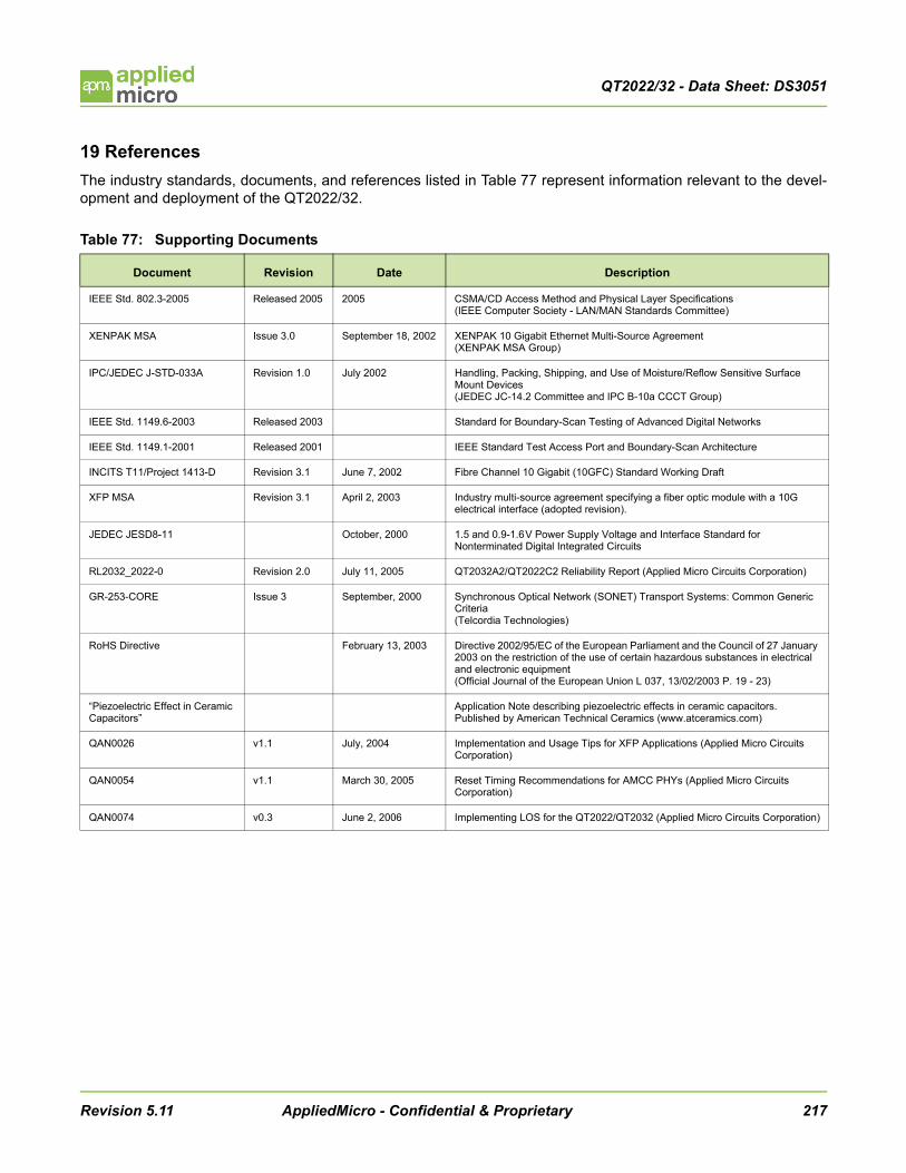
QT2022/32 - Data Sheet: DS3051
19 ReferencesThe industry standards, documents, and references listed in Table 77 represent information relevant to the devel-opment and deployment of the QT2022/32.
Table 77: Supporting Documents
Document Revision Date Description
IEEE Std. 802.3-2005 Released 2005 2005 CSMA/CD Access Method and Physical Layer Specifications (IEEE Computer Society - LAN/MAN Standards Committee)
XENPAK MSA Issue 3.0 September 18, 2002 XENPAK 10 Gigabit Ethernet Multi-Source Agreement(XENPAK MSA Group)
IPC/JEDEC J-STD-033A Revision 1.0 July 2002 Handling, Packing, Shipping, and Use of Moisture/Reflow Sensitive Surface Mount Devices(JEDEC JC-14.2 Committee and IPC B-10a CCCT Group)
IEEE Std. 1149.6-2003 Released 2003 Standard for Boundary-Scan Testing of Advanced Digital Networks
IEEE Std. 1149.1-2001 Released 2001 IEEE Standard Test Access Port and Boundary-Scan Architecture
INCITS T11/Project 1413-D Revision 3.1 June 7, 2002 Fibre Channel 10 Gigabit (10GFC) Standard Working Draft
XFP MSA Revision 3.1 April 2, 2003 Industry multi-source agreement specifying a fiber optic module with a 10G electrical interface (adopted revision).
JEDEC JESD8-11 October, 2000 1.5 and 0.9-1.6 V Power Supply Voltage and Interface Standard for Nonterminated Digital Integrated Circuits
RL2032_2022-0 Revision 2.0 July 11, 2005 QT2032A2/QT2022C2 Reliability Report (Applied Micro Circuits Corporation)
GR-253-CORE Issue 3 September, 2000 Synchronous Optical Network (SONET) Transport Systems: Common Generic Criteria (Telcordia Technologies)
RoHS Directive February 13, 2003 Directive 2002/95/EC of the European Parliament and the Council of 27 January 2003 on the restriction of the use of certain hazardous substances in electrical and electronic equipment(Official Journal of the European Union L 037, 13/02/2003 P. 19 - 23)
“Piezoelectric Effect in Ceramic Capacitors”
Application Note describing piezoelectric effects in ceramic capacitors. Published by American Technical Ceramics (www.atceramics.com)
QAN0026 v1.1 July, 2004 Implementation and Usage Tips for XFP Applications (Applied Micro Circuits Corporation)
QAN0054 v1.1 March 30, 2005 Reset Timing Recommendations for AMCC PHYs (Applied Micro Circuits Corporation)
QAN0074 v0.3 June 2, 2006 Implementing LOS for the QT2022/QT2032 (Applied Micro Circuits Corporation)
Revision 5.11 AppliedMicro - Confidential & Proprietary 217

QT2022/32 - Data Sheet: DS3051
Table 78: Revision History
Rev Date Description
5.11 April 7, 2010 Updated the “Revision History” notes for Revision 5.00 with additional details about the solder ball diam-eter (see underlined text).
5.10 March 11, 2010 Updated “WIS Synchronization (Octet and Frame Delineation)” on page 41 with more information on framing pattern.Added Section “SEF Defect Generation” on page 41, Section “LOF Defect Generation” on page 42 and “LOS Defect Generation” on page 42.Corrected typo on Section 8.4.1 on page 62 to reference register field 1.9002h.7 instead of 1.9002h.3. Updated marking drawing in Figure 55 on page 207 to include the AppliedMicro lot code (add Row #4)Indicated tolerances for parameters D and E of Package Outline Drawing in Figure 52 on page 203.Corrected turnaround (TA) timing in MDIO Read and Read Increment transactions in figure 23 on page 76.
5.00 December 16, 2009 Page 201, Package Outline Drawing updated. The nominal solder ball diameter (b) was changed from 0.46mm to 0.45mm, in accordance with JEDEC Standard Procedures and Practices. See JEDEC Publi-cation No. 95, SPP-003 Issue C, Item Number 11.2-740(S) for details.
2.03 November 4, 2009 Page 201, reference to ball diameter removed.Page 216, ordering information changed from QT2022PRKCB-1 to QT2022PRKCB
2.02 September 4, 2009 Page 206, added Marking DrawingPage 217, updated Ordering Information
2.01 March 4, 2008 Pg 13, Corrected description of EREFCLKC input. Added requirement for external AC coupling.
2.00 December 20, 2006 Increased maximum power consumption specification for WAN mode in Table 55 on page 187.Changed DJ specification for 10Gbps serial transmitter in Table 71 on page 198.Changed maximum current draw for XV1P2 and TV1P2 power supplies in Table 55 on page 187.Decreased maximum current draw for RV1P2 power supply in Table 55 on page 187.Added specification of maximum current draw for COREVCC power supply in Table 55 on page 187.Inserted additional Iol specification for MDIO in Table 60 on page 189 to show IEEE compliance.Changed pullup specification for 3.3V operation for MDIO in Table 60 on page 189.Corrected definition of 2.C500h bit 8 to be Reserved (RO); corrected definition of 2.C500h bit 9 to be “Far-end AIS-P/LOP-P” (RO)Corrected definition of 1.C003h bits 15:14 to remove 600kHz operation which is not supported by I2C.Corrected definition of “PHY_XS Code Error” to properly refer to the XAUI code violation fields in 4.C006h.3:0 in Table 25 on page 65.Updated bit field definition of 1.8.10 (PMA Receive Local Fault) and 1.8.11 (PMA Transmit Local Fault) to be consistent with Table 19 on page 58. Also updated text description of Section 8.2.4 on page 55 for consistency.Updated the definition of 2.C502h bits 7 and 6 to more accurately describe the behavior in Table 29 on page 68 and in the register map (2.C502h and 2.C501h updated).Corrected definition of “Receive Optical Power Fault” on page 126 to “RO”. Now consistent with definition in Table 24 on page 64.Corrected definition of MDIO register 2.C002h.9 to “WIS TX SS Bit Insert Enable” on page 151.Added text describing features and usage of WIS Tx OH Byte Insert feature in Section 7.3.9 on page 49.Updated definition of WIS register field 2.C000h.5 to match behavior as flag that detects NDF.
Note: In this document, deleted text is shown with a strikethrough. Inserted text is underlined.
1.02 October 13, 2006 Minor updates
1.01 September 19, 2006 Converted to AMCC format.
218 AppliedMicro - Confidential & Proprietary Revision 5.11

QT2022/32 - Data Sheet: DS3051
20 Ordering InformationTo order QT2032 and QT2022 products, quote the order number listed in Table 76.
Table 79: Ordering Information
Product description Product name Version Order number
QT2032 QT2032 A2, SnPb solder balls QT2032PBKCB
A2, SnAgCu solder balls QT2032PRKCB
QT2022 QT2022 C2, SnPb solder balls n/a
C2,SnAgCu solder balls QT2022PRKCB
QT2032A2/QT2022C2 Evaluation board 1
1. The evaluation board comes with a mounted QT2032. The QT2022 product can be evaluated by operating the QT2032 in LAN mode.
QT2032-EKG-1A2
QT2032A2 2-port XFP Reference Design Kit QT2032-RD7-1A2
Revision 5.11 AppliedMicro - Confidential & Proprietary 219

QT2022/32 - Data Sheet: DS3051
AppliedMicroTechnical Support: [email protected]
http://www.appliedmicro.com
AppliedMicro reserves the right to make changes to its products, its datasheets, or related documentation, without notice and war-rants its products solely pursuant to its terms and conditions of sale, only to substantially comply with the latest available datasheet. Please consult AppliedMicro’s Term and Conditions of Sale for its warranties and other terms, conditions and limitations. AppliedMi-cro may discontinue any semiconductor product or service without notice, and advises its customers to obtain the latest version of relevant information to verify, before placing orders, that the information is current. AppliedMicro does not assume any liability arising out of the application or use of any product or circuit described herein, neither does it convey any license under its patent rights nor the rights of others. AppliedMicro reserves the right to ship devices of higher grade in place of those of lower grade. APPLIEDMICRO SEMICONDUCTOR PRODUCTS ARE NOT DESIGNED, INTENDED, AUTHORIZED, OR WARRANTED TO BE SUITABLE FOR USE IN LIFE-SUPPORT APPLICATIONS, DEVICES OR SYSTEMS OR OTHER CRITICAL APPLICATIONS. AppliedMicro is a registered Trademark of Applied Micro Circuits Corporation. Copyright © 2010 Applied Micro Circuits Corporation.
I2C BUS® is a registered trademark of Philips Electronics N.V. Corporation Netherlands
220 AppliedMicro - Confidential & Proprietary Revision 5.11